

Sony SA-WMS356, SA-WMS556 Service Manual
SERVICE MANUAL
Sony Corporation
Home Audio Company
Published by Sony Engineering Corporation
AEP Model
UK Model
SUBWOOFER
9-877-843-01
2004E0478-1
© 2004.05
Ver 1.0 2004.05
SPECIFICATIONS
SA-WMS356/WMS556
• SA-WMS356/WMS556 are the subwoofer
section in SA-VE356T/VE556H.
Speaker system Active subwoofer,
magnetically shielded
Speaker unit Woofer: 15 cm × 2, cone type
Enclosure type Acoustically loaded
Bass Reflex
Reproduction frequency range
28 Hz - 200 Hz
Amplifier section
Continuous RMS power output
SA-WMS356:
120 W (6 ohms, 100 Hz,
10 % THD)
SA-WMS556:
150 W (6 ohms, 100 Hz,
10 % THD)
Inputs
INPUT (input pin jack)
General
Power requirements
230 - 240 V AC, 50/60 Hz
Power consumptions
120 W
1 W (standby mode)
Dimensions (w/h/d)
Approx. 180 × 405 × 501 mm,
including front grille
Mass Approx. 12 kg
Design and specifications are subject to change
without notice.

2
SA-WMS356/WMS556
SAFETY-RELATED COMPONENT WARNING!!
COMPONENTS IDENTIFIED BY MARK 0 OR DOTTED LINE
WITH MARK 0 ON THE SCHEMATIC DIAGRAMS AND IN
THE PARTS LIST ARE CRITICAL TO SAFE OPERATION.
REPLACE THESE COMPONENTS WITH SONY PAR TS WHOSE
PART NUMBERS APPEAR AS SHO WN IN THIS MANU AL OR
IN SUPPLEMENTS PUBLISHED BY SONY.
UNLEADED SOLDER
Boards requiring use of unleaded solder are printed with the leadfree mark (LF) indicating the solder contains no lead.
(Caution: Some printed circuit boards may not come printed with
the lead free mark due to their particular size)
: LEAD FREE MARK
Unleaded solder has the following characteristics.
• Unleaded solder melts at a temperature about 40 °C higher
than ordinary solder.
Ordinary soldering irons can be used but the iron tip has to be
applied to the solder joint for a slightly longer time.
Soldering irons using a temperature regulator should be set to
about 350 °C.
Caution: The printed pattern (copper foil) may peel away if
the heated tip is applied for too long, so be careful!
• Strong viscosity
Unleaded solder is more viscou-s (sticky, less prone to flow)
than ordinary solder so use caution not to let solder bridges
occur such as on IC pins, etc.
• Usable with ordinary solder
It is best to use only unleaded solder but unleaded solder may
also be added to ordinary solder.
TABLE OF CONTENTS
1. DIAGRAMS
1-1. Printed Wiring Board – MAIN Section – ........................ 5
1-2. Schematic Diagram – MAIN Section –........................... 6
1-3. Printed Wiring Board – CONTROL Section –................ 7
1-4. Schematic Diagram – CONTROL Section –................... 8
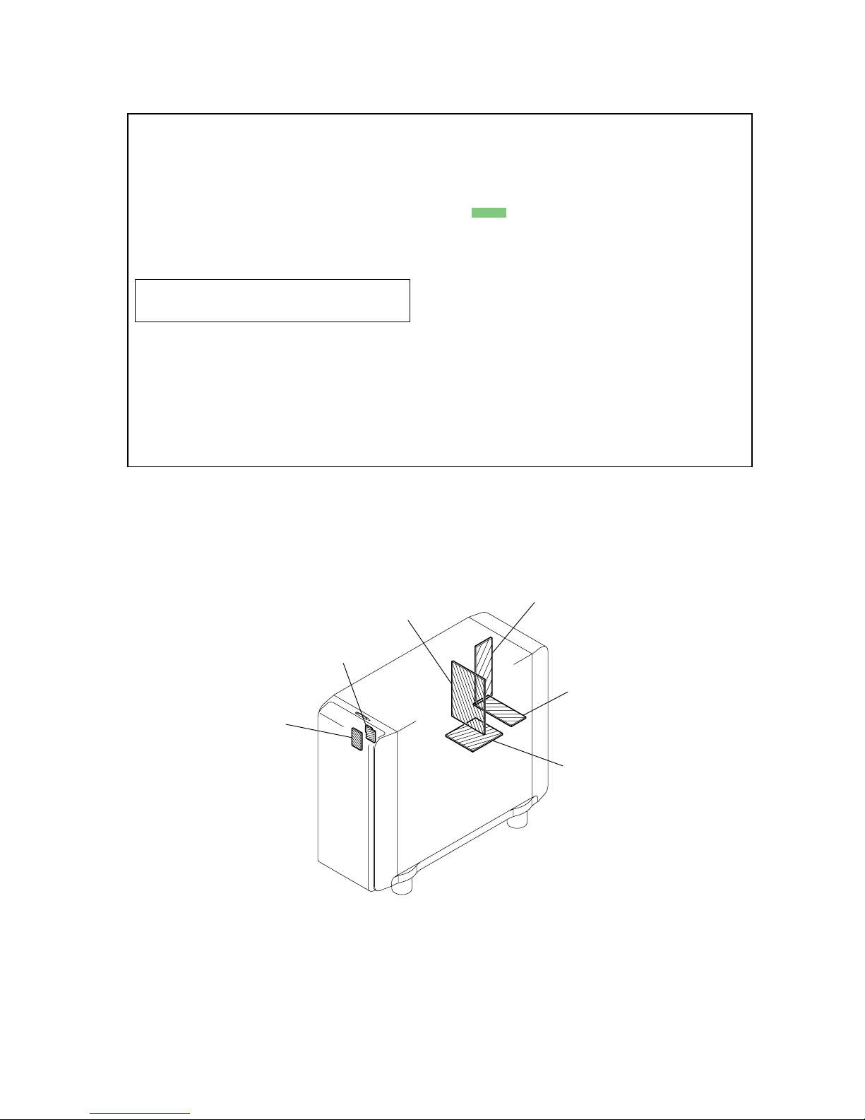
2. EXPLODED VIEWS
2-1. Front Panel Section ......................................................... 9
2-2. Rear Cover Section .......................................................... 10
2-3. Bottom Panel Section ...................................................... 11
3. ELECTRICAL PARTS LIST .................................. 12
3
SA-WMS356/WMS556
SECTION 1
DIAGRAMS
For Schematic Diagrams.
Note:
• All capacitors are in µF unless otherwise noted. (p: pF)
50 WV or less are not indicated except f or electrolytics and
tantalums.
• All resistors are in Ω and 1/
4
W or less unless otherwise
specified.
• f : internal component.
• C : panel designation.
• A : B+ Line.
• B : B– Line.
•Voltages and wavef orms are dc with respect to ground under no-signal (detuned) conditions.
no mark: Power on
•Voltages are taken with a VOM (Input impedance 10 MΩ).
Voltage v ariations ma y be noted due to normal production
tolerances.
• Signal path.
F : AUDIO
For Printed Wiring Boards.
Note:
• X : parts extracted from the component side.
• Y : parts extracted from the conductor side.
• : Pattern from the side which enables seeing.
THIS NOTE IS COMMON FOR PRINTED WIRING BOARDS AND SCHEMATIC DIAGRAMS.
(In addition to this, the necessary note is printed in each block.)
Note: The components identified by mark 0 or dotted
line with mark 0 are critical for safety.
Replace only with part number specified.
LED board
MAIN board
CONTROL board
POWER AMP board
POWER SUPPLY board
POWER SWITCH board
NOTE FOR PRINTED WIRING BOARDS AND SCHEMATIC DIAGRAMS
• Circuit Boards Location
4
SA-WMS356/WMS556
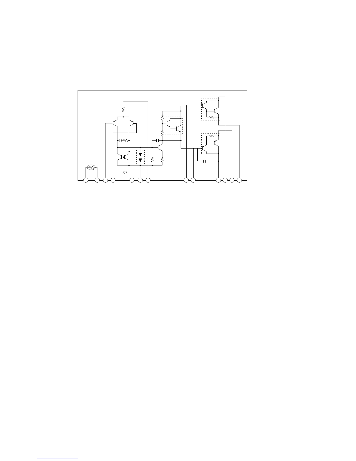
1 2 3 4 5 6 7 8 9 10 11 12 13
IC701 STK404-140S
• IC Block Diagram
– POWER AMP Board –
55
SA-WMS356/WMS556
1
A
B
C
D
E
F
G
H
I
234567891011 12 13 14
C713
Q702
R706
C701
R702
R703
R701
CN701
C707
R708
R714
C710
D701
D702
D703
Q701
R711
R709
R710
R707
C705
R705
R712
R713
R704
C712
JW703
JW704
JW
707
C702
C704
IC701
R715
R716
R717
C703
C708
C709
C706
JW
705
JW
708
JW
702
JW
701
CN702
C711
JW
709
C716
JW
711
C715
C714
D202
BC201
BC903
T102
CN1
F901
T202
C901
D901
RY901
BC901
BC902
F11
F12
JW
053
JW
052
JW
051
C902
CN904
C201
S201
BC202
BC801
D805
C801
C802
C803
C804
BC802
R303
R304
C301
C302
C305
C306
C307
C308
D301
D302
D303
D304
D305
D306
R101
R102
R103
R104
R105
R106
C101
C102
Q104
Q105
R531
R532
R534
R535
R536
R537
R538
R539
R540
R542
C531
D532
D533
R404
R405
R400
D400
D401
C401
C403
Q401
Q402
Q403
RY400
BC401
CN804
CN805
IC530
BC803
Q532
R533
D531
R401
R406
G1
G2
JW
801
JW802
JW807
JW
809
JW
810
JW
811
JW813
JW814
JW816
JW
817
JW
818
JW
819
JW820
JW821
JW822
JW823
JW
824
JW825
JW826
JW
828
JW
829
JW830
JW832
JW833
C303
C304
JW808
C532
Q404
Q533
Q534
Q535
JW
834
JW835
JW812
Q102
Q101
Q103
JW837
C402
JW827
R402
R403
Q301
Q302
Q531
C806
JW
805
JW804
C805
R800
JW301
JW302
R541
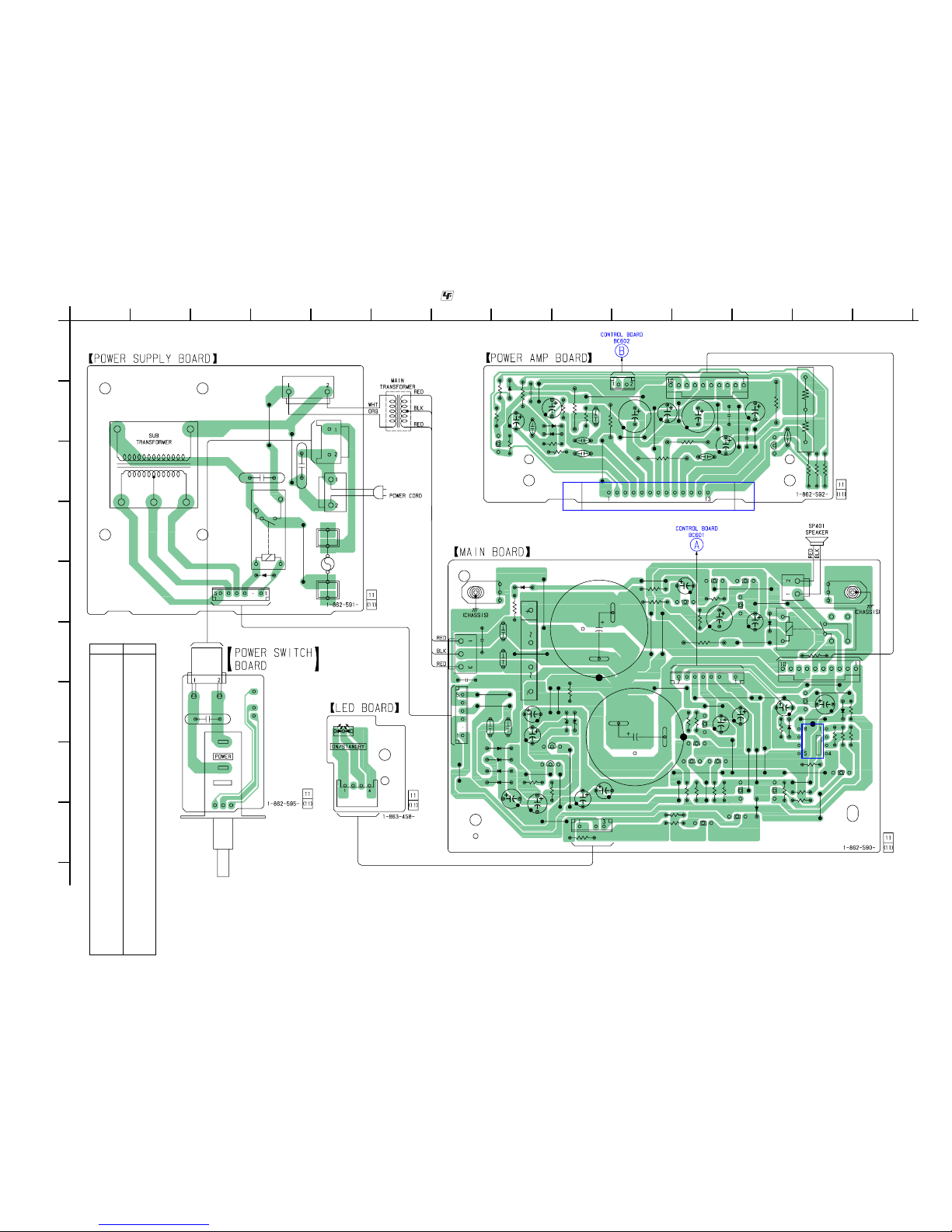
1-1. PRINTED WIRING BOARD — MAIN SECTION —
• See page 3 for Circuit Boards Location. :Uses unleaded solder.
• Semiconductor
Location
Ref. No.
Location
D202 I-3
D301 H-8
D302 H-8
D303 H-8
D304 I-8
D305 H-9
D306 H-9
D400 F-12
D401 E-8
D531 H-12
D532 G-13
D533 I-12
D701 B-9
D702 B-9
D703 B-8
D805 F-8
D901 E-4
IC530 H-13
IC701 C-10
Q101 H-11
Q102 H-11
Q103 H-11
Q104 I-12
Q105 H-11
Q301 H-9
Q302 H-9
Q401 F-11
Q402 E-11
Q403 F-12
Q404 E-12
Q531 G-13
Q532 I-12
Q533 H-13
Q534 I-12
Q535 I-11
Q701 C-8
Q702 C-12
(Page 7)
(Page 7)
 Loading...