

Page 1
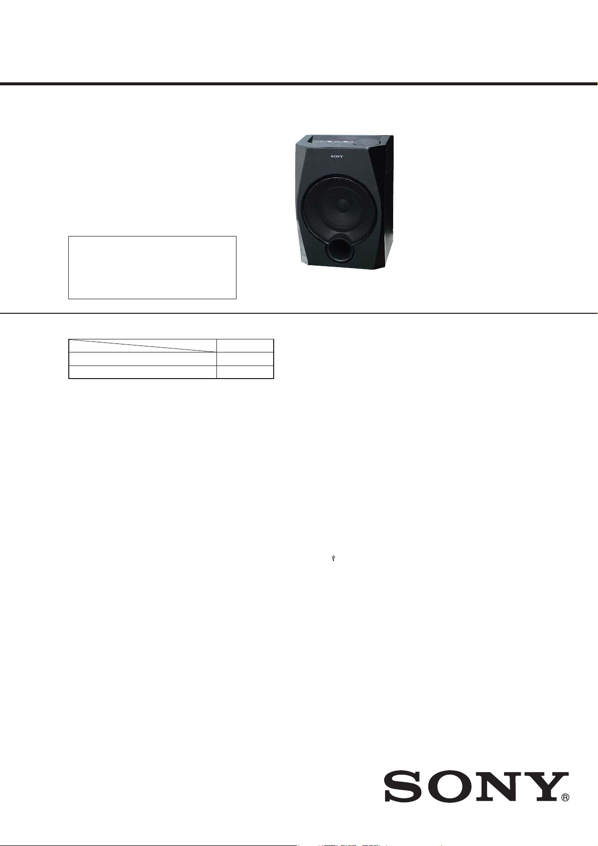
HT-GT1
T
SA-WGT1
SERVICE MANUAL
Ver. 1.2 2015.01
• All of the units included in the HT-GT1 (SA-WGT1/SS-GT1)
are required to confi rming operation of SA-WGT1. Check in
advance that you have all of the units.
Note:
Be sure to keep your PC used for service and
checking of this unit always updated with the
latest version of your anti-virus software.
In case a virus affected unit was found during
service, contact your Service Headquarters.
COMPONENT MODEL NAME
HT-GT1
Bar Speaker (Speaker System) SS-GT1
Subwoofer (Active Subwoofer) SA-WGT1
• Please refer to service manual separately issued for Bar
Speaker.
US Model
AEP Model
UK Model
E Model
Australian Model
Amplier section
U.S. model:
POWER OUTPUT AND TOTAL
HARMONIC DISTORTION (FTC output
power):
Front L/Front R:
With 3 ohms loads, both channels
driven, from 400 – 10,000 Hz;
rated 32 watts per channel
minimum RMS power, with no
more than 1.0% total harmonic
distortion from 250 milliwatts to
rated output.
Output power (reference):
Front L/Front R:
40 W + 40 W (per channel at 3
kHz)
ohms, 1
Subwoofer:
180 W (at 4 ohms, 100 Hz)
Brazilian model:
otal RMS output power:
200W
Front L/Front R:
RMS output power:
80W (40W per channel × 2, at
3ohms, 1kHz, 10% THD*)
Subwoofer:
RMS output power:
120W (at 4ohms, 100Hz, 10%
THD*)
Other models:
Power output (rated):
Front L/Front R:
32 W + 32 W (at 3 ohms, 1 kHz, 1%
THD*)
Power output (reference):
Front L/Front R:
40 W + 40 W (per channel at
3ohms, 1 kHz)
Subwoofer:
180 W (at 4 ohms, 100 Hz)
* Total Harmonic Distortion
Speaker section
Speaker system:
Subwoofer, Bass reflex
Speaker unit:
1
180 mm (7
Rated impedance:
Inputs
AUDIO IN/PARTY CHAIN IN L/R:
OPT IN:
Outputs
AUDIO OUT/PARTY CHAIN OUT L/R:
Tuner section
FM stereo, FM superheterodyne tuner
Antenna:
Tuning range:
/8 in), cone type
4 ohms
Voltage 0.8 V, impedance
47 kilohms
Supported audio signal:
2-channel Linear PCM
Voltage 2 V, impedance 1 kilohm
FM lead antenna
USA and Brazilian models:
87.5MHz - 108.0MHz (100kHz
step)
Other models:
87.5MHz - 108.0MHz (50kHz
step)
SPECIFICATIONS
BLUETOOTH section
Communication system:
BLUETOOTH Standard version 3.0
Output:
BLUETOOTH Standard Power
Class 2
Maximum communication range:
Line of sight approx. 10 m
1)
(33 feet)
Frequency band:
2.4 GHz band (2.4000 GHz –
2.4835 GHz)
Modulation method:
FHSS (Freq Hopping Spread
Spectrum)
Compatible BLUETOOTH profiles
A2DP (Advanced Audio
Distribution Profile)
AVRCP 1.3 (Audio Video Remote
Control Profile)
Supported codecs:
SBC (Sub Band Codec)
AAC (Advanced Audio Coding)
1)
The actual r ange will vary depending
on factors such as obstacles between
devices, magnetic fields around a
microwave oven, static electricity,
reception sensitivity, antenna’s
performance, operating system,
software application, etc.
2)
BLUETOOTH standard profiles
indicate the purpose of BLUETOOTH
communication between devices.
2)
:
USB section
Supported format:
MP3 (MPEG 1 Audio Layer-3):
32 kbps – 320 kbps, VBR
WMA:
48 kbps – 192 kbps
AAC:
48 kbps – 320 kbps
WAV:
16 bit PCM
Sampling frequencies:
MP3 (MPEG 1 Audio Layer-3):
32 kHz/44.1 kHz/48 kHz
WMA:
32 kHz/44.1 kHz/48 kHz
AAC:
32 kHz/44.1 kHz/48 kHz
WAV:
8 kHz – 48 kHz
Supported USB device:
Mass Storage Class
Maximum current:
1 A
(USB) port:
Type A
General
Power requirements:
USA and Mexican models:
AC 120 V, 60 Hz
Latin American model (except for
Bolivian, Chilean, Argentine, and
Mexican models):
AC 110 V – 240 V, 50/60 Hz
Saudi Arabian,African and Irarian
models:
AC 120 V – 240 V, 50/60 Hz
Other models:
AC 220 V – 240 V, 50/60 Hz
Power consumption:
70 W
Power consumption (at the Power
Saving mode):
European model:
0.5 W (When BLUETOOTH standby
mode is set to off)
6 W (When BLUETOOTH standby
mode is set to on)
Other models:
0.5 W
Dimensions (W/H/D) (Approx.):
Active subwoofer:
290 mm × 420 mm × 275 mm
3
/8 in × 16 1/2 in × 10 7/8 in )
(11
Speaker system:
800 mm × 110 mm × 102 mm
1
/2 in × 4 3/8 in × 4 in )
(31
Mass (Approx.):
Active subwoofer:
1
7.1 kg (15 lb 10
/2 oz)
Speaker system:
3
/4 oz)
2.8 kg (6 lb 2
Quantity:
Active subwoofer:
1 piece
Speaker system:
1 piece
Supplied accessories
Optical digital cable (1)
Remote control (1)
R03 (Size AAA) batteries (2)
FM lead antenna (1)
Design and specifications are subject
to change without notice.
HT-GT1
SOUND BAR
SA-WGT1
ACTIVE SUBWOOFER
9-896-032-03
2015A33-1
2015.01
©
Sony Corporation
Published by Sony Techno Create Corporation
Page 2

HT-GT1
Ver. 1.1
License and Trademark Notice
MPEG Layer-3 audio coding
technology and patents licensed
from Fraunhofer IIS and Thomson.
Windows Media is either a
registered trademark or trademark
of Microsoft Corporation in
the United States and/or other
countries.
This product is protected by
certain intellectual property rights
of Microsoft Corporation. Use or
distribution of such technology
outside of this product is prohibited
without a license from Microsoft or
an authorized Microsoft subsidiary.
The BLUETOOTH® word mark and
logos are registered trademarks
owned by Bluetooth SIG, Inc. and
any use of such marks by Sony
Corporation is under license. Other
trademarks and trade names are
those of their respective owners.
The N Mark is a trademark or
registered trademark of NFC Forum,
Inc. in the United States and in other
countries.
Android™ is a trademark of Google
Inc.
Google Play™ is a trademark of
Google Inc.
iPhone and iPod touch are
trademarks of Apple Inc., registered
in the U.S. and other countries. App
Store is a service mark of Apple Inc.
“Made for iPod” and “Made for
iPhone” mean that an electronic
accessory has been designed
to connect specifically to iPod
or iPhone, respectively, and has
been certified by the developer
to meet Apple performance
standards. Apple is not responsible
for the operation of this device
or its compliance with safety and
regulatory standards. Please note
that the use of this accessory with
iPod or iPhone may affect wireless
performance.
All other trademarks and registered
trademarks are of their respective
holders. In this manual, ™ and ®
marks are not specified.
NOTES ON CHIP COMPONENT REPLACEMENT
• Never reuse a disconnected chip component.
• Notice that the minus side of a tantalum capacitor may be damaged by heat.
SAFETY CHECK-OUT
After correcting the original service problem, perform the following safety check before releasing the set to the customer:
Check the antenna terminals, metal trim, “metallized” knobs,
screws, and all other exposed metal parts for AC leakage.
Check leakage as described below.
LEAKAGE TEST
The AC leakage from any exposed metal part to earth ground and
from all exposed metal parts to any exposed metal part having a
return to chassis, must not exceed 0.5 mA (500 microamperes.).
Leakage current can be measured by any one of three methods.
1. A commercial leakage tester, such as the Simpson 229 or RCA
WT-540A. Follow the manufacturers’ instructions to use these
instruments.
2. A battery-operated AC milliammeter. The Data Precision 245
digital multimeter is suitable for this job.
3. Measuring the voltage drop across a resistor by means of a
VOM or battery-operated AC voltmeter . The “limit” indication
is 0.75 V, so analog meters must have an accurate low-voltage
scale. The Simpson 250 and Sanwa SH-63Trd are examples
of a passive VOM that is suitable. Nearly all battery operated
digital multimeters that have a 2 V AC range are suitable. (See
Fig. A)
To Exposed Metal
Parts on Set
AC
1.5 kΩ0.15 μF
Earth Ground
voltmeter
(0.75 V)
Fig. A. Using an AC voltmeter to check AC leakage.
SAFETY-RELATED COMPONENT WARNING!
COMPONENTS IDENTIFIED BY MARK 0 OR DOTTED LINE
WITH MARK 0 ON THE SCHEMATIC DIAGRAMS AND IN
THE PARTS LIST ARE CRITICAL TO SAFE OPERATION.
REPLACE THESE COMPONENTS WITH SONY PARTS
WHOSE PART NUMBERS APPEAR AS SHOWN IN THIS
MANUAL OR IN SUPPLEMENTS PUBLISHED BY SONY.
2
Page 3

TABLE OF CONTENTS
HT-GT1
1. SERVICING NOTES ............................................. 4
2. DISASSEMBLY
2-1. Disassembly Flow ........................................................... 6
2-2. Side L, R Panel ............................................................... 7
2-3. Top Panel Block .............................................................. 8
2-4. Front Panel Block ........................................................... 9
2-5. NFC Module (NFC1) ...................................................... 10
2-6. Bluetooth Module (BT1) ................................................ 11
2-7. PANEL Board Block ....................................................... 12
2-8. Button Assy ..................................................................... 13
2-9. Knob Assy ....................................................................... 14
2-10. Top Panel Assy ................................................................ 15
2-11. Rear Panel Block ............................................................ 16
2-12. DC Fan (M1) ................................................................... 17
2-13. TUNER Board ................................................................ 17
2-14. MAIN Board-1 ................................................................ 18
2-15. MAIN Board-2 ................................................................ 19
2-16. Sub Chassis ..................................................................... 20
2-17. Power Cord (AC1) .......................................................... 21
2-18. SMPS Board ................................................................... 22
2-19. Loudspeaker (18 cm) (SP1) ............................................ 23
2-20. Service Position .............................................................. 24
3. TEST MODE ............................................................ 25
4. ELECTRICAL CHECK ......................................... 27
5. TROUBLESHOOTING .......................................... 28
6. DIAGRAMS
6-1. Block Diagram - MAIN Section - ................................... 29
6-2. Block Diagram - AMP Section - ..................................... 30
6-3. Block Diagram
- PANEL/POWER SUPPLY Section - ............................ 31
6-4. Schematic Diagram - MAIN Section (1/5) - ................... 33
6-5. Schematic Diagram - MAIN Section (2/5) - ................... 34
6-6. Schematic Diagram - MAIN Section (3/5) - ................... 35
6-7. Schematic Diagram - MAIN Section (4/5) - ................... 36
6-8. Schematic Diagram - MAIN Section (5/5) - ................... 37
6-9. Printed Wiring Boards - MAIN Section (1/2) - .............. 38
6-10. Printed Wiring Board - MAIN Section (2/2) - ................ 39
6-11. Printed Wiring Boards - KEY Section - .......................... 40
6-12. Schematic Diagram - KEY Section - .............................. 41
6-13. Printed Wiring Board - PANEL Board - ......................... 42
6-14. Schematic Diagram - PANEL Board - ............................ 43
6-15. Printed Wiring Board - SMPS Board - ........................... 44
6-16. Schematic Diagram - SMPS Board - .............................. 45
7. EXPLODED VIEWS
7-1. Side Panel Section .......................................................... 53
7-2. Top Panel Section ........................................................... 54
7-3. Front Panel Section ......................................................... 55
7-4. MAIN Board Section ...................................................... 56
7-5. SMPS Board Section ...................................................... 57
7-6. Speaker Cabinet Section ................................................. 58
8. ELECTRICAL PARTS LIST .............................. 59
Accessories are given in the last of the electrical parts list.
3
Page 4
HT-GT1
Ver. 1.2
SECTION 1
SERVICING NOTES
The SERVICING NOTES contains important information for servicing. Be sure to read this section before repairing the unit.
UNLEADED SOLDER
Boards requiring use of unleaded solder are printed with the leadfree mark (LF) indicating the solder contains no lead.
(Caution: Some printed circuit boards may not come printed with
the lead free mark due to their particular size)
: LEAD FREE MARK
Unleaded solder has the following characteristics.
• Unleaded solder melts at a temperature about 40 °C higher
than ordinary solder.
Ordinary soldering irons can be used but the iron tip has to be
applied to the solder joint for a slightly longer time.
Soldering irons using a temperature regulator should be set to
about 350 °C.
Caution: The printed pattern (copper foil) may peel away if
the heated tip is applied for too long, so be careful!
• Strong viscosity
Unleaded solder is more viscous (sticky, less prone to fl ow)
than ordinary solder so use caution not to let solder bridges
occur such as on IC pins, etc.
• Usable with ordinary solder
It is best to use only unleaded solder but unleaded solder may
also be added to ordinary solder.
CAPACITOR ELECTRICAL DISCHARGE PROCESSING
When checking the board, for the electric shock prevention, connect the resistors to both ends of resistor (R156) to discharge the
capacitor (C129).
– SMPS Board (Component Side) –
800 :/2 W
R156
C129
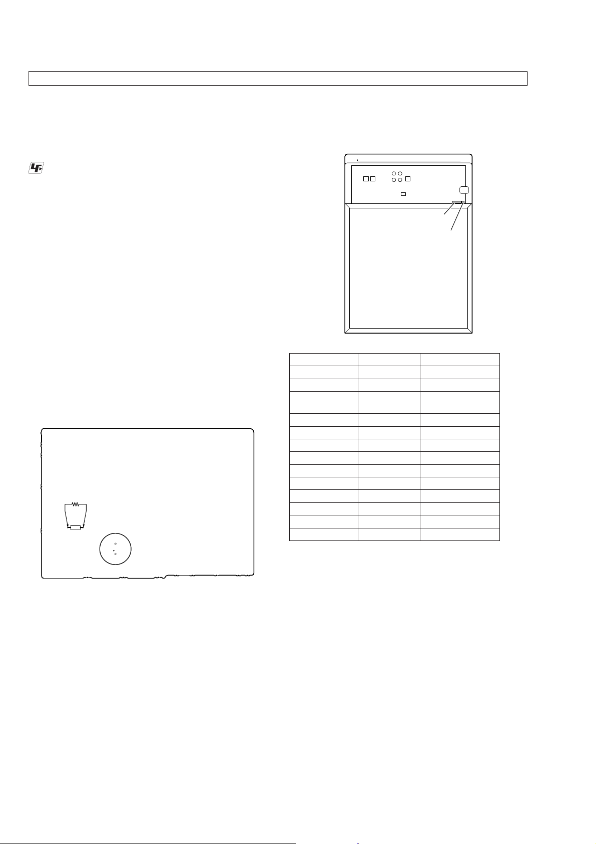
MODEL IDENTIFICATION
Distinguish by Part No. and destination code on the back side of
a main unit.
– Back panel view –
Part No.
Destination code
Destination Part No. Destination code
Latin American
US
Indian, African,
Iranian
AEP, UK
Brazilian
Chilean, Peruvian
Mexican
Argentina
Saudi Arabia
Russian
Singapore
Australian
Thai
4-540-495-0[]
4-540-495-1[]
4-540-495-2[]
4-540-495-3[]
4-540-495-4[]
4-540-495-5[]
4-540-495-6[]
4-540-495-7[]
4-540-495-8[]
4-540-495-9[]
4-543-516-0[]
4-543-516-1[]
4-543-516-2[]
E32
U2
E12, E3
CEL, CEK
BR1
E51
MX2
AR2
EA3
RU3
SP1
AU1
TH1
DESTINATION ABBREVIATIONS
The following abbreviations for model destinations are used in this
service manual.
• Abbreviations
AR : Argentina model
AUS : Australian model
BR : Brazilian model
E3 : African and Iranian models
E12 : Indian model
E32 : Latin American model
E51 : Chilean and Peruvian models
EA : Saudi Arabia model
MX : Mexican model
RU : Russian model
SP : Singapore model
TH : Thai model
4
Page 5
ADVANCE PREPARATION WHEN CONFIRMING OPERATION
All of the units included in the HT-GT1 (SA-WGT1/SS-GT1) are
required to confi rming operation of SA-WGT1. Check in advance
that you have all of the units.
NOTE OF PERFORMING THE OPERATION CHECK IN
THE STATE THAT HEAT SINK WAS REMOVED
When performing the operation check in the state that this unit was
disassembled, it is possible to perform the operation check in the
state that heat sink was removed. But don’t perform the operation
check in the long time, and perform the operation check in the
volume state as low as possible.
NOTE OF REPLACING THE TUNER BOARD
When the TUNER board is defective, replace the complete mounted board.
NOTE OF REPLACING THE IC1002 AND IC4001 ON
THE MAIN BOARD
IC1002 and IC4001 on the MAIN board cannot replace with single. When these parts are damaged, replace the complete mounted
board.
HT-GT1
NOTE OF REPLACING THE IC002 ON THE MAIN
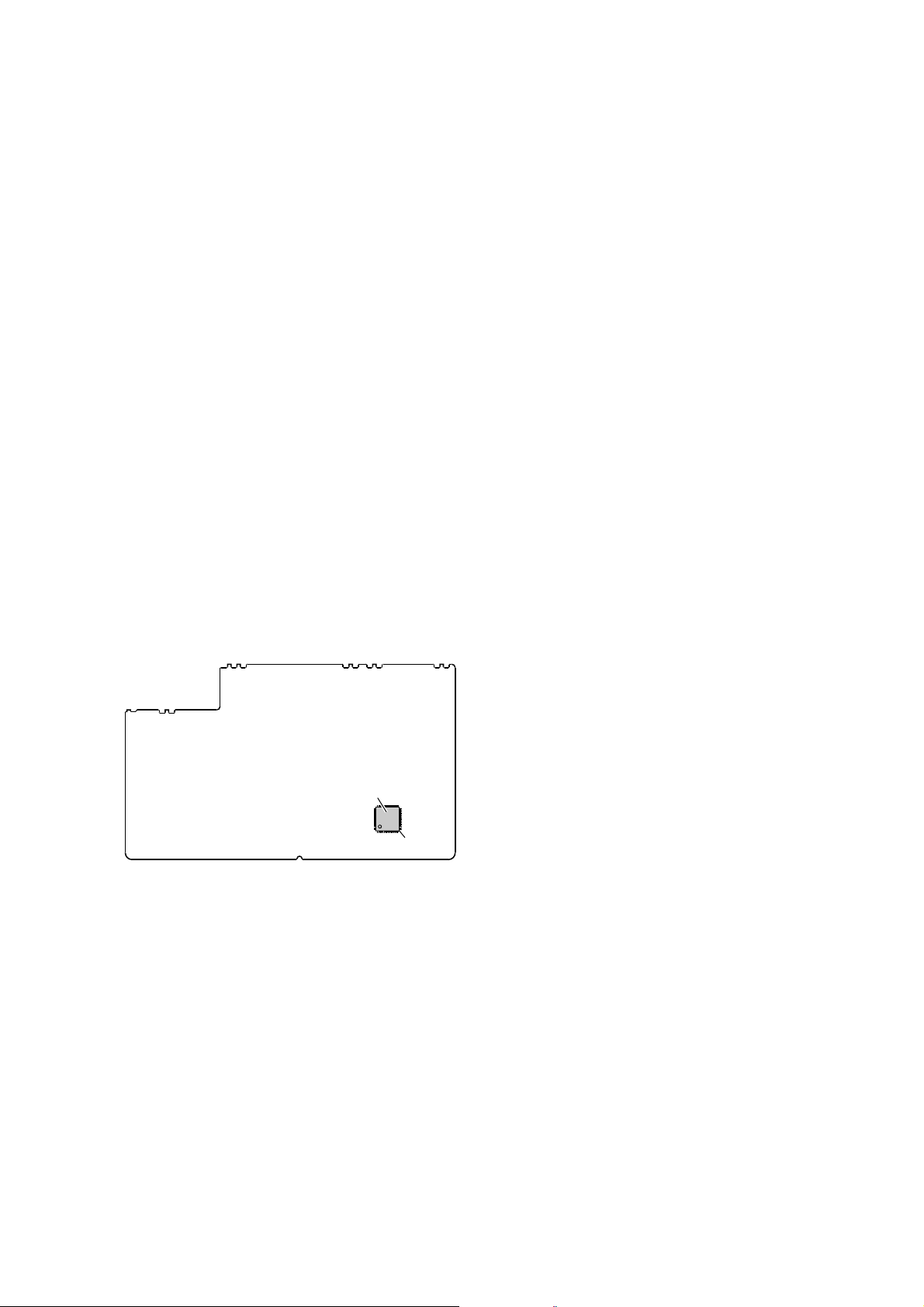
BOARD AND THE COMPLETE MAIN BOARD
When IC002 on the MAIN board and the complete MAIN board
are replaced, it is necessary to spread the compound between the
MAIN board and the heat sink.
Spread the compound (THERMAL COMPOUND (G747)) referring to the fi gure below.
– MAIN Board (Component Side) –
thermal compound (G747)
IC002
5
Page 6
HT-GT1
DISASSEMBLY
• This set can be disassembled in the order shown below.
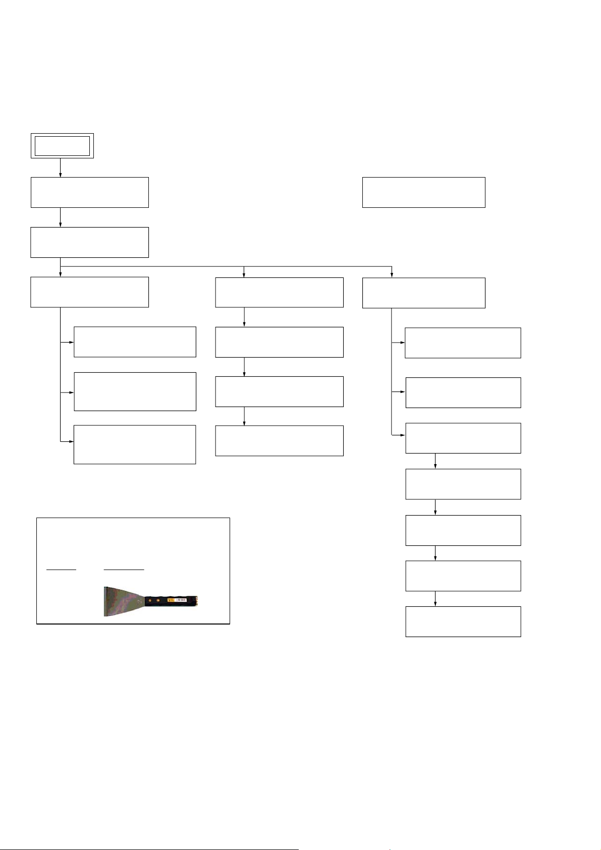
2-1. DISASSEMBLY FLOW
SET
SECTION 2
2-2. SIDE L, R PANEL
(Page 7)
2-3. TOP PANEL BLOCK
(Page 8)
2-4. FRONT PANEL BLOCK
(Page 9)
2-5. NFC MODULE (NFC1)
(Page 10)
2-6. BLUETOOTH MODULE
(BT1)
(Page 11)
2-19. LOUDSPEAKER (18 cm)
(SP1)
(Page 23)
2-7. PANEL BOARD BLOCK
(Page 12)
2-8. BUTTON ASSY
(Page 13)
2-9. KNOB ASSY
(Page 14)
2-10. TOP PANEL ASSY
(Page 15)
2-20. SERVICE POSITION
(Page 24)
2-11. REAR PANEL BLOCK
(Page 16)
2-12. DC FAN (M1)
(Page 17)
2-13. TUNER BOARD
(Page 17)
2-14. MAIN BOARD-1
(Page 18)
2-15. MAIN BOARD-2
(Page 19)
JIG
When disassembling the unit, use the following
jig for speaker removal.
Part No. Description
J-2501-238-A JIG FOR SPEAKER REMOVAL
2-16. SUB CHASSIS
(Page 20)
2-17. POWER CORD (AC1)
(Page 21)
2-18. SMPS BOARD
(Page 22)
6
Page 7
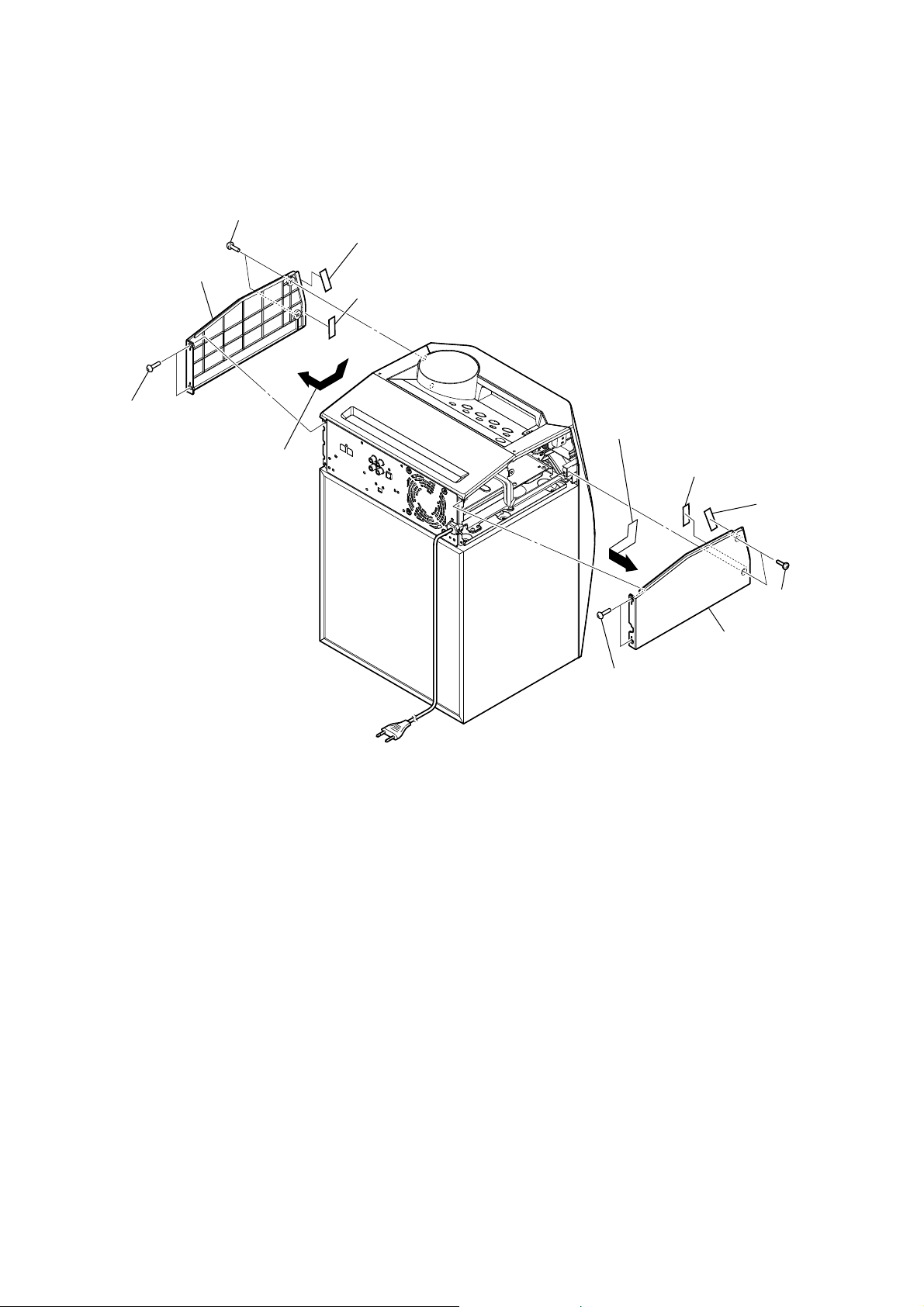
Note: Follow the disassembly procedure in the numerical order given.
2-2. SIDE L, R PANEL
1 two tapping
screws (HEX)
6 side R panel
2 two screws
(BVTP3 u 10)
3 Remove the side R panel block
in the direction of the arrow.
4 saranet cushion
(10T25)
4 saranet cushion
(10T25)
HT-GT1
3 Remove the side L panel block
in the direction of the arrow.
5 saranet cushion
(7T25)
4 saranet cushion
(10T25)
– Rear view –
1 two tapping
screws (HEX)
6 side L panel
2 two screws
(BVTP3 u 10)
7
Page 8
HT-GT1
2-3. TOP PANEL BLOCK
8 top panel block
5 Lift up the top panel block
in the direction of the arrow.
4 seven claws
2 screw
(BV3)
:LUHVHWWLQJ
MAIN board
rear
side
CN3004
6 connector
(CN1001)
7 flexible flat cable (13P)
(CN3004)
3 two screws
(BVTP3 u 10)
– Rear view –
flexible flat cable (13P)
Pass the flexible flat cable (13P)
Note 1:
underneath the clamp.
1 Remove the wire
from the clamp.
1 Remove the wire
from the clamp.
:LUHVHWWLQJ
SMPS board
rear
side
When installing the flexible flat cable, ensure that
Note 2:
the colored line is parallel to the connector after insertion.
OK
Insert straight into the interior.
flexible flat
cable
colored line
connector
clamp
Insert at a slant.
flexible flat
cable
colored line
connector
clamp
clamp
NG
8
Page 9
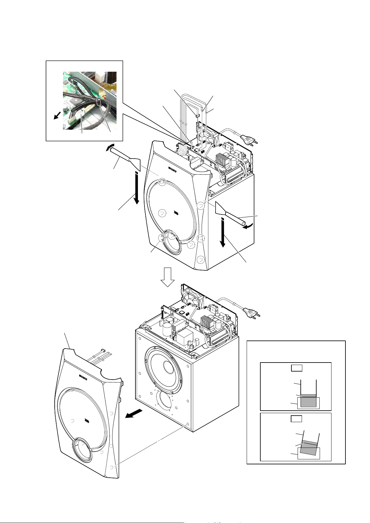
2-4. FRONT PANEL BLOCK
:LUHVHWWLQJ
rear
side
MAIN board
5 Insert the jig into the space and slowly
remove the front panel block.
Note 1: When using a jig, please work
carefully so as not to damage
the front panel block and
speaker cabinet.
clamp
4 connector
(CN3005)
1 Remove the wire
from the clamp.
HT-GT1
3 flexible flat cable (14P)
(CN3003)
2 flexible flat cable (8P)
(CN3002)
6 While moving the jig in the direction
of the arrow, remove all bosses and
the front panel block.
total eight bosses
7 front panel block
5 Insert the jig into the space and slowly
remove the front panel block.
Note 1: When using a jig, please work
carefully so as not to damage
the front panel block and
speaker cabinet.
6 While moving the jig in the direction
of the arrow, remove all bosses and
the front panel block.
When installing the flexible flat cable,
Note 2:
ensure that the colored line is parallel
to the connector after insertion.
OK
Insert straight into the interior.
flexible flat
cable
colored line
connector
Insert at a slant.
flexible flat
cable
colored line
connector
NG
9
Page 10
HT-GT1
2-5. NFC MODULE (NFC1)
:LUHVHWWLQJ
top side
filament tape
(sub material)
flexible flat cable (8P)
NFC holder
NFC holder block
2 filament tape
(sub material)
5 filament tape
(sub material)
3 screw
(BVTP2.6)
+RZWRLQVWDOOWKHIOH[LEOHIODWFDEOH3
flexible flat cable (8P)
The lower side is
the terminal side.
6 flexible flat cable (8P)
(FFC3)
8 NFC module
(NFC1)
7 Peel the NFC module (NFC1)
off of the PSA tape (5T15).
Remove the
4
in the direction of the arrow.
NFC module block
–)URQWSDQHOEORFNUHDUERWWRPYLHZ–
When installing the flexible flat cable, ensure that
Note:
the colored line is parallel to the connector after insertion.
OK
Insert straight into the interior.
flexible flat
cable
colored line
connector
flexible flat
cable
colored line
connector
NG
Insert at a slant.
1 Remove the wire
from the clamp.
:LUHVHWWLQJ
top side
flexible flat cable (8P)
clamp
1 Remove the wire
from the clamp.
clamp
10
Page 11
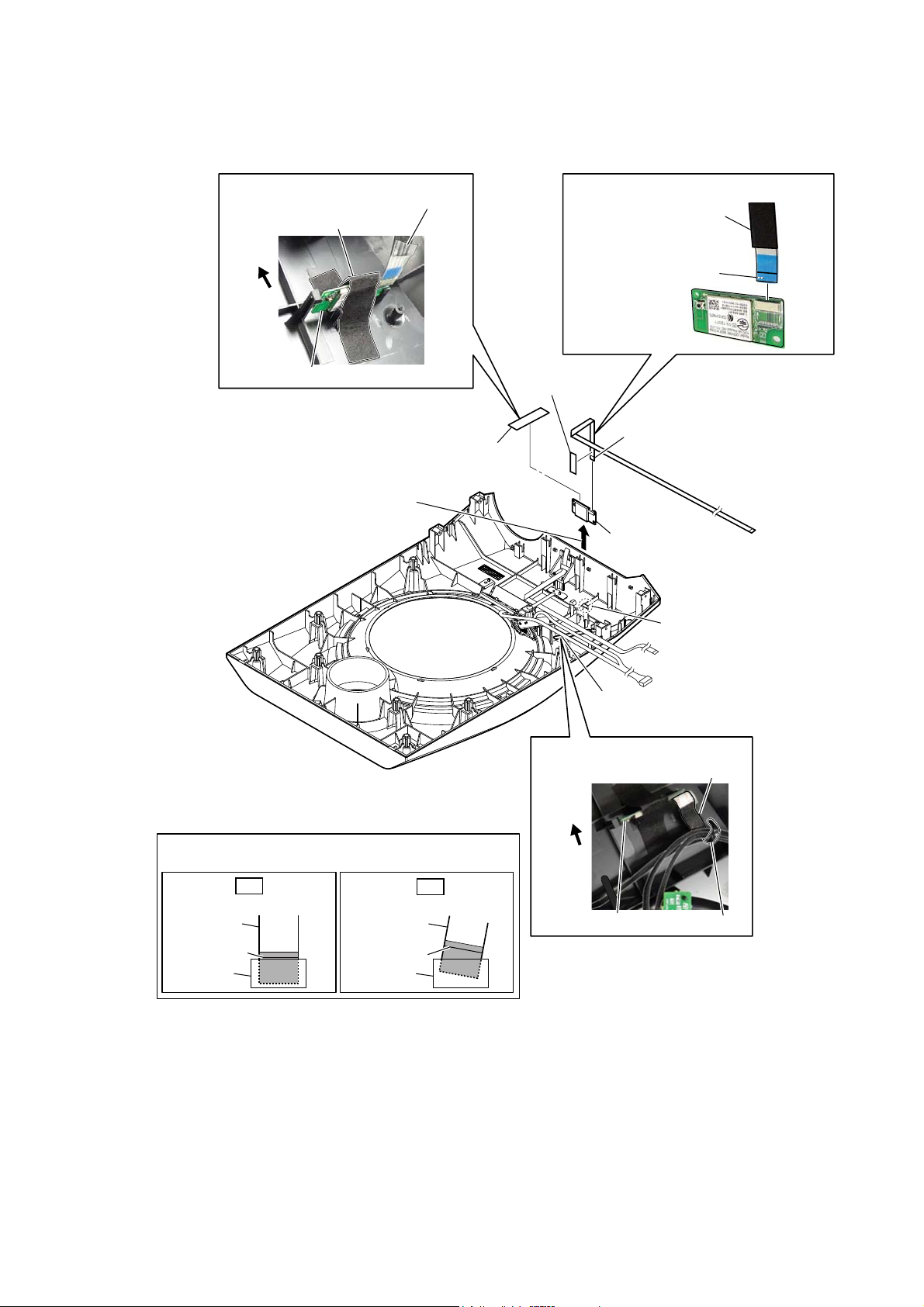
2-6. BLUETOOTH MODULE (BT1)
HT-GT1
:LUHVHWWLQJ
flexible flat cable (14P)
saranet cushion (15T50)
top side
bluetooth module
Remove the
4
in the direction of the arrow.
bluetooth module block
2 saranet cushion
(15T50)
+RZWRLQVWDOOWKHIOH[LEOHIODWFDEOH3
flexible flat cable (14P)
The lower side is
the terminal side.
5 filament tape
(sub material)
6 flexible flat cable (14P)
(FFC4)
7 bluetooth module
(BT1)
3 claw
–)URQWSDQHOEORFNUHDUERWWRPYLHZ–
When installing the flexible flat cable, ensure that
Note:
the colored line is parallel to the connector after insertion.
OK
Insert straight into the interior.
flexible flat
cable
colored line
connector
flexible flat
cable
colored line
connector
NG
Insert at a slant.
1 Remove the wire
from the clamp.
:LUHVHWWLQJ
flexible flat cable (14P)
top side
bluetooth module
clamp
11
Page 12
HT-GT1
2-7. PANEL BOARD BLOCK
1 Remove the wire
from the clamp.
– Top panel block rear bottom view –
3 clamp
5 connector
(CN301)
2 screw
(BVTP2.6)
6 PANEL board block
:LUHVHWWLQJ
clamp
2 screw
(BVTP2.6)
BUTTON board
PANEL board
Lift up the
4
in the direction of the arrow.
PANEL board block
12
Page 13
2-8. BUTTON ASSY
– Top panel block rear bottom view –
1 two screws
(BVTP2.6)
2 USB board
6
in the direction of the arrow.
3 Remove the wire
from the clamp.
8 BUTTON board block
Lift up the
BUTTON board block
:ire VettinJ
HT-GT1
VOL board
clamp
Do not touching to
Note:
top panel assy.
top panel assy
4 four screws
(BVTP2.6)
4 screw
(BVTP2.6)
5 clamp
7 connector
(CN302)
9 seven screws
(BVTP2.6)
0 BUTTON board block
qd button assy
qa saranet cushion (7T25)
qs saranet cushion (7T25)
qa saranet cushion (7T25)
qa saranet cushion (7T25)
,nVtallation poVition oI tKe Varanet cXVKion T
button assy
guide line
guide line
saranet cushion
(7T25)
saranet cushion
(7T25)
saranet cushion
(7T25)
saranet cushion
(7T25)
guide line
13
Page 14

HT-GT1
2-9. KNOB ASSY
+RZWRLQVWDOOWKHNQREDVV\
When installing the knob assy, aline the two ribs of knob assy and the shaft.
Note:
1 eight screws
(BVTP2.6)
3 VOL board block
– Bottom view – – Top view –
knob assy
rib
shaft
4 Draw the knob assy in
the direction of the arrow.
5 knob assy
VOL board block
– Top panel block rear bottom view –
2 Remove the VOL board block
in the direction of the arrow.
14
Page 15
2-10. TOP PANEL ASSY
HT-GT1
2 PEF cushion
(7T100)
2 PEF cushion
(7T100)
1 PEF cushion
(7T100)
3 saranet cushion
(15T50)
1 PEF cushion
(7T100)
– Top panel block rear bottom view –
4 saranet cushion
(15T50)
4 saranet cushion
(15T50)
4 saranet cushion
(15T50)
4 saranet cushion
(15T50)
5 top panel assy
3 saranet cushion
(15T50)
15
Page 16
HT-GT1
2-11. REAR PANEL BLOCK
:ire VeWWiQJ
MAIN board
rear
side
Rear panel block
CN4003
clamp
When installing the flexible flat cable, ensure that
Note:
the colored line is parallel to the connector after insertion.
OK
Insert straight into the interior.
flexible flat
cable
colored line
connector
flexible flat
cable
colored line
connector
2 Remove the wire
from the clamp.
NG
Insert at a slant.
5 Remove the rear panel block
in the direction of the arrow.
6 flexible flat cable (9P)
(CN3006)
7 rear panel
block
4 eight screws
(BVTP3 u 8)
4 five screws
(BVTP3 u 8)
3 connector
(CN4003)
– Rear view –
1 Draw the cord bushing
out of the groove.
16
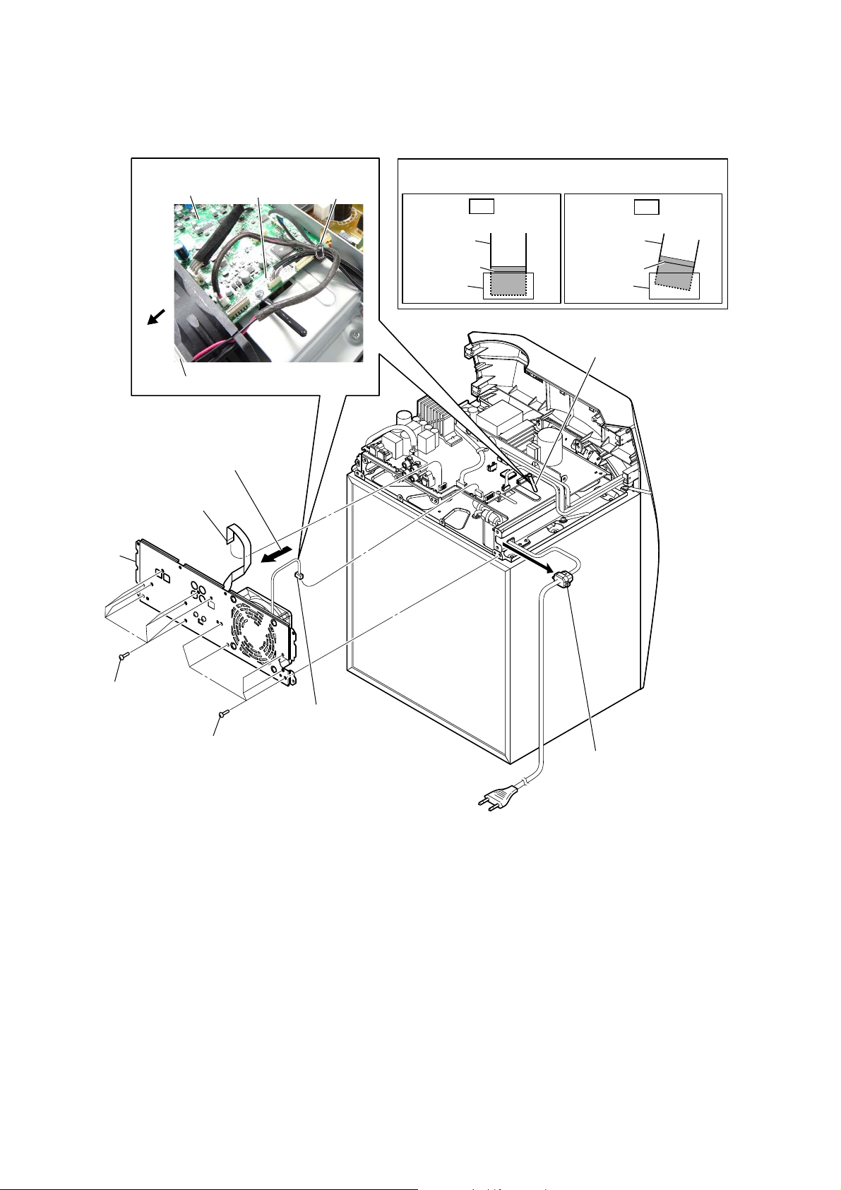
Page 17
2-12. DC FAN (M1)
2 EVA cushion (20T50)
HT-GT1
1 four screws
(BVTP3 u 8)
3 DC fan (M1)
2-13. TUNER BOARD
6 plate (top) shield
1 filament tape
(sub material)
2 flexible flat cable (9P)
(CN802)
5 plate (bottom) shield
4 filament tape
(sub material)
3 two screws
(BVTP3 u 8)
7 TUNER board
When installing the flexible flat cable, ensure that
Note:
the colored line is parallel to the connector after insertion.
OK
Insert straight into the interior.
flexible flat
cable
colored line
connector
flexible flat
cable
colored line
connector
NG
Insert at a slant.
17
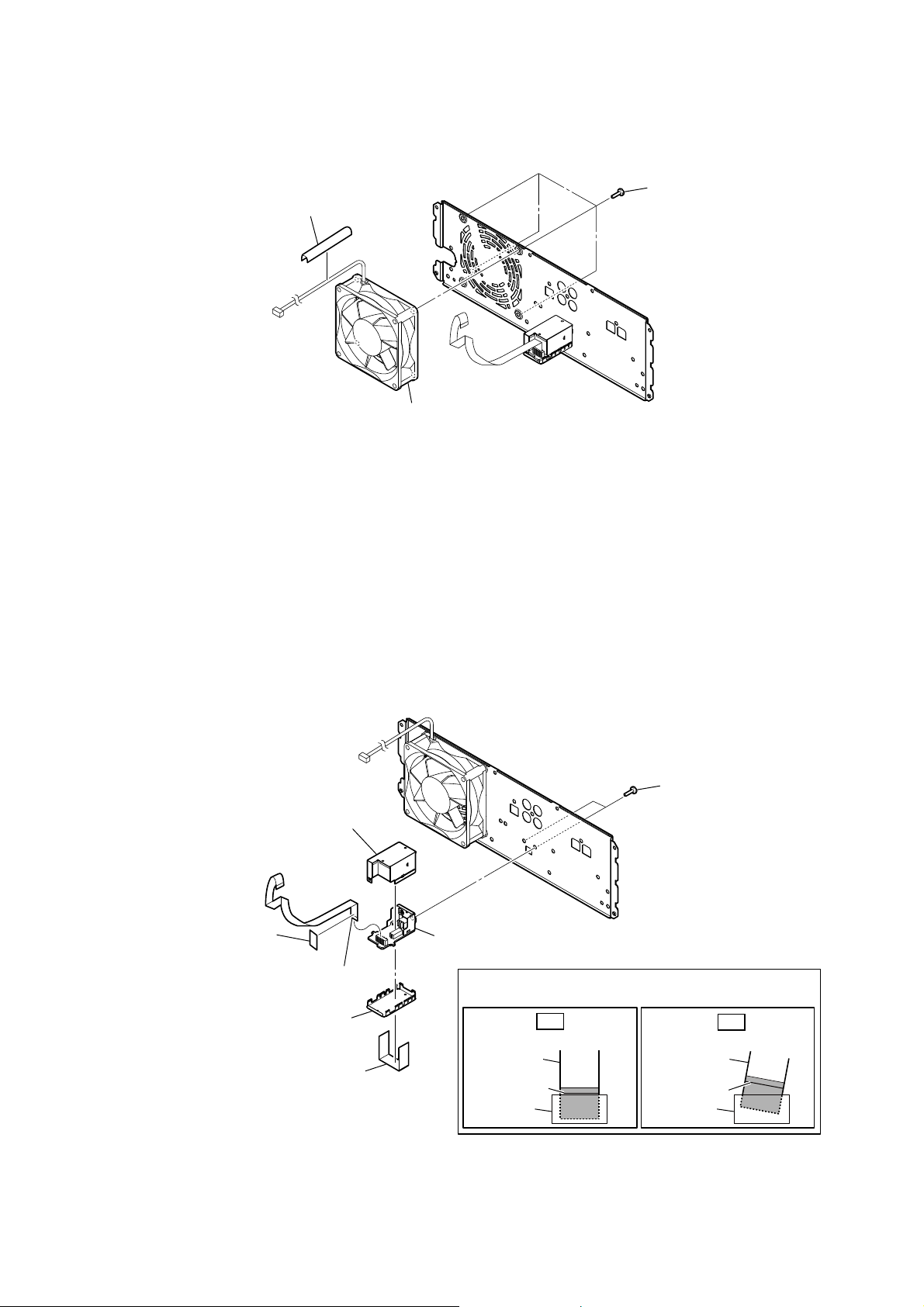
Page 18
HT-GT1
2-14. MAIN BOARD-1
• Continued on 2-15 (page 19).
:LUHVHWWLQJ
MAIN board
rear side
MAIN board
CN2001
CN2001
1 Remove the wire
from the clamp.
3 flexible flat cable (8P)
(CN3002)
2 connector
(CN2001)
4 flexible flat cable (14P)
(CN3003)
5 connector
(CN3005)
clamp
When installing the flexible flat cable, ensure that
Note:
the colored line is parallel to the connector after insertion.
OK
Insert straight into the interior.
flexible flat
cable
colored line
connector
rear side
NG
Insert at a slant.
flexible flat
cable
colored line
connector
–5HDUYLHZ–
18
Page 19
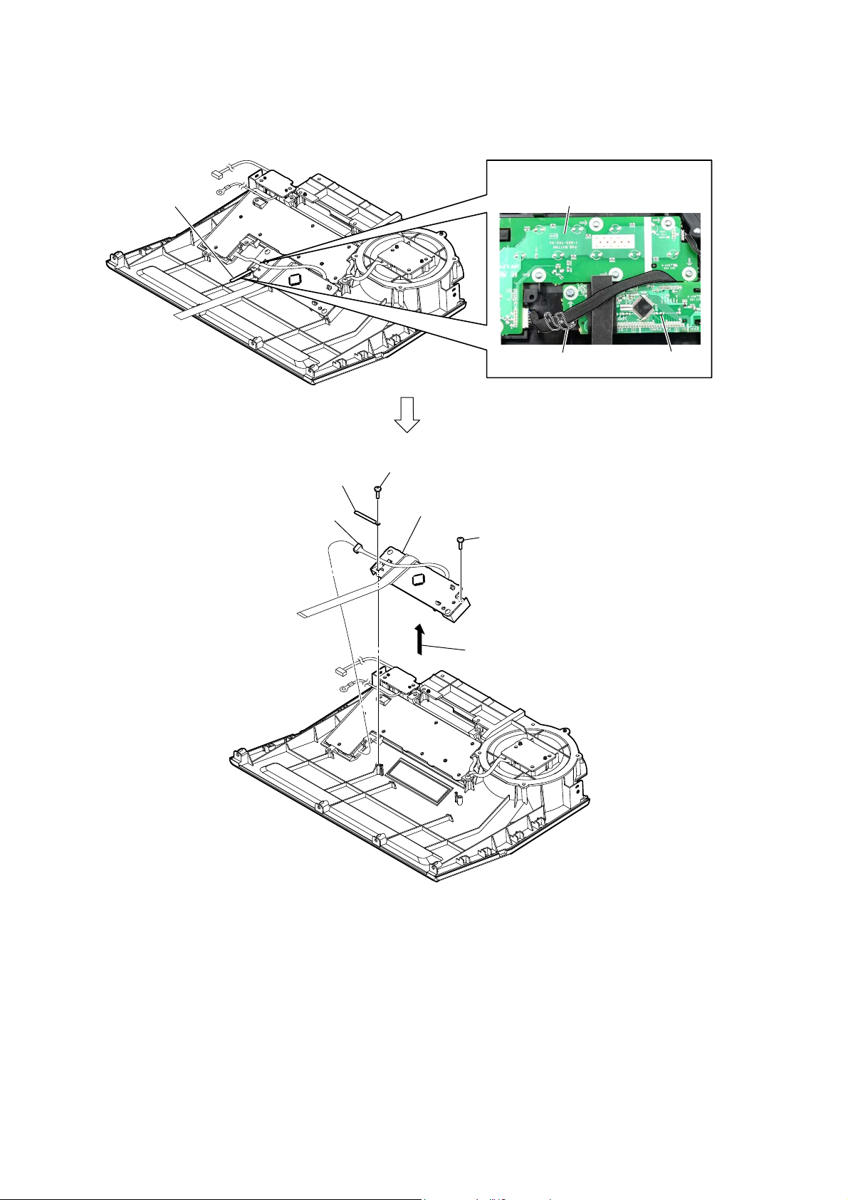
2-15. MAIN BOARD-2
HT-GT1
4 screw (BV3)
5 clamp
4 screw (BV3)
2 connector
(CN4002)
1 Remove the wire
from the clamp.
4 screw
(BV3)
8 AMP heatsink
4 two screws
(BV3)
:LUHVHWWLQJ
clamp
CN4002
rear side
MAIN board
5 clamp
4 screw (BV3)
5 clamp
7 two screws
(BV3)
9 MAIN board
3 connector
(CN4001)
6 Remove the MAIN board block
in the direction of the arrow.
19
Page 20
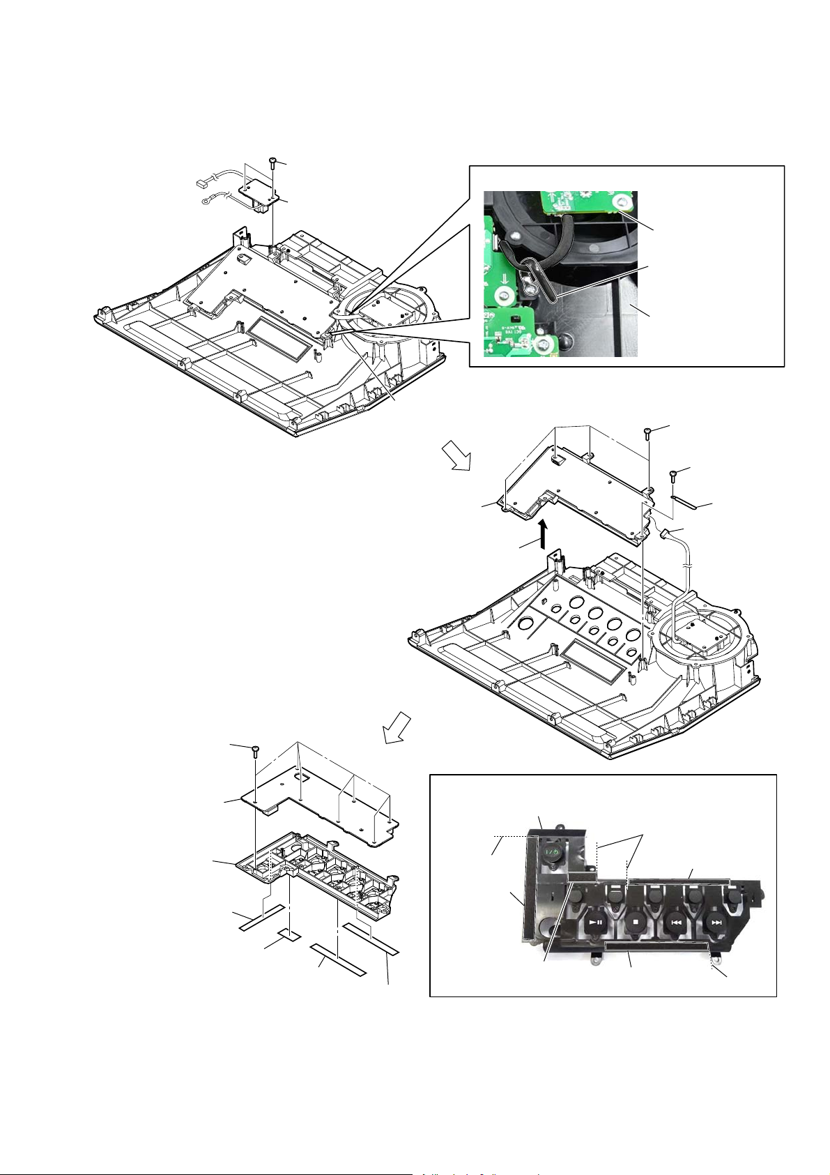
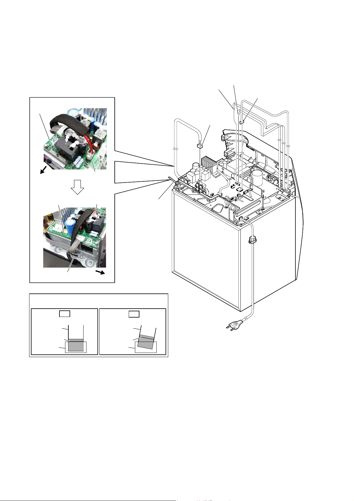
HT-GT1
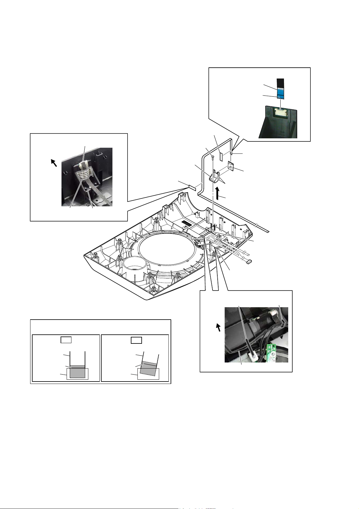
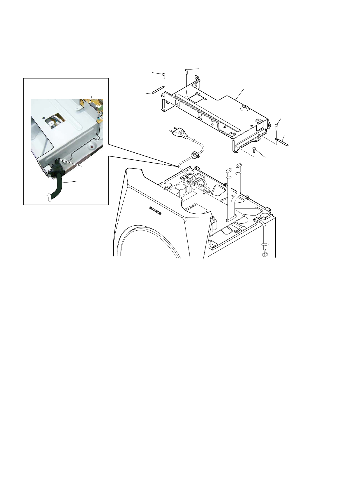
2-16. SUB CHASSIS
3RZHUFRUGVHWWLQJ
sub chassis
groove
power cord
1 screw
(BV3)
2 clamp
1 screw
(BV3)
3 sub chassis
1 screw
(BV3)
2 clamp
1 screw
(BV3)
20
Page 21
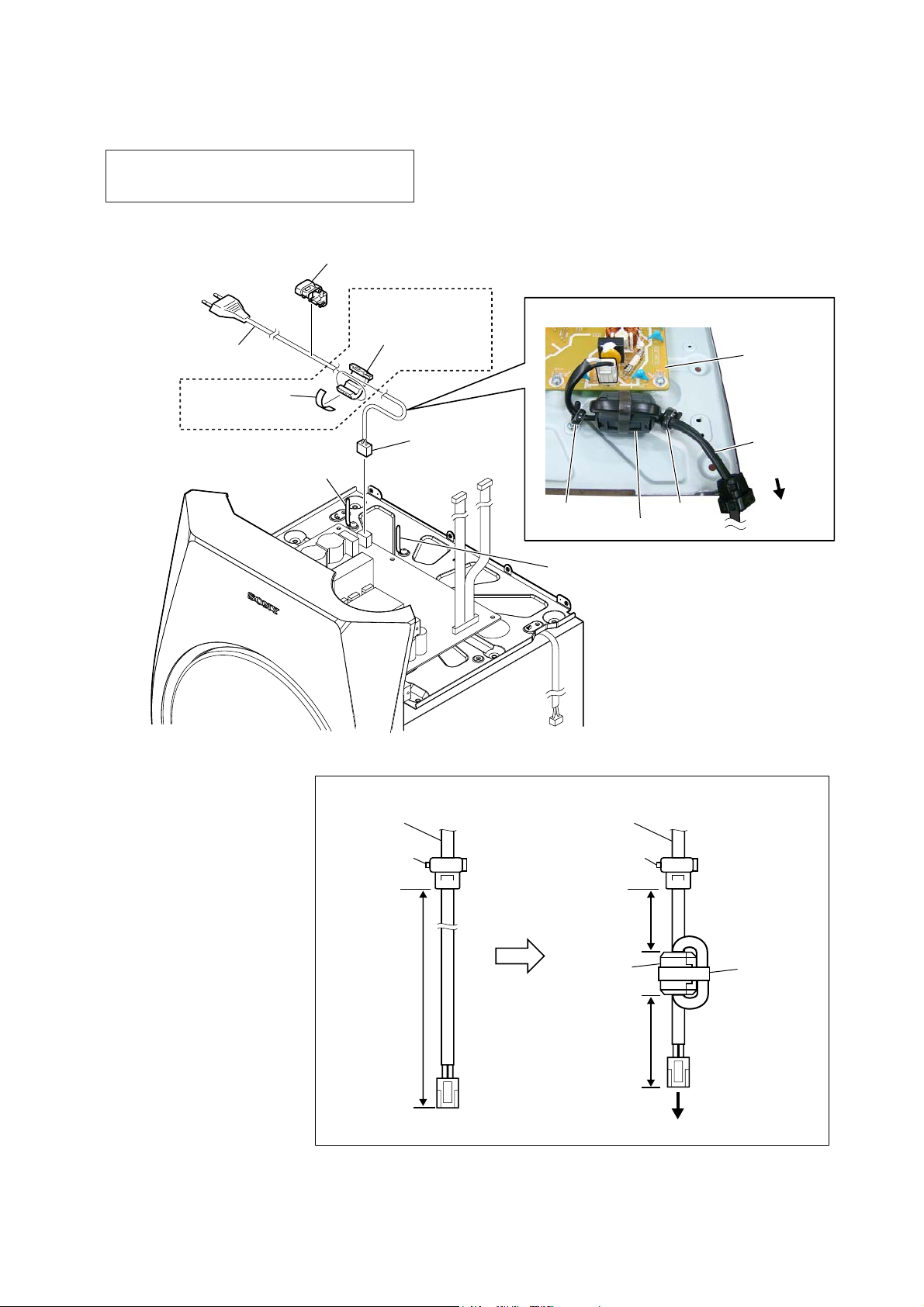
2-17. POWER CORD (AC1)
Note: Ferrite core (Ref. No. FC1) and PEF cushion (T100)
are deleted from the midway of production.
(E3, E12, E32, E51, MX, BR, SP)
5 cord bushing
(FBS001)
HT-GT1
Ver. 1.1
6 power cord
(AC1)
3 PEF cushion
(T100)
1 Remove the wire
from the clamp.
86$(3588.
$86($
4 ferrite core
(FC1)
2 connector
(CN100)
3RZHUFRUGVHWWLQJ
ferrite core
1 Remove the wire
from the clamp.
SMPS board
power cord
clampclamp
rear side
+RZWRLQVWDOOWKHFRUGEXVKLQJ)%6DQGWKHIHUULWHFRUH
power cord
cord bushing
(FBS001)
265 +5, -0 mm
power cord
cord bushing
(FBS001)
70 +5, -0 mm
ferrite core
60 +5, -0 mm
to SMPS board
PEF cushion
(T100)
21
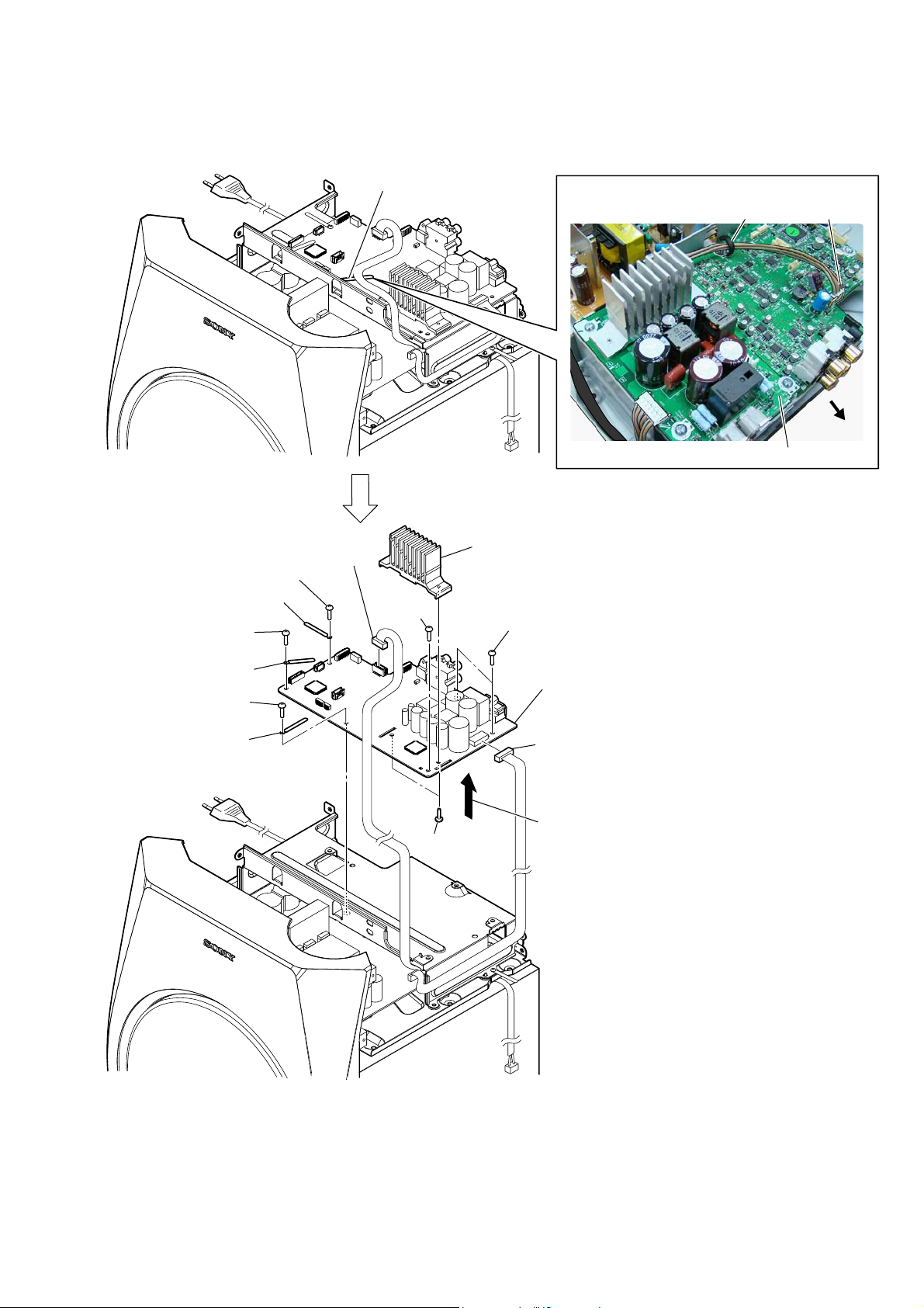
Page 22
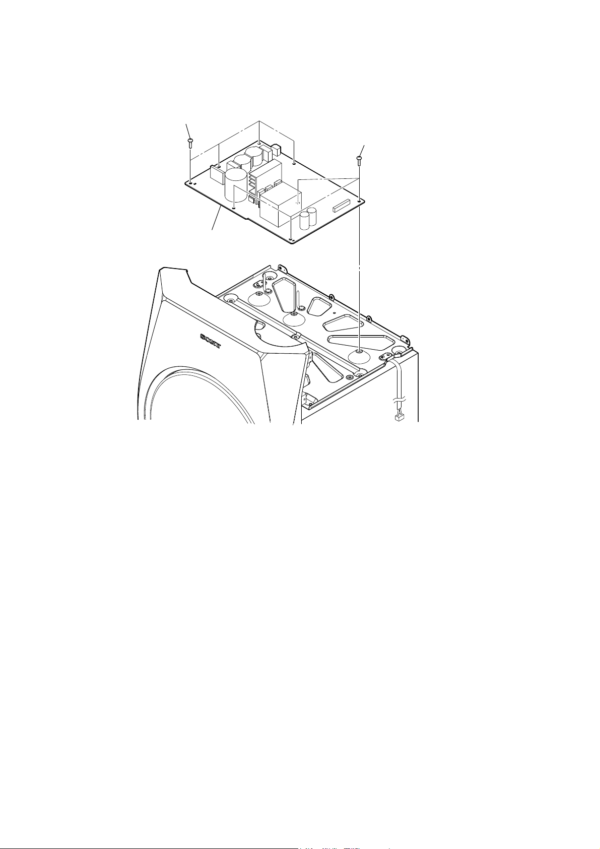
HT-GT1
2-18. SMPS BOARD
1 four screws
(BV3)
1 four screws
(BV3)
2 SMPS board
22
Page 23

2-19. LOUDSPEAKER (18 cm) (SP1)
,QVWDOODWLRQGLUHFWLRQIRUWKHORXGVSHDNHUFP
loudspeaker (18 cm)
4 loudspeaker (18 cm)
(SP1)
terminal position
HT-GT1
1 six tapping screws
(3.5 u 14)
:LUHVHWWLQJ
terminal
(narrow side)
terminal
(wide side)
terminal
(narrow side)
terminal
(wide side)
protrusion
protrusion
2 Remove the loudspeaker (18 cm) (SP1)
in the direction of the arrow.
3 Push the protrusion,
and remove the terminal
(narrow side).
3 Push the protrusion,
and remove the terminal
(wide side).
23
Page 24

HT-GT1
2-20. SERVICE POSITION
top panel block
MAIN board
insulating sheet
stand
24
Page 25

SECTION 3
TEST MODE
HT-GT1
1. TEST MODES OTHER THAN THE TEST MODE
MENU
These are executable test mode even if not entering the test mode
menu.
1-1. User Reset
It can initialize various backup information.
Procedure:
1. Press the [
2. Press two buttons of the [FUNCTION] and [
ously for one second.
3. The message “RESET” is displayed on the liquid crystal display, then turn the power off.
1-2. Bluetooth Power Control
It can turn on or off the Bluetooth signal.
Procedure:
1. Press the [
2. Press the [FUNCTION] button to turn the Bluetooth function.
3. Press two buttons of the [u] and [BLUETOOTH PAIRING] simultaneously for three seconds.
4. The message “BT ON” or “BT OFF” is displayed on the liquid
crystal display, it turn on or off the Bluetooth signal.
] button to turn the power on.
?/1
Screen display
] button to turn the power on.
?/1
Screen display
] simultane-
?/1
2. TEST MODES IN THE TEST MODE MENU
These are the test modes done in the test mode menu.
Setting method of the test mode menu:
1. Press the [
2. Press the two buttons of the [
taneously for fi ve seconds.
3. The message “COLD RST” is displayed on the liquid crystal
display and enter the test mode menu.
Releasing method of the test mode menu:
Press the two buttons of the [u] and [PARTY CHAIN] simultaneously for fi ve seconds.
2-1. Cold Reset
It can initialize various backup information.
Procedure:
1. Enter the test mode menu. (Refer to “Setting method of the test
mode menu”)
2. Press the [
lect the “COLD RST”, press the [
3. The message “RESET” is displayed on the liquid crystal display, then turn the power off.
] button to turn the power on.
?/1
] and [P AR TY CHAIN] simul-
u
Screen display
– TUNING]/[> TUNING +] buttons to se-
.
] button.
u
Screen display
or
1-3. Bluetooth History Clear
It can clear the Bluetooth pairing history.
Procedure:
1. Press the [
2. Press the [FUNCTION] button to turn the Bluetooth function.
3. Press two buttons of the [x] and [BLUETOOTH P AIRING]
simultaneously for one second.
4. The message “BT HIST” → “CLEAR” is displayed on the
liquid crystal display, and the pairing history of Bluetooth is
cleared.
] button to turn the power on.
?/1
Screen display
25
Page 26

HT-GT1
2-2. Panel Test Mode
It can confi rm the lighting of liquid crystal display and LEDs, op-
eration of buttons, display of model name, destination and software version.
Procedure:
1. Enter the test mode menu. (Refer to “Setting method of the test
mode menu” on page 25)
2. Press the [
– TUNING]/[> TUNING +] buttons to se-
.
lect the “PNL TEST”, press the [u] button.
3. All segments in the liquid crystal display and all LEDs are
lighted up.
4. When pressing the [x] button, the display on the liquid crystal
display repeatedly changes in order from all lighting → pattern
1 (Bluetooth LED is lighted up) → pattern 2 (speaker LED is
lighted up) → all lighting → all turned off.
All lighting
REC
PRESET
c
SLEEP
N X
Pattern 1
SLEEP
N
Pattern 2
REC
c
AUTO MONO ST TUNED
AUTO MONO TUNED
PRESET
ST
SUBWOOFER BASS
BASS
SUBWOOFER
FLDR
SHUF
PGM
FLDR
PGM
SHUF
1
1
5. In the state of step 4, press the [> TUNING +] button and
model name “GV” is displayed on the liquid crystal display.
Screen display
Each time the [> TUNING +] button is pressed, the display
changes from destination → SC version → UI version→ PF
version → SYS version → MM version 1 → MM version 2 →
iPod version 1 → iPod version 2 → ST version → TA version
→ T AS version → TM version → BTM version → BT version
→ NFC version → PCT version in this order, and returns to the
model name display.
Model name
iPod version 2
Destination
ST version
SC version
TA version
UI version
TAS version
PF version
All lighting
REC
PRESET
c
SLEEP
N X
All turned off
AUTO MONO ST TUNED
SUBWOOFER BASS
FLDR
SHUF
PGM
TM version
SYS version
1
BTM version
MM version 1
BT version
MM version 2
NFC version
iPod version 1
PCT version
(Displayed values in the above fi gure are example)
6. When [FUNCTION] button is pressed while the each version
is displayed on the liquid crystal display, month and day of the
software creation is displayed on the liquid crystal display.
Screen display
26
(Displayed values in the above fi gure are example)
When [FUNCTION] button is pressed again, the display re-
turns to the each version display.
– Continued on next page –
Page 27

SECTION 4
ELECTRICAL CHECK
HT-GT1
7. When pressing the [. – TUNING] button, “K 0 V0” is displayed on the liquid crystal display.
Screen display
8. Each time a button is pressed, “K 0” value increases. However,
once a button is pressed, it is no longer taken into account.
When pressing the all buttons, “OK” and “K10” are alternately
displayed on the liquid crystal display.
Screen display
9. “V0” value increases “V0”, “V1”, “V2”, “V3”... if turn the
[VOLUME] knob clockwise, or it decreases “V0”, “V9”,
“V8”, “V7”... if turn the [VOLUME] knob counterclockwise.
Releasing method:
Press the two buttons of the [u] and [PARTY CHAIN] simultaneously for fi ve seconds.
TUNER SECTION
FM TUNE LEVEL CHECK
generator
Procedure:
1. Press the [?/1] button to turn the power on.
2. Input the following signal from signal generator to FM antenna
input directly.
Carrier frequency : A = 87.5 MHz, B = 98 MHz, C = 108 MHz
Deviation : 75 kHz
Modulation : 1 kHz
ANT input : 35 dBu (EMF)
Note: Use 75 ohm coaxial cable to connect signal generator and the unit.
You cannot use video cable for checking.
Use signal generator whose output impedance is 75 ohm.
3. Set to FM tuner function and tune A, B and C signals.
4. Confi rm “TUNED” is lit on the display for A, B and C signals.
When the selected station signal is received in good condition,
“TUNED” is displayed.
signal
0 dB = 1 V
unit
2-3. Factory Preset Mode
It can memorize specialized preset station for each destination of
FM preset.
Procedure:
1. Enter the test mode menu. (Refer to “Setting method of the test
mode menu” on page 25)
2. Press the [. – TUNING]/[> TUNING +] buttons to select the “FCT PSET”, press the [u] button.
3. The message “FACTORY” is displayed on the liquid crystal
display, FM preset station setting is complete.
Screen display
2-4. Safety Mode
(It is displayed “SAFETY” on the liquid crystal display)
Not used for the servicing.
2-5. NFC test Mode 1
(It is displayed “NFC TST1” on the liquid crystal display)
Not used for the servicing.
2-6. NFC test Mode 2
(It is displayed “NFC TST2” on the liquid crystal display)
Not used for the servicing.
27
Page 28

HT-GT1
1. When sound is not outputted
Sound is not outputted
Sound is not output from all
functions.
Yes
SECTION 5
TROUBLESHOOTING
The voltage of the following
pin is 36 V.
MAIN board: CN4001
Between the pin 1 (V1) and
pin 4 (V1_GND).
Yes
The voltage of the following
pin is “H”.
MAIN board: IC002
pin 2 (RESET)
Yes
Replace the IC002 on the
MAIN board.
No
Fuse (F100) on the SMPS
board conduct the electricity.
Replace the Q101 and Q103
on the SMPS board.
Check and repair the IC002
on the MAIN board and the
surrounding circuit.
2. When liquid crystal display is not displayed
Yes
NoNo
Replace the fuse (F100) on the
SMPS board.
Liquid crystal display is
not displayed
Display does not change when
you press the [DISPLAY] button
on the remote commander.
Yes
The liquid crystal display is
displayed, when pull out the
speaker cable (CN2001 (for
SP1) and TB003 (for SS-GT1)
on the MAIN board), and then
turn the AC power on/off again.
Yes
Replace check the wire
and speaker.
No
DC detection of IC002 is working.
Check the short-circuit (the power
source or the earth fault) of the
audio output line of the IC002.
Replace the IC002 if there is
no problem.
28
Page 29

6-1. BLOCK DIAGRAM - MAIN Section -
X1001
OPTICAL
RECEIVER
IC5005
22 USB_DP
21 USB_DM
15
XOUT_PLL
14
XIN_PLL
SDA
9
USB DECODER
IC1002
SCL
BUSY
8
7
OPT IN
CN701
5V 1A
3
D+
2
D–
16.9344MHz
SECTION 6
DIAGRAMS
X1003
24.576MHz
27DATA
26BCK
25LRCK
MCHNG
SEARCH
IRPTO
RESETX
6
5
4
2
DIGITAL AUDIO
INTERFACE RECEIVER
IC1006
31 RXIN4
40
XTO
39
XTI
MDI/SDA23MDO/ADR025MC/SCL26MS/ADR12ERROR/INT0
24
NPCM/INT134RST
1
HT-GT1
17DOUT
19BCK
18LRCK
AMP_DATA_LR,
AMP_DATA_SW,
AUDIOLINK_DATA,
AMP_BCK, AMP_MCK,
AMP_LRCK, BCK, DOUT
(Page 30)
>001B
BT_PCM_OUT
BT_PCM_CLK
DIGITAL AUDIO SELECTOR
IC1005
51C1
61C0
41C2
11 2C1
10 2C0
12 2C2
CLOCK SIGNAL SELECTOR
IC1009
71Y
92Y
A14B
2
SAMPLE RATE
CONVERTER
4SDIN
5BCKI
6 LRCKI
2 RCKI
IC1003
13
RST
BCK
DOUT
23SDOUT
25BCKO
24LRCKO
X1002
12.288MHz
12
SDIN2
11
SDIN1
22
SCLKOUT1
19
LRCK
4XTALO
3XTALI
32
AUDIO DSP
IC1008
RESET8GPIO14SDIN416SCL115SDA1
27SDOUT1
26SDOUT2
25SDOUT3
23SCLKOUT2
21MCLKO
AMP_DATA_LR
AMP_DATA_SW
AUDIOLINK_DATA
AMP_BCK
AMP_MCK
AMP_LRCK
BT1
Bluetooth
MODULE
PCM_OUT
PCM_CLK
PCM_SYNC
UART_TX
UART_RX
UART_RTS
UART_CTS
MUTE
RESET
BT_PCM_OUT
BT_PCM_CLK
BT_PCM_SYNC
75
76
77
USB SCL
USB SDA
BLUETOOTH RXD
34
BLUETOOTH TXD
33
BLUETOOTH CTS
32
BLUETOOTH RTS
36
BLUETOOTH MUTE
18
BLUETOOTH RESET
35
73
79
USB BUSY
USB MCHNG
74
78
USB IRPTO
USB RESET
USB SEARCH
54
55 56
DIR_DOUT
52
DIR_DIN
DIR_CLK
57
DIR_CS
DIR_FLAG158DIR_FLAG2
53
DIR_RESET
BT_PCM_SYNC
89
83
DSEL
EXT_SEL_D-A
51C1
61C0
41C2
A14B
2
SYSTEM CONTROLLER
IC3001 (1/3)
71Y
EEPROM
IC3002
SDA6SCL7RST
2
22
CP IIC SDA
20
CP IIC CLK
23
CP RESET
11
X3001
8MHz
Xout
X3002
32.768kHz
43
65
42
46
DSP INT
DSP RESET
DSP MUTE
45
DSP IIC_CLK
DSP IIC_SDA
13
Xin
9
Xcout
8
XcIN
SIGNAL PATH
: AUDIO (DIGITAL)
: USB
: Bluetooth
HT-GT1
2929
Page 30

HT-GT1
6-2. BLOCK DIAGRAM - AMP Section -
AMP_DATA_LR,
AMP_DATA_SW,
AUDIOLINK_DATA,
AMP_BCK, AMP_MCK,
AMP_LRCK, BCK, DOUT
>001B
(Page 29)
AMP_DATA_LR
AMP_BCK
AMP_LRCK
AMP_MCK
AMP_DATA_SW
AMP_BCK
AMP_LRCK
AMP_MCK
AUDIOLINK_DATA
AMP_BCK
AMP_LRCK
AMP_MCK
D/A CONVERTER
IC004
2
DATA
1
BCK
3
LRCK
16 SCK
D/A CONVERTER
IC005
2
DATA
1
BCK
3
LRCK
16
SCK
D/A CONVERTER
IC5003
2
DATA
1
BCK
3
LRCK
16
SCK
POWER AMP
IC002
7VOUTL
8VOUTR
7VOUTL
8VOUTR
7VOUTL
8VOUTR
R-CH
DAC LPF
IC006
DAC LPF
IC007
LINE AMP
IC5004
PRE AMP
IC003
PRE AMP
IC001
10 INPUT_C
11 INPUT_D
5 INPUT_B
4 INPUT_A
15SD2
RESET
36OUT_C_36
37OUT_C_37
28OUT_D_28
29OUT_D_29
OVER LOAD
DETECT
Q004, 005
44OUT_B_44
45OUT_B_45
52OUT_A_52
53OUT_A_53
OVER LOAD
DETECT
Q006, 007
OVER LOAD
DETECT
Q002, 003
–2
–1
RY001
RELAY DRIVE
Q008
TB003
+
–
–
+
L
SPEAKERS
FRONT
R
SP1
(SUBWOOFER)
ANTENNA
FM
TUNER BOARD
TUNER_SDA_UCOM
TUNER_SCL_UCOM
AUDIO IN
PARTY CHAIN IN
LOUT
ROUT
TUNER_OE
RDS_INT
J5001 (1/2)
L
R
R-CH
TUNER_SDA_UCOM
TUNER_SCL_UCOM
TUNER_OE
RDS_INT
R-CH
TUNER_SCL_UCOM
TUNER_SDA_UCOM
RDS_INT
TUNER_OE
LINK BIAS
DETECT
Q5003, 5004
ANALOG AUDIO
SELECTOR
IC1007
12Y0
52Y1
DOUT
A/D CONVERTER
IC1004
32-COM
A
10
ANALOG AUDIO
SELECTOR
IC5001
Q1001
12Y0
42Y3
INVERTER
10 9
Q5006
32-COM
AB
R-CH
BCK
AMP_LRCK
AMP_MCK
LINE AMP
IC5002
R-CH
13
14
8
7
6
MUTING
Q5002, 5005
VINL
VINR
BCK
LRCK
SCKI
DOUT
9
J5001 (2/2)
L
PARTY CHAIN OUT
R
AUDIO OUT
DC DETECT
Q012
PROTECT_DET
>002B
(Page 31)
R-ch is omitted due to same as L-ch.
SIGNAL PATH
: AUDIO (ANALOG)
: AUDIO (DIGITAL)
: TUNER
MUTING
CONTROL
Q5007
LINK BIAS
CONTROL
Q5001
: AUDIO IN
HT-GT1
27
28
TUNER SCL
TUNER SDA
25
72
TUNER ON
RDS-INT
16
I-BIAS DETECT
40
EXT SEL_A
19
38
O_LINK_A
O_LINK_B
41
O-LINK MUTE (LINK)
21
O-BIAS
SYSTEM CONTROLLER
IC3001 (2/3)
3030
50
47
DAMP_RESET
PROTECT_DET
87
DC-OFFSET
82
F_SPK_RELAY
Page 31

6-3. BLOCK DIAGRAM - PANEL/POWER SUPPLY Section -
HT-GT1
ND401
LIQUID
CRYSTAL
DISPLAY
D401
(LCD BACK LIGHT)
D301
BLUETOOTH
PAIRING
D911
SPEAKER
ILLUMINATION
S304 – 307, 309
(TOP PANEL KEYS)
S301 – 303, 308, 310
(TOP PANEL KEYS)
M1
(FAN)
EN501
VOLUME
M
REMOTE CONTROL
LCD DRIVER
IC401
COM0 – COM3
LED DRIVE
Q401
LED DRIVE
Q3007, 3008
LED DRIVE
Q3013, 3015
ROTARY
ENCODER
NFC1
NFC MODULE
(RC-S801)
FAN MOTOR
CONTROL
Q4003, 4007
RECEIVER
DATA
CLK
IRQ
Standby
SEL
RF-DET
IC601
5
SIRCS
SWITCHING
Q4006
PVDD
D4010
D4017
D4013
D4014
PROTECT
DETECT
Q4010
DC/DC
CONVERTER
IC4004
REGULATOR
Q4001, 4002, 4005
VOLTAGE
DETECT
IC4003
D4019
D4018
D4012
D4015
D1026, 1027
POWER VOLTAGE
CONTROL
Q1003, 1004
PROTECT
DETECT
Q4008, 4009
D1021
SHUNT
REGULATOR
IC1858
PROTECT
DETECT
Q1001, 1002
D1007
D1006
ISOLATOR
PH100
ISOLATOR
PH101
D116
RECT
D1010
PROTECT_DET
OVER LOAD
PROTECT
Q109, 110, 112, 113
SWITCHING
Q111
SWITCHING
Q114
REGULATOR
Q115
T100
POWER
TRANSFORMER
(Page 30)
>002B
D114
D109, 108
D124 D121 D119
D122
RECT
D113
POWER ON/OFF
CONTROL
Q101, 103, 106, 107
TH101
POWER CONTROL
3
OLP
4
FB
2
VCC
OCP1BD5
7
OCP2
8
DRIVE
LINE FILTER
L100, 102
IC100
F100
AC1
(AC IN)
10SEG0 – SEG31 SDA
9SCL
8CSB
13INHB
7OSC
99 DP SDA
100 DP SCL
95 DP CS
98 DP INH
24 DP DRV CLK
SYSTEM CONTROLLER
IC3001 (3/3)
59 BLUETOOTH_LED
26 LED_RED
90 KEY 1
91 KEY 2
92
VOLUME-JOG
67 NFC DATA
68 NFC CLOCK
69 NFC IRQ
63 NFC STANDBY
64 NFC DATA SEL
66 NFC RF DETECT
71 FAN_SPEED
USB POWER 80
USB OVERCURRENT
PROTECT
PVDD-ON
P-ON
BLUETOOTH ON
AC-CUT
VBUS
81
D5.2V
D3.3V
48
CNETER
VOLTAGE
AMP B+
88
AVDD+5V
84
37
17
+12V
BT3.3V
E3.3V
BTLED_POWER
VBUS
SWITCH
IC1001
CENTER VOLTAGE
GENERATOR
Q5009
B+ SWITCH
Q3001, 3002
DC/DC CONVERTER
3
SW1
14
SW2
5
EN1
B+ SWITCH
Q5008
+5V
REGULATOR
IC4005
+3.3V
REGULATOR
IC4002
IC4001
VIN1 1
VIN2 16
D4007
D4008
HT-GT1
3131
Page 32

HT-GT1
THIS NOTE IS COMMON FOR PRINTED WIRING BOARDS AND SCHEMATIC DIAGRAMS.
(In addition to this, the necessary note is printed in each block.)
For Printed Wiring Boards.
Note:
• X : Parts extracted from the component side.
• Y : Parts extracted from the conductor side.
• : Pattern from the side which enables seeing.
(The other layers’ patterns are not indicated.)
Caution:
Pattern face side:
(Conductor Side)
Parts face side:
(Component Side)
Caution:
Pattern face side:
(SIDE B)
Parts face side:
(SIDE A)
• Indication of transistor.
C
Q
B
E
Note: When the complete MAIN board is replaced, refer to
“NOTE OF REPLACING THE IC002 ON THE MAIN
BOARD AND THE COMPLETE MAIN BOARD” on
page 5.
Parts on the pattern face side seen
from the pattern face are indicated.
Parts on the parts face side seen from
the parts face are indicated.
Parts on the pattern face side seen
from the pattern face are indicated.
Parts on the parts face side seen from
the parts face are indicated.
These are omitted.
For Schematic Diagrams.
Note:
• All capacitors are in μF unless otherwise noted. (p: pF) 50
WV or less are not indicated except for electrolytics and
tantalums.
• All resistors are in Ω and 1/4 W or less unless otherwise
specifi ed.
• 2 : Nonfl ammable resistor.
• 5 : Fusible resistor.
• C : Panel designation.
Note: The components identifi ed by mark 0 or dotted
line with mark 0 are critical for safety.
Replace only with part number specifi ed.
• A : B+ Line.
• Voltages and waveforms are dc with respect to ground
under no-signal (detuned) conditions.
no mark : TUNER (FM)
* : Impossible to measure
• Voltages are taken with VOM (Input impedance 10 M).
Voltage variations may be noted due to normal production
tolerances.
• Waveforms are taken with a oscilloscope.
Voltage variations may be noted due to normal production
tolerances.
• Circled numbers refer to waveforms.
• Signal path.
F : AUDIO (ANALOG)
J : AUDIO (DIGITAL)
f : TUNER
L : AUDIO IN
E : USB
a : Bluetooth
Note: When the complete MAIN board is replaced, refer to
“NOTE OF REPLACING THE IC002 ON THE MAIN
BOARD AND THE COMPLETE MAIN BOARD” on
page 5.
• Circuit Boards Location
NFC module
(RC-S801) (NFC1)
Bluetooth module
(BT1)
SPK-LED-H-L board
IR board
BUTTON board
USB board
PANEL board
TUNER board
MAIN board
SMPS board
VOL board
HT-GT1
3232
Page 33

HT-GT1
6-4. SCHEMA TIC DIAGRAM - MAIN Section (1/5) -
A
B
C
(Page 36)
D
E
F
G
H
I
J
K
L
M
N
>101S
MAIN
BOARD
(4/5)
(Page 36)
>102S
MAIN
BOARD
(4/5)
>103S
MAIN
BOARD
(Page 35)
>01S
USB
BOARD
CN702
(Page 41)
>104S
(Page 37)
>105S
MAIN
BOARD
(4/5)
(Page 36)
(3/5)
MAIN
BOARD
(5/5)
BT_PCM_OUT
BT_PCM_SYNC
BT_PCM_CLK
DIR_DIN
DIR_DOUT
DIR_RESET
DIR_CLK
DIR_ERR
DIR_NPCM
USB_IP_OCP
USB_MCHNG
USB_SEARCH
2
MAIN BOARD (1/5)
D3.3V
DIR_CS
D3.3V
OPTIN
DGND
CN1001
4P
CL1035
VBUS 1
CL1036
D– 2
CL1037
D+ 3
USB_ON
CL1038
D3.3V
D5.2V
DGND
AGND
DGND
VBUS GND 4
AVDD+5V
USB_SDA
USB_SCL
USB_BUSY
USB_IRPTO
USB_RST
FL1003
10R1092
C1074
0.01
C1059
47p
C1077
0.1
USB_SDA
USB_SCL
USB_BUSY
USB_MCHNG
USB_IRPTO
USB_RST
USB_SEARCH
3
45 7 1989
5
CL1061
3.3
20
21
22
DVDD
SCKO
DGND
IC1006
DIGITAL AUDIO
INTERFACE RECEIVER
PCM9211PTR
XTI39XTO40AGND41VCC42FILT
1.7
1.7
4700p
C1067
IC1001
FL1001
4
1.6
1.6
0
17
18
19
BCK
LRCK
IC1006
43
0
3.3
680
R1081
0.068
C1068
OUT
ILIM
FAULT
C1063
C1064
C1076
0.1
10
100R1094
R1091
10
10R1093
0.1
3.3
1.3
23
24
MDI/SDA
3.3
MC/SCL
25
3.3
MS/ADR1
26
3.3
MODE
27
RXIN7
28
RXIN6
29
RXIN5
30
3.3
RXIN4
31
RXIN3
32
RXIN2
33
3.3
RST
34
RXIN1
35
3.3
VDDRX
36
MDO/ADR0
RXIN037GNDRX
38
6
R1080
1M
C1065
10p
C1009
X1003
24.576MHz
1
R1079
100
C1066
12p
5.2
IN
1
GND
2
3.3
EN
3
IC1001
C1044
100p
VBUS SWITCH
TPS2553DBVR
• See page 42 for Waveforms. • See page 46 for IC Block Diagrams. • See page 50 for IC Pin Function Description.
R1076
100
R1077
100
R1078
100
16
14
DOUT
MPO015MPO1
VCOM44AGNDAD45VCCAD46VINL47VINR
48
0
0
4.9
C1070
100p
5.1
6
0.3
5
3.3
4
R1062
R1063
22k
R1006
10k
R1007
10k
6
R11010R1102
MPIO_B213MPIO_B3
MPIO_B1
12
MPIO_B0
11
MPIO_C3
10
MPIO_C2
9
MPIO_C1
8
MPIO_C0
7
MPIO_A3
6
MPIO_A2
5
MPIO_A1
4
MPIO_A0
3
0
NPCM/INT1
2
3.3
ERROR/INT0
1
C1071
100p
R1013
0
C1069
0.1
C1010
0.1
0
C1011
10
C1008
10
CL1022
CL1023
CL1024
3
CL1034
3.301.60001.6
28
29
30
AMUTE
31
DAVSS
32
RDACO
33
1.4
VCDACO
34
LDACO
35
3.3
DAVDD
36
3.3
SD_CON
37
3.3
SD_DO
38
SD_CLK
39
SD_DI
40
SD_CS
DVDDIO_29
DVSSIO_11RESETX2TMODE3IRPTO4SEARCH5MCHNG6BUSY7SCL8SDA9DVDD_M
3.3
CL1005
C1075
0.1
10R1095
USB_RST
100R1009
100R1008
26
27
DATA
MCLK
IC1002
USB DECODER
IC1002
BU94502AMUV
000
100R1003
100R1004
USB_IRPTO
USB_SEARCH
10R1048
10R1041
100R1040
25
BCK
LRCK
100R1084
USB_MCHNG
R1049
10
C1046
10p
24
0
10R1098
USB_BUSY
12kR1012
CLK24MI
10R1096
0
23
3.3
USB_SCL
100R1042
REXTI
R1052
10R1051
10R1050
R1044
4.7R1010
22
3.2
10R1097
USB_SDA
10
100
USB_DP
IC1005
DIGITAL AUDIO SELECTOR
TC74VHC153FT(EL)
1
1G
2
0
B
3
1C3
4
0
1C2
5
0
1C1
6
0
1C0
7
0
1Y
8
GND
IC1009
CLOCK SIGNAL SELECTOR
TC74VHC153FT(EL)
1
1G
2
0
B
3
1C3
4
0
1C2
5
1.6
1C1
6
1.6
1C0
7
1.6
1Y
8
GND
4.7R1011
2
21
USB_DM
20
AVSSC
3.3
19
AVDDC
18
SEL_SLAVE
3.3
17
TEST3
3.3
16
TEST2
1.4
15
XOUT_PLL
1.3
14
XIN_PLL
13
TEST1
3.3
12
DVDDIO_12
11
DVSSIO_11
10
0
C1005
0.1
10 11 12 13 14
R1103
0
IC1005
VCC
2C3
2C2
2C1
2C0
IC1009
VCC
2C3
2C2
2C1
2C0
CL1003
CL1002
R105310R1054
10
16
3.3
15
2G
14
0
A
13
12
0
11
1.6
10
1.6
9
1.6
2Y
16
3.3
15
3.3
2G
14
0
A
13
12
11
10
9
2Y
R1001
R1043
100
C1040
0.1
10R1055
1k
X1001
16.9344MHz
1
R1002
1M
C1042
C1057
C1072
C1073
0.1
0.1
0.1
50V
R1056
0
10R1057
10R1045
10R1046
R1058
0
LTC014EUBFS8TL
Q1001
INVERTER
3.3
1.7
0
1.6
1.6
3.3
3.3
3.3
0
R1014
10k
C1013
4.7
R1047
10
C1043
0.01
JL1003
C1041
R1090
0.1
100
C1035
0.1
C1007
0.1
C1004
0.1
C1003
0.1
C1001
10p
C1002
10p
C1031
0.1
10
IC1003
SAMPLE RATE CONVERTER
1
LGRP
2
RCKI
3
NC
4
SDIN
5
BCKI
6
LRCKI
7
VIO
8
DGND_8
9
BYPAS
10
IFMT0
11
IFMT1
12
IFMT2
13
RST
14
MUTE
R1018
1k
0
R1015
100k
R1017
1k
IC1003
SRC4182
JL1002
28
MODE2
27
MODE1
26
MODE0
25
1.6
BCKO
24
1.6
LRCKO
23
0.3
SDOUT
22
3.3
VDD
21
DGND_21
20
TDMI
19
3.3
OFMT0
18
OFMT1
17
OWL0
16
OWL1
15
0
RDY
R1064
1k
JL1004
R1016
R1066
100k
100k
R1067
100k
C1014
10
JL1007
C1012
4.7
15
R1036
100
R1061
10
10R1060
R1059
22
0R10690R1070
0R10720R1074
R1071
10k
R1086
0
R1034
10k
R1035
10k
R1087
100
R1023
10
R1021
0
C1053
4.9
2.4
2.4
2.4
12
13
15
16
1Y1141Y2
VCC
1-COM
2Y012Y222-COM32Y342Y15INH6GND_77GND_8
2.4
2.4
2.4
1Y3111Y0
0.1
0
9A10
8
C1025
R1030
R1073
100
R1027
0
JL1005
B
IC1007
ANALOG AUDIO SELECTOR
SN74LV4052APWR
C1015
JL1006
16
10p
12.288MHz
0
IC1007
4.7
17
C1026
C1024
10p
0.01
X1002
1
2
1.7
3
0.8
4
0.6
5
6
7
8
0
9
3.3
10
11
0.3
12
1.2
13
14
0
15
2
16
2
17
3.3
18
3.3
19
1.6
CL1048
CL1049
7
100R1039
CL1051
100R1037
CL1052
100R1038
CL1055
8
10R1024
10R1025
C1016
4.7
R1019
100
JL1001
R1020
100
C1050
C1051
100p
100p
AVSS
VR_PLL
XTALI
XTALO
MCLKI
MICROCLK_DIV
CS0
GPIO
DVDD_9
DVSS_10
SDIN1
SDIN2
SDIN3
SDIN4
SDA1
SCL1
SDA2
SCL2
LRCLK
L1001
10uH
IC1008
AUDIO DSP
IC1008
TAS3108DCPR
RESERVED_37
RESERVED_33
C1019
10
C101810C1017
0.1
IC1004
A/D CONVERTER
IC1004
PCM1808PWR
18
DVDD_30
DVSS_29
SDOUT1
SDOUT2
SDOUT3
SDOUT4
SCLKOUT2
SCLKOUT1
C1022
10
C1020
0.1
16V
RESET
VR_DIG
MCLKO
SCLKIN
20
SL1001
SL1002
FL1002
C1027
C1028
10
0.1
R1075
38
3.3
AVDD
37
36
PLL2
35
PLL1
34
PLL0
33
32
3.3
31
3.3
PDN
30
3.3
29
28
1.7
27
1.2
26
1.2
25
1.2
24
CL1060
23
1.6
22
1.6
21
1.7
20
10
9
C1023
R1022
0.1
0
2.4
4.9
1
2
VREF
AGND
14
2.4
2.4
100
3.3
4
VCC3VDD
50V
R1031
3.3
C1058
0.01
4.7C1032
100R1068
100R1033
100R1085
R1028
100
R1026
100
CL1045
CL1042
CL1041
CL1039
CL1040
CL1059
11
R1088
100
1.7
1.6
5
6
7
SCKI
LRCK
DGND
MD010MD111FMT12VINL13VINR
DOUT
BCK
8
9
1.2
1.6
R1065
100
211
EXT_SEL_D-B
EXT_SEL_D-A
TAS_INT
TAS_IIC_CLK
TAS_IIC_DATA
TAS_MUTE
TAS_RESET
AMP_DATA_LR
AMP_DATA_SW
AMP_BCK
DGND
AVDD+5V
AMP_MCK
AMP_LRCK
AMP_MCK
AUDIOLINK_DATA
AMP_BCK
AMP_LRCK
AGND
AU-IN-L
AU-IN-R
AVDD+5V
AGND
TUNER-L
EXT_SEL_A
TUNER-R
>106S
MAIN
BOARD
(4/5)
(Page 36)
>107S
MAIN
BOARD
(2/5)
(Page 34)
>108S
MAIN
BOARD
(3/5)
(Page 35)
>109S
MAIN
BOARD
(4/5)
(Page 36)
HT-GT1
Note: IC1002 on the MAIN board cannot replace with single. When
this part is damaged, replace the complete mounted board.
3333
Page 34

HT-GT1
6-5. SCHEMA TIC DIAGRAM - MAIN Section (2/5) -
A
(Page 33)
B
C
D
E
F
G
H
I
J
K
(Page 36)
L
M
>107S
MAIN
BOARD
(1/5)
>111S
MAIN
BOARD
(3/5)
(Page 35)
(Page 37)
>117S
MAIN
BOARD
(5/5)
>110S
MAIN
BOARD
(4/5)
(Page 37)
>112S
BOARD
>113S
MAIN
BOARD
(5/5)
(Page 37)
2
MAIN BOARD (2/5)
AMP_DATA_LR
AMP_LRCK
AMP_DATA_SW
AMP_BCK
AMP_MCK
DGND
AVDD+5V
AVDD+5V
+12V
E3.3V
PROTECT_DET
DC_OFFSET
E3.3V
LINE_MUTE
O-DAMP-RESET
F_SPK_RELAY
PROTECT_DET
E3.3V
12V_GND
MAIN
+12V
(5/5)
PVDD_GND
JL016
PVDD
3
C039
C040
C042
C041
0.001
0.001
R096
C038
0.001
R085
C030
C033
2.2k
0.001
0.001
45 7 1989 22
IC004
D/A CONVERTER
IC004
PCM1754DBQR
16
1.7
SCK
15
FMT
14
MUTE
13
DEMP
12
TEST
11
ZEROA
10
2.4
VCOM
9
AGND
R111
0
R109
2.2k
R110
C121
2.2k
100
10V
R125
0
6.2
12.4
6
7
8
VCC
IC007
DAC LPF
IC007
BA4558F-E2
123
12.4
12.4
C027
0.001
R091
C034
2.2k
0.001
R080
2.2k
10
10
2.2k
2.2kR090
2.2kR086
2.2kR097
2.2kR098
R089
2.2k
LTA014EUBFS8TL
R095
2.2k
R093
2.2k
3.3
Q013
(NOT USE)
R071
10
C013
10
16V
CL014
CL013
CL015
CL003
R099
C035
1k
0.001
R094
2.2k
6.2
6.2
VEE
45
R083
C028
2.2k
4.7
50V
C029
4.7
R084
50V
2.2k
C032
4.7
R088
50V
2.2k
C031
4.7
R087
50V
2.2k
3.3
-0.5
R124
0
• See page 46 for IC Block Diagrams.
6
R072
VOUTR
R07410R073
1.6
1
BCK
1.2
2
DATA
1.6
3
LRCK
4
DGND
5
NC
4.9
6
VCC
2.5
7
VOUTL
2.5
8
C122
R058
0.1
10k
6.2
45
VEE
6.2
6.2
R054
10k
C023
0.001
R117
R081
2.2k
2.2k
6.2
6.2
6.2
123
45
VEE
6.2
6.2
IC006
BA4558F-E2
VCC
6
7
8
6.2
12.4
R082
R118
2.2k
2.2k
C022
0.001
10
10
C014
C015
10
16V
R059
C003
10k
100p
6.2
6.2
123
IC001
BA4558F-E2
VCC
6
7
8
6.2
12.4
R126
R116
0
10k
R119
R101
10k
1k
DAC LPF
IC006
R079
R092
2.2k
2.2k
0.1
PRE AMP
IC001
R103
1k
CL019
R0550R056
10k
C009
100p
R068
10k
R070
10k
R062
10k
R120
10k
R075
10
C016
10
16V
R057
C001
100p
R067
0
6.2
6.2
45
VEE
6
6.2
6.2
6.2
16
1.7
SCK
15
FMT
14
MUTE
13
DEMP
12
TEST
11
ZEROA
10
2.4
VCOM
9
AGND
R061
100
C005
10
10k
R060
C004
100
10
R066
C008
100
4.7
50V
6.2
123
IC003
PRE AMP
IC003
BA4558F-E2
VCC
7
8
12.4
C007
4.7
50V
R065
100
R064
R063
0
10k
C006
100p
IC005
D/A CONVERTER
IC005
PCM1754DBQR
10 11 12 13 14 15
R07710R076
R078
10
10
1.6
1
BCK
1.2
2
DATA
1.6
3
LRCK
4
DGND
5
NC
4.9
6
VCC
2.5
7
VOUTL
2.5
8
VOUTR
C017
C018
0.1
10
16V
R121
100
1.2
Q012
LSCR523UBFS8TL
DC DETECT
C097
C098
0.1
4.7
R015
3.3
3.3R014
R009
0
R007
R005
15k
15k
C089
0.0047
C096
220p
R004
100
CL016
CL017
CL018
CL005
CL006
1C092
CL001
CL002
CL007
CL008
R006
10k
JL003
R001
C120
100
100
16V
C093
0.1
R016
3.3
R017
C021
3.3
0.1
C020
0.1
C037
0.1
C026
0.1
R025
10k
1.1
3.2
3.2
1.9
1.9
1.9
3.2
1.9
1.9
0.9
R008
10k
3.3
10
11
12
13
14
15
16
1
2
3
4
5
6
7
8
9
OC_ADJ
RESET
C_STARTUP
INPUT_A
INPUT_B
VI_CM
GND_7
AGND
VREG
INPUT_C
INPUT_D
FREQ_ADJ
OSC_IO+
OSC_IOSD
OTW1
12.4
1.9
62
63
64
VDD
PSU_REF
CLIP
READY19M120M221M3
OTW2
17
18
3.2
JL002
JL007
R012
0
R011
0
NC_5959NC_6060NC_6161NC_62
IC002
POWER AMP
TAS5613APHDR
GND_23
22
0.1C099
12.4
58
GND_5757GND_58
GVDD_B
IC002
GND_2424GVDD_C25GVDD_D
23
12.4
0.1C100
0
C101
0.1C012
12.4
29.1
55
56
GVDD_A
26
29.1
12.4
0.1C103
C102
R107
100k
0.1
17.4
17.4
53
54
BST_A
OUT_A_5252OUT_A_53
BST_D27OUT_D_2828OUT_D_29
17.4
17.4
0.1
C046
2.2
50V
D009
36.2
PVDD_D_3030PVDD_D_31
29
36.2
D012
SK310A-R3
SK310A-R3
36.2
51
PVDD_A_5050PVDD_A_51
36.2
31
C114
220p
C113
220p
49
GND_A_49
GND_D_32
32
C110
220p
C111
220p
R022
10
1/2W
PVDD_B_43
PVDD_B_42
PVDD_C_39
PVDD_C_38
R019
10
1/2W
R108
100
GND_A_48
GND_B_47
GND_B_46
OUT_B_45
OUT_B_44
OUT_C_37
OUT_C_36
GND_C_35
GND_C_34
GND_D_33
16
17.9
17.9
0
Q002
2PB709ART
17.9
17.9 17.9
0
Q003
2PB709ART
C080
47
R041
R040
220k
BST_B
BST_C
220k
C050
C051
C049
C104
C105
470
470
470
2.2
50V
50V
50V
48
47
46
17.4
45
17.4
44
36.2
43
36.2
42
29.1
41
29.1
40
36.2
39
36.2
38
17.4
37
17.4
36
35
34
33
R031
10k
C052
C053
R030
470
2200
2.2
50V
10k
50V
SK310A-R3
SK310A-R3
C081
10
R042
R043
220k
220k
JL008
JL009
R021
10
1/2W
C108
D010
2.2
JL011
0.1C106
0.1C107
JL012
D011
C109
2.2
R020
10
1/2W
JL014
JL015
Q002 - 007
OVER LOAD DETECT
17.9
0
Q004
2PB709ART
17.9
0
Q005
2PB709ART
R044
220k
C116
C115
220p
220p
C112
C117
220p
220p
17
17.9
R045
220k
R029
R028
L006
10uH
JL010
JL013
L005
10uH
18
17.9
17.9
0
Q006
2PB709ART
17.9
17.9
0
Q007
2PB709ART
C082
10
R047
R046
220k
10k
10k
220k
R048
220k
R049
2.2k
R050
10k
C072
C064
0.022
0.0022
C073
C065
0.022
0.0022
R032
C058
C059
C088
0.01
C085
0.01
C060
C061
R036
3.3
1
63V
63V
63V
63V
3.3
R033
R037
1
3.3
3.3
C074
C066
0.022
0.0022
C067
C075
0.0022
0.022
C062
1000
50V
C068
0.0022
C069
0.0022
R034
1
3.3
R035
1
3.3
C070
0.0022
C071
0.0022
C076
0.022
C077
0.022
R026
R051
R038
330
330
2W
R027
330
2W
C063
1000
50V
3.3
2W
R053
0
R039
3.3
C078
R052
0.022
330
2W
C079
0.022
20
0.7
0
Q008
LSCR523UBFS8TL
RELAY DRIVE
C083
0.0047
C084
0.0047
-1
-2
RY001
D008
DA2J10100L
211
CN2001
2P
CL009
SW+1
CL010
SW–2
C087
JL018
0.01
C086
JL017
0.01
CL011CL012
C126
0.1
ET010
R112
R113
C123
0.1
E
ET001
0
E
ET002
0
E
ET003
E
TB003
(CHASSIS)
(CHASSIS)
(CHASSIS)
(CHASSIS)
SP1
(SUBWOOFER)
+
R
–
SPEAKERS
FRONT
+
L
–
HT-GT1
Note: When the IC002 on the MAIN board is replaced, refer to
“NOTE OF REPLACING THE IC002 ON THE MAIN
BOARD AND THE COMPLETE MAIN BOARD” on page 5.
3434
Page 35

HT-GT1
6-6. SCHEMA TIC DIAGRAM - MAIN Section (3/5) -
2
A
B
R
AUDIO IN
PARTY CHAIN IN
AUDIO OUT
C
PARTY CHAIN OUT
D
E
L
R
L
OPT IN
>103S
MAIN
BOARD
(1/5)
(Page 33)
MAIN BOARD (3/5)
J5001
4P
OPTICAL RECEIVER
1
3.3
VOUT
2
GND
3.3
3
VCC
D3.3V
OPTIN
DGND
F
G
H
I
C5040
0.1
CL5001
CL5004
CL5005
CL5003
CL5002
IC5005
IC5005
JSR1124
3
D5001
BAV99-215
C5039
1
R5085
100
45 7 1989
C5046
C5047
0.001
0.001
C5042
C5041
0.001
0.001
C5007
3.3
3.3
Q5007
LTA014EUBFS8TL
MUTING CONTROL
22
-0.6
R5049
2.2k
R5054
100
R5019
2.2k
R5056
47k
R5052
R5061
C5011
100
22
R5023
0
R5024
10k
R5096
• See page 46 for IC Block Diagrams.
6
R5018
6.8k
C5048
1
2
3
1
2
3
11.6
8
6
7
6
6
6
Q5008
LSCR523UBFS8TL
B+ SWITCH
12.2
22
R5001
LINE AMP
IC5002
10
16V
C5013
22k
2.2
50V
R5050
2.2k
R5002
15k
R5053
100
R5055
R5051
47k
R5020
2.2k
VEE
C5002
0.1
100
C5012
22
6
1
6
2
6
3
45
R5092
10k
LSCR523UBFS8TL
R5093
1.2k
CENTER VOLTAGE
R5094
C5052
12k
0.1
-1.1
0
-1.1
0
IC5002
BA4558F-E2
VCC
11.6
C5001
C5051
10
Q5005
IMX25T110
0
6
-1.1
5
4
Q5002
IMX25T110
MUTING
0
6
-1.1
5
4
4.7k
C5009
4.7
100k
12.5
R5091
10k
R5062
4.7k
6.6
Q5009
GENERATOR
Q5001
RN4902(T5RSONY,D,F)
LINK BIAS CONTROLMUTING
0
6
0
5
4
R5025
0
11.6
6
R5095
10k
10 11 12 13 14 15
C5050
R5086
4.7
22k
R5007
100k
R5060
100k
C5049
4.7
R5057
22k
4.9
1
4.9
2
4.9
3
R5033
C5014
100k
4.7
C5010
4.7
R5030
C5019
68k
2.2
R5029
82k
R5088
22k
4.900
654
Q5003
HN1C01FU
123
R5028
C5016
68k
2.2
R5034
R5036
R5035
100k
100k
100k
2.4 4.9
2.4 2.4
2.4 2.4
2.4 2.4
2.4 2.5
4.9
R5027
82k
100kR5038 100kR5042
100kR5039
100kR5040
ANALOG AUDIO SELECTOR
1
2Y0
2
2Y2
3
2-COM
4
2Y3
5
2Y1
6
INH
7
GND_7
8
GND_8
R5058
22k
C5015
4.7
C5006
0.1
R5037
100k
IC5001
IC5001
SN74LV4052APWR
R5041
100k
LINK BIAS DETECT
R5059
100k
VCC
1Y2
1Y1
1-COM
1Y0
1Y3
A
B
Q5003, 5004
R5031
22k
C5020
10
100kR5043
100kR5044
16
15
14
13
12
11
10
9
R5087
C5021
100k
10
Q5004
RN4902(T5RSONY,D,F)
0
0
R5021
22k
R5022
R5008
47k
47k
2.5
0
0
3.3
3
4
4.9
2
5
4.9
1
6
R5089
2.2k
C5030
R5045
100k
100kR5046
100kR5047
R5048
100k
C5036
R5081
10
100
JL5002
10
IC5004
C5037
1000p
R5090
2.2k
R5076
100
LINE AMP
IC5004
BA4558F-E2
C5031
1000p
R5082
2.2k
16
R5069
R5079
2.2k
2.2k
C5025
10
R5072
2.2k
C5027
R5075
R5077
2.2k
2.2k
666
123
45
VEE
VCC
6
7
8
666
C5033
11.6
10
R5080
2.2k
R5078
C5032
2.2k
17
C5023
10
16V
C5022
0.1
C5026
1000p
C5034
1000p
R5071
10
2.2k
R5070
2.2k
10
18
IC5003
D/A CONVERTER
IC5003
PCM1754DBQR
2.5
VOUTR
8
2.5
VOUTL
7
4.9
VCC
6
NC
5
DGND
4
1.6
LRCK
3
1.2
DATA
2
1.6
BCK
1
R5066
10
10R5065
10R5064
ZEROA
C5024
AGND
VCOM
TEST
DEMP
MUTE
10
16V
9
2.4
10
11
12
13
14
FMT
15
1.7
SCK
16
R5067
10
20 211
AL_LINE_MUTE
O_BIAS
I_BIAS_DETECT
O_LINK_A
O_LINK_B
AU-IN-R
AU-IN-L
AMP_MCK
AMP_BCK
AUDIOLINK_DATA
AMP_LRCK
AGND
AVDD+5V
E3.3V
+12V
>114S
MAIN
BOARD
(4/5)
(Page 36)
>108S
MAIN
BOARD
(1/5)
(Page 33)
>111S
MAIN
BOARD
(2/5)
(Page 34)
0
0
6
3
3.3
5
Q5006
R5097
R5026
100k
10k
C5053
10
RN1902
INVERTER
3.2
2
1
4
JL5001
R5083
2.2k
C5038
R5084
1000p
2.2k
C5045
0.1
R5074
2.2k
C5028
R5073
1000p
2.2k
HT-GT1
3535
Page 36

HT-GT1
6-7. SCHEMA TIC DIAGRAM - MAIN Section (4/5) -
1
A
B
(Page 33)
>110S
C
(Page 34)
D
>02S
PANEL
BOARD
E
CN401
(Page 43)
F
(Page 37)
G
H
BOARD
CN601
IR
>04S
(Page 41)
I
J
K
L
>102S
BOARD
MAIN
BOARD
(2/5)
>115S
MAIN
BOARD
(5/5)
(NC)
2
3
45 7 1989
MAIN BOARD (4/5)
D3.3V
DIR_DOUT
DIR_DIN
DIR_CLK
DIR_ERR
MAIN
DIR_NPCM
(1/5)
FFC1
DIR_RESET
F_SPK_RELAY
LINE_MUTE
O-DAMP-RESET
PROTECT_DET
DC_OFFSET
BTLED_POWER
FAN_SPEED
PVDD_ON
AC_DET
DIR_CS
E3.3V
P_ON
D5.2V
D5.2V 1
HILED 2
CN3004
13P
1VOL_JOG
2D3.3V
3DGND
4KEY1
5KEY2
6LCD_CS
7LCD_SCL
8BT_LED_A
9LCD_SDA
10BT_LED_K
11LCD_INH
12OSC
13D5.2V
CN3005
5P
3E3.3V
4SIRCS
5DGND
CN3001
9P
1GND
2RXD
3BUSY
4E3.3V
5SCLK
6TXD
7PGM
8RST
9GND
CL3129
CL3012
CL3004
CL3010
CL3008
CL3003
CL3005
CL3011
CL3007
CL3002
CL3009
CL3001
CL3131
CL3141
CL3142
CL3137
CL3006
CL3138
CL3162
CL3113
CL3112
CL3111
CL3110
CL3109
CL3108
DIR_DOUT
DIR_DIN
DIR_CLK
DIR_ERR
DIR_NPCM
DIR_CS
DIR_RESET
F_SPK_RELAY
LINE_MUTE
O-DAMP-RESET
PROTECT_DET
R3099
0
R3111
0
R3174
22
R3175
22
4.1
R3104
0
R3164
0
0R3100
0R3112
0R3101
0R3102
0R3103
0R3105
120R3106
0R3107
0R3108
0R3109
0R3110
Q3013
2SD2702TL
VOL_JOG
KEY1
KEY2
LCD_CS
LCD_SCL
LCD_SDA
LCD_INH
OSC
Q3013, 3015
LED DRIVE
Q3015
LSCR523UBFS8TL
3.3
0
HI-LED
R3184
10k
0
0
SIRCS
R3186
47k
UCOM_RX
BT_RTS
UCOM_BUSY
UCOM_TX
UCOM_PGM
UCOM_RST
• See page 42 for Waveforms. • See page 50 for IC Pin Function Description.
10 11 12 13 14 15
DIR_ERR
BT_LED
10R3147
100R3161
3.3
3.3
58
59
Vcc
BLUETOOTH_LED
AC-CUT17BLUETOOTH MUTE
I-BIAS DETECT
18
3.3
3.3
100R3004
100R3015
C3018 0.1
DIR_NPCM
10R3146
0
57
DIR_FLAG2
19
3.2
O_LINK_B
DIR_CLK
100R3145
3.3
56
DIR_CLK
DIR_FLAG1
O_LINK_B
CP IIC CLK
20
100R3012
4.7kR3036
DIR_DIN
100R3144
0.9
55
21
O_BIAS
CL3080
70
FAN_SPEED
FAN_ONOFF
BYTE
SIRCS
6
IRQ
100R3079
0.8
69
NFC IRQ
CNVss
7
2.9
UCOM_PGM
CLK
100R3080
3.3
68
NFC CLOCK
XcIN
8
CL3021
150kR3187
TAS_INT
DATA
RF_DET
100R3057
100R3082
100R3081
000
0
3.3
65
66
67
NFC DATA
NFC RF DETECT
SYSTEM CONTROLLER
Xcout9RESET
10
11
1.7
3.311.4
CL3022
CL3024
100R3008
UCOM_RST
STANDBY
DATA_SEL
10kR3061
100R3056
100R3055
64
63
DSP INT
NFC DATA SEL
IC3001
IC3001
R5F3650NCDFB
Xout
Vss
12
1.5
CL3025
61
62
Vss
NFC STANDBY
Xin13Vcc14NMI
15
3.3
3.3
10kR3013
0.1
C3008
CL3072
3.3
60
BT_STBY
16
3.3
I_BIAS_DETECT
KEY1
KEY2
VOL_JOG
LCD_CS
LCD_INH
LCD_SDA
LCD_SCL
BT_LED
USB_SCL
USB_BUSY
USB_RST
USB_SEARCH
USB_ON
USB_IP_OCP
F_SPK_RELAY
EXT_SEL_D-B
EXT_SEL_D-A
6
USB_SDA
TUNER_OE
USB_IRPTO
USB_MCHNG
100kR3045
100kR3046
3.3
3.3
Q3008
Q3007
HN1C01FU
9.6
0
5
R3135 4.7k
X3001
8MHz
LTA014EUBFS8TL
0
63
14
100kR3049
10kR3050
10kR3051
10kR3052
10kR3167
10kR3168
10kR3062 100R3021
R3009
0
R3159 100
Q3007, 3008
LED DRIVE
R3048
4.7k
R3163
0
C3010
27p
C3001
27p
R3098
10k
R3160
0
0
R3165
2.2k
0
2
R3166
100k
R3024
100
100R3025
0R3026
0R3028
100R3029
100R3156
100R3158
CL3152
100R3068
100R3019
100R3020
100R3003
100R3001
R3002
100
R3011
1M
R3006
10M
X3002
32.768kHz
C3002
18p
C3003
22p
R3047
4.7k
100R3018
100R3162
100R3022
100R3067
R3023
100
3.20003.3
71
72
73
74
75
USB SDA
USB IRPTO
TUNER_ON
LED_BLUE
1
CL3150
LED_GREEN
2
CL3151
USB MCHNG
MIC_DET
3
CL3016
4
5
3.1
CL3017
76
3.3
USB SCL
77
0
USB BUSY
78
3.3
USB RESET
79
0
USB SEARCH
80
3.2
USB POWER
81
3.3
USB OVERCURRENT
82
3.2
F_SPK_RELAY
83
0
DSEL
84
3.3
P-ON
85
FAN_LOCK
86
SPEC-IN
87
0
DC-OFFSET
88
3.3
PVDD-ON
89
0
EXT_SEL_D-A
90
3.3
KEY 1
91
3.3
KEY 2
92
3.3
VOLUME-JOG
93
MODEL-IN
94
Avss
95
3.2
DP CS
96
3.3
VREF
97
3.3
Avcc
98
3.2
DP INH
99
0.8
DP SDA
100 26
3.3
DP SCL
13
R3007
220k
C3007
C3009
0.1
R3075
12
100
R3097
10k
0.1
SIRCS
DIR_DOUT
100R3143
3.3
54
DIR_DIN
O-BIAS
100R3005
4.7kR3035
DIR_DOUT
CP IIC SDA22CP RESET
DIR_CS
DIR_RESET
100R3141
100R3142
3.3
3.3
0
52
53
51
DIR_CS
DIR_RESET
FLASH WRITE MODE IN
O-LINE MUTE (LINK)
FLASH WRITE MODE IN
BLUETOOTH RESET
DP DRV CLK
23
24
25
3.2
1.603.303.3
100R3182
10kR3037
OSC
R3140
100
DIR_MODE_ON
DAMP RESET
FRONT MUTE
PROTECT
PROTECT_DET
DSP IIC_CLK
DSP IIC_SDA
DSP RESET
DSP MUTE
EXT SEL_A
O_LINK_A
BLUETOOTH ON
BLUETOOTH RTS
BLUETOOTH RXD
BLUETOOTH TXD
BLUETOOTH CTS
PGM CLK
PGM RX
PGM TX
TUNER SDA
TUNER SCL
LED_RED
RDS-INT
14
R3014
100
IPHONE_CP_RESET
IPHONE_CP_ICC_SDA
IPHONE_CP_ICC_SCL
16
R3083
3.3
3.3
2.9
3.2
1.9
2
0
3.2
0
3.3
3.3
0
3.3
3.3
0
3.3
3.3
3.3
0
0
0.9
3.3
3.3
3.3
0
100
100R3084
100R3085
100R3086
100R3063
100R3064
10kR3042
0R3017
0R3016
FB3001
FB3002 4.7kR3033
R3077
100
R3038
R3071
O_LINK_A
AL_LINE_MUTE
HI-LED
O-DAMP-RESET
LINE_MUTE
4.7kR3069
PROTECT_DET
1.5kR3044
TAS_IIC_CLK
4.7kR3043
TAS_IIC_DATA
TAS_RESET
TAS_MUTE
EXT_SEL_A
100R3087
100R3088
100R3089
100R3090
100R3091
100R3092
100R3093
TUNER_SDA_UCOM
TUNER_SCL_UCOM
2SB1710TL
3.3
R3010
10k
R3027
2.2k
100R3094
RDS_INT
Q3001
2.6
0
4.7kR3034
10k
10k
R3073
2.2k
UCOM_BUSY
3.3
Q3001, 3002
B+ SWITCH
3.3
Q3002
LTC014EUBFS8TL
R3041
10k
R3040
10k
R3039
10k
BT_ON
BT_CTS
BT_RESET
BT_TX
BT_RX
BT_RTS
UCOM_TX
UCOM_RX
BT_RTS
R3060
47k
BT_MUTE
IPHONE_CP_RESET
IPHONE_CP_ICC_SCL
IPHONE_CP_ICC_SDA
50
49
48
47
46
45
44
43
42
41
40
39
38
37
36
35
34
33
32
31
30
29
28
27
BT_ON
CLK
DATA
DATA_SEL
IRQ
STANDBY
RF_DET
CL3160
BT_MUTE
BT_TX
BT_RX
BT_RTS
BT_CTS
BT_RESET
CL3161
17
TAS_INT
TAS_RESET
TAS_MUTE
TAS_IIC_CLK
TAS_IIC_DATA
EXT_SEL_D-A
EXT_SEL_D-B
USB_SEARCH
USB_ON
USB_IP_OCP
USB_RST
USB_BUSY
USB_SCL
USB_SDA
USB_MCHNG
USB_IRPTO
TUNER_OE
TUNER_SDA_UCOM
RDS_INT
TUNER_SCL_UCOM
EXT_SEL_A
O_LINK_A
O_LINK_B
AL_LINE_MUTE
O_BIAS
I_BIAS_DETECT
R3120
0R3119
0R3118
0R3117
0R3116
0R3115
0R3114
R3113
R3121
0R3122
0R3123
0R3124
0R3125
0R3126
0R3127
0R3128
0R3129
0R3130
0R3131
0R3132
0R3133
R3134
18
>116S
PROTECT
TAS_INT
TAS_RESET
TAS_MUTE
TAS_IIC_CLK
TAS_IIC_DATA
EXT_SEL_D-A
EXT_SEL_D-B
USB_SEARCH
USB_ON
USB_IP_OCP
USB_RST
USB_BUSY
USB_SCL
USB_SDA
USB_MCHNG
USB_IRPTO
DGND
CN3006
9P
CL3149
9NC
CL3153
CL3154
CL3155
CL3156
CL3157
CL3158
CL3159
0
CL3119
CL3118
CL3117
CL3116
CL3115
CL3114
0
0
CL3120
CL3121
CL3122
CL3123
CL3124
CL3125
CL3126
CL3127
CL3130
CL3128
0
CN3002
CN3003
8P
14P
A5V8
LOUT7
TUNER_OE6
ROUT5
TUNER_GND4
TUNER_SDA_UCOM
3
RDS_INT2
TUNER_SCL_UCOM
1
EXT_SEL_A
AGND
TUNER-R
TUNER-L
AVDD+5V
BT_PCM_SYNC
BT_PCM_CLK
BT_PCM_OUT
1 E3.3V
2CLK
3DATA
4 SEL
5IRQ
6 Standby
7 RF-DET
8GND
GND1
PCM_OUT2
PCM_CLK3
4 PCM_SYNC
GND5
GND6
MUTE7
UART_TX8
UART_RX9
UART_RTS10
UART_CTS11
BT3.3V12
RESET13
GND14
O_LINK_A
O_LINK_B
AL_LINE_MUTE
O_BIAS
I_BIAS_DETECT
MAIN
BOARD
(5/5)
>106S
MAIN
BOARD
(1/5)
>105S
MAIN
BOARD
(1/5)
FFC2
>109S
MAIN
BOARD
(1/5)
>101S
MAIN
BOARD
(1/5)
FFC3
FFC4
>114S
MAIN
BOARD
(3/5)
(Page 35)
(Page 37)
(Page 33)
(Page 33)
TUNER
BOARD
(Page 33)
(Page 33)
NFC1
NFC
MODULE
(RC-S801)
BT1
Bluetooth
MODULE
20
ANTENNA
FM
M
HT-GT1
SPK-LED-H-L BOARD
CN911
2P
CL901
1D5.2V
CL902
2HILED
D911
LD CN5M-4Q4R-35-1 (B)
(SPEAKER ILLUMINATION)
R3072
JL3003
IC3002
EEPROM
IC3002
MFI337S3959
1
GND
2
3.3
SDA
3
NC_3
4
NC_4
VCC
RST
SCL
NC_5
C3011
8
7
6
5
0.1
3.3
0
3.3
JL3001
JL3002
2.2k
Note: When the TUNER board is defective, replace the complete
mounted board.
3636
Page 37

HT-GT1
6-8. SCHEMA TIC DIAGRAM - MAIN Section (5/5) -
A
B
C
D
E
F
G
H
I
J
M1
M
(FAN)
(Page 34)
>05S
SMPS
BOARD
CN2006
(Page 45)
>06S
SMPS
BOARD
CN2006
(Page 45)
(Page 36)
>117S
MAIN
BOARD
(2/5)
(Page 34)
>113S
MAIN
BOARD
(2/5)
>116S
MAIN
BOARD
(4/5)
PVDD_GND
V1_GND 4
V1_GND 5
V1_GND 6
V1_GND 3
PVDD_ON 4
PROTECT
PROTECT_DET
(CHASSIS)
2
MAIN BOARD (5/5)
CN4003
3P
CL4002
FAN+ 1
CL4003
FAN– 2
FAN+ 3
C4025
10
50V
PVDD
CN4001
6P
CL4008
V1 1
2V1
V1 3
CL4009
CN4002
5P
CL4007
V1 1
2NC
CL4006
CL4004
CL4005
5PROTECT
ET009
E
CL4001
3
2SB1710TL
FAN MOTOR DRIVE
4.7
12.5
12.5
C4023
0.001
45 7 1989
D4005
CUS357,H3SONYF
Q4003
12.5
R4006
10k
R4039
2.2k
0
Q4007
LTC014EUBFS8TL
FAN SPEED CONTROL
15
R4017
220k
R4018
22k
C4020
R4051
0
4.7k
68k
C4041
0.01
18k
Q4010
2SB1710TL
Q4008, 4009
PROTECT DETECT
R4057
R4054
10k
C4056
100
0.1
50V
R4014
R4055
10k
3.3
0
R4019
1k
3.3
0
Q4009
4.7k
2SB1710TL
C4008
0.01
0
DZ2J150M0L
D4009
DZ2J13000L
R4043
22k
3.30
R4042
C4039
47k
1
R4016
R4050
R4049
100k
R4048
R4085
1k
R4086
PROTECT DETECT
10k
Q4008
LSCR523UBFS8TL
3.3
R4083
0
• See page 42 for Waveforms. • See page 46 for IC Block Diagrams.
10 11 12 13 14 15
R4038
0
C4024
R4015
0.0047
0
C4022
470
16V
R4028
0
C4030
2.2
JL4004
6
IC4004
DC/DC CONVERTER
IC4004
18.8
36.2
3.9
2.1
1.7
R4013
390k
R4012
22k
3.3
3.4
R4056
1k
D4004
R4044
22k
LSCR523UBFS8TL
C4038
0.1
TPS54260
1
BOOT
2
VIN
3
EN
4
SS/TR
5
RT/CLK
IC4003
VOLTAGE DETECT
IC4003
PST8229UL
1
OUT
2
VDD
Q4001, 4002, 4005
REGULATOR
R4040
R4041
47k
47k
Q4005
0
0.7
R4045
47k
R4011
C4005
47k
0.1
VSENSE
PWRGD
10
PH
9
GND
8
COMP
7
6
4
GND
3
NC
PBSS4160T
C4006
0.1
12.5
0.8
0.7
JL4002
R4007
15k
C4003
0.0047
Q4001
2PB709ART
0
36.2
36.2
R4010
22k
36.2
00
Q4002
C4057
0.0022
C4058
0.0022
C4001
220p
R4047
22k
R4046
47k
D4002
R4089
RB050LA-40TR
10
Q4006
LSCR523UBFS8TL
SWITCHING
C4040
0.1
JL4001
L4002
47uH
C4004
R4009
220k
C4002
R4008
47
47
15k
3.9
C4042
1
R4060
0
C4031
2.2
C4032
0.1
C4033
220
16V
IC4002
+3.3V REGULATOR
IC4002
BD00GA3WEFJ-E2
C4034
220
16V
16
L4006
4.7uH
R4073
R4078
120k
2.2k
R4088
8.2k
R4072
C4045
C4046
22
22
C4015
0.1
R4035
0
11.7
11.7
5
7
8
VCC
NC_66NC_7
VO1FB2GND3NC_4
4
3.3
0.7
R4031
22k
R4032
10k
R4033
10k
R4077
22k
10k
EN
D4008
1SR154-400TE-25
D4007
1SR154-400TE-25
D4017
DZ2J082M0L
D4018
1SR154-400TE-25
R4069
C4035
C4016
10
10
8
12.5
7
6
5
3.3
R4037
0
0
VCC
NC_7
NC_6
EN
12.5
10.7
5.2
3.3
0.8
IC4005
+5V REGULATOR
IC4005
BD00GA3WEFJ-E2
R4076
1k
R4070
1k
1
VIN1
2
VBST1
3
SW1
4
PGND1
5
EN1
6
PG1
7
VFB1
8
GND
VO
GND
NC_4
IC4001
DC/DC CONVERTER
TPS542941PWPR
1
4.9
2
0.7
FB
3
4
IC4001
VBST2
PGND2
VREG5
16
12.5
VIN2
15
8.9
14
3.3
SW2
13
12
3.3
EN2
11
PG2
10
0.7
VFB2
9
5.6
C4010
1
R4059
43k
R4058
8.2k
R4064
2.2k
C4043
R4063
1
10k
C4011
0.1
R4025
47k
R4024
18k
DZ2J082M0L
1SR154-400TE-25
DZ2J150M0L
R4068
R4067
10k
4.7k
L4001
3.3uH
C4012
D4013
D4012
D4014
D4019
1SR154-400TE-25
22
D4015
1SR154-400TE-25
R4053
C4009
1k
D4010
22
R4065
1k
R4062
R4066
10k
17
DZ2J082M0L
0
JL4003
18
PVDD_ON
AC_DET
D5.2V
JC4003
0
JC4004
0
C4050
0.1
JC4001
0
R4022
68k
R4020
5.6k
R4023
22k
JC4002
0
R4087
0
FAN_SPEED
P_ON
BTLED_POWER
D5.2V
DGND
AGND
D3.3V
AVDD+5V
12V_GND
+12V
E3.3V
201
>115S
MAIN
BOARD
(4/5)
(Page 36)
>104S
MAIN
BOARD
(1/5)
(Page 33)
>112S
MAIN
BOARD
(2/5)
(Page 34)
R40810R4080
0
ET006
E
(CHASSIS)
ET007
E
(CHASSIS)
HT-GT1
Note: IC4001 on the MAIN board cannot replace with single. When
this part is damaged, replace the complete mounted board.
3737
Page 38

HT-GT1
6-9. PRINTED WIRING BOARDS - MAIN Section (1/2) -
1 2 3 4 5 6 7 8 9 10 11
SPK-LED-H-L BOARD (SIDE A)
D911
A
SPEAKER
ILLUMINATION
A
D911
K
SPK-LED-H-L BOARD (SIDE B)
B
C
MAIN BOARD (COMPONENT SIDE)
CN3004
13
R3110
FFC1
>02P
PANEL
BOARD
D
CN401
(Page 42)
(CHASSIS)
12
R3108
R3103
2
R4083
A
R3111
D4005
R3109
K
R3107
R3106
R3105
R3102
R3101
R3112
1
R3099
R3100
ET009
E
(Page 40)
>04P
IR
BOARD
CN601
CN3005
F
CN3001
9
G
(NC)
1
H
R3164
5
R3104
3
R3163
2
1
Q3013
R3160
C3002
C3003
R3007
ET007 ET006
R3098
R3006
X3002
X3001
JL3001
R4081
R3097
R3008
JL3002
E
R3009
JL3003
R3072
R3186
CL3016
C3001
E
CL3017
CL3022
C3010
R3015
R3035
R3036
Q3015
R3184
CL3151
R3075
R3012
R3002
R3182
R3077
CL3150
CL3025
R3004
R3005
R3073
R3001
1
CL3021
CL3024
R3011
25
R3014
1
26
C4023
K
K
C4031
IC4002
C4030
R3003
100
FB3001
FB3002
C3011
584
D4007
D4008
C4033
R3062
C3009
R3094
R3093
Q4003
CL4001
Q4007
D4004
R4031
C4034
R3168
R3021
R3167
R3020
R3019
IC3001
R3088
R3090
R3092
R3041
Q5007
R3089
R3091
R3060
Q3002
R3037
A
A
R4019
R3087
R4035
R4032
R3135
R3068
R3159
R3040
IC3002
(CHASSIS) (CHASSIS) (CHASSIS) (CHASSIS)
X3002
R4037
E
E
R4046
R4033
E
CL3152
R3158
R3016
E
R4045
R4047
C4032
58
41
R3017
R3027
C4005
KKAA
E
R3156
R3064
R4042
C4039
E
Q4002
R4056
R4055
E
C4024
C4038
R4054
R4057
E
Q3008
R3052
R3029
R3063
E
E
R4010
R3028
76
50
R3086
Q3001
E
R4011
Q4001
C4040
E
Q4010
R4085
R3051
R3026
75
51
R3010
IC4003
JL4004
R4043
R4044
R4041
Q4005
R4040
E
Q4006
E
D4017
Q4008
JC4004
Q4009
R4086
R3050
R3049
R3024
R3025
R3162
CL3080
CL3072
R3147
R3083
R3084
R3140
R3085
Q013
• See page 32 for Circuit Boards Location.
A
D4009
K
L4006
IC4001
R4088R4072
C1044
R3047
R3048
R3023
R3022
R3018
R3067
R3079
R3080
R3081
R3082
R3057
R3055
R3056
R3161
R3146
R3145
R3144
R3143
R3142
R3141
CN911
CL902
C4041
R4048
R4049
R4050
R4073
R3128
4
R4014
C4015
C4046
C4045
JC4003
21
1-893-772-
A
K
CL901
1-893-772-
(Page 44)
SMPS BOARD
>06P
CN2006
CN4002
R4016
C4016
C4035
1
8
C4050
C1009
3
46
R1062
R1063
R3121
CN3003
113
214
R3122
R3123
R4069
1
IC1001
R3127
R3125
R3124
R3126
BT1
Bluetooth
MODULE
R1013
1
4
R3129
C4010
R4087
C1010
CN1001
R3130
C1011
R3131
16
9
R3133
R3132
D911
C4011
R3134
R4023
C4009
C4012
R3120
FFC3FFC4
11
(11)
11
(11)
R4020
JC4001
51312
L4001
JL4003
R4024
R4025
R4051
R4022
K
JC4002
CL1002
C1002
X1001
R1001R1002
C1001
C1003
R1011
R1010
R1081
CN3002
17
28
R3113
NFC1
NFC MODULE
(RC-S801)
FFC2
TUNER
BOARD
CN3006
1
2
8
9
IC4005
R4067
KA
D4015
R4068
JL4001
D4002
R1084
110
3121
R1008
R1077
JL4002
CL1005
R1003
R1004
40
32
R1009
C1066
R1080
R1079
C1063
R1076
>01P
C4004 C4002
KA
10
IC4004
C1075
R1095
C1035
X1003
3748
2413
USB BOARD
R4008
FL1001
CL1024
CL1022
C1008
CL1034
C1065
25
CN702
R4015
C1007
C4020
C4056
R4017
1
R4018
C4008
56
R4013
R4012
D4019
A
R4053
KA
D4010
C1005
R1097
R1096
R1098
C1004
11
IC1002
CL1003
20
R1040
FL1003
C1076
C1069
C1077
C1068
136
IC1006
12
R1078
(Page 40)
ANTENNA
FM
C4042
R4009
CL1023
R1043
C1064
C1059
CL1061
R5085
R1054
• : Uses unleaded solder.
Q5004
13
64
R5021
R5031
C5020
5
4
K
16
8
D4014
L4002
9
R4066
C1040
R1053
C4043
R1103
K
A
SL1002
SL1001
R1102
R4080
R4060
CL1049
R4058
R4059
K
1
R4062
CL1048
R1047
R1045
R1046
IC1005
8
1
R1052
A
X1002
C1025
R1037
R1042
D4013
R1057
14
16
R1051
D4012
R4065
R1021
R1039
CL1052
R1038
1
9
C1041
A
L1001
C1026
R1030
CL1051
R1072
IC1003
C1046
IC1009
R1101
JL1003
1
C1057
19
C1019
JL1002
CL1055
C1012
JL1007
C1017
R1073
R1044
R1015
C1022
JL1001
R1090
8
1
R1049
C033
R089
C1015
C1018
C1023
FL1002
C1028
IC1008
28
15
R072
R1048
R5088
IC1007
1
R1067
8
JL1006
R1019
1
C1020
7
R1024
R1023
C1073
R1031
38
20
R1087
R1088
CL1041
R071
16
R073
IC004
1
R074
C014
C015
C023
C032
C031
R087
R5087
C1053
JL1005
C1016
R1025
IC1004
CL1039
CL1040
CL1059
C1031
CL1060
CL1045
CL1042
C013
CL013
C030
C028
R080
R088
C022
R082
R5007
R5086
16
JL1004
R1066
R1016
Q1001
9
E
R1020
14
8
R1065
IC5004
9
R085
CL014
8
R086
R101
R091
R079
R103
R118
CL5005
C1013
R1018
R5051
C5012
R1017
R5062
C1014
R5025
R1014
R5097
IC5002
C1051
C1050
R5089
R5077
R5073
C5028
C5025
C5026
C5024
IC5003
R126
C029
R084
C027
R119
C034
R120
R092
C5042
R5053
R5055
1
R5026
4
R5036
R5035
R5034
R5033
R5076
C5030
C5031
1
R5074
R5072
4
9
R5069
16
R5065
R5067
R075
IC005
R078
18
R125
C003
R057
R116
R055
R056
R066
R067
C009
R068
R063
C006
R064
R5052
C5001
1
8
C5045
16 9
R076R077
C017
C018
C039
R099
R059
C001
R060
C008
R065
R097
8
C5022
R5064
1
R5066
R095
R058
R070
R062
C5002
R5081
R5079
C041
C004
R5054
R5024
8
R5083
5
R054
8
R5023
5
R5022
C5037
R5082
C5033
C040
C035
R094
R061
C005
R5056
CL015
Q5001
C5041
R5061
16
9
C5023
C016
CL003
R5046
C5036
C5034
R098
C042
C5011
R5096
R5090
6
1
R093
R5002
C5013
E
R5095
C5053
R5084
C5038
R5080
R096
C5006
R5048
R5047
R5045
R5091
C038
C007
R5001
4
3
13
64
Q5009
IC5001
R5008
Q5006
Q5008
C122
R5093
R5094
R124
R5092
E
R110
ET010
C5052
C5051
C126
EE
R042
R113
ET002
C080
R041
Q002Q003
(CHASSIS)
R040
D009
R022
R025
C096
C089
JL008
CL005
CL006
C113
C114
CL019
R004
CL018
JL009
KA
C097
CL017
R007
Q006Q007
EE
R047
R048
C116
C115
D010
C104
49
C101
C099
C098
64
R005
CL016
CL008
12 13
R108
Q004Q005
R050
R121
E
E
1-893-760-
R107
Q012
(CHASSIS)
11
(11)
R044
R045
C123
ET001
Q008
E
C081
E
R049
ET003
C082
R046
C109
JL013
3348
161
R008
R006
D011
CL001
K
C117
JL014
JL015
C112
R020R021
A
C105
32
C102
C110
C111
C100
R011
R001
JL002
JL007
17
JL003
K
JL010
JL011
JL012
C108
A
IC002
C092
C093
CL002
CL007
D012
R043
R112
AK
R019
HT-GT1
Note 1: When the IC002 on the MAIN board is replaced, refer to “NOTE
OF REPLACING THE IC002 ON THE MAIN BOARD AND
THE COMPLETE MAIN BOARD” on page 5.
Note 2: IC1002 and IC4001 on the MAIN board cannot replace with
single. When these parts are damaged, replace the complete
mounted board.
3838
Note 3: When the TUNER board is defective, replace the complete
mounted board.
Page 39

HT-GT1
6-10. PRINTED WIRING BOARD - MAIN Section (2/2) -
1 2 3 4 5 6 7 8 9 10 11 12
MAIN BOARD (CONDUCTOR SIDE)
A
C087
C046
R039
C079
C078
R052
JL018
R027
B
CL012
C088
SPEAKERS
–+–
A
D008
K
TB003
FRONT
R053
RY001
C085
LR
CL011
+
C086
JL017
-2
-1
C
C051C052
C107
C069
R034
C106
D
E
F
G
>05P
SMPS
BOARD
CN2006
(Page 44)
CN4001
CL4008
C070
C071
R035
1
C061 C060
6
CL4009
L005
C053
R029
R030
JL016
R017
R016
R012
R028
R031
C103
H
• See page 32 for Circuit Boards Location.
SP1
(SUBWOOFER)
R038
C077
C076
C068
C059
R036R037
C067
C066
R015
R014
R009
R051
21
CN2001
CL010
R033
L006
C049C050
C058
C075
C084
CL009
C073C074
C072
C083
C064
C065
R032
R026
C062C063
C012
R109
R5044
R5043
R5041
CL5003
C120
C121
R111
C5009
R5042
C5032
4
5
R5050
R5049
R5018
R5078
IC007
• : Uses unleaded solder.
R5039
R5038
C5010
R5075
LLR
C5048
C5027
R5071
R5020
R5019
C037
1
8
1
8
C5040
J5001
R5028
R5027
CL5002
C021
C020
R5058
C5015
R083
K/A
D5001
AK
R5059
R1070
R081
R1022
R090
4
5
AUDIO IN
PARTY CHAIN IN
R
C5016
31
46
CL5001
C5047
C5050
R1075
C1072
R1033
R1068
R1085
R1028
R1026
R1069
R1061
R117
IC006
Q5003
C5046
C5049
C1032
1
8
AUDIO OUT
PARTY CHAIN OUT
13
Q5005
64
C5007
13
Q5002
64
R5040
R5037
R5070
1
8
IC001
4
5
IC003
4
5
C5019
C5014
R5060
C1058
R5029
R1034
R1027
R1059
C026
CL5004
R5057
C1042
C1043
R1058
R1064
C1024
R1074
R1041
C5021
R5030
R1035
R1060
C1027
R1086
OPT IN
IC5005
C5039
321
R4063
R4064
R1036
R1071
R1056
R1050
CL3159
CL3157
CL3158
CL3154
CL3156
CL3153
CL3149
CL3155
(FAN)
M1
M
R3039
32
CL3009
CL3108
CL3138
R3174
CL3131
CL3007
CL3005
CL3008
CL3004
CL3129
CL3141
CL3001
CL3002
CL3011
CL3003
CL3010
CL3012
R3175
CL3113
1-893-760-
CL3142
CL3162
CL3110
CL3111
CL3112
11
(11)
31
CN4003
CL4003
C4025
CL3006
R3034
C3007
R3033
R3038
CL3137
R3187
CL3109
R3013
C3018
436
1
CL4004
CL4005
R4028
C4022
CL4007
R4038
CL4006
CL1035
CL1038
CL3126
R4070
CL3123
CL3120
R4077
R4078
R4076
R3046
CL3161
CL3121
CL3122
CL3124
C4058
C4057
R4089
C4003
R4007
JL5001JL5002
R1055
C1074
R1093
R1094
R1091
R1092
C4001
C4006
R1007
R1006
R1012
C1067
C1071
C1070
CL3160
CL3114
CL3116
R3061
CL3115
R3115
R3114
R3116
CL3118
R3117
CL3117
R3118
R3119
CL3119
CL1036
CL1037
CL3127
CL3125
CL3128
CL3130
D4018
R4006
R3045
R3069
R3166
R3165
C3008
R3044
CL4002
R4039
Q3007
R3042
R3043
R3071
HT-GT1
3939
Page 40

HT-GT1
Ver. 1.1
6-11. PRINTED WIRING BOARDS - KEY Section -
1 2 3 4 5 6 7 8 9
A
B
C
USB BOARD
(CHASSIS)
C704
C701
CL705
14
JW701
R701
R702
AA
D702
K
D701
CL703
MAIN BOARD
CL701
K
CN1001
CN701
5V 1A
K/A
D705
AK
CL704
CL702
(Page 38)
C703
CN702
1-893-770-
>01P
D704
14
AK
11, 12
(11, 12)
D
• See page 32 for Circuit Boards Location.
BUTTON BOARD
S310
CN302
1
CL308
CL307
3
1
• : Uses unleaded solder.
R310
S308
SPEAKER
ILLUMINATION
S309
>
TUNING +
R309
.
– TUNING
R308
S301 – 310
R307
R302
K
KA
R306
R301
D301
D301
C303
A
R304
D301, S302
BLUETOOTH
PAIRING
>07P
PANEL
BOARD
CN402
(Page 42)
C302
S305S306S307
u
R303
FUNCTIONBASS BAZUCAPARTY CHAIN
CN301
S301S302S303
6
CL306
CL305
R305
CL304
CL303
CL302
1
CL301
C301
S304
/
11, 12
1-893-765-
(11, 12)
E
F
HT-GT1
>04P
MAIN
BOARD
CN3005
(Page 38)
IR BOARD
CN601
3
1
CL603
IC601
CL601
C601
1-893-766-
CL602
R602
VOL BOARD
13
CN501
CL502
C501
CL501
EN501
ROTARY
ENCODER
VOLUME
R601
1
2
11, 12
3
(11, 12)
2
1
3
R501
CL503
1-893-771-
11, 12
(11, 12)
4040
Page 41

6-12. SCHEMATIC DIAGRAM - KEY Section -
HT-GT1
1
2
3
45 789
USB BOARD
A
CN701
5V 1A
B
(CHASSIS)
1
4
C704
0.1
CL701
C703
R701 0
R702 0
0.1
D705
BAV99-215
C701
10
D701
DZ2J068M0L
D702
DZ2J068M0L
D704
DZ2J068M0L
CL702
CL703
CL704
CL705
CN702
4P
VBUS 1
2D–
3D+
4 VBUS GND
C
6
>01S
MAIN
BOARD
(1/5)
CN1001
(Page 33)
>07S
PANEL
BOARD
CN402
(Page 43)
BT_LED_A 1
DGND 1
VOL_JOG 2
DGND 3
BUTTON BOARD
CN301
6P
CL301
CL302
2BT_LED_K
CL303
3DGND
CL304
4KEY1
CL305
5KEY2
CL306
6VOL_JOG
CN302
3P
CL307
CL308
R305
C301
C302
R306
1k
0.1
0.1
1k
R303
2.2k
R301
2.2k
10 11 12 13
D301
R304
R302
2.2k
2.2k
1L0352B13F0MIT02
BLUETOOTH
PAIRING
BLUETOOTH
PAIRING
R307
R308
4.7k
4.7k
S303S301 S308 S310S302
BASS BAZUCA
R309
10k
– TUNING TUNING +
SPEAKER
ILLUMINATION
R310
10k
C303
0.1
S304 S305 S306 S307 S309
FUNCTION PARTY CHAIN
D
IR BOARD
IC601
REMOTE CONTROL
RECEIVER
VO1GND2VCC
C601
3
3.3
3.3
0.1
E
F
IC601
PNA4823M01S0
R602
100
R601
100
CL601
CL602
CL603
CN601
3P
1 E3.3V
2 SIRCS
3DGND
>04S
MAIN
BOARD
(4/5)
CN3005
(Page 36)
VOL BOARD
CN501
3P
CL503
1DGND
CL502
2VOL_JOG
3DGND
C501
0.001
EN501
ROTARY ENCODER
VOLUME
2
3
1
CL501
R501
10k
HT-GT1
4141
Page 42

HT-GT1
Ver. 1.1
• Waveforms
– MAIN Board –
IC1002 qg (XOUT_PLL)
1
1 V/DIV, 20 ns/DIV
IC1002 wg (LRCK)
2
22.7 Ps
1 V/DIV, 10 Ps/DIV
IC1002 wh (BCK)
3
59.4 ns
3.2 Vp-p
3.7 Vp-p
IC1008 4 (XTALO)
7
1 V/DIV, 50 ns/DIV
IC1008 ql (LRCLK)
8
20.8 Ps
1 V/DIV, 10 Ps/DIV
IC1008 wa (MCLKO)
9
81 ns
1.9 Vp-p
3.7 Vp-p
IC3001 qa (Xout)
qd
125 ns
1 V/DIV, 100 ns/DIV
IC3001 wf (DP DRV CLK)
qf
9.5 Ps
1 V/DIV, 5 Ps/DIV
IC4004 1 (BOOT)
qg
3.1 Vp-p
3.4 Vp-p
6-13. PRINTED WIRING BOARD - PANEL Board -
• See page 32 for Circuit Boards Location.
• : Uses unleaded solder.
1 2 3 4 5
PANEL BOARD
CL434
36 1
A
CL435
CL433
CL429
CL430
CL431
D401
(LCD BACK LIGHT)
D401
CL450
B
R407
CL407
R408
CL408
CL453
E
CL432
CL412
ND401
LIQUID CRYSTAL DISPLAY
Q401
CL456
CL448
CN402
61
BUTTON BOARD
>07P
(Page 40)
39
40
CL451
CL449
CN301
CL428
CL455
CL426
CL427
CL425
CL458
CL424
CL423
26
12752
CL422
C401
JW402
CL420
CL421
JW405 JW406JW407
14
IC401
13
CL442
CL419
C402
CL418
CL447
JW403
CL417
CL405
CL406
CL409
CL410
CL411
CL413
CL414
CL415
CL416
CL443
CL444
CL445
R402
CL452
CL459
R404
JR402
R403
R405
CL446
JR401
CL454
212
CL457
113
FFC1
R406
CL437
CL436
CL441
CN401
>02P
(Page 38)
CL402
CL403
CL404
JW401
CL438
CL440
MAIN BOARD
CN3004
CL401
CL439
1-893-768-
11, 12
(11, 12)
356 ns
1 V/DIV, 200 ns/DIV
IC1006 qk (LRCK)
4
1 V/DIV, 200 Ps/DIV
IC1006 ql (BCK)
5
6.2 Ps
IC1006 r; (XTO)
6
400 Ps
1 V/DIV, 2 Ps/DIV
4.1 Vp-p
3.8 Vp-p
4 Vp-p
81.5 ns
1 V/DIV, 50 ns/DIV
IC1008 ws (SCLKOUT1)
0
326 ns
1 V/DIV, 100 ns/DIV
IC1008 wd (SCLKOUT2)
qa
326 ns
1 V/DIV, 100 ns/DIV
IC3001 9 (Xcout)
qs
4.3 Vp-p
4.2 Vp-p
4.2 Vp-p
37.6 Vp-p
3.5 Ps
10 V/DIV, 5 Ps/DIV
HT-GT1
40.4 ns
1 V/DIV, 20 ns/DIV
2.7 Vp-p
1.8 Vp-p
30.4 Ps
1 V/DIV, 20 Ps/DIV
4242
Page 43

HT-GT1
6-14. SCHEMATIC DIAGRAM - P ANEL Board -
1
2
PANEL BOARD
A
B
CN401
13P
CL450
13D5.2V
CL436
12OSC
CL440
11LCD_INH
CL441
10BT_LED_K
CL439
C
D
E
>02S
MAIN
BOARD
(4/5)
CN3004
(Page 36)
>07S
BUTTON
BOARD
CN301
(Page 41)
FFC1
BT_LED_A 1
9LCD_SDA
8BT_LED_A
7LCD_SCL
6LCD_CS
5KEY2
4KEY1
3DGND
2D3.3V
1VOL_JOG
2BT_LED_K
3DGND
4KEY1
5KEY2
6VOL_JOG
CN402
6P
CL451
CL438
CL437
CL448
CL449
CL442
CL452
CL453
CL454
CL455
CL456
CL457
CL458
CL459
• See page 46 for IC Block Diagrams.
3
1L043RW32EOCI7A11(WHITE)
(LCD BACK LIGHT)
45 789
D401
C402
C401
10
1
R407
R408
47
39
0.1
CL407
CL408
3.2
Q401
LTC043ZUBFS8TL
LED DRIVE
CL432
SEG28
1.6
1.6
1.6
1.6
1.6
1.6
1.6
1.6
1.6
1.6
1.6
CL433
SEG29
10
CL434
SEG30
CL435
SEG31
SEG23
SEG22
SEG21
SEG20
SEG19
SEG18
SEG17
SEG16
SEG15
SEG14
SEG13
6
ND401
LIQUID CRYSTAL DISPLAY
1 36
CL422
CL402
CL403
CL405
CL406
CL409
CL410
CL411
CL413
CL414
CL415
CL416
COM1
COM2
CL447
CL446
CL445
CL444
CL443
CL404
COM3
COM2
COM3
SEG0
SEG1
SEG2
SEG3
SEG6
SEG5
SEG4
1
1.6
COM2
2
1.6
COM3
3
NC_3
4
VLCD
5
3.3
VDD
6
VSS
7
1.6
OSCIN
8
3.2
CSB
9
3.3
SCL
10
1.6
SDA
11
NC_11
12
TEST
13
3.2
INHB
CL401
COM0
R402
0
CL412
R406
10
100R405
R403
100
R404
10
SEG7
SEG8
CL417
SEG9
CL418
SEG10
COM1
1.6
CL419
SEG11
COM0
1.6
52
COM1
CL420
SEG12
51
COM0
CL421
SEG13
50
SEG34
SEG14
49
SEG33
CL423
CL424
SEG16
SEG15
SEG31
SEG30
1.6
1.6
47
48
SEG31
SEG32
IC401
LCD DRIVER
IC401
BU9795AKS2
CL425
SEG17
SEG29
1.6
46
SEG30
CL426
SEG18
SEG28
1.6
45
SEG29
CL427
SEG19
SEG27
1.6
44
SEG28
CL428
SEG20
SEG26
1.6
43
SEG27
SEG21
SEG25
1.6
42
SEG26
SEG22
SEG24
1.6
41
SEG25
SEG23
40
SEG24
SEG24
CL429
SEG25
SEG23
SEG22
NC_37
SEG21
SEG20
SEG19
SEG18
SEG17
SEG16
SEG15
NC_29
SEG14
SEG13
CL430
SEG26
CL431
SEG27
39
38
37
36
35
34
33
32
31
30
29
28
27
HT-GT1
F
G
SEG014SEG115SEG216SEG317SEG418SEG519SEG620SEG721SEG822SEG9
1.6
1.6
1.6
1.6
1.6
1.6
1.6
1.6
SEG0
SEG1
SEG2
SEG3
SEG4
SEG5
SEG6
SEG7
1.6
SEG8
1.6
SEG9
23
1.6
SEG10
SEG1024SEG1125SEG12
26
1.6
1.6
SEG11
SEG12
4343
Page 44

HT-GT1
Ver. 1.1
6-15. PRINTED WIRING BOARD - SMPS Board -
1 2 3 4 5 6 7 8 9
SMPS BOARD
A
ET1001
Q1005
C
CN2006
11
B
>06P
MAIN
BOARD
CN4002
(Page 38)
>05P
MAIN
BOARD
CN4001
(Page 39)
JS1002
8
7
3
1
JL2009
JL2010
C1008
JW952
JW951
JW958
JW959
JW954
JW953
R1006
R1043
R1065
R1064
Q1002
D1027
R1016
R1013
JW955
E
A
K
R1042
JL2012
C1005
R1014
C1025
D
JR901
C1004
• See page 32 for Circuit Boards Location.
R1045
R1044
R1004
K
D1026
A
D1021
R1028
A
A
R1000
R1017
C1011
R1002
R1015
124
R1012
IC1858
18
JL2011
R1005
R1062
Q1001
K/K
CL1006
CL1003
3
CL1002
Q1003
E
R1003
D1002
C1010
D1005
D1004
E
CL1005
D1001
K
R1048
A
R1011
R1047
R1009
Q1004
C1007
E
D1006
K
A
K
A
JW957
K
A
13
C1000
R1029
24
CL1000
JW956
1
KA
A
R1008
24
CL1001
K
D1007
PH100
PH101
D118
CL103
CL105
3
R175
R172
C134
K
A
D124
Q113
CL104
CL106
C131
K
A
JW941
D117
JS105
R169
A
D121
R157
E
R146
Q111
R936
A
K
JS104
D119
1
2
• : Uses unleaded solder.
R152
R153
D112
KA
R143
D115
C124
Q114
JW934 JW935
D
D
R147
Q109
A
K
JW933
Q105
E
C
D122
R154
R174
E
R171
E
B
K
AK
AK
JW940
R151
D116
Q115
C127
JW939
KA
R155
R158
C100
Q112
E
C121
R160
JW938
JW936
E
JW937
Q110
R148
E
R145
E
JW932
R159
D114
KA
JW931
E
S
Q103
G
S
Q101
G
D108
R144
D107
KA
C111
K
C107
JW930
R142
R128
D110
C115
Q104
KA
R133
C113
A
D111
1
4
IC100
K
C108
A
JW925
JW924
D109
D106
R124
R126
C114
AC1
(AC IN)
(CHASSIS)
C103
ET1003
CL101
R129
K
KAA
R141
R140
8
R131
JW929
5
JW923
JW922
R130
R117
JW928
R115
Q106
R111
R108
R132
JW927
AK
D105
B
E
R114
R102
R100
JW926
C
R150
R116
PATTERN SPARK-GAP
B
Q107
C
E
CN100
JL100 JL101
PATTERN SPARK-GAP
CAM101
31
LND100
PATTERN SPARK-GAP
CAM100
VDR100
R149
C105
R156
L100
LINE FILTER
CAM100
LINE FILTER
CAM101
C117
L102
F100
JL102
JW901
JW902
TH101
C102
C112
C116
C119
C120
ET100
(CHASSIS)(CHASSIS)
CL100
E
F
HT-GT1
C1003
D1010
D100
4
JW921
R168
R167
D120
R166
C133
C132
11
T100
POWER TRANSFORMER
8
A
K
C129
JW904
JW903
D113
4213
-
+-+
C130
CL102
C128
1-893-769-
11, 12
(11, 12)
4444
Page 45

HT-GT1
6-16. SCHEMATIC DIAGRAM - SMPS Board -
2
A
B
AC1
C
D
E
Q101
273
FMV10N80E
S
Q103
F
C100
2200p
1.5kV
G
273
FMV10N80E
S
POWER ON/OFF CONTROL
H
R102
I
J
0.22
5W
R100
0.1
5W
D100
DZ2J300M0L
Q105
LSCR523UBFS8TL
(NOT USE)
K
(CHASSIS)
(CHASSIS)
R108
56
R111
56
R114
10k
Q101, 103, 106, 107
3
SMPS BOARD
ET100
CL100
EE
CN100
2P
1LIVE
2NC(AC IN)
JL100
3NEUTRAL
LND100
PATTERN
SPARK-GAP
ET1003
0.2
22.70.3
Q106
KTC3209-Y-AT
0.3
0.3
22.70.3
Q107
KTA1281Y-AT
D108
DA2J10100L
R133
R129
2.2k
2.2k
C113
0.0027
R130
100
45 7 1989
C102
10p
250V
F100
6.3A
250V
JL102JL101
C105
0.33
310V
CL101
D107
DZ2J068M0L
D109
DA2J10100L
R115
47
R116
47
D105
RF05VAM2STR
DZ2J180M0L
22.8
VDR100
R124
D106
2PB709ART
(NOT USE)
C111
1
50V
10
Q104
R117
100
C103
10p
250V
• See page 46 for IC Block Diagrams.
6
C119
100p
250V 250V 250V
L102L100
LINE
C114
470p
D111
FILTER
DZ2J330M0L
CAM101
PATTERN
SPARK-GAP
R140
R131
6.8k
470
R141
R132
470
22 22
0.1 22
R143
1k
R146
220k
1.8
1.8
6.8k
Q109
2PB709ART
2.5
Q111
LSCR523UBFS8TL
SWITCHING
R151
22k
D119
DZ2J220M0L
Q110
LSCR523UBFS8TL
R171
1k
FILTER
LINE
C108
470p
0.207.6
6
7
8
OCP2
DRIVE
GND1VCC2OLP3FB
0
22
C107
C112
C116
0.001
0.001
250V
250V
CAM100
PATTERN
SPARK-GAP
R126
150k
0.7
5
BURST
IC100
OCP1BD
POWER CONTROL
IC100
SSC6700
4
1.8
R142
R128
10
1k
D110
DZ2J082M0L
C115
1
0.0022
R144
R145
C117
0.33
310V
47k
47k
C120
100p
R149
47k
2W
R150
47k
2W
DZ2J180M0L
OVER LOAD PROTECT
R147
47k
R148
100k
TH101
R156
1.5M
0.5W
D121
Q109, 110, 112, 113
R152
220k
D112
DZ2J068M0L
C121
22
50V
D122
RF05VAM2STR
R153
1k
0
43
0.5
Q112
LSCR523UBFS8TL
D114
DA2J10100L
1
–
2
~
+
~
TS10B06G-07 C2
R154
100k
R155
10k
D113
2PB709ART
R159
10 11 12 13 14 15
CL102
C128
470p
C130
470p
250V
R166
0.1
1W
C132
C129
R158
R157
1k
22k
21.2
Q113
22k
R160
470k
22
Q114
2PB709ART
SWITCHING
C124
0.47
R172
1k
C134
0.1
R936
D115
1k
DA2J10100L
R167
0.01
330
450V
15k
400V
1W
C133
R168
0.01
15k
400V
1W
D120
SARS10
T100
POWER TRANSFORMER
7
6
13
5
14
4
15
2
1
16
R175
4.7
D124
D1NL20U-TR2
JS105
D116
DA2J10100L
22.8
22.8
R174
1k
C127
10
50V
D118
DZ2J24000L
JS104
D117
DZ2J220M0L
Q115
KTC3209-Y-AT
REGULATOR
10.3
9.8
R169
4.7k
12.9
EL816S1(B)(TA)(DTE-S)
CL103 CL1005
CL104
CL105
CL106
C131
100p
ISOLATOR
22.7
3
0
EL816S1(B)(TA)(DTE-S)
ISOLATOR
20
3
3.4
PH100
0
1
CL1006
24
PH101
CL1000
36.3
1
CL1001
35.2
24
D1010
FMX-22SL
C1000
0.1
R1008
1k
D1002
DA2J10100L
16
C1003
C1004
680
680
50V
50V
Q1001, 1002
PROTECT DETECT
Q1002
2PB709ART
R1004
Q1001
LSCR523UBFS8TL
34
6.2
R1003
1
R1065
0
D1007
DZ2J180M0L
IC1858
SHUNT REGULATOR
MM1431CURE
5.6k
D1021
BAV70
R1064
0
CL1002 CL1003
R1009
1k
15.7
IC1858
R1002
R1017
1k
1k
R1029
10k
R1048
330
D1001
DA2J10100L
R1000
C1005
2.2k
50V
36.3
47k
R1028
R1042
K
R1011
D1004
100
100
10k
2.4
3
2
JS1002
DZ2J068M0L
4
VREF
NC1A
17
C1008
0.1
R1043
10k
35.5
36.3
R1044
10k
R1062
0
D1005
DZ2J24000L
D1026
DZ2J360M0L
R1015
C1011
R1012
R1014
33k
R1016
0.1
3.3k
C1010
0.047
31
10k
10k
D1006
DZ2J051M0L
Q1003
LSCR523UBFS8TL
0
D1027
DZ2J047M0L
R1013
2.2k
C1025
10
50V
18
R1006
22k
R1045
10k
R1005
33k
Q1003, 1004
POWER VOLTAGE CONTROL
Q1004
PDTC114ET
0
3.26.8
C1007
0.1
20 211
CN2006
JL2009
JL2010
JL2011
JL2012
10P
V11
2NC
V13
V14
V1_GND5
V1_GND6
V1_GND7
V18
V1_GND9
PVDD_ON10
PROTECT11
(Page
37)
>05S
MAIN
BOARD
(5/5)
CN4001
>06S
MAIN
BOARD
(5/5)
CN4002
(Page 37)
R1047
10
ET1001
Q1005
0
E
(CHASSIS)
HT-GT1
4545
Page 46

HT-GT1
A
• IC Block Diagrams
– MAIN Board –
IC002 TAS5613APHDR
OC_ADJ
1
RESET
2
C_STARTUP
3
INPUT_A
4
INPUT_B 5
VI_CM 6
7
GND
8
AGND
VREG
9
INPUT_C 10
INPUT_D 11
PVDD_X
GND
12
FREQ_ADJ
13
OSC_IO+
OSC_IO–
OTW1
SD 15
14
16
OSCILLATOR PSU_FF
PSU_REF
VDD
63
64
CURRENT
SENSE
VREG UVP
GVDD_X
ANALOG
LOOP
FILTER
ANALOG
LOOP
FILTER
ANALOG
LOOP
FILTER
ANALOG
LOOP
FILTER
ANALOG INPUT MUX
CB3C
PROTECTION
+
–
+
–
+
–
+
–
OVER-LOAD
STARTUP
CONTROL
POWER-UP
RESET
PWM
CONTROL
RECEIVER
PWM
CONTROL
RECEIVER
ANALOG COMPARATOR MUX
PWM
CONTROL
RECEIVER
PWM
CONTROL
RECEIVER
PWM
ACTIVITY
DETECTOR
PROTECTION
&
I/O LOGIC
2019
18
17
M1
CLIP
OTW2
READY
NC
23M322M221
GND
57
5859NC60NC61NC62
TIMING
CONTROL
TIMING
CONTROL
TIMING
CONTROL
TIMING
CONTROL
TEMP
SENSE
PPSC
PVDD_X
24
GND
GND
OUT_X
GND
GND_X
GVDD_B
56
25
GVDD_C
55
26
GATEDRIVE
GATEDRIVE
GATEDRIVE
GATEDRIVE
GVDD_A
GVDD_D
IC1002 BU94502AMUV
SD_DI39SD_CS
40
DVSSIO
BST_A
54
50
5152
53
KEY_COL1/IRPTO
KEY_COL2/SEARCH
KEY_COL3/MCHNG
KEY_ROW1/BUSY
KEY_ROW2/SCL
GND_A
48
GND_B
47
GND_B46
45
OUT_B
44
OUT_B
PVDD_B
43
PVDD_B42
BST_B
41
40
BST_C
PVDD_C
39
PVDD_C
38
37
OUT_C
36
OUT_C
GND_C
35
GND_C34
GND_D33
KEY_ROW3/SDA
GND_A49PVDD_A
PVDD_A
OUT_A
OUT_A
RESETX
TMODE
DVDD_M 10
1
2
3
4
5
6
7
8
9
SYSTEM
CONTROLLER
LDO
11
12
DVSSIO
DVDDIO
SD CARD
CONTROLLER
(OSCILLATOR)
13
14
TEST1
38
FAT FILE
SYSTEM
PLL
XIN_PLL
15
XOUT_PLL
36
16
DAVDD
35
CONTROLLER
17
18
TEST2
SEL_SLAVE
SEL_COD/TEST3
33
34
AUDIO
DAC
SOUND
EFFECTER
MP3/WMA/
AAC
DECODER
USB
19
20
AVSSC
AVDDC
31
DRIVER
30
AMUTE
DVDDIO
29
28
LED_REPEAT/MCLK
27
LED
LED_PUSB/DATA
26
LED_PSD/BCK
25
LED_PLAY/LRCK/SPDIF
24
LED_ERROR/CLK24MI
REXIT
23
22
USBDP
USBDM21
DAVSS
RDACO32VCDACO
LDACO
SD_CON
SD_DO37SD_CLK
IC1003 SRC4182
1LGRP
REFERENCE
2RCKI
CLOCK
3NC
4SDIN
5BCKI
6LRCKI
7VIO
8DGND
9BYPAS
10IFMT0
11IFMT1
12IFMT2
13RST
14MUTE
27
29
31
32
28
BST_D
OUT_D
OUT_D
GND_D
PVDD_D30PVDD_D
AUDIO
INPUT
PORT
CONTROL
LOGIC
RATE
ESTIMATOR
INTERPOLATION
FILTERS
RE-SAMPLER
DECIMATION
FILTERS
AUDIO
OUTPUT
PORT
28
MODE2
27
MODE1
26 MODE0
25 BCKO
24 LRCKO
23 SDOUT
22 VDD
21 DGND
20 TDMI
19 OFMT0
18 OFMT1
17 OWL0
16 OWL1
15 RDY
IC004, 005, 5003 PCM1754DBQR
D/A
FILTER
SYSTEM
CLOCK
MANAGER
SERIAL
CONTROL
PORT
ZERO
DETECT
SYSTEM
CLOCK
1
BCK
2DATA
3LRCK
4DGND
POWER
5NC
SUPPLY
6VCC
7VOUTL
8VOUTR
AUDIO
SERIAL
PORT
4x/8x OVERSAMPLING DIGITAL
FILTER & FUNCTION CONTROL
ENHANCED MULTILEVEL
DELTA-SIGMA MODULATOR
D/A
CONVERTER
OUTPUT AMP
& LOW-PASS
FILTER
CONVERTER
OUTPUT AMP
& LOW-PASS
HT-GT1
16 SCK
15
FMT
14
MUTE
13 DEMP
12 TEST
11 ZERO
VCOM
10
9
AGND
IC1001 TPS2553DBVR
IN
1
GND
2
EN
3
CHARGE
PUMP
UNDERVOLTAGE
LOCKOUT
DRIVER
THERMAL
SENSE
RREVERSE VOLTAGE
COMPARATOR
–
+
CURRENT
SENSE
CURRENT
LIMIT
DEGLITCH
8-ms
4-ms
DEGLITCH
6OUT
5 ILLM
4FAULT
IC1004 PCM1808PWR
DELTA-SIGMA
MODULATOR
VREF 1
AGND
VCC
VDD
DGND
SCKI
LRCK
REFERENCE
DELTA-SIGMA
POWER
SUPPLY
MODULATOR
2
3
4
5
6
7
4646
u1/64
DECIMATION
FILTER
WITH
HIGH-PASS
FILTER
CLOCK & TIMING CONTROL
ANTIALIAS
LOW-PASS FILTER
ANTIALIAS
LOW-PASS FILTER
SERIAL
INTERFACE
&
MODE/FORMAT
CONTROL
IC1005, 1009 TC74VHC153FT (EL)
STROBE
VINR
14
VINL
13
FMT12
MD111
MD010
DOUT9
BCK8
VCC 2C3 2C2 2C1 2C0
2G
16 15 14
1
STROBE1GB
SELECT
DATA INPUTS
A
SELECT
13 121110
2C3 2C2 2C1 2C0 2Y
2G
BBAA
BBAA
1G
1C3 1C2 1C1 1C0 1Y
2
4 5
3
1C3 1C2 1C1 1C0 OUTPUT1YGND
6
DATA INPUTS
OUTPUT
2Y
9
7
8
Page 47

IC1006 PCM9211PTR
RXIN1
VDDRX
RST34RXIN233RXIN332RXIN6/ALRCKIO
35
36
RXIN4/ASCKIO31RXIN5/ABCKIO
RXIN7/ADIN0
30
29
28
HT-GT1
MS/ADR1
MODE
27
MC/SCL
26
25
RXIN0 37
GNDRX 38
XTI 39
XTO
AGND 41
VCC 42
FILT
VCOM
AGNDAD 45
VCCAD 46
VINL 47
VINR 48
MD1/SDA24
23
MD0/ADR0
RESET &
AUXIN0
MPIO_B
MPIO_C
EXTRA DIR
FUNCTIONS
1
MPO0
2
MODE SETTING
AUTO
DIR
ADC
AUXIN0
AUXIN1
AUXIN2
AUTO
DIR
ADC
AUXIN0
AUXIN1
AUXIN2
AUTO
DIR
ADC
AUXIN0
AUXIN1
RXIN8
MPO1
SELECTOR
3
RXIN9
MPIO_A
4
RXIN10
RXIN1
RXIN2
RXIN3
RXIN4
RXIN5
RXIN6
RXIN7
RXIN8
RXIN9
RXIN10
RXIN11
ADC CLOCK
(SCK/BCK/LRCK)
XMCKO
(TO MPIO_A & MPO0/1)
LOCK
ADC
SECONDARY BCK/LRCK
DIVIDER SELECTOR
DTOUT
RECOUT1
RECOUT0
DIR
ADC_STANDALONE
SBCK/SLRCK
( TO MPIO_A)
ADC
MPIO_A
RXIN0
POWER
SUPPLY
DIR
ANALOG
OSC
40
PLL
POWER SUPPLY
43
44
CONVERTER
COM. SUPPLY
CONVERTER
CLOCK/DATA
RECOVERY
DIR
ANALOG
A/D
ANALOG
A/D
DIVIDER
XMCKO
DIVIDER
DETECTION
A/D
CONVERTER
MODE
CONTROL
5
RXIN11
6
SPI/I2C
INTERFACE
REGISTER
RXIN7
DOUT
SCKO/BCK/LRCK
DIT
AUXOUT
AUXIN2
AUXIN1
MPIO_C
SELECTOR
10
9
8
7
RECOUT1
RECOUT0
DITOUT
MPIO_B
SELECTOR
POWER
SUPPLY
ALL
MAIN
OUTPUT
PORT
MPO0/1
SELECTOR
12
22
19
18
17
15
13
DVDD
DGND21
SCKO20
BCK
LRCK
DOUT
MPO116
MPO0
MPIO_B314
MPIO_B2
IC1007, 5001 SN74LV4052APWR
16
VCC
15
1Y2
1Y1
14
1-COM
13
12
1Y0
11
1Y3
A
10
9
B
2-COM
GND
GND
1
2Y0
2Y2
2
3
2Y3
4
5
2Y1
6
INH
7
8
NPCM/INT1
ERROR/INT0
MPIO_A0
MPIO_C1
MPIO_C0
MPIO_C3
MPIO_C2
MPIO_A3
MPIO_A2
MPIO_A1
IC4001 TPS542941PWPR
1
VIN1
VBST1
2
SW1
PGND1
VFB1
GND
3
4
PGND1
+
SW1
5
EN1
6
PG1
16%
PGND
+16%
32%
REF1
7
8
SS1
PGND
XCON XCON
EN LOGIC
PG COMP
+
+
+
UV UV1
ERR COMP
EN LOGIC
+
+
CH1 MIN-OFF
REF_OCL
SW1
CONTROL
TIMER
MPIO_B011MPIO_B1
LOGIC
+
FIXED
SOFT START
SS1 SS2
REF1
REF2
VREG5
UVLO
UV1
UV2
TSD
OCP2OCP1
REF
UVLO
CONTROL
LOGIC
CH2 MIN-OFF
TIMER
+
PROTECTION
LOGIC
REF_OCL
SW2
5V REG
VREG5VREG5
VIN1
PG COMP
UVUV2
ERR COMP
VIN216
15
VBST2
SW2
14
PGND2
13
ZC2ZC1
PGND2
+
SW2
12
EN2
11
PG2
16%
PGND
+
+
+16%
32%
+
REF2
+
+
SS2
PGND
VFB2
10
VREG5
9
47
Page 48

HT-GT1
IC4002, 4005 BD00GA3WEFJ-E2
VCC
N.C.
N.C.
6
OCP
+
TSD
1 3
VOUT
2
FB
IC4004 TPS54260
BOOT
1
BOOT
CHARGE
VIN
2
UNDERVOLTAGE
SOFT
GND
LOCKOUT
ENABLE
COMPARATOR
EN
578
4
N.C.
SHUTDOWN
LOGIC
THERMAL
SHUTDOWN
ENABLE
THRESHOLD
CURRENT
SENSE
BOOT
UNDERVOLTAGE
LOCKOUT
OVERLOAD
RECOVERY
LOGIC
&
PWM LATCH
MAXIMUM
CLAMP
MAXIMUM CLAMP
PULSE SKIP
PWM
COMPARATOR
SLOPE
COMPENSATION
6
REFERENCE
ERROR
AMPLIFIER
VOLTAGE
+
+
–
10 PH
9GND
8COMP
7 VSENSE
EN
3
SS/TR
4
RT/CLK
5
– PANEL Board –
IC401 BU9795AKS2
SEG24
40
SEG25
41
42
SEG26
SEG27
43
SEG28
SEG29 45
SEG30
SEG31
SEG32
SEG33
SEG34
COM0
COM1
44
46
47
48
49
50
51
52
COMMOM
DRIVER
LCD VOLTAGEGENERATOR
2NC3
4
VLCD
COM21COM3
+
LCD BIAS
SELECTOR
DRIVER
DDRAM
COMMAND
IF FILTER
9
SCL
10
SDA
OVER VOLTAGE
UNDER VOLTAGE
COMMAND
REGISTER
LOGIC
POWER ON
RESET
11
12
NC
TEST
6 PWRGD
SEG12
26
SEG11
25
SEG10
24
SEG9
23
SEG8
22
SEG7
21
SEG6
20
SEG5
19
18
SEG4
SEG3
17
SEG2
16
SEG1
15
14
SEG0
13
INHB
7
OSCIN
SEG1530SEG1631SEG1732SEG1833SEG1934SEG2035SEG2136NC37SEG2238SEG23
BLINK TIMING
FREQUENCY
SHIFT
SEG1428SEG13
27NC29
GENERATOR
SEGMENT
DATA DECODER
SERIAL INTER FACE
8
CSB
OSCILLATOR
WITH PLL
39
COMMOM
COUNTER
+
OSCILLATOR
5
6
VSS
VDD
48
Page 49

– SMPS Board –
IC100 SSC6700
HT-GT1
GND 1
VCC
OLP
FB
DRIVE REG
DRIVE
8
OCP2
+
TON (MIN)
CONTROL
OCP1
+
+
7
6
5
OCP2
BURST
OCP1BD
R
S
COUNTER
BSD
PROTECTION
LATCH
+
R
Q
S
BD
2
+
BURST
CONTROL
START STOP
BURST
3
4
+
R
S
OLP
Q
REG &
ICONST
OVP
FB
+
OSC
BOTTOM SELECTOR
Q
49
Page 50

HT-GT1
• IC Pin Function Description
MAIN BOARD IC3001 R5F3650NCDFB (SYSTEM CONTROLLER)
Pin No. Pin Name I/O Description
1 LED_BLUE O Not used
2 LED_GREEN O Not used
3 MIC_DET O Not used
4 - - Not used
5 SIRCS I SIRCS signal input from remote control receiver
6 BYTE I External data bus width selection signal input terminal Fixed at “L”
7 CNVss I Processor mode selection signal input terminal
8 XcIN I Sub system clock input terminal (32.768 kHz)
9 Xcout O Sub system clock output terminal (32.768 kHz)
10 RESET I
11 Xout O Main system clock output terminal (8 MHz)
12 Vss - Ground terminal
13 Xin I Main system clock input terminal (8 MHz)
14 Vcc - Power supply terminal (+3.3V)
15 NMI I Non-maskable interrupt signal input terminal Fixed at “H”
16 I-BIAS DETECT I Audio link bias detection signal input from the AUDIO/PARTY CHAIN IN jack
17 AC-CUT I AC cut on/off detection signal input terminal “L”: AC cut on
18 BLUETOOTH MUTE I Muting request signal input from the Bluetooth module
19 O_LINK_B O Analog audio signal selection signal output terminal
20 CP IIC CLK O I2C Serial clock output to the EEPROM
21 O-BIAS O Audio link bias signal output to the AUDIO/PARTY CHAIN OUT jack
22 CP IIC SDA I/O Two-way I2C data bus with the EEPROM
23 CP RESET O Reset signal output to the EEPROM “L”: reset
24 DP DRV CLK O Clock signal output to the LCD driver
25 RDS-INT I RDS interrupt signal input from the TUNER board
26 LED_RED O LED drive signal output terminal for the speaker illumination LED “H”: LED on
27 TUNER SCL O Serial data transfer clock signal output to the TUNER board
28 TUNER SDA I/O Two-way I2C data bus with the TUNER board
29 PGM TX O Serial data output terminal for update connector
30 PGM RX I Serial data input terminal for update connector
31 PGM CLK O Clock signal output terminal for update connector
32 BLUETOOTH CTS I Clear to send signal input from the Bluetooth module
33 BLUETOOTH TXD O Serial data output to the Bluetooth module
34 BLUETOOTH RXD I Serial data input from the Bluetooth module
35 BLUETOOTH RESET O Reset signal output to the Bluetooth module “L”: reset
36 BLUETOOTH RTS O Return to send signal output to the Bluetooth module
37 BLUETOOTH ON O Power on/off control signal output terminal for Bluetooth section “H”: power on
38 O_LINK_A O Analog audio signal selection signal output terminal
39
40 EXT SEL_A O Analog audio signal selection signal output terminal “L”: tuner, “H”: audio in
41 O-LINK MUTE (LINK) O
42 DSP MUTE O Muting on/off control signal output to the audio DSP “H”: muting on
43 DSP RESET O Reset signal input output to the audio DSP “L”: reset
44
45 DSP IIC_SDA I/O Two-way I2C data bus with the audio DSP
46 DSP IIC_CLK O I2C clock signal output to the audio DSP
47 PROTECT_DET I Protect detection signal input terminal “L”: protect
48 PROTECT O Protect on/off control signal output terminal “L”: protect on
49 FRONT MUTE O Not used
50 DAMP RESET O Reset signal output to the power amplifi er “L”: reset
51 DIR_MODE_ON O Not used
52 DIR_CS O Chip select signal output to the digital audio interface receiver
53 DIR_RESET O Reset signal output to the digital audio interface receiver “L”: reset
FLASH WRITE
MODE IN
FLASH WRITE
MODE IN
System reset signal input terminal “L”: reset
For several hundreds msec. after the power supply rises, “L” is input, then it change to “H”
I Flash write mode setting terminal Fixed at “L”
Muting on/off control signal output terminal for AUDIO/PARTY CHAIN OUT jack
“H”: muting on
I Flash write mode setting terminal Fixed at “H”
50
Page 51

HT-GT1
Pin No. Pin Name I/O Description
54 DIR_DOUT O Serial data output to the digital audio interface receiver
55 DIR_DIN I Serial data input from the digital audio interface receiver
56 DIR_CLK O Serial data transfer clock signal output to the digital audio interface receiver
57 DIR_FLAG1 I Error detection signal input from the digital audio interface receiver
58 DIR_FLAG2 I Non-PCM detection signal input from the digital audio interface receiver
59 BLUETOOTH_LED O LED drive signal output terminal for the Bluetooth indicator “H”: LED on
60 Vcc - Power supply terminal (+3.3V)
61 BT_STBY - Not used
62 Vss - Ground terminal
63 NFC STANDBY O Standby control signal output to the NFC module
64 NFC DATA SEL O Data read/write control signal output to the NFC module
65 DSP INT I Interrupt signal input from the audio DSP
66 NFC RF DETECT I RF detection signal input from the NFC module
67 NFC DATA O Serial data output to the NFC module
68 NFC CLOCK O Serial data transfer clock signal output to the NFC module
69 NFC IRQ I Interrupt request signal input from the NFC module
70 FAN_ONOFF - Not used
71 FAN_SPEED O Fan motor speed control signal output terminal
72 TUNER_ON O Power on/off control signal output to the TUNER board for the tuner section “H”: power on
73 USB MCHNG I File playback compete fl ag input from the USB decoder
74 USB IRPTO I Interrupt signal input from the USB decoder
75 USB SDA I/O Two-way I2C data bus with the USB decoder
76 USB SCL O Serial data transfer clock signal output to the USB decoder
77 USB BUSY I Busy signal input from the USB decoder
78 USB RESET O Reset signal output to the USB decoder “L”: reset
79 USB SEARCH I Searching fl ag input from the USB decoder
80 USB POWER O USB VBUS power on/off control signal output terminal “H”: power on
81
82 F_SPK_RELAY O Relay drive signal (for front speaker) output terminal “H”: relay on
83 DSEL O External input digital audio and clock signal selection signal output terminal
84 P-ON O Main power on/off control signal output terminal “H”: power on
85 FAN_LOCK - Not used
86 SPEC-IN - Not used
87 DC-OFFSET I Speaker DC detection signal input terminal “L”: protect
88 PVDD-ON O Main power on/off control signal output terminal “H”: power on
89 EXT_SEL_D-A O External input digital audio and clock signal selection signal output terminal
90, 91 KEY 1, KEY 2 I Top panel key input terminal (A/D input)
92 VOLUME-JOG I Jog dial pulse input from the rotary encoder for volume dial
93 MODEL-IN - Not used
94 Avss - Ground terminal
95 DP CS O Chip select signal output to the LCD driver
96 VREF I Reference voltage (+3.3V) input terminal
97 Avcc - Power supply terminal (+3.3V)
98 DP INH O
99 DP SDA O Serial data output to the LCD driver
100 DP SCL O Serial data transfer clock signal output to the LCD driver
USB
OVERCURRENT
I USB VBUS power over current detection signal input terminal
Liquid crystal display and LCD back light LED on/off control signal output to the LCD driver
“H”: liquid crystal display and LCD back light LED on
51
Page 52

HT-GT1
MAIN BOARD IC1008 TAS3108DCPR (AUDIO DSP)
Pin No. Pin Name I/O Description
1 AVSS - Ground terminal (analog system)
2 VR_PLL - External capacitor connection terminal for internal regulator
3 XTALI I System clock input terminal (12.288 MHz)
4 XTALO O System clock output terminal (12.288 MHz)
5 MCLKI I Master clock signal input terminal Not used
6 MICROCLK_DIV I Internal microprocessor clock divide control signal input terminal Not used
7 CS0 I Chip select signal input terminal Not used
8 GPIO O Interrupt signal output to the system controller
9 DVDD_9 - Power supply terminal (+3.3V) (digital system)
10 DVSS_10 - Ground terminal (digital system)
11 SDIN1 I Audio data input from the sample rate converter
12 SDIN2 I Audio data input from the A/D converter
13 SDIN3 I Serial data input terminal Not used
14 SDIN4 I Muting on/off control signal input from the system controller “H”: muting on
15 SDA1 I/O Two-way I2C data bus with the system controller
16 SCL1 I I2C clock signal input from the system controller
17 SDA2 I/O I2C data bus terminal Not used
18 SCL2 I/O I2C clock signal bus terminal Not used
19 LRCLK I L/R sampling clock signal input from the sample rate converter
20 SCLKIN I Bit clock signal input terminal Not used
21 MCLKO O
22 SCLKOUT1 I Bit clock signal input from the sample rate converter
23 SCLKOUT2 O Bit clock signal output to the D/A converter (for L-ch/R-ch)
24 SDOUT4 O Serial data output terminal Not used
25 SDOUT3 O Audio data output to the D/A converter (for L-ch/R-ch)
26 SDOUT2 O Audio data output to the D/A converter (for subwoofer)
27 SDOUT1 O Audio data output to the D/A converter (for L-ch/R-ch)
28 VR_DIG - External capacitor connection terminal for internal regulator
29 DVSS_29 - Ground terminal (digital system)
30 DVDD_30 - Power supply terminal (+3.3V) (digital system)
31 PDN
32 RESET
33 RESERVED_33 - Connected to the ground
34 to 36 PLL0 to PLL2 I PLL control signal input terminal Not used
37 RESERVED_37 - Connected to the ground
38 AVDD - Power supply terminal (+3.3V) (analog system)
Master clock signal output to the D/A converter, sample rate converter and A/D converter
(for L-ch/R-ch)
I Power down signal input terminal “L”: power down Fixed at “H”
I Reset signal input from the system controller “L”: reset
52
Page 53

Note:
• -XX and -X mean standardized parts, so
they may have some difference from the
original one.
• Items marked “*” are not stocked since
they are seldom required for routine service. Some delay should be anticipated
when ordering these items.
7-1. SIDE PANEL SECTION
• Rear view
top panel section
SECTION 7
EXPLODED VIEWS
• The mechanical parts with no reference
number in the exploded views are not supplied.
• Color Indication of Appearance Parts Example:
KNOB, BALANCE (WHITE) . . . (RED)
Parts Color Cabinet’s Color
HT-GT1
Ver. 1.1
The components identifi ed by mark 0
or dotted line with mark 0 are critical for
safety.
Replace only with part number specifi ed.
#1
#1
3
3
not supplied
2
not supplied
#1
#1
4
not supplied
not supplied
3
#1
#1
front panel section
Ref. No. Part No. Description Remark Ref. No. Part No. Description Remark
1 4-540-497-01 PANEL, SIDE L (for L-ch) (Except US)
1 4-540-497-11 PANEL, SIDE L (for L-ch) (US)
2 4-540-496-01 PANEL, SIDE R (for R-ch) (Except US)
2 4-540-496-11 PANEL, SIDE R (for R-ch) (US)
3 4-546-397-01 SCREW, TAPPING (HEX)
4 3-077-331-71 +BV3 (3-CR)
#1 7-685-647-79 SCREW +BVTP 3X10 TYPE2 IT-3
1
3
53
Page 54

HT-GT1
Ver. 1.1
7-2. TOP PANEL SECTION
• Rear bottom view
52
52
53
not supplied
not supplied
(PANEL board)
52
not supplied
(BUTTON board)
FFC1
52
54
A
52
52
52
52
52
A
54
52
52
not supplied
not supplied
not supplied
(USB board)
not supplied
54
54
54
52
52
56
not supplied
52
52
not supplied
52
52
not supplied
52
52
52
53
52
52
52
not supplied
52
52
not supplied
55
52
52
52
not supplied
(VOL board)
52
not supplied
51
not supplied
not supplied
not supplied
not supplied
Note: As for SERVICE WIRE KIT, all fl at fl exible cables (Ref. No.
FFC1, FFC2, FFC3, FFC4) will be 1 set.
Ref. No. Part No. Description Remark Ref. No. Part No. Description Remark
51 X-2590-103-1 TOP PANEL ASSY (Except US)
51 X-2590-104-1 TOP PANEL ASSY (US)
52 3-087-053-01 +BVTP2.6 (3CR)
* 53 3-703-150-11 CLAMP
54 4-420-209-01 SHEET, SWITCH
55 X-2590-094-1 KNOB ASSY
56 X-2589-885-1 BUTTON ASSY (?/1, u, x, ., >)
FFC1 9-885-197-79 SERVICE WIRE KIT (FFC 13P) (See Note)
not supplied
not supplied
54
Page 55

7-3. FRONT PANEL SECTION
• Rear view
101
NFC1
not supplied
not supplied
102
HT-GT1
Ver. 1.2
104
101
E
101
MAIN board section
E
B
C
D
not supplied
(SPK-LED-H-L board)
101
101
101
102
102
not supplied
103
102
FFC3
B
not supplied
not supplied
FFC4
C
104
not supplied
not supplied
(IR board)
103
BT1
105
FC2
not supplied
(US, MX)
102
not supplied
D
speaker cabinet section
Note: As for SERVICE WIRE KIT, all fl at fl exible cables (Ref. No.
FFC1, FFC2, FFC3, FFC4) will be 1 set.
Ref. No. Part No. Description Remark Ref. No. Part No. Description Remark
101 4-874-614-02 SCREW (1) (3.5X14), TAPPING
102 3-087-053-01 +BVTP2.6 (3CR)
103 3-077-331-71 +BV3 (3-CR)
* 104 3-703-150-11 CLAMP
105 X-2589-886-2 FRONT PANEL ASSY (Except US)
105 X-2590-011-2 FRONT PANEL ASSY (US)
BT1 1-490-558-81 BLUETOOTH MODULE
FC2 1-469-829-11 CORE, FERRITE (US, MX)
FFC3 9-885-197-79 SERVICE WIRE KIT (FFC 8P) (See Note)
FFC4 9-885-197-79 SERVICE WIRE KIT (FFC 14P) (See Note)
NFC1 8-989-470-05 RC-S801 (NFC module)
55
Page 56

HT-GT1
7-4. MAIN BOARD SECTION
• Rear view
not supplied
#2
#2
#2
#2
#2
#2
#2
#2
#2
#2
#2
not supplied
151
#2
#2
#2
#2
not supplied
#2
#2
#2
#2
FFC2
M1
not supplied
152
153
152
I
not supplied
152
H
152
152
F
G
I
152
154
152
154
G
F
152
154
H
SMPS board section
Note 1: When the complete MAIN board is replaced, refer to “NOTE OF
REPLACING THE IC002 ON THE MAIN BOARD AND THE
COMPLETE MAIN BOARD” on page 5.
Ref. No. Part No. Description Remark Ref. No. Part No. Description Remark
151 A-2057-420-A TUNER BOARD, COMPLETE
152 3-077-331-71 +BV3 (3-CR)
153 A-2057-417-A MAIN BOARD, COMPLETE (See Note 1)
* 154 3-703-150-11 CLAMP
Note 2: As for SERVICE WIRE KIT, all fl at fl exible cables (Ref. No.
FFC1, FFC2, FFC3, FFC4) will be 1 set.
FFC2 9-885-197-79 SERVICE WIRE KIT (FFC 9P) (See Note 2)
M1 1-855-006-61 DC FAN
#2 7-685-646-79 SCREW +BVTP 3X8 TYPE2 IT-3
56
Page 57

7-5. SMPS BOARD SECTION
• Rear view
HT-GT1
Ver. 1.2
202
202
(E32)
ACP1 FC1
AC1
201
(US, AEP, RU, UK,
AUS, EA)
203
not supplied
202
not supplied
not supplied
202
202
202
202
not supplied
202
202
202
201
202
not supplied
(SMPS board)
202
202
201
202
not supplied
201
202
not supplied
201
Note: Ferrite core (Ref. No. FC1) and PEF cushion (T100)
are deleted from the midway of production.
(E3, E12, E32, E51, MX, BR, SP)
Ref. No. Part No. Description Remark Ref. No. Part No. Description Remark
* 201 3-703-150-11 CLAMP
202 3-077-331-71 +BV3 (3-CR)
0 203 4-966-267-12 BUSHING (FBS001), CORD
0 AC1 1-834-966-41 POWER-SUPPLY CORD
(AEP, RU, E3, E32, E51, SP)
0 AC1 1-835-068-21 CORD, POWER (AUS)
0 AC1 1-835-706-23 CORD, POWER-SUPPLY (BR)
0 AC1 1-837-308-12 CORD, POWER-SUPPLY (US)
0 AC1 1-837-312-11 CORD, POWER-SUPPLY (AR)
0 AC1 1-837-344-11 CORD, POWER-SUPPLY (MX)
0 AC1 1-839-012-11 CORD, POWER-SUPPLY (E12)
0 AC1 1-839-940-21 POWER-SUPPLY CORD (TH)
0 AC1 1-839-999-21 POWER-SUPPLY CORD (UK, EA)
0 ACP1 1-785-504-21 ADAPTOR, CONVERSION (E32)
FC1 1-457-369-12 CORE, FERRITE (US, AEP, RU, UK, AUS, EA)
(See Note)
57
Page 58

HT-GT1
Ver. 1.1
7-6. SPEAKER CABINET SECTION
not supplied
252
252
252
252
252
252
SP1
251
251
251
251
Ref. No. Part No. Description Remark Ref. No. Part No. Description Remark
251 4-546-027-01 FOOT, RUBBER
252 4-874-614-02 SCREW (1) (3.5X14), TAPPING
SP1 1-859-060-11 LOUDSPEAKER (18 cm)
58
Page 59

HT-GT1
SECTION 8
ELECTRICAL PARTS LIST
Note:
• Due to standardization, replacements in
the parts list may be different from the
parts specifi ed in the diagrams or the com-
ponents used on the set.
• -XX and -X mean standardized parts, so
they may have some difference from the
original one.
• Items marked “*” are not stocked since
they are seldom required for routine service. Some delay should be anticipated
when ordering these items.
• RESISTORS
All resistors are in ohms.
METAL: Metal-fi lm resistor.
METAL OXIDE: Metal oxide-fi lm resistor.
F: nonfl ammable
Ref. No. Part No. Description Remark Ref. No. Part No. Description Remark
BUTTON BOARD
*************
< CAPACITOR >
* C301 1-118-360-11 CERAMIC CHIP 0.1uF 10% 25V
* C302 1-118-360-11 CERAMIC CHIP 0.1uF 10% 25V
* C303 1-118-360-11 CERAMIC CHIP 0.1uF 10% 25V
< CONNECTOR >
CN301 1-564-722-11 PIN, CONNECTOR (SMALL TYPE) 6P
CN302 1-564-719-11 PIN, CONNECTOR (SMALL TYPE) 3P
• CAPACITORS
uF: μF
• COILS
uH: μH
• SEMICONDUCTORS
In each case, u: μ, for example:
uA. . : μA. . , uPA. . , μPA. . ,
uPB. . : μPB. . , uPC. . , μPC. . ,
uPD. . : μPD. .
< CONNECTOR >
CN601 1-564-719-11 PIN, CONNECTOR (SMALL TYPE) 3P
< IC >
IC601 6-600-766-01 IC PNA4823M01S0
< RESISTOR >
R601 1-216-809-11 METAL CHIP 100 5% 1/10W
R602 1-216-809-11 METAL CHIP 100 5% 1/10W
************************************************************
When indicating parts by reference number, please include the board name.
The components identifi ed by mark 0
or dotted line with mark 0 are critical for
safety.
Replace only with part number specifi ed.
BUTTON IR MAIN
< LED >
D301 6-503-388-01 LED 1L0352B13F0MIT02
< RESISTOR >
R301 1-216-825-11 METAL CHIP 2.2K 5% 1/10W
R302 1-216-825-11 METAL CHIP 2.2K 5% 1/10W
R303 1-216-825-11 METAL CHIP 2.2K 5% 1/10W
R304 1-216-825-11 METAL CHIP 2.2K 5% 1/10W
R305 1-216-821-11 METAL CHIP 1K 5% 1/10W
R306 1-216-821-11 METAL CHIP 1K 5% 1/10W
R307 1-216-829-11 METAL CHIP 4.7K 5% 1/10W
R308 1-216-829-11 METAL CHIP 4.7K 5% 1/10W
R309 1-216-833-11 METAL CHIP 10K 5% 1/10W
R310 1-216-833-11 METAL CHIP 10K 5% 1/10W
< SWITCH >
S301 1-762-875-21 SWITCH, KEYBOARD (FUNCTION)
S302 1-762-875-21 SWITCH, KEYBOARD (BLUETOOTH
S303 1-762-875-21 SWITCH, KEYBOARD (BASS BAZUCA)
S304 1-762-875-21 SWITCH, KEYBOARD (?/1)
S305 1-762-875-21 SWITCH, KEYBOARD (u)
S306 1-762-875-21 SWITCH, KEYBOARD (x)
S307 1-762-875-21 SWITCH, KEYBOARD (. – TUNING)
S308 1-762-875-21 SWITCH, KEYBOARD (SPEAKER ILLUMINATION)
S309 1-762-875-21 SWITCH, KEYBOARD (> TUNING +)
S310 1-762-875-21 SWITCH, KEYBOARD (PARTY CHAIN)
************************************************************
IR BOARD
********
< CAPACITOR >
* C601 1-118-360-11 CERAMIC CHIP 0.1uF 10% 25V
(BLUETOOTH PAIRING)
PAIRING)
A-2057-417-A MAIN BOARD, COMPLETE (See Note)
********************
< CAPACITOR >
C001 1-100-540-81 CERAMIC CHIP 100PF 99% 50V
C003 1-100-540-81 CERAMIC CHIP 100PF 99% 50V
C004 1-118-050-11 CERAMIC CHIP 10uF 10% 50V
C005 1-118-050-11 CERAMIC CHIP 10uF 10% 50V
C006 1-100-540-81 CERAMIC CHIP 100PF 99% 50V
C007 1-128-996-11 ELECT CHIP 4.7uF 20% 50V
C008 1-128-996-11 ELECT CHIP 4.7uF 20% 50V
C009 1-100-540-81 CERAMIC CHIP 100PF 99% 50V
* C012 1-118-360-11 CERAMIC CHIP 0.1uF 10% 25V
C013 1-124-779-00 ELECT CHIP 10uF 20% 16V
C014 1-118-386-11 CERAMIC CHIP 0.1uF 10% 16V
C015 1-124-779-00 ELECT CHIP 10uF 20% 16V
C016 1-124-779-00 ELECT CHIP 10uF 20% 16V
C017 1-118-386-11 CERAMIC CHIP 0.1uF 10% 16V
C018 1-124-779-00 ELECT CHIP 10uF 20% 16V
C020 1-118-347-11 CERAMIC CHIP 0.1uF 10% 25V
C021 1-118-347-11 CERAMIC CHIP 0.1uF 10% 25V
C022 1-118-403-11 CERAMIC CHIP 0.001uF 10% 50V
C023 1-118-403-11 CERAMIC CHIP 0.001uF 10% 50V
C026 1-118-347-11 CERAMIC CHIP 0.1uF 10% 25V
C027 1-118-403-11 CERAMIC CHIP 0.001uF 10% 50V
C028 1-128-996-11 ELECT CHIP 4.7uF 20% 50V
C029 1-128-996-11 ELECT CHIP 4.7uF 20% 50V
C030 1-118-403-11 CERAMIC CHIP 0.001uF 10% 50V
C031 1-128-996-11 ELECT CHIP 4.7uF 20% 50V
C032 1-128-996-11 ELECT CHIP 4.7uF 20% 50V
C033 1-118-403-11 CERAMIC CHIP 0.001uF 10% 50V
C034 1-118-403-11 CERAMIC CHIP 0.001uF 10% 50V
C035 1-118-403-11 CERAMIC CHIP 0.001uF 10% 50V
C037 1-118-347-11 CERAMIC CHIP 0.1uF 10% 25V
Note: When the complete MAIN board is replaced, refer to “NOTE OF
REPLACING THE IC002 ON THE MAIN BOARD AND THE
COMPLETE MAIN BOARD” on page 5.
59
Page 60

HT-GT1
MAIN
Ref. No. Part No. Description Remark Ref. No. Part No. Description Remark
C038 1-118-403-11 CERAMIC CHIP 0.001uF 10% 50V
C039 1-118-050-11 CERAMIC CHIP 10uF 10% 50V
C040 1-118-050-11 CERAMIC CHIP 10uF 10% 50V
C041 1-118-403-11 CERAMIC CHIP 0.001uF 10% 50V
C042 1-118-403-11 CERAMIC CHIP 0.001uF 10% 50V
C111 1-164-933-11 CERAMIC CHIP 220PF 10% 50V
C112 1-164-933-11 CERAMIC CHIP 220PF 10% 50V
C113 1-164-933-11 CERAMIC CHIP 220PF 10% 50V
C114 1-164-933-11 CERAMIC CHIP 220PF 10% 50V
C115 1-164-933-11 CERAMIC CHIP 220PF 10% 50V
C046 1-126-961-11 ELECT 2.2uF 20% 50V
C049 1-126-971-11 ELECT 470uF 20% 50V
C050 1-126-971-11 ELECT 470uF 20% 50V
C051 1-126-971-11 ELECT 470uF 20% 50V
C052 1-126-971-11 ELECT 470uF 20% 50V
C053 1-128-550-11 ELECT 2200uF 20% 50V
C058 1-135-618-11 MYLAR 1uF 5% 63V
C059 1-135-618-11 MYLAR 1uF 5% 63V
C060 1-135-618-11 MYLAR 1uF 5% 63V
C061 1-135-618-11 MYLAR 1uF 5% 63V
C062 1-128-963-11 ELECT 1000uF 20% 50V
C063 1-128-963-11 ELECT 1000uF 20% 50V
C064 1-162-966-91 CERAMIC CHIP 0.0022uF 10% 50V
C065 1-162-966-91 CERAMIC CHIP 0.0022uF 10% 50V
C066 1-162-966-91 CERAMIC CHIP 0.0022uF 10% 50V
C067 1-162-966-91 CERAMIC CHIP 0.0022uF 10% 50V
C068 1-162-966-91 CERAMIC CHIP 0.0022uF 10% 50V
C069 1-162-966-91 CERAMIC CHIP 0.0022uF 10% 50V
C070 1-162-966-91 CERAMIC CHIP 0.0022uF 10% 50V
C071 1-162-966-91 CERAMIC CHIP 0.0022uF 10% 50V
C072 1-118-369-11 CERAMIC CHIP 0.022uF 10% 50V
C073 1-118-369-11 CERAMIC CHIP 0.022uF 10% 50V
C074 1-118-369-11 CERAMIC CHIP 0.022uF 10% 50V
C075 1-118-369-11 CERAMIC CHIP 0.022uF 10% 50V
C076 1-118-369-11 CERAMIC CHIP 0.022uF 10% 50V
C077 1-118-369-11 CERAMIC CHIP 0.022uF 10% 50V
C078 1-118-369-11 CERAMIC CHIP 0.022uF 10% 50V
C079 1-118-369-11 CERAMIC CHIP 0.022uF 10% 50V
C080 1-116-708-11 CERAMIC CHIP 47uF 20% 6.3V
C081 1-100-733-91 CERAMIC CHIP 10uF 20% 6.3V
C116 1-164-933-11 CERAMIC CHIP 220PF 10% 50V
C117 1-164-933-11 CERAMIC CHIP 220PF 10% 50V
C120 1-126-933-11 ELECT 100uF 20% 16V
C121 1-104-658-91 ELECT 100uF 20% 10V
C122 1-118-347-11 CERAMIC CHIP 0.1uF 10% 25V
C123 1-118-289-11 CERAMIC CHIP 0.1uF 10% 16V
C126 1-118-347-11 CERAMIC CHIP 0.1uF 10% 25V
C1001 1-164-850-11 CERAMIC CHIP 10PF 0.5PF 50V
C1002 1-164-850-11 CERAMIC CHIP 10PF 0.5PF 50V
C1003 1-125-777-11 CERAMIC CHIP 0.1uF 10% 10V
C1004 1-125-777-11 CERAMIC CHIP 0.1uF 10% 10V
C1005 1-125-777-11 CERAMIC CHIP 0.1uF 10% 10V
C1007 1-125-777-11 CERAMIC CHIP 0.1uF 10% 10V
C1008 1-165-989-91 CERAMIC CHIP 10uF 10% 6.3V
C1009 1-116-737-11 CERAMIC CHIP 1uF 20% 10V
C1010 1-125-777-11 CERAMIC CHIP 0.1uF 10% 10V
C1011 1-165-989-91 CERAMIC CHIP 10uF 10% 6.3V
C1012 1-118-041-11 CERAMIC CHIP 4.7uF 10% 10V
C1013 1-118-041-11 CERAMIC CHIP 4.7uF 10% 10V
C1014 1-165-989-91 CERAMIC CHIP 10uF 10% 6.3V
C1015 1-118-041-11 CERAMIC CHIP 4.7uF 10% 10V
C1016 1-118-041-11 CERAMIC CHIP 4.7uF 10% 10V
C1017 1-124-779-00 ELECT CHIP 10uF 20% 16V
C1018 1-118-386-11 CERAMIC CHIP 0.1uF 10% 16V
C1019 1-116-717-11 CERAMIC CHIP 10uF 20% 10V
C1020 1-118-386-11 CERAMIC CHIP 0.1uF 10% 16V
C1022 1-116-717-11 CERAMIC CHIP 10uF 20% 10V
C1023 1-118-386-11 CERAMIC CHIP 0.1uF 10% 16V
C1024 1-118-373-11 CERAMIC CHIP 0.01uF 10% 50V
C1025 1-164-850-11 CERAMIC CHIP 10PF 0.5PF 50V
C082 1-100-733-91 CERAMIC CHIP 10uF 20% 6.3V
C083 1-162-968-91 CERAMIC CHIP 0.0047uF 10% 50V
C084 1-162-968-91 CERAMIC CHIP 0.0047uF 10% 50V
C085 1-118-373-11 CERAMIC CHIP 0.01uF 10% 50V
C086 1-118-373-11 CERAMIC CHIP 0.01uF 10% 50V
C087 1-118-373-11 CERAMIC CHIP 0.01uF 10% 50V
C088 1-118-373-11 CERAMIC CHIP 0.01uF 10% 50V
C089 1-118-395-11 CERAMIC CHIP 0.0047uF 10% 50V
C092 1-112-717-91 CERAMIC CHIP 1uF 10% 6.3V
C093 1-118-417-11 CERAMIC CHIP 0.1uF 10% 16V
C096 1-164-882-11 CERAMIC CHIP 220PF 5% 16V
C097 1-118-417-11 CERAMIC CHIP 0.1uF 10% 16V
C098 1-112-746-11 CERAMIC CHIP 4.7uF 10% 6.3V
C099 1-118-417-11 CERAMIC CHIP 0.1uF 10% 16V
C100 1-118-417-11 CERAMIC CHIP 0.1uF 10% 16V
C101 1-118-417-11 CERAMIC CHIP 0.1uF 10% 16V
C102 1-118-417-11 CERAMIC CHIP 0.1uF 10% 16V
* C103 1-118-360-11 CERAMIC CHIP 0.1uF 10% 25V
C104 1-114-817-11 CERAMIC CHIP 2.2uF 10% 50V
C105 1-114-817-11 CERAMIC CHIP 2.2uF 10% 50V
* C106 1-118-360-11 CERAMIC CHIP 0.1uF 10% 25V
* C107 1-118-360-11 CERAMIC CHIP 0.1uF 10% 25V
C108 1-114-817-11 CERAMIC CHIP 2.2uF 10% 50V
C109 1-114-817-11 CERAMIC CHIP 2.2uF 10% 50V
C110 1-164-933-11 CERAMIC CHIP 220PF 10% 50V
C1026 1-164-850-11 CERAMIC CHIP 10PF 0.5PF 50V
C1027 1-126-964-11 ELECT 10uF 20% 50V
C1028 1-118-386-11 CERAMIC CHIP 0.1uF 10% 16V
C1031 1-118-386-11 CERAMIC CHIP 0.1uF 10% 16V
C1032 1-116-724-11 CERAMIC CHIP 4.7uF 20% 6.3V
C1035 1-125-777-11 CERAMIC CHIP 0.1uF 10% 10V
C1040 1-118-386-11 CERAMIC CHIP 0.1uF 10% 16V
C1041 1-118-386-11 CERAMIC CHIP 0.1uF 10% 16V
* C1042 1-118-360-11 CERAMIC CHIP 0.1uF 10% 25V
C1043 1-118-373-11 CERAMIC CHIP 0.01uF 10% 50V
C1044 1-164-874-11 CERAMIC CHIP 100PF 5% 50V
C1046 1-164-850-11 CERAMIC CHIP 10PF 0.5PF 50V
C1050 1-164-874-11 CERAMIC CHIP 100PF 5% 50V
C1051 1-164-874-11 CERAMIC CHIP 100PF 5% 50V
C1053 1-118-386-11 CERAMIC CHIP 0.1uF 10% 16V
C1057 1-118-386-11 CERAMIC CHIP 0.1uF 10% 16V
C1058 1-118-373-11 CERAMIC CHIP 0.01uF 10% 50V
C1059 1-164-866-11 CERAMIC CHIP 47PF 5% 50V
C1063 1-125-777-11 CERAMIC CHIP 0.1uF 10% 10V
C1064 1-165-989-91 CERAMIC CHIP 10uF 10% 6.3V
C1065 1-164-850-11 CERAMIC CHIP 10PF 0.5PF 50V
C1066 1-164-852-11 CERAMIC CHIP 12PF 5% 50V
C1067 1-162-968-91 CERAMIC CHIP 0.0047uF 10% 50V
C1068 1-114-809-11 CERAMIC CHIP 0.068uF 10% 16V
C1069 1-118-386-11 CERAMIC CHIP 0.1uF 10% 16V
60
Page 61

HT-GT1
MAIN
Ref. No. Part No. Description Remark Ref. No. Part No. Description Remark
C1070 1-162-927-11 CERAMIC CHIP 100PF 5% 50V
C1071 1-162-927-11 CERAMIC CHIP 100PF 5% 50V
C1072 1-126-964-11 ELECT 10uF 20% 50V
C1073 1-118-289-11 CERAMIC CHIP 0.1uF 10% 16V
C1074 1-118-373-11 CERAMIC CHIP 0.01uF 10% 50V
C5012 1-116-713-11 CERAMIC CHIP 22uF 20% 10V
C5013 1-126-601-11 ELECT CHIP 2.2uF 20% 50V
C5014 1-118-041-11 CERAMIC CHIP 4.7uF 10% 10V
C5015 1-118-041-11 CERAMIC CHIP 4.7uF 10% 10V
* C5016 1-116-727-11 CERAMIC CHIP 2.2uF 10% 16V
C1075 1-125-777-11 CERAMIC CHIP 0.1uF 10% 10V
C1076 1-125-777-11 CERAMIC CHIP 0.1uF 10% 10V
C1077 1-118-386-11 CERAMIC CHIP 0.1uF 10% 16V
C3001 1-162-920-11 CERAMIC CHIP 27PF 5% 50V
C3002 1-164-856-81 CERAMIC CHIP 18PF 5% 50V
C3003 1-164-858-11 CERAMIC CHIP 22PF 5% 50V
* C3007 1-118-360-11 CERAMIC CHIP 0.1uF 10% 25V
C3008 1-118-289-11 CERAMIC CHIP 0.1uF 10% 16V
C3009 1-125-777-11 CERAMIC CHIP 0.1uF 10% 10V
C3010 1-162-920-11 CERAMIC CHIP 27PF 5% 50V
C3011 1-118-347-11 CERAMIC CHIP 0.1uF 10% 25V
C3018 1-118-289-11 CERAMIC CHIP 0.1uF 10% 16V
C4001 1-162-960-11 CERAMIC CHIP 220PF 10% 50V
C4002 1-116-705-11 CERAMIC CHIP 47uF 20% 16V
C4003 1-162-968-91 CERAMIC CHIP 0.0047uF 10% 50V
C4004 1-116-705-11 CERAMIC CHIP 47uF 20% 16V
C4005 1-118-386-11 CERAMIC CHIP 0.1uF 10% 16V
C4006 1-118-289-11 CERAMIC CHIP 0.1uF 10% 16V
C4008 1-118-391-11 CERAMIC CHIP 0.01uF 10% 50V
C4009 1-116-712-11 CERAMIC CHIP 22uF 10% 10V
C4010 1-116-734-11 CERAMIC CHIP 1uF 20% 16V
C4011 1-118-347-11 CERAMIC CHIP 0.1uF 10% 25V
C4012 1-116-712-11 CERAMIC CHIP 22uF 10% 10V
C4015 1-118-347-11 CERAMIC CHIP 0.1uF 10% 25V
C4016 1-116-716-11 CERAMIC CHIP 10uF 10% 16V
C4020 1-112-807-11 ELECT CHIP 100uF 20% 50V
C4022 1-126-935-11 ELECT 470uF 20% 16V
C4023 1-118-403-11 CERAMIC CHIP 0.001uF 10% 50V
C4024 1-118-395-11 CERAMIC CHIP 0.0047uF 10% 50V
C4025 1-126-964-11 ELECT 10uF 20% 50V
* C5019 1-116-727-11 CERAMIC CHIP 2.2uF 10% 16V
C5020 1-116-716-11 CERAMIC CHIP 10uF 10% 16V
C5021 1-116-716-11 CERAMIC CHIP 10uF 10% 16V
C5022 1-118-386-11 CERAMIC CHIP 0.1uF 10% 16V
C5023 1-124-779-00 ELECT CHIP 10uF 20% 16V
C5024 1-124-779-00 ELECT CHIP 10uF 20% 16V
C5025 1-116-716-11 CERAMIC CHIP 10uF 10% 16V
C5026 1-112-692-11 CERAMIC CHIP 1000PF 5% 50V
C5027 1-116-716-11 CERAMIC CHIP 10uF 10% 16V
C5028 1-112-692-11 CERAMIC CHIP 1000PF 5% 50V
C5030 1-116-716-11 CERAMIC CHIP 10uF 10% 16V
C5031 1-112-692-11 CERAMIC CHIP 1000PF 5% 50V
C5032 1-116-716-11 CERAMIC CHIP 10uF 10% 16V
C5033 1-116-716-11 CERAMIC CHIP 10uF 10% 16V
C5034 1-112-692-11 CERAMIC CHIP 1000PF 5% 50V
C5036 1-116-716-11 CERAMIC CHIP 10uF 10% 16V
C5037 1-112-692-11 CERAMIC CHIP 1000PF 5% 50V
C5038 1-112-692-11 CERAMIC CHIP 1000PF 5% 50V
C5039 1-116-734-11 CERAMIC CHIP 1uF 20% 16V
C5040 1-118-289-11 CERAMIC CHIP 0.1uF 10% 16V
C5041 1-118-290-11 CERAMIC CHIP 0.001uF 10% 50V
C5042 1-118-290-11 CERAMIC CHIP 0.001uF 10% 50V
C5045 1-118-347-11 CERAMIC CHIP 0.1uF 10% 25V
C5046 1-118-290-11 CERAMIC CHIP 0.001uF 10% 50V
C5047 1-118-290-11 CERAMIC CHIP 0.001uF 10% 50V
C5048 1-116-713-11 CERAMIC CHIP 22uF 20% 10V
C5049 1-118-041-11 CERAMIC CHIP 4.7uF 10% 10V
C5050 1-118-041-11 CERAMIC CHIP 4.7uF 10% 10V
C5051 1-118-047-11 CERAMIC CHIP 10uF 10% 16V
C5052 1-118-347-11 CERAMIC CHIP 0.1uF 10% 25V
* C4030 1-116-727-11 CERAMIC CHIP 2.2uF 10% 16V
* C4031 1-116-727-11 CERAMIC CHIP 2.2uF 10% 16V
C4032 1-125-777-11 CERAMIC CHIP 0.1uF 10% 10V
C4033 1-112-792-11 ELECT CHIP 220uF 20% 16V
C4034 1-112-792-11 ELECT CHIP 220uF 20% 16V
C4035 1-116-716-11 CERAMIC CHIP 10uF 10% 16V
C4038 1-118-386-11 CERAMIC CHIP 0.1uF 10% 16V
* C4039 1-116-735-11 CERAMIC CHIP 1uF 10% 16V
C4040 1-118-386-11 CERAMIC CHIP 0.1uF 10% 16V
C4041 1-118-391-11 CERAMIC CHIP 0.01uF 10% 50V
C4042 1-116-734-11 CERAMIC CHIP 1uF 20% 16V
C4043 1-116-734-11 CERAMIC CHIP 1uF 20% 16V
C4045 1-116-712-11 CERAMIC CHIP 22uF 10% 10V
C4046 1-116-712-11 CERAMIC CHIP 22uF 10% 10V
C4050 1-118-361-11 CERAMIC CHIP 0.1uF 10% 50V
C4056 1-118-347-11 CERAMIC CHIP 0.1uF 10% 25V
C4057 1-116-173-91 CERAMIC CHIP 0.0022uF 5% 50V
C4058 1-116-173-91 CERAMIC CHIP 0.0022uF 5% 50V
C5001 1-124-779-00 ELECT CHIP 10uF 20% 16V
C5002 1-118-347-11 CERAMIC CHIP 0.1uF 10% 25V
C5006 1-118-347-11 CERAMIC CHIP 0.1uF 10% 25V
C5007 1-116-713-11 CERAMIC CHIP 22uF 20% 10V
C5009 1-118-041-11 CERAMIC CHIP 4.7uF 10% 10V
C5010 1-118-041-11 CERAMIC CHIP 4.7uF 10% 10V
C5011 1-116-713-11 CERAMIC CHIP 22uF 20% 10V
C5053 1-118-047-11 CERAMIC CHIP 10uF 10% 16V
< CONNECTOR >
CN1001 1-764-250-21 PIN, CONNECTOR (PC BOARD) 4P
CN2001 1-564-320-00 PIN, CONNECTOR (3.96 mm PITCH) 2P
CN3001 1-766-376-21 PIN, CONNECTOR (1.5 mm) (SMD) 9P
CN3002 1-820-384-31 CONNECTOR, FFC/FPC (LIF) 8P
CN3003 1-815-762-31 CONNECTOR, FFC/FPC (LIF) 14P
CN3004 1-785-468-51 CONNECTOR, FFC/FPC 13P
CN3005 1-573-768-21 PIN, CONNECTOR (1.5 mm) (SMD) 5P
CN3006 1-784-368-51 CONNECTOR, FFC/FPC 9P
* CN4001 1-564-521-11 PLUG, CONNECTOR 6P
CN4002 1-779-993-11 PIN, CONNECTOR (PWB) 5P
* CN4003 1-564-506-11 PLUG, CONNECTOR 3P
< DIODE >
D008 6-502-961-01 DIODE DA2J10100L
D009 6-503-732-01 DIODE SK310A-R3
D010 6-503-732-01 DIODE SK310A-R3
D011 6-503-732-01 DIODE SK310A-R3
D012 6-503-732-01 DIODE SK310A-R3
D4002 6-500-864-01 DIODE RB050LA-40TR
D4004 6-502-976-01 DIODE DZ2J150M0L
* D4005 6-504-053-01 DIODE CUS357, H3SONYF
D4007 8-719-053-18 DIODE 1SR154-400TE-25
61
Page 62

HT-GT1
MAIN
Ref. No. Part No. Description Remark Ref. No. Part No. Description Remark
D4008 8-719-053-18 DIODE 1SR154-400TE-25
< COIL >
D4009 6-503-027-01 DIODE DZ2J13000L
D4010 6-503-020-01 DIODE DZ2J082M0L
D4012 8-719-053-18 DIODE 1SR154-400TE-25
D4013 6-503-020-01 DIODE DZ2J082M0L
D4014 6-502-976-01 DIODE DZ2J150M0L
D4015 8-719-053-18 DIODE 1SR154-400TE-25
D4017 6-503-020-01 DIODE DZ2J082M0L
D4018 8-719-053-18 DIODE 1SR154-400TE-25
D4019 8-719-053-18 DIODE 1SR154-400TE-25
D5001 6-500-400-01 DIODE BAV99-215
< FERRITE BEAD >
FB3001 1-400-331-11 FERRITE, EMI (SMD) (1005)
FB3002 1-400-331-11 FERRITE, EMI (SMD) (1005)
< FILTER >
FL1001 1-234-494-21 FILTER, EMI REMOVAL (SMD)
FL1002 1-234-494-21 FILTER, EMI REMOVAL (SMD)
FL1003 1-234-494-21 FILTER, EMI REMOVAL (SMD)
< IC >
IC001 8-759-909-71 IC BA4558F
IC002 6-716-818-01 IC TAS5613APHDR (See Note 1)
IC003 8-759-909-71 IC BA4558F
IC004 6-705-973-01 IC PCM1754DBQR
IC005 6-705-973-01 IC PCM1754DBQR
IC006 8-759-909-71 IC BA4558F
IC007 8-759-909-71 IC BA4558F
IC1001 6-715-164-01 IC TPS2553DBVR
IC1002 (Not supplied) IC BU94502AMUV (See Note 2)
IC1003 6-707-800-01 IC SRC4182
IC1004 6-710-554-01 IC PCM1808PWR
IC1005 8-759-524-09 IC TC74VHC153FT (EL)
IC1006 6-716-745-01 IC PCM9211PTR
IC1007 8-759-596-39 IC SN74LV4052APWR
IC1008 6-716-697-01 IC TAS3108DCPR
IC1009 8-759-524-09 IC TC74VHC153FT (EL)
IC3001 A-2063-070-A IC R5F3650NCDFB (SV)
IC3002 6-718-324-01 IC MFI337S3959
IC4001 (Not supplied) IC TPS542941PWPR (See Note 2)
IC4002 6-716-462-01 IC BD00GA3WEFJ-E2
IC4003 6-712-722-01 IC PST8229UL
IC4004 6-720-441-01 IC TPS54260
IC4005 6-716-462-01 IC BD00GA3WEFJ-E2
IC5001 8-759-596-39 IC SN74LV4052APWR
IC5002 8-759-909-71 IC BA4558F
IC5003 6-705-973-01 IC PCM1754DBQR
IC5004 8-759-909-71 IC BA4558F
IC5005 6-600-827-01 IC JSR1124 (OPT IN)
L005 1-482-158-11 CHOKE COIL 10uH
L006 1-482-158-11 CHOKE COIL 10uH
L1001 1-481-524-11 INDUCTOR 10uH
* L4001 1-460-357-11 COIL, CHOKE 3.3uH
L4002 1-460-646-11 COIL, CHOKE 47uH
L4006 1-460-359-11 COIL, CHOKE 4.7uH
< TRANSISTOR >
Q002 6-553-267-01 TRANSISTOR 2PB709ART
Q003 6-553-267-01 TRANSISTOR 2PB709ART
Q004 6-553-267-01 TRANSISTOR 2PB709ART
Q005 6-553-267-01 TRANSISTOR 2PB709ART
Q006 6-553-267-01 TRANSISTOR 2PB709ART
Q007 6-553-267-01 TRANSISTOR 2PB709ART
Q008 6-552-892-01 TRANSISTOR LSCR523UBFS8TL
Q012 6-552-892-01 TRANSISTOR LSCR523UBFS8TL
Q013 6-552-922-01 TRANSISTOR LTA014EUBFS8TL
Q1001 6-552-936-01 TRANSISTOR LTC014EUBFS8TL
Q3001 6-551-728-01 TRANSISTOR 2SB1710TL
Q3002 6-552-936-01 TRANSISTOR LTC014EUBFS8TL
Q3007 8-729-427-72 TRANSISTOR XP4501
Q3008 6-552-922-01 TRANSISTOR LTA014EUBFS8TL
* Q3013 6-552-150-01 TRANSISTOR 2SD2702TL
Q3015 6-552-892-01 TRANSISTOR LSCR523UBFS8TL
Q4001 6-553-267-01 TRANSISTOR 2PB709ART
Q4002 6-553-083-01 TRANSISTOR PBSS4160T
Q4003 6-551-728-01 TRANSISTOR 2SB1710TL
Q4005 6-552-892-01 TRANSISTOR LSCR523UBFS8TL
Q4006 6-552-892-01 TRANSISTOR LSCR523UBFS8TL
Q4007 6-552-936-01 TRANSISTOR LTC014EUBFS8TL
Q4008 6-552-892-01 TRANSISTOR LSCR523UBFS8TL
Q4009 6-551-728-01 TRANSISTOR 2SB1710TL
Q4010 6-551-728-01 TRANSISTOR 2SB1710TL
Q5001 6-551-039-01 TRANSISTOR RN4902 (T5RSONY, D, F)
* Q5002 6-551-959-01 TRANSISTOR IMX25T110
Q5003 8-729-427-72 TRANSISTOR XP4501
Q5004 6-551-039-01 TRANSISTOR RN4902 (T5RSONY, D, F)
* Q5005 6-551-959-01 TRANSISTOR IMX25T110
Q5006 6-550-978-01 TRANSISTOR RN1902
Q5007 6-552-922-01 TRANSISTOR LTA014EUBFS8TL
Q5008 6-552-892-01 TRANSISTOR LSCR523UBFS8TL
Q5009 6-552-892-01 TRANSISTOR LSCR523UBFS8TL
< RESISTOR >
R001 1-216-809-11 METAL CHIP 100 5% 1/10W
R004 1-218-941-81 METAL CHIP 100 5% 1/16W
R005 1-208-711-11 METAL CHIP 15K 0.5% 1/16W
R006 1-208-911-11 METAL CHIP 10K 0.5% 1/16W
R007 1-208-711-11 METAL CHIP 15K 0.5% 1/16W
< JACK >
J5001 1-794-981-11 JACK, PIN 4P
(AUDIO IN/OUT, PARTY CHAIN IN/OUT)
< JUMPER RESISTOR >
JC4001 1-216-295-91 SHORT CHIP 0
JC4002 1-216-295-91 SHORT CHIP 0
JC4003 1-216-295-91 SHORT CHIP 0
JC4004 1-216-295-91 SHORT CHIP 0
Note 1: When the IC002 on the MAIN board is replaced, refer to
“NOTE OF REPLACING THE IC002 ON THE MAIN
BOARD AND THE COMPLETE MAIN BOARD” on page 5.
62
R008 1-208-911-11 METAL CHIP 10K 0.5% 1/16W
R009 1-216-864-11 SHORT CHIP 0
R011 1-218-990-81 SHORT CHIP 0
R012 1-216-864-11 SHORT CHIP 0
R014 1-216-791-11 METAL CHIP 3.3 5% 1/10W
R015 1-216-791-11 METAL CHIP 3.3 5% 1/10W
R016 1-216-791-11 METAL CHIP 3.3 5% 1/10W
R017 1-216-791-11 METAL CHIP 3.3 5% 1/10W
R019 1-250-312-21 METAL CHIP 10 5% 1/2W
R020 1-250-312-21 METAL CHIP 10 5% 1/2W
Note 2: IC1002 and IC4001 on the MAIN board cannot replace with
single. When these parts are damaged, replace the complete
mounted board.
Page 63

HT-GT1
MAIN
Ref. No. Part No. Description Remark Ref. No. Part No. Description Remark
R021 1-250-312-21 METAL CHIP 10 5% 1/2W
R022 1-250-312-21 METAL CHIP 10 5% 1/2W
R025 1-216-833-11 METAL CHIP 10K 5% 1/10W
0 R026 1-215-889-51 METAL OXIDE 330 5% 2W F
0 R027 1-215-889-51 METAL OXIDE 330 5% 2W F
R084 1-216-825-11 METAL CHIP 2.2K 5% 1/10W
R085 1-216-825-11 METAL CHIP 2.2K 5% 1/10W
R086 1-216-825-11 METAL CHIP 2.2K 5% 1/10W
R087 1-216-825-11 METAL CHIP 2.2K 5% 1/10W
R088 1-216-825-11 METAL CHIP 2.2K 5% 1/10W
R028 1-216-833-11 METAL CHIP 10K 5% 1/10W
R029 1-216-833-11 METAL CHIP 10K 5% 1/10W
R030 1-216-833-11 METAL CHIP 10K 5% 1/10W
R031 1-216-833-11 METAL CHIP 10K 5% 1/10W
R032 1-216-791-11 METAL CHIP 3.3 5% 1/10W
R033 1-216-791-11 METAL CHIP 3.3 5% 1/10W
R034 1-216-791-11 METAL CHIP 3.3 5% 1/10W
R035 1-216-791-11 METAL CHIP 3.3 5% 1/10W
R036 1-216-791-11 METAL CHIP 3.3 5% 1/10W
R037 1-216-791-11 METAL CHIP 3.3 5% 1/10W
R038 1-216-791-11 METAL CHIP 3.3 5% 1/10W
R039 1-216-791-11 METAL CHIP 3.3 5% 1/10W
R040 1-216-849-11 METAL CHIP 220K 5% 1/10W
R041 1-216-849-11 METAL CHIP 220K 5% 1/10W
R042 1-216-849-11 METAL CHIP 220K 5% 1/10W
R043 1-216-849-11 METAL CHIP 220K 5% 1/10W
R044 1-216-849-11 METAL CHIP 220K 5% 1/10W
R045 1-216-849-11 METAL CHIP 220K 5% 1/10W
R046 1-216-849-11 METAL CHIP 220K 5% 1/10W
R047 1-216-849-11 METAL CHIP 220K 5% 1/10W
R048 1-216-849-11 METAL CHIP 220K 5% 1/10W
R049 1-216-825-11 METAL CHIP 2.2K 5% 1/10W
R050 1-216-833-11 METAL CHIP 10K 5% 1/10W
0 R051 1-215-889-51 METAL OXIDE 330 5% 2W F
0 R052 1-215-889-51 METAL OXIDE 330 5% 2W F
R053 1-216-296-11 SHORT CHIP 0
R054 1-216-833-11 METAL CHIP 10K 5% 1/10W
R055 1-216-833-11 METAL CHIP 10K 5% 1/10W
R056 1-216-864-11 SHORT CHIP 0
R057 1-216-833-11 METAL CHIP 10K 5% 1/10W
R089 1-216-825-11 METAL CHIP 2.2K 5% 1/10W
R090 1-216-825-11 METAL CHIP 2.2K 5% 1/10W
R091 1-216-825-11 METAL CHIP 2.2K 5% 1/10W
R092 1-216-825-11 METAL CHIP 2.2K 5% 1/10W
R093 1-216-825-11 METAL CHIP 2.2K 5% 1/10W
R094 1-216-825-11 METAL CHIP 2.2K 5% 1/10W
R095 1-216-825-11 METAL CHIP 2.2K 5% 1/10W
R096 1-216-825-11 METAL CHIP 2.2K 5% 1/10W
R097 1-216-825-11 METAL CHIP 2.2K 5% 1/10W
R098 1-216-825-11 METAL CHIP 2.2K 5% 1/10W
R099 1-216-821-11 METAL CHIP 1K 5% 1/10W
R101 1-216-821-11 METAL CHIP 1K 5% 1/10W
R103 1-216-821-11 METAL CHIP 1K 5% 1/10W
R107 1-216-845-11 METAL CHIP 100K 5% 1/10W
R108 1-216-809-11 METAL CHIP 100 5% 1/10W
R109 1-216-825-11 METAL CHIP 2.2K 5% 1/10W
R110 1-216-825-11 METAL CHIP 2.2K 5% 1/10W
R111 1-216-295-91 SHORT CHIP 0
R112 1-216-864-11 SHORT CHIP 0
R113 1-216-864-11 SHORT CHIP 0
R116 1-216-833-11 METAL CHIP 10K 5% 1/10W
R117 1-216-825-11 METAL CHIP 2.2K 5% 1/10W
R118 1-216-825-11 METAL CHIP 2.2K 5% 1/10W
R119 1-216-833-11 METAL CHIP 10K 5% 1/10W
R120 1-216-833-11 METAL CHIP 10K 5% 1/10W
R121 1-216-809-11 METAL CHIP 100 5% 1/10W
R124 1-216-296-11 SHORT CHIP 0
R125 1-216-864-11 SHORT CHIP 0
R126 1-216-864-11 SHORT CHIP 0
R1001 1-218-953-11 METAL CHIP 1K 5% 1/16W
R058 1-216-833-11 METAL CHIP 10K 5% 1/10W
R059 1-216-833-11 METAL CHIP 10K 5% 1/10W
R060 1-216-809-11 METAL CHIP 100 5% 1/10W
R061 1-216-809-11 METAL CHIP 100 5% 1/10W
R062 1-216-833-11 METAL CHIP 10K 5% 1/10W
R063 1-216-833-11 METAL CHIP 10K 5% 1/10W
R064 1-216-864-11 SHORT CHIP 0
R065 1-216-809-11 METAL CHIP 100 5% 1/10W
R066 1-216-809-11 METAL CHIP 100 5% 1/10W
R067 1-216-864-11 SHORT CHIP 0
R068 1-216-833-11 METAL CHIP 10K 5% 1/10W
R070 1-216-833-11 METAL CHIP 10K 5% 1/10W
R071 1-218-929-11 METAL CHIP 10 5% 1/16W
R072 1-218-929-11 METAL CHIP 10 5% 1/16W
R073 1-218-929-11 METAL CHIP 10 5% 1/16W
R074 1-218-929-11 METAL CHIP 10 5% 1/16W
R075 1-218-929-11 METAL CHIP 10 5% 1/16W
R076 1-218-929-11 METAL CHIP 10 5% 1/16W
R077 1-218-929-11 METAL CHIP 10 5% 1/16W
R078 1-218-929-11 METAL CHIP 10 5% 1/16W
R079 1-216-825-11 METAL CHIP 2.2K 5% 1/10W
R080 1-216-825-11 METAL CHIP 2.2K 5% 1/10W
R081 1-216-825-11 METAL CHIP 2.2K 5% 1/10W
R082 1-216-825-11 METAL CHIP 2.2K 5% 1/10W
R083 1-216-825-11 METAL CHIP 2.2K 5% 1/10W
R1002 1-218-989-11 METAL CHIP 1M 5% 1/16W
R1003 1-218-941-81 METAL CHIP 100 5% 1/16W
R1004 1-218-941-81 METAL CHIP 100 5% 1/16W
R1006 1-216-833-11 METAL CHIP 10K 5% 1/10W
R1007 1-216-833-11 METAL CHIP 10K 5% 1/10W
R1008 1-218-941-81 METAL CHIP 100 5% 1/16W
R1009 1-218-941-81 METAL CHIP 100 5% 1/16W
R1010 1-220-803-81 METAL CHIP 4.7 5% 1/16W
R1011 1-220-803-81 METAL CHIP 4.7 5% 1/16W
R1012 1-218-873-11 METAL CHIP 12K 0.5% 1/10W
R1013 1-216-295-91 SHORT CHIP 0
R1014 1-218-965-11 METAL CHIP 10K 5% 1/16W
R1015 1-218-977-11 METAL CHIP 100K 5% 1/16W
R1016 1-218-977-11 METAL CHIP 100K 5% 1/16W
R1017 1-218-953-11 METAL CHIP 1K 5% 1/16W
R1018 1-218-953-11 METAL CHIP 1K 5% 1/16W
R1019 1-218-941-81 METAL CHIP 100 5% 1/16W
R1020 1-218-941-81 METAL CHIP 100 5% 1/16W
R1021 1-216-296-11 SHORT CHIP 0
R1022 1-216-864-11 SHORT CHIP 0
R1023 1-218-929-11 METAL CHIP 10 5% 1/16W
R1024 1-218-929-11 METAL CHIP 10 5% 1/16W
R1025 1-218-929-11 METAL CHIP 10 5% 1/16W
R1026 1-216-809-11 METAL CHIP 100 5% 1/10W
R1027 1-216-864-11 SHORT CHIP 0
63
Page 64

HT-GT1
MAIN
Ref. No. Part No. Description Remark Ref. No. Part No. Description Remark
R1028 1-216-809-11 METAL CHIP 100 5% 1/10W
R1030 1-218-990-81 SHORT CHIP 0
R1031 1-216-791-11 METAL CHIP 3.3 5% 1/10W
R1033 1-216-809-11 METAL CHIP 100 5% 1/10W
R1034 1-216-833-11 METAL CHIP 10K 5% 1/10W
R1093 1-216-797-11 METAL CHIP 10 5% 1/10W
R1094 1-216-809-11 METAL CHIP 100 5% 1/10W
R1095 1-218-929-11 METAL CHIP 10 5% 1/16W
R1096 1-218-929-11 METAL CHIP 10 5% 1/16W
R1097 1-218-929-11 METAL CHIP 10 5% 1/16W
R1035 1-216-833-11 METAL CHIP 10K 5% 1/10W
R1036 1-216-809-11 METAL CHIP 100 5% 1/10W
R1037 1-218-941-81 METAL CHIP 100 5% 1/16W
R1038 1-218-941-81 METAL CHIP 100 5% 1/16W
R1039 1-218-941-81 METAL CHIP 100 5% 1/16W
R1040 1-218-941-81 METAL CHIP 100 5% 1/16W
R1041 1-216-797-11 METAL CHIP 10 5% 1/10W
R1042 1-216-809-11 METAL CHIP 100 5% 1/10W
R1043 1-218-941-81 METAL CHIP 100 5% 1/16W
R1044 1-218-941-81 METAL CHIP 100 5% 1/16W
R1045 1-218-929-11 METAL CHIP 10 5% 1/16W
R1046 1-218-929-11 METAL CHIP 10 5% 1/16W
R1047 1-218-929-11 METAL CHIP 10 5% 1/16W
R1048 1-218-929-11 METAL CHIP 10 5% 1/16W
R1049 1-218-929-11 METAL CHIP 10 5% 1/16W
R1050 1-216-797-11 METAL CHIP 10 5% 1/10W
R1051 1-218-929-11 METAL CHIP 10 5% 1/16W
R1052 1-218-929-11 METAL CHIP 10 5% 1/16W
R1053 1-218-929-11 METAL CHIP 10 5% 1/16W
R1054 1-218-929-11 METAL CHIP 10 5% 1/16W
R1055 1-216-797-11 METAL CHIP 10 5% 1/10W
R1056 1-216-864-11 SHORT CHIP 0
R1057 1-218-929-11 METAL CHIP 10 5% 1/16W
R1058 1-216-864-11 SHORT CHIP 0
R1059 1-216-801-11 METAL CHIP 22 5% 1/10W
R1060 1-216-797-11 METAL CHIP 10 5% 1/10W
R1061 1-216-797-11 METAL CHIP 10 5% 1/10W
R1062 1-216-295-91 SHORT CHIP 0
R1063 1-208-715-11 METAL CHIP 22K 0.5% 1/16W
R1064 1-216-821-11 METAL CHIP 1K 5% 1/10W
R1098 1-218-929-11 METAL CHIP 10 5% 1/16W
R1101 1-218-990-81 SHORT CHIP 0
R1102 1-218-990-81 SHORT CHIP 0
R1103 1-218-990-81 SHORT CHIP 0
R3001 1-218-941-81 METAL CHIP 100 5% 1/16W
R3002 1-218-941-81 METAL CHIP 100 5% 1/16W
R3003 1-218-941-81 METAL CHIP 100 5% 1/16W
R3004 1-218-941-81 METAL CHIP 100 5% 1/16W
R3005 1-218-941-81 METAL CHIP 100 5% 1/16W
R3006 1-245-604-11 METAL CHIP 10M 5% 1/16W
R3007 1-218-981-81 METAL CHIP 220K 5% 1/16W
R3008 1-218-941-81 METAL CHIP 100 5% 1/16W
R3009 1-218-990-81 SHORT CHIP 0
R3010 1-218-965-11 METAL CHIP 10K 5% 1/16W
R3011 1-218-989-11 METAL CHIP 1M 5% 1/16W
R3012 1-218-941-81 METAL CHIP 100 5% 1/16W
R3013 1-216-833-11 METAL CHIP 10K 5% 1/10W
R3014 1-218-941-81 METAL CHIP 100 5% 1/16W
R3015 1-218-941-81 METAL CHIP 100 5% 1/16W
R3016 1-218-990-81 SHORT CHIP 0
R3017 1-218-990-81 SHORT CHIP 0
R3018 1-218-941-81 METAL CHIP 100 5% 1/16W
R3019 1-218-941-81 METAL CHIP 100 5% 1/16W
R3020 1-218-941-81 METAL CHIP 100 5% 1/16W
R3021 1-218-941-81 METAL CHIP 100 5% 1/16W
R3022 1-218-941-81 METAL CHIP 100 5% 1/16W
R3023 1-218-941-81 METAL CHIP 100 5% 1/16W
R3024 1-218-941-81 METAL CHIP 100 5% 1/16W
R3025 1-218-941-81 METAL CHIP 100 5% 1/16W
R3026 1-218-990-81 SHORT CHIP 0
R1065 1-218-941-81 METAL CHIP 100 5% 1/16W
R1066 1-218-977-11 METAL CHIP 100K 5% 1/16W
R1067 1-218-977-11 METAL CHIP 100K 5% 1/16W
R1068 1-216-809-11 METAL CHIP 100 5% 1/10W
R1069 1-216-864-11 SHORT CHIP 0
R1070 1-216-864-11 SHORT CHIP 0
R1071 1-216-833-11 METAL CHIP 10K 5% 1/10W
R1072 1-218-990-81 SHORT CHIP 0
R1073 1-218-941-81 METAL CHIP 100 5% 1/16W
R1074 1-216-864-11 SHORT CHIP 0
R1075 1-216-809-11 METAL CHIP 100 5% 1/10W
R1076 1-218-941-81 METAL CHIP 100 5% 1/16W
R1077 1-218-941-81 METAL CHIP 100 5% 1/16W
R1078 1-218-941-81 METAL CHIP 100 5% 1/16W
R1079 1-218-941-81 METAL CHIP 100 5% 1/16W
R1080 1-218-989-11 METAL CHIP 1M 5% 1/16W
R1081 1-218-951-11 METAL CHIP 680 5% 1/16W
R1084 1-218-941-81 METAL CHIP 100 5% 1/16W
R1085 1-216-809-11 METAL CHIP 100 5% 1/10W
R1086 1-216-864-11 SHORT CHIP 0
R1087 1-218-941-81 METAL CHIP 100 5% 1/16W
R1088 1-218-941-81 METAL CHIP 100 5% 1/16W
R1090 1-218-941-81 METAL CHIP 100 5% 1/16W
R1091 1-216-797-11 METAL CHIP 10 5% 1/10W
R1092 1-216-797-11 METAL CHIP 10 5% 1/10W
R3027 1-216-825-11 METAL CHIP 2.2K 5% 1/10W
R3028 1-218-990-81 SHORT CHIP 0
R3029 1-218-941-81 METAL CHIP 100 5% 1/16W
R3033 1-216-829-11 METAL CHIP 4.7K 5% 1/10W
R3034 1-216-829-11 METAL CHIP 4.7K 5% 1/10W
R3035 1-218-961-11 METAL CHIP 4.7K 5% 1/16W
R3036 1-218-961-11 METAL CHIP 4.7K 5% 1/16W
R3037 1-218-965-11 METAL CHIP 10K 5% 1/16W
R3038 1-216-833-11 METAL CHIP 10K 5% 1/10W
R3039 1-216-833-11 METAL CHIP 10K 5% 1/10W
R3040 1-218-965-11 METAL CHIP 10K 5% 1/16W
R3041 1-218-965-11 METAL CHIP 10K 5% 1/16W
R3042 1-216-833-11 METAL CHIP 10K 5% 1/10W
R3043 1-216-829-11 METAL CHIP 4.7K 5% 1/10W
R3044 1-216-823-11 METAL CHIP 1.5K 5% 1/10W
R3045 1-216-845-11 METAL CHIP 100K 5% 1/10W
R3046 1-216-845-11 METAL CHIP 100K 5% 1/10W
R3047 1-218-961-11 METAL CHIP 4.7K 5% 1/16W
R3048 1-218-961-11 METAL CHIP 4.7K 5% 1/16W
R3049 1-218-977-11 METAL CHIP 100K 5% 1/16W
R3050 1-218-965-11 METAL CHIP 10K 5% 1/16W
R3051 1-218-965-11 METAL CHIP 10K 5% 1/16W
R3052 1-218-965-11 METAL CHIP 10K 5% 1/16W
R3055 1-218-941-81 METAL CHIP 100 5% 1/16W
R3056 1-218-941-81 METAL CHIP 100 5% 1/16W
64
Page 65

HT-GT1
MAIN
Ref. No. Part No. Description Remark Ref. No. Part No. Description Remark
R3057 1-218-941-81 METAL CHIP 100 5% 1/16W
R3060 1-218-973-11 METAL CHIP 47K 5% 1/16W
R3061 1-216-833-11 METAL CHIP 10K 5% 1/10W
R3062 1-218-965-11 METAL CHIP 10K 5% 1/16W
R3063 1-218-941-81 METAL CHIP 100 5% 1/16W
R3127 1-218-990-81 SHORT CHIP 0
R3128 1-218-990-81 SHORT CHIP 0
R3129 1-218-990-81 SHORT CHIP 0
R3130 1-216-864-11 SHORT CHIP 0
R3131 1-218-990-81 SHORT CHIP 0
R3064 1-218-941-81 METAL CHIP 100 5% 1/16W
R3067 1-218-941-81 METAL CHIP 100 5% 1/16W
R3068 1-218-941-81 METAL CHIP 100 5% 1/16W
R3069 1-216-829-11 METAL CHIP 4.7K 5% 1/10W
R3071 1-216-833-11 METAL CHIP 10K 5% 1/10W
R3072 1-218-957-11 METAL CHIP 2.2K 5% 1/16W
R3073 1-218-957-11 METAL CHIP 2.2K 5% 1/16W
R3075 1-218-941-81 METAL CHIP 100 5% 1/16W
R3077 1-218-941-81 METAL CHIP 100 5% 1/16W
R3079 1-218-941-81 METAL CHIP 100 5% 1/16W
R3080 1-218-941-81 METAL CHIP 100 5% 1/16W
R3081 1-218-941-81 METAL CHIP 100 5% 1/16W
R3082 1-218-941-81 METAL CHIP 100 5% 1/16W
R3083 1-218-941-81 METAL CHIP 100 5% 1/16W
R3084 1-218-941-81 METAL CHIP 100 5% 1/16W
R3085 1-218-941-81 METAL CHIP 100 5% 1/16W
R3086 1-218-941-81 METAL CHIP 100 5% 1/16W
R3087 1-218-941-81 METAL CHIP 100 5% 1/16W
R3088 1-218-941-81 METAL CHIP 100 5% 1/16W
R3089 1-218-941-81 METAL CHIP 100 5% 1/16W
R3090 1-218-941-81 METAL CHIP 100 5% 1/16W
R3091 1-218-941-81 METAL CHIP 100 5% 1/16W
R3092 1-218-941-81 METAL CHIP 100 5% 1/16W
R3093 1-218-941-81 METAL CHIP 100 5% 1/16W
R3094 1-218-941-81 METAL CHIP 100 5% 1/16W
R3097 1-218-965-11 METAL CHIP 10K 5% 1/16W
R3098 1-218-965-11 METAL CHIP 10K 5% 1/16W
R3099 1-218-990-81 SHORT CHIP 0
R3100 1-218-990-81 SHORT CHIP 0
R3101 1-218-990-81 SHORT CHIP 0
R3132 1-218-990-81 SHORT CHIP 0
R3133 1-218-990-81 SHORT CHIP 0
R3134 1-218-990-81 SHORT CHIP 0
R3135 1-218-961-11 METAL CHIP 4.7K 5% 1/16W
R3140 1-218-941-81 METAL CHIP 100 5% 1/16W
R3141 1-218-941-81 METAL CHIP 100 5% 1/16W
R3142 1-218-941-81 METAL CHIP 100 5% 1/16W
R3143 1-218-941-81 METAL CHIP 100 5% 1/16W
R3144 1-218-941-81 METAL CHIP 100 5% 1/16W
R3145 1-218-941-81 METAL CHIP 100 5% 1/16W
R3146 1-218-929-11 METAL CHIP 10 5% 1/16W
R3147 1-218-929-11 METAL CHIP 10 5% 1/16W
R3156 1-218-941-81 METAL CHIP 100 5% 1/16W
R3158 1-218-941-81 METAL CHIP 100 5% 1/16W
R3159 1-218-941-81 METAL CHIP 100 5% 1/16W
R3160 1-218-990-81 SHORT CHIP 0
R3161 1-218-941-81 METAL CHIP 100 5% 1/16W
R3162 1-218-941-81 METAL CHIP 100 5% 1/16W
R3163 1-218-990-81 SHORT CHIP 0
R3164 1-218-990-81 SHORT CHIP 0
R3165 1-216-825-11 METAL CHIP 2.2K 5% 1/10W
R3166 1-216-845-11 METAL CHIP 100K 5% 1/10W
R3167 1-218-965-11 METAL CHIP 10K 5% 1/16W
R3168 1-218-965-11 METAL CHIP 10K 5% 1/16W
R3174 1-216-158-00 METAL CHIP 22 5% 1/8W
R3175 1-216-158-00 METAL CHIP 22 5% 1/8W
R3182 1-218-941-81 METAL CHIP 100 5% 1/16W
R3184 1-218-965-11 METAL CHIP 10K 5% 1/16W
R3186 1-218-973-11 METAL CHIP 47K 5% 1/16W
R3187 1-216-847-11 METAL CHIP 150K 5% 1/10W
R3102 1-218-990-81 SHORT CHIP 0
R3103 1-218-990-81 SHORT CHIP 0
R3104 1-218-990-81 SHORT CHIP 0
R3105 1-218-990-81 SHORT CHIP 0
R3106 1-218-942-11 METAL CHIP 120 5% 1/16W
R3107 1-218-990-81 SHORT CHIP 0
R3108 1-218-990-81 SHORT CHIP 0
R3109 1-218-990-81 SHORT CHIP 0
R3110 1-218-990-81 SHORT CHIP 0
R3111 1-218-990-81 SHORT CHIP 0
R3112 1-218-990-81 SHORT CHIP 0
R3113 1-218-990-81 SHORT CHIP 0
R3114 1-216-864-11 SHORT CHIP 0
R3115 1-216-864-11 SHORT CHIP 0
R3116 1-216-864-11 SHORT CHIP 0
R3117 1-216-864-11 SHORT CHIP 0
R3118 1-216-864-11 SHORT CHIP 0
R3119 1-216-864-11 SHORT CHIP 0
R3120 1-218-990-81 SHORT CHIP 0
R3121 1-218-990-81 SHORT CHIP 0
R3122 1-218-990-81 SHORT CHIP 0
R3123 1-218-990-81 SHORT CHIP 0
R3124 1-218-990-81 SHORT CHIP 0
R3125 1-218-990-81 SHORT CHIP 0
R3126 1-218-990-81 SHORT CHIP 0
R4006 1-216-833-11 METAL CHIP 10K 5% 1/10W
R4007 1-216-835-11 METAL CHIP 15K 5% 1/10W
R4008 1-218-875-11 METAL CHIP 15K 0.5% 1/10W
R4009 1-218-903-11 METAL CHIP 220K 0.5% 1/10W
R4010 1-216-837-11 METAL CHIP 22K 5% 1/10W
R4011 1-216-841-11 METAL CHIP 47K 5% 1/10W
R4012 1-216-837-11 METAL CHIP 22K 5% 1/10W
R4013 1-216-852-11 METAL CHIP 390K 5% 1/10W
R4014 1-216-864-11 SHORT CHIP 0
R4015 1-216-296-11 SHORT CHIP 0
R4016 1-216-296-11 SHORT CHIP 0
R4017 1-216-849-11 METAL CHIP 220K 5% 1/10W
R4018 1-216-837-11 METAL CHIP 22K 5% 1/10W
R4019 1-216-821-11 METAL CHIP 1K 5% 1/10W
R4020 1-208-905-11 METAL CHIP 5.6K 0.5% 1/16W
R4022 1-208-931-11 METAL CHIP 68K 0.5% 1/16W
R4023 1-208-715-11 METAL CHIP 22K 0.5% 1/16W
R4024 1-218-968-11 METAL CHIP 18K 5% 1/16W
R4025 1-218-973-11 METAL CHIP 47K 5% 1/16W
R4028 1-216-296-11 SHORT CHIP 0
R4031 1-208-715-11 METAL CHIP 22K 0.5% 1/16W
R4032 1-208-911-11 METAL CHIP 10K 0.5% 1/16W
R4033 1-208-911-11 METAL CHIP 10K 0.5% 1/16W
R4035 1-216-864-11 SHORT CHIP 0
R4037 1-216-864-11 SHORT CHIP 0
65
Page 66

HT-GT1
MAIN
Ref. No. Part No. Description Remark Ref. No. Part No. Description Remark
R4038 1-216-864-11 SHORT CHIP 0
R4039 1-216-825-11 METAL CHIP 2.2K 5% 1/10W
R4040 1-216-841-11 METAL CHIP 47K 5% 1/10W
R4041 1-216-841-11 METAL CHIP 47K 5% 1/10W
R4042 1-216-841-11 METAL CHIP 47K 5% 1/10W
R5030 1-216-843-11 METAL CHIP 68K 5% 1/10W
R5031 1-216-837-11 METAL CHIP 22K 5% 1/10W
R5033 1-218-977-11 METAL CHIP 100K 5% 1/16W
R5034 1-218-977-11 METAL CHIP 100K 5% 1/16W
R5035 1-218-977-11 METAL CHIP 100K 5% 1/16W
R4043 1-216-837-11 METAL CHIP 22K 5% 1/10W
R4044 1-216-837-11 METAL CHIP 22K 5% 1/10W
R4045 1-216-841-11 METAL CHIP 47K 5% 1/10W
R4046 1-216-841-11 METAL CHIP 47K 5% 1/10W
R4047 1-216-837-11 METAL CHIP 22K 5% 1/10W
R4048 1-250-525-11 METAL CHIP 18K 1% 1/16W
* R4049 1-250-543-11 METAL CHIP 100K 1% 1/16W
* R4050 1-250-539-11 METAL CHIP 68K 1% 1/16W
R4051 1-216-829-11 METAL CHIP 4.7K 5% 1/10W
R4053 1-216-821-11 METAL CHIP 1K 5% 1/10W
R4054 1-216-833-11 METAL CHIP 10K 5% 1/10W
R4055 1-216-833-11 METAL CHIP 10K 5% 1/10W
R4056 1-216-821-11 METAL CHIP 1K 5% 1/10W
R4057 1-216-829-11 METAL CHIP 4.7K 5% 1/10W
R4058 1-208-909-11 METAL CHIP 8.2K 0.5% 1/16W
R4059 1-218-886-11 METAL CHIP 43K 0.5% 1/10W
R4060 1-216-296-11 SHORT CHIP 0
R4062 1-216-864-11 SHORT CHIP 0
R4063 1-216-833-11 METAL CHIP 10K 5% 1/10W
R4064 1-216-825-11 METAL CHIP 2.2K 5% 1/10W
R4065 1-216-821-11 METAL CHIP 1K 5% 1/10W
R4066 1-216-833-11 METAL CHIP 10K 5% 1/10W
R4067 1-216-829-11 METAL CHIP 4.7K 5% 1/10W
R4068 1-216-833-11 METAL CHIP 10K 5% 1/10W
R4069 1-216-296-11 SHORT CHIP 0
R4070 1-216-821-11 METAL CHIP 1K 5% 1/10W
R4072 1-208-715-11 METAL CHIP 22K 0.5% 1/16W
R4073 1-218-978-11 METAL CHIP 120K 5% 1/16W
R4076 1-216-821-11 METAL CHIP 1K 5% 1/10W
R4077 1-216-833-11 METAL CHIP 10K 5% 1/10W
R5036 1-218-977-11 METAL CHIP 100K 5% 1/16W
R5037 1-216-845-11 METAL CHIP 100K 5% 1/10W
R5038 1-216-845-11 METAL CHIP 100K 5% 1/10W
R5039 1-216-845-11 METAL CHIP 100K 5% 1/10W
R5040 1-216-845-11 METAL CHIP 100K 5% 1/10W
R5041 1-216-845-11 METAL CHIP 100K 5% 1/10W
R5042 1-216-845-11 METAL CHIP 100K 5% 1/10W
R5043 1-216-845-11 METAL CHIP 100K 5% 1/10W
R5044 1-216-845-11 METAL CHIP 100K 5% 1/10W
R5045 1-218-977-11 METAL CHIP 100K 5% 1/16W
R5046 1-218-977-11 METAL CHIP 100K 5% 1/16W
R5047 1-218-977-11 METAL CHIP 100K 5% 1/16W
R5048 1-218-977-11 METAL CHIP 100K 5% 1/16W
R5049 1-216-825-11 METAL CHIP 2.2K 5% 1/10W
R5050 1-216-825-11 METAL CHIP 2.2K 5% 1/10W
R5051 1-218-941-81 METAL CHIP 100 5% 1/16W
R5052 1-218-941-81 METAL CHIP 100 5% 1/16W
R5053 1-218-941-81 METAL CHIP 100 5% 1/16W
R5054 1-218-941-81 METAL CHIP 100 5% 1/16W
R5055 1-218-973-11 METAL CHIP 47K 5% 1/16W
R5056 1-218-973-11 METAL CHIP 47K 5% 1/16W
R5057 1-216-837-11 METAL CHIP 22K 5% 1/10W
R5058 1-216-837-11 METAL CHIP 22K 5% 1/10W
R5059 1-216-845-11 METAL CHIP 100K 5% 1/10W
R5060 1-216-845-11 METAL CHIP 100K 5% 1/10W
R5061 1-218-863-11 METAL CHIP 4.7K 0.5% 1/10W
R5062 1-218-961-11 METAL CHIP 4.7K 5% 1/16W
R5064 1-218-929-11 METAL CHIP 10 5% 1/16W
R5065 1-218-929-11 METAL CHIP 10 5% 1/16W
R5066 1-218-929-11 METAL CHIP 10 5% 1/16W
R4078 1-216-825-11 METAL CHIP 2.2K 5% 1/10W
R4080 1-216-864-11 SHORT CHIP 0
R4081 1-216-864-11 SHORT CHIP 0
R4083 1-216-864-11 SHORT CHIP 0
R4085 1-216-821-11 METAL CHIP 1K 5% 1/10W
R4086 1-216-833-11 METAL CHIP 10K 5% 1/10W
R4087 1-216-296-11 SHORT CHIP 0
R4088 1-208-909-11 METAL CHIP 8.2K 0.5% 1/16W
R4089 1-216-797-11 METAL CHIP 10 5% 1/10W
R5001 1-218-969-11 METAL CHIP 22K 5% 1/16W
R5002 1-218-967-11 METAL CHIP 15K 5% 1/16W
R5007 1-218-977-11 METAL CHIP 100K 5% 1/16W
R5008 1-218-973-11 METAL CHIP 47K 5% 1/16W
R5018 1-218-867-11 METAL CHIP 6.8K 0.5% 1/10W
R5019 1-216-825-11 METAL CHIP 2.2K 5% 1/10W
R5020 1-216-825-11 METAL CHIP 2.2K 5% 1/10W
R5021 1-216-837-11 METAL CHIP 22K 5% 1/10W
R5022 1-218-973-11 METAL CHIP 47K 5% 1/16W
R5023 1-218-990-81 SHORT CHIP 0
R5024 1-218-965-11 METAL CHIP 10K 5% 1/16W
R5025 1-218-990-81 SHORT CHIP 0
R5026 1-218-965-11 METAL CHIP 10K 5% 1/16W
R5027 1-216-844-11 METAL CHIP 82K 5% 1/10W
R5028 1-216-843-11 METAL CHIP 68K 5% 1/10W
R5029 1-216-844-11 METAL CHIP 82K 5% 1/10W
R5067 1-218-929-11 METAL CHIP 10 5% 1/16W
R5069 1-218-957-11 METAL CHIP 2.2K 5% 1/16W
R5070 1-216-825-11 METAL CHIP 2.2K 5% 1/10W
R5071 1-216-825-11 METAL CHIP 2.2K 5% 1/10W
R5072 1-218-957-11 METAL CHIP 2.2K 5% 1/16W
R5073 1-218-957-11 METAL CHIP 2.2K 5% 1/16W
R5074 1-218-957-11 METAL CHIP 2.2K 5% 1/16W
R5075 1-216-825-11 METAL CHIP 2.2K 5% 1/10W
R5076 1-218-941-81 METAL CHIP 100 5% 1/16W
R5077 1-218-957-11 METAL CHIP 2.2K 5% 1/16W
R5078 1-216-825-11 METAL CHIP 2.2K 5% 1/10W
R5079 1-218-957-11 METAL CHIP 2.2K 5% 1/16W
R5080 1-218-957-11 METAL CHIP 2.2K 5% 1/16W
R5081 1-218-941-81 METAL CHIP 100 5% 1/16W
R5082 1-218-957-11 METAL CHIP 2.2K 5% 1/16W
R5083 1-218-957-11 METAL CHIP 2.2K 5% 1/16W
R5084 1-218-957-11 METAL CHIP 2.2K 5% 1/16W
R5085 1-216-809-11 METAL CHIP 100 5% 1/10W
R5086 1-218-969-11 METAL CHIP 22K 5% 1/16W
R5087 1-218-977-11 METAL CHIP 100K 5% 1/16W
R5088 1-218-969-11 METAL CHIP 22K 5% 1/16W
R5089 1-218-957-11 METAL CHIP 2.2K 5% 1/16W
R5090 1-218-957-11 METAL CHIP 2.2K 5% 1/16W
R5091 1-218-965-11 METAL CHIP 10K 5% 1/16W
R5092 1-218-965-11 METAL CHIP 10K 5% 1/16W
66
Page 67

HT-GT1
MAIN PANEL SMPS
Ref. No. Part No. Description Remark Ref. No. Part No. Description Remark
R5093 1-250-497-11 METAL CHIP 1.2K 1% 1/16W
R5094 1-250-521-11 METAL CHIP 12K 1% 1/16W
R5095 1-218-965-11 METAL CHIP 10K 5% 1/16W
R5096 1-218-977-11 METAL CHIP 100K 5% 1/16W
R5097 1-218-977-11 METAL CHIP 100K 5% 1/16W
< RELAY >
RY001 1-755-307-21 RELAY
< TERMINAL >
TB003 1-821-164-11 TERMINAL BOARD (SPEAKER) 2P
(SPEAKERS FRONT)
< VIBRATOR >
X1001 1-814-450-11 QUARTZ CRYSTAL UNITS (16.9344 MHz)
X1002 1-814-466-11 QUARTZ CRYSTAL UNITS (12.288 MHz)
X1003 1-814-267-11 QUARTZ CRYSTAL UNIT (24.576 MHz))
X3001 1-814-446-11 QUARTZ CRYSTAL UNIT (8 MHz)
X3002 1-814-273-11 QUARTZ CRYSTAL UNIT (32.768 kHz)
************************************************************
PANEL BOARD
***********
< CAPACITOR >
C401 1-116-734-11 CERAMIC CHIP 1uF 20% 16V
C402 1-165-989-91 CERAMIC CHIP 10uF 10% 6.3V
< CONNECTOR >
CN401 1-779-550-21 CONNECTOR, FFC (LIF (NON-ZIF)) 13P
< LED >
D401 6-503-770-01 LED 1L043RW32EOCI7A11 (WHITE)
(LCD BACK LIGHT)
< IC >
SMPS BOARD
***********
3-077-331-11 +BV3 (3-CR)
< CAPACITOR >
0 C100 1-117-824-11 FILM 2200PF 3% 1.5KV
0 C102 1-118-643-51 CERAMIC 10PF 5% 250V
0 C103 1-118-643-51 CERAMIC 10PF 5% 250V
0 C105 1-116-397-21 FILM 0.33uF 10% 310V
0 C107 1-116-078-11 CERAMIC CHIP 1uF 10% 50V
0 C108 1-162-962-91 CERAMIC CHIP 470PF 10% 50V
0 C111 1-126-960-91 ELECT 1uF 20% 50V
0 C112 1-112-870-51 CERAMIC 0.001uF 20% 250V
0 C113 1-162-979-91 CERAMIC CHIP 0.0027uF 10% 50V
0 C114 1-162-962-91 CERAMIC CHIP 470PF 10% 50V
0 C115 1-162-966-91 CERAMIC CHIP 0.0022uF 10% 50V
0 C116 1-112-870-51 CERAMIC 0.001uF 20% 250V
0 C117 1-116-397-21 FILM 0.33uF 10% 310V
0 C119 1-112-866-51 CERAMIC 100PF 10% 250V
0 C120 1-112-866-51 CERAMIC 100PF 10% 250V
0 C121 1-126-965-91 ELECT 22uF 20% 50V
0 C124 1-116-739-11 CERAMIC CHIP 0.47uF 10% 50V
0 C127 1-126-964-91 ELECT 10uF 20% 50V
0 C128 1-112-869-51 CERAMIC 470PF 10% 250V
0 C129 1-112-333-11 ELECT (BLOCK) 330uF 20% 450V
0 C130 1-112-869-51 CERAMIC 470PF 10% 250V
0 C131 1-127-804-91 CERAMIC CHIP 100PF 1% 50V
0 C132 1-116-033-92 FILM 0.01uF 5% 400V
0 C133 1-116-033-92 FILM 0.01uF 5% 400V
0 C134 1-118-361-11 CERAMIC CHIP 0.1uF 10% 50V
C1000 1-118-347-11 CERAMIC CHIP 0.1uF 10% 25V
C1003 1-165-752-21 ELECT 680uF 20% 50V
C1004 1-165-752-21 ELECT 680uF 20% 50V
C1005 1-126-960-11 ELECT 1uF 20% 50V
C1007 1-118-289-11 CERAMIC CHIP 0.1uF 10% 16V
IC401 6-720-239-01 IC BU9795AKS2
< JUMPER RESISTOR >
JR401 1-216-864-11 SHORT CHIP 0
JR402 1-216-864-11 SHORT CHIP 0
< LIQUID CRYSTAL DISPLAY >
ND401 1-811-773-11 LIQUID CRYSTAL DISPLAY
< TRANSISTOR >
Q401 6-552-948-01 TRANSISTOR LTC043ZUBFS8TL
< RESISTOR >
R402 1-216-864-11 SHORT CHIP 0
R403 1-216-809-11 METAL CHIP 100 5% 1/10W
R404 1-216-797-11 METAL CHIP 10 5% 1/10W
R405 1-216-809-11 METAL CHIP 100 5% 1/10W
R406 1-216-797-11 METAL CHIP 10 5% 1/10W
R407 1-216-805-11 METAL CHIP 47 5% 1/10W
R408 1-216-804-11 METAL CHIP 39 5% 1/10W
************************************************************
C1008 1-118-361-11 CERAMIC CHIP 0.1uF 10% 50V
C1010 1-100-756-91 CERAMIC CHIP 0.047uF 10% 50V
C1011 1-118-361-11 CERAMIC CHIP 0.1uF 10% 50V
C1025 1-126-964-11 ELECT 10uF 20% 50V
< CONNECTOR >
0 CN100 1-564-321-11 PIN, CONNECTOR (3.96 mm PITCH) 2P
< DIODE >
0 D100 6-503-040-01 DIODE DZ2J300M0L
0 D105 6-503-987-01 DIODE RF05VAM2STR
0 D106 6-503-032-01 DIODE DZ2J180M0L
0 D107 6-502-970-01 DIODE DZ2J068M0L
0 D108 6-502-961-01 DIODE DA2J10100L
0 D109 6-502-961-01 DIODE DA2J10100L
0 D110 6-503-020-01 DIODE DZ2J082M0L
0 D111 6-503-042-01 DIODE DZ2J330M0L
0 D112 6-502-970-01 DIODE DZ2J068M0L
0 D113 6-503-545-01 DIODE TS10B06G-07 C2
0 D114 6-502-961-01 DIODE DA2J10100L
0 D115 6-502-961-01 DIODE DA2J10100L
0 D116 6-502-961-01 DIODE DA2J10100L
0 D117 6-503-036-01 DIODE DZ2J220M0L
D118 6-503-037-01 DIODE DZ2J24000L
0
67
Page 68

HT-GT1
SMPS
Ref. No. Part No. Description Remark Ref. No. Part No. Description Remark
0 D119 6-503-036-01 DIODE DZ2J220M0L
0 D120 6-503-731-01 DIODE SARS10
0 D121 6-503-032-01 DIODE DZ2J180M0L
0 D122 6-503-987-01 DIODE RF05VAM2STR
0 D124 8-719-063-74 DIODE D1NL20U-TR2
0 R115 1-249-401-91 CARBON 47 5% 1/4W F
0 R116 1-249-401-91 CARBON 47 5% 1/4W F
0 R117 1-216-174-91 METAL CHIP 100 5% 1/8W
0 R124 1-216-797-91 METAL CHIP 10 5% 1/10W
0 R126 1-216-847-91 METAL CHIP 150K 5% 1/10W
D1001 6-502-961-01 DIODE DA2J10100L
D1002 6-502-961-01 DIODE DA2J10100L
D1004 6-502-970-01 DIODE DZ2J068M0L
D1005 6-503-037-01 DIODE DZ2J24000L
D1006 6-503-015-01 DIODE DZ2J051M0L
D1007 6-503-032-01 DIODE DZ2J180M0L
D1010 6-501-849-01 DIODE FMX-22SL
D1021 6-500-514-01 DIODE BAV70
D1026 6-503-044-01 DIODE DZ2J360M0L
D1027 6-502-964-01 DIODE DZ2J047M0L
< FUSE >
0 F100 1-523-042-51 FUSE (6.3 A/250 V)
< IC >
0 IC100 6-718-560-01 IC SSC6700
IC1858 6-711-947-01 IC MM1431CURE
< JUMPER RESISTOR >
JR901 1-216-864-11 SHORT CHIP 0
< LINE FILTER >
0 L100 1-445-841-11 TRANSFORMER, LINE FILTER
0 L102 1-445-841-11 TRANSFORMER, LINE FILTER
< PHOTO COUPLER >
0 PH100 6-600-883-01 PHOTO COUPLER EL816S1 (B) (TA) (DTE-S)
0 PH101 6-600-883-01 PHOTO COUPLER EL816S1 (B) (TA) (DTE-S)
< TRANSISTOR/JUMPER RESISTOR >
0 Q101 6-552-471-01 FET FMV10N80E
0 Q103 6-552-471-01 FET FMV10N80E
0 Q104 6-553-267-01 TRANSISTOR 2PB709ART
0 Q105 6-552-892-01 TRANSISTOR LSCR523UBFS8TL
0 Q106 6-553-069-01 TRANSISTOR KTC3209-Y-AT
0 Q107 8-729-052-82 TRANSISTOR KTA1281Y-AT
0 Q109 6-553-267-01 TRANSISTOR 2PB709ART
0 Q110 6-552-892-01 TRANSISTOR LSCR523UBFS8TL
0 Q111 6-552-892-01 TRANSISTOR LSCR523UBFS8TL
0 Q112 6-552-892-01 TRANSISTOR LSCR523UBFS8TL
0 Q113 6-553-267-01 TRANSISTOR 2PB709ART
0 Q114 6-553-267-01 TRANSISTOR 2PB709ART
0 Q115 6-553-069-01 TRANSISTOR KTC3209-Y-AT
Q1001 6-552-892-01 TRANSISTOR LSCR523UBFS8TL
Q1002 6-553-267-01 TRANSISTOR 2PB709ART
Q1003 6-552-892-01 TRANSISTOR LSCR523UBFS8TL
Q1004 6-553-268-01 TRANSISTOR PDTC114ET
Q1005 1-216-295-91 SHORT CHIP 0
< RESISTOR >
0 R100 1-243-666-11 METAL 0.1 5% 5W F
0 R102 1-245-308-11 METAL 0.22 5% 5W F
0 R108 1-249-402-91 CARBON 56 5% 1/4W F
0 R111 1-249-402-91 CARBON 56 5% 1/4W F
0 R114 1-216-833-91 METAL CHIP 10K 5% 1/10W
0 R128 1-216-821-91 METAL CHIP 1K 5% 1/10W
0 R129 1-216-206-91 METAL CHIP 2.2K 5% 1/8W
0 R130 1-216-809-91 METAL CHIP 100 5% 1/10W
0 R131 1-216-190-91 METAL CHIP 470 5% 1/8W
0 R132 1-216-190-91 METAL CHIP 470 5% 1/8W
0 R133 1-216-206-91 METAL CHIP 2.2K 5% 1/8W
0 R140 1-216-218-91 METAL CHIP 6.8K 5% 1/8W
0 R141 1-216-218-91 METAL CHIP 6.8K 5% 1/8W
0 R142 1-216-797-91 METAL CHIP 10 5% 1/10W
0 R143 1-216-821-91 METAL CHIP 1K 5% 1/10W
0 R144 1-216-841-91 METAL CHIP 47K 5% 1/10W
0 R145 1-216-841-91 METAL CHIP 47K 5% 1/10W
0 R146 1-216-849-91 METAL CHIP 220K 5% 1/10W
0 R147 1-216-841-91 METAL
0 R148 1-216-845-91 METAL CHIP 100K 5% 1/10W
0 R149 1-215-902-51 METAL OXIDE 47K 5% 2W F
0 R150 1-215-902-51 METAL OXIDE 47K 5% 2W F
0 R151 1-216-837-91 METAL CHIP 22K 5% 1/10W
0 R152 1-216-849-91 METAL CHIP 220K 5% 1/10W
0 R153 1-216-821-91 METAL CHIP 1K 5% 1/10W
0 R154 1-216-845-91 METAL CHIP 100K 5% 1/10W
0 R155 1-216-833-91 METAL CHIP 10K 5% 1/10W
0 R156 1-240-938-51 METAL 1.5M 5% 0.5W F
0 R157 1-216-837-91 METAL CHIP 22K 5% 1/10W
0 R158 1-216-821-91 METAL CHIP 1K 5% 1/10W
0 R159 1-216-837-91 METAL CHIP 22K 5% 1/10W
0 R160 1-216-853-91 METAL CHIP 470K 5% 1/10W
0 R166 1-246-374-11 FUSIBLE 0.1 10% 1W F
0 R167 1-215-876-51 METAL OXIDE 15K 5% 1W F
0 R168 1-215-876-51 METAL OXIDE 15K 5% 1W F
0 R169 1-216-214-91 METAL CHIP 4.7K 5% 1/8W
0 R171 1-216-821-91 METAL CHIP 1K 5% 1/10W
0 R172 1-216-821-91 METAL CHIP 1K 5% 1/10W
0 R174 1-216-821-91 METAL CHIP 1K 5% 1/10W
0 R175 1-216-793-91 METAL CHIP 4.7 5% 1/10W
0 R936 1-216-821-91 METAL CHIP 1K 5% 1/10W
R1000 1-216-206-00 METAL CHIP 2.2K 5% 1/8W
R1002 1-216-198-91 METAL CHIP 1K 5% 1/8W
R1003 1-216-830-11 METAL CHIP 5.6K 5% 1/10W
R1004 1-216-841-11 METAL CHIP 47K 5% 1/10W
R1005 1-216-839-11 METAL CHIP 33K 5% 1/10W
R1006 1-216-837-11 METAL CHIP 22K 5% 1/10W
R1008 1-216-821-11 METAL CHIP 1K 5% 1/10W
R1009 1-216-821-11 METAL CHIP 1K 5% 1/10W
R1011 1-218-871-11 METAL CHIP 10K 0.5% 1/10W
R1012 1-218-859-11 METAL CHIP 3.3K 0.5% 1/10W
R1013 1-218-855-11 METAL CHIP 2.2K 0.5% 1/10W
R1014 1-218-871-11 METAL CHIP 10K 0.5% 1/10W
R1015 1-218-883-11 METAL CHIP 33K 0.5% 1/10W
R1016 1-250-640-11 METAL CHIP 10K 1% 1/10W
R1017 1-216-198-91 METAL CHIP 1K 5% 1/8W
R1028 1-216-809-11 METAL CHIP 100 5% 1/10W
R1029 1-216-833-11 METAL CHIP 10K 5% 1/10W
R1042 1-216-809-11 METAL CHIP 100 5% 1/10W
R1043 1-216-833-11 METAL CHIP 10K 5% 1/10W
CHIP 47K 5% 1/10W
68
Page 69

HT-GT1
Ver. 1.2
SMPS SPK-LED-H-L TUNER USB VOL
Ref. No. Part No. Description Remark Ref. No. Part No. Description Remark
R1044 1-216-833-11 METAL CHIP 10K 5% 1/10W
R1045 1-216-833-11 METAL CHIP 10K 5% 1/10W
R1047 1-216-797-11 METAL CHIP 10 5% 1/10W
R1048 1-216-815-11 METAL CHIP 330 5% 1/10W
R1062 1-216-864-11 SHORT CHIP 0
R1064 1-216-864-11 SHORT CHIP 0
R1065 1-216-864-11 SHORT CHIP 0
VOL BOARD
**********
< CAPACITOR >
C501 1-115-416-11 CERAMIC CHIP 0.001uF 5% 25V
< ROTARY ENCODER >
< TRANSFORMER >
0 T100 1-697-277-11 TRANSFORMER, CONVERTER
< THERMISTOR >
0 TH101 1-811-315-31 POWER THERMISTOR
< VARISTOR >
0 VDR100 1-811-165-31 VARISTOR (TVR10471-D)
************************************************************
SPK-LED-H-L BOARD
****************
< CONNECTOR >
* CN911 1-580-055-21 PIN, CONNECTOR (SMD) 2P
< LED >
D911 6-504-102-01 LED LD CN5M-4Q4R-35-1 (B)
(SPEAKER ILLUMINATION)
************************************************************
A-2057-420-A TUNER BOARD, COMPLETE
**********************
When the TUNER board is defective, replace the complete mounted board.
************************************************************
USB BOARD
**********
< CAPACITOR >
EN501 1-492-359-11 ENCODER, ROTARY (VOLUME)
< RESISTOR >
R501 1-216-833-11 METAL CHIP 10K 5% 1/10W
************************************************************
MISCELLANEOUS
**************
0 AC1 1-834-966-41 POWER-SUPPLY CORD
(AEP, RU, E3, E32, E51, SP)
0 AC1 1-835-068-21 CORD, POWER (AUS)
0 AC1 1-835-706-23 CORD, POWER-SUPPLY (BR)
0 AC1 1-837-308-12 CORD, POWER-SUPPLY (US)
0 AC1 1-837-312-11 CORD, POWER-SUPPLY (AR)
0 AC1 1-837-344-11 CORD, POWER-SUPPLY (MX)
0 AC1 1-839-012-11 CORD, POWER-SUPPLY (E12)
0 AC1 1-839-940-21 POWER-SUPPLY CORD (TH)
0 AC1 1-839-999-21 POWER-SUPPLY CORD (UK, EA)
0 ACP1 1-785-504-21 ADAPTOR, CONVERSION (E32)
BT1 1-490-558-81 BLUETOOTH MODULE
FC1 1-457-369-12 CORE, FERRITE
FC2 1-469-829-11 CORE, FERRITE (US, MX)
FFC1 9-885-197-79 SERVICE WIRE KIT (FFC 13P) (See Note)
FFC2 9-885-197-79 SERVICE WIRE KIT (FFC 9P) (See Note)
FFC3 9-885-197-79 SERVICE WIRE KIT (FFC 8P) (See Note)
FFC4 9-885-197-79 SERVICE WIRE KIT (FFC 14P) (See Note)
M1 1-855-006-61 DC FAN
NFC1 8-989-470-05 RC-S801 (NFC module)
SP1 1-859-060-11 LOUDSPEAKER (18 cm)
************************************************************
C701 1-165-989-91 CERAMIC CHIP 10uF 10% 6.3V
* C703 1-118-360-11 CERAMIC CHIP 0.1uF 10% 25V
* C704 1-118-360-11 CERAMIC CHIP 0.1uF 10% 25V
< CONNECTOR >
CN701 1-819-866-11 USB CONNECTOR (A) (
< DIODE >
D701 6-502-970-01 DIODE DZ2J068M0L
D702 6-502-970-01 DIODE DZ2J068M0L
D704 6-502-970-01 DIODE DZ2J068M0L
D705 6-500-400-01 DIODE BAV99-215
< JUMPER RESISTOR >
R701 1-216-864-11 SHORT CHIP 0
R702 1-216-864-11 SHORT CHIP 0
************************************************************
5V 1A)
Note: As for SERVICE WIRE KIT, all fl at fl exible cables (Ref. No.
FFC1, FFC2, FFC3, FFC4) will be 1 set.
69
Page 70

HT-GT1
Ver. 1.2
Ref. No. Part No. Description Remark
ACCESSORIES
************
4-542-874-12 MANUAL, INSTRUCTION (ENGLISH)
4-542-874-22 MANUAL, INSTRUCTION (FRENCH)
4-542-874-32 MANUAL, INSTRUCTION (SPANISH)
4-542-874-42 MANUAL, INSTRUCTION (GERMAN) (AEP)
4-542-874-52 MANUAL, INSTRUCTION (DUTCH) (AEP)
4-542-874-62 MANUAL, INSTRUCTION (ITALIAN) (AEP)
4-542-874-72 MANUAL, INSTRUCTION (POLISH) (AEP)
4-542-874-81 MANUAL, INSTRUCTION
4-542-874-91 MANUAL, INSTRUCTION (ARABIC) (E3, EA)
4-542-875-21 MANUAL, INSTRUCTION (RUSSIAN) (RU)
4-542-875-31 MANUAL, INSTRUCTION (UKRAINIAN) (RU)
4-542-875-41 MANUAL, INSTRUCTION (SPANISH) (MX)
4-542-875-51 MANUAL, INSTRUCTION (PORTUGUESE) (BR)
4-542-875-61 MANUAL, INSTRUCTION (THAI) (TH)
4-542-876-11 MANUAL, INSTRUCTION (SWEDISH) (AEP)
4-542-876-21 MANUAL, INSTRUCTION (DANISH, FINNISH)
4-542-876-31 MANUAL, INSTRUCTION (GREEK) (AEP)
4-542-876-41 MANUAL, INSTRUCTION (TURKISH) (AEP)
4-542-876-51 MANUAL, INSTRUCTION (SLOVAK) (AEP)
4-542-876-61 MANUAL, INSTRUCTION (HUNGARIAN, CZECH)
4-542-876-71 MANUAL, INSTRUCTION (PORTUGUESE) (AEP)
(US, UK, E3, E12, E32, E51, AUS, EA, SP)
(AEP, E3, E32, EA)
(US, AEP, E32, E51, AR)
(TRADITIONAL CHINESE) (SP)
(AEP)
(AEP)
501 1-492-898-11 REMOTE COMMANDER (RM-ANU215)
502 1-754-852-11 ANTENNA (FM) (FM lead antenna)
503 1-837-197-31 CORD, LIGHT PLUG (Optical digital cable)
(Remote control)
501 Remote control (1) 502 FM lead antenna (1)
503 Optical digital cable (1)
70
Page 71

MEMO
HT-GT1
17
Page 72

HT-GT1
REVISION HISTORY
Ver. Date Description of Revision
1.0 2014.07 New
1.1 2014.09 Addition of US, Russian, Mexican, Chilean, Peruvian, Brazilian and Singapore models
Change of BUTTON, DISPLAY, IR, SMPS, USB and VOL boards (Suffi x-12)
Deletion of FERRITE CORE (FC1) and PEF CUSHION (T100) (African, Latin American, Mexican,
Chilean, Peruvian, Brazilian, Singapore, Indian and Iranian models)
Deletion of Part No. for SPEAKER CABINET ASSY (Not supplied)
Change of MAIN and SPK-LED-H-L boards (Suffi x-12) (SUPPLEMENT-1)
1.2 2015.01 Addition of Argentina and Thai models
Change of Part No. for FRONT PANEL ASSY (Ref. No. 105)
Change of Part No. for POWER-SUPPLY CORD (Ref. No. AC1) (US and Brazilian models)
(SMR-14023)
(SMR-14045)
How to search for a contact point of signal lines or the like in DIAGRAMS SECTION
If a contact point of a BLOCK DIAGRAM, PRINTED WIRING BOARD or SCHEMATIC DIAGRAM is shown in a different page, use
the PDF fi le search function to fi nd one.
e.g.) If a contact point is shown as
Procedure:
1. Press the [F] key while pressing the [Ctrl] key.
2. Input “>001Z” in the search box and press the [Enter] key.
3. The relevant part (page), where the contact point is shown, appears.
Note: If you still see the original page, press the [Enter] key again.
, follow the procedure below.
 Loading...