

Page 1
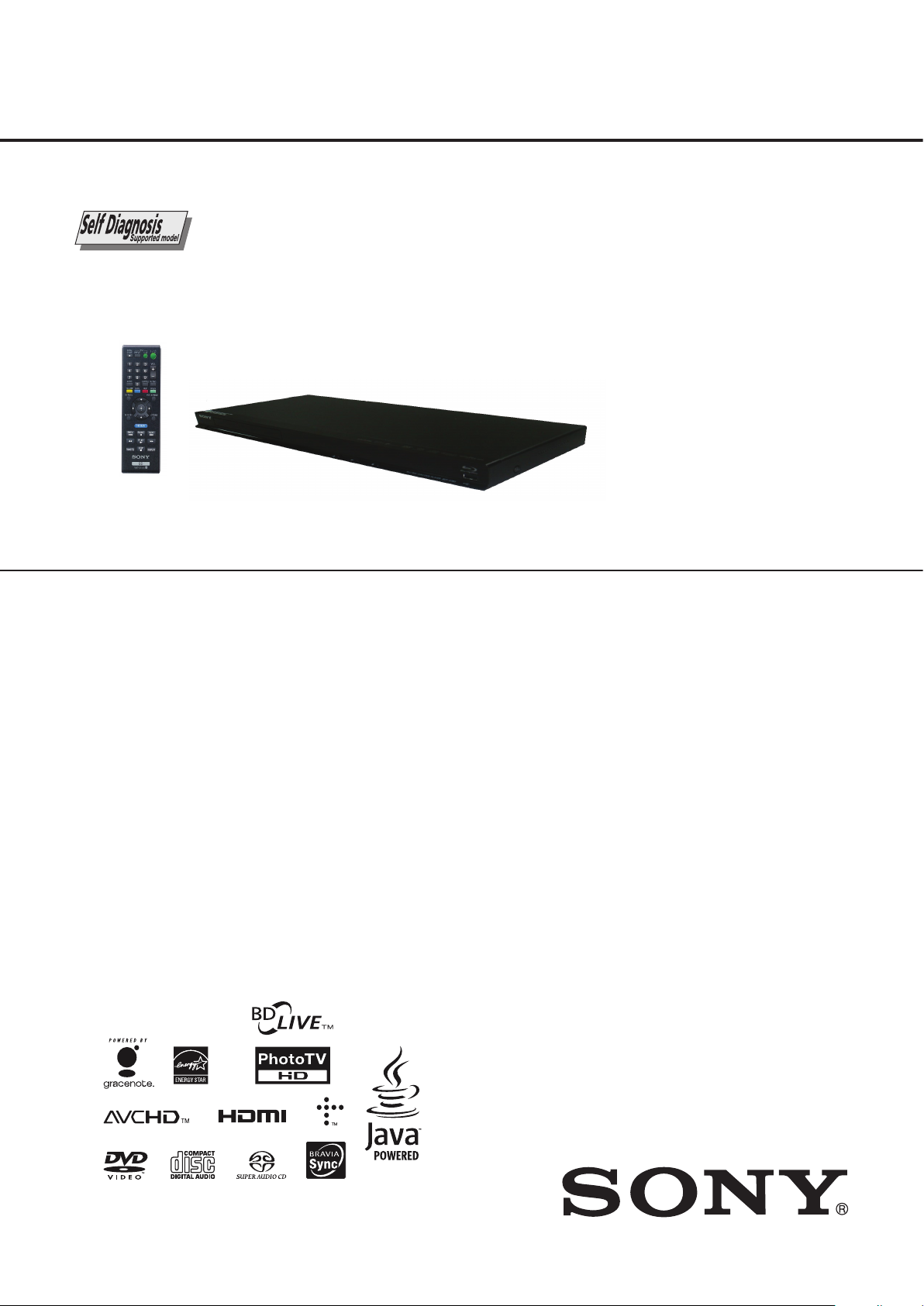
BDP-BX38/S280/S380/S383
RMT-B109A/B109P/B109C/B110A/B110P
SERVICE MANUAL
Canadian Model
Ver. 1.0 2010.12
BDP-S280/S380/BX38
Brazilian Model
Photo: BDP-S280
Remote : RMT-B109A
SPECIFICATIONS
AEP Model
UK Model
UK Model
BDP-S280/S380/S383
BDP-S280/S380/S383
US Model
BDP-S280
Argentina Model
E Model
Chinese Model
Indian Model
Middle East Model
Russian Model
Saudi Arabia Model
Singapore Model
Taiwan Model
Thailand Model
Australian /
New Zealand Model
PX Model
BDP-S380
System
Laser: Semiconductor laser
Inputs and outputs
(Jack name:
Jack type/Output level/Load impedance)
LINE OUT R-AUDIO-L::
Phone jack/2 Vrms/10 kilohms
DIGITAL OUT (COAXIAL):
Phono jack/0.5 Vp-p/75 ohms
HDMI OUT:
HDMI 19-pin standard connector
COMPONENT VIDEO OUT
(Y, P
B, P R
) :
Phono jack/Y: 1.0 Vp-p/
P
B , PR : 0.7 Vp-p/75 ohms
LINE OUT VIDEO:
Phono jack/1.0 Vp-p/75 ohms
LAN (100):
100BASE-TX Terminal
USB:
USB jack Type A (For connecting a USB memory,
memory card reader,digital stil camera and digital
video camera)
All model (REAR USB)
BDP-BX38/S380/S383 (FRONT USB)
General
Power requirements:
120V AC, 60
220 – 240V AC, 50/60Hz (AEP,UK, AUS,RUS,CN)
110 – 240V AC, 50/60Hz (PX,E,AR,BR,SP,TH,EA,KS,IN)
110V AC, 60Hz (TW)
Power consumption:
18 W (BDP-S380/S383/BX38)
16 W (BDP-S280)
Dimensions (approx.):
430 mm × 199 mm × 36mm
7 in. × 7
(1
(width/depth/height) incl. projecting parts
Mass (approx.):
Operating temperature:
5 ºC to 35 ºC(41 F to 95 F)
Operating humidity:
25 % to 80 %
Supplied accessories
• Audio/video cable (phono plug ×3) (1)
(Except AEP,UK,E,AR,SP,TH,CN,IN,TW)
LAN cable
• (1) (BDP-S380 : TW only)
• HDMI cable (1) (Except AEP,UK,AUS,US,CND,PX,RUS)
• Remote commander (remote) (1)
• Size AA (R6) batteries (2)
Specifications and design are subject to change
without notice.
ENERGY STAR and the ENERGY STAR mark
are registered U.S. marks. ENERGY STAR is a
registered mark owned by the U.S. government.
(BDP-S280:US/S380:US/BX38:US)
gk6..1
Hz (US, CND)
4
/5 in. ×
º
1
7
/16 in.)
º
TM
9-890-744-11
BLU-RAY
Sony Corporation
Home Entertainment Business Group
DISC / DVD PLAYER
2010L 6900-1
© 2010.12
Published by Design Engineering Dept.
Page 2
BDP-BX38/S280/S380/S383
1.5k
Ω
0.15µF
(0.75 V)
Parts on Set
Earth Ground
WARNING
To reduce the risk of re or electric
shock, do not expose this apparatus
to rain or moisture.
To avoid electrical shock, do not
open the cabinet. Refer servicing to
quali
ed personnel only.
Batteries or batteries installed
apparatus shall not be exposed to
excessive heat such as sunshine,
re or the like.
CAUTION
The use of optical instruments with
this product will increase eye
hazard. As the laser beam used in
this Blu-ray Disc/DVD player is
harmful to eyes, do not attempt to
disassemble the cabinet.
Refer servicing to quali
ed
personnel only.
Notice for customers in the
United Kingdom and
Republic of Ireland
A molded plug complying with
BS1363 is
tted to this equipment
for your safety and convenience.
Should the fuse in the plug
supplied need to be replaced, a 5
AMP fuse approved by ASTA or
BSI to BS1362, (i.e., marked with
or mark) must be used.
If the plug supplied with this
equipment has a detachable fuse
cover, be sure to attach the fuse
cover after you change the fuse.
Never use the plug without the fuse
cover. If you should lose the fuse
cover, please contact your nearest
Sony service station.
Disposal of Old Electrical
& Electronic Equipment
(Applicable in the
European Union and
other European countries
with separate collection
systems)
This symbol on the product or on
its packaging indicates that this
product shall not be treated as
household waste. Instead it shall be
Disposal of was
batteries (appli
the European Un
other Europea
with separate
systems)
This symbol on the
the packaging in
battery provided
shall not be trea
waste.
By ensuring thes
disposed of correctl
prevent potentia
consequences fo
and human heal
otherwise be cau
inappropriate wa
battery. The recyc
materials will he
natural resource
In case of product
performance or
reasons require
connection with
battery,
this batte
replaced by qua
only.
SAFETY CHECK-OUT
After correcting the original service problem, perform the following
safety checks before releasing the set to the customer:
1. Check
of your repair for unsoldered or poorly-soldered
the
area
connections. Check the entire board surface for solder splashes
and bridges.
2. Check the interboard wiring to ensure that no wires are “pinched”
or contact high-wattage resistors.
3. Look for unauthorized replacement parts, particularly transistors,
that were installed during a previous repair. Point them out to
the customer and recommend their replacement.
4. Look for parts which, though functioning, show obvious signs
of deterioration. Point them out to the customer and recommend
their replacement.
5. Check the line cord for cracks and abrasion. Recommend the
replacement of any such line cord to the customer.
6. Check the B+ voltage to see it is at the values specified.
7. Check
the antenna terminals, metal trim, “metallized” knobs,
screws, and all other exposed metal parts for AC leakage. Check
leakage as described below.
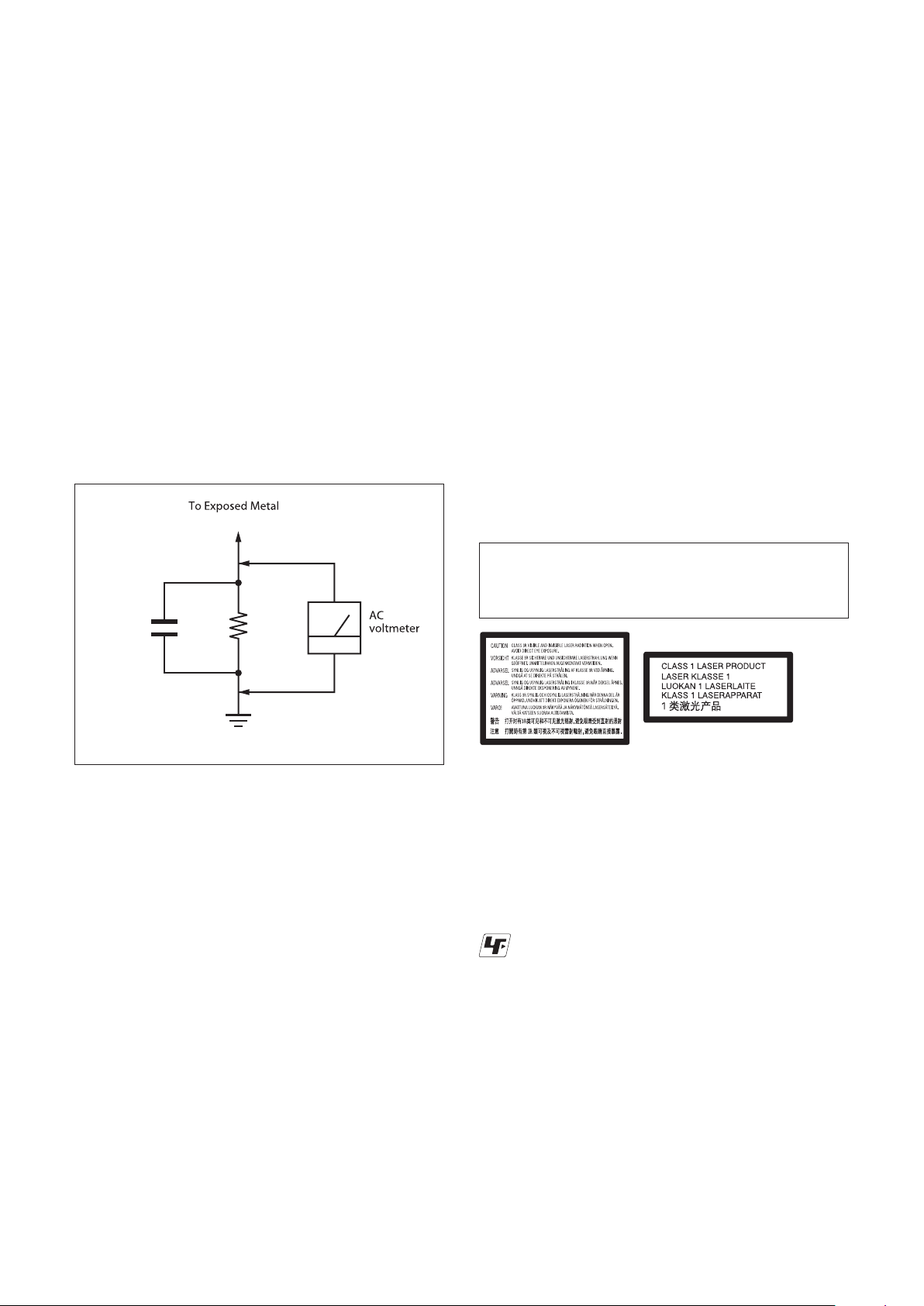
LEAKAGE TEST
The AC leakage from any exposed metal part to earth ground and
from all exposed metal parts to any exposed metal part having a
return to chassis, must not exceed 0.5 mA (500 microamperes).
Leakage current can be measured by any one of three methods.
1. A commercial leakage tester, such as the Simpson 229 or RCA
WT-540A. Follow the manufacturers' instructions to use these
instruments.
2. A battery-operated AC milliammeter. The Data Precision 245
digital multimeter is suitable for this job.
3. Measuring the voltage drop across a resistor by means of a
VOM or battery-operated AC voltmeter. The “limit” indication
is 0.75V, so analog meters must have an accurate low-voltage
scale. The Simpson 250 and Sanwa SH-63Trd are examples of a
passive VOM that is suitable. Nearly all battery operated digital
multimeters that have
a 2V AC range are suitable. (See Fig. A)
CAUTION:
The use of optical instrument with this product will increase eye
hazard.
CAUTION
Use of controls or adjustments or performance of procedures
other than those specified herein may result in hazardous radiation exposure.
Fig. A. Using an AC voltmeter to check AC leakage.
WHEN SERVICING, DO NOT APPROACH THE LASER
EXIT WITH THE EYE TOO CLOSELY. IN CASE IT IS
NECESSARY TO CONFIRM LASER BEAM EMISSION,
THAN 25 cm FROM THE SURFACE OF THE OBJECTIVE LENS ON THE OPTICAL PICK-UP BLOCK.
SAFETY-RELATED COMPONENT WARNING!!
COMPONENTS IDENTIFIED BY MARK 0 ENIL DETTOD RO
WITH MARK 0 NI DNA SMARGAID CITAMEHCS EHT NO
THE PARTS LIST ARE CRITICAL TO SAFE OPERATION. RE-
IN SUPPLEMENTS PUBLISHED BY SONY.
ATTENTION AU COMPOSANT AYANT RAPPORT
OMPOSANTS IDENTIFIÉS PAR UNE MARQUE 0
LES C
DONNÉS DANS CE MANUEL OU DANS LES SUPPLÉMENTS PUBLIÉS PAR SONY.
WARNING!!
À LA SÉCURITÉ!
For customers in European countries
This appliance is classied as a CLASS 1 LASER
This label is located on the laser
protective housing inside the
enclosure.
product. The CLASS 1 LASER PRODUCT
MARKING is located on the rear exterior.
Unleaded solder
Boards requiring use of unleaded solder are printed with the leadfree mark (LF) indicating the solder contains no lead.
EROM FO ECNATSID A MORF EVRESBO OT ERUS EB
(Caution: Some printed circuit boards may not come printed with
the lead free mark due to their particular size.)
: LEAD FREE MARK
Unleaded solder has the following characteristics.
• Unleaded solder melts at a temperature about 40°C higher than
ordinary solder.
Ordinary soldering irons can be used but the iron tip has to be
ESOHW STRAP YNOS HTIW STNENOPMOC ESEHT ECALP
RO LAUNAM SIHT NI NWOHS SA RAEPPA SREBMUN TRAP
applied to the solder joint for a slightly longer time.
Soldering irons using a temperature regulator should be set to
about 350°C.
Caution: The printed pattern (copper foil) may peel away if the
heated tip is applied for too long, so be careful!
• Strong viscosity
Unleaded solder is more viscous (sticky, less prone to flow) than
ETSIL AL TE SEUQITAMÉHCS SEMMARGAID SEL RUS
ED ÉTIRUCÉS AL RUOP SEUQITIRC TNOS SECÈIP SED
STNASOPMOC SEC RECALPMER EN .TNEMENNOITCNOF
TNOS SORÉMUN SEL TNOD YNOS SECÈIP SED RAP EUQ
ordinary solder so use caution not to let solder bridges occur such
as on IC pins, etc.
• Usable with ordinary solder
It is best to use only unleaded solder but unleaded solder may
also be added to ordinary solder.
– 2 –
Page 3

1. SERVICE NOTE
BDP-BX38/S280/S380/S383
TABLE OF CONTENTS
egaP eltiT noitceS egaP eltiT noitceS
1-1. Disc Removal Procedure If The Tray Cannot Be
Ejected (Forced Ejection) ............................................. 1-1
1-2. Work when optical device are replaced ........................ 1-1
1-3. Test Disc ....................................................................... 1-2
1-3-1. Operation and Display ............................................. 1-2
1-3-2. Main functions ......................................................... 1-9
1-4. Drive Repairing............................................................. 1-15
1-4-1. Preparation .............................................................. 1-15
1-4-2. Checking Flow ~ Drive (BU) section ~ .................... 1-15
1-4-3. BU Check Flow [zz] ~ .............................................. 1-16
1-4-4. BU (Optical Block) Repair Guide ............................. 1-16
1-4-5. BU Adjustment Flow [yy] ~ ...................................... 1-17
1-4-6. KEM-470AAA/C2RP Packing Spec. ....................... 1-17
1-4-7. KEM-470AAA/C2RP Packing .................................. 1-18
1-4-8. BU Data Decode Jig ................................................ 1-19
1-4-9.
1-4-10. Laser Caution Label ................................................ 1-20
Loading For Service
1-5. Rear Panel Assembly Caution...................................
.........................................
1-20
1-23E
2. DISASSEMBLY
2-1. Disassembly Flow ........................................................ 2-1
2-2. Upper Case .................................................................. 2-1
2-3. Tray Cover Assy .......................................................... 2-2
2-4. Front Panel Assy, FL-203 and IF-170 Board .... ............... 2-2
2-5. Rear Panel Block ......................................................... 2-3
2-6. MB-138 Board ............................................................. 2-3
2-7. BD Drive
2-8. Switching Regulator ..................................................... 2-5E
2-9. Circuit Boards Location ................................................ 2-5E
.....................................................................
.. 2-4
4-12. MB-138 Board (HDMI)
Schematic Diagram (7/14)............................................ 4-12
4-13. MB-138 Board (ETHERNET)
Schematic Diagram (8/14)............................................ 4-13
4-14. MB-138 Board (AUDIO)
Schematic Diagram (9/14)............................................ 4-14
4-15. MB-138 Board (VIDEO)
Schematic Diagram (10/14).......................................... 4-15
4-16. MB-138 Board (GPIO/JTAG)
Schematic Diagram (11/14) .......................................... 4-16
4-17. MB-138 Board (IF CON)
Schematic Diagram (12/14).......................................... 4-17
4-18. MB-138 Board (FE_POWER/OP/GIO)
Schematic Diagram (13/14).......................................... 4-18
4-19. MB-138 Board (FE_POWER/MOTOR DRIVE)
Schematic Diagram (14/14) ........................................ 4-19
4-20. Waveforms ................................................................... 4-20E
5. PRINTED WIRING BOARDS
5-1. This Note Is Common For Printed Wiring Boards ........ 5-1
5-2. FL-203 Board (FRONT LEFT) Printed Wiring Board..... 5-2
5-3. IF-170 Board
Printed Wiring Board ...................................................... 5-3
5-4. MB-138 Board(MAIN)
Printed Wiring Board (Side A) ..................................... 5-4
5-5. MB-138 Board (MAIN)
Printed Wiring Board (Side B) ...................................... 5-5E
3. BLOCK DIAGRAMS
3-1. Overall Block Diagram.................................................. 3-1
3-2. DSP Block Diagram ...................................................... 3-2
3-3. AV OUT Block Diagram ................................................ 3-3
3-4. USB/ETHER, Block Diagram .................................. 3-4
3-5. Power Block Diagram .......................................... 3-5E
4. SCHEMATIC DIAGRAMS
4-1. This Note Is Common For Schematic Diagrams .......... 4-1
4-2. Frame Schematic Diagram........................................... 4-2
4-3. IF-170 Board (FRONT LEFT) Schematic Diagram ... 4-3
IF-170 Board (USB FRONT) Schematic Diagram ......
4-4.
4-5. FL-203 Board (FRONT RIGHT)
4-6. MB-138 Board (DDR 3 A)
Schematic Diagram (1/14)............................................ 4-6
4-7. MB-138 Board (DDR 3 B)
Schematic Diagram (2/14)............................................ 4-7
4-8. MB-138 Board (POWER)
Schematic Diagram (3/14)............................................ 4-8
4-9. MB-138 Board (CLK/POWER)
Schematic Diagram (4/14)............................................ 4-9
4-10. MB-138 Board (FLASH/HOST)
Schematic Diagram (5/14)............................................ 4-10
4-11. MB-138 Board (USB) Schematic Diagram (6/14)......... 4-11
Schematic Diagram ... 4-5
4-4
6. IC PIN FUNCTION DESCRIPTION ................... 6-1
7. SERVICE MODE ..................................................... 7-1
8. ERROR LOG LIST ................................................. 8-1
9. TROUBLESHOOTING ............................................. 9-1
10. REPAIR PARTS LIST
10-1. Exploded Views ............................................................ 10-1
10-1-1. Case Section ........................................................... 10-1
10-1-2. ........................................... 10-2
10-1-3.
10-1-4.
10-2. Electrical Parts List ....................................................... 10-5
Main Chassis Section
BD Section
Accessories
.............................................................
.......................................................... 10-4
10-3
– 3 –
Page 4
BDP-BX38/S280/S380/S383
SECTION 1
SERVICE NOTE
1-1. DISC REMOVAL PROCEDURE IF THE TRAY CANNOT BE EJECTED (FORCED EJECTION)
1. Remove the upper case. (Refer to page 2-1)
2. Insert a clip in the hole of a drive and open a tray.
Note:
(Use clip diameter about 1.2 mm)
(12~32)mm
clip
hole
Fig.1
tray
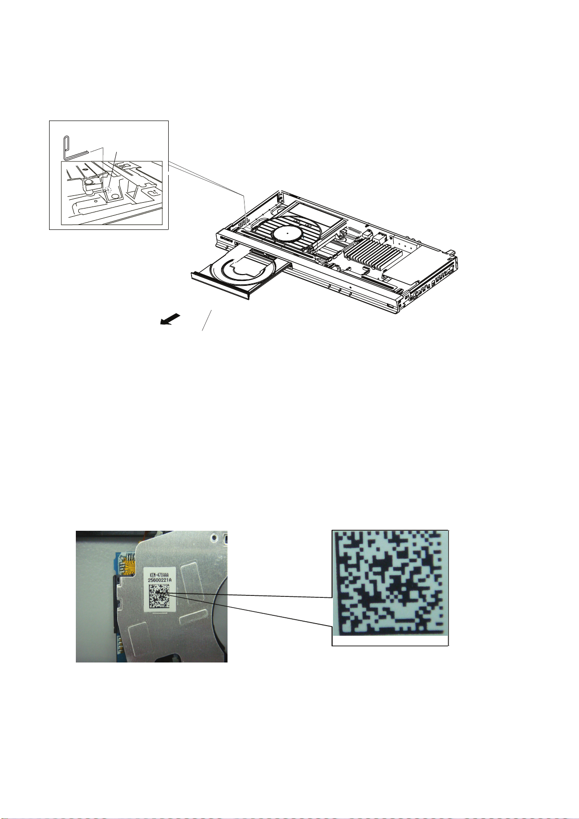
1-2. Work when optical device are replaced
Note: Please do the following work when you replace the optical device.
1. Install it in PC after downloading two set of software from following URL.
(Refer to “1-4-9. BU Data Decode Jig” on page 1-19)
STEP 1
Microsoft .NET Framework Version 2.0 Redistributable Package (x86)
http://www.microsoft.com/downloads/details.aspx?displaylang=en&FamilyID=0856eacb-4362-4b0d-8edd-aab15c5e04f5
STEP 2
Microsoft .NET Framework 2.0 Service Pack 1 (x86)
http://www.microsoft.com/downloads/details.aspx?displaylang=en&FamilyID=79bc3b77-e02c-4ad3-aacf-a7633f706ba5
2. Take a photograph of the bar code on the optical device. The valid bar code photo as shown in Fig.2
Fig.2
3. Drag-and-drop the bar code photograph to the icon of decode software (BDPRdec).
* The decode software is a complete set of “BDPRdec”, “Tasman.Bars.dll”, and “SavePath”.
* Because decode software cannot be attached, it separately distributes it.
4. Input the password when you start decode software.
* Inquire of each service headquarters because the password cannot be disclosed.
5. Write the decode data to the set.
(Refer to “1-4-4. BU (Optical Block) Repair Guide” on page 1-16 and “1-4-5. BU Adjustment Flow [yy]” on page 1-17)
1-1
Page 5

BDP-BX38/S280/S380/S383
1-3. TEST DISC
Part No. Description Layer
J-6090-199-A BLX-104 Single Layer
J-6090-200-A BLX-204 Dual Layer
J-2501-307-A CD (HLX-A1)
J-2501-305-A HLX-513 Single Layer (NTSC)
J-2501-306-A HLX-514 Dual Layer (NTSC)
J-6090-077-A HLX-506 Single Layer (PAL)
J-6090-078-A HLX-507 Dual Layer (PAL)
1-3-1. Operation and Display
Check Items
1) BLX-104
1. Select 23.976Hz/1080p
2. Play “4.Motion pictures”
3. Check whether player can play back or not
4. Check each outputs
Video:
Composite/component/HDMI
Audio:
Digital out (Coaxial/Optical)/Audio out/5.1Ch output
* When 1080/24p monitor is nothing, 1080i (59.94Hz or 50Hz) can use instead of 1080/24p.
However this is temporary correspondence.
2) BLX-204
1. Select 1080i (59.94Hz or 50Hz)
2. Play “4.Motion pictures”
3. Check whether player can play back or not
(Check the picture and sound output)
3) CD (HLX-A1)
Check whether player can play back or not
(Check the sound output)
4) HLX-513/514 (NTSC), HLX-506/507 (PAL)
1. After displayed Main Menu, select “1.Video”
2. Play “1.Color Bar 100%”
(Check the picture and sound output)
3. Return to Menu
4. Play “Demonstration 4:3” or “5.Demonstration 16:9”
(Check the picture and sound output)
1-2
Page 6
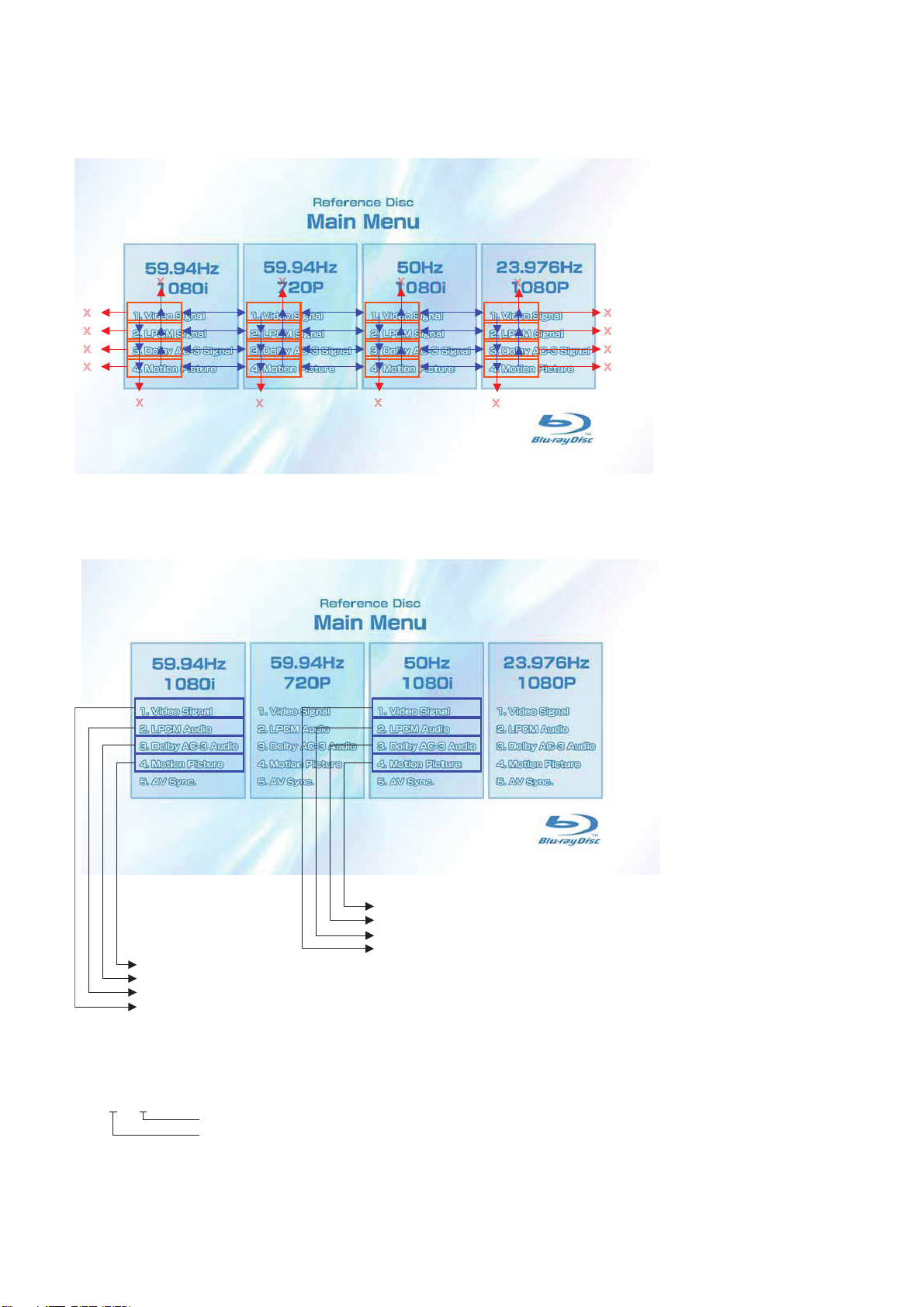
1-3-1-1. BLX-104 Menu Function (1)
Main Menu
BDP-BX38/S280/S380/S383
X X X
X
X
X
X
X
X
X
X
X
X
X
X
X
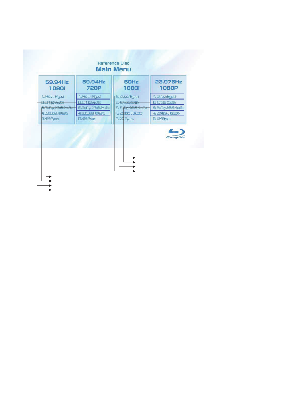
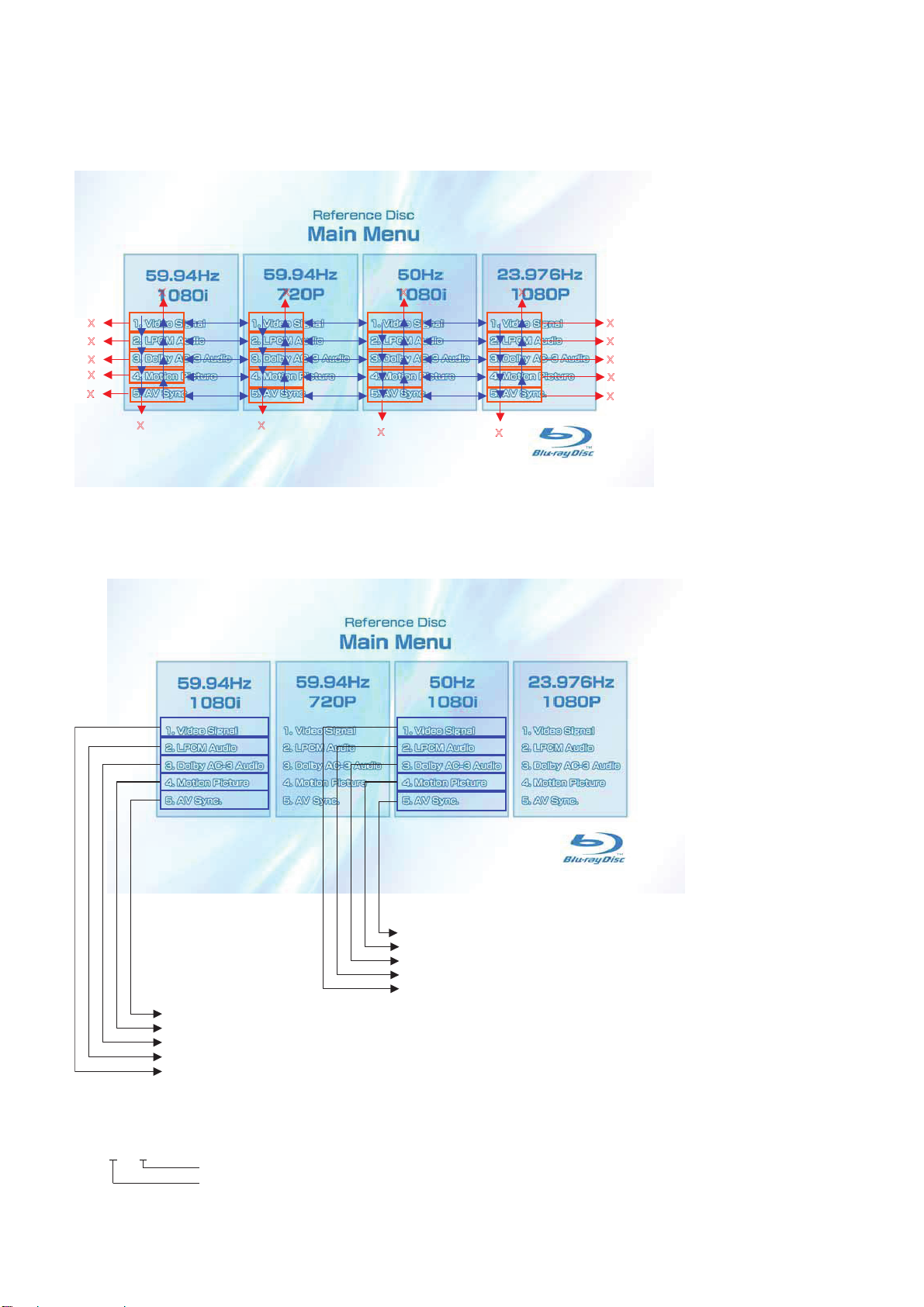
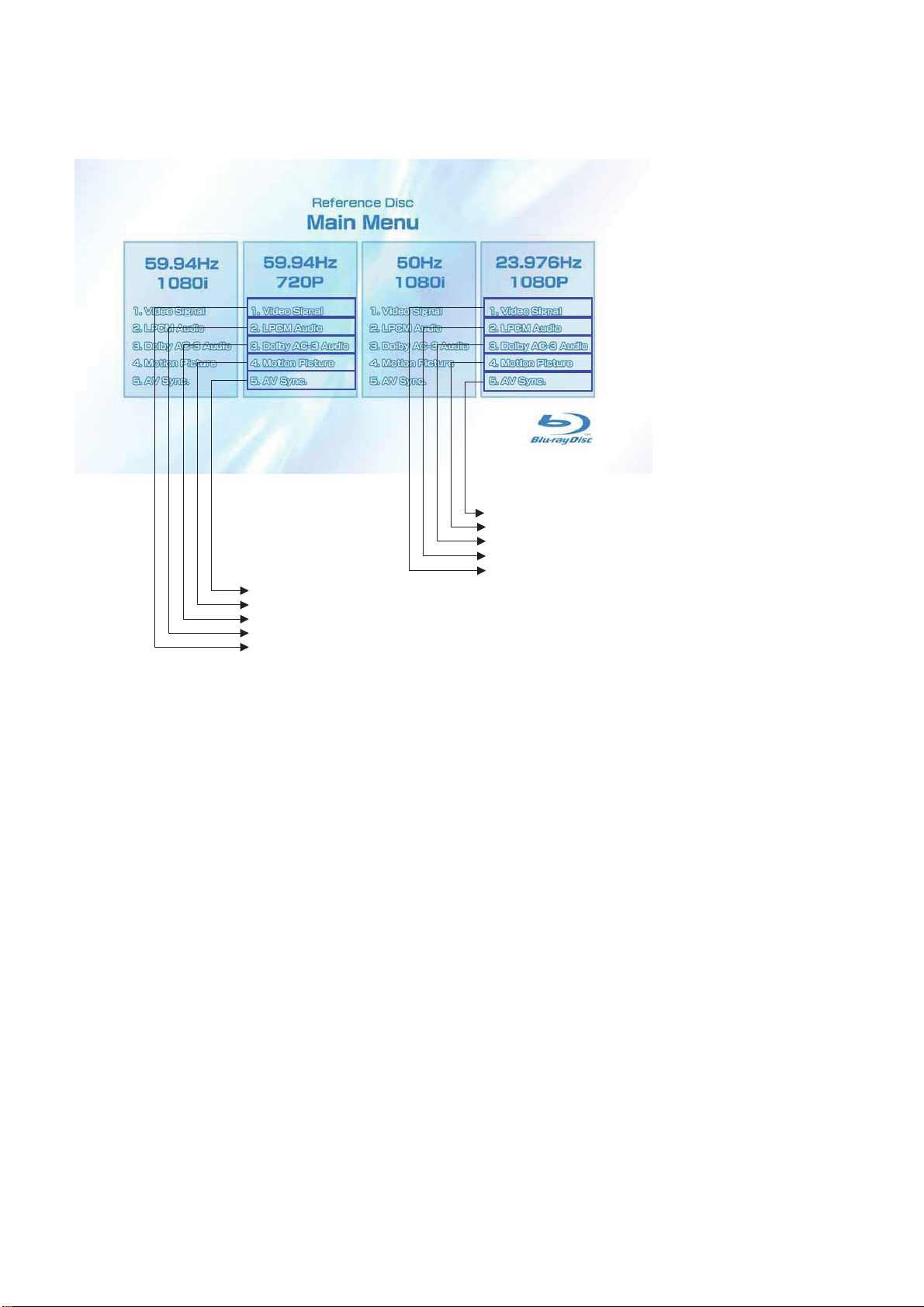
1) When the disc is inserted, 1. Video Signal of 59.94Hz/1080i of the Main Menu is selectively displayed.
1-3-1-2. BLX-104 Menu Function (2)
Main Menu
To Main Menu after playback of T62_C1
To Main Menu after playback of T61_C1
To Main Menu after playback from T54_C1 to T60_C1
Sub_menu3 is displayed
To Main Menu after playback of T21_C1
To Main Menu after playback of T20_C1
To Main Menu after playback from T2_C1 to T19_C1
Sub_menu1 is displayed
* When returning to Main Menu after playback from each button of 59.94Hz/1080i, 1. Video Signal of 59.94Hz/1080i is selectively dis-
played.
* When returning to Main Menu after playback from each button of 50Hz/1080i, 1. Video Signal of 50Hz/1080i is selectively displayed.
* 5. AV Sync does not operate.
Note:
Txx_ Cxx
Chapter No.
Title No.
1-3
Page 7
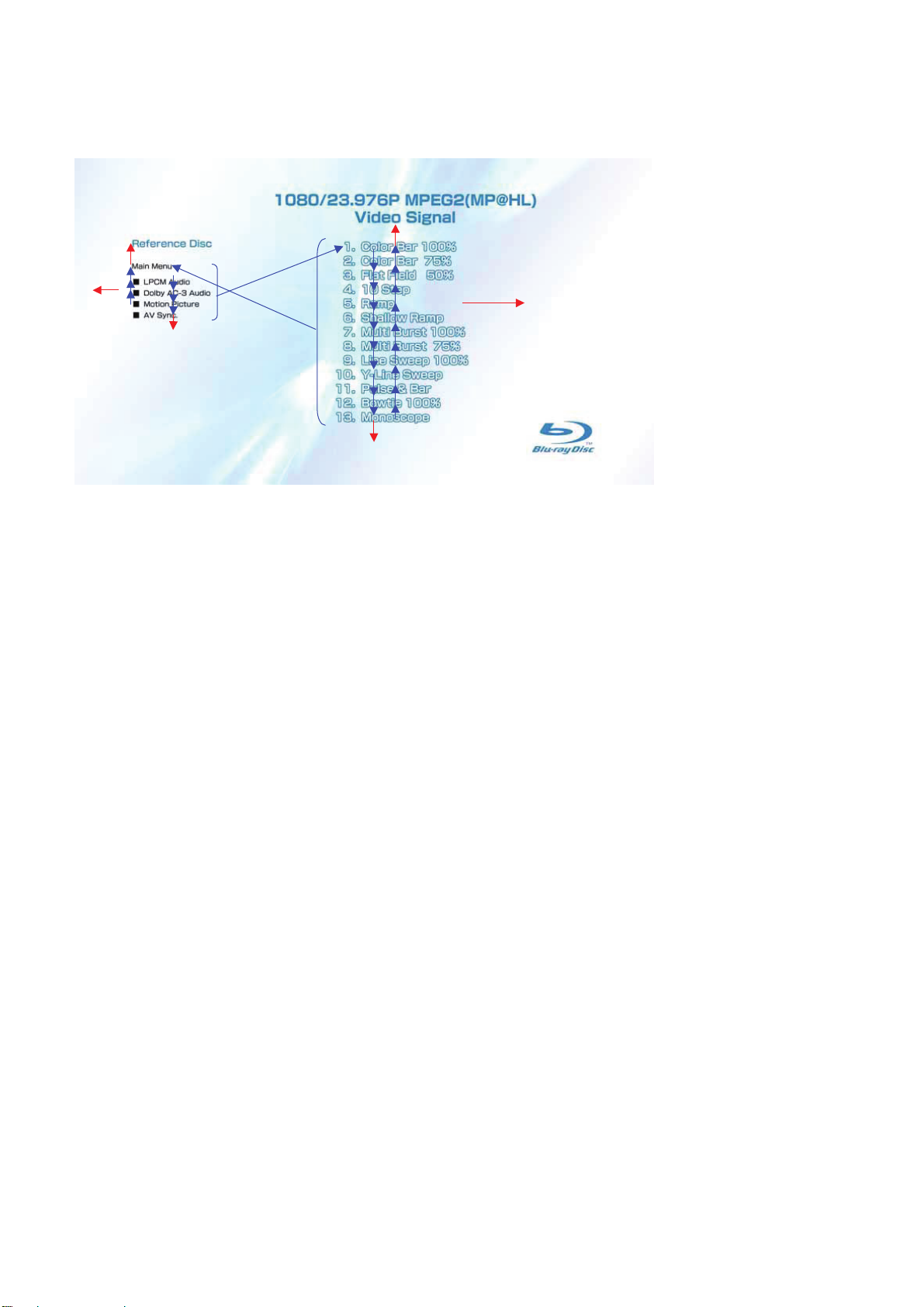
1-3-1-3. BLX-104 Menu Function (3)
Main Menu
BDP-BX38/S280/S380/S383
To Main Menu after playback of T52_C1
To Main Menu after playback of T51_C1
To Main Menu after playback from T44_C1 to T50_C1
Sub_menu2 is displayed
To Main Menu after playback of T42_C1
To Main Menu after playback of T41_C1
To Main Menu after playback from T23_C1 to T40_C1
Sub_menu4 is displayed
* When returning to Main Menu after playback from each button of 59.94Hz/720P, 1. Video Signal of 59.94Hz/720P is selectively dis-
played.
* When returning to Main Menu after playback from each button of 23.976Hz/1080P, 1. Video Signal of 23.976Hz/1080P is selectively
displayed.
* 5. AV Sync does not operate.
1-4
Page 8

1-3-1-4. BLX-104 Menu Function (4)
Sub menu1
X
BDP-BX38/S280/S380/S383
X
X
X
X
X
1) At the display of Sub menu1, 1. Color Bar 100% is selectively displayed.
2) Selection of 1. Color Bar 100% t Return to Sub menu1 after seamless playback from T1_C1 to T1_C13. 1. Color Bar 100% is selec-
tively displayed on Sub menu1 screen.
3) Selection of 2. Color Bar 75% t Return to Sub menu1 after seamless playback from T1_C2 to T1_C13. 1. Color Bar 100% is selectively
displayed on Sub menu1 screen.
4) At the selection of 3 - 13, item 3 mentioned above is executed as the routine.
5) At the display of Sub menu1, Main Menu is selected t Jump to Main Menu. At the display of Main Menu, 1. Video Signal of 59.94Hz/1080i
is selectively displayed.
6) Selection of LPCM Audio t Playback from T2_C1 to T19_C1. SubPic that corresponds to Audio stream 1 is forcibly displayed.
During the playback, when audio channel changes, the caption that corresponds to each audio stream is forcibly displayed. Return to
Sub menu1 after playback. 1. Color Bar 100% is selectively displayed on Sub menu1 screen.
7) Selection of Dolby AC-3 Audio t Playback of T20_C1. SubPic that corresponds to Audio stream 1 is forcibly displayed.
During the playback, when audio channel changes, the caption that corresponds to each audio stream is forcibly displayed. Return to
Sub menu1 after playback. 1. Color Bar 100% is selectively displayed on Sub menu1 screen.
8) Selection of
Motion Picture t Return to Sub menu1 after playback of T21_C1. 1. ColorBar 100% is selectively displayed on Sub
menu1 screen.
9) At the selection of Main Menu, 1. VideoSignal of 1080/59.94i of Main Menu is selectively displayed.
10) AV Sync does not operate.
1-5
Page 9
1-3-1-5. BLX-104 Menu Function (5)
Sub menu2
X
BDP-BX38/S280/S380/S383
X
X
X
X
X
1) At the display of Sub menu2, 1. Color Bar 100% is selectively displayed.
2) Selection of 1. Color Bar 100% t Return to Sub menu2 after seamless playback from T43_C1 to T43_C13. 1. Color Bar 100% is
selectively displayed on Sub menu2 screen.
3) Selection of 2. Color Bar 75% t Return to Sub menu2 after seamless playback from T43_C2 to T43_C13. 1. Color Bar 100% is se-
lectively displayed on Sub menu2 screen.
4) At the selection of 3 - 13, item 3 mentioned above is executed as the routine.
5) At the display of Sub menu2, Main Menu is selected t Jump to Main Menu. At the display of Main Menu, 1. Video Signal of
23.976Hz/1080P is selectively displayed.
6) Selection of LPCM Audio t Playback from T44_C1 to T50_C1. SubPic that corresponds to Audio stream 1 is forcibly displayed.
During the playback, when audio channel changes, the caption that corresponds to each audio stream is forcibly displayed. Return to
Sub menu2 after playback. 1. Color Bar 100% is selectively displayed on Sub menu2 screen.
7) Selection of Dolby AC-3 Audio t Playback of T51_C1. SubPic that corresponds to Audio stream 1 is forcibly displayed.
During the playback, when audio channel changes, the caption that corresponds to each audio stream is forcibly displayed. Return to
Sub menu2 after playback. 1. Color Bar 100% is selectively displayed on Sub menu2 screen.
8) Selection of Motion Picture t Return to Sub menu2 after playback of T52_C1. 1. Color Bar 100% is selectively displayed on Sub
menu2 screen.
9) At the selection of Main Menu, 1. Video Signal of 1080/23.976P of Main Menu is selectively displayed.
10) AV Sync does not operate.
1-6
Page 10

1-3-1-6. BLX-104 Menu Function (6)
Sub menu3
X
BDP-BX38/S280/S380/S383
X
X
X
X
X
1) At the display of Sub menu3, 1. Color Bar 100% is selectively displayed.
2) Selection of 1. Color Bar 100% t Return to Sub menu3 after seamless playback from T53_C1 to T53_C13. 1. Color Bar 100% is
selectively displayed on Sub menu3 screen.
3) Selection of 2. Color Bar 75% t Return to Sub menu3 after seamless playback from T53_C2 to T53_C13. 1. Color Bar 100% is se-
lectively displayed on Sub menu3 screen.
4) At the selection of 3 - 13, item 3 mentioned above is executed as the routine.
5) At the display of Sub menu3, Main Menu is selected t Jump to Main Menu. At the display of Main Menu, 1. Video Signal of 50Hz/1080i
is selectively displayed.
6) Selection of LPCM Audio t Playback from T54_C1 to T60_C1. SubPic that corresponds to Audio stream 1 is forcibly displayed.
During the playback, when audio channel changes, the caption that corresponds to each audio stream is forcibly displayed. Return to
Sub menu3 after playback. 1. Color Bar 100% is selectively displayed on Sub menu3 screen.
7) Selection of Dolby AC-3 Audio t Playback of T61_C1. SubPic that corresponds to Audio stream 1 is forcibly displayed.
During the playback, when audio channel changes, the caption that corresponds to each audio stream is forcibly displayed. Return to
Sub menu3 after playback. 1. Color Bar 100% is selectively displayed on Sub menu3 screen.
8) Selection of Motion Picture t Return to Sub menu3 after playback of T62_C1. 1. Color Bar 100% is selectively displayed on Sub
menu3 screen.
9) At the selection of Main Menu, 1. Video Signal of 1080/50i of Main Menu is selectively displayed.
10) AV Sync does not operate.
1-7
Page 11

1-3-1-7. BLX-104 Menu Function (7)
Sub menu4
X
BDP-BX38/S280/S380/S383
X
X
X
X
X
1) At the display of Sub menu4, 1. Color Bar 100% is selectively displayed.
2) Selection of 1. Color Bar 100% t Return to Sub menu4 after seamless playback from T22_C1 to T22_C13. 1. Color Bar 100% is
selectively displayed on Sub menu4 screen.
3) Selection of 2. Color Bar 75% t Return to Sub menu4 after seamless playback from T22_C2 to T22_C13. 1. Color Bar 100% is se-
lectively displayed on Sub menu4 screen.
4) At the selection of 3 - 13, item 3 mentioned above is executed as the routine.
5) At the display of Sub menu4, Main Menu is selected t Jump to Main Menu. At the display of Main Menu, 1. Video Signal of 59.94Hz/720P
is selectively displayed.
6) Selection of LPCM Audio t Playback from T44_C1 to T50_C1. SubPic that corresponds to Audio stream 1 is forcibly displayed.
During the playback, when audio channel changes, the caption that corresponds to each audio stream is forcibly displayed. Return to
Sub menu4 after playback. 1. Color Bar 100% is selectively displayed on Sub menu4 screen.
7) Selection of Dolby AC-3 Audio t Playback of T51_C1. SubPic that corresponds to Audio stream 1 is forcibly displayed.
During the playback, when audio channel changes, the caption that corresponds to each audio stream is forcibly displayed. Return to
Sub menu4 after playback. 1. Color Bar 100% is selectively displayed on Sub menu4 screen.
8) Selection of Motion Picture t Return to Sub menu4 after playback of T52_C1. 1. Color Bar 100% is selectively displayed on Sub
menu4 screen.
9) At the selection of Main Menu, 1. Video Signal of 720/59.94P of Main Menu is selectively displayed.
V Sync does not operate.
10) A
1-8
Page 12
BDP-BX38/S280/S380/S383
1-3-2
Menu Function
1-3-2-1. BLX-204 Menu Function (1)
Main Menu
X X X X
X
X
X
X
X
X
X
X
X
X
X
X
X
X
1) When the disc is inserted, 1. Video Signal of 59.94Hz/1080i of the Main Menu is selectively displayed.
1-3-2-2. BLX-204 Menu Function (2)
Main Menu
To Main Menu after playback of T83_C1
To Main Menu after playback of T62tT82
To Main Menu after playback of T61_C1
To Main Menu after playback of T54_C1-T60_C1tT83_C1-T94_C1
Sub_menu3 is displayed
To Main Menu after playback of T67_C1
To Main Menu after playback of T21tT63tT64tT65tT66
To Main Menu after playback of T20_C1
To Main Menu after playback from T2_C1 to T19_C1
Sub_menu1 is displayed
* When returning to Main Menu after playback from each button of 59.94Hz/1080i, 1. Video Signal of 59.94Hz/1080i is selectively dis-
played.
* When returning to Main Menu after playback from each button of 50Hz/1080i, 1. Video Signal of 50Hz/1080i is selectively displayed.
Note:
Txx_ Cxx
Chapter No.
Title No.
1-9
Page 13
1-3-2-3. BLX-204 Menu Function (3)
Main Menu
BDP-BX38/S280/S380/S383
To Main Menu after playback of T70_C1
To Main Menu after playback of T52_C1t T69
To Main Menu after playback of T51_C1
To Main Menu after playback of T44_C1-T50_C1t T71_C1-T81_C1
Sub_menu2 is displayed
To Main Menu after playback of T68_C1
To Main Menu after playback of T42_C1
To Main Menu after playback of T41_C1
To Main Menu after playback from T23_C1 to T40_C1
Sub_menu4 is displayed
* When returning to Main Menu after playback from each button of 59.94Hz/720P, 1. Video Signal of 59.94Hz/720P is selectively dis-
played.
* When returning to Main Menu after playback from each button of 23.976Hz/1080P, 1. Video Signal of 23.976Hz/1080P is selectively
displayed.
1-10
Page 14

1-3-2-4. BLX-204 Menu Function (4)
Sub menu 1
X
BDP-BX38/S280/S380/S383
X
X
X
X
X
1) At the display of Sub menu1, 1. Color Bar 100% is selectively displayed.
2) Selection of 1. Color Bar 100% t Return to Sub menu1 after seamless playback from T1_C1 to T1_C13. 1. Color Bar 100% is selec-
tively displayed on Sub menu1 screen.
3) Selection of 2. Color Bar 75% t Return to Sub menu1 after seamless playback from T1_C2 to T1_C13. 1. Color Bar 100% is selectively
displayed on Sub menu1 screen.
4) At the selection of 3 - 13, item 3 mentioned above is executed as the routine.
5) At the display of Sub menu1, Main Menu is selected t Jump to Main Menu. At the display of Main Menu, 1. Video Signal of
59.94Hz/1080i is selectively displayed.
6) Selection of LPCM Audio t Playback from T2_C1 to T19_C1. SubPic that corresponds to Audio stream 1 is forcibly displayed.
During the playback, when audio channel changes, the caption that corresponds to each audio stream is forcibly displayed. Return to
Sub menu1 after playback. 1. Color Bar 100% is selectively displayed on Sub menu1 screen.
7) Selection of Dolby AC-3 Audio t Playback of T20_C1. SubPic that corresponds to Audio stream 1 is forcibly displayed.
During the playback, when audio channel changes, the caption that corresponds to each audio stream is forcibly displayed. Return to
Sub menu1 after playback. 1. Color Bar 100% is selectively displayed on Sub menu1 screen.
8) Selection of Motion Picture t Return to Sub menu1 after playback of T21_C1. 1. Color Bar 100% is selectively displayed on Sub
menu1 screen.
9) Selection of AV Sync t Return to Sub menu1 after playback of T67_C1. 1. Color Bar 100% is selectively displayed on Sub menu1
screen.
10) At the selection of Main Menu, 1. Video Signal of 1080/59.94i of M
ain Menu is selectively displayed.
1-11
Page 15

1-3-2-5. BLX-204 Menu Function (5)
Sub menu 2
X
BDP-BX38/S280/S380/S3838
X
X
X
X
X
1) At the display of Sub menu2, 1. Color Bar 100% is selectively displayed.
2) Selection of 1. Color Bar 100% t Return to Sub menu2 after seamless playback from T43_C1 to T43_C13. 1. Color Bar 100% is
selectively displayed on Sub menu2 screen.
3) Selection of 2. Color Bar 75% t Return to Sub menu2 after seamless playback from T43_C2 to T43_C13. 1. Color Bar 100% is se-
lectively displayed on Sub menu2 screen.
4) At the selection of 3 - 13, item 3 mentioned above is executed as the routine.
5) At the display of Sub menu2, Main Menu is selected t Jump to Main Menu. At the display of Main Menu, 1. Video Signal of
23.976Hz/1080P is selectively displayed.
6) Selection of LPCM Audio t Playback from T44_C1 to T50_C1 and from T71_C1 to T81_C1. SubPic that corresponds to Audio stream
1 is forcibly displayed.
During the playback, when audio channel changes, the caption that corresponds to each audio stream is forcibly displayed. Return to
Sub menu2 after playback. 1. Color Bar 100% is selectively displayed on Sub menu2 screen.
7) Selection of Dolby AC-3 Audio t Playback of T51_C1. SubPic that corresponds to Audio stream 1 is forcibly displayed.
During the playback, when audio channel changes, the caption that corresponds to each audio stream is forcibly displayed. Return to
Sub menu2 after playback. 1. Color Bar 100% is selectively displayed on Sub menu2 screen.
8) Selection of Motion Picture t Return to Sub menu2 after playback of T52_C1 and T69. 1. Color Bar 100% is selectively displayed on
Sub menu2 screen.
9) Selection of AV Sync t
Return to Sub menu2 after playback of T70_C1. 1. Color Bar 100% is selectively displayed on Sub menu2
screen.
10) At the selection of Main Menu, 1. Video Signal of 1080/23.976P of Main Menu is selectively displayed.
1-12
Page 16

1-3-2-6. BLX-204 Menu Function (6)
Sub menu 3
X
BDP-BX38/S280/S380/S383
X
X
X
X
X
1) At the display of Sub menu3, 1. Color Bar 100% is selectively displayed.
2) Selection of 1. Color Bar 100% t Return to Sub menu3 after seamless playback from T53_C1 to T53_C13. 1. Color Bar 100% is
selectively displayed on Sub menu3 screen.
3) Selection of 2. Color Bar 75% t Return to Sub menu3 after seamless playback from T53_C2 to T53_C13. 1. Color Bar 100% is se-
lectively displayed on Sub menu3 screen.
4) At the selection of 3 - 13, item 3 mentioned above is executed as the routine.
5) At the display of Sub menu3, Main Menu is selected t Jump to Main Menu. At the display of Main Menu, 1. Video Signal of 50Hz/1080i
is selectively displayed.
6) Selection of LPCM Audio t Playback from T54_C1 to T60_C1 and from T84_C1 to T94_C1. SubPic that corresponds to Audio stream
1 is forcibly displayed.
During the playback, when audio channel changes, the caption that corresponds to each audio stream is forcibly displayed. Return to
Sub menu3 after playback. 1. Color Bar 100% is selectively displayed on Sub menu3 screen.
7) Selection of Dolby AC-3 Audio t Playback of T61_C1. SubPic that corresponds to Audio stream 1 is forcibly displayed.
During the playback, when audio channel changes, the caption that corresponds to each audio stream is forcibly displayed. Return to
Sub menu3 after playback. 1. Color Bar 100% is selectively displayed on Sub menu3 screen.
8) Selection of Motion Picture t Return to Sub menu3 after playback of T62_C1 and T82. 1. Color Bar 100% is selectively displayed on
Sub menu3 screen.
9) Selection of AV Sync t Return to Sub menu3 after playback of T83_C1. 1. Color Bar 100% is selectively displayed on Sub menu3
screen.
10) At the selection of Main Menu, 1. Video Signal of 1080/50i of Main Menu is selectively displayed.
1-13
Page 17

1-3-2-7. BLX-204 Menu Function (7)
Sub menu 4
X
BDP-BX38/S280/S380/S383
X
X
X
X
X
1) At the display of Sub menu4, 1. Color Bar 100% is selectively displayed.
2) Selection of 1. Color Bar 100% t Return to Sub menu4 after seamless playback from T22_C1 to T22_C13. 1. Color Bar 100% is
selectively displayed on Sub menu4 screen.
3) Selection of 2. Color Bar 75% t Return to Sub menu4 after seamless playback from T22_C2 to T22_C13. 1. Color Bar 100% is se-
lectively displayed on Sub menu4 screen.
4) At the selection of 3 - 13, item 3 mentioned above is executed as the routine.
5) At the display of Sub menu4, Main Menu is selected t Jump to Main Menu. At the display of Main Menu, 1. Video Signal of 59.94Hz/720P
is selectively displayed.
6) Selection of LPCM Audio t Playback from T44_C1 to T50_C1. SubPic that corresponds to Audio stream 1 is forcibly displayed.
During the playback, when audio channel changes, the caption that corresponds to each audio stream is forcibly displayed. Return to
Sub menu4 after playback. 1. Color Bar 100% is selectively displayed on Sub menu4 screen.
7) Selection of Dolby AC-3 Audio t Playback of T51_C1. SubPic that corresponds to Audio stream 1 is forcibly displayed.
During the playback, when audio channel changes, the caption that corresponds to each audio stream is forcibly displayed. Return to
Sub menu4 after playback. 1. Color Bar 100% is selectively displayed on Sub menu4 screen.
8) Selection of Motion Picture t Return to Sub menu4 after playback of T52_C1. 1. Color Bar 100% is selectively displayed on Sub
menu4 screen.
9) Selection of AV Sync t
Return to Sub menu4 after playback of T68_C1. 1. Color Bar 100% is selectively displayed on Sub menu4
screen.
10) At the selection of Main Menu, 1. Video Signal of 720/59.94P of Main Menu is selectively displayed.
1-14
Page 18
1-4.
DRIVE REPAIRING
1-4-1. Preparation
• ESD Measures
It is necessary to check the working space ESD condition
before starting the Drive Part (BU) repairs
The ESD-resistance of BD Laser is weaker than DVD/CD Laser
To prevent ESD destruction, please make sure the working
space and human ESD.
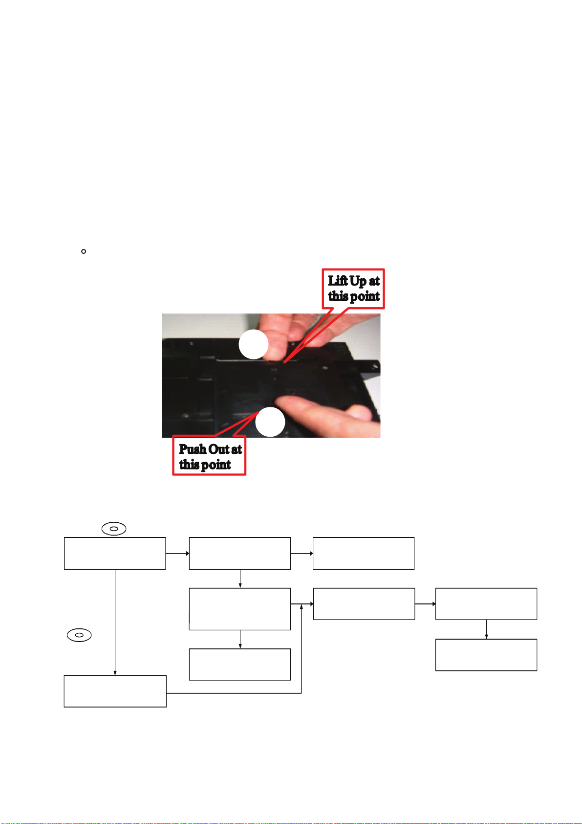
How to open FFC Holder. Refer below picture.
•
BDP-BX38/S280/S380/S383
1-4-2.
Checking Flow ~ Drive (BU) section ~
Drive flowchart
BLX-104
BDP-S380 can play the BD-disc
YES
DVD: HLX-513
CD: HLX-A1
NO
Check / replace the FFC cable, then check
1
1
2
2
1
2
Check Drive Power Supply
CN301 Pin 3: 12V
IC309 Pin 1: 5V
YES
BDP-S380 operates normally
OP FFC cable (1-838-615-11)
SPD FFC cable (1-838-617-11)
YES
OK
NO
NO
Check PS301, PS302
Replace PS when open
Check the Optical Block Unit (BU) by
service mode. (Flowchart zz)
BU IOP is OK?
NO
Replace the Optical Block Unit (BU)
Optical Block Unit (BU) replace
(Flowchart yy)
BDP-S380 can play the DVD/CD-disc
NO
1-15
Page 19
1-4-3. BU Check Flow [zz] ~
BDP-BX38/S280/S380/S383
Before
Optical Block Unit (BU) IOP check flow (zz) ~ [Before BU Replacement]
Enter Service Mode
<OPEN/CLOSE>., <PLAY>,<STOP>
Press
and plug in AC Power
Inside *Service Mode Menu
Select [8] Drive
Inside *Drive
Select [7] OP Check Menu
Inside *OP Check Menu
Select [2] dIOP then press 'ENTER'
Specification dIOP
+
BD: 3mA
-
DVD, CD: 3mA
AC Power OFF
1-4-4. BU (Optical Block) Repair Guide
+
-
YES
BU Replacement ~
NO
IOP out of specification need BU
replacement
Optical Block Unit (BU) replace
(Flowchart yy)
BDP 6G (BDP-S380) series component structure is as same as conventional DVD Players.
However BD player requires precise read out functions and also secure contents Protection
system.
Since above requirement, it is necessary to set/adjust BU data to EEPROM.
The following cases need Adjustments;
(1)Replace BU (MB is original)
(2)Replace MB (BU is original)
(3)Replace both BU and MB
•JIG Requirement
Digital camera (recommend with macro mode)
Barcode decoder (BDPRdec_ver2.0
) installed in JIG PC’s
USB memory
ESD work bench
•Procedure (all cases)
Refer the diagram
Remarks:
The servo adjustment procedure will be carried out during OP data Writing.
There is no manual adjustment procedure. LD ON TIME history doesn’t carry over.
Do not touch any optical block parts, Turn Table and during replacing. BD Laser diode
is very sensitive!
1-16
Page 20
1-4-5. BU Adjustment Flow [yy] ~
Optical Block Unit (BU) OP Data Write Flow (yy) ~ [After BU/MB Replacement]
BDP-BX38/S280/S380/S383
Remove the defective BU from Loading
Assy and also remove BU insulator (4pcs)
Unpack new BU and take OP Data Barcode
Assemble BU with Insulators to Loading
Decode the OP Data Barcode phot using
BDPRdec.exe
USB memory(File Name: BuData.txt)
Enter Service Mode and insert USB memory
And confirm dIOP by select [7] OP Check
photo by camera
Assy (tighten screw with 2kgf)
and save the test data to
to USB connector
Select [8] Drive -->
Select [1] Drive OP data Write
Press ENTER
After Finishing ReWrite OP data
--> Turn AC Power OFF
Menu to verify IOP in specification
The following cases need OP Data Write:
(1) Replace BU (MB is original)
(2) Replace MB (BU is original)
(3) Replace both BU and MB
JIG requirement
Digital camera (with macro mode)
Barcode decoder (BDPRdec.exe)
installed in jig
PC's (jig purpose)
USB memory
ESD free work bench
IOP in specification --> Turn AC Power OFF
Turn Power ON and check playback
performance using BD, DVD and CD
KEM-430AAA/C2RP Packing Spec.
1-4-6. KEM-470AAA/C2RP Packing Spec.
BLX-104
DVD: HLX-513
CD: HLX-A1
1-17
Page 21
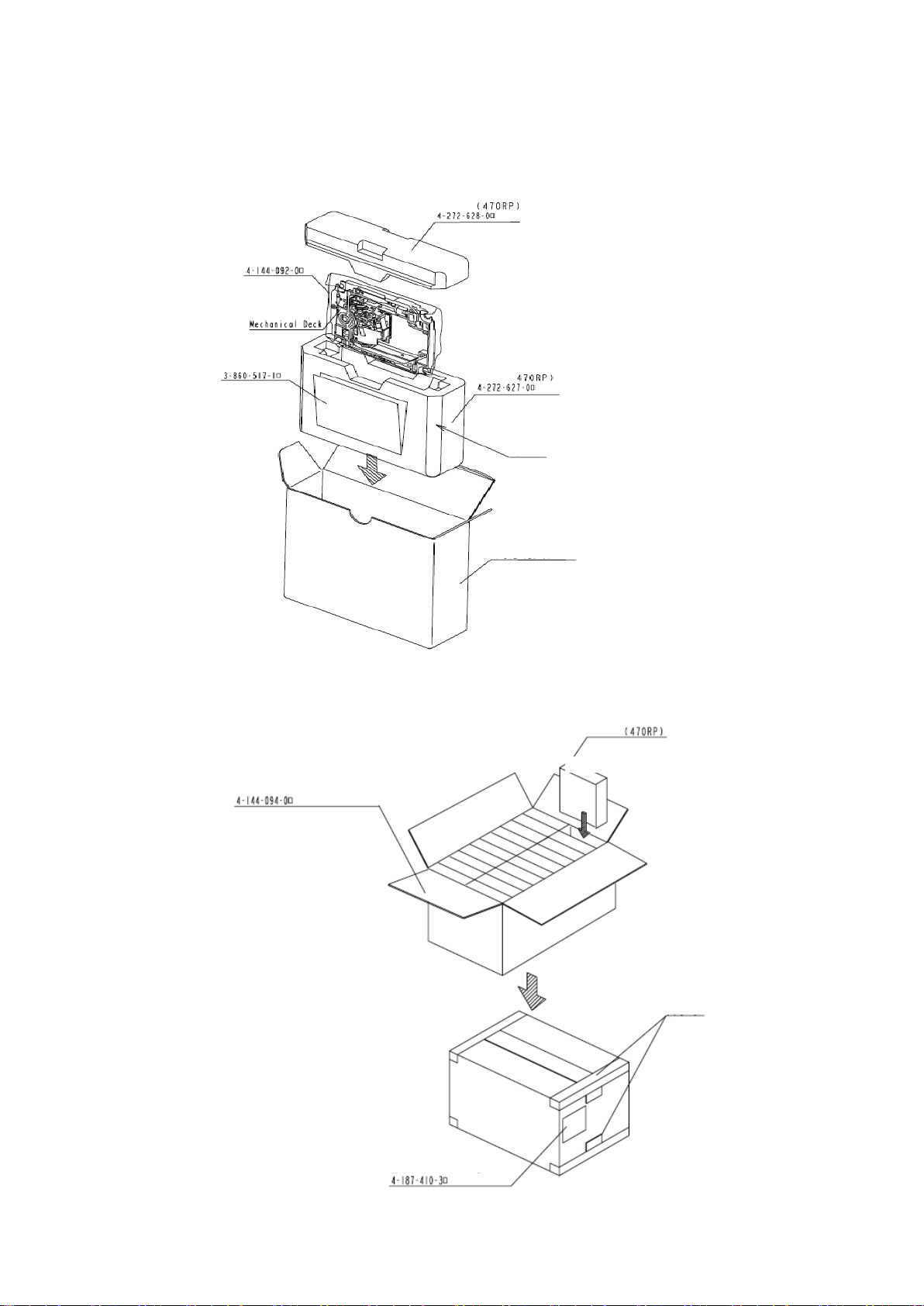
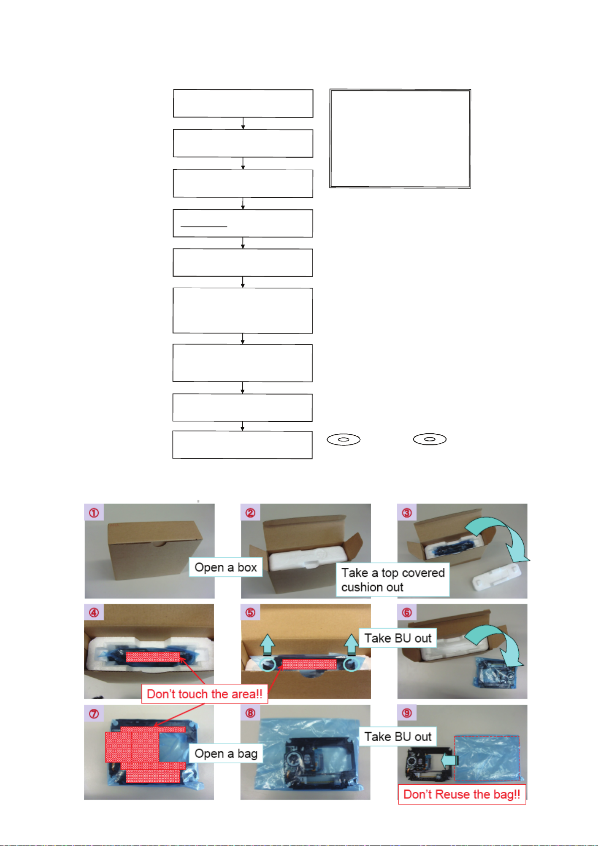
1-4-7. KEM-470AAA/C2RP Packing
BDP-BX38/S280/S380/S383
Lid foam tray
Instruction
Manual
Antistatic Bag
1) Store it in Cushion Carton
2) Store the Cushion carton in the individual carton
Cushion Carton
C surface cut facing front
Individual Carton (4-272-629-0)
Antistatic Bag
2) Store it in Individual Carton
3) Store it in Master Carton
Store 10 individual cartons 1 step X 2 steps
= 20 individual cartons in the master carton.
Master Carton (E430-BU-RP)
4) Master carton is sealed
with the PP tape.
Shipment Label
(Care Mark 3)
Individual Carton (E430-BU-RP)
PPTape
Stic
k it
toH.
1-18
Page 22

BDP-BX38/S280/S380/S383
BU Data Decode Jig
1-4-8. BU Data Decode Jig
・JIG Name: BDPRdec. exe
・
Release : 2010.11.26
・Version : 2.0.0.0
・Software Contents:
BDPRdec.exe ; Software
SavePath.ini ; decoded file destination setting file (initial destination is C:¥BuData.txt
Tasman.Bars.dll ; decode dll
Uninst.exe ; unistall BDPRd ec.exe from PC
・Installations
1.Unzip files to any PC Folder
2.Check the attached 2D code photo(OK_sample.JPG) drag-and-drop onto BDPRdec.exe, the
Password will be required at first time only, no need P/W from second time.
3.If there is the error message (.NET frame work requirements) please apply
Microsoft .NET Framework 2.0 (or 2.0 SP1) from Microsoft download site.
STEP 1
Microsoft .NET Framework Version 2.0 Redistributable Package (x86)
http://www.microsoft.com/downloads/details.aspx?displaylang=en&FamilyID=0856eacb-4362-4
8edd-aab15c5e04f5
)
b0d-
STEP 2
Microsoft .NET Framework 2.0 Service Pack 1 (x86)
http://www.microsoft.com/downloads/details.aspx?displaylang=en&FamilyID=79bc3b77-e02c-4
aacf-a7633f706ba5
*Hou to use
Case1
Drag-and-drop 2Dcode photo onto BDPRdec.exe
Case2
Drag-and-drop BU data file onto BDPRdec.exe
Data file name be changed to specify format and end of 7 character are defined
Player : ****BDP.txt
Recoder: ****BRD.txt
#You can also enter the file path at the prompt.
*Remarks
Do not change the decoded file name “BuData.txt”.
ad3-
1-19
Page 23
BDP-BX38/S280/S380/S383
Laser Caution Label
Loading For Service
1-4-9. Loading For Service
BDP 6G Loading Ass’y service parts consists from 3 parts.
①Holder, Clamper Assy
②Loading Assy
③Holder FFC
Currently these parts are producing 2 vendors. But the THERE IS NO COMPATIBILITY
So, please DO NOT MIX
“Loading for service” A-1750-926-A
the ① and ② of Loading for service and original Loading.
FFC
1-838-615-11
.
Laser Caution Label
Holder, Clamper Assy
①
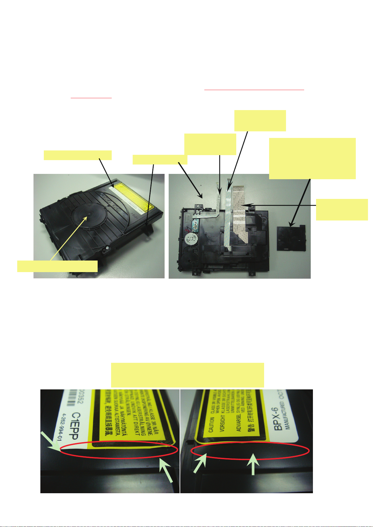
1-4-10. Laser Caution Label
The Loading Ass’y service parts does not have Laser Caution Label.
So that please reuse the original Laser Caution label and paste it on top of
1-838-619-11
②Loading Assy
FFC
③ Holder, FFC
4-167-321-01
(FFC Holder can be used
both service parts and original
parts)
FFC
1-838-617-11
new Loading Ass’y.
Limit Sample
Following peel off condition are acceptable
1-20
Page 24

BDP-BX38/S280/S380/S383
In case of BU assy replacement:
1. OP related data for new assy is controlled by BU factory
2. All of data is recorded into a barcode label
3. The label is put on the assy
4. Service parts will be followed
5. In service, the data should be read out from problem assy
6. The read data should be saved to new assy
Fact finding:
1. The label is “DATA MATRIX” format
2. The number of data is 91 words
3. The method of reading and saving is required when BU and
main board are replaced.
New service method
1. All of BU data on the barcode label is shot by digital camera in
order to make a JPEG file of BU data.
2. Application software in the PC makes digital data from JPEG file.
3. The converted data is stored to USB memory.
4. The USB memory is connected to BDP 6G unit.
5. In service mode, there is a command to save the data from USB
memory to board memory.
1-21
Page 25
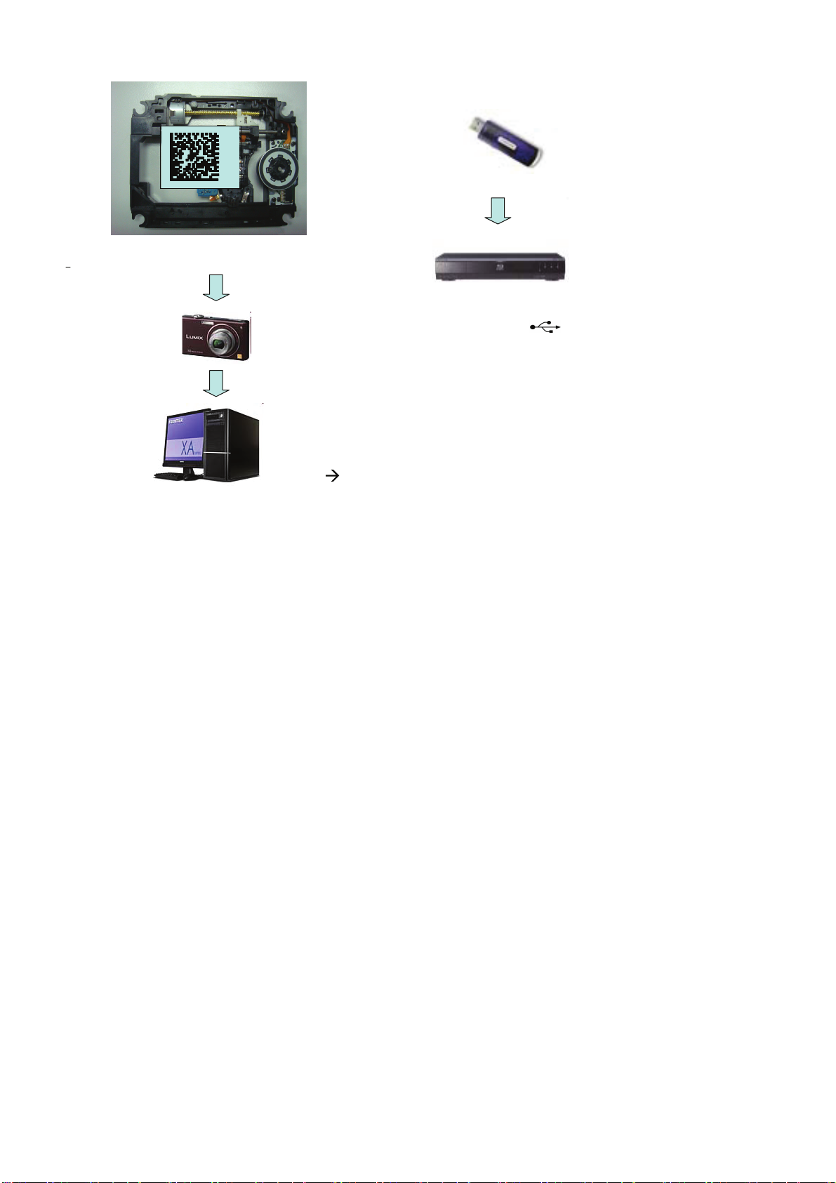
Shoot the barcode
Format is JPEG
Application Software
Data convert from
JPEG
TEXT
BDP-BX38/S280/S380/S383
Save the TEXT data
USB device is connected
to symbol on the
rear unit, and the TEXT
data as new data is
loaded to unit by service
mode.
The application software will be a service jig .
service jig, and the recording media will be CD-R.
Description: BDPRdec.exe
When instruction to PC, password is required.
The password will be supplied to only service HQ, and service center
name, q’ty and all of software registered information should be
maintained by service HQ, and Video will ask to report the registration
information.
1-22
Page 26
BDP-BX38/S280/S380/S383
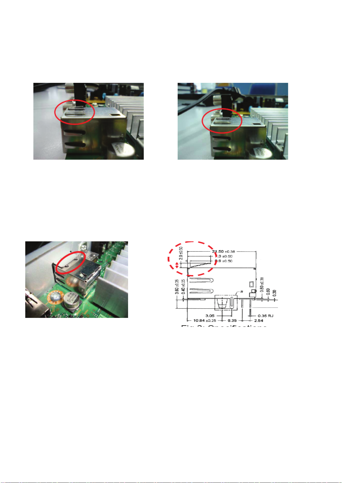
1-5.
REAR PANEL ASSEMBLY CAUTION
Whenever you need to assemble the rear panel, please make sure that the Ethernet connector (CN801)
Top Contact Springs are in good condition with height ≥2.0mm ± 0.5mm (refer to Fig 1)
Fig.1
If the Top Contact Springs are in at condition (Fig2), please lift them up to good condition
before assembling the rear panel.
Good Contact
Fig.2
When assembling the rear panel, please ensure good contact
between the Top Contact Springs to the rear panel.
1-23E
Spec.
Page 27
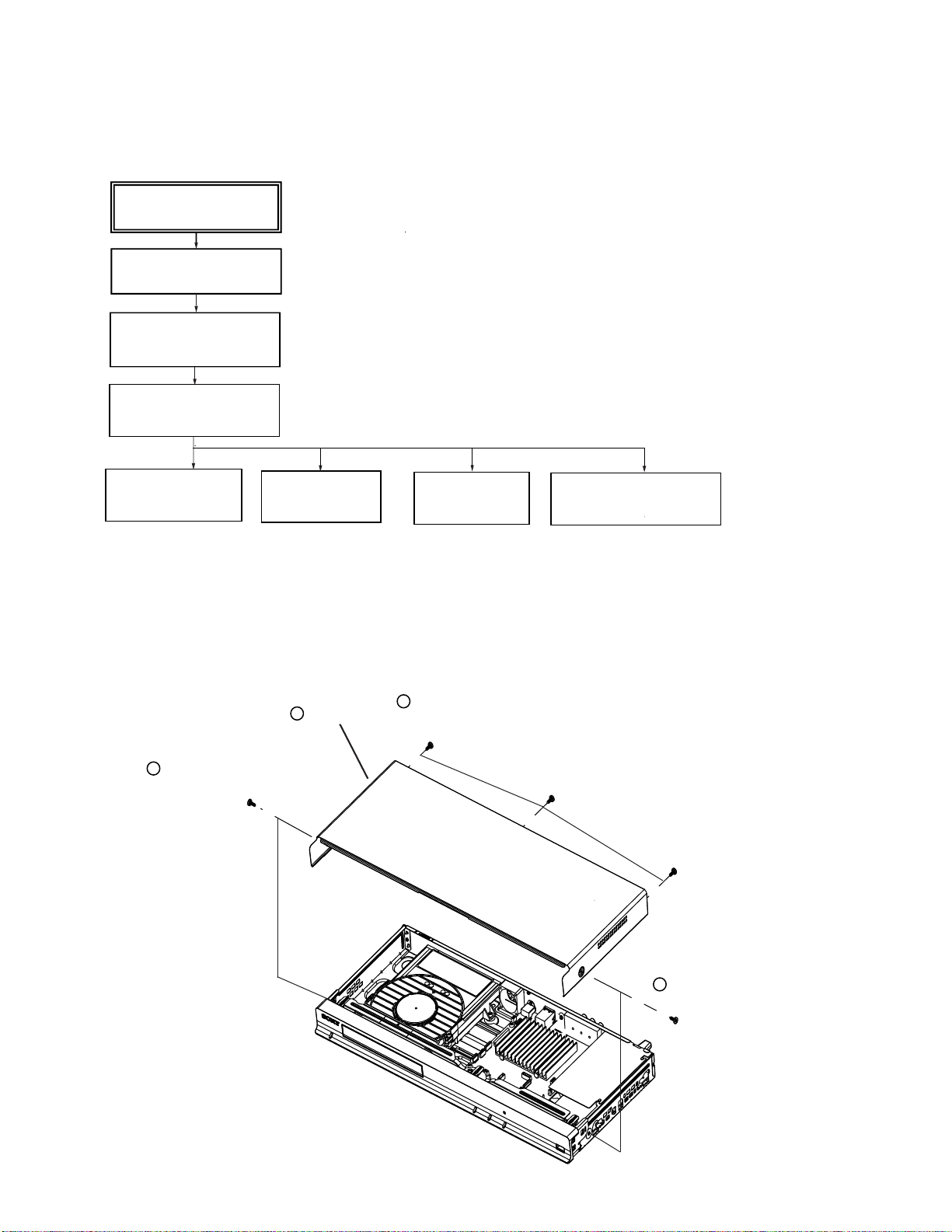
• This set can be disassembled in the order shown below.
2-1. DISASSEMBLY FLOW
SET
2-2. UPPER CASE
(Page 2-1)
2-3. TRAY COVER ASSY
(Page 2-2)
FRONT PANEL ASSY
FL-203 & IF-170 boards
2-4.
(Page 2-2)
BDP-BX38/S280/S380/S383
SECTION 2
DISASSEMBLY
2-5. REAR PANEL
(Page 2-3)
Note: Follow the disassembly procedure in the numerical order given.
2-6. MB-138 BOARD
(Page 2-3)
2-2. UPPER CASE
Three tapping screws
2
(tightening torque =
1 Tapping
(tightening torque =5 to 6
screw
Upper case
3
kgf•cm)
2-7.
BD DRIVE
(Page 2-4)
5 to6
2-8. SWITCHING REGULATOR
(Page 2-5)
kgf•cm)
2-1
tapping screw
1
(tightening torque = 5 to 6 kgf•cm)
Page 28
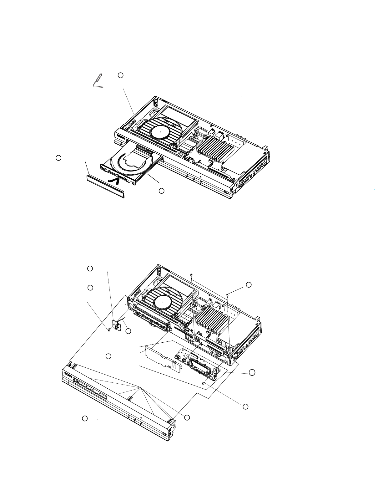
2-3. TRAY COVER ASSY
3 Tray cover assy
1 Insert a clip in the hole of a drive
to
open a tray.
tray
2
BDP-BX38/S280/S380/S383
2-4.
FRONT PANEL ASSY, FL-203 AND IF-170 BOARD
5
FL-203 Board
One screws
(tightening torque = 6 to 7 kgf•cm)
+BV3 (3-CR)
4
2
Front Panel
3
Harness (FLM-001)
CN331
Light guide
6
cover
Except BDP-S280
Eight hook
1
Two screws +BV3 (3-CR)
7
(tightening torque = 6 to 7 kgf•cm)
9
IF-170 Board
8
One screws
(tightening torque = 6 to 7 kgf•cm)
+BV3 (3-CR)
2-2
Page 29
2-5. REAR PANEL BLOCK
4
Rear panel block
Two screws+P 3X3
3
(tightening torque = 4 to 5 kgf•cm)
BDP-BX38/S280/S380/S383
2
Three ‘black’
(tightening torque = 6 to 7 kgf•cm)
1
PS Insulator top
screws +BV3(3-CR)
2-6. MB-138 BOARD
4
5
flexible flat
(CN2460)
6
flexible flat
(CN2470)
flexible flat
(CN1301)
cable (LDG-002)
cable (OPT-001)
cable (SPD-001)
Four screw s +BV3(3-CR)
7
(tightening torque = 6 to
8
MB-138 board
1 harness (PM-163)
(CN301)
7 kgf•cm)
3 harness (FLM-001)
(CN1203)
2-3
2 Flexible flat cable
(CN1204)
(FIM-031)
Page 30
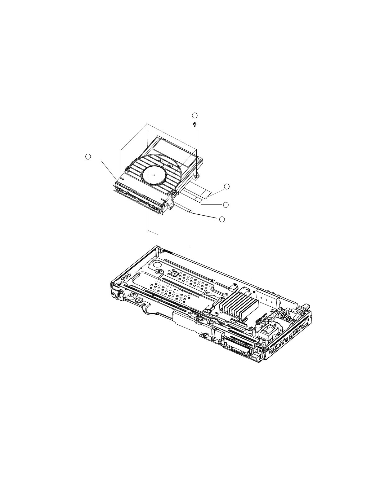
2-7. BD DRIVE
5 BD drive
four screws +BV3(3-CR)
1
(tightening torque = 6 to 7 kgf•cm)
2
Optical flexible flat cable (OPT-001)
(CN1301)
BDP-BX38/S280/S380/S383
Splindle flexible flat cable (SPD-001)
3
(CN2460)
4
Loading flexible flat cable (LDG-002)
(CN2470)
2-4
Page 31

2-8. SWITCHING REGULATOR
two screws +BV3(3-CR)
2
(tightening torque = 6 to 7
kgf•cm)
BDP-BX38/S280/S380/S383
2
PS Insulator top
3
switching regulator
2-9. CIRCUIT BOARDS LOCATION
FL-203 board
IF-170 board
MB-138 board
Switching Regulator
2-5E
Page 32

SECTION 3
BLOCK DIAGRAMS
3-1. OVERALL BLOCK DIAGRAM
BD DRIVE
DVD
Blu-ray
DRIVE
FL-203 BOARD
S331
POWER
MB-138 BOARD
IC1401
SA
DRIVE
IC2401
MOTOR
DRIVE
1Gb DDR3
B-BUS
A-BUS
IC106
IC206
IC107
FRONT
IC501
2G NAND
FLASH
USB
VIDEO
AUDIO
(ANALOG OUTPUT)
AUDIO
(DIGITAL OUTPUT)
IC101
MAIN SYSTEM CONTROL, DSP
SATA I/F, MEMORY CONTROL,
A/V OUT, HDMI, ETHERNET I/F,
USB I/F
CXD9997G-AB
HDMI
USB
REAR
IC1003
VIDEO AMP
IC907
AUDIO LINE
DRIVER
CN604
J901
HDMI OUT
USB
Y
COMPONENT
P
B
VIDEO OUT
R
P
VIDEO
L
AUDIO
R
COAXIAL
CN701
LINE OUT
DIGITAL OUT
PCM/DTS/DOLBY
DIGITAL
BDP-BX38/S280/S380/S383
EXCEPT:
BDP-S280
IF-170 BOARD
ND701
VACCUM
FLUORESCENT
DISPLAY
Q706,Q707
T701
CN201
DC/DC
CONVERTER
EXCEPT:
BDP-S280
S701
STOP
S702
PLAY
S703
OPEN/CLOSE
D709
(WHITE)
IC702
VFD DRIVER
IC703
REMOTE
CONTROL
RECEIVER
UNSW12V
VOLTAGE
DIVIDER
POWER-1
A
UNSW6V
IC1204
P FAIL
IC1203
SUB SYSTEM
CONTROL
PS1201
X401
27MHZ
DC DC 6V
ETHERNET
N801
C
)
(
L
A
N
1
0
0
CORE_1.1V
DCDC6V
SW5V
DCDC-4V
3.3VA
1.2VA
DDR3.1-5V
FE_SW12V
DAC3.3V
UNSW3.3V
REGULATOR
I
C
3
01
I
C
3
02
I
C
3
03
I
C
3
04
I
C
3
05
I
C
3
07
I
C
3
08
I
C
3
09
I
C
3
10
I
C
3
06
I
C
601
I
C
704
I
C
703
I
C
803
I
C
804
I
C
603
PS301
PS302
SWITCHING
REGULATOR
The components identifi ed by
mark
are critical for safety.
Replace only with part number
specifi ed.
(AC IN)
or dotted line with mark
3-1
Page 33

3-2. DSP BLOCK DIAGRAM
BD DRIVE
DVD
Blu -ray
DRIVE
23
22
26
25
32
30
28
20
31
33
19
17
34
39
38
37
CN1301
36
43
44
45
8
9
6
7
CN2460CN2470
4
3
2
1
2
3
5
MB-138 BOARD
BD_RF+
BD_RF-
DVD_RF +
DVD_RF-
A
B
C
D
E
F
G
H
SDIO
8
SCLK
7
LDD_SEN
6
THERMO
SA_B+
SA_B-
SA_A+
SA_A-
FD1
FR1
TR
TD
FD2
FR2
A
AB+
B-
U
V
W
LOAD LOAD+
TRAY-IN
TRAY-OUT
SYSCON_RST
PAGE 3-4
2740
2841
2942
30
24
25
55
56
52
53
42
44
46
33
32
STP1+
16
17
STP1-
18
STP2+
19
STP2-
FCS_P
FCS_N
TRK_P
TRK_N
TLT_P
TLT_N
SLED2_P
SLED2_N
SLED1_P
SLED1_N
U
V
W
LOAD_N
LOAD_ P
IC2401
MOTOR DRIVE
19
IC1401
SA_DRIVE
VFCS
VTRK
VSLED2
VSLED1
MONITOR
VSPIN
VLOAD
IC501
2Gb/16Gb
NAND FLASH
STP1_IN
STP2_IN
STEP_ENA
SA_B
8
SA_A
9
STEP_ENA
7
21 FOO
20 TRO
22
17
16
12
SPDL
18
NS_XTALO
NS_XTALI
19
CPU_NFD0 - CPU_NFD7
nCE
9
16
cLE
17
ALE
WE
18
8
nRE
7
RY/BY
J4
J3
J1
J2
E1
E2
F1
F2
H3
H4
G2
G1
P2
P1
R3
D3
N1
M4
N3
K2
K1
L4VTLT
L3
U4
Q4
M1
B12
A12
M3
W1
W2
C22
B22
D21
C21
A23
B23
RFIP
RFIN
RFIP2
RFIN2
INA
INB
INC
IND
INE
INF
ING
INH
FE CFREQ
FEOSCEN
FECMOD
AUX1
FE FM O4
FE FM O3
FE GAINSW2
TLO
FE FM O
FE FMO2
FE LIMIT
FEDM0
FE TR AYPWM
FETR
FETR
CPU_NFCEN
CPU_NFCLE
CPU_NFALE
CPU_NFWEN
CPU_NFREN
CPU_NFRBN
IC101
MAIN SYSTEM CONTROL,
DSP,SATA I/F,MEMORY CONTROL
A/V OUT,HDMI,ETHERNET I/F
USB I/F,
CXD9997G-AB
X401
27MHZ
AYIN_
AYOUT_
RBA0
RBA1
RBA2
RRAS
RCAS
R
RODT
RCLK0
RCLKB
RCLKE
RCS
RRESET
RCLK1
RCLK1
RBA0_B
RBA1_B
RBA2_B
RRAS_B
RCAS_B
RWE_B
RODT_B
RCLK0_B
RCLK0_B
RCKE_B
RCS_B
RRESET_B
BDP-BX38/S280/S380/S383
DODQ0-DODQ15
DOA0-DOA12
AD12
AC15
AC12
Y11
AA11
WE
AE12
AB11
AD22
AE22
AA14
AC11
Y14
DODQ16-DODQ31
AD10
AE10
DIDQ0-DIDQ15
DIA0-DIA12
M2
N8
M3
AJ41
AH40
AC43
AG41
AL43
AL41
AC41
AD42
Y25
M2
N8
M3
J3
K3
L3
K1
J7
K7
K9
L2
K1
M2
N8
M3
J3
K3
L3
K1
J7
K7
K9
L2
K1
M2
N8
M3
J3
K3
L3
K1
J7
K7
K9
L2
K1
IC106
1Gb DDR2
SDRAM
BA0
BA1
BA2
/RAS
/CAS
/WE
ODT
CK
/CK
CKE
/CS
/RESET
IC107
1Gb DDR2
SDRAM
BA0
BA1
BA2
/RAS
/CAS
/WE
ODT
CK
/CK
CKE
/CS
/RESET
IC106
1Gb DDR2
SDRAM
BA0
BA1
BA2
/RAS
/CAS
/WE
ODT
CK
/CK
CKE
/CS
/RESET
3-2
Page 34

BDP-BX38/S280/380/383
3-3. AV
MB-138 BOARD
OUT BLOCK DIAGRAM
C
01
I
1
SCL
SDA
D11
C11
C18
B19
C17
A19
D7
E8
Y
PB
PR
CVBS
XVMUTE
FORMAT1
VDACG_OUT
VDACB_OUT
VDACR_OUT
VDACX_OUT
PSD ,LORTNOC METSYS NIAM
F/I TENREHTE IMDH ,TUO V/A
LORTNOC YROMEM F/I ATAS
BA-G7999DXC
F/I BSU
AOMCLK/L
AOBCK/R
3
4
5
1
6
7
8
INL
1
10
INR
I
N
Y
P
I
B
N
N
RI
P
I
V
N
E 1
U
M
T
E 2
U
M
T
LPF SEL
C
00
1
I
3
I
E
D
O
M
A
V
P
IC907
AUDIO LINE
DRIVER
P
Y
O
P
B
O
PR
O
VO
OUTL
OUTR
J
01
9
7P JACK
12
U
T
U
T
1
0
UT
9
U
T
4
1
2
Y
B
P
R
P
VIDEO
L
COMPONENT
VIDEO OUT
LINE OUT
AUDIO
119
R
AMUTE
SPDIF
CH2_P
CH2_M
CH1_P
CH1_M
CH0_P
CH0_M
CLK_P
CLK_M
HTPLG
B13
A13
B15
A15
B16
A16
E23
C8
E9
B14
A14
T
P
2
X
TX2N
TX1P
TX1N
TX0P
TX0N
TCKP
TCKN
IFCON_XMUTE
MUTE
7
Q901
XAMUTE
T
P
2
X
TX2N
TX1P
TX1N
TX0P
TX0N
TCKP
TCKN
TMDS DATA2+
CN701
TMDS DATA2-
TMDS DATA1+
TMDS DATA1TMDS DATA0+
TMDS DATA0TMDS CLOCK+
TMDS CLOCK-
HPD
1
3
4
6
7
9
0
1
2
1
1
9
COAXIAL
HDMI OUT
DIGITAL OUT
PCM/DTS/DOLBY
DIGITAL
3-3
PAGE 3-4
22
IT-CON
CEC
Q702
CEC PULL-UP
ISOLATING SWITCH
CEC
3
1
Page 35

3-4. USB/ETHER BLOCK DIAGRAM
BDP-BX38/280/380/383
MB-138 BOARD
CXD9997G-AB
CN1102
J22
J23
AC4
GPIO4
AA5
GPIO5
CN1202
TXVN_0
TXVP_0
TXVN_1
TXVP_1
GPIO2
VSTB
GPIO1
GPIO6
DM DP
Y1
Y2
DM0
AB1
DP0
AB2
B4
A3
B5
A4
CN604
CN801
3
4
7
8
LAN (100)
USB
EXT
EXCEPT: BDP-S280
CN201
2
3
IF-170 BOARD
3
22221
11
13
15
9
8
16
19
5
3
21
23
1
2
22
14
10
FL-203 BOARD
CN331
1 1
CN702
D+
D-
DIN
S331
S701
S702
S703
IC703
REMOTE
CONTROL
RECEIVER
7
CLK
8
STB
9
IC702
VFD DRIVER
GRD1 - GRD8
SEG1 -SEG17
Q709
LED DRIVER
EXCEPT: BDP-S280
D709
(WHITE)
ND701
VACCUM
FLOURESCENT
DISPLAY
DM
DP
CN1204
IC1203
KEY1
KEY3
KEY2
KEYO
13
14
16
31
37
35
36
27
38
L22
K22
L23
B7
L21
A7
K23
AC3
48
47
49
3
30
43
51
25
LED_WHITE
33
RXD0
34
TXD0
12
8
SIRCS_IN
KEY1
KEY3
KEY2
LED_WHITE
CN1203
3-4
Page 36

D
C
D
C
4
V
S
W
5
V
3-5. PO WER BL OC K DIAG RA M
16-17
14
13
1
2
(AC IN)
1
2
7
APS-279(BDP-S280:EXCEPT US,CND/S380:EXCEPT US,CND/S383)
SRV2224UC(BX38/S280:US,CND/S380:US,CND)
4
SWITCHING REGULATOR :
5
6
3
UNSW12V
UNSW-12V
FE_GND_M
GND
FE-UNSW 12V
MB-138 BOARD
CN301
PS302
1
2
IC310
DCDC6V
PCONT1
7
4
CN301
5
6
PS301
3
IC 302
BDP-BX38/280/380/383
DDR3_1.5V
PCONT3
PCONT3
IC 501
NAND
FLASH
PCONT_CORE
PCONT3
IC305
+3.3V
REGULATOR
PCONT3
IC308
DDR3_1.5V
IC304
+1.2V
REGULATOR
IC306
+3.3V
REGULATOR
IC307
+1.1V
REGULATOR
IC704
+3.3V
REGULATOR
DAC 3.3 V
1.2V
3.3V
CORE_1.1V
AVDD33_HDMI
VOLTAGE
DIVIDER
ATA_PCONT1
VREF_0.75V
CPU1.2V
HDMI_1.2V
CPU-3.3VA
IC907
IC309
REGULATOR
1
1
1
1
1
AUDIO
LINE DRIVER
+5V
DDR3_1.5V
IC101
CXD9997G-AB
IC106
DDR3
SDRAM
IC107
DDR3
SDRAM
IC206
DDR3
SDRAM
1
USB_VBUS_PCONT1
Q303
Q302
FE_SW12V
DCDC4V
FE_SW5V
DCDC6V
DCDC6V
DCDC6V
DCDC6V
PCONT3
PCONT3
IC 301
+3.3V
REGULATOR
IC 601
REGULATOR
IC 603
+5V
REGULATOR
IC 705
+5V
REGULATOR
REGULATOR
IC 1361
+8V
REGULATOR
IC 2401
MOTOR
DRIVER
+5V
IC 303
+5V
UNSW3.3V
PCONT1
PCONT2
PCONT3
PCONT_CORE
AT
A_PCONT1
USB 5V
USB 5V
HDMI 5V
FR_6V
IC1003
VIDEO
BUFFER
PS1201
IC 1401
MOTOR
DRIVER
IC 1203
IF CON
3.3V
CN 1502
C
C
V
CN1204
IT_3.3V
8V
CN604
CN701
CN1401
CN1102
(IFCON FLASH WRITER)
USB
1
EXT
18
HDMI OUT
CN702
5
18
6
19
7-8
10
11
IF-170 BOARD
O
NISECON
1
8
T
P
D7019
LED WHITE
EXCEPT BDP-S280
R708
Q706,Q707
DCDC
CONVERTER
Q709
LED DRIVE
IC701
REMOTE CONTROL
RECEIVER
ND701
FLUORESENT
INICATOR
TUBE
D705,D706
RECT
IC702
VFD DRIVE
EXCEPT BDP-S280
USB
1
EXT
CN202
UNSW12V
PCONT3
UNSW12V
DCDC4V
FE-UNSW 12V
3 - 5E
SW3.3V
CN1101
ICE
1
8
The components identifi ed by
or dotted line with mark
mark
are critical for safety.
Replace only with part number
specifi ed.
Page 37

SECTION 4
SCHEMATIC DIAGRAMS
4-1. THIS NOTE IS COMMON FOR SCHEMATIC DIAGRAMS
All capaci tors are in F un les s otherwise noted. pF : F.
50V or less are not indicated except for electrolytics and tantalums.
All resistors are in ohms, 1/4 W (Chip resistors : 1 /10 W) un-less
otherwise specified.
=1000 , M =1000k .
k
% : indicates tolerance.
Caution when replacing chip parts.
New parts must be attached after removal of chip.
Be careful not to heat the minus side of tantalum capacitor, because
it is damaged by the heat.
Constants of resistors, capacitors, ICs and etc with XX indicate
that they are not used.
In such cases, the unused circuits may be indicated.
All variable and adjustable resistors have characteristic curve B,
unless otherwise noted.
: nonflammable resistor
: fusible resistor
: panel designation
f : internal component.
: adjustment for repair.
: B+ Line
: B– Line
Circled numbers refer to waveforms.
Voltages are dc between measurement point.
Readings are taken with a color-bar signals on Blu-ray disc.
Readings are taken with a digital multimeter (DC 10M ).
Voltage variations may be noted due to normal production tolerances.
BDP-BX38/S280/S380/S383
Note:
The componen ts ident ifi ed
by mark
with mark
safety.
Replace only with part number specified.
When indicating parts by reference number, please include the
board name.
or dotte d line
are critical for
Note:
Les composants identifiés par
une marque
pour la sécurité.
Ne les remplacer que par une
pièce portant le numéro spécifié.
sont critiquens
4-1
Page 38

BDP-BX38/S280/S380/S383
4-2.
FRAME SCHEMATIC DIAGRAM
1
2
A
B
C
D
E
BU
F
G
H
I
43
45P
CNXXX X
FR2
FD2
TD
TR
FR1
FD1
SA_B +
SA_B SA_A +
SA_A GND
THER MO
F
A
E
B
5V_P D
C
GND
DVD_ RF+
DVD_ RF-
GND
BD_R F+
BD_R FGND
D
G
VC_P D
H
GND
GND
GND
GND
5.0V
GND
8.0V
GND
SDIO
SCLK
SEN_ LDD
LDEN
TEST _V
MODE _A
MODE _B(2- ->3)
GND
CNxx x
9P
COMMON
CNxx x
5P
TRAY- IN
TRAY- OUT
FGND
LOAD -
LOAD +
98765
VBUSDM
DPGND
1 2 3 4
CN60 4
REAR
CN130 1
45P
OPT-0 01
1-838 -615 -11/ 21
FFC
SPD-0 01
1-838 -617 -11/ 21
FFC
LDG-0 02
1-838 -619 -11/ 21
FFC
1
2
MODE _B(2- ->3)
3
4
5
6
7
8
9
10
11
12
13
14
15
16
17
18
19
20
21
22
23
24
25
26
27
28
29
30
31
32
33
34
35
36
37
38
39
40
41
42
43
44
45
1
2
3
4
5
6
7
8
9
1
2
3
4
5
GND
MODE _A
TEST _V
LDEN
SEN_ LDD
SCLK
SDIO
GND
8.0V
GND
5.0V
GND
GND
GND
GND
H
VC_P D
G
D
GND
BD_R FBD_R F+
GND
DVD_ RFDVD_ RF+
GND
C
5V_P D
B
E
A
F
THER MO
GND
SA_A SA_A +
SA_B SA_B +
FD1
FR1
TR
TD
FD2
FR2
W
V
U
B
B/
A
A/
LOAD -
LOAD +
TRAY- IN
GND
TRAY- OUT
CN246 0
9P
NOMMOC
DNGF
CN247 0
5P
2P
CN120 3
KEY0(POWE R)
1
FLM-0 01
1-967 -315 -11/ 21
Harne ss
1
KEY0(POWE R)
CN33 1
2P
GND
2
2
GND
1
2
3
4
5
6
7
8
9
10
11
12
13
14
15
16
17
18
19
20
21
22
23
24
25
26
27
28
29
30
31
32
33
34
35
36
37
38
39
40
41
42
43
44
45
1
2
W
3
V
4
U
5
6
B
7
/B
8
A
9
/A
1
2
3
GND
4
5
4P
123456789
TMDS DATA 1 +
TMDS DATA 2 +
TMDS DATA 1 -
TMDS DATA 0 +
TMDS DATA 2 -
TMDS DATA 2 SH IELD
TMDS DATA 1 SH IELD
7P
CN120 2
NC
MODE
IF_RXD
IF_TXD
IFCON FLA SH W RITE R
GND
1234567
10111213141516171819202122
CEC
SCL
SDA
RESER VED
TMDS DATA 0 -
TMDS CLOC K +
TMDS CLOC K -
TMDS CLOC K SH IELD
TMDS DATA 0 SH IELD
23P
CN120 4
To I F
VCC
RESET
GND
USB_DP
123456789
123456789
KEY2(0/C)
KEY3(PLAY )
CN70 2
23P
23
HPD
+5V P OWER
PARTS BOD Y
PARTS BOD Y
PARTS BOD Y
DDC/C EC G ND
USB_DM
KEY1(STOP )
PARTS BOD Y
19P
CN70 1
HDMI
GND
USB_VBUS2
USB_VBUS1
GND
FLD_STB
FLD_SCK
GND
FLD_DIN
GND
IT_3.3V
LED_WHITE
FLD_PCONT
FIM-0 31
1-838 -618 -11/ 21
FFC
GND
IT_3.3V
FR_6V
GND
FLD_DIN
FLD_CLK
10111213141516171819202122
GND
10111213141516171819202122
GND
SIRCS
FR_6V
FR_6V
FLD_PCONT
LED_WHITE
10
CN80 1
ETHER NET
SERVO MON ITOR
CN139 1
6P
MPXOUT1
MPXOUT2
GND
MPXOUT3
GIO13
NISEC ON
CN138 1
6P
3.3V
GND
RXD
TXD
JIG_MODE0
JIG_MODE1
IFCON DEB UGGE R
CN120 1
5P
GND
MODE
VCC
RESET
NC
NISEC ON
CN110 2
6P
3.3V
GND
RXD
TXD
JIG_M ODE1
JIG_M ODE0
CN30 1
7P
UNSW1 2V
UNSW1 2V
FE_UN SW12 V
FE_GN D_M
GND
GND
UNSW- 12
FR_6V
GND
SIRCS
GND
KEY1(STOP )
KEY2(O/C)
KEY3(Play )
23
23
GND
GND
FLD_STB
GND
USB_DM
USB_DP
USB_VBUS1
USB_VBUS2
1
2
3
4
5
6
1
2
3
4
5
6
1
2
3
4
5
1
2
3
4
5
6
1
2
3
4
5
6
7
PM-16 3
1-967 -499 -11/ 21
Harne ss
11
12
13
14
AC OUT
CN10 1
2P
AC_IN (L)
SC_IN (N)
SWITCHING REGULATOR831-BMYSSA GNIDAOL DB
P/S
CNxx x
7P
UNSW1 2V
1
UNSW1 2V
2
FE_UN SW12 V
3
FE_GN D_M
4
5
GND
6
GND
7
UNSW- 12
FL-20 3
IF-17 0
J
4-2
Page 39

IF-170
4-3. BOARD (FRONT LEFT ) SCHEMATIC DIAGRAM • See page 5-3 for printed wiring board.
- Ref. No.: board; 20,000 series -
IF-170
BDP-BX38/S280/S380/S383
1
2
43
98765
10
11
12
13
14
A
B
C
D
E
F
G
H
I
J
by mark or dotted line with
mark
are critical for safety.
Replace only with part number
4-3
Page 40

BDP-BX38/S280/S380/S383
4-4. IF-170 BOARD (USB FRONT) SCHEMATIC DIAGRAM
- Ref. No.: IF-170 board; 20,000 series -
• See page 5-3 for printed wiring board.
2
31
IF-170 BOARD
A
B
4-4
Page 41

BDP-BX38/S280/S380/S383
4-5. FL-203 BOARD (POWER) SCHEMATIC DIAGRAM
- Ref. No.: FL-203 board; 20,000 series -
• See page 5-3 for printed wiring board.
2
31
FL-203 BOARD
A
B
4-5
Page 42

BDP-BX38/S280/S380/S383
4-6. MB-138 BOARD (DDR 3 A ) SCHEMATIC DIAGRAM (1/14) • Se
- Ref. No.: MB-138 board; 10,000 series
1
A
B
C
2
43
e page 5-4 for printed wiring board.
98765
10
11
12
13
14
D
E
F
G
H
I
J
4 6
Page 43

BDP-BX38/S280/S380/S3838
4-7. MB-138 BOARD (DDR 3 B) SCHEMATIC DIAGRAM (2/14) • Se
- Ref. No.: MB-138 board; 10,000 series
1
A
B
C
2
43
e page 5-4 for printed wiring board.
98765
10
11
12
13
14
D
E
F
G
H
I
J
4-7
Page 44

BDP-BX38/S280/S380/S3838
4-8. MB-138 BOARD (POWER)SCHEMATIC DIAGRAM (3/14) • Se
- Ref. No.: MB-138 board; 10,000 series
1
2
A
B
C
D
43
e page 5-4 for printed wiring board.
98765
10
11
12
13
14
E
F
G
H
I
J
The components identifi ed
by mark
mark
Replace only with part number
specifi ed.
4-8
or dotted line with
are critical for safety.
Page 45

BDP-BX38/S280/S380/S383
4-9. MB-138 BOARD (CLK/POWER) SCHEMATIC DIAGRAM (4/14) • Se
- Ref. No.: MB-138 board; 10,000 series
1
A
B
C
2
43
e page 5-4 for printed wiring board.
98765
10
11
12
13
14
D
E
F
G
H
I
J
4-9
Page 46

BDP-BX38/S280/S380/S383
4-10. .MB-138 BOARD (FLASH/HOST) SCHEMATIC DIAGRAM (5/14) • Se
- Ref. No.: MB-138 board; 10,000 series
1
A
B
C
D
2
43
e page 5-4 for printed wiring board.
98765
10
11
12
13
14
E
F
G
H
I
J
4-10
Page 47

BDP-BX38/S280/S380/S383
4-11. MB-138 BOARD (USB) SCHEMATIC DIAGRAM (6/14) • Se
- Ref. No.: MB-138 board; 10,000 series
1
A
B
C
D
2
43
e page 5-4 for printed wiring board.
98765
10
11
12
E
F
G
H
I
J
4-11
Page 48

BDP-BX38/S280/S380/S383
4-12. MB-138 BOARD (HDMI) SCHEMATIC DIAGRAM (7/14) • Se
- Ref. No.: MB-138 board; 10,000 series
1
A
B
C
D
2
43
e page 5-4 for printed wiring board.
98765
10
11
12
13
14
E
F
G
H
I
J
4-12
Page 49

BDP-BX38/S280/S380/S383
4-13. MB-138 BOARD (ETHERNET) SCHEMATIC DIAGRAM (8/14) • Se
- Ref. No.: MB-138 board; 10,000 series
1
A
B
C
D
2
43
e page 5-4 for printed wiring board.
98765
10
11
12
13
14
E
F
G
H
I
J
4-13
Page 50

4-14. MB-138 BOARD (AUDIO) SCHEMATIC DIAGRAM (9/14) • Se
- Ref. No.: MB-138 board; 10,000 series
-
e page 5-4 for printed wiring board.
BDP-BX38/S280/S380/S3838
1
A
B
C
D
E
2
43
98765
10
11
12
13
14
F
G
H
I
J
4-14
Page 51

4-15. MB-138 BOARD (VIDEO) SCHEMATIC DIAGRAM (10/
- Ref. No.: MB-138 board; 10,000 series
14)
• Se
e page 5-4 for printed wiring board.
BDP-BX38/S280/S380/S383
1
2
43
98765
10
11
12
13
14
A
B
C
1
2
0.32V
D
E
2.2V
0.32V
0.69V
3
0.69V
3.3V
3.3V
4
8
7
1.3V
5.0V
1.3V
0
1.9V
1.9V
0.0V
6
5
F
G
H
I
J
4-15
Page 52

4-16. MB-138 BOARD (GPIO/JTAG) SCHEMATIC DIAGRAM (11/
- Ref. No.: MB-138 board; 10,000 series
14)
• Se
e page 5-4 for printed wiring board.
BDP-BX38/S280/S380/S383
1
A
B
C
D
E
2
43
98765
10
11
12
13
14
F
G
H
I
J
4-16
Page 53

4-17. MB-138 BOARD (IFCON) SCHEMATIC DIAGRAM (12/
- Ref. No.: MB-138 board; 10,000 series
14)
• Se
e page 5-4 for printed wiring board.
BDP-BX38/S280/S380/S383
1
A
B
C
D
E
2
43
98765
10
11
12
13
14
F
G
H
I
J
4-17
Page 54

4-18. MB-138 BOARD (
- Ref. No.: MB-138 board; 10,000 series
FE_POWER/OP/GIO)
SCHEMATIC DIAGRAM (13/
14)
• Se
e page 5-4 for printed wiring board.
BDP-BX38/S280/S380/S383
1
A
B
C
D
E
2
43
98765
10
11
12
13
14
F
G
H
I
J
4-18
Page 55

4-19. MB-138 BOARD (FE_POWER_MOTOR DRIVE) SCHEMATIC DIAGRAM (14/
- Ref. No.: MB-138 board; 10,000 series
14)
• Se
e page 5-4 for printed wiring board.
BDP-BX38/S280/S380/S383
1
A
B
C
D
E
2
43
98765
10
11
12
13
14
F
G
H
I
J
4-19
Page 56

4
5
4-20. WAVEFORMS
MB-138 BOARD
BDP-BX38/S280/S380/S3838
IC1003
H
IC1003
IC1003
(VIN)IC1003
1
1.2 Vp-p
3
(PYIN)
(PBIN)
H
1.0 Vp-p
0.7Vp-p
H
IC1003
H
IC1003
H
IC101
(YOUT)
12
(VOUT)
14
A12
(NS_XTAL_I)
27 MHz
2.0Vp-p
2.4 Vp-p
Vpp
3.3 Vp-p
IC1003
IC1003
IC1003
(PRIN)
H
9
(PROUT)
10
(PBOUT)
H
0.7Vp-p
1.4Vp-p
H
1.4Vp-p
4-20E
Page 57

BDP-BX38/S280/S380/S383
SECTION 5
PRINTED WIRING BOARDS
5-1. THIS NOTE IS COMMON FOR PRINTED WIRING BOARDS
•
: Uses unleaded solders.
•
(The other layers’ patterns are not indicated)
• Through hole is omitted.
• There are few cases that the part printed on diagram isn’t mounted
•
• Chip parts.
: Pattern from the side which enables seeing.
Caution:
Pattern face side:
(SIDE B)
Parts face side:
(SIDE A)
in this model.
: panel designation
E BC3 1
Parts on the pattern face side seen from
the pattern face are indicated.
Parts on the parts face side seen from
the parts face are indicated.
Transistor Diode
5
524 6
6 5 4
1 2 3
5 4
1 2 3
2 1
3 4 5
3
2 132 132 1
5-1
Page 58

BDP-BX38/S280/S380/S383
5-2. FL-203 (REAR) BOARD PRINTED WIRING BOARD
- Ref. No.: FL-203 board; 20,000 series -
• See page 2-5 for circuit boards location.
: Uses unleaded solder.
There are a few cases that the part isn’t mounted in this model is printed on this diagram.
FL-203 BOARD (SIDE A)
A
1
FL-203 BOARD (SIDE A)
CN331 A-1
1-882-035-
2
11
5-2
Page 59

BDP-BX38/S280/S380/S383
5-3. IF-170 BOARD (FRONT RIGHT) PRINTED WIRING BOARD (SIDE A)
- Ref. No.: IF-170 board; 20,000 series -
: Uses unleaded solder.
IF-170 BOARD (SIDE A)
B
A
• See page 2-5 for circuit boards location.
There are a few cases that the part isn’t mounted in this model is printed on this diagram.
1-882-034-
11
IF-170 BOARD (SIDE A)
CN371 A-7
CN372 A-7
D702 A-1
D705 A-3
D706 A-3
D707 A-3
IC701 A-3
IC702 B-5
Q703 A-1
Q704 A-1
Q706 A-3
Q707 A-3
Q709 B-1
1
IF-170 BOARD (SIDE B)
B
A
2
43
5
6
7
1
2
1-882-034-
43
5-3
5
6
7
11
Page 60

DP-BX38/S280/S380/S383
B
5-4. MB-138 BOARD (MAIN) PRINTED WIRING BOARD (SIDE A) • See page 2-5 for circuit boards location.
- Ref. No.: MB-138 board; 10,000 series -
: Uses unleaded solder.
F
E
D
C
B
There are a few cases that the part isn’t mounted in this model is printed on this diagram.
MB-138 BOARD (SIDE A)
MB-134 BOARD (SIDE A)
CN301 B-6
CN302 A-5
CN303 A-6
CN601 C-2
CN602 C-2
CN701 G-3
CN901 F-1
CN902 F-2
CN904 G-1
CN1101 B-4
CN1102 E-6
CN1201 G-6
CN1320 F-1
CN1330 F-1
CN1382 B-2
CN1401 E-1
CN1424 D-2
CN1491 E-2
CN1501 A-5
CN1502 C-6
CN1503 G-1
CN1504 A-2
CN1505 A-3
CN1506 A-1
CN1507 A-2
CN1508 A-6
CN1509 C-6
CN1510 A-3
CN2460 C-1
CN2470 B-1
CN2490 B-1
D303 B-2
D304 C-6
D307 B-5
D603 D-2
D604 C-2
D605 C-2
D606 C-2
D701 G-3
D901 F-5
D904 G-5
D905 G-5
D906 G-2
D1001 G-4
D1002 G-5
D1003 G-4
D1004 G-5
D1201 F-6
IC101 D-4
IC104 C-3
IC105 C-5
IC204 D-5
IC205 E-5
IC306 F-5
IC307 F-2
IC501 E-6
IC502 E-5
IC701 G-2
IC901 G-5
IC1002 F-4
IC1003 F-4
IC1101 F-2
IC1102 F-2
IC1202 F-5
IC1390 E-2
IC1451 E-1
A-4
IC1502
IC1503 A-4
IC1504 B-4
IC2301 B-1
L301 B-5
L303 A-2
L304 B-6
L305 B-2
L603 C-3
L604 C-3
L605 C-3
L606 C-3
L607 C-2
L608 C-2
L701 G-3
L702 G-3
L703 G-3
L704 G-3
L1001 F-4
L1002 G-4
L1003 F-4
L2322 B-1
L232
4 B-1
Q909 G-1
Q1502 A-4
X401 E-4
X802 D-3
X1351 D-3
X1501 A-4
X1502 A-5
A
1
2
1-882-883-
43
5
6
11
5-4
Page 61

BDP-BX38/S280/S380/S383
5-6. MB-138 BOARD (MAIN) PRINTED WIRING BOARD (SIDE B)
- Ref. No.: MB-138 board; 10,000 series -
: Uses unleaded solder.
MB-138 BOARD (SIDE B)
• See page 2-5 for circuit boards location.
There are a few cases that the part isn’t mounted in this model is printed on this diagram.
A
B
C
D
MB-134 BOARD (SIDE B)
D302 F-5
D305 F-2
D306 E-6
D601 E-2
D602 F-2
D1501 F-3
IC301 F-6
IC302 F-5
IC303 B-3
IC304 A-4
IC305 B-4
IC308 F-5
IC309 F-2
IC310 E-6
IC311 E-5
IC312 E-1
IC601 E-2
IC602 F-3
IC702 B-3
IC703 A-3
IC704 A-3
IC705 A-2
IC1001 B-4
IC1201 B-6
IC1441 C-1
IC1501 A-1
IC1505 F-3
IC2401 D-1
IC2480 E-2
L302 E-5
L306 E-6
L1201 B-6
L1202 B-6
Q301 F-5
Q302 E-1
Q303 E-1
Q501 C-6
Q502 C-6
Q503 C-6
Q701 A-3
Q702 A-3
Q1501 A-1
Q1503 F-3
X1201 B-6
E
05
23456
1-882-883-
1
5-5E
11
Page 62

BDP-BX38/S280/S380/S383
e
A
A
A
A
A
A
A
A
A
L
A
A
A
A
A
r
A
A
A
A
y
A
A
A
L
A
A
L
A
A
L
A
A
y
A
A
L
A
t
A
A
A
A
A
A
A
A
A
A
A
A
A
A
SECTION 6
IC PIN FUNCTION DESCRIPTION
MAIN SYSTEM CONTROL PIN FUNCTION (MB-138 BOARD IC 101 : CXD9997G-AA)
J9 DVCC10_K Power 1.15 V digital power
J11 DVCC10_K Power 1.15 V digital power
J14 DVCC10_K Power 1.15 V digital power
J15 DVCC10_K Power 1.15 V digital power
J17 DVCC10_K Power 1.15 V digital power
K10 DVCC10_K Power 1.15 V digital power
K14 DVCC10_K Power 1.15 V digital power
K16 DVCC10_K Power 1.15 V digital power
L9 DVCC10_K Power 1.15 V digital power
L17 DVCC10_K Power 1.15 V digital power
M10 DVCC10_K Power 1.15 V digital power
M16 DVCC10_K Power 1.15 V digital power
N9 DVCC10_K Power 1.15 V digital power
N17 DVCC10_K Power 1.15 V digital power
P10 DVCC10_K Power 1.15 V digital power
P16 DVCC10_K Power 1.15 V digital power
R9 DVCC10_K Power 1.15 V digital power
R17 DVCC10_K Power 1.15 V digital power
T10 DVCC10_K Power 1.15 V digital power
T12 DVCC10_K Power 1.15 V digital power
T14 DVCC10_K Power 1.15 V digital power
T16 DVCC10_K Power 1.15 V digital power
U9 DVCC10_K Power 1.15 V digital power
U11 DVCC10_K Power 1.15 V digital power
U13 DVCC10_K Power 1.15 V digital power
U15 DVCC10_K Power 1.15 V digital power
U17 DVCC10_K Power 1.15 V digital power
N18 DVCC18_IO_1 Power 1.8 V / 1.5 V digital IO power
N23 DVCC18_IO_1 Power 1.8 V / 1.5 V digital IO power
T18 DVCC18_IO_1 Power 1.8 V / 1.5 V digital IO power
T23 DVCC18_IO_1 Power 1.8 V / 1.5 V digital IO power
V9 DVCC18_IO_1 Power 1.8 V / 1.5 V digital IO power
V12 DVCC18_IO_1 Power 1.8 V / 1.5 V digital IO power
V14 DVCC18_IO_1 Power 1.8 V / 1.5 V digital IO power
V16 DVCC18_IO_1 Power 1.8 V / 1.5 V digital IO power
V18 DVCC18_IO_1 Power 1.8 V / 1.5 V digital IO power
W23 DVCC18_IO_1 Power 1.8 V / 1.5 V digital IO power
B20 DVCC18_IO_1 Power 1.8 V / 1.5 V digital IO power
B21 DVCC18_IO_1 Power 1.8 V / 1.5 V digital IO power
C7 DVCC18_IO_1 Power 1.8 V / 1.5 V digital IO power
C10 DVCC18_IO_1 Power 1.8 V / 1.5 V digital IO power
C13 DVCC18_IO_1 Power 1.8 V / 1.5 V digital IO power
C17 DVCC18_IO_1 Power 1.8 V / 1.5 V digital IO power
Y21
W21
B24 TN_MEMPLL
B25 TN_MEMPLL
K19
E13
F13
F14
L20
C14
E13
F12
E12
L19
D14
12 NS_XTALI O 27MHz Crystal Ou
B12 NS_XTALO I 27MHz Crystal In
D12 TN_PLLG
C12 TP_PLLG
C8
C11
E11
D11
10
F11
B10
C10
VDD12_MEM PLL Power 1.15V Analog Power for MEMPLL
VSS12_MEM PLL Ground
VDD10_LDO Power 1.0V standby powe
VDD12_27MP LL Power 1.15V Analog Power for PLL
VDD12_APLL Power 1.15V Analog Power for APLL
VDD12_DMP LL Power 1.15V Analog Power for DMPLL
VDD33_LDO Power 3.3V power for standb
VDD33_XTAL Power 3.3V Analog Power for XTAL
VSS12_27MPLL Ground
VSS12_AP LL Ground
VSS12_DMPLL Ground
VSS33_LDO Ground
VSS33_XTAL Ground
OSDATA0 I/O
OSDATA1 I/O
OSDATA2 I/O
OSDATA3 I/O, 5V
pyTlobmySniP
nalog Test Pin
nalog Test Pin
nalog Test Pin
nalog Test Pin
O/I ETUM
O/IKCBO
O/IKCRLO
O/IKCLMO
Description
nalog Ground for MEMPL
nalog Ground for PL
nalog Ground for APL
nalog Ground for DMPL
nalog ground for standb
nalog ground for XTA
udio mute
udio out right Channel
NC
udio out left Channel
NC
NC
NC
NC
dnuorg latigiD dnuorG DNGD12E ,22D
dnuorg latigiD dnuorG DNGD22F ,12F
dnuorg latigiD dnuorG DNGD61J ,01J
dnuorg latigiD dnuorG DNGD11K ,9K
dnuorg latigiD dnuorG DNGD51K ,31K
dnuorg latigiD dnuorG DNGD01L ,71K
dnuorg latigiD dnuorG DNGD21L ,11L
dnuorg latigiD dnuorG DNGD41L ,31L
dnuorg latigiD dnuorG DNGD61L ,51L
dnuorg latigiD dnuorG DNGD11M ,9M
6-1
Page 63

A
A
A
A
A
r
A
r
A
X
r
A
A
A
A
A
A
A
A
t
A
t
A
t
A
A
t
A
r
A
r
A
r
A
r
A
A
A
A
A
A
BDP-BX38/S280/S380/S383
dnuorg latigiD dnuorG DNGD31M ,21M
dnuorg latigiD dnuorG DNGD51M ,41M
dnuorg latigiD dnuorG DNGD01N ,71M
dnuorg latigiD dnuorG DNGD21N ,11N
dnuorg latigiD dnuorG DNGD41N ,31N
dnuorg latigiD dnuorG DNGD61N ,51N
dnuorg latigiD dnuorG DNGD9P ,22N
dnuorg latigiD dnuorG DNGD21P ,11P
dnuorg latigiD dnuorG DNGD41P ,31P
dnuorg latigiD dnuorG DNGD71P ,51P
1R ,21R
J12 DGND_PWM Ground Digital ground for PWM
J13 DGND_PWM Ground Digital ground for PWM
K12 DGND_PWM Ground Digital ground for PWM
M7 DVCC33_IO Power 3.3 V digital IO power
N7 DVCC33_IO Power 3.3 V digital IO power
P7 DVCC33_IO Power 3.3 V digital IO power
Y7 DCC33_IO_2 Power 3.3 V digital IO power
E20 DVCC33_IO_3 Power 3.3 V digital IO power
F19 DVCC33_IO_3 Power 3.3 V digital IO power
G12 DVCC33_IO_6 Power 3.3 V digital IO power
G10 DVCC33_IO_P WM Power 3.3 V digital IO power for PWM
G11 DVCC33_IO_P WM Power 3.3 V digital IO power for PWM
J20 DVCC33_IO_S TB Power 3.3 V digital IO power for Stand-By Module
J21 DVCC33_IO_S TB Power 3.3 V digital IO power for Stand-By Module
E10 AOSDATA4 I/O, 5V
D10 AOSDATA5 I/O, 5V
O/IFIDPS 9E
C19
D17
D19
E18
E17
E19
D18 FS
B19 VDACB_OUT
C18 VDACG_OUT
C17 VDACR_OUT
19 VDACX_OUT
J24 GPIO8 /VOUTCLK1 I/O, 5V
E24 ETTXER /VOUTD0 I/O
E25 ETRXER /VOUTD1 I/O
G22 ETTXD0 /VOUTD10 I/O
G21 ETTXD1 /VOUTD11 I/O
H20 ETTXD2 /VOUTD12 I/O
H23 ETTXD3 /VOUTD13 I/O
H22 ETTXEN /VOUTD14 I/O
K20 ETCOL /VOUTD15 I/O
F23 ETCRS /VOUTD2 I/O
F24 ETRXDV /VOUTD3 I/O
F25 ETRXD0 /VOUTD4 I/O, 5V
G20 ETRXD1 /VOUTD5 I/O, 5V
H21 ETRXD2 /VOUTD6 I/O, 5V
G24 ETRXCLK /VOUTD7 I/O, 5V
G25 ETRXD3 /VOUTD8 I/O, 5V
G23 ETTXCLK /VOUTD9 I/O
K25 ETMDIO /VOUTHSYNC I/O
J25 ETMDC /VOUTVSYNC I/O
C15
D15
C16
D16
E15
F15
E16
VDD33_VDA C_BG Power 3.3V Analog Powe
VDD33_VDA C_R Power 3.3V Analog Powe
VDD33_VDA C_
VSS33_VDAC _BG Ground
VSS33_VDAC _R Ground
VSS33_VDAC _X Ground
VDD12_HDMI Power 1.15V Analog Powe
VDD12_HDMI Power 1.15V Analog Powe
VDD33_HDMI Power 3.3V Analog Powe
VDD33_HDMI Power 3.3V Analog Powe
VSS12_HDMI Ground
VSS12_HDMI Ground
VSS33_HDMI Ground
Power 3.3V Analog Powe
nalog DAC full scale
nalog DAC outpu
nalog DAC outpu
nalog DAC outpu
nalog DAC outpu
V5 ,O/INICM9D
V5 ,O/IKCBPS 01F
V5 ,O/IATADPS9B
V5 ,O/I KCRLPS9A
V5 ,O/I KLCMPS9C
NC
NC
NC
NC
NC
SPDIF out
NC
NC
nalog Ground
nalog Ground
nalog Ground
Nand Write protect (NC)
NC
NC
NC
NC
NC
NC
NC
NC
NC
NC
NC
NC
NC
NC
NC
NC
NC
NC
nalog Ground
nalog Ground
nalog Ground
dnuorg latigiD dnuorG DNGD11R ,01R
dnuorg latigiD dnuorG DNGD3
dnuorg latigiD dnuorG DNGD51R ,41R
dnuorg latigiD dnuorG DNGD9T ,61R
dnuorg latigiD dnuorG DNGD31T ,11T
dnuorg latigiD dnuorG DNGD71T ,51T
dnuorg latigiD dnuorG DNGD01U ,22T
dnuorg latigiD dnuorG DNGD41U ,21U
dnuorg latigiD dnuorG DNGD22W ,61U
dnuorg latigiD dnuorG DNGD8Y ,6Y
dnuorg latigiD dnuorG DNGD7AA ,6A
dnuorg latigiD dnuorG DNGD7BA ,02A
dnuorg latigiD dnuorG DNGD31BA ,01B
dnuorg latigiD dnuorG DNGD12CA ,71B
6-2
Page 64

A
A
A
A
A
A
A
A
A
A
A
A
A
A
A
A
A
A
A
A
A
A
A
A
A
A
A
A
k
A
A
t
A
t
A
BDP-BX38/S280/S380/S383
03 tib atad yromeM O/I 03QDR9C
13 tib atad yromeM O/I 13QDR 9B
0 tib ksam atad yromeM O 0MQDR 71Y
1 tib ksam atad yromeM O 1MQDR81B
2 tib ksam atad yromeM O 2MQDR 8B
3 tib ksam atad yromeM O 3MQDR 8C
noitarbilac revird pihc-nO I NDTXER 32E
W12 RVREF_1 I Memory VREF
Y19 RVREF_1 I Memory VREF
teser yromeM O TESERR 41Y
D23 RCAS__B O Memory column address strobe
M24 RCLK0_B O Memory clock 0 positive
M25 RCLK0__B O Memory clock 0 negative
P23 RDQ10_B I/O Memory data bit 10
P22 RDQ11_B I/O Memory data bit 11
P20 RDQ12_B I/O Memory data bit 12
R20 RDQ13_B I/O Memory data bit 13
R21 RDQ14_B I/O Memory data bit 14
P21 RDQ15_B
T2
1 RDQM0_B O Memory data mask bit 0
T20 RDQM1_B O Memory data mask bit 1
P24 RDQS0_B I/O Memory positive data strobe bit 0
P25 RDQS0__B I/O Memory negative data strobe bit 0
N25 RDQS1_B I/O Memory positive data strobe bit 1
N24 RDQS1__B I/O Memory negative data strobe bit 1
C23 RRAS__B O Memory row address strobe
R19 RVREF_3 I Memory VREF
Y25 RRESET_B O Memory reset
D23 HDMISCK I/O, 5V
I/O Memory data bit 15
V5 ,O/I CEC02F
V5 ,O/I 0OIPG8D
V5 ,O/I1OIPG 7A
V5 ,O/I 2OIPG 7B
V5 ,O/I 3OIPG 7C
V5 ,O/I 4OIPG4CA
V5 ,O/I 5OIPG5AA
V5 ,O/I 6OIPG 3CA
V5 ,O/I7OIPG 4BA
V5 ,O/IDSIMDH 22E
V5 ,O/IGLPTH 32E
NC
Syscon Req (IFCON)
Start Bit (IFCON)
XIF_CS(IFCON)
NC
NC
NC
UPG_STATUS
USB_Vbus_Pcont
HDMI I2C Clock
HDMI I2C Data
HDMI Hot Plug
teser ECI GATJ O/I _TSRT 1E
eborts sserdda wor yromeM O _SARR 11Y
elbane etirw yromeM O _EWR 21E
0 tib sserdda yromeM O B_0AR 32B
1 tib sserdda yromeM O B_1AR 22V
2 tib sserdda yromeM O B_2AR 52C
3 tib sserdda yromeM O B_3AR 42C
4 tib sserdda yromeM O B_4AR 32V
5 tib sserdda yromeM O B_5AR 32A
6 tib sserdda yromeM O B_6AR 42U
7 tib sserdda yromeM O B_7AR 22Y
8 tib sserdda yromeM O B_8AR 52U
9 tib sserdda yromeM O B_9AR 32Y
01 tib sserdda yromeM O B_01AR 42W
11 tib sserdda yromeM O B_11AR 32U
21 tib sserdda yromeM O B_21AR 52W
31 tib sserdda yromeM O B_31AR 42Y
0 tib sserdda knab yromeM O B_0ABR 52D
1 tib sserdda knab yromeM O B_1ABR 22U
2 tib sserdda knab yromeM O B_2ABR 22C
elbane kcolc yromeM O B_EKCR 12V
tceles pihc yromeM O B__SCR 42D
0 tib atad yromeM O/I B_0QDR 12U
1 tib atad yromeM O/I B_1QDR 02U
2 tib atad yromeM O/I B_2QDR 42T
3 tib atad yromeM O/I B_3QDR 52T
4 tib atad yromeM O/I B_4QDR 02M
5 tib atad yromeM O/I B_5QDR 32M
6 tib atad yromeM O/I B_6QDR 22M
7 tib atad yromeM O/I B_7QDR 12M
8 tib atad yromeM O/I B_8QDR 22R
9 tib atad yromeM O/I B_9QDR 32R
elbane etirw yromeM O B__EWR 52E
0 tib eborts atad evitisop yromeM O/I 0SQDR 91D
0 tib eborts atad evitagen yromeM O/I _0SQDR 91E
1 tib eborts atad evitisop yromeM O/I 1SQDR 02E
1 tib eborts atad evitagen yromeM O/I _1SQDR 02D
2 tib eborts atad evitisop yromeM O/I 2SQDR 6D
2 tib eborts atad evitagen yromeM O/I _2SQDR 6E
3 tib eborts atad evitisop yromeM O/I 3SQDR 7E
3 tib eborts atad evitagen yromeM O/I _3SQDR 7D
elbane noitanimret eid no yromeM O TDOR 11B
elbane noitanimret eid no yromeM O B_TDOR 42E
colc nacs yradnuob GATJ / kcolc ECI GATJ O/I KCT 2C
ni atad nacs yradnuob GATJ / ni atad ECI GATJ O/I IDT2D
uo atad nacs yradnuob GATJ / tuo atad ECI GATJ O/I ODT 1C
celes edom yradnuob GATJ / tceles edom ECI GATJ O/I SMT1D
6-4
Page 65

F16
A
A
A
A
A
A
A
A
A
A
A
A
A
A
A
A
A
A
A
A
A
A
A
A
A
A
A
A
A
A
A
A
A
A
A
A
A
A
A
A
A
A
A
A
A
A
A
A
A
A
A
A
A
A
A
A
A
A
A
A
A
A
A
A
A
15 CH0_M
14 CH1_M
B14 CH1_P
13 CH2_M
B13 CH2_P
16 CLK_M
B16 CLK_P
17 EXT_CAP
B17 EXT_RES
VSS33_HDMI Ground
BDP-BX38/S280/S380/S383
nalog HDMI TX data 0 differential pair (M)
nalog HDMI TX data 1 differential pair (M)
nalog HDMI TX data 1 differential pair (P)
nalog HDMI TX data 2 differential pair (M)
nalog HDMI TX data 2 differential pair (P)
nalog HDMI TX clock differential pair (M)
nalog HDMI TX clock differential pair (P)
nalog HDMI AIO
nalog HDMI reference voltage
O/I KCFS 02C
O/I SCFS 02A
O/I IDFS02B
O/IODFS 02D
O/I ELAFN 12D
O/I NECFN 22C
O/I2NECFN 22A
O/I ELCFN 22B
O/I 0DFN 32C
O/I 1DFN52A
O/I 2DFN 42B
O/I3DFN 52B
O/I4DFN 42C
O/I 5DFN 52C
O/I 6DFN 42D
O/I 7DFN 52D
O/INBRFN 32B
O/I2NBRFN 42
O/I NERFN32A
O/I NEWFN12C
nalog Ground
NC
NC
NC
NC
NAND Flash address latch enable
NAND Flash chip enable
NC
NAND Flash command latch enable
NAND Flash Data input/output bit0
NAND Flash Data input/output bit1
NAND Flash Data input/output bit2
NAND Flash Data input/output bit3
NAND Flash Data input/output bit4
NAND Flash Data input/output bit5
NAND Flash Data input/output bit6
NAND Flash Data input/output bit7
NAND Flash ready/busy
NC
NAND Flash read enable
NAND Flash write enable
0 tib sserdda yromeM O 0AR 21A
1 tib sserdda yromeMO1AR 51B
2 tib sserdda yromeM O2AR 31E
3 tib sserdda yromeM O3AR21B
4 tib sserdda yromeM O 4AR 51A
5 tib sserdda yromeM O 5AR 21Y
6 tib sserdda yromeM O 6AR 61Y
7 tib sserdda yromeM O 7AR 31D
8 tib sserdda yromeM O 8AR61A
9 tib sserdda yromeM O 9AR41C
01 tib sserdda yromeM O 01AR 41D
11 tib sserdda yromeM O 11AR 51Y
21 tib sserdda yromeM O 21AR 41E
31 tib sserdda yromeM O 31AR 41B
0 tib sserdda knab yromeM O 0ABR 21D
1 tib sserdda knab yromeM O 1ABR 51C
2 tib sserdda knab yromeM O 2ABR 21C
elbane kcolc yromeM O EKCR 41A
tceles pihc yromeM O _SCR 11C
0 tib atad yromeM O/I 0QDR61E
1 tib atad yromeM O/I 1QDR 61D
2 tib atad yromeM O/I 2QDR 61C
3 tib atad yromeM O/I 3QDR 61B
4 tib atad yromeM O/I 4QDR 12D
5 tib atad yromeM O/I 5QDR12E
6 tib atad yromeM O/I 6QDR02C
7 tib atad yromeM O/I 7QDR 81Y
8 tib atad yromeM O/I 8QDR 71E
9 tib atad yromeM O/I 9QDR 71D
01 tib atad yromeM O/I 01QDR 81C
11 tib atad yromeM O/I 11QDR71A
21 tib atad yromeM O/I 21QDR 91A
31 tib atad yromeM O/I 31QDR 91C
41 tib atad yromeM O/I 41QDR 81A
51 tib atad yromeM O/I 51QDR91B
61 tib atad yromeM O/I 61QDR 3D
71 tib atad yromeM O/I 71QDR4D
81 tib atad yromeM O/I 81QDR 3E
91 tib atad yromeM O/I 91QDR 4E
02 tib atad yromeM O/I 02QDR 01A
12 tib atad yromeM O/I 12QDR 01Y
22 tib atad yromeM O/I 22QDR 9Y
32 tib atad yromeM O/I 32QDR 9A
42 tib atad yromeM O/I 42QDR 6B
52 tib atad yromeM O/I 52QDR5B
62 tib atad yromeM O/I 62QDR 5C
72 tib atad yromeM O/I 72QDR 6C
82 tib atad yromeM O/I 82QDR9E
92 tib atad yromeM O/I 92QDR 9D
eborts sserdda nmuloc yromeM O _SACR 11A
evitisop 0 kcolc yromeM O 0KLCR22D
evitagen 0 kcolc yromeM O _0KLCR22E
evitisop 1 kcolc yromeM O 1KLCR01D
evitagen 1 kcolc yromeM O _1KLCR 01E
)P( riap laitnereffid 0 atad XT IMDHgolanA P_0HC 51B
6-3
Page 66

t
t
A
A
A
A
A
A
A
g
A
g
A
g
A
AA3A
A
A
AA4A
A
A
A
A
A
A
A
A
A
A
A
A
r
A
r
A
r
A
A
A
A
r
A
A
A
A
A
A
A
A
A
5
A
A
r
A
A
A
A
A
A
A
A
A
A
A
A
A
A
A
A
A
A
A
A
A
A
A
A
A
A
A
A
A
A
A
r
A
A
t
_
A
t
A
t
A
t
A
A
t
A
A
t
BDP-BX38/S280/S380/S383
V5 ,O/I RI 12K
V5 ,O/I DRDCL22K
V5 ,O/I DXRAU 22J
V5 ,O/IDXTAU 32J
V5 ,O/I KLCV32L
V5 ,O/I ATADV 22L
V5 ,O/I BTSV 12L
V5 ,O/I LCS 7D
V5
Y3
W5
Y4
Y1 USB_DM
Y2 USB_DP
W3 USB_VRT_1P
W4
W6
B1 USB_DM0
A1 USB_DM1
B2 USB_DP0
B3 USB_VRT
D4
C5
C6
E6
D5
D6
E7
F7
F9
F8
3 TXVP_0
B4 TXVN_0
5 REXT
B5 TXVN_1
6 TANA_1
B6 TANA_0
J6
J5
L5
F5
L6
D3
E5
K3
H5
K4
P2 FECFREQ 3.3V LVTTL Frequency selection signal output, or LDD serial interface data
M1 FEDMO
T4 FEEJECT
K5 EQBIAS
L3 FEFMO1
M2 FEFMO2
M4 FEFMO3
N1 FEFMO4
VDD12_USB_1P Power 1.15V Analog power for USB
VDD33_USB_1P Power 3.3V Analog power for USB
VSS12_USB_1P Ground
VSS33_USB_1P Ground
VDD12_USB_2P Power 1.15V Analog power for USB
VDD33_USB_2P Power 3.3V Analog power for USB
VSS12_USB_2P Ground
VSS33_USB_2P Ground
VDD33_REC Power HVGA analog powe
VDD33_LD Power TX0 analog powe
VDD33_COM Power PLL/BG 3.3V analog powe
VSS33_REC Ground HVGA analog ground
VSS33_LD Ground TX0 analog ground
VSS33_COM Ground PLL/BG 3.3V analog ground
VDD12_COM Power PLL 1.15V analog powe
VDD12_REC Power
VSS12_COM Ground PLL 1.15V analog ground
VSS12_REC Ground
GND33_1
GND33_2
GND33_3
GND12_1
GND12_2
UX1
VDD12_1
VDD12_2
VDD33_1
VDD33_3
V5 ,O/IADS 8E
nalo
nalo
nalo
nalog USB port1 differential serial data bus (minus)
nalog USB port2 differential serial data bus (minus)
nalog USB port1 differential serial data bus (plus)
nalog USB reference resistor
nalog Ethernet TD+
nalog Ethernet TDA
nalog External reference resisto
nalog Ethernet RDA6
nalog Ethernet analog test pin #1
nalog Ethernet analog test pin #0
nalog Ground
nalog Ground
nalog Ground
nalog Ground
nalog Ground
nalogI/O
nalog Power(1.15V) Power Pin
nalog Power(1.15V) Power Pin
nalog Power(3.3V) Power Pin
nalog Power(3.3V) Power Pin
I/O, or I2C SDA. The pin is spike-free at power-on stage.
5V-tolerance,
Slow slew,
2, 4, 6, 8m
PDR,
75K pull-up
I/O, LDD serial interface command enable. The pin is spike-free at
5V-tolerance, power-on stage.
Slow slew,
2, 4, 6, 8m
PDR,
75K pulldown
nalog Outpu
3.3V LVTTL Eject/stop key input, active low. The pin is spike-free at poweron
I/O, stage.
5V-tolerance,
6 mA PDR,
75K pull-up
nalog Outpu
I/O, stage.
5V-tolerance,
6 mA PDR,
75K pull-up
nalog Outpu
nalog Outpu
nalogI/O Feed motor 3 control. DAC output.
nalogI/O Feed motor 4 control. DAC output.
NC
IFSDI
RS232 RX
RS232 TX
IF_SCK
IF_SDO
FE_RST_I
XVMUTE, Video Mute
Format1, HD/SD selection
nalog ground for USB
nalog ground for USB
USB port3 differential serial data bus (minus)
USB port3 differential serial data bus (plus)
USB reference resistor
nalog ground for USB
nalog ground for USB
DC analog power
DC analog ground
nalog Ground
nalog Ground
nalog Ground
nalog Ground
nalog Ground
uxiliary Input Alternative Function : Signal Monitoring
Disk motor control output. DAC output.
External Bias Connection for Circuits
Feed motor 1 control. DAC output.
Feed motor 2 control. DAC output.
lternative Function : Auxiliary servo inpu
lternative Function : Auxiliary servo inpu
eser no rewoP V5 ,I _TESER 32K
+DR tenrehtEgolanA 1_PVXT 4
eser no rewoP dnE-tnorF I ITSR 2B
lortnoC rewoPV5 ,O/IBSRWPO 42K
)sulp( sub atad laires laitnereffid 2trop BSUgolanA 1PD_BSU 2A
gnimmargorp esuf-E rof rewop V5.2 rewoP QRWPFE2E
o ,tuptuo langis noitceles edom noitaludom ycneuqerf hgiHLTTVL V3.3DOMCEF 3R
no-rewop ta eerf-ekips si nip ehT .tupni rosnes llaH rotoMLTTVL V3.3GFEF 3V
6-5
Page 67

t
A
t
A
2 FOIP
A
t
A
t
A
t
.
A
t
t
A
t
A
t
A
t
A
t
A
A
A
A
A
A
A
t
A
A
t
A
t
A
t
A
A
K2 FOO
C1 FPDOCD
D2 FPDODVD
N2 FEGAINSW1
N3 FEGAINSW2
P3 FEGAINSW3
BDP-BX38/S280/S380/S383
upnI golanA NIOF 3B
nalog Inpu
nalog Outpu
nalog Inpu
nalog Inpu
nalog Outpu
nalog Outpu
nalog Outpu
I/O, stage. The pin is not allowed to pull-up in circuit layout.
5V-tolerance, FE_MUTE1
2,4,6,8 m
PDR, 75K pulldown
I/O, stage. The pin is not allowed to pull-up in circuit layout.
5V-tolerance, FE_MUTE2
2,4,6,8 m
PDR,75K pulldown
I/O, stage
5V-tolerance, URXD
2,4,6,8 m
PDR,
75K pull-up
I/O, stage.
5V-tolerance, UTXD
2,4,6,8 m
PDR,
75K pull-up
I/O, at power-on stage.
5V-tolerance,
2,4,6,8 m
PDR,
75K pull-up
I/O, power-on stage.
5V-tolerance, Servo Mon
2,4,6,8 m
PDR,
75K pull-up
I/O, NC
5V-tolerance,
2,4,6,8 m
PDR,
75K pull-up
Input of Focusing Signal (Negative)
lternative Function : Auxiliary servo inpu
Input of Focusing Signal (Positive)
lternative Function : Auxiliary servo inpu
Focus servo output. PDM output of focus servo compensator
Laser Power Monitor Input for CD APC / Differential negative inpu
Laser Power Monitor Input for DVD APC / Differential positive input
Read gain switch. 1
Read gain switch 2.
Read gain switch 3.
.egats no-rewop ta eerf-ekips si nip ehT .OI lareneGLTTVL V3.32OIGEF 2T
no-rewop ta eerf-ekips si nip ehT .atad ecafretni laires DDLLTTVL V3.30OIGEF 1T
no-rewop ta eerf-ekips si nip ehT .KLC ecafretni laires DDLLTTVL V3.31OIGEF 4P
norewop ta eerf-ekips si nip ehT .atad eviecer laires 232SR CPLTTVL V3.301OIGEF6T
norewop ta eerf-ekips si nip ehT .atad timsnart laires 232SR CPLTTVL V3.311OIGEF 5T
eerf-ekips si nip ehT )KCOLC( .trop tuptuo laires deeps hgiHLTTVL V3.321OIGEF 5R
ta eerf-ekips si nip ehT )ataD( trop tuptuo laires deeps hgiHLTTVL V3.331OIGEF 4V
U1 FEGIO4
R4 FEGIO5
P5 FEGIO6
I/O, power-on stage.
5V-tolerance, FE_EJECT
2,4,6,8 m
PDR, 75K pulldown
nalog Outpu
nalog Outpu
nalog Outpu
I/O, not allowed to pull-up in circuit layout.
5V-tolerance, LDEN
2,4,6,8 m
PDR,
75K pulldown
I/O, NC
5V-tolerance,
2,4,6,8 m
PDR,
75K pull-up
Read/Write gain switch 6
Read/Write gain switch 7
MODE B
Read/Write gain switch 8. The pin is not allowed to pull-up in
circuit layout.
MODE C
a eerf-ekips si nip ehT .tuptuO 0 laitinI .tuptuO lortnoC DELLTTVL V3.33OIGEF6P
si nip ehT .egats no-rewop ta eerf-ekips si nip ehT .OI lareneGLTTVL V3.37OIGEF 2U
.egats no-rewop ta eerf-ekips si nip ehT OI lareneGLTTVL V3.38OIGEF 3T
6-6
Page 68

A
H6 HAVC
A
t
s
A
t
A
A
A
A
t
)
A
t
)
A
t
)
A
t
)
_
A
t
t
A
t
t
A
t
t
A
_
A
A
t
A
t
A
t
A
t
_
_
A
t
A
A
A
t
A
A
t
.
A
t
)
A
t
C
A
t
e
A
t
A
t
A
A
t
A
t
E1 INA
E2 INB
F1 INC
F2 IND
H3 INE
H4 INF
G2 ING
G1 INH
U4 FELIMIT
M6 FEMPXOUT1
BDP-BX38/S280/S380/S383
I/O, NC
5V-tolerance,
2,4,6,8 m
PDR,
75K pulldown
nalog Outpu
nalog Inpu
nalog Input Input of Main Beam Signal (B)
nalog Input Input of Main Beam Signal (C)
nalog Input Input of Main Beam Signal (D)
nalog Inpu
nalog Inpu
nalog Inpu
nalog Inpu
3.3V LVTTL Sledge Inner Limit Input, Active Low. The pin is spike-free at
I/O, power-on stage.
5V-tolerance,
6 mA, 75K pull-up
nalog Outpu
Decoupling Pin for Reference Voltage of Main and Sub Beam
Input of Main Beam Signal (A)
Input of Sub-Beam Signal (E
Input of Sub-Beam Signal (F
Input of Sub-Beam Signal (G
Input of Sub-Beam Signal (H
Multiplexer Output 1 for Signal Monitoring. The pin is no
allowed to pull-up in circuit layout.
.egats no-rewop ta eerf-ekips si nip ehT .OI lareneGLTTVL V3.39OIGEF 3U
M5 FEMPXOUT2
N4 FEMPXOUT3
P1 FEOSCEN 3.3V LVTTL High frequency modulation enable signal output, or LDD serial
U6 FEPLAY
J3 RFIN
J2 RFIN2
J4 RFIP
J1 RFIP2
L4 TLO
W1 FETRAYIN
W2 FETRAYOUT
M3 FETRAYPWM
F4 TRIN
G3 TRINB
G4 TRINC
G5 TRIND
K1 TRO
K6 V14
D1 VDAC0
G6 FVREF
C2 VRDCO
E3 VWDC1O
1 VWDC2O
B1 VWDC3O
nalog Outpu
nalog Outpu
I/O, interface CLK or I2C SCL. The pin is spike-free at power-on
5V-tolerance, stage
Slow slew,
2, 4, 6, 8m
PDR,
75K pull-up
3.3V LVTTL Play/pause key input, active low. The pin is spike-free at
I/O, power-on stage.
5V-tolerance,
6 mA,
75K pull-up
nalog Input Differential Input of AC Coupling RF SUM Signal (Negative)
nalog Inpu
nalog Inpu
nalog Inpu
nalog Outpu
3.3V LVTTL Tray_is_in Input, A Logical Low Indicates the Tray is IN.
I/O, Feedback Flag is from Tray Connector. The pin is spike-free
5V-tolerance, at power-on stage.
6 mA,
75K pull-up
3.3V LVTTL Tray_is_out Input. A Logical Low Indicates the Tray is OUT.
I/O, Feedback Flag is from Tray Connector. The pin is spike-free
5V-tolerance, at power-on stage.
6 mA,
75K pull-up
nalog Outpu
Analog Input Input of Tracking Signal (A)
nalog Input Input of Tracking Signal (B)
nalog Inpu
nalog Input Input of Tracking Signal (D)
nalog Outpu
nalog Outpu
nalog Outpu
nalog Outpu
nalog Outpu
nalog Outpu
nalog Outpu
nalog Outpu
Multiplexer Output 2 for Signal Monitoring. The pin is no
allowed to pull-up in circuit layout.
Multiplexer Output 3 for Signal Monitoring. The pin is no
allowed to pull-up in circuit layout.
Differential Input of AC Coupling RF SUM Signal (Negative)
Differential Input of AC Coupling RF SUM Signal (Positive)
Differential Input of AC Coupling RF SUM Signal (Positive)
Tilt servo output
Tray DAC / PWM control output. Controlled by μP.
Input of Tracking Signal (C)
Tracking servo output. PDM output of tracking servo compensator
Output of Voltage Reference (1.4V
Output of General DA
Output of Voltage Referenc
Output Voltage of Laser Diode Control in APC
Output Voltage 1 of Laser Diode Control in APC
Output Voltage 2 of Laser Diode Control in APC
Output Voltage 3 of Laser Diode Control in APC
6-7E
Page 69

Main function
■ Enter Service Mode
[OPTION 1]
The set disconnect AC, and Push front panel key ([OPEN/CLOSE] + [PLAY] + [STOP]) and AC IN
The keys will be released if the character of "SERVICE" displays on a front panel display.
After that, the screen in service mode is displayed on a monitor.
Control via Remote Controller
[OPTION 2]
Connect the set to AC, and wait initialization cycle complete (FLD will show “wait.. Wait..” for about 10s)
Use Sony BDP remote controller, key in the following SIRCS code.
[DISPLAY] -> [ 0 ] -> [ 2 ] -> [ 1 ] -> [SUBTITLE]
While sending of SIRCS code, wait time betwe
If 3 second waiting is exceeded user have to re-key in the SIRCS code.
If SIRCS enter is successful, set will auto boot up and FLD will display SERVICE. The screen of service mode is
displayed on a monitor.
Control via Remote Controller
7-1
en
each key code could not send later then 3 second.
SERVICE MODEVICE MODE
SECTION 7
BX38/S280/S380/S383
Page 70

Main function
■ Diag
■ Display Error Log
■ Factory Initialize
■ Network
■ Version Up
■ System Information
7-2
■ EMC Test Mode
The unit test of the device mounted on the MainBoard.
The unit test of the device mounted on the wireless board. (only wireless model)
Error log is displayed.
The displayed logs can be saved in a USB memory.
Return all of the player setting to their factory defaults.
Confirm Wired Network connection.
The set updates by Update DISC.
System information of the set is displayed.
The Information on a soft version and drive information, etc. is displayed.
Not used.
■ Drive
Write Drive OP Data and che
ck d
rive.
BX38/S280/S380/S383
Page 71

Menu
*Diag
*Diag
・Diag Test
・Diag Test
*Log
*Log
view Error Log
view Error Log
*Factory Initialize
*Factory Initialize
・ Initialize default setting
・ Initialize default setting
*Network
*Network
・Network diagnosis for wired
・Network diagnosis for wired
Version Up
Version Up
・DISC update
・DISC update
7-3
Error Log
Error Log
・view Error log
・view Error log
Start Initialize
Start Initialize
・Initialize default setting for BD-Player
・Initialize default setting for BD-Player
Ifconfig
Ifconfig
・view Network Status
・view Network Status
Ping
Ping
・confirm Network connection
・confirm Network connection
Start Update for BDP
Start Update for BDP
・Start disc upgrade for BDP
・Start disc upgrade for BDP
Start Update for BDV
Start Update for BDV
・Not used
・Not used
Device Test
Device Test
・USB/DAC/IFCon/ test
・USB/DAC/IFCon/ test
Video Test
Video Test
・Video Output Test
・Video Output Test
Audio Test
Audio Test
・Audio Output Test
・Audio Output Test
Audio input Test
Audio input Test
・Not used
・Not used
Wireless LAN Test
Wireless LAN Test
・ only wireless model used
・ only wireless model used
Mic Test
Mic Test
・ Only Karaoke model used
・ Only Karaoke model used
HDMI Input test
HDMI Input test
・Not used
・Not used
System Information
System Information
・display System Information
・display System Information
EMC Test Mode
EMC Test Mode
・Not used
・Not used
Drive
Drive
・Write Drive OP Data and check drive
・Write Drive OP Data and check drive
*Service Mode Menu
*Service Mode Menu
[1]Diag
[1]Diag
[2]Log
[2]Log
[3]Factory Initialize
[3]Factory Initialize
[4]Network
[4]Network
[5]Version Up
[5]Version Up
[6]System Information
[6]System Information
[7]EMC Test Mode
[7]EMC Test Mode
[8]Drive
[8]Drive
BX38/S280/S380/S383
Page 72

Service Mode Menu
Outline:
Service Mode Top Menu
It selects to each function from here.
output HDMI/Component 480p forcibly.
Operation:
[1] Select and Activate Diag Menu.
[2] Select and Activate Log Menu,
[3] Select and Activate Factory Initialize Menu.,
[4] Select and Activate Network Menu
[5] Select and Activate Version Up (DISC version Up) Menu,
[6] Select and Activate System Information Menu.
[7] Select and Activate EMC Test Mode Menu. (not Used)
[8] Select and Activate Drive Menu.
[UP] Move Up cursor
[DOWN] Move Down cursor
[ENT] Activate the selected cursor.
initial.
*The cursor is not displaye
Front Panel Display:
If cursor or arbitrary menu keys are operated,
7-4
the character will output to a front panel display, respectively.
*the character string.
initial display SERVICE
Diag: S-DIAG
Log: S-LOG
System Information: S-INFO
d when
TINIF-S:ezilaitinIyrotcaF
TEN-S:krowteN
PUV-SpU noisreV
CME-S:edoM tseT CME
VRD-S:evirD
Service Mode Menu
*
[1] Diag
1] Diag
[
[2] Log
[3] Factory
[4] Netwo
[5] Versi
[6] Sy
[7] EM
Drive
[8]
HELP : [DOW
Initi
rk
on Up
stem Information
C Test Mode
N][ENT][(NUM)]
Display Hint
(The key in which the present use is possible)
aliz
e
BX38/S280/S380/S383
Page 73

DiagMenu (Device Test)
Outline:
The device carried in the substrate is tested.
(Window 1) Select test category
Operation:
[LEFT] [RIGHT] Select Category
[DOWN][ENT] Activate the selected Category.
[RET] Return to Service Top Menu.
(Window 2) Device Test
After “Device Test” selects in window 1, the device to test is chosen.
Operation:
[LEFT][RIGHT] Select Device
[ENT] Activate and Start Test
[UP] Return to test category selection.
[DOWN] IF select IFCON, Move Up cursor. (see windows 3)
[RET] Return to test category selection.
>Test category list
Device Test
Video Test
Audio Test
Audio Input Test (n
7-5
Wireless LAN Test (only Wireless Model)
Mic Test (only Karaoke Model)
HDMI Input Test (not Used)
>Device Test :Device List
USB Host :USB Media Check (Front and Rear)
D/A Converter :DAC write check (non-verification)
IFCON :IFCON Test (see windows 3)
FDP all ON
Show Strings
LED Sequential
FAN Control ON
Fan State (Display)
IF select IFCON, Move Up cursor. (see windows 3)
ot Used)
Only one time.
kcehc DI eciveD :CPI (only S780)
kcehc noisiveR :IMDH lanretxE (only S780)
(window 1)
* Dia
g
Category:
(Window 3)
* Diag
Cate
gory: Device Test
Devi
ce: IFCON
FD
P all O
Sh
ow str
LE
D Sequ
Fan Control ON
Device Test
USB Host
N
ings
ential O
N
(Window 2)
* Diag
Category: Device Test
R
ea
r USB M
edia c
heck .
Device:
Front USB Media check ... O
Check
ing.
[RIGHT][UP][ENT][RET]
HELP:
Window 4)
(
Diag
*
C
ategory: Device Test
D
MIC
evice:
Mic connec
t che
Checking
..
ck ..
...
.. O
. OK
K
K
FanState:OFF
IFCON
LP:
HE
[LEFT][RIGHT][UP][DOWN][ENT][RET]
)4 wodniw ees( kcehc tcennoc CIM :CIM
HELP: [RIGHT][UP][ENT][RET]
BX38/S280/S380/S383
Page 74

Diag Menu (Device Test) (additional)
Front Panel Display:
Device Select: USB : D-MIC
MIC connect check: :MIC CHK
7-6
IPC Device ID check: :IPC CHK
External HDMI Revision check: :EXH CHK
D/A Converter : D-DAC
IFCON : D-IFCON
MIC : D-MIC
IPC : D-IPC
External HDMI : D-EXH
OEDIV-D :: tseT oediV
OIDUA-D :: tseT oiduA
NALLW-D :tseT NAL sseleriW
HwInfo : D-WLIF
AP Connect : D-CNAP
RSSI Value : D-RSSI
Ping Test : D-PING
all the items O.K. :MIC OK
Except the above :MIC NG
all the items O.K. :IPC OK
Except the above :IPC NG
all the items O.K. :EXH OK
Except the above :EXH NG
BX38/S280/S380/S383
Page 75

DiagMenu (Video Test/ Audio Test)
Outline:
Activate Video Test and Audio Test
(Window 1)Select Video Test Category
Operation:
[ENT] Activate and display Color Bar
[UP][RET] Return to test category selection.
(Window 2)Display Color Bar
Operation:
[ENT] Return to Select Video Test Category.
(Window3 ) Select Audio Test Category
Operation:
[ENT] Play TONE Sound/Stop
[UP][RET] Return to Select Audio Test Category
>Video Test:
Color Bar output S terminal & composite & Component & HDMI.
ow 1)
(Wind
Diag
*
Category: Video Test
Show Color Bar
[ENT]
HELP: [UP][
ENT][RET]
[ENT]
(Window 2)
[ENT]
7-7
>Audio Test;
TONE sound output ineOut(2ch)&/ SPDIF & HDMI.
(Window 3)
* Diag
gory:
Cate
Audio Test
[ENT] Generate TONE Sound
HELP: [UP][ENT][RET]
BX38/S280/S380/S383
Page 76

Diag Menu (Wireless LAN Test) <only Wireless Model>
Outline:
Activate Wireless LAN Tests
(Window 1)Select Wireless LAN Test Category
Operation:
[LEFT] [RIGHT] Select Category
[DOWN][ENT] Activate the selected Category.
[RET] Return to Service Top Menu.
(Window 2) Select Wireless LAN Test
Operation:
[1] Show Wireless LAN module Information
[2] Connect Access Point
[3] Start display RSSI value.
[4] Start Ping Test
[UP][DOWN] Select Test
[ENT] Activate and Start Test
[RET] Return to test category selection.
> Show WLAN HwInfo (
Serial : Serial Number
Hard : Hardware Version
Mac : Mac Address
> Connect to Access Point (See Window 3)
7-8
Connect Access Point only with the following AP settings.
Authentication method: NO-ENCRYPT
WEP key: abcdef1234
SSID: SONY-Test-R
PMK: ABCDE12345
IP: 192.168.1.10
Net mask: 255.255.255.0
Broadcast: 192.168.1.255
・When connect to AP, Status is “Connected!”
When cannot connect to AP, Status is “can’t Connect!”
> Start Display RSSI Value (See Window 4)
Display RSSI value.
> Start Ping Test (See Window 5)
Ping Test.
IP address use the value of “192.168.
See Window 2)
1.1
0”.
indow 1)
(W
iag
* D
Category: Wireless LAN Tes
(Window 2
* Dia
Cate
)
g
g
o
ry: Wireless LA
[1] Show WLAN HwIn
o
[2] C
[
[
nnec
t to Acc
3
t
]
art Display RSSI Val
S
4] St
art Pin
Serial:
Hard
: 0
g T
E
LP: [(NUM
H
0
0912313165535
2
x
04
Mac : 00:01:36:23
HELP
(Windo
* Dia
:
g
[
w 4
(NUM)][
)
RET
Category: Wireless LA
[1] Show WLAN HwInf
[2] Connect to Access
t
[3] S
[
HELP
o
p Display
4
t
]
art Pin
S
RSSI Val
(
:
N
[
u
M)][
U
e :
g Tes
60
RET]
N T
fo
essPoi
est
:FD:C
]
N T
o
Poi
RSSI Va
t
est
nt
)][RE
est
nt
lue
ue
t
w 3)
(Windo
iag
* D
ategory: WirelessLAN Tes
C
1] Show WLAN HwInfo
[
t
[2] Connect to AccessPoint
[3] Start Display RSSI Value
T]
CERT : NO-ENCRYPT
WEPKEY : abcdef1234
: ABCDE12345
F
PMK
D : SONY-Test-R
SSI
IPADDR : 192.168.1.10
NETMASK: 255.255.255.0
BCADDR : 192.168.1.25
5
Status : Connected!
[(NU
HELP:
M)][RET]
(Window 5)
ag
* Di
1.10
K!
st
alue
BX38/S280/S380/S383
Category: Wireless LAN Te
[1] S
how WLA
[2] C
onnect t
[3] Sto
[4] Start Ping Tes
Pin
g T
N
PI
G 1
N HwIn
o AccessPoint
pla
p Dis
y RSSI V
o : 192.16
92.168.1.1
8
0
fo
t
.
O
HELP: [(NUM)][RET]
9
Page 77

Diag Menu (MIC Input Test) <only Karaoke Model>
Outline:
Activate MIC Input Test
(Window1 ) Select MIC Input Test Category
Operation:
[LEFT] [RIGHT] Select Category
[DOWN][ENT] Activate the selected Category.
[RET] Return to Service Top Menu.
(Window 2) Select Input Device
After “MIC Input Test” selects in window 1, the device to test is chosen.
Operation:
[ENT] Activate and Start Test/Stop
[RET] Return to test category selection.
>Audio Input Test:
Path test from MIC to LineOut(2ch)/ SPDIF/HDMI and Line Out (8ch) through 8555.
Check tone sound by speaker.
Front Panel Display:
MIC Input Test Select: D-MIC
7-9
(Window 1)
* Diag
(Wind
IC In
ow 2
put Test
)
Category: M
* Diag
Category: MIC Input Tes
t
Start
HELP: [LEFT][RIGHT][UP][DOWN][ENT][RET]
[ENT] Star
nput Sound
t I
HELP: [ENT][RET]
(Window 2
)
* Diag
Category: Audio Input Test
[ENT]
St
op
[ENT]
HELP: [E
[ENT] Stop Input Soun
RET]
NT][
BX38/S280/S380/S383
d
Page 78

Log: Error Log
Outline:
Display each contents of the Error log,
(
Window 1)
* S
elect Log
7-10
(Window 1) select log.
Operation:
[1] Activate and Display Error log
[UP] Move Up cursor
[DOWN] Move Down cursor
[ENT] Activate the selected cursor.
[RET] Return to Service Top Menu.
(Window 2):
Operation:
[LEFT] Next Page
[RIGHT] Previous Page
[RET] Return to select log (window 1)
[RED] Write the contents of an error log on a USB memory.
Front Panel Display:
select log Error Log: S-ELOG
Display Page display page ex) 001/050
>Log contents
Error Log:
**Write the contents of a log on a USB memory**
[RED] is pushed where a USB memory is inserted in a set in log display screen.
Please do not push the RED button immediately after USB memory is inserted.
Please do not pull out USB memory immediately after the RED button was pushed.
Error Log:
“getErrLogFile.trm” file is outputted in a USB memory.
Display Error Log
08/01/01 00:53:19: [ErrCode:080400000000]
[Date] [Time] [ErrCode]
[1] Er
(Wi
ror Lo
g
ndow 2)
* Error Log
08/01/01 00:53:19: [ErrCode:090200023A00]
08/01/01 00:53:45: [ErrCode:090200023A00]
08/01/01 00:54:00: [ErrCode:090200023A00]
:
:
HE
LP : [D
OWN][E
NT][(NUM)]
BX38/S280/S380/S383
Page 79

Factory Initialize
7-11
Outline:
Return all of the player setting to their factory defaults.
(Window 1) select initialize.
Operation:
When you return a set to the factory defaults, push [1] on this screen.
[ENT] Start Factory Initialize
[RET] Return to Service Top Menu.
(Window 2)
It is a screen of the end of initialization.
[RET] Return to Service Top Menu.
Please disconnect AC power supply, and connect AC again.
- The operation of other service mode menu can be continued.
Front Panel Display:
Initialize : SETTING
Initialize OK: INIT-OK (window 2)
Initialize NG: INIT-NG
(Window 1)
* Factory Initialize
ET] R
tart In
itiali
eturn to To
)
I
itialize
n
[ENT] S
[R
(Window 2
* Factory
[RET]
Re
Re
p M
boot t
ze
enu
turn to
o compl
Top M
ete.
enu
HELP :
[RET
]
BX38/S280/S380/S383
Page 80

Network (Network Test: Ifconfig)
Outline:
Network Menu for the wired Ethernet.
(Window1)Ifconfig Test
Operation:
[ENT] Activate Ifconfig(Display network setting)
[RIGHT] Select Ping Test.
[RET] Return to Service Top Menu.
(Window 2)Ping Test
Operation:
[LEFT] Select Ifconfig Test.
[RET] Return to Service Top Menu.
(The details of a Ping test are nest page)
(Window 3)Ifconfig Test Active
Display Ifconfig command results.
Operation:
[ENT] Ifconfig retry
[RIGHT] Select Ping Test.
[RET] Return to Service Top Menu.
7-12
Front Panel Display:
S-NET
(
Window 1)
*
Network
Ifconfi
Test: Pin
(W
indow 2
g
)
* Network
Test: Ifconfig
Ping To :
Ping To :
(Window 3
* Network
Ifcon
: Ping
Test
IP 192.168.11.2 MAC 00-16-01-85-21-A
g
Ping
ART
[ST
]
)
f
ig
3
HELP:
[ENT]:Re
e [RIGHT]
/Ex
BX38/S280/S380/S383
Page 81

Network (Network Test: Ping)
7-13
Outline:
Ping Test for the wired Ethernet.
(Window 1)Ping Test
Operation:
[LEFT] Select Ifconfig Test.
[DOWN] Ping execution preparation.
[RET] Return to Service Top Menu.
(Window 2) The IP address of the Ping point is set up.
When “Ping to :>” is reversed, [ENT] is pushed and IP is inputted.
Operation:
[ENT] Finish to input.
[RET] Finish to input.
[LEFT] Finish to input and Select Ifconfig Test.
[(NUM)] Input Character sting ‘0-9’
[TIME] Input Character sting ’.’
[CLEAR] Backspace
(Windows3): Ping Test Active
When [START] is reversed, [ENT] is pushed and execute ping .
Operation:
[ENT] Activate Ping Test
[UP] The IP address of the Ping point is set up.
[RET] Return to Service Top Menu.
Front Panel Display:
IP address input mode)
(
S-NET
(Window 1
* Network
: Ifc
Test
ng To :
Pi
Ping To :
(Windo
* Net
est: Ifc
T
Ping To :> 192.168.200.13
(Window 3
* Network
PING 192.168.200.13 OK!
)
)
Ping
[STAR
T]
onfig
w 2
work
Ping
ig
onf
Ping To :
:
[ENT]
[RET]
[LEFT] : Ifconf
[(NU
[TI
[CLEAR]:
Test: Ifconfig
:
M)]
: ‘.’
ME]
Release
Releas
)
: ‘0-
Bac
e
ig T
9’
kspace
Pi
ng
PingTo : 192.168.200.13
[START]
est
[HELP]: [ENT]:Star
t
UP][LEFT]
[
BX38/S280/S380/S383
Page 82

Version Up (using Update DISC)
7-14
Outline:
update software using DISC
(Window 1)Version Up Menu
Operation:
[1] Start Update for BDP →(Tray Open and go to window 2)
[2] Start Update for BDV (not used)
[UP] Move Up cursor
[DOWN] Move Down cursor
[ENT] Activate the selected cursor.
[RET] Return to Service Top Menu.
(Window 2)Place the Update Disc
Operation:
[ENT] Tray Close and check DISC.
[RET] Cancel Update (Tray Close and return to window 1)
(Window 3) Disc Check and OK (Right DISC)
Operation: start update sequence automatically and reboot.
After reboot, please open tray and eject Update Disc manually.
(Window 4) Disc Check and NG (not update DISC)
Operation: [Error] ・・・(error message) and wait.
open tray automatically.
Front Panel Display:
DISC Insert V-INSCD
Can’t Mount V-NODSC
DISC Check NG V-CHKNG
DISC Check OK V-CHKOK
(Window 1)
* Version Update
[
1] Star
[
2] Star
[RET] R
t Upd
t Upd
eturn t
(Window 2
ate fo
ate fo
o Top M
)
* Version Update
Insert update DISC ...
[ENT] Tray Close
[RET] Cance
l
(Window 3)
* Version Update
HELP :
[ENT][RET][(NUM)]
mo
Now,
unting a
(Window 4)
* Version Update
P: [E
HEL
NT][RET
Insert update DISC ...
r BD
r BD
enu
an
]
P
V
d Check s
nd c
hecking... O
tar
t
K
[ENT] Tray Clo
RET]
[
[Erro
Cance
r] C
l
annot moun
HELP: [ENT][RET]
se an
d Chec
his DIS
t t
k st
art
C!
BX38/S280/S380/S383
Page 83

System Information
Outline:
Display System Information
(Window 1)Basic Information Menu
Operation:
[RIGHT] Drive Information (delta IOP of a drive is measured ) and
Wireless device Information (only wireless model)
displayed. (go to window 2)
[RET] Return to Service Top Menu.
(Window 2)Drive and Wireless Information Menu
Operation:
[LEFT] Basic Information displayed. (go to window 1)
[RET] Return to Service Top Menu.
(Window 1)
* System Information
Model : BDP6G-A1
Destination : US
Sequence Number : *********
Mac : 00-1a-80-d0-47-65
IP : 192.168.102.32
IF–con Block0 version;0x86, Block1 version:0x0*
Bootloader version:**
Host Main version:M03.R.***
Host Sub version:2009******
Middleware version:****
7-15
When delta IOP is measured, it becomes impossible to use the Version Up function.
Contents List:
Model
Destination
Sequence Number
MAC
IP
IFCON IFCON Version
Bootloader Bootlo
Host Main Host Main Version
Host Sub Host Sub Version
Middleware Middleware Version
WLAN module Serial (only wireless model)
WLAN module hw version (only wireless model)
WLAN module MAC Address (only wireless model)
Drive Firm Revision
CD DIOP Delta IOP
DVD DIOP Delta IOP
BD DIOP Delta IOP
CD LD TIME LD Time
DVD LD TIME LD Time
BD LD TIME LD Time
Front Panel Display:
Display Host Main Version
ader V
ersion
HELP: [RET][RIGHT]
(
Window 2)
* System Information
WLAN module Serial:201011300000335
WLAN module hw version:04
WLAN module MAC Address:00:1a:80:d0:47:65
Drive Firm Version: FG1910
CD DIOP:0x****
DVD DIOP:0x****
BD DIOP:0x****
CD LD TIME 0x****************
DVD LD TIME 0x****************
BD LD TIME 0x****************
HELP: [RET][LEFT]
BX38/S280/S380/S383
Page 84

Drive Test
Outline:
Activate Drive test
(
window 1)
*
Diag
7-16E
(Window 1) Select Drive test category
Operation:
[LEFT] [RIGHT] Select Category
[DOWN][ENT] Activate the selected Category.
[RET] Return to Service Top Menu.
[1] Drive OP data Write
[2] Servo Parameter Check Menu (Not Used)
[3] Servo Signal Check Menu (Not Used)
[4] S-Curve Check Menu (Not Used)
[5] Readability Check Menu (Not Used)
[6] OP Position Check Menu (Not Used)
[7] OP Check Menu (Not Used)
[8] Load Eject Aging (Not Used)
[9] Spindle Control Check Menu (Not Used)
[10] FA Test Mode (Not Used)
(Window 2) To start OP data Write
Operation :
[ENT]
(Win
dow 3) Show OP data Write result
Operation :
NG - USB is not find
NG – File(Budata.txt) is not find
OK – OP data write
>Drive Test:
For drive operating check. Service is only use Drive OP data write to re write
OP data after change of new OPU.
Start
Chec
eck Menu
enu
heck Me
heck Me
u
e
k Menu
e
nu
nu
[1] Drive OP data Writ
[2] Servo
(Wind
[3] Servo
* Dri
[4] S-
[5] Re
Insert USB StorageDevice . . .
OP Positio
[6]
R
OP Check
[7]
Pa
Si
Curve C
adabil
rameter
gnal Ch
ata Writ
heck M
ity C
ow 2)
ve OP d
n C
move DISC and Close tray.
e
Men
[8] Load Eject Aging
[
ENT] Start
[9] Spindle Control Check Menu
[10] FA Test Mode
)
P data Write
][ENT][R
][RET]
emove DISC and Close tray
ET][(NUM
t
B is n
le(Bu
OP data
ot fin
data.txt)
write
He
lp: [UP
HELP:
(Window 3
* Drive O
][DOWN
Insert USB StorageDevice . . .
ENT
R
[ENT] Star
NG – US
NG – Fi
OK –
HELP: ENT][RET]
)]
.
d
is not find
BX38/S280/S380/S383
Page 85

SECTION 8
ERROR LOG LIST
BDP-BX38/S280/S380/S383
evird lacitpo tceted tonnaC10x060x0rorrE EVIRD
detcennocsid elbac ATAS20x060x0rorrE EVIRD
note
0x**
0x**
0x**
0x**
RORRE FI ATAS30x060x0rorrE EVIRD
Error Code
Error Code
r Error
0x**
etats naf egnahc ton naC00x000x000x020x010x070x0rorre naF
hgih oot si erutarepmeT00x000x000x010x010x070x0rorre naF
rre noitazilaitini eludom00x000x000x000x010x080x0rorrE tenrehtE or
rorre daer sdnammoc rehtOdmC20x090x0CSID LACITPO - AIDEM
N number
rorre daer csiD10x090x0CSID LACITPO - AIDEM
rorrE kniL00x000x000x000x020x080x0rorrE tenrehtE
0: LU
ErrorInfo_
ErrorInfo_1: LBA address
Error Sense Key
Read Error LBA
ErrorInfo_0: Device Class
ErrorInfo_0: LUN number
ErrorInfo_1: LBA address
ErrorInfo_3: bNumConfi gurations
ErrorInfo_2: bDeviceProtocol
ErrorInfo_1: bDeviceSubClass
SCR Diag Field(Simultaneous error)
Error LogCode
30x0rorrE nocfI Other Error
20x0rorrE 3RDD
Category ErrorCode ErrorInfo_0 ErrorInfo_1 ErrorInfo_2 ErrorInfo_3
iss ue
60x0rorrE EVIRD Othe
A0x0rorre BSU Other Error0x**
Error Log Information
CXD9997/CXD9988 Error 0x01
Ifcon transmition time out 0x 03 0x01 0x00 0x00 0x00 0x00 No response from Ifcon
NAND Fl ash read Error 0x04 Other Error
NAND Init Fail 0x04 0x00 0x00 0x00 0x00 0x00 NAND initialization failed
8-1
USB media read error 0x0A 0x01 0x1 0x1 0x00 0x 00
USB media write error 0x0A 0x02 0x1 0x1 0x00 0x00
Unsupported USB devi ce 0x 0A 0xFF 0x1 0x1 0x1 0x1
Page 86

BDP-BX38/S280/S380/S383
Update for 6G itemManaka/Kong2010.09.30ver 0.20
First releaseManaka/Kong2010.09.08ver 0.10
Update error log table Manaka/Kong2010.12.01Ver 0.30
History
8-2E
Page 87

SECTION 9
TROUBLESHOOTING
Main Flow ............................................................................... 9-2
Power (System) Flow ............................................................. 9-3
IFcon Section Flow Chart (1/2) ............................................... 9-4
IFcon Section Flow Chart (2/2) ............................................... 9-5
Audio section flowchart........................................................... 9-6
Video section flowchart ........................................................... 9-7
FL-203 Board flowchart ......................................................... 9-8
IF-170 Board flowchart ......................................................... 9-9
Remote does not operate....................................................... 9-10
White LED
Drive flowchart
Ethernet flowchart................................................................... 9-13
USB (Front) Device Flow........................................................ 9-14
USB (Rear) Device Flow......................................................... 9-15E
..............................................................................
........................................................................
9-11
9-12
BDP-BX38/S280/S380/S383
9-1
Page 88

BDP-BX38/S280/S380/S383
To Power Supply (System) flowchart.
Check the parts and mounting around X401.
No
To IFcon section flowchart
No
Yes
Yes
To Video section flowchart
Is XMB or the SETUP screen displayed on the
video output screen?
To FL/FR board flowchart
No
Do the up, down, left, and right arrow keys of
the remote control permit operations on the
XMB?
To Drive flowchart
No
Yes
Are BD, DVD, or other discs that are loaded on
the drive recognized correctly?
Yes Yes
To Audio section flowchart
Is the sound reproduced properly when a BD,
DVD, or other disc is played?
To Video section flowchart
No
Yes
END
Is the picture reproduced properly when a BD,
DVD, or other disc is played?
Are the power supply voltages on the MB
board normal?
No No
Start (and return from each flowchart)
Approximately 10 seconds after the AC is
applied, the WAIT display flashes several
times and the power is turned OFF
Main Flowchart
automatically.
Measurement point JL1122
Has system reset (CPU_XRST) been
Is the main clock (X401) oscillating properly at
27 MHz?
Yes Yes
cancelled?
Replace the MB board.
To Drive flowchart
BU Adjustment Flow [yy] ~ After BU/MB
Replacement ~
To FR board flowchart
No
Power ON by power switch on front or remote
Is OPEN or CLOSE displayed on the
fluorescent tube?
No No No
Yes
control.
Yes Yes Yes
SYS ERR display appears on fluorescent tube.
9-2
Replace the MB board.
To Drive flowchart
BU Adjustment Flow [yy] ~ After BU/MB
Is there any problem in the FFC connection to
CN2470 which connects the drives?
Replacement ~
To Drive flowchart
No No
Yes Yes
Check the flexible cable of the drive.
Are CN2470,CN2462 or CN1401
disconnected?
Check the connections of the connectors.
If there is no improvement, replace the MB
board.
To Drive flowchart
BU Adjustment Flow [yy] ~ After BU/MB
Replacement ~
Page 89

BDP-BX38/S280/S380/S383
Replace the MB board if there is no improvement
Failure of power supply IC -> Replace the IC
No
the harness has been inserted
power supply block.
properly. If there is no problem, replace the
Check that
No
Yes
AC IN
Replace blown fuses
Replace the MB board if there is no
improvement
No
Yes
No
To IFcon section Flow
R1236
Yes
Voltage lines that are not output are shorted
to GND
No
Power (System) Flow
Check the output voltages from the power
supply block.
CN201 pin 1: +12V (UNSW12V)
CN201 pin 2: +12V (UNSW12V)
CN201 pin 3: +12V (FE_UNSW12V)
-
-
MB board: PS301, PS302
PS1201
Have any of the below fuses blown?
-
Check the fuses
Check the following power control signals
while the power is ON
PCONT_CORE: MB board R327
PCONT2: MB board
PCONT3: MB board
R305,R307,R309,R343
ATA_PCONT: MB board R376
Check the voltages based on the schematic
diagram
9-3
Page 90

k
h
k
tl ?
Power Supply (System)
To
No
Yes
BDP-BX38/S280/S380/S383/
Is the fuse (PS301) blown?
No
Input voltage
DCDC4V voltage (+3.8V)
Replace PS301
if the symptoms do not improve,check for
a short on the circuit
Replace R302
No
Is +11.8V input to IC302 pin2?
Is 3.8V output from IC302 pin 3?
Replace IC301
If symptoms do not improve, check for a
short on the circuit board
EN control voltage
o
N
Replace R304
If the symtoms do not improve, replace IC302
Yes
Replace IC302
Is +11.8V input to IC302 pin2?
If the symtoms, replace IC301
No
Yes
improvement?
of the IF board result in
Does replacement
No
If the FFC from CN1204
disconnected?
(other than POWER KEY)?
Is the harness from CN1203
disconnected?
(POWER KEY)
B
LAY
To IF board Flow
No
Yes
To IF board Flow
Does replacement of the IF board result in
improvement?
e
abl
y T
e
K
*
P
(KEY2) (KEY3)
Key_OFF Key_OFF
PEN/CLOSE
O
TOP
S
Key_OFF
(KEY0) (KEY1)
POWER
Key_OFF
Input
2.90 -
0.00 -
No No
Yes Yes
Input voltage
Is +3.8V input to IC301 pin5?
No
check
l
Yes
ower su
IFcon block
UNSW3.3V voltage (+3.3V)
IFcon Section Flow Chart(1/2)
Is 3.3V output from IC301 pin4?
No
Yes
Yes
REG control voltage
Replace IC301
Is +3.8V input to IC301 pin1?
Replace R1264 and check for +3.3V at
IC1204 pin1
If symptoms do not improve, replace IC1204
(P_FAIL detection)
No No
rom IC1204 pin2?
Check the P_FAIL voltage
Is +3.3V output f
P_FAIL detection operation check
Is there voltage of about 3.3V at pin 21,22
and 23 of CN1204 and pin 1 of CN1206
without pressing the keys?
No
Yes
key check
t
n uni
ai
Check of key voltage from main unit Key
Table (*) when key is pressed or not pressed
M
Yes
Replace RB1201,RB1202,C1213,C1214,
Is there a problem with the mounting
condition of RB1201,RB1202,C1213,C1214,
KEY1
POWER: CN1203 pin1(JL1269) KEY0
STOP: CN1204 pin21(JL1233)
C1215 and C1216. If the symptoms do not
C1215 and C1216?
KEY2
KEY3
Yes
PLAY: CN1204 pin23(JL1231)
OPEN/CLOSE: CN1204 pin22(JL1232)
9-4
No
improve, replace IC203 or MB board
Check whether the FFC is disconnected
from CN1204. (Other than the POWER key)
No
Check the waveform when the remote
Remote control operation check
control button is not pressed
Check of the 3.3V voltage
CN1204 pin19 and IC1203 pin31
No
Is the remote control that is used in the
inspection broken?
Check whether the FFC is disconnected
from CN1204.
No
Yes
Check of the waveform when the key is
pressed
In comparison with a normal waveform, is
A
Yes
the waveform of the voltage output
Page 91

p
p
P
h
k
(
g
)
BDP-BX38/S280/S380/S383/
B
No
Yes
n go "L"
All the ports go "H" within 2 to 10 ms, but
soo
Yes
Yes
Replace IC1203 or replace MB board
SW3.3V and SATA_1.2VA output
CORE_1.1V output
DCSW5V
Is there a problem with the mounting
condition of R1212, C1221 or R1208?
No
DDR2_1.8V system output
* Corresponding output
No
No
Yes
FE_SW5V
Check for shorts at each port
Do the symptoms improve after checking the
soldering and pattern of IC1203?
No
Yes Replace IC1203 or replace the MB board
SW3.3V Short circuit operation check
When IC1203 pin15 PCONT1 has gone "H",
is the SW3.3V voltage output?
No To Power Supply (System) flowchart No
No
Do the symptoms improve after replacing
IC101?
No
?
Is there a problem with the mounting
conditon of R1262
No
No Replace IC1203 or replace the MB board
Is there a problem with the mounting
conditon of RB1240, R1243 and R1246
No
ort
ut
"H"(3.3V)?
ec
A
IFcon Section Flow Chart(2/2)
Yes
Check of IFcon reset in
cont output port c
Is the voltage of IC1203
Check of each power supply control port
IC1203 pin24 ATA_PCONT1
when the power is ON
IC1203 pin23 PCONT_CORE
IC1203 pin15 PCONT1
IC1203 pin 17PCONT2
IC1203 pin2 ATA_PCONT2
IC1203 pin21 PCONT3
Yes
Check the output of the corresponding
Power supply output check
Is the voltage at the "H" level(3.3V)?
voltage
1.2VA and CORE_1.1V
SW3.3V and SW5V
FE_SW12V nad FE_SW5V
DCDC6V, DCDC4V
DAC3.3V, 3.3VA
3V)?
Yes
Check SYS_RST signal output
Is IC1203 pin51 "H"(3.
Yes
Do cyclical "H" and "L" communication
CPU (SYSCON_REQ signal check)
Check the communication with the host
The mounting condition of R1156 are OK? No Replace IC1203 and the MB board
9-5
nal check
Yes
Serial communication si
Do cyclical "H" and "L" communication
waveforms come to IC1203 pin30?
waveforms come to IC1203 pin47, pin 48
and pin49?
CPU
Check the communication with the host
Page 92

BDP-BX38/S280/S380/S383
Check output resistor/capasitors
(R922,R923,C920,C918)
To Video section flowchart
No
Video is output properly
No
To Main flowchart
No
Yes
To Drive flowchart
No
Yes
To Power Supply (System) flowchart
No
Yes
Replace the MB board
No
Coax)
affected?
No Only Digital Audio (HDMI,
Yes
Replace the MB board
No
Yes
HDMI output?
Is there
Yes
No
Is there Coaxial output?
Replace the MB board
No
Yes
Replace the MB board
No
Replace IC907 or replace MB board
No
Yes
Is there audio system digital signal input to
IC907?
IC907 pin1: AOMCLK
Audio section flowchart
Audio does not sound right
Is the FL display/LED display correct?
Is the drive operating properly?
Is each power supply supplied to the AUDIO
Block?
I C305 pin4: DAC 3.3V
Only Analog 2ch L/R Audio affected?
IC907 pin10:AOBCK
Are control signals input to IC907?
IC907pin7: MUTE
Is there a problem with mount condition of
C923
9-6
Page 93

BDP-BX38/S280/S380/S383
and
,R1032,R1033,R1034,R1035
output resistors
R1031,R1030,R1029
R1028,R1043,R1044,R1045,R1046)
Check the pin jack block
Check
To Main flowchart
To Drive flowchart
To Power (System) f lowchart
No
No
No
Yes
Yes
Yes
Video section flowchart
Reproduced video does not appear right
Is the FL display/LED display correct?
Is the drive operating properly?
Check the input power
IC1003 pin 13 :+5V
Yes
Check the writting from IC101
No
Are video signals input to IC1003
Pin1 CVBS signal
Pin3 Y signal
Check the writting from IC101
No
Yes
IC1003 pin6 and pin7(MUTE1 & MUTE2)
Are control signals input to IC1003?
Replace IC1003
No
Yes
( +3.3V)
Pin 14 CVBS signal
Pin12 Y signal
Is a video signal output from IC1003?
(
No
Yes
Is a signal output from each Video output
connector?
9-7
Page 94

p
g
y
BDP-BX38/S280/S380/S383
p
g
y
p
g
y
To IFcon section
flowchart
flowchart
To IFcon section
No
flowchart
To IFcon section
Yes
CN702 or broken
Does FFC disconnected
from
Reconnect FFC, if symtoms
No
s?
the ke
ressin
Yes
Is there voltage of about 3.3V at pin 3
of CN702 without
Key1 does not operate
flowchart
To IFcon section
No
IF-170 board
do not improve, replace
FFC
Disconnected FFC or
replace
might be broken
Yes
Check the potential voltage CN702
pin3 change from +3.3V to near 0V
Check pattern and S703
when pressing the stop button.
Yes
CN702 or broken
Does FFC disconnected
from
Reconnect FFC, if symtoms
do not improve, replace
No
s?
the ke
ressin
Yes
Is there voltage of about 3.3V at pin 2
of CN702 without
Key2 does not operate
IF170 board
FFC
Disconnected FFC or
replace
No
might be broken
Yes
Check the potential voltage CN702
pin2 change from +3.3V to near 0V
To IFcon section
Check pattern and S702
when pressing the stop button.
flowchart
No
Yes
CN702 or broken
Does harness disconnected
from
do not improve, replace
FFC
Reconnect FFC, if symtoms
No
s?
the ke
ressin
Yes
Is there voltage of about 3.3V at pin 2
of CN702 without
Key3 does not operate
IF -170 board
Disconnected FFC or
replace
No
might be broken
Yes
Check the potential voltage CN702
pin2 change from +3.3V to near 0V
Check pattern and S701
when pressing the stop button.
Yes
Disconnected harness or
No
FL-203 board
replace
CN331 or broken
Does harness disconnected
from
do not improve, replace
harness
Reconnect harness, if symtoms
No
board?
FL-203
Yes
change from 3.3V
Yes
Yes
CN702 or broken
Does FFC disconnected
from
donot improve, replace
FFC
Reconnect FFC, if symtoms
No
Yes
Key2 does not operate
KEY3
KEY2
KEY1
KEY0
PLAY
Key_OFF
Key_OFF
OPEN/CLOSE
STOP
Key_OFF
POWER
Key_OFF
pin 1
Check pattern and S331
FL-203 Board flowchart
Power button on the main unit does not work
Does symptom improve
when replacing
CN331
to near 0V when pressing
the power button
might be broken
If-170 IF board flow chart
Does symptom improve when replace
IF-170 board?
Which row of keys do not operate?
PLAY button -> Key3 does not operate
STOP buttons -> Key1 does not operate
OPEN/CLOSE button ->
Reference: Relationship of Buttons and Voltages
Input
0.00-0.40
2.90-3.30
9-8
Page 95

IF Board
BDP-BX38/S280/S380/S383
To IF con flowchart
No
To IF con flowchart
No
change IF board
No
Yes
Check FFC bB connected from
If the symptoms do not improve, replace
MB Board
Check the pattern around CN1204(MB board)
No
Yes
CN702 or broken
Reconnect the FFC
If the symptoms do not improve, changed
the IF board
No
Yes
Is there input pulse to CN1204
pins 8, 9 and 11?
No
To IF con flowchart
No
Is the FFC disconnected
from CN702?
Yes
Replace FFC. If the symptoms do not
improves, replace IF board
Yes
Reconnect the FFC
If the symptoms do not improve,
replace FFC
Reconnect the FFC
If the symptoms do not improve, replace
FFC
Check the circuits surrounging the FLD DD
Replace PS1201(MB Board)
If the symptoms do not improve, replace
IF Board
Is there the FFC disconnected from CN702?
No
PS1201?(MB board)
IF-170 Board flowchart (
Is there voltage about 5.8V at
FLD does not light
No
Yes
Yes
Check the +5.8V at CN702 pin7
CONVERTER.
No
Is there voltage about -25V at JL701?
Is there voltage at CN702 pin11?
No
Yes
Is the voltage of 3.3V at IC702 pin 43
and pin13?
Yes
Check the pattern 3.3V line of IF board
Replace IC702. If no effect, replace the
No
Is pin5 of IC702 oscillating?
Is there input pulse to CN702
pins 13, 15 and 16?
No
Yes
Is there input of pulse to pins 7, 8 and 9 of
Yes
IF board
Replace IC702
If the symptoms do not improve,
IC702?
replace the
9-9
Page 96

Change IF Board
No
Yes
Check FFC disconnected from
To Power supply flow chart
CN702 or broken?
Replace FFC
If symptoms do not improve,
Change IF board
BDP-BX38/S280/S380/S383
Change IF Board
No
Yes
FFC
No
Check of +3.3V voltage at CN1201 pin13?
(MB board)
No
No
Yes
Check of +3.3V voltage at CN701 pin11?
Yes
Check pattern around IC703
If symptom do not improve,
Change IF board
Replace IC701
No
Check FFC disconnected from
No
Check of appearance waveform
If symptoms do not improve,
Change IF board
during pressing remote control
No
CN702 or broken?
at CN702 pin5
Yes
Reconnect
If symptoms do not improve,
Change FFC
If symptom do not improve,
Change IF board
Check pattern along SIRCS line
Yes
Check of +3.3V voltage at IC703 pin1?
Remote control does not operate
9-10
Check of appearance waveform during
Yes
pressing remote control at IC703 pin2
Check of appearance waveform during
pressing remote control at CN1204
Yes
To IFcon section flowchart
pin19(MB board)
Page 97

BDP-BX38/S280/S380/S383
If symptoms do not improve, replace MB board.
Check pattern around CN1204 of MB Board.
No
Yes
Replace IF Board.
No
To IFCon flowchart
No
Yes
Check pattern around D709(LED),
Replace R718. If symptoms do not improve,
Check if FFC broken or disconnected from CN702
No
Yes
Reconnect FFC. If symptoms do not improve,
replace FR board
replace FFC
No
Yes
If symptoms do not improve, change IF board.
No
Yes
Yes
Replace PS1201(MB board)
If symptoms to not improve replace IF board
If symptoms still do not improve,
replace MB board
No
Is there voltage of about 5.8V at PS1201?
White LED does not light
(BDP-BX38/380/S383 ONLY)
(MB board)
Check +5.8V voltage at CN1204 pin16?
No
Yes
Check +5.8V voltage at CN702 pin7?
Reconnect FFC. If symptoms do not improve,
Check if FFC broken or disconnected from CN702
replace FFC
Yes
Check of +3.3V voltage at CN702 pin10?
No
Is there voltage of about 3.3V voltage at
Base Q709?
Check of +3.3V voltage at R718?
9-11
Check polarity of D709(LED)
Is reverse polarity occurs?
Yes
Replace D709. If symptoms do not improve,
replace IF board
Check pattern around D709(LED),If symptoms
No
Is there voltage of about 3.3V voltage at
do not improves, change IF board
Replace Q709. If symptoms do not improve,
replace IF board
No
Yes
Collector Q709?
Yes
Check polarity of D709(LED)
Is reverse polarity occurs?
Replace D709
If symptoms do not improve, change IF board
Page 98

BDP-BX38/S280/S380/S383
DVD: HLX-513
CD: HLX-A1
(Flowchart yy)
BLX-104
Replace the Optical Block Unit (BU)
NO
Optical Block Unit (BU) replace
USB memory
(1) Replace BU (MB is original)
(2) Replace MB (BU is original)
(3) Replace both BU and MB
The following cases need OP Data Write:
Digital camera (with macro mode)
JIG requirement
ESD free work bench
Barcode decoder (BDPRdec.exe)
installed in jig
PC's (jig purpose)
Check PS301, PS302
NO
Check Drive Power Supply
NO
Replace PS when open
in 1: 5V
IC309 P
CN301 Pin 3: 12V /
YES
and save the test data to
BU IOP is OK?
Barcode photo by camera
service mode. (Flowchart zz)
Check the Optical Block Unit (BU) by
NO
YES
YES
OK
FC cable (1-838-615-11)
F
BDP-S380 operates normally
SPD-001 FFC cable (1-838-617-11)
OPT-001
Check / replace the FFC cable, then check
Optical Block or BU no problem
NO
Remove the defective BU from Loading
Unpack new BU and take OP Data
Assy and also remove BU insulator (4pcs)
Assy (tighten screw with 2kgf)
Assemble BU with Insulators to Loading
USB memory(File Name: BuData.txt)
BDPRdec.exe
Decode the OP Data Barcode photo using
memory to USB connector
Enter Service Mode and insert USB
replacement
IOP out of specification need BU
NO
Press ENTER
Select [8] Drive -->
Select [1] Drive OP data Write
(Flowchart yy)
Optical Block Unit (BU) replace
--> Turn AC Power OFF
After Finishing ReWrite OP data
Menu to verify IOP in specification
And confirm dIOP by select [7] OP Check
OFF
Turn Power ON and check playback
IOP in specification --> Turn AC Power
performance using BD, DVD and CD
BLX-104
-
YES
YES
Enter Service Mode
and plug in AC Power
BDP-S380 can play the BD-disc
DVD: HLX-513
Drive flowchart
BDP-S380 can play the DVD/CD-disc
CD: HLX-A1
<OPEN/CLOSE>., <PLAY>,<STOP>
Press
Optical Block Unit (BU) IOP check flow (zz) ~ [Before BU Replacement] Optical Block Unit (BU) OP Data Write Flow (yy) ~ [After BU/MB Replacement]
Inside *Service Mode Menu
Inside *Drive
Select [8] Drive
Inside *OP Check Menu
Select [7] OP Check Menu
Select [2] dIOP then press 'ENTER'
+
YES
-
+
BD: 3mA
DVD, CD: 3mA
Specification dIOP
AC Power OFF
l
9-12
Page 99

BDP-BX38/S280/S380/S383
To Power Supply (System) flowchart
No
Plug in the LAN cable firmly
Is power supplied to the MB board?
No
No
Yes
Yes Yes
Replace the MB board.
Make the correct network settings.
No
Yes
Ethernet flowchart
Cannot connect with the network, cannot
update through the network
Is the LAN cable plugged in properly?
Is the LED of the hub router lit?
(LINK LED)
Are the network settings of the menu
correct?
Replace the MB board
9-13
Page 100

g
BDP-BX38/S280/S380/S383
No Power supply board defective
No Is 6V present at IC603 pin8
No Replace the MB board
Yes
(MB board)
Does replacing IC601(MB board)
improve the symptoms?
IC603(MB board) defective
Yes
138 board)?
Is 5V present at CN604 pin1(MB-
No
nized
USB (Rear) Device Flow
Is it recognized when the power is
Insert the USB device again.
USB device is not reco
Replace the MB board
Yes Yes
turned OFF and then ON again?
Poor contact of the USB device
9-14
 Loading...