Sony RDRGX-257, RDRGX-380 Service manual
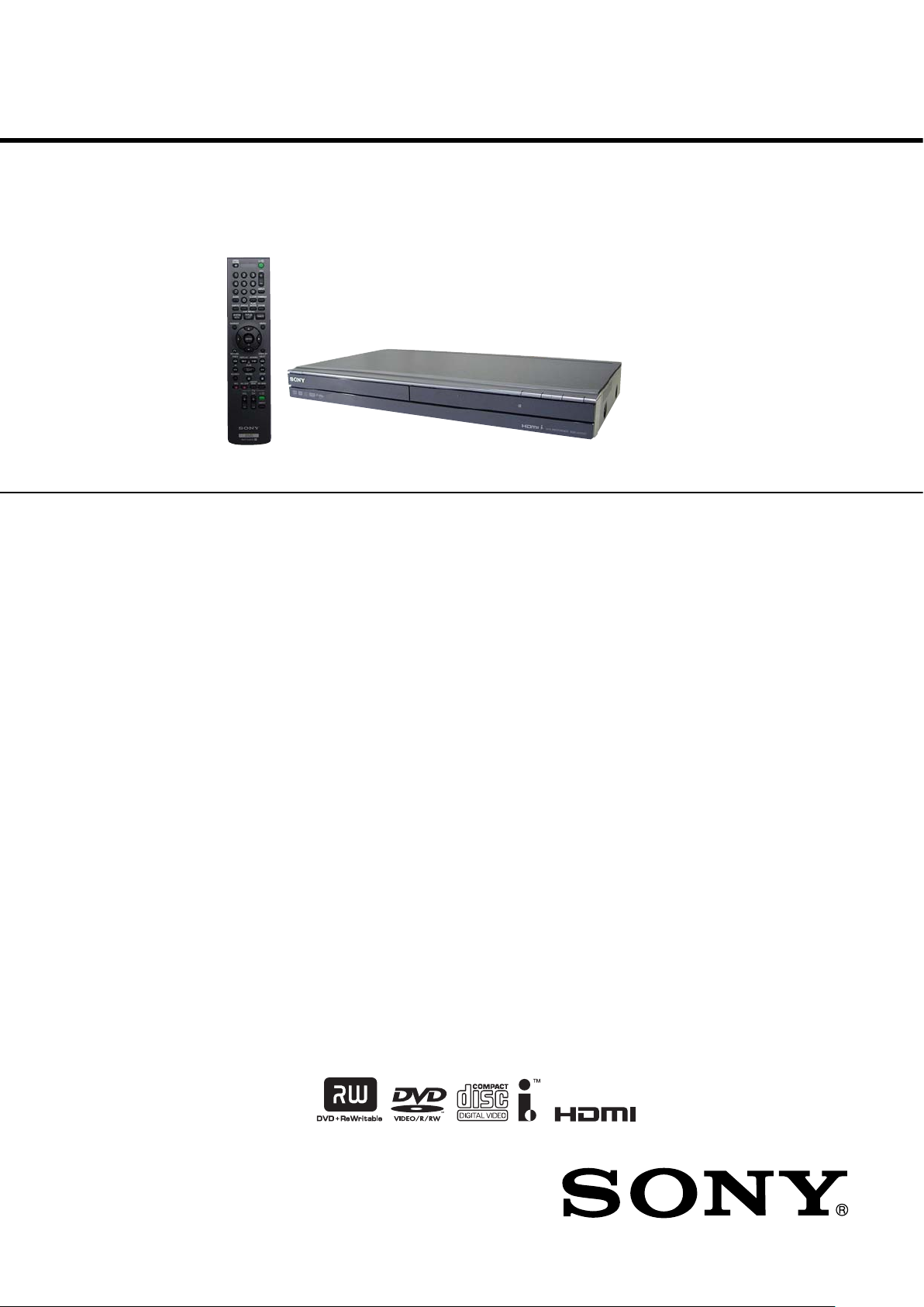
RDR-GX257/GX380
System
Laser: Semiconductor laser
Channel coverage:
NTSC
(Canadian, E)
VHF: 2 to 13
UHF: 14 to 69
CATV: A8 to A1, A to W, W+1 to
W+84
(AEP, UK, Russian)
The above channel coverage merely ensures the
channel reception within these ranges. It does not
guarantee the ability to receive signals in all
circumstances. The channels that can be received
differ depending on the country/region.
Video reception (GX380): Frequency
synthesizer system
Audio reception (GX380): Split carrier system
Antenna out (GX380): 75-ohm asymmetrical
antenna socket
Timer: Clock: Quartz locked/Timer
indication: 12-hour cycle (digital)
Video recording format: MPEG-2
Audio recording format/applicable bit
rate: Dolby Digital 2 ch
256 kbps (in HQ and SP mode), 192 kbps
(in LP and EP mode), 96 kbps (in ULP
mode)
Inputs and outputs
LINE 1 IN (US, Canadian, E, Australian, Singapore)
(VIDEO): Phono jack /1.0 Vp-p
(AUDIO): Phono jack (2)/2 Vrms/47 kilohms
LINE OUT (US, Canadian, E, Australian, Singapore)
(VIDEO): Phono jack /1.0 Vp-p
(AUDIO): Phono jack (2 each)/2 Vrms/600
ohms
LINE 2 IN
(VIDEO): Phono jack/1.0 Vp-p
(AUDIO): Phono jack/2 Vrms/more than
47 kilohms
Phono jack/2 Vrms/600 ohms
DV IN: 4-pin/i.LINK S100
DIGITAL OUT (COAXIAL): Phono jack/
0.5 Vp-p/75 ohms
COMPONENT VIDEO OUT
(Y, P
B, PR) (US, Canadian E):
Phono jack/Y: 1.0 Vp-p,
P
B: 0.7 Vp-p, PR: 0.7 Vp-p
HDMI OUT: HDMI™ Connector
USB: USB jack Type A
General
Power requirements:
Power consumption: 20 W
Dimensions (approx.):
430
120 V AC, 60 Hz (US, Canadian)
220 − 240 V AC, 50/60 Hz
(AEP, UK, Australian, Russian, Singapore)
110 − 240 V AC, 50/60 Hz (E)
× 53 × 258 mm (width/height/depth)
incl. projecting parts
Mass (approx.): 2.6 kg
Operating temperature: 5ºC to 35ºC
Operating humidity: 25% to 80%
Supplied accessories:
Power cord (1)
Antenna cable (1) (GX380)
Audio cord (1)
(US, Canadian, E, Australian, Singapore)
Video cord (1)
(US, Canadian, E, Australian, Singapore)
Remote commander (remote) (1)
Size AA (R6) batteries (2)
Set top box controller (1) (GX257)
Plug adapter (1) (E)
Specifications and design are subject to change
without notice.
PAL (B/G, D/K,I)/SECAM(L)
VHF: E2 to E12, R1 to R12, F2 to F10,
Italian AtoH, Ireland A toJ,South Africa
4 to 11, 13
UHF:E21to E69,R21 toR69, B21 toB69,
F21 to F69
CATV: S01to S05, S1 to S20, FranceB to
Q
HYPER: S21 to S41
AUDIO OUT (US, AEP, UK, E, Russian):
LINE 1-TV (AEP, UK, Russian): 21-pin
CVBS IN/OUT
RGB OUT (upstream)
LINE 3/DECODER (AEP, UK, Russian): 21-pin
CVBS IN/OUT
S-Video/RGB IN
Decoder
(Australian, Singapore)
PAL/SECAM (B/G, D/K, I)
VHF: E2to E12,R1 toR12, ItalianAto H,
Ireland A to J, SouthAfrica 4 to 11, 13,
AS0 to AS12, NZ1toNZ11
UHF:E21 to E69,R21 toR69, B21 toB69,
AS28 to AS69
CATV: S01 toS05, S1to S20
HYPER: S21 to S41
(Y, P
Russian, Singapore):
B/CB, PR/CR) (AEP, UK, Australian,
Phono jack/Y: 1.0 Vp-p,
P
B/CB: 0.7 Vp-p, PR/CR: 0.7 Vp-p
RMT-D256P/D257A
SERVICE MANUAL
Ver. 1.0 2008.07
Photo: RDR-GX257
SPECIFICATIONS
US Model
RDR-GX257
Canadian Model
AEP Model
UK Model
E Model
Australian Model
Russian Model
Singapore Model
RDR-GX380
9-883-990-11
Sony Corporation
Video Business Group
DVD RECORDER
Published by Quality Assurance Dept.
2008G0500-1
© 2008.7
SAFETY CHECK-OUT
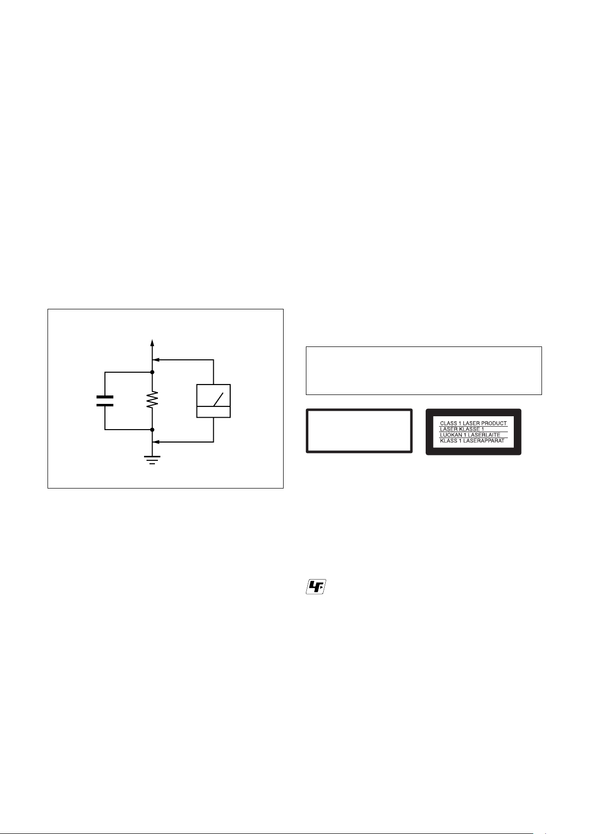
1.5 k0.15 µF
AC
voltmeter
(0.75 V)
To Exposed Metal
Parts on Set
Earth Ground
This appliance is classified as a
CLASS 1 LASER product. The
CLASS 1 LASER PRODUCT
MARKINGis locatedon therear ofthe
unit. (AEP, UK, Russian)
This label is located on the laser
protective housing inside the
enclosure.
CAUTION
CLASS 3BVISIBLE AND INVISIBLE LASER RADIATION WHEN OPEN.
AVOID EXPOSURETO THE BEAM.
UNDGÅ UDSAETTELSE FOR STRÅLING.
KLASSE 3B SYNLIG OG USYNLIG LASERSTRÅLINGVED ÅBNING.
UNNGÅ EKSPONERING FOR STRÅLEN.
KLASSE 3B
SYNLIG
OG USYNLIG
LASERSTRÅLING NÅR DEKSEL ÅPENS.
KLASS 3B SYNLIG OCH OSYNLIG LASERSTRÅLNING NÄR DENNA DEL ÄR
ÖPPNAD. STRÅLEN ÄR FARLIG.
AVATTAESSA OLET ALTTIINA LUOKAN 3B NÄKYVÄÄJA NÄKYMÄTÖNT
Ä
LASERSÄTEILYLLEVARO ALTISTUMISTA SÄTEELLE.
ADVARSEL
ADVARSEL
VARNING
VARO
SICHTBARE UND UNSICHTBARE LASERSTRAHLUNG KLASSE 3B,WENN
ABDECKUNG GE
Ö
FFNET. NICHT DEM STRAHL AUSSETZEN.
VORSICHT
After correcting the original service problem, perform the following
safety checks before releasing the set to the customer:
RDR-GX257/GX380
1. Check the area of your repair for unsoldered or poorly-soldered
connections. Check the entire board surface for solder splashes
and bridges.
2. Check the interboard wiring to ensure that no wires are “pinched”
or contact high-wattage resistors.
3. Look for unauthorized replacement parts, particularly transistors,
that were installed during a previous repair. Point them out to
the customer and recommend their replacement.
4. Look for parts which, though functioning, show obvious signs
of deterioration. Point them out to the customer and recommend
their replacement.
5. Check the line cord for cracks and abrasion. Recommend the
replacement of any such line cord to the customer.
6. Check the B+ voltage to see it is at the values specified.
7. Check the antenna terminals, metal trim, “metallized” knobs,
screws, and all other exposed metal parts for AC leakage. Check
leakage as described below.
LEAKAGE TEST
The AC leakage from any exposed metal part to earth ground and
from all exposed metal parts to any exposed metal part having a
return to chassis, must not exceed 0.5 mA (500 microamperes).
Leakage current can be measured by any one of three methods.
1. A commercial leakage tester, such as the Simpson 229 or RCA
WT-540A. Follow the manufacturers' instructions to use these
instruments.
2. A battery-operated AC milliammeter. The Data Precision 245
digital multimeter is suitable for this job.
3. Measuring the voltage drop across a resistor by means of a
VOM or battery-operated AC voltmeter. The “limit” indication
is 0.75V, so analog meters must have an accurate low-voltage
scale. The Simpson 250 and Sanwa SH-63Trd are examples
of a passive VOM that is suitable. Nearly all battery operated
digital multimeters that have a 2V AC range are suitable. (See
Fig. A)
CAUTION:
The use of optical instrument with this product will increase eye
hazard.
CAUTION
Use of controls or adjustments or performance of procedures
other than those specified herein may result in hazardous radiation exposure.
Fig. A. Using an AC voltmeter to check AC leakage.
WHEN SERVICING, DO NOT APPROACH THE LASER
EXIT WITH THE EYE TOO CLOSELY. IN CASE IT IS
NECESSARY TO CONFIRM LASER BEAM EMISSION,
BE SURE TO OBSERVE FROM A DISTANCE OF MORE
THAN 25 cm FROM THE SURFACE OF THE OBJECTIVE LENS ON THE OPTICAL PICK-UP BLOCK.
SAFETY-RELATED COMPONENT WARNING!!
COMPONENTS IDENTIFIED BY MARK 0 OR DOTTED LINE
WITH MARK 0 ON THE SCHEMATIC DIAGRAMS AND IN
THE PARTS LIST ARE CRITICAL TO SAFE OPERATION. REPLACE THESE COMPONENTS WITH SONY PARTS WHOSE
PART NUMBERS APPEAR AS SHOWN IN THIS MANUAL OR
IN SUPPLEMENTS PUBLISHED BY SONY.
ATTENTION AU COMPOSANT AYANT RAPPORT
LES COMPOSANTS IDENTIFIÉS PAR UNE MARQUE 0
SUR LES DIAGRAMMES SCHÉMATIQUES ET LA LISTE
DES PIÈCES SONT CRITIQUES POUR LA SÉCURITÉ DE
FONCTIONNEMENT. NE REMPLACER CES COM- POSANTS
QUE PAR DES PIÈCES SONY DONT LES NUMÉROS SONT
DONNÉS DANS CE MANUEL OU DANS LES SUPPLÉMENTS PUBLIÉS PAR SONY.
WARNING!!
À LA SÉCURITÉ!
Unleaded solder
Boards requiring use of unleaded solder are printed with the leadfree mark (LF) indicating the solder contains no lead.
(Caution: Some printed circuit boards may not come printed with
the lead free mark due to their particular size.)
: LEAD FREE MARK
Unleaded solder has the following characteristics.
• Unleaded solder melts at a temperature about 40°C higher than
ordinary solder.
Ordinary soldering irons can be used but the iron tip has to be
applied to the solder joint for a slightly longer time.
Soldering irons using a temperature regulator should be set to
about 350°C.
Caution: The printed pattern (copper foil) may peel away if the
heated tip is applied for too long, so be careful!
• Strong viscosity
Unleaded solder is more viscous (sticky, less prone to flow) than
ordinary solder so use caution not to let solder bridges occur such
as on IC pins, etc.
• Usable with ordinary solder
It is best to use only unleaded solder but unleaded solder may
also be added to ordinary solder.
– 2 –

RDR-GX257/GX380
TABLE OF CONTENTS
Section Title Page Section Title Page
1. SERVICE NOTE
1-1. EEPROM IC Setting ..................................................... 1-1
1-2. Disc Removal Procedure If The Tray Cannot Be
Ejected (Forced Ejection) ............................................. 1-2
1-3. How To Distinguish Difference Of AEP Model .............. 1-2
2. DISASSEMBLY
2-1. Disassembly Flow ........................................................ 2-1
2-2. Top Case ...................................................................... 2-1
2-3. Front Panel ................................................................... 2-2
2-4. Mechanism Deck .......................................................... 2-2
2-5. IO Board ....................................................................... 2-3
2-6. Circuit Boards Location ................................................ 2-3
3. BLOCK DIAGRAMS
3-1. Overall Block Diagram
(US, Canadian, E, Australian, Singapore) .................... 3-1
3-2. Overall Block Diagram (AEP, UK, Russian) ................. 3-2
3-3. Power Block Diagram ................................................... 3-3
4. SCHEMATIC DIAGRAMS
4-1. Frame Schematic Diagram (1/2) .................................. 4-1
4-2. Frame Schematic Diagram (2/2) .................................. 4-2
4-3. IO Board (SMPS) Schematic Diagram (1/4)................. 4-3
4-4. IO Board (MICOM/TUNER)
Schematic Diagram (2/4).............................................. 4-4
4-5. IO Board (CONNECTOR/AV SWITCH/JACK)
Schematic Diagram (3/4).............................................. 4-5
4-6. IO Board (V DECODER/A.DAC/MIC INPUT)
Schematic Diagram (4/4).............................................. 4-6
4-7. MAIN Board (MPEG) Schematic Diagram (1/5) ........... 4-7
4-8. MAIN Board (DDR/LATCH/FLASH/RESET)
Schematic Diagram (2/5).............................................. 4-8
4-9. MAIN Board (DV1394/INTERFACE CONNECTOR)
Schematic Diagram (3/5).............................................. 4-9
4-10. MAIN Board (RF/MOTOR DRIVE)
Schematic Diagram (4/5).............................................. 4-10
4-11. MAIN Board (DSP) Schematic Diagram (5/5) .............. 4-11
4-12. HDMI Board (HDMI CONNECTOR)
Schematic Diagram ...................................................... 4-12
4-13. TIMER Board (FL DRIVER)
Schematic Diagram (1/2).............................................. 4-13
4-14. TIMER Board (AV INPUT/USB INPUT/DV1394 INPUT)
Schematic Diagram (2/2).............................................. 4-14
4-15. KEY Board (POWER SWITCH) Schematic Diagram ... 4-15
4-16. Waveforms ................................................................... 4-16
4-17. Circuit Voltage Chart .................................................... 4-24
5. PRINTED WIRING BOARDS
5-1. IO Board (IO/SMPS) Printed Wiring Board
(Component Side) ........................................................ 5-1
5-2. IO Board (IO/SMPS) Printed Wiring Board
(Conductor Side) .......................................................... 5-2
5-3. MAIN Board (MAIN/LOADER) Printed Wiring Board
(Component Side) ........................................................ 5-3
5-4. MAIN Board (MAIN/LOADER) Printed Wiring Board
(Conductor Side) .......................................................... 5-4
5-5. HDMI Board (HDMI CONNECTOR)
Printed Wiring Board .................................................... 5-5
5-6. TIMER Board (FRONT) Printed Wiring Board.............. 5-6
5-7. KEY Board (POWER SWITCH)
Printed Wiring Board .................................................... 5-7
6. TROUBLESHOOTING ............................................. 6-1
7. REPAIR PARTS LIST
7-1. Exploded Views ............................................................ 7-1
7-1-1. Case Section ........................................................... 7-1
7-1-2. Mechanism Deck Section ........................................ 7-2
7-1-3. Accessories ............................................................. 7-3
7-2. Electrical Parts List ....................................................... 7-4
– 3 –
RDR-GX257/GX380
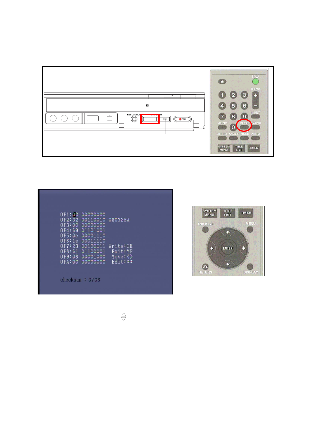
1. Press the CLEAR buttton on the remocom together with “ Program ŷ ” on the front panel about 㫧 6 sec.
The picture on OSD will be as bellow :
Model : RDR-GX380 / RDR-GX257
2. To MOVE from OP1 (Option 1) to another option, Press “Ż Ź “ button on the remote control or front panel.
3. To CHANGE the option code, press “ “on the remote control.
4. To APPLY the option code, after change the option press “OK/ENTER” button on the remote control.
5. To INITIALIZE the system, press “CLEAR” button on the remote control and “Program ŷ ” on the front panel
together about ± 6 sec.
6. To exit from the option code menu without initializing the system, just turn off the power and then turn on again.
䂥
䂯
SECTION 1
SERVICE NOTE
1-1. EEPROM IC SETTING
1-1
RDR-GX257/GX380
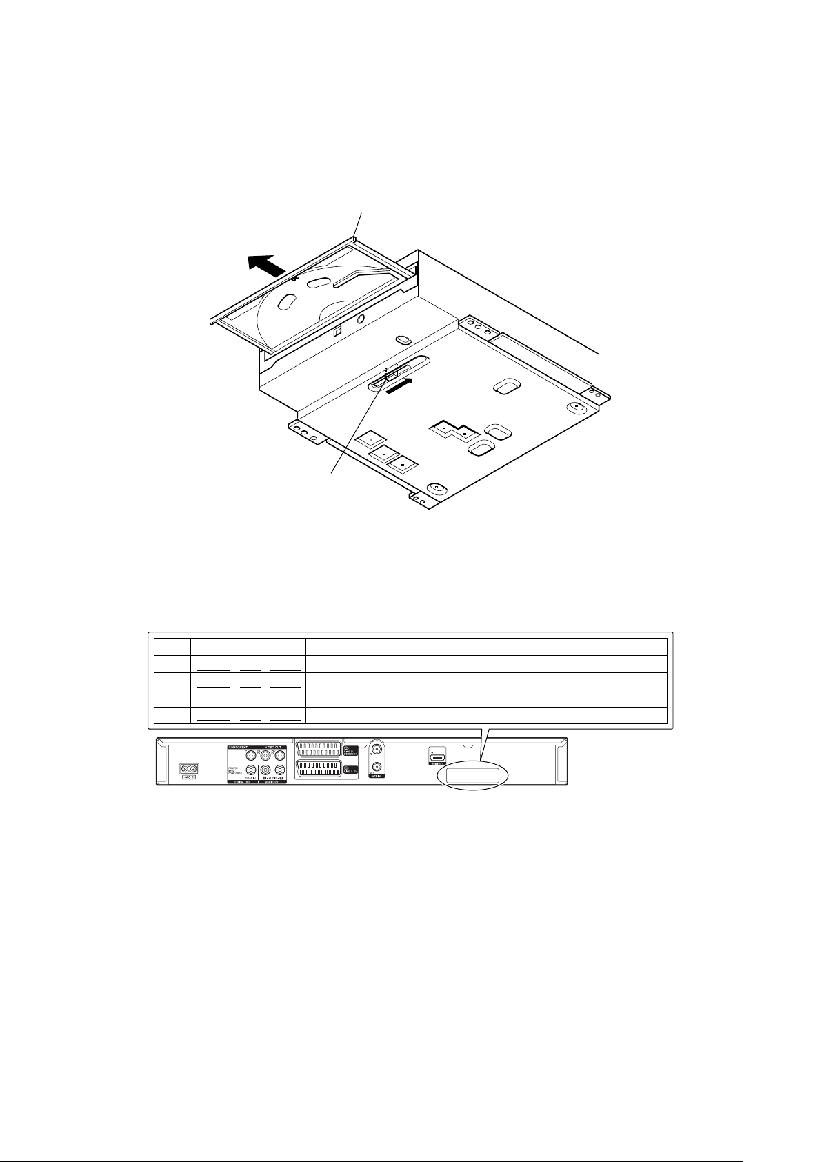
Tray
Lever
Serial No.
GX380 EC1 XXXX
GX380 EC2 XXXX
GX380 EC3 XXXX
AEP1
AEP2
AEP3
Area
Germany,Italy, Switzerland, Austria, Spain,Israel, Netherlands, Belgium
Sweden, Denmark, Finland, Norway, Portugal, Greece,Turkey, Poland,
Czech Republic, Slovakia, Hungary, Slovene, Croatia, Cypriot
France, Switzerland
1-2. DISC REMOVAL PROCEDURE IF THE TRAY CANNOT BE EJECTED (FORCED EJECTION)
1. Remove the top case. (Refer to page 2-1)
2. Remove the front panel and the mechanism deck. (Refer to page 2-2)
3. Slide the lever of bottom of mechanism deck and open the tray.
1-3. HOW TO DISTINGUISH DIFFERENCE OF AEP MODEL
1-2E
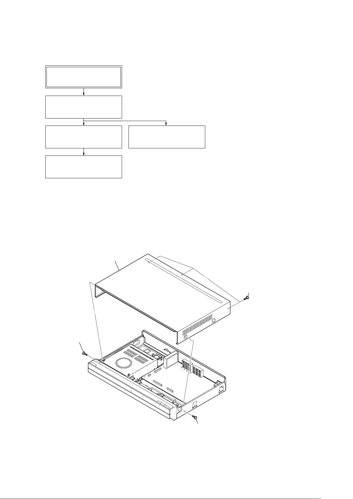
• This set can be disassembled in the order shown below.
2-2. TOP CASE
(Page 2-1)
2-3. FRONT PANEL
(Page 2-2)
2-4. MECHANISM DECK
(Page 2-2)
2-5. IO BOARD
(Page 2-3)
SET
1 Screw
2 Screw
3 Three screws
4 Top case
2-1. DISASSEMBLY FLOW
RDR-GX257/GX380
SECTION 2
DISASSEMBLY
Note 2: Follow the disassembly procedure in the numerical order given.
2-2. TOP CASE
2-1
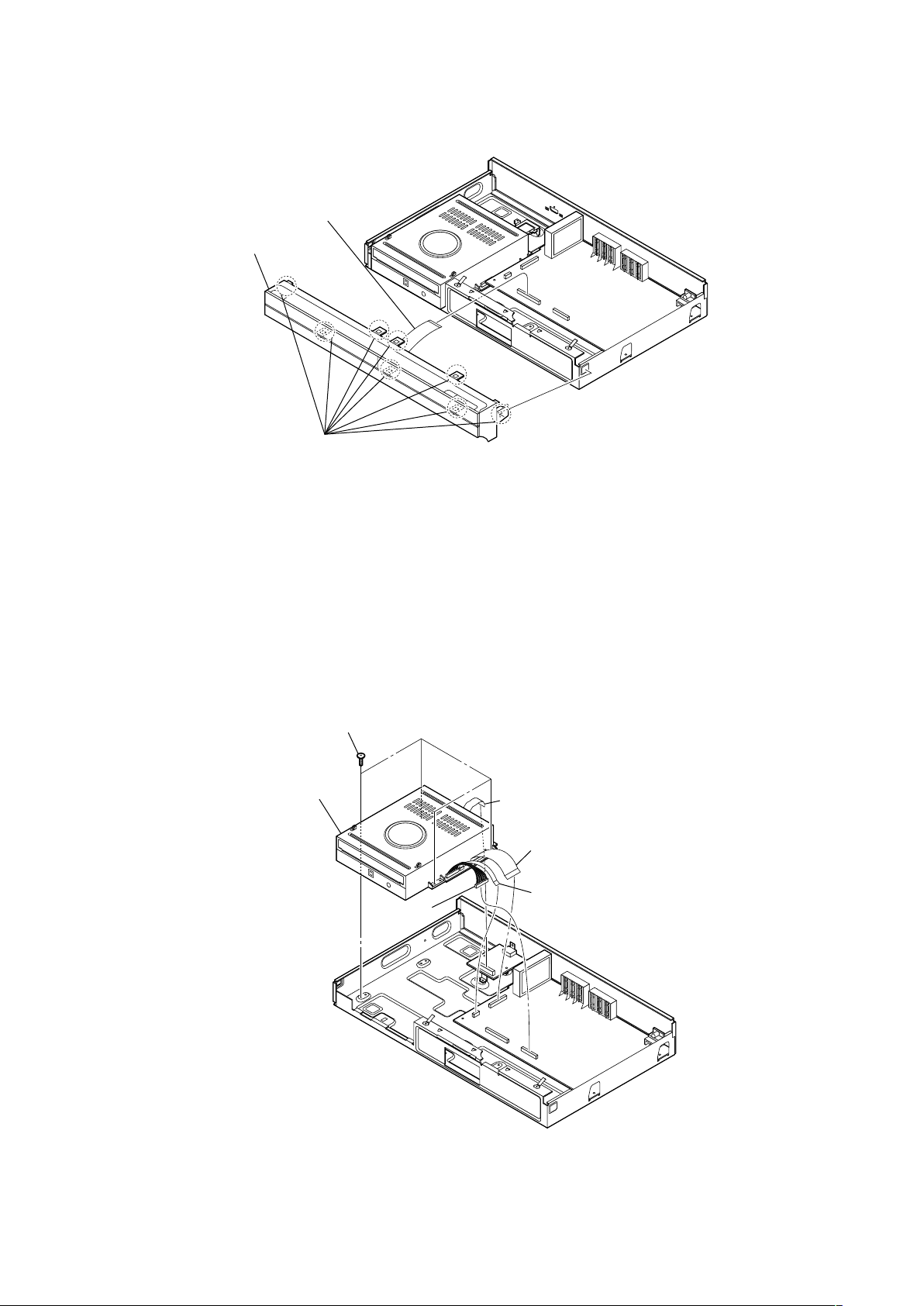
2-3. FRONT PANEL
1 Flexible flat cable (TI-1)
2 Eight claws
3 Front panel
3 Flexible flat cable (MI-1)
4 Flexible flat cable (MH-1)
1 Harness
2 Flexible flat cable (MI-2)
5 Four screws
6 Mechanism deck
RDR-GX257/GX380
2-4. MECHANISM DECK
2-2
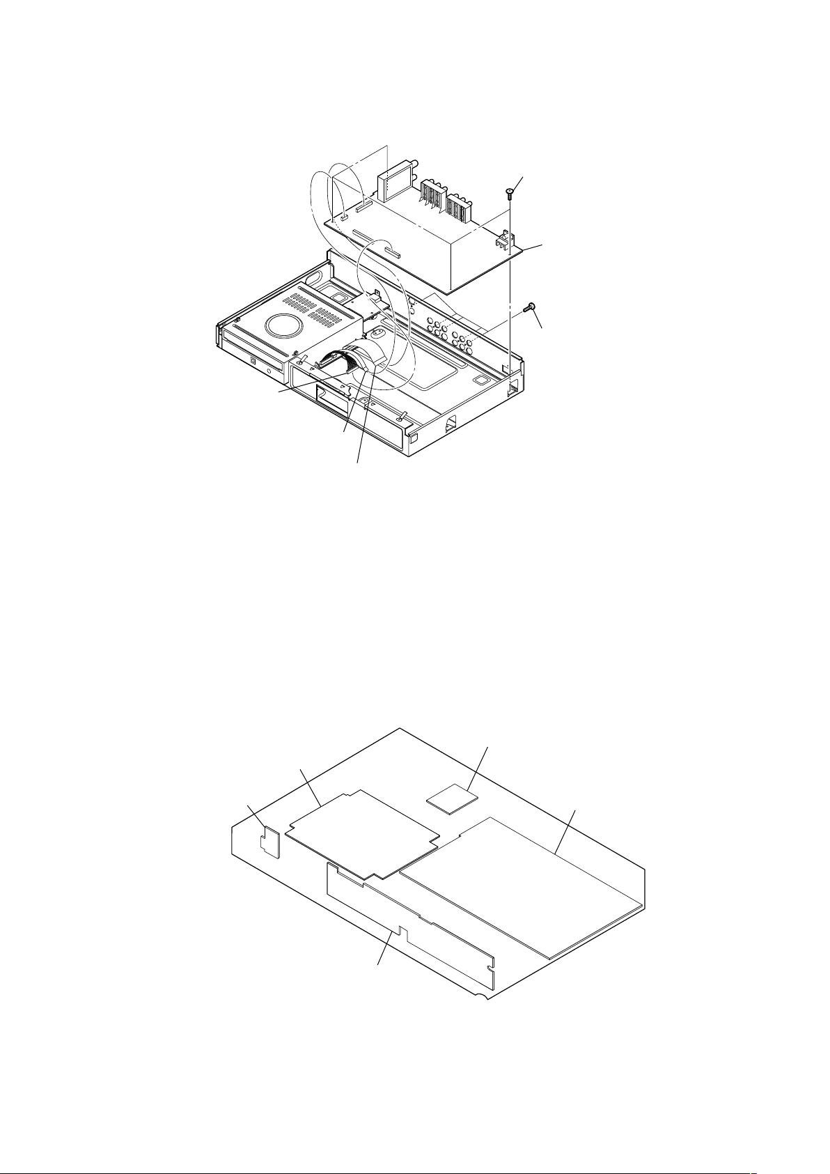
2-5. IO BOARD
3 Flexible flat cable (MI-1)
6 IO board
1 Harness
2 Flexible flat cable (MI-2)
4 Five screws
5 Four screws
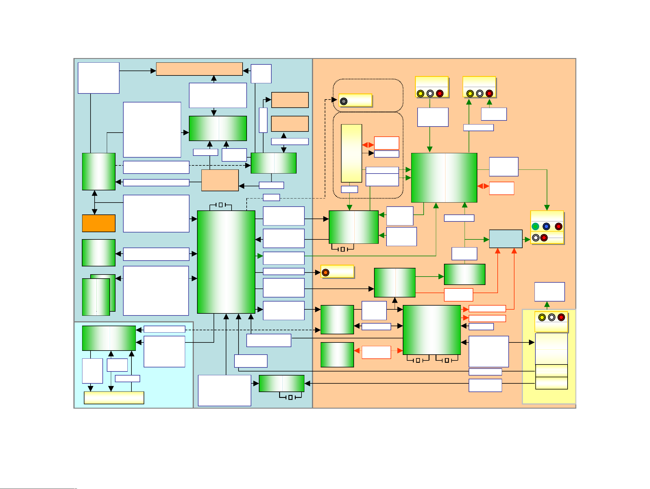
KEY board
MAIN board
TIMER board
IO board
HDMI board
RDR-GX257/GX380
2-6. CIRCUIT BOARDS LOCATION
2-3E
3-1
RDR-GX257/GX380
FLD
DRIVER
24.576MHz
EU1_V_IN
EU1_A_IN_L
EU1_A_IN_R
SIF
TU_A_L
TU_A_R
TU_V_OUT
I2C_CLK
I2C_DATA
Z_MUTE_L
Z_MUTE_R
A_MUTE_L
YPbPr_Mute_L
DMN8603
MPEG
DVD_CVBS,G/Y
DVD_B/Pb,R/Pr
VI_CLK,D[0:7]
AI_D0,SCLK
AI_FSYNC
/VDEC_RST
AI_MCLK
SCL,SDA
FLASH
/FLASH_CS,OE,WE
BA[1:22], HD[0:15]
PHY
USB
E5_SDRAM_DQS[0:3]
E5_SDRAM_DQM[0:3]
/E5_SDRAM_WE,CAS,RAS
E5_SDRAM_CKE
E5_SDRAM_CLK[0:1]
/E5_SDRAM_CLK[0:1]
E5_SDRAM_DQ[0:31]
E5_SDRAM_A[0:15]
DDR
RF IC
AN22117A
ATAPI
(For TEST)
LPM101 (PICKUP)
DSP
BSMD,NBSMD
PKMD,NPKMD
PK2MD,NPK2MD
PK3MD,NPK3MD
LDD_ENABLE
GASW,A,B,C,D,E,F,G,H
RF+,RH-,TEMP,RESET
W1SET,W2SET,W3SET
/S_CD,VREFPD,FPD
LPF303
MD Front
F-DRV,T-DRV,TILT-DRV
L-DRV,SPIN, SFG,PRTFLG
/EJECT_KEY,/LOADSW
/OPENSW
LOAD+/-
WBL,WBLDIF,
BQOUTN,BQOUTP
CLUMPGT,LPPS,LPPN
RSDAT,RSEN
SDAT,SCK,SEN,
CH_SEL,TGCHG
LSEN,LSCLK,LSDAT
SH[1:6],WTGT,BD0
OFTR,TC,SE01,SE02
TILT+/TRK+/FCS+/-
LPM302
SLED MOTOR
LPM301
SPINDLE
LRPM
PRTRST
V,W,U,COM
AA+
BB+
ATA1_DMARQ,DMAACK
ATA1_WR,RD,IORDY
ATA1_INTRQ
/ATA1_CS[0:1]
NDASP,NPDIAG
ATA1_D[0:15],ADD[0:2]
DV IN
HOST_ENA_L
HOST_CLK_IN
HOST_DATA_IN
Front AV
F_A_L_IN
F_A_R_IN
F_VIDEO_IN
IO
MAIN
USB_BDM0
USB_BDP0
BIO_PHY_DATA[0:7]
BIO_PHY_CTL[0:1]
BIO_CLK,LPS
LINK_ON, /PHY_RST
SCL,SDA
AO_MCLK
AO_D0,SCLK
AO_FSYNC
V.ENC
A.DSP
SAA7138
IC901
T
U
N
E
R
SW_A_L
SW_A_R
SW_CVBS
AV Switch
V.Buffer
MM1763
IC801
I2C_CLK
I2C_DATA
SPI_CS,
SPI_CLK
SPI_MOSI
OPAMP
DAC
SPDIF
Coax
G_Y_OUT
B_Pb_OUT
R_Pr_OUT
A_OUT_L
A_OUT_R
IC701
MICOM
AUDIO
MUTE
F_A_L_IN
F_A_R_IN
F_VIDEO_IN
TIMER
HDMI
10MHz
32.768KHz
CEC_TX,RX
I2C_CLK
I2C_DATA
EEPROM
VO_CLK,D[0:15]
AO_MCLK
SPDIF
/HDMI_RST
SCL,SDA
CEC
24.576MHz
IC1601
IC1101
LIC101
MOTOR DRIVE
BD7776
LIC301
LIC201
IC1301
IC1201
IC1202
PCM1780
IC911
S4580
IC910
Buffer
74HCT125
IC702
24CS16
IC703
AV OUTAV IN
EU1_V_OUT
Y Pb Pr
L/R
EU1_V_OUT
A_OUT_L
A_OUT_R
REAR AV IN/OUT
13.5MHz
DMN8603
MPEG
IC1101
IR Tx
Tuner option
Tunerless option
AFT
AFT
USB_D+/TPA+/-
TPB+/-
RMC_IN
FLD_CLK
FLD_ENA_L
FLD_DATA_OUT
KEY_RTN_[0:1]
HDMI TX
HDMI JACK
IC1701
TX0+/TX1+/TX2+/TXC+/-
HP_DET
DSCL
DSDA
HOST_DATA_OUT
/DVD_RST
IR
SECTION 3
BLOCK DIAGRAMS
3-1. OVERALL BLOCK DIAGRAM (US, Canadian, E, Australian, Singapore)
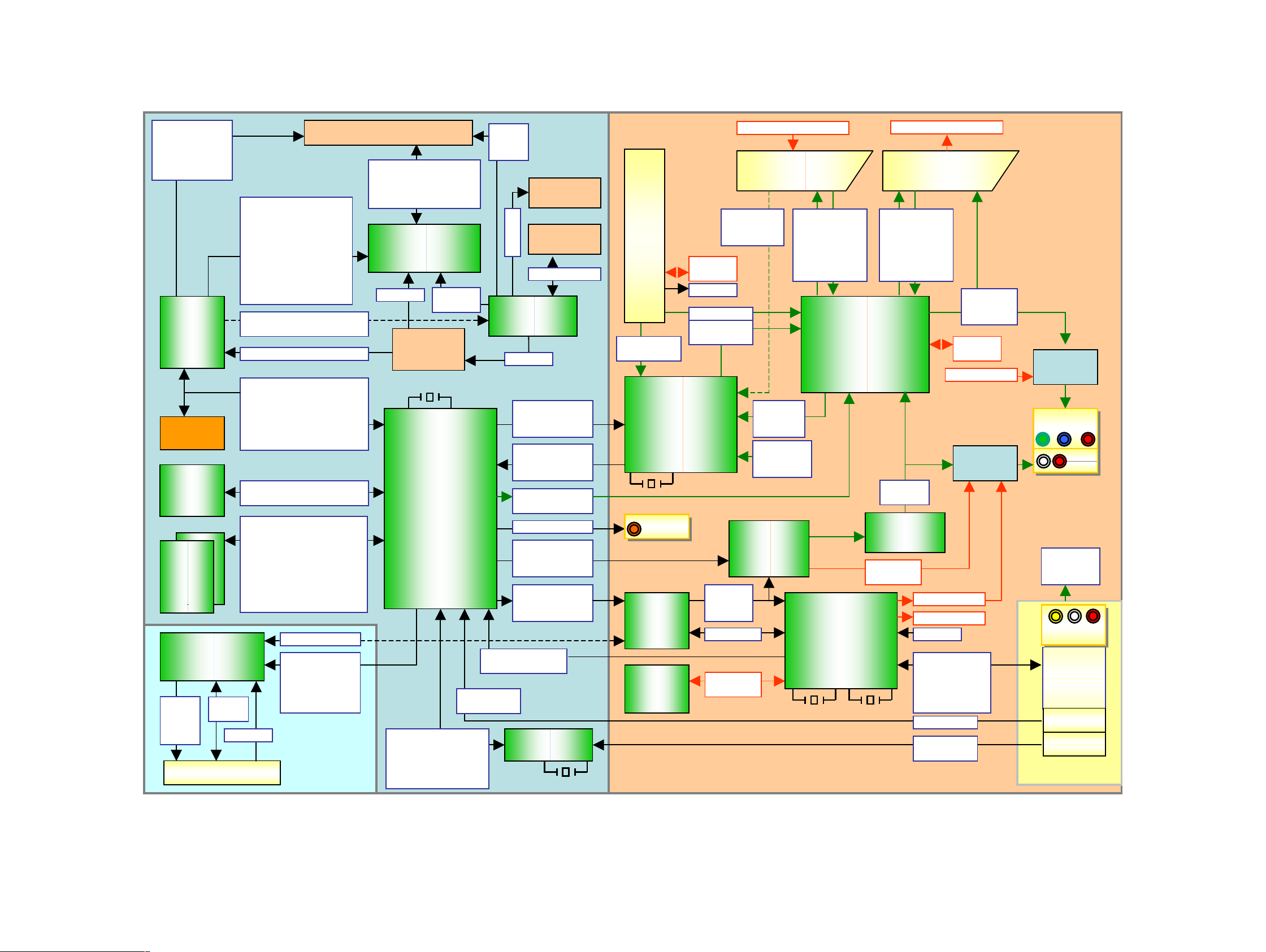
3-2
RDR-GX257/GX380
SCART 1
(TV)
SCART 2
(Decorder)
FLD
DRIVER
24.576MHz
EU2_V_OUT
EU2_A_OUT_L
EU2_A_OUT_R
EU2_V_IN
EU2_A_IN_L
EU2_A_IN_R
EU1_V_OUT
EU1_A_OUT_L
EU1_A_OUT_R
EU1_V_IN
EU1_A_IN_L
EU1_A_IN_R
R_SCART_IN
G_SCART_IN
B_SCART_IN
Y/Pb/Pr
MUTE
SIF
SECAM_AM
TU_A_L
TU_A_R
TU_V_OUT
I2C_CLK
I2C_DATA
YPbPr_Mute_L
Z_MUTE_L
Z_MUTE_R
A_MUTE_L
YPbPr_Mute_L
RGB_IN, C+_DET_H
RGB_OUT_H,SCART_H
DMN8603
MPEG
13.5MHz
DVD_CVBS,G/Y
DVD_B/Pb,R/Pr
VI_CLK,D[0:7]
AI_D0,SCLK
AI_FSYNC
/VDEC_RST
AI_MCLK
SCL,SDA
FLASH
/FLASH_CS,OE,WE
BA[1:22], HD[0:15]
PHY
USB
E5_SDRAM_DQS[0:3]
E5_SDRAM_DQM[0:3]
/E5_SDRAM_WE,CAS,RAS
E5_SDRAM_CKE
E5_SDRAM_CLK[0:1]
/E5_SDRAM_CLK[0:1]
E5_SDRAM_DQ[0:31]
E5_SDRAM_A[0:15]
DDR
RF IC
AN22117A
ATAPI
(For TEST)
LPM101 (PICKUP)
DSP
BSMD,NBSMD
PKMD,NPKMD
PK2MD,NPK2MD
PK3MD,NPK3MD
LDD_ENABLE
GASW,A,B,C,D,E,F,G,H
RF+,RH-,TEMP,RESET
W1SET,W2SET,W3SET
/S_CD,VREFPD,FPD
LPF303
MD Front
F-DRV,T-DRV,TILT-DRV
L-DRV,SPIN, SFG,PRTFLG
/EJECT_KEY,/LOADSW
/OPENSW
LOAD+/-
WBL,WBLDIF,
BQOUTN,BQOUTP
CLUMPGT,LPPS,LPPN
RSDAT,RSEN
SDAT,SCK,SEN,
CH_SEL,TGCHG
LSEN,LSCLK,LSDAT
SH[1:6],WTGT,BD0
OFTR,TC,SE01,SE02
TILT+/TRK+/FCS+/-
LPM302
SLED MOTOR
LPM301
SPINDLE
LRPM
PRTRST
V,W,U,COM
AA+
BB+
ATA1_DMARQ,DMAACK
ATA1_WR,RD,IORDY
ATA1_INTRQ
/ATA1_CS[0:1]
NDASP,NPDIAG
ATA1_D[0:15],ADD[0:2]
DV IN
HOST_ENA_L
HOST_CLK_IN
HOST_DATA_IN
Front AV
F_A_L_IN
F_A_R_IN
F_VIDEO_IN
IO
MAIN
USB_D+/TPA+/-
TPB+/-
USB_BDM0
USB_BDP0
BIO_PHY_DATA[0:7]
BIO_PHY_CTL[0:1]
BIO_CLK,LPS
LINK_ON, /PHY_RST
SCL,SDA
AO_MCLK
AO_D0,SCLK
AO_FSYNC
V.ENC
A.DSP
SAA7138
IC901
T
U
N
E
R
SW_A_L
SW_A_R
SW_CVBS
AV Switch
V.Buffer
MM1763
IC801
I2C_CLK
I2C_DATA
Y Pb Pr
SPI_CS,
SPI_CLK
SPI_MOSI
RMC_IN
FLD_CLK
FLD_ENA_L
FLD_DATA_OUT
KEY_RTN_[0:1]
OPAMP
DAC
SPDIF
Coax
L/R
G_Y_OUT
B_Pb_OUT
R_Pr_OUT
A_OUT_L
A_OUT_R
IC701
MICOM
AUDIO
MUTE
F_A_L_IN
F_A_R_IN
F_VIDEO_IN
TIMER
HDMI
10MHz
32.768KHz
CEC_TX,RX
I2C_CLK
I2C_DATA
EEPROM
HDMI TX
VO_CLK,D[0:15]
AO_MCLK
SPDIF
/HDMI_RST
SCL,SDA
CEC
24.576MHz
IC1601
IC1101
LIC101
MOTOR DRIVE
BD7776
LIC301
LIC201
IC1301
IC1201
IC1202
PCM1780
IC911
S4580
IC910
Buffer
74HCT125
IC702
24CS16
IC703
HDMI JACK
AFT
AFT
IC1701
TX0+/TX1+/TX2+/TXC+/-
HP_DET
DSCL
DSDA
HOST_DATA_OUT
/DVD_RST
3-2. OVERALL BLOCK DIAGRAM (AEP, UK, Russian)
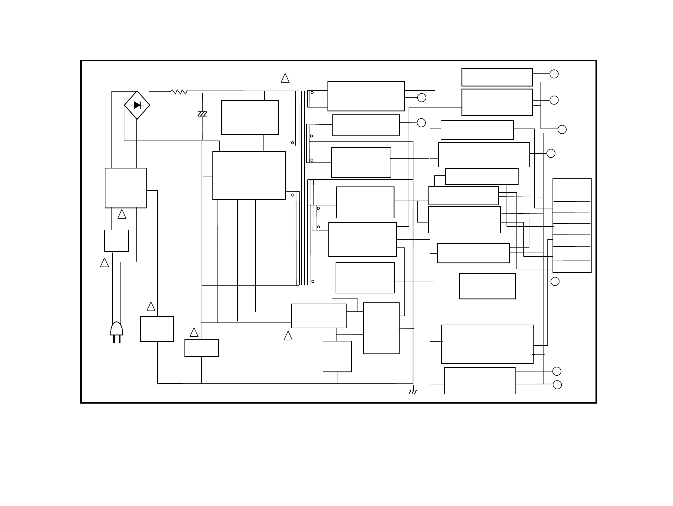
3-3E
RDR-GX257/GX380
FUSE
(F101)
NOISE FILTER
BLOCK
(C101,L102,
C102)
SNUBBER
BLOCK
(D101,C105
C106,R104)
DRIVE & S/W BLOCK
(IC101, D102, R105,
C104, C107, C108,C109,
R109, ZD101,ZD102)
PHOTO COUPLER
(IC102)
BD101
T101
TRANS
5V
1.25V
2.5V
R101
ԙ
Ԟ ԟ
Ԙ
ERROR
AMP
(IC103)
6
4
9
11
13
2
1
Ɣ
Y-CAP
C110
Y-CAP
C111
Ɣ
12
Ɣ
Ɣ
Ɣ
Ɣ
Ɣ
Ɣ
8
7
FEED-BACK
BLOCK
R121,R122,
C131,R123.
R124.R125
R126)
Ɣ
Ɣ
RECTIFIER &
SMOOTING BLOCK
(D121,D122,
C121,L121,C122)
RECTIFIER &
SMOOTING BLOCK
(D128,C130,
R138,ZD152)
3.3V
TO Main
(PVM03)
Ɣ
BR BL
(BK)(WH)
C103
Ɣ
14
15
12V REG & S/W BLOCK
(IC131,C133,R130)
5V REG & S/W BLOCK
(IC132,C134,R131)
Ɣ
!
!
!
!
!
!
Ɣ
Ԛ
Ɣ
Ɣ
Ɣ
ԛ
Ԝ
Ɣ
12V_Loader
RECTIFIER &
SMOOTING BLOCK
(D127,C126,C132,
R128,L123,C127)
RECTIFIER &
SMOOTING BLOCK
(D123,C123
,L122,C124)
RECTIFIER &
SMOOTING BLOCK
(D135,C129,R171)
RECTIFIER &
SMOOTING BLOCK
(D134,C120,R158
R160,R161, ZD151,R170)
10
2.5V REG & S/W BLOCK
(IC136,C140,R144
R146,C164)
3.3V REG & S/W BLOCK
(IC133,C137,R137,C142)
33V S/W Block
(Q167,R181,R182
R183,R184)
5V_I/O S/W Block
(Q168,R172,R173
D136,C163)
1.25V REG & S/W Block (DC-DC)
(IC151,R152,C158,C156,R153,
R154,R155,C157,L151,L152
C154,C152,R151,C159,R159
C155,C151,C153)
FD(-)
FD(+) S/W Block
(Q162,R168,R169,Q163)
S/W 5.3VA S/W Block
(Q161,R163,R164
R165,C162)
S/W FD(+)
-25VA
1W ‘H’
S/W 5.3VA
S/W 12VA
33V
Ɣ
Ɣ
P.CTL‘H’
Ɣ
Ɣ
Ɣ
Ɣ
Ɣ
Ɣ
S/W 12VA REG & S/W BLOCK
(Q164,R139,R140,R141,Q165,
Q166,C161,C160,ZD153)
5V_IO
1.8V
1.8V REG & S/W BLOCK
(IC134,C149,C138,C148)
Ɣ
Ɣ
TH01
3-3. POWER BLOCK DIAGRAM
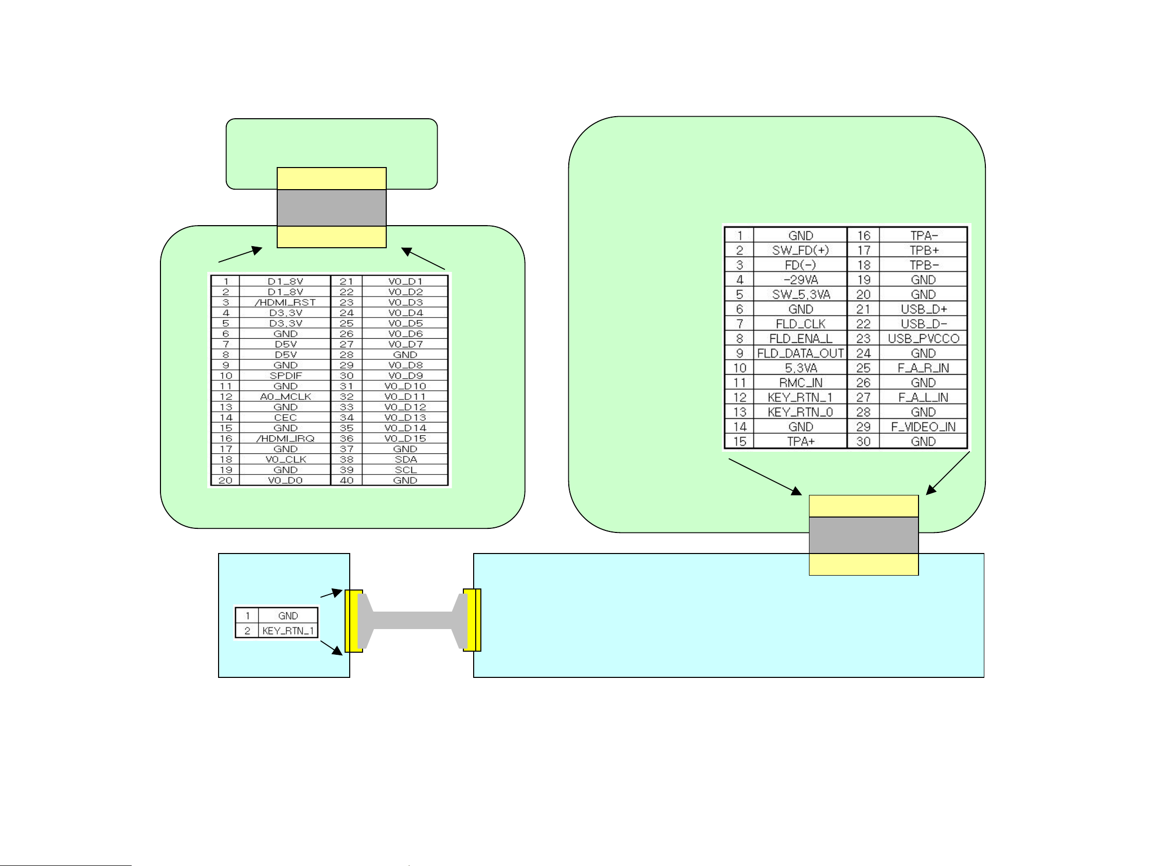
4-1
RDR-GX257/GX380
TIMRE BOARD
PTV01
PVT01
KEY BOARD
PMH01
PHM01
IO BOARD (1/2)
HDMI BOARD
MAIN BOARD (1/2)
PTT02
PTT01
4-1. FRAME SCHEMATIC DIAGRAM (1/2)
SECTION 4
SCHEMATIC DIAGRAMS

4-2
RDR-GX257/GX380
IO BOARD (2/2)MAIN BOARD (2/2)
PVM01
PMI01
PVM02
PMI02
PVM03
PMS01
4-2. FRAME SCHEMATIC DIAGRAM (2/2)
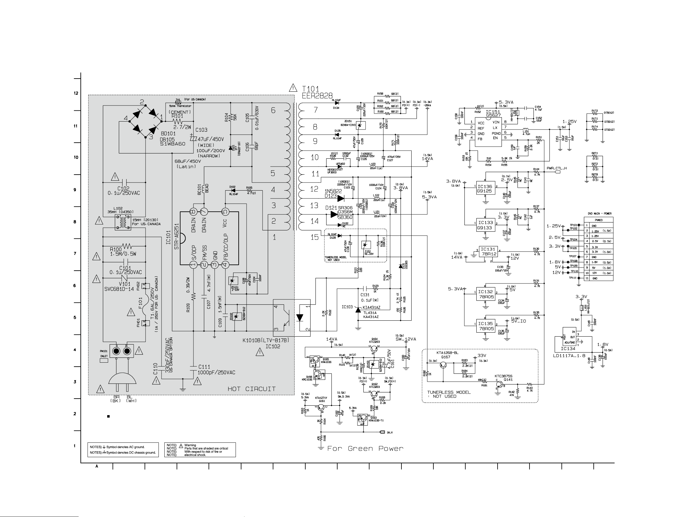
4-3
RDR-GX257/GX380
4-3. IO BOARD (SMPS) SCHEMATIC DIAGRAM (1/4) • See page 5-1 for printed wiring board.
A B C D E F G H I J K L M N O P Q
1. Shaded( ) partsare criticalfor safety.Replace only
withspecified partnumber.
2. Voltages areDC-measured witha digital voltmeterduring Playmode.
IMPORTANT SAFETY
NOTE :
WHEN SERVICING THIS CHASSIS, UNDER NO CIRCUMSTANCES SHOULD THE ORIGINALDESIGN BE
MODIFIED OR ALTERED WITHOUT PERMISSION
FROM THE SONY. ALLCOMPONENTS SHOULD
BEREPLACED ONLY WITH TYPES IDENTICAL TO
THOSE IN THE ORIGINALCIRCUIT. SPECIALCOMPONENTS ARE SHADED ON THE SCHEMATIC FOR
EASY IDENTIFICATION. THIS CIRCUIT DIAGRAM MAY
OCCASIONALLY DIFFER FROM THE ACTUALCIRCUITUSED. THIS WAY, IMPLEMENTATION OF THE
LATEST SAFETY AND PERFORMANCE IMPROVEMENT CHANGES INTO THE SETIS NOT DELAYED
UNTIL THE NEW SERVICE LITERATURE IS PRINTED.
IO BOARD (1/4)
SMPS
AC IN
4-4
RDR-GX257/GX380
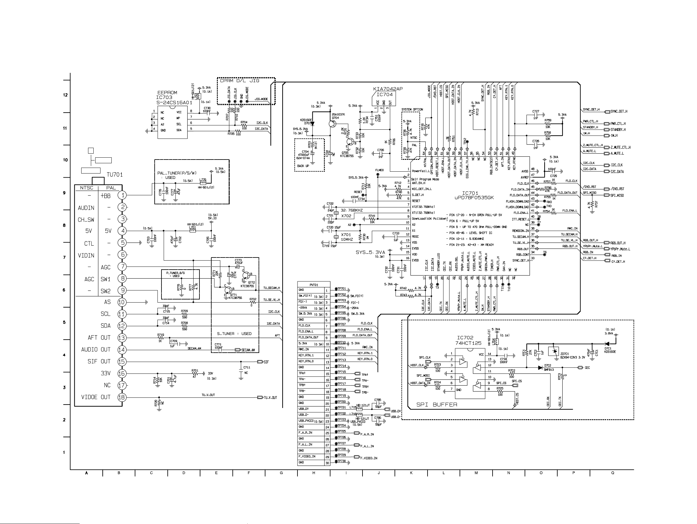
4-4. IO BOARD (MICOM/TUNER) SCHEMATIC DIAGRAM (2/4) • See page 5-1 for printed wiring board.
IO BOARD (2/4)
MICON/TUNER
ANTENNA
OUT (TO TV)
IN

4-5
RDR-GX257/GX380
4-5. IO BOARD (CONNECTOR/AV SWITCH/JACK) SCHEMATIC DIAGRAM (3/4) • See page 5-1 for printed wiring board.
IO BOARD (3/4)
CONNECTOR/AV SWITCH/JACK
OUTPUT
COMPONENT (Y/PB/PR)
DIGITALAUDIO (COAXIAL)/AUDIO(L/R)
IR TRANSMITTER
AV2(DECODER)
AV1
AEP,UK, Russian
INPUT1 (VIDEO/AUDIO (L/R))
OUTPUT (VIDEO/AUDIO (L/R))
US, Canadian, E,Australian, Singapore
4-6
RDR-GX257/GX380
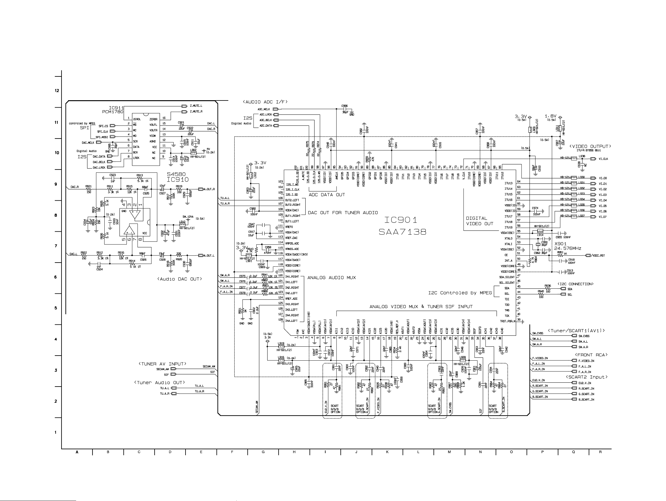
4-6. IO BOARD (V DECODER/A.DAC/MIC INPUT) SCHEMATIC DIAGRAM (4/4) • See page 5-1 for printed wiring board.
IO BOARD (4/4)
V DECODER/A.DAC/MICINPUT
4-7
RDR-GX257/GX380
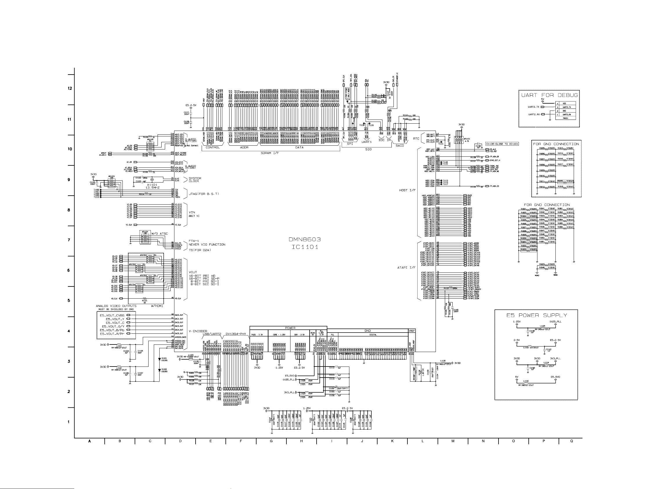
4-7. MAIN BOARD (MPEG) SCHEMATIC DIAGRAM (1/5) • See page 5-3 for printed wiring board.
MAIN BOARD (1/5)
MPEG
4-8
RDR-GX257/GX380
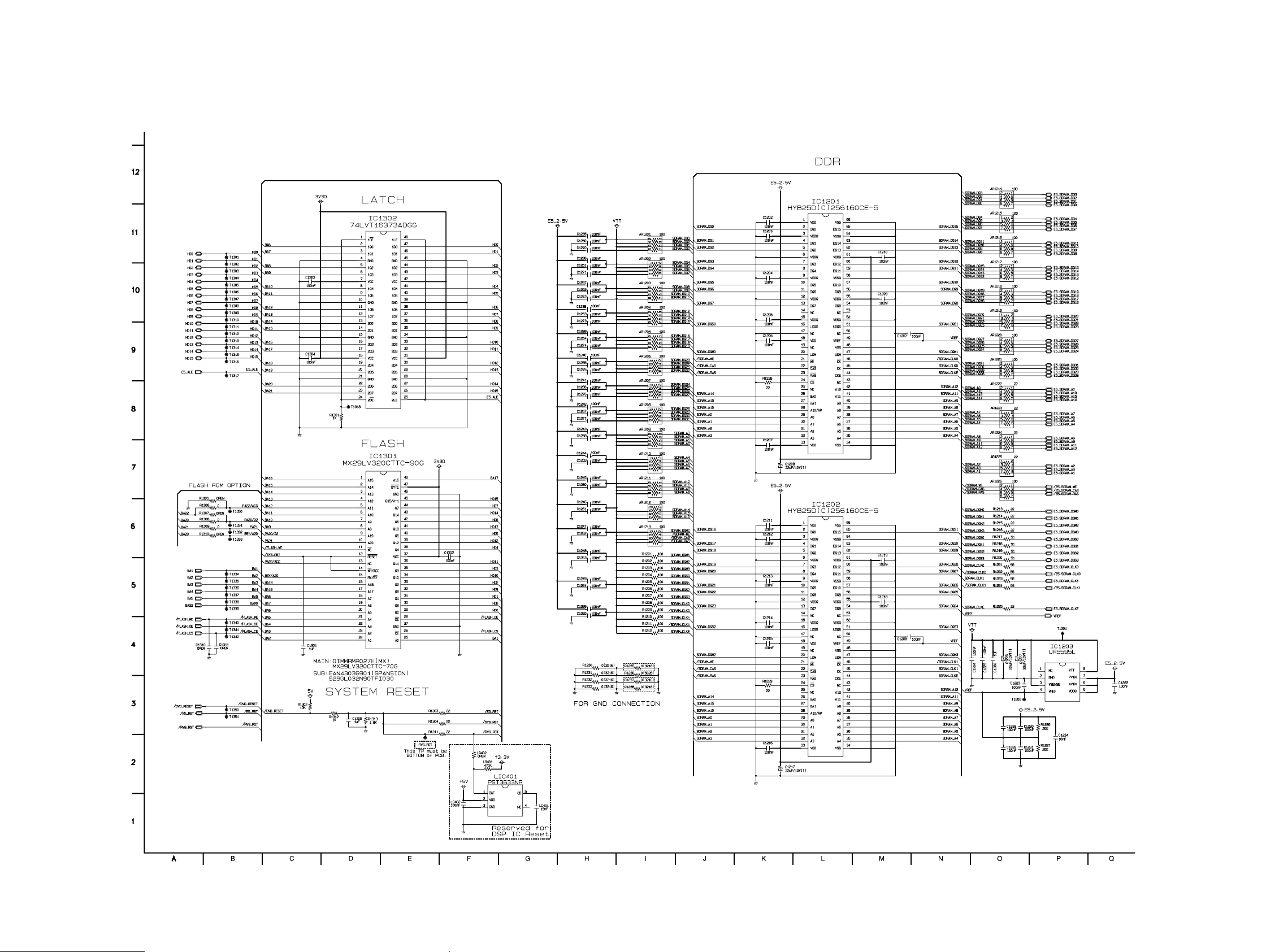
4-8. MAIN BOARD (DDR/LATCH/FLASH/RESET) SCHEMATIC DIAGRAM (2/5) • See page 5-3 for printed wiring board.
MAIN BOARD (2/5)
DDR/LATCH/FLASH/RESET
 Loading...