

Page 1
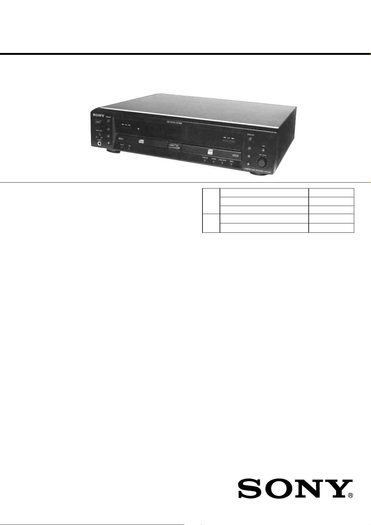
RCD-W3
SERVICE MANUAL
Ver 1.2 2003.12
SPECIFICATIONS
US Model
Canadian Model
AEP Model
UK Model
Model Name Using Similar Machanism RCD-W1
CD-R
CD Mechanism Type CDM-700(CD-RW)
Optical Pick-up Type KRS-220C
Model Name Using Similar Mechanism RCD-W1
CDP
CD Mechanism Type CDM-700(CDP)
DECK A (the CD player section)
System Compact disc and digital audio system
Laser Semiconductor laser (λ =780 nm)
Emission duration: continuous
Frequency response 20 Hz – 20,000 Hz (±0.5 dB)
Signal-to-noise ratio More than 100 dB
Dynamic range More than 95 dB
DECK B (the CD-R and CD-RW recording section)
System Compact disc digital audio system
Laser Semiconductor laser (λ =780 nm)
Emission duration: continuous
Playable discs CD, CD-R, CD-RW
Recordable discs CD-R, CD-RW (for music use)
Frequency response 20 to 20,000 Hz ±0.5 dB
Signal-to-noise ratio Over 100 dB during playback
Dynamic range More than 95 dB during playback
Inputs
ANALOG IN
(Phono jacks) impedance 47 kilohms
Rated input 330 mVrms
Minimum input 125 mVrms
DIGITAL OPTICAL IN
(Square optical connector jack) Optical wavelength 660 nm
Outputs
ANALOG OUT
(Phono jacks) Rated output 2 Vrms (at 50 kilohms)
Load impedance over 10 kilohms
OPTICAL DIGITAL OUT
(Square optical connector jack) Wavelength 660 nm
Output level -18 dBm
PHONES
(Phone jacks) 28 mW, 32 ohms
General
Power requirements
U.S.A. and Canada 120 V AC, 60 Hz
Other countries 110 – 240 V AC, 50/60 Hz
Power consumption 20 W
Dimensions (approx.) (w/h/d) incl. projecting parts and control
430 x 108 x 368 mm
Mass (approx.) 4.6 kg
Supplied accessories • Audio connecting cord (2)
• Remote commander (remote) (1)
• Size AA (R6) batteries (2).
Design and specifications are subject to change without notice.
9-874-117-03
2003L02-1
© 2003.12
COMPACT DISC RECORDER
Sony Corporation
Home Audio Company
Pubulished by Sony Engineering Corporation
Page 2
RCD-W3
NOTES ON HANDLING THE OPTICAL PICK-UP
BLOCK OR BASE UNIT
The laser diode in the optical pick-up block may suffer electrostatic
break-down because of the potential difference generated by the
charged electrostatic load, etc. on clothing and the human body.
During repair, pay attention to electrostatic break-down and also
use the procedure in the printed matter which is included in the
repair parts.
The flexible board is easily damaged and should be handled with
care.
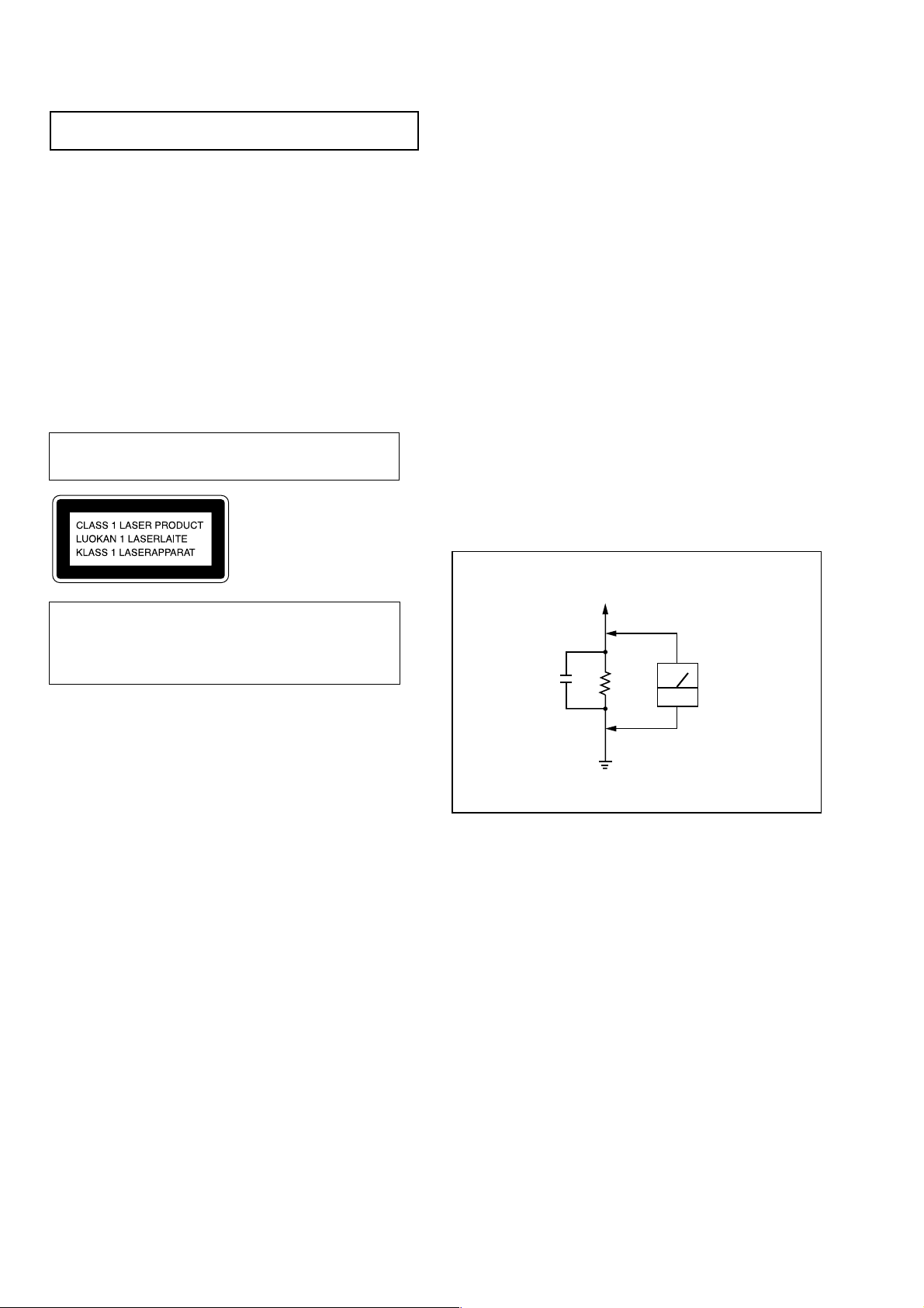
NOTES ON LASER DIODE EMISSION CHECK
The laser beam on this model is concentrated so as to be focused on
the disc reflective surface by the objective lens in the optical pickup block. Therefore, when checking the laser diode emission, observe from more than 30 cm away from the objective lens.
The Laser component in this product is capable of emitting
radiation exceeding the limit for Class 1.
This appliance is classified as
a CLASS 1 LASER product.
The CLASS 1 LASER PRODUCT MARKING is located on
the rear exterior.
CAUTION
Use of controls or adjustments or performance of procedures
other than those specified herein may result in hazardous radiation exposure.
Notes on chip component replacement
• Never reuse a disconnected chip component.
• Notice that the minus side of a tantalum capacitor may be
damaged by heat.
Flexible Circuit Board Repairing
• Keep the temperature of soldering iron around 270˚C
during repairing.
• Do not touch the soldering iron on the same conductor of the
circuit board (within 3 times).
• Be careful not to apply force on the conductor when soldering
or unsoldering.
SAFETY CHECK-OUT
After correcting the original service problem, perform the following safety checks before releasing the set to the customer:
Check the antenna terminals, metal trim, “metallized” knobs, screws,
and all other exposed metal parts for AC leakage. Check leakage as
described below.
LEAKAGE
The AC leakage from any exposed metal part to earth Ground and
from all exposed metal parts to any exposed metal part having a
return to chassis, must not exceed 0.5 mA (500 microampers). Leakage current can be measured by any one of three methods.
1. A commercial leakage tester, such as the Simpson 229 or RCA
WT-540A. Follow the manufacturers’ instructions to use these
instruments.
2. A battery-operated AC milliammeter. The Data Precision 245
digital multimeter is suitable for this job.
3. Measuring the voltage drop across a resistor by means of a VOM
or battery-operated AC voltmeter. The “limit” indication is 0.75
V, so analog meters must have an accurate low-voltage scale.
The Simpson 250 and Sanwa SH-63Trd are examples of a passive VOM that is suitable. Nearly all battery operated digital
multimeters that have a 2V AC range are suitable. (See Fig. A)
To Exposed Metal
Parts on Set
0.15µF
1.5kΩ
Earth Ground
AC
voltmeter
(0.75V)
Fig. A. Using an AC voltmeter to check AC leakage.
SAFETY-RELATED COMPONENT WARNING !!
COMPONENTS IDENTIFIED BY MARK ! OR DO TTED LINE
WITH MARK ! ON THE SCHEMATIC DIAGRAMS AND IN
THE PARTS LIST ARE CRITICAL TO SAFE OPERATION.
REPLACE THESE COMPONENTS WITH SONY PARTS
WHOSE PART NUMBERS APPEAR AS SHOWN IN THIS
MANUAL OR IN SUPPLEMENTS PUBLISHED BY SONY.
2
ATTENTION AU COMPOSANT AYANT RAPPORT
À LA SÉCURITÉ!!
LES COMPOSANTS IDENTIFIÉS P AR UNE MARQUE ! SUR
LES DIAGRAMMES SCHÉMATIQUES ET LA LISTE DES
PIÈCES SONT CRITIQUES POUR LA SÉCURITÉ DE
FONCTIONNEMENT. NE REMPLACER CES COMPOSANTS
QUE PAR DES PIÈCES SONY DONT LES NUMÉROS
SONT DONNÉS DANS CE MANUEL OU DANS LES
SUPPLÉMENTS PUBLIÉS PAR SONY.
Page 3

Error Messages
The following table explains the error messages that appear in the
display.
RCD-W3
TABLE OF CONTENTS
1. SERVICING NOTE .......................................................... 4
2. GENERAL .......................................................................... 8
Message Explanation
CHECK DISC • A record-related button has been
pressed when a finalized disc is in
the DECK B.
• A record-related button has been
pressed when a standard CD is in
the DECK B.
DATA DISC A non-audio CD-ROM or a CDVideo
disc has been placed in the machine.
DISC ERROR • An unfinalized disc has been placed in
the DECK A.
• There is a problem with the disc.
• A DVD disc has been placed in the unit.
DISC FULL There is not enough time left on the disc
to complete a planned recording.
ERROR There is a problem with the tray.
FAILED A dubbing has not been completed
properly.
FULL More than 20 tracks have been
programmed.
NO AUDIO A record-related button has been
pressed when a non-audio disc is in
the DECK B.
3. DISASSEMBLY
3-1. Top Case............................................................................... 9
3-2. Tray Door, Front Panel Assy.............................................. 10
3-3. HP board, FL board, VOL board........................................ 10
3-4. Back Panel ......................................................................... 11
3-5. Audio Board ....................................................................... 11
3-6. Power Board ...................................................................... 12
3-7. CDP Deck assy (Deck A), CD-R Deck Assy (Deck B) ..... 12
3-8. BD-P Board (Deck A) ........................................................ 13
3-9. CDP Mechanism Assy (Deck A)........................................ 13
3-10.Spindle Motor Assy, Optical Pick-Up Block (Deck A)...... 14
3-11.BD-R Board........................................................................ 14
3-12.CD-R Mechanism Assy (Deck B)...................................... 15
4. ELECTRICAL ADJUSTMENT ................................... 16
5. DIAGRAMS
5-1. Circuit Boards Location .................................................... 21
5-2. Block diagrams – CD-R Section (1/2) – ........................... 23
Block diagrams – CD-R Section (2/2) – ........................... 24
Block diagrams – CDP Section –...................................... 25
Block diagrams – Audio Section – ................................... 26
Block diagrams – Power Section – ................................... 27
5-3. Printed Wiring Board – BD-R Section (Side A) – ............ 28
Printed Wiring Board – BD-R Section (Side B) – ............ 29
5-4. Schematic Diagram – BD-R Section (1/6) –..................... 30
5-5. Schematic Diagram – BD-R Section (2/6) –..................... 31
5-6. Schematic Diagram – BD-R Section (3/6) –..................... 32
5-7. Schematic Diagram – BD-R Section (4/6) –..................... 33
5-8. Schematic Diagram – BD-R Section (5/6) –..................... 34
5-9. Schematic Diagram – BD-R Section (6/6) –..................... 35
5-10. Printed Wiring Board – Audio Section –........................... 36
5-11. Schematic Diagram – Audio Section – ............................ 37
5-12. Printed Wiring Board – Panel Section – ........................... 38
5-13. Schematic Diagram – Panel Section – ............................. 39
5-14. Printed Wiring Board – Power Section – ......................... 40
5-15. Schematic Diagram – Power Section – ............................ 41
5-16. Printed Wiring Board – BD-P Section –........................... 42
5-17. Schematic Diagram – BD-P Section – ............................. 42
5-18. IC Pin Functions Description ........................................... 43
5-19. IC Block Diagrams ........................................................... 48
6. EXPLODED VIEWS
6-1. Front Panel Section ............................................................. 52
6-2. Chassis Section ................................................................... 53
6-3. CD Play Section (Deck A) .................................................. 54
6-4. CD Record Section (Deck B).............................................. 55
7. ELECTRICAL PARTS LIST .................................56
3
Page 4
RCD-W3
SECTION 1
SERVICING NOTE
NOTES REGARDING HANDLING OF THE PICK-UP
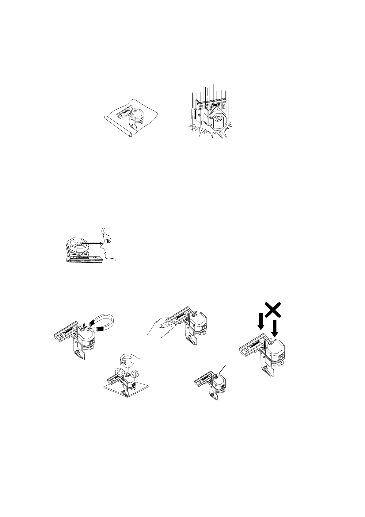
1. Notes for transport and storage
1) The pick-up should always be left in its conductive bag until immediately prior to use.
2) The pick-up should never be subjected to external pressure or impact.
Storage in conductive bag
Drop impact
2. Repair notes
1) The pick-up incorporates a strong magnet, and so should never be brought close to magnetic materials.
2) The pick-up should always be handled correctly and carefully , taking care to avoid external pressure and impact.
If it is subjected to pressure or impact, the result may be an operational malfunction and/or damage to the
printed-circuit board.
3) Each and every pick-up is already individually adjusted to a high degree of precision, and for that reason the
adjustment point and installation screws should absolutely never be touched.
4) Laser beams may damage the eyes!
Absolutely never permit laser beams to enter the eyes!
Also NEVER switch ON the power to the laser output part (lens, etc.) of the pick-up if it is damaged.
NEVER look directly at the laser beam, and don’t let contact
fingers or other exposed skin.
5) Cleaning the lens surface
If there is dust on the lens surface, the dust should be cleaned away by using an air bush (such as used for
camera lens). The lens is held by a delicate spring. When cleaning the lens surface, therefore, a cotton swab
should be used, taking care not to distort this.
Pressure
Magnet
How to hold the pick-up
Cotton swab
Conductive Sheet
6) Never attempt to disassemble the pick-up.
Spring by excess pressure. If the lens is extremely dirty, apply isopropyl alcohol to the cotton swab. (Do not use any
other liquid cleaners, because they will damage the lens.) Take care not to use too much of this alcohol on the swab,
and do not allow the alcohol to get inside the pick-up.
Pressure
4
Page 5
NOTES REGARDING COMPACT DISC PLAYER REPAIRS
1. Preparations
1) Compact disc players incorporate a great many ICs as well as the pick-up (laser diode). These components are sensitive to, and easily affected by, static electricity. If such static is high voltage, components
can be damaged, and for that reason components should be handled with care.
2) The pick-up is composed of many optical components and other high-precision components. Care must
be taken, therefore, to avoid repair or storage where the temperature of humidity is high, where strong
magnetism is present, or where there is excessive dust.
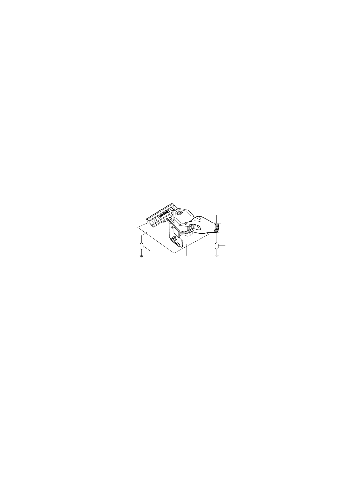
2. Notes for repair
1) Before replacing a component part, first disconnect the power supply lead wire from the unit
2) All equipment, measuring instruments and tools must be grounded.
3) The workbench should be covered with a conductive sheet and grounded.
When removing the laser pick-up from its conductive bag, do not place the pick-up on the bag. (This is
because there is the possibility of damage by static electricity.)
4) To prevent AC leakage, the metal part of the soldering iron should be grounded.
5) Workers should be grounded by an armband (1MΩ)
6) Care should be taken not to permit the laser pick-up to come in contact with clothing, in order to prevent
static electricity changes in the clothing to escape from the armband.
7) The laser beam from the pick-up should NEVER be directly facing the eyes or bare skin.
RCD-W3
Resistor
(1MΩ)
Armband
Resistor
(1MΩ)
Conductive
Sheet
5
Page 6

RCD-W3
Electrostatically Sensitive Devices (ESD)
Some semiconductor (solid state) devices can be damaged easily by static electricity. Such components commonly are called Electrostatically Sensitive Devices (ESD). Examples of typical ESD devices are integrated circuits and some field-effect transistors and semiconductor chip components. The following techniques should
be used to help reduce the incidence of component damage caused by static electricity.
1. Immediately before handling any semiconductor component or semiconductor-equipped assembly, drain off
any electrostatic charge on your body by touching a known earth ground. Alternatively, obtain and wear a
commercially available discharging wrist strap device, which should be removed for potential shock reasons
prior to applying power to the unit under test.
2. After removing an electrical assembly equipped with ESD devices, place the assembly on a conductive surface such as aluminum foil, to prevent electrostatic charge buildup or exposure of the assembly.
3. Use only a grounded-tip soldering iron to solder or unsolder ESD devices.
4. Use only an anti-static solder removal device. Some solder removal devices not classified as "anti-static" can
generate electrical charges sufficient to damage ESD devices.
5. Do not use freon-propelled chemicals. These can generate electrical charges sufficient to damage ESD devices.
6. Do not remove a replacement ESD device from its protective package until immediately before you are ready
to install it. (Most replacement ESD devices are packaged with leads electrically shorted together by conductive
foam, aluminum foil or comparable conductive materials).
7. Immediately before removing the protective material from the leads of a replacement ESD device, touch the
protective material to the chassis or circuit assembly into which the device will by installed.
CAUTION : BE SURE NO POWER IS APPLIED TO THE CHASSIS OR CIRCUIT, AND OBSERVE ALL
OTHER SAFETY PRECAUTIONS.
8. Minimize bodily motions when handing unpackaged replacement ESD devices. (Otherwise harmless motion
such as the brushing together of your clothes fabric or the lifting of your foot from a carpeted floor can gen erate static electricity sufficient to damage an ESD device).
6
Page 7
RCD-W3
)
NOTE ON CHECKING POWER SUPPLY CIRCUIT
1. When check the primary part, you must remove the GND pin of
the scope and soldering machine.
Primary GND : C103 – terminal at power board.
2. When check the primary part, you must open the another GND(not
used GND) of scope.
(If another scope GND is connected to secondary GND or other
system, input power line or system have some damage.)
3. When touch the primary part by hand in defected system,
if you use the power line switch, remove the power cord and then
check or touch.
Because in general power switch is switching only one line.
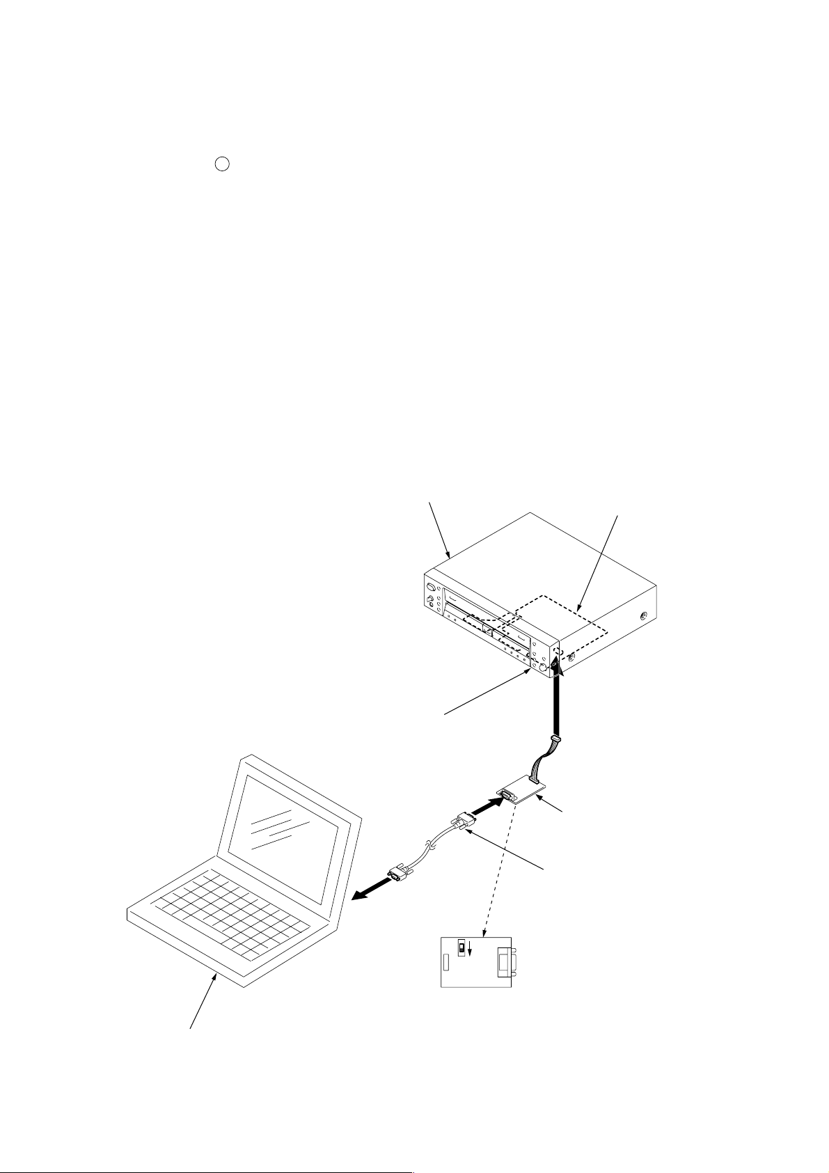
BD-R BOARD CHECK AND ADJUSTING JIGS
In case of checking or adjusting the LD power of BD-R board, the PC connection jig (J-2501-210-A) and the test program are required.
This test program is distributed with the service manual.
4. When check the primary part, after remove power cord and dis
charge the primary capacitor, and then check the system.
In the normal state, the voltage of the capacitor is small
(about 10V), but in the abnormal state is very high ( about 140V
at 100V A.C or 300V at 220V).
When discharge the capacitor , use the wattage resistor(about 100
ohm).
5. In the narrow system, Until set repaired completely,
insert the power cord at the moment repeatedly and then check
the waveform.
6. In the wide system, when insert the power cord, check the wave
form after about 3 second.
Because the wide system is the soft start method.
RCD-W3
CD-R
test connector (PN105)
BD-R board
PC connection jig
(J-2501-210-A)
PS-232C cable (D-sub 9pin
(straight type)
PC
SW501
W
D
CNP501CN505
PC connection jig
Set SW501 to “D” side
7
Page 8
RCD-W3
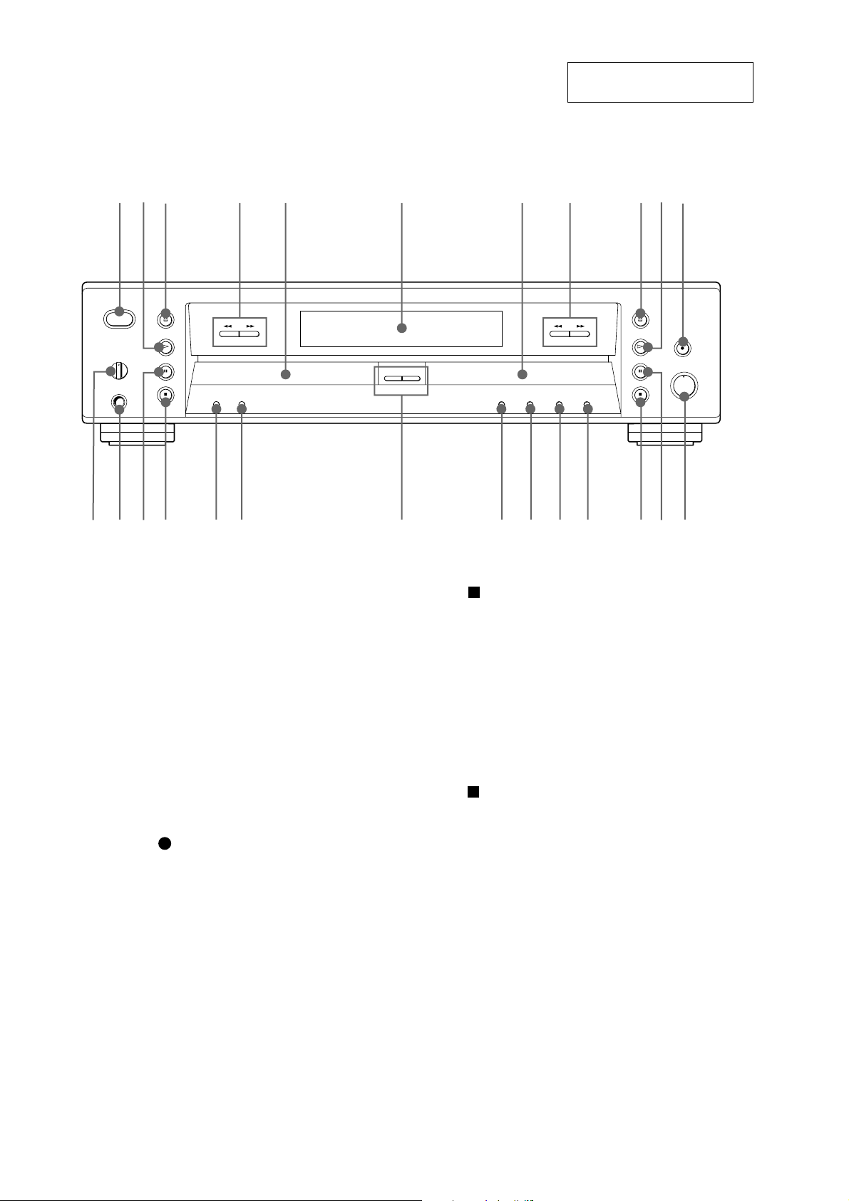
Parts and Controls
SECTION 2
GENERAL
123 4 5 6 7 8 90qa
This section is extracted from
instruction manual.
1 POWER button
2 H (play) button -Deck A
3 OPEN/CLOSE A button -Deck A
4 . AMS > buttons -Deck A
5 Disc tray-Deck A
6 Display window
7 Disc tray-Deck B
8 . AMS > buttons -Deck B
9 OPEN/CLOSE A button -Deck B
0 H (play) button -Deck B
qa REC button -Deck B
qs REC LEVEL knob
qd X (pause) button -Deck B
qfqgqhqjqkqlw;wawswdwfwg qd qs
qf (stop) button -Deck B
qg INPUT button
qh LEVEL SYNC button
qj ERASE button
qk FINALIZE button
ql CD SYNCHRO NORMAL/HIGH buttons
w; TIME button
wa RELAY button
ws (stop) button -Deck A
wd X (pause) button -Deck A
wf PHONES jack
wg PHONE LEVEL knob
8
Page 9
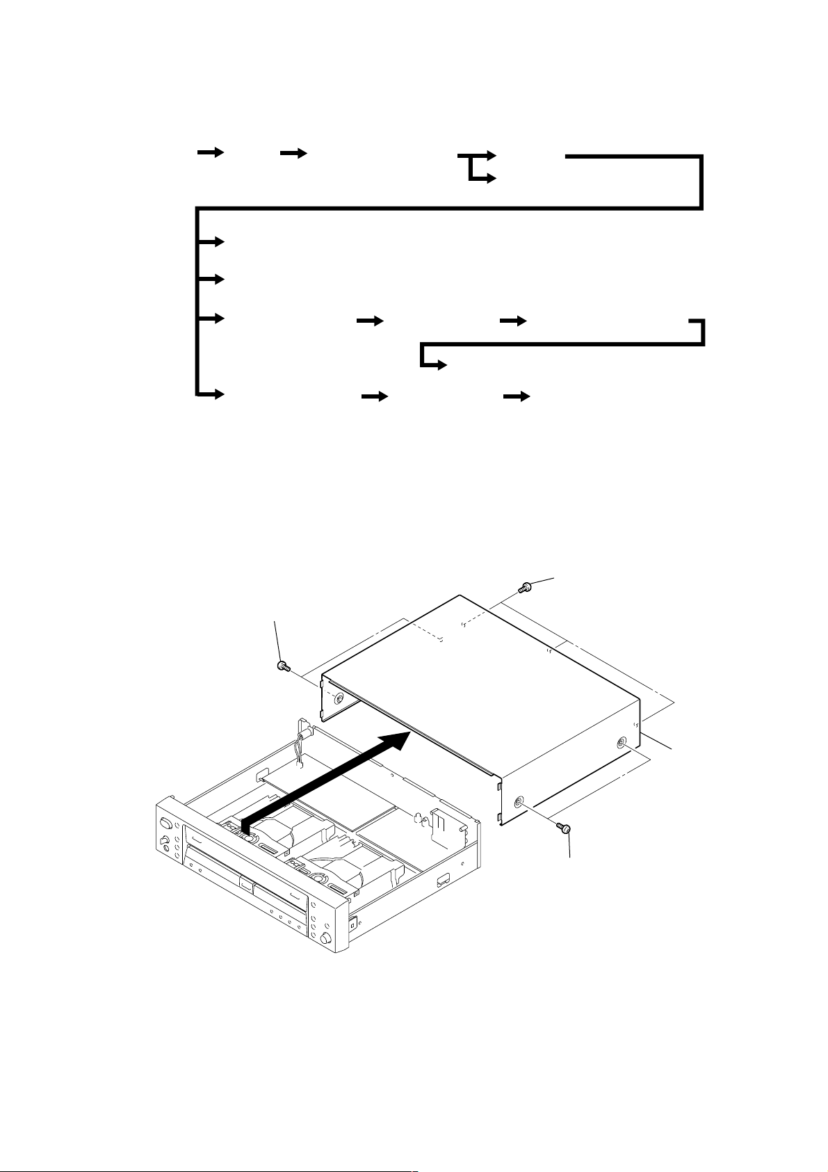
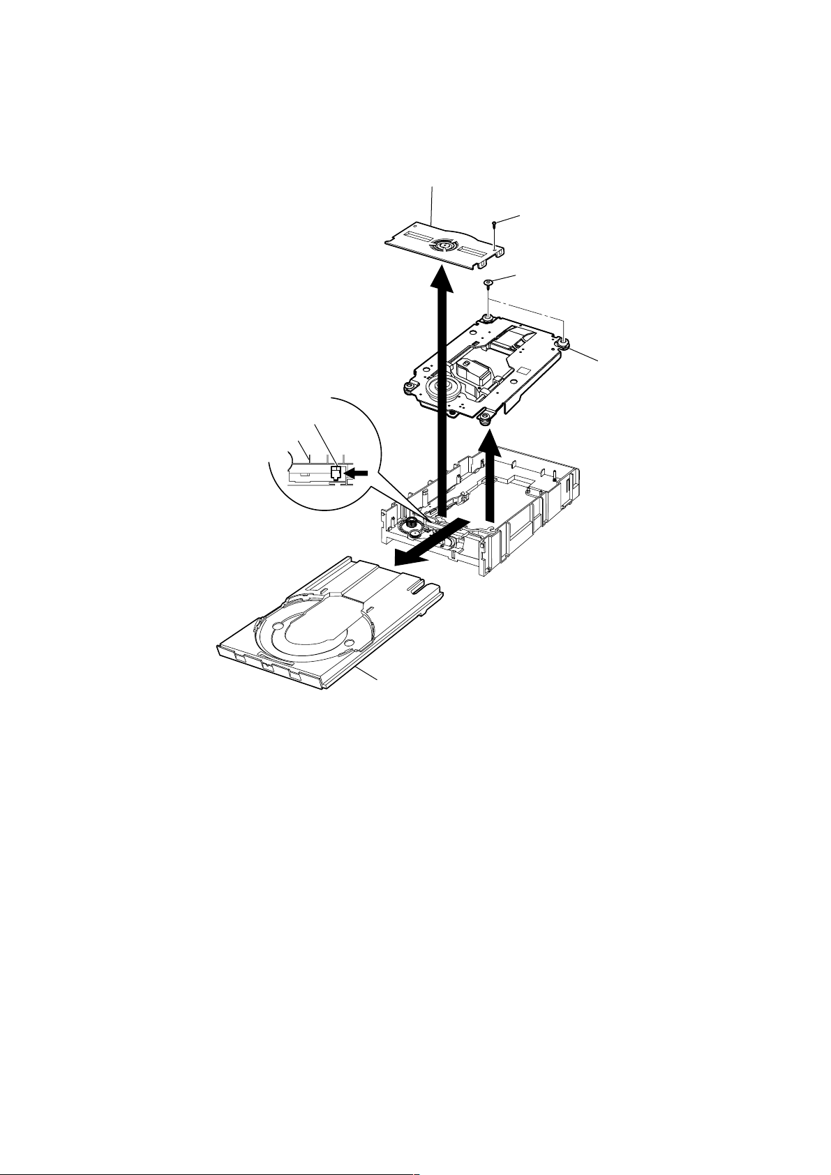
Note: Disassemble the unit in the order as shown below.
e
RCD-W3
SECTION 3
DISASSEMBLY
Set
Note: Follow the disassembly procedure in the numerical order given.
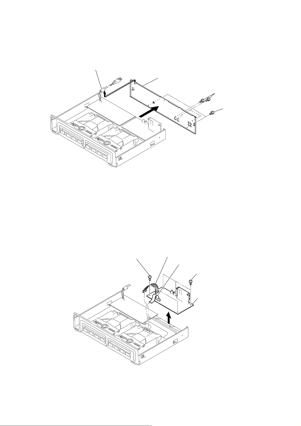
Top case
Audio board
Power board
CDP deck assy (deck A)
CD-R deck assy (deck B)
Tray door, Front panel assy
BD-P board (deck A)
BD-R board (deck B)
3-1. T OP CASE
Back panel
HP board, FL board, VOL board
CDP mechanism assy (deck A)
Spindle motor assy, Optical pick-up block (deck A)
CD-R mechanism assy (deck B)
2
Two screws (case)
4
3
Three screws (case)
1
Two screws (case)
5
Top cas
9
Page 10
RCD-W3
)
3-2. TRAY DOOR, FRONT PANEL ASSY
1
Insert a screwdriver to the square hole on the bottom,
and slide the white lever in the arrow Adirection to
open the tray.
Then remove the tray door.
(In the case of DECK B, remove it in the same manner.)
White lever
A
7
5
Connector (PN902)
4
Connector (PN401)
3
Connector (CN704)
2
Connector (CN702
Tray door (Play)
(deck A)
Tray door (Rec)
(deck B)
3-3. HP BOARD, FL BOARD, VOL BOARD
6
POWER knob
4
6
Claws
8
7
Screw (Special)
8
5
PWB holder
0
Two screws (Special)
Front panel assy
HP board
3
Two screws (Special)
10
2
P/VOLUME knob
qa
Claws
qs
FL board and VOL board
Front panel
1
REC VOL knob
9
Four screws (Special)
Page 11
3-4. BACK PANEL
)
)
3
Cord power
4
5
Back panel
1
Four screws (3X10)
2
Two screws (3X8 BK
RCD-W3
3-5. AUDIO BOARD
3
Two screws (special)
2
Connector (PN201)
1
Wire (flat type) (PN501)
5
4
Three screws (special
6
AUDIO board
11
Page 12
RCD-W3
3-6. POWER BOARD
1
Connector (PN503)
2
Two screws (special)
4
3
Two screws (special)
5
POWER board
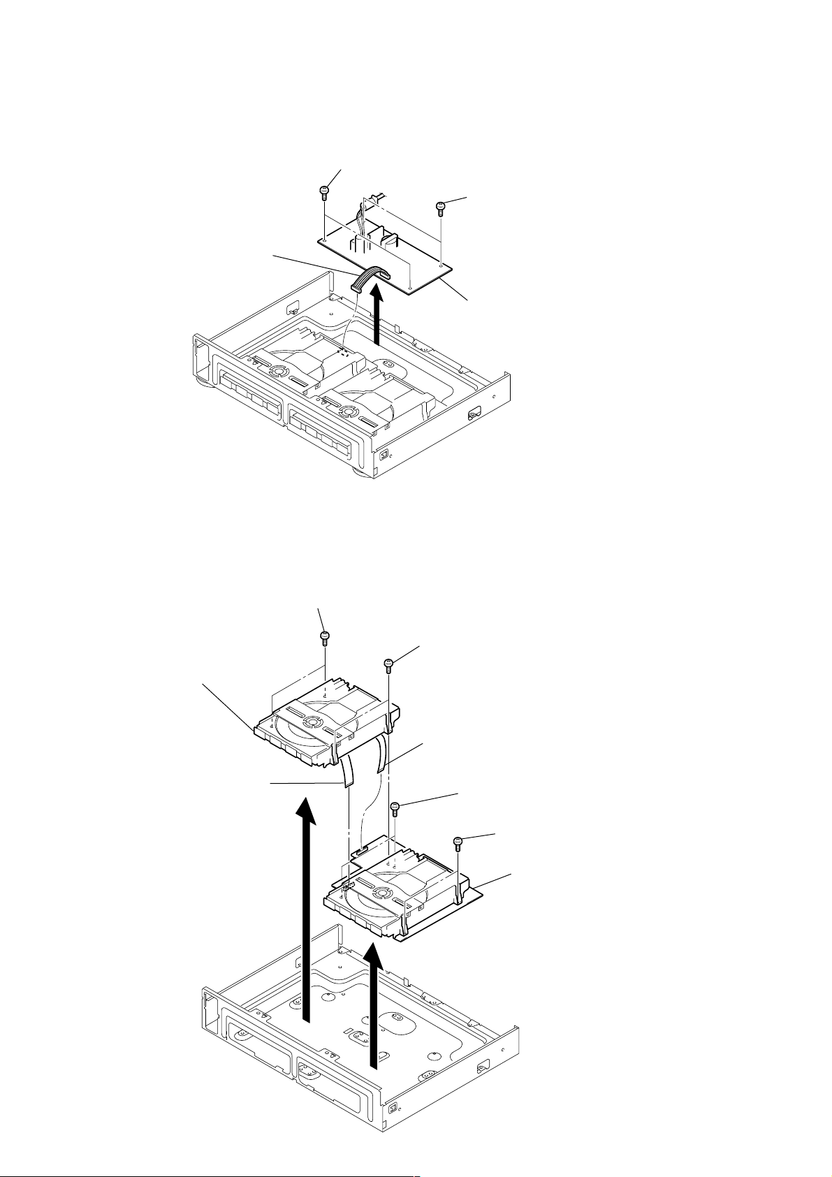
3-7. CDP DECK ASSY (DECK A), CD-R DECK ASSY (DECK B)
2
Two screws (special)
3
Two screws (special)
6
CDP deck assy (deck A)
5
1
Wire (flat type)
(PN403)
4
9
Wire (flat type)
(PN406)
7
Two screws (special)
8
Two screws (special)
0
CD-R deck assy (deck B)
12
Page 13
3-8. BD-P BOARD (DECK A)
)
y
1
Wire (flat type) (PN4M3)
5
Connector (PN4M5)
3
Claw
4
6
BD-P board
1
Wire (flat type) (PN4M4
RCD-W3
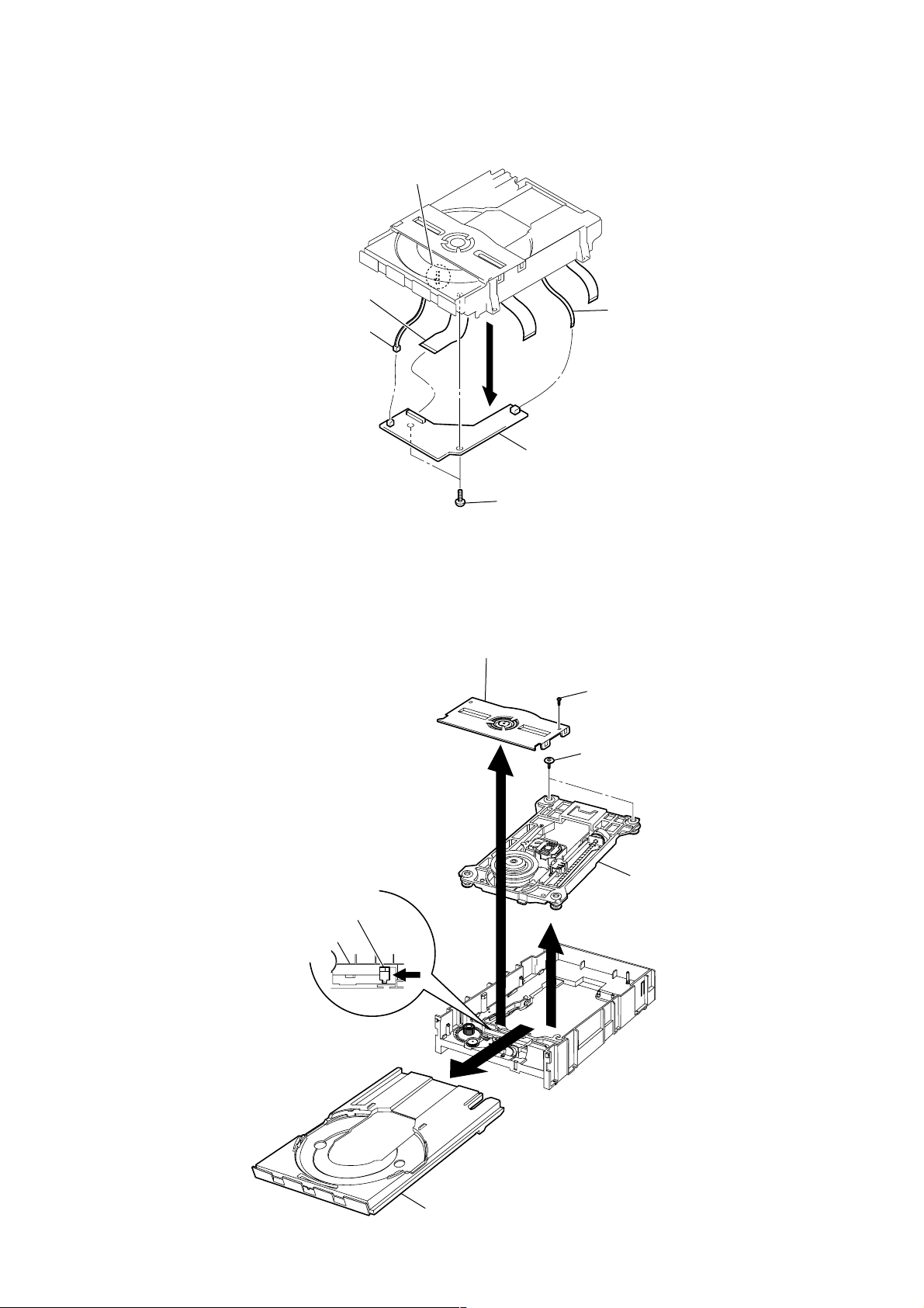
3-9. CDP MECHANISM ASSY (DECK A)
4
Push out the disc tray by pushing the
Up/Down guide un the drrow
Up/Down guide
Main base
A
direction.
A
2
Two screws (2X6)
3
Clamp holder assy
2
1
Screw (1.7X6)
7
Two screws (2.0X10)
9
8
CDP mechanism ass
Bottom view
6
Disc tray
5
13
Page 14
RCD-W3
k
)
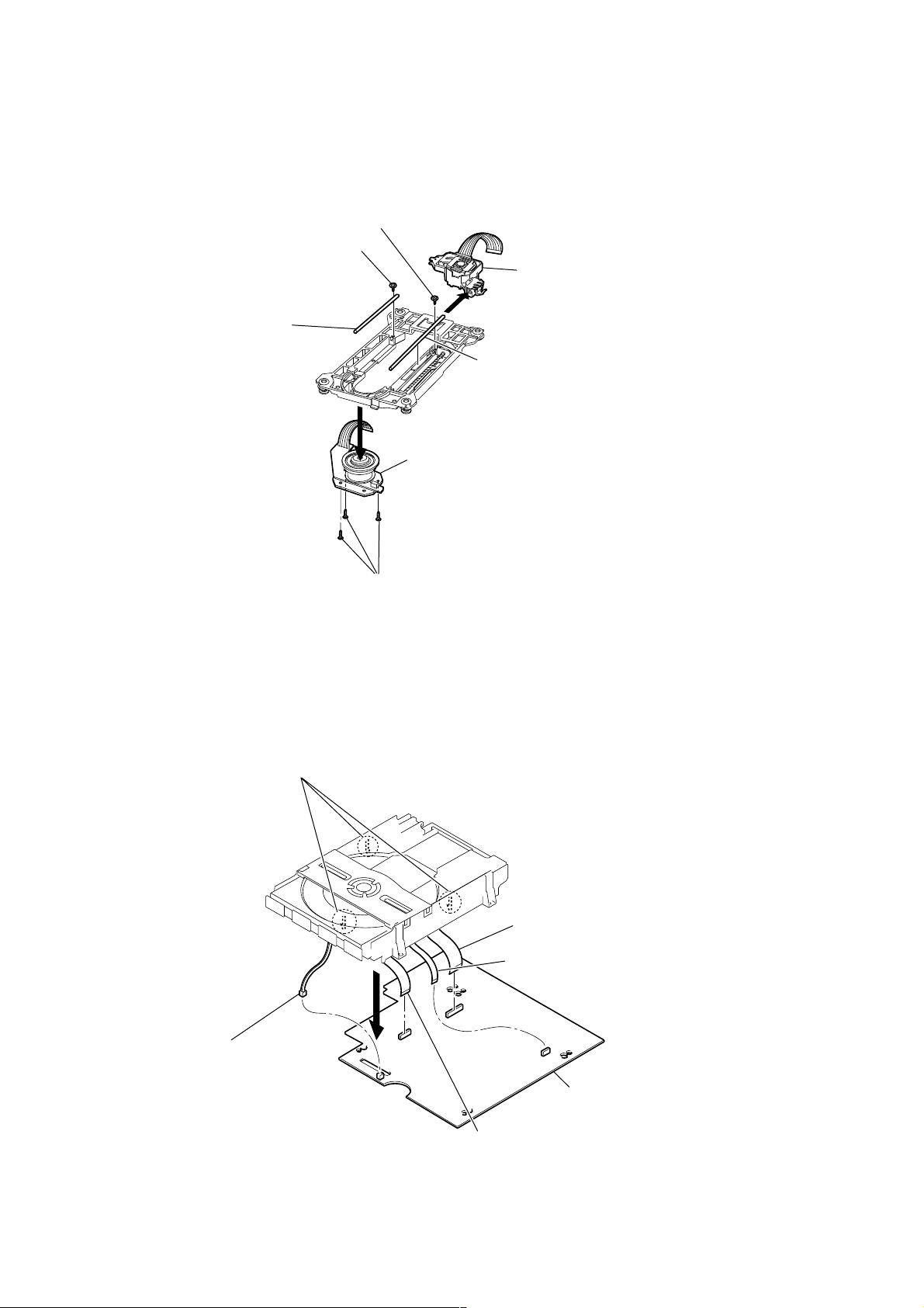
3-10. SPINDLE MOTOR ASSY, OPTICAL PICK-UP BLOCK (DECK A)
5
Screw (1.7X5)
3
Screw (1.7X5)
8
Optical pick-up bloc
4
3-11. BD-R BOARD (DECK B)
Shaft L
2
Spindle motor assy
1
Three screws (2X6)
7
6
Shaft R
3
Connector (PN302)
1
Three claws
6
4
Wire (flat type) (PN301
2
Wire (flat type) (PN303)
5
Wire (flat type) (PN304)
7
BD-R board
14
Page 15
3-12. CD-R MECHANISM ASSY (DECK B)
4
Push out the disc tray by pushing the
Up/Down suide un the drrow
Up/Down guide
Main base
A
direction.
A
3
Clamp holder assy
2
1
Screw (2X6)
7
Two screws (2.0X10)
8
9
CD-R mechanism assy
RCD-W3
Bottom view
6
Disc tray
5
15
Page 16
RCD-W3
SECTION 4
ELECTRICAL ADJUSTMENT
LD Power Adjustment
Jigs used on this adjustment
• LD Power Meter
A laser power meter 10mW or more measurable is required. Don’t use the laser power meter for Mini disc because of 10mW max.
Optical power meter (TQ8210): Product of ADVANTEST (on the market).
A thin type optical sensor (Q82017A): Product of ADVANTEST (on the market).
• PC Connection Jig (J-2501-210-A)
• Test Program FD
Dragon program Tool DV810 Ver. 0.9A
(This test program is distributed with the service manual.)
• PC (Windows 95/98)
• RS-232C Cable (on the market) D-SUB 9 pin, straight type
• Test Disc for Operation Check
A low reflecting rate disc for checking playback performance. OK: It can be played back.
• Low reflecting CD-R disc: TCD-R082LMT (J-2502-063-1)
• Low reflecting CD-RW disc: TCD-W082L (J-2502-063 -2)
• CD test disc (YEDS-18) (3-702-101-01)
• Extension cable (4p, 1.0mm) (J-8000-023-A)
Laser Power Adjustment (CD-R Only)
In case of the following parts are replaced, this adjustment is required.
1. CD-R optical pick-up block (KRS-220C)
2. IC208 (EP- ROM)
Specification of Dragon Program Usage Environment
The Dragon Program programmed by API function of Windows 95 can be surely operated on the W indows 95/98 platform.
It isn’t guaranteed on the other platform.
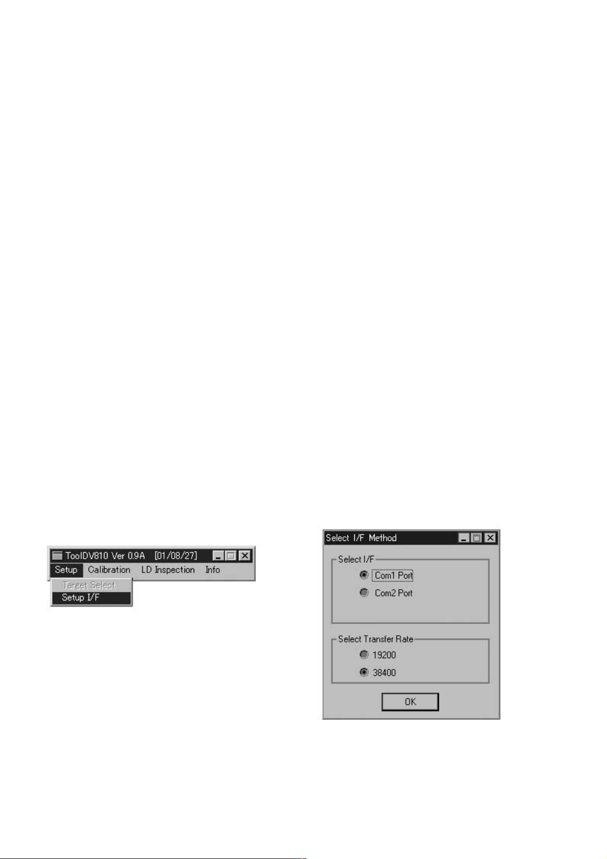
Start up
Procedure:
1. Connect the PC connection jig with the RS-232C cable between the test connector (PN105) on CD-R of RCD-W3 and COM port on
PC.(Check SW501 on the PC connection jig to “D” side.)
2. Turn power on RCD-W3.
3. Execute Dragon_dv810_svc.exe on Windows.
(Two files Dragon_dv810_svc.exe and Dragon_dv810.cfg are displayed on the setup menu window.)
4. Select “Setup I/F” on “Setup” pull-down menu, then “Select I/F Method” window is open.
5. Select Com Port matching to the Com Port connected the PC connection jig.
6. Select “38400” of “Select Transfer Rate”.
7. Click OK.
Fig 1 : Dragon menu and setup menu windows
16
Fig 2 : Select I/F method window
Page 17
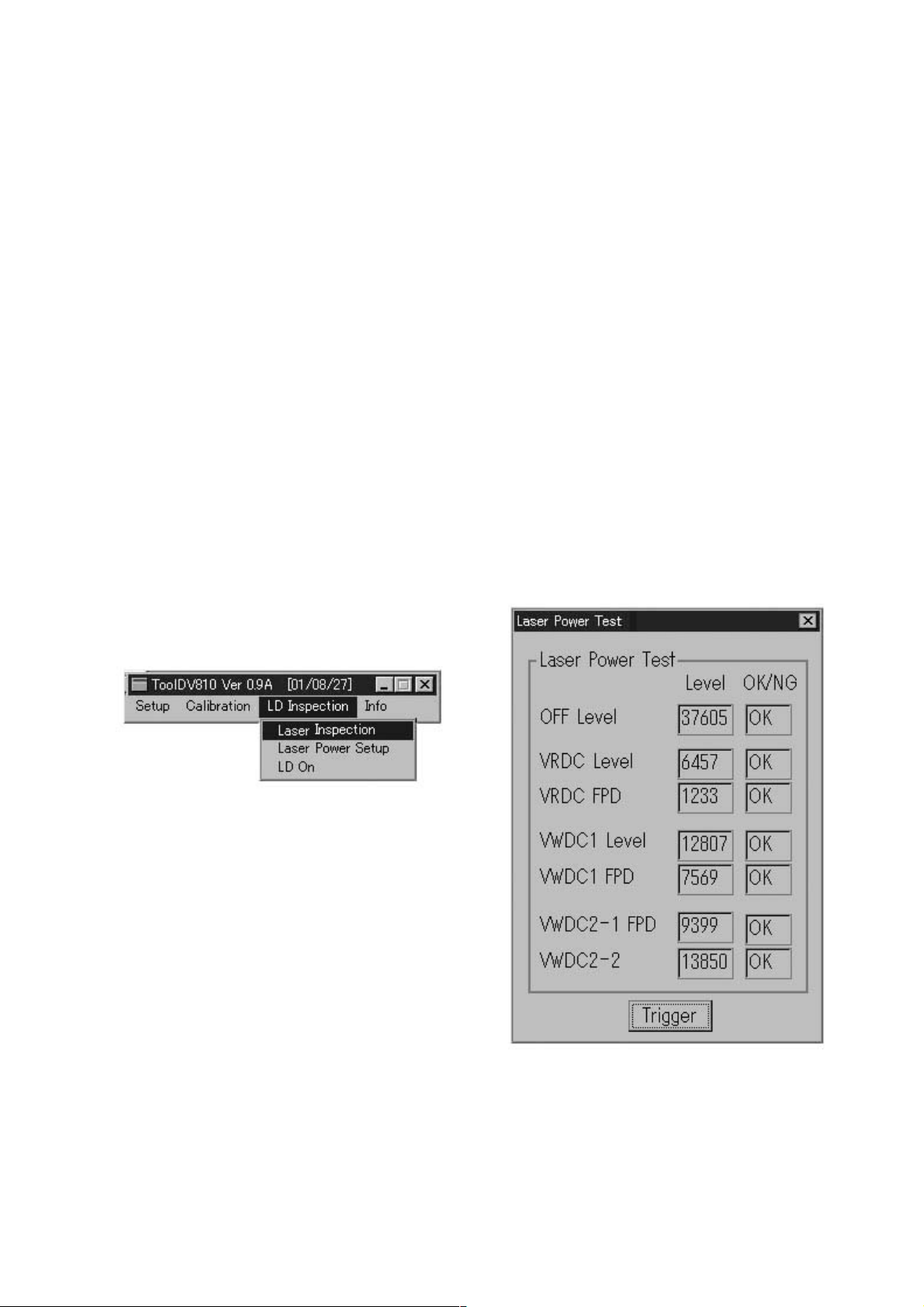
CD-R LD Setting Check
(VRDC/VWDC/FPD Level Value Check)
This routine is for checking performances of the record/playback D-A converter (IC304), the encoder/decoder IC
(IC301), CPLD (IC207), the optical pick-up block (KRS-220C), the microcomputer(IC203) and so on.
It diagnoses malfunctions of interface, the pick-up or so on.
It diagnoses the circuit in the recording mode without disc.
Description of each item
OFF LEVEL: In case of the laser turns off, FPDO output is 3V. Sampling value at this time.
VRDC LEVEL: APC circuit VRDC signal sampling value after READ power setting.
VRDC FPD: Optical pick-up FPDO signal sampling value after READ power setting.
VWDC1 LEVEL:APC circuit VWDC signal sampling value after setting WRITE power to regular value.
VWDC1 FPD: Optical pick-up FPDO signal sampling value after setting WRITE power to regular value.
VWDC2-1 FPD: There are two types of characteristics because of a non-linearity period of laser diode in the
over drive portion. This is FPDO sampling value in case of setting one of them to VWDC2 value.
VWDC2-2 FPD: FPDO sampling value in case of setting the other to VWDC2 value.
Specification of each item
38400-3300<OFF_LEVEL<38400+3300 (3.0±0.25V)
10<VRDC_LEVEL<20000
880<VRDC_FPD<1320
2000<VWDC1_LEVEL<25000
6160<VWDC1_FPD<12960
10<VWDC2-1_FPD<15000
2500<VWDC2-2_FPD<20000
Procedure:
1. Eject a disc from CD-R.
2. Select “Laser Inspection” on “LD Inspection” pull-down menu, then “Laser Power Test” window is open.
3. Click Trigger to execute LD check.
4. LD checked results are displayed.
(“OK”/“NG” is displayed for every items.)
5. Click X to close “Laser Power Test” window.
RCD-W3
Fig 3 : LD inspection menu windows
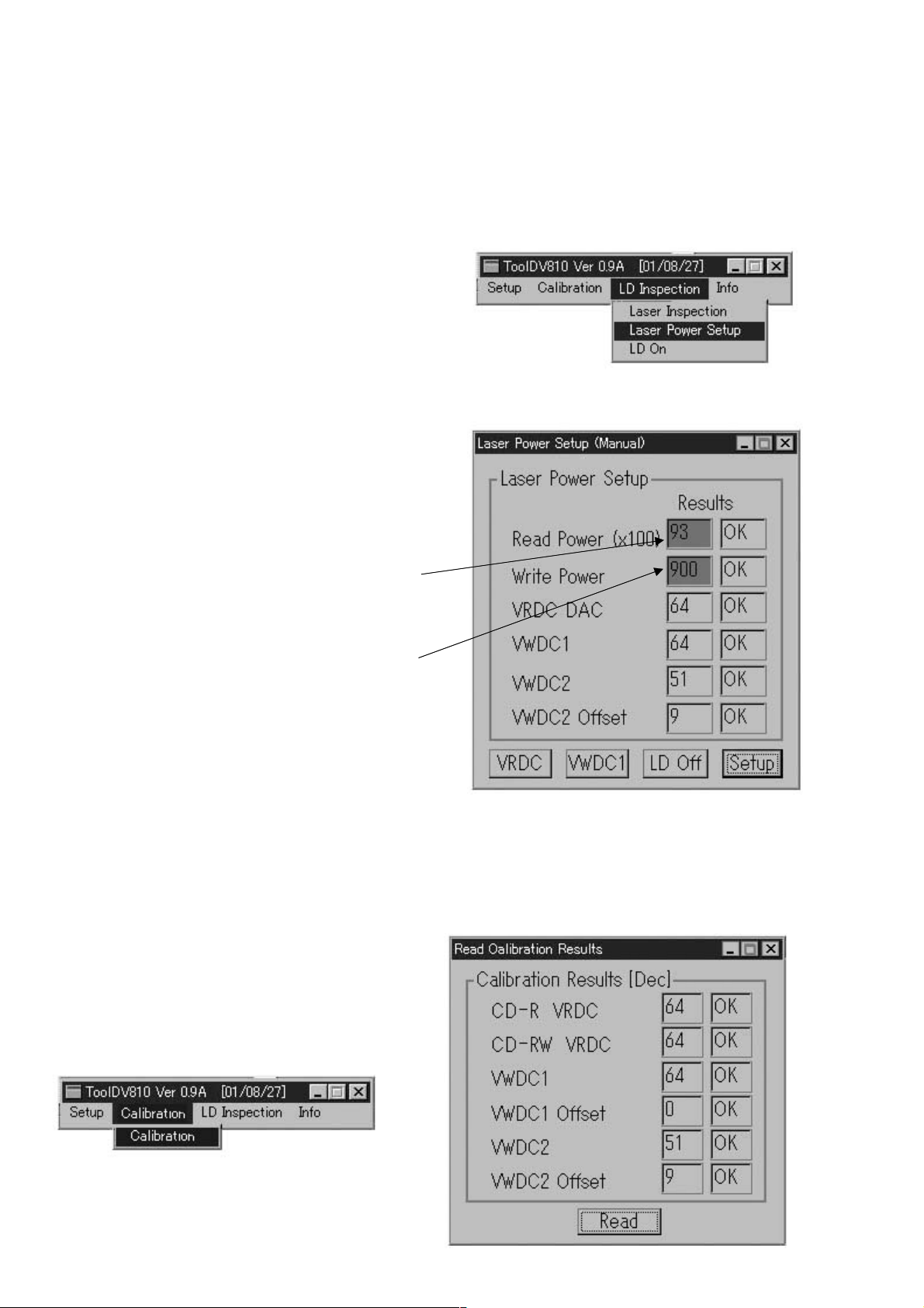
CD-R LD Power Setting
(VRDC/VWDC1 Resetting)
The optical pick-up and ICs in the circuit have a characteristics individually. In this routine, the parameters related to the
recording/playback power are actually measured and set properly.
The parameters are VRDC, VWDC1, VWDC2, VWDC2 Offset and so on. The reading power and playback power are set
properly by computing the related parameters on the basis of actually measuring values.
The preset parameters are used on power setting in case of performing Read/Write CD-R, CD-RW and so on.
Actual operation: The microcomputer receives serial data, then executes the related performances, and send parameter values to PC.
PC checks its related parameters and judges OK/NG.
Fig 4 : Laser power test window
17
Page 18
RCD-W3
Description of each parameter
VRDC: Used on the Read Power setting in case of reading CD-RW and CD-R. (DAC value on 100mW.)
VWDC: There is VWDC1 (Write power) pin in the optical pick-up block. The recording power is set by it and VWDC2
(Over drive) pin. Used on setting VWDC1 pin power on recording. (Unit: DAC value/10mW)
VWDC2: Used on setting VWDC2 (Over drive) pin power on recording. (Unit: DAC value/5mW)
VWDC2 Offset: Used on setting VWDC2 (Over drive) pin power with VWDC2 parameter on recording. (Unit: DAC value)
Specification of each parameter
20<read power<200
100<write power<2000
30<VRDC<150
48<VWDC1<150
50<VWDC2<145
VWDC2 Offset<35
Fig 5 : LD inspection menu windows
Procedure:
1. Eject a disc from CD-R.
2. Select “Laser Power Setup” on “LD Inspection” pull-down
menu, then “Laser Power Setup (Manual)” window is open.
3. Click VRDC, then Pick-up moves outward and LD turns on.
4. Measure the LD power with a LD power meter. W rite its value
to the blank of “Read Power” column.
(Write a value to two decimal places. Ex: W rite “93” in case of
0.93mW.)
5. Click VWDC1, then LD turns on.
6. Measure the LD power with a LD power meter. W rite its value
to the blank of “Write Power” column.
(Write a value to two decimal places. Ex: W rite “1234” in case
of 12.34mW.)
7. Click LD Off to turn LD off.
8. Click Setup, then setting is over and a result is displayed.
(“OK”/“NG” is displayed for every items.)
9. Click X to close “Laser Power Setup (Manual)” window.
Adjustment Data Check
Check if the error has occurred on reading “CD-R LD POWER SETTING” value.
Procedure:
1. Select “Calibration” on “Calibration” pull-down menu, then “Read Calibration Results” window is open.
2. Click Read, then the calibration data are displayed.
3. Data specification
CD-R VRDC DAC: 30-150
VWDC1: 48-150
VWDC2: 50-145
VWDC2 Offset: 0-35
4. Click X to close “Read Calibration Results” window.
Fig 7 : Calibration menu windows
Fig 6 : Laser power setup window
18
Fig 8 : Read calibration results window
Page 19
RCD-W3
level=1.3±0.6Vp-p
symmetry
A (DC voltage)
center of
waveform
B
0V
1 track jump waveform
Specified level: –– × 100=less than ±22%
B
A
e
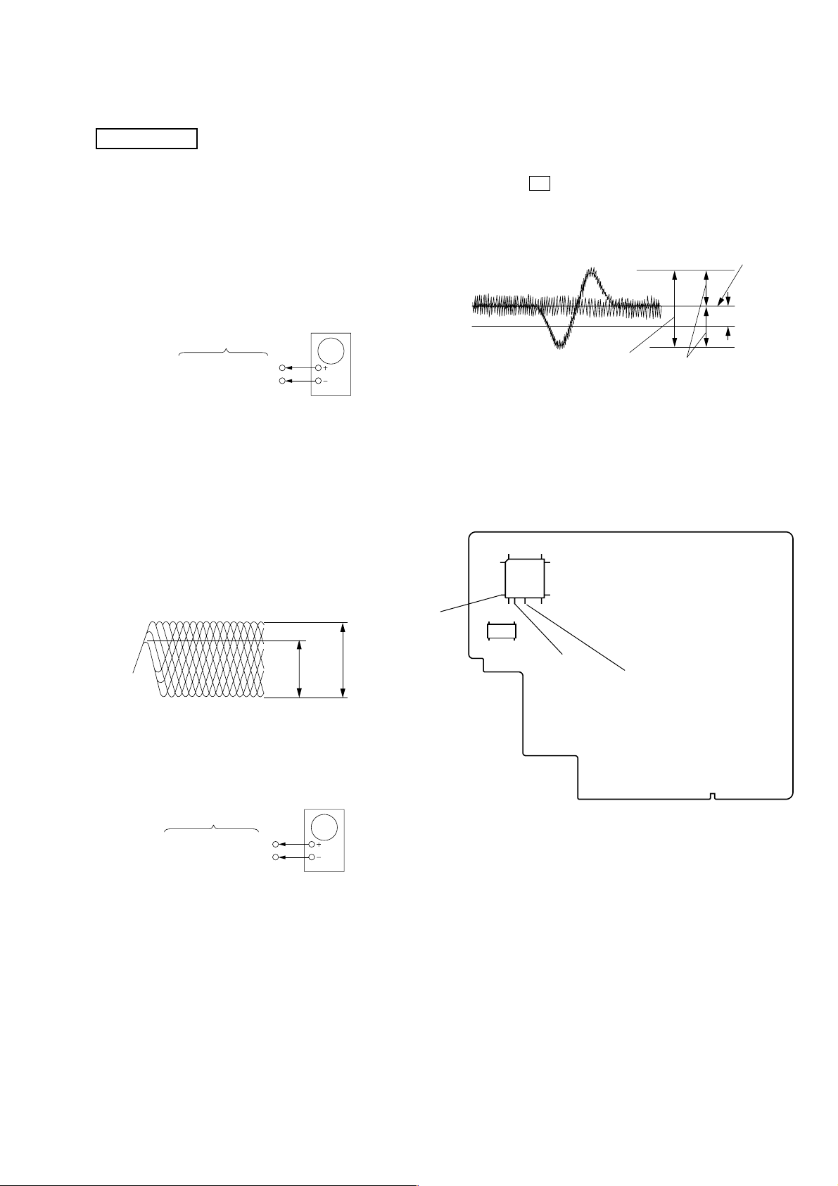
SERVO Check
CD SECTION
Note :
1. CD Block is basically designed to operate without adjustment.
Therefore, check each item in order given.
2. Use YEDS-18 disc unless otherwise indicated.
3. Use an oscilloscope with more than 10MΩ impedance.
4. Clean the object lens by an applicator with neutral detergent
when the signal level is low than specified value with the following checks.
RF Level Check
oscilloscope
BD-R board
IC402 ehpin(RFAC)
IC402 wkpin(VC)
Procedure :
1. Connect oscilloscope to IC402 eh pin (RFAC) and IC402 wk
pin (VC).
2. Turned Power switch on.
3. Load a disc (YEDS-18) and playback.
4. Confirm that oscilloscope waveform is clear and check RF signal level is correct or not.
Note : Clear RF signal waveform means that the shape “ ◊ ” can be clearly
distinguished at the center of the waveform.
RF signal waveform
VOLT/DIV : 200mV
TIME/DIV : 500ns
IC402 wg pin
(TE)
Procedure :
1. Connect oscilloscope to IC402 wg pin (TE) and IC402 wk pin
(VC).
2. Turned Power switch on.
3. Load a disc (YEDS-18) and playback the number five track.
4. Press the X button. (Becomes the 1 track jump mode.)
5. Confirm that the level B and A (DC voltage) on the oscilloscope waveform.
Adjustment Location:
[BD BOARD] (SIDE B)
100
76
30
25
1
26
IC402
16
75
51
50
E-F Balance (1 Track jump) Check
BD-R board
IC402 wg pin(TE)
wk
IC402
pin(VC)
3T= 0.55
11T= 0.90
oscilloscop
3T
11T
±
0.07Vp-p
±
0.13Vp-p
1
IC403
15
IC402 wk pin
(VC)
IC402 eh pin
(RFAC)
19
Page 20
RCD-W3
e
)
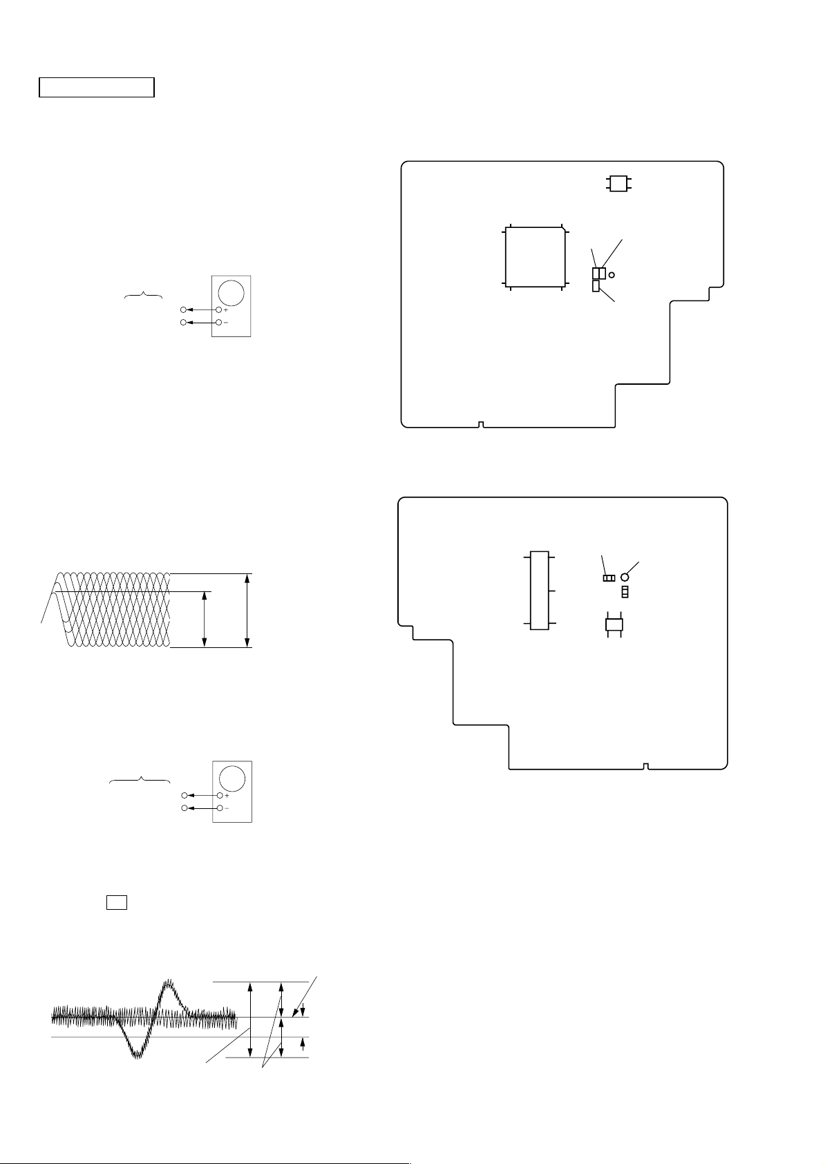
CD-R SECTION
Note :
1. CD Block is basically designed to operate without adjustment.
Therefore, check each item in order given.
2. Use YEDS-18 disc (3-702-101-01) unless otherwise indicated.
3. Use an oscilloscope with more than 10MΩ impedance.
4. Clean the object lens by an applicator with neutral detergent
when the signal level is low than specified value with the following checks.
RF Level Check
oscilloscope
BD-R board
TP(RRF)
1
IC302
Procedure :
1. Connect oscilloscope to TP (RRF) and IC302 1 pin.
2. Turned Power switch on.
3. Load a disc (YEDS-18) and playback.
4. Confirm that oscilloscope waveform is clear and check RF signal level is correct or not.
Note : Clear RF signal waveform means that the shape “ ◊ ” can be clearly
distinguished at the center of the waveform.
pin
Adjustment Location:
[BD-R BOARD] (SIDE A)
25
26
IC301
50
51
[BD-R BOARD] (SIDE B)
75
8
1
4
5
100
C363
76
IC302
R3C6
TP(RRF)
C396
1
RF signal waveform
VOLT/DIV : 200mV
TIME/DIV : 500ns
3T
3T= 0.55
11T= 0.90
11T
±
0.07Vp-p
±
0.13Vp-p
E-F Balance (1 Track jump) Check
oscilloscop
BD-R board
TP(TE1)
PN301
qk
pin
Procedure :
1. Connect oscilloscope to TP (TE1) and PN301 qk Pin.
2. Turned Power switch on.
3. Load a disc (YEDS-18) and playback the number five track.
4. Press the X button. (Becomes the 1 track jump mode.)
5. Confirm that the level B and A (DC voltage) on the oscilloscope waveform.
1 track jump waveform
center of
waveform
1
31
PN301
18
32
C380
2
TP(TE1)
R369
41
58
0V
level=1.3±0.6Vp-p
Specified level: –– × 100=less than ±22%
A
B
20
B
symmetry
A (DC voltage
Page 21

THIS NOTE IS COMMON FOR PRINTED WIRING
BOARDS AND SCHEMATIC DIAGRAMS.
(In addition to this, the necessary note is printed
in each block.)
For schematic diagrams.
Note:
• All capacitors are in µF unless otherwise noted. pF: µµF
50 WV or less are not indicated except for electrolytics
and tantalums.
• All resistors are in Ω and 1/
specified.
• % : indicates tolerance.
¢
•
• C : panel designation.
Note:
The components identified by
mark ! or dotted line with mark
! are critical for safety.
Replace only with part number
specified.
: internal component.
4
W or less unless otherwise
Les composants identifiés par
une marque
! sont critiques pour la sécurité.
Ne les remplacer que par une
piéce portant le numéro spécifié.
RCD-W3
SECTION 5
DIAGRAMS
• Signal path.
J : CD
c : CD (digital)
I : CD REC
L : CD REC (digital)
• Abbreviation
CND : Canadian model
For printed wiring boards.
Note:
• : Pattern from the side which enables seeing.
(The other layers' patterns are not indicated.)
Caution:
Pattern face side: Parts on the pattern face side seen from the
(Side B) pattern face are indicated.
Parts face side: Parts on the parts face side seen from the
(Side A) parts face are indicated.
• A : B+ Line.
• B : B– Line.
• H : adjustment for repair.
• AC voltage readings in the bias oscillator with a level
meter.
• Voltages and waveforms are dc with respect to ground
under no-signal conditions.
no mark : STOP
( ) : PLAY
< > : REC (CD-R only)
• Voltages are taken with a VOM (Input impedance 10 MΩ).
Voltage variations may be noted due to normal production tolerances.
• Waveforms are taken with a oscilloscope.
Voltage variations may be noted due to normal production tolerances.
• Circled numbers refer to waveforms.
5-1. CIRCUIT BOARDS LOCATION
BD-P board
HP board
• Indication of transistor
C
Q
These are omitted
EB
• Abbreviation
CND : Canadian model
POWER board
AUDIO
board
C
EB
These are omitted
FL board
BD-R board
VOL board
21
Page 22

RCD-W3
– BD-R SECTION –
IC301 ia (RRF IN)
1
0.2V/div
µ
sec/div
0.5
IC301 tk (FE)
2
0.1V/div
5msec/div
IC301 tj (TE)
3
0.5V/div
5msec/div
IC207 rf (34MCLK)
4
0.8 Vp-p
0.1 Vp-p
0.5 Vp-p
1.8 Vp-p
IC502 qs (ILRCK)
5
10
6
0.2
7
8
1V/div
µ
sec/div
1V/div
µ
21µsec
IC502 qd
sec/div
IC510 td (AD MCLK)
90nsec
IC510 t; (MCLK IN)
(ISCLK)
0.44µsec
3.2 Vp-p
3.2 Vp-p
3.4 Vp-p
1V/div
50nsec/div
3.3 Vp-p
IC403 qg (RF AC)
9
0.5V/div
µ
sec/div
0.5
IC403 qh (FE)
0
0.1V/div
5msec/div
IC403 ql (TE_BAL)
qa
0.5V/div
5msec/div
IC407 yh (EXTAL)
qs
1.6 Vp-p
0.1 Vp-p
0.5 Vp-p
1.5 Vp-p
IC408 2 (XOUT)
qd
1V/div
20nsec/div
IC201 (XIN)
qf
33.86MHz
IC203 yh (EXTAL)
qg
20MHz
4.9 Vp-p
33.86MHz
149
3.3 Vp-p
1V/div
20nsec/div
1.7 Vp-p
0.5V/div
20nsec/div
29nsec
1V/div
20nsec/div
– PANEL SECTION –
IC801 4 (X2)
1
5.3 Vp-p
5MHz
0.1
2V/div
µ
sec/div
33.86MHz
1V/div
20nsec/div
0.5V/div
20nsec/div
20MHz
22
Page 23

5-2. BLOCK DIAGRAMS – CD-R SECTION (1/2) –
RCD-W3
OPTICAL
PICK-UP BLOCK
(KRS-220C)
(DECK B)
LD
PD
FOCUS
COIL
TRACKING
COIL
M609
LOADING
MOTOR
(DECK B)
M301
SLED
MOTOR
(DECK B)
A
A
B
B
C
C
D
D
E
E
F
F
G
G
H
H
VWDC1
VWDC2
FPDO
VRDC
ODON
W/XR
IN3-
OSCEN
LD DRIVER/CONTROL
FPDVC
PDVC
FCS-
TRK+
TRK-
M
M
TRAY+
TRAY-
D301
1 3
7 5
IC302
BUFFER
34
35
32
31
36
37
A
9
A
10
B
5
B
6
+4V
FO+FCS+
FO-
TO+
TO-
LO+
LO-
SL1+
SL1-
SL2+
SL2-
VWDCLMT
VWDC2
FPDO
ODON
W/XR
ENBL
OSCEN
RREF2
BTL MOTOR DRIVE
IC303
DRV
DRV
DRV
DRV
DRV
BAS
Q301
FOIN+
TOIN+
LOIN+
SLIN1
SLIN2
REF
MU1
Q302
ERGCNT
27
28
40
1
2
25
41
FOCUS/TRACKING,ERROR
AIN
98
BIN
97
CIN
96
DIN
95
EIN
93
FIN
92
GIN
91
HIN
90
RREF2
6
VWDCN
7
VWD1
8
FPDO
99
VRDC
4
VRDCN
3
RREF1
5
RREF1
TAO
LDIN
SLD MOVE A
SLD MOVE B
DRV EN
RF EQUALIZER,
DETECT
IC301
S/H
MATRIX
FAO
DVC
RFO
SRFO
FEO
VC
+2V
Q303
HAVC
WREF
1027
WREF
APC
FVREF
MFPDSH
100
3128 94 32 46 15
WFPDSH
CE
RF PDSH
MLDON
RF PDSH
WLDONCEWBLSH
RREF1
VWDC2
RREF2
WREF
HAVCOFS
VWDCLMT
81
82
RRF
RRFIN
RF EQ
CEO
WBLSH
SPDSH
MPDSH
ROPCSH1
33 34 35 38 13 19
SPDSH
MPDSH
ROPCSH_E
+4V
65
MSPP
CEM
MPXOUTCSXLAT
MPXOUT
D/A CONVERTER
AO1
18
AO2
19
AO3
2
3
AO4
AO5
4
5
AO6
6
AO7
7
AO8
AO9
8
9
AO10
AO11
12
AO12
13
CE
IC304
MPX
REGISTER
TFGCNT
4148 42 43 45
/CXACS
DO
CLK
LD
63
RFRPIN
SDATA
SCLK
ERGCNT
CXADATA0
/CXACLK
ERGCNT
17
16
15
ATFG
30 47 61 6253
AGCON
WBLIN
DADATA
/DACLK
/DACS
+4V
REG.
4 2
IC210
PH/BH
FE TE
AGCON
RFCT
RFRP
+5VA
EQRFP
EQRFN
BH01
BH01
TEIN
XTOR
XTOK
RECD
SWRF
7
EFM(RFAC)
BLEVEL0
AGCON
MPXOUT
BS
RP
TE
FE
ASYM2
ASYM1
79
80
78
53
48
59
81
AMYS2
BLEVEL0
AMYS1
XTOK
RECD1
AGCON
MPXO
67
68
NC
71
72
56
TE
57
FE
58
50
51
52
88
IC306 (1/2)
21
TE AMP
BLEVELO
TEBC
+2V
COMPARATOR
IC305(2/2)
6
5
3
2
COMPARATOR
IC305 (1/2)
7
1
IC308
1
2
EFM
BS
RP
TE
FE
RX
TX
CD-R
A
SECTION
(2/2)
(Page 24)
IC307
RPBC
FLAGC
FPDO
WLDON
REPDSH
WFPDSH
WBLSH
SPDSH
MPDSH
W/XR
OSCEN
ENBL
ODON
2 1
4
NC
17MHz
1
NC
ERGCNT
14
13
WLDON
5
REPDSH
WFPDSH
3
WBLSH
6
SPDSH
7
8
MPDSH
W/XR
18
19
OSCEN
ENBL
20
21
ODON
IC207
RDPCON
CDR/RW
WR/RE
ATIP/EFM
ADTRIG
CPLD
EEPROM
IC208
32
33
34
36
38
CS
CK
DI
DO
RDPCON
/CXACS
CXADATA
/CXACLK
1
2
3
4
DADATA
/DACLK
/DACS
23
21
61
83
18
19
24
60
20
7
2
90
/CXACS
EP CS
SDATA IN
FPDO
SDATA
SCLK
/DA CS
RDPCON
CDR/RW
WR/R
ATIP/EFM
ADTRIG
SYSTEM
CONTROL
IC203 (1/2)
M401
SPINDUL
MOTOR
(DECK B)
LIMIT
SW
M
HALL
SENSOR
W
V
U
HU+
HUHV+
HVHW+
HWHH+
+5VA
EEFS
EFM1
W
12
V
U
HU+
HUHV+
HV-
HW+
HW-
HB
DRIVE
CONTROL
SPIN
FG3
26
24
SPNFG
SLD IN SW
13
14
20
21
18
19
16
17
23
DMO
IC306 (2/2)
57
BUFFER
EFM2
EFM3
ROPC1
RESAMP1
EFCK
RESAMP2
39
29
30
40
41
42
43
2
44
EEFS
EFM1
EFM2
EFM3
ROPC1
RESAMP1
EFCK
RESAMP2
34MCLK
WRSMP
MONTITO
LDON
WGATE
HRSW
/RST
WRSMP
12
MONTITO
22
LDON
23
WGATE
27
HRSW
31
/RST
16
DRV EN
SLD IN SW
SLD MOVE A
SLD MOVE B
100
DRV EN
/SLD IN SW
49
SLD MOVE A
84
SLD MOVE B
85
RESET
63
SYS BUS
34MCLK
•Signal Path
: CD PLAY
: CD REC
B
CD-R
SECTION
(2/2)
(Page 24)
23 23
Page 24

RCD-W3
– CD-R SECTION (2/2) –
A
CD-R
SECTION
(1/2)
(Page 23)
B
CD-R
SECTION
(1/2)
(Page 23)
34MCLK
SYS BUS
EFM
JK703
DIGITAL
OPTICAL
IN
163 E F M
BS
RP
TE
FE
RX
TX
WBLIN
FAO
TAO
DMD
EFM1
EFM2
EFM3
WRSMP
RESAMP1
RESAMP2
EFCK
ROPC1
LDON
SPNFG
CE
TEBC
WGATE
FEFS
ROPCSHE
RPBC
FLAGC
WRSMP
WGATE
HFSW
/RST
201 B S
203 R P
198 T E
197 F E
191 R X
192
193
8
132
207
208 T R O
3
NC
2
183 EFM1
184 EFM2
185 EFM3
180 WRSMP
181 RESAMP1
182 RESAMP2
177
186
142
7
204
194
166
179
187
202
139
180
166
167
TX
TC
C34M
WBLIN
FOO
SLO
DMD
EFCK
ROPC1
LDON
FG
CE
TEBC
WGATE
FEFS
ROPC2
RPBC
FLAGC
WRSMP
WGATE
HFSW
UAD0
96-103
I
UAD7
130-122
UA0
DSP
SERVO
IC201
URD
I
UA8
UWR
UCS0#
UCS1#
URDY
UINT0#
UINT1#
SDINT#
FLAGA
FLAGB
EFSF
HRST
104 105
106 107
110 111
112 113
137 138 87
NC
9553
PRST
DOUT
C2PO
ABCK
ALRCK
HD0
I
HD15
HWR
RD0
RD15
RA0
RAD9
ROE#
XIN
I
I
RX
146
143
144
145
85-91
72,73,76-82,
70
69HRD
56ATA CS3
57ATA CS1
60HA0
62HA1
59HA2
21-14
32,33,29-24,
45-81
52-48,
30RCASH#
31RCASL#
38RRAS#
37RWE#
36
149
+5VD
BUS DA0
BUS DA2
CSB1
CSB3
ROUT
DLRCK
DBCK
+3.3V
2-5,7-10,
18-21,
31 /UCAS
32 /LCAS
15 /RAS
14 /WE
30 /DE
ZD201
INTIAL
)
RESET
IC706(1/2)
RAM
IC202
I/O0
I
I/O15
35-38,40-43
A0
I
24-29
A9
)
WAVE
SHAPER
HD0-15
10131
RW DATA
RW LRCK
RW CLK
P DATA
P BLK
P LRCK
P DOUT
FPGA RST
FPGA AS
FPGA WD
FPGA CLK
DAC CS
FPGA CS
CXD MUTE
37 41
R OPT IN DOUT
59
RW DOUT
RW DOUT
36 66
RW DATA
65
RW LRCK
63 44
RW CLK
64
FP.GA
IC510
ATAPIL <0>
I
2-8,
ATAPIL <15>
11-19
1
ATA WR
CS1
60
P DATA
29
P CLK
27
28
P IRCK
32
P DOUT
RESET
52
FPGA AS
67
DA PDATA
26
SDATAO1
23
DA PCLK
25
SCLK1
22
DA PCS
24
FPGACS1
21
CXD MUTE
71
MCLK IN
50
CDR RST
74 53
SRC RXP
SRC DATA
SRC CLK
SRC LRCK
S D TXP
S D DATA
S D LRCK
S D CLK
OMCK
DUB START
DA RDATA
DA RCLK
DA RCS
DA DATA
DA CLK
DA LRCKL
DAC MCLK
CS DAC
SCK DAC
DASDT C
DUB SEL
DAC RST
AD DATA
MCLK IN
AD LRCK
AD MCLK
45
46
62
68
69
70
48
79
78
77
76
49
51
42
55
35
34
33
72
73
43
39
40
F DOUT
DUB START
DA RDATA
DA RCLK
DA RCS
IC706(2/2)
WAVE
SHAPER
85
TX
1
RXP
4
RXN
5
SDIN
14
ISCLK
13
ILRCK
12
TXP
26
TXN
25
NC
SDOUT
18
OLRCK
17
OSCLK
16
OMCK
21
JK705
DIGITAL
OPTICAL
OUT
RECEIVER
SERIAL
AUDIO
INPUT
DRIVER
SERIAL
AUDIO
OUTPUT
OUTPUT CLOCK
GENERATOR
DA DATA
DA CLK
DA LRCK
DA MCLK
CS DAC
SCK DAC
SDT DAC
DUB SEL
DAC RST
AD DATA
AD BCK
AD LRCK
AD MCLK
DUB SEL
CDP 33M
CLOCK&DATA
RECOVERY
AES3
S/PDIF
ENCODER
CONTROL PORT &
REGISTERS
AD0/CS
AD1/CDIN
SDA/CDOUT
1 2 27 28 19 9
SRC CS
SRC DATA
SRC DIN
C
AUDIO
SECTION
(Page 26)
DECODER
INT
SCL/CCLK
SRC INT
SRC CLK
AES3
S/PDIF
CONVERTER
RST
SRC RST
SAMPLE
RATE
DIGITAL AUDIO
SAMPLE RATE
CONVERTER
IC502
27-34
UAD0 IUAD7
36-43,45
UA0 IUA8
70 71
/URD
5458 88 89
UCS1
/UCS0
/UHWR
/WAIT(URDY)
/UNIT0
/UNIT1
93 56 178
FLAGA
FLAGB
SRC CS
DA RCS
SRC DIN
DA ROLK
DA RDATA
DUB START
94 9 6
3
DA RCS
DA RCLK
52 97 98
8 66
ESFS
/OAK RST
SYSTEM CONTROL
IC203 (2/2)
DA RDATA
DUB START
HOT RX
/SRC CS
SRC CLK
SRC DATA
99
51
SRC CLK
SRC DOUT
SRC INT
SRC RST
96
HOT TX
24 24
/SRC RST
X201
20MHz
67
XTAL
EXTAL
/LOAD_SW46/OPEN_SW
47
(LOADING) TRAY
( )
OPEN
REC TXD
REC RXD
TRK INC
FWE
MD2
BTS RXD
BTS TXD
SW201
(LOADING/OPEN)
(DECK B)
DATA BUS
12
14
16
PN105
10
75
15
13
FWEN
FWMD2
RXD
TXD
CHECK
CONNECTOR
REC TXD
REC RXD
TRK INC
D
CDP
SECTION
(Page 25)
•Signal Path
: CD PLAY
: CD (DIGITAL)
: CD REC
: OPTICAL
Page 25

– CDP SECTION –
OPTICAL
PICK-UP BLOCK
(DECK A)
RF
A
A
B
B
C
C
D
D
E
E
F
F
V.C
VCC
LD
PD
FOCUS
COIL
TRACKING
COIL
M902
SLED
MOTOR
(DECK A)
M903
LOADING
MOTOR
(DECK A)
M901
SPINDUL
MOTOR
(DECK A)
LIMIT
SW
M
M
M
HALL
LD
MD
VR
F+
F-
T+
T-
A
A
B
B
L+
L-
SENSOR
+5VA
FCS+
FCS-
TRK+
TRK-
W
V
U
HU+
HUHV+
HVHW+
HWHH+
+5VA
SLEDIN SW
LD
DRIVER
Q501
ERROR AMP
IC404
2
3
RCD-W3
DIGITAL SERVO
DIGITAL SIGNAL PROCESSOR
FOK
FOK
F
IC402
CPU
INTERFACE
DATA
XLAT
CLOCK
CXD XLAT
CXD DATA
SYSTEM
CONTROL
IC407
POW CTL
FLD TXD
FLD CLK
FLD CS
RMC IN
KEY_IN0
KEY_IN1
KEY_IN2
SCLK
SENS
SCLK
CXD CLK
D/A
PROCESSOR
32K
RAM
SENS
MUTE
MD2
GFS
GFS
CXD MD2
59
13
17
18
100
78
79
80
XTSL
CXD XTSL
PWR CTL
FL SDI
FL SCK
FL CE
REMO IN
KEY IN0
KEY IN1
KEY IN2
DIGITAL
SERIAL/
PARALEL
PROCESSOR
SQSO
SCOR
SCOR
SQSO
OUT
CLOCK
SQCK
SQCK
PCMD48
XRST
FPGA RST
FPGA DATA
FPGA CLK
FPGA CS
FPGA AS
PROG ON
DUB SEL
REC TXD
AS DATA
TRK INC
PWR MUTE
DOUT
BCK48
LRCK48
MUTE
XTLO
XTLI
MCKO
DAC CS
MD2
FW EN
XTAL
EXTAL
/RESET
SW
70
48
49
47
71
12
13
67
23
24
25
2
8
75
10
15
38
14
12
6
67
66
63
60
26
NC
NC
CLOCK
OSC
IC408
X402
20MHz
1
DRIVE
XTAL
OSC
XIN
1 2
X401
33.86MHz
IC409
RESET
P DOUT
P DATA
P BCK
P LRCK
6
FS OUT
XOUT
CXD MUTE
FPGA RST
FPGA WD
FPGA CLK
FPGA CS
DAC CS
FPGA AS
2
+5VU
PN402
MD2
FWEN
PROG DN
FL SDI
DATA BUS
CDP 33M
CONNECTOR
CHECK
DUB SEL
REC TXD
REC RXD
TRK INC
PWR MUTE
LEVEL SEL
LEVEL IN
D
E
CD-R
SECTION(2/2)
(Page 24)
AUDIO
SECTION
(Page 26)
RF AMP
IC403
EQ_IN
3
A
6
B
7
C
8
D
9
E
10
F
11
VC
27
DVC
14
LD
1
PD
2
1
FO+
34
FO-
35
TO+
32
TO-
31
SL1+
9
SL1-
10
SL2+
5
SL2-
6
LO+
36
LO-
37
W
12
V
13
U
14
HU+
21
HU-
20
HV+
19
HV-
18
HW+
17
HW-
16
HB
23
VC
APC
DRV
DRV
DRV
DRV
DRV
AC
AMP
BTL MOTOR DRIVE
IC405
MUTE
DRIVE
CONTROL
EQ
RF SUM
AMP
FOCUS
ERROR
AMP
TRACKING
ERROR
AMP
FOIN
TOIN
MU1
SL1IN
SL2IN
LOIN+
SPIN
REF
FG3
RFAC
15
RFDCO
28
RFDCI
29
FEI
17
FE
16
TE
18
CE
20
CEI
21
SWSW
12
VFC
25
VFC
SLD ERR
27
28
41
1
2
40
25
24
26
FAO
TAO
DRV_MUTE
SLDCTLA
SLDCTLB
TRAY CTL
SAO
Q402
SPNFG
MDP
SLD IN
SELECT DATA
IC406(2/2)
12
13
FAO
TAO
SAO
MDP
SPNFG
SW
SLDCTL A
SLDCTL B
TRAYCTL
SLD ERR
DRV MUTE
VFC
SLDIN
14
11
+2.7V +5VA
IC410
+2.7V
REG
RFAC
36
RFDC
23
FE
27
SE
26
TE
25
CE
24
FAO
4
TAO
3
SAO
2
VC
28
MDP
95
DATA SELECTOR
IC406(1/2)
1
2
10
AS FCS/TRK
95
FG
SW
3
84
SLDCTL A
SLDCTL B
85
TRAYCTRL
5
82
SLD ERR
DRV MUTE
9
CXA VFC
4
SLEDIN SW
90
1.35/AUD
83
7
SW REF/AUD
SPD G UP
87
(LOADING)
(LOADING/OPEN)
15
SW4M1
(DECK A)
EFM
DEMODULATOR
ANALOG
SWITCH
•
AMP
•
A/D
CONVERTER
SERVO
DSP
TE/FE
T1 RYSW
52 51
REGISTER
ERROR
CORRECTOR
COUT
89 92 85 86 87 83 82 69 57 66 73 78 79 80
9399 18
45 41 42 43 96 48 40 47 39 89 46 94 20
COUT
TRYSW2
TRAY
( )
OPEN
POWER
SECTION
(Page 27)
25 25
•Signal Path
: CD PLAY
: CD (DIGITAL)
Page 26

RCD-W3
– AUDIO SECTION –
CD-R
SECTION
(2/2)
(Page 24)
DA DATA
DA CLK
DA LRCK
DA MCLK
SDT DAC
SCK DAC
CS DAC
DAC RST
D/A CONVERTER
IC7V1
SDT1
3
BICK
2
LRCK
4
MCLK
1
8
7
6
5
AUDIO I/F
CONTROLLER
I/F
CONTROL
DAC
DAC
AOUTL+
AOUTL-
AOUTR+
AOUTR-
12
11
10
9
L-P-F
IC704
5
6
3
2
7
1
PHONES AMP
JK701
(1/2)
L
ANALOG
OUT
R
IC707
LEVEL METER SELECTOR
IC703
CH1/H
CH0/L
6
7
COM
1
A
C
5
A/D CONVERTER
BUFFER
Q709
BUFFER
Q710
AUDIO MUTE
SWITCH
Q701,702,706
MUTE
MUTE
5
Q703
3
Q704
7
MUTE
Q711
1
MUTE
Q712
VR801
PHONE
LEVEL
MAX
MIN
JK802
PHONES
IC7V2
AD DATA
AD BCK
AD LRCK
AD MCLK
PDN
13
STDO
9
SCLK
12
LRCK
10
MCLK
11
AUDIO I/F
CONTROLLER
ADC
ADC
AIN L
AIN R
2
1
AMP
IC702
1
7
3
5
JK701
(2/2)
L
ANALOG
IN
R
CDP
SECTION
(Page 25)
VR802
REC LEVEL
DUB SEL
RELAY DRIVE
Q705
LY702
•Signal Path
: CD PLAY
LEVEL IN
LEVEL SEL
E
PWR MUTE
: CD REC
26 26
Page 27

– POWER SECTION –
RCD-W3
CDP
SECTION
(Page 25)
KEY IN0
KEY IN1
KEY IN2
RMC IN
S11
FLD TXD
FLD CLK
FLD CS
F
8
SCK1
7
15
P00
FL DRIVER
F0
F15
F16
F35
G1 - 16
80
I
I
65
64
I
P1 - 20
61
I
•
58
I
43
IC801
X1
3
X801
5MHz
4
X2
60
VLOAD
6 3 1
RESET
-34V
RESET
IC802
KEY MATRIX
SW808, 5W810 - 814
FLUORESCENT
INDICATOR TUBE
FLD801
SW801 - 807
SW815 - 822
+5VU
(F1)
(F2)
RMC801
REMOTE
COMMANDER
1
RECIEVER
-34V
-8VA
+8VA
+12V
+8VA
+3.3V
+5VA
+5VM
+5VD
D104 D103
-23V
-28V
ZD101
-8V REG.
3 2
IC106
+8V REG.
3 1
IC107
+3.3V REG.
2
IC105
4
L110
PT101
POWER
TRANSFORMER
D120
D107
D108
D110
D109 D102
1
D106
2
3
DRAIN
DCP
GND
SWITCHING
REGURATOR
IC101
1
VCC
FB
4
BD101 L101
5
LINE
FILTER
F101
T1.6A
POWER
SW801
AC
IN
PWR CTL
+5VU
27 27
REG.
IC104
IC102
1
4
32
Page 28

RCD-W3
5-3.PRINTED WIRING BOARD – BD-R SECTION – • See page 21 for Circuit Board location.
1
BD–R BOARD (SIDE A)
2
3 4 5 6 7
8
9 10
A
B
C
D
E
F
G
C541
R526
R527
R528
10
14 5 1
R507
C540
C525
C539
C523
R504
IC502
20 25 28
15
R533
R534
R532
R530
C520
R5Q1
L505
IC210
PN105
R503
R535
C280
RR501
FOR
CHECK
R502
R506
R5S3
C521
23
IC202
33
34
44
R501
C522
R5T6
C501
5
1
C527
R240
16
C516
C526
C518
22
12
11
R228
1
C221
C517
R284
R285
C277
R277
R261
C208
C281
C222
61
65
70
75
80
C220
C249
C250
60
1
C209
C219
IC510
510
C251
R295
51
55
60
65
70
75
C210
50
76
414520501555
IC203
80 85
R334
R521
R519
R517
40
35
30
25
21
RR202
RR203RR204RR205RR206
R214
R215
R216
R2Q1
R2Q2
26
303595409045
100
SW201
LOADING/OPEN
(DECK B)
R515
R513
R509
RR507
25
20
15
10
R525
R522
R520
R518
R516
R514
R4Q1
C349
C348
C353
C389
C390
R392
R3A2
Q303
R3A3
ECB
R234
R233
R232
R231
R352
25
26
30
35
40
45
50
51
55 60
C377
R391
R3A5
C350
R3C8
C351
R360
R361
R362
R363
R364
R365
RR201
R211
R296
R283
R247
R250
5
1
R291
R290
R280
R281
R255
C259
R251
R249
R248
R394
R3C5
R3A4
C252
C347
R351
IC301
C368
C376
R4E7
R4E5
R4K7
C4E5
R350
C375
C346
C373
C395
R345
R359
R3C7
R4G3
R355
R370
C327
R315
5
8
C326
R314
R316
R313
R357
R354
17551070156520
100
R3A7
IC408
R335
C319
42 40
1
95
90
85
80
76
C344
C343
R373
R372
R371
R4E3
4
1
R323
35
IC303
510
R318
R317
C367
C368
C370
C363
R3A8
IC302
1
4
R301
R302
R3C6
C396
R4K6
C4E1
C4E2
C320
30
C325
C301
C4E3
R326
R324
R327
25
15 21
R303
R3K1
R325
8
5
22
R304
C305
C322
C303
R331
C307
R306
R3A9 R333
R330
R329
R328
R332
R308
R307
C308
R3D1
R3D2
C309
R3C3
R3D3
R3D4
R3D5
R3D6
C4A7
C4A4
C4A3
IC409
R4C6
R4C5
C4A2
C4A1
R4C7
R4C4
1
R4F7
C4A5
C4A0
R4C3
R4F8
R4C8
C4A8
R4C9
C412
C411
3
R432
R4F9
C415
R433
R4A8
R407
D402
C4F7
PN402
1
5
IC405
10
15
21
R4A9
X402
R426
R425
C4F8
CHECK
R4CA
R4CC
C4A9
R4C0
FOR
C495
C534
C439
C437
IC410
C456
13
R455
• Semiconductor
Location
Ref. No. Location
D402 D-7
IC202 D-2
C443
C441
R4E0
R4E8
R4E9
R440
R447
C448
R444
R403
R401
R402
30359540
R4M2
C497
R4A2
R418
C496
R4C1
26
100
90
16
45
50
51
55
60
IC407
65
70
75
76
80 85
C446
25
20
R410
15
10
5
1
R411
89
1
IC406
R437
16
R434
R435
C491
R493
R492
42
40
35
R4A1
R4A0
R499
R496
R497
R495
R498
30
25
22
R4C2
R450
C478
R485
C479
R441
R451
R413
R446
C454
C403
C450
R448
R471
C468
C469
R472
C475
R479
IC404
5
8
R484
R480
C451
BCE
C481
R470
R487
R462
R467
C471
Q501
R488
R491
R483
C453
C470
R478
R482
R461
R466
4
1
R452
R460
R465
R481
R490
C480
R469
R476
R486
R463
C464
C482
R457
R458
R475
R489
IC203 F-3
IC210 E-2
IC301 C-5
IC302 B-6
IC303 G-5
IC404 D-9
IC405 F-7
IC406 D-8
IC407 C-8
IC408 E-5
IC409 D-7
IC410 A-9
IC502 B-1
IC510 B-3
Q303 D-4
Q501 C-9
M609
LOADING
(DECK B)
H
PN302
M
28 28
Page 29

RCD-W3
1
2
3 4 5 6 7
8
9 10 11
OPTICAL PICK-UP
BLOCK
A
BD–R BOARD (SIDE B)
POWER
BOARD
(Page40)
A
(KRS–220C)
(DECK B)
AUDIO
BOARD
(Page36)
C
• Semiconductor
Location
25
R356
PN501
R358
C362
C372
R376
X401
C386
3
C374
R375
R396
L306
R353
R388
C378
R399
IC306
R397
5
4
IC307
29
C352
C388
C399
C354
4
C385
R398
C253
R404
R412
C463
C4G1
C4G2
C4G3
R416
R4F1
R4F0
C401
R421
R420
R419
R4S6
C533
R4S2
12 10 5 1
C530
C529 C531
R400
ZD401
R4S4
A
K
R4S8
C410
R427
R424
R422
R4G2
R423
R4G1
R4G0
C4A6
L507
C532
L502
PN503
C311
1
5
15
25
31
R339
R338
PN301
C336
C310 C312
L301 L302
C304
2
10
R305
20
C306
C339
30
D301
32
K
A
C338
R337
R336
11
20 15
IC304
10
15
R340
C337C335
C342
C302
C364
C340
C341
C365
R3C9
IC305
Q302
Q301
C369
85
114
R374 R377
C381
R3C1
BCEBCE
C371
C387
C457
L441
C438
100 95 90 85 80 76
1
5
10
IC402
15
20
25
26 30 35 40 45 50
R443
C444
R449
R445
C447
C445
R442
C442
75
70
65
60
55
51
C440
R405
B
C455
R456
C420
C421
L442
R453
C
R468
C465
30 25 20 16
IC403
1 5 10 15
17
PN406
R473
C472
15
R474
5
1
C474
C473
C477
R477
C476
16
OPTICAL
D
PICK-UP
BLOCK
10
(DECK A)
C422
C458
C423
R414
C402
R4L9
C4E6
R417
E
C4F6
C494
PN401
C493
L491
FL
BOARD
F
(Page38)
G
BOARD
(Page42)
BD–P
B
H
Q402
R436
R4M1
R4A3
BCE
C492
R494
20
19
15
C414
10
5
2
1
C499
PN403
22
20
10
2
C498
R4A5
R4A4
21
R4A6
R4A7
15
5
1
L304
C398
C392
PN304
1
2
5
10
12
13
C330
C333 C332 C331
C329
C328
C321
C397
C391
R322
C318
R321
C317
R320
C316
R319
C315
M401
SPINDLE
H
MOTOR
R3C2
R389
C255
R235
1
R3A1
15
R590
R390
C380
R369
1
4
IC308
85
85
C382
C384
R241
R237
R236
11
12
15
IC207
20
22
23
25 30 33
R242
C254
R4K1
R4K2
R409
R408
R238
R243
5
R244
R245
15
IC208
1
2102030
R213
44
40
34
C510
R293
R209
R210
C212
C213
C256
R268
85
14
C513
C214
C217
C285
R254
R524
C515
C514
C511
R512
C508
C507
R208
RR506 RR505RR504RR503 RR502
104
105
110
C211
120
130
140
150
156
R217
R219
R223
R259
R253
R252
C258
R260
C216
C263
R266
C264
R267
C265
R286
C266
R287
C215
R218
C290
R269
C218
R221
C291
R271
X201
R270
IC201
R220
C268
C262
R5S1
708090100 60
190180170160157
R224
R222
C270
C271
R262
C503
C504
R206
200
R225
R226
R227
A
K
C269 C261
1
3
ZD201
PN303
C245
C247
C2A1
53
1
206
C223
C260
C502
R5S2
R279
R201
R265
R5T7
52
50
40
30
20
10
R263
2
4
C207
L501
R203
C248
C246
R264
C279
R205
C201
C524
R529
R531
C244
R505
M301
SLED
MOTOR
(DECK B)
M
C202
L201
(DECK B)
R289
M
R294
R292
R288
C225
C224
Ref. No. Location
D301 D-6
IC201 E-9
IC207 F-7
IC208 G-8
IC304 D-5
IC305 D-6
IC306 D-7
IC307 E-6
IC308 D-7
IC402 B-2
IC403 C-2
Q301 C-6
Q302 C-6
Q402 G-3
ZD201 G-9
ZD401 C-4
I
29 29
Page 30

RCD-W3
5-4.SCHEMATIC DIAGRAM – BD-R SECTION (1/6) –
M401
SPINDLE
MOTOR
(DECK B)
(DECK B)
LD
PD
FOCUS
COIL
TRACKING
COIL
M301
SLED
MOTOR
(DECK B)
ALL DETECT
H
A
B
C
D
E
F
G
H
OL
TR
N
ER/CO
LD DRIV
SLEDIN SW
PN303
PN304
GND
HU+
HV+
HW+
HW-
A
B
C
D
E
F
G
H
VWDC1
DC2
VW
FPDO
VRDC
ODON
/XR
W
IN3OSCEN
FPDVC
PDVC
CFREQ
CMOD
FCS+
FCSTRK+
TRKVCC
VCC
PDVCC
FGND
PDGND
PGND
DGND
M609
LOADING
MOTOR
(DECK B)
C391
C325
0.1
4P
A
A
B
B
13P
13
W
10
V
U
H+
HU-
HV-
H-
8VM
GND
C328
470p
5
1
5VA
PN301
32P
1
FCSTRKTRK+
FCS+
5
FGND
PDGND
F
B
A
10
H
PDVCC
PDVC
G
D
15
C
E
NC
FPDVC
FPDO
20
VCC
VCC
CFREQ
CMOD
PGND
25
VRDC
DC2
VW
VWDC1
DGND
OSCEN
30
ODON
W/XR
IN3-
32
R306
680
PN302
2P
LD-
LD+
C397
10
100
25V
16V
C330
C329
470p
470p
C333
0.1
C332
0.1
C331
0.1
R333
22k
2.2
R317
2.2
R318
C307
2.2
R313
R305
0
27p
C308
R307
27p
680
2.2
R314
OSCEN
R308
47k
R3C3 0
ODON
W/XR
ENBL
FPDO
TRK+
RF6
RF2
RF1
RF8
RF7
RF4
RF3
RF5
TRAYTRAY+
FCS-
TRK-
FCS+
C306
47p
C326
2200p
M
MOTOR DRIVER
SL1IN
SL2IN
VM2(8V)
ASL2
SL2+
SL2GND
RSL1
SL1+
SL1GND
W
V
U
RSP
HWHW+
HVHV+
HUHU+
C327
2200p
IC303
63021FP
B1-2
EFM
2V
L301
µH
10
L302
µH
C310
R332
R316
15k
LDIN+
VM3(5V)
VM1(8V)
5VCC
TOIN
SPIN
C311
10
16V
R339
10k
R315
15k
OSC
MU1
BRS
LOLO+
FOFO+
GND
TO+
TO-
GND
FOIN
REF
FG
HB
R329
R330
R331
220
C309
0.1
10
C312
10
0.1
16V
R301
1.2k
C302
R338
R324
10k
2.7k
10
16V
SPNBOOST
TFGCNT
CXA ON
C336
0.1
TAO
SPNFG
R302
3.3k
C335
10
16V
C315
0.01
R319
22
C319
330p
R323
33k
R326
1.8k
C322
0.1
R328
10k
C320
0.1
R3A9
220
C301
0.1
R340
82k
C337
330p
2.2
2.2
2.2
C316
R320
VREF-
AO3
AO4
AO5
AO6
AO7
AO8
AO9
AO10
VREF+
0.01
22
C392
100
16V
C321
220
6.3V
NJM3414AV(TE2)
OUT1
IN1-
IN1+
VEE
IC304
M62352GP-75E
D/A
CONVERTER
C317
0.01
R321
22
R327
1.8k
IC302
BUFFER
GND
AO2
AO1
DO
CLK
LD
ED
AO12
AO11
VCC
SLD MOVE B
SLD MOVE A
R325
2.7k
C398
10
25V
C318
R322
R303
470
VCC
OUT2
IN2-
IN2+
C304
10
16V
C340
1
0.01
22
DRV EN
R335
18k
TRAY-
TRAY+
FCS-
FCS+
TRK+
TRK-
/SLD IN SW
C303
0.1
R304
C305
10k
0.1
FPDO
R337
22k
C339
0.1
C338
R336
150p
10k
DADATAO
/DACLK
/DACS
D301
KDS121
Q301
DTC144EKA
SWITCH
L304
µH
10
L306
µH
10
R3D1
R3D2
0
D
4V
GN
FAO
C396
7p
C362
C341
0.1
10
16V
C342
0.1
Q302
DTC144EKA
SWITCH
R3D3
R3D4
0
0
0
RF
BLEVEL0
R3D5
0
ASYM2
ASYM1
C343
0.15
R356
TX
R374
270k
R369
TE
TEBC
FE
R368
0
R370
RP
R371
R372
BS
R3A7 0
R3A8 0
C368
1000p
C367
1000p
1000p
C365
1000p
C364
330p
C363
R3C6
3.3k
R3K1
2k
R3C9 0
RF8
RF7
RF6
RF5
RF4
RF3
RF2
RF1
FPDO
R354
330k
10k
R357
470
C344
C346
150p
150p
R3D6
0
R3C1
22k
IC305
NJM2903V(TE2)
COMPARATOR
OUT1
VCC
OUT2
IN1-
IN2-
IN1+
IN2+
VEE
R377
4.7k
0
0
0
0
R373
C370
R359
0
C369
220p
100p
PHC1
BHC3
BETAOUT
PHC2
BHC2
RRFIN
RRF
SRFO
SRADO
WRF
MPP
AVCC
RF
SW
GND
HIN
GIN
FIN
EIN
HAVC
DIN
CIN
BIN
AIN
FPDO
EVREF
R358
10k
1k
BHC1
SRDC
RECD10
DC
SW
TC
LDLM
VRDCN
BHO1
VRDC
C371
100p
O1
BH
RREF1
C372
BHO2
RREF2
0.1
PHO2
DCN
VW
C395
1000p
GND
EQRFP
EQRFN
FOCUS/TRACKING
ERROR DETECT
DC
REF
APCCSW
W
VW
C345
0.015
1M
R355
R376
R389
33k
3C7
R
C373
SPP
M
IC301
CXA3558R
RF EQ,
CEP
68k
R350
R353
R375
4.7k
VCC
GND
10k
R398
R397
270k
22k
0.047
68k
22k
RFRPIN
CEM
0.1
C347
RFRP
VCC
C375
0.33
RFCT
CEO
C381
0.1
C384
0.1
R396
15k
C380
150p
R3C2
33k
R390
R399
10k
15k
R388
C374
33k
0.33
R391
C376
1500p
C377
1500p
FE
TE
CS
TEIN
FCTC1
TOK1C
TOK2C
RFCTC2
R
PXOUT
ATFM
M
AGC2C
AGC3C
VTIREF
AGC1C
AUX
BGIREF
0.033
0.033
0.033
27k
27k
C350
C348
C349
R352
R351
C399
1500p
22k
C387
0.001
C378
100p
XTOK
RECD
ROPCSH1
VCT2
CAV CNT
0.1
C351
ERGCNT
SUBGND
RFPDSH
MFPDSH
DSPVCC
TC7W08FU(TE12R)
XTOR
XTAND
TFGCNT
AGCON
MLDON
DGND
SCLK
SDATA
XLAT
DVCC
VCC
GND
MPDSH
SPDSH
WBLSH
ATFG
VC
DVC
VCT1
C388
10
16V
IC308
AND
R3C8
0
OUT1
IN1-
IN1+
VEE
IC306
NJM3404AV
BUFFER
C353
0.33
C389
0.1
VCC
OUT2
IN2-
IN2+
C385
IC307
0.1
NC7SZ66P5X
AND
I/O
VCC
O/I
CTL
GND
R3A4
Q303
DTC144EKA
ITCH
SW
C386
12k
R3A5
10k
C354
0.1
10
16V
C352
100
16V
R3A3
R3A2
3.9k
15k
R3A1
0
C382
0.1
RECD1
680
R363
R394
680
R364
XTOK
R3C5
0
AGCON
WLDON
0
/CXACLK
CXADATAO
/CXACS
MPDSH
SPDSH
WBLSH
RFPDSH
R360
100
680
R365
MPXO
R392
0
680
680
R362
R361
C390
0.1
SPNBOOST
TFGCNT
ROPCSH E
WBLIN
FLAGC
RPBC
DMO
CXA ON
RX
B1-3
FPDSH
W
CE
30 30
Page 31

5-5.SCHEMATIC DIAGRAM – BD-R SECTION (2/6) –
HD
3.3V
B2-4
D OUT
/OAK RST
R293
RR202
220
10k
UAD7
UAD6
UAD5
UAD4
UAD3
UAD2
UAD1
UAD0
220
RR201
0
R209
10k
R208
/HD 7
/HD 8
/HD 6
/HD 9
/HD 5
C210
/HD 10
RCD-W3
R
/ATA W
/ATA RD
C208
R206
0.1
10k
C251
/HD 3
C209
0.1
0.1
/HD 2
/HD 1
/HD 13
/HD 14
/HD 0
/HD 15
/HD 12
0.1
/HD 4
/HD 11
ATA A1
ATA A0
ATA A2
C207
0.1
/ATA CS1
/ATA CS3
R205
CDR RST
10k
CDP 33M
B1-2
C279
10
16V
R285
4.7k
C2A1
10
16V
DAN202U
IC202
GM71VS18163CLT-6
RAM
VCC
I/O0
I/O1
I/O2
I/O3
VCC
I/O4
I/O5
I/O6
I/O7
NC
NC
NC
/WE
/RAS
NC
NC
A0
A1
A2
A3
VCC
R284
100
ZD201
VSS
I/O15
I/O14
I/O13
I/O12
VSS
I/O11
I/O10
I/O9
I/O8
/LCAS
/UCAS
VSS
RD15
RD14
RD13
RD12
RD11
RD10
RD9
NC
NC
/OE
A9
A8
A7
A6
A5
A4
RCAS0B
RCAS1B
ROEB
5VD
5VA
RD8
RA9
RA8
RA7
RA6
RA5
RA4
RR203
220
/URD
/UWR
/UCS0
/UCS1
C211
0.1
C212
0.1
EFM
2V
220
RR205
220
RR206
URDY
/UINT0
/UINT1
UA8
UA7
UA6
UA5
UA4
UA3
UA2
UA1
UA0
WBLIN
MONITO
FLAGA
FLAGB
FLAGC
LDON
ROUT
DLRCK
DBCK
C213
0.1
R211
220
RR204
220
R210
220
R213
0
UWR#
UCS0#
UCS1#
VDD
VSS
URDY
UNIT0#
UNIT1#
SDINT#
UALE
UA15
UA14
UA13
UA12
UA11
UA10
UA9
UA8
UA7
UA6
UA5
UA4
UA3
UA2
UA1
UA0
ARST#
WBLIN
MONITO
VDD
VSS
MONIT
FLAGA
FLAGB
FLAGC
FLAGD
CLKOUT
LDON
C2PO
ABCK
ALRCK
DOUT
ADATA
XOUT
XIN
AVSS
L OUT
AVDD
AVDD
R OUT
AVSS
AVSS
C215
URD
UAD7
UAD5
UAD6
UAD3
UAD4
R2
R1
AVDD
AVDD
EFM
EFMR3
EFM
ASY
1k
5.6k
15k
R216
R215
R214
C217
4700p
C216
1000p
0.1
UAD2
EFM
UAD1
VREF
UAD0
AVSS
GATE
W
PRST
GATE
W
C214
HFSW
0.1
VSS
CPUTYPE
PANICIN
HFSW
R2Q1
100
R2Q2
100
HD7
VDD
NT2
EFM
EFMNT1
HD8
EFMNT3
C218
0.1
HD6
EFMNT4
VSS
HD5
HD9
HD4
HD3
VDD
HD10
HD11
IC201
OT1-9790CE
SERVO
E1T1P
E11TS
180
R217
EFCK
EFCK
ESFS
ESFS
220
R218
EEFS
EEFS
220
R219
P
RSM
W
RSMP
W
220
R220
RESAMP1
VSS
VDD
HD2
HD12
DSP
P2
RESMP1
RESM
220
R221
RESAMP2
220
R222
HD13
1
EFM
220
R223
HD1
EFM2
220
R224
HD14
EFM3
VSS
ROPC1
220
R225
ROPC1
HD0
VDD
ROPC2
ROPC3
220
R226
ROPCSH E
C219
0.1
HD15
VDD
HDRQ
VSS
R
HRD
HW
IORDY
RX
TX
TC
R227
0
TX
RX
TEBC
DAMCK
TEBC
VSS
AVSS
HIRQ
VREF
FE
IOCS16
FE
TE
C220
0.01
HA1
HA2
HA0
VSS
VDD
HPDIAG
TE
AVSS
AVDD
BS
C223
0.1
BS
R228
VDD
HRST
CS3FX
CS1FX
HDASP
RAD0
RAD1
RAD2
RAD3
RAD4
VSS
VDD
RAD5
RAD6
RAD7
RAD8
RAD9
RAD10
RAD11
RRAS#
RWE#
ROE#
VSS
VDD
RD1
RD0
RCASL#
RCASH#
RD8
RD9
RD10
RD11
RD12
RD13
VSS
VDD
RD14
RD15
RD2
RD3
RD4
RD5
RD6
RD7
SBRK
MON
VSS
VDD
VDD5
C34M
FG
REVDET
TEST1
TEST0
SLO
DMO
AVSS
TRO
RPBC
33k
C245
FOO
CE
RP
AVDD
2VREF
CE
RP
FAO
RPBC
0.1
3300p
C221
0.1
C222
R279
R201
47k
C201
16V
10
0
C244
0.0015
ROEB
RCAS0B
RCAS1B
DMO
RD10
RD11
RD12
RD13
RD14
RD15
RA0
RA1
RA2
RA3
RA4
RA5
RA6
RA7
RA8
RA9
RD1
RD0
RD8
RD9
RD2
RD3
RD4
RD5
RD6
RD7
L201
10µH
R203
220
C202
10p
34MCLK
C247
RD0
RD1
RD2
RD3
RD4
RD5
RD6
RD7
RA0
RA1
RA2
RA3
C249
C250
0.1
IC210
BA3939-E2
+4V REG
CTRL
IN
C248
10
16V
C281
0.1
C280
0.1
OUT
GND
NC
C246
10
16V
0.1
R240
4.7k
0.1
B4
B2-3
EFM 1
EFM 2
EFM 3
/RESET
4V
TAO
GND
SPNFG
31 31
Page 32

RCD-W3
5-6.SCHEMATIC DIAGRAM – BD-R SECTION (3/6) – • See page 43, 45 for IC Pin Function Description.
B3-6
B3-4
SPNFG
GND
TAO
4V
FWMD2
5VD
C256
0.1
C255
0.1
C254
0.1
C253
10
16V
WRSMP
WLDON
W/XR
OSCEN
ENBL
ODON
R231
330
R234
R233
R232
FPDO
SLD MOVE B
SLD MOVE A
10k
R266
FPDO
SLDMOVE B
SLDMOVE A
UA7
UA5
UA6
UA7
UA5
UA6
MPXO
ASYM2
BLEVEL0
1k
1k
4.7k
4.7k
R269
R287
R286
R267
MPXO
ASYM2
BLEVEL0
SLD ERR
A DATA ZERO(JIG DOWN)
UA8
/LOAD SW
/OPEN SW
VSS
UA8
ASYM1
1k
R270
ASYM1
RECD1
RECD1
/SLD IN SW
AVCC
VREF(4V)
MD2
MD1
MD0
/LWR
/UWR
/URD
XTAL
EXTAL
/RESET
/STBY
SDATA IN
ROPCON
AGCON
/WAIT(URDY)
FLAGB
OPTION 1
TP(IN)
XTOK
HOT RX
HOT TX
/SLD IN SW
R295
4.7k
VCC
VSS
NMI
VSS
C290
C266
C265
C264
C263
C268
C291
C262
/AS
C277
0.1
0.047
0.047
0.01
0.015
0.01
0.1
0.047
0.1
C269
16V
C261
16V
10
10
R277
10k
/UWR
/URD
X201
20MHz
C271
15p
C270
15p
SDATA IN
ROPCON
4.7k
AGCON
URDY
FLAGB
XTOK
SRC DIN
SRC INT
SW201
(LOADING/OPEN)
(DECK B)
R292
10k
R294
10k
C225
0.01
R288
470
C224
0.01
R271
R289
470
FLAGA
SRC CS
DRV EN
SRC CLK
SRC RST
SRC DATA
DUB START
PN105
FWMD2
FWEN
FOR
CHECK
220
R237
220
R236
0
R235
330
220
220
C252
0.01
MONITO
RXD
TXD
DGND
5VD
B1-3
WFPDSH
WRSMP
WLDON
ERGCNT
VCC
/RST
GND
W/XR
OSCEN
ENBLE
ODON
MONITO
LDON
TCK
LDON
TMS
TDO
C260
TDI
GND
0.1
MPDSH
220
R241
MPDSH
VCC
WBLSH
SPDSH
220
220
R243
R242
SPDSH
IC207
CST0100C
CPLD
WGATE
WGATE
0
R238
RFPDSH
220
R244
WBLSH
RFPDSH
EFM1
HFM ON
220
R245
GND
EFM2
HFSW
WFPDSH
RESMAP2
ROPCON
HFSW
VCC
47
R254
17MHZ
CDR/RW
R261
R262
R263
R264
C285
0.1
CS
47
R253
34MCLK
EFCK
RESMAP1
ROPC1
EFM3
EEFS
ADTRIG
WBLOCK
ATIP/EFM
VCC
WR/RE
100
100
100
100
NC
SK
47
R252
ORG
DI
FWMD2
BTS RXD
BTS TXD
R265
4.7k
GND
CAT93C86S-LE10
DO
47
R248
47
R250
47
R249
47
R247
IC208
EEP ROM
CXADATAO
RESAMP1
R268
SDATA IN
DADATAO
/DACLK
/CXACLK
RESAMP2
34MCLK
EFCK
ROPC1
EEFS
220
ATIP/EFM
WR/RE
CDR/RW
ROPCON
R260
100k
ATIP/EFM
DA RCS
/UCS1
/UCS0
DA RCLK
WR/RE
/OAK RST
DA RDATA
REC TXD
BTS TXD
REC RXD
BTS RXD
TRK INC
CDR/RW
/CXACS
/DACS
C258
100p
R283
R251
R255
R281
R280
R259
47
47
47
47
R290
DRV EN
SRC CLK
TP(I/O)
UAD0
UAD0
R291
SRC DOUT
UAD1
UAD2
UAD2
UAD1
/SRC CS
/SRC RST
UAD3
UAD3
SPINFG
UAD4
UAD4
FLAGA
DUB START
UAD5
UAD6
UAD6
UAD5
VSS
UAD7
UAD7
C259
0.1
VCL
47
47
47
150
R296
ATIP/EFM
/DA RCS
/UCS1
/UCS0
DA RCLK
WR/RE
/OAK RST
DA RDATA
FWE
VSS
REC TXD
BTS TXD
REC RXD
BTS RXD
TRK INC
/SDINT
SDATDA OUT
SCLK
CDR/RW
EP CS
VSS
/CXA CS
/DA CS
TP(I/O)
10k
ESFS
/UINT1
/UINT0
ESFS
AVSS
/UINT0
/UINT1
ADTRIG
OPTION 2
IC203
HD64F3062BFBL-W3CDR
SYSTEM
CONTROL
UA3
UA4
UA1
UA2
UA0
VCC
UA3
UA4
UA1
UA2
UA0
/RESET
EFM 1
EFM 2
B4
EFM 3
B2-3
32 32
Page 33

5-7.SCHEMATIC DIAGRAM – BD-R SECTION (4/6) –
RCD-W3
D OUT
B2-4
CDP 33M
3.3V
SDA/CDOUT
AD0/CS
PH
EM
RXP
RXN
VA+
AGND
FILT
RST
CK
RM
RERR
CK
ILR
ISCLK
SDIN
DA XCK
FPGACS 1
IC502
CS8420-CSR
SRC
C521
0.1
DA RCLK
DA RDATA
DUB START
DA RDATA
DUB START
SCLK 1
SDATAO 1
100
100
R408
R409
SCL/CCLK
AD1/CDIN
SDOUT
OLRCK
OSCLK
DA RCS
DA RCS
DA RCLK
DA PCS
DA PCLK
R4K2 100
TXP
TXN
H/S
VD+
DGND
CK
OM
U
INT
TCBL
532
R
R533
DAC RST
R5S2 0
R5T6 0
CDR RST
DUB TRK INC
DA PDATA
P CLK
R4K1 100
220
220
DUB SEL
DAC RST
VC0IS05
P IRCK
P DATA
R5T7 0
CXD MUTE
IC510
FPGA
VCC
S D CLK
S D LRCK
P DOUT
GND
R534
FPGA AS
S D DATA
DASDT C
0
0
R513
R514
RXP
RW DATA
FPGA AS
SRC RXP
SCK DAC
CS DAC
0
R515
220
RW CLK
RW CLK
RW DATA
RW DOUT
R OPT IN
330
R535
RW LRCK
S D TXP
RW LRCK
DIG ON
MCLK IN
0
R516
OMCK
AD LRCK
0
R517
R531
R529
R530
330
R5Q1 100
R5S3 0
RW
TEST M
DAC M
AD M
M
DA DATA
SRC LRCK
SRC CLK
SRC DATA
AD DATA
DA LRCKL
330
330
C520
0.1
CS 1
DOUT
ODE
GND
RESET
DA CLK
CLK IN
GND
VCC
DOUT
CLK
CLK
F75
SRC CLK
SRC DATA
L501
µH
10
SRC INT
CS1
DOUT
RW
0
R5S1
NC
AD M
SW
SW
AD DATA
0
R518
CLK IN
M
SW
0
R519
CLK
LRCK
BCK
DATA
0
R521
0
R520
0
R522
R524
10k
C534
0.1
C518
0.1
C517
0.1
C516
0.1
C515
0.1
C514
C513
0.1
0.1
PN503
12P
C533
100
16V
8V
PWR CTL
PWR CTL
CXD M
FPGA RST
3.3V
UTE
5VA
C532
0.1
C531
6.3V
AGND
100
GND
5VD/M
L507
10
-28V
GND
-23V
-34V
5VU
µH
-28V
-23V
-34V
L502
0
C529
100
6.3V
C530
0.1
DIG IN
OPT IN
AD DATA
AD BCK
AD LRCK
CLK
AD M
DA CLK
DA DATA
DA LRCK
CLK
DA M
R590
0
F DOUT
CS DAC
SCK DAC
SDT DAC
DUB SEL
UTE
R M
PW
C
EXT RM
DAC RST
LEVEL SEL
LEVEL IN
R525
5VD
8V
8VM
5VA
GND
5VA
B3-4
5VU
GND
PN501
30P
30
GND
DIG IN
OPT IN
FR DIG IN
GND
25
AD DATA
AD BCK
AD LRCK
0
20
15
10
5
1
GND
AD M
GND
DA CLK
DA DATA
DA LRCK
GND
DA M
A DATA ZW
F DOUT
CS DAC
SCK DAC
SDT DAC
GND
DUB SEL
R M
PW
EXT RM
DAC RST
LEVEL SEL
LEVEL IN
GND
GND
3.3V
B4-5
CLK
CLK
UTE
C
RO
C524
10
16V
SRC DIN
RXP
RR501
220
220
220
220
220
220
RW DATA
RW DOUT
SRC CS
507
R
SRC RST
RW CLK
RW LRCK
C523
C539
5.1k
SW BCK
SW LRCK
CS1
SW DATA
C525
0.1
C541
0.1
RST
CDR
/ATA CS3
ATA A2
ATA A1
ATA A0
/ATA CS1
/ATA RD
/ATA W
HD
DBCK
DLRCK
ROUT
R509
/HD 15
/HD 0
/HD 14
/HD 1
/HD 13
/HD 2
/HD 12
/HD 3
/HD 11
/HD 4
/HD 10
/HD 5
/HD 9
/HD 6
/HD 8
/HD 7
R
RR507
0
RR502
RR503
RR504
RR505
RR506
220
0.01
0.01
C501
R501
220
R502
220
R503
47k
R504
1k
8200p
C540
505
330
R
R506
100
R528
100
527
R
100
R526
100
C502
C526
100
1
L505
10
0.1
6.3V
µH
C527
0.1
R
ATA W
ATAPIL<15>
ATAPIL<0>
ATAPIL<14>
ATAPIL<1>
ATAPIL<13>
ATAPIL<2>
ATAPIL<12>
GND
VCC
ATAPIL<3>
ATAPIL<11>
ATAPIL<4>
ATAPIL<10>
ATAPIL<5>
ATAPIL<9>
ATAPIL<6>
ATAPIL<8>
ATAPIL<7>
GND
INT
C522
0.1
MCLK IN
C503
0.1
C504
0.1
C507
0.1
R512
4.7k
C508
0.1
FPGA CLK
FPGA CS
DAC CS
FPGA WD
P BCK
P LRCK
P DATA
C510
0.1
P DOUT
SDT DAC
C511
0.1
SCK DAC
CS DAC
RW DOUT
DIG IN
AD LRCK
AD BCK
OPT IN
33 33
F DOUT
DA LRCK
DA CLK
DA DATA
AS PROG
DA MCLK
5VM
B4-6
Page 34

RCD-W3
5-8.SCHEMATIC DIAGRAM – BD-R SECTION (5/6) –
5VD
R FAIL
PW
SLD ERR
(DECK A)
PN406
17P
VR
M
VCC
GND
F/T
M
SAO
TAO
FAO
5VA
RF
D
LD
A
D
B
C
E
F
VC
F-
T-
T+
F+
R490
3.3k
T+
T-
R491
3.3k
DP
R477
22
R475
0
17
15
10
5
FTT+
F+
1
R478
R489
C482
3.3k
0.047
R488
3.3k
R479
68
68
Q501
2SA1162
C473
0.1
C472
0.1
C474
0.1
R476
C480
R486
0.1
8.2k
R487
C481
8.2k
0.1
C476
10
16V
C475
0.1
0
12k
R474
12k
R473
10k
R472
C471
1
C458
10
16V
C470
1
C464
0.1
IC404
NJM2100
ERROR AMP
C469
3300p
C465
16V
47
CXA2581N
LD
PD
EQ_IN
AC_SUM
GND
A
B
C
D
E
F
SW
DVCC
DVC
RFAC
IC403
RF AMP
DC_OFST
RFDCI
RFDCO
TE_BAL
RFC
VFC
BST
RFG
VCC
CEI
R463
R465
R466
R467
VC
CE
TE
FEI
FE
R485
68k
2.2k
3.3k
10k
10k
C478
0.1
3.3k
R468
R471
68k
R484
100k
R469
180k
R470
C477
16V
10
C468
120p
0
R482
R448
R483
10k
10k
0
R457
R458
R460
R461
R462
L441
10
10
µH
L442
µH
10k
82k
10k
6.8k
10k
R481
3.3k
R480
2.2k
IC410
RN5R27CA
2.7V REG
OUT
IN
GND
C479
0.1
C457
16V
XTU
R456
C455
22k
0.033
TEST
SSTP
PWMI
TMODE
AVSS
SAO
TAO
FAO
BSSD
AVD6
AVS3
M2N
PW
M2P
PW
AVD3
AVD4
XTLO
XTLI
AVS4
AVS5
PWM1P
PWM1N
AVD5
AVD2
IGEN
AVS2
ADIO
RFDC
CE
TE
C445
R446
0.01
VPCO
VC
SE
FE
330k
3.3k
R445
R450
6.8k
C451
R449
1
33k
R455
150p
C420
150p
C421
33k
R453
100k
R452
6.8k
R451
0
C450
1
C454
1200p
R447
C448
C447
R444
C446
C453
1000p
1M
0.1
0.047
10k
150p
10
LOCK
VCTL
MDP
FILO
VSC5
FILI
VDC2
PCO
3.3k
R443
C456
0.1
FOK
FOK
DFCT
AVS1
CTLV
COUT
CXD CLOK
COUT
MIRR
VDIO2
IC402
CXD3023
DIGITAL SERVO,
DIGITAL SIGNAL
PROCESSOR
ASYI
BIAS
RFAC
10k
220p
R441
33k
C444
R442
CLOK
ASYO
CXD XLAT
CXD DATA
XLAT
DATA
AVD1
AVD0
100k
R440
ATSK
VSC0
C441
C443
C442
SCLK
0.01
0.47
SCLK
ASYE
1
C463
SENS
SENS
LRCKI
10
16V
FPGA RST
VSC4
XRST
BCKI
PCMDI
SQCK
SQCK
LRCK48
SQSO
SQSO
PCMD48
C438
0.1
EXCK
BCK48
SBSO
VSC1
VSC3
VDC1
SCOR
W
M
DOUT
MCK0
XTSL
VDIO1
VSC2
MNT0
M
M
MNT3
XRAOF
C2PO
XPCK
LRCK64
BCK64
PCM
W
VDIO0
M
C4M
DCK
C437
0.1
MD2
EN
FW
PROG DN
FL SDI
SCOR
FCK
UTE
D2
NT1
NT2
GFS
D64
100
R4E8
100
R4E9
100
R4E0
CXD MUTE
P DOUT
CXD MD2
CXD XTSL
GFS
P BCK
P DATA
P LRCK
R4Q1
100
C440
0.1
C439
0.1
-28V
-34V
-23V
FL CE
REMO IN
KEY IN2
KEY IN0
FL SDI
FL SCK
RESET
KEY IN1
C423
0.001
R4M1 100k
C414
0.1
R432
C422
0.001
R433
R437
R436
R435
R434
C415
0
VCC 3.3V
B5-6
PN402
6P
33
MD2
33
EN
FW
33
PROG DN
33
FL SDI
GND
5VU
0.1
0
PN401
20P
20
F2
F2
-34V
-34V
F1
15
F1
GND
GND
5VU
FLD CS
10
RM
KEY IN 2
GND
KEY IN 0
FLD RXD
5
FLD CLK
RESET
KEY IN 1
GND
GND
1
5VU
GND
B4-5
3.3V
FOR CHECK
C IN
FE
SW
TE
VFC
34 34
Page 35

5-9.SCHEMATIC DIAGRAM – BD-R SECTION (6/6) – • See page 46 for IC Pin Function Description.
F/T
SAO
R4A5
PCL SW
O
PC
O
L+
L-
L SW
R4A6
470
1
2
R4A7
470
C499
C498
0.01
0.01
R4A4
10k
10k
C4A9
4700p
C4A8
4700p
4CC
R
10k
A
R4C
15k
4C9
R
10k
R4C8
15k
RCD-W3
B5-6
4E7
IC408
FS781BZB
OS
CK
CLO
XIN
VCC
UT
C4E3
0.01
R4E3
3.3k
XO
S1
FSOU
LF
VSS
5VA
MDP
SLD ERR
PWR FAIL
X401
33.86M
C4E2
10p
C4E1
Hz
10p
R4K6
0
TAO
FAO
4K7
R
C
0
S0
T
R
33
4E5
4G3
R
R
0
0
4F7
R
10k
4E5
C
0.1
C4F6
220
6.3V
IC409
XC61CN3002
R
T
OU
G
ESET
R4F9
27k
IN
ND
R4F8
C4F7
82k
XTU
D402
S187
KD
C4F8
1
1
VCC 3.3V
CDP 33M
5VU
GND
B4-6
5VM
OPCL SW
OPCL SW
HW
SLEDIN SW
PN403
22P
LL+
/A
/B
GND
HV+
HW
HU-
HU+
H+
H-
HV-
GND
W
SL1IN
SL2IN
VM
ASL2
SL2+
SL2GND
RSL1
SL1+
SL1GND
W
V
U
RSP
HW
HW
HVHV+
HUHU+
C496
2(8V)
0.1
+
IC405
63021FP
M
OTOR DRIVER
M
R4C0
R4A9
R4A8
R4C3
OSC
U1
M
LDIN+
3(5V)
VM
BRS
LO-
LO+
FO
FO+
GND
TO+
TO-
5VCC
GND
TOIN
FOIN
SPIN
REF
FG
HB
1(8V)
VM
2.2
2.2
2.2
2.2
IC406
BU4053BCFV-E2
DATA SELECT
Y1
Y0
Z1
Z
Z0
INHIB
VEE
VSS
C491
330p
R493
100k
C495
0.1
R4M
2 22k
R4A2 470
FF+
T+
T-
R4A1 10k
R495
10k
R4A0
18k
C497
8200p
494
R
10k
-
C494
100
16V
VCC
Y
X
X1
X0
CTLX
CTLY
CTLZ
2.2
2.2
2.2
C4A3
C4A5
C4A2
C4A0
C4A1
220
R4C4
R4C5
C4A4
470p
R4C6
470p
2.2
R4C7
470p
0.1
0.1
0.1
FE
TE
SW
VFC
C4A7
8V
22
20
OPCL SW
1
OPCL SW
2
A
15
B
+
10
5
V
U
1
0.1
C4A6
100
16V
B
/B
A
/A
W
V
U
-
HW
+
HW
HVHV+
HUHU+
H-
R4C2
H+
L-
L+
1
2
A
/A
/B
B
HV+
-
HW
+
HW
HU-
HU+
H+
H-
HV-
V
W
U
R492
R499
10k
Q402
KTD1304S
ITCH
SW
0
C492
L491
C493
220
6.3V
0.1
R496
27k
R497
4.7k
R498
22k
R4A3
10k
LEVEL IN
D2
M
KEY IN0
KEY IN1
KEY IN2
SCOR
COUT
SQCK
SCLK
AS PROG
O IN
REM
EXT RM
C
R4G2 18k
R4G1 18k
R4G0 18k
R4C1 220
R4L9 0
R421
R420
R419
R418
R417
R416
C4G1 1000p
C4G2 1000p
0
0
0
0
100
100
C4G3 1000p
C404
0.1
R413
0
5VA
VREF(4V)
KEY IN0
KEY IN1
KEY IN2
TE/FE
SLD ERR
1.35/AUD
SLD CTL A
SLD CTL B
AGND
SPD G UP
SCOR
SLDIN SW
GND
COUT
SQCK
FG
SCLK
AS PROG
AS FCS/TRK
O IN
REM
R414
100
C402
0.1
4.7k
R422
MD2
VCL
C410
0.1
4.7k
R423
MD1
DAC CS
DAC CS
R411
10k
C403
1
4.7k
R424
MD0
SW
CXA VFC
TRAYCTRL
DZ401
DAN202K
C412
15p
C411
15p
X402
20M
TRK INC
SW REF/AUD
R412
100k
TRK INC
R425
4.7k
Hz
5V
XTAL
EXTAL
HD64F3062BFBL-W
FPGA AS
FW EN
DRV MUTE
FPGA AS
FW EN
GND
PWR FAIL IN
IC407
SYSTEM
TROL
CON
GND
AS DATA
REC RXD
FL SDI
R4F0
/RESET
FL SDI
R427
R426
/STBY
3CDP
REC TXD
PROG DN
PROG DN
100
R4F3
PWR CTL
PWR MUTE
0
100
PWR MUTE
AS CLK
FL SCK
FL SCK
10k
PWR CTL
FL CE
FL CE
GND
FPGA RST
FPGA RST
0
0
R4S8
R4S6
OPTION 3
OPTION 2
GND
100
R410
FPGA RST
0
R4S4
T1RYSW
OPTION 1
FPGA DATA
FPGA CLK
FPGA WD
FPGA CLK
C4E6
1000p
TRYSW2
FPGA CS
R407
FPGA CS
R4F1
100
JIG DOW
OPTION 4
SENS
SQSO
G
CXD CLOK
CXD XLAT
CXD DATA
CXD M
CXD XTSL
DUB SEL
RESET
AUD LR
100
R400
4.7k
N
GFS
K
FO
ND
D2
5V
SW
R4F2
10k
R4S2
REC TXD
R401
R402
R403
R404
R405
0
SENS
GFS
SQSO
FOK
100
CXD CLOK
100
CXD XLAT
100
CXD DATA
100
100
CXD M
CXD XTSL
DUB SEL
LEVEL SEL
RESET
C401
D2
0.1
B3-6
35 35
Page 36

RCD-W3
5-10.PRINTED WIRING BOARD – AUDIO SECTION – • See page 21 for Circuit Board location.
A
B
C
D
1
C
BD–R
BOARD
(Page29)
1
5
15
25
29
CN701
2
10
20
30
R788
C704
2
R797
R768
R763
C725
C763
1
4
IC703
R764
R790
R70B
R70C
R70D
R70E
R70F
R70G
R70A
R779
C722
R782
R789
8
5
C708
R791
R784
R786
1
8
R778
C797
R742
5
8
IC7V1
R771
IC704
R706
5
8
16
9
C707
4
1
IC707
C778
C773
4
1
3 4 5 6 7
AUDIO BOARD (SIDE B) AUDIO BOARD (SIDE A)
C70C
C70B
C756
R776
R702
R707
R775
R772
R701
C703
C791
R796
R781
R783
R777
R795
R794
R774
R785
R798
R799
R773
R752
R750
R749
R766
R753
1
7
C757
IC706
R740
14
8
R735
R745
R746
R737
C737
C739
C758
R736
R743
C742
R738
C740
R744
OUT
DIGITAL
(OPTICAL)
IN
JK705
JK703
CN704
1
3
1
3
Q711
Q712
Q701
B C E
Q702
B C E
B C E
B C E
C744
1
3
C770
B C E
C717
1
Q706
C723
C762
G
58
PN703
C702
C761
POWER
BOARD
(Page40)
C710
C711
C771
C712
B C E
B C E
C764
Q710
Q709
C701
8
• Semiconductor
Location
Ref. No. Location
IC702 F-2
IC703 E-2
IC704 C-2
IC706 C-3
IC707 D-3
IC7V1 B-2
IC7V2 E-2
JK703 D-5
JK705 C-5
Q701 D-6
Q702 E-6
Q703 E-6
Q704 F-6
Q705 F-8
Q706 E-6
Q709 D-7
Q710 D-7
Q711 C-6
Q712 C-6
E
HP
BOARD
(Page38)
E
R741
R770
R720
R719
R733
C767
R734
C746
L703
C732
C730
L704
JK701
OUT
ANALOG
IN
LR
Q703
B C E
C728
Q704
B C E
C787
C731
C733
LY702
C7V2L7V1
C7V7
8
1
C7V5
R7V2
R7V3
R716
R717
R703
R705
R704
R708
R7V4
R7V5
IC7V2
9
10
F
R712
C718
R711
R713
C719
R714
IC702
1
4
C726
8
C724
5
R718
R715
G
C7V8 C7V3
C7V6
C715
C714
C727
C720
Q705
E C B
1
CN702
6
D
VOL
BOARD
(Page38)
36 36
Page 37

5-11.SCHEMATIC DIAGRAM – AUDIO SECTION –
RCD-W3
GND(D)
-8VA
GND(A)
5.2VA
GND
CN701
30P
GND
DIG IN
OPT IN
FR DIG IN
GND
AD DATA
AD BCK
AD LRCK
GND
AD MCLK
GND
DA CLK
DA DATA
DA LRCK
GND
DA MCLK
A DATA ZERO
F DOUT
CS DAC
SCK DAC
SDT DAC
GND
DUB SEL
R MUTE
PW
EXT RMC
DAC RST
LEVEL SEL
LEVEL IN
GND
GND
LY702
R717
10k
C727
470
10V
Q705
RELAY
DRIVE
0
Q705
KRA103M-AT
C711
470
10V
C761
R797
C725
820p
C708
0.1
C757
0.1
22
R706
50V
470
R768
68
1.3k
R763
1k
C722
3300p
R764
1k
C797
R742
820p
1.2k
PN703
8P
1
5VD
C726
0.1
OUTB
INB-
INB+
R716
V+
8VA
5
R7V2 330
12V
8
C701
2200
16V
1
5
10
15
20
25
30
C7V6
C7V5
C7V2
C7V3
C704
820p
470
10V
0.1
L7V1 0uH
0.1
C7V8
470
10V
C7V7
0.1
R7OB
R7OC
TC4W53FU
LEVEL M
SELECTOR
COM
INH
VEE
VSS
IC703
470
10V
ETER
100
100
CH0/L
CH1/H
R7OA
100
R7OD
100
1k
R7OE
R7OF
100
R7OG
100
C764
47
10V
VCC
A
IC7V2
AK5380VT-E2
A/D
CONVERTER
AINR
AINL
NC
VCOM
AGND
VA
VD
DGND
C763
0.1
R703
R704
R705
R7V3 330
TST
TIL
DIF
PDN
SCLK
MCLK
LRCK
STDO
100
100
100
CXD9627N-E2
D/A
MCLK
BICK
SDTI
LRCK
PDN
CSN
CCLSK
CDTI
IC7V1
CONVERTER
AOUTL+
AOUTL-
AOUTR+
AOUTR-
DZFL
DZFR
VDD
C715
C714
22
22
50V
50V
R7V4
4.7k
1k
R708
VSS
C70C
0.1
C70B
0.1
Q710
KTC3198
AM
R7V5
4.7k
R790
10k
P
R713 47k
R712 47k
Q709
KTC3198
AM
R788
1k
C718
100p
R711
5.6k
R714
2.7k
C719
0.1
C720
470
10V
C744
100
R775
10V
1.2k
R791
10k
P
R789
1k
C723
10V
100
R776
1.2k
IC702
NJM4565M(TE2)
AMP
OUTA
INA-
INA+
V-
C791
3300p
R771
1.2k
C710
100
10V
C712
100
10V
C702
470
10V
R702
1.3k
OUTB
INB-
INB+
V+
R778
1.2k
R779
R701
R772
1.2k
1k
C724
100p
R718
5.6k
R715
2.7k
C770
R796
68
C703
820p
1k
C778
C707
820p
0.1
R707
22
50V
470
NJM5532M-D
OUTA
INA-
INA+
V-
IC704
R719
5.1k
R770
5.1k
C756
470
10V
R720
27k
R741
JK701
CN702
L OUT
GND
L IN
R IN
GND
R OUT
R
OUT
L
ANALOG
R
IN
L
27k
L703
0µH
L704
C731
50V
C733
22
22
50V
C732
220p
C730
220p
0µH
CN704
3P
HP L
GND
HP R
Q711
KTD1302
Q712
KTD1302
R794
1k
Q710,711
AUDIO MUTE
R795
R781
OUTB
INB-
INB+
560
R736
C758
1000p
R745
47k
R735
R737
R743
R744
22
C737
C739
0.1
C740
0.1
C742
0.1
R738
2.2k
0.1
JK703
OPTICAL
IN
JK705
OPTICAL
OUT
DIGITAL
22
1k
22
22
R782
560
R774
V+
R784
100k
C771
100
16V
120p
C746
3900p
C787
120p
C767
3900p
C728
Q703
KTD1302
Q704
KTD1302
Q703,704
AUDIO M
R733
1k
R734
1k
UTE
C717
220
25V
4.7k
R773
4.7k
R785
4.7k
R798
1k
R766
2.7k
Q701
KRA103M-AT
Q702
KTD1302
R799
4.7k
Q701,702,706
AUDIO MUTE
ITCH
SW
Q706
KTC3198
R752
R753
2.2k
47k
R750
2.2k
R749
47k
W
IC706
74HCU04D
AVE SHAPER
R740
R746
2.2k
1k
R786
22
R777
22
1k
R783
100k
C773
0.1
C762
100
16V
NJM
OUTA
INA-
INA+
V-
IC707
4556AM-TE2
PHONES AM
P
37 37
Page 38

RCD-W3
5-12.PRINTED WIRING BOARD – PANEL SECTION – • See page 21 for Circuit Board location.
1
2
3 4 5 6 7
8
9 10 11
BD–R
BOARD
FL BOARD
B
(Page29)
A
1
C812
2
R845
5
CN801
R842
1
2
5
8
CN803
B
SW803
>
AMS
C
SW810
INPUT
LEVEL SYNC
SW814
SW804
.
R804
R803
SW812
ERASE
R810
R811
R812
FINALIZE
C805
C826
C802
SW813
C810
L802
R850
C822
R849
R848
C820
C821
R851
C823
R847
21
25
30
35
40
IC801
41
45
50
55
60
FLUORESCEMT DISPLAY TUBE
61
20
15
70
65
FLD801
SW811
HIGH
R843
R841
10
5
1
C818
80
75
X801
SW808
NORMAL
C817
C816
CD
R807
R809
SYNCHRO
R808
L801
19
15
C813
20
SW820
X
SW822
x
C806
SW815
SW821
H
R818
R817
R819
A
C801
C811
R844
1
3
RMC801
IC802
R834
1
3
R833
C804
R816
R815 R814
SW818
>
AMS
SW816
TIME
SW817
.
SW819
RELAY
R813
C807
10
D
VOL BOARD
E
F
G
VR802
REC LEVEL
6
SW802
z
D
PN805
AUDIO
BOARD
(Page36)
1
SW806
H
SW805
X
R806
SW807
x
R805
R802
SW801
R801
PN803
HP BOARD
1
2
5
8
PW801
POWER
A
VR801
PHONE LEVEL
JK802
PHONES
P801
BD802
BD803
PN902
1
2
BD801
R8H1
POWER
BOARD
F
(Page40)
• Semiconductor
Location
Ref. No. Location
IC801 B-5
IC802 A-8
R8H2
3
1
CN804
E
AUDIO
BOARD
(Page36)
RMC801 B-8
38 38
Page 39

5-13.SCHEMATIC DIAGRAM – PANEL SECTION –
FLD801
FLUORESCENT
INDICATOR
TUBE
RMC801
RPM6938
VCC
GND
RCD-W3
SIGNAL
C816
33p
X801
5MHz
C817
33p
R834
3.3k
IC802
KIA7042P
RESET
FLD CS
FLD RXD
FLD CLK
C813
100p
C804
100
16V
C812
100p
R833
100
C811
100p
AMS
AMS
SW805
SW806
SW807
SW803
SW804
R805
5.6k
R806
8.2k
C802
0.1
C801
0.1
C805
0.022
R803
3.3k
OPEN/CLOSE
SW801
SW802
REC
C826
0.1
R804
C806
0.022
3.9k
R801
1.8k
C810
0.1
C807
0.022
1
8
R802
2.7k
CN801
20P
1
F2
F2
-34V
-34V
5
F1
F1
GND
GND
5VU
10
FLD CS
RMC IN
KEY IN 2
GND
KEY IN 0
15
FLD RXD
FLD CLK
RESET
KEY IN 1
GND
GND
20
CN803
5
5
8P
8
PN803
8P
1
VR802
20K/20K
CN805
R IN
GND
R OUT
L OUT
GND
REC LEVEL
L IN
P1
P2
P3
P5
P4
P7
P6
P9
P8
P11
P10
P13
P12
P15
P14
P17
P16
P19
P18
G14
F13
P54
G15
F14
P53
G16
F15
P52
P20
P2
P1
P4
P3
F16
F17
F18
P51
P50
R851
47k
P47
F19
VLOAD
VDD2
F20
F21
F22
F23
F24
F25
F26
F27
F28
F29
F30
F31
F32
F33
F34
F35
F36
F37
P46
P10
P11
P12
P13
P14
P15
P16
P17
P18
P19
P20
P5
P6
P7
P8
P9
C822
0.1
C823
0.1
G2
G1
G4
G3
G6
G5
G7
L801
JW
C818
0.1
R841
4.7k
G8
G10
G9
FLD CLK
FLD RXD
FLD CS
G11
12
G
G13
G14
G15
G16
6
G3
F2
VSSO
G4
F3
ACDD
G5
F4
VDDO
L802
7
G
G
F5
F6
P64
P63
JW
G8
G9
G10
G11
F7
F9
F8
IC801
uPD78023GC-LG1
FL
DRIVE
P62
P60
P61
F10
P57
G12
F11
P56
G13
F12
P55
R843
1k
R845
R844
R842
G1
G2
F1
F0
VDD1
VSS1
X1
X2
IC
R849
47k
RESET
SCK1
S11
S01
BUSY
P23
P22
P21
P20
P00
P01
P02
AVSS
AN14
AN13
C821
0.1
R848
47k
R847
47k
12
AN
AN11
1k
1k
1k
R850
47k
C820
0.1
R819
R818
R817
R816
15k
8.2k
5.6k
822
821
SW
SW
820
819
SW
SW
RELAY
3.9k
R815
3.3k
818
SW
AMS
R814
R813
2.7k
1.8k
R812
814
SW
LEVEL SYNC
8.2k
817
816
SW
AMS
815
SW
SW
OPEN/CLOSE
TIME
813
SW
FINALIZE
R811
5.6k
812
SW
ERASE
R810
3.9k
811
SW
CD SYNCHRO
HIGH
R809
3.3k
810
SW
INPUT
R808
2.7k
R807
1.8k
808
SW
CD SYNCHRO
NORMAL
JK802
PHONES
BD802
VR801
50K/50K
BD803
R8H1 2.7
PHONE
LEVEL
MAX
MIN
R8H2 2.7
BD801
PW801
POWER
CN804
HP L
GND
HP R
PN902
POWER-
POWER+
39 39
Page 40

RCD-W3
5-14.PRINTED WIRING BOARD – POWER SECTION – • See page 21 for Circuit Board location.
1
2
3 4 5 6 7
8
9 10
BD–R
BOARD
POWER BOARD
A
(Page29)
A
121051
C110
AEP,UK
C103
+
R101
BD101
L101
C102
C113
PT101
-
R102
R111
1
IC101
5
C109
C104
C105
C106
D102
R104
D101
BC101
R112
B
PN101
1
F101
F
HP
BOARD
(Page38)
C
2
PW101
1
2
J102
C114
US,CND
J103
F102
D107
D108
D120
C115
F103
D110
D109
R105
F104
J105
R137
L105
C121
C119
C126
L109
L103
ZD101
C111
C131
C138
C127
C124
3
IC106
1
3
1
IC107
PN102
IC105
C141
C108
C137
C118
41
R140
D104
C120
D103
R136
CN103
1
5
G
AUDIO
8
BOARD
(Page36)
C132
C116
C123
L110
R127
J106
C117
J107
D
C101
C100
1
4
2
3
R125
IC102
R126
3 2 1
C128
R124
R128
D106
IC104
R141
• Semiconductor
E
AC IN
Location
Ref. No. Location
BD101 B-3
D101 C-5
D102 D-4
D103 B-8
D104 B-9
D106 D-6
D107 C-6
D108 C-6
D109 D-6
D110 C-6
D120 B-6
IC101 C-4
IC102 D-5
IC104 D-6
IC105 B-8
IC106 B-8
IC107 C-8
40 40
ZD101 B-7
Page 41

5-15.SCHEMATIC DIAGRAM – POWER SECTION –
RCD-W3
AC IN
PN101
BD101
BA60
S1W
*1 C103
150/250V
100/400V
C102
0.1
250V
L101
C101
0.1
F101
T1.6A
250V
101
PW
R102
100k
2W
C100
47
50V
C104
0.022
:US,CND
:AEP,UK
C109
0.047
C103
R101
*1
2.7
2W
EG01CW
IC101
STR-G6153T
ITCHING
SW
REGURATOR
AEP,UK
J102
D101
R104
56k
R111
0.35
2W
D102
EU01W
C113
*2
C114
0.01
R112
US,CND
1000V
3.9
*2 C113
C105
0.01
630V
C106
100p
BC101
0UH
0.01/400V
0.033/400V
4
3
PS2561-1-V
ISOLATION
IC102
PHOTO
PT101
POWER
TRANSFORM
1
2
:US,CND
:AEP,UK
D120
ER
EU01W
D107
EU01W
D108
EU01W
B10A45V1
R125
2.2k
RU3YXLF-C1
D109
ERC18
D106
D110
C123
1000
IC104
KIA431
SCHATTKY
C121
16V
R124
R126
50V
330
47
1k
C115
220
10V
C126
1000
16V
C116
1000
16V
L110
22
R137
R105
82k
L105
22
C119
47
50V
L109
22
L103
20
µH
JW
µH
µH
µH
C124
1000
6.3V
C128
0.047
C117
1000
6.3V
C131
16V
C127
16V
J103
ZD101
IC105
MTZJ-5.1B
C111
4.7
50V
C120
100
16V
C141
100
16V
D104
RL104
C110
4.7
50V
R140
4.7k
J107
C118
0.1
J106
R136
1k
C132
100
16V
C137
100
16V
PN103
5VD
GND(D)
-8VA
8VA
GND(A)
5.2VA
GND
12V
PN102
-23VA
-28VA
-34VA
D.GND
5VU
A.GND
5VD
D.GND
5.2VA
3.3V
PW
8VA
R CTL
J105
IC106
KA79008
-8V REG
C108
D103
RL104
100
16V
KA78R33TU
+3.3V REG
47
47
R127
3.3k
R141
56
R128
3.3k
IC107
KA7808
+8V REG
C138
100
16V
41 41
Page 42

RCD-W3
5-16.PRINTED WIRING BOARD – BD-P SECTION – • See page 21 for Circuit Board location.
1
2
3 4
(DECK A)
M902
SLED MOTOR
A
BD–P BOARD
PN4M4
B
22
21
15
C
D
H
BD–R
BOARD
(Page29)
10
5
1
PN4M1
2
SW4M1
LOADING/OPEN
13
12
(DECK A)
M901
SPINDLE
MOTOR
5
10
PN4M3
1
2
PN4M5
M903
LOADING
(DECK A)
M
5-17.SCHEMATIC DIAGRAM -BD-P SECTION -
PN4M5
L-
L+
A
/A
/B
B
PN4M4
M901
SPINDLE
MOTOR
HALL DETECT
(DECK A)
LOADING
(DECK A)
(DECK A)
GND
SLEDIN SW
HU+
HU-
HV+
HV-
HW+
HW-
M903
MOTOR
M902
SLED
MOTOR
W
V
U
H+
H-
HV+
HW-
HW+
HU-
HU+
H-
H+
SW4M1
(LOADING/OPEN)
(DECK A)
V
HV-
GND
SLEDIN SW
PN403
PN4M1
22P
22
LL+
20
OPCL SW1
OPCL SW2
A
/A
/B
15
B
GND
HV+
HWHW+
10
HUHU+
H+
HHV-
5
GND
SLEDIN SW
V
W
U
1
U
W
42 42
Page 43

5-18. IC PIN FUNCTION DESCRIPTION
• IC203 HD64F3062BFBL-W3CDR (SYSTEM CONTROL) (BD-R BOARD (3/6))
Pin No. Pin Name I/O
1 VCL — Not used (connected to ground through capacitor)
2 ATIP/EFM O ATIP/EFM signal output to CST0100C
3 /DA_RCS O Chipselect signal output to VC01S05
4 /UCS1 O Mode set signal output to OTI-9790CE
5 /UCS0 O Mode set signal output to OTI-9790CE
6 DA_RCLK O Clock output to VC01S05
7 WR/nRE O Read or write (CPLD) select signal output
8 /OAK_RST O Reset signal output for OTI-9790CE
9 DA_RDATA O Data output to VC01S05
10 FWE I Flash memory write enable
11 VSS — Ground
12 REC_TXD O Serial data output to CDP
13 BTS_TXD O Flash write data output
14 REC_RXD I Serial data input from CDP
15 BTS_RXD I Receive data from flash read
16 TRK INC I Clock input from to CDP
17 /SDINT — Not used (open)
18 SDATA_OUT O Serial data output to EEPROM
19 SCLK O Serial clock to EEPROM
20 CDR/nRW O CDR/CDRW select signal output
21 /EP_CS O EEPROM chip selector signal output
22 VSS — Ground
23 /CXA_CS O CXA3558R chip select signal output
24 /DA_CS O DAC chip select signal output
25 TP(I/O) I/O Not used (pull down)
26 TP(I/O) I/O Not used
27 to 34 UAD0 to 7 I/O Data BUS
35 VCC — Power supply
36 to 43 UA0 to 7 O Address BUS
44 VSS — Ground
45 UA8 O Address BUS
46 /OPEN_SW I OPEN switch signal input
47 /LOAD_SW I LOAD switch signal input
48 RECD1 I RECD1 signal input from CXA3558R
49 /SLD_IN_SW I SLD-IN switch signal input
50
51 SRC_INT (HOT_TX) I Serial data input from CS8420-CSR
52 SRC_DIN (HOT_RX) I Interrupt signal input from CS8420-CSR
53 XTOK I XTOK signal input from CXA3558R
54 TP (IN) I Not used
55 OPTION-1 I Not used
56 FLAGB I Servo flag input
57 VSS — Ground
58 /WAIT (URDY) I Data ready signal input from OTI-9790CE
59 AGCON O AGC on signal output to CXA3558R
60 ROPCON O ROPC related CPLD signal output
61 SDATA_IN I Serial data input from EEPROM
62 /STBY I Hardware standby signal input (connected to VCC)
63 /RESET I Reset signal input
A_DATA_ZERO
(JIG_DOWN)
I Not used (pull down)
Description
RCD-W3
43
Page 44

RCD-W3
Pin No.
64 NMI I Non maskable interrupt (connected to ground )
65 VSS — Ground
66 EXTAL I Crystal oscillator input (20MHz)
67 XTAL O Crystal oscillator output (20MHz)
68 VCC — Power supply
69 /AS O Not used
70 /URD O µ-COM data read signal output
71 /UWR O µ-COM data write signal output
72 /LWR O Not used
73 MD0 I Mode select input (connected to VCC)
74 MD1 I Mode select input (connected to ground)
75 MD2 I Mode select input
76 AVCC — Power supply
77 VREF (4V) I VREF input (+4V)
78 ASYM1 I RF hold data input
79 ASYM2 I RF hold data input
80 BLEVELO I Write RF signal input
81 MPXO I Multiplexed input from CXA3558R
82 SLD_ERR I AD signal for sled control
83 FPDO I Laser power monitoring voltage input
84 SLD_MOVE_A O Sled kick level output
85 SLD_MOVE_B O Sled kick level output
86 AVSS — Ground
87 ESFS I Encoding subframe FS signal input from OTI-9790
88 /UINT0 I Interrupt signal input from OTI-9790CE
89 /UINT1 I Interrupt signal input from OTI-9790CE
90 ADTRIG I AD trig signal input from CST0100C
91 OPTION-2 I Not used
92 VSS — Ground
93 FLAGA I Servo flag input
94 DUB_START O DUB_START signal output to VC01S05
95 SPNFG I Spindle FG signal input
96 /SRC_RST O Reset signal output to CS8420-CSR
97 /SRC_CS O Chip select signal output to CS8420-CSR
98 SRC_DOUT O Serial data output to CS8420-CSR
99 SRC_CLK O Clock output to CS8420-CSR
100 DRV_EN O Motor drive mute signal output
Pin Name
I/O
Description
44
Page 45

• IC207 CST0100C (CPLD) (BD-R BOARD (3/6))
Pin No. Pin Name I/O
1 17MHz — Test point (17MHz CLK)
2 RESAMP2 I Timing signal input for OTI9790CE
3 WFPDSH O Sample & hold signal of CXA3558R
4 GND — Ground
5 RFPDSH O Sample & hold signal of CXA3558R
6 WBLSH O Sample pulse output for CXA3558R
7 SPDSH O Sample pulse output for CXA3558R
8 MPDSH O Sample pulse output for CXA3558R
9 TDI — Not used
10 TMS — Not used
11 TCK — Not used
12 WRSMP I Timing signal input for OTI-9790CE
13 WLDON O WLDON of RFIC & PICK-UP signal output
14 ERGCNT O Gain control signal output (Not used)
15 VCC — Power supply (+5V)
16 RESET I Reset signal input
17 GND — Ground
18 W/XR O Write enable1 signal output
19 OSCEN O Oscillation enable signal output to pick-up
20 ENBL O Signal to turn on the pick-up
21 ODON O Over drive enable signal output
22 MONITO I Monitoring signal input
23 LDON I Laser diode ON/OFF control signal input
24 TDO — Not used
25 GND — Ground
26 VCC — Power supply (+5V)
27 WGATE I WGATE signal input from OTI9790CE
28 HFM ON — Not used (connected to VCC)
29 EFM1 I WE1 control signal from OTI9790CE
30 EFM2 I ODON control signal from OTI9790CE
31 HFSW I HFSW signal input from OTI9790CE
32 ROPCON I ROPCON signal input from HD64F3062BFBL-W3CDR
33 CDR/RW I CDR/RW detect signal input
34 WR/RE I REAL_WRITE signal input
35 VCC — Power supply (+5V)
36 ATIP/EFM I WBLOCK signal control input
37 WBLOCK — Not used
38 ADTRIG O ADTRIG signal output to HD64F3062BFBL-W3CDR
39 EEFS I Sync signal input from OTI9790CE
40 EFM3 I OSCEN control signal while reading
41 ROPC1 I Determines ROPC S/H timing when writing
42 RESAMP1 I S/H Level input from OTI9790CE
43 EFCK I Generating S/H control signal according to EFM bit clock and other signals
44 34MCLK I Clock input OTI9790CE
Description
RCD-W3
45
Page 46

RCD-W3
• IC407 HD64F3062BFBL-W3CDP (SYSTEM CONTROL) (BD-R Board (6/6))
Pin No. Description
1 VCL — Power supply (Connected to ground with capacitor)
2 DAC CS O DAC chip select signal output to FPGA (VC0IS05)
3 SW O Mode switching signal output to CXA2581N
4 CXA VFC O EQ cut-off frequency control signal output to CXA2581N
5 TRAYCTRL O TRAY loading motor control signal output to M63021FP
6 TRK INC O TRK INC signal output to CD-RW system control
7 SW REF/AUD O Audio level /sled reference voltage select signal output
8 FPGA AS O Register Control signal output to FPGA (VC0IS05)
9 DRV MUTE O Motor drive muting signal output to M63021FP
10 FW EN I Flash write enable signal input
11 GND — Ground
12 AS DATA O Serial communication with CD-RW data output/ASIC config
13 FL SDI O FLD data out/flash write
14 REC TXD I Serial communication with CD-RW data input/ASIC config
15 PROG DN I Flash read input
16 AS CLK O Not used (open)
17 FL SCK O FLD clock output
18 FL CE O FLD chip enable signal output
19 — Not used (open)
20 FPGA RST O Reset signal output to FPGA (VC0IS05)
21 — Not used (open)
22 GND — Ground
23 FPGA DATA I/O FPGA serial data input/output
24 FPGA CLK I/O FPGA clock input/output
25 FPGA CS O Chip select signal output to FPGA (VC0IS05)
26 SW AUD LR O Audio level L/R select signal output
27 to 34 — Not used (open)
35 5V — Power supply
36 — Not used (open)
37 RESET O Reset signal output (Not used)
38 DUB SEL O Dubbing mode select signal output
39 CXD XTSL O Crystal select signal output to CXD3023R
40 CXD MD2 O Digital ON/OFF signal output to CXD3023R
41 CXD DATA O Serial data output to CXD3023R
42 CXD XLAT O Latch signal output to CXD3023R
43 CXD CLOK O Serial data clock output to CXD3023R
44 GND — Ground
45 FOK I/O Focus OK signal input/output
46 SQSO I Subcode-Q , PCM peak and level data input from CXD3023R
47 GFS I GFS signal input from CXD3023R
48 SENS I SENS signal input from CXD3023R
49 OPTION 4 I Not used (connected to ground)
50 JIG DOWN I Not used (Pull down)
51 TRYSW2 I TRY open switch signal input
52 T1RYSW I TRY close switch signal input
53 OPTION 1 I Not used (connected to ground)
54 OPTION 2 I Not used (connected to ground)
55 OPTION 3 I Not used (connected to ground)
56 — Not used (open)
57 GND — Ground
Pin Name I/O
46
Page 47

RCD-W3
Pin No. Description
58 — Not used (open)
59 PWR CTL O System power ON/OFF signal output
60 PWR MUTE O Headphone audio mute signal output
61 — Not used (open)
62 /STBY I Not used (connected to 5V)
63 /RESET I System reset signal input
64 PWR FAIL IN I Power monitor input
65 GND — Ground
66 EXTAL I Connected to the crystal oscillator (20MHz)
67 XTAL O Connected to the crystal oscillator (20MHz)
68 5V — Power supply
69 to 72 — Not used (open)
73 MD0 I Not used (connected to 5V through resister)
74 MD1 I Not used (connected to 5V through resister)
75 MD2 I Mode input (for check)
76 5VA — Power supply
77 VREF (4V) I A/D reference voltage input (+4V)
78 KEY IN0 I Key input 0 (A/D port)
79 KEY IN1 I Key input 1 (A/D port)
80 KEY IN2 I Key input 2 (A/D port)
81 TE/FE I TE/FE signal input
82 SLD ERR I Tracking drive monitor input
83 1.35/AUD I Audio level /sled reference voltage monitor input
84 SLD CTL A O Sled motor control signal output
85 SLD CTL B O Sled motor control signal output
86 AGND — Ground
87 SPD G UP O Motor speed control signal output
88 — Not used (open)
89 SCOR I Input a high signal when either subcode sync S0 or S1 is detected
90 SLDIN SW I Sled inner side detect signal input
91 — Not used (open)
92 GND — Ground
93 COUT I/O Track control signal input/output
94 SQCK O SQSO readout clock output to CXD3023
95 FG I Spindle Frequency Generator signal input from M63021FP
96 SCLK O SENS readout clock output
97 — Not used (open)
98 AS PROG I Not used (pull up)
99 AS FCS/TRK O TE/FE select signal output
100 REMO IN I Remote commander signal input
Pin Name I/O
47
Page 48

RCD-W3
5-19. IC BLOCK DIAGRAMS
IC201 OTI-9790CE (BD-R board)
TAO
2VREF
FAO
CE
AVDD
P2
P1
2
1
3
EFM
EFM
EFM
RESAM
RESAM
RSMP
W
EEFS
ESFS
VSS
RP
AVSS
RPBC
AVDD
VREF
BS
TE
AVSS
FE
TEBC
VDD
TX
RX
ROPC3
TC
ROPC2
ROPC1
EFCK
E11TS
E1T1P
VSS
VDD
NT4
EFM
NT3
EFM
NT2
EFM
NT1
PANICIN
EFM
GATE
W
HFSW
AVSS
VREF
EFM
ASY
EFMR2
EFMR1
EFMR3
AVDD
AVDD
AVSS
DMO
SLO
TEST0
TEST1
REVDET
C34M
VDD5
VDD
VSS
MON
SBRK
RD7
RD6
RD5
RD4
RD3
RD2
RD15
RD14
VDD
VSS
RD13
RD12
RD11
RD10
RD9
RD8
RCASH#
RCASL#
RD0
RD1
VDD
VSS
ROE#
RWE#
RRAS#
RAD11
RAD10
RAD9
RAD8
RAD7
RAD6
RAD5
VDD
VSS
RAD4
RAD3
RAD2
RAD1
RAD0
VREF
MPWM
ION
DEFS
ATAPI
DPLOCK
SECTOR
PROCESSROR
BUFFER
MANAGER
CIRC
ENCODER
FG
DMCON
0 1
SPINDLE
MOTOR
CONTROLLER
ATIP
ENCODER
DRAM
ENCODER CD
CIRC
4k SRAM
SUBCODE
OPERATOR
SUBCODE
ENCODER
4k SRAM
DECODER
CIRC
ENCODER
VREF
U COM
INTERFACE
CD-DA
CLOCK
AVSS
AVSS
R OUT
AVDD
AVDD
L OUT
AVSS
XIN
XOUT
ADATA
DOUT
ALRCK
ABCK
C2PO
LDON
CLKOUT
FLAGD
FLAGC
FLAGB
FLAGA
MONIT
VSS
VDD
MONITO
WBLIN
ARST#
UA0
UA1
UA2
UA3
UA4
UA5
UA6
UA7
UA8
UA9
UA10
UA11
UA12
UA13
UA14
UA15
UALE
SDINT#
UNIT1#
UNIT0#
URDY
VSS
VDD
UCS1#
UCS0#
UWR#
HRST#
HDASP#
VDD
CS1FX
CS3FX
VSS
HA2
HA0
HPDIAG#
HA1
VDD
TOCS16#
HIRO
VSS
CK#
DAM
HRD#
IORDY
R#
HW
HD15
HDRQ
HD0
VDD
VSS
HD1
HD14
HD13
HD2
HD12
HD3
HD11
VDD
VSS
HD4
HD5
HD10
HD9
HD6
HD8
HD7
VDD
VSS
CPUTYPE
UAD0
PRST#
UAD1
UAD2
UAD4
UAD3
UAD5
UAD6
UAD7
URD#
48
Page 49

IC502 CS8420-CSR (BD-R board)
RCD-W3
DECORD/
ENCORD
RECOV
C&U
BUFFER
DATA
DECORD/
ENCORD
AES3
CONTROL
PORT &
REGISTER
SAMPLE
RATE
CON
SDA/CDOUT
ADO/CS
E MPH
RXP
RXN
VA +
AGND
FILT
RST
RMCK
RERR
ILRCKD
ISCLK
SDIN
1
2
3
4
5
6
7
8
9
10
11
12
13
14
DATA
CLOCK
I/O
SERIAL
RECEVER
IC403 CXA2581N-T4 (BD-R board)
DRIVER
MISC
CONT
CLKGEN
OUTPUT
I/O
AUDIO
28
SCL/CCLK
IDO/CDIN
27
26
TXP
25
TXN
24
H/S
5V
VD +
23
22
DGND
OMCK
21
20
U
19
INT
SDOUT
18
17
OLRCK
OSCLK
16
TCBI
15
LD
PD
EQ_IN
AC_SUM
GND
SW
DVCC
1
AC
gm
gm
VOFST
B
C
A
D
APC-OFF (Hi-Z)
RW/ROM
(H/L)
SUM
VC
VC
VC
APC
2
3
4
5
6
A
7
B
8
C
9
D
10
F
11
E
12
13
DVC
RW/ROM
RW/ROM
VC
RFG
AC
VCA
VOFST
VOFST
RW/ROM
RW/ROM
RW/ROM
VC
VC
RW/ROM
DVC
V
BST
REC
VFC
EQ
EQ_ON/OFF
DV
CC
DVC
DV
CC
DVC
RW/ROM
DV CC
DVC
DVC
VC
CC
DV
CC
VOFST
VC
30
29
28
27
26
25
24
23
22
21
20
19
18
17
16
DC_OFST
RFDCI
RFDCO
VC
RFC
VFC
BST
RFG
VCCVCC
CEI
CE
TE_BAL
TE
FEI
FE
DVC
RFAC
14
15
49
Page 50

RCD-W3
IC301 CXA3558R FOCUS/TRACKING ERROR DETECT (BD-R board)
BHC1
RECD1C
LDLMTC
BHO1
PHO1
BHO2
PHO2
EQRFN
EQRFP
GND
MSPP
Vcc
RFRPIN
RFRP
RFCT
RFCTC1
RFCTC2FETE
TEIN
TOK1C
TOK2CCSRECD1
XT OK
51525354555657585960616263646566676869707172737475
PHC1
BHC3
BETA OUT
PHC2
BHC2
RRFIN
RRF
SRFO
SBADO
WRF
MPP
Vcc
SWRF
GND
HIN
GIN
FIN
EIN
HA VC
DIN
CIN
BIN
AIN
FPDO
FVREF
99
100
76
77
78
79
80
81
82
83
84
85
86
87
88
89
90
91
92
93
94
95
96
97
98
PH/BH
A
BET
S/H MA TRIX
RFO
RFEQ
FEO
SPPO
SADO
SBCO
SADBC
ADO
BCO
APC
EFGH
RFRP
FE TE
SPP
REGISTER
BIAS
MPX
CE
A TIP
VC
50
49
48
47
46
45
44
43
42
41
40
39
38
37
36
35
34
33
32
31
30
29
28
27
26
XT OR
XTAND
TFGCNT
A GCON
WLDON
ERGCNT
DGND
SCLK
SDATA
XLAT
DVcc
Vcc
R OPCSH
GND
SUBGND
MPDSH
SPDSH
WBLSH
RFPDSH
WFPDSH
A TFG
DSPVcc
VC
DV C
VCT1
1 2 3 4 5 6 7 8 9 10
SRDC
SWDC
VRDCN
VRDC
RREF1
RREF2
VWDCN
VWDC
APCCSW
WREF
11
CEP
12 13 14 15
Vcc
GND
CEM
CEO
16
17
BGIREF
18 19 20
AU X
VTIREF
MPXOUT
A GC1C
21
A GC2C
22 23 24 25
ATFM
A GC3C
CA V_CNT
VCT2
50
Page 51

IC303, 405 M63021FP (BD-R board)
RCD-W3
SL1IN
SL2IN
VM2
RS2+
SL2+
SL2-
GND
RSL1
SL1+
SL1-
GND
RSP
1
2
3
S
4
5
6
7
8
S
9
10
11
W
12
13
V
U
14
S
15
Logic
Logic
Current
CTL
.
p
com
Current
CTL
amp.
comp.
.
amp
Frequency
generator
comp.
Direction
comp.
Direction
VM1
Regulator
Reg
TSD
X8
X12
BIAS
OSC
42
MU1
41
40
LOIN+
39
VM3
BRS
38
LO-
37
LO+
36
35
FO+
34
FO-
33
GND
TO+
32
TO-
31
30
5VCC
HW-
HW+
HV-
HV+
HU-
HU+
16
17
18
19
20
21
FG
Reverse
Detect
120∫
MATRIX
comp.
Current
CTL
amp.
comp.
Direction
X12
Hall Bias
5V
power
supply
GND
29
TOIN
28
FOIN
27
26
SPIN
25
REF
FG
24
23
HB
S
VM1
22
51
Page 52

RCD-W3
Ver 1.2
SECTION 6
EXPLODED VIEWS
NOTE:
•-XX, -X mean standardized parts, so they may have
some difference from the original one.
• Items marked “*” are not stocked since they are
seldom required for routine service. Some delay
should be anticipated when ordering these items.
• The mechanical parts with no reference number in
the exploded views are not supplied.
6-1. FRONT PANEL SECTION
7
not supplied
6
not supplied
• Hardware (# mark) list and accessories and packing materials are given in the last of this parts list.
• Abbreviation
CND : Canadian model
9
7
not supplied
10
7
When indicating parts by reference number,
please include the board name.
The components identified by mark ! or
dotted line with mark ! are critical for safety.
Replace only with part number specified.
Les composants identifiés par une marque
! sont critiques pour la sécurité.
Ne les remplacer que par une piéce portant le
numéro spécifié.
10
11
not
supplied
5
4
FLD801
3
12
2
1
Ref. No. Part No. Description Remark
1 4-235-379-01 KNOB, REC VOL (BLACK)
1 4-243-930-01 KNOB, REC VOL (SILVER) (AEP,UK)
2 4-243-592-01 DOOR, TRAY (REC) (BLACK)
2 4-243-828-01 DOOR, TRAY (REC) (SILVER) (AEP,UK)
3 4-243-591-01 DOOR, TRAY (PLAY) (BLACK)
8
not
supplied
7
not
7
supplied
10
Ref. No. Part No. Description Remark
6 4-235-380-01 KNOB, POWE (BLACK)
6 4-243-931-01 KNOB, POEWR (SILVER) (AEP,UK)
7 4-235-377-01 SCREW, SPECIAL
8 A-4731-039-A FL BOARD, COMPLETE
9 4-235-363-01 CASE, TOP (BLACK)
3 4-243-827-01 DOOR, TRAY (PLAY) (SILVER) (AEP,UK)
4 4-235-378-01 KNOB, P/VOLUME (BLACK)
4 4-243-929-01 KNOB, P/VOLUME (SILVER) (AEP,UK)
5 4-243-584-01 PANEL ASSY, FRONT (BLACK)
5 4-243-932-01 PANEL ASSY, FRONT (SILVER) (AEP,UK)
52
9 4-243-826-01 CASE, TOP (SILVER) (AEP,UK)
10 4-243-598-01 SCREW (CASE) (BLACK)
10 4-243-829-01 SCREW (CASE) (SILVER) (AEP,UK)
11 1-824-266-11 WIRE (FLAT TYPE) (20 CORE)
12 4-253-698-01 WINDOW, INDICATION
FLD801 1-518-830-11 INDICATOR TUBE, FLUORESCENT
Page 53

6-2. CHASSIS SECTION
RCD-W3
not
supplied
58
56
56
56
56
56
F101
54
56
not
supplied
59
56
55
51
56
53
52
51
Ref. No. Part No. Description Remark
51 4-235-403-01 SCREW, SPECIAL (3X8 BK)
52 4-235-400-01 RUBBER, FOOT
53 4-235-402-01 HOLDER, FOOT (US,CND)
53 4-241-266-01 HOLDER , FOOT (SILVER) (AEP,UK)
0 54 1-823-044-11 CORD, POWER (US,CND)
0 54 1-824-779-11 CORD, POWER (UK)
0 54 1-824-780-11 CORD, POWER (AEP)
55 4-235-362-01 SCREW SPECIAL (3X10)
56 4-243-599-01 SCREW, SPECIAL
51
57
60
61
52
The components identified by
mark ! or dotted line with mark
! are critical for safety.
Replace only with part number
specified.
Ref. No. Part No. Description Remark
57 1-824-264-11 WIRE (FLAT TYPE) (30 CORE)
58 1-824-782-11 WIRE (FLAT TYPE) (22 CORE)
59 A-4731-043-A POWER BOARD, COMPLETE (US,CND)
59 A-4731-046-A POWER BOARD, COMPLETE (AEP,UK)
60 A-4731-042-A AUDIO BOARD, COMPLETE
61 4-235-402-01 HOLDER, FOOT
0 F101 1-532-503-51 FUSE (1.6A 250V) (US,CND)
0 F101 1-533-467-21 FUSE, GLASS TUBE (DIA. 5) (T1.6AL 250V)
Les composants identifiés par une
marque ! sont critiques pour la
sécurité.
Ne les remplacer que par une
piéce portant le numéro spécifié.
(AEP,UK)
53
Page 54

RCD-W3
6-3. CD PLAY SECTION (DECK A)
504
505
503
520
518
517
506
511
516
529
519
525
512
522
517
522
507
501
524
522
509
513
502
514
527
523
526
515
529
519
522
521
528
508
510
Ref. No. Part No. Description Remark
501 4-241-167-01 CLAMP ASSY, DISC
502 4-235-404-01 HOLDER, CLAMP
503 4-235-381-01 BELT
504 4-235-382-01 GEAR, PULLEY
505 4-235-407-01 GEAR, LOADING
506 4-235-384-01 BASE, UP/DOWN
507 4-235-386-01 BASE, MAIN
508 4-241-165-01 MOTOR ASSY, LOADING
509 4-235-387-01 GUIDE, UP/DOWN
510 4-235-388-01 TRAY, DISC
0 511 1-476-791-11 OPTICAL PICK-UP BLOCK
512 1-824-781-11 WIRE (FLAT TYPE) (17 CORE)
513 4-235-412-01 GUIDE, FEED
514 4-235-413-01 SPRING, FEED
not
supplied
522
Ref. No. Part No. Description Remark
515 4-235-414-01 SHAFT, R
516 4-235-415-01 SHAFT, L
517 4-235-389-01 RUBBER, FRONT
518 4-243-632-01 MOTOR ASSY , SPINDLE
519 4-243-630-01 RUBBER, REAR
520 4-235-418-01 BASE, PU
521 4-243-631-01 MOTOR ASSY, FEED
522 4-235-419-01 SCREW, 2X6
523 4-235-420-01 SCREW, 1.7X6
524 4-235-421-01 SCREW, 1.7X5
525 4-235-391-01 SCREW, 1.7X4.5
526 4-243-633-01 MECHANISM ASSY, PU
527 4-241-166-01 HOLDER ASSY, CLAMP
528 4-241-164-01 MECHANISM ASSY, LOADING
529 4-241-168-01 SCREW, 2.0X10
The components identified by
mark ! or dotted line with mark
! are critical for safety.
Replace only with part number
specified.
Les composants identifiés par une
marque ! sont critiques pour la
sécurité.
Ne les remplacer que par une
piéce portant le numéro spécifié.
54
Page 55

6-4. CD RECORD SECTION (DECK B)
551
RCD-W3
567
552
553
562
554
555
568
556
561
566
564
not supplied
568
557
559
563
563
not supplied
565
566
569
558
560
Ref. No. Part No. Description Remark
551 4-241-167-01 CLAMP ASSY, DISC
552 4-235-404-01 HOLDER, CLAMP
553 4-235-419-01 SCREW, 2X6
554 4-235-382-01 GEAR, PULLEY
555 4-235-407-01 GEAR, LOADING
556 4-235-384-01 BASE, UP/DOWN
557 4-235-386-01 BASE, MAIN
558 4-241-165-01 MOTOR ASSY, LOADING
559 4-235-387-01 GUIDE, UP/DOWN
570
Ref. No. Part No. Description Remark
560 4-235-388-01 TRAY, DISC
561 4-235-391-01 SCREW, 1.7X4.5
562 4-235-381-01 BELT
563 4-241-168-01 SCREW, 2.0X10
564 1-823-046-11 WIRE (FLAT TYPE) (32 CORE)
565 4-241-217-01 MECHANISM ASSY, PU
566 4-235-390-01 RUBBER, REAR
567 4-241-166-01 HOLDER ASSY, CLAMP
568 4-235-389-01 RUBBER, FRONT
569 4-241-164-01 MECHANISM ASSY, LOADING
570 A-4731-044-A BD-R BOARD, COMPLETE
55
Page 56

RCD-W3
SECTION 7
AUDIO
Note:
The components identified by
mark ! or dotted line with mark
! are critical for safety.
Replace only with part number
specified.
Les composants identifiés par une
marque ! sont critiques pour la
sécurité.
Ne les remplacer que par une
piéce portant le numéro spécifié.
When indicating parts by reference
number, please include the board
name.
Ref. No. Part No. Description Remark Ref. No. Part No. Description Remark
A-4731-042-A AUDIO BOARD, COMPLETE
*******************
< CAPACITOR >
C701 1-126-768-11 ELECT 2200uF 20% 16V
C702 1-126-935-11 ELECT 470uF 20% 10V
C703 1-163-139-00 CERAMIC CHIP 820PF 5% 50V
C704 1-163-139-00 CERAMIC CHIP 820PF 5% 50V
C707 1-163-038-91 CERAMIC CHIP 0.1uF 25V
C708 1-163-038-91 CERAMIC CHIP 0.1uF 25V
C70B 1-163-038-91 CERAMIC CHIP 0.1uF 25V
C70C 1-163-038-91 CERAMIC CHIP 0.1uF 25V
C710 1-104-665-11 ELECT 100uF 20% 10V
C711 1-126-935-11 ELECT 470uF 20% 10V
C712 1-104-665-11 ELECT 100uF 20% 10V
C714 1-126-965-91 ELECT 22uF 20% 50V
C715 1-126-965-91 ELECT 22uF 20% 50V
C717 1-104-666-11 ELECT 220uF 20% 25V
C718 1-163-251-11 CERAMIC CHIP 100PF 5% 50V
C719 1-163-038-91 CERAMIC CHIP 0.1uF 25V
C720 1-126-935-11 ELECT 470uF 20% 10V
C722 1-115-419-11 CERAMIC CHIP 3300PF 5% 25V
C723 1-104-665-11 ELECT 100uF 20% 10V
C724 1-163-251-11 CERAMIC CHIP 100PF 5% 50V
C725 1-163-139-00 CERAMIC CHIP 820PF 5% 50V
C726 1-163-038-91 CERAMIC CHIP 0.1uF 25V
C727 1-126-935-11 ELECT 470uF 20% 10V
C728 1-165-590-11 MYLAR 0.0039uF 100V
C730 1-163-259-91 CERAMIC CHIP 220PF 5% 50V
ELECTRICAL PARTS LIST
• Due to standardization, replacements in the parts list
may be different from the parts specified in the
diagrams or the components used on the set.
• -XX, -X mean standardized parts, so they may have
some difference from the original one.
• Items marked “*” are not stocked since they are
seldom required for routine service. Some delay
should be anticipated when ordering these items.
• RESISTORS
All resistors are in ohms
METAL: Metal-film resistor
METAL OXIDE: Metal Oxide-film resistor
F : nonflammable
C764 1-126-947-11 ELECT 47uF 20% 10V
C767 1-163-253-11 CERAMIC CHIP 120PF 5% 50V
C770 1-126-965-91 ELECT 22uF 20% 50V
C771 1-126-933-11 ELECT 100uF 20% 16V
C773 1-163-038-91 CERAMIC CHIP 0.1uF 25V
C778 1-163-139-00 CERAMIC CHIP 820PF 5% 50V
C787 1-165-590-11 MYLAR 0.0039uF 100V
C791 1-115-419-11 CERAMIC CHIP 3300PF 5% 25V
C797 1-163-139-00 CERAMIC CHIP 820PF 5% 50V
C7V2 1-163-038-91 CERAMIC CHIP 0.1uF 25V
C7V3 1-126-935-11 ELECT 470uF 20% 10V
C7V5 1-163-038-91 CERAMIC CHIP 0.1uF 25V
C7V6 1-126-935-11 ELECT 470uF 20% 10V
C7V7 1-163-038-91 CERAMIC CHIP 0.1uF 25V
C7V8 1-126-935-11 ELECT 470uF 20% 10V
CN701 1-784-386-21 CONNECTOR, FFC/FPC 30P
* CN702 1-564-708-11 PIN, CONNECTOR (SMALL TYPE) 6P
* CN704 1-564-705-11 PIN, CONNECTOR (SMALL TYPE) 3P
IC702 8-759-710-97 IC NJM4565M(TE2)
IC703 8-759-564-49 IC TC7W53FU(TE12R)
IC704 8-759-064-92 IC NJM5532M-D
IC706 8-759-644-49 IC 74HCU04D
IC707 8-759-369-74 IC NJM4556AM-TE2
IC7V1 8-759-825-32 IC CXD9627N-E2
IC7V2 6-702-527-01 IC AK5380VT-E2
• SEMICONDUCTORS
In each case, u: µ , for example:
uA...: µ A..., uPA...: µ PA..., uPB...: µ PB...,
uPC...: µ PC..., uPD...: µ PD...
• CAPACITORS
uF : µ F
• COILS
uH : µ H
• Abbreviation
CND : Canadian model
< CONNECTOR >
< IC >
C731 1-126-965-91 ELECT 22uF 20% 50V
C732 1-163-259-91 CERAMIC CHIP 220PF 5% 50V
C733 1-126-965-91 ELECT 22uF 20% 50V
C737 1-163-038-91 CERAMIC CHIP 0.1uF 25V
C739 1-163-038-91 CERAMIC CHIP 0.1uF 25V
C740 1-163-038-91 CERAMIC CHIP 0.1uF 25V
C742 1-163-038-91 CERAMIC CHIP 0.1uF 25V
C744 1-104-665-11 ELECT 100uF 20% 10V
C746 1-163-253-11 CERAMIC CHIP 120PF 5% 50V
C756 1-126-935-11 ELECT 470uF 20% 10V
C757 1-163-038-91 CERAMIC CHIP 0.1uF 25V
C758 1-163-275-11 CERAMIC CHIP 0.001uF 5% 50V
C761 1-126-965-91 ELECT 22uF 20% 50V
C762 1-126-933-11 ELECT 100uF 20% 16V
C763 1-163-038-91 CERAMIC CHIP 0.1uF 25V
56
< JACK >
JK701 1-817-108-11 PIN JACK 4P (ANALOG IN/OUT)
JK703 8-749-923-05 IC TORX178B (OPTICAL IN)
JK705 8-749-017-31 IC GP1FA550TZ (OPTICAL OUT)
< COIL >
L703 1-400-091-21 FERRITE 0uH
L704 1-400-091-21 FERRITE 0uH
L7V1 1-400-091-21 FERRITE 0uH
< RELAY >
LY702 1-755-470-11 RELAY
Page 57

RCD-W3
AUDIO
Ref. No. Part No. Description Remark Ref. No. Part No. Description Remark
< TRANSISTOR >
Q701 8-729-037-16 TRANSISTOR KRA103M-AT
Q702 8-729-016-64 TRANSISTOR KTD1302
Q703 8-729-016-64 TRANSISTOR KTD1302
Q704 8-729-016-64 TRANSISTOR KTD1302
Q705 8-729-037-16 TRANSISTOR KRA103M-AT
Q706 8-729-036-89 TRANSISTOR KTC3198GR-A
Q709 8-729-036-89 TRANSISTOR KTC3198GR-A
Q710 8-729-036-89 TRANSISTOR KTC3198GR-A
Q711 8-729-016-64 TRANSISTOR KTD1302
Q712 8-729-016-64 TRANSISTOR KTD1302
< RESISTOR >
R701 1-216-049-11 RES-CHIP 1K 5% 1/10W
R702 1-216-654-11 METAL CHIP 1.3K 0.5% 1/10W
R703 1-216-025-11 RES-CHIP 100 5% 1/10W
R704 1-216-025-11 RES-CHIP 100 5% 1/10W
R705 1-216-025-11 RES-CHIP 100 5% 1/10W
R706 1-216-041-00 METAL CHIP 470 5% 1/10W
R707 1-216-041-00 METAL CHIP 470 5% 1/10W
R708 1-216-049-11 RES-CHIP 1K 5% 1/10W
R70A 1-216-025-11 RES-CHIP 100 5% 1/10W
R70B 1-216-025-11 RES-CHIP 100 5% 1/10W
R70C 1-216-025-11 RES-CHIP 100 5% 1/10W
R70D 1-216-025-11 RES-CHIP 100 5% 1/10W
R70E 1-216-049-11 RES-CHIP 1K 5% 1/10W
R70F 1-216-025-11 RES-CHIP 100 5% 1/10W
R70G 1-216-025-11 RES-CHIP 100 5% 1/10W
R711 1-216-067-00 METAL CHIP 5.6K 5% 1/10W
R712 1-216-089-91 RES-CHIP 47K 5% 1/10W
R713 1-216-089-91 RES-CHIP 47K 5% 1/10W
R714 1-216-059-00 METAL CHIP 2.7K 5% 1/10W
R715 1-216-059-00 METAL CHIP 2.7K 5% 1/10W
R716 1-216-073-91 RES-CHIP 10K 5% 1/10W
R717 1-216-295-91 SHORT CHIP 0
R718 1-216-067-00 METAL CHIP 5.6K 5% 1/10W
R719 1-216-066-00 METAL CHIP 5.1K 5% 1/10W
R720 1-216-083-00 METAL CHIP 27K 5% 1/10W
R768 1-216-654-11 METAL CHIP 1.3K 0.5% 1/10W
R770 1-216-066-00 METAL CHIP 5.1K 5% 1/10W
R771 1-216-051-00 METAL CHIP 1.2K 5% 1/10W
R772 1-216-049-11 RES-CHIP 1K 5% 1/10W
R773 1-216-065-91 RES-CHIP 4.7K 5% 1/10W
R774 1-216-065-91 RES-CHIP 4.7K 5% 1/10W
R775 1-216-051-00 METAL CHIP 1.2K 5% 1/10W
R776 1-216-051-00 METAL CHIP 1.2K 5% 1/10W
R777 1-216-009-91 RES-CHIP 22 5% 1/10W
R778 1-216-051-00 METAL CHIP 1.2K 5% 1/10W
R779 1-216-051-00 METAL CHIP 1.2K 5% 1/10W
R781 1-216-043-91 RES-CHIP 560 5% 1/10W
R782 1-216-043-91 RES-CHIP 560 5% 1/10W
R783 1-216-097-11 RES-CHIP 100K 5% 1/10W
R784 1-216-097-11 RES-CHIP 100K 5% 1/10W
R785 1-216-065-91 RES-CHIP 4.7K 5% 1/10W
R786 1-216-009-91 RES-CHIP 22 5% 1/10W
R788 1-216-049-11 RES-CHIP 1K 5% 1/10W
R789 1-216-049-11 RES-CHIP 1K 5% 1/10W
R790 1-216-073-91 RES-CHIP 10K 5% 1/10W
R791 1-216-073-91 RES-CHIP 10K 5% 1/10W
R794 1-216-049-11 RES-CHIP 1K 5% 1/10W
R795 1-216-049-11 RES-CHIP 1K 5% 1/10W
R796 1-216-021-00 METAL CHIP 68 5% 1/10W
R797 1-216-021-00 METAL CHIP 68 5% 1/10W
R798 1-216-049-11 RES-CHIP 1K 5% 1/10W
R799 1-216-065-91 RES-CHIP 4.7K 5% 1/10W
R7V2 1-216-037-00 METAL CHIP 330 5% 1/10W
R7V3 1-216-037-00 METAL CHIP 330 5% 1/10W
R7V4 1-216-065-91 RES-CHIP 4.7K 5% 1/10W
R7V5 1-216-065-91 RES-CHIP 4.7K 5% 1/10W
******************************************************
BD-P BOARD
**********
1-824-782-11 WIRE (FLAT TYPE) (22 CORE)
< CONNECTOR >
BD-P
BD-R
R733 1-216-049-11 RES-CHIP 1K 5% 1/10W
R734 1-216-049-11 RES-CHIP 1K 5% 1/10W
R735 1-216-009-91 RES-CHIP 22 5% 1/10W
R736 1-216-009-91 RES-CHIP 22 5% 1/10W
R737 1-216-049-11 RES-CHIP 1K 5% 1/10W
R738 1-216-057-00 METAL CHIP 2.2K 5% 1/10W
R740 1-216-049-11 RES-CHIP 1K 5% 1/10W
R741 1-216-083-00 METAL CHIP 27K 5% 1/10W
R742 1-216-051-00 METAL CHIP 1.2K 5% 1/10W
R743 1-216-009-91 RES-CHIP 22 5% 1/10W
R744 1-216-009-91 RES-CHIP 22 5% 1/10W
R745 1-216-089-91 RES-CHIP 47K 5% 1/10W
R746 1-216-057-00 METAL CHIP 2.2K 5% 1/10W
R749 1-216-089-91 RES-CHIP 47K 5% 1/10W
R750 1-216-057-00 METAL CHIP 2.2K 5% 1/10W
R752 1-216-089-91 RES-CHIP 47K 5% 1/10W
R753 1-216-057-00 METAL CHIP 2.2K 5% 1/10W
R763 1-216-049-11 RES-CHIP 1K 5% 1/10W
R764 1-216-049-11 RES-CHIP 1K 5% 1/10W
R766 1-216-059-00 METAL CHIP 2.7K 5% 1/10W
* PN4M5 1-564-704-11 PIN, CONNECTOR (SMALL TYPE) 2P
< SWITCH >
SW4M1 1-786-204-11 SWITCH, DETECTION (LOADING/OPEN)
******************************************************
A-4731-044-A BD-R BOARD, COMPLETE
******************
< CAPACITOR >
C201 1-124-779-00 ELECT CHIP 10uF 20% 16V
C202 1-162-915-11 CERAMIC CHIP 10PF 0.5PF 50V
C207 1-164-156-11 CERAMIC CHIP 0.1uF 25V
C208 1-107-826-11 CERAMIC CHIP 0.1uF 10% 16V
C209 1-107-826-11 CERAMIC CHIP 0.1uF 10% 16V
C210 1-107-826-11 CERAMIC CHIP 0.1uF 10% 16V
C211 1-164-156-11 CERAMIC CHIP 0.1uF 25V
C212 1-164-156-11 CERAMIC CHIP 0.1uF 25V
C213 1-164-156-11 CERAMIC CHIP 0.1uF 25V
C214 1-164-156-11 CERAMIC CHIP 0.1uF 25V
57
Page 58

RCD-W3
BD-R
Ref. No. Part No. Description Remark Ref. No. Part No. Description Remark
C215 1-164-156-11 CERAMIC CHIP 0.1uF 25V
C216 1-115-416-11 CERAMIC CHIP 0.001uF 5% 25V
C217 1-162-968-11 CERAMIC CHIP 0.0047uF 10% 50V
C218 1-164-156-11 CERAMIC CHIP 0.1uF 25V
C219 1-107-826-11 CERAMIC CHIP 0.1uF 10% 16V
C220 1-162-970-11 CERAMIC CHIP 0.01uF 10% 25V
C221 1-107-826-11 CERAMIC CHIP 0.1uF 10% 16V
C222 1-162-967-11 CERAMIC CHIP 0.0033uF 10% 50V
C223 1-164-156-11 CERAMIC CHIP 0.1uF 25V
C224 1-162-970-11 CERAMIC CHIP 0.01uF 10% 25V
C225 1-162-970-11 CERAMIC CHIP 0.01uF 10% 25V
C244 1-164-245-11 CERAMIC CHIP 0.015uF 10% 25V
C245 1-164-156-11 CERAMIC CHIP 0.1uF 25V
C246 1-124-779-00 ELECT CHIP 10uF 20% 16V
C247 1-164-156-11 CERAMIC CHIP 0.1uF 25V
C248 1-124-779-00 ELECT CHIP 10uF 20% 16V
C249 1-107-826-11 CERAMIC CHIP 0.1uF 10% 16V
C250 1-107-826-11 CERAMIC CHIP 0.1uF 10% 16V
C251 1-107-826-11 CERAMIC CHIP 0.1uF 10% 16V
C252 1-162-970-11 CERAMIC CHIP 0.01uF 10% 25V
C253 1-124-779-00 ELECT CHIP 10uF 20% 16V
C254 1-164-156-11 CERAMIC CHIP 0.1uF 25V
C255 1-164-156-11 CERAMIC CHIP 0.1uF 25V
C256 1-164-156-11 CERAMIC CHIP 0.1uF 25V
C258 1-162-927-11 CERAMIC CHIP 100PF 5% 50V
C259 1-107-826-11 CERAMIC CHIP 0.1uF 10% 16V
C260 1-164-156-11 CERAMIC CHIP 0.1uF 25V
C261 1-124-779-00 ELECT CHIP 10uF 20% 16V
C262 1-164-156-11 CERAMIC CHIP 0.1uF 25V
C263 1-162-970-11 CERAMIC CHIP 0.01uF 10% 25V
C264 1-164-245-11 CERAMIC CHIP 0.015uF 10% 25V
C265 1-162-970-11 CERAMIC CHIP 0.01uF 10% 25V
C266 1-165-176-11 CERAMIC CHIP 0.047uF 10% 16V
C268 1-164-156-11 CERAMIC CHIP 0.1uF 25V
C269 1-124-779-00 ELECT CHIP 10uF 20% 16V
C270 1-162-917-11 CERAMIC CHIP 15PF 5% 50V
C271 1-162-917-11 CERAMIC CHIP 15PF 5% 50V
C277 1-107-826-11 CERAMIC CHIP 0.1uF 10% 16V
C279 1-124-779-00 ELECT CHIP 10uF 20% 16V
C280 1-107-826-11 CERAMIC CHIP 0.1uF 10% 16V
C281 1-107-826-11 CERAMIC CHIP 0.1uF 10% 16V
C285 1-164-156-11 CERAMIC CHIP 0.1uF 25V
C290 1-165-176-11 CERAMIC CHIP 0.047uF 10% 16V
C291 1-165-176-11 CERAMIC CHIP 0.047uF 10% 16V
C2A1 1-124-779-00 ELECT CHIP 10uF 20% 16V
C301 1-107-826-11 CERAMIC CHIP 0.1uF 10% 16V
C302 1-124-779-00 ELECT CHIP 10uF 20% 16V
C303 1-107-826-11 CERAMIC CHIP 0.1uF 10% 16V
C304 1-124-779-00 ELECT CHIP 10uF 20% 16V
C305 1-107-826-11 CERAMIC CHIP 0.1uF 10% 16V
C306 1-162-923-11 CERAMIC CHIP 47PF 5% 50V
C307 1-162-920-11 CERAMIC CHIP 27PF 5% 50V
C308 1-162-920-11 CERAMIC CHIP 27PF 5% 50V
C309 1-107-826-11 CERAMIC CHIP 0.1uF 10% 16V
C310 1-124-779-00 ELECT CHIP 10uF 20% 16V
C311 1-164-156-11 CERAMIC CHIP 0.1uF 25V
C312 1-124-779-00 ELECT CHIP 10uF 20% 16V
C315 1-162-970-11 CERAMIC CHIP 0.01uF 10% 25V
C316 1-162-970-11 CERAMIC CHIP 0.01uF 10% 25V
C317 1-162-970-11 CERAMIC CHIP 0.01uF 10% 25V
C318 1-162-970-11 CERAMIC CHIP 0.01uF 10% 25V
C319 1-162-959-11 CERAMIC CHIP 330PF 5% 50V
C320 1-107-826-11 CERAMIC CHIP 0.1uF 10% 16V
C321 1-165-589-21 ELECT CHIP 220uF 6.3V
C322 1-107-826-11 CERAMIC CHIP 0.1uF 10% 16V
C325 1-107-826-11 CERAMIC CHIP 0.1uF 10% 16V
C326 1-162-966-11 CERAMIC CHIP 0.0022uF 10% 50V
C327 1-162-966-11 CERAMIC CHIP 0.0022uF 10% 50V
C328 1-164-315-11 CERAMIC CHIP 470PF 5% 50V
C329 1-164-315-11 CERAMIC CHIP 470PF 5% 50V
C330 1-164-315-11 CERAMIC CHIP 470PF 5% 50V
C331 1-164-156-11 CERAMIC CHIP 0.1uF 25V
C332 1-164-156-11 CERAMIC CHIP 0.1uF 25V
C333 1-164-156-11 CERAMIC CHIP 0.1uF 25V
C335 1-124-779-00 ELECT CHIP 10uF 20% 16V
C336 1-164-156-11 CERAMIC CHIP 0.1uF 25V
C337 1-162-959-11 CERAMIC CHIP 330PF 5% 50V
C338 1-164-217-11 CERAMIC CHIP 150PF 5% 50V
C339 1-164-156-11 CERAMIC CHIP 0.1uF 25V
C340 1-164-346-11 CERAMIC CHIP 1uF 16V
C341 1-124-779-00 ELECT CHIP 10uF 20% 16V
C342 1-164-156-11 CERAMIC CHIP 0.1uF 25V
C343 1-164-492-11 CERAMIC CHIP 0.15uF 10% 16V
C344 1-164-217-11 CERAMIC CHIP 150PF 5% 50V
C345 1-164-245-11 CERAMIC CHIP 0.015uF 10% 25V
C346 1-164-217-11 CERAMIC CHIP 150PF 5% 50V
C347 1-107-826-11 CERAMIC CHIP 0.1uF 10% 16V
C348 1-164-677-11 CERAMIC CHIP 0.033uF 10% 16V
C349 1-164-677-11 CERAMIC CHIP 0.033uF 10% 16V
C350 1-164-677-11 CERAMIC CHIP 0.033uF 10% 16V
C351 1-107-826-11 CERAMIC CHIP 0.1uF 10% 16V
C352 1-117-681-11 ELECT CHIP 100uF 20% 16V
C353 1-110-501-11 CERAMIC CHIP 0.33uF 10% 16V
C354 1-164-156-11 CERAMIC CHIP 0.1uF 25V
C362 1-164-156-11 CERAMIC CHIP 0.1uF 25V
C363 1-162-959-11 CERAMIC CHIP 330PF 5% 50V
C364 1-115-416-11 CERAMIC CHIP 0.001uF 5% 25V
C365 1-115-416-11 CERAMIC CHIP 0.001uF 5% 25V
C367 1-162-964-11 CERAMIC CHIP 0.001uF 10% 50V
C368 1-162-964-11 CERAMIC CHIP 0.001uF 10% 50V
C369 1-164-230-11 CERAMIC CHIP 220PF 5% 50V
C370 1-162-927-11 CERAMIC CHIP 100PF 5% 50V
C371 1-162-927-11 CERAMIC CHIP 100PF 5% 50V
C372 1-164-156-11 CERAMIC CHIP 0.1uF 25V
C373 1-165-176-11 CERAMIC CHIP 0.047uF 10% 16V
C374 1-110-501-11 CERAMIC CHIP 0.33uF 10% 16V
C375 1-110-501-11 CERAMIC CHIP 0.33uF 10% 16V
C376 1-162-965-11 CERAMIC CHIP 0.0015uF 10% 50V
C377 1-162-965-11 CERAMIC CHIP 0.0015uF 10% 50V
C378 1-162-927-11 CERAMIC CHIP 100PF 5% 50V
C380 1-164-217-11 CERAMIC CHIP 150PF 5% 50V
C381 1-164-156-11 CERAMIC CHIP 0.1uF 25V
C382 1-164-156-11 CERAMIC CHIP 0.1uF 25V
C384 1-164-156-11 CERAMIC CHIP 0.1uF 25V
C385 1-164-156-11 CERAMIC CHIP 0.1uF 25V
58
Page 59

RCD-W3
BD-R
Ref. No. Part No. Description Remark Ref. No. Part No. Description Remark
C386 1-124-779-00 ELECT CHIP 10uF 20% 16V
C387 1-115-416-11 CERAMIC CHIP 0.001uF 5% 25V
C388 1-124-779-00 ELECT CHIP 10uF 20% 16V
C389 1-107-826-11 CERAMIC CHIP 0.1uF 10% 16V
C390 1-107-826-11 CERAMIC CHIP 0.1uF 10% 16V
C391 1-117-681-11 ELECT CHIP 100uF 20% 16V
C392 1-117-681-11 ELECT CHIP 100uF 20% 16V
C395 1-162-964-11 CERAMIC CHIP 0.001uF 10% 50V
C396 1-162-912-11 CERAMIC CHIP 7PF 0.5PF 50V
C397 1-104-919-11 TANTAL. CHIP 10uF 10% 25V
C398 1-104-919-11 TANTAL. CHIP 10uF 10% 25V
C399 1-162-965-11 CERAMIC CHIP 0.0015uF 10% 50V
C401 1-164-156-11 CERAMIC CHIP 0.1uF 25V
C402 1-164-156-11 CERAMIC CHIP 0.1uF 25V
C403 1-164-346-11 CERAMIC CHIP 1uF 16V
C404 1-164-156-11 CERAMIC CHIP 0.1uF 25V
C410 1-164-156-11 CERAMIC CHIP 0.1uF 25V
C411 1-162-917-11 CERAMIC CHIP 15PF 5% 50V
C412 1-162-917-11 CERAMIC CHIP 15PF 5% 50V
C414 1-164-156-11 CERAMIC CHIP 0.1uF 25V
C415 1-107-826-11 CERAMIC CHIP 0.1uF 10% 16V
C420 1-164-217-11 CERAMIC CHIP 150PF 5% 50V
C421 1-164-217-11 CERAMIC CHIP 150PF 5% 50V
C422 1-115-416-11 CERAMIC CHIP 0.001uF 5% 25V
C423 1-115-416-11 CERAMIC CHIP 0.001uF 5% 25V
C437 1-107-826-11 CERAMIC CHIP 0.1uF 10% 16V
C438 1-164-156-11 CERAMIC CHIP 0.1uF 25V
C439 1-107-826-11 CERAMIC CHIP 0.1uF 10% 16V
C440 1-164-156-11 CERAMIC CHIP 0.1uF 25V
C441 1-162-970-11 CERAMIC CHIP 0.01uF 10% 25V
C442 1-164-346-11 CERAMIC CHIP 1uF 16V
C443 1-107-823-11 CERAMIC CHIP 0.47uF 10% 16V
C444 1-164-230-11 CERAMIC CHIP 220PF 5% 50V
C445 1-162-970-11 CERAMIC CHIP 0.01uF 10% 25V
C446 1-164-217-11 CERAMIC CHIP 150PF 5% 50V
C447 1-165-176-11 CERAMIC CHIP 0.047uF 10% 16V
C448 1-107-826-11 CERAMIC CHIP 0.1uF 10% 16V
C450 1-164-346-11 CERAMIC CHIP 1uF 16V
C451 1-164-346-11 CERAMIC CHIP 1uF 16V
C453 1-115-416-11 CERAMIC CHIP 0.001uF 5% 25V
C454 1-164-730-11 CERAMIC CHIP 0.0012uF 10% 50V
C455 1-164-677-11 CERAMIC CHIP 0.033uF 10% 16V
C456 1-107-826-11 CERAMIC CHIP 0.1uF 10% 16V
C457 1-124-779-00 ELECT CHIP 10uF 20% 16V
C458 1-124-779-00 ELECT CHIP 10uF 20% 16V
C463 1-124-779-00 ELECT CHIP 10uF 20% 16V
C464 1-107-826-11 CERAMIC CHIP 0.1uF 10% 16V
C465 1-126-204-11 ELECT CHIP 47uF 20% 16V
C468 1-162-928-11 CERAMIC CHIP 120PF 5% 50V
C469 1-162-967-11 CERAMIC CHIP 0.0033uF 10% 50V
C470 1-164-346-11 CERAMIC CHIP 1uF 16V
C471 1-164-346-11 CERAMIC CHIP 1uF 16V
C472 1-164-156-11 CERAMIC CHIP 0.1uF 25V
C473 1-164-156-11 CERAMIC CHIP 0.1uF 25V
C474 1-164-156-11 CERAMIC CHIP 0.1uF 25V
C475 1-107-826-11 CERAMIC CHIP 0.1uF 10% 16V
C476 1-124-779-00 ELECT CHIP 10uF 20% 16V
C477 1-124-779-00 ELECT CHIP 10uF 20% 16V
C478 1-107-826-11 CERAMIC CHIP 0.1uF 10% 16V
C479 1-107-826-11 CERAMIC CHIP 0.1uF 10% 16V
C480 1-107-826-11 CERAMIC CHIP 0.1uF 10% 16V
C481 1-107-826-11 CERAMIC CHIP 0.1uF 10% 16V
C482 1-165-176-11 CERAMIC CHIP 0.047uF 10% 16V
C491 1-162-959-11 CERAMIC CHIP 330PF 5% 50V
C492 1-164-156-11 CERAMIC CHIP 0.1uF 25V
C493 1-165-589-21 ELECT CHIP 220uF 6.3V
C494 1-117-681-11 ELECT CHIP 100uF 20% 16V
C495 1-107-826-11 CERAMIC CHIP 0.1uF 10% 16V
C496 1-107-826-11 CERAMIC CHIP 0.1uF 10% 16V
C497 1-165-592-21 CERAMIC 8200PF 50V
C498 1-162-970-11 CERAMIC CHIP 0.01uF 10% 25V
C499 1-162-970-11 CERAMIC CHIP 0.01uF 10% 25V
C4A0 1-107-826-11 CERAMIC CHIP 0.1uF 10% 16V
C4A1 1-107-826-11 CERAMIC CHIP 0.1uF 10% 16V
C4A2 1-107-826-11 CERAMIC CHIP 0.1uF 10% 16V
C4A3 1-164-315-11 CERAMIC CHIP 470PF 5% 50V
C4A4 1-164-315-11 CERAMIC CHIP 470PF 5% 50V
C4A5 1-164-315-11 CERAMIC CHIP 470PF 5% 50V
C4A6 1-117-681-11 ELECT CHIP 100uF 20% 16V
C4A7 1-107-826-11 CERAMIC CHIP 0.1uF 10% 16V
C4A8 1-162-968-11 CERAMIC CHIP 0.0047uF 10% 50V
C4A9 1-162-968-11 CERAMIC CHIP 0.0047uF 10% 50V
C4E1 1-162-915-11 CERAMIC CHIP 10PF 0.5PF 50V
C4E2 1-162-915-11 CERAMIC CHIP 10PF 0.5PF 50V
C4E3 1-162-970-11 CERAMIC CHIP 0.01uF 10% 25V
C4E5 1-107-826-11 CERAMIC CHIP 0.1uF 10% 16V
C4E6 1-115-416-11 CERAMIC CHIP 0.001uF 5% 25V
C4F6 1-165-589-21 ELECT CHIP 220uF 6.3V
C4F7 1-164-346-11 CERAMIC CHIP 1uF 16V
C4F8 1-164-346-11 CERAMIC CHIP 1uF 16V
C4G1 1-115-416-11 CERAMIC CHIP 0.001uF 5% 25V
C4G2 1-115-416-11 CERAMIC CHIP 0.001uF 5% 25V
C4G3 1-115-416-11 CERAMIC CHIP 0.001uF 5% 25V
C501 1-164-346-11 CERAMIC CHIP 1uF 16V
C502 1-117-681-11 ELECT CHIP 100uF 20% 16V
C503 1-164-156-11 CERAMIC CHIP 0.1uF 25V
C504 1-164-156-11 CERAMIC CHIP 0.1uF 25V
C507 1-164-156-11 CERAMIC CHIP 0.1uF 25V
C508 1-164-156-11 CERAMIC CHIP 0.1uF 25V
C510 1-164-156-11 CERAMIC CHIP 0.1uF 25V
C511 1-164-156-11 CERAMIC CHIP 0.1uF 25V
C513 1-164-156-11 CERAMIC CHIP 0.1uF 25V
C514 1-164-156-11 CERAMIC CHIP 0.1uF 25V
C515 1-164-156-11 CERAMIC CHIP 0.1uF 25V
C516 1-107-826-11 CERAMIC CHIP 0.1uF 10% 16V
C517 1-107-826-11 CERAMIC CHIP 0.1uF 10% 16V
C518 1-107-826-11 CERAMIC CHIP 0.1uF 10% 16V
C520 1-107-826-11 CERAMIC CHIP 0.1uF 10% 16V
C521 1-107-826-11 CERAMIC CHIP 0.1uF 10% 16V
C522 1-107-826-11 CERAMIC CHIP 0.1uF 10% 16V
C523 1-162-970-11 CERAMIC CHIP 0.01uF 10% 25V
C524 1-124-779-00 ELECT CHIP 10uF 20% 16V
C525 1-107-826-11 CERAMIC CHIP 0.1uF 10% 16V
C526 1-107-826-11 CERAMIC CHIP 0.1uF 10% 16V
C527 1-107-826-11 CERAMIC CHIP 0.1uF 10% 16V
59
Page 60

RCD-W3
BD-R
Ref. No. Part No. Description Remark
C529 1-117-681-11 ELECT CHIP 100uF 20% 16V
C530 1-164-156-11 CERAMIC CHIP 0.1uF 25V
C531 1-117-681-11 ELECT CHIP 100uF 20% 16V
C532 1-164-156-11 CERAMIC CHIP 0.1uF 25V
C533 1-117-681-11 ELECT CHIP 100uF 20% 16V
C534 1-107-826-11 CERAMIC CHIP 0.1uF 10% 16V
C539 1-162-970-11 CERAMIC CHIP 0.01uF 10% 25V
C540 1-165-592-21 CERAMIC 8200PF 50V
C541 1-107-826-11 CERAMIC CHIP 0.1uF 10% 16V
< DIODE >
D301 8-719-084-78 DIODE KDS121
D402 8-719-084-79 DIODE KDS187
< IC >
IC201 6-700-905-01 IC OTI-9790CE
IC202 8-759-486-65 IC GM71VS18163CLT-6
IC203 6-802-438-01 IC HD64F3062BFBL-W3CDR
IC207 6-700-341-01 IC CST0100C
IC208 8-759-466-52 IC CAT93C86S-LE10
IC210 8-759-458-10 IC BA3939-E2
IC301 8-752-097-68 IC CXA3558R
IC302 8-759-359-49 IC NJM3414AV(TE2)
IC303 6-702-529-01 IC M63021FP
IC304 8-759-635-27 IC M62352GP-75E
IC305 8-759-338-95 IC NJM2903V(TE2)
IC306 8-759-058-43 IC NJM3404AV
IC307 8-759-575-32 IC NC7SZ66P5X
IC308 8-759-082-58 IC TC7W08FU-TE12L
IC402 8-752-408-51 IC CXD3023R
IC403 8-752-089-74 IC CXA2581N-T4
IC404 8-759-370-11 IC NJM2100V-TE2
IC405 6-702-529-01 IC M63021FP
IC406 8-759-448-71 IC BU4053BCFV-E2
IC407 6-802-439-01 IC HD64F3062BFBL-W3CDP
IC408 6-703-236-01 IC FS781BZB
IC409 6-700-342-01 IC XC61CN3002
IC410 6-703-237-01 IC RH5RZ27C
IC502 6-700-346-01 IC CS8420-CSR
IC510 6-801-923-01 IC VC01S05
< COIL >
L201 1-412-058-11 INDUCTOR CHIP 10uH
L301 1-412-058-11 INDUCTOR CHIP 10uH
L302 1-412-058-11 INDUCTOR CHIP 10uH
L304 1-412-058-11 INDUCTOR CHIP 10uH
L306 1-412-058-11 INDUCTOR CHIP 10uH
L441 1-412-058-11 INDUCTOR CHIP 10uH
L442 1-412-058-11 INDUCTOR CHIP 10uH
L491 1-412-058-11 INDUCTOR CHIP 10uH
L501 1-412-058-11 INDUCTOR CHIP 10uH
L502 1-400-090-21 FERRITE 0uH
L505 1-412-058-11 INDUCTOR CHIP 10uH
L507 1-412-058-11 INDUCTOR CHIP 10uH
< CONNECTOR >
PN105 1-815-765-11 SOCKET, CONNECTOR 6P
PN301 1-815-764-11 CONNECTOR, FFC
Ref. No. Part No. Description Remark
* PN302 1-564-704-11 PIN, CONNECTOR (SMALL TYPE) 2P
PN303 1-784-364-21 CONNECTOR, FFC/FPC 4P
PN304 1-793-989-21 CONNECTOR, FFC/FPC 13P
PN401 1-784-378-21 CONNECTOR, FFC/FPC 20P
PN402 1-815-765-11 SOCKET, CONNECTOR 6P
PN403 1-784-379-11 CONNECTOR, FFC/FPC 22P
PN406 1-784-376-11 CONNECTOR, FFC/FPC 17P
PN501 1-784-386-21 CONNECTOR, FFC/FPC 30P
PN503 1-817-107-11 CONNECTOR 12P
< TRANSISTOR >
Q301 1-801-806-11 TRANSISTOR DTC144EKA
Q302 1-801-806-11 TRANSISTOR DTC144EKA
Q303 1-801-806-11 TRANSISTOR DTC144EKA
Q402 8-729-056-33 TRANSISTOR KTD1304S
Q501 8-729-216-22 TRANSISTOR 2SA1162-G
< RESISTOR >
R201 1-216-841-11 METAL CHIP 47K 5% 1/16W
R203 1-216-813-11 METAL CHIP 220 5% 1/16W
R205 1-216-833-11 METAL CHIP 10K 5% 1/16W
R206 1-216-833-11 METAL CHIP 10K 5% 1/16W
R208 1-216-833-11 METAL CHIP 10K 5% 1/16W
R209 1-216-864-11 METAL CHIP 0 5% 1/16W
R210 1-216-813-11 METAL CHIP 220 5% 1/16W
R211 1-216-813-11 METAL CHIP 220 5% 1/16W
R213 1-216-864-11 METAL CHIP 0 5% 1/16W
R214 1-216-835-11 METAL CHIP 15K 5% 1/16W
R215 1-216-830-11 METAL CHIP 5.6K 5% 1/16W
R216 1-216-821-11 METAL CHIP 1K 5% 1/16W
R217 1-216-812-11 METAL CHIP 180 5% 1/16W
R218 1-216-813-11 METAL CHIP 220 5% 1/16W
R219 1-216-813-11 METAL CHIP 220 5% 1/16W
R220 1-216-813-11 METAL CHIP 220 5% 1/16W
R221 1-216-813-11 METAL CHIP 220 5% 1/16W
R222 1-216-813-11 METAL CHIP 220 5% 1/16W
R223 1-216-813-11 METAL CHIP 220 5% 1/16W
R224 1-216-813-11 METAL CHIP 220 5% 1/16W
R225 1-216-813-11 METAL CHIP 220 5% 1/16W
R226 1-216-813-11 METAL CHIP 220 5% 1/16W
R227 1-216-864-11 METAL CHIP 0 5% 1/16W
R228 1-216-839-11 METAL CHIP 33K 5% 1/16W
R231 1-216-815-11 METAL CHIP 330 5% 1/16W
R232 1-216-813-11 METAL CHIP 220 5% 1/16W
R233 1-216-813-11 METAL CHIP 220 5% 1/16W
R234 1-216-815-11 METAL CHIP 330 5% 1/16W
R235 1-216-864-11 METAL CHIP 0 5% 1/16W
R236 1-216-813-11 METAL CHIP 220 5% 1/16W
R237 1-216-813-11 METAL CHIP 220 5% 1/16W
R238 1-216-864-11 METAL CHIP 0 5% 1/16W
R240 1-216-829-11 METAL CHIP 4.7K 5% 1/16W
R241 1-216-813-11 METAL CHIP 220 5% 1/16W
R242 1-216-813-11 METAL CHIP 220 5% 1/16W
R243 1-216-813-11 METAL CHIP 220 5% 1/16W
R244 1-216-813-11 METAL CHIP 220 5% 1/16W
R245 1-216-813-11 METAL CHIP 220 5% 1/16W
R247 1-216-805-11 METAL CHIP 47 5% 1/16W
R248 1-216-805-11 METAL CHIP 47 5% 1/16W
60
Page 61

RCD-W3
BD-R
Ref. No. Part No. Description Remark
R249 1-216-805-11 METAL CHIP 47 5% 1/16W
R250 1-216-805-11 METAL CHIP 47 5% 1/16W
R251 1-216-805-11 METAL CHIP 47 5% 1/16W
R252 1-216-805-11 METAL CHIP 47 5% 1/16W
R253 1-216-805-11 METAL CHIP 47 5% 1/16W
R254 1-216-805-11 METAL CHIP 47 5% 1/16W
R255 1-216-805-11 METAL CHIP 47 5% 1/16W
R259 1-216-811-11 METAL CHIP 150 5% 1/16W
R260 1-216-845-11 METAL CHIP 100K 5% 1/16W
R261 1-216-809-11 METAL CHIP 100 5% 1/16W
R262 1-216-809-11 METAL CHIP 100 5% 1/16W
R263 1-216-809-11 METAL CHIP 100 5% 1/16W
R264 1-216-809-11 METAL CHIP 100 5% 1/16W
R265 1-216-829-11 METAL CHIP 4.7K 5% 1/16W
R266 1-216-833-11 METAL CHIP 10K 5% 1/16W
R267 1-216-829-11 METAL CHIP 4.7K 5% 1/16W
R268 1-216-813-11 METAL CHIP 220 5% 1/16W
R269 1-216-821-11 METAL CHIP 1K 5% 1/16W
R270 1-216-821-11 METAL CHIP 1K 5% 1/16W
R271 1-216-829-11 METAL CHIP 4.7K 5% 1/16W
R277 1-216-833-11 METAL CHIP 10K 5% 1/16W
R279 1-216-864-11 METAL CHIP 0 5% 1/16W
R280 1-216-805-11 METAL CHIP 47 5% 1/16W
R281 1-216-805-11 METAL CHIP 47 5% 1/16W
R283 1-216-805-11 METAL CHIP 47 5% 1/16W
R284 1-216-809-11 METAL CHIP 100 5% 1/16W
R285 1-216-829-11 METAL CHIP 4.7K 5% 1/16W
R286 1-216-829-11 METAL CHIP 4.7K 5% 1/16W
R287 1-216-821-11 METAL CHIP 1K 5% 1/16W
R288 1-216-817-11 METAL CHIP 470 5% 1/16W
R289 1-216-817-11 METAL CHIP 470 5% 1/16W
R290 1-216-805-11 METAL CHIP 47 5% 1/16W
R291 1-216-805-11 METAL CHIP 47 5% 1/16W
R292 1-216-833-11 METAL CHIP 10K 5% 1/16W
R293 1-216-833-11 METAL CHIP 10K 5% 1/16W
R294 1-216-833-11 METAL CHIP 10K 5% 1/16W
R295 1-216-829-11 METAL CHIP 4.7K 5% 1/16W
R296 1-216-833-11 METAL CHIP 10K 5% 1/16W
R2Q1 1-216-809-11 METAL CHIP 100 5% 1/16W
R2Q2 1-216-809-11 METAL CHIP 100 5% 1/16W
R301 1-216-822-11 METAL CHIP 1.2K 5% 1/16W
R302 1-216-827-11 METAL CHIP 3.3K 5% 1/16W
R303 1-216-817-11 METAL CHIP 470 5% 1/16W
R304 1-216-833-11 METAL CHIP 10K 5% 1/16W
R305 1-216-864-11 METAL CHIP 0 5% 1/16W
R306 1-216-819-11 METAL CHIP 680 5% 1/16W
R307 1-216-819-11 METAL CHIP 680 5% 1/16W
R308 1-216-841-11 METAL CHIP 47K 5% 1/16W
R313 1-216-298-00 METAL CHIP 2.2 5% 1/10W
R314 1-216-298-00 METAL CHIP 2.2 5% 1/10W
R315 1-216-835-11 METAL CHIP 15K 5% 1/16W
R316 1-216-835-11 METAL CHIP 15K 5% 1/16W
R317 1-216-298-00 METAL CHIP 2.2 5% 1/10W
R318 1-216-298-00 METAL CHIP 2.2 5% 1/10W
R319 1-216-801-11 METAL CHIP 22 5% 1/16W
R320 1-216-801-11 METAL CHIP 22 5% 1/16W
R321 1-216-801-11 METAL CHIP 22 5% 1/16W
R322 1-216-801-11 METAL CHIP 22 5% 1/16W
Ref. No. Part No. Description Remark
R323 1-216-839-11 METAL CHIP 33K 5% 1/16W
R324 1-216-826-11 METAL CHIP 2.7K 5% 1/16W
R325 1-216-826-11 METAL CHIP 2.7K 5% 1/16W
R326 1-216-824-11 METAL CHIP 1.8K 5% 1/16W
R327 1-216-824-11 METAL CHIP 1.8K 5% 1/16W
R328 1-216-833-11 METAL CHIP 10K 5% 1/16W
R329 1-216-298-00 METAL CHIP 2.2 5% 1/10W
R330 1-216-298-00 METAL CHIP 2.2 5% 1/10W
R331 1-216-298-00 METAL CHIP 2.2 5% 1/10W
R332 1-216-813-11 METAL CHIP 220 5% 1/16W
R333 1-216-837-11 METAL CHIP 22K 5% 1/16W
R335 1-216-836-11 METAL CHIP 18K 5% 1/16W
R336 1-216-833-11 METAL CHIP 10K 5% 1/16W
R337 1-216-837-11 METAL CHIP 22K 5% 1/16W
R338 1-216-833-11 METAL CHIP 10K 5% 1/16W
R339 1-216-833-11 METAL CHIP 10K 5% 1/16W
R340 1-216-844-11 METAL CHIP 82K 5% 1/16W
R350 1-216-843-11 METAL CHIP 68K 5% 1/16W
R351 1-216-838-11 METAL CHIP 27K 5% 1/16W
R352 1-216-838-11 METAL CHIP 27K 5% 1/16W
R353 1-216-843-11 METAL CHIP 68K 5% 1/16W
R354 1-216-851-11 METAL CHIP 330K 5% 1/16W
R355 1-216-857-11 METAL CHIP 1M 5% 1/16W
R356 1-216-833-11 METAL CHIP 10K 5% 1/16W
R357 1-216-817-11 METAL CHIP 470 5% 1/16W
R358 1-216-833-11 METAL CHIP 10K 5% 1/16W
R359 1-216-821-11 METAL CHIP 1K 5% 1/16W
R360 1-216-809-11 METAL CHIP 100 5% 1/16W
R361 1-216-819-11 METAL CHIP 680 5% 1/16W
R362 1-216-819-11 METAL CHIP 680 5% 1/16W
R363 1-216-819-11 METAL CHIP 680 5% 1/16W
R364 1-216-819-11 METAL CHIP 680 5% 1/16W
R365 1-216-819-11 METAL CHIP 680 5% 1/16W
R368 1-216-864-11 METAL CHIP 0 5% 1/16W
R369 1-216-864-11 METAL CHIP 0 5% 1/16W
R370 1-216-864-11 METAL CHIP 0 5% 1/16W
R371 1-216-864-11 METAL CHIP 0 5% 1/16W
R372 1-216-864-11 METAL CHIP 0 5% 1/16W
R373 1-216-864-11 METAL CHIP 0 5% 1/16W
R374 1-216-850-11 METAL CHIP 270K 5% 1/16W
R375 1-216-833-11 METAL CHIP 10K 5% 1/16W
R376 1-216-829-11 METAL CHIP 4.7K 5% 1/16W
R377 1-216-829-11 METAL CHIP 4.7K 5% 1/16W
R388 1-216-839-11 METAL CHIP 33K 5% 1/16W
R389 1-216-839-11 METAL CHIP 33K 5% 1/16W
R390 1-216-833-11 METAL CHIP 10K 5% 1/16W
R391 1-216-837-11 METAL CHIP 22K 5% 1/16W
R392 1-216-864-11 METAL CHIP 0 5% 1/16W
R394 1-216-864-11 METAL CHIP 0 5% 1/16W
R396 1-216-835-11 METAL CHIP 15K 5% 1/16W
R397 1-216-850-11 METAL CHIP 270K 5% 1/16W
R398 1-216-837-11 METAL CHIP 22K 5% 1/16W
R399 1-216-835-11 METAL CHIP 15K 5% 1/16W
R3A1 1-216-864-11 METAL CHIP 0 5% 1/16W
R3A2 1-216-835-11 METAL CHIP 15K 5% 1/16W
R3A3 1-216-828-11 METAL CHIP 3.9K 5% 1/16W
R3A4 1-216-834-11 METAL CHIP 12K 5% 1/16W
61
Page 62

RCD-W3
BD-R
Ref. No. Part No. Description Remark
R3A5 1-216-833-11 METAL CHIP 10K 5% 1/16W
R3A7 1-216-864-11 METAL CHIP 0 5% 1/16W
R3A8 1-216-864-11 METAL CHIP 0 5% 1/16W
R3A9 1-216-813-11 METAL CHIP 220 5% 1/16W
R3C1 1-216-837-11 METAL CHIP 22K 5% 1/16W
R3C2 1-216-839-11 METAL CHIP 33K 5% 1/16W
R3C3 1-216-864-11 METAL CHIP 0 5% 1/16W
R3C5 1-216-864-11 METAL CHIP 0 5% 1/16W
R3C6 1-216-827-11 METAL CHIP 3.3K 5% 1/16W
R3C7 1-216-837-11 METAL CHIP 22K 5% 1/16W
R3C8 1-216-864-11 METAL CHIP 0 5% 1/16W
R3C9 1-216-864-11 METAL CHIP 0 5% 1/16W
R3D1 1-216-864-11 METAL CHIP 0 5% 1/16W
R3D2 1-216-864-11 METAL CHIP 0 5% 1/16W
R3D3 1-216-864-11 METAL CHIP 0 5% 1/16W
R3D4 1-216-864-11 METAL CHIP 0 5% 1/16W
R3D5 1-216-864-11 METAL CHIP 0 5% 1/16W
R3D6 1-216-864-11 METAL CHIP 0 5% 1/16W
R3K1 1-218-271-11 METAL CHIP 2K 5% 1/10W
R400 1-216-829-11 METAL CHIP 4.7K 5% 1/16W
R401 1-216-809-11 METAL CHIP 100 5% 1/16W
R402 1-216-809-11 METAL CHIP 100 5% 1/16W
R403 1-216-809-11 METAL CHIP 100 5% 1/16W
R404 1-216-809-11 METAL CHIP 100 5% 1/16W
R405 1-216-809-11 METAL CHIP 100 5% 1/16W
R407 1-216-809-11 METAL CHIP 100 5% 1/16W
R408 1-216-809-11 METAL CHIP 100 5% 1/16W
R409 1-216-809-11 METAL CHIP 100 5% 1/16W
R410 1-216-809-11 METAL CHIP 100 5% 1/16W
R411 1-216-833-11 METAL CHIP 10K 5% 1/16W
R412 1-216-845-11 METAL CHIP 100K 5% 1/16W
R413 1-216-864-11 METAL CHIP 0 5% 1/16W
R414 1-216-809-11 METAL CHIP 100 5% 1/16W
R416 1-216-809-11 METAL CHIP 100 5% 1/16W
R417 1-216-809-11 METAL CHIP 100 5% 1/16W
R418 1-216-864-11 METAL CHIP 0 5% 1/16W
R419 1-216-864-11 METAL CHIP 0 5% 1/16W
R420 1-216-864-11 METAL CHIP 0 5% 1/16W
R421 1-216-864-11 METAL CHIP 0 5% 1/16W
R422 1-216-829-11 METAL CHIP 4.7K 5% 1/16W
R423 1-216-829-11 METAL CHIP 4.7K 5% 1/16W
R424 1-216-829-11 METAL CHIP 4.7K 5% 1/16W
R425 1-216-829-11 METAL CHIP 4.7K 5% 1/16W
R426 1-216-809-11 METAL CHIP 100 5% 1/16W
R427 1-216-864-11 METAL CHIP 0 5% 1/16W
R432 1-216-864-11 METAL CHIP 0 5% 1/16W
R433 1-216-864-11 METAL CHIP 0 5% 1/16W
R434 1-216-803-11 METAL CHIP 33 5% 1/16W
R435 1-216-803-11 METAL CHIP 33 5% 1/16W
R436 1-216-803-11 METAL CHIP 33 5% 1/16W
R437 1-216-803-11 METAL CHIP 33 5% 1/16W
R440 1-216-845-11 METAL CHIP 100K 5% 1/16W
R441 1-216-833-11 METAL CHIP 10K 5% 1/16W
R442 1-216-839-11 METAL CHIP 33K 5% 1/16W
R443 1-216-827-11 METAL CHIP 3.3K 5% 1/16W
R444 1-216-833-11 METAL CHIP 10K 5% 1/16W
R445 1-216-827-11 METAL CHIP 3.3K 5% 1/16W
R446 1-216-851-11 METAL CHIP 330K 5% 1/16W
Ref. No. Part No. Description Remark
R447 1-216-857-11 METAL CHIP 1M 5% 1/16W
R448 1-216-864-11 METAL CHIP 0 5% 1/16W
R449 1-216-864-11 METAL CHIP 0 5% 1/16W
R450 1-218-867-11 METAL CHIP 6.8K 5% 1/10W
R451 1-218-867-11 METAL CHIP 6.8K 5% 1/10W
R452 1-216-845-11 METAL CHIP 100K 5% 1/16W
R453 1-216-839-11 METAL CHIP 33K 5% 1/16W
R455 1-216-839-11 METAL CHIP 33K 5% 1/16W
R456 1-216-837-11 METAL CHIP 22K 5% 1/16W
R457 1-216-833-11 METAL CHIP 10K 5% 1/16W
R458 1-216-844-11 METAL CHIP 82K 5% 1/16W
R460 1-216-833-11 METAL CHIP 10K 5% 1/16W
R461 1-218-867-11 METAL CHIP 6.8K 5% 1/10W
R462 1-216-833-11 METAL CHIP 10K 5% 1/16W
R463 1-216-825-11 METAL CHIP 2.2K 5% 1/16W
R465 1-216-827-11 METAL CHIP 3.3K 5% 1/16W
R466 1-216-833-11 METAL CHIP 10K 5% 1/16W
R467 1-216-833-11 METAL CHIP 10K 5% 1/16W
R468 1-216-827-11 METAL CHIP 3.3K 5% 1/16W
R469 1-216-848-11 METAL CHIP 180K 5% 1/16W
R470 1-216-864-11 METAL CHIP 0 5% 1/16W
R471 1-216-843-11 METAL CHIP 68K 5% 1/16W
R472 1-216-833-11 METAL CHIP 10K 5% 1/16W
R473 1-216-834-11 METAL CHIP 12K 5% 1/16W
R474 1-216-834-11 METAL CHIP 12K 5% 1/16W
R475 1-216-864-11 METAL CHIP 0 5% 1/16W
R476 1-216-864-11 METAL CHIP 0 5% 1/16W
R477 1-216-801-11 METAL CHIP 22 5% 1/16W
R478 1-216-807-11 METAL CHIP 68 5% 1/16W
R479 1-216-807-11 METAL CHIP 68 5% 1/16W
R480 1-216-825-11 METAL CHIP 2.2K 5% 1/16W
R481 1-216-827-11 METAL CHIP 3.3K 5% 1/16W
R482 1-216-833-11 METAL CHIP 10K 5% 1/16W
R483 1-216-833-11 METAL CHIP 10K 5% 1/16W
R484 1-216-845-11 METAL CHIP 100K 5% 1/16W
R485 1-216-843-11 METAL CHIP 68K 5% 1/16W
R486 1-216-832-11 METAL CHIP 8.2K 5% 1/16W
R487 1-216-832-11 METAL CHIP 8.2K 5% 1/16W
R488 1-216-827-11 METAL CHIP 3.3K 5% 1/16W
R489 1-216-827-11 METAL CHIP 3.3K 5% 1/16W
R490 1-216-827-11 METAL CHIP 3.3K 5% 1/16W
R491 1-216-827-11 METAL CHIP 3.3K 5% 1/16W
R492 1-216-864-11 METAL CHIP 0 5% 1/16W
R493 1-216-845-11 METAL CHIP 100K 5% 1/16W
R494 1-216-833-11 METAL CHIP 10K 5% 1/16W
R495 1-216-833-11 METAL CHIP 10K 5% 1/16W
R496 1-216-838-11 METAL CHIP 27K 5% 1/16W
R497 1-216-829-11 METAL CHIP 4.7K 5% 1/16W
R498 1-216-837-11 METAL CHIP 22K 5% 1/16W
R499 1-216-833-11 METAL CHIP 10K 5% 1/16W
R4A0 1-216-836-11 METAL CHIP 18K 5% 1/16W
R4A1 1-216-833-11 METAL CHIP 10K 5% 1/16W
R4A2 1-216-817-11 METAL CHIP 470 5% 1/16W
R4A3 1-216-833-11 METAL CHIP 10K 5% 1/16W
R4A4 1-216-833-11 METAL CHIP 10K 5% 1/16W
R4A5 1-216-833-11 METAL CHIP 10K 5% 1/16W
R4A6 1-216-817-11 METAL CHIP 470 5% 1/16W
62
Page 63

RCD-W3
BD-R
Ref. No. Part No. Description Remark Ref. No. Part No. Description Remark
R4A7 1-216-817-11 METAL CHIP 470 5% 1/16W
R4A8 1-216-298-00 METAL CHIP 2.2 5% 1/10W
R4A9 1-216-298-00 METAL CHIP 2.2 5% 1/10W
R4C0 1-216-298-00 METAL CHIP 2.2 5% 1/10W
R4C1 1-216-813-11 METAL CHIP 220 5% 1/16W
R4C2 1-216-813-11 METAL CHIP 220 5% 1/16W
R4C3 1-216-298-00 METAL CHIP 2.2 5% 1/10W
R4C4 1-216-298-00 METAL CHIP 2.2 5% 1/10W
R4C5 1-216-298-00 METAL CHIP 2.2 5% 1/10W
R4C6 1-216-298-00 METAL CHIP 2.2 5% 1/10W
R4C7 1-216-298-00 METAL CHIP 2.2 5% 1/10W
R4C8 1-216-835-11 METAL CHIP 15K 5% 1/16W
R4C9 1-216-833-11 METAL CHIP 10K 5% 1/16W
R4CA 1-216-835-11 METAL CHIP 15K 5% 1/16W
R4CC 1-216-833-11 METAL CHIP 10K 5% 1/16W
R4E0 1-216-809-11 METAL CHIP 100 5% 1/16W
R4E3 1-216-827-11 METAL CHIP 3.3K 5% 1/16W
R4E5 1-216-864-11 METAL CHIP 0 5% 1/16W
R4E7 1-216-803-11 METAL CHIP 33 5% 1/16W
R4E8 1-216-809-11 METAL CHIP 100 5% 1/16W
R4E9 1-216-809-11 METAL CHIP 100 5% 1/16W
R4F0 1-216-809-11 METAL CHIP 100 5% 1/16W
R4F1 1-216-809-11 METAL CHIP 100 5% 1/16W
R4F2 1-216-833-11 METAL CHIP 10K 5% 1/16W
R4F3 1-216-833-11 METAL CHIP 10K 5% 1/16W
R518 1-216-864-11 METAL CHIP 0 5% 1/16W
R519 1-216-864-11 METAL CHIP 0 5% 1/16W
R520 1-216-864-11 METAL CHIP 0 5% 1/16W
R521 1-216-864-11 METAL CHIP 0 5% 1/16W
R522 1-216-864-11 METAL CHIP 0 5% 1/16W
R524 1-216-833-11 METAL CHIP 10K 5% 1/16W
R525 1-216-809-11 METAL CHIP 100 5% 1/16W
R526 1-216-809-11 METAL CHIP 100 5% 1/16W
R527 1-216-809-11 METAL CHIP 100 5% 1/16W
R528 1-216-809-11 METAL CHIP 100 5% 1/16W
R529 1-216-815-11 METAL CHIP 330 5% 1/16W
R530 1-216-815-11 METAL CHIP 330 5% 1/16W
R531 1-216-815-11 METAL CHIP 330 5% 1/16W
R532 1-216-813-11 METAL CHIP 220 5% 1/16W
R533 1-216-813-11 METAL CHIP 220 5% 1/16W
R534 1-216-813-11 METAL CHIP 220 5% 1/16W
R535 1-216-815-11 METAL CHIP 330 5% 1/16W
R590 1-216-864-11 METAL CHIP 0 5% 1/16W
R5Q1 1-216-809-11 METAL CHIP 100 5% 1/16W
R5S1 1-216-864-11 METAL CHIP 0 5% 1/16W
R5S2 1-216-864-11 METAL CHIP 0 5% 1/16W
R5S3 1-216-864-11 METAL CHIP 0 5% 1/16W
R5T6 1-216-864-11 METAL CHIP 0 5% 1/16W
R5T7 1-216-864-11 METAL CHIP 0 5% 1/16W
FL
R4F7 1-216-833-11 METAL CHIP 10K 5% 1/16W
R4F8 1-216-844-11 METAL CHIP 82K 5% 1/16W
R4F9 1-216-838-11 METAL CHIP 27K 5% 1/16W
R4G0 1-216-836-11 METAL CHIP 18K 5% 1/16W
R4G1 1-216-836-11 METAL CHIP 18K 5% 1/16W
R4G2 1-216-836-11 METAL CHIP 18K 5% 1/16W
R4G3 1-216-864-11 METAL CHIP 0 5% 1/16W
R4K1 1-216-809-11 METAL CHIP 100 5% 1/16W
R4K2 1-216-809-11 METAL CHIP 100 5% 1/16W
R4K6 1-216-864-11 METAL CHIP 0 5% 1/16W
R4K7 1-216-864-11 METAL CHIP 0 5% 1/16W
R4L9 1-216-864-11 METAL CHIP 0 5% 1/16W
R4M1 1-216-845-11 METAL CHIP 100K 5% 1/16W
R4M2 1-216-837-11 METAL CHIP 22K 5% 1/16W
R4Q1 1-216-809-11 METAL CHIP 100 5% 1/16W
R4S2 1-216-864-11 METAL CHIP 0 5% 1/16W
R4S4 1-216-864-11 METAL CHIP 0 5% 1/16W
R4S6 1-216-864-11 METAL CHIP 0 5% 1/16W
R4S8 1-216-864-11 METAL CHIP 0 5% 1/16W
R501 1-216-813-11 METAL CHIP 220 5% 1/16W
R502 1-216-813-11 METAL CHIP 220 5% 1/16W
R503 1-216-841-11 METAL CHIP 47K 5% 1/16W
R504 1-216-821-11 METAL CHIP 1K 5% 1/16W
R505 1-216-815-11 METAL CHIP 330 5% 1/16W
R506 1-216-809-11 METAL CHIP 100 5% 1/16W
< NETWORK >
RR201 1-239-416-11 NETWORK RESISTOR (CHIP) 220
RR202 1-239-416-11 NETWORK RESISTOR (CHIP) 220
RR203 1-239-416-11 NETWORK RESISTOR (CHIP) 220
RR204 1-239-416-11 NETWORK RESISTOR (CHIP) 220
RR205 1-239-416-11 NETWORK RESISTOR (CHIP) 220
RR206 1-239-416-11 NETWORK RESISTOR (CHIP) 220
RR501 1-239-416-11 NETWORK RESISTOR (CHIP) 220
RR502 1-239-416-11 NETWORK RESISTOR (CHIP) 220
RR503 1-239-416-11 NETWORK RESISTOR (CHIP) 220
RR504 1-239-416-11 NETWORK RESISTOR (CHIP) 220
RR505 1-239-416-11 NETWORK RESISTOR (CHIP) 220
RR506 1-239-416-11 NETWORK RESISTOR (CHIP) 220
RR507 1-239-416-11 NETWORK RESISTOR (CHIP) 220
< SWITCH >
SW201 1-786-204-11 SWITCH, DETECTION (LOADING/OPEN)
< VIBRATOR >
X201 1-781-136-21 VIBRATOR, CERAMIC (20MHz)
X401 1-795-349-11 VIBRATOR, CRYSTAL (33.86MHz)
X402 1-781-136-21 VIBRATOR, CERAMIC (20MHz)
< ZENER DIODE >
R507 1-218-272-11 METAL CHIP 5.1K 5% 1/10W
R509 1-216-864-11 METAL CHIP 0 5% 1/16W
R512 1-216-829-11 METAL CHIP 4.7K 5% 1/16W
R513 1-216-864-11 METAL CHIP 0 5% 1/16W
R514 1-216-864-11 METAL CHIP 0 5% 1/16W
R515 1-216-864-11 METAL CHIP 0 5% 1/16W
R516 1-216-864-11 METAL CHIP 0 5% 1/16W
R517 1-216-864-11 METAL CHIP 0 5% 1/16W
ZD201 8-719-914-43 DIODE DAN202K
ZD401 8-719-914-43 DIODE DAN202K
******************************************************
A-4731-039-A FL BOARD, COMPLETE
*****************
1-824-266-11 WIRE (FLAT TYPE) (20 CORE)
63
Page 64

RCD-W3
FL
Ref. No. Part No. Description Remark Ref. No. Part No. Description Remark
C801 1-164-159-11 CERAMIC 0.1uF 50V
C802 1-164-159-11 CERAMIC 0.1uF 50V
C804 1-126-933-11 ELECT 100uF 20% 16V
C805 1-161-494-00 CERAMIC 0.022uF 25V
C806 1-161-494-00 CERAMIC 0.022uF 25V
C807 1-161-494-00 CERAMIC 0.022uF 25V
C810 1-164-159-11 CERAMIC 0.1uF 50V
C811 1-162-282-31 CERAMIC 100PF 10% 50V
C812 1-162-282-31 CERAMIC 100PF 10% 50V
C813 1-162-282-31 CERAMIC 100PF 10% 50V
C816 1-162-211-31 CERAMIC 33PF 5% 50V
C817 1-162-211-31 CERAMIC 33PF 5% 50V
C818 1-164-159-11 CERAMIC 0.1uF 50V
C820 1-164-159-11 CERAMIC 0.1uF 50V
C821 1-164-159-11 CERAMIC 0.1uF 50V
C822 1-164-159-11 CERAMIC 0.1uF 50V
C823 1-164-159-11 CERAMIC 0.1uF 50V
C826 1-164-159-11 CERAMIC 0.1uF 50V
CN801 1-779-288-11 CONNECTOR, FFC(LIF(NON-ZIF))20P
CN803 1-816-678-11 CONNECTOR (BOARD TO BOARD) 8P
HP
< CAPACITOR >
< CONNECTOR >
R850 1-249-437-11 CARBON 47K 5% 1/4W
R851 1-249-437-11 CARBON 47K 5% 1/4W
< RECEIVER >
RMC801 8-749-016-29 IC RPM6938
< SWITCH >
SW803 1-572-184-11 SWITCH, KEYBOARD (AMS >)
SW804 1-572-184-11 SWITCH, KEYBOARD (AMS .)
SW808 1-572-184-11 SWITCH, KEYBOARD (CD SYNCHRO NORMAL)
SW810 1-572-184-11 SWITCH, KEYBOARD (INPUT)
SW811 1-572-184-11 SWITCH, KEYBOARD (CD SYNCHRO HIGH)
SW812 1-572-184-11 SWITCH, KEYBOARD (ERASE)
SW813 1-572-184-11 SWITCH, KEYBOARD (FINALIZE)
SW814 1-572-184-11 SWITCH, KEYBOARD (LEVEL SYNC)
SW815 1-572-184-11 SWITCH, KEYBOARD (OPEN/CLOSE A)
SW816 1-572-184-11 SWITCH, KEYBOARD (TIME)
SW817 1-572-184-11 SWITCH, KEYBOARD (AMS .)
SW818 1-572-184-11 SWITCH, KEYBOARD (AMS >)
SW819 1-572-184-11 SWITCH, KEYBOARD (RELAY)
SW820 1-572-184-11 SWITCH, KEYBOARD (X)
SW821 1-572-184-11 SWITCH, KEYBOARD (G)
SW822 1-572-184-11 SWITCH, KEYBOARD (x)
< FLUORESCENT INDICATOR TUBE >
FLD801 1-518-830-11 INDICATOR TUBE, FLUORESCENT
< IC >
IC801 6-800-228-01 IC uPD780232GC-LG1
IC802 8-759-971-11 IC KIA7042P-TP
< RESISTOR >
R803 1-247-843-11 CARBON 3.3K 5% 1/4W
R804 1-249-424-11 CARBON 3.9K 5% 1/4W F
R807 1-249-420-11 CARBON 1.8K 5% 1/4W F
R808 1-249-422-11 CARBON 2.7K 5% 1/4W F
R809 1-247-843-11 CARBON 3.3K 5% 1/4W
R810 1-249-424-11 CARBON 3.9K 5% 1/4W F
R811 1-249-426-11 CARBON 5.6K 5% 1/4W
R812 1-249-428-11 CARBON 8.2K 5% 1/4W F
R813 1-249-420-11 CARBON 1.8K 5% 1/4W F
R814 1-249-422-11 CARBON 2.7K 5% 1/4W F
R815 1-247-843-11 CARBON 3.3K 5% 1/4W
R816 1-249-424-11 CARBON 3.9K 5% 1/4W F
R817 1-249-426-11 CARBON 5.6K 5% 1/4W
R818 1-249-428-11 CARBON 8.2K 5% 1/4W F
R819 1-249-431-11 CARBON 15K 5% 1/4W
R833 1-247-807-31 CARBON 100 5% 1/4W
R834 1-247-843-11 CARBON 3.3K 5% 1/4W
R841 1-249-425-11 CARBON 4.7K 5% 1/4W F
R842 1-249-417-11 CARBON 1K 5% 1/4W F
R843 1-249-417-11 CARBON 1K 5% 1/4W F
R844 1-249-417-11 CARBON 1K 5% 1/4W F
R845 1-249-417-11 CARBON 1K 5% 1/4W F
R847 1-249-437-11 CARBON 47K 5% 1/4W
R848 1-249-437-11 CARBON 47K 5% 1/4W
R849 1-249-437-11 CARBON 47K 5% 1/4W
< VIBRATOR >
X801 1-795-348-11 VIBRATOR, CRYSTAL (5MHz)
******************************************************
HP BOARD
********
< FERRITE BEAD >
BD801 1-400-104-11 INDUCTOR, FERRITE BEAD 0
BD802 1-400-104-11 INDUCTOR, FERRITE BEAD 0
BD803 1-400-104-11 INDUCTOR, FERRITE BEAD 0
< JACK >
JK802 1-815-702-11 JACK (LARGE TYPE) (PHONES)
< CONNECTOR >
* PN902 1-568-226-11 PIN, CONNECTOR(3.96MM PITCH)2P
< SWITCH >
PW801 1-771-757-12 SWITCH, PUSH (1 KEY) (POWER)
< RESISTOR >
R8H1 1-216-790-11 METAL CHIP 2.7 5% 1/16W
R8H2 1-216-790-11 METAL CHIP 2.7 5% 1/16W
< VARIABLE RESISTOR >
VR801 1-227-425-11 RES, VAR, CARBON 50K/50K (PHONE LEVEL)
******************************************************
The components identified by
mark ! or dotted line with mark
! are critical for safety.
Replace only with part number
specified.
Les composants identifiés par une
marque ! sont critiques pour la
sécurité.
Ne les remplacer que par une
piéce portant le numéro spécifié.
64
Page 65

RCD-W3
POWER VOL
Ref. No. Part No. Description Remark Ref. No. Part No. Description Remark
A-4731-043-A POWER BOARD, COMPLETE (US,CND)
A-4731-046-A POWER BOARD, COMPLETE (AEP,UK)
*********************
SW805 1-572-184-11 SWITCH, KEYBOARD (X )
SW806 1-572-184-11 SWITCH, KEYBOARD (G)
SW807 1-572-184-11 SWITCH, KEYBOARD (x)
Note:Parts with no description are out of service.
7-685-545-14 SCREW +BTP 3X6 TYPE2 N-S
< BRIDGE DIODE >
0 BD101 8-719-510-06 DIODE S1WB60
< CAPACITOR >
0 C103 1-165-878-11 ELECT 150uF 250V
(US,CND)
0 C103 1-165-879-11 CAP, ELECT 100uF 400V
(AEP,UK)
< DIODE >
0 D102 8-719-085-16 DIODE EU01W
D106 8-719-085-17 DIODE B10A45VI
D107 8-719-085-16 DIODE EU01W
D108 8-719-085-16 DIODE EU01W
D110 8-719-085-15 DIODE RU3YXLF-C1
D120 8-719-085-16 DIODE EU01W
< IC >
0IC101 6-700-520-01 IC STR-G6153T
0IC102 6-700-521-01 PHOTO COUPLER PS2561-1-V
IC104 6-700-522-01 IC KIA431
IC105 8-759-574-75 IC KA78R33TU
IC106 8-759-245-81 IC TA79008S
IC107 8-759-231-55 IC TA7808S
< TRANSFORMER >
0 PT101 1-437-810-11 TRANSFORMER, POWER
< VARIABLE RESISTOR >
VR802 1-223-799-11 RES, VAR, CARBON 20K/20K (REC LEVEL)
******************************************************
MISCELLANEOUS
*************
11 1-824-266-11 WIRE (FLAT TYPE) (20 CORE)
0 54 1-823-044-11 CORD, POWER (US,CND)
0 54 1-824-779-11 CORD, POWER (UK)
0 54 1-824-780-11 CORD, POWER (AEP)
57 1-824-264-11 WIRE (FLAT TYPE) (30 CORE)
58 1-824-782-11 WIRE (FLAT TYPE) (22 CORE)
0 511 1-476-791-11 OPTICAL PICK-UP BLOCK
512 1-824-781-11 WIRE (FLAT TYPE) (17 CORE)
564 1-823-046-11 WIRE (FLAT TYPE) (32 CORE)
0 F101 1-532-503-51 FUSE (1.6A 250V) (US,CND)
0 F101 1-533-467-11 FUSE, GLASS TUBE (DIA. 5) (T1.6AL 250V)
(AEP,UK)
******************************************************
ACCESSORIES
***********
1-476-514-11 REMOTE COMMANDER (RM-R50)
1-790-735-12 CORD, CONNECTION
4-228-696-01 COVER, BATTERY (For RM-R50)
4-243-586-01 MANUAL ASSY (ENGLISH) (US)
4-243-587-01 MANUAL ASSY (ENGLISH,FRENCH) (CND)
4-243-589-01 MANUAL ASSY(ENGLISH,FRENCH,GERMAN,
DUTCH,SWEDISH,SPANISH,ITALIAN,
PORTUGUESE)(AEP)
4-243-590-01 MANUAL ASSY (ENGLISH) (UK)
< RESISTOR >
0 R101 1-244-389-11 METAL 2.7 2W
< ZENER DIODE >
ZD101 8-719-109-85 DIODE MTZJ-5.1B
******************************************************
VOL BOARD
*********
< CONNECTOR >
* PN803 1-695-822-11 CONNECTOR, BOARD TO BOARD 8P
< RESISTOR >
R801 1-249-420-11 CARBON 1.8K 5% 1/4W F
R802 1-249-422-11 CARBON 2.7K 5% 1/4W F
R805 1-249-426-11 CARBON 5.6K 5% 1/4W
R806 1-249-428-11 CARBON 8.2K 5% 1/4W F
< SWITCH >
SW801 1-572-184-11 SWITCH, KEYBOARD (OPEN/CLOSE A)
SW802 1-572-184-11 SWITCH, KEYBOARD (REC z)
The components identified by
mark ! or dotted line with mark
! are critical for safety.
Replace only with part number
specified.
Les composants identifiés par une
marque ! sont critiques pour la
sécurité.
Ne les remplacer que par une
piéce portant le numéro spécifié.
65
Page 66

RCD-W3
REVISION HISTORY
Clicking the version allows you to jump to the revised page.
Also, clicking the version at the upper right on the revised page allows you to jump to the next revised
page.
Ver. Date Description of Revision
1.0 2002.08 New
1.1 2002.10 Silver model added for AEP and UK models. (ENG-02016)
1.2 2003.12 Addition of Ref. No. 12 for exploded views. (SPM-03122)
 Loading...