SONY RCD W100 Service Manual

RCD-W100
DECK A (the CD player section)
System Compact disc digital audio
system
Laser Semiconductor laser
(λ = 780 nm)
Emission duration:
continuous
Playable discs CD, CD-R, CD-RW
Frequency response 20 Hz – 20,000 Hz
(±0.5 dB)
Signal to Noise Ratio Over 98 dB during play
Wow and flutter Below measurable limit
DECK B (the CD-R and CD-RW
recording section)
System Compact disc digital audio
system
Laser Semiconductor laser
(λ = 780 nm)
Emission duration:
continuous
Playable discs CD, CD-R, CD-RW
Recordable discs CD-R, CD-RW (for
Audio)
Frequency response 20 Hz - 20,000 Hz
(±0.5 dB)
Signal to Noise Ratio Over 98 dB during play
Wow and flutter Below measurable limit
Inputs
ANALOG IN Impedance: 47 kilohms
(Phono jacks) Rated input: 500 mVrms
Minimum input:
250 mVrms
DIGITAL OPTICAL IN
(Square optical connector jack)
Optical wavelength:
660 nm
Outputs
ANALOG OUT Rated output: 2 Vrms
(Phono jacks) Load impedance: over
10 kilohms
DIGITAL OPTICAL OUT
(Square optical connector jack)
Wavelength: 660 nm
Rated output: –18 dBm
PHONES
Load impedance: 32 ohms
(Stereo phone jack) Rated output: 12mW
General
Power requirements 230 V AC, 50/60 Hz
Power consumption 25 W
Dimensions (approx.) (w/h/d) incl. projecting parts
and control 430 × 108 × 399 mm
( 17 × 4
3
/8× 15 3/4 inch)
Mass (approx.) 6.0 kg
(13 lbs 4 oz)
Supplied accessories
Design and specifications are subject to change
without notice.
• Audio connecting cords
Phono plug × 2 (red/white) y Phono plug ×
2 (red/white) (2)
• Remote commander (remote) (1)
• R6 (size AA) batteries (2)
SERVICE MANUAL
Ver 1.0 2003. 05
Model Name Using Similar Mechanism NEW
CD Section
CD-R/CD-RW
Section
CD Mechanism Type CDM66C-30B61M
Base Unit Type BU-30BBD61M
Optical Pick-up Type A-MAX.4T
Model Name Using Similar Mechanism NEW
CD Mechanism Type CDM65-RBD2
Base Unit Type RBD2
Optical Pick-up Type KRM-220CAA
AEP Model
UK Model
9-877-382-01
2003E16-1
© 2003.05
Sony Corporation
Home Audio Company
Published by Sony Engineering Corporation
SPECIFICATIONS
COMPACT DISC RECORDER
RCD-W100
Self-diagnosis Function
When the self-diagnosis function is activated to
prevent the player from malfunctioning, three
character service numbers in a combination
with a message appears in the display. In this
case, check the following table.
Message
C12/
Cannot Copy
C13/
Rec Error
C14/
TOC Error
C41/
Cannot Copy
C71/
Din Unlock
Explanation
You are trying to record a disc that
cannot be played back in DECK-A
or with an external device, such as
CD-ROM or VIDEO CD.
• Remove the disc, and then insert a
music CD for playback.
Recording has not been completed
successfully because of vibration.
• Relocate the unit in a place free of
vibration and restart the recording
again.
The disc you try to record is
excessively dirty (such as oilstained or finger marked) or
scratched. Or the disc is not
normal.
• Replace the disc with another one
and restart the recording again.
The unit did not read the TOC
information.
• Insert other discs.
The sound source you are trying to
record is a copy of a commercial
music software. Or you are trying
to record on a CD-R/CD-RW
digitally.
• Because of the restriction of the
Serial Copy Management System,
you cannot record copies of
commercial music software or
MP3 files on DECK A. Neither
can you digitally record from a
CD-R/CD-RW.
• Use analog recording through the
ANALOG IN jack when you
record from other units. Or use
Synchro-Recording when you
record from DECK A. (The
recording mode is automatically
changed to analog recording.)
If this message is displayed
momentarily, this is not an error. It
is caused by the digital signal
during recording.
During recording of a digital sound
source, the connecting cable has
been disconnected or the player of
the sound source has turned off.
• Connect the cable or turn on the
digital player.
This appliance is classified as a CLASS 1 LASER product.
This label is located on the rear exterior.
Notes on chip component replacement
•Never reuse a disconnected chip component.
• Notice that the minus side of a tantalum capacitor may be
damaged by heat.
Flexible Circuit Board Repairing
•Keep the temperature of soldering iron around 270˚C
during repairing.
• Do not touch the soldering iron on the same conductor of the
circuit board (within 3 times).
• Be careful not to apply force on the conductor when soldering
or unsoldering.
Unleaded solder
Boards requiring use of unleaded solder are printed with the leadfree mark (LF) indicating the solder contains no lead.
(Caution: Some printed circuit boards may not come printed with
the lead free mark due to their particular size.)
: LEAD FREE MARK
Unleaded solder has the following characteristics.
• Unleaded solder melts at a temperature about 40°C higher than
ordinary solder.
Ordinary soldering irons can be used but the iron tip has to be
applied to the solder joint for a slightly longer time.
Soldering irons using a temperature regulator should be set to
about 350°C.
Caution: The printed pattern (copper foil) may peel away if the
heated tip is applied for too long, so be careful!
• Strong viscosity
Unleaded solder is more viscous (sticky, less prone to flow) than
ordinary solder so use caution not to let solder bridges occur such
as on IC pins, etc.
• Usable with ordinary solder
It is best to use only unleaded solder but unleaded solder may
also be added to ordinary solder.
SAFETY-RELATED COMPONENT WARNING!!
COMPONENTS IDENTIFIED BY MARK 0 OR DOTTED LINE WITH
MARK 0 ON THE SCHEMATIC DIAGRAMS AND IN THE PARTS
LIST ARE CRITICAL TO SAFE OPERATION. REPLACE THESE
COMPONENTS WITH SONY PARTS WHOSE PART NUMBERS
APPEAR AS SHOWN IN THIS MANUAL OR IN SUPPLEMENTS
PUBLISHED BY SONY.
2

TABLE OF CONTENTS
RCD-W100
1. SERVICING NOTE····················································· 4
2. GENERAL ···································································5
3. DISASSEMBLY ··························································6
3-1. Case (409538) ······························································· 7
3-2. Loading Panel (CD) ······················································ 7
3-3. Loading Panel (CDR) ··················································· 8
3-4. Front Panel Section·······················································8
3-5. DISP Board ··································································· 9
3-6. CDR mechanism deck (CDM65-RBD2) ······················ 9
3-7. Tray·············································································10
3-8. CDR Board ································································· 10
3-9. Holder (MG) Sub Assy, Dust Cover ··························· 11
3-10. Optical Pick-up KRM-220CAA ·································11
3-11. Motor Assy (Loading)(M201) ···································· 12
3-12. Cam (CH) ···································································· 12
3-13. CD mechanism deck (CDM66C-30B61M) ················ 13
3-14. Tray (66) ····································································· 14
3-15. BD Board ···································································· 15
3-16. Optical Block Section ················································· 15
3-17. OP Assy (A-MAX.4T)················································ 16
3-18. Gear (LB),Gear (LA) ·················································· 16
3-19. MAIN Board ······························································· 17
4. TEST MODE ···································································· 18
5. ELECTRICAL ADJUSTMENTS
CD SECTION ............................................................. 21
CD-R/RW SECTION.................................................. 22
6. DIAGRAMS······································································ 53
6-1. Block Diagrams – CD-R Section – ··························· 54
– CD Section – ······························· 55
– POWER/DISPLAY Section –······ 56
6-2. Printed Wiring Board – BD Section – ························ 57
6-3. Schematic Diagram – BD Section – ··························· 58
6-4. Printed Wiring Board – CD-R Section (Side A) – ······ 59
6-5. Printed Wiring Board – CD-R Section (Side B) –······ 60
6-6. Schematic Diagram – CD-R Section (1/4) – ·············· 61
6-7. Schematic Diagram – CD-R Section (2/4) – ·············· 62
6-8. Schematic Diagram – CD-R Section (3/4) – ·············· 63
6-9. Schematic Diagram – CD-R Section (4/4) – ·············· 64
6-10. Printed Wiring Board – Main Section (Side A) – ······· 65
6-11. Printed Wiring Board – Main Section (Side B) – ······· 66
6-12. Schematic Diagram – Main Section (1/2) – ··············· 67
6-13. Schematic Diagram – Main Section (2/2) – ··············· 68
6-14. Printed Wiring Board – Display Section – ·················69
6-15. Schematic Diagram – Display Section – ···················· 70
6-16. IC Block Diagrams ····················································· 71
6-17. IC Pin Function Description ······································· 78
7. EXPLODED VIEWS
7-1. Case Section································································ 88
7-2. Front Panel Section····················································· 89
7-3. Chassis Section ··························································· 90
7-4. CD Mechanism Deck Section (CDM65-RBD2) ········ 91
7-5. CD Mechanism Deck Section (CDM66C-30B61M)·· 92
7-6. Base Unit Section (BU-30BBD61M) ························· 93
8. ELECTRICAL PARTS LIST ······································· 94
3

RCD-W100
SECTION 1
SERVICING NOTE
NOTES ON HANDLING THE OPTICAL PICK-UP BLOCK
OR BASE UNIT
The laser diode in the optical pick-up block may suffer electrostatic
break-down because of the potential difference generated by the
charged electrostatic load, etc. on clothing and the human body.
During repair, pay attention to electrostatic break-down and also
use the procedure in the printed matter which is included in the
repain parts.
The flexible board is easily damaged and should be handled with
care.
NOTES ON LASER DIODE EMISSION CHECK
The laser beam on this model is concentrated so as to be focused on
the disc reflective surface by the objective lens in the optical pickup block. Therefore, when checking the laser diode emission,
observe from more than 30 cm away from the objective lens.
The emission check enables continuous checking of the S curve.
LASER DIODE AND FOCUS SEARCH OPERATION
CHECK
Carry out the “S curve check” in “CD section adjustment” and check
that the S curve waveform is output three times.
4
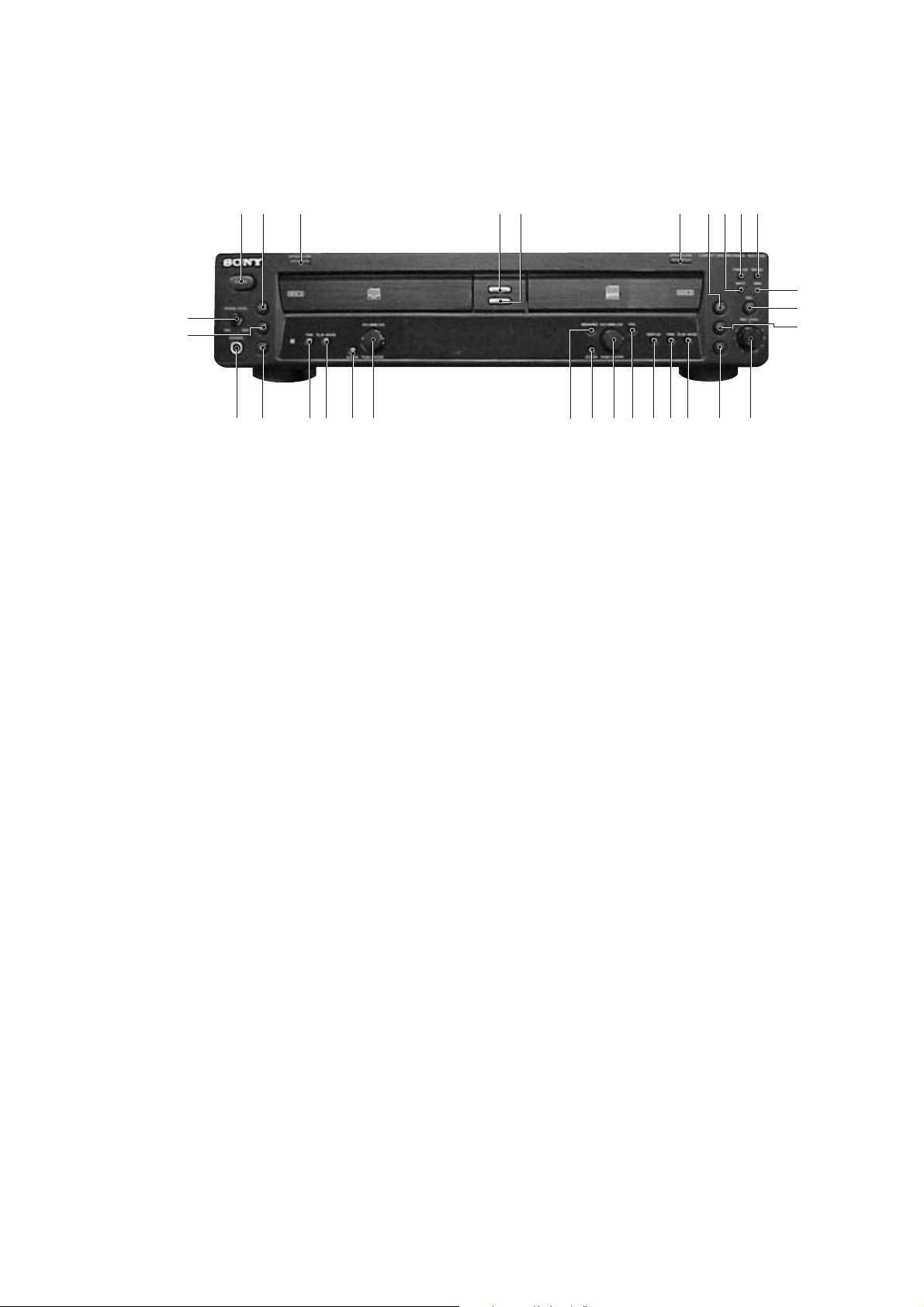
SECTION 2
GENERAL
RCD-W100
3
e;
wl
wgwh ws
1 POWER button
2 H button
3 OPEN/CLOSE button
4 CD SYNCHRO NORMAL button
5 CD SYNCHRO HIGH button
41 2 5 978 q;
qh PLAY MODE button
qj TIME button
qk DISPLAY button
ql YES button
w; l AMS L knob
6
qgqhqjqkqlw;wd wawfwjwk
qf
qa
qs
qd
6 OPEN/CLOSE button
7 H button
8 INPUT button
9 FINALIZE button
q; ERASE button
qa SBM button and indicator
qs REC z button
qd X button
qf REC LEVEL knob
qg x button
wa CLEAR button
ws MENU/NO button
wd l AMS L knob
wf ALBUM button
wg PLAY MODE button
wh TIME button
wj x button
wk PHONES jack
wl X button
e; PHONE LEVEL knob
5
RCD-W100
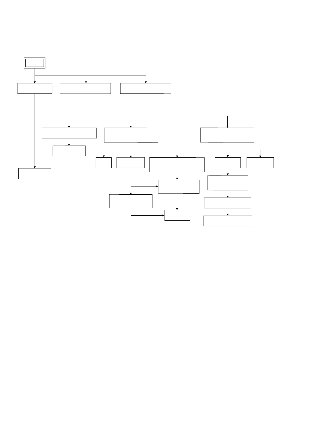
Note : Disassemble the unit in the order as shown below.
SET
SECTION 3
DISASSEMBLY
CASE (409538)
FRONT PANEL SECTION
MAIN BOARD
LOADING PANEL (CD) LOADING PANEL (CDR)
CDR MECHANISM DECK
(CDM65-RBD2)
DISP BOARD
TRAY
MOTOR ASSY
(LOADING) (M201)
CDR BOARD
HOLDER (MG) SUB ASSY,
DUST COVER
OPTICAL PICK-UP
KRM-220CAA
CAM (CH)
CD MECHANISM DECK
(CDM66C-30B61M)
TRAY (66) BD BOARD
OPTICAL BLOCK
SECTION
OP ASSY (A-MAX.4T)
GEAR (LB), GEAR (LA)
6
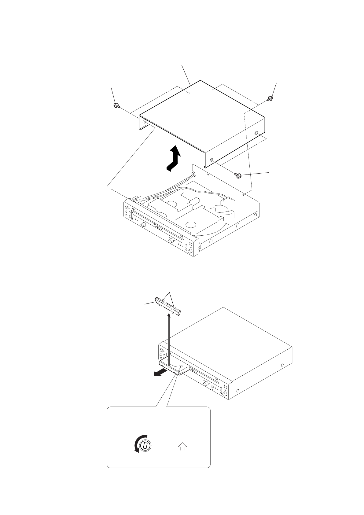
Note : Follow the disassembly procedure in the numerical order given.
)
RCD-W100
3-1. Case (409538)
2
two
screws
(case 3 TP2 3 x 8)
4
case (409538)
3
two
screws
(case 3 TP2 3 x 8
1
two
screws
(case 3 TP2 3 x 8)
3-2. Loading Panel (CD)
5
loading panel (CD)
3
two hooks
4
2
CD mechanism deck (CDM66C-30B61M)
1
Rotate the hole to the direction of arrow.
front panel side
7
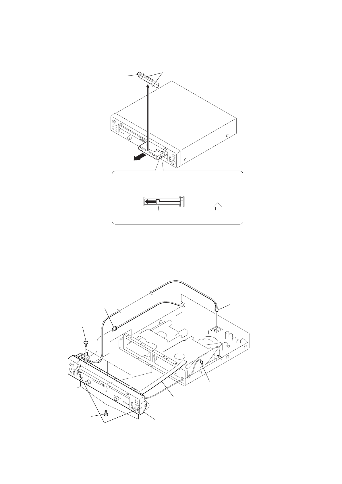
RCD-W100
3-3. Loading Panel (CDR)
5
l
oading panel (CDR)
3
two hooks
4
2
CD mechanism deck (CDM65-RBD2)
1
Slide the lever to the direction of arrow.
3-4. Front Panel Section
4
connector
(2 pin) (CN920)
5
three
screws
(+BVTP 3
×
front panel side
lever
1
c
onnector
(2 pin) (CN900)
8)
2
connector
(3 pin) (CN690)
3
wire (flat type)
(21 core) (CN671)
6
four
screws
×
(+BVTP 3
8)
7
t
wo claws
8
front panel section
8
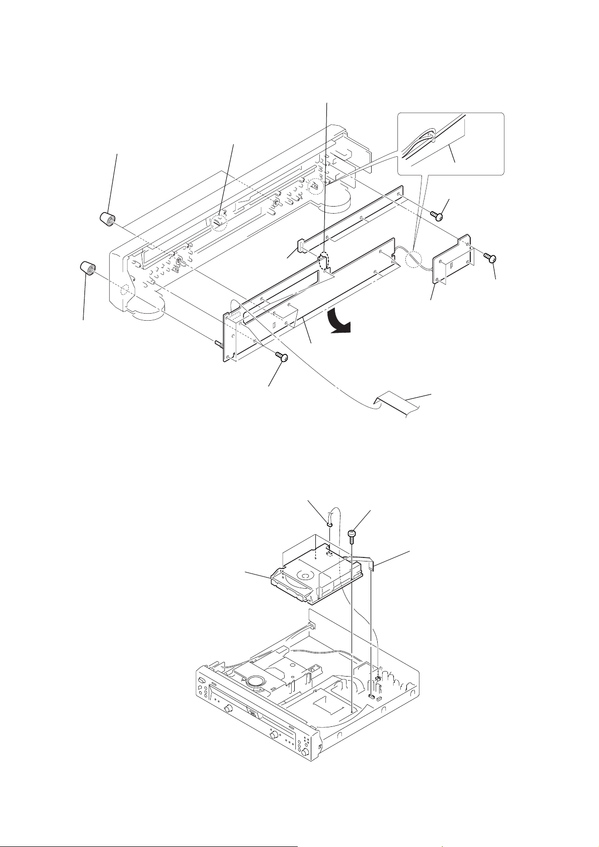
)
)
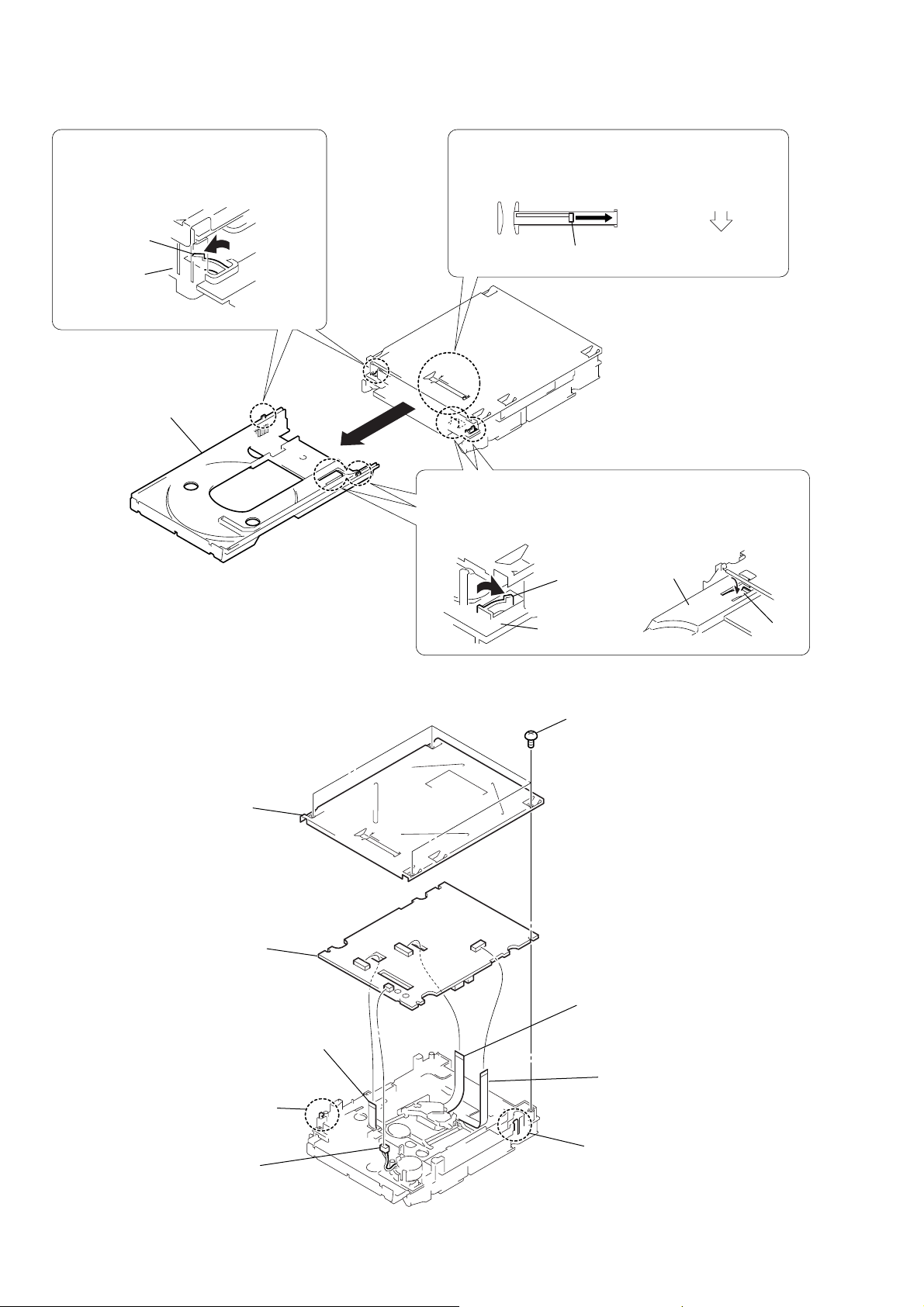
3-5. DISP Board
2
two knobs (AMS)
7
c
law
9
CD-EJECT board
8
Remove the soldering.
HARNESS
PROCESSING
POWER board
5
(+BVTP 2.6
4
SW board
three
RCD-W100
screws
×
8)
3
four
(+BVTP 2.6
screws
×
8
1
knob (AMS)
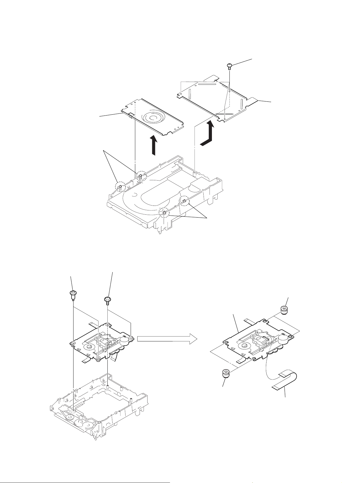
3-6. CDR mechanism deck (CDM65-RBD2)
1
(4 pin) (CN111)
4
CDR mechanism deck
(CDM65-RBD2)
qa
6
twelve
(+BVTP 2.6
screws
connector
DISP board
×
8)
3
four
screws (+BVTP 3
q;
wire (flat type)
(21core) (CN700)
×
8)
2
wire (flat type)
(11core) (CN630
9
RCD-W100
3-7. T ray
2
Pull the tray while pressing the claw of
the chassis in the direction of the arrow.
1
Slide the lever (cam (CH)) to the direction of arrow.
claw
chassis
4
t
3-8. CDR Board
ray
lever (cam (CH))
3
Pull the tray while pressing the claw of the chassis and the claw
of the tray in the direction of the arrow.
claw
chassis
front panel side
tray
claw
2
bottom plate
9
CDR board
5
flexible flat cable
(11 core) (CN103)
6
8
c
onnector
(2 pin) (CN104)
1
four
screws
×
(+BVTP 2.6
3
flexible flat cable
(32 core) (CN101)
4
flexible flat cable
(11 core) (CN102)
c
law
7
c
law
8)
10
r
5
flexible flat cable
(32 core) (from optical device)
1
two step screws
2
two screws
((2X9) (G with), +p tappin)
6
optical pick-up
(KRM-220CAA)
3
two insulators (main)
4
two insulators (main)
3-9. Holder (MG) Sub Assy, Dust Cover
3
holder (MG)
sub assy
1
two claws
4
three s
(+BVTP 2.6
crews
5
dust cove
RCD-W100
×
8)
3-10. Optical Pick-up KRM-220CAA
2
two claws
11
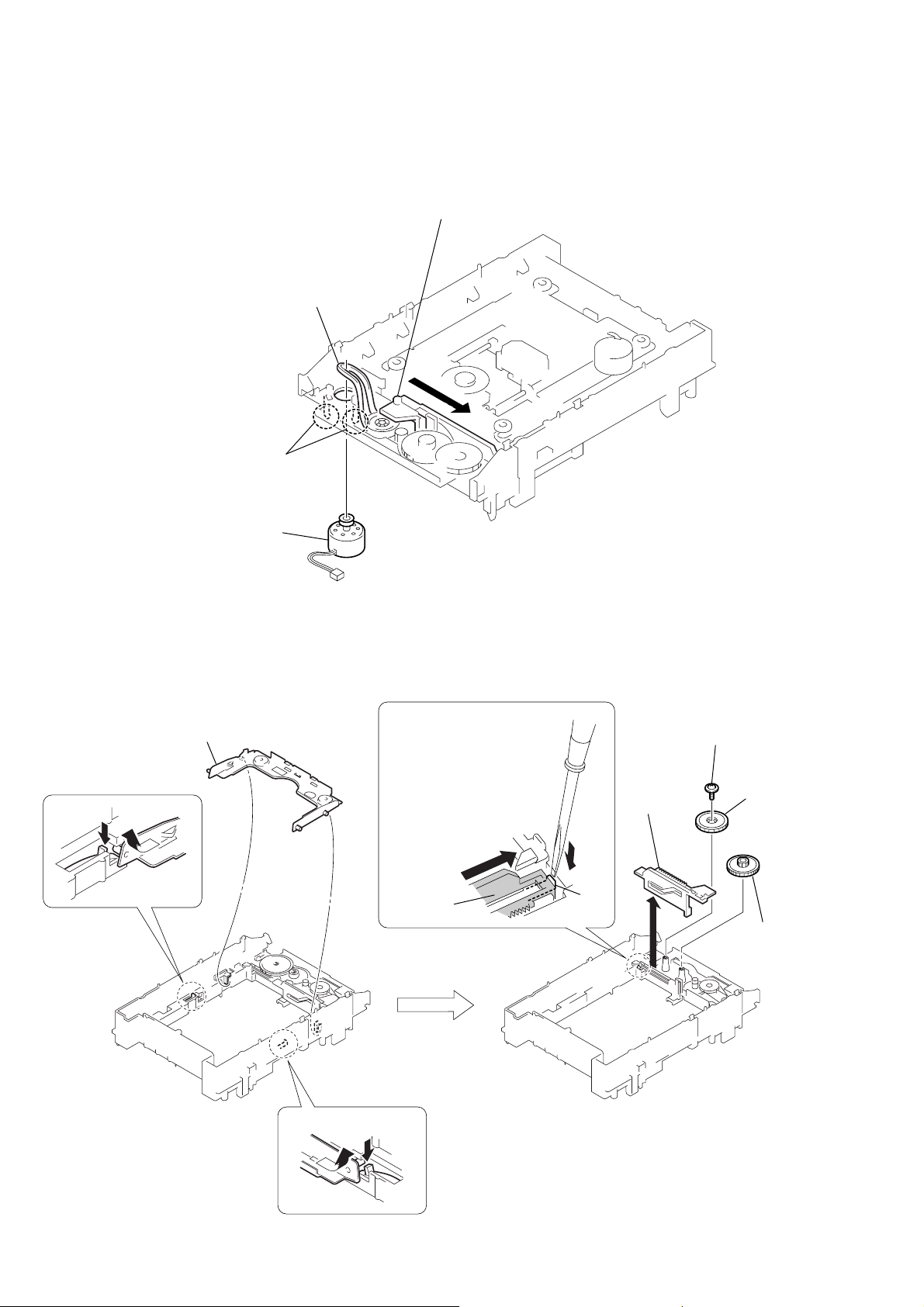
RCD-W100
3-11. Motor Assy (Loading)(M201)
2
Remove the belt (loading) from the
pulley of the motor assy.
3
t
wo claws
1
Slide the cam (CH) to the direction of arrow.
3-12. Cam (CH)
5
holder (BU) sub assy
1
1
4
m
otor assy
(loading) (M201)
1
2
9
Slide the cam (CH) to the
direction of arrow
pressing the claw.
cam (CH)
A
A
while
claw
6
(+PTPWH 2.6
qa
cam (CH)
q;
screw
7
×
8)
g
ear (C)
8
g
ear (B)
12
1
4
1
3
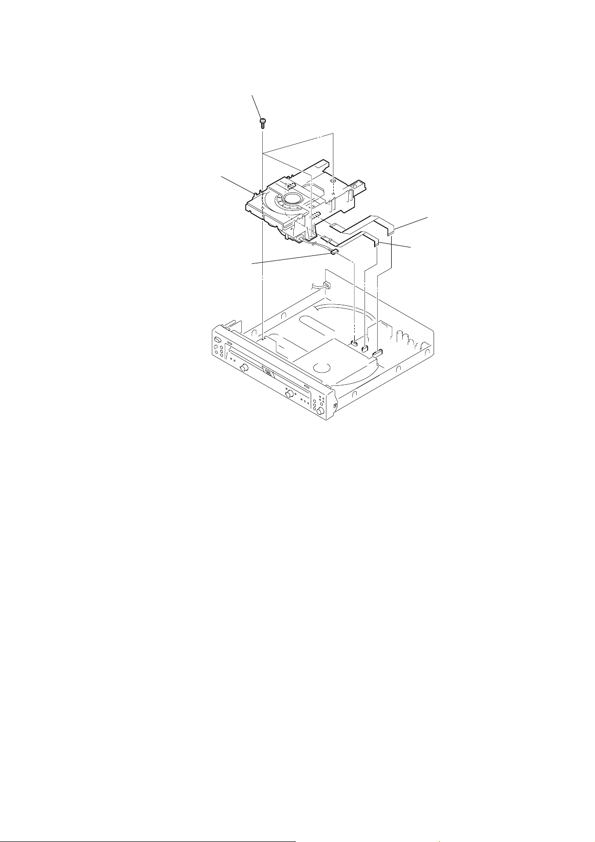
3-13. CD mechanism deck (CDM66C-30B61M)
4
three
screws (+BVTP 3
5
CD mechanism deck
(CDM66C-30B61M)
1
connector
(5 pin) (CN680)
×
RCD-W100
8)
2
wire (flat type)
(25 core) (CN660)
3
wire (flat type)
(9 core) (CN661)
13
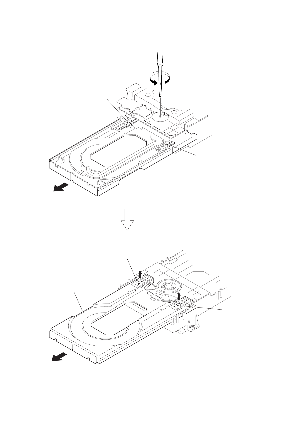
RCD-W100
k
3-14. T ray (66)
3
hook
Turn the cam to the
1
direction of arrow.
4
hook
8
2
tray (66)
6
hook
5
hoo
14
7
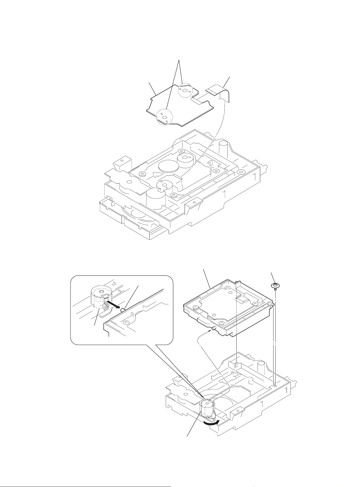
3-15. BD Board
3
BD board
1
Remove soldering from the four points.
2
wire (flat type)
(16 core)
RCD-W100
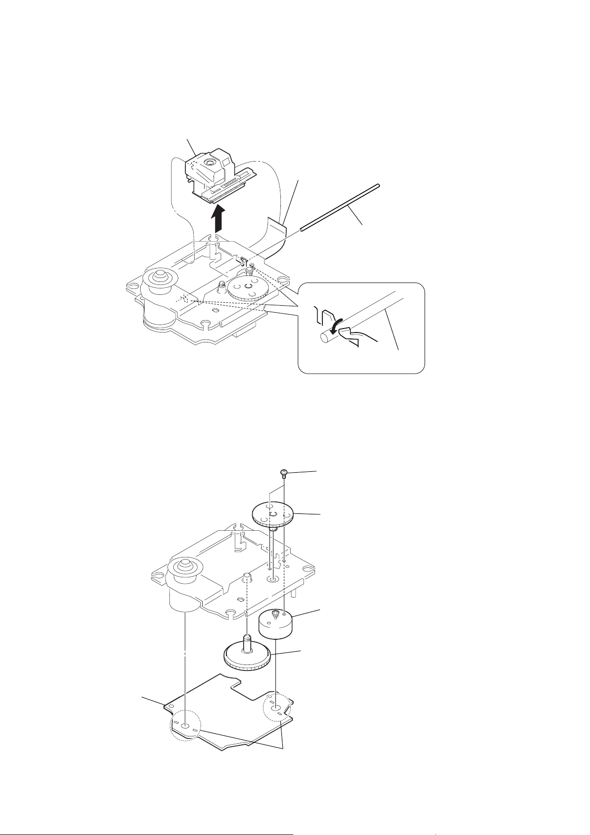
3-16. Optical Block Section
cam (66)
3
shaft (BU holder)
4
optical block section
1
floating screw
2
Rotate the cam (66) in the direction of 2 to move
the shaft (BU holder) upper.
15
RCD-W100
)
3-17. OP Assy (A-MAX.4T)
4
OP assy (A-MAX.4T)
1
flexible flat cable
(16core)
3
sled shaft
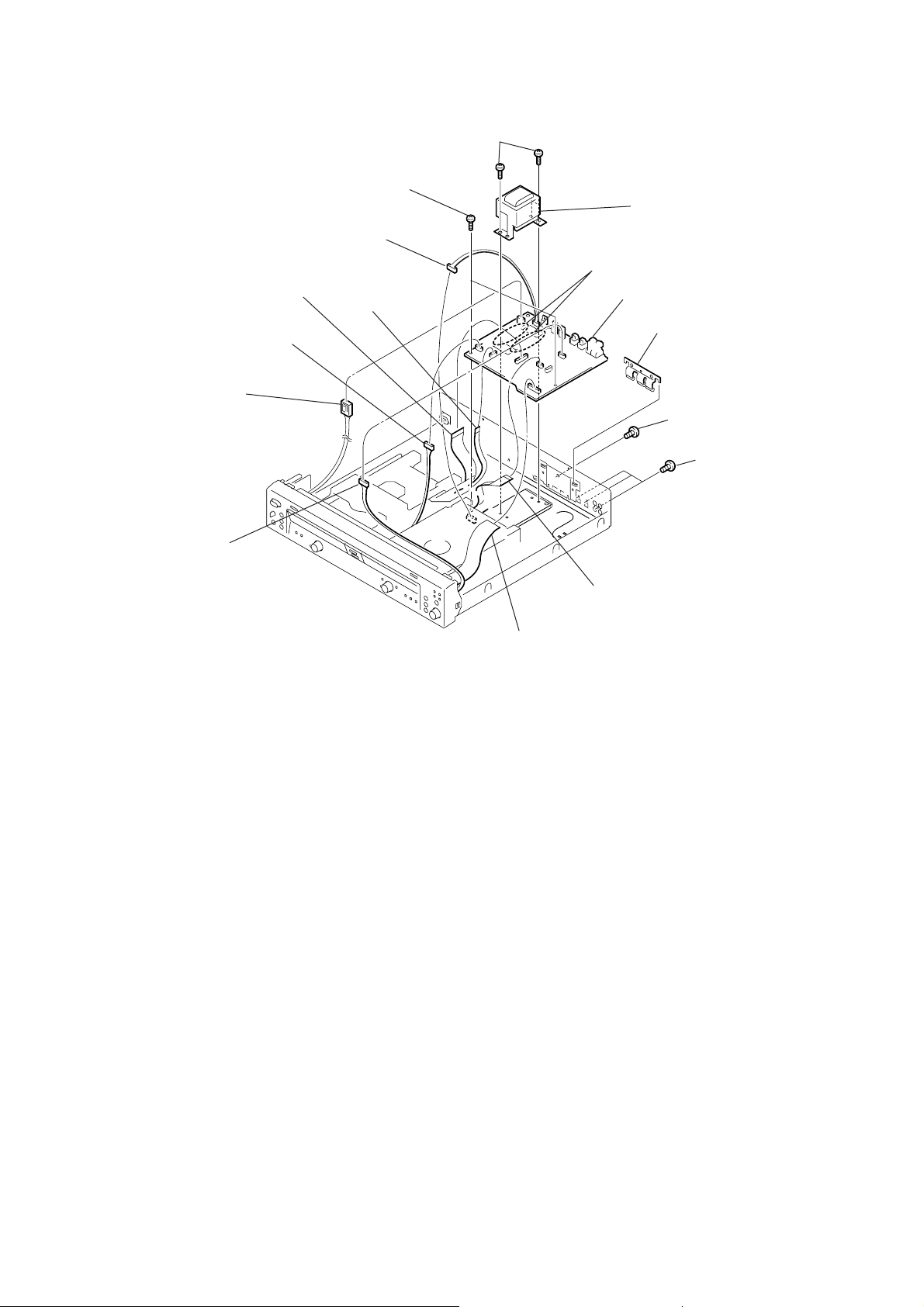
3-18. Gear (LB),Gear (LA)
2
4
two precision
6
gear (LA)
sled shaft
screws (+P 1.7
× 2.2
16
2
BD board
5
sled motor
(M102)
3
gear (LB)
1
Remove soldering from the four points.
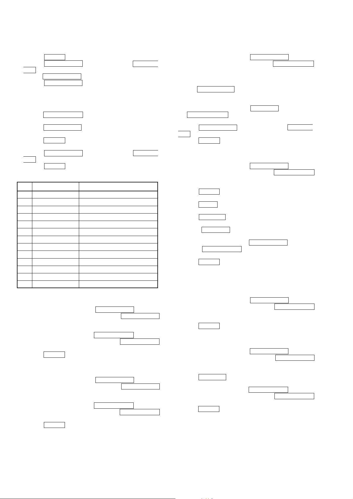
4
connector
(2 pin) (CN900)
2
c
onnector
(3 pin) (CN690)
1
wire (flat type)
(21 core) (CN671)
3
wire (flat type)
(11 core) (CN630)
8
connector
(4 pin) (CN111)
6
wire (flat type)
(25 core) (CN660)
7
wire (flat type)
(9 core) (CN661)
5
connector
(5 pin) (CN680)
qs
two
screws (+BVTT 3
×
6)
qa
three
screws (+BVTP 3
×
8)
9
s
crew (+BVTP 3
×
8)
qd
four
screws (+BVTT 3
×
6)
qf
Remove the soldering.
qh
MAIN board
qg
power transformer
q;
bracket (TR)
3-19. MAIN Board
RCD-W100
17
RCD-W100
SECTION 4
TEST MODE
Setting the Test Mode
Procedure:
1. Press the POWER button to POWER on.
2. Press the l AMS L (DECK A), [SBM] and l AMS
L (DECK B) buttons in order without releasing the button.
3. Turn the l AMS L (DECK B) knob to select the menu.
4. Press the l AMS L (DECK B) knob to execute the test
mode.
Releasing the Test Mode
Procedure 1:
1. Turn the l AMS L (DECK B) knob to select the Ship
Mode.
2. Press the l AMS L (DECK B) knob to execute the Ship
Mode.
3. Press the POWER button to POWER off.
Procedure 2:
1. Press the l AMS L (DECK A), [SBM] and l AMS
L (DECK B) buttons in order without releasing the button.
2. Press the POWER button to POWER off.
Contents of test mode
No. Display Function
1 SYS Version System version display
2 CDR Version CDR version display
3BU Test Deck A BU test mode
4 SERVICE Deck A Service mode
5 Ship Mode CD Shipment mode
6 FL ALL ON Fluorescent indicator tube test
7 FL ALL OFF Fluorescent indicator tube test
8 FL ITIMATSU Fluorescent indicator tube test
9 LED CHECK LED check
10 KEY CHECK Keyboard check
11 RM CHECK Remote commander check
12 CDR History CDR error history display
13 Play Speed Deck A x4 speed
System Version Display
Procedure:
1. Enter the test mode, then turn the l AMS L (DECK B)
knob to display “SYS Version”, and press the l AMS L
(DECK B) knob.
2. The system version is displayed.
3. To exit from this mode, turn the l AMS L (DECK B)
knob to display “Ship Mode”, and press the l AMS L
(DECK B) knob to execute the Ship Mode.
4. Press the POWER button to POWER off.
CDR Version Display
Procedure:
1. Enter the test mode, then turn the l AMS L (DECK B)
knob to display “CDR Version”, and press the l AMS L
(DECK B) knob.
2. The CDR version is displayed.
3. To exit from this mode, turn the l AMS L (DECK B)
knob to display “Ship Mode”, and press the l AMS L
(DECK B) knob to execute the Ship Mode.
4. Press the POWER button to POWER off.
BU Test Mode (Deck A)
Procedure:
1. Enter the test mode, then turn the l AMS L (DECK B)
knob to display “BU Test”, and press the l AMS L
(DECK B) knob.
2. “bdt S CURVE” is displayed. This test mode is used in the Electrical Adjustment section.
3. Turn the l AMS L (DECK B) knob . “bdt RAM READ”,
“bdt RAM WRITE”, “bdt COMOUT”, “bdt FB TUNE” and “bdt
ERR RATE” are displayed.
4. To exit from this mode, press the MENU/NO button and turn
the l AMS L (DECK B) knob to display “bdt ERR
RATE”.
5. Press the l AMS L (DECK A), [SBM] and l AMS
L (DECK B) buttons in order without releasing the button.
6. Press the POWER button to POWER off.
Service Mode (Deck A)
Procedure:
1. Enter the test mode, then turn the l AMS L (DECK B)
knob to display “SERVICE”, and press the l AMS L
(DECK B) knob.
2. “SERVICE MODE” is displayed.
3. Press the ERASE button, “SLED OUT” is displayed and the
sled moves to the outermost direction.
When the ERASE button is released, “SLED STOP” is displayed
and the sled stops.
4. Press the FINALIZE button, “SLED IN” is displayed and the
sled moves to the innermost direction.
When the FINALIZE button is released, “SLED STOP” is
displayed and the sled stops.
5. To exit from this mode, press the l AMS L (DECK A),
[SBM] and l AMS L (DECK B) buttons in order with-
out releasing the button.
6. Press the POWER button to POWER off.
Note: Always move the pick-up to the most inside position when
exiting from this mode.
Ship Mode
Procedure:
1. Enter the test mode, then turn the l AMS L (DECK B)
knob to display “Ship Mode”, and press the l AMS L
(DECK B) knob.
2. “Push POWER!” is displayed.
3. Press the POWER button to POWER off.
FL ALL ON Mode
Procedure:
1. Enter the test mode, then turn the l AMS L (DECK B)
knob to display “FL ALL ON”, and press the l AMS L
(DECK B) knob.
2. All segments of fluorescent indicator tube and LED turn on.
3. Press the MENU/NO button, then “FL ALL ON” is displayed
again.
4. To exit from this mode, turn the l AMS L (DECK B)
knob to display “Ship Mode”, and press the l AMS L
(DECK B) knob to execute the Ship Mode.
5. Press the POWER button to POWER off.
18
RCD-W100
FL ALL OFF Mode
Procedure:
1. Enter the test mode, then turn the l AMS L (DECK B)
knob to display “FL ALL OFF”, and press the l AMS L
(DECK B) knob.
2. All segments of fluorescent indicator tube and LED turn off.
3. Press the MENU/NO button, then “FL ALL OFF” is displayed
again.
4. To exit from this mode, turn the l AMS L (DECK B)
knob to display “Ship Mode”, and press the l AMS L
(DECK B) knob to execute the Ship Mode.
5. Press the POWER button to POWER off.
FL ITIMATSU Mode
Procedure:
1. Enter the test mode, then turn the l AMS L (DECK B)
knob to display “FL ITIMATSU”, and press the l AMS
L (DECK B) knob.
2. Checkered patterns of segments are displayed.
3. Press the MENU/NO button, then “FL ITIMA TSU” is displayed
again.
4. To exit from this mode, turn the l AMS L (DECK B)
knob to display “Ship Mode”, and press the l AMS L
(DECK B) knob to execute the Ship Mode.
5. Press the POWER button to POWER off.
LED Check Mode
Procedure:
1. Enter the test mode, then turn the l AMS L (DECK B)
knob to display “LED CHECK”, and press the l AMS L
(DECK B) knob.
2. Turn the l AMS L (DECK A) or (DECK B) knob clock-
wise.
3. Press the MENU/NO button, then “LED CHECK” is displayed
again.
4. To exit from this mode, turn the l AMS L (DECK B)
knob to display “Ship Mode”, and press the l AMS L
(DECK B) knob to execute the Ship Mode.
5. Press the POWER button to POWER off.
CDR History Display
Procedure:
1. Enter the test mode, then turn the l AMS L (DECK B)
knob to display “CDR History”, and press the l AMS L
(DECK B) knob.
2. “00 ######## ########” is displayed as the first error hitory.
3. Turn the l AMS L (DECK B) knob to select the error
history. The number of error histories is ten in all.
(Refer to “Contents of CDR error history”.)
4. Press the MENU/NO button, then “CDR History” is displayed
again.
5. To exit from this mode, turn the l AMS L (DECK B)
knob to display “Ship Mode”, and press the l AMS L
(DECK B) knob to execute the Ship Mode.
6. Press the POWER button to POWER off.
Play Speed Selection Mode (Deck A)
Procedure:
1. Enter the test mode, then turn the l AMS L (DECK B)
knob to display “Play Speed”, and press the l AMS L
(DECK B) knob.
2. “x4 Play” is displayed. If a CD is in the deck A, pressing the
H button executes the 4 times speed playback.
3. Press the x button to stop the playback.
4. Press the MENU/NO button, then “Play Speed” is displayed
again.
5. To exit from this mode, turn the l AMS L (DECK B)
knob to display “Ship Mode”, and press the l AMS L
(DECK B) knob to execute the Ship Mode.
6. Press the POWER button to POWER off.
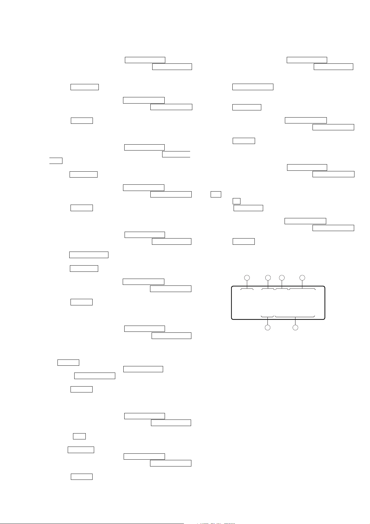
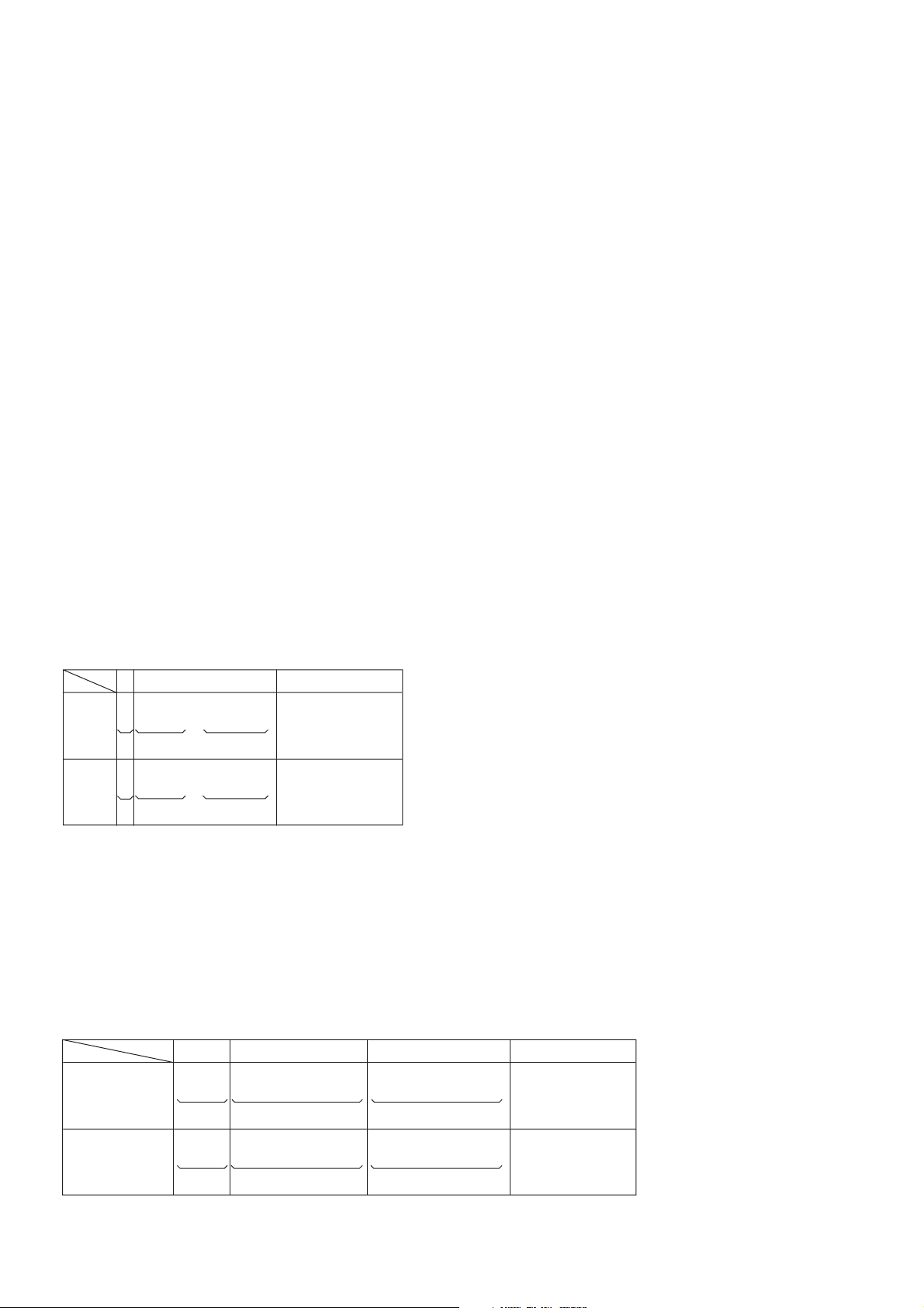
Contents of CDR error history
display(example)
1 2
3 4
00 05070D80
KEY Check Mode
Procedure:
1. Enter the test mode, then turn the l AMS L (DECK B)
knob to display “KEY CHECK”, and press the l AMS L
(DECK B) knob.
2. “Got 0 keys” is displayed.
3. Press the buttons, and when all the buttons are pressed (without
the POWER button), “Got 26 keys” will be displayed.
4. T o exit fr om this mode, press the l AMS L (DECK A),
[SBM] and l AMS L (DECK B) buttons in order with-
out releasing the button.
5. Press the POWER button to POWER off.
Remote Commander Check
Procedure:
1. Enter the test mode, then turn the l AMS L (DECK B)
knob to display “RM CHECK”, and press the l AMS L
(DECK B) knob.
2. Press the H key on the remote commander, then “Got
PlayCom” is displayed.
Press the MENU/NO button, then “RM CHECK” is displayed again.
3.
4. To exit from this mode, turn the l AMS L (DECK B)
knob to display “Ship Mode”, and press the l AMS L
(DECK B) knob to execute the Ship Mode.
5. Press the POWER button to POWER off.
000E2E0D
5 6
(hexadecimal)
1 Order of the error history
00 to 09: ten error histories in all
2 Error contents
01: unable to focus on
02: Q code/ATIP discontinuous (several frames preceding)
03: Q code/ATIP unreadable
04: search taking more than sixteen seconds
05: focus failure
06: sled over run
07: not passing by start time to write
08: audio buffer over
09: sync failure
OA: Spindle lock taking more than 8 secouds
example : 05 is focus failure
19
RCD-W100
3 Operation mode
bit 7: Speed
0: normal speed
1: x4 speed
bit 6 to bit 0: Number of inner condition
01: POWER off condition/during shift to POWER on
02: POWER off and shipment setting/during shift to PO WER
off and shipment setting
03: stop condition/during stop
04: during start up of servo
05: during TOC reading and others
06: during CD TEXT reading
07: during standby(waiting for command from the CD sys-
tem)/during search
08: during playback
09: during manual search(playback)
0A:during pause
0B:during manual search(pause)
0C:during OPC
0D:recording standby/during recording pause
(enable to shift to recording)
0E: during recording
0F: unable to record (waiting for shift to being recordable)
10: PMA updating
11: during operation of unfinalize
12: during operation of finalize
13: PMA erasing
14: emergency
15: recording preparation
16: recording end
5 Write POWER (integer of mW x 10, av ailab le during write
processing)
examples: 00 means unavailable
(when 3 operation mode is not recording)
: A3 means 163(decimal), i.e. 16.3 mW
6 ATIME (min)/(sec)/(frame)
example: 0E, 2E, 0D means 14 : 46 : 13
Abbreviations:
ATIP : Absolute Time In Pre-groove
OPC : Optimum Power Control
PMA : Program Memory Area
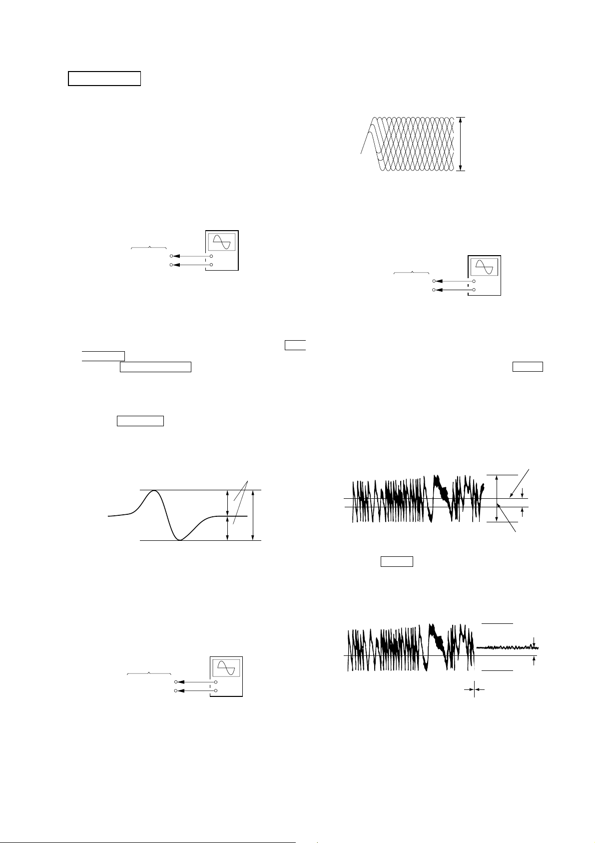
examples :
bit
HEX
77654 321
0000 0111
07
00
1001 0001
91
11 1
4 Start time of read in(compression method)
bit 15 to bit 13 : (min)
0: 97 min
1: 96 min
2: 95 min
7: others
bit 12 to bit 7: (sec)
bit 6 to bit 0: (frame)
examples :
HEX
bit
0 Operation mode
normal speed, during
standby(waiting for
command from the CD
system)/during search
during operation of
0000 1101 1000 0000
0D,80
97(min) 27(sec)
x4 speed,
unfinalize
7
654 321
0(frame)
015 14 13 12 11 10 9 8 Start time of read in
97 : 27 : 00
11,16
20
0001 0001 0001 0110
34(sec)97(min) 22(frame)
97 : 34 : 22
SECTION 5
e
y
e
ELECTRICAL ADJUSTMENTS
RCD-W100
CD SECTION (DECK A)
Note :
1. CD Block is basically designed to operate without adjustment.
Therefore, check each item in order given.
2. Use YEDS-18 disc (3-702-101-01) unless otherwise indicated.
3. Use an oscilloscope with more than 10MΩ impedance.
4. Clean the object lens by an applicator with neutral detergent
when the signal level is low than specified value with the
following checks.
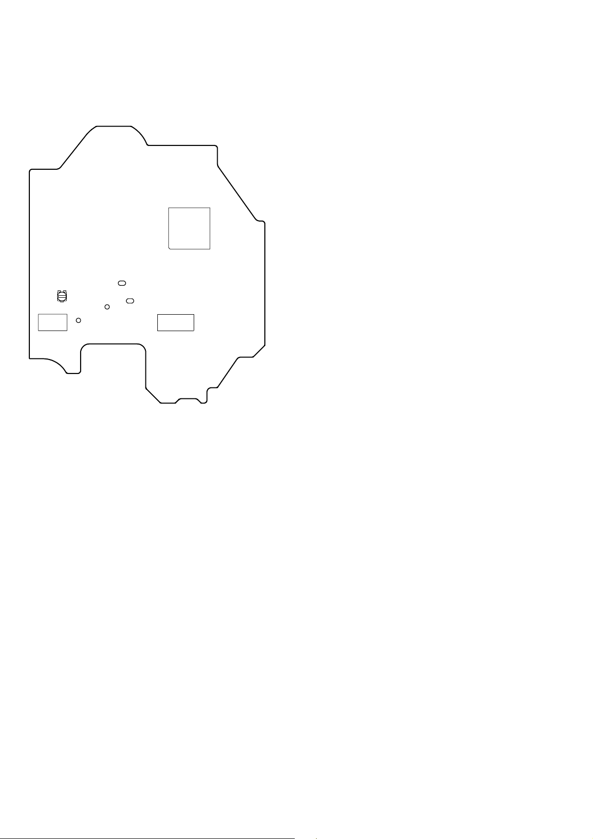
S Curve Check
Connection :
oscilloscop
(DC range)
BD board
TP4 (FE)
TP7 (VC)
Procedure :
1. Connect an oscilloscope to test point TP4 (FE) and TP7 (VC)
on the BD board.
2. Turn the power on.
3. Load the disc (YEDS-18).
4. Enter the test mode, select the BU Test and press the l
AMS L (DECK B) knob to display “bdt S CURVE”.
5. Press the l AMS L (DECK B) knob. “LD AL” is
displayed and playback starts automatically.
6. Check the oscilloscope waveform (S-curve) is symmetrical
between A and B. And confirm peak to peak level within 3.6 ±
0.5 Vp-p.
7. Press the MENU/NO button to stop playback.
8. Exit from the test mode.
(Refer to the TEST MODE Section)
+
–
symmetr
A
Note: A clear RF signal waveform means that the shape “◊” can be
clearly distinguished at the center of the waveform.
VOLT/DIV : 200mV
TIME/DIV : 500ns
level : 1.1 ± 0.3Vp-p
Checking Location : BD board (Side B)(See page 22)
E-F Balance Adjustment
Connection :
oscilloscope
(DC range)
BD board
TP2 (TE)
TP7 (VC)
+
–
Procedure:
1. Connect an oscilloscope to TP2 (TE) and TP7 (VC) on the BD
board.
2. Turn the power on.
3. Load the disc (YEDS-18) and playback the number f i ve trac k.
4. Enter the Service Mode. (see page 18) Press the INPUT button
until “TRV ON” is displayed. (The tracking servo and the
sledding servo are turned off.)
5. Check the level B of the oscilloscope waveform. Rotate the
RV101 on the BD board and adjust so that the A (DC voltage)
of the center of the traverse waveform becomes 0 volt.
Traverse Wa v ef orm
0V
Center of
the waveform
B
A (DC
voltage)
B
Note: Try to measure several times to make sure than the ratio of A
: B or B : A is more than 10 : 7.
Checking Location : BD board (Side B)(See page 22)
RF Level Check
Connection :
oscilloscop
(AC range)
BD board
TP8 (RFAC)
TP7 (VC)
+
–
Procedure :
1. Connect an oscilloscope to TP8 (RFAC) and TP7 (VC).
2. Turn the power on.
3. Load the disc (YEDS-18) and playback the number five track.
4. Confirm that oscilloscope waveform is clear and check RF signal
level is correct or not.
level: 1.1 ± 0.5 Vp-p
6. Press the INPUT button until “TRV OFF” is displayed and
the tracking servo and the sledding servo are turned on. Confirm
that the C (DC voltage) is almost equal to the A (DC voltage).
Traverse Wa v ef orm
0V
Tracking servo
Sled servo
OFF
Tracking servo
Sled servo
ON
C (DC
voltage)
7. Exit from the test mode. (see page 18)
Checking Location : BD board (Side B)(See page 22)
Adjustment at Replacement of CD Base Unit
(BU-30BBD61M)
Perform the E-F Balance Adjustment at replacement of CD base
unit (BU-30BBD61M).
21
RCD-W100
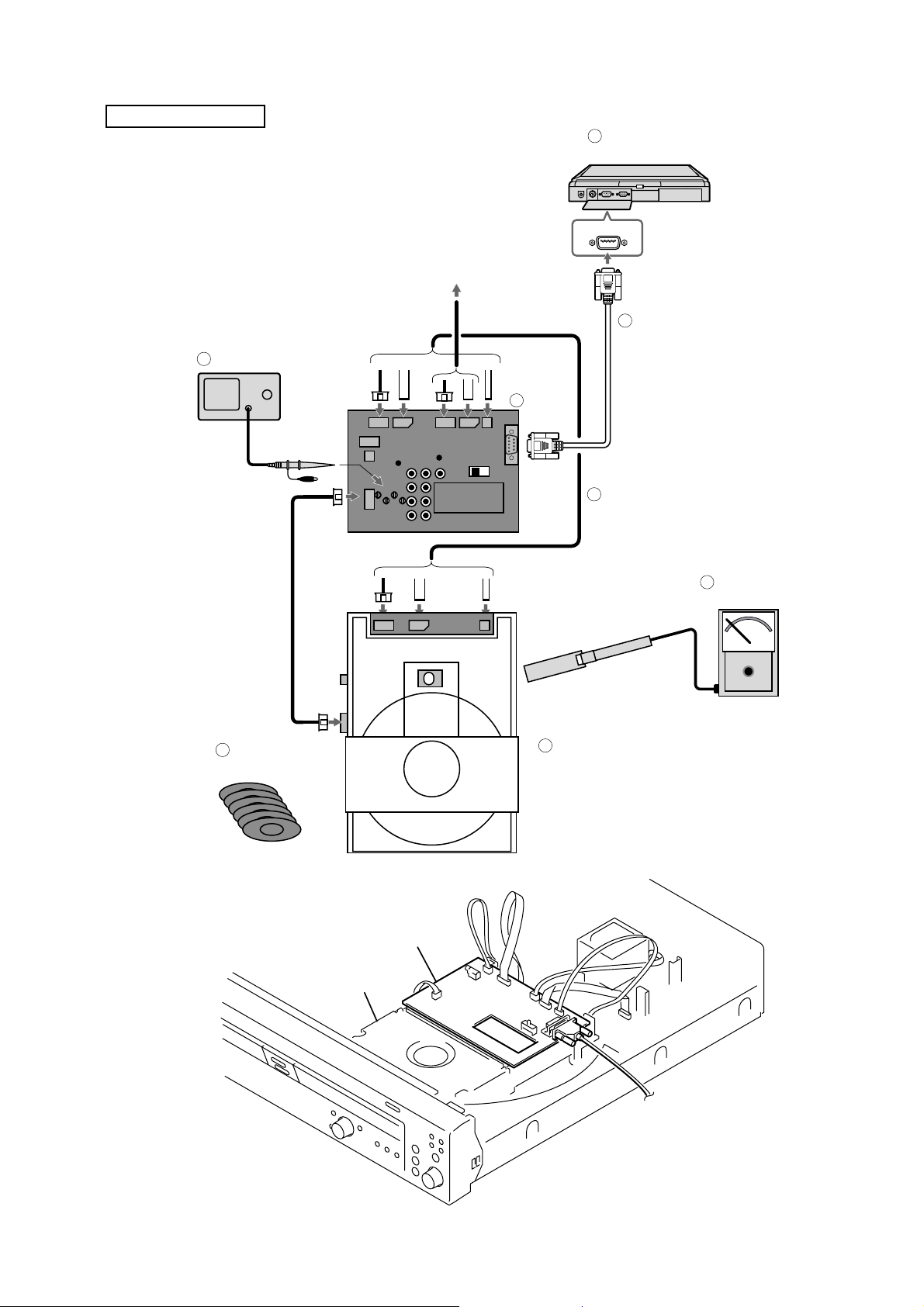
Adjustment and Checking Location:
[BD BOARD] — SIDE B —
IC101
RV101
E-F Balance
Adjustment
TP7
(VC)
IC103
TP8
(RFAC)
TP2
(TE)
TP4
(FE)
IC102
22
CD-R/RW SECTION
*The following is the method of locating the faulty point and
electrical adjustment.
1. Connection and Setting of Programs
PC
3
(w/SerialI/F)
RCD-W100
1-1. Connection
5
Oscilloscope
(A)
MPXOUT
To
RCD-W100
(B) (C) (D)
0-756-358-11
CDM65-RBD1 SERVICE
RESET
Jig
CONTROL FIRM
(B) (C) (D)
COM1
8
RS-232C
Jig
2
9
Cables for Jig connecting
Cable
6
Laser Power
Meter
7
Test Disc
CDM65-RBD2
jig
1
CDM65-RBD2
v Fig. Position of Jig (Set the jig after removing the cover of CDM65-RBD2)
23
RCD-W100
1-2. Equipments to prepare
1 Test Object Both RBD2 and CDM65-RBD2 shall be tested.
RBD2 : Flash Memory Writing of of
Circuit Test by Self-diagnostics
CDM65-RBD2 : Electrical Adjustment
Performance Test
2 Jig (With 9 Cables, Parts No.J-2501-233-A)
3 PC Windows95/98/2000/Me with COMport (RS-232C)
4 Programs TeraTerm Pro + Service macro
5 Oscilloscope More than 150MHz
6 Laser Power Meter LEADER LPM-8001 (Parts No.J-2501-046-A)
7 Test Disc
PATD-012 : (Parts No.4-225-203-1) Adjustment for Playback (CD,CD-R)
TCD-W091W : (Parts No.J-2501-226-A) Adjustment for Playback (CD-RW)
CRM74 (Blank CD-R) : Adjustment and Check for Recording (CD-R)
CWM74 (Blank CD-RW) : Check for Recording (CD-RW)
TCD-W032W : (Parts No.J-2501-227-A) Defocus tolerance (CD-RW)
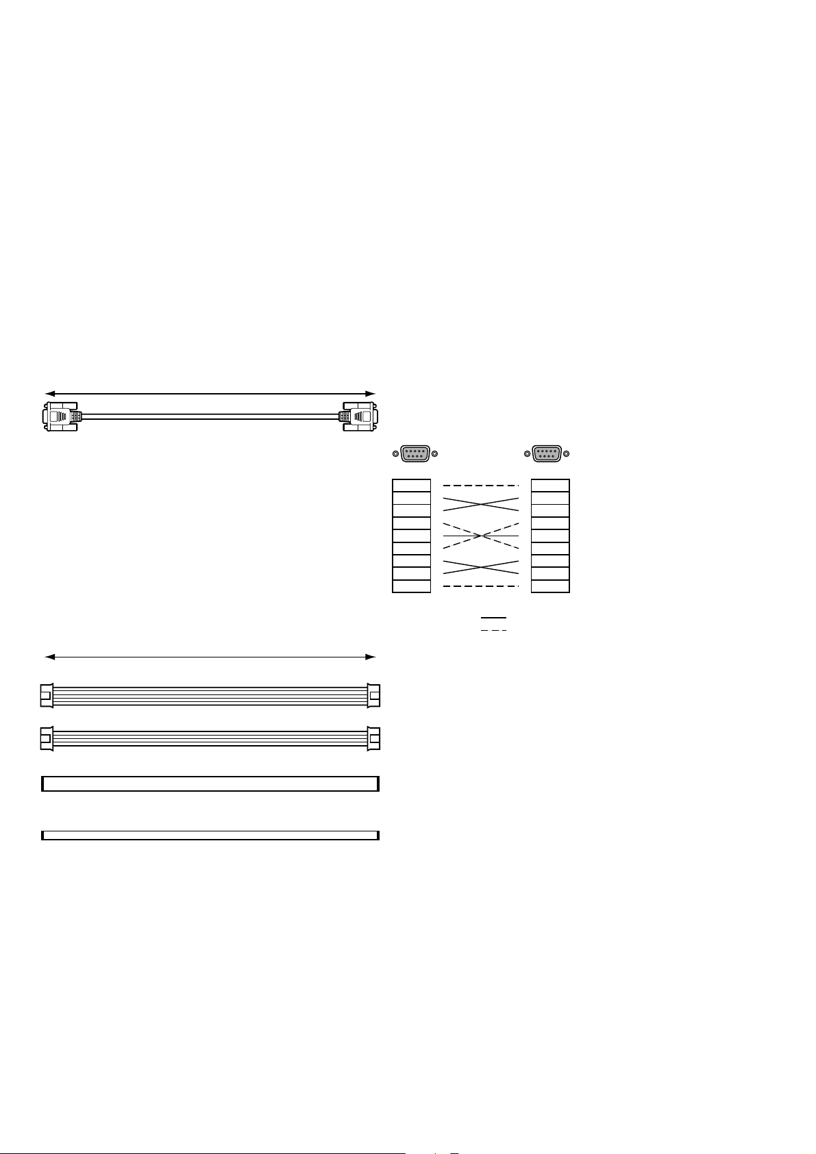
8 RS-232C Cable
L=2000mm
(E)
D-sub 9pin Female cross cable
54321
9876
1
2
3
4
5
6
7
8
9
54321
9876
1
2
3
4
5
6
7
8
9
9 Cables for Jig connecting
:mandatory
: not use
L=300mm
(A)
PH 5p
(B)
PH 4p
(C)
FFC 11p 1.0mm pitch (J-2501-200-A)
(D)
FFC 5p 1.0mm pitch (J-2501-212-A)
24
1-3. Setting of Programs (Tera Term Pro and Service macro)
* Confirmation of System (Windows 98 is used in this explanation) Preparation for Terminal software
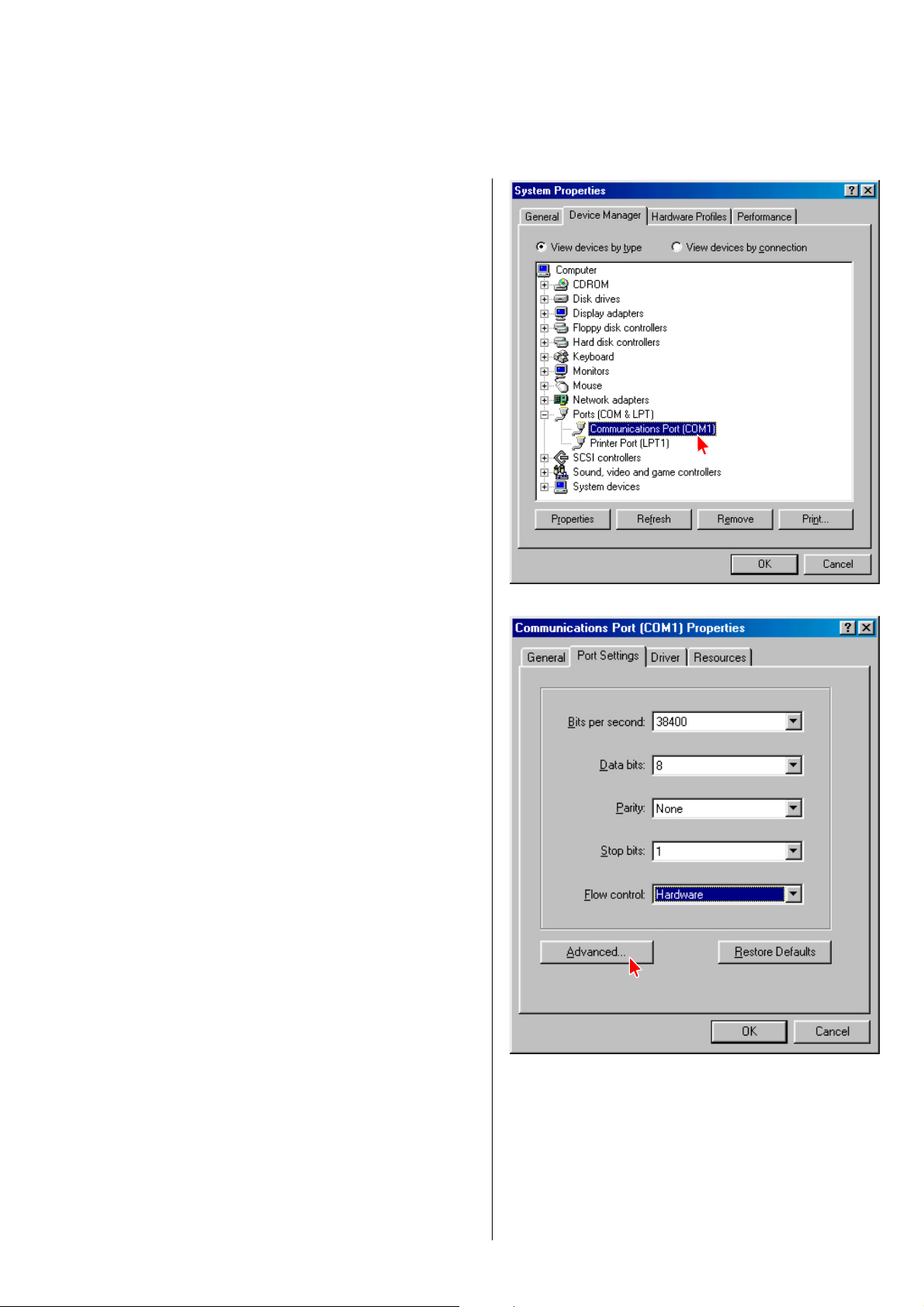
1) Set up the serial port from OS.
a) Select Start → Settings → Control Panel and select System →
Device manager → Communication Port (COMn)
(see Fig. 1-1)
* Specify the COM port that connected with JIG of CDM65.
RCD-W100
b) Double click COMn (as you connect to the Jig-CDM65)
Set the parameters as below.
Bits per second : 38400
Data bits : 8
Parity : non
Stop bits : 1
Flow control : hardware
(see Fig.1-2)
4 Fig. 1-1
4 Fig. 1-2
25
RCD-W100
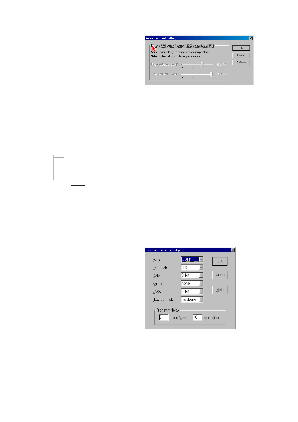
c) Press “Advanced...” button (see Fig.1-2)
Remove the check “Use FIFO buffers ...”
(see Fig.1-3)
4 Fig. 1-3
2) Unzip the file “ttermp231.zip” by PC.
(The file “ttermp231.zip” is distributed together with the service manual.)
3) After unzip the files, you can find setup.exe .
Double click the setup.exe.
Please install as the installer is.
Do not change the directory that files are installed. (use default)
4) Unzip the file “030416_Service.zip” by PC.
Copy all “ttl” file and “FUNC” folder which are contained in “030416_Service” and paste them in the “Ttermpro” file as below.
(The file “030416_Service.zip” is distributed together with the service manual.)
Ttermpro
01ldp_S.ttl
...
10vwdcC_S.ttl
FUNC
AMS.ttl
...
VERCHK.ttl
4 Fig. 1-4
Note : Do not change the directory path.
5) Start-up the TeraTermPro
Double click the ttermpro.exe.
6) Set up the TeraTermPro (IMPORTANT!!)
a) Select Setup → Serial Port... and set the parameters as below.
Port : (As you connect to the Jig-CDM65)
Baud rate : 38400
Data : 8 bit
Parity : none
Stop : 1 bit
Flow control : hardware
Transmit delay : 0 msec/char 10 msec/line
After settings, press “OK” button. (see Fig.1-5)
26
4 Fig. 1-5
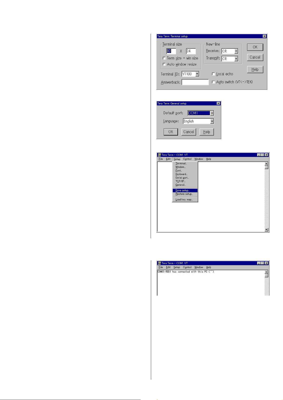
b) Terminal setup
Set the parameters as below.
New-line receive : CR
transmit : CR
After settings, press “OK” button. (see Fig.1-6)
c) General setup
Select the language and press “OK” button. (see Fig.1-7)
RCD-W100
4 Fig. 1-6
4 Fig. 1-7
d) Saving the setup
Select Setup → Save setup... and save as teraterm.ini in the
Ttermpro directory. (see Fig.1-8)
7) Connect the JIG and CDM65.
8) Confirm the S510 on JIG is ‘CONTROL’.
9) Power on the CDM65 and press SW101(RESET) on JIG.
“CDM65-RBD1 has connected with this PC (^^)” is displayed.
(see Fig.1-9)
If above message is not displayed, you may hav e some mistakes.
Please confirm previous setting procedures again.
4 Fig. 1-8
4 Fig. 1-9
27
RCD-W100
2.
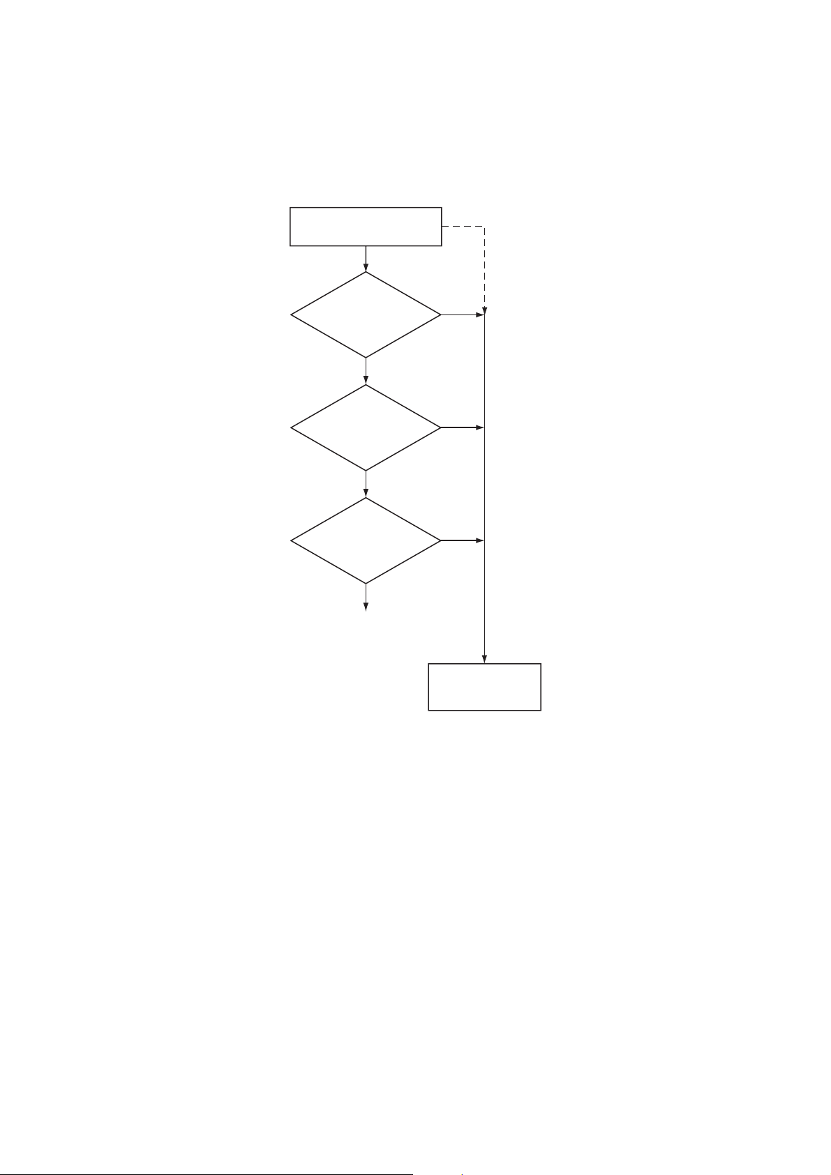
Repair Works That Require Electrical Adjustment
In the case of repair works as shown below, electrical adjustment is required.
Locating the faulty point
KRM-220CAA
is replaced.
No
RBD2
is replaced.
No
The parts shown
in the List (1)
is replaced.
No
Electrical adjustment
is not required.
Yes
Yes
Yes
Electrical adjustment
28
List (1) : IC101, IC103, IC171, IC201, IC502
3. Locating the Faulty Point
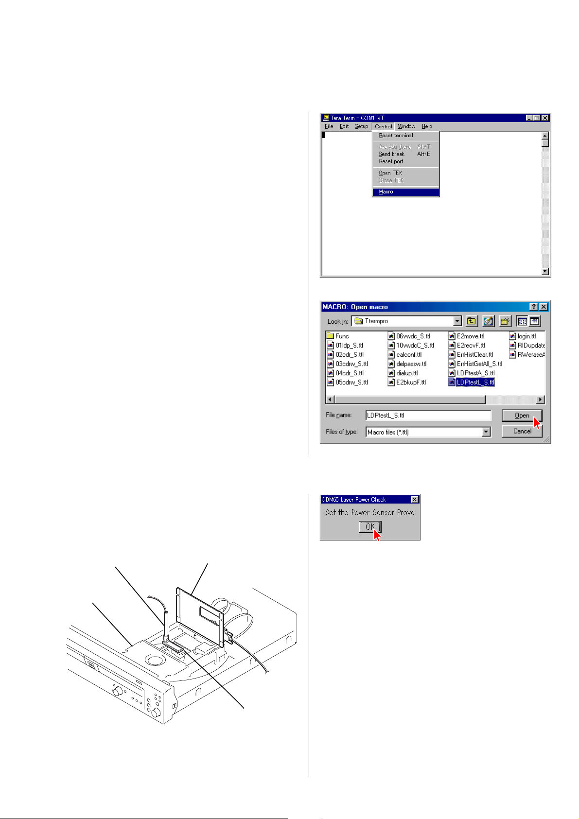
3-1. Laser Power Check
1) Select the menu as follows. Control → Macro, and select
LDPtestL_S.ttl.
Press “Open”. (Fig. 3-1, 3-2)
RCD-W100
4 Fig. 3-1
4 Fig. 3-2
2) Press the “RESET” button (SW101) of the jig as prompted by the display.
3) Place probe of a laser power meter in the specified position
following the display as shown in Fig. 3-3. (See Fig. 3-3-a)
4 Fig. 3-3
sensor probe
CDM65-RBD2
jig
optical pick-up
4 Fig. 3-3-a
Note : Do not add stress to an optical pick-up.
29
RCD-W100
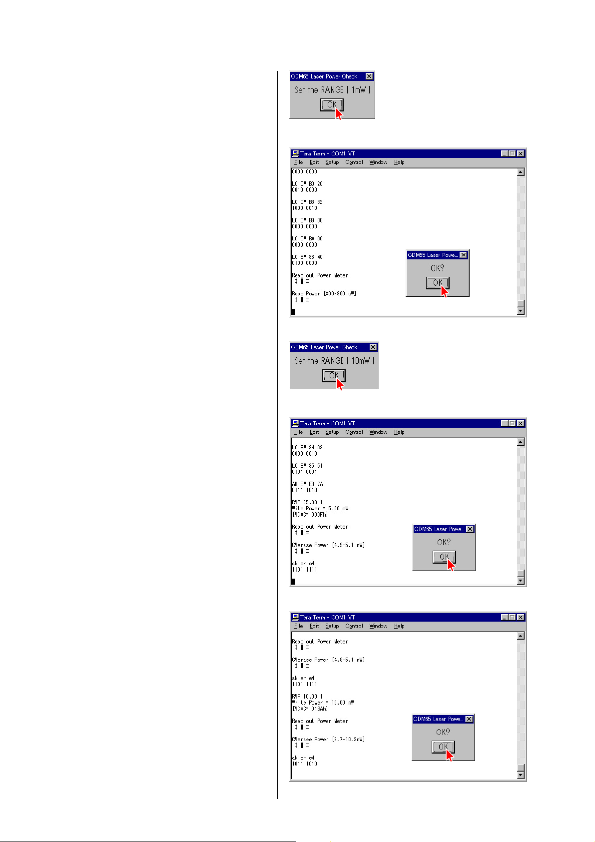
4) When the display shown in Fig. 3-4 appears, set the Range of a
laser power meter to “1 mW” and press “OK”.
5) Check that the laser power meter reading satisfies the following
requirement. When the laser power satisfies the required
specification, press “OK”. (Fig. 3-5)
LEADER LPM-8001 : 0.76 to 0.86 mW
4 Fig. 3-4
6) When the display shown in Fig. 3-6 appears, set the Range of a
laser power meter to “10 mW” and press “OK”.
7) Check that the laser power meter reading satisfies the following
requirement. When the laser power satisfies the required
specification, press “OK”. (Fig. 3-7)
LEADER LPM-8001 : 4.5 to 4.7 mW
4 Fig. 3-5
4 Fig. 3-6
4 Fig. 3-7
8) Check that the laser power meter reading satisfies the following
requirement. When the laser power satisfies the required
specification, press “OK”. (Fig. 3-8)
LEADER LPM-8001 : 9.2 to 9.6 mW
30
4 Fig. 3-8
 Loading...