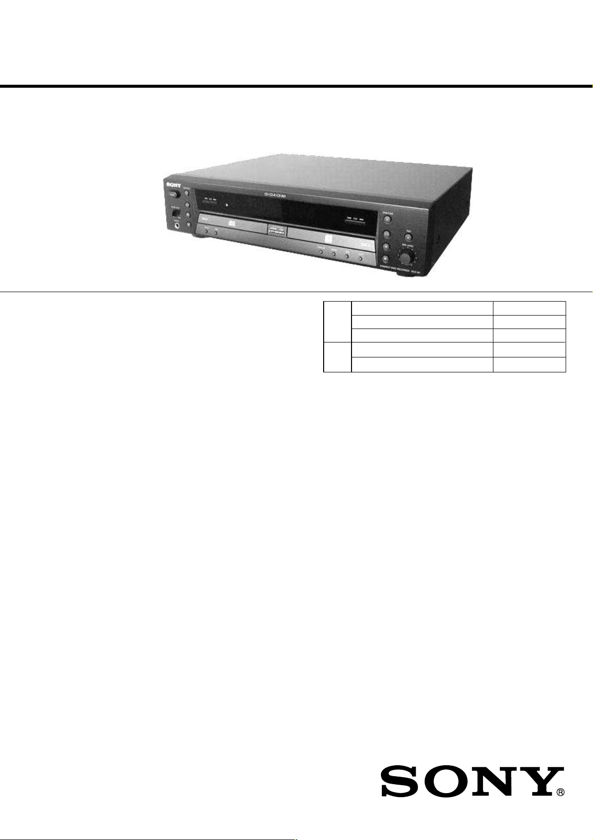
RCD-W1
SERVICE MANUAL
Ver 1.2 2001.08
SPECIFICATIONS
DECK A (the CD player section)
System Compact disc and digital
audio system
Laser Semiconductor laser ( λ =
780 nm)
Emission duration:
continuous
Frequency response 20Hz–20,000kHz (0.5
dB)
Signal-to-noise ratio More than 100 dB
Dynamic range More than 93 dB
DECK B (the CD-R and CD-RW
recording section)
System Compact disc digital audio
system
Laser Semiconductor laser ( λ =
780 nm)
Emission duration:
continuous
Playable discs CD, CD-R, CD-RW
Recordable discs CD-R, CD-RW (for music
use)
Frequency response 20 to 20,000 Hz ±0.5 dB
Signal-to-noise ratio Over 96 dB during
playback
Dynamic range More than 93 dB during
playback
US Model
Canadian Model
E Model
Model Name Using Similar Machanism NEW
CD-R
CD Mechanism Type CDM-700(CD-RW)
Optical Pick-up Type KRS-220C
Model Name Using Similar Mechanism NEW
CDP
CD Mechanism Type CDM-700(CDP)
Inputs
ANALOG IN
(Phono jacks) impedance 47 kilohms
Rated input 330 mVrms
Minimum input
125 mVrms
DIGITAL OPTICAL IN
(Square optical connector jack)
Optical wavelength
660 nm
Outputs
ANALOG OUT
(Phono jacks) impedance 47 kilohms
OPTICAL DIGITAL OUT
(Square optical connector jack)
General
Power requirements
U.S.A. and Canada 120 V AC, 60 Hz
Power consumption 28 W
Dimensions (approx.) (w/h/d) incl. projecting parts
Mass (approx.) 4.6 kg
Supplied accessories • Audio connecting cord (2)
Design and specifications are subject to change
without notice.
Rated output 2 Vrms
Load impedance over
10 kilohms
Wavelength 660 nm
Output level -18 dBm
and control
430 x 108 x 368 mm
• Remote commander (remote) (1)
• Size AA (R6) batteries (2).
9-929-582-13
2001H0200-1
© 2001.8
COMPACT DISC RECORDER
Sony Corporation
Home Audio Company
Shinagawa Tec Service Manual Production Group
RCD-W1
NOTES ON HANDLING THE OPTICAL PICK-UP
BLOCK OR BASE UNIT
The laser diode in the optical pick-up block may suffer electrostatic
break-down because of the potential difference generated by the
charged electrostatic load, etc. on clothing and the human body.
During repair, pay attention to electrostatic break-down and also
use the procedure in the printed matter which is included in the
repair parts.
The flexible board is easily damaged and should be handled with
care.
NOTES ON LASER DIODE EMISSION CHECK
The laser beam on this model is concentrated so as to be focused on
the disc reflective surface by the objective lens in the optical pickup block. Therefore, when checking the laser diode emission, observe from more than 30 cm away from the objective lens.
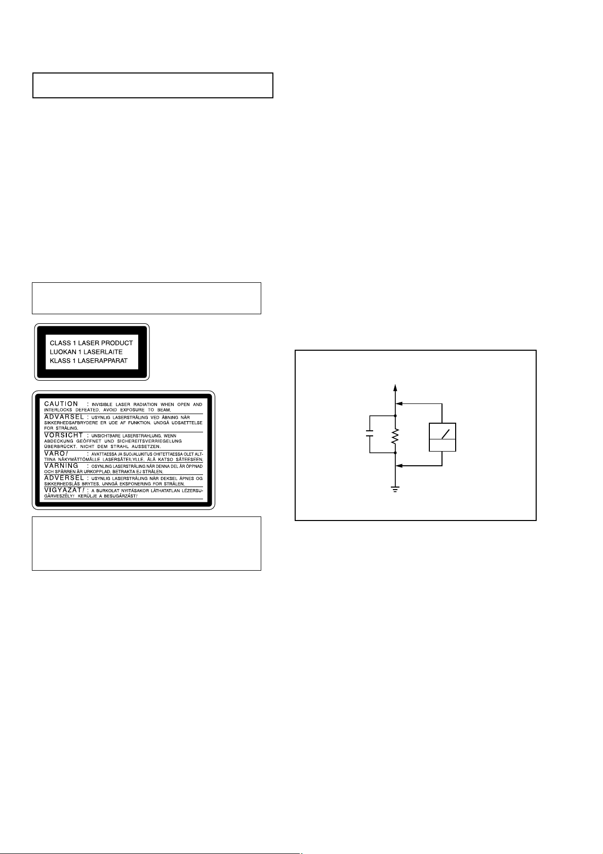
The Laser component in this product is capable of emitting
radiation exceeding the limit for Class 1.
This appliance is classified as
a CLASS 1 LASER product.
The CLASS 1 LASER PRODUCT MARKING is located on
the rear exterior.
SAFETY CHECK-OUT
(US model only)
After correcting the original service problem, perform the following safety checks before releasing the set to the customer:
Check the antenna terminals, metal trim, “metallized” knobs, screws,
and all other exposed metal parts for AC leakage. Check leakage as
described below.
LEAKAGE
The AC leakage from any exposed metal part to earth Ground and
from all exposed metal parts to any exposed metal part having a
return to chassis, must not exceed 0.5 mA (500 microampers). Leakage current can be measured by any one of three methods.
1. A commercial leakage tester, such as the Simpson 229 or RCA
WT-540A. Follow the manufacturers’ instructions to use these
instruments.
2. A battery-operated AC milliammeter. The Data Precision 245
digital multimeter is suitable for this job.
3. Measuring the voltage drop across a resistor by means of a VOM
or battery-operated AC voltmeter. The “limit” indication is 0.75
V, so analog meters must have an accurate low-voltage scale.
The Simpson 250 and Sanwa SH-63Trd are examples of a passive VOM that is suitable. Nearly all battery operated digital
multimeters that have a 2V AC range are suitable. (See Fig. A)
To Exposed Metal
Parts on Set
This caution
label is located
inside the unit.
CAUTION
Use of controls or adjustments or performance of procedures
other than those specified herein may result in hazardous radiation exposure.
Notes on chip component replacement
• Never reuse a disconnected chip component.
• Notice that the minus side of a tantalum capacitor may be
damaged by heat.
Flexible Circuit Board Repairing
• Keep the temperature of soldering iron around 270˚C
during repairing.
• Do not touch the soldering iron on the same conductor of the
circuit board (within 3 times).
• Be careful not to apply force on the conductor when soldering
or unsoldering.
SAFETY-RELATED COMPONENT WARNING !!
COMPONENTS IDENTIFIED BY MARK ! OR DOTTED LINE
WITH MARK ! ON THE SCHEMATIC DIAGRAMS AND IN
THE PARTS LIST ARE CRITICAL TO SAFE OPERATION.
REPLACE THESE COMPONENTS WITH SONY PARTS
WHOSE PART NUMBERS APPEAR AS SHOWN IN THIS
MANUAL OR IN SUPPLEMENTS PUBLISHED BY SONY.
0.15µF
1.5kΩ
Earth Ground
AC
voltmeter
(0.75V)
Fig. A. Using an AC voltmeter to check AC leakage.
ATTENTION AU COMPOSANT AYANT RAPPORT
À LA SÉCURITÉ!!
LES COMPOSANTS IDENTIFIÉS PAR UNE MARQUE ! SUR
LES DIAGRAMMES SCHÉMATIQUES ET LA LISTE DES
PIÈCES SONT CRITIQUES POUR LA SÉCURITÉ DE
FONCTIONNEMENT. NE REMPLACER CES COMPOSANTS
QUE PAR DES PIÈCES SONY DONT LES NUMÉROS
SONT DONNÉS DANS CE MANUEL OU DANS LES
SUPPLÉMENTS PUBLIÉS PAR SONY.
2

RCD-W1
Error Messages
The following table explains the error messages
that appear in the display.
Message
CHECK DISC
DATA DISC
DISC ERROR
DISC FULL
ERROR
FAILED
FULL
NO AUDIO
Explanation
• A record-related button has been
pressed when a finalized disc is in
the DECK B.
• A record-related button has been
pressed when a standard CD is in
the DECK B.
A non-audio CD-ROM or a CDVideo disc has been placed in the
machine.
• An unfinalized disc has been
placed in the DECK A.
• A DVD disc has been placed in
the unit.
There is not enough time left on the
disc to complete a planned
recording.
• The disc is not seated properly.
• There is a problem with the disc.
A dubbing has not been completed
properly.
More than 20 tracks have been
programmed.
A record-related button has been
pressed when a non-audio disc is in
the DECK B.
TABLE OF CONTENTS
1. SERVICING NOTE .......................................................... 4
2. GENERAL .......................................................................... 8
3. DISASSEMBLY
3-1. Top Case ............................................................................... 9
3-2. Tray Door, Front Panel Assy .............................................. 10
3-3. HP board, FL board, VOL board ........................................ 10
3-4. Back Panel ......................................................................... 11
3-5. Audio Board ....................................................................... 11
3-6. Power Board ...................................................................... 12
3-7. CDP Deck assy (Deck A), CD-R Deck Assy (Deck B) ..... 12
3-8. BD Board (Deck A) ........................................................... 13
3-9. CDP Mechanism Assy (Deck A) ........................................ 13
3-10.Spindle Motor Assy, Pick-Up Block (Deck A) .................. 14
3-11.BD-R Board........................................................................ 14
3-12.CD-R Mechanism Assy (Deck B) ...................................... 15
3-13.Sled Mechanism Assy ........................................................ 15
4. ELECTRICAL ADJUSTMENT ................................... 16
5. DIAGRAMS
5-1. Circuit Boards Location .................................................... 23
5-2. Block diagrams – CD-R Section (1/2) – ........................... 25
Block diagrams – CD-R Section (2/2) – ........................... 26
Block diagrams – CDP Section – ...................................... 27
Block diagrams – Audio Section – ................................... 28
Block diagrams – Power Section – ................................... 29
5-3. Printed Wiring Board – CD-R Section (Side A) – ............ 30
Printed Wiring Board – CD-R Section (Side B) – ............ 31
5-4. Schematic Diagram – CD-R Section (1/6) – ..................... 32
5-5. Schematic Diagram – CD-R Section (2/6) – ..................... 33
5-6. Schematic Diagram – CD-R Section (3/6) – ..................... 34
5-7. Schematic Diagram – CD-R Section (4/6) – ..................... 35
5-8. Schematic Diagram – CD-R Section (5/6) – ..................... 36
5-9. Schematic Diagram – CD-R Section (6/6) – ..................... 37
5-10. Printed Wiring Board – CDP Section (Side A) – .............. 38
Printed Wiring Board – CDP Section (Side B) – ............... 39
5-11. Schematic Diagram – CDP Section (1/3)– ....................... 40
5-12. Schematic Diagram – CDP Section (2/3)– ....................... 41
5-13. Schematic Diagram – CDP Section (3/3)– ....................... 42
5-14. Schematic Diagram – Audio Section (1/2)–..................... 43
5-15. Schematic Diagram – Audio Section (2/2)–..................... 44
5-16. Printed Wiring Board – Audio Section – ........................... 45
5-17. Printed Wiring Board – Panel Section –........................... 46
5-18. Schematic Diagram – Panel Section – ............................. 47
5-19. Printed Wiring Board – Power Section – ......................... 48
5-20. Schematic Diagram – Power Section – ............................ 49
5-21. IC Pin Functions ............................................................... 50
5-22. IC Block Diagrams ........................................................... 55
6. EXPLODED VIEWS
6-1. Front Panel Section ............................................................. 61
6-2. Chassis Section ................................................................... 62
6-3. CD Play Section (Deck A) .................................................. 63
6-4. CD Record Section ............................................................. 64
7. ELECTRICAL PARTS LIST ................................. 65
3
RCD-W1
SECTION 1
SERVICING NOTE
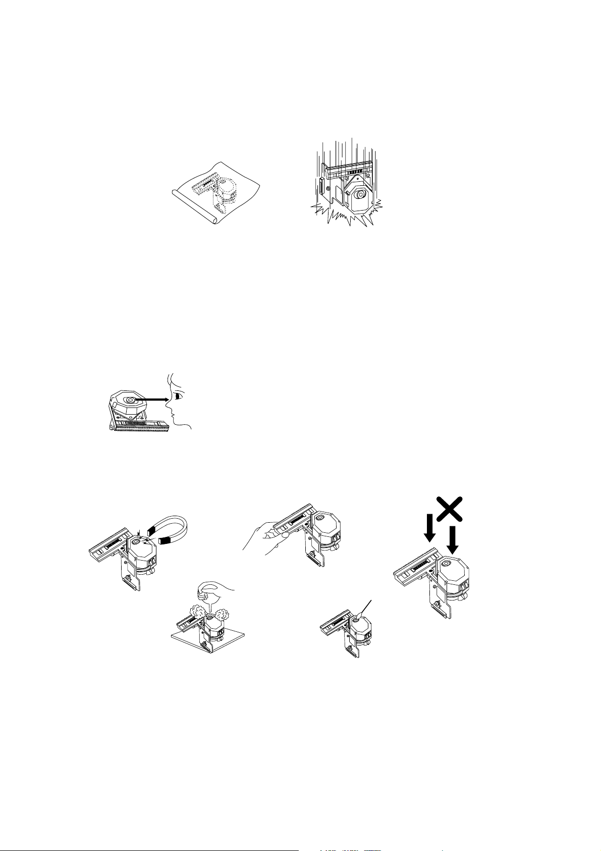
NOTES REGARDING HANDLING OF THE PICK-UP
1. Notes for transport and storage
1) The pick-up should always be left in its conductive bag until immediately prior to use.
2) The pick-up should never be subjected to external pressure or impact.
Storage in conductive bag
Drop impact
2. Repair notes
1) The pick-up incorporates a strong magnet, and so should never be brought close to magnetic materials.
2) The pick-up should always be handled correctly and carefully , taking care to avoid external pressure and impact.
If it is subjected to pressure or impact, the result may be an operational malfunction and/or damage to the
printed-circuit board.
3) Each and every pick-up is already individually adjusted to a high degree of precision, and for that reason the
adjustment point and installation screws should absolutely never be touched.
4) Laser beams may damage the eyes!
Absolutely never permit laser beams to enter the eyes!
Also NEVER switch ON the power to the laser output part (lens, etc.) of the pick-up if it is damaged.
NEVER look directly at the laser beam, and don’t let contact
fingers or other exposed skin.
5) Cleaning the lens surface
If there is dust on the lens surface, the dust should be cleaned away by using an air bush (such as used for
camera lens). The lens is held by a delicate spring. When cleaning the lens surface, therefore, a cotton swab
should be used, taking care not to distort this.
Pressure
Magnet
How to hold the pick-up
Cotton swab
Conductive Sheet
6) Never attempt to disassemble the pick-up.
Spring by excess pressure. If the lens is extremely dirty, apply isopropyl alcohol to the cotton swab. (Do not use any
other liquid cleaners, because they will damage the lens.) Take care not to use too much of this alcohol on the swab,
and do not allow the alcohol to get inside the pick-up.
Pressure
4
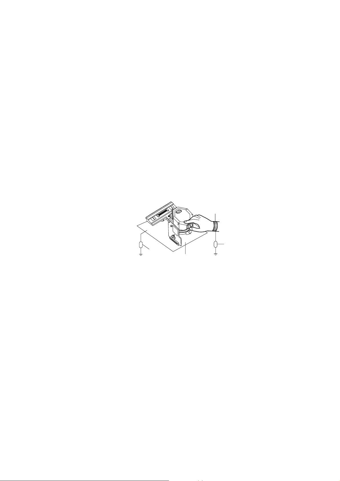
NOTES REGARDING COMPACT DISC PLAYER REPAIRS
1. Preparations
1) Compact disc players incorporate a great many ICs as well as the pick-up (laser diode). These components are sensitive to, and easily affected by, static electricity. If such static is high voltage, components
can be damaged, and for that reason components should be handled with care.
2) The pick-up is composed of many optical components and other high-precision components. Care must
be taken, therefore, to avoid repair or storage where the temperature of humidity is high, where strong
magnetism is present, or where there is excessive dust.
2. Notes for repair
1) Before replacing a component part, first disconnect the power supply lead wire from the unit
2) All equipment, measuring instruments and tools must be grounded.
3) The workbench should be covered with a conductive sheet and grounded.
When removing the laser pick-up from its conductive bag, do not place the pick-up on the bag. (This is
because there is the possibility of damage by static electricity.)
4) To prevent AC leakage, the metal part of the soldering iron should be grounded.
5) Workers should be grounded by an armband (1MW)
6) Care should be taken not to permit the laser pick-up to come in contact with clothing, in order to prevent
static electricity changes in the clothing to escape from the armband.
7) The laser beam from the pick-up should NEVER be directly facing the eyes or bare skin.
RCD-W1
Resistor
(1MW )
Conduct
Sheet
Armband
Resistor
(1MW)
ive
5

RCD-W1
Electrostatically Sensitive Devices (ESD)
Some semiconductor (solid state) devices can be damaged easily by static electricity. Such components commonly are called Electrostatically Sensitive Devices (ESD). Examples of typical ESD devices are integrated circuits and some field-effect transistors and semiconductor chip components. The following techniques should
be used to help reduce the incidence of component damage caused by static electricity.
1. Immediately before handling any semiconductor component or semiconductor-equipped assembly, drain off
any electrostatic charge on your body by touching a known earth ground. Alternatively, obtain and wear a
commercially available discharging wrist strap device, which should be removed for potential shock reasons
prior to applying power to the unit under test.
2. After removing an electrical assembly equipped with ESD devices, place the assembly on a conductive surface such as aluminum foil, to prevent electrostatic charge buildup or exposure of the assembly.
3. Use only a grounded-tip soldering iron to solder or unsolder ESD devices.
4. Use only an anti-static solder removal device. Some solder removal devices not classified as "anti-static" can
generate electrical charges sufficient to damage ESD devices.
5. Do not use freon-propelled chemicals. These can generate electrical charges sufficient to damage ESD devices.
6. Do not remove a replacement ESD device from its protective package until immediately before you are ready
to install it. (Most replacement ESD devices are packaged with leads electrically shorted together by conductive
foam, aluminum foil or comparable conductive materials).
7. Immediately before removing the protective material from the leads of a replacement ESD device, touch the
protective material to the chassis or circuit assembly into which the device will by installed.
CAUTION : BE SURE NO POWER IS APPLIED TO THE CHASSIS OR CIRCUIT, AND OBSERVE ALL
OTHER SAFETY PRECAUTIONS.
8. Minimize bodily motions when handing unpackaged replacement ESD devices. (Otherwise harmless motion
such as the brushing together of your clothes fabric or the lifting of your foot from a carpeted floor can gen erate static electricity sufficient to damage an ESD device).
6
RCD-W1
)
NOTE ON CHECKING POWER SUPPLY CIRCUIT
1. When check the primary part, you must remove the GND pin of
the scope and soldering machine.
Primary GND : C903 – terminal at power board.
2. When check the primary part, you must open the another GND(not
used GND) of scope.
(If another scope GND is connected to secondary GND or other
system, input power line or system have some damage.)
3. When touch the primary part by hand in defected system,
if you use the power line switch, remove the power cord and then
check or touch.
Because in general power switch is switching only one line.
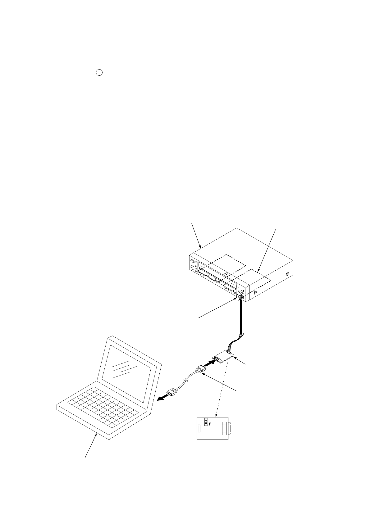
BD-R BOARD CHECK AND ADJUSTING JIGS
In case of checking or adjusting the LD power of BD-R board, the PC connection jig (J-2501-210-A) and the test program are required.
This test program is distributed with the service manual.
4. When check the primary part, after remove power cord and dis
charge the primary capacitor, and then check the system.
In the normal state, the voltage of the capacitor is small
(about 10V), but in the abnormal state is very high ( about 140V
at 100V A.C or 300V at 220V).
When discharge the capacitor, use the wattage resistor(about 100
ohm).
5. In the narrow system, Until set repaired completely,
insert the power cord at the moment repeatedly and then check
the waveform.
6. In the wide system, when insert the power cord, check the wave
form after about 3 second.
Because the wide system is the soft start method.
RCD-W1
CD-R
test connector (PN201)
BD-R board
PC connection jig
(J-2501-210-A)
PS-232C cable (D-sub 9pin
(straight type)
PC
SW501
W
D
CNP501CN505
PC connection jig
Set SW501 to “D” side
7
RCD-W1
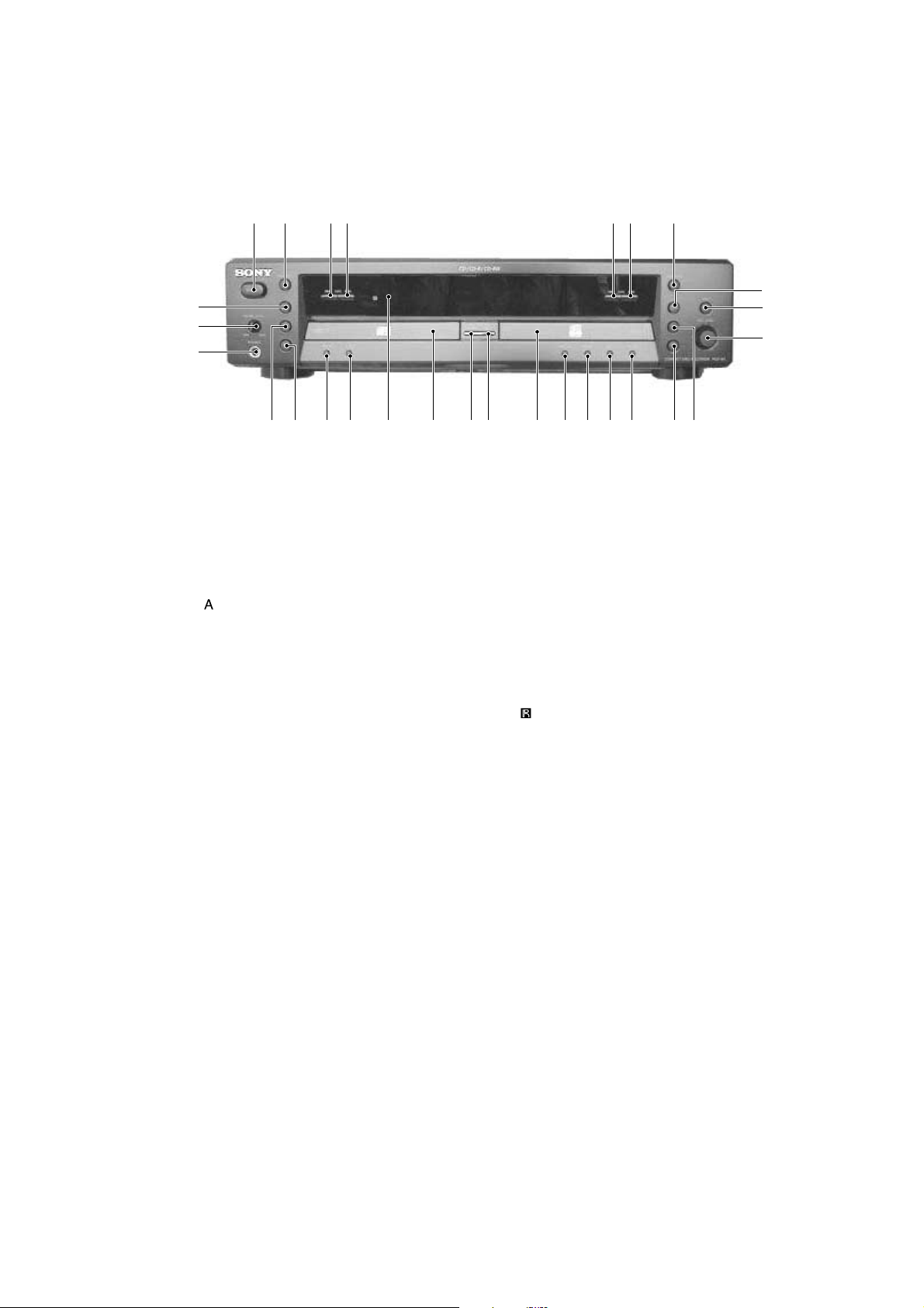
FRONT PANEL
wk
wj
wh
SECTION 2
GENERAL
21 34 56 7
8
9
0
LOCATION OF PARTS AND CONTROLS
1 Power button
2 OPEN/CLOSE A button (DECK A)
3 . AMS button (DECK A)
4 > AMS button (DECK A)
5 . AMS button (DECK B)
6 > AMS button (DECK B)
7 OPEN/CLOSE A button (DECK B)
8 H button (DECK B)
9 z REC button
q; REC LEVEL knob (DECK B)
qa X button (DECK B)
qs x button (DECK B)
qd INPUT button (DECK B)
qf TIME button (DECK B)
wa w; qlqkwd wswfwg
qj qgqh qd qsqf
qg ERASE button (DECK B)
qh FINALIZE button (DECK B)
qj DISC tray (DECK B)
qk CD SYNCHRO HIGH button
ql CD SYNCHRO NORMAL button
w; DISC tray (DECK A)
remote sensor
wa
ws TIME button (DECK A)
wd RELAY button (DECK A)
wf x button (DECK A)
wg X button (DECK A)
wh PHONE jack
wj PHONE LEVEL knob
wk H button (DECK A)
qa
8
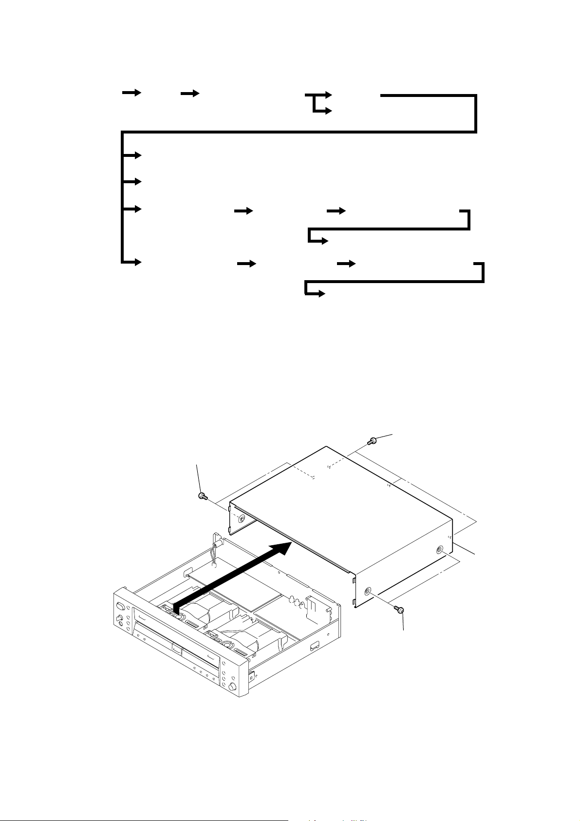
Note: Disassemble the unit in the order as shown below.
RCD-W1
SECTION 3
DISASSEMBLY
Set
Note: Follow the disassembly procedure in the numerical order given.
Top case
Audio board
Power board
CDP deck assy (deck A)
CD-R deck assy (deck B)
Tray door, Front panel assy
BD board (deck A)
BD-R board (deck B)
3-1. TOP CASE
Back panel
HP board, FL board, VOL board
CDP mechanism assy (deck A)
Spindle motor assy, Pick-up block (deck A)
CD-R mechanism assy (deck B)
Sled mechanism assy
1
Two screws (case)
3
2
Three screws (case)
1
Two screws (case)
4
Top case
9
RCD-W1
)
)
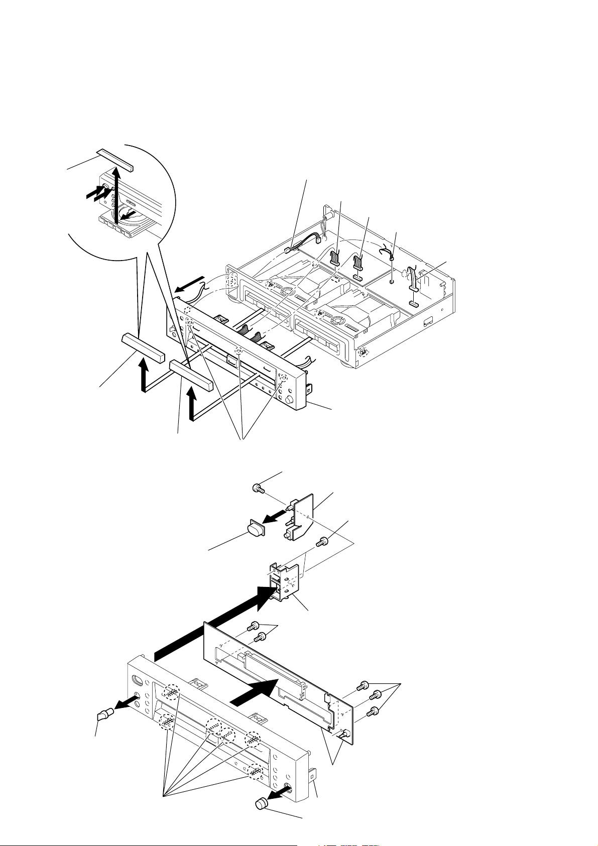
3-2. TRAY DOOR, FRONT PANEL ASSY
Note:After No.2 removal, remove in the state power turns off.
1
Turn power on by pressing POWER button in the drrow
direction and press OPEN/CLOSE button in the drrow
to open the tray.
Then remove the tray door in the drow
(In the case of DECK B, remove it in the same manner.)
C
direction.
A
B
Tray door
A
C
B
Tray door (Play)
(deck A)
8
Tray door (Rec)
(deck B)
7
Claws
6
Connector (PN901)
5
Connector (PN603)
9
Front panel assy
4
Connector (PN904)
3
Connector (PN401)
2
Connector (PN501
3-3. HP BOARD, FL BOARD, VOL BOARD
6
POWER knob
4
2
P/VOLUME knob
7
Screw (Special)
8
5
PWB holder
0
Two screws (Special)
HP board
3
Two screws (Special)
9
Four screws (Special
10
qa
Claws
qs
FL board and VOL board
Front panel
1
REC VOL knob
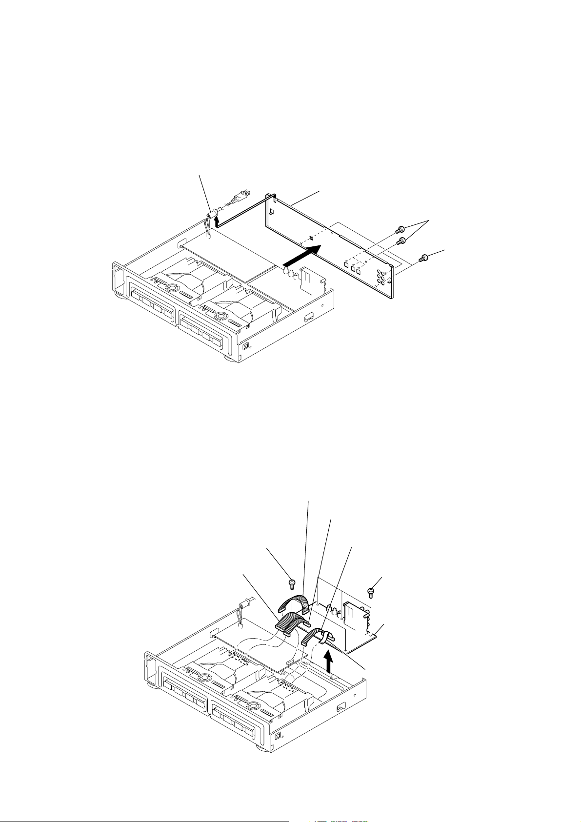
3-4. BACK PANEL
)
)
3
Cord power
4
5
Back panel
1
Four screws (3X10)
2
Two screws (3X8 BK
RCD-W1
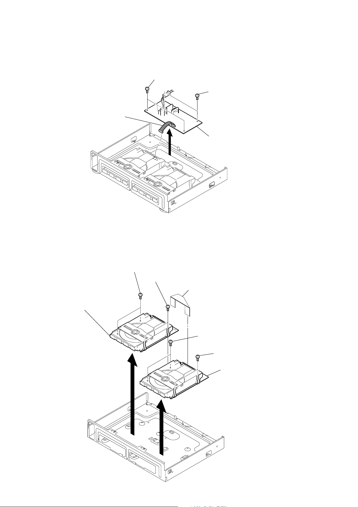
3-5. AUDIO BOARD
6
Two screws (special)
4
Connector (PN606)
5
Connector (PN201)
3
Connector (PN602)
2
Connector (PN105)
8
7
Three screws (special
9
AUDIO board
1
Wire (flat type) (CN102)
11
RCD-W1
)
)
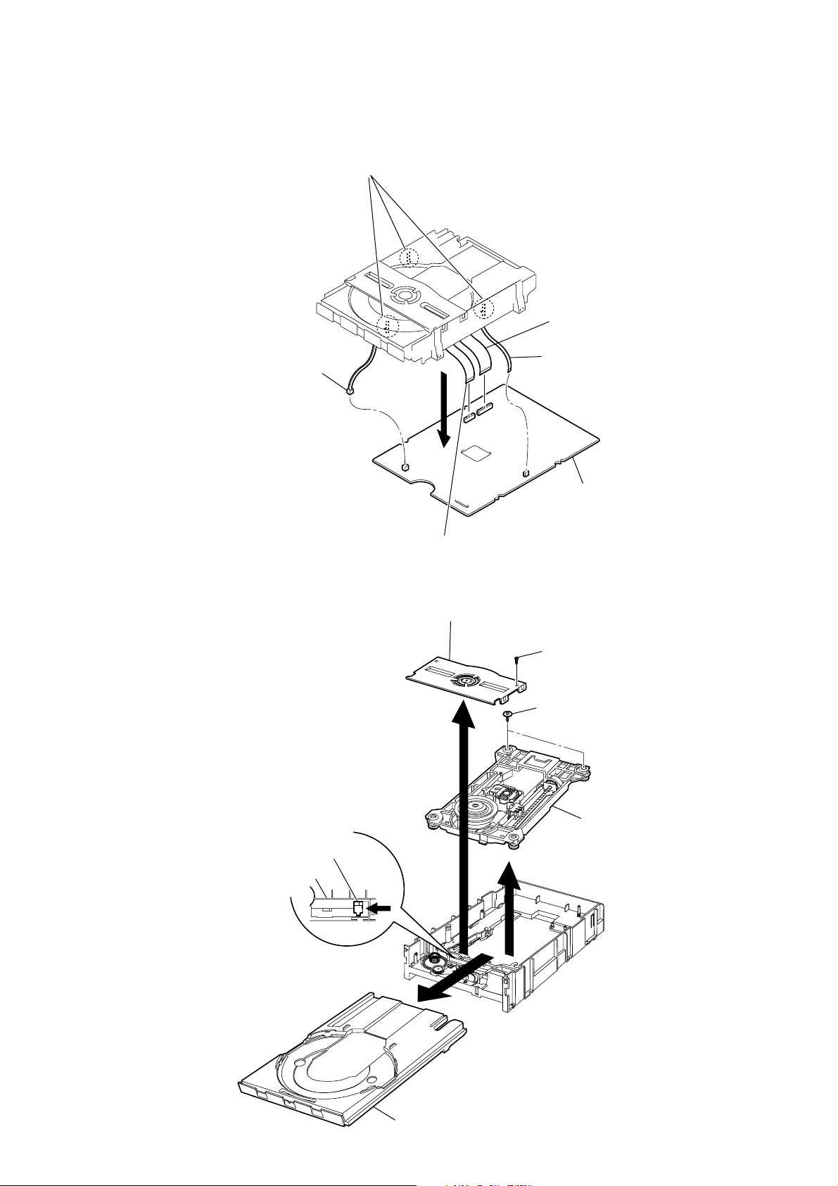
3-6. POWER BOARD
1
Connector (PN601)
2
Two screws (special)
4
3
Two screws (special
5
POWER board
3-7. CDP DECK ASSY (DECK A), CD-R DECK ASSY (DECK B)
2
Two screws (special)
3
Two screws (special)
5
CDP deck assy (deck A)
4
8
1
Wire (flat type)(PN605)
6
Two screws (special)
7
Two screws (special)
9
CD-R deck assy (deck B
12
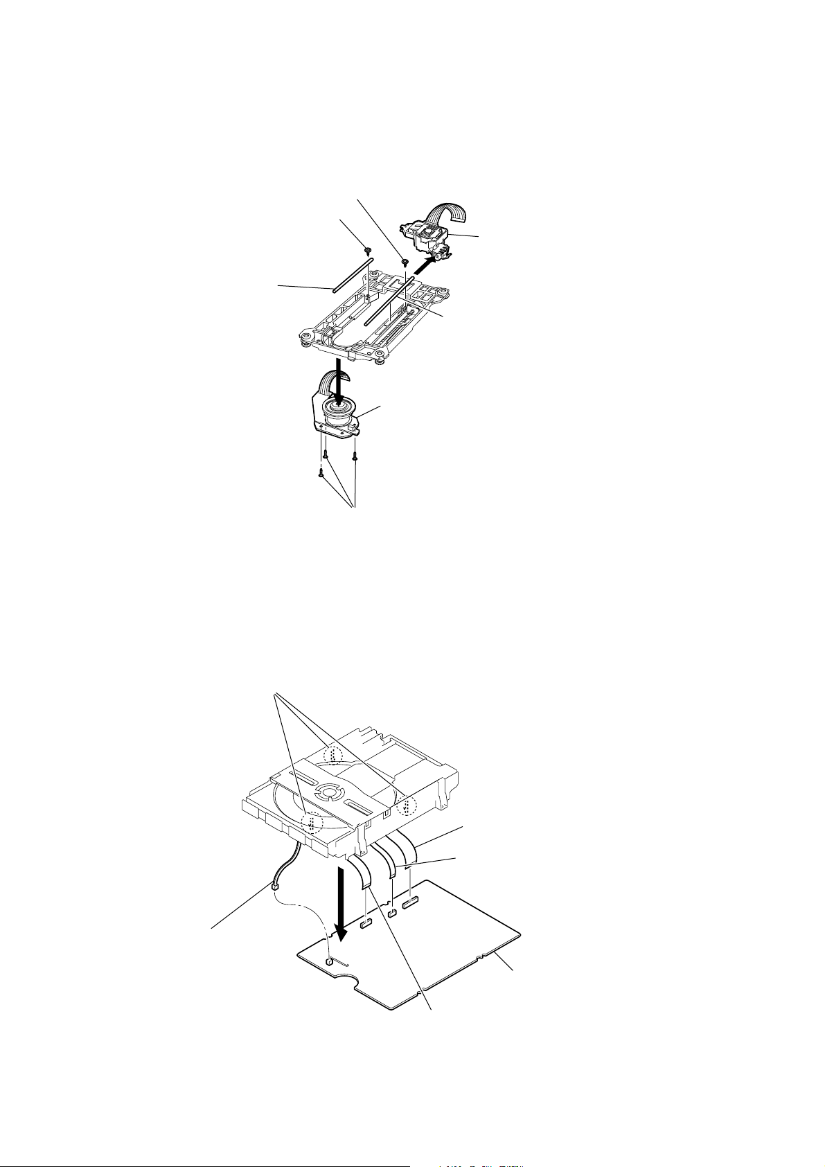
3-8. BD BOARD (DECK A)
y
)
3
Connector (PN609)
1
Three claws
6
4
Wire (flat type) (PN201
2
Wire (flat type) (PN301)
RCD-W1
3-9. CDP MECHANISM ASSY (DECK A)
4
Push out the disc tray by pushing the
Up/Down guide un the drrow
Up/Down guide
Main base
A
direction.
A
5
Wire (flat type) (PN401)
3
Clamp holder assy
7
2
8
BD board
1
Screw (1.7X6)
Two screws
9
CDP mechanism ass
Bottom view
6
Disc tray
5
13
RCD-W1
k
3-10. SPINDLE MOTOR ASSY, PICK-UP BLOCK (DECK A)
5
Screw (1.7X5)
3
Screw (1.7X5)
8
Pick-up bloc
3-11. BD-R BOARD (DECK B)
4
Shaft L
2
Spindle motor assy
1
Three screws (2X6)
7
6
Shaft R
2
Connector (CN701)
1
Three claws
6
3
Wire (fiat type) (CN401)
4
Wire (fiat type) (CN501)
7
BD-R board
5
Wire (flat type) (CN502)
14
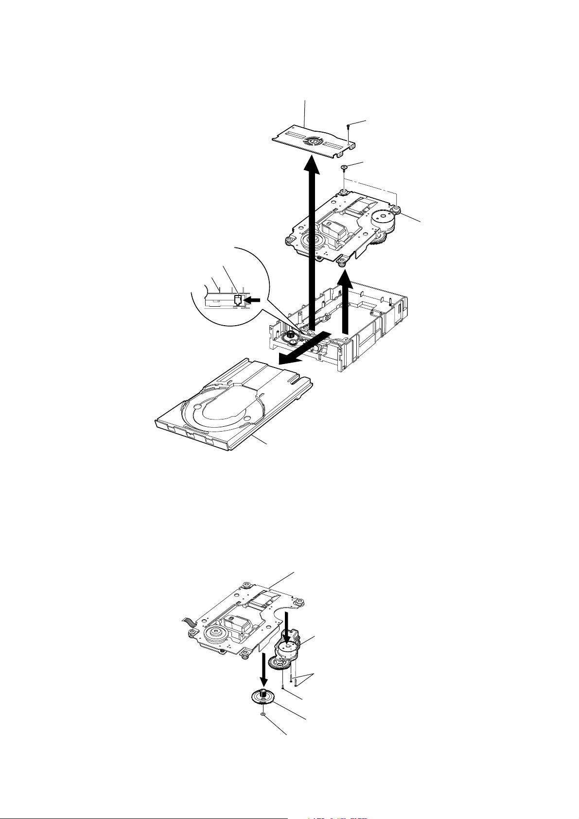
3-12. CD-R MECHANISM ASSY (DECK B)
y
4
Push out the disc tray by pushing the
Up/Down suide un the drrow
Up/Down guide
Main base
A
direction.
A
3
Clamp holder assy
2
1
7
8
Two screws
Screw (1.7X6)
9
CD-R mechanism ass
RCD-W1
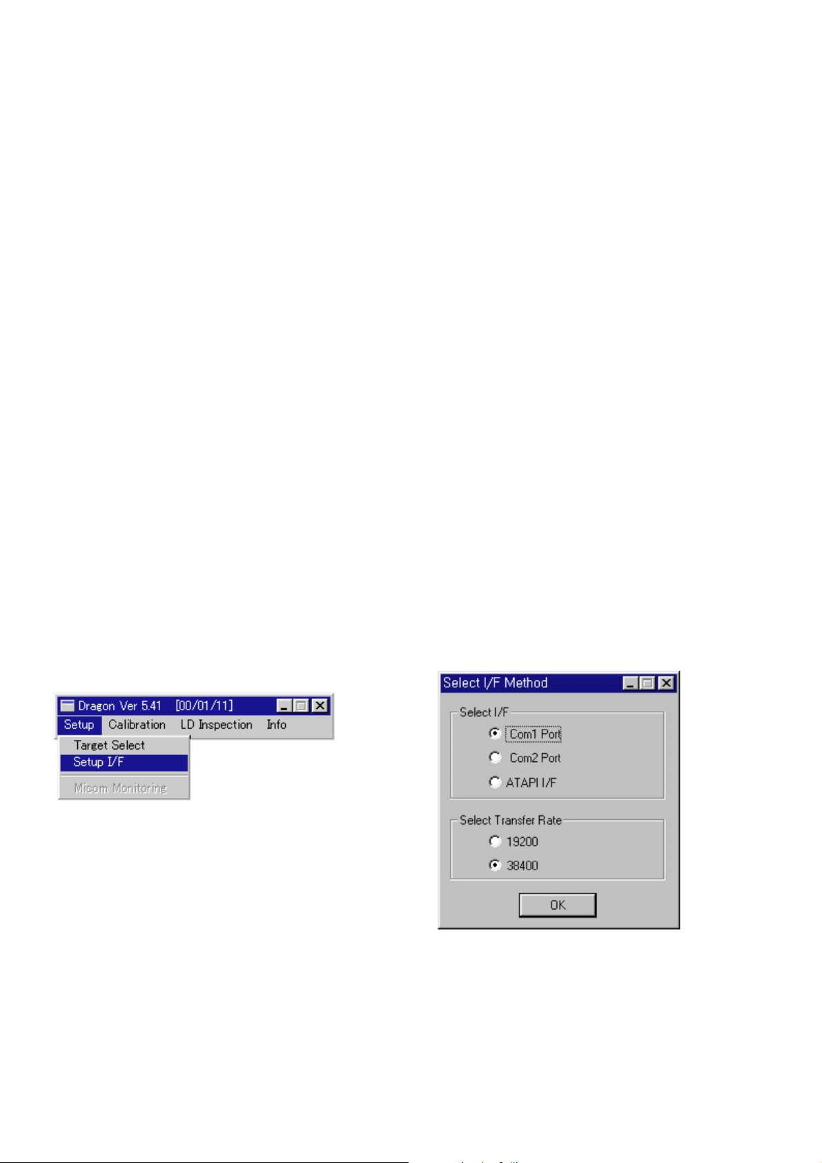
3-13. SLED MECHANISM ASSY
Bottom view
6
Disc tray
5
CD-R mechanism assy
3
Screw (2.0x4.5)
2
Washer
1
5
Sled mechanism assy
4
Two screws (2.0x11.5)
Pinion gear assy
15
RCD-W1
SECTION 4
ELECTRICAL ADJUSTMENT
LD Power Adjustment
Jigs used on this adjustment
• LD Power Meter
A laser power meter 10mW or more measurable is required. Don’t use the laser power meter for Mini disc because of 10mW max.
Optical power meter (TQ8210): Product of ADVANTEST (on the market).
A thin type optical sensor (Q82017A): Product of ADVANTEST (on the market).
• PC Connection Jig (J-2501-210-A)
• Test Program FD
Dragon program Ver. 5.41
(This test program is distributed with the service manual.)
• PC (Windows 95/98)
• RS-232C Cable (on the market) D-SUB 9 pin, straight type
• Test Disc for Operation Check
A low reflecting rate disc for checking playback performance. OK: It can be played back.
• Low reflecting CD-R disc: TCD-R082LMT (J-2502-063-1)
• Low reflecting CD-RW disc: TCD-W082L (J-2502-063-2)
Laser Power Adjustment (CD-R Only)
In case of the following parts are replaced, this adjustment is required.
1. CD-R optical pick-up block (KRS-220C)
2. IC702 (EP- ROM)
Specification of Dragon Program Usage Environment
The Dragon Program programmed by API function of Windows 95 can be surely operated on the Windows 95/98 platform.
It isn’t guaranteed on the other platform.
Start up
Procedure:
1. Connect the PC connection jig with the RS-231C cable between the test connector (PN201) on CD-R of RCD-W1 and COM port on PC.
(Check SW501 on the PC connection jig to “D” side.)
2. Turn power on RCD-W1.
3. Execute Dragon.exe on Windows.
(Two files Dragon.exe and dragon.cfg are displayed on the setup menu window.)
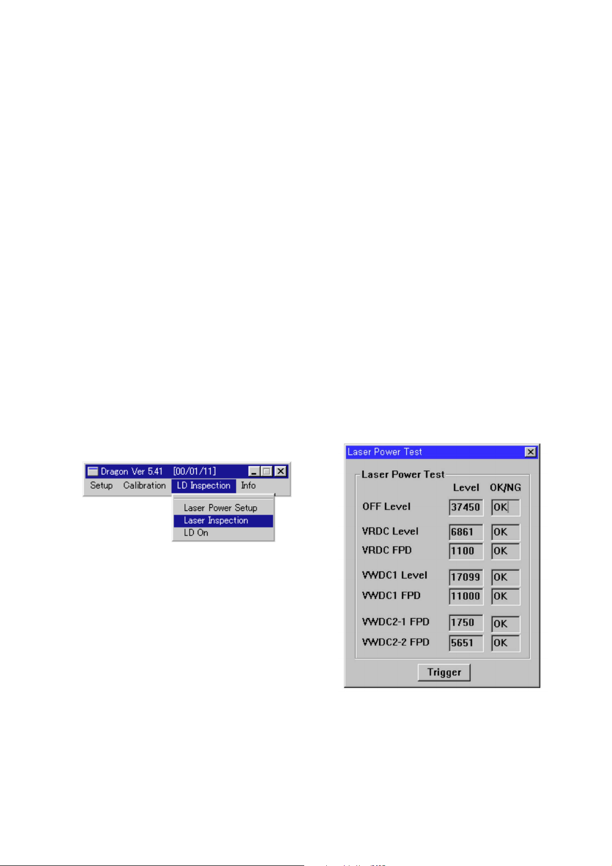
4. Select “Setup I/F” on “Setup” pull-down menu, then “Select I/F Method” window is open.
5. Select Com Port matching to the Com Port connected the PC connection jig.
6. Select “38400” of “Select Transfer Rate”.
7. Click OK.
Fig 1 : Dragon menu and setup menu windows
16
Fig 2 : Select I/F method window
RCD-W1
CD-R LD Setting Check
(VRDC/VWDC/FPD Level Value Check)
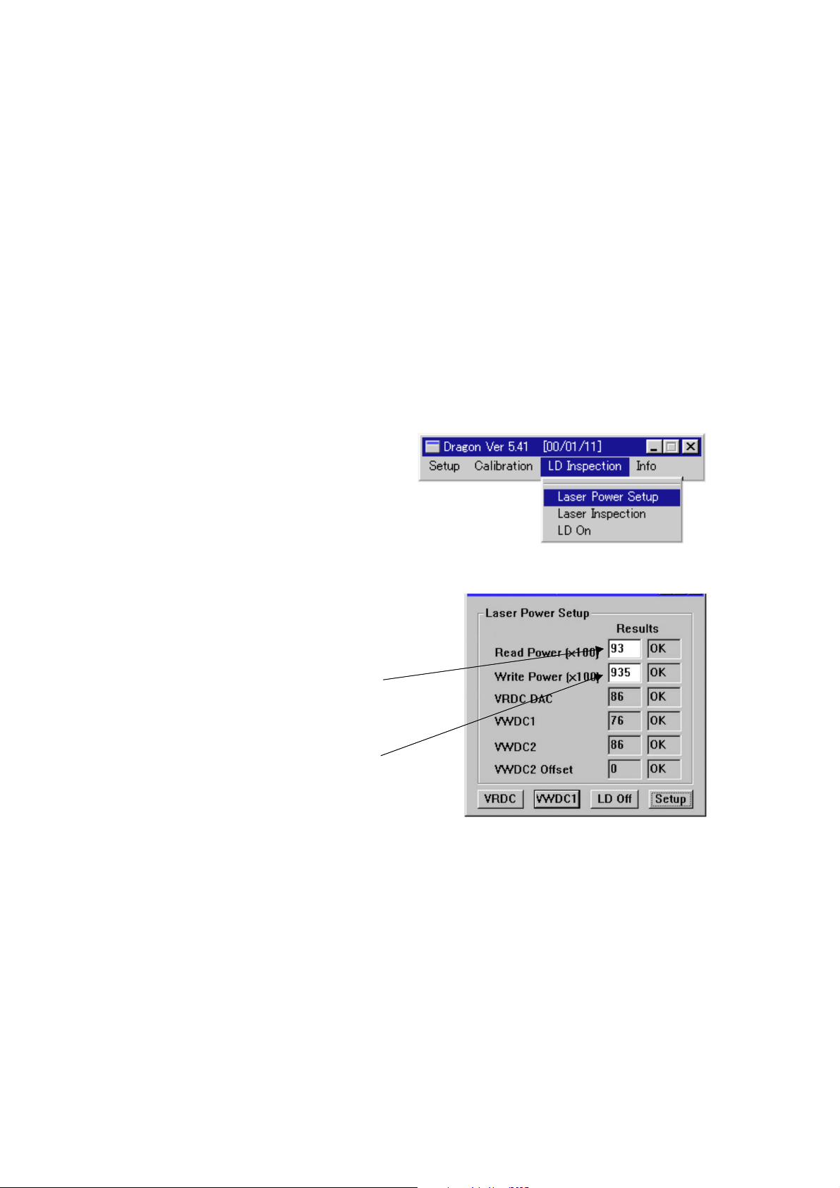
This routine is for checking performances of the record/playback D-A converter (IC409), RFIC (IC413), the encoder/decoder IC
(IC401), CPLD (IC601), the optical pick-up block (KRS-220C), the microcomputer(IC701) and so on.
It diagnoses malfunctions of interface, the pick-up or so on.
It diagnoses the circuit in the recording mode without disc.
Description of each item
OFF LEVEL: In case of the laser turns off, FPDO output is 3V. Sampling value at this time.
VRDC LEVEL: APC circuit VRDC signal sampling value after READ power setting.
VRDC FPD: Optical pick-up FPDO signal sampling value after READ power setting.
VWDC1 LEVEL:APC circuit VWDC signal sampling value after setting WRITE power to regular value.
VWDC1 FPD: Optical pick-up FPDO signal sampling value after setting WRITE power to regular value.
VWDC2-1 FPD: There are two types of characteristics because of a non-linearity period of laser diode in the
over drive portion. This is FPDO sampling value in case of setting one of them to VWDC2 value.
VWDC2-2 FPD: FPDO sampling value in case of setting the other to VWDC2 value.
Specification of each item
38400-3300<OFF_LEVEL<38400+3300 (3.0±0.25V)
10<VRDC_LEVEL<20000
880<VRDC_FPD<1320
2000<VWDC1_LEVEL<25000
8640<VWDC1_FPD<12960
10<VWDC2-1_FPD<9500
2000<VWDC2-2_FPD<16000
Procedure:
1. Eject a disc from CD-R.
2. Select “Laser Inspection” on “LD Inspection” pull-down menu, then “Laser Power Test” window is open.
3. Click Trigger to execute LD check.
4. LD checked results are displayed.
(“OK”/“NG” is displayed for every items.)
5. Click X to close “Laser Power Test” window.
Fig 3 : LD inspection menu windows
Fig 4 : Laser power test window
17
RCD-W1
CD-R LD Power Setting
(VRDC/VWDC1 Resetting)
The optical pick-up and ICs in the circuit have a characteristics individually. In this routine, the parameters related to the
recording/playback power are actually measured and set properly.
The parameters are VRDC, VWDC1, VWDC2, VWDC2 Offset and so on. The reading power and playback power are set
properly by computing the related parameters on the basis of actually measuring values.
The preset parameters are used on power setting in case of performing Read/Write CD-R, CD-RW and so on.
Actual operation: The microcomputer receives serial data, then executes the related performances, and send parameter values to PC.
PC checks its related parameters and judges OK/NG.
Description of each parameter
VRDC: Used on the Read Power setting in case of
reading CD-RW and CD-R. (DAC value on 100mW.)
VWDC: There is VWDC1 (Write power) pin in the optical pick-up block. The recording power is set by it and VWDC2
(Over drive) pin. Used on setting VWDC1 pin power on recording. (Unit: DAC value/10mW)
VWDC2: Used on setting VWDC2 (Over drive) pin power on recording. (Unit: DAC value/5mW)
VWDC2 Offset: Used on setting VWDC2 (Over drive) pin power with VWDC2 parameter on recording. (Unit: DAC value)
Specification of each parameter
20<read power<200
100<write power<2000
30<VRDC<150
48<VWDC1<150
50<VWDC2<126
VWDC2 Offset<35
Procedure:
1. Eject a disc from CD-R.
2. Select “Laser Power Setup” on “LD Inspection” pull-down
menu, then “Laser Power Setup (Manual)” window is open.
3. Click VRDC, then Pick-up moves outward and LD turns on.
4. Measure the LD power with a LD power meter. Write its value
to the blank of “Read Power” column.
(Write a value to two decimal places. Ex: Write “93” in case of
0.93mW.)
5. Click VWDC1, then LD turns on.
6. Measure the LD power with a LD power meter. Write its value
to the blank of “Write Power” column.
(Write a value to two decimal places. Ex: Write “1234” in case
of 12.34mW.)
7. Click LD Off to turn LD off.
8. Click Setup, then setting is over and a result is displayed.
(“OK”/“NG” is displayed for every items.)
9. Click X to close “Laser Power Setup (Manual)” window.
Fig 5 : LD inspection menu windows
Fig 6 : Laser power setup window
18
Adjustment Data Check
Check if the error has occurred on reading “CD-R LD POWER SETTING” value.
Procedure:
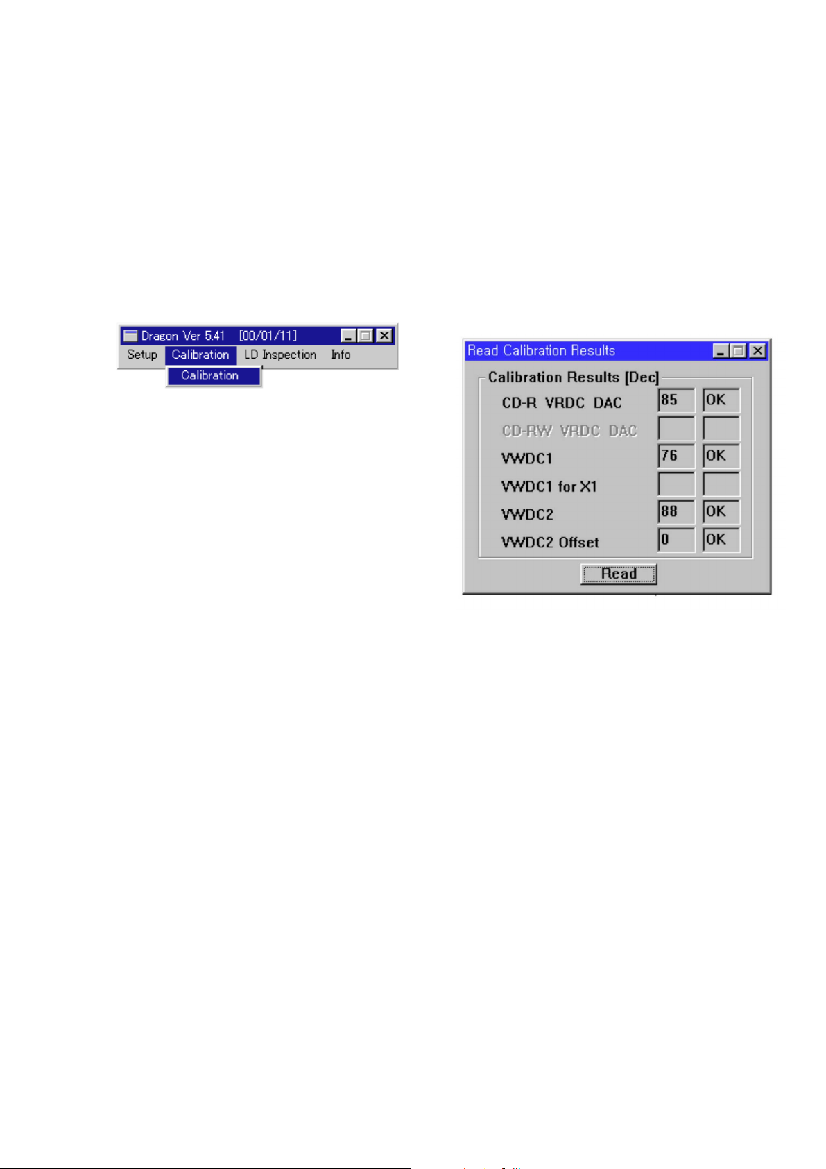
1. Select “Calibration” on “Calibration” pull-down menu, then “Read Calibration Results” window is open.
2. Click Read, then the calibration data are displayed.
3. Data specification
CD-R VRDC DAC: 30-150
VWDC1: 48-150
VWDC2: 50-126
VWDC2 Offset: 0-35
4. Click X to close “Read Calibration Results” window.
Fig 7 : Calibration menu windows
RCD-W1
Fig 8 : Read calibration results window
19
RCD-W1
)
e
SERVO Check
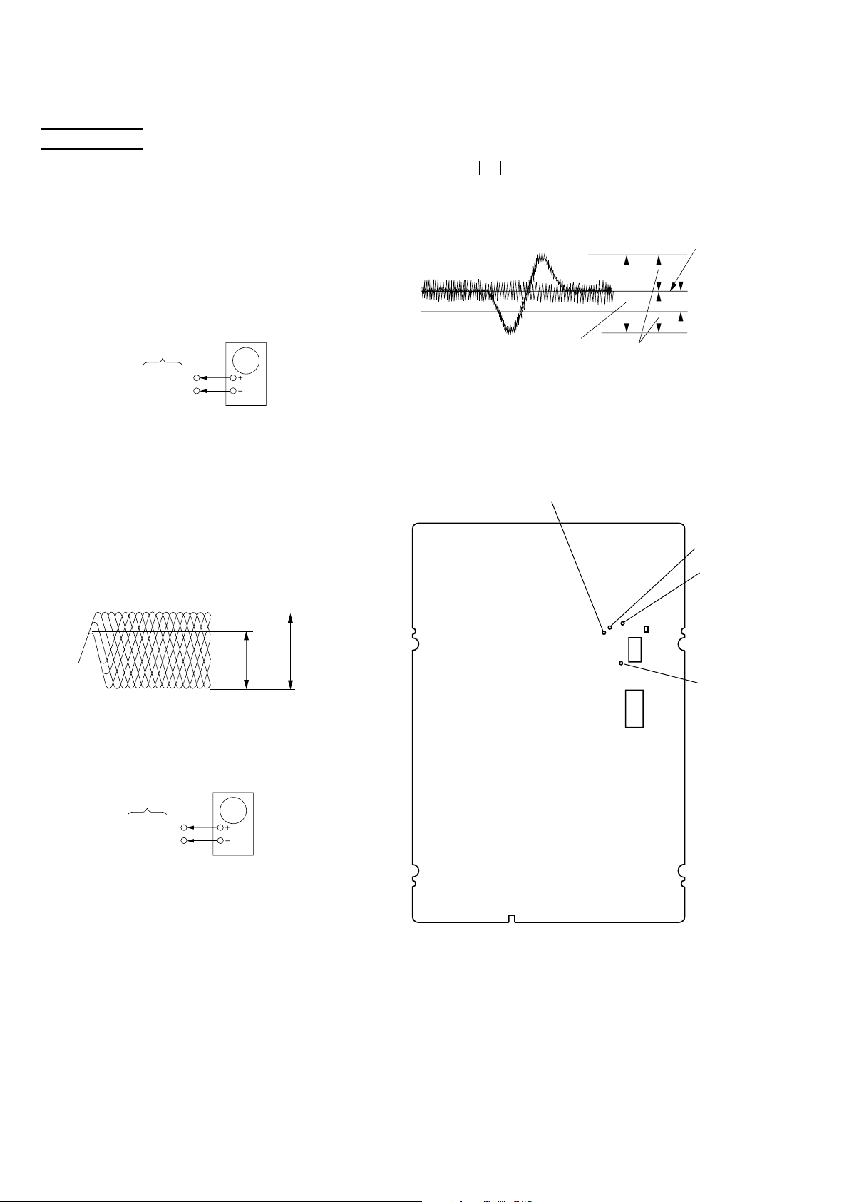
CD SECTION
Note :
1. CD Block is basically designed to operate without adjustment.
Therefore, check each item in order given.
2. Use YEDS-18 disc (3-702-101-01) unless otherwise indicated.
3. Use an oscilloscope with more than 10MΩ impedance.
4. Clean the object lens by an applicator with neutral detergent
when the signal level is low than specified value with the following checks.
RF Level Check
oscilloscope
BD board
TP(RFAC)
TP(VC)
Procedure :
1. Connect oscilloscope to TP (RFAC) and TP (VC).
2. Turned Power switch on.
3. Load a disc (YEDS-18) and playback.
4. Confirm that oscilloscope waveform is clear and check RF signal level is correct or not.
Procedure :
1. Connect oscilloscope to TP (RF-TE) and TP (VC).
2. Turned Power switch on.
3. Load a disc (YEDS-18) and playback the number five track.
4. Press the X button. (Becomes the 1 track jump mode.)
5. Confirm that the level B and A (DC voltage) on the oscilloscope waveform.
1 track jump waveform
0V
level=1.3±0.6Vp-p
Specified level: –– × 100=less than ±22%
A
B
B
symmetry
center of
waveform
A (DC voltage
Adjustment Location:
[BD BOARD] (Conductor Side)
TP (RFAC)
Note : Clear RF signal waveform means that the shape “ ◊ ” can be clearly
distinguished at the center of the waveform.
RF signal waveform
VOLT/DIV : 200mV
TIME/DIV : 500ns
3T
3T= 0.55
11T= 0.90
11T
±
0.07Vp-p
±
0.13Vp-p
E-F Balance (1 Track jump) Check
oscilloscop
BD board
TP(RF-TE)
TP(VC)
TP (RF-FE)
TP (RF-TE)
TP (VC)
IC101
TP
(RFDC)
IC401
20
CD-R SECTION
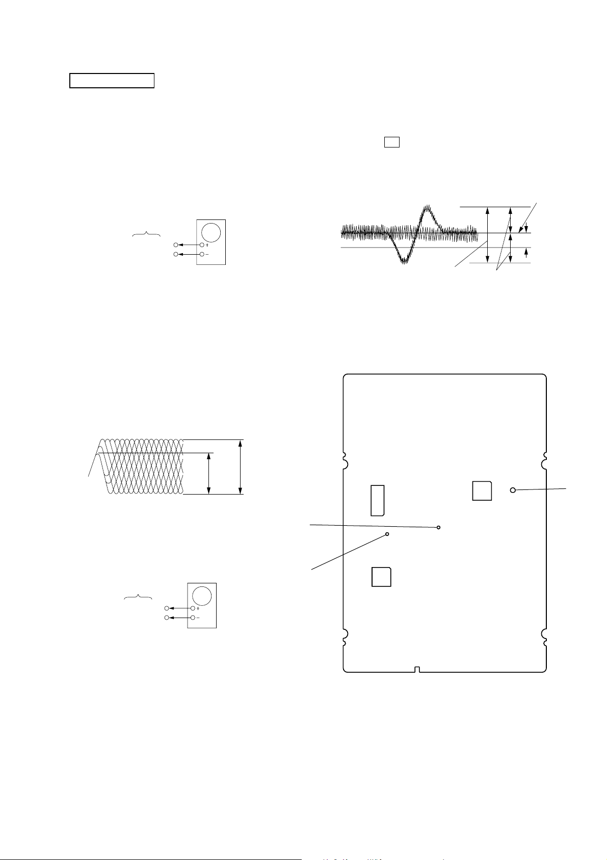
e
level=1.3±0.6Vp-p
symmetry
A (DC voltage)
center of
waveform
B
0V
1 track jump waveform
Specified level: –– × 100=less than ±22%
B
A
Note :
1. CD Block is basically designed to operate without adjustment.
Therefore, check each item in order given.
2. Use YEDS-18 disc (3-702-101-01) unless otherwise indicated.
3. Use an oscilloscope with more than 10MΩ impedance.
4. Clean the object lens by an applicator with neutral detergent
when the signal level is low than specified value with the following checks.
RF Level Check
oscilloscope
BD-R board
TP(RRF IN)
1
IC406
Procedure :
1. Connect oscilloscope to TP (RRFIN) and IC406 1 pin.
2. Turned Power switch on.
3. Load a disc (YEDS-18) and playback.
4. Confirm that oscilloscope waveform is clear and check RF signal level is correct or not.
pin
RCD-W1
Procedure :
1. Connect oscilloscope to TP (TE) and IC406 1 Pin.
2. Turned Power switch on.
3. Load a disc (YEDS-18) and playback the number five track.
4. Press the X button. (Becomes the 1 track jump mode.)
5. Confirm that the level B and A (DC voltage) on the oscilloscope waveform.
Adjustment Location:
[BD-R BOARD] (Conductor Side)
Note : Clear RF signal waveform means that the shape “ ◊ ” can be clearly
distinguished at the center of the waveform.
RF signal waveform
VOLT/DIV : 200mV
TIME/DIV : 500ns
3T
3T= 0.55
11T= 0.90
11T
±
0.07Vp-p
±
0.13Vp-p
TP
(FE)
E-F Balance (1 Track jump) Check
TP
(TE)
BD-R board
TP(TE)
1
IC406
oscilloscop
pin
IC203
TP
(RRF IN)
IC401
IC701
( See next page for the component side location. )
21

RCD-W1
[BD-R BOARD] (Conponent Side)
IC406
1 pin
IC406
8
1
4
5
IC401
IC413
22
THIS NOTE IS COMMON FOR PRINTED WIRING
BOARDS AND SCHEMATIC DIAGRAMS.
(In addition to this, the necessary note is printed
in each block.)
For schematic diagrams.
Note:
• All capacitors are in µF unless otherwise noted. pF: µµF
50 WV or less are not indicated except for electrolytics
and tantalums.
• All resistors are in Ω and 1/
specified.
• % : indicates tolerance.
¢
•
• C : panel designation.
Note:
The components identified by mark ! or dotted
line with mark ! are critical for safety.
Replace only with part
number specified.
• A : B+ Line.
• B : B– Line.
• H : adjustment for repair.
• AC voltage readings in the bias oscillator with a level
• Voltages and waveforms are dc with respect to ground
• Voltages are taken with a VOM (Input impedance 10 MΩ).
• Waveforms are taken with a oscilloscope.
• Circled numbers refer to waveforms.
: internal component.
meter.
under no-signal conditions.
no mark : STOP
( ) : PLAY
< > : REC (CD-R only)
Voltage variations may be noted due to normal production tolerances.
Voltage variations may be noted due to normal production tolerances.
4
W or less unless otherwise
Note:
Les composants identifiés par
une marque ! sont critiques
pour la sécurité.
Ne les remplacer que par une
piéce portant le numéro
spécifié.
SECTION 5
DIAGRAMS
• Signal path.
J : CD play
c : digital out
I : CD REC
• Abbreviation
CND : Canadian model.
MX : Mexican model.
For printed wiring boards.
Note:
• : Pattern from the side which enables seeing.
(The other layers' patterns are not indicated.)
Caution:
Pattern face side: Parts on the pattern face side seen from the
(Side B) pattern face are indicated.
Parts face side: Parts on the parts face side seen from the
(Side A) parts face are indicated.
• Indication of transistor
C
Q
• Abbreviation
CND : Canadian model.
MX : Mexican model.
These are omitted
EB
C
EB
These are omitted
RCD-W1
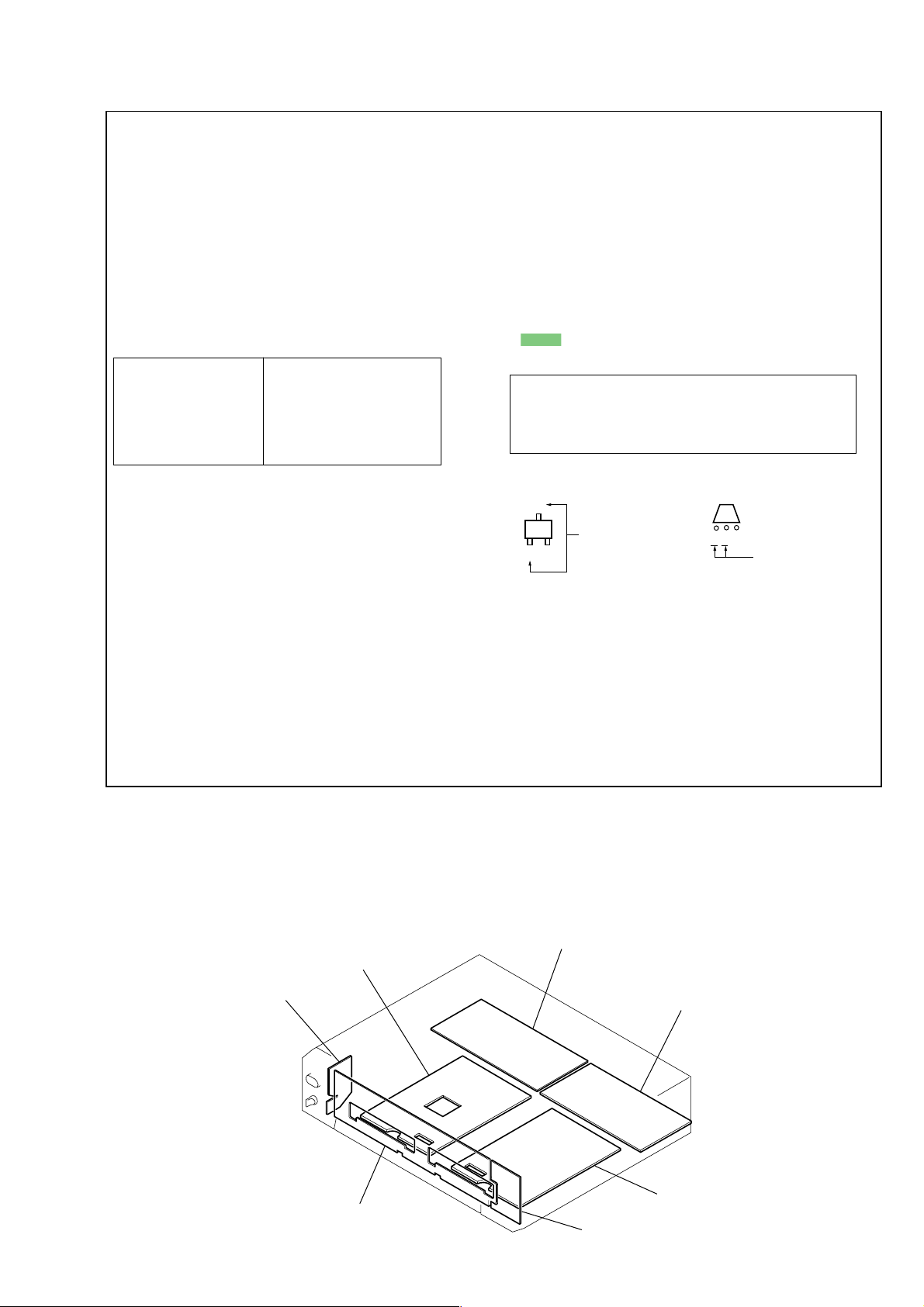
5-1. CIRCUIT BOARDS LOCATION
BD board
HP board
FL board
POWER board
VOL board
board
AUDIO
BD-R board
23
RCD-W1
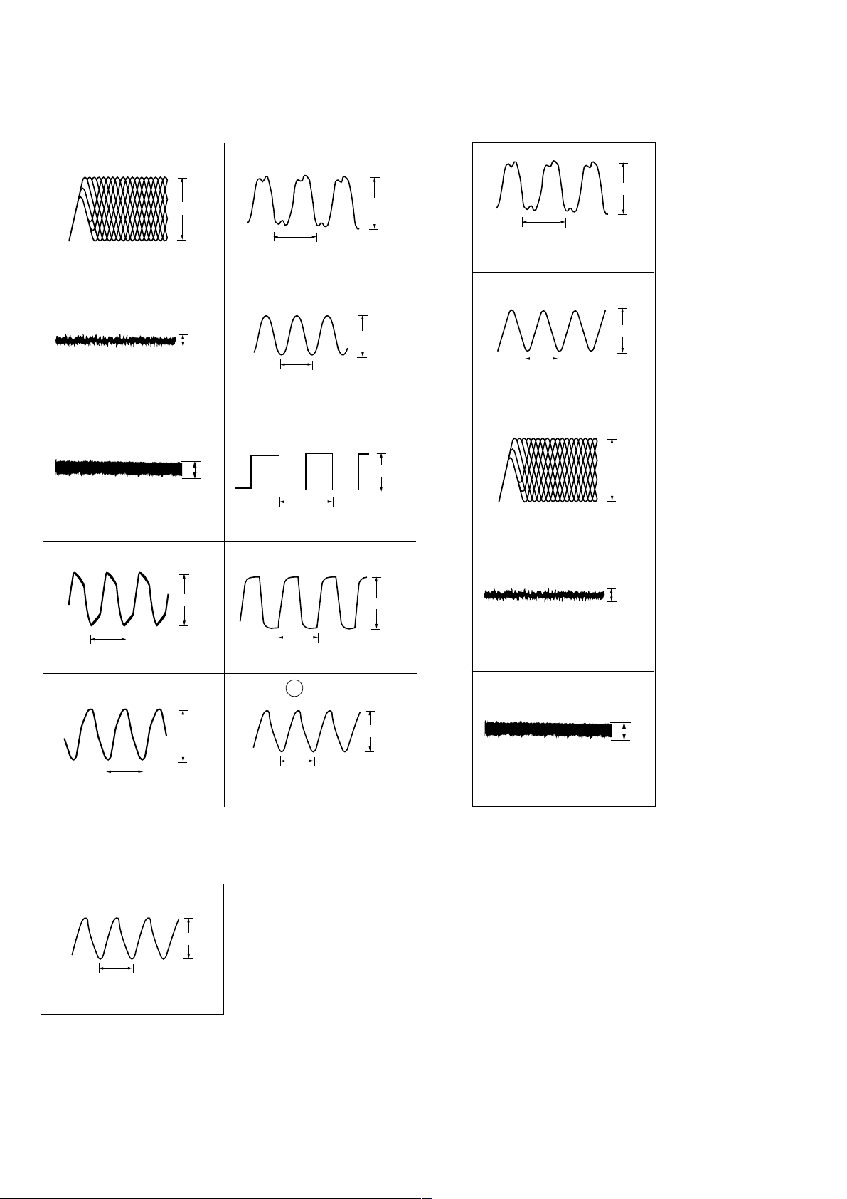
1.7Vp-p
50nsec
(20MHz)
WAVEFORMS
– CDR SECTION –
IC401 ig (RRFIN)
1
PLAY MODE
0.2V/dic
500nsec/div
IC401 th (FE)
2
PLAY MODE
0.8Vp-p
IC301 uf (CDP33M)
6
29.5nsec
(33.86880MHz)
IC701 yh (EXTAL)
7
4.8Vp-p
– CD SECTION –
IC201 id (XTLO)
1
29.5nsec
(33.86880MHz)
2V/div
20nsec/div
IC501 yh (EXTAL)
2
5.0Vp-p
0.2V/div
500nsec/div
IC401 tj (TE)
3
PLAY MODE
0.2V/div
500µsec/div
IC310 4
4
2.9nsec
(33.86880MHz)
IC301 yg (CLK_IN)
5
29.5nsec
(33.86880MHz)
0.1Vp-p
0.3Vp-p
4.0Vp-p
2.2Vp-p
29.5nsec
(33.86880MHz)
IC306 qs (ILRCK)
8
22.5µsec
IC306 qd (ISCLK)
9
0.36µsec
IC201 149 (XIN)
0
29.5nsec
(33.86880MHz)
1.7Vp-p
4.8Vp-p
1Vp-p
5.0Vp-p
IC101 qg (RFAC)
3
PLAY MODE
500nsec/div
IC101 qh (FF)
4
PLAY MODE
0.1V/div
5msec/div
IC101 qk (TE)
5
PLAY MODE
0.2V/dic
1V/div
5msec/div
0.8Vp-p
0.2Vp-p
1.0Vp-p
– PANEL SECTION –
IC801 4 (X2)
1
0.2µsec
(5MHz)
24
4.8Vp-p
 Loading...