Sony RCDW-1 Service manual
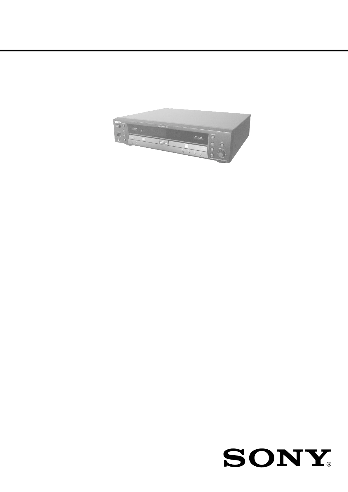
RCD-W1
SERVICE MANUAL
Ver 1.1 2001.04
SPECIFICATIONS
DECK A (the CD player section)
System Compact disc and digital
Frequency response 20 Hz – 20,000 kHz (±0.5
Signal-to-noise ratio More than 100 dB
Dynamic range More than 93 dB
DECK B (the CD-R and CD-RW
recording section)
System Compact disc digital audio
Playable discs CD, CD-R, CD-RW
Recordable discs CD-R, CD-RW (for music
Frequency response 20 to 20,000 Hz ±0.5 dB
Signal-to-noise ratio Over 96 dB during
Dynamic range More than 93 dB during
Inputs
ANALOG IN
(Phono jacks) impedance 47 kilohms
DIGITAL OPTICAL IN
(Square optical connector jack)
audio system
dB)
system
use)
playback
playback
Rated input 330 mVrms
Minimum input
125 mVrms
Optical wavelength
660 nm
Canadian Model
Outputs
ANALOG OUT
(Phono jacks) impedance 47 kilohms
OPTICAL DIGITAL OUT
(Square optical connector jack)
General
Power requirements
U.S.A. and Canada 120 V AC, 60 Hz
Power consumption 28 W
Dimensions (approx.) (w/h/d) incl. projecting parts
Mass (approx.) 4.6 kg
Supplied accessories
Design and specifications are subject to change
without notice.
Rated output 2 Vrms
Load impedance over
10 kilohms
Wavelength 660 nm
Output level -18 dBm
and control
430 × 108 × 368 mm
• Audio connecting cord (2)
• Remote commander (remote) (1)
• Size AA (R6) batteries (2).
US Model
E Model
9-929-582-12
2001D0900-1
© 2001. 4
COMPACT DISC RECORDER
Sony Corporation
Home Audio Company
Shinagawa Tec Service Manual Production Group
1
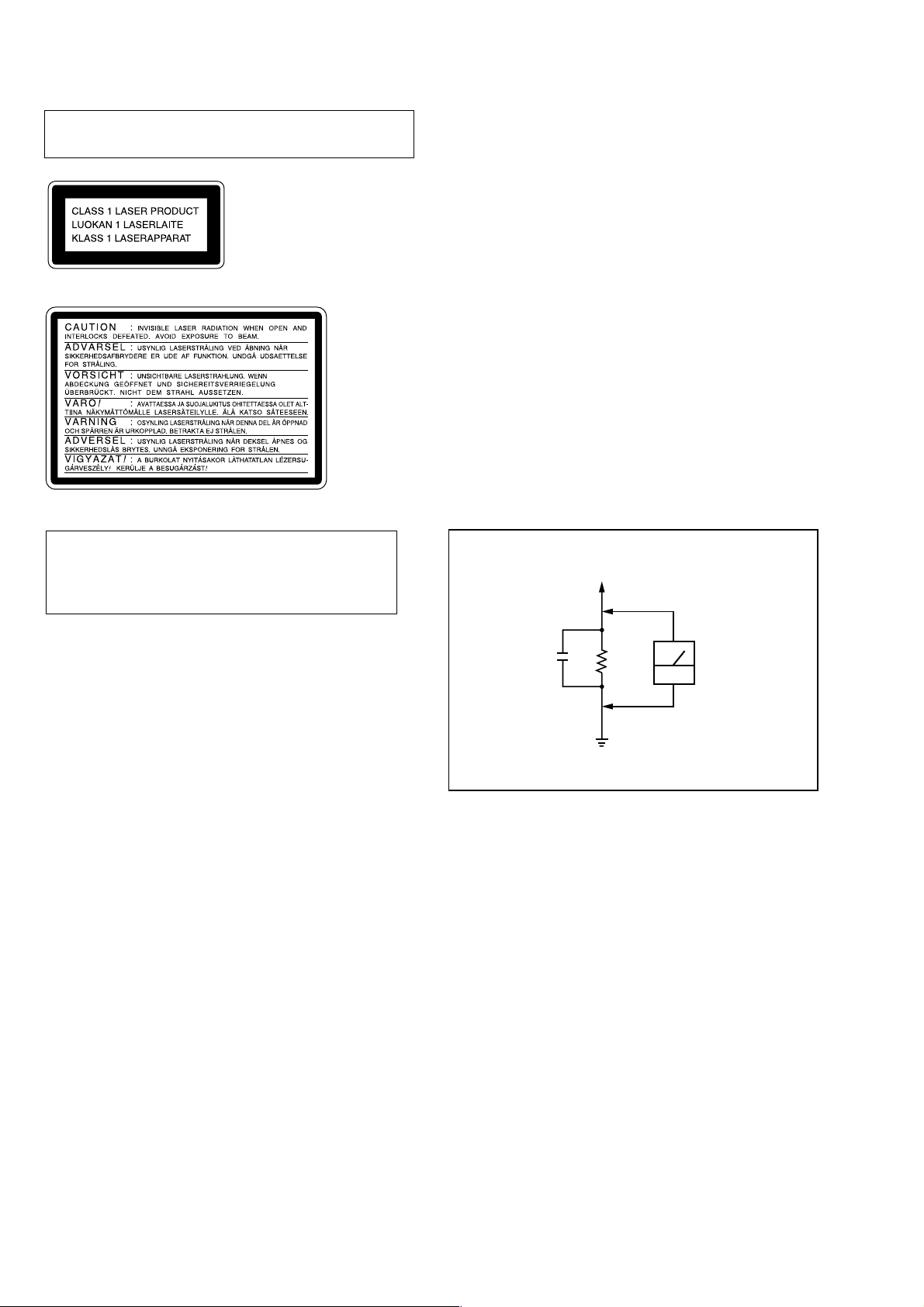
Laser component in this product is capable of emitting radiation
exceeding the limit for Class 1.
This appliance is classified as
a CLASS 1 LASER product.
The CLASS 1 LASER PRODUCT MARKING is located on
the rear exterior.
This caution
label is located
inside the unit.
SAFETY CHECK-OUT
After correcting the original service problem, perform the following safety checks before releasing the set to the customer:
Check the antenna terminals, metal trim, “metallized” knobs, screws,
and all other exposed metal parts for A C leakage. Check leakage as
described below.
LEAKAGE
The AC leakage from any exposed metal part to earth Ground and
from all exposed metal parts to any exposed metal part having a
return to chassis, must not exceed 0.5 mA (500 microampers). Leakage current can be measured by any one of three methods.
1. A commercial leakage tester, such as the Simpson 229 or RCA
WT-540A. Follow the manufacturers’ instructions to use these
instruments.
2. A battery-operated AC milliammeter. The Data Precision 245
digital multimeter is suitable for this job.
3. Measuring the voltage drop across a resistor by means of a V OM
or battery-operated AC voltmeter . The “limit” indication is 0.75
V, so analog meters must have an accurate low-voltage scale.
The Simpson 250 and Sanwa SH-63Trd are examples of a passive VOM that is suitable. Nearly all battery operated digital
multimeters that have a 2V AC range are suitable. (See Fig. A)
CAUTION
Use of controls or adjustments or performance of procedures
other than those specified herein may result in hazardous radiation exposure.
Notes on chip component replacement
• Never reuse a disconnected chip component.
• Notice that the minus side of a tantalum capacitor may be
damaged by heat.
Flexible Circuit Board Repairing
• Keep the temperature of soldering iron around 270˚C
during repairing.
• Do not touch the soldering iron on the same conductor of the
circuit board (within 3 times).
• Be careful not to apply force on the conductor when soldering
or unsoldering.
TABLE OF CONTENTS
1. GENERAL.................................................................... 3
2. DIAGRAMS
2-1. Circuit Board Location ....................................................... 4
2-2. Block Diagrams .................................................................. 5
2-3. Schematic Diagram – CDP Section –................................. 8
2-4. Schematic Diagram – MAIN Section –.............................. 9
2-5. Schematic Diagram – PANEL Section – ..........................10
2-6. Schematic Diagram – CD-R (1/2) Section – .................... 11
2-7. Schematic Diagram – CD-R (2/2) Section – .................... 12
2-8. Schematic Diagram – Power Section – ............................ 13
2-9. IC Pin Functions ............................................................... 14
To Exposed Metal
Parts on Set
0.15µF
1.5kΩ
Earth Ground
AC
voltmeter
(0.75V)
Fig. A. Using an AC voltmeter to check AC leakage.
3. EXPLODED VIEWS
3-1. Front Panel Section .......................................................... 19
3-2. Chassis Section................................................................. 20
3-3. CD Play Section ............................................................... 21
3-4. CD Record Section ........................................................... 22
4. ELECTRICAL PARTS LIST................................. 23
SAFETY-RELATED COMPONENT WARNING !!
COMPONENTS IDENTIFIED BY MARK 0 OR DOTTED LINE
WITH MARK 0 ON THE SCHEMATIC DIAGRAMS AND IN
THE PARTS LIST ARE CRITICAL TO SAFE OPERATION.
REPLACE THESE COMPONENTS WITH SONY PARTS
WHOSE PART NUMBERS APPEAR AS SHOWN IN THIS
MANUAL OR IN SUPPLEMENTS PUBLISHED BY SONY.
2
ATTENTION AU COMPOSANT AYANT RAPPORT
À LA SÉCURITÉ!
LES COMPOSANTS IDENTIFÉS P AR UNE MARQUE 0 SUR LES
DIAGRAMMES SCHÉMA TIQUES ET LA LISTE DES PIÈCES SONT
CRITIQUES POUR LA SÉCURITÉ DE FONCTIONNEMENT. NE
REMPLACER CES COMPOSANTS QUE PAR DES PIÈSES SONY
DONT LES NUMÉROS SONT DONNÉS DANS CE MANUEL OU
DANS LES SUPPÉMENTS PUBLIÉS PAR SONY.
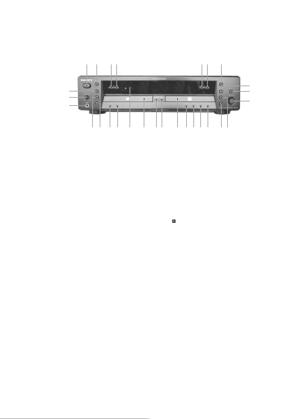
FRONT PANEL
21 34 56 7
q
q
q
q
q
q
w
w;qlq
wdw
w
w
q
wk
wj
wh
SECTION 1
GENERAL
8
9
0
f
g
LOCATION OF PARTS AND CONTROLS
1 Power button
2 OPEN/CLOSE A button (DECK A)
3 . AMS button (DECK A)
4 > AMS button (DECK A)
5 . AMS button (DECK B)
6 > AMS button (DECK B)
7 OPEN/CLOSE A button (DECK B)
8 H button (DECK B)
9 z REC button
q; REC LEVEL knob (DECK B)
qa X button (DECK B)
qs x button (DECK B)
qd INPUT button (DECK B)
qf TIME button (DECK B)
a
s
k
j
qg ERASE button (DECK B)
qh FINALIZE button (DECK B)
qj DISC tray (DECK B)
qk CD SYNCHRO HIGH button
ql CD SYNCHRO NORMAL button
w; DISC tray (DECK A)
remote sensor
wa
ws TIME button (DECK A)
wd RELAY button (DECK A)
wf x button (DECK A)
wg X button (DECK A)
wh PHONE jack
wj PHONE LEVEL knob
wk H button (DECK A)
g
h
d
f
s
a
3
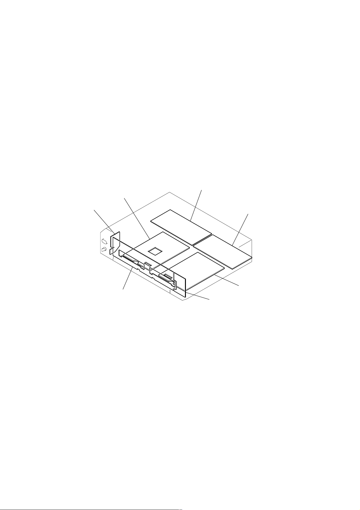
2-1. CIRCUIT BOARDS LOCATION
SECTION 2
DIAGRAMS
POWER board
CDP board
HP board
MAIN board
CD-R board
FL board
VOL board
4
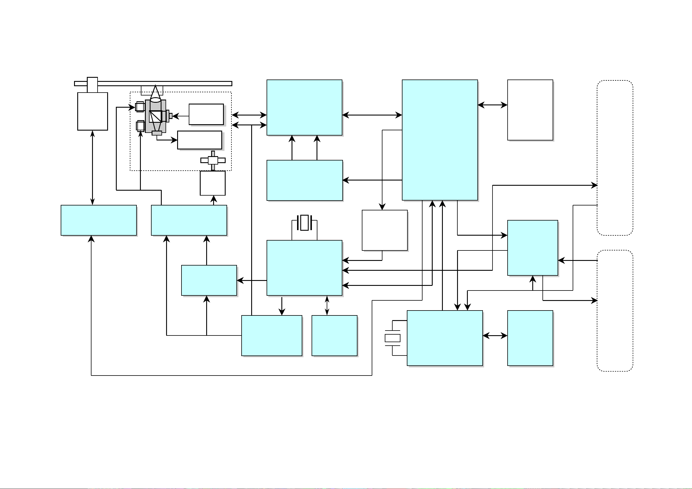
2-2. BLOCK DIAGRAMS
– CD RECORD SECTION –
Spindle
motor
disc
Pick-up
(KRS-220c
:Sony)
LD
Driver
I / V AMP
motor
Sled
IC401
CXA2551AR
RF AMP
Wobble
ALPC
S/H 17.43MHz
IC601
CPLD
Laser Control
S/H Signal Gen
RF/Servo Signal
Timing
Signal
IC201
OTI9790
DSP + SERVO
Decoder
Encoder
ATIP Demod
Write Strategy
I/F
RCD-W1
2MB
DRAM
CDP
I/F
IC510
BA6664FM-E2
Motor drive
IC501
BA5983FM
F.T.S.T drive
BA5925
Sled Speed
IC502
IC409
M62352
12CH 8 bit DAC
IC701
H8/3062
System
Controller
X701
20MHz
IC702
AT93C86
1KB EEPROM
OPC/
ROPC
Circuit
X301
33.86MHz
IC301
ASIC
VC00S01
D-out
Serial data MCLK
IC306
SRC
CS8420
IC302
256K
SRAM
Serial /AES3
output
I/O
5
5
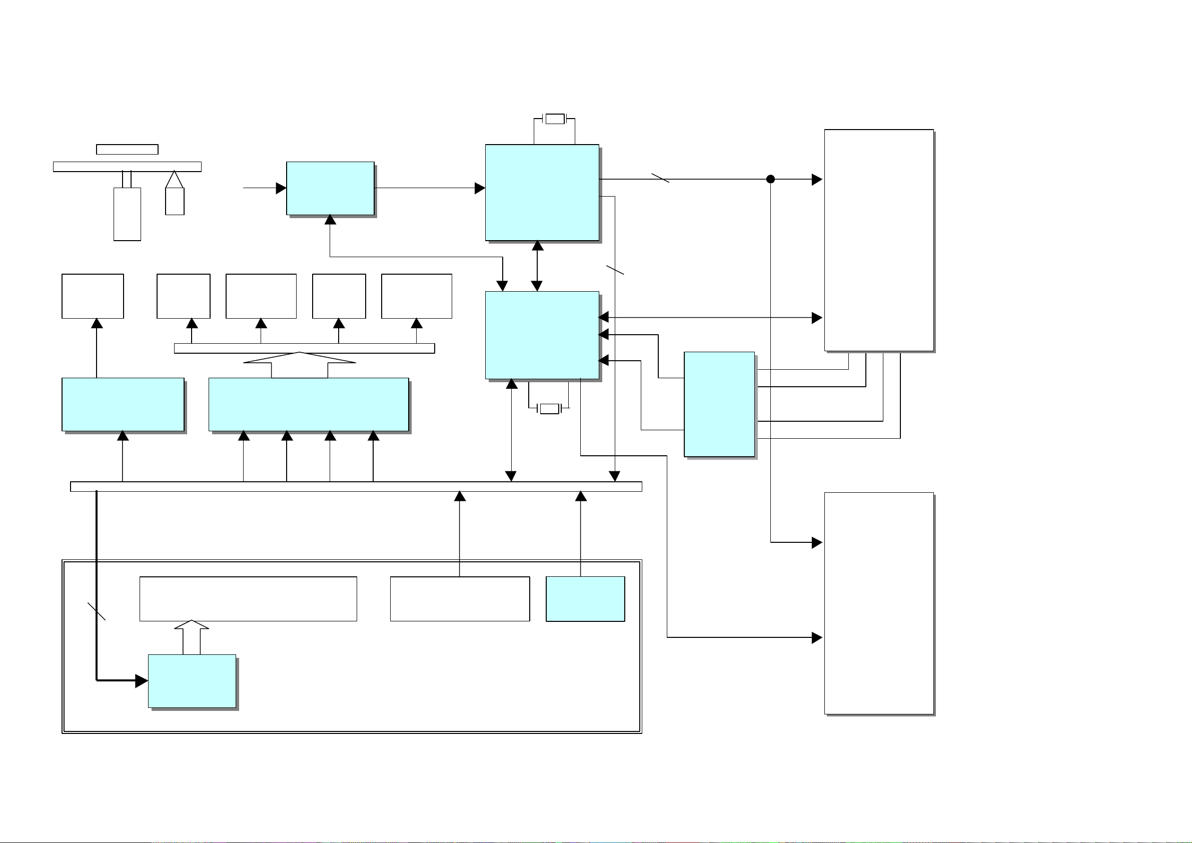
RCD-W1
– CD PLAY SECTION –
DISC
MOTOR
UNIT
SPINDLE
MOTOR
MOTOR DRIVE
CS
BLK
CLK
TXD
IC401
LB1195H
SPINDLE
DRIVE
SIGNAL
FOCUS
COIL
LASER
PICK-UP
IC101
CXA2581N
RF AMP
TRACKING
COIL
IC301
M56788FP
MOTOR DRIVER
F.DRV T.DRV SLED LOADING
SLED
MOTOR
LOADING
MOTOR
33.86MHz
IC201
CXD3011-1R
DSP + SSP
IC501
H8/3062
SYSTEM
CONTROLLER
SLED
LOADING
FLD_CS
FLD_BLK
FLD_CLK
TXD
AD-DATA RMC-IN
20MHz
F.DRV
T.DRV
SPINDLE DRV
REC_CLK
REC_TXD
IC602
BU4053
S/W
LRCK
DATA
BCLK
MCLK
C
D
R
W
ASIC CLK
RW-CLK
ASIC DIN
RW_TXD
LRCK
DATA
BCLK
MCLK
D_OUT
IC801
UPD780232GC
DRIVER
DIGITRON
KEY SCAN
RMC801
REMOTE
SENSOR
6
6
EQ_LEVEL
EMPH
MUTE
P_DOWN
I/O
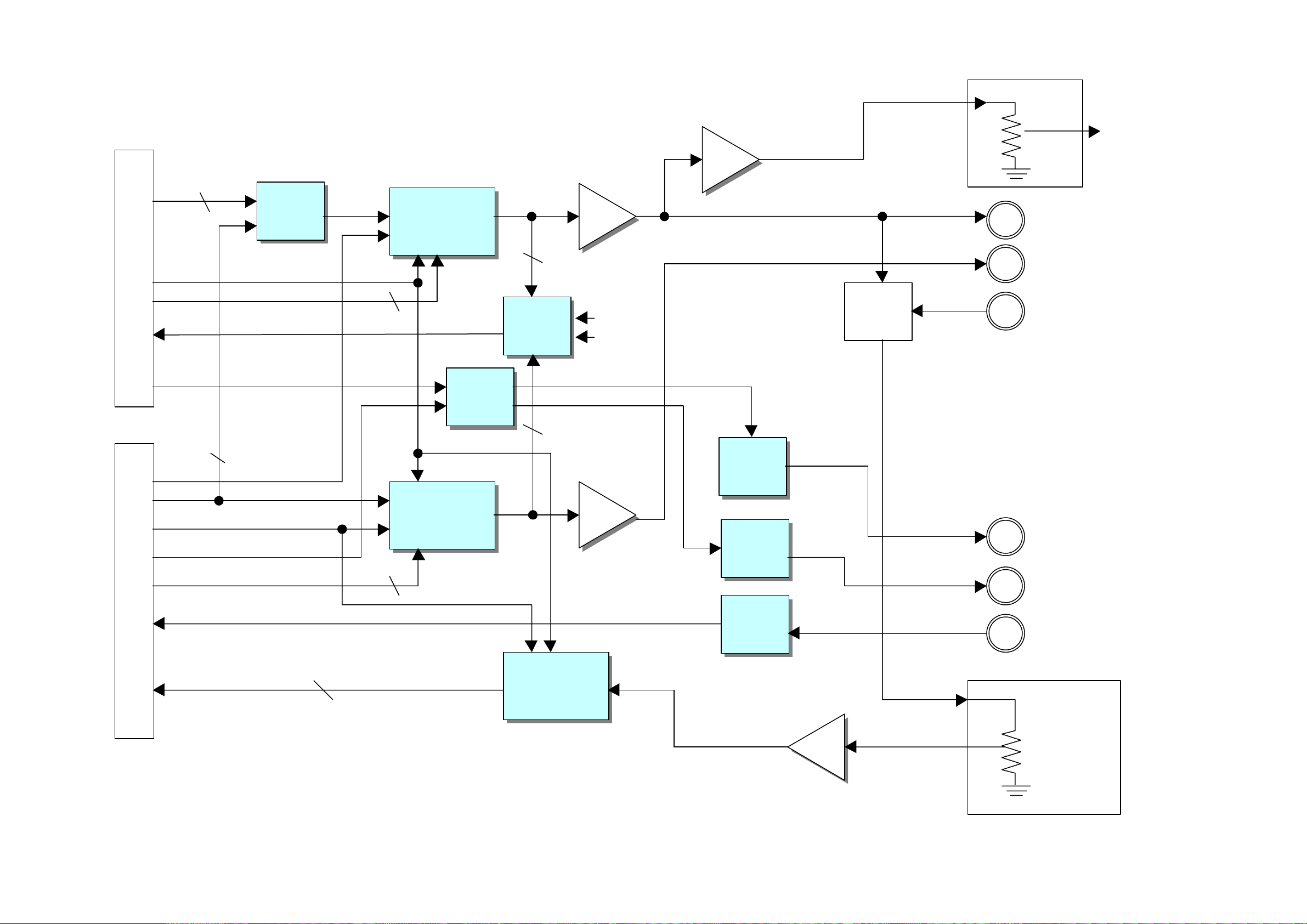
– I/O SECTION –
C
LRCK
DATA
BCLK
IC108, 109,
110, 111
BU4053 S/W
IC401
AK4393
(DAC)
RCD-W1
H/P OUT
ANALOG P OUTPUT
POWER
D
P
C
D
DOWN
CDP-DOUT
LRCK
DATA
BCLK
MCK(P)
MCK(R)
CDR-DOUT
MUTE
DEMPH
IC401
AK4393
(DAC)
MUTE
DEMPH
IC302
TC4W53FU
S/W
IC108, 109,
110, 111
BU4053 S/W
L/R
CDP/CDR
EQ LEVEL
RELAY
IC106
74HC04
BUFFER
IC106
74HC04
BUFFER
ANALOG R OUTPUT
ANALOG INPUT
OPTICAL P OUT
OPTICAL R OUT
R
W
BCK
DATA
LRCK
IC112
AK5351
(ADC)
7
74HC04
BUFFER
7
IC106
REC
VOL.
OPTICAL IN
F
R
O
N
T
RCD-W1
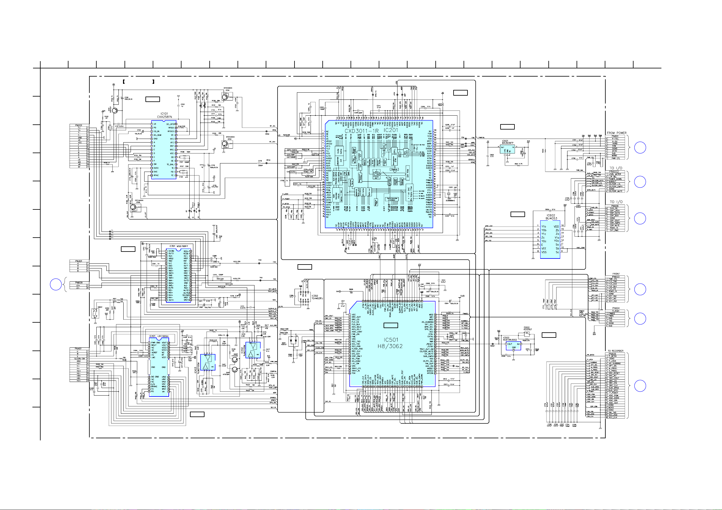
2-3. SCHEMATIC DIAGRAM – CDP SECTION – • See page 14 for IC Pin Functions.
1
A
2
3
4
CDP BOARD
IC101
5
RF AMP
6
7
98
10
11
12
13
14
15
IC201
DSP + SSP
16
17
18
19
20
21
22
B
TO PICK-UP
IC601
4V REGULATOR IC
C
E
TO POWER BOARD
D
(Page 13)
D
E
IC602
ANALOG SW
F
TO MAIN BOARD
(Page 9)
G
TO MAIN BOARD
(Page 9)
G
H
I
J
K
L
M
TO LOADING MOTOR
N
TO CD-R BOARD (1/2)
(Page 11)
TO SPINDLE MOTOR
TO SLED MOTOR
IC301
MOTOR
DRIVE IC
IC401
MOTOR
DRIVE IC
IC302
ANALOG SW
IC501
CD MICON
IC502
RESET IC
H
TO FL BOARD
(Page 10)
I
TO CD-R BOARD(1/2)
(Page 11)
A
TO CD-R BOARD
(Page 11)
8
8
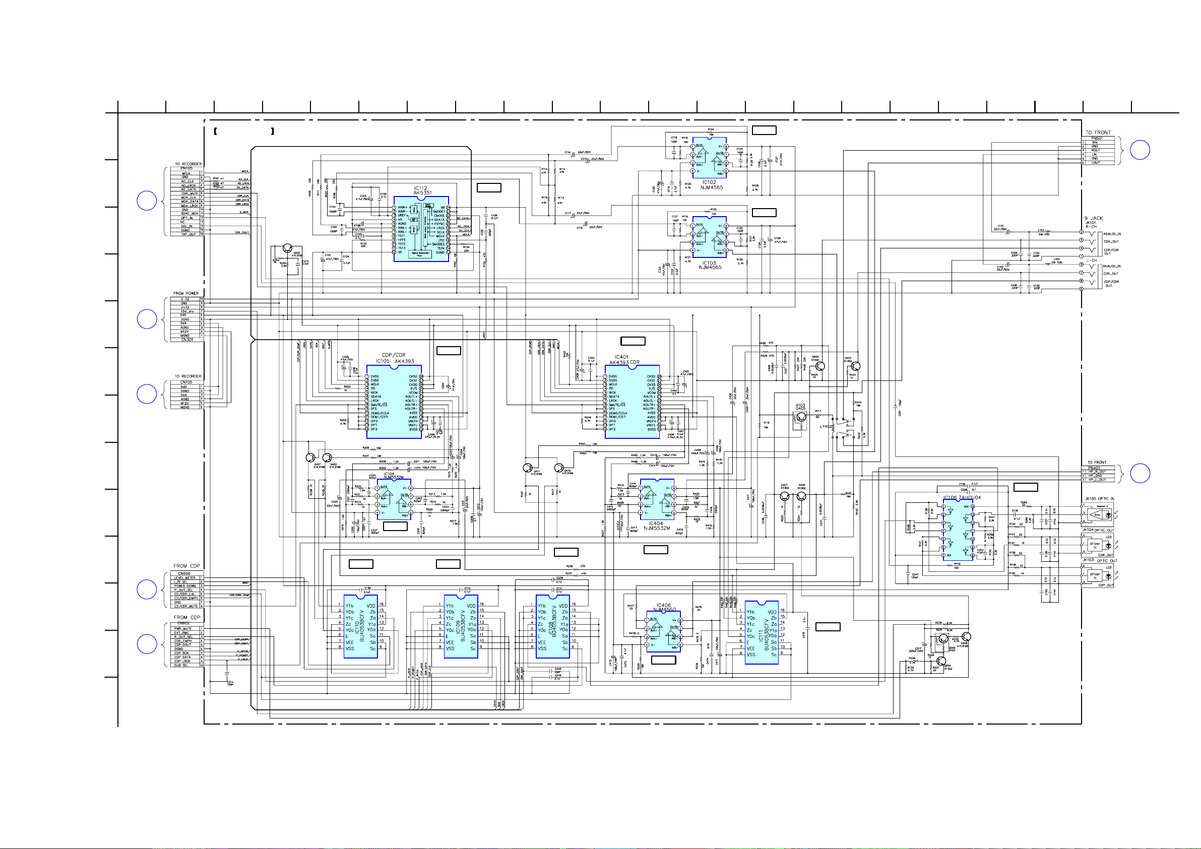
2-4. SCHEMATIC DIAGRAM – MAIN SECTION –
RCD-W1
1
A
2
3
4
MAIN BOARD
5
6
7
98
10
11
12
13
14
IC102
LINE AMP
15
16
17
18
19
20
2221
J
TO VOL BOARD
B
IC112
ADC
(Page 10)
B
TO CD-R
BOARD (1/2)
C
(Page 11)
D
E
F
TO POWER
BOARD
(Page 13)
IC105
DAC
IC401
DAC
F
IC103
LINE AMP
M
TO CD-R
BOARD (1/2)
G
(Page 11)
H
K
IC106
BUFFER
I
IC104
MIX AMP
J
TO CDP
BOARD
(Page 8)
IC110
SELECTOR
IC109
SELECTOR
IC108
SELECTOR
IC404
MIX AMP
TO HP BOARD
(Page 10)
D
K
IC111
SELECTOR
L
M
G
TO CDP
BOARD
(Page 8)
IC406
HEADPHONE AMP
9
9
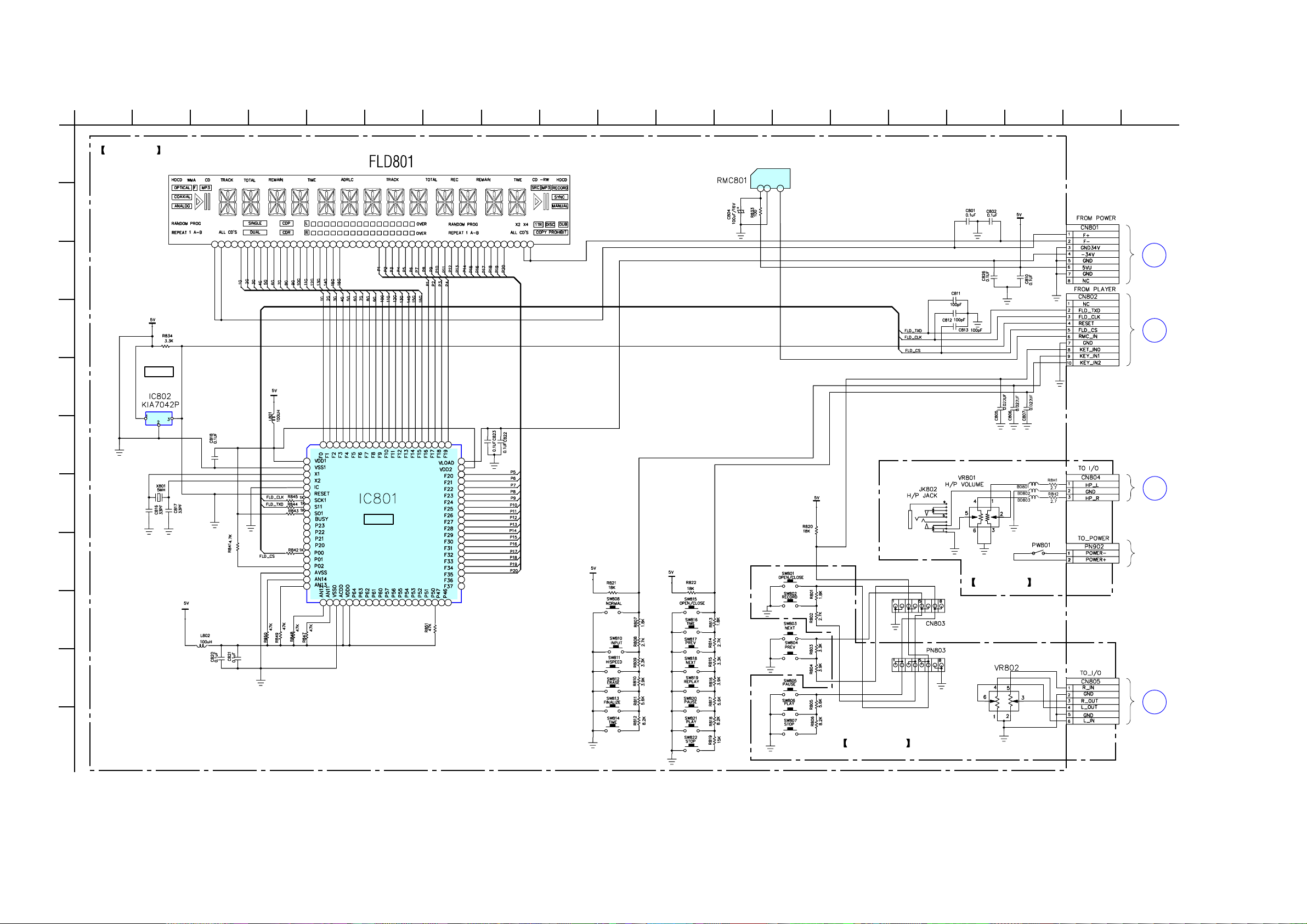
RCD-W1
2-5. SCHEMATIC DIAGRAM – PANEL SECTION – • See page 15 for IC Pin Functions.
1
A
FL BOARD
2
3
4
5
6
7
98
10
11
12
REMOTE SENSOR
13
14
15
1716
18
19
B
L
C
D
IC802
E
RESET IC
TO POWER BOARD
(Page 13)
H
TO CDP BOARD
(Page 8)
F
G
H
80 79 78 77 76 75 74 73 72 71 70 69 68 67 66 65 64 63 62 61
1
2
3
4
5
6
7
8
9
10
11
12
13
14
15
16
17
18
19
20
21 22 23 24 25 26 27 28 29 30 31 32 33 34 35 36 37 38 39 40
UPD780232GC-LG1
IC801
FL DRIVER
60
59
58
57
56
55
54
53
52
51
50
49
48
47
46
45
44
43
42
41
HP BOARD
K
TO MAIN BOARD
(Page 9)
TO POWER BOARD
(Page 13)
I
J
J
TO MAIN BOARD
K
VOL BOARD
(Page 9)
10
10
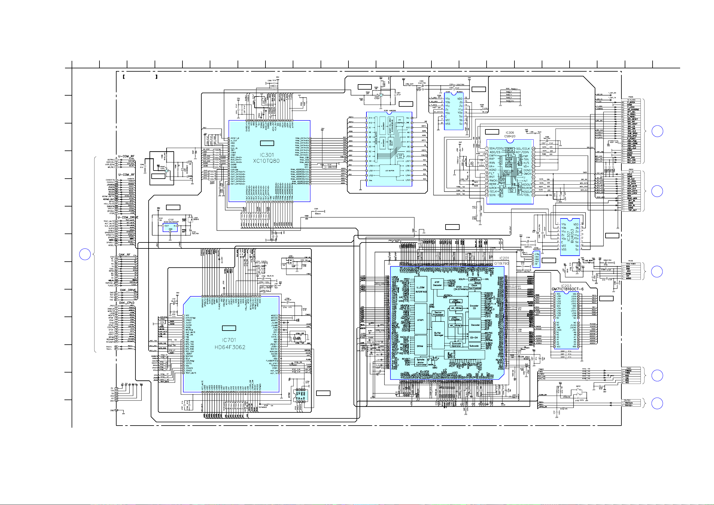
2-6. SCHEMATIC DIAGRAM – CD-R (1/2) SECTION –
RCD-W1
A
B
C
D
E
F
G
H
1
C
TO CD-R
BOARD (1/2)
(Page 12)
2
CD-R BOARD (1/2)
3
4
5
6
7
IC301
SERIAL PARAREL
CONVERT IC
98
3.3K
10
11
IC303
12
IC302
256K SRAM
13
14
15
IC304
SELECTOR
IC306
SRC
16
17
18
19
20
21 22
A
TO CDP BOARD
(Page 8)
IC310
B
TO MAIN BOARD
(Page 9)
IC101
RESET IC
IC201
DSP/SERVO
100u
IC307
SELECTOR
0.33u
IC102
+3V REGULATOR
M
TO MAIN BOARD
(Page 9)
IC203
I
J
IC701
CDR DEVICE INPUT
CONTROL MICON
D RAM
K
I
L
IC702
CAT93C86S
1KB EEPROM
TO CDP BOARD
(Page 8)
N
M
TO CDP BOARD
(Page 8)
11
11
 Loading...