

Page 1

SOLID-STATE MEMORY CAMCORDER
PMW-EX3
SERVICE MANUAL
1st Edition
Page 2
! WARNING
This manual is intended for qualified service personnel only.
To reduce the risk of electric shock, fire or injury, do not perform any servicing other than that
contained in the operating instructions unless you are qualified to do so. Refer all servicing to
qualified service personnel.
! WARNUNG
Die Anleitung ist nur für qualifiziertes Fachpersonal bestimmt.
Alle Wartungsarbeiten dürfen nur von qualifiziertem Fachpersonal ausgeführt werden. Um die
Gefahr eines elektrischen Schlages, Feuergefahr und Verletzungen zu vermeiden, sind bei
Wartungsarbeiten strikt die Angaben in der Anleitung zu befolgen. Andere als die angegeben
Wartungsarbeiten dürfen nur von Personen ausgeführt werden, die eine spezielle Befähigung
dazu besitzen.
! AVERTISSEMENT
Ce manual est destiné uniquement aux personnes compétentes en charge de l’entretien. Afin
de réduire les risques de décharge électrique, d’incendie ou de blessure n’effectuer que les
réparations indiquées dans le mode d’emploi à moins d’être qualifié pour en effectuer d’autres.
Pour toute réparation faire appel à une personne compétente uniquement.
PMW-EX3
Page 3
CAUTION
ADVARSEL!
Lithiumbatteri-Eksplosionsfare ved fejlagtig
håndtering.
Udskiftning må kun ske med batteri
af samme fabrikat og type.
Levér det brugte batteri tilbage til leverandøren.
Danger of explosion if battery is incorrectly replaced.
Replace only with the same or equivalent type
recommended by the manufacturer.
Dispose of used batteries according to the
manufacturer’s instructions.
Vorsicht!
Explosionsgefahr bei unsachgemäßem Austausch
der Batterie.
Ersatz nur durch denselben oder einen vom
Hersteller empfohlenen ähnlichen Typ. Entsorgung
gebrauchter Batterien nach Angaben des
Herstellers.
ATTENTION
Il y a danger d’explosion s’il y a remplacement
incorrect de la batterie.
Remplacer uniquement avec une batterie du même
type ou d’un type équivalent recommandé par le
constructeur.
Mettre au rebut les batteries usagées conformément
aux instructions du fabricant.
ADVARSEL
Lithiumbatteri - Eksplosjonsfare.
Ved utskifting benyttes kun batteri som
anbefalt av apparatfabrikanten.
Brukt batteri returneres
apparatleverandøren.
VARNING
Explosionsfara vid felaktigt batteribyte.
Använd samma batterityp eller en likvärdig typ
som rekommenderas av apparattillverkaren.
Kassera använt batteri enligt gällande
föreskrifter.
VAROITUS
Paristo voi räjähtää jos se on virheellisesti
asennettu.
Vaihda paristo ainoastaan laitevalmistajan
suosittelemaan tyyppiin.
Hävitä käytetty paristo valmistajan ohjeiden
mukaisesti.
PMW-EX3
1 (P)
Page 4

Page 5

Table of Contents
Manual Structure
Purpose of this manual ................................................................. 4
Related manuals ........................................................................... 4
1. Service Overview
1-1. External Connectors ........................................................ 1-1
1-1-1. Signal Inputs and Outputs ..................................... 1-1
1-2. Location of the Printed Wiring Boards ........................... 1-4
1-3. Circuit Description .......................................................... 1-5
1-4. Service Tools/Measuring Equipment List .................... 1-11
1-4-1. Service Tools ....................................................... 1-11
1-4-2. Measuring Equipment ......................................... 1-11
1-5. Firmware Upgrade ........................................................ 1-12
1-6. Recommended Replacement Parts ............................... 1-13
1-7. Note on Service ............................................................. 1-14
1-7-1. Requirements on Replacement of
Boards or Parts .................................................... 1-14
1-7-2. Note on Replacement of Parts on the Board ....... 1-14
1-7-3. Description of Number Seal on the Prism ........... 1-14
1-7-4. Memory Backup Battery ..................................... 1-14
1-7-5. Unleaded Solder .................................................. 1-14
1-8. Connector Location Diagram on Board ........................ 1-15
1-9. Replacing the Flexible Card Wires ...............................1-16
1-10. Replacing the Coaxial Cable with Connector
(Fine Pitch Coaxial Cable) ............................................ 1-16
1-11. List of Error Numbers on the LCD Display .................1-18
1-12. Servicing software “ServiceNavi-EX” ......................... 1-18
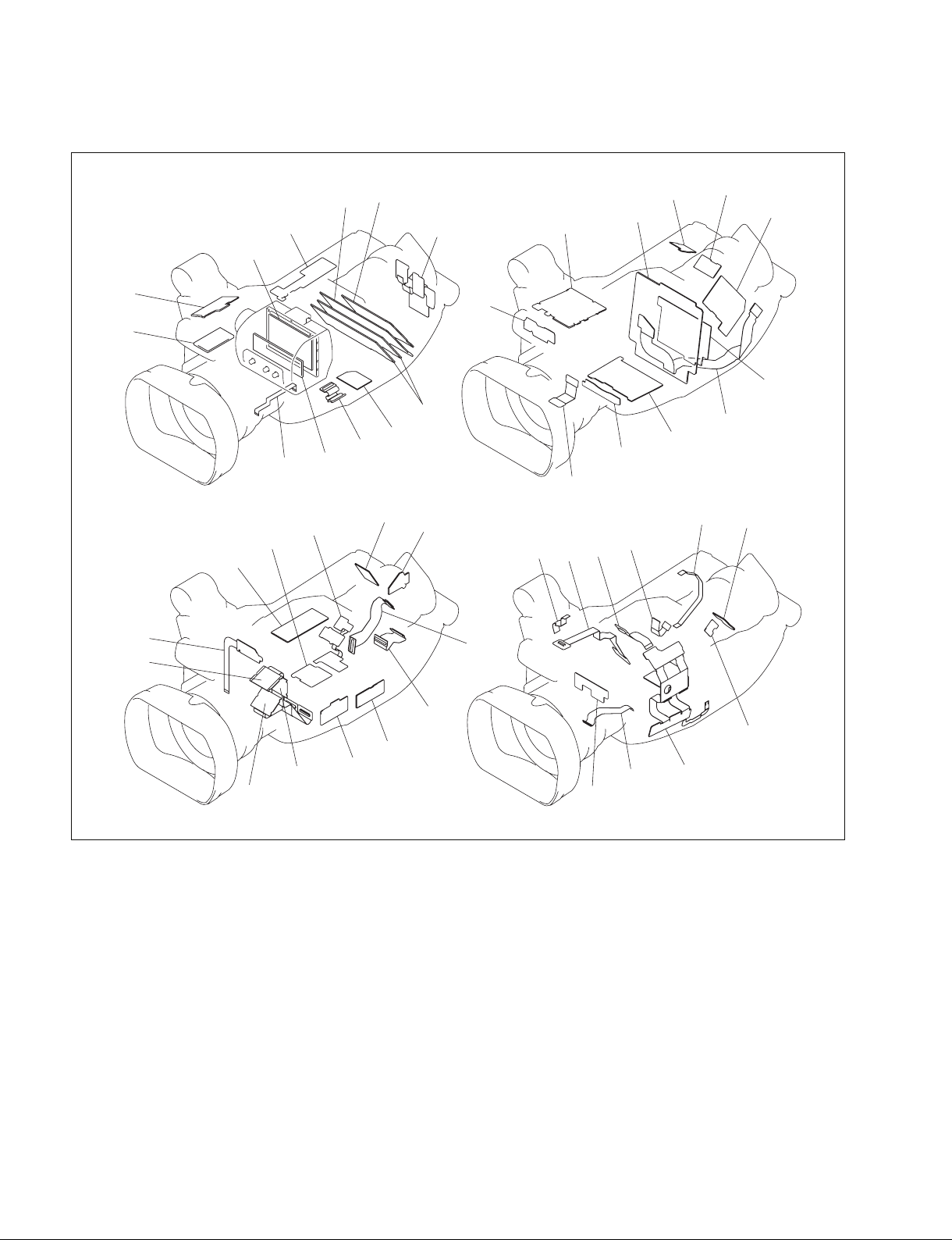
2. Replacement of Main Parts
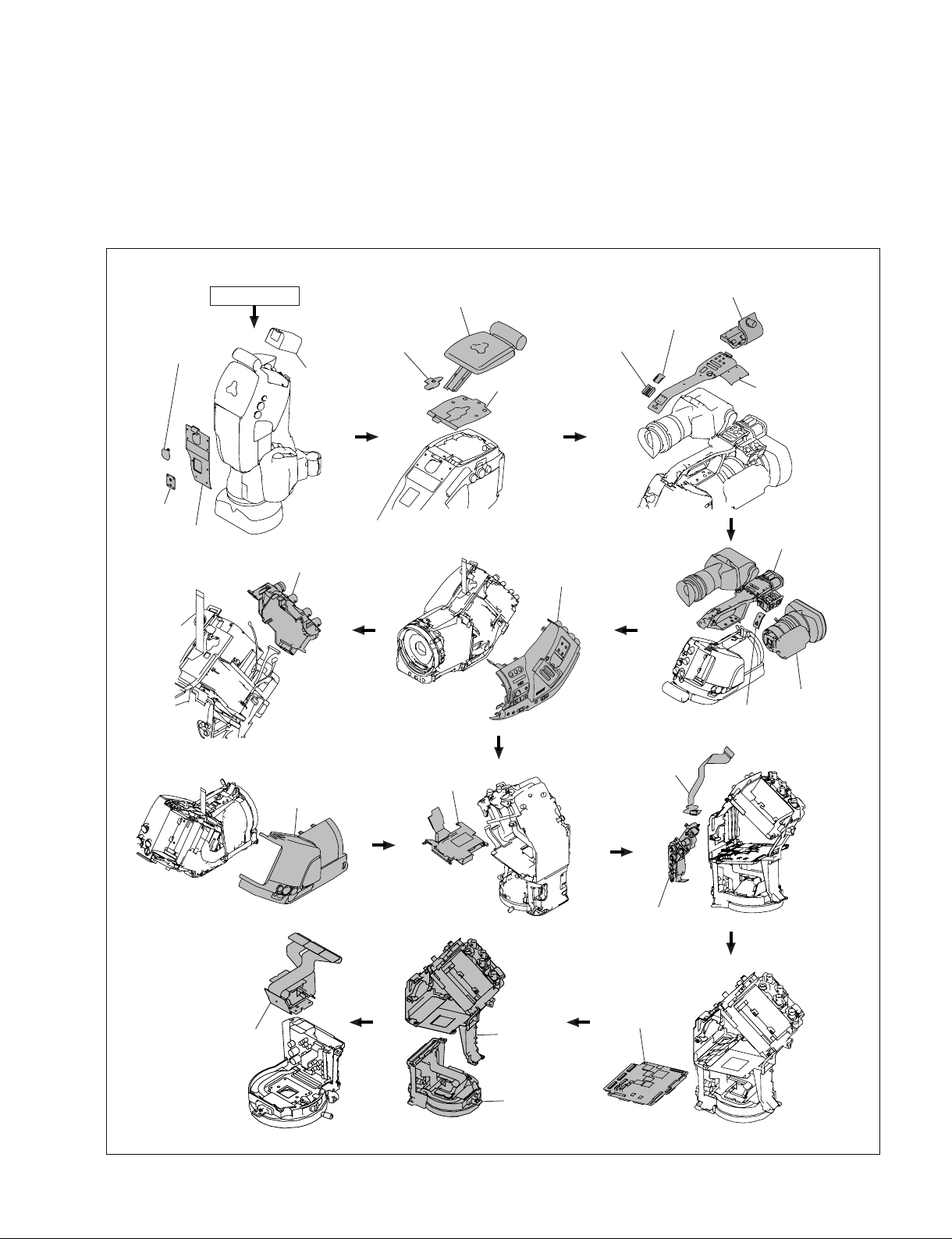
2-1. Outline of Replacement Procedures ...............................2-1
2-2. Replacement Procedures ................................................. 2-2
2-2-1. Lithium Battery ..................................................... 2-2
2-2-2. Bottom Panel .........................................................2-2
2-2-3. Pad Sub Assembly, Pad Cover ..............................2-3
2-2-4. LCD Assembly, CT-251 Board ............................. 2-4
2-2-5. Handle Top Cover Assembly ................................ 2-5
2-2-6. KSW-54 Board, Control Switch Block .................2-6
2-2-7. IF-1069 Board, LED-469 Board ...........................2-7
2-2-8. AXM-36 Board, HN-349 Board ............................ 2-8
2-2-9. Handle Assembly ..................................................2-9
2-2-10. Microphone Assembly ........................................ 2-10
2-2-11. Microphone Unit, MA-164 Board,
RM-214 Board ..................................................... 2-11
2-2-12. SWC-49 Board .................................................... 2-12
2-2-13. Inside Panel Assembly ........................................ 2-13
2-2-14. CN-3050 Board ................................................... 2-14
2-2-15. Connector Rear Assembly ................................... 2-15
2-2-16. ASW-66 Board, SW-1412 Board ........................2-16
2-2-17. SW-1410 Board ...................................................2-17
2-2-18. HN-344 Board .....................................................2-18
2-2-19. HN-343 Board, SWC-48 Board .......................... 2-19
2-2-20. SW-1411 Board ...................................................2-21
2-2-21. Outside Panel Sub Assembly .............................. 2-21
2-2-22. SW-1389 Board ...................................................2-22
2-2-23. Battery Case Assembly ....................................... 2-23
2-2-24. EX-DD Assembly ............................................... 2-24
2-2-25. CN-3023 Board ................................................... 2-26
2-2-26. RE-260 Board ...................................................... 2-26
2-2-27. EC-63 Board ........................................................ 2-27
2-2-28. PS-747 Board ...................................................... 2-28
2-2-29. TX-129 Board ..................................................... 2-29
2-2-30. Outside Connector Assembly ..............................2-30
2-2-31. DPR-289A Board ................................................ 2-31
2-2-32. Lens Mount Block ...............................................2-32
2-2-33. Prism Block Unit .................................................2-32
2-2-34. SE-923 Board ...................................................... 2-33
2-2-35. AU-318 Board .....................................................2-34
2-2-36. IR-42 Board ......................................................... 2-35
2-2-37. Replacing the Parts in the Lens Grip ................... 2-36
3. SERVICE Menu
3-1. SERVICE Menu List ...................................................... 3-1
3-2. SERVICE Menu Description .......................................... 3-3
3-2-1. Basic Menu Operations ......................................... 3-3
3-2-2. SERVICE Menu Structure .................................... 3-3
3-2-3. Displaying the SERVICE Menu ........................... 3-3
3-3. SERVICE Menu Description .......................................... 3-3
3-3-1. MAINTENANCE Menu ....................................... 3-3
3-3-2. RPN CORRECT Menu ......................................... 3-7
3-3-3. INFORMATION Menu ......................................... 3-8
4. Spare Parts
4-1. Notes on Repair Parts .....................................................4-1
4-2. Exploded Views ..............................................................4-2
4-3. Electrical Parts List .......................................................4-22
4-4. Supplied Accessories .................................................... 4-60
PMW-EX3
1
Page 6

5. Semiconductor Pin Assignments
6. Block Diagrams
Overall ............................................................................ 6-2
ASW-66 .......................................................................... 6-3
HN-337 ....................................................................... 6-3, 6
HP-144 ............................................................................6-3
LED-469 ......................................................................... 6-3
SW-1412 .........................................................................6-3
AU-318 ..................................................................... 6-4, 10
AXM-36 ...................................................................... 6-4, 9
HN-326 ..................................................................... 6-4, 10
HN-328 ........................................................................... 6-4
HN-343 ........................................................................... 6-4
HN-344 ..................................................................... 6-4, 10
HN-349 ....................................................................... 6-4, 9
KSW-54 ...................................................................... 6-4, 9
MA-164 ........................................................................... 6-4
SWC-48 ....................................................................6-4, 10
BI-202 .............................................................................6-5
BI-203 .............................................................................6-5
BI-204 .............................................................................6-5
DPR-289A ..........................................................6-5, 6, 7, 8
CN-3050 ......................................................................... 6-6
EC-63 ..............................................................................6-6
HN-347 ....................................................................... 6-7, 8
JK-81 ........................................................................... 6-7, 8
JK-84 ........................................................................... 6-7, 8
CT-251 ............................................................................6-9
HN-348 ........................................................................... 6-9
IF-1069 ........................................................................... 6-9
RM-214 ...........................................................................6-9
SWC-49 ..........................................................................6-9
BP-42 ............................................................................ 6-10
HN-345 ......................................................................... 6-10
HN-346 ......................................................................... 6-10
IR-42 .............................................................................6-10
SE-923 .......................................................................... 6-10
SW-1389 .......................................................................6-10
SW-1410 .......................................................................6-10
SW-1411 .......................................................................6-10
CN-3024 ....................................................................... 6-11
TX-129 .......................................................................... 6-11
CN-3022 ....................................................................... 6-12
DC-146 ......................................................................... 6-12
PS-747 ...........................................................................6-12
RE-260 ..........................................................................6-12
CN-3023 ....................................................................... 6-13
RE-261 ..........................................................................6-13
7. Schematic Diagrams
ASW-66 .......................................................................... 7-2
AU-318 ........................................................................... 7-5
AXM-36 .......................................................................... 7-8
BI-202 .............................................................................7-9
BI-203 ...........................................................................7-10
BI-204 ...........................................................................7-11
BP-42 ............................................................................ 7-12
CN-3022 ....................................................................... 7-12
CN-3023 ....................................................................... 7-13
CN-3024 ....................................................................... 7-14
CN-3050 ....................................................................... 7-14
CT-251 ..........................................................................7-15
DC-146 ......................................................................... 7-15
DPR-289A .................................................................... 7-16
EC-63 ............................................................................7-46
HN-328 ......................................................................... 7-46
HN-343 ......................................................................... 7-46
HN-326 ......................................................................... 7-47
HN-337 ......................................................................... 7-47
HN-344 ......................................................................... 7-48
HN-345 ......................................................................... 7-48
HN-346 ......................................................................... 7-48
HN-347 ......................................................................... 7-49
HN-348 ......................................................................... 7-49
HN-349 ......................................................................... 7-49
HP-144 ..........................................................................7-50
IF-1069 ......................................................................... 7-50
IR-42 .............................................................................7-51
JK-81 .............................................................................7-52
JK-84 .............................................................................7-53
KSW-54 ........................................................................ 7-54
2
PMW-EX3
Page 7

LED-469 ....................................................................... 7-55
PS-747 ........................................................................... 7-55
MA-164 ......................................................................... 7-56
RE-260 ..........................................................................7-57
RE-261 ..........................................................................7-61
RM-214 .........................................................................7-64
SE-923 .......................................................................... 7-64
SW-1411 .......................................................................7-64
SW-1389 .......................................................................7-65
SW-1410 .......................................................................7-65
SW-1412 .......................................................................7-65
SWC-48 ........................................................................7-66
SWC-49 ........................................................................7-68
TX-129 .......................................................................... 7-69
Frame Wiring ................................................................7-77
8. Board Layouts
ASW-66 .......................................................................... 8-2
AU-318 ........................................................................... 8-2
AXM-36 .......................................................................... 8-3
BI-202 .............................................................................8-3
BI-203 .............................................................................8-3
BI-204 .............................................................................8-4
BP-42 .............................................................................. 8-4
CN-3022 ......................................................................... 8-4
CN-3023 ......................................................................... 8-4
CN-3024 ......................................................................... 8-4
CN-3050 ......................................................................... 8-4
CT-251 ............................................................................8-5
DC-146 ........................................................................... 8-5
DPR-289A ......................................................................8-5
EC-63 ..............................................................................8-7
HN-326 ........................................................................... 8-7
HN-328 ........................................................................... 8-7
HN-337 ........................................................................... 8-8
HN-343 ........................................................................... 8-8
HN-344 ........................................................................... 8-8
HN-345 ........................................................................... 8-8
HN-346 ........................................................................... 8-8
HN-347 ........................................................................... 8-8
HN-348 ........................................................................... 8-8
HN-349 ........................................................................... 8-9
HP-144 ............................................................................8-9
IF-1069 ........................................................................... 8-9
IR-42 ............................................................................... 8-9
JK-81 ............................................................................... 8-9
JK-84 ............................................................................... 8-9
KSW-54 ........................................................................ 8-10
LED-469 ....................................................................... 8-10
MA-164 ......................................................................... 8-10
PS-747 ........................................................................... 8-10
RE-260 ..........................................................................8-11
RE-261 ..........................................................................8-11
RM-214 .........................................................................8-12
SE-923 ..........................................................................8-12
SW-1389 .......................................................................8-12
SW-1410 .......................................................................8-12
SW-1411 .......................................................................8-12
SW-1412 .......................................................................8-12
SWC-48 ........................................................................8-13
SWC-49 ........................................................................8-13
TX-129 .......................................................................... 8-14
PMW-EX3
3
Page 8

Purpose of this manual
Related manuals
Manual Structure
The service manual is intended for use by trained system and service engineers, and
provides the information of maintenance and detailed service.
The following manuals are available in this model.
If this manual is required, please contact your local Sony Sales Office/Service
Center.
..
. Operating Instructions (Supplied with the unit)
..
This manual is necessary for application and operation (and installation) of this
unit.
..
. “Semiconductor Pin Assignments” CD-ROM
..
This “Semiconductor Pin Assignments” CD-ROM allows you to search for
semiconductors used in Broadcast and Professional equipment.
This manual contains a complete list of semiconductors and their ID Nos., and
thus should be used together with the CD-ROM.
Part number: 9-968-546-06
4
PMW-EX3
Page 9
Section 1
Service Overview
1-1. External Connectors
1-1-1. Signal Inputs and Outputs
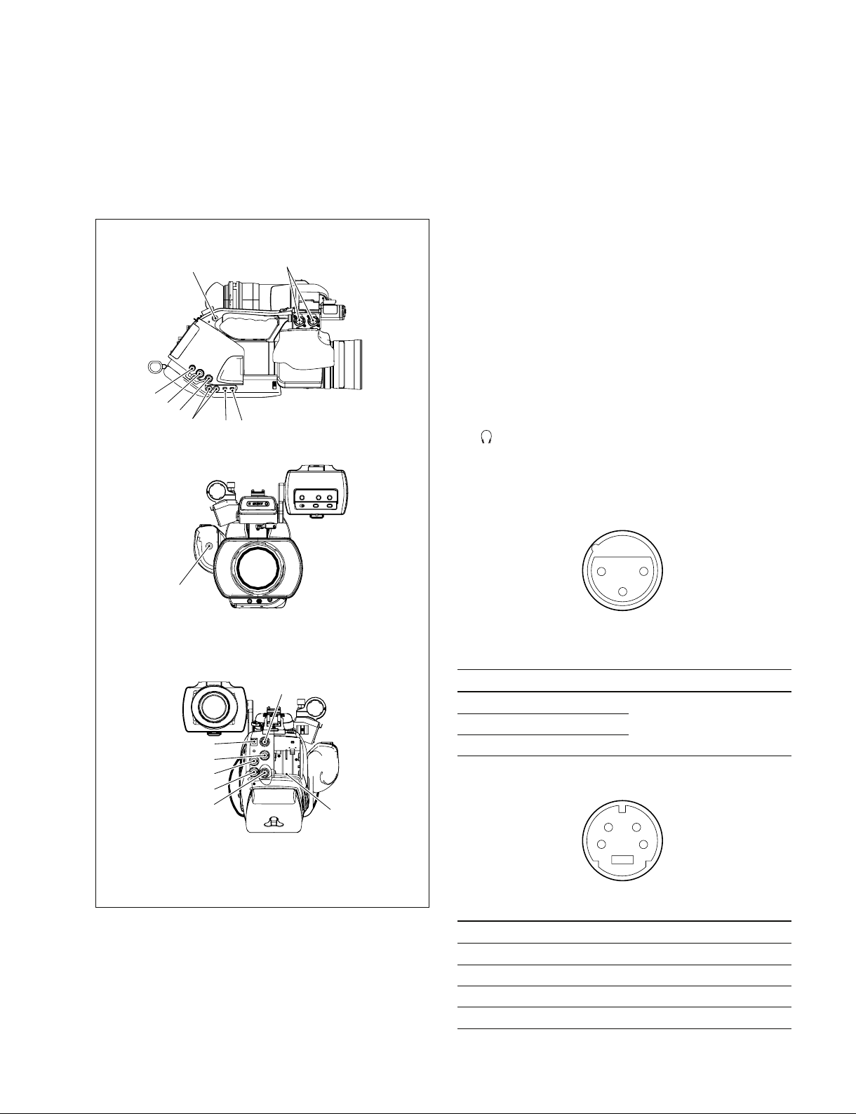
SIDE VIEW
7
!=
![
2
8
FRONT VIEW
6
9
0
1 SDI OUT : BNC type
SDI output signal
2 MONITOR OUT : BNC type
1.0 V p-p, 75 Z
3 TC IN : BNC type
0.5V to 18V, 10 kZ
4 TC OUT : BNC type
1.0 V p-p, 75 Z
5 GENLOCK IN : BNC type
1.0 V p-p, 75 Z
6 (HEADPHONES) : Stereo mini jack
Sound monitor, monaural/stereo selectable
_20.5 dBu (Reference level 16 Z loaded)
7 AUDIO IN CH-1, CH-2 : XLR (3P, Female)
REAR VIEW
!\
!5
3
4
!]
1
!;
2
__
_ EXT VIEW
__
1
3
__
_
__
(0 dBu = 0.775 V rms)
No. Signal I/O Specifications
1 MIC/LINE (G) __60 dBu/_50 dBu/_40 dBu/
2 MIC/LINE (H) IN +4 dBu, selectable
3 MIC/LINE (C) IN High impedance, Balanced
8 S-VIDEO OUT : S-video connector (4P)
34
12
__
_ EXT VIEW
__
No. Signal I/O Specifications
1 Y/C_GND _ GND
2 Y/C_GND _ GND
3 S-Y O S OUT (Y)
4 S-C O S OUT (C)
__
_
__
PMW-EX3
1-1
Page 10
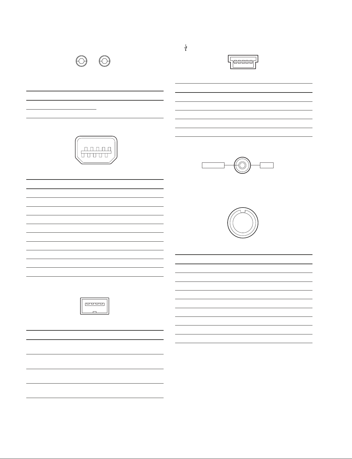
9 AUDIO OUT : RCA PIN
15
!= (USB) : Mini-B connector (5P)
1
__
_ EXT VIEW
__
2
__
_
__
No. Signal I/O Specifications
1 AUDIO CH-1 O _10 dBu
2 AUDIO CH-2 O
0 COMPONENT OUT : Mini D connector (10P)
19
210
__
_ EXT VIEW
__
__
_
__
No. Signal I/O Specifications
1 Y O COMPONENT (Y)
2 Y_GND _ Y GND
3 PB O COMPONENT (Pb)
4 PBPR_GND _ PBPR GND
5 PR O COMPONENT (Pr)
6NC _
7NC _
8NC _
9 SW_GND _
10 SW I
!- HDV : i.LINK connector (IEEE1394, S400) (4P)
14
__
_ EXT VIEW
__
No. Signal I/O Specifications
1TPB_ I/O Strobe on receive, data on
2TPB+ I/O Strobe on receive, data on
3TPA_ I/O Data on receive, strobe on
4TPA+ I/O Data on receive, strobe on
__
_
__
transmit B (_)
transmit B (+)
transmit A (_)
transmit A (+)
__
_ EXT VIEW
__
__
_
__
No. Signal I/O Specifications
1 VCC _ USB Vcc
2D _ I/O USB_
3D + I/O USB+
4ID _ NC
5 GND _ Ground
![ DC IN : 2P (DC JACK TYPE 4)
GNDEXT DC
__
_ EXT VIEW
__
__
_
__
!] REMOTE : (8P Female)
1
27
8
36
45
__
_ EXT VIEW
__
No. Signal I/O Specifications
1 TX RCP DATA (X) O SERIAL DATA OUT
2 TX RCP DATA (Y) O SERIAL DATA OUT
3 RX RCP DATA (X) I SERIAL DATA IN
4 RX RCP DATA (Y) I SERIAL DATA IN
5 DATA GND _ GND for VIDEO and DATA
6 UNREG +12 V O +11 V to 17 V
7 UNREG (GND) _ GND for UNREG
8 VIDEO (X) O 1.0 V p-p, Zo = 75 Z
CHASSIS GND _ CHASSIS GND
__
_
__
1-2
PMW-EX3
Page 11
!\ LENS REMOTE : (8P Female)
18
2
7
3
4
6
5
__
_ EXT VIEW
__
__
_
__
No. Signal I/O Specifications
1 COMMON_V O GND
2 ZOOM I GND: WIDE 1.66V: STOP
3.33V: TELE
3 COMMON+V O 3.33V
4 COMMON I 1.66V
5 REC I GND: ON OPEN: OFF
6 RET I GND: ON OPEN: OFF
7 SW COMMON O GND
8 FRAME GND _
!; Battery : (5P)
12
__
_ EXT VIEW
__
No. Signal I/O Specifications
1 BATT (+) _ +11 to +17 V dc
2 BAT_SCL O
3 BAT_SDA I/O
4 BATT_ID_DATA I
5 BATT (_) _
345
__
_
__
PMW-EX3
1-3
Page 12
1-2. Location of the Printed Wiring Boards
#]
3
#.
6
$\
@,
#/
@-
@'
#-
!=
#;
@/
#'
@;
7
!\
!-
0
9
#,
@\
#=
!'
!;
!.
$/
@[
!]
#[
2
@]
![
1
$;
!,
#\
1 ASW-66 board
2 AU-318 board
3 AXM-36 board
4 BI-202 board
5 BI-203 board
6 BI-204 board
7 BP-42 board
8 CN-3022 board
9 CN-3023 board
0 CN-3024 board
!- CN-3050board
!= CT-251 board
4
5
![ DC-146 board
!] DPR-289A board
!\ EC-63 board
!; HN-326 board
!' HN-328 board
!, HN-337 board
!. HN-343 board
@/ HN-344 board
@- HN-345 board
@= HN-346 board
@[ HN-347 board
@] HN-348 board
$=
$-
8
@\ HN-349 board
@; HP-144 board
@' IF-1069 board
@, IF-1072 board
@. IR-42 board
#/ JK-81 board
#- JK-84 board
#= KSW-54 board
#[ LED-469 board
#] MA-164 board
#\ PS-747 board
#; RE-260 board
@.
@=
$]
#' RE-261 board
#, RM-214 board
#. SE-923 board
$/ SW-1389 board
$- SW-1410 board
$= SW-1411 board
$[ SW-1412 board
$] SWC-48 board
$\ SWC-49 board
$; TX-129 board
$[
1-4
PMW-EX3
Page 13

1-3. Circuit Description
1. CMOS Block System
BI-202/203/204 Board
The BI-202, BI-203 and BI-204 boards are the rigid
flexible boards connecting the CMOS image sensors (IC1)
to the DPR-289A board.
the following AUTO operations of the camera are detected.
The detected signals are sent to the CAMERA MICON
(camera u-processor: IC314).
. Auto white balance
. Auto black balance
. Auto focus
. Auto iris
. Auto knee
The CMOS image sensor receives the three primary colors
of R, G and B that are separated from the incoming light
by the prism. The CMOS image sensor converts the
incoming primary color to electric signal. The built-in 12bit column A/D converters then convert the R, G and B
analog video signals to the digital video signals respectively.
The electronic shutter, analog gain amplifier and black
level clamp functions are also provided in the above
boards.
The BI-202 board is for the R-channel signal, the BI -203
board is for the G-channel signal and the BI -204 board is
for the B-channel signal.
The CMOS image sensor receives the sync signal and the
serial communication signal from the DPR-289A board.
The 12-bit digital video signals that are supplied from the
CMOS image sensors pass through the EMI filters (FL1 to
FL4) and are input to the DPR-289A board.
Various decoupling capacitors and the damping resistors
are also mounted in the above boards.
IC3 of the BI-203 board is a temperature sensor that sends
the temperature data to the CAMERA MICON (camera u-
processor: IC314) on the DPR-289A board via I2C bus.
2. Camera Block System
DPR-289A Board
The DPR-289A board consists of the Camera Signal
Processor IC (IC100) and the CAMERA MICON (camera
u-processor: IC314) whereas the Camera Signal Processor
IC (IC100) performs various processing on the digital
video signal supplied from the CMOS image sensor, and
the CAMERA MICON (IC314) performs control of IC100
and other various controls such as control of the CMOS
image sensor and of lens. The output digital video (Y/C)
signal is sent to the next circuit the video (baseband video)
signal processing circuit.
The 12-bit digital video (RGB) signals supplied from the
CMOS block (BI-202, BI-203 and BI-204 boards) first
enter the camera signal processor IC (IC100). In the
camera signal processor IC (IC100), average value, peak
value of the RGB digital video signals that are required for
The digital video signal from the CMOS image sensor
enters first the selector circuit selecting either the digital
video signal from the CMOS image sensor or the internal
TEST signal. The output video signal from the selector
enters the compensation circuits consisting of the CMOS
imager-related compensation circuit and the lens-related
compensation circuit. The video signal then receives the
white balance processing, and the matrix signal and the
detail signal are added to the video signal. The video signal
then receives the pedestal control, knee compensation,
gamma correction and white/black clip processing. The
video signal finally enters the baseband processing IC
(IC400).
The pixel number conversion processing from 1920/1080
to 1440/1080 or 1280/720 is also performed inside IC100.
The CAMERA MICON (camera u-processor: IC314)
performs the overall control over the entire camera system
and is controlled by the camera system controller
(IC1600).
Peripheral ICs of the CAMERA MICON (camera u-
processor: IC314) are FLAH ROM (IC312) and SRAM
(IC313). The CAMERA MICON (camera μ–processor:
IC314) confirms the iris control and lens setup when the
analog I/F lens is installed.
3. Video Signal System
DPR-289A Board
The digital video (Y/C) signal output from the camera
signal processor IC (IC100) enters the baseband processing
IC (IC400).
The baseband processing IC (IC400) performs the overall
baseband processing of video and audio signals with a
single chip IC containing the various scaler functions
(supporting the multiple format outputs), various OSD
functions, PLL function (54 MHz → 74 MHz) and CPU.
The baseband processing IC (IC400) provides the following outputs:
. HD/SD-SDI (digital): To TX-129 board
. HD/SD Component (analog): To JK-81 board
. Composite (analog): To JK-84 board
. S-Video (analog): To JK-84 board
. LCD signal (digital): To IF-1072 board
PMW-EX3
1-5
Page 14

The input/output signals of the baseband processing IC
(IC400) are the following signals:
. MPEG encoder/decoder I/F signal (digital): To IC901
. Audio I/F signal (digital): To IC804
PAM memory (IC700, IC701).
Peripheral circuits of the built-in CPU are FLASH ROM
(IC603) and SDRAM (IC607).
The baseband processing IC (IC400) is controlled by the
system controller (IC1600). The LCD driver IC, SDI Copro, the audio system and the power save control of the
output systems are controlled by the built-in CPU inside
IC400.
4. Media Recording and Playback
DPR-289A board
Output from the baseband processing IC (IC400) is input
into the MPEG encoder/decoder (IC901).
The MPEG encoder/decoder (IC901) is the single-chip
MPEG Codec IC that encodes and decodes both the highquality HD video signal and audio signal in real-time. It
has various interfaces with signals such as MPEG video,
video input/output, MPEG audio, audio input/output, bit
stream input/output, and interface with the host.
IC901 output is then input into LSI (IC900) for AVIT
signal processing.
LSI (IC900) for AVIT signal processing contains the builtin CPU and has interfaces for DDR2 SDRAM memory
(IC1000, IC1001), PCI bus, PCI-Express bus, I/O for
IC901, and serial communication with system controller
(IC1600).
IC900 is also connected to the NOR-type Flash ROM
(IC1100) to read the CPU program in the IC900 during
initial startup.
LSI (IC900) for AVIT signal processing is controlled by
the system controller (IC1600), in the same way as other
main devices, and provides the following types of functions: video/audio stream control, access to the SxS
memory card, mass storage operations when connected to
USB and HDV device controls when connected to i-LINK.
Explanation of peripheral devices
<SxS memory card slot>
Two memory card slot boards (EC-63) are connected to the
dual channel PCI-Express signals coming from IC900
through a 0.5 mm pitch, 30-pin fine coaxial cables connected to CN1300 and CN1301.
Furthermore, dual channel USB host signals output from
USB host controller (IC1302) are connect to the EC-63
board through fine coaxial cables just as with the PCIExpress signals.
IC1302 is controlled by PCI bus from IC900.
<USB device controller>
USB device signal output from USB device controller
(IC1101) is connected to output board (JK-81) through the
both-sided flexible board (HN-347) from CN1805 connector, and then it is connected to USB Mini-B connector
(CN6) on the JK-81 board.
IC1101 is controlled by the dedicated bus from IC900.
If there is no USB connection, the power supply for
IC1101 drops off.
<i-Link controller >
The i-Link signal output from the i-Link controller
(IC1200) passes through the both-sided flexible board
(HN-337) from the CN1803 connector. Then, the signal is
sent from CN3 on HN-337 to the i-Link connector board
(CN-3050) through the shielded wire, and connected to the
4 Pin i-Link connector (CN3) on the CN-3050 board.
IC1200 is controlled by the PCI bus from IC900.
5. Audio system
This overview explains the audio system according to the
audio block diagram shown in Fig. 1.
MA-164 board
The MA-164 board contains a built-in microphone unit.
The MA-164 board amplifies the audio signal with the
microphone bias power supply and head amplifier (Q5,
Q7, and Q9, and Q6, Q8, and Q10). It provides the balanced output for the audio signal.
AXM-36 board
The AXM-36 board is a connector board on which XLR
(3-pin) connector for external LINE/MIC input and the
[LINE/MIC/MIC +48V] input selection switch for two
channels are mounted on this connector board.
KSW-54 board
This board performs the read and tally controls for the
switch on the handle. The audio signal block relays the
audio signal between the MA-164 board and AXM-36
board.
HN-328/HN-343/SWC-48/HN-344 flexible board
This board relays the audio signal between the KSW-54
board and the AU-318 board.
AU-318 board (Audio block)
This board controls the analog audio input signal processing, as well as microphone +48 V power supply and serial
signal.
(RTC is also built on this board, but the explanation has
been omitted here.)
1-6
PMW-EX3
Page 15
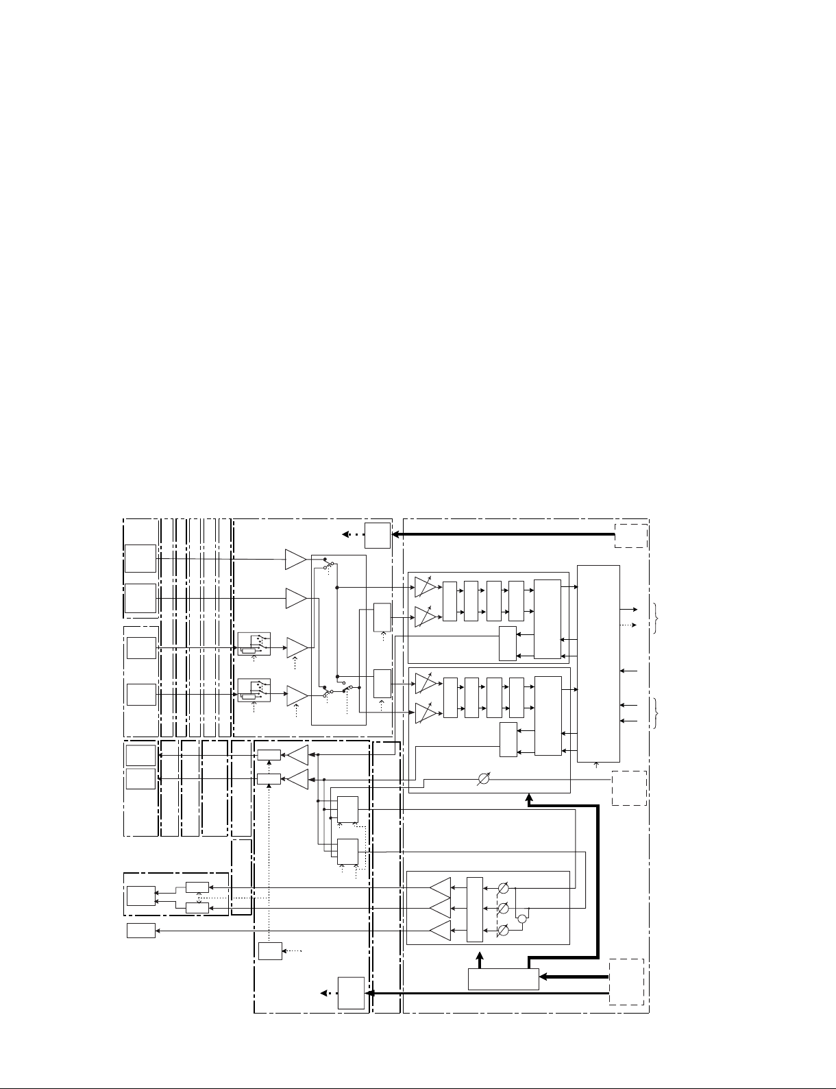
. Audio signal from the built-in microphone on the MA-
164 board is input to the balanced input amplifier IC101
and IC201 of this board. Output of the balanced amplifier is connected to the analog switch (IC105, IC205) for
switching between [INT/EXT].
. The DC-DC converter (IC1, Q1) for microphone power
+48 V is built-in, and when EXT MIC +48 V is going to
be supplied, the EXT MIC +48 V is supplied by the
switch (Q301, Q302, Q321 and Q322).
. The audio input signals from MIC and LINE are input to
a common circuit that receives both of the MIC input
level (_8 dBu to _65 dBu) and the LINE input level (+4
dBu). The input attenuator is inserted in the circuit
switch (Q103 to Q105, Q203 to Q205) as required. This
audio input signal is received by the balanced input
amplifier (IC102, IC202) that performs amplification of
0/+12 dB and switching (Q110, Q111, Q210, Q211) in
accordance with the level that is set by INPUT TRIM.
After that, the audio signal is connected to the [INT/
EXT] switch (IC105, IC205).
. The [INT/EXT] switch (IC105, IC205) performs not only
the INT/EXT switching but also performs the input
channel mode selection [CH1/ (CH1/CH2)].
. SEL/AMP (1, 2) is a signal selector and buffer amplifier
to perform AGC link.
. Serial control
2
C control signal from Display Block (T-one) is
The I
converted into GPI, and performs switching such as
[INT/EXT], [LINE/MIC/MIC+48], [CH1/ (CH/CH)],
and AGC [Linked/Separated] for CH1 and CH2.
DPR-289A board (Audio block)
The AU-318 board is comprised of two pieces of the
Audio Codec IC and the C-PLD.
. Audio Codec (IC800, IC801)
The analog audio signal from the AU-318 board is
connected to IC800 and IC801 that are the Audio Codec
(PGA, ADC, DSP, Digital IF, headphones amplifier,
speaker amplifier are built on one chip and the parameters are set with I
2
C).
The Input TRIM (PGA) functions in the [MANUAL]
mode, and AGC functions in the [AUTO] mode to
control the audio signal level. The analog signal after
MA-164
Q5,Q7,Q9
INT MIC1
with
HEAD AMP
+12dB
Q6,Q8,Q10
INT MIC2
with
HEAD AMP
+12dB
MIC/LINE1
(XLR)
MIC/LINE 2
(XLR)
AXM-36
AV Monitor
Out1
(Line Out1)
AV Monitor
Out2
(Line Out2)
JK-84
HP-144
HP OUT
(PHONE
MINI)
CN2
SPEAKER
KSW-54
JK-81
HN-328
HN-347
Q1
MUTE
Q2
MUTE
HN-343
Q103 to Q105, Q301,Q302
HN-344
SWC-48
+48V /MIC / LINE -1
Q203 to Q205,
Q321,Q322
+48V /MIC / LINE -2
(2/2)
DPR-289A
AU-318
-24
-24
MUTE AMP
MUTE
HN-337(2/2)
LED-469
PWR or
ASW-66
DET
INT/EXT1,INT/EXT2
MIC/LINE/+48V-1,
MIC/LINE/+48V-2,
COPY1to2, LINK2to1, LINK1to2
BAL
AMP
IC101
INT/
EXT 1
BAL
AMP
IC201
IC105,
BAL
AMP
IC102
Q110,
Q111
(GAIN SEL
CH1)
BAL
AMP
IC202
Q210,
Q211
(GAIN SEL
CH2)
AMP
MONI1-1,2-1,
MONI2-2,2-1,
BEEP,
MUTE
IC101,
IC102(2/2)
MONI CH2-2
MONI CH2-2
MUTE
IC205
INT/EXT 2
+48V
+48V
Q103
Q104
Q100 to Q102
IIC to
CH1 CH1/CH2
IC100,
IC102(1/2)
SEL/
MIX1
MONI CH-1
MONI CH2-1
SEL/
MIX2
IC104, IC105
GPIO
BEEP
GPIO
IC401 to
IC404
Linked/
Separated
Linked/
Separated
IC103,
IC104
SEL/
AMP1
IC203,
IC204
SEL/
AMP2
HN-337
(1/2)
DPR-289A
(1/2)
PGA
GAIN
PGA
GAIN
PGA
GAIN
PGA
GAIN
A/D
A/D
AMP
AMP
AMP
Fig. 1. Audio block diagram
IC800(1/2)
FIL AGC LVL
D/A
FIL AGC LVL
D/A
IC801
IC800(2/2)
MIX
AMP
IC800
IC803
I2C MPX
(DEVICE CONTROL)
I2S
AUDIO IF
I2S
AUDIO IF
AUX IN( L)
AUX IN( R)
+
MONITOR LEVEL
I2C
I2C
I2C
Digital Audio
OUT 1
Digital Audio
IN 1 or 3
CLOCK DIV
(1fs,64fs,256fs)
GAIN MAKE
OUT 2
Digital Audio
IN 2 or 4
CLOCK DIV
(1fs,64fs,256fs)
IC804
C-PLD
DP_O_CAM_
AU_DT12O
(DP_O_CAM
_AU_DT34O)
CLOCK DIV
(1fs,64fs,256fs)
DP_I_CAM_A
U_DT12O
DP_I_CAM_A
U_DT34O
LINE 3/4
Display
Block(T-on)
BEEP
(T-one)
Display
Block
(T-one)
Recording
signal
Playback
signal
PMW-EX3
1-7
Page 16

level adjustment is converted to the digital signal with
the ADC.
The digital signal receives the audio level control
processing from the DSP. After the audio signal receives
the [Wind Filter] (on/off) processing, the digital signal is
output for audio recording.
Playback output (including EE) is the digital signal that
is connected to Audio Codec where it is converted to the
analog signal with DAC and output to the ASW-66
board.
Furthermore, the audio signal that is processed for audio
monitoring in the ASW-66 board is connected to the
headphones amplifier and speaker amplifier through the
monitor level control from the AUX input of IC800.
. C-PLD (IC804)
After the digital signal output signal from the Audio
Codec is amplified by +12 dB, it is supplied to the
Display Block (T-one). C-PLD (IC804) also receives the
playback output signal from the Display Block.
The playback system selects CH1/CH2 or CH3/CH4,
connects EE, and connects TEST TONE from the
Display Block depending on the data.
Furthermore, C-PLD divides the clock signal that is
supplied from the Display Block to Audio Codec.
. Serial control
The I2C control from Display Block (T-one) selects
either IC800 or IC801 for the target with I2C MPX and
sets the register of IC800 or IC801.
HN-337 flexible board
It relays the audio signal from the DPR-289A board to the
ASW-66 board.
ASW-66 board (Audio block)
. Analog output from the DPR-289A board Audio Codec
is buffered by IC103 and is output to the A/V connector
after passing through the audio MUTE control.
. Analog output from DAC on the DPR-289A board re-
enters into the AUX input of the DPR-289A board
AUDIO CODEC after passing through the monitor
selector/mixer (IC100, IC101, IC102), and becomes the
monitor signal.
. Serial control
I2C control signal from Display Block (T-one) is output
at GPI, and performs the switching between MONITOR
[CH1/CH2] / [CH1+CH2] / [CH1] / [CH2] for CH1 and
CH2 respectively, and at the same time controls the
BEEP on/off.
JK-84 board (Audio block)
This is the connector board. The audio output from the
ASW-66 board is connected to RCA PIN connector.
HP-144 board (Audio block)
The headphones output signal is connected to the headphones jack of the DPR-289A board.
The headphones output is muted by the MUTE (Q1, Q2).
Switch/Volume control/Menu panel (Audio
controller block)
Operation panel functions relating to audio signal are built
into the following blocks.
ASW-66 board (Audio block)
For CH1 and CH2, the switches [INT/EXT] and [AUTO/
MANUAL] are connected to PIO of CPU (IC106), and the
volume control [AUDIO LEVEL] is connected to ADC of
CPU (ICl06).
KSW-54 board (Audio block)
The switch [LINE/MIC/MIC+48] on the AXM-36 board is
connected to PIO of CPU (IC100) for CH1 and CH2
respectively. The switch [MONITOR (AUDIO) +/_] that
is common to CH1 and CH2 is connected to PIO of CPU
(IC100).
MENU processing
(1) Audio Input
. CH1, CH2 [INPUT TRIM]: _8 dBu to _65 dBu
. CH1, CH2 common [AGC Link]: Linked/Separated
. CH1, CH2 [WIND FILTER]: ON/OFF
. CH1, CH2 common [EXT CH Select]: [CH1] /
[CH1/CH2] selection
(2) Audio Output
. [MONITOR CH]: [CH1/CH2] / [CH1+CH2] /
[CH1] / [CH2] selection
. [Alarm Level]: 0 to 10
. [Beep]: ON/OFF
. [BARS]: TEST TONE (DPR-289A board Display
Block internal processing)
6. System Control
DPR-289A board
The 32-bit RISC CPU (ARM) with ARM core is built-in as
the system controller (IC1600).
It has the peripheral interface functions of SDRAM, USB,
SCI, and I2C. It operates on a 27 MHz clock (X1600).
FLASH ROM (IC1603), SDRAM (IC1604), and EEPROM (IC1703) are mounted as the peripheral ICs.
It performs the system control through serial communication with IC314 of the camera block system, IC400 of the
video signal system, and IC900 of the media recording/
playback system.
1-8
PMW-EX3
Page 17

Main functions of the system controller and
peripherals
(1) Reading operation switch information
Reading the switch information and the LED control
are performed by I2C bus communication with each
sub-microprocessor.
. Handle switch: IC100 on the KSW-54 board
. Inside panel front switch: IC601 on the SWC-48
board
. Rear panel switch: IC106 on the ASW-66 board
. Power supply switch: IC1001 on the RE-261 board
(2) Watch IC (RTC) control
The watch IC (IC50) is built onto the AU-318 board.
The watch IC (IC50) is backed up by a lithium coin
battery, and the current time is read or set via IC601 on the
SWC-48 board.
(3) Infrared remote control demodulation
The RM-214 board has an IC (IC1) for infrared remote
control signal demodulation, and it receives the command
codes via IC100 on the KSW-54 board.
(4) Info-Battery communication
The Info-Battery of SM bus specifications is supported.
The serial terminal of the battery connector is connected to
IC1001 on the RE-261 board. This IC1001 reads the
battery authentication, battery type, remaining power, and
other information and send them to the system controller
via I2C bus communication.
(5) Power supply voltage detection
The power supply voltage at the DC IN connector is
measured by the A/D port on IC1001 on the RE-261 board,
and it is posted to the system controller as the input voltage
value.
(6) Power system control
IC1001 on the RE-261 board checks that the power switch
on the PMW-EX1 is turned ON, and turns on the system
controller of IC1600. After that, it controls the power for
each circuit block according to the system controller.
The system controller controls the respective power supply
systems in the RE-260 and RE-261 boards according to the
operation mode of the device, via the power supply uprocessor on the RE-261 board.
By turning off the power systems to unnecessary circuits
blocks, power can be saved.
(7) 700P communication
The serial communication driver (IC803) is mounted on
the TX-129 board.
Serial communication with the remote control unit connected to the REMOTE connector is performed.
7. SDI/GENLOCK/TC IN/TC OUT
TX-129 board
(1) SDI output
This board receives the parallel video signal with FPGA
(IC100) and IC500 and outputs the SDI signal.
Furthermore, it performs audio or timecode embedding.
The video and audio signals are supplied from CN400 on
the DPR-289A board to CN100 on the TX-129 board with
a 0.4 mm pitch, 40-pin fine coaxial cable.
The power voltages are supplied from CN401 on the DPR289A board to CN700 on the TX-129 board with a 15-pin
harness.
Output SDI signals are supplied to CN500.
Output SDI signals are then supplied from CN500 to the
coaxial connector via the mini coaxial connector and mini
coaxial cable.
The PLL circuit is used to reduce jitter of the HD-SDI
clock signal.
The FPGA (IC100) is controlled by IC400 on the DPR289A board through 4-line serial communication.
The FPGA program is stored in the IC203 ROM, and
JTAG can be used to overwrite the data from IC1600 on
the DPR-289A board.
When not using SDI, the power to cable driver inside
IC500 is turned off.
(2) GENLOCK
In IC902, sync signal separation is performed for GNELOCK. The separated sync signal enters IC400 on the
DPR-289A board where phase is compared by the internal
counter of IC400 and by IC521 to control the VCXO
(X500).
(3) TC IN/TC OUT
IC900, IC901, and IC907 reshape the waveform of the
time code connected to the TC IN connector and input it to
IC100.
IC903 is the external output circuit for the time code OUT
signal, which outputs the signal to the TC OUT connector.
They communicate with the FPGA (IC100) through the 4line serial interface on the DPR-289A board.
PMW-EX3
1-9
Page 18

8. Power supply system
RE-260/261 board
This board is comprised of the power supply circuit and
the POWER SUPPLY MICON (power supply u-processor:
IC1001 on the RE-261 board).
However, part of the low-voltage power supply is mounted
on the DPR-289A board.
(1) Input power supply (UNREG) system operations
When the UNREG power is input, the EVER power state
is established.
In this state, the ON/OFF state of the Power switch can be
recognized.
If the POWER SUPPLY MICON (power supply uprocessor: IC1001) recognizes that Power switch is ON,
the power is turned on for the system control system and
the POWER SUPPLY MICON (power supply u-processor:
IC1001) controls the power supply for each block according to the system controller (DPR-289A board: IC1600).
The normal value for the input power supply (UNREG) is
in the range of about +10.5 V to +18 V.
. Battery/EXT-DC select
Input power comes in two systems: Battery and EXTDC. This switch monitors the input voltage for each
input and automatically switches the circuit settings with
priority given to EXT-DC.
. Input overvoltage protection
If the voltage is too high in the UNREG power supply,
the overvoltage protection circuit starts operating around
the set value of +17.9 V, and the camera shuts down.
When the input power supply voltage to this circuit
becomes less than +17.9 V, the power supply immediately switches on with automatic recovery.
. Input low-voltage protection
If the voltage is too low in the UNREG power supply,
the low-voltage protection circuit starts operating around
the set value of +10.5 V according to the control by the
POWER SUPPLY MICON (power supply u-processor:
IC1001), and the camera shuts down. When the input
power supply voltage becomes higher than +10.5 V, the
power supply immediately switches on with automatic
recovery according to the control by the POWER
SUPPLY MICON (power supply u-processor: IC1001).
. Overcurrent detection
The overcurrent detection circuit is comprised of IC308
on the RE-260 board. The setting value is approximately
4.3 (A). Even after clearing IC308 after overcurrent
detection, automatic recovery is not performed and the
power must be turned on again.
1-10
. Power supply reverse connection protection
If the input power has reverse voltage, Q301 on the RE260 board is immediately turned off and UNREG power
is stopped on the GND side, and the protection function
works.
(2) DC/DC converter function
The power supply output is divided into 25 systems, which
are separated into four blocks as seen below.
. CMOS/camera block system, 7 systems
(+4.6 V, +3.1 V, UNREG, etc.)
. Audio/video signal system, 7 systems
(+13.5 V, _4.6 V, +4.6 V, etc.)
. System controller system, 5 systems
(+4.6 V, +3.1 V, +2.5 V, etc.)
. Media recording/playback system, 6 systems
(+3.1 V, +2.5 V, +1.8 V, etc.)
The sequence control (powering up and powering down)
for the power supply system is controlled by the POWER SUPPLY MICON (power supply u-processor:
IC1001) for the respective power supply blocks of each
block.
By turning off the power for each block according to the
operation mode (camera mode or media mode), the
optimal power consumption for each operation is
achieved.
. Short-circuit protection for each power supply system
The circuit settings monitor each output voltage or
current for each power supply system and operate the
protection circuits per block.
Even after the protection circuit is cleared, automatic
recovery is not performed and the power must be turned
on again.
Even after short-circuit is cleared, the protection circuit
does not recover automatically and the power must be
turned on again.
Battery information functions
. Battery authentication function
The authentication function checks whether the battery is
of the specified type. This helps prevent one cause of
major accidents when using batteries as a power supply.
If the attached batter is not the specified type of batter,
the camera immediately turns off.
. Battery Info function
In an intelligent (specified) battery, the battery can
monitor information, such as how many times the battery
has been recycled or the internal temperature for the
battery. This helps provide detailed information about
the battery, including whether the battery is damaged or
how long the life is, in order to provide optimal operations.
PMW-EX3
Page 19

1-4. Service Tools/Measuring Equipment List
1-4-1. Service Tools
Part No. Name Usage/Note
Commercially available Grayscale chart Reflective type (16 : 9), Camera adjustment on market
Commercially available Star chart Reflective type, camera adjustment on market
J-6394-080-A Grayscale chart Transparent type (16 : 9), Camera adjustment on market
J-6029-140-B Pattern box PTB-500 Camera adjustment
* Mini USB cable For firmware version-upgrade
3-292-755-01 XLR JIGU For removing the mounted circuit board
* : This cable is supplied with PMW-EX3.
1-4-2. Measuring Equipment
Use the calibrated equipment or equivalent as listed below for the adjustments.
Equipment Model name
Oscilloscope Tektronix TDS3054 or equivalent (150 MHz or more)
HD waveform monitor LEADER ELECTRONICS CORP.LV5152DA or equivalent
Frequency counter Advantest TR5821AK or equivalent
Digital voltmeter Advantest TR6845 or equivalent
Color monitor Sony HDM-20E1U/14E1U/14E5U or equivalent
Luminance meter Konica Minolta LS-110 or equivalent
PMW-EX3
1-11
Page 20
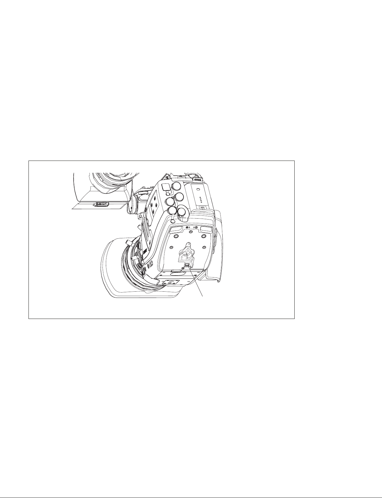
1-5. Firmware Upgrade
Upgrade the firmware for the PMW-EX1 through a USB connection to a computer.
For detailed information about the upgrade procedure, check the readme file that comes with the upgrade
software.
For inquiry or comments about the firmware upgrade, please contact your local Sony Sales Office/Service
Center.
Firmware Upgrade Procedure
Download the software for the new firmware upgrade onto the computer before starting these operations.
1. Check that the power switch on the PMW-EX3 is turned OFF.
2. Remove the pad sub assembly and pad center cover. (Refer to Section 2-2-3.)
USB maintenance connector
3. Use the USB connector that comes with the PMW-EX3 to connect the computer and the USB
maintenance connector.
4. Switch the power switch to CAMERA and turn the power ON.
5. Run the software for the firmware upgrade on the computer.
6. When the upgrade is complete, turn OFF the power and remove the USB cable.
7. Attach the pad sub assembly and pad center cover.
When the PMW-EX3 is connected to the computer for the first time, the driver software will need to be
installed into the computer. For more details, check the readme file that comes with the upgrade software.
1-12
PMW-EX3
Page 21
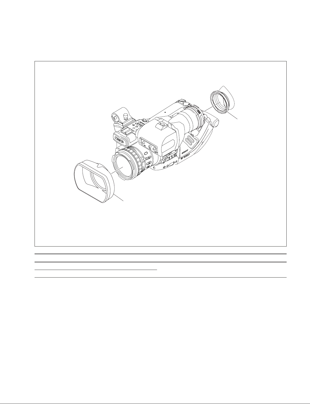
1-6. Recommended Replacement Parts
This section describes the recommended replacement parts and recommended replacement time.
2
1
ID Part name Sony part No. Recommended replacement timing
1 Lens hood 4-110-064-01
2 I cup 3-878-208-02
Check for deformation and deterioration from time to time.
Replace it as necessary.
PMW-EX3
1-13
Page 22

1-7. Note on Service
1-7-1. Requirements on Replacement of
Boards or Parts
This section explains the necessary setups required when
replacing boards or parts.
1. When any of the following boards is replaced, upgrade
the firmware version.
All data are written at once when upgrading the
firmware version. (Refer to Section 1-5.)
1-7-2. Note on Replacement of Parts on the
Board
1. The BI-202, BI-203 and BI-204 boards cannot be
replaced on the board-level service or part-level service.
If parts become defective, replace the entire CMOS
block.
2. Parts labels also cannot be replaced in the DPR-289A
board.
If parts become defective, replace the entire mounted
board.
Board name Ref. No.
DPR-289A IC312, IC603, IC1100, IC1603
KSW-54 IC100
SWC-48 IC601
ASW-66 IC106
RE-261 IC1001
TX-129 IC203
2. Adjusted values are stored in the following boards and
parts. The values need to be readjusted when they are
replaced.
Board/part name Ref. No.
DPR-289A
CMOS block IC312/DPR-289A board
LCD module
*1: The adjusted values for the CMOS block and the LCD module are
*2: The adjusted values for the LCD module are stored in the LCD module,
*1
*2
stored in the DPR-289A board.
but the adjusted values need to be copied to the DPR-289A board.
IC202/IF-1072 board, IC603/DPR289A board
3. The user setting values are stored in IC1703 on the
DPR-289A board. The user data must be stored
(Restore) in SxS before replacing the board and it must
be read (Recall) after replacing the board.
1-7-3. Description of Number Seal on the
Prism
The number seal is put in the prism unit, the serial number
of prism unit.
Every prism unit has its own number called prism serial
number.
1-7-4. Memory Backup Battery
For replacing the battery, refer to “Backup Battery” of the
“Appendixes” in the Operating Instructions.
When the backup battery is replaced, the date and time in
the internal clock need to be set. Refer to “Setting the
Clock” of the “Preparations” in the Operating Instructions.
1-7-5. Unleaded Solder
Boards requiring use of unleaded solder are printed with a
lead free mark (LF) indicating the solder contains no lead.
(Caution: Some printed circuit boards may not come
printed with the lead free mark due to their particular size.)
: LEAD FREE MARK
1-14
m
. Be sure to use the unleaded solder for the printed circuit
board printed with the lead free mark.
. The unleaded solder melts at a temperature about 40 dC
higher than the ordinary solder, therefore, it is recommended to use the soldering iron having a temperature
regulator.
. The ordinary soldering iron can be used but the iron tip
has to be applied to the solder joint for a slightly longer
time. The printed pattern (copper foil) may peel away if
the heated tip is applied for too long, so be careful.
PMW-EX3
Page 23
1-8. Connector Location Diagram on
CN500
1
CN300
1
Board
The PWM-EX1 uses flexible card wires and coaxial cables
with connector. The following diagrams indicate the
location of each connector. The location of flexible card
cables are indicated by the circle number 1 and 2, while
the coaxial cables with connector are not indicated by the
circle number.
KSW-54 board (A side) KSW-54 board (B side)
1
CN4
1
CN5
ASW-66 board (A side) AU-318 board (A side)
CN100
1
CN1 CN2
22
AXM-36 board (A side)
1
CN3
CN-3024 board (A side)
2
CN6
DPR-289 board (A side) DPR-289 board (B side)
SW-1389 board (B side) SW-1410 board (B side)
SWC-48 board (A side)
1
CN700
SWC-49 board (B side) TX-129 board (A side)
1
CN100
CN100
CN1301
CN1300
CN601
1
CN1804
CN400
CN402
EC-63 board (A side) EC-63 board (B side)
CN2 CN1
IF-1069 board (A side )
CN5
1
CN4
1
PMW-EX3
IR-42 board (A side )
CN103
2
CN102
CN800
1
1-15
Page 24
1-9. Replacing the Flexible Card Wires
n
The flat cables, flexible card wires and boards are used to
connect between the following boards. Life of flexible card
wire will be significantly shortened if it is folded. Be very
careful not to fold the flat cables, flexible card wires and
boards.
The two types of different shape connectors are used in
this unit.
Because the direction of the flat cables, flexible card wires
and boards are different depending on the shape of the
connector, be careful when connecting the flat cables,
flexible card wires and boards.
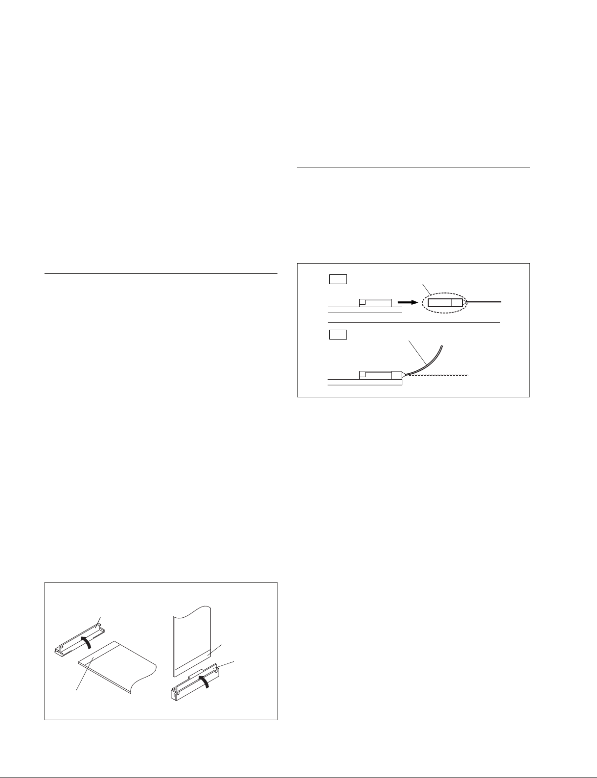
Disconnecting
1. Turn off the power.
2. Slide or lift up the portion A in the direction of the
arrow to unlock and pull out the flexible card wire.
Connecting
1-10. Replacing the Coaxial Cable with
Connector (Fine Pitch Coaxial Cable)
The PWM-EX1 uses coaxial cables with connector.
The following precautions must be observed when removing or connecting the coaxial cable with connector.
Note on Disconnecting
The coaxial cable with connector uses fine pitch coaxial
cables. Be careful when arranging the cable. When disconnecting the coaxial cable with connector, do not attempt to
remove by pulling the cable. Be sure to hold the connector
to remove.
Hold the connector to remove.
OK
Do not attempt to remove by pulling
NG
the cables.
m
. Do not insert the coaxial cable with connector sideways.
. Confirm that there is no stain or dust on the contact
surface of the coaxial cable with connector.
1. Slide or lift up the portion A in the direction of the
arrow and securely insert the flexible card wire into
the deep end of the connector.
2. Return the portion A to its original position and lock
the connector.
n
When connecting the flexible card wire, check the connector shape, and great care should be taken for the direction
of the contact surface or isolation surface (blue).
Connector : 1 Connector : 2
A
Isolation surface
(blue)
A
Isolation surface
(blue)
1-16
PMW-EX3
Page 25
Note on Connecting
When connecting the coaxial cable with connector, hold
the connector matching the polarity marks and insert the
coaxial cable straight into the corresponding connector.
Polarity marks
Yellow
Terminal side
Hold the connector to connect.
OK
Not to bend the cable.
NG
PMW-EX3
1-17
Page 26

1-11. List of Error Numbers on the LCD Display
Error numbers are displayed as E-XXXXX (X indicates a number).
Error No. Description Service action
15030 System error Repair the DPR-289A board or replace it.
17001 Abnormality in the Media ID data in Rewrite the media ID data in the EEPROM using
the EEPROM “ServiceNavi-EX”.
17002 The image processor block does not start up. Repair the DPR-289A board or replace it.
17003 The display block does not start up
17004 The media block does not start up
17005 Abnormality in the start-up process of
17006 Abnormality in the start-up process of
17007 Abnormality in the start-up process of
17014 Abnormality in lens communication Check the connection with the lens unit. If there is
17015 Abnormality in the media block Repair the DPR-289A or replace it.
17016 Abnormality in obtaining the lens switch Check the connection with the lens unit. If there is
17017 Internal error in the media block Repair the DPR-289A board or replace it.
or
4XXXX
the image processor block
the display block
the media block
no defect, replace the lens unit.
no condition defect, replace the lens unit.
1-12. Servicing software “ServiceNavi-EX”
Servicing software “ServiceNavi-EX” is required for electrical adjustment and self diagnosis.
For how to obtain the “ServiceNavi-EX”, contact your local Sony Sales Office/Service Center.
1-18
PMW-EX3
Page 27
Section 2
Replacement of Main Parts
2-1. Outline of Replacement Procedures
. The following figures show the flow for removing the main parts. Refer to Section 2-2 for details of the
replacement procedures.
Microphone
holder assembly
Spring
Handle assembly
Button
battery lid
Bracket
(tripod)
Bottom
panel
START
Battery
Connector rear
assembly
Pad sub assembly
Pad center
cover
Accessory
shoe
Pad cover
Inside panel
assembly
Handel top cover
assembly
Prism block
unit
Outside panel
sub assembly
TX block
Main frame
block
Lens mount
block
Lens
Front cover handle
HN-337 board
Out side connector
assembly
DPR-289A
board
PMW-EX3
2-1
Page 28
2-2. Replacement Procedures
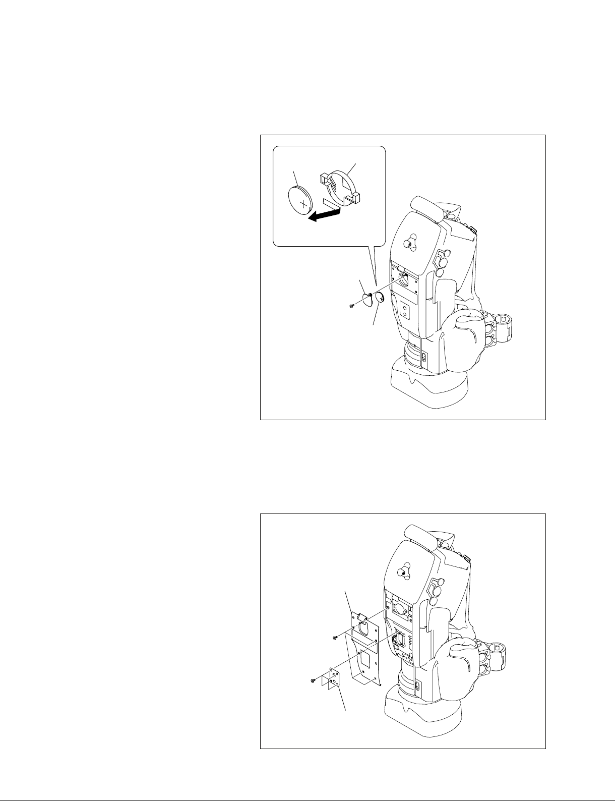
2-2-1. Lithium Battery
1. Loosen the screw, and remove the button
battery lid.
2. Remove the lithium battery.
Lithium battery
Battery holder
Lithium battery removal
Button battery lid
M2 x 4
Lithium battery
3. Reinstall the lithium battery by reversing the
steps of removal.
2-2-2. Bottom Panel
1. Remove the button battery lid. (Refer to
Section 2-2-1.)
2. Remove the four screws, and remove the
bracket (tripod).
3. Remove the four screws, and remove bottom
panel.
4. Reinstall the removed parts by reversing the
steps of removal.
Bottom panel
M2 x 4
M2 x 6
Bracket (tripod)
2-2
PMW-EX3
Page 29
2-2-3. Pad Sub Assembly, Pad Cover
1. Press the pad stopper in the direction of the
arrow A, while the pad stopper is being
unlocked, lift up the pad sub assembly in the
direction of the arrow B.
2. Remove the screw, and remove the pad
center cover.
3. Press the pad stopper in the direction of the
arrow A, while the pad stopper is being
unlocked, remove the pad sub assembly in
the direction of arrow B.
4. Remove the four screws, and remove the pad
cover.
Pad sub assembly
B2.6 x 6
Pad center cover
B
A
Pad stopper
M2 x 4
5. Reinstall the removed parts by reversing the
steps of removal.
Pad cover
PMW-EX3
2-3
Page 30
2-2-4. LCD Assembly, CT-251 Board
1. Remove the four screws, and remove the
display plate and the LCD cover.
2. Remove the four screws of the LCD assembly.
3. Disconnect the coaxial cable with connector
from the connector, and remove the LCD
assembly.
n
The coaxial cable with connector uses the
fine pitch coaxial cable. Be careful when
arranging the harness. When disconnecting
the coaxial cable with connector, never
remove it by pulling the harness. Be sure to
hold the connector to remove.
4. Remove the three screws from the CT-251
board.
5. Disconnect the harness from the connector
(CN1), and remove the CT-251 board.
LCD cover
Display plate
M2 x 4
M2 x 4
LCD assembly
Connector
M2 x 4
Coaxial cable
with connector
M2 x 4
Harness
6. Reinstall the removed parts by reversing the
steps of removal.
m
When connecting the coaxial cable with
connector, be careful of the following points:
. Do not insert the connector at a slant angle.
. Check to see that the contacting surface is
free from stain and dust.
. Hold the connector with its contacting
surface facing upward, and check that the
polarity marks are aligned.
CT-251 board
M2 x 4
Contacting
surface
OK
Insert the cable by holding
the connector.
CN1
M2 x 4
Polarity marks
NG
Do not bend the cable.
2-4
PMW-EX3
Page 31

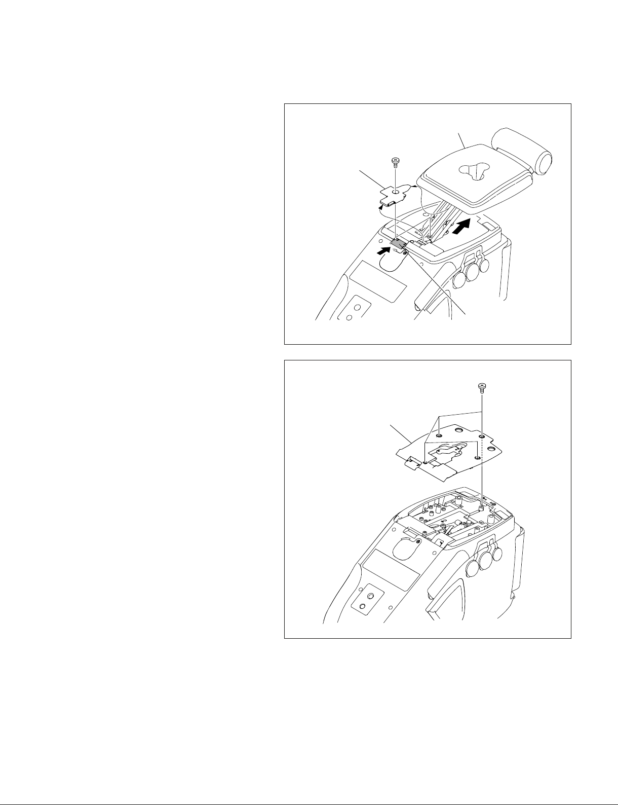
2-2-5. Handle Top Cover Assembly
1. Open the microphone holder assembly.
2. Remove the two screws, and remove the
microphone holder assembly.
B2.6 x 6
Microphone holder
assembly
3. Remove the spring and the four screws, and
remove the accessory shoe.
4. Remove the five screws, and remove the
handle top cover assembly.
5. Reinstall the removed parts by reversing the
steps of removal.
M2 x 6
Accessory
shoe
M2 x 4
Spring
Handle top
cover assembly
PMW-EX3
2-5
Page 32

2-2-6. KSW-54 Board, Control Switch
Block
1. Refer to Section 2-2-5 and remove the
“Handle Top Cover Assembly”.
2. Remove the rubber switch key.
3. Disconnect the HN-349 board from the
connector (CN5).
4. Disconnect the three harnesses from the three
connectors (CN2, CN7 and CN301).
Rubber switch key
KSW-54 board
CN301
CN5
CN7
Harness
CN2
5. Remove the three screws securing the control
switch block.
6. Remove the four screws securing the KSW54 board.
7. Disconnect the harness from the connector
(CN300) on side-B of the KSW-54 board.
8. Disconnect the control switch block from the
connector (CN4) on side-B of the KSW-54
board.
9. Disconnect the HN-328 board from the
connector (CN1) on side-B of the KSW-54
board.
Harness
PSW2 x 5
Control switch block
Harness
PSW2 x 5
M2 x 4
HN-349 board
KSW-54 board
CN4
CN300
CN1
Harness
M2 x 4
HN-328 board
10. Reinstall the removed parts by reversing the
steps of removal.
2-6
PMW-EX3
Page 33

2-2-7. IF-1069 Board, LED-469 Board
1. Refer to Section 2-2-5 and remove the
“Handle Top Cover Assembly”.
2. Disconnect the flexible flat cable from the
connector (CN4) on the IF-1069 board.
n
The life of the flexible board and the flexible
flat cable will be significantly shortened if
they are folded. Be very careful not to fold
them.
3. Disconnect the HN-348 board from the
connector (CN5) on the IF-1069 board.
4. Disconnect the harness from the connector
(CN3) on the IF-1069 board.
5. Remove the two screws, and remove the IF1069 board.
6. Disconnect the three harnesses from the three
connectors (CN1, CN2, CN3) on the LED469 board.
7. Remove the screw, and remove the LED-469
board.
Knob
M2 x 4
IF-1069 board
S1
CN3
Harness
M2 x 4
CN4
CN5
HP-144 board
Flexible flat cable
HN-348 board
LED-469 board
CN1
CN3
M2 x 4
CN2
8. Reinstall the removed parts by reversing the
steps of removal.
n
Check that the switch (S1) on the IF-1069
board engages with the knob.
IF-1069
board
S1
Knob
PMW-EX3
2-7
Page 34

2-2-8. AXM-36 Board, HN-349 Board
1. Refer to Section 2-2-5 and remove the
“Handle Top Cover Assembly”.
2. Remove the rubber switch key.
3. Remove the two screws, and remove the out
microphone bracket.
4. Disconnect the HN-349 board from the
connector (CN5) on the KSW-54 board.
5. Remove the four screws, and remove the
AXM-36 board in the direction of the arrow.
6. Disconnect the HN-349 board from the
connector (CN3) on the AXM-36 board.
icrophone
Out m
bracket
HN-349 board
AXM-36 board
B2.6 x 5
Rubber switch key
CN3
KSW-54 board
7. Reinstall the removed parts by reversing the
steps of removal.
P2.6 x 6
CN5
P2.6 x 6
2-8
PMW-EX3
Page 35

2-2-9. Handle Assembly
1. Refer to Section 2-2-5 and remove the
“Handle Top Cover Assembly”.
2. Remove the two screws, and remove the rear
shoe bracket.
3. Disconnect the harness from the connector
(CN1) on the HP-144 board.
4. Remove the connector cover (HP) and the
two screws, and remove the HP-144 board.
5 Remove the lens from the main unit.
M2 x 4
B2.6 x 6
HP-144 board
CN1
Rear shoe bracket
Lens
Main unit
Connector cover (HP)
6. Disconnect the flexible flat cable from the
connector (CN4) on the IF-1069 board.
n
The life of the flexible board and the flexible
flat cable will be significantly shortened if
they are folded. Be very careful not to fold
them.
7. Disconnect the harness from the connector
(CN2) on the LED-469 board.
8. Remove the two screws, and remove the front
cover handle.
9. Disconnect the connector (CN2) of the HN328 board from the connector (CN800) on the
HN-343 board.
10. Remove the three screws. Lift up the handle
assembly and disconnect the connector on the
DPR-289A board.
LED-469 board
CN2
Coaxial cable
with connector
Flexible flat cable
B2.6 x 6
IF-1069 board
CN4
Handle assembly
B2.6 x 6
HN-343 board
CN800
DPR-289A board
connector
Front cover
handle
M2 x 4
HN-328 board
CN2
11. Reinstall the removed parts by reversing the
steps of removal.
PMW-EX3
2-9
Page 36

2-2-10. Microphone Assembly
1. Refer to Sections 2-2-5, 2-2-6 and 2-2-9, and
remove the “Handle Assembly” removal.
2. Turn the lock lever in the direction of arrow
A, loosen the two screws of a, and remove
the lock lever.
3. Remove the two screws securing the front
bottom cover.
4. While pushing the front bottom cover in the
direction of arrow B paying attention not to
damage the three claws, remove the front
bottom cover in the direction of arrow C.
5. Remove the two screws, and pull out the
microphone assembly in the direction of
arrow D.
Loosen screws of a.
M2 x 4
B
A
Lock lover
M2 x 4
C
Front bottom cover
Claws
M2 x 4
Microphone
assembly
D
6. Reinstall the removed parts by reversing the
steps of removal.
a : Double-point set screw
2-10
PMW-EX3
Page 37

2-2-11. Microphone Unit, MA-164
Board, RM-214 Board
1. Refer to Sections 2-2-5, 2-2-6, 2-2-9 and 2-210, and disassemble the unit up to “Microphone Assembly” removal.
2. Remove the shield sheet.
3. Remove the three screws of a, and remove
the microphone case.
4. Remove the screw of b, and remove the
microphone unit.
Shield sheets
Microphone unit
Microphone case
b
Microphone cover
5. Disconnect the three harnesses from the three
connectors (CN1, CN2, CN3) on the MA-164
board.
6. Remove the two screws of c, and remove
the MA-164 board.
7. Disconnect the harness from the connector
(CN1) on the RM-214 board.
8. Remove the screw of d, and remove the
RM-214 board.
9. Reinstall the removed parts by reversing the
steps of removal.
a : P2 tapping 2 x 5
b : P2 tapping 2 x 5
d
CN1
RM-214
board
Harnesses
c : P2 tapping 2 x 5
d : P2 tapping 2 x 5
CN1
CN3
CN2
c
Microphone unit
Harness
MA-164
Harness
a
board
PMW-EX3
2-11
Page 38

2-2-12. SWC-49 Board
1. Refer to Sections 2-2-5, and 2-2-9, and
disassemble the unit up to “Handle Assembly” removal.
2. Disconnect the HN-348 board from the
connector (CN100) on the SWC-49 board.
3. Remove the two screws, and remove the top
panel cover.
HN-348 board
Top panel cover
SWC-49 board
CN100
M2 x 4
4. Remove the two screws. Remove the top
panel earth bracket, the SWC-49 board and
the key top assembly (top panel).
n
The life of the flexible board and the flexible card
wire will be significantly shortened if they are
folded. Be very careful not to fold them.
5. Reinstall the removed parts by reversing the
steps of removal.
Tapping
2 x 5
Top panel earth bracket
Key top assembly
(top panel)
SWC-49 board
Top panel cover
2-12
PMW-EX3
Page 39

2-2-13. Inside Panel Assembly
1. Refer to Sections from 2-2-1 to 2-2-3, 2-2-5
and 2-2-9, and disassemble the unit up to
“Handle Assembly” removal.
2. Remove the two connector covers from the
connectors.
3. Remove the six screws. Disengage the six
protrusions of the inside panel from the
corresponding six dowels until the inside
panel floats slightly.
n
The inside panel is connected to the AU-318
board via HN-344 board.
4. Disconnect the HN-344 board connector
(CN100) from the AU-318 board connector
(CN4) that is located in the bottom of the
unit.
Protrusion of
inside panel
Dowel
M2 x 4
M2 x 4
Connector
Connector covers
M2 x 4
Inside panel assembly
Inside panel
assembly
HN-344 board
CN100
AU-318 board
CN4
5. Remove the inside panel assembly slightly in
the direction of arrow A.
6. Disconnect the six connectors and remove
them through the six holes, and remove the
inside panel assembly in the direction of
arrow B.
7. Disconnect the connector (CN2) of the HN337 board from the connector (CN101) of the
ASW-66 board, and remove the inside panel
assembly.
Holes of inside panel assembly
Connectors
HN-337 board
CN2
B
ASW-66 board
CN101
8 Reinstall the removed parts by reversing the
steps of removal.
PMW-EX3
A
Inside panel assembly
2-13
Page 40

2-2-14. CN-3050 Board
1. Refer to Sections from 2-2-1 to 2-2-3, 2-2-5,
2-2-9 and 2-2-13, and disassemble the unit up
to “Inside Panel Assembly” removal.
2. Disconnect the harness from the connector
(CN1) on the CN-3050 board.
3. Remove the two screws, and remove the CN3050 board.
4. Reinstall the removed parts by reversing the
steps of removal.
CN-3050 board
Tapping
2 x 5
CN1
2-14
PMW-EX3
Page 41

2-2-15. Connector Rear Assembly
1. Refer to Sections from 2-2-1 to 2-2-3, 2-2-5,
2-2-9 and 2-2-13, and disassemble the unit up
to “Inside Panel Assembly” removal.
2. Disconnect the power supply harness from
the connector (CN2) on the RE-260 board.
3. Remove the four screws, and remove the
connector rear assembly.
4. Disconnect the harness from the connector
(CN6) on the CN-3024 board.
5. Disconnect the harness from the connector
(CN1) on the CN-3050 board.
6. Disconnect the coaxial cable assembly from
the coaxial connector, and remove the
connector rear assembly.
Connector rear assembly
Coaxial cable
assembly
Screws
B2.6 x 6
Coaxial connector
7. Reinstall the removed parts by reversing the
steps of removal.
RE-260 board
CN2
CN-3050 board
CN1
CN-3024 board
CN6
Power supply harness
PMW-EX3
2-15
Page 42

2-2-16. ASW-66 Board, SW-1412
Board
1. Refer to Sections from 2-2-1 to 2-2-3, 2-2-5,
2-2-9 and 2-2-13, and disassemble the unit up
to “Inside Panel Assembly” removal.
2. Disconnect the connectors and the AU
volume block from the three connectors
(CN100, CN102, CN103) on the ASW-66
board.
3. Release the harness from the two claws of the
inside panel assembly. (Refer to Fig. 2.)
4. Remove the four screws, and remove the
ASW-66 board in the direction of the arrow.
(Refer to Fig. 1.)
5. Remove two pieces of the AU slide switch
(1) and two pieces of the AU slide switch (2)
of the ASW-66 board from the corresponding
AU slide levers. (Refer to Fig. 1.)
n
Be careful not drop the AU slide switches so
as not to lose them.
AU slide switch guide
AU slide switches (2)
S101
S103
AU slide switches (1)
AU slide switch lever
S100
S102
ASW-66 board
Harness
Claws of inside
panel assembly
ASW-66 board
SW-1412 board
(Fig. 2)
6. Remove the AU slide switch guide from the
ASW-66 board.
7. Disconnect the harness from the connector
(CN100) on the SW-1412 board.
8. Remove the two screws, and remove the SW1412 board.
m
. The life of the flexible board and flexible card
wire will be significantly shortened if they are
folded. Be very careful not to fold them.
. Be careful not to make mistake the AU slide
switch (1) for the AU slide switch (2) because
they are different in size.
9. Reinstall the removed parts by reversing the
steps of removal.
n
Check that the four knobs of the AU slide
switch are normally engaged with the four
corresponding switches (S100 through S103)
on the ASW-66 board.
Knob of AU slide switch (Fig. 1)
CN103
ASW-66 board
Tapping
2 x 5
CN102
CN100
Tapping
2 x 5
SW-1412 board
Inside panel assembly
CN100
AU volume block
2-16
PMW-EX3
Page 43

2-2-17. SW-1410 Board
1. Refer to Sections from 2-2-1 to 2-2-3, 2-2-5,
2-2-9 and 2-2-13, and disassemble the unit up
to “Inside Panel Assembly” removal.
2. Disconnect the SWC-48 board from the
connector (CN300) on the SW-1410 board.
3. Remove the three screws, and remove the
SW-1410 board.
4. Remove the power switch from the power
switch lever of the SW-1410 board.
5. Remove the power switch slide rail from the
SW-1410 board.
n
Be careful not to drop and lose the power switch.
Inside panel assembly
CN300
SW-1410 board
Tapping
2 x 5
SWC-48 board
6. Reinstall the removed parts by reversing the
steps of removal.
n
Check that the knob of the power switch is
normally engaged with the switch (S301) on
the SW-1410 board.
Power switch
S301
Power switch slide rail
SW-1410 board
Power switch lever
S301
Knob of power switch
PMW-EX3
2-17
Page 44

2-2-18. HN-344 Board
1. Refer to Sections from 2-2-1 to 2-2-3, 2-2-5,
2-2-9 and 2-2-13, and disassemble the unit up
to “Inside Panel Assembly” removal.
2. Disconnect the SWC-48 board from the
connector (CN300) on the SW-1410 board.
3. Remove the four screws, and remove the
inside panel assembly (1).
4. Disengage the two claws, and remove the CN
holder.
5. Disconnect the HN-344 board connector
(CN101) from the SWC-48 board connector
(CN100).
SW-1410 board
CN300
Inside panel assembly (1)
Tapping
2 x 5
SWC-48 board
SWC-48 board
CN100
HN-344 board
CN101
Inside panel assembly (2)
CN holder
Claws
6. Reinstall the removed parts by reversing the
steps of removal.
2-18
PMW-EX3
Page 45

2-2-19. HN-343 Board, SWC-48 Board
1. Refer to Sections from 2-2-1 to 2-2-3, 2-2-5,
2-2-9, 2-2-13 and 2-2-18, and disassemble
the unit up to “HN-344 Board” removal.
2. Remove the two screws of a, and disconnect the HN-343 board from the connector
(CN700) on the SWC-48 board.
3. Remove the tape (SWC48) from the HN-343
board.
4. Disconnect the harness from the connector
(CN600) on the SWC-48 board. Remove the
harness from the bracket (frame/full auto
bracket) in the direction of the arrow.
5. Remove the six screws of b, and remove the
SWC-48 board.
Inside panel assembly (1)
Bracket
(Frame/full auto bracket)
Harness
HN-343 board
CN700
n
The life of the flexible board and flexible card
wire will be significantly shortened if they are
folded. Be very careful not to fold them.
M2 x 4
Inside panel assembly (1)
Screws b
b
Tape (SWC48)
M2 x 4
a
CN600
SWC-48 board
b
Tapping
2 x 5
PMW-EX3
2-19
Page 46

6. Remove the top key (frame) and the light
interception cushion from the SWC-48 board.
7. Remove the tape (SWC48) from the SWC-48
board.
8. Remove the three screws, and remove the
SWC-48 board from the bracket (frame/full
auto bracket).
9. Reinstall the removed parts by reversing the
steps of removal.
Light interception
cushion
Top key
(frame)
M2 x 4
SWC-48 board
P2 x 4
Bracket
(Frame/full auto bracket)
Bracket
(Frame/full auto bracket)
Tape
(SWC48)
SWC-48 board
Volume
n
The life of the flexible board and flexible card
wire will be significantly shortened if they are
folded. Be very careful not to fold them.
Hole of
SWC-48 board
Fold
SWC-48 board
2-20
PMW-EX3
Page 47

2-2-20. SW-1411 Board
1. Refer to Sections from 2-2-1 to 2-2-3, 2-2-5,
2-2-9, 2-2-13, 2-2-18 and 2-2-19, and
disassemble the unit up to “SWC-48 Board”
removal.
2. Disconnect the harness from the connector
(CN400) on the SW-1411 board.
3. Remove the four screws, and remove the
SW-1411 board.
4. Remove the two light interception spacers
from the inside panel assembly (1).
5. Reinstall the removed parts by reversing the
steps of removal.
2-2-21. Outside Panel Sub Assembly
Harness
Tapping
2 x 5
Inside panel assembly (1)
Light interception
spacers
CN400
SW-1411 board
1. Refer to Sections from 2-2-1 to 2-2-3, 2-2-5
and 2-2-9, and disassemble the unit up to
“Handle Assembly” removal.
2. Remove the six screws. Disengage the six
protrusions of the outside panel sub assembly
from the corresponding six dowels, and
remove the outside panel sub assembly in the
direction of the arrow.
3. Reinstall the removed parts by reversing the
steps of removal.
n
When installing the outside panel sub
assembly (to be abbreviated as “O-assembly”
hereafter), stand the unit and the O-assembly
vertically. Then, move the O-assembly
toward the unit in parallel with the unit, and
install the O-assembly.
Do not install the O-assembly at an angle.
Main unit
M2 x 4
Outside panel sub
assembly
Protrusion of outside
panel sub assembly
M2 x 4
Dowel
PMW-EX3
2-21
Page 48

2-2-22. SW-1389 Board
1. Refer to Sections from 2-2-1 to 2-2-3, 2-2-5,
2-2-9, 2-2-13 and 2-2-21, and disassemble
the unit up to “Outside Panel Sub Assembly”
removal.
2. Disengage the claw and the two dowels of the
front panel from the SW board bracket.
3. Disconnect the HN-345 board from the
connector (CN2) on the AU-318 board.
4. Remove the two screws, and remove the SW1389 board.
5. Disconnect the HN-345 board from the
connector (CN500) on the SW-1389 board.
Claw of SW board bracket
SW-1389 board
M2 x 4
Front panel assembly
Claws
CN500
AU-318 board
CN2
HN-345 board
SHUTTER ON/OFF knob
6. Reinstall the removed parts by reversing the
steps of removal.
n
Check that the SHUTTER ON/OFF knob is
normally engaged with the switch (S502) on
the SW-1389 board.
S502
2-22
PMW-EX3
Page 49

2-2-23. Battery Case Assembly
1. Refer to Sections from 2-2-1 to 2-2-3, 2-2-5,
2-2-9, 2-2-13 and 2-2-21, and disassemble
the unit up to “Outside Panel Sub Assembly”
removal.
2. Disconnect the power supply harness from
the connector (CN2) on the RE-260 board.
3. Remove the power supply harness from
groove of the main frame.
4. Remove the four screws of the battery case
assembly.
5. Disconnect the power supply harness through
clearance between the main frame and the
connector rear assembly, and remove the
battery case assembly.
Connector rear assembly
RE-260 board
CN2
Screws
Battery case assembly
M2 x 4
Power supply harness
Main frame
Groove of main frame
6. Reinstall the removed parts by reversing the
steps of removal.
Power supply harness
PMW-EX3
2-23
Page 50

2-2-24. EX-DD Assembly
1. Refer to Sections from 2-2-1 to 2-2-3, 2-2-5,
2-2-9, 2-2-13 and 2-2-21, and disassemble
the unit up to “Outside Panel Sub Assembly”
removal.
2. Disconnect the CN-3022 board connector
(CN1) and the CN-3023 board connector
(CN1) from the two connectors on the DPR289A board.
3. Disconnect the three harnesses from the two
connectors (CN1) on the two EC-63 boards
and one connector (CN1) on the RE-260
board respectively.
DPR-289A board
connectors
CN-3022 board
CN1
Coaxial cable
with connectors
RE-260 board
CN1
CN-3023 board
CN1
EC-63 boards
CN1
n
The coaxial cable with connector uses the fine
pitch coaxial cable. Be careful when arranging it.
When disconnecting the coaxial cable with
connector, never remove it by pulling the cable.
Be sure to hold the connector to remove.
Contaction
surface
OK
Remove by holding
the connector.
Polarity marks
NG
Do not pull the cable.
2-24
PMW-EX3
Page 51

4. Place the unit with its inside (left side)
facing toward you. Disconnect the power
supply harness from the connector (CN2) of
the RE-260 board. (Disconnect the power
supply harness in the direction of arrow A
from the groove of the main frame.)
5. Remove the two screws. Push the CN-3022
board and the CN-3023 board in the direction of arrow B, and remove the EX-DD
assembly in the direction of arrow C.
n
The life of the flexible board and flexible card
wire will be significantly shortened they are
folded. Be very careful not to fold them.
Groove of main frame
A
Power supply harness
C
M2 x 4
6. Reinstall the removed parts by reversing the
steps of removal.
EX-DD assembly
RE-260 board
CN2
CN-3022 board
B
EX-DD assembly
CN-3023 board
PMW-EX3
2-25
Page 52

2-2-25. CN-3023 Board
1. Refer to Sections from 2-2-1 to 2-2-3, 2-2-5,
2-2-9, 2-2-13, 2-2-21 and 2-2-24, and
disassemble the unit up to “EX-DD Assembly” removal.
2. Remove the four screws securing the RE-261
board.
3. Disconnect the RE-261 board connector
(CN2) from the RE-260 board connector
(CN201), and remove the RE-261 board in
the direction of the arrow.
4. Disconnect the CN-3023 board connector
(CN2) from the RE-261 board connector
(CN1), and remove the CN-3023 board.
5. Remove the cushion CN3007 from the CN3023 board.
6. Reinstall the removed parts by reversing the
steps of removal.
CN-3023 board
CN2
RE-260 board
CN1
M2 x 4
RE-261 board
CN2
Cushion
CN3007
CN201
2-2-26. RE-260 Board
1. Refer to Sections from 2-2-1 to 2-2-3, 2-2-5,
2-2-9, 2-2-13, 2-2-21, 2-2-24 and 2-2-25, and
disassemble the unit up to “CN3023 Board”
removal.
2. Remove the four screws, and lift up the RE260 board in the direction of arrow A.
3. Disconnect the CN-3022 board connector
(CN2) from the RE-260 board connector
(CN200) in the direction of arrow B, and
remove the CN-3022 board.
4. Remove the RE-260 board from the EX-DD
bracket in the direction of arrow C.
RE-260 board
A
CN2
CN-3022 board
CN2
CN-3022 board
EX-DD bracket
C
CN200
B
M2 x 4
CN200
RE-260 board
5. Reinstall the removed parts by reversing the
steps of removal.
2-26
PMW-EX3
Page 53

2-2-27. EC-63 Board
1. Refer to Sections from 2-2-1 to 2-2-3, 2-2-5,
2-2-9, 2-2-13, 2-2-21 and from 2-2-24 to 2-226, and disassemble the unit up to “RE-260
Board” removal.
2. Remove the two screws, and remove the EXDD bracket in the direction of arrow A.
3. Remove the four screws, and remove the EC63 board.
4. Remove the heat sink (EC) rear.
5. Remove the three screws, disengage protrusion of the heat sink (EX) rear from the
groove, and remove the heat sink (EX) rear in
the direction of arrow B.
6. Remove the radiation sheet from the EC-63
board.
7. Remove the screw, and remove the EC-63
board.
M2 x 4
EC-63 board
M2 x 4
EX-DD bracket
EX-DD bracket
Heat sink
(EX) front
Heat sink
(EX) rear
protrusion
Notch
A
B
8. Reinstall the removed parts by reversing the
steps of removal.
PMW-EX3
Radiation sheet
(EC) rear
Heat sink
(EX) front
M2 x 4
Heat sink (EX) rear
Radiation sheet
M2 x 4
EC-63 board
EX bracket
2-27
Page 54

2-2-28. PS-747 Board
1. Refer to Sections from 2-2-1 to 2-2-3, 2-2-5,
2-2-9, 2-2-13, 2-2-21 and 2-2-24, and
disassemble the unit up to “EX-DD Assembly” removal.
2. Place the unit with the lens facing downward.
3. Disconnect the harness from the connector
(CN1) on the PS-747 board.
4. Loosen the three screws, and slide the outside
connector assembly slightly in the direction
of arrow A.
n
Only loosen the three screws and do not
remove them.
(These three screws are removed when
removing the outside connector assembly in
Section 2-2-30.)
Claws of capacitor case
B
M2 x 4
PS-747 board
CN1
A
5. Remove one screw and disengage the two
claws of the capacitor case in the direction of
arrow B.
6. Remove the PS-747 board from the capacitor
case.
7. Reinstall the removed parts by reversing the
steps of removal.
n
When installing the outside connector
assembly, tighten finally the three screws
securing the outside connector assembly at
this step.
Loosen
screws.
PS-747 board
Capacitor case
Outside connector
assembly
2-28
PMW-EX3
Page 55

2-2-29. TX-129 Board
1.
Refer to Sections from 2-2-1 to 2-2-3, 2-2-5, 2-29, 2-2-13, 2-2-21, 2-2-24 and 2-2-28, and disassemble the unit up to “PS-747 Board” removal.
2. Disconnect the harness from the connector
(CN3) on the HN-337 board.
3. Disconnect the coaxial cable from the coaxial
cable connector on the TX-129 board.
4. Loosen the three screws, and slide the outside
connector assembly slightly in the direction
of arrow A.
n
Only loosen the three screws and do not
remove them.
(These three screws are removed when
removing the outside connector assembly in
Section 2-2-30.)
5. Remove the three screws, disengage protrusion of the pad rail and the two dowels from
groove of the main frame, and remove the
pad rail in the direction of arrow B.
Groove of main frame
Tapping
BTB2.6 x 6
Loosen screws.
Outside connector
assembly
Pad rail
A
Coaxial cable assembly
TX-129 board
coaxial cable
connector
HN-337 board
CN3
Protrusion of pad rail
Dowels
B
6. Remove the tape 50 and the tape 60 from the
TX block.
7. Disconnect the four harnesses from the four
connectors (CN100, CN700, CN800, CN901)
on the TX-129 board.
8. Remove the three screws, remove the TX
block from the two dowels, and remove the
TX block in the direction of the arrow.
m
. When pulling out the TX block in the direction
of the arrow, be very careful not to cut the
harnesses resulting open circuit and not to
entangle the harnesses.
. The coaxial cable with connector uses the fine
pitch coaxial cable. Be careful when arranging
it. When disconnecting the coaxial cable with
connector, never remove it by pulling the cable.
Be sure to hold the connector to remove.
M2 x 4
CN700
CN800
TX-129 board
TX block
Tape 50
Tape 60
CN100
TX block
Dowels
Coaxial cable
with connectors
PMW-EX3
TX-129 board
CN901
2-29
Page 56

9. Remove the four screws, and remove the heat
sink.
10. Remove the DPR-TX bracket assembly and
the radiation sheet (TX) from the TX-129
board.
11. Reinstall the removed parts by reversing the
steps of removal.
M2 x 4
Heat sink
Radiation sheet (TX)
TX-129 board
DPR-TX
bracket assembly
2-2-30. Outside Connector Assembly
1. Refer to Sections from 2-2-1 to 2-2-3, 2-2-5,
2-2-9, 2-2-13, 2-2-21, 2-2-24, 2-2-28 and 22-29, and disassemble the unit up to “TX
Block” removal.
2. Disconnect the HN-337 board connector
(CN1) from the DPR-289A board connector
b, and remove the HN-337 board.
3. Disconnect the HN-347 board connector
(CN1) from the DPR-289A board connector
a.
4. Remove the three screws, and remove the
outside connector assembly.
5. Disconnect the harness (DC146-RE260) from
the connector (CN1) on the DC-146 board.
6. Reinstall the removed parts by reversing the
steps of removal.
m
. The life of the flexible board and the flexible
card wire will be significantly shortened if they
are folded. Be very careful not to fold them.
. When installing the outside connector assem-
bly, tighten the three screws tentatively.
Tighten them finally when installing the PS-747
board in section 2-2-28.
2-30
HN-337 board
B2.6 x 6
Outside connector
assembly
HN-347 board
CN1
DPR-289A board
CN1
DC-146 board
CN1
Connector b
Connector a
Harness (DC146-RE260)
PMW-EX3
Page 57

2-2-31. DPR-289A Board
1. Refer to Sections from 2-2-1 to 2-2-3, 2-2-5,
2-2-9, 2-2-13, 2-2-21, 2-2-24, and from 2-228 to 2-2-30, and disassemble the unit up to
“Outside Connector Assembly” removal.
2. Disconnect the HN-326 board connector
(CN1) from the DPR-289A board connector
c.
3. Disconnect the three prism connectors a, b
and d from the corresponding three connectors A, B and D on the DPR-289A board.
4. Disconnect the five harnesses and the flexible
flat cable from the corresponding six connectors E, F, G, H, I and J on the DPR289A board.
5. Remove the screw, disengage the DPR-289A
board from the two dowels, and remove the
DPR-289A board in the direction of the
arrow.
m
. The coaxial cable with connector uses the fine
pitch coaxial cable. Be careful when arranging
it. When disconnecting the coaxial cable with
connector, never remove it by pulling the cable.
Be sure to hold the connector to remove.
. The life of the flexible board and the flexible
card wire will be significantly shortened if they
are folded. Be very careful not to fold them.
M2 x 4
DPR-289A
board
C
D
B
A
E
F
Coaxial cable
with connectors
DPR-289A
board
Harness
J
G
HN-326 board
CN1
Coaxial cable
with connectors
I
H
Radiation
sheets
Prism connectors
d
b
c
a
Flexible flat cable
Dowels
6. Remove the three radiation sheets from the
DPR-289A board.
7. Reinstall the removed parts by reversing the
steps of removal.
n
When connecting the coaxial cable with
connector, be careful of the following points:
. Do not insert the connector at a slant angle.
. Check to see that the contacting surface is
free from stain and dust.
. Hold the connector with its contacting
surface facing upward, and check that the
polarity marks are aligned.
PMW-EX3
Contacting
surface
OK
Insert the cable by holding
the connector.
Polarity marks
NG
Do not bend the cable.
2-31
Page 58

2-2-32. Lens Mount Block
1. Refer to Sections from 2-2-1 to 2-2-3, 2-2-5,
2-2-9, 2-2-13, 2-2-21, 2-2-24, and from 2-228 to 2-2-31, and disassemble the unit up to
“DPR-289A Board” removal.
2. Disconnect the harness from the connector
(CN7) on the AU-318 board.
3. Remove the four screws, disengage the main
frame block from the two dowels, and
remove the main frame block.
4. When removing the main frame block,
remove the three prism connectors and the
HN-326 board in the direction of the arrow,
and remove the lens mount block.
Main frame block
Prism
connectors
B2.6 x 6
AU-318 board
CN7
n
The life of the flexible board and the flexible card
wire will be significantly shortened if they are
folded. Be very careful not to fold them.
5. Reinstall the removed parts by reversing the
steps of removal.
2-2-33. Prism Block Unit
1. Refer to Sections from 2-2-1 to 2-2-3, 2-2-5,
2-2-9, 2-2-13, 2-2-21, 2-2-24, and from 2-228 to 2-2-32, and disassemble the unit up to
“Lens Mount Block” removal.
2. Remove the four screws, and remove the
prism block unit.
n
The life of the flexible board and the flexible card
wire will be significantly shortened if they are
folded. Be very careful not to fold them.
HN-326 board
Lens mount block
Dowels
B2.6 x 6
M2 x 5
Prism block
unit
3. Reinstall the removed parts by reversing the
steps of removal.
2-32
Lens mount block
PMW-EX3
Page 59

2-2-34. SE-923 Board
1. Refer to Sections from 2-2-1 to 2-2-3, 2-2-5,
2-2-9, 2-2-13, 2-2-21, 2-2-24, and from 2-228 to 2-2-32, and disassemble the unit up to
“Lens Mount Block” removal.
2. Disconnect the SE-923 board from the
connector (CN102) on the IR-42 board.
3. Remove the two screws, disengage the SE923 board from the two dowels, and remove
the SE-923 board.
M2 x 4
SE-923 board
n
The life of the flexible board and the flexible card
wire will be significantly shortened if they are
folded. Be very careful not to fold them.
4. Reinstall the removed parts by reversing the
steps of removal.
n
When installing the SE-923 board, place the filter
sheet underneath the SE-923 board, and install the
SE-923 board.
Lens mount block
IR-42 board
CN102
Dowels
Filter sheet
PMW-EX3
2-33
Page 60

2-2-35. AU-318 Board
1. Refer to Sections from 2-2-1 to 2-2-3, 2-2-5,
2-2-9, 2-2-13, 2-2-21, 2-2-24, and from 2-228 to 2-2-32, and disassemble the unit up to
“Lens Mount Block” removal.
2. Pull the three prism connectors in the direction of arrow A, and remove the HN-345
board and the HN-346 from the two connectors (CN1, CN2) on the AU-318 board.
3. Remove the two screws, and remove the AU318 board from the two grooves of the front
frame in the direction of arrow B.
4. Disconnect the HN-326 board connector
(CN2) from the connector (CN6) on the AU318 board, and remove the AU-318 board.
5. Remove the cushion (front) from the HN-326
board.
m
. The life of the flexible board and the flexible
card wire will be significantly shortened if they
are folded. Be very careful not to fold them.
. Be careful not to drop the inside PC board
guide.
HN-326 board
CN6
M2 x 4
AU-318 board
Prism connectors
Groove of front frames
B
AU-318 board
Groove of front frames
CN2
CN1
CN2
Lens mount block
Cushion (front)
HN-346 board
HN-345 board
A
Inside PC board guide
6. Reinstall the removed parts by reversing the
steps of removal.
2-34
PMW-EX3
Page 61

2-2-36. IR-42 Board
1. Refer to Sections from 2-2-1 to 2-2-3, 2-2-5,
2-2-9, 2-2-13, 2-2-21, 2-2-24, and from 2-228 to 2-2-33, and disassemble the unit up to
“AU-318 Board” removal.
2. Disconnect the SE-923 board and the HN346 board from the two connectors (CN102,
CN103) on the IR-42 board.
3. Remove the screw, and remove the IR-42
board.
4. Remove soldering at 14 points of the IR-42
board.
5. Remove the four screws, and remove the two
mount (C) connectors.w
n
The life of the flexible board and the flexible card
wire will be significantly shortened if they are
folded. Be very careful not to fold them.
HN-346 board
CN102
Remove soldering from the
Fourteen points.
SE-923 board
Lens mount block
CN103
M2 x 4
IR-42 board
6. Reinstall the removed parts by reversing the
steps of removal.
Mount (C) connectors
K1.7 x 5
(Precision)
PMW-EX3
2-35
Page 62

2-2-37. Replacing the Parts in the
Lens Grip
Removing the grip cover
1. Remove the three screws a, and remove the
screw b. (Fig. 1)
2. While pressing the RELEASE button, press
the T side of the T/W zoom switch, and rotate
the grip cover in the direction of the arrow,
then remove the grip cover. (Fig. 2)
3. Disconnect the harness from the connector of
the T/W zoom switch. (Fig. 3)
Replacing the cap (START/STOP)
1. Remove the cap (START/STOP) by pushing
it in from the outside of the grip cover. (Fig.
5)
2. Install the new cap (START/STOP) by
aligning its notch with the protrusion of the
grip cover. (Fig. 5)
Replacing the rear cover and the grip belt
1. Disengage the two claws from the inside of
the grip cover, and remove the rear cover.
(Fig. 4)
2. Separate the grip belt from the buckle, and
pull it off from the grip cover. (Fig. 6)
3. Install the new grip belt by reversing the
steps of removal. (Fig. 6)
4. Engage the rear cover with the grip cover.
a
a
T/W zoom switch
Fig.1
Fig.3
a
T/W zoom switch
Claws
b
Grip cover
RELEASE
button
Harness
T sideW side
Fig.2
Grip cover
Installing the grip cover
1. Connect the harness to the connector of the
T/W zoom switch. (Fig. 3)
2. Align the hole of the grip cover with the
RELEASE button. While pressing the T side
of the T/W zoom switch, assemble it by
rotating it in the direction opposite to the
arrow. (Fig. 2)
3. Install the three screws a, and the screw b.
(Fig. 1)
2-36
Grip cover (inside)
Cap
(START/STOP)
Notch
Fig.5
Grip cover
(Inside)
Rear cover
Fig.4
Protrusion
Buckle
Grip belt
Fig.6
PMW-EX3
Page 63

Section 3
SERVICE Menu
3-1. SERVICE Menu List
1. MAINTENANCE menu list
Menu Item Submenu Item Choice Function
Test Saw _ On Turns On or Off the Test Saw.
Off
Auto BLK _ Execute Starts up the auto black balance adjustment.
Balance Cancel
Black Shading Setting On Turns On or Off the black shading correction.
Channel Sel G Selects the channel (R-ch or G-ch or B-ch) to
H Saw _99 to +99 Adjusts the black shading H Saw correction level.
H Para _99 to +99 Adjusts the black shading H Para correction level.
V Saw _99 to +99 Adjusts the black shading V Saw correction level.
V Para _99 to +99 Adjusts the black shading V Para correction level.
Auto BLK Shad Execute Starts up the auto black shading correction.
White Shading Setting On Turns On or Off the white shading correction.
Channel Sel G Selects the channel (R-ch or G-ch or B-ch) to
H Saw _99 to +99 Adjusts the white shading H Saw correction level.
H Para _99 to +99 Adjusts the white shading H Para correction level.
V Saw _99 to +99 Adjusts the white shading V Saw correction level.
V Para _99 to +99 Adjusts the white shading V Para correction level.
Flare G Flare _99 to +99 Adjusts the G-ch flare correction level.
B Flare _99 to +99 Adjusts the B-ch flare correction level.
R Flare _99 to +99 Adjusts the R-ch flare correction level.
Off
B execute black shading adjustment on.
R (The present setup values of H Saw, H Para, V
Saw and V Para for the selected channel are
displayed automatically.)
Cancel
Off
B execute white shading adjustment on. (The
R present setup values of H Saw, H Para, V Saw
and V Para of the selected channel are displayed
automatically.)
2. RPN CORRECT menu list
Menu Item Submenu Item Choice Function
Auto Detection _ Execute Starts up auto RPN.
Cancel
Correction Mode _ Concealment Selects the RPN correction mode that is used to
Compensation register or delete the manual registration.
Channel _ G Selects and displays the channel (R-ch or G-ch or
B B-ch) to execute manual registration or detection
R of RPN correction on.
Cursor _ On Turns On or Off the RPN correction point indicator
Off cursor.
PMW-EX3
3-1
Page 64

Menu Item Submenu Item Choice Function
Cursor H Position _ 1 to 1920 Displays and move the horizontal address of the
Cursor V Position _ 1 to 1080 Displays and move the vertical address of the RPN
Cursor Next __ Moves the RPN correction point indicator cursor
Cursor Prev __ Moves the RPN correction point indicator cursor
Compensation _ 0 to 255 Indicates the RPN compensation level.
Level
Recode _ Execute Registers the RPN.
Cancel
Delete _ Execute Deletes the RPN.
Cancel
Readout Mode _ Field Selects the CMOS readout mode.
Frame
Reset _ Execute Deletes all the RPN that are registered after
Cancel shipment from the factory.
RPN correction point indicator cursor.
correction point indicator cursor.
to the next RPN point.
to the previous RPN point.
3. INFORMATION menu list
Menu Item Submenu Item Choice Function
Serial Number __ Displays the serial number.
Version __ Displays the software version number.
Self Diag Diag Type Type1 Selects the self-diagnostic type.
Item1 Execute Executes self-diagnostic Item 1.
Item2 Execute Executes self-diagnostic Item 2.
Item3 Execute Executes self-diagnostic Item 3.
Item4 Execute Executes self-diagnostic Item 4.
Item5 Execute Executes self-diagnostic Item 5.
Item6 Execute Executes self-diagnostic Item 6.
Item7 Execute Executes self-diagnostic Item 7.
Item8 Execute Executes self-diagnostic Item 8.
Item9 Execute Executes self-diagnostic Item 9.
Item10 Execute Executes self-diagnostic Item 10.
Item11 Execute Executes self-diagnostic Item 11.
Item12 Execute Executes self-diagnostic Item 12.
Item13 Execute Executes self-diagnostic Item 13.
Log Dump _ Execute Records the error log to media.
Type2
Cancel
Cancel
Cancel
Cancel
Cancel
Cancel
Cancel
Cancel
Cancel
Cancel
Cancel
Cancel
Cancel
Cancel
3-2
PMW-EX3
Page 65

3-2. SERVICE Menu Description
3-2-3. Displaying the SERVICE Menu
3-2-1. Basic Menu Operations
Basic Menu Operation
Press the MENU button to enter the menu mode.
Press the PICTURE PROFILE button, the MENU button,
or the STATUS button while the menu is displayed to
close the menu display. The menu display is closed when
the power is turned off.
1. Press the MENU button.
The system enters the menu mode.
For displaying the SERVICE menu, refer to section 32-3 of this manual.
2. Press the arrow key to move the cursor to the desired
setting item and press the SEL/SET button.
Exiting the Menu Mode
Press the MENU button again.
The system exits the menu mode to return to the normal
camera mode.
3-2-2. SERVICE Menu Structure
The SERVICE menu consists of the three SERVICE
dedicated menus and the six ordinary SETUP menus for a
total of nine menus.
SERVICE menu types
Menu name Description
MAINTENANCE Adjustment of parameters
RPN CORRECT Operations regarding the RPN correction
INFORMATION Information display on the particular
PMW-EX3 and self-diagnostics.
The MAINTENANCE menu and the RPN CORRECT
menu can be operated in the CAMERA mode only.
. To display the SERVICE menu, press the CANCEL
button, the MENU button, and the JOG dial at the same
time.
Pressing the MENU button again closes the SERVICE
menu display.
. Once the SERVICE menu has been displayed, simply
pressing the MENU button displays the SERVICE menu
instead of the normal SETUP menu unless the power is
turned off.
3-3. SERVICE Menu Description
3-3-1. MAINTENANCE Menu
The MAINTENANCE menu enables setting for image
device and setting parameters that must be set uniquely to
each PMW-EX3 for correction of non-uniformity between
the respective lens characteristics.
1. Test Saw setting
. Test Saw setting enables the operator to select the Test
Saw signal instead of the imager output signal when
recording or outputting images in CAMERA mode.
2. Executing Auto Black Balance
. Executing the Auto Black Balance triggers the auto
black balance adjustment (automatic black level adjustment).
. When the Auto Black Balance menu is selected, the
Execute and Cancel choices appear.
Selecting Execute starts Auto Black Balance.
. When the Auto Black Balance is executed, the execute
RPN automatic detection.
n
Auto Black Balance cannot be executed from the SERVICE menu under the following settings.
Change the settings to execute Auto Black Balance.
. When Video Format other than HQ 1080/60i or HQ
1080/50i is selected.
. When electronic shutter is operating in the SLS mode.
. When the EX Slow Shutter is set to ON.
PMW-EX3
3-3
Page 66

3. Black Shading Adjustment
Black shading adjustment method
n
All of the Black Shading correction values have been set to
± 0 when shipped from the factory.
(When the Black Shading correction is executed, it results
in height difference of black level at the boundary areas
between the corrected areas). Do not change the Black
Shading correction values to any values other than ± 0
unless it is necessary.
. The Black Shading menu enables the H Saw correction
level adjustment, V Saw correction level adjustment and
parabola correction level adjustment.
. The Black Shading setting menu can be used to turn
Black Shading correction On or Off.
The Black Shading setting is turned On automatically
when the power is turned On.
. The Channel Select menu enables selection of the
channel (G-ch or B-ch or R-ch) to execute the H Saw, H
Para, V Saw, and V Para black shading adjustments on.
. When the Channel Select menu selects any other chan-
nel, the displays of the H Saw, H Para, V Saw, and V
Para setup values are changed to the current setup values
of the channel selected by the Channel Select menu. The
changes are reflected on the H Saw, H Para, V Saw, and
V Para setup values.
. The H Saw menu enables the horizontal Saw black
shading correction (linear increase and decrease) level.
. The H Para menu enables the horizontal Parabola black
shading correction (black level correction at the horizontal center with respect to both ends) level.
. The V Saw menu enables the vertical Saw black shading
correction (linear increase and decrease) level.
. The V Para menu enables the vertical Parabola black
shading correction (black level correction at the vertical
center with respect to both ends) level.
. The Auto BLK Shad menu enables the auto black
shading correction (automatic optimization of the
respective correction values of the black shading correction).
. When Auto BLK Shad menu is selected, the Execute and
Cancel choices appear.
Selecting Execute starts Auto Black Shading.
Preparation
. Connect an HD waveform monitor to the SDI OUT
terminal.
. HD waveform monitor setting: RGB mode
. Lens iris → CLOSE
Adjustment Procedure
. Adjust GAIN and BLK level for easy viewing to ob-
serve.
. Adjust H Saw, H Para, V Saw and V Para for the
respective channels of G-ch, B-ch and R-ch until waveform on the waveform monitor becomes flat.
(H SAW)
(H PARA)
(V SAW) (V PARA)
3-4
PMW-EX3
Page 67

4. White Shading Adjustment
(H SAW)
(H PARA)
(V SAW) (V PARA)
White shading adjustment method
The White Shading menu enables the adjustment of the
horizontal and vertical Saw correction level and parabola
correction level.
m
. The White Shading adjustment cannot be executed for
the correct adjustment values if the object pattern has
non-uniformity or if other conditions such as lens iris
setting and zoom setting are not correctly satisfied. .
. Use a full white pattern for the White Shading adjust-
ment having uniform brightness over the entire area.
. If a full white pattern having uniform brightness over the
entire area is not available, do not execute the G-channel
White Balance adjustment. Instead of it, execute the
White Balance adjustment in the way of aligning the Rchannel waveform and the B-channel waveform to the
waveform of G-channel.
. The White Shading setting menu can be used to turn
White Shading correction On or Off.
The White Shading setting is turned On automatically
when the power is turned On.
. The Channel Select menu enables selection of the
channel (G-ch or B-ch or R-ch) to execute the H Saw, H
Para, V Saw, and V Para white shading adjustments on.
. When the Channel Select menu selects any other chan-
nel, the displays of the H Saw, H Para, V Saw, and V
Para setup values are changed to the current setup values
of the channel selected by the Channel Select menu. The
changes are reflected on the H Saw, H Para, V Saw, and
V Para setup values.
. The H Saw menu enables the horizontal Saw white
shading correction (linear increase and decrease) level.
. The H Para menu enables the horizontal Parabola white
shading correction (sensitivity correction at the horizontal center with respect to both ends) level.
. The V Saw menu enables the vertical Saw black shading
correction (linear increase and decrease) level.
. The V Para menu enables the vertical Parabola white
shading correction (sensitivity correction at the vertical
center with respect to both ends) level.
Preparation
. Connect an HD waveform monitor to the SDI OUT
terminal.
. HD waveform monitor setting: RGB mode
. Focus → ∞
. Shoot an all white pattern over the entire frame of
monitor screen.
Adjustment Procedure
. Adjust lens iris until white level becomes approximately
80%.
If the lens iris value is larger than F5.6, adjust the
incoming light intensity by using electronic shutter for
the lens iris setting of smaller than F5.6.
. Adjust H Saw, H Para, V Saw and V Para for the
respective channels of G-ch, B-ch and R-ch until waveform on the waveform monitor becomes flat.
PMW-EX3
3-5
Page 68

5. Flare Adjustment
The Flare Adjustment menu enables flare compensation for
the respective channels of G-channel, B-channel and Rchannel.
Flare adjustment method
. Adjust R Flare, G Flare and B Flare until the black levels
on both sides of the center white in all of the R, G and B
channels to a unity level. (Align black level all channels
to that of the channel having the lowest black level.)
Preparation
. Connect an HD waveform monitor to the SDI OUT
terminal.
. HD waveform monitor setting: RGB mode
. Shoot a gray-scale chart to fill the entire screen of the
picture frame and execute the white balance.
. Set the Knee to the Auto or Off.
Adjustment Procedure
. Adjust lens iris until white level becomes approximately
100%. After that, open the lens iris by two stops.
A
B
m
. The flare adjustment can be performed only when there
is a correct grayscale chart.
. When there is no correct grayscale chart, adjust the
values of R Flare, G Flare and B Flare to ± 0.
. Select waveform of the signal at the center of grayscale
signal on a waveform monitor.
3-6
PMW-EX3
Page 69

3-3-2. RPN CORRECT Menu
The RPN CORRECT menu enables various operations
such as manual registration, deletion and automatic
detection of the RPN compensation point.
1. Executing Auto Detection
. The Auto Detection menu enables automatic detection of
RPN point.
. When the Auto Detection menu is selected, the Execute
and Cancel choices appear.
Selecting Execute starts RPN Auto Detection.
. The RPN point that is detected by the Auto Detection is
added to the RPN correction point.
n
Auto Detection cannot be executed under the following
settings.
Change the settings to execute Auto Detection.
. When Video Format other than HQ 1080/60i or HQ
1080/50i is selected.
. When electronic shutter is operating in the SLS mode.
. When the EX Slow Shutter is set to ON.
2. Correction Mode settings
. The Correction Mode menu enables selection of the RPN
correction mode for a pixel when the pixel is registered
by manual registration of RPN.
. The Correction Mode selecting Concealment and
Compensation.
. For the manual registration of RPN, select Concealment.
3. Channel Setting
. The Channel menu enables selection of the channel (R-
ch or G-ch or B-ch) to execute Record of RPN pixel on,
in the manual registration of RPN.
. When the RPN cursor (indicating location of an RPN
pixel to register) is moved to an already-registered RPN
correction point by the Cursor Next. or Cursor Prev
operation, the correction mode selected for the RPN
point is displayed automatically.
. Signal of the pixel located at the center of the crosshair
cursor is replaced by black.
. The Cursor setting is always turned Off when the power
is turned On.
5. Cursor H Position Setting
. The Cursor H Position menu enables the user to change
the horizontal position of the RPN point within the
effective period of video signal in the manual registration of RPN.
. When the RPN cursor (indicating the location of a RPN
pixel to register) is moved to an already-registered RPN
correction point by the Cursor Next or Cursor Prev
operation, the display automatically switches to the
numeric value of the horizontal position of the RPN
point.
6. Cursor V Position Setting
. The Cursor V Position menu enables the user to change
the vertical position of the RPN point within the effective period of video signal in the manual registration of
RPN.
. When the RPN cursor (indicating the location of a RPN
pixel to register) is moved to an already-registered RPN
correction point by the Cursor Next or Cursor Prev
operation, the display automatically switches to the
numeric value of the vertical position of the RPN point.
7. Operating Cursor Next
. The Cursor Next menu enables the user to move the
RPN cursor position to the next already-registered RPN
correction point after the present position in the ascending order of the addresses during the manual registration
of RPN. (If multiple RPN positions have the same
address in the ascending order of the Cursor V Position,
the RPN cursor moves in the ascending order of the
Cursor H Position.)
8. Operating Cursor Prev
4. Cursor Setting
. The Cursor menu enables turning On or Off the crosshair
cursor display indicating the RPN correction position in
the manual registration of RPN.
. When the Cursor menu is turned On, the crosshair cursor
indicating the RPN correction position is displayed
superimposed on the video signal.
PMW-EX3
. The Cursor Prev menu enables the user to move the RPN
cursor position to the next already-registered RPN
correction point after the present position in the descending order of the addresses during the manual registration
of RPN. (If multiple RPN positions have the same
address in the descending order of the Cursor V Position,
the RPN cursor moves in the descending order of the
Cursor H Position.)
3-7
Page 70

9. Compensation Level Display
RPN manual registration procedure
. The Compensation Level menu indicates the compensa-
tion level of the already-registered RPN correction point
when the crosshair cursor is moved to a correction point
by the Cursor Next or Cursor Prev operation, and if the
compensation mode of the already-registered point is
Compensation.
. The Compensation Level menu is dedicated to display
only and the cursor cannot be moved to this menu.
10. Executing Record
. The Record menu enables the manual registration of
RPN.
. When Record menu is selected, the Execute and Cancel
choices appear.
Selecting Execute starts the registration of RPN.
11. Executing Delete
. The Delete menu enables manual deletion of RPN.
. When the Delete menu is executed, the RPN registration
of a pixel at an address specified by the Cursor H
Position and Cursor V Position is deleted from RPN
data.
. When the Delete menu is selected, the Execute and
Cancel choices appear.
Selecting Execute starts deletion of RPN.
12. Readout Mode Setting
. The Readout Mode menu enables the user to select the
Frame readout mode of the imager in order to facilitate
viewing the RPN position on a monitor screen.
. The Readout Mode setting is always set to Field when
the power is turned On.
13. Executing Reset
. The Reset menu enables the user to delete the RPN
correction point data that is registered by Auto Detect
and Auto Black Balance after the equipment is shipped
from the factory.
. The RPN data that is registered at the factory and the
RPN data is manually registered cannot be deleted by the
Reset.
. When the Reset menu is selected, the Execute and
Cancel choices appear.
In addition, selecting Execute starts reset of RPN.
. Set the Video Format to HQ 1080/60i.
. Set the Readout Mode to Frame.
(To facilitate viewing the RPN position on a monitor
screen.)
. Set the lens iris to CLOSE.
. Adjust GAIN and Black Level to the settings that
facilitate viewing the RPN position on a monitor screen.
. Set Channel to the RPN color that is going to be regis-
tered.
. Set Cursor to On.
. Move the crosshair cursor to the RPN that is going to be
registered by using Cursor H Position and Cursor V
Position.
(When the crosshair cursor is moved on top of the
desired RPN, the RPN becomes invisible.)
. Set Correction Mode to Concealment.
. Execute the Record.
* When RPN Record is attempted, if the RPN registration
of a pixel fails at a specific address due to a problem
with the small interval between the current and previous
registered RPN spots, the screen shows the message
“NG : Adjacent Pixel”.
3-3-3. INFORMATION Menu
The INFORMATION menu enables operations such as
displaying the information inherent to a specific machine
and executing Self Diag.
1. Displaying the Serial Number
. The serial number of the unit is displayed on the Serial
Number.
. The cursor cannot be moved to the Serial Number.
2. Displaying the Version Number
. The software version of the unit is displayed on the
Version.
. The cursor cannot be moved to the Version.
3-8
PMW-EX3
Page 71

3. Executing Self Diag
Self Diag enables the user to execute self-diagnosis of the equipment. When Self Diag is run, the result of
self-diagnosis appears regardless of whether the result is good or bad.
The self-diagnosis can be executed only under the following conditions. When executing the self-diagnosis, change to the following conditions with the SHUTTER switch and the SETUP menu.
. SHUTTER switch: Off → lower front of the unit
. EX Slow Shutter: Off → CAMERA menu
. Country: NTSC Area → OTHERS menu
. Video Format: HQ1080/60i → OTHERS menu
(1) Self-diagnostic items
The following two types of self-diagnosis are provided.
. Type1: Simple self-diagnosis
. Use to execute a simple version of the self-diagnosis. This finishes in a short time.
. Type2: Complete self-diagnosis
. This executes all items included in the Self Diag. Since complete self-diagnosis involves a memory
test and a complicated device test, this requires time to be completed. In addition, since the system
cannot be returned to normal operations after the self-diagnosis, the power must be turned off and on
again.
n
The self-diagnostic items range from Item1 to Item13.
Self-diagnostic item list
Item No. Self-diagnostic item Description
Item1 Image processor block Diagnosis of CMOS block, and camera block
Item2 Display block Diagnosis of video signal system (LCD and base band signal
Item3 Media block Diagnosis of media recording and playback (encoder, decoder,
Item4 Audio block Diagnosis of audio input and output
Item5 System controller block Diagnosis of system controller system
Item6 Power block Diagnosis of power supply system
Item7 I/F between image processor Diagnosis of the signal line from camera signal processor IC to
and display block base band processing IC
Item8 Video I/F while recording between Diagnosis of the video signal line (recording direction) from base
display and media block band processing IC via encoder IC to AVIT signal processing IC
Item9 Video I/F while playing back Diagnosis of the video signal line (playback direction) from AVIT
between display and media block signal processing IC via decoder IC to base band processing IC
Item10 Audio I/F while recording between Diagnosis of the audio signal line (recording direction) from base
display and media block band processing IC to AVIT signal processing IC
Item11 Audio I/F while playing back Diagnosis of the audio signal line (playback direction) from AVIT
between display and media block signal processing IC to base band processing IC
Item12 4bit I/F while recording between Diagnosis of the 4bit Bus signal line (recording direction) from
display and media block base band processing IC to AVIT signal processing IC
Item13 4bit I/F while playing back between Diagnosis of the 4bit Bus signal line (playback direction) from
display and media block AVIT signal processing IC to base band processing IC
processing)
memory card, i.LINK and USB interface)
PMW-EX3
3-9
Page 72

(2) Procedure for the self-diagnosis
1) Select the type of self-diagnosis (Type 1 or Type 2) in Diag Type.
n
When Type 1/2 for an Item in the table is “1 only”, the item executes only for type 1, and when it
is “2 only”, it executes only for type 2. For “1, 2”, the item executes for both type 1 and type 2.
2) Select the Item of self-diagnosis from Item1 to Item13.
3) When an Item is selected, Execute and Cancel appear. In addition, when Execute is selected, the
self-diagnosis of the selected Item starts.
4) When the self-diagnosis is completed, the result of self-diagnosis appears.
Example of the display for results of self-diagnosis
Press the CANCEL button, joystick, or jog dial while displaying the result of self-diagnosis to return to
the INFORMATION menu.
The results of self-diagnosis
The result of self-diagnosis is composed of the diagnostic item ID (DiagID) for the Item and Try, Success, and Result for the item. The result of the self-diagnosis for each item is displayed after execution.
Meaning of Try, Success, and Result
Category Description
Try Shows the number of trials of the self-diagnosis.
Success Shows the number of internal successes of the self-diagnosis.
Result Shows the result of the self-diagnosis. “0” means no problems.
When a value other than “0” is displayed, check the details for each self-diagnostic item.
3-10
PMW-EX3
Page 73

(3) Details of self-diagnosis
This section describes self-diagnostic items included in each Item. The values in the Error value column
show the value for errors. The value is "0" when there is no error.
Item1: Image processor block diagnosis
Image processor block diagnosis analyzes the following contents.
(Both of Type 1 and Type 2 take approximately 10 seconds for diagnosis.)
ID Diagnosis description Error value Type 1/2 Note
0x08 Number of RPN -1: Exceeding RPN max 1, 2 _
registrations check number
0x09 Reading/Writing data test to -1: CMOS Read/Write NG 1, 2 _
0x0a Communication test of -5: Camera signal processor 1, 2 _
When an error is detected in the item, it indicates a possible error in the hardware.
CMOS block, video signal or CMOS video signal
bus connection test between bus NG
CMOS and camera signal
processor IC
camera signal processor IC IC Read/Write NG
Item2: Display block diagnosis
Display block diagnosis analyzes the following contents.
ID Diagnosis description Error value Type 1/2 Note
0x01 Communication signal line -1: Connection error 1, 2 _
test of COPRO (SAD)
0x02 Communication signal line -1: Connection error 1, 2 _
test of LCD (SAD)
PMW-EX3
3-11
Page 74

Item3: Media block diagnosis
Media block diagnosis analyzes the following contents. There can be cases that the error value “-6” is
displayed with any ID other than what are listed in the following table. The error value “_6” does not
mean any abnormality in such cases.
Be sure to turn off the power once whenever the media block diagnosis item 3 is executed.
ID Diagnosis description Error value Type 1/2 Note
0x01 DDR2 SDRAM Read/Write -1: Error 2 only Continuous operations cannot be
0x06 USB Device Register -1: Error 1 only _
0x09 i.Link Register Read/Write -1: Error 1 only _
0x0B USB Host Register -1: Error 1 only _
0x14 PIFC POWSW -1: Error 1 only _
0x15 SPA POWSW -1: Error 1 only _
0x12 MPEG encoder/decoder -1: Error 1 only _
0x20 NOR-FlashROM data -1: Error 1 only _
0x23 Slot A LED blink -1: Error 1 only _
0x24 Slot B LED blink -1: Error 1 only _
check operated after this check.
This check requires a long time.
Read/Write check
check
Read/Write check
IC Data Read/Write
consistency check
Item4: Audio block diagnosis
Audio block diagnosis analyzes the following contents.
ID Diagnosis description Error value Type 1/2 Note
0x02 Memory area check for -1: Memory read/write 1, 2 _
When an error is detected in the item, it indicates a possible error in the hardware.
audio block comparison NG
3-12
PMW-EX3
Page 75

Item5: System controller block diagnosis
System controller block diagnosis analyzes the following contents.
ID Diagnosis description Error value Type 1/2 Note
0x01 IIC communication test (clock IC) -1: Error 1, 2 _
0x02 IIC communication test (EEPROM) -1: Error 1, 2 _
0x03 IIC communication test (power supply microcomputer) -1: Error 1, 2 _
0x04 IIC communication test (sub-microcomputer of -1: Error 1, 2 _
the inside panel)
0x05 IIC communication test (sub-microcomputer of the handle) -1: Error 1, 2 _
0x06 IIC communication test (sub-microcomputer of -1: Error 1, 2 _
the rear panel)
0x09 IIC communication test (I/O expander) -1: Error 1, 2 _
0x10 Version matching test (power supply microcomputer) -1: Error 1, 2 *
0x11 Version matching test (sub-microcomputer of -1: Error 1, 2 *
the inside panel)
0x12 Version matching test (sub-microcomputer of the handle) -1: Error 1, 2 *
0x13 Version matching test (sub-microcomputer of -1: Error 1, 2 *
When an error is detected in the IIC communication test, it indicates a possible failure in the communication line or device.
*: When an error is detected in the version matching test, upgrade again to a compatible version.
the rear panel)
Contact your local Sony Sales Office/Service Center for information on versions.
Item6: Power block diagnosis
Power block diagnosis analyzes the following contents.
ID Diagnosis description Error value Type 1/2 Note
0x01 Power switch readout -1: Cannot readout battery 1, 2 Power switch must be set to
0x02 Battery recognition -1: Cannot communicate with 1, 2 Appropriate battery must be
0x03 Power supply state -1: Power supply is not 1, 2 Power switch must be set to
power switch CAMERA.
-4: Cannot diagnose since
the power switch is not
set to CAMERA
battery connected.
-4: Cannot diagnose since
the battery is not connected
controlled correctly CAMERA.
-4: Cannot diagnose since
the power switch is not
CAMERA
PMW-EX3
3-13
Page 76

Item7: Diagnosis between image processor and display blocks
Diagnosis between Image processor and Display blocks analyzes the following contents.
ID Diagnosis description Error value Type 1/2 Note
0x80 Video signal line test -1: Test pattern checking failure 1, 2 Conducts a test from camera
When an error is detected, it indicates a possible failure in the chip or the signal line between chips.
signal processor IC to base band
processing IC. Monitor output
images will be distorted during
the test.
Item8 to 13: Diagnosis between display and media blocks
Diagnosis between display and media blocks analyzes the following contents.
Item No. ID Diagnosis description Error value Type 1/2 Note
8 0x90 Video signal line communication -1: Test pattern checking failure 1, 2 _
9 0x91 Video signal line communication -1: Test pattern checking failure 1, 2 _
10 0x92 LPCM signal line communication -1: Test pattern checking failure 1, 2 _
11 0x93 LPCM signal line communication -1: Test pattern checking failure 1, 2 _
12 0x94 4bit I/F signal line communication -1: Test pattern checking failure 1, 2 _
13 0x95 4bit I/F signal line communication -1: Test pattern checking failure 1, 2 _
When an error is detected, it indicates a possible failure in the chip or the signal line between chips.
test in recording direction (in the -2: Sequence error
direction from base band processing
IC to AVIT signal processing IC)
test in playback direction (in the -2: Sequence error
direction from AVIT signal processing
IC to base band processing IC)
test in recording direction (in the -2: Sequence error
direction from base band processing
IC to AVIT signal processing IC)
test in playback direction (in the -2: Sequence error
direction from AVIT signal processing
IC to base band processing IC)
test in recording direction (in the -2: Sequence error
direction from base band processing
IC to AVIT signal processing IC)
test in playback direction (in the -2: Sequence error
direction from AVIT signal processing
IC to base band processing)
4. Executing Log Dump
Executing Log Dump acquires the error log information and saves it to the active, writable media.
Select Log Dump under the INFORMATION menu, and execute it with Execute. The process is complete
when “Log Dump Done” is displayed as a result. Do not remove the media until this message appears.
3-14
PMW-EX3
Page 77

Section 4
Spare Parts
4-1. Notes on Repair Parts
1. Safety Related Components Warning
w
Components marked ! are critical to safe operation.
Therefore, specified parts should be used in the case of
replacement.
2. Standardization of Parts
Some repair parts supplied by Sony differ from those
used for the unit. These are because of parts commonality and improvement.
3. Stock of Parts
Parts marked with “o” at SP (Supply Code) column of
the spare parts list may not be stocked. Therefore, the
delivery date will be delayed.
4. Harness
Harnesses with no part number are not registered as
spare parts.
4-1.
PMW-EX3
4-1
Page 78

Handle Block 1
4-2. Exploded Views
34
6
24
1
20
21
7
34
15
22
14
17
33
13
23
11
16
23
34
25
32
18
26
15
14
14
14
5
12
VF REAR
22
14
29
10
9
14
36
39
41
19
40
PTT2.6 x 6
38
4
2
3
31
30
27
34
15
35
4-2
28
8
37
BTB2.6 x 8
PMW-EX3
Page 79

No. Part No. SP Description
1 A-1545-701-A s MOUNTED CIRCUIT BOARD, AXM-36
2 A-1545-702-A s MOUNTED CIRCUIT BOARD, KSW-54
3 A-1545-707-A s MOUNTED CIRCUIT BOARD, LED-469
4 A-1545-709-A s MOUNTED CIRCUIT BOARD, IF-1069
5 A-1545-799-A s MOUNTED CIRCUIT BOARD, HP-144
6 X-2187-352-1 s MICROPHONE HOLDER ASSY
7 X-2318-445-2 s TOP COVER ASSY, HANDLE
8 X-2318-450-1 s PAD SUB ASSY
9 1-478-955-21 s SWITCH BLOCK, CONTROL (ZS-5610)
10 1-825-968-11 s LOUDSPEAKER (1.8CM)
11 1-966-163-11 s HARNESS, SUB (KSW54-IF1069)
12 1-966-170-11 s HARNESS, SUB (8PIN)
13 2-640-315-02 o SCREW (M2X5), SMALL, +P, SW
14 3-056-233-21 s SCREW (M2), LOCK ACE, P2
15 3-080-203-31 s SREW(M2),LOCK ACE, P2
16 3-080-203-51 s SREW(M2),LOCK ACE, P2
17 3-165-904-01 s WASHER, SCREW STOPPER
18 3-276-443-11 s SPEAKER CUSHION
19 3-278-666-02 s RAIL, XLR SW
20 3-295-151-01 s XLR SW KNOB 2
21 3-657-657-02 s SCREW (M5)
22 3-688-754-11 s SPRING
23 3-688-755-13 s SHOE, ACCESSORY
24 3-876-723-01 s BRACKET,OUT MICROPHONE
25 3-876-730-01 s BRACKET, REAR SHOE
Handle Block 1
26 3-876-731-01 s BRACKET, HP
27 3-876-782-02 s SHAFT PAD
28 3-876-783-01 s COVER,PAD CENTER
29 3-878-244-01 s BRACKET, SPEAKER
30 3-878-246-01 s COVER, PAD STOPPER
31 3-878-248-01 s SPRING PAD
32 3-878-252-01 s HARNESS COVER, HANDLE REAR
33 3-878-256-02 s RUBBER SW KEY
34 4-673-655-01 s SCREW +B
35 3-654-058-12 s SPACER (3X2)
36 1-877-244-11 s PRINTED WIRING BOARD, HN-349
37 4-110-064-01 s HOOD, LENS
38 1-788-858-11 s LENS, ZOOM (VCL-614B2X)
39 3-452-468-01 s BELT, GRIP
40 3-875-399-01 s LID, REAR
41 3-875-400-01 s CAP
7-685-534-19 s SCREW +BTP 2.6X8 TYPE2 N-S
7-685-792-09 s SCREW +PTT 2.6X6 (S)
PMW-EX3
4-3
Page 80

Handle Block 2
To KSW-54
board (CN1)
112
113
105
128
112
116
104
107
112
114
115
112
To KSW-54
board (CN7)
102
117
128
113
112
111
131
A
B
121
122
126
129
B2.6 x 6
106
124
C
To KSW-54
board (CN300)
To IF-1069
board (CN5)
120
123
111
VF FRONT
A
B2.6 x 6
103
112
To KSW-54
board (CN2)
108
109
B2.6 x 6
B
101
119
112
To IF-1069
board (CN4)
C
110
To LED-469
board (CN2)
133
111
125
127
130
118
4-4
PMW-EX3
Page 81

No. Part No. SP Description
101 A-1545-706-A s MOUNTED CIRCUIT BOARD, SWC-49
102 A-1545-708-A s MOUNTED CIRCUIT BOARD, HN-328
103 A-1545-710-A s MOUNTED CIRCUIT BOARD, MA-164
104 A-1545-711-A s MOUNTED CIRCUIT BOARD, RM-214
105 X-2318-443-2 s COVER ASSY,MICROPHONE
106 X-2318-444-1 s KEY TOP (TOP PANEL) ASSY
107 1-542-748-11 s MICROPHONE UNIT
108 1-966-160-11 s HARNESS, SUB (KSW54-RM214)
109 1-966-161-11 s HARNESS, SUB (KSW54-MA164)
110 3-056-233-21 s SCREW (M2), LOCK ACE, P2
111 3-080-203-31 s SREW(M2),LOCK ACE,P2
112 3-080-206-21 s SCREW, TAPPING, P2
113 3-278-656-02 s MIC SIDE GRILLE
114 3-278-657-01 s CASE, MICROPHONE
115 3-278-660-01 s MIC CUSION (R)
116 3-278-661-01 s MIC CUSION (L)
117 3-679-659-05 s CLAMP,CABLE
118 3-701-505-01 s SET SCREW, DOUBLE POINT 3X3
119 3-876-724-01 s BRACKET, TOP PANEL EARTH
120 3-876-775-01 s FRAME, HANDLE MAIN
121 3-876-776-01 s COVER, TOP PANEL
122 3-876-779-01 s HANDLE,FRONT COVER
123 3-876-880-02 s CLAMP (REAR), CABLE
124 3-876-881-01 s CASE, SPEAKER
125 3-878-238-01 s LOCK LEVER (SLIDE)
Handle Block 2
126 3-878-243-01 s HANDLE, GRIP COVER
127 3-878-245-01 s COVER, BOTTOM, FRONT
128 3-878-250-02 s SHIELD SHEET (MIC)
129 3-878-251-02 s COVER (HP), CONNECTOR
130 3-878-269-02 s LOCK,SCREW
131 4-641-726-13 s SCREW (M2), SPECIAL HEAD
133 1-887-248-11 s PRINTED WIRING BOARD, HN-348
7-621-770-67 s SCREW +B 2.6X6
PMW-EX3
4-5
Page 82

VF Front and VF Rear
214
206
203
213
+P2.6 x 4
234
211
207
215
+P2.6 x 4
213
PIN2 x 16
237
212
222
To KSW-54
board (CN300)
210
220
221
223
217
204
210
219
209
201
218
209
202
208
210
235
225
To Main Frame 2
DPR-289 board
E
216
230
236
226
224
+P2.6 x 4
227
229
+P2.6 x 4
216
210
228
231
227
4-6
205
PMW-EX3
Page 83

No. Part No. SP Description
201 A-1363-183-B s 3.5 INCH LCD ASSY
202 A-1545-705-A s MOUNTED CIRCUIT BOARD, CT-251
203 X-2318-436-1 s BOX ASSY, REAR
204 X-2318-442-1 s HINGE ASSY
205 X-2318-448-2 s SLIDE ASSY, ROTARY
206 1-788-766-11 s LOUPE, VF
207 1-966-171-11 s HARNESS, SUB (KSW54-CT251)
208 1-966-192-11 s HARNESS (DPR-LCD)
209 3-056-233-21 s SCREW (M2), LOCK ACE, P2
210 3-080-203-31 s SREW(M2), LOCK ACE,P2
211 3-878-205-01 s LEVER (REAR BOX)
212 3-878-206-02 s SPRING, TORSION COIL
213 3-878-207-01 s BLOCK, SHAFT FIXED
214 3-878-208-01 s EYE CUP
215 3-878-209-02 s HINGE, SWITCHING
216 3-878-226-01 s COVER, ARM
217 3-878-227-01 s BOX, FRONT
218 3-878-228-01 s COVER LCD
219 3-878-229-01 s PLATE, DISPLAY
220 3-878-230-01 s GUIDE, SLIDE
221 3-878-231-01 s SW SLIDE
222 3-878-232-01 s SPRING (A90), TORSION COIL
223 3-878-233-01 s SPRING (A-70), TORSION COIL
224 3-878-234-01 s SWITCH, VF
225 3-878-235-01 s PLATE, BLIND
VF Front and VF Rear
226 3-878-236-01 s SWITCH (IMAGE), SLIDE
227 3-878-267-01 s REST, ARM
228 3-878-268-01 s TABLE, FIXED,VF SLIDE
229 3-878-270-02 s CUSION, STOPPER
230 3-878-271-02 s ARM
231 3-878-272-01 s GUIDE
234 4-109-147-01 s LABEL, CAUTION
235 4-641-726-13 s SCREW (M2), SPECIAL HEAD
236 3-701-505-01 s SET SCREW, DOUBLE POINT 3X3
237 4-108-765-01 s TAPE 25
7-621-284-00 s SCREW +P 2.6X4
7-626-314-31 s SPRING PIN 2X16
PMW-EX3
4-7
Page 84

Outside Panel and Battery
322
323
321
308
303
To IF-1069
board (CN4)
308
309
306
309
316
301
311
314
320
312
313
311
319
318
305
To LED-469
board (CN2)
308
325
302
311
309
307
310
308
To HN-328
board (CN2)
304
317
309
324
309
315
In Side Panel
308
4-8
PMW-EX3
Page 85

No. Part No. SP Description
301 A-1548-381-A s CASE ASSY, BATTERY
302 X-2318-447-2 s PANEL ASSY, FRONT
303 X-2318-473-3 s PANEL SUB ASSY, OUTSIDE
304 ! 1-528-174-31 s BATTERY, LITHIUM (CR2032 TYPE)
305 1-780-570-21 s TERMINAL BOARD, BATTERY
306 1-834-584-11 s CABLE, FLEXIBLE FLAT (30 CORE)
307 2-178-793-02 s BRACKET (TRIPOD)
308 3-056-233-21 s SCREW (M2), LOCK ACE, P2
309 3-080-203-31 s SREW(M2), LOCK ACE, P2
310 3-080-203-51 s SREW(M2), LOCK ACE, P2
311 3-080-206-21 s SCREW, TAPPING, P2
312 3-278-250-01 s LOCK LEVER BT
313 3-278-253-01 s CONNECTOR BRACKET
314 3-278-256-01 s SPRING, TORSION (BT)
315 3-278-644-01 s XDCAM EMBLEM
316 3-876-729-01 s BRACKET,SHOULDER
317 3-876-773-01 s LID, BUTTON BATTERY
318 3-876-774-01 s CASE BATTERY
319 3-876-777-01 s LEVER EJECT
320 3-876-778-01 s COVER, LEVER EJECT
321 3-876-781-01 s SW EJECT
322 3-877-746-02 s COVER, CONNECTOR (1)
323 3-877-980-01 s COVER, CONNECTOR (2)
324 3-878-253-02 s PANEL, BOTTOM
325 3-878-538-01 s PANEL (1), OUT SIDE
Outside Panel and Battery
PMW-EX3
4-9
Page 86

Inside Panel 1
404
411
To LED-469
board (CN2)
408
401
411
421
416
430
409
419
411
418
432
403
407
423
STOP
RING 1.2
431
STOP
RING 1.5
415
405
428
429
426
413
425
A
414
424
411
411
422
406
427
417
410
402
411
411
412
420
411
A
4-10
PMW-EX3
Page 87

No. Part No. SP Description
401 A-1545-695-A s MOUNTED CIRCUIT BOARD, ASW-66
402 A-1545-696-A s MOUNTED CIRCUIT BOARD, SW-1410
403 A-1545-698-A s MOUNTED CIRCUIT BOARD, SW-1412
404 A-1549-955-A s PANEL ASSY, IN SIDE
405 X-2318-435-1 s EX SUB ASSY, LID
406 1-480-457-11 s BLOCK, AU VOLUME
407 1-966-165-11 s HARNESS, SUB (ASW66-SW1412)
408 1-966-172-11 s HARNESS, SUB (ASW66-LED469)
409 3-056-233-21 s SCREW (M2), LOCK ACE, P2
410 3-080-203-51 s SCREW(M2),LOCK ACE,P2
411 3-080-206-21 s SCREW, TAPPING, P2
412 3-278-633-01 s POWER SW SLIDE RAIL
413 3-703-358-09 s PIN, PARALLEL (DIA. 2X25)
414 3-877-688-01 s ARM(B),EX
415 3-877-740-01 s COVER,VOLUME
416 3-877-748-03 s COVER (UPPER), CONNECTOR
417 3-877-960-01 s GUARD,CABLE
418 3-877-963-01 s SWITCH, AU SLIDE (2)
419 3-877-973-01 s SWITCH, SLIDE, AU
420 3-877-975-01 s SW, POWER
421 3-877-987-01 s COVER (LOWER), CONNECTOR
422 3-878-078-01 s BRACKET (AU VOL)
423 3-878-081-01 s ARM(A), EX
424 3-878-512-01 s BASE, EX
425 3-878-513-01 s SPRING (1), TORSION COIL
Inside Panel 1
426 3-878-514-01 s SPRING (2), TORSION COIL
427 3-878-515-01 s SPRING , COMPRESSION COIL
428 3-878-516-01 s SHAFT (1)
429 3-878-517-02 s SHAFT (3)
430 3-878-530-01 s SPRING (LID), PLATE
431 3-878-627-01 s SPRING, LID
432 3-878-700-01 s CUSHION INSIDE
7-624-101-04 s STOP RING 1.2 (E TYPE)
7-624-102-04 s STOP RING 1.5, TYPE -E
PMW-EX3
4-11
Page 88

Inside Panel 2
To SW-1410
board (CN300)
513
509
516
508
507
A
To AU-318
board (CN4)
503
To HN-328
board (CN2)
516
505
508
511
508
501
510
504
508
508
512
A
514
506
502509
509
515
4-12
PMW-EX3
Page 89

No. Part No. SP Description
501 A-1545-694-A s MOUNTED CIRCUIT BOARD, SWC-48
502 A-1545-697-A s MOUNTED CIRCUIT BOARD, SW-1411
503 A-1545-699-A s MOUNTED CIRCUIT BOARD, HN-343
504 A-1545-700-A s MOUNTED CIRCUIT BOARD, HN-344
505 X-2318-470-3 s PANEL (2) SUB ASSY, IN SIDE
506 X-2318-472-2 s PANEL (3) SUB ASSY, INSIDE
507 1-966-170-11 s HARNESS, SUB (8PIN)
508 3-056-233-21 s SCREW (M2), LOCK ACE, P2
509 3-080-206-21 s SCREW, TAPPING, P2
510 3-877-677-01 s KEY TOP (ASSIGN)
511 3-877-689-01 s KEY TOP (FRAME)
512 3-877-759-01 s HOLDER, CN
513 3-878-018-01 s BRACKET (FRAME/FULL AUTO)
514 3-878-080-01 s SPACER, LIGHT INTERCEPTION
515 3-878-532-01 s PANEL(1) , IN SIDE
516 3-878-890-02 s TAPE (SWC48)
Inside Panel 2
PMW-EX3
4-13
Page 90

EX-DD and Connector Rear
618
B
A
606
601
610
B2.6 x 6
604
613
617
B2.6 x 6
614
609
602
612
611
605
611
611
A
611
603
605
611
608
611
607
611
616
617
4-14
B
611
615
PMW-EX3
Page 91

No. Part No. SP Description
601 A-1545-703-A s MOUNTED CIRCUIT BOARD, CN-3024
602 A-1545-704-A s MOUNTED CIRCUIT BOARD, CN-3050
603 A-1545-716-A s MOUNTED CIRCUIT BOARD, CN-3022
604 A-1545-717-A s MOUNTED CIRCUIT BOARD, CN-3023
605 A-1545-718-A s MOUNTED CIRCUIT BOARD, EC-63
606 A-1549-958-A s REAR ASSY, CONNECTOR
607 A-1550-168-A s MOUNTED CIRCUIT BOARD, RE-260
608 A-1550-169-A s MOUNTED CIRCUIT BOARD, RE-261
609 1-766-381-11 s CONNECTOR, COAXIAL (BNC TYPE)
610 1-784-240-11 s CONVERTER, COAXIAL CONNECTOR
611 3-056-233-21 s SCREW (M2), LOCK ACE, P2
612 3-080-206-21 s SCREW, TAPPING, P
613 3-286-759-01 s CUSHION CN3007
614 3-694-181-03 s TYPE1,AROCK PRECISION +P 2.6X5
615 3-876-722-01 s BRACKET, EX
616 3-878-258-02 s BRACKET, EX-DD
617 3-878-890-02 s TAPE (SWC48)
618 3-878-657-01 s TAPE50
7-621-770-67 s SCREW +B 2.6X6
EX-DD and Connector Rear
PMW-EX3
4-15
Page 92

Main Frame 1
To SDI Out
706
704
To CN-3024
board (CN6)
B
A
BTP2.6 x 6
707
706
701
C
710
709
To ASW-66
board (CN101)
C
To CN-3050
board (CN1)
705
706
703
B
A
BTP2.6 x 6
702
4-16
708
706
PMW-EX3
Page 93

No. Part No. SP Description
701 A-1563-418-A s MOUNTED CIRCUIT BOARD, TX-129
702 A-1545-691-A s MOUNTED CIRCUIT BOARD, BP-42
703 A-1545-798-A s MOUNTED CIRCUIT BOARD, PS-747
704 1-829-055-11 s CABLE ASSEMBLY, COAXIAL
705 1-966-168-11 s HARNESS, SUB (TX121-CN3024)
706 3-056-233-21 s SCREW (M2), LOCK ACE, P2
707 3-878-254-02 s RAIL, PAD TOP
708 3-878-656-01 s TAPE 60
709 3-878-657-01 s TAPE 50
710 3-878-255-01 s RAIL,PAD BOTTOM
7-685-533-19 s SCREW +BTP 2.6X6 TYPE2 N-S
Main Frame 1
PMW-EX3
4-17
Page 94

Main Frame 2
To ASW-66
board (CN101)
From VF Front and VF Rear
Harness (DPR-LCD) E
810
808
805
To TX-121
board (CN700)
To CN-3050
board (CN1)
To TX-121
board (CN100)
811
812
To EC-630
board (CN1)
To EC-63
board (CN1)
807
809
To RE-260
board (CN1)
To PS-747
board (CN1)
815
812
817
To TX-121
board (CN800)
806
A
B
From prism block unit
ABD
D
C
From HN-326 baord C
C
B
A
D
812
816
812
812
802
803
812
804
801
814
P3 x 8
P3 x 8
817
813
4-18
PMW-EX3
Page 95

No. Part No. SP Description
801 A-1545-791-A s MOUNTED CIRCUIT BOARD, JK-81
802 A-1545-792-A s MOUNTED CIRCUIT BOARD, DC-146
803 A-1545-795-A s MOUNTED CIRCUIT BOARD, MOUNT, HN-347
804 A-1545-796-A s MOUNTED CIRCUIT BOARD, MOUNT, JK-84
805 A-1545-797-A s MOUNTED CIRCUIT BOARD, HN-337
806 A-1555-158-A s MOUNTED CIRCUIT BOARD, DPR-289A
807 1-965-708-11 s HARNESS (DPR-EC)
808 1-965-710-11 s HARNESS (DPR-TX)
809 1-966-164-11 s HARNESS, SUB (DC146-RE260)
810 1-966-167-11 s HARNESS, SUB (DPR289-TX121)
811 1-966-169-11 s HARNESS, SUB (HN337-CN3050)
812 3-056-233-21 s SCREW (M2), LOCK ACE, P2
813 3-876-718-02 s BRACKET, CN (OUT)
814 3-876-719-01 s S BRACKET
815 3-876-727-02 s BRACKET (OUT) REAR, CONNECTOR
816 3-876-885-01 s CLAMP, CN OUTSIDE
817 4-673-655-01 s SCREW +B
7-685-146-11 s SCREW +P 3X8 TYPE2 NON-SLIT
Main Frame 2
PMW-EX3
4-19
Page 96

Lens Mount
To BP-42 board
(CN1)
907
905
909
914
918
906
902
908
916
903
912
904
E
908
911
To DPR-289
board C
914
912
To DPR-289
board D
PRECISION
K1.7 x 5
To DPR-289
board B
PRECISION
K1.7 x 5
To DPR-289
board A
915
4-20
913
910
E
908
917
901
908
PMW-EX3
Page 97

No. Part No. SP Description
901 A-1545-722-A s MOUNTED CIRCUIT BOARD, SW-1389
902 A-1545-723-A s MOUNTED CIRCUIT BOARD, SE-923
903 A-1545-724-A s MOUNTED CIRCUIT BOARD, AU-318
904 A-1545-725-A s MOUNTED CIRCUIT BOARD, IR-42
905 A-1545-726-A s MOUNTED CIRCUIT BOARD, HN-326
906 A-1557-692-A s BLOCK UNIT, PRISM
907 1-966-162-11 s HARNESS, SUB (AU318-BP42)
908 3-056-233-21 s SCREW (M2), LOCK ACE, P2
909 3-080-203-41 s SREW(M2), LOCK ACE,P2
910 3-876-720-01 s BRACKET, SW PWB
911 3-876-882-02 s GUIDE, PC BOARD,INSIDE
912 3-876-883-01 s CUSHION (FRONT)
913 3-878-241-01 s HOLDER, LENS MOUNT
914 4-673-655-01 s SCREW +B
915 1-788-851-11 s LENS MOUNT
916 1-877-242-11 s PRINTED WIRING BOARD, HN-346
917 1-877-241-11 s PRINTED WIRING BOARD, HN-345
918 3-878-657-01 s TAPE50
7-627-450-98 s SCREW, PRECISION +K 1.7X5 TYPE1 S
Lens Mount
PMW-EX3
4-21
Page 98

4-3. Electrical Parts List
-----------ASW-66 BOARD
----------- Ref. No.
or Q’ty Part No. SP Description
(ASW-66 BOARD)
Ref. No.
or Q’ty Part No. SP Description
1pc A-1545-695-A s MOUNTED CIRCUIT BOARD, ASW-66
L100 1-469-549-21 s INDUCTOR, CHIP 1.0UH (LB2016)
L101 1-469-549-21 s INDUCTOR, CHIP 1.0UH (LB2016)
C100 1-112-298-91 o CAP, CERAMIC 1MF B (1608)
L102 1-469-549-21 s INDUCTOR, CHIP 1.0UH (LB2016)
C101 1-112-298-91 o CAP, CERAMIC 1MF B (1608)
C102 1-127-715-91 s CAP,CHIP CERAMIC 0.22MF B 1608
C103 1-124-779-21 s CAP, ELECT 10MF (4.3X5.5)
C104 1-124-779-21 s CAP, ELECT 10MF (4.3X5.5)
Q100 8-729-929-09 s TRANSISTOR DTC123JE-TL
Q101 6-550-232-01 s TRANSISTOR 2SA2029FS6T2LQ/R
Q102 6-550-232-01 s TRANSISTOR 2SA2029FS6T2LQ/R
Q103 8-729-231-72 s TRANSISTOR 2SC3326N-TE85L-AB
C105 1-125-777-81 s CAP, CHIP CERAMIC 0.1MF B 1005
Q104 8-729-231-72 s TRANSISTOR 2SC3326N-TE85L-AB
C106 1-125-777-81 s CAP, CHIP CERAMIC 0.1MF B 1005
C107 1-125-777-81 s CAP, CHIP CERAMIC 0.1MF B 1005
C108 1-125-777-81 s CAP, CHIP CERAMIC 0.1MF B 1005
C109 1-100-672-91 s CAP, CERAMIC 10MF C (3216)
R100 1-208-895-81 s RES, CHIP 2.2K (1005)
R101 1-208-895-81 s RES, CHIP 2.2K (1005)
R102 1-208-895-81 s RES, CHIP 2.2K (1005)
R103 1-208-895-81 s RES, CHIP 2.2K (1005)
C110 1-112-015-91 s CAP, CHIP CERAMIC 47MF B 3225
R104 1-208-903-81 s RES, CHIP 4.7K (1005)
C111 1-100-672-91 s CAP, CERAMIC 10MF C (3216)
C112 1-164-858-81 s CAP, CHIP CERAMIC 22PF CH 1005
C113 1-164-858-81 s CAP, CHIP CERAMIC 22PF CH 1005
C114 1-125-777-81 s CAP, CHIP CERAMIC 0.1MF B 1005
R105 1-208-903-81 s RES, CHIP 4.7K (1005)
R106 1-208-935-81 s RES, CHIP 100K (1005)
R107 1-208-935-81 s RES, CHIP 100K (1005)
R108 1-208-935-81 s RES, CHIP 100K (1005)
C115 1-125-777-81 s CAP, CHIP CERAMIC 0.1MF B 1005
R109 1-220-878-81 s RES, CHIP 22 (1005)
C116 1-128-991-21 s CAP, ELECT 10MF (5.3X5.5)
C117 1-128-991-21 s CAP, ELECT 10MF (5.3X5.5)
C118 1-112-015-91 s CAP, CHIP CERAMIC 47MF B 3225
C119 1-112-015-91 s CAP, CHIP CERAMIC 47MF B 3225
R110 1-220-878-81 s RES, CHIP 22 (1005)
R111 1-220-878-81 s RES, CHIP 22 (1005)
R116 1-208-918-81 s RES, CHIP 20K (1005)
R117 1-208-918-81 s RES, CHIP 20K (1005)
C120 1-124-779-21 s CAP, ELECT 10MF (4.3X5.5)
R118 1-208-918-81 s RES, CHIP 20K (1005)
C121 1-124-779-21 s CAP, ELECT 10MF (4.3X5.5)
C122 1-164-858-81 s CAP, CHIP CERAMIC 22PF CH 1005
C123 1-164-858-81 s CAP, CHIP CERAMIC 22PF CH 1005
C124 1-128-991-21 s CAP, ELECT 10MF (5.3X5.5)
R119 1-208-918-81 s RES, CHIP 20K (1005)
R120 1-208-918-81 s RES, CHIP 20K (1005)
R121 1-208-918-81 s RES, CHIP 20K (1005)
R122 1-208-927-81 s RES, CHIP 47K (1005)
C125 1-128-991-21 s CAP, ELECT 10MF (5.3X5.5)
R123 1-208-935-81 s RES, CHIP 100K (1005)
C126 1-125-777-81 s CAP, CHIP CERAMIC 0.1MF B 1005
C127 1-125-777-81 s CAP, CHIP CERAMIC 0.1MF B 1005
C128 1-112-015-91 s CAP, CHIP CERAMIC 47MF B 3225
C129 1-112-015-91 s CAP, CHIP CERAMIC 47MF B 3225
R124 1-208-935-81 s RES, CHIP 100K (1005)
R125 1-208-911-81 s RES, CHIP 10K (1005)
R126 1-208-871-81 s RES, CHIP 220 (1005)
R127 1-208-871-81 s RES, CHIP 220 (1005)
C130 1-125-777-81 s CAP, CHIP CERAMIC 0.1MF B 1005
R128 1-208-918-81 s RES, CHIP 20K (1005)
C131 1-125-777-81 s CAP, CHIP CERAMIC 0.1MF B 1005
C132 1-112-298-91 o CAP, CERAMIC 1MF B (1608)
C133 1-125-777-81 s CAP, CHIP CERAMIC 0.1MF B 1005
C134 1-112-300-91 s CAP, CERAMIC 4.7MF B (2012)
R129 1-208-918-81 s RES, CHIP 20K (1005)
R130 1-208-935-81 s RES, CHIP 100K (1005)
R131 1-220-878-81 s RES, CHIP 22 (1005)
R132 1-220-878-81 s RES, CHIP 22 (1005)
C135 1-112-300-91 s CAP, CERAMIC 4.7MF B (2012)
R133 1-220-878-81 s RES, CHIP 22 (1005)
C136 1-125-777-81 s CAP, CHIP CERAMIC 0.1MF B 1005
R134 1-220-878-81 s RES, CHIP 22 (1005)
CN100 1-817-548-61 s CONNECTOR, FPC 6P
CN102 1-816-463-21 s PIN, CONNECTOR (PC BOARD) 10P
CN103 1-794-375-21 s PIN, CONNECTOR 2P
R135 1-208-923-81 s RES, CHIP 33K (1005)
R136 1-208-923-81 s RES, CHIP 33K (1005)
R137 1-208-887-81 s RES, CHIP 1.0K (1005)
R138 1-208-887-81 s RES, CHIP 1.0K (1005)
D100 8-719-820-42 s DIODE 1SS302-TE85L
D101 8-719-820-42 s DIODE 1SS302-TE85L
D102 8-719-820-42 s DIODE 1SS302-TE85L
D103 8-719-820-42 s DIODE 1SS302-TE85L
D104 8-719-820-42 s DIODE 1SS302-TE85L
R141 1-208-933-81 s RES, CHIP 82K (1005)
R142 1-208-933-81 s RES, CHIP 82K (1005)
R143 1-208-935-81 s RES, CHIP 100K (1005)
R144 1-208-935-81 s RES, CHIP 100K (1005)
R145 1-218-990-81 s CONDUCTOR, CHIP (1005)
D105 8-719-820-42 s DIODE 1SS302-TE85L
D106 8-719-069-28 s DIODE 1SS400TE-61
D107 8-719-069-28 s DIODE 1SS400TE-61
D600 8-719-820-42 s DIODE 1SS302-TE85L
R146 1-208-863-81 s RES, CHIP 100 (1005)
R147 1-208-863-81 s RES, CHIP 100 (1005)
R148 1-218-990-81 s CONDUCTOR, CHIP (1005)
R149 1-208-887-81 s RES, CHIP 1.0K (1005)
IC100 8-759-523-02 s IC TC74HC4053AFT(EL)
R150 1-208-887-81 s RES, CHIP 1.0K (1005)
IC101 8-759-523-02 s IC TC74HC4053AFT(EL)
IC102 8-759-144-75 s IC UPC4572G2-E2
IC103 8-759-144-75 s IC UPC4572G2-E2
IC104 6-713-118-01 s IC PCA9554BS-T
R151 1-208-903-81 s RES, CHIP 4.7K (1005)
R152 1-208-863-81 s RES, CHIP 100 (1005)
R153 1-208-863-81 s RES, CHIP 100 (1005)
R156 1-208-911-81 s RES, CHIP 10K (1005)
IC105 6-707-862-01 s IC TC74VHC05FT(EKJ)
R157 1-208-927-81 s RES, CHIP 47K (1005)
IC106 6-807-802-01 s IC UPD78F0533AGB(S)-402-UEU-A
4-22
PMW-EX3
Page 99

(ASW-66 BOARD)
Ref. No.
or Q’ty Part No. SP Description
-----------AU-318 BOARD
----------- Ref. No.
or Q’ty Part No. SP Description
R158 1-208-927-81 s RES, CHIP 47K (1005)
1pc A-1545-724-A s MOUNTED CIRCUIT BOARD, AU-318
R159 1-208-911-81 s RES, CHIP 10K (1005)
R160 1-208-911-81 s RES, CHIP 10K (1005)
R161 1-208-927-81 s RES, CHIP 47K (1005)
R162 1-208-887-81 s RES, CHIP 1.0K (1005)
C1 1-131-661-21 s CAP, CHIP ELECT 100MF(6.3X5.7)
C2 1-112-298-91 o CAP, CERAMIC 1MF B (1608)
C3 1-112-298-91 o CAP, CERAMIC 1MF B (1608)
C4 1-125-891-91 s CAP, CHIP CERAMIC0.47MF B 1608
R163 1-208-911-81 s RES, CHIP 10K (1005)
C5 1-162-966-91 s CAP, CERAMIC 2200PF B 1608
R164 1-208-911-81 s RES, CHIP 10K (1005)
R165 1-208-911-81 s RES, CHIP 10K (1005)
R166 1-208-887-81 s RES, CHIP 1.0K (1005)
R167 1-208-911-81 s RES, CHIP 10K (1005)
C6 1-162-964-91 s CAP,CHIP CERAMIC 1000PF B 1608
C8 1-165-467-21 s CAP, ELECT 47MF 8X10
C9 1-137-980-91 s CAP,CHIP CERAMIC 0.47MF B 3216
C10 1-165-467-21 s CAP, ELECT 47MF 8X10
R168 1-208-927-81 s RES, CHIP 47K (1005)
C11 1-137-980-91 s CAP,CHIP CERAMIC 0.47MF B 3216
R600 1-208-895-81 s RES, CHIP 2.2K (1005)
C17 1-135-960-91 s CAP, CHIP CERAMIC 10MF B(3225)
RB101 1-234-380-21 o RES, NETWORK 47K (1005X4)
RB102 1-234-380-21 o RES, NETWORK 47K (1005X4)
C18 1-100-566-91 s CAP, CHIP CERAMIC 0.1MF B 1608
C19 1-165-176-91 s CAP,CERAMIC 47000PF B 1608
C20 1-127-715-91 s CAP,CHIP CERAMIC 0.22MF B 1608
S100 1-572-922-31 s SWITCH, SLIDE
C21 1-162-915-91 s CAP, CERAMIC 10PF CH 1608
S101 1-572-922-31 s SWITCH, SLIDE
S102 1-572-922-31 s SWITCH, SLIDE
S103 1-572-922-31 s SWITCH, SLIDE
C22 1-135-960-91 s CAP, CHIP CERAMIC 10MF B(3225)
C23 1-135-960-91 s CAP, CHIP CERAMIC 10MF B(3225)
C50 1-125-777-81 s CAP, CHIP CERAMIC 0.1MF B 1005
C51 1-100-159-91 s CAP, CERAMIC 22MF B (SMD) 3216
C52 1-125-777-81 s CAP, CHIP CERAMIC 0.1MF B 1005
C53 1-112-717-91 s CAP, CERAMIC 1UF B (1005)
C103 1-164-935-81 s CAP, CHIP CERAMIC 470PF B 1005
C104 1-126-401-21 s CAP, CHIP ELECT 1MF (4X5.7)
C105 1-126-401-21 s CAP, CHIP ELECT 1MF (4X5.7)
C106 1-112-015-91 s CAP, CHIP CERAMIC 47MF B 3225
C107 1-164-858-81 s CAP, CHIP CERAMIC 22PF CH 1005
C108 1-164-858-81 s CAP, CHIP CERAMIC 22PF CH 1005
C109 1-125-777-81 s CAP, CHIP CERAMIC 0.1MF B 1005
C110 1-124-779-21 s CAP, ELECT 10MF (4.3X5.5)
C111 1-124-779-21 s CAP, ELECT 10MF (4.3X5.5)
C112 1-125-777-81 s CAP, CHIP CERAMIC 0.1MF B 1005
C113 1-112-015-91 s CAP, CHIP CERAMIC 47MF B 3225
C114 1-112-015-91 s CAP, CHIP CERAMIC 47MF B 3225
C115 1-112-015-91 s CAP, CHIP CERAMIC 47MF B 3225
C116 1-164-858-81 s CAP, CHIP CERAMIC 22PF CH 1005
C117 1-164-858-81 s CAP, CHIP CERAMIC 22PF CH 1005
C118 1-125-777-81 s CAP, CHIP CERAMIC 0.1MF B 1005
C119 1-124-779-21 s CAP, ELECT 10MF (4.3X5.5)
C120 1-124-779-21 s CAP, ELECT 10MF (4.3X5.5)
C121 1-125-777-81 s CAP, CHIP CERAMIC 0.1MF B 1005
C122 1-112-015-91 s CAP, CHIP CERAMIC 47MF B 3225
C123 1-112-015-91 s CAP, CHIP CERAMIC 47MF B 3225
C124 1-125-777-81 s CAP, CHIP CERAMIC 0.1MF B 1005
C125 1-125-777-81 s CAP, CHIP CERAMIC 0.1MF B 1005
C126 1-164-858-81 s CAP, CHIP CERAMIC 22PF CH 1005
C127 1-164-858-81 s CAP, CHIP CERAMIC 22PF CH 1005
C128 1-125-777-81 s CAP, CHIP CERAMIC 0.1MF B 1005
C129 1-125-777-81 s CAP, CHIP CERAMIC 0.1MF B 1005
C130 1-125-777-81 s CAP, CHIP CERAMIC 0.1MF B 1005
C131 1-125-777-81 s CAP, CHIP CERAMIC 0.1MF B 1005
C134 1-124-779-21 s CAP, ELECT 10MF (4.3X5.5)
C135 1-124-779-21 s CAP, ELECT 10MF (4.3X5.5)
C136 1-124-779-21 s CAP, ELECT 10MF (4.3X5.5)
C137 1-124-779-21 s CAP, ELECT 10MF (4.3X5.5)
C138 1-124-779-21 s CAP, ELECT 10MF (4.3X5.5)
C203 1-164-935-81 s CAP, CHIP CERAMIC 470PF B 1005
C204 1-126-401-21 s CAP, CHIP ELECT 1MF (4X5.7)
PMW-EX3
4-23
Page 100

(AU-318 BOARD)
(AU-318 BOARD)
Ref. No.
or Q’ty Part No. SP Description
C205 1-126-401-21 s CAP, CHIP ELECT 1MF (4X5.7)
C206 1-112-015-91 s CAP, CHIP CERAMIC 47MF B 3225
C207 1-164-858-81 s CAP, CHIP CERAMIC 22PF CH 1005
C208 1-164-858-81 s CAP, CHIP CERAMIC 22PF CH 1005
C209 1-125-777-81 s CAP, CHIP CERAMIC 0.1MF B 1005
C210 1-124-779-21 s CAP, ELECT 10MF (4.3X5.5)
C211 1-124-779-21 s CAP, ELECT 10MF (4.3X5.5)
C212 1-125-777-81 s CAP, CHIP CERAMIC 0.1MF B 1005
C213 1-112-015-91 s CAP, CHIP CERAMIC 47MF B 3225
C214 1-112-015-91 s CAP, CHIP CERAMIC 47MF B 3225
C215 1-112-015-91 s CAP, CHIP CERAMIC 47MF B 3225
C216 1-164-858-81 s CAP, CHIP CERAMIC 22PF CH 1005
C217 1-164-858-81 s CAP, CHIP CERAMIC 22PF CH 1005
C218 1-125-777-81 s CAP, CHIP CERAMIC 0.1MF B 1005
C219 1-124-779-21 s CAP, ELECT 10MF (4.3X5.5)
C220 1-124-779-21 s CAP, ELECT 10MF (4.3X5.5)
C221 1-125-777-81 s CAP, CHIP CERAMIC 0.1MF B 1005
Ref. No.
or Q’ty Part No. SP Description
IC2 6-711-691-01 s IC TPS63700DRCR
IC50 6-700-108-01 s IC RV5C387A-E2-FB
IC51 6-703-879-01 s IC NJU7043RB1(TE2)
IC101 8-759-144-75 s IC UPC4572G2-E2
IC102 8-759-144-75 s IC UPC4572G2-E2
IC103 8-759-523-02 s IC TC74HC4053AFT(EL)
IC104 8-759-144-75 s IC UPC4572G2-E2
IC105 8-759-523-02 s IC TC74HC4053AFT(EL)
IC201 8-759-144-75 s IC UPC4572G2-E2
IC202 8-759-144-75 s IC UPC4572G2-E2
IC203 8-759-523-02 s IC TC74HC4053AFT(EL)
IC204 8-759-144-75 s IC UPC4572G2-E2
IC205 8-759-523-02 s IC TC74HC4053AFT(EL)
IC401 6-713-118-01 s IC PCA9554BS-T
IC402 6-713-118-01 s IC PCA9554BS-T
IC403 6-707-862-01 s IC TC74VHC05FT(EKJ)
IC404 6-707-862-01 s IC TC74VHC05FT(EKJ)
C222 1-112-015-91 s CAP, CHIP CERAMIC 47MF B 3225
C223 1-112-015-91 s CAP, CHIP CERAMIC 47MF B 3225
C224 1-125-777-81 s CAP, CHIP CERAMIC 0.1MF B 1005
L1 1-414-400-41 s INDUCTOR (SMD) 22.0UH
L2 1-414-400-41 s INDUCTOR (SMD) 22.0UH
L3 1-414-400-41 s INDUCTOR (SMD) 22.0UH
C225 1-125-777-81 s CAP, CHIP CERAMIC 0.1MF B 1005
C226 1-164-858-81 s CAP, CHIP CERAMIC 22PF CH 1005
L4 1-469-549-21 s INDUCTOR, CHIP 1.0UH (LB2016)
L5 1-469-549-21 s INDUCTOR, CHIP 1.0UH (LB2016)
C227 1-164-858-81 s CAP, CHIP CERAMIC 22PF CH 1005
C228 1-125-777-81 s CAP, CHIP CERAMIC 0.1MF B 1005
C229 1-125-777-81 s CAP, CHIP CERAMIC 0.1MF B 1005
L6 1-469-549-21 s INDUCTOR, CHIP 1.0UH (LB2016)
L8 1-469-555-21 s INDUCTOR, CHIP 10UH (LB2016)
C230 1-125-777-81 s CAP, CHIP CERAMIC 0.1MF B 1005
C231 1-125-777-81 s CAP, CHIP CERAMIC 0.1MF B 1005
C236 1-124-779-21 s CAP, ELECT 10MF (4.3X5.5)
C237 1-124-779-21 s CAP, ELECT 10MF (4.3X5.5)
C238 1-124-779-21 s CAP, ELECT 10MF (4.3X5.5)
C301 1-165-629-91 s CAP, CERAMIC 1000000PF B(3225)
C302 1-115-339-91 s CAP, CERAMIC 0.1MF B (2012)
C321 1-165-629-91 s CAP, CERAMIC 1000000PF B(3225)
C322 1-115-339-91 s CAP, CERAMIC 0.1MF B (2012)
C401 1-100-505-91 s CAP, CERAMIC 0.1MF C (1005)
C402 1-100-505-91 s CAP, CERAMIC 0.1MF C (1005)
C403 1-100-505-91 s CAP, CERAMIC 0.1MF C (1005)
C404 1-100-505-91 s CAP, CERAMIC 0.1MF C (1005)
Q1 6-552-022-01 s TR SI4436DY-T1-E3
Q50 6-550-832-01 s TRANSISTOR SI2301BDS-T1
Q51 8-729-928-82 s TRANSISTOR DTC144EE-TL
Q103 6-551-294-01 s TRANSISTOR MCH6606-TL-E
Q104 6-551-294-01 s TRANSISTOR MCH6606-TL-E
Q105 6-551-294-01 s TRANSISTOR MCH6606-TL-E
Q106 6-551-294-01 s TRANSISTOR MCH6606-TL-E
Q107 8-729-928-82 s TRANSISTOR DTC144EE-TL
Q108 6-551-041-01 s TRANSISTOR RN4904(T5RSONY,D,F)
Q109 6-551-294-01 s TRANSISTOR MCH6606-TL-E
Q110 6-551-294-01 s TRANSISTOR MCH6606-TL-E
Q111 6-551-041-01 s TRANSISTOR RN4904(T5RSONY,D,F)
Q203 6-551-294-01 s TRANSISTOR MCH6606-TL-E
Q204 6-551-294-01 s TRANSISTOR MCH6606-TL-E
CN1 1-778-648-31 s CONNECTOR, FFC/FPC(ZIF) ST 20P
Q205 6-551-294-01 s TRANSISTOR MCH6606-TL-E
CN2 1-778-646-31 s CONNECTOR, FFC/FPC(ZIF) ST 10P
CN6 1-820-456-31 s CONNECTOR, BOARD TO BOARD 80P
CN7 1-794-376-21 s PIN, CONNECTOR 4P
Q206 6-551-294-01 s TRANSISTOR MCH6606-TL-E
Q207 8-729-928-82 s TRANSISTOR DTC144EE-TL
Q208 6-551-041-01 s TRANSISTOR RN4904(T5RSONY,D,F)
D2 8-719-048-98 s DIODE RB160L-40TE25
D3 8-719-048-17 s DIODE MBRS130LT3
Q209 6-551-294-01 s TRANSISTOR MCH6606-TL-E
Q210 6-551-294-01 s TRANSISTOR MCH6606-TL-E
D50 8-719-082-45 s DIODE RB715W-TL
D101 8-719-069-61 s DI UDZSUSTE-1710B
D102 8-719-069-61 s DI UDZSUSTE-1710B
Q211 6-551-041-01 s TRANSISTOR RN4904(T5RSONY,D,F)
Q301 6-550-981-01 s TRANSISTOR RN1905(T5RSONY,D,F)
Q302 8-729-112-85 s TRANSISTOR 2SA1330-T1O6
D103 8-719-069-61 s DI UDZSUSTE-1710B
D104 8-719-069-61 s DI UDZSUSTE-1710B
Q321 6-550-981-01 s TRANSISTOR RN1905(T5RSONY,D,F)
Q322 8-729-112-85 s TRANSISTOR 2SA1330-T1O6
D105 8-719-820-42 s DIODE 1SS302-TE85L
D106 8-719-820-42 s DIODE 1SS302-TE85L
D201 8-719-069-61 s DI UDZSUSTE-1710B
R1 1-218-911-91 s RES, CHIP 470K (1608)
R2 1-218-919-91 s RES, CHIP 1M (1608)
R3 1-218-606-91 s RES, METAL FILM (CHIP) 2.2
D202 8-719-069-61 s DI UDZSUSTE-1710B
D203 8-719-069-61 s DI UDZSUSTE-1710B
R4 1-218-823-91 s RES, CHIP 100 (1608)
R5 1-219-706-21 s RES, CHIP (SQUARE TYPE) 0.10
D204 8-719-069-61 s DI UDZSUSTE-1710B
D205 8-719-820-42 s DIODE 1SS302-TE85L
D206 8-719-820-42 s DIODE 1SS302-TE85L
R6 1-218-903-91 s RES, CHIP 220K (1608)
R7 1-218-863-91 s RES, CHIP 4.7K (1608)
R8 1-218-849-91 s RES, CHIP 1.2K (1608)
IC1 6-703-223-01 s IC MAX668EUB+TG069
R16 1-211-969-91 s RES, CHIP 10 (1608)
4-24
PMW-EX3
 Loading...