

Page 1
PMC-D305/D305L
SERVICE MANUAL
Ver 1.2 1999. 11
With SUPPLEMENT-1
(9-923-212-81)
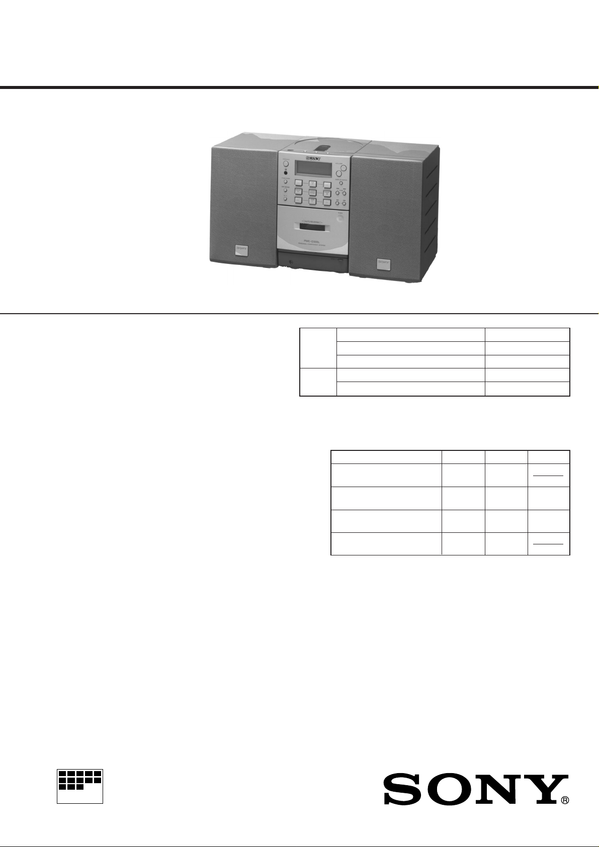
Photo: PMC-D305L
CD
Section
TAPE
Section
US Model
Canadian Model
E Model
Australian Model
PMC-D305
AEP Model
UK Model
PMC-D305L
Model Name Using Similar MechanismCFD-ZW150, ZW150L
CD Mechanism Type KSM-213CAM/C2NP
Optiacal Pick-up Name KSS-213B/S-RP
Model Name Using Similar Mechanism NEW
Tape Transport Mechanism Type MF-D305
For the US model
AUDIO POWER SPECIFICATIONS
POWER OUTPUT AND TOTAL
HARMONIC DISTORTION
With 6.0-ohm loads, both channels driven
from 100-15,000 Hz; rated 9.4 W per
channel-minimum RMS power, with no more
than
10 % total harmonic distortion in AC
operation.
CD player section
system
Compact disc digital audio system
Laser diode properties
Material: GaAlAs
Wave length: 780 nm
Emission duration: Continuous
Laser output: Less than 44.6 µW (This output is the
value measured at a distance of about 200 mm from
the objective lens surface on the optical pick-up
block with 7 mm aperture.)
Spindle speed
200 r/min (rpm) to 500 r/min (rpm) (CLV)
Number of channels
2
Frequency response
20-20,000 Hz + 1/– 2.5 dB
Wow and flutter
Below measurable limit
SPECIFICATIONS
Radio section
Frequency range
FM AM (MW) LW
US, Canadian, E 87.6 – 530 –
Models 108 MHz 1,710 kHz
AEP, UK, CET 87.6 – 531 – 153 –
Models 107 MHz 1,602 kHz279 kHz
Italian 87.5 – 531 – 153 –
Model 108 MHz 1,602 kHz279 kHz
Australian 87.6 – 531 –
Model 108 MHz 1,602 kHz
IF
FM: 10.7 MHz
AM (MW)/LW: 450 kHz
Aerials
FM: Lead aerial (D305)
FM: External aerial terminal (D305L)
AM (MW)/LW: External aerial terminal
– Continued on next page –
MICROFILM
PERSONAL COMPONENT SYSTEM
Page 2

Cassette-corder section
Recording system
4-track 2 channel stereo
Fast winding time
Approx. 130 s (sec.) with Sony cassette C-60
Frequency response
TYPE I (normal):40-15,000 Hz
General
Speaker
Full range: 8 cm (3 1/
Input
LINE IN jack (stereo minijack)
Minimum input level 250 mV
Outputs
Headphones jack (stereo minijack)
For 16-68 ohms impedance headphones
LINE OUT jack (stereo minijack)
Rated output level 440 mV at load impedance
47 kilohms
Optical digital output (optical output connector)
Wave length: 630 – 690 nm
Power output (excluding US model)
10 W + 10 W (at 6.0 ohms, 10% harmonic distortion)
Power requirements
For personal component system:
US, Canadian, E models 120 V AC, 60 Hz
AEP, UK, Italian, CET,
Australian models 230 V AC, 50 Hz
For remote commander:
3 V DC, 2 size AA (R6) batteries
Power consumption
AC 35 W
Dimensions (incl. projecting Parts)
Player: approx. 130 × 211 × 200 mm (w/h/d)
(5 1/8 × 8 3/8 × 7 7/8 inches)
Left speaker: approx. 125 × 210 × 234 mm
(w/h/d)
(5 × 8 3/8 × 9 1/4 inches)
Right speaker: approx. 125 × 210 × 200 mm
(w/h/d)
(5 × 8 3/8 × 7 7/8 inches)
Mass
Player: approx. 1.7 kg (3 lb. 12 oz)
Left speaker: approx. 2.8 kg (6 lb. 3 oz)
Right speaker: approx. 1.1 kg (2 lb. 7 oz)
Supplied accessories
Remote commander (1)
FM lead aerial (1) (D305L)
AM (MW)/LW loop aerial (1)
Audio connecting cord (1)
4
in.) dia., 6.0 ohms, cone type ×2
TABLE OF CONTENTS
1. SERVICING NOTES ............................................... 3
2. GENERAL ................................................................... 5
3. DISASSEMBLY.......................................................... 21
4. MECHANICAL ADJUSTMENTS ....................... 26
5. ELECTRICAL ADJUSTMENTS
Tape Deck Section ........................................................... 26
Tuner Section................................................................... 28
CD Section....................................................................... 30
6. DIAGRAMS
6-1. Printed Wiring Board
– Tuner Section – (PMC-D305) ...................................... 35
6-2. Schematic Diagram
– Tuner Section – (PMC-D305) ...................................... 37
6-3. Schematic Diagram
– Tuner Section – (PMC-D305L) .................................... 40
6-4. Printed Wiring Board
– Tuner Section – (PMC-D305L) .................................... 43
6-5. Printed Wiring Boards – CD Section –............................ 47
6-6. Schematic Diagram – CD Section – ................................ 49
6-7. Printed Wiring Boards – Main Section –......................... 52
6-8. Schematic Diagram – Main Section – ............................. 55
6-9. Schematic Diagram – Control Section – ......................... 58
6-10. Printed Wiring Boards – Control Section –..................... 61
6-11. Printed Wiring Boards – Power Section – ....................... 65
6-12. Schematic Diagram – Power Section – ........................... 67
6-13. IC Pin Function Description ............................................ 74
7. EXPLODED VIEWS ................................................ 76
8. ELECTRICAL PARTS LIST................................ 84
Design and specifications are subject to change without notice.
• Abbreviation
CET : East European, Russian
– 2 –
Page 3
r
SECTION 1
SERVICING NOTES
SAFETY CHECK-OUT
After correcting the original service problem, perform the following safety check before releasing the set to the customer:
Check the antenna terminals, metal trim, “metallized” knobs,
screws, and all other exposed metal parts for AC leakage. Check
leakage as described below.
LEAKAGE TEST
The AC leakage from any exposed metal part to earth ground and
from all exposed metal parts to any exposed metal part having a
return to chassis, must not exceed 0.5 mA (500 microampers).
Leakage current can be measured by any one of three methods.
1. A commercial leakage tester, such as the Simpson 229 or RCA
WT -540A. Follow the manufacturers’ instructions to use these
instruments.
2. A battery-operated AC milliammeter. The Data Precision 245
digital multimeter is suitable for this job.
3. Measuring the voltage drop across a resistor by means of a
VOM or battery-operated A C voltmeter. The “limit” indication
is 0.75 V, so analog meters must have an accurate low-voltage
scale. The Simpson 250 and Sanwa SH-63T rd are examples of
a passive VOM that is suitable. Nearly all battery operated digital
multimeters that have a 2 V AC range are suitable. (See Fig. A)
To Exposed Metal
Parts on Set
CHUCK PLATE JIG ON REPAIRING
On repairing CD section, playing a disc without the CD lid, use
Chuck Plate Jig.
• Code number of Chuck Plate Jig: X-4918-255-1
NOTES ON HANDLING THE OPTICAL PICK-UP
BLOCK OR BASE UNIT
The laser diode in the optical pick-up block may suffer electrostatic breakdown because of the potential difference generated by
the charged electrostatic load, etc. on clothing and the human body .
During repair, pay attention to electrostatic breakdown and also
use the procedure in the printed matter which is included in the
repair parts.
The flexible board is easily damaged and should be handled with
care.
0.15 µF
1.5 k
Ω
Earth Ground
AC
voltmete
(0.75 V)
Fig. A. Using an AC voltmeter to check AC leakage.
SAFETY-RELATED COMPONENT WARNING!!
COMPONENTS IDENTIFIED BY MARK ! OR DOTTED LINE
WITH MARK ! ON THE SCHEMATIC DIAGRAMS AND IN
THE PARTS LIST ARE CRITICAL TO SAFE OPERATION.
REPLACE THESE COMPONENTS WITH SONY PARTS WHOSE
PART NUMBERS APPEAR AS SHOWN IN THIS MANUAL
OR IN SUPPLEMENTS PUBLISHED BY SONY.
ATTENTION AU COMPOSANT AYANT RAPPORT
À LA SÉCURITÉ!
LES COMPOSANTS IDENTIFIÉS P AR UNE MARQ UE ! SUR
LES DIAGRAMMES SCHÉMATIQUES ET LA LISTE DES
PIÈCES SONT CRITIQUES POUR LA SÉCURITÉ DE
FONCTIONNEMENT . NE REMPLACER CES COM- POSANTS
QUE P AR DES PIÈCES SONY DONT LES NUMÉR OS SONT
DONNÉS DANS CE MANUEL OU D ANS LES SUPPLÉMENTS
PUBLIÉS PAR SONY.
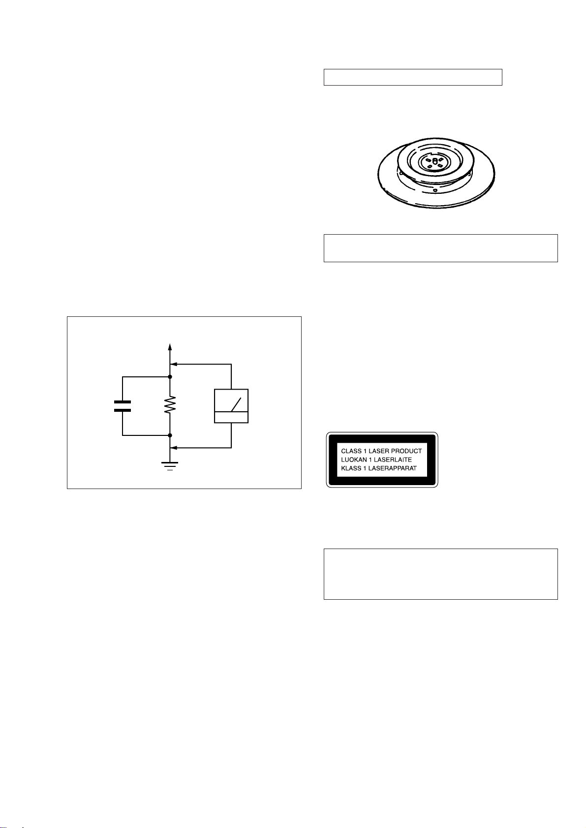
NOTES ON LASER DIODE EMISSION CHECK
The laser beam on this model is concentrated so as to be focused
on the disc reflective surface by the objective lens in the optical
pick-up block. Therefore, when checking the laser diode emission, observe from more than 30 cm away from the objective lens.
This Compact Disc player is classiffied as a
CLASS 1 LASER product.
The CLASS 1 LASER PRODUCT table is
location on the rear exterior.
CAUTION
Use of controls or adjustments or performance of procedures
other than those specified herein may result in hazardous radiation exposure.
– 3 –
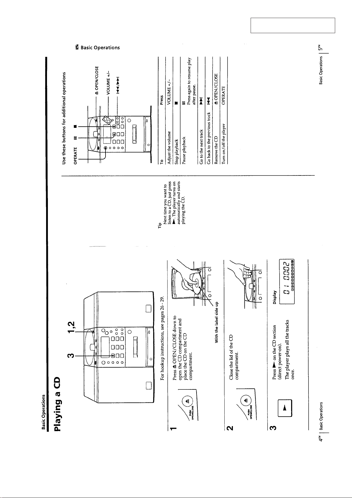
Page 4
LASER DIODE AND FOCUS SEARCH OPERATION
CHECK
1. Turn POWER switch on with to disc inserted and make Function switch to CD position.
2. Open the lid for CD.
3. Turn on S801 as following figure.
4. Press the · button.
5. Confirm the laser diode emission while observing the objecting
lens. When there is no emission, Auto Po wer Control circuit or
Optical Pick-up is broken.
Objective lens moves up and do wn three times for focus search.
S801
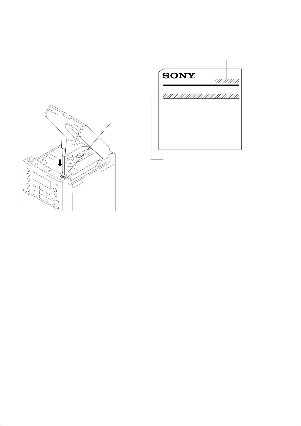
MODEL IDENTIFICATION
– Model Number Label – Carved on rear cabinet
PMC-D305
PMC-D305L
MODEL. No.
PERSONAL COMPONENT SYSTEM
MADE IN INDONESIA
US, Canadian, E models
AC: 120 V 60 Hz 35 W
AEP, UK, Italian, CET, Australian models
AC: 230 V ⁄ 50 Hz 35 W
• Abbreviation
CET: East European, Russian
HOW TO CHANGE THE FM CERAMIC FILTERS
This model is used two ceramic filters of CF1, 2 and CF3.
Therefore, the ceramic filter must change two pieces together since
it's supply two pieces in one package as a spare parts.
– 4 –
Page 5
SECTION 2
GENERAL
This section is extracted from
PMC-D305L’s instruction manual.
– 5 –
Page 6
– 6 –
Page 7
– 7 –
Page 8
– 8 –
Page 9
– 9 –
Page 10
– 10 –
Page 11
– 11 –
Page 12
– 12 –
Page 13
– 13 –
Page 14
– 14 –
Page 15
– 15 –
Page 16
– 16 –
Page 17
– 17 –
Page 18
– 18 –
Page 19
– 19 –
Page 20
– 20 –
Page 21
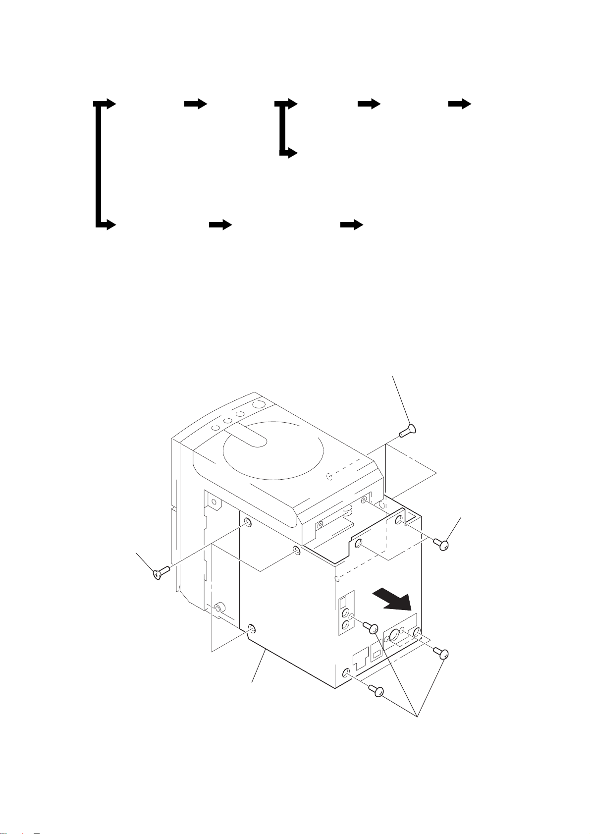
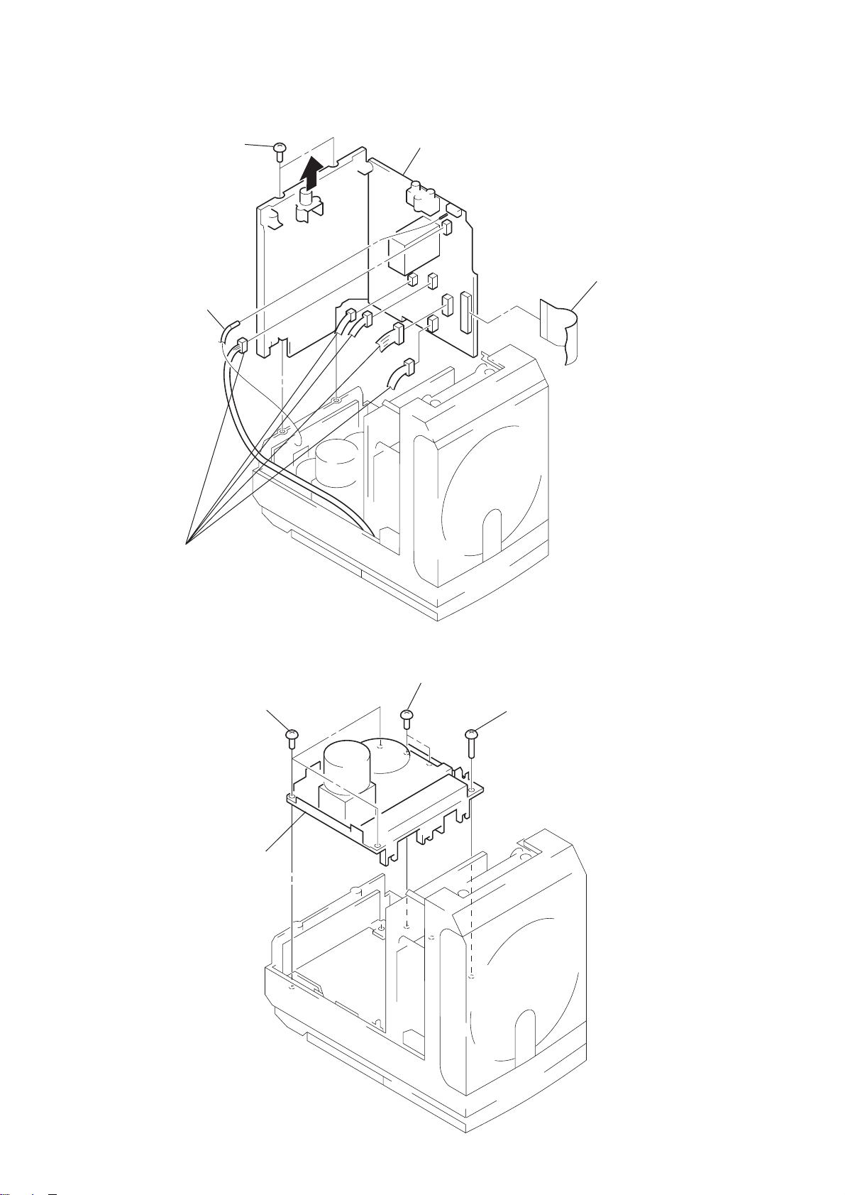
• This set can be disassembled in the order shown below.
SECTION 3
DISASSEMBLY
Set
Note: Follow the disassembly procedure in the numerical order given.
REAR CABINET
(Page 21)
FRONT (SP) SECTION
(Page 24)
CASE (LOWER)
SECTION
(Page 22)
TRANSFORMER,
CHASSIS (AMP) SECTION
(Page 25)
REAR CABINET
CD CABINET
SECTION
(Page 23)
TAPE MECHANISM DECK SECTION
(Page 22)
CD, CONTROL
BOARD
(Page 23)
POWER AMP,
TERMINAL, JACK BOARD
(Page 25)
1
three screws
(KTP 3
×
10)
OPTICAL PICK-UP
SECTION
(Page 24)
1
three screws
(KTP 3
×
10)
3
rear cabinet
2
five screws
(BVTP 3
2
two screws
(BVTP 3
×
10)
×
10)
– 21 –
Page 22
CASE (LOWER) SECTION
4
two screws
(BVTP 3
3
earth lead
×
10)
5
cabinet (lower) section
1
Parallel wire (27 core)
(CN303)
2
five connectors
(CN301, CNP302, 304, 306, 307)
TAPE MECHANISM DECK SECTION
2
three screws
(BVTP 3
3
tape mechanism
deck section
×
10)
1
three screws
(P 2.6
×
8)
2
screw
(BVTP 3
×
10)
– 22 –
Page 23
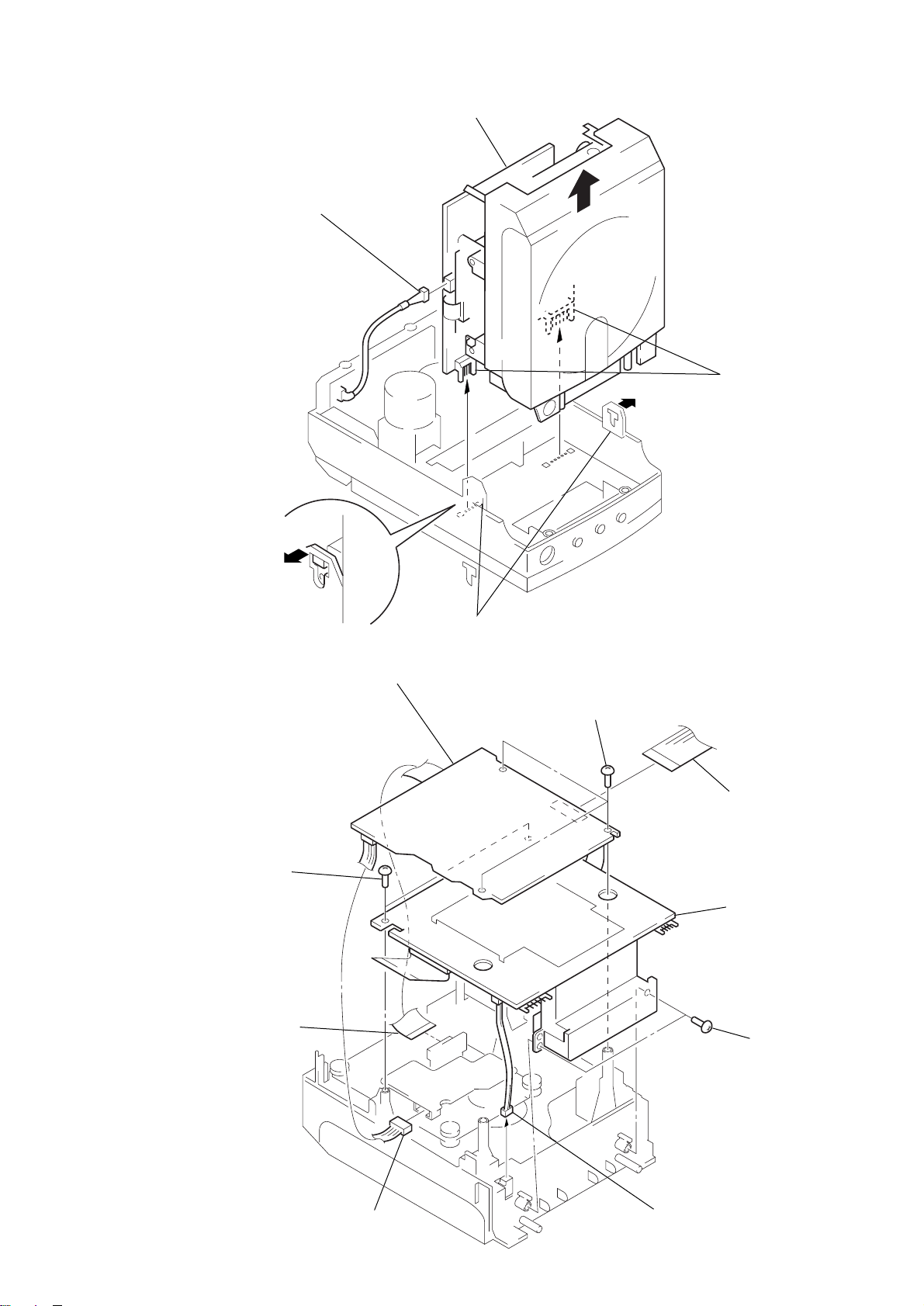
CD CABINET SECTION
1
connector
(CNP705)
4
CD cabinet section
3
two connectors
(CNP802, 803)
CD, CONTROL BOARD
8
two screws
(BVTP 3
2
FFC cable 16P
(optical pick-up)
×
10)
5
CD board
2
two claws
4
three screws
(BVTP 3
×
10)
3
Parallel wire (9 core)
(CNP706)
9
CONTROL board
7
two screws
(P 2.6
×
8)
1
connector
(CNP707)
– 23 –
6
connector
(S801)
Page 24

OPTICAL PICK-UP SECTION
1
four screws
(2.6
×
16)
2
optical pick-up section
FRONT (SP) SECTION
3
front (SP) section
4
connector
(CNP505)
1
two screws
(BVTP 3
×
10)
2
two screws
(P 3
×
30)
– 24 –
Page 25

)
TRANSFORMER, CHASSIS (AMP) SECTION
6
chassis (AMP)
section
1
connector
3
transformer
section
2
screw
(CNP505)
(BVTP 3
×
10)
5
two screws
(BVTP 3
×
10)
5
2
two screws
(BVTP 3
4
connector
(CNP503)
six screws
(BVTP 3
×
10)
×
10)
2
four screws
(BVTP 3
×
10)
5
three screws
(BVTP 3
×
10
POWER AMP, TERMINAL, JACK BOARD
1
1
two screws
(BVTP 3
×
screw
(BVTP 3
10)
×
10)
2
POWER AMP, TERMINAL,
JACK board
1
two screws
(BVTP 3
×
10)
– 25 –
Page 26

SECTION 4
r
MECHANICAL ADJUSTMENTS
SECTION 5
ELECTRICAL ADJUSTMENTS
PRECAUTION
1. Clean the following parts with a denatured-alcohol-moistened
swab:
record/playback head pinch roller
erase head rubber belts
capstan idlers
2. Demagnetize the record/playback head with a head demagnetizer. (Do not bring the head demagnetizer close to the erase
head.)
3. Do not use a magnetized screwdriver for the adjustments.
4. After the adjustments, apply suitable locking compound to the
parts adjusted.
5. The adjustments should be performed with the rated power supply voltage unless otherwise noted.
Torque Measurement
Mode Torque Meter Meter Reading
FWD
FWD 2.0-6.0 g•cm
Back tension (0.028-0.076 oz•inch)
FF CQ-201B
REW CQ-201B
CQ-102C
30-70 g•cm
(0.42-1.02 oz•inch)
80-170 g•cm
(1.12-2.38 oz•inch)
80-170 g•cm
(1.12-2.38 oz•inch)
T ape Tension Measurement
Mode Tension Meter Meter Reading
FWD CQ-403A more than 90 g (3.17 oz)
T APE DECK SECTION
0 dB=0.775 V
1. The adjustments should be perfomed in the order given in the
service manual. (As a general rule. Playback circuit adjustment
should be completed before performing recording circuit adjustment.)
2. The adjustments should be performed for both L-ch and R-ch
unless otherwise indicated.
Standard Output Level
SP OUT PHONES
Load impedance 6Ω 32Ω
Output level 0.775 V (0 dB) 0.25 V (–10 dB)
Test T ape
Type Signal Used for
WS-48B 3 kHz, 0 dB Tape speed adjustment
P-4-A063 6.3 kHz, –10 dB Head azimuth adjustment
Record/Playback Head Azimuth Adjustment
Procedure:
1. Mode: playback
test tape
P-4-A063
(6.3 kHz, –10 dB)
set
level mete
32
Ω
PHONES jack
+
–
2. Turn the adjustment screw for the maximum output lev els. If these
levels do not match, turn the adjustment screw
until both of out-
put levels match together within 1 dB.
L-CH
peak
Screw
position
R-CH
peak
output
level
within
1dB
L-CH
peak
R-CH
peak
within
1dB
Screw
angle
– 26 –
Page 27

3. Phase Check
Mode: playback
test tape
P-4-A063
(6.3 kHz, –10 dB)
L-CH
set
R-CH
in phase 45
32
32
PHONES jack
Screen pattern
°90°
Good Wrong
Ω
Ω
135°180
oscilloscope
H
V
+
+
–
–
°
4. After the adjustment, lock the screws with locking compound.
Adjustment Location:
Tape Speed Adjustment
Procedure:
Mode: playback
speed checker
LFM-30 or
digital frequency
32
counter
Ω
test tape
WS-48B
(3 kHz, 0dB)
set
PHONES jack
Adjustment V alues:
Speed checker Digital frequency counter
–1% to +1% 2,970 to 3,030 Hz
Frequency difference between the beginning and the end of the
tape should be within 1% (30 Hz).
Adjustment Location:
adjustable
resistor
M691
forward
reverse
screwdriver
– 27 –
Page 28

TUNER SECTION
l
r
Precautions in Repairing
Note: As a FM front-end (TU1) is difficult to repair if faulty, replace it
with new one.
[AM]
FUNCTION Switch: RADIO
BAND Switch: AM, MW, LW
AM RF SSG
30% amplitude modulation by
400 Hz signal
output level: as low as possible
[FM]
FUNCTION Switch: RADIO
BAND Switch: FM
FM RF SSG
22.5 kHz frequency deviation
by 400 Hz signal.
output level: as low as possible
32
set
PHONES jack
Put the lead-wire
antenna close to
the set.
0.01
to ANT IN termina
level meter
Ω
+
–
µ
F
AM IF ADJUSTMENT
Adjust for a maximum reading on level meter.
CFT1 450 kHz
(D305)
AM FREQUENCY COVERAGE CONFIRM
Confirm for a reading on digital voltmeter.
Confirm 530 kHz <531 kHz> 1.0 ±0.5 V
Confirm 1,710 kHz <1611 kHz> 5.0 ± 1.0 V <4.8 ± 1.0 V>
Note: Not use the AM RF signal generator in this confirm.
< >: Australian model
(D305)
AM TRACKING ADJUSTMENT
Adjust for a maximum reading on level meter.
L3 620 kHz
CT2 1,400 kHz
(D305L)
MW FREQUENCY COVERAGE CONFIRM
Confirm for a reading on digital voltmeter.
Confirm 531 kHz 0.85 ± 0.5 V
Confirm 1611 kHz 6.8 ± 1.5 V
Note: Not use the AM RF signal generator in this confirm.
(D305L)
MW TRACKING ADJUSTMENT
Adjust for a maximum reading on level meter.
L3 621 kHz
CT4 1,404 kHz
digital voltmete
TP (VT)
+
–
• Repeat the procedures in each adjustment several times, and the
frequency coverage and tracking adjustments should be finally
done by the trimmer capacitors.
• Abbreviation
D305: PMC-D305
D305L: PMC-D305L
(D305L)
LW FREQUENCY COVERAGE ADJUSTMENT
Adjust for a reading on digital voltmeter.
Confirm 153 kHz 0.7 ± 0.5 V
L4 279 kHz 7.5 ± 0.2 V
Note: Not use the AM RF signal generator in this adjustment.
(D305L)
LW TRACKING ADJUSTMENT
Adjust for a maximum reading on level meter.
L5 162 kHz
CT5 261 kHz
(D305)
FM FREQUENCY COVERAGE ADJUSTMENT
Adjust for a reading on digital voltmeter.
L2 87.5 MHz 1.6 ± 0.4 V
Confirm 108 MHz 6.5 ± 0.5 V
Note: Not use the FM RF signal generator in this adjustment.
(D305)
FM TRACKING ADJUSTMENT
Adjust for a maximum reading on level meter.
L1 87.5 MHz
CT1 108 MHz
Adjustment Location: TUNER board (See page 29.)
– 28 –
Page 29

Adjustment Location:
• PMC-D305
L2
FM Frequency
Coverage
Adjustment
[TUNER BOARD]
(Component Side)
IC1
CFT1
AM IF Adjustment
L1
FM T rac king
Adjustment
CT1
L4
AM Frequency
Coverage
Adjustment
• PMC-D305L
[TUNER BOARD]
(Component Side)
TU1
L3
AM Tracking
CT2
Adjustment
CFT1
AM IF Adjustment
L4
MW/LW Frequency
Coverage
Adjustment
IC1
– 29 –
L3
CT4
MW T racking
Adjustment
CT5
L5
LW Tracking
Adjustment
Page 30

Ver 1.2 1999. 11
CD SECTION
Notes on Adjustment
1. Perform adjustment in test mode.
After adjustments, be sure to release test mode.
2. Perform adjustments in the order given.
3. Use the disc (YEDS-18. Part No. 3-702-101-01) only when so
indicated.
How to Put the Set into Test Mode
1. Disconnect an AC plug cord.
2. Turn on the power while shorting the test point (TEST1). (Connect the AC plug cord)
3. Opening the shorted test point puts the set into Test Mode.
[SW (A) BOARD] (Conductor Side)
TEST 1
Terminal
E-F Balance Adjustment
This adjustment is to be done when the optical pick-up is replaced.
Procedure:
Oscilloscope
(DC range)
CD board
TP (TRACKING-Y)
TP (VC)
+
–
1. Connect the oscilloscope to TP (TRACKING-Y) and TP (VC)
on the CD board.
2. Insert the disc (YEDS-18) in and close the lid for CD.
3. Put the set into test mode.
4. Press the + and = buttons to move the optical pick-up to
the center.
5. Press the ( button.
From focus searching, focus is turned ON while entering
CLV drawing-in mode. Tracking and sled are turned OFF.
6. Adjust RV703 so that the oscilloscope traverse w aveform is symmetrical, as shown in the figure below.
Note: Take long sweep time
VOLT/DIV: 0.2 V (with the 10:1 probe in use.)
TIME/DIV: 1 ms
for easy monitoring.
How to Release the Test Mode
1. Press the [OPERATE] button to put the set into the standby
status.
2. Finally, disconnect and connect the AC plug cord.
Before Begining Adjustment
Put the set into test mode and perform the following checks.
Repair if there are any problems.
• Sled Motor Check
Press the +, = buttons and confirm that the optical pick-up
moves smoothly from the innermost to outermost circumference
and back smoothly and with no catching or abnormal noises.
+ : Optical pick-up moves to the outer circumference
= : Optical pick-up moves to the inner circumference
• Focus Search Check
1. Press the ( button. (Focus search operation is performed continuously.)
2. Look at the optical pick-up objective lens and confirm that it
moves up and down smoothly, when no catching or abnormal
noises.
3. Press the p button.
Confirm that focus search operation stops. If it does not , press
the p button again longer.
A
0 V
A=B
B
0 V
Adjustment value: 0.4 ± 0.2 Vp-p (A + B)
7. Release the test mode after adjustment is completed.
Adjustment Location: CD board (See page 33.)
A
B
A=B
Note: When the malfunction is occurred by mis-passing other keys, turn
off the power and check again from making the test mode.
– 30 –
Page 31

Focus Bias Adjustment
This adjustment is to be done when the optical pick-up is replaced.
Procedure:
Oscilloscope
(AC range)
CD board
TP (RF)
TP (VC)
+
–
1. Connect the oscilloscope TP (RF) and TP (VC) on the CD board.
2. Insert the disc (YEDS-18) in and close the lid for CD.
3. Put the set into test mode. (See page 30.)
4. Press + and = buttons to move the optical pick-up to the
center. (Move the optical pick-up to the music area on the disc
to enable easy visibility of the eye pattern.)
5. Press the ( button.
From focus searching, focus is turned ON while entering
CLV drawing-in mode. Tracking and sled are turned OFF.
6. Press the ( button.
[Both tracking and sled are turned ON.]
7. Adjust RV701 so that the oscilloscope wa veform is as sho wn in
the figure below. (eye pattern)
A good eye pattern means that the diamond shape (≈ ) in the
center of the waveform can be clearly distinguished.
• RF signal reference waveform (eye pattern)
VOLT/DIV : 0.2 V (With the 10:1 probe in use)
TIME/DIV : 500 ns
1.3
±
0.2 Vp-p
REFERENCE
Focus/Tracking Gain Adjustment
A frequency responce analyzer is necessary in order to perform
this adjustment exactly.
However, this gain has a margin, so even if it is slightly off, there
is no problem. Therefore, do not perform this adjustment.
Focus/tracking gain determines the pick-up follow-up (vertical and
horizontal) relative to mechanical noise and mechanical shock
when the 2-axis device operate.
However , as these reciprocate, the adjustment is at the point where
both are satisfied.
• When gain is raised, the noise when the 2-axis device operates
increases.
• When gain is lowered, mechanical shock and skipping occurs
more easily.
• When gain adjustment is off, the symptoms below appear.
Gain
Symptoms
• The time until music starts becomes
longer for p→( on automatic
selection. low low or high
(=, + buttons pressed.)
(Normally takes about 2 seconds.)
• Music does not start and disc
continues to rotate for p→( or
automatic selection.
(=, + buttons pressed.)
• Sound is interrupted during PLAY.
Or time counter display stops – low
progressing.
• More noise during 2-axis device
operation.
Focus Tracking
–low
high high
When observing the eye pattern, set the oscilloscope for AC
range and raise vertical sensitivity.
8. Release the test mode after adjustment is completed.
Adjustment Location: CD board (See page 33.)
– 31 –
Page 32

The following is a simple adjustment method.
– Simple Adjustment –
Note: Since exact adjustment cannot be performed, remember the posi-
tions of the controls before performing the adjustment. If the positions after the primary adjustment are only a little different, return
the controls to the original position.
oscillosope
(DC range)
CD board
8. Connect the oscilloscope to TP (TRACKING-Y) and TP (VC)
on the CD board.
9. Adjust RV704 so that the waveform is as shown in the figure
below. (tracking gain adjustment)
VOLT/DIV: 1 V
TIME/DIV:2 ms
0 V
TP (FOCUS-Y)
TP (TRACKING-Y)
TP (VC)
+
–
Procedure:
1. Keep the set horizontal.
If the set is not horizontal, this adjustment cannot be performed
due to the gravity against the 2-axis device.
2. Connect the oscilloscope TP (FOCUS-Y) and TP (VC) on the
CD board.
3. Insert the disc (YEDS-18) in and close the lid for CD.
4. Put the set into test mode. (See page 30.)
5. Press the ( button.
From focus searching, focus is turned ON while entering
CLV drawing-in mode. Tracking and sled are turned OFF.
6. Press the ( button.
[Both tracking and sled are turned ON.]
7. Adjust RV702 so that the waveform is as shown in the figure
below. (Focus gain adjustment)
VOLT/DIV: 100 mV
TIME/DIV:2ms
100 mV
0 V
• Inconnect Examples (DC level changes more than on adjusted
waveform)
• Incorrect Examples (fundamental wave appears)
low tracking gain
VOLT/DIV: 1 V
TIME/DIV: 2ms
0 V
high tracking gain
high fandamental wave
than for low gain
VOLT/DIV: 1 V
TIME/DIV: 2ms
0 V
Note:
VOLT/DIV: with the 10:1 probe in used.
10. Release test mode after adjustment is completed.
Adjustment Location: CD board (See page 33.)
low focus gain
high focus gain
VOLT/DIV: 100 mV
TIME/DIV:2ms
250 mV
0 V
VOLT/DIV: 100 mV
TIME/DIV:2ms
100 mV
75 mV
0 V
– 32 –
Page 33

SECTION 6
DIAGRAMS
Connection and Adjustment Location: • Circuit Boards Location
[CD BOARD]
(Conductor Side)
TP
(RF)
TP
(FOCUS-Y)
HEADPHONE board
LAMP board
SW (A) board
HEAD board
SW (B) board
CONTORL board
CD board
CD MOTOR board
AUDIO board
SW board
[CD BOARD]
(Component Side)
CNP706
RV701
FOCUS BIAS
TP
(TRACKING-Y)
RV703
E-F BALANCE
RV704
TRACKING GAIN
CNP701
RV702
FOCUS GAIN
TP
(VC)
LINE board
TERMINAL board
TUNER board
JACK board
POWER AMP board
– 33 –
POWER board
– 34 –
Page 34

Page 35

Page 36

Page 37

Page 38

Page 39

Page 40

Page 41

Page 42

Page 43

Page 44

Page 45

Page 46

• Wavef orms
– CD Section –
1 IC701 #¡ (RFO)
200 mV/DIV, 500 ns/DIV
Note: This waveform is measured
between RFO and VC.
2 IC701 $¢ (TI)
100 mV/DIV, 100 ns/DIV
1.3 ± 0.2 Vp-p
6 IC702 @∞ (XPCK)
2 V/DIV, 200 ns/DIV
240 ns
7 IC702 #∞ (XTAO)
2 V/DIV, 50 ns/DIV
4.8 Vp-p
• IC Block Diagrams
– CD Section –
IC701 CXA1782BQ
PHD2
PHD1
36
35 34
PHD
–
RF IV AMP1
LD
33
+
–
+
APC
–
+
RF M
32
–
–
+
+
FOK
+
LEVELS
–
RF O
31
–
+
–
+
MIRR
RF I
30
–
+
+
–
+
–
29CP28
CB
DFCT
CC126CC225FOK
27
–
+
24 SENS
+
–
IIL
TTL
23 C. OUT
3 IC701 2 (FI)
100 mV/DIV, 100 ns/DIV
4 IC702 @º (LRCK)
2 V/DIV, 10 µs/DIV
Approx. 50 mVp-p
Approx. 50 mVp-p
5 Vp-p
16.9344 MHz
4.8 Vp-p
–
+
F IV AMP
BAL1
BAL2
TOG1
TOG2
• WINDOW COMP
RF IV AMP2
–
+
–
+
E IV AMP
BAL3
TOG3
ATSC
–
+
FE AMP
TE AMP
TTL
+
–
IIL
FZC COMP
+
–
TZC COMP
DFCT
DFCT
FS4
• IIL DATA RESISTOR • INPUT SHIFT RESISTOR
–
+
–
+
–
+
+
–
TM1
TOG1-3 FS1-4 TG1-2 TM1-7 PS1-4
BAL1-3
–
–
+
+
HPF COMP LPF COMP
• FCS PHASE
COMPENSATION
FS2
+
–
• ADDRESS DECODER
• OUTPUT DECODER
• TRACKING
• PHASE
COMPENSATION
TG1
FS1
• ISET
TM6
TM5
TM4
TM3
TM7
TG2
37FE BIAS
38F
39E
40EI
41VEE
42TEO
43LPFI
44TEI
45ATSC
46TZC
47TDFCT
48VC
TTL
IIL
–
TM2
+
• F SET
22 XRST
21 DATA
20 XLT
19 CLK
18 VCC
17 ISET
16 SL 0
+
15 SL M
14 SL P
1312TA O
–
22.6 µs
5 IC702 @™ (BCK)
2 V/DIV, 200 ns/DIV
280 ns
6.7 Vp-p
– 69 –
3
2
1
FEI
FEO
FDFCT
4
FLB
FGD
FE O
FE M
SRCH
TGU
TG2
FSET
TA M
11
10
9
8
7
6
5
– 70 –
Page 47

IC702 CXD2507AQ
XLON
SPOD
SPOC
SPOB
SPOA
CLKO
DD
XLTO
DATO
CNIN
SEIN
CLOK
V
XLAT
52535455565758596061626364
FOK
MON
MDP
MDS
LOCK
TEST
FILO
FILI
PCO
VSS
AVSS
CLTV
AVDD
BIAS
ASYI
ASYO
ASYE
WDCK
1
2
3
4
5
6
7
8
9
10
11
12
13
14
RF
15
16
17
18
19
SERVO AUTO
SEQUENCER
14
INTERFACE
DIGITAL
PLL
ASYMMETRY
CORRECTOR
5
CPU
LRCK
PCMD
RAM
BCLK
5
DEMODULATOR
16K
XUGF
GTOP
SUB CODE
PROCESSOR
EFM
3
ERROR
CORRECTOR
3
DD
V
XPCK
4
D/A
INTERFACE
GFS
RFCK
CZPO
DIGITAL
6
XROF
CLV
MNT3
32313029282726252423222120
DIGITAL
MNT1
OUT
CLOCK
GENERATOR
51
DATA
XRST
50
SENS
49
MUTE
48
SQCK
47
SQSO
46
45
EXCK
SBSO
44
SCOR
43
42
SS
V
WFCK
41
EMPH
40
DOUT
39
C4M
38
37
FSTT
XTSL
36
XTAO
35
XTAI
34
33
MNTO
IC703 BA6898FP
– 71 –
Page 48

IC704 SM5877AM
– MAIN Section –
IC301 TA2068N
– 72 –
Page 49

IC305 BA338
– 73 –
Page 50

6-13. IC PIN FUNCTION DESCRIPTION
CONTROL BOARD IC801 CXP83120A-019Q (SYSTEM CONTROL, LCD DRIVE)
Pin No. Pin Name I/O Function
1 AC CHK I AC check input
2 C-SCOR I CD-SCOR input
3 RMC I Remote commander input
4 C-XRST O CD system reset output
5 C-XLAT O CD DSP (IC702) command
6 C-DAT O CD DSP (IC702) command data output
7 C-CLK O Clock output for CD DSP (IC702) command
8 C-DOOR I Open/close detection input “L”: close “H”: open
9 328/332 I 328/332 select input (Fixed at “H”)
10 C-SENC I CD-SENS input
11 C-SQCK O Clock output for CD SUBQ
12 C-SQSO I CD SUBQ input
13 T-BIAS I Tape REC BIAS input
14 – – Not used (Open)
15 T-REC I Tape REC input
16 T-SOL O Plunger control output
17 T-MODE O HEAD switching output
18 T-AMS I AMS sensitivitiy switching
19 T-MCON O Motor control output “H”: Motor on
20 P-CON O Power on/off control output
21 V-CLK O Volume clock output
22 V-DAT O Volume data output
23 V-CE O Electrical volume (IC302) chip enable output
24 R-ST I Stereo detection input
25 R-COUNT I Tuner PLL IC count input
26 R-DAT O Tuner PLL IC data output
27 R-CLK O Tuner PLL IC clock output
28 R-CE O Tuner PLL IC chip enable output
29 9K/10K I 9K/10K select input (Not used)
30 T-STAT I Tape detection input
31-34 KEY-0-3 I Key return signal input
35 INIT O Initial setting output
36 SIMUKE I Destination setting terminal
37 SFC O Shift clock on/off out
38 RST I Reset input
39 EXTAL1 I Clock oscillation input (4.19MHz)
40 XTAL1 O Clock oscillation output (4.19MHz)
41 VSS – Ground (for A/D converter)
42 XTAL2 O Clock oscillation output (Open)
43 EXTAL2 I Clock oscillation output (Fixed at “L”)
44 AVREF I Reference voltage input (for A/D conver ter)
45 AVSS – Ground (for A/D converter)
– 74 –
Page 51

Pin No. Pin Name I/O Function
46 VL O LCD bias resistor current control terminal (Cut off at standby)
47-49 VLC3-1 – LCD bias power supply terminal
50-53 COM0-3 O LCD common signal output terminal
54-77 SEG0-23 O LCD segment signal output terminal
78-84 NC – Not used (Open)
85-87 – – Not used (Open)
88 BL-CONT O LCD Back light control output
89 VDD – Power supply (+5V)
90 NC – Connected to the power supply
91 VSS – Ground
92 TX O Crystal connection for clock oscillation (32.768kHz)
93 TEX I Crystal connection for clock oscillation (32.768kHz)
94 C-MUTE O Mute output for CD
95 B-MUTE O Mute output for Tuner
96 A-MUTE O Mute output for Audio
97 ISS1 I ISS1 switch input
98 ISS2 I ISS2 switch input
99 T-END I Tape end detection input
100 NC – Not used (Open)
– 75 –
Page 52

SECTION 7
EXPLODED VIEWS
NOTE:
• -XX and -X mean standardized parts, so they
may have some difference from the original one.
• Color Indication of Appearance Parts
Example:
KNOB, BALANCE (WHITE) . . . (RED)
↑↑
Parts Color Cabinet's Color
• Abbreviation
CND : Canadian CET : East European, Russian
IT : Italian AUS : Australian
(1) CASE SECTION
• Items marked “*” are not stocked since they
are seldom required for routine service. Some
delay should be anticipated when ordering these
items.
• The mechanical parts with no reference number in the exploded views are not supplied.
• Hardware (# mark) list and accessories and
packing materials are given in the last of the
electrical parts list.
CD cabinet section
#2
The components identified by mark
! or dotted line with mark ! are
critical for safety.
Replace only with part number
specified.
Les composants identifiés par une
marque ! sont critiquens pour la
sécurité.
Ne les remplacer que par une pièce
portant le neméro spécifié.
#1
4
#2
#1
3
front cabinet
section
#1
#1
5
#1
2
1
6
1
Ref. No. Part No. Description Remark
1 3-014-503-01 FOOT
* 2 A-3306-626-A TUNER BOARD, COMPLETE (D305L)
* 2 A-3306-831-A TUNER BOARD, COMPLETE (D305: AUS)
* 2 A-3306-834-A TUNER BOARD, COMPLETE
(D305: US, CND, E)
3 1-782-296-11 WIRE, PARALLEL (FFC) (27 CORE)
Ref. No. Part No. Description Remark
4 3-014-125-01 CABINET (REAR)
* 5 A-3306-627-A AUDIO BOARD, COMPLETE (D305L)
* 5 A-3306-835-A AUDIO BOARD, COMPLETE (D305)
6 3-014-127-01 CASE (LOWER)
– 76 –
Page 53

6
(2) FRONT CABINET SECTION
53
54
55
#3
56
#3
#4
57
67
#3
66
58
#5
65
#3
#1
64
#1
62
MF-D305
63
61
59
#1
#3
#
60
52 51
Ref. No. Part No. Description Remark
51 X-3373-799-1 LID (TERMINAL) ASSY
52 X-3373-798-1 LID (CASSETTE) ASSY (D305L)
52 X-3374-255-1 LID (CASSETTE) ASSY (D305)
53 X-3373-797-1 PANEL (FRONT) ASSY (D305L)
53 X-3374-254-1 PANEL (FRONT) ASSY (D305)
54 3-014-091-01 BUTTON (MAIN)
55 3-014-090-01 CABINET (FRONT)
56 3-014-092-01 BUTTON (UPPER)
* 57 1-666-185-11 SW (B) BOARD
* 58 1-666-184-11 SW (A) BOARD
Ref. No. Part No. Description Remark
59 3-014-097-01 PLATE (CASSETTE), LOCK
60 3-014-098-01 RETAINER (CASSETTE), LOCK
61 3-013-735-01 SPRING (CASSETTE LOCK)
62 3-014-100-01 HOLDER (TERMINAL)
* 63 A-3306-625-A LINE BOARD, COMPLETE (D305L)
* 63 A-3306-833-A LINE BOARD, COMPLETE (D305)
64 3-014-102-01 SPRING (CASSETTE)
65 3-014-096-01 HOLDER (CASSETTE)
66 3-014-103-01 SPRING (TERMINAL LID)
67 3-343-248-01 DAMPER (P), SMALL
– 77 –
Page 54

(3) CD CABINET SECTION
107
110
109
105
#3
#3
102
108
106
#3
104
#1
103
#1
120
S801
117
119
113
114
#7
111
112
115
116
117
101
#1
Ref. No. Part No. Description Remark
* 101 A-3306-628-A CD BOARD, COMPLETE (D305: AUS/D305L)
* 101 A-3306-837-A CD BOARD, COMPLETE (D305: US, CND, E)
102 1-782-294-11 WIRE, PARALLEL (FFC) (9 CORE)
* 103 A-3306-631-A CONTROL BOARD, COMPLETE (D305L)
* 103 A-3306-832-A CONTROL BOARD, COMPLETE (D305: AUS)
* 103 A-3306-836-A CONTROL BOARD, COMPLETE
(D305: US, CND, E)
* 104 1-666-187-11 HEADPHONE BOARD
* 105 1-666-186-11 LANP BOARD
106 3-014-123-01 CABINET (CD)
107 3-014-129-01 WINDOW (CD)
108 3-351-377-11 DAMPER
109 3-014-128-01 SPRING (CD)
KSM-213CAN/C2NP
118
Ref. No. Part No. Description Remark
110 3-014-124-01 LID (CD)
111 1-452-732-11 MAGNET
112 3-910-112-01 PLATE, CHUCKING
113 3-014-131-01 LEVER
* 114 3-014-132-01 SPRING, COMPRESSION
115 3-910-116-01 COVER, CD
116 3-910-095-11 RUBBER, VIBRATION PROOF (RED)
117 3-916-006-01 SCREW (2.6X16)
118 1-639-678-12 CD MOTOR BOARD
119 3-910-095-01 RUBBER, VIBRATION PROOF (GREEN)
120 1-769-069-11 CABLE, FFC 16P
S801 1-692-960-11 SWITCH, PUSH (1 KEY) (OPEN/CLOSE)
– 78 –
Page 55

(4) OPTICAL PICK-UP SECTION
(KSM-213CAN/C2NP)
not supplied
151
not supplied
152
#8
153
M701
M702
Ref. No. Part No. Description Remark
! 151 8-848-376-11 OPTICAL PICK-UP KSS-213B/S-RP
152 2-627-003-02 GEAR (B) (RP)
153 2-626-908-01 SHAFT, SLED
The components identified by
mark ! or dotted line with
mark ! are critical for safety.
Replace only with part number
specified.
Ref. No. Part No. Description Remark
M701 X-2625-770-1 CHASSIS ASSY (MB) (RP), MOTOR (SPINDLE)
M702 X-2625-769-1 GEAR ASSY (MB), MOTOR (SLED)
Les composants identifiés par une
marque ! sont critiques pour la
sécurité.
Ne les remplacer que par une pièce
portant le neméro spécifié.
– 79 –
Page 56

(5) TAPE MECHANISM DECK SECTION-1
(MF-D305)
214
209
211
208
HRPE101
207
212
210
205
216
215
213
217
206
202
201
Ref. No. Part No. Description Remark
201 3-938-905-01 HEAD, LEVER
202 3-938-940-01 SPRING (L)
203 3-938-941-01 SCREW (A)
204 3-938-906-01 AZIMUTH, SPRING
205 3-017-432-01 SPRING (A)
206 3-938-901-01 HEAD, HOLDER
* 207 3-938-904-01 HEAD, FRAME
208 3-938-902-01 WASHER
209 3-938-903-01 SCREW
210 3-938-935-01 SPRING (G)
203
204
226
224
225
220
222
223
221
218
227
219
Ref. No. Part No. Description Remark
* 215 3-938-916-01 BRAKE, ARM
* 216 3-938-914-01 FRAME (C)
* 217 3-938-913-01 FRAME (B)
* 218 3-938-909-01 LOCK, EJECT
219 3-938-944-01 SCREW (D)
220 3-017-591-01 ARM (PINCH R) ASSY
221 3-938-937-01 SPRING (I)
222 3-938-938-01 SPRING (J)
* 223 3-938-911-01 HEAD (B), CHASSIS
224 3-938-907-01 HEAD, GEAR ARM
* 211 X-3372-610-1 ASSIST ASSY, LEVER
212 3-938-933-01 SPRING (E)
213 3-017-592-01 ARM (PINCH L) ASSY
214 3-938-934-01 SPRING (F)
225 3-938-943-01 SCREW (C)
226 3-938-942-01 SCREW (B)
* 227 1-662-743-11 HEAD BOARD
HRPE1011-500-480-11 HEAD, MAGNETIC (REC/PB/ERASE)
– 80 –
Page 57

(6) TAPE MECHANISM DECK SECTION-2
(MF-D305)
255
259
257
258
256
261
254
262
255
260
253
263
252
PM691
251
264
265
266
not
supplied
267
275
268
286
285
269
270
273
274
275
282
261
276
284
M691
271
272
277
278
279
280
283
281
Ref. No. Part No. Description Remark
251 3-938-949-01 WASHER (A)
252 3-938-951-01 WASHER (D)
253 3-938-936-01 SPRING (H)
254 3-938-930-01 SPRING (B)
255 3-938-910-01 REEL, CAP
* 256 3-938-912-01 ARM (UD)
257 3-938-952-01 WASHER (E)
258 3-938-948-01 WASHER (B)
259 3-938-932-01 SPRING (D)
260 3-938-908-01 CASSETTE, SPRING
261 3-938-945-01 SCREW (E)
262 3-017-428-01 FRAME (D)
263 3-938-920-01 PLUNGER, K
264 3-938-918-01 TRIGGER, ARM
265 3-938-931-01 SPRING (C)
266 3-938-921-01 GEAR (REEL)
267 3-662-742-11 SW BOARD
268 3-938-954-01 WASHER (G)
269 3-938-947-01 SCREW (G)
Ref. No. Part No. Description Remark
270 3-017-431-01 BRACKET (MM)
271 3-017-430-01 BELT
272 3-017-596-01 FLYWHEEL (R) ASSY
273 3-017-434-01 SCREW (H)
274 3-017-595-01 FLYWHEEL (L) ASSY
275 3-938-950-01 WASHER (C)
276 3-017-433-01 SPRING (K)
277 3-938-946-01 SCREW (F)
* 278 3-938-919-01 ARM (FR)
279 3-017-435-01 REFLECTOR
280 3-017-429-01 GEAR (REF)
281 3-938-917-01 GEAR (A)
282 3-938-924-01 GEAR (P)
283 3-938-923-01 GEAR (FR)
284 X-3372-613-1 CLUTCH ASSY
285 3-938-925-01 GEAR (IDL)
286 3-938-922-01 GEAR (CAM)
M691 3-016-425-01 MOTOR ASSY (CARSTAN/REEL)
PM691 1-454-806-11 SOLENOID, PLUNGER
– 81 –
Page 58

(7) SPEAKER (L) SECTION
303
#1
304
#1
#1
305
#1
302
SP101
#1
316
not supplied
306
#1
D305: AUS/
D305L
#1
#9
#10
#1
#10
314
315
307
312
not
supplied
#1
#1
#1
#1
308
309
310
#11
AEP, IT, CET
E
US, CND
AUS
301
Ref. No. Part No. Description Remark
301 X-3374-211-1 FRONT SUB ASSY
* 302 1-666-177-11 POWER AMP BOARD
* 303 1-666-178-11 TERMINAL BOARD
* 304 1-666-179-11 JACK BOARD
305 3-014-113-01 CHASSIS (AMP)
306 1-782-509-11 CORD, SPEAKER
307 3-014-110-01 CABINET (REAR.SP-L)
308 X-3374-496-1 CORD ASSY
* 309 3-014-106-01 STOPPER (4P), CORD
! 310 1-575-651-11 CORD, POWER (D305L: AEP, IT, CET)
! 310 1-575-653-11 CORD, POWER (D305: E)
! 310 1-696-847-11 CORD, POWER (D305: AUS)
313
311
T501
The components identified by
mark ! or dotted line with
mark ! are critical for safety.
Replace only with part number
specified.
Ref. No. Part No. Description Remark
! 310 1-751-520-11 CORD, POWER (D305L: UK)
! 310 1-769-743-11 CORD, POWER (D305: US, CND)
311 3-703-244-00 BUSHING (FBS001), CORD (EXCEPT D305: E)
311 4-966-266-01 BUSHING (S) (FBS002), CORD (D305: E)
312 3-014-503-01 FOOT
* 313 1-666-176-11 POWER BOARD
314 4-812-134-11 RIVET (DIA. 3.5), NYLON (D305: AUS/D305L)
* 315 3-017-037-01 INSULATOR (D305: AUS/D305L)
316 3-017-101-01 LABEL, FUSE RATING (D305: US, CND, E)
SP101 1-505-607-11 SPEAKER (8CM) (L-CH)
! T501 1-431-353-11 TRANSFORMER, POWER (D305: AUS/D305L)
! T501 1-431-354-11 TRANSFORMER, POWER (D305: US, CND, E)
not supplied
Les composants identifiés par une
marque ! sont critiques pour la
sécurité.
Ne les remplacer que par une pièce
portant le neméro spécifié.
UK
– 82 –
Page 59

(8) SPEAKER (R) SECTION
351
#1
352
#1
353
#1
355
#11
SP201
Ref. No. Part No. Description Remark
351 X-3374-211-1 FRONT SUB ASSY
352 1-782-509-11 CORD, SPEAKER
353 3-014-104-01 CABINET (REAR.SP-R)
354
Ref. No. Part No. Description Remark
354 3-014-503-01 FOOT
* 355 3-014-109-01 STOPPER, CORD
SP201 1-505-607-11 SPEAKER (8CM) (R-CH)
– 83 –
Page 60

AUDIO
SECTION 8
ELECTRICAL PARTS LIST
NOTE:
• Due to standardization, replacements in the
parts list may be different from the parts specified in the diagrams or the components used on
the set.
• -XX and -X mean standardized parts, so they
may have some difference from the original one.
• RESISTORS
All resistors are in ohms.
METAL: Metal-film resistor.
METAL OXIDE: Metal oxide-film resistor.
F: nonflammable
• Abbreviation
CND : Canadian CET : East European, Russian
IT : Italian AUS : Australian
Ref. No. Part No. Description Remark
* A-3306-627-A AUDIO BOARD, COMPLETE (D305L)
* A-3306-835-A AUDIO BOARD, COMPLETE (D305)
**********************
7-685-871-01 SCREW +BVTT 3X6 (S)
< CAPACITOR >
C101 1-162-294-31 CERAMIC 0.001uF 10% 50V
C102 1-126-967-11 ELECT 47uF 20% 10V
C103 1-161-020-11 CERAMIC 0.039uF 10% 16V
C104 1-162-302-11 CERAMIC 0.0022uF 20% 16V
C105 1-162-215-31 CERAMIC 47PF 5% 50V
C106 1-126-959-11 ELECT 0.47uF 20% 50V
C108 1-126-959-11 ELECT 0.47uF 20% 50V
C112 1-126-964-11 ELECT 10uF 20% 50V
C141 1-126-964-11 ELECT 10uF 20% 50V
C142 1-162-294-31 CERAMIC 0.001uF 10% 50V
C143 1-126-964-11 ELECT 10uF 20% 50V
C144 1-162-849-11 CERAMIC 0.068uF 10% 16V
C145 1-162-849-11 CERAMIC 0.068uF 10% 16V
C146 1-162-839-11 CERAMIC 0.01uF 10% 16V
C147 1-126-960-11 ELECT 1uF 20% 50V
C152 1-162-294-31 CERAMIC 0.001uF 10% 50V
C153 1-126-967-11 ELECT 47uF 20% 10V
C155 1-107-909-11 ELECT 47uF 20% 10V
C156 1-162-282-31 CERAMIC 100PF 10% 50V
C201 1-162-294-31 CERAMIC 0.001uF 10% 50V
C202 1-126-967-11 ELECT 47uF 20% 10V
C203 1-161-020-11 CERAMIC 0.039uF 10% 16V
C204 1-162-302-11 CERAMIC 0.0022uF 20% 16V
C205 1-162-215-31 CERAMIC 47PF 5% 50V
C206 1-126-959-11 ELECT 0.47uF 20% 50V
C208 1-126-959-11 ELECT 0.47uF 20% 50V
C210 1-162-282-31 CERAMIC 100PF 10% 50V
C212 1-126-964-11 ELECT 10uF 20% 50V
C241 1-126-964-11 ELECT 10uF 20% 50V
• Items marked “*” are not stocked since they
are seldom required for routine service.
Some delay should be anticipated when ordering these items.
• SEMICONDUCTORS
In each case, u: µ, for example:
uA. . : µA. . uPA. . : µPA. .
uPB. . : µPB. . uPC. . : µPC. .
uPD. . : µPD. .
• CAPACITORS
uF: µF
• COILS
uH: µH
(D305L)
The components identified by mark
! or dotted line with mark ! are
critical for safety.
Replace only with part number
specified.
Les composants identifiés par une
marque ! sont critiquens pour la
sécurité.
Ne les remplacer que par une pièce
portant le neméro spécifié.
When indicating parts by reference
number, please include the board.
Ref. No. Part No. Description Remark
C247 1-126-960-11 ELECT 1uF 20% 50V
C252 1-162-294-31 CERAMIC 0.001uF 10% 50V
C253 1-126-967-11 ELECT 47uF 20% 10V
C255 1-107-909-11 ELECT 47uF 20% 10V
C256 1-162-282-31 CERAMIC 100PF 10% 50V
C301 1-126-933-11 ELECT 100uF 20% 10V
C302 1-126-925-11 ELECT 470uF 20% 10V
C303 1-126-963-11 ELECT 4.7uF 20% 50V
C304 1-126-933-11 ELECT 100uF 20% 10V
C307 1-161-494-00 CERAMIC 0.022uF 25V
C311 1-162-305-11 CERAMIC 0.0068uF 30% 16V
C312 1-126-967-11 ELECT 47uF 20% 10V
C313 1-137-350-11 MYLAR 0.015uF 10% 100V
C314 1-162-294-31 CERAMIC 0.001uF 10% 50V
C315 1-162-305-11 CERAMIC 0.0068uF 30% 16V
C316 1-162-302-11 CERAMIC 0.0022uF 20% 16V
C324 1-126-961-11 ELECT 2.2uF 20% 50V
C325 1-126-961-11 ELECT 2.2uF 20% 50V
C326 1-126-963-11 ELECT 4.7uF 20% 50V
C327 1-126-967-11 ELECT 47uF 20% 10V
C328 1-126-959-11 ELECT 0.47uF 20% 50V
C329 1-137-189-11 FILM 0.18uF 5% 50V
C333 1-126-967-11 ELECT 47uF 20% 10V
C334 1-126-963-11 ELECT 4.7uF 20% 50V
C335 1-126-960-11 ELECT 1uF 20% 50V
C336 1-126-961-11 ELECT 2.2uF 20% 50V
C337 1-126-933-11 ELECT 100uF 20% 10V
C338 1-161-494-00 CERAMIC 0.022uF 25V
C339 1-161-494-00 CERAMIC 0.022uF 25V
C340 1-162-282-31 CERAMIC 100PF 10% 50V
C340 1-162-290-31 CERAMIC 470PF 10% 50V
C341 1-162-282-31 CERAMIC 100PF 10% 50V
C341 1-162-290-31 CERAMIC 470PF 10% 50V
(D305L)
(D305)
(D305L)
(D305)
C242 1-162-294-31 CERAMIC 0.001uF 10% 50V
C243 1-126-964-11 ELECT 10uF 20% 50V
C244 1-162-849-11 CERAMIC 0.068uF 10% 16V
C245 1-162-849-11 CERAMIC 0.068uF 10% 16V
C246 1-162-839-11 CERAMIC 0.01uF 10% 16V
C342 1-162-282-31 CERAMIC 100PF 10% 50V
(D305L)
C342 1-162-290-31 CERAMIC 470PF 10% 50V
(D305)
C344 1-162-282-31 CERAMIC 100PF 10% 50V
– 84 –
Page 61

AUDIO
Ref. No. Part No. Description Remark
C345 1-162-306-11 CERAMIC 0.01uF 20% 16V
C346 1-162-306-11 CERAMIC 0.01uF 20% 16V
C347 1-126-967-11 ELECT 47uF 20% 10V
C348 1-126-959-11 ELECT 0.47uF 20% 50V
C350 1-162-306-11 CERAMIC 0.01uF 20% 16V
(D305L)
C351 1-104-652-11 ELECT 470uF 20% 10V
C352 1-126-933-11 ELECT 100uF 20% 10V
C353 1-126-940-11 ELECT 330uF 20% 25V
C354 1-161-494-00 CERAMIC 0.022uF 25V
C355 1-126-967-11 ELECT 47uF 20% 10V
C356 1-161-494-00 CERAMIC 0.022uF 25V
C357 1-126-933-11 ELECT 100uF 20% 10V
C358 1-161-494-00 CERAMIC 0.022uF 25V
C359 1-126-964-11 ELECT 10uF 20% 50V
C360 1-161-494-00 CERAMIC 0.022uF 25V
C361 1-161-494-00 CERAMIC 0.022uF 25V
< CONNECTOR >
* CN301 1-564-710-11 PIN, CONNECTOR (SMALL TYPE) 8P
CN303 1-569-312-11 SOCKET, CONNECTOR (L TYRE) 27P
CN305 1-573-826-11 CONNECTOR, BOARD TO BOARD 12P
* CNP301 1-779-536-11 PLUG, CONNECTOR 4P (POWER IN)
CNP302 1-564-707-11 PIN, CONNECTOR (SMALL TYPE) 5P
* CNP304 1-564-710-11 PIN, CONNECTOR (SMALL TYPE) 8P
* CNP306 1-564-708-11 PIN, CONNECTOR (SMALL TYPE) 6P
* CNP307 1-564-709-11 PIN, CONNECTOR (SMALL TYPE) 7P
< DIODE >
D301 8-719-991-33 DIODE 1SS133T-77
D304 8-719-991-33 DIODE 1SS133T-77
D305 8-719-991-33 DIODE 1SS133T-77
D307 8-719-991-33 DIODE 1SS133T-77
D308 8-719-991-33 DIODE 1SS133T-77
D309 8-719-991-33 DIODE 1SS133T-77
D310 8-719-991-33 DIODE 1SS133T-77
D311 8-719-110-09 DIODE RD8.2ES-B3
D312 8-719-991-33 DIODE 1SS133T-77
D313 8-719-109-89 DIODE RD5.6ESB2
D314 8-719-991-33 DIODE 1SS133T-77
D315 8-719-921-89 DIODE MTZJ-13C
D316 8-719-991-33 DIODE 1SS133T-77
D317 8-719-991-33 DIODE 1SS133T-77
D318 8-719-991-33 DIODE 1SS133T-77
D319 8-719-991-33 DIODE 1SS133T-77
D320 8-719-991-33 DIODE 1SS133T-77
< IC >
IC301 8-759-264-71 IC TA2068N
IC302 8-759-432-41 IC BH3854AS
IC303 8-759-701-54 IC NJM2073D
IC305 8-759-905-47 IC BA338
< JACK >
J302 1-770-612-12 JACK, PIN 2P (SIGNAL OUTPUT) (D305)
* J302 1-770-612-21 JACK, PIN 2P (SIGNAL OUTPUT) (D305L)
Ref. No. Part No. Description Remark
< FERRITE BEAD INDUCTOR >
JW121 1-410-397-21 FERRITE BEAD INDUCTOR (D305L)
< COIL >
L154 1-410-397-21 FERRITE BEAD INDUCTOR (D305L)
L154 1-247-807-31 CARBON 100 5% 1/4W (D305)
L254 1-410-397-21 FERRITE BEAD INDUCTOR (D305L)
L254 1-247-807-31 CARBON 100 5% 1/4W (D305)
< LEAD PIN >
* P303 1-564-187-00 PIN, CONNECTOR
* P304 1-564-187-00 PIN, CONNECTOR
< TRANSISTOR >
Q102 8-729-900-74 TRANSISTOR DTC143TS
Q103 8-729-036-86 TRANSISTOR KTC3203Y-AT
Q131 8-729-900-74 TRANSISTOR DTC143TS
Q132 8-729-900-74 TRANSISTOR DTC143TS
Q202 8-729-900-74 TRANSISTOR DTC143TS
Q203 8-729-036-86 TRANSISTOR KTC3203Y-AT
Q231 8-729-900-74 TRANSISTOR DTC143TS
Q232 8-729-900-74 TRANSISTOR DTC143TS
Q301 8-729-036-86 TRANSISTOR KTC3203Y-AT
Q302 8-729-036-86 TRANSISTOR KTC3203Y-AT
Q303 8-729-036-86 TRANSISTOR KTC3203Y-AT
Q304 8-729-422-57 TRANSISTOR UN4111
Q305 8-729-900-80 TRANSISTOR DTC114ES
Q306 8-729-900-80 TRANSISTOR DTC114ES
Q307 8-729-036-86 TRANSISTOR KTC3203Y-AT
Q308 8-729-119-78 TRANSISTOR 2SC403SP-51
Q309 8-729-036-86 TRANSISTOR KTC3203Y-AT
Q310 8-729-900-80 TRANSISTOR DTC114ES
Q311 8-729-195-23 TRANSISTOR 2SA952
Q312 8-729-900-80 TRANSISTOR DTC114ES
Q313 8-729-119-76 TRANSISTOR 2SA1175-HFE
Q314 8-729-900-80 TRANSISTOR DTC114ES
Q315 8-729-209-15 TRANSISTOR 2SD2012
Q316 8-729-119-76 TRANSISTOR 2SA1175-HFE
Q317 8-729-900-80 TRANSISTOR DTC114ES
Q318 8-729-209-15 TRANSISTOR 2SD2012
Q319 8-729-011-92 TRANSISTOR 2SC2001TP-K1K2
Q320 8-729-195-23 TRANSISTOR 2SA952
Q323 8-729-265-52 TRANSISTOR 2SC2655
Q324 8-729-422-57 TRANSISTOR UN4111
Q325 8-729-119-78 TRANSISTOR 2SC403SP-51
Q326 8-729-422-57 TRANSISTOR UN4111
Q327 8-729-900-80 TRANSISTOR DTC114ES
Q328 8-729-900-80 TRANSISTOR DTC114ES
Q329 8-729-194-57 TRANSISTOR 2SC945-P
Q330 8-729-194-57 TRANSISTOR 2SC945-P
Q331 8-729-900-80 TRANSISTOR DTC114ES
Q332 8-729-422-57 TRANSISTOR UN4111
Q333 8-729-422-57 TRANSISTOR UN4111
Q334 8-729-119-76 TRANSISTOR 2SA1175-HFE
Q335 8-729-422-57 TRANSISTOR UN4111
– 85 –
Page 62

AUDIO CD
Ref. No. Part No. Description Remark
< RESISTOR >
R101 1-249-431-11 CARBON 15K 5% 1/4W
R102 1-249-404-00 CARBON 82 5% 1/4W
R103 1-249-441-11 CARBON 100K 5% 1/4W
R104 1-247-843-11 CARBON 3.3K 5% 1/4W
R110 1-247-807-31 CARBON 100 5% 1/4W
R111 1-247-887-00 CARBON 220K 5% 1/4W
R112 1-249-437-11 CARBON 47K 5% 1/4W
R114 1-249-417-11 CARBON 1K 5% 1/4W
R115 1-249-417-11 CARBON 1K 5% 1/4W
R116 1-249-437-11 CARBON 47K 5% 1/4W
R127 1-249-437-11 CARBON 47K 5% 1/4W
R140 1-249-425-11 CARBON 4.7K 5% 1/4W
R145 1-249-429-11 CARBON 10K 5% 1/4W
R146 1-249-417-11 CARBON 1K 5% 1/4W
R151 1-249-429-11 CARBON 10K 5% 1/4W
R152 1-249-425-11 CARBON 4.7K 5% 1/4W
R153 1-249-417-11 CARBON 1K 5% 1/4W
R155 1-247-887-00 CARBON 220K 5% 1/4W
R156 1-249-425-11 CARBON 4.7K 5% 1/4W
R201 1-249-431-11 CARBON 15K 5% 1/4W
R202 1-249-404-00 CARBON 82 5% 1/4W
R203 1-249-441-11 CARBON 100K 5% 1/4W
R204 1-247-843-11 CARBON 3.3K 5% 1/4W
R210 1-247-807-31 CARBON 100 5% 1/4W
R211 1-247-887-00 CARBON 220K 5% 1/4W
R212 1-249-437-11 CARBON 47K 5% 1/4W
R214 1-249-417-11 CARBON 1K 5% 1/4W
R215 1-249-417-11 CARBON 1K 5% 1/4W
R216 1-249-437-11 CARBON 47K 5% 1/4W
R227 1-249-437-11 CARBON 47K 5% 1/4W
R240 1-249-425-11 CARBON 4.7K 5% 1/4W
R245 1-249-429-11 CARBON 10K 5% 1/4W
R246 1-249-417-11 CARBON 1K 5% 1/4W
R251 1-249-429-11 CARBON 10K 5% 1/4W
R252 1-249-425-11 CARBON 4.7K 5% 1/4W
R253 1-249-417-11 CARBON 1K 5% 1/4W
R255 1-247-887-00 CARBON 220K 5% 1/4W
R256 1-249-425-11 CARBON 4.7K 5% 1/4W
R301 1-247-903-00 CARBON 1M 5% 1/4W
R302 1-249-441-11 CARBON 100K 5% 1/4W
R303 1-249-429-11 CARBON 10K 5% 1/4W
R304 1-249-429-11 CARBON 10K 5% 1/4W
R305 1-249-421-11 CARBON 2.2K 5% 1/4W
R306 1-249-429-11 CARBON 10K 5% 1/4W
R307 1-247-807-31 CARBON 100 5% 1/4W
R311 1-249-389-11 CARBON 4.7 5% 1/4W
R312 1-249-439-11 CARBON 68K 5% 1/4W
R313 1-249-389-11 CARBON 4.7 5% 1/4W
R314 1-249-429-11 CARBON 10K 5% 1/4W
R315 1-249-429-11 CARBON 10K 5% 1/4W
R316 1-249-425-11 CARBON 4.7K 5% 1/4W
R317 1-247-807-31 CARBON 100 5% 1/4W
R318 1-249-435-11 CARBON 33K 5% 1/4W
(D305)
R319 1-247-895-91 CARBON 470K 5% 1/4W
R320 1-247-903-00 CARBON 1M 5% 1/4W
Ref. No. Part No. Description Remark
R323 1-249-425-11 CARBON 4.7K 5% 1/4W
R324 1-249-417-11 CARBON 1K 5% 1/4W
R325 1-249-417-11 CARBON 1K 5% 1/4W
R327 1-249-417-11 CARBON 1K 5% 1/4W
R328 1-249-417-11 CARBON 1K 5% 1/4W
R329 1-249-417-11 CARBON 1K 5% 1/4W
R331 1-247-863-91 CARBON 22K 5% 1/4W
R332 1-249-437-11 CARBON 47K 5% 1/4W
R334 1-249-429-11 CARBON 10K 5% 1/4W
R335 1-249-425-11 CARBON 4.7K 5% 1/4W
R336 1-247-807-31 CARBON 100 5% 1/4W
R337 1-249-437-11 CARBON 47K 5% 1/4W
R338 1-249-417-11 CARBON 1K 5% 1/4W
R339 1-249-417-11 CARBON 1K 5% 1/4W
R340 1-249-417-11 CARBON 1K 5% 1/4W
R342 1-249-425-11 CARBON 4.7K 5% 1/4W
R343 1-249-429-11 CARBON 10K 5% 1/4W
R344 1-249-429-11 CARBON 10K 5% 1/4W
R345 1-249-441-11 CARBON 100K 5% 1/4W
R347 1-249-401-11 CARBON 47 5% 1/4W
R349 1-249-435-11 CARBON 33K 5% 1/4W
R351 1-249-401-11 CARBON 47 5% 1/4W
R352 1-249-428-11 CARBON 8.2K 5% 1/4W
R353 1-249-417-11 CARBON 1K 5% 1/4W
R355 1-247-885-00 CARBON 180K 5% 1/4W
R356 1-249-437-11 CARBON 47K 5% 1/4W
R357 1-249-421-11 CARBON 2.2K 5% 1/4W
R360 1-249-441-11 CARBON 100K 5% 1/4W
R361 1-247-815-91 CARBON 220 5% 1/4W
R362 1-247-807-31 CARBON 100 5% 1/4W
R363 1-249-441-11 CARBON 100K 5% 1/4W
R364 1-249-413-11 CARBON 470 5% 1/4W
R367 1-247-807-31 CARBON 100 5% 1/4W
R368 1-249-413-11 CARBON 470 5% 1/4W
R369 1-247-807-31 CARBON 100 5% 1/4W
R370 1-249-441-11 CARBON 100K 5% 1/4W
R371 1-249-421-11 CARBON 2.2K 5% 1/4W
R376 1-249-421-11 CARBON 2.2K 5% 1/4W
R377 1-249-421-11 CARBON 2.2K 5% 1/4W
R378 1-247-807-31 CARBON 100 5% 1/4W
R379 1-247-815-91 CARBON 220 5% 1/4W
< TRANSFORMER >
T301 1-429-820-11 TRANSFORMER, BIAS OSCILLATION
************************************************************
* A-3306-628-A CD BOARD, COMPLETE (D305: AUS/D305L)
* A-3306-837-A CD BOARD, COMPLETE (D305: US, CND, E)
*******************
< CAPACITOR >
C701 1-162-302-11 CERAMIC 0.0022uF 30% 16V
C702 1-136-165-00 FILM 0.1uF 5% 50V
C703 1-136-165-00 FILM 0.1uF 5% 50V
C704 1-136-165-00 FILM 0.1uF 5% 50V
C705 1-131-375-00 TANTALUM 4.7uF 10% 10V
C706 1-136-159-00 FILM 0.033uF 5% 50V
C707 1-136-156-00 FILM 0.018uF 5% 50V
– 86 –
Page 63

CD
Ref. No. Part No. Description Remark
C708 1-162-199-31 CERAMIC 10PF 5% 50V
C709 1-126-162-11 ELECT 3.3uF 20% 50V
C710 1-136-495-11 FILM 0.068uF 5% 50V
C711 1-162-215-31 CERAMIC 47PF 5% 50V
C712 1-162-306-11 CERAMIC 0.01uF 20% 16V
C713 1-136-159-00 FILM 0.033uF 5% 50V
C714 1-162-306-11 CERAMIC 0.01uF 20% 16V
C715 1-136-159-00 FILM 0.033uF 5% 50V
C716 1-136-165-00 FILM 0.1uF 5% 50V
C717 1-126-967-11 ELECT 47uF 20% 10V
C718 1-126-964-11 ELECT 10uF 20% 50V
C721 1-130-491-00 MYLAR 0.047uF 5% 50V
C722 1-161-494-00 CERAMIC 0.022uF 25V
C723 1-137-399-11 FILM 0.1uF 5% 50V
C724 1-128-241-11 ELECT 220uF 20% 10V
C725 1-162-199-31 CERAMIC 10PF 5% 50V
C726 1-162-294-31 CERAMIC 0.001uF 10% 50V
C727 1-162-306-11 CERAMIC 0.01uF 20% 16V
C728 1-162-306-11 CERAMIC 0.01uF 20% 16V
C729 1-126-154-11 ELECT 47uF 20% 6.3V
C730 1-104-652-11 ELECT 470uF 20% 10V
C731 1-162-305-11 CERAMIC 0.0068uF 30% 16V
C732 1-130-299-00 FILM 0.012uF 5% 50V
C734 1-162-305-11 CERAMIC 0.0068uF 30% 16V
C741 1-126-154-11 ELECT 47uF 20% 6.3V
C742 1-136-173-00 FILM 0.47uF 5% 50V
C743 1-162-290-31 CERAMIC 470PF 10% 50V
C744 1-162-286-21 CERAMIC 220PF 10% 50V
C745 1-136-169-00 FILM 0.22uF 5% 50V
C746 1-162-306-11 CERAMIC 0.01uF 20% 16V
C747 1-137-370-11 FILM 0.01uF 5% 50V
C750 1-162-306-11 CERAMIC 0.01uF 20% 16V
C751 1-162-306-11 CERAMIC 0.01uF 20% 16V
C752 1-162-201-31 CERAMIC 12PF 5% 50V
C753 1-162-203-31 CERAMIC 15PF 5% 50V
C754 1-126-154-11 ELECT 47uF 20% 6.3V
C755 1-162-306-11 CERAMIC 0.01uF 20% 16V
C756 1-162-306-11 CERAMIC 0.01uF 20% 16V
C757 1-162-306-11 CERAMIC 0.01uF 20% 16V
C758 1-162-306-11 CERAMIC 0.01uF 20% 16V
C759 1-162-306-11 CERAMIC 0.01uF 20% 16V
C760 1-162-306-11 CERAMIC 0.01uF 20% 16V
C761 1-162-306-11 CERAMIC 0.01uF 20% 16V
C762 1-162-306-11 CERAMIC 0.01uF 20% 16V
(D305: US, CND, E)
C763 1-162-600-11 CERAMIC 0.0047uF 30% 16V
C764 1-126-163-11 ELECT 4.7uF 20% 50V
C765 1-162-306-11 CERAMIC 0.01uF 20% 16V
C773 1-162-600-11 CERAMIC 0.0047uF 30% 16V
C774 1-126-163-11 ELECT 4.7uF 20% 50V
C782 1-162-294-31 CERAMIC 0.001uF 10% 50V
C787 1-128-241-11 ELECT 220uF 20% 10V
C788 1-162-306-11 CERAMIC 0.01uF 20% 16V
C792 1-162-290-31 CERAMIC 470PF 10% 50V
C793 1-162-290-31 CERAMIC 470PF 10% 50V
C796 1-162-306-11 CERAMIC 0.01uF 20% 16V
Ref. No. Part No. Description Remark
< CONNECTOR >
* CNP701 1-779-466-11 CONNECTOR, FFC/FPC 16P
* CNP705 1-564-719-11 PIN, CONNECTOR (SMALL TYPE) 3P
CNP706 1-691-068-21 HOUSING, CONNECTOR 9P
< IC >
IC701 8-752-069-56 IC CXA1782BQ
IC702 8-752-372-94 IC CXD2507AQ
IC703 8-759-473-42 IC BA6898FP
IC704 8-759-426-44 IC 27C512-C35A65-V3.03
< COIL >
L701 1-410-397-21 FERRITE BEAD INDUCTOR
L702 1-410-397-21 FERRITE BEAD INDUCTOR
L752 1-410-324-11 INDUCTOR 4.7uH
L760 1-410-397-21 FERRITE BEAD INDUCTOR
L770 1-410-397-21 FERRITE BEAD INDUCTOR
< TRANSISTOR >
Q701 8-729-195-23 TRANSISTOR 2SA952
Q703 8-729-900-74 TRANSISTOR DTC143TS
< RESISTOR >
R700 1-249-429-11 CARBON 10K 5% 1/4W
R701 1-249-440-11 CARBON 82K 5% 1/4W
R702 1-247-896-11 CARBON 510K 5% 1/4W
R703 1-249-441-11 CARBON 100K 5% 1/4W
R704 1-247-883-00 CARBON 150K 5% 1/4W
R705 1-249-437-11 CARBON 47K 5% 1/4W
R706 1-247-876-11 CARBON 75K 5% 1/4W
R707 1-249-432-11 CARBON 18K 5% 1/4W
R708 1-247-883-00 CARBON 150K 5% 1/4W
R709 1-247-862-11 CARBON 20K 5% 1/4W
R710 1-249-393-11 CARBON 10 5% 1/4W
R714 1-247-883-00 CARBON 150K 5% 1/4W
R715 1-249-430-11 CARBON 12K 5% 1/4W
R716 1-249-430-11 CARBON 12K 5% 1/4W
R717 1-249-429-11 CARBON 10K 5% 1/4W
R718 1-247-899-11 CARBON 680K 5% 1/4W
R720 1-247-891-00 CARBON 330K 5% 1/4W
R722 1-249-439-11 CARBON 68K 5% 1/4W
R723 1-249-440-11 CARBON 82K 5% 1/4W
R725 1-249-437-11 CARBON 47K 5% 1/4W
R726 1-249-429-11 CARBON 10K 5% 1/4W
R727 1-249-429-11 CARBON 10K 5% 1/4W
R730 1-249-435-11 CARBON 33K 5% 1/4W
R731 1-247-863-91 CARBON 22K 5% 1/4W
R734 1-249-437-11 CARBON 47K 5% 1/4W
R735 1-249-429-11 CARBON 10K 5% 1/4W
R736 1-249-417-11 CARBON 1K 5% 1/4W
R740 1-247-843-11 CARBON 3.3K 5% 1/4W
R741 1-249-417-11 CARBON 1K 5% 1/4W
R742 1-249-429-11 CARBON 10K 5% 1/4W
R743 1-247-903-00 CARBON 1M 5% 1/4W
R744 1-247-887-00 CARBON 220K 5% 1/4W
R745 1-249-429-11 CARBON 10K 5% 1/4W
R746 1-249-437-11 CARBON 47K 5% 1/4W
– 87 –
Page 64

CD CD MOTOR CONTROL
Ref. No. Part No. Description Remark
R748 1-249-429-11 CARBON 10K 5% 1/4W
R749 1-249-429-11 CARBON 10K 5% 1/4W
R750 1-249-413-11 CARBON 470 5% 1/4W
R751 1-247-807-31 CARBON 100 5% 1/4W
R752 1-249-429-11 CARBON 10K 5% 1/4W
R753 1-249-429-11 CARBON 10K 5% 1/4W
R754 1-249-429-11 CARBON 10K 5% 1/4W
R756 1-249-440-11 CARBON 82K 5% 1/4W
R757 1-249-439-11 CARBON 68K 5% 1/4W
R758 1-249-439-11 CARBON 68K 5% 1/4W
R759 1-249-439-11 CARBON 68K 5% 1/4W
R760 1-249-417-11 CARBON 1K 5% 1/4W
R761 1-249-417-11 CARBON 1K 5% 1/4W
R762 1-249-417-11 CARBON 1K 5% 1/4W
R763 1-249-417-11 CARBON 1K 5% 1/4W
R764 1-249-417-11 CARBON 1K 5% 1/4W
R766 1-249-417-11 CARBON 1K 5% 1/4W
R776 1-249-417-11 CARBON 1K 5% 1/4W
R791 1-247-843-11 CARBON 3.3K 5% 1/4W
< VARIABLE RESISTOR >
RV701 1-241-786-11 RES, ADJ, CARBON 22K
RV702 1-241-786-11 RES, ADJ, CARBON 22K
RV703 1-223-459-21 RES, ADJ, CERMET 2.2K
RV704 1-241-786-11 RES, ADJ, CARBON 22K
< VIBRATOR >
Ref. No. Part No. Description Remark
C809 1-161-494-00 CERAMIC 0.022uF 25V
C810 1-126-964-11 ELECT 10uF 20% 50V
C811 1-126-967-11 ELECT 47uF 20% 10V
C813 1-162-306-11 CERAMIC 0.01uF 20% 16V
C814 1-162-306-11 CERAMIC 0.01uF 20% 16V
C815 1-162-306-11 CERAMIC 0.01uF 20% 16V
C816 1-162-306-11 CERAMIC 0.01uF 20% 16V
C817 1-102-518-11 CERAMIC 33PF 5% 50V
C818 1-102-516-11 CERAMIC 27PF 5% 50V
C819 1-102-516-11 CERAMIC 27PF 5% 50V
C820 1-102-518-11 CERAMIC 33PF 5% 50V
C821 1-162-306-11 CERAMIC 0.01uF 20% 16V
C822 1-162-306-11 CERAMIC 0.01uF 20% 16V
C823 1-162-282-31 CERAMIC 100PF 10% 50V
C824 1-162-282-31 CERAMIC 100PF 10% 50V
C825 1-162-282-31 CERAMIC 100PF 10% 50V
C826 1-162-282-31 CERAMIC 100PF 10% 50V
C827 1-162-282-31 CERAMIC 100PF 10% 50V
C829 1-162-282-31 CERAMIC 100PF 10% 50V
C830 1-162-282-31 CERAMIC 100PF 10% 50V
C831 1-162-282-31 CERAMIC 100PF 10% 50V
C832 1-162-282-31 CERAMIC 100PF 10% 50V
C833 1-162-282-31 CERAMIC 100PF 10% 50V
C834 1-162-282-31 CERAMIC 100PF 10% 50V
C835 1-162-282-31 CERAMIC 100PF 10% 50V
C836 1-162-282-31 CERAMIC 100PF 10% 50V
C837 1-162-282-31 CERAMIC 100PF 10% 50V
X701 1-767-226-11 VIBRATOR, CRYSTAL (16.9344MHz)
************************************************************
1-639-678-12 CD MOTOR BOARD
***************
< CONNECTOR >
CNP707 1-564-722-11 PIN, CONNECTOR (SMALL TYPE) 6P
< SWITCH >
S701 1-572-085-11 SWITCH, LEAF (LIMIT)
************************************************************
* A-3306-631-A CONTROL BOARD, COMPLETE (D305L)
* A-3306-832-A CONTROL BOARD, COMPLETE (D305: AUS)
* A-3306-836-A CONTROL BOARD, COMPLETE
(D305: US, CND, E)
************************
* 3-014-121-01 HOLDER (LCD)
* 3-014-130-01 SHEET, DIFFUSION
7-685-134-19 SCREW +P 2.6X8 TYPE2 NON-SLIT
< CAPACITOR >
C801 1-126-964-11 ELECT 10uF 20% 50V
C802 1-104-905-11 CAPACITOR 0.22F 5.5V
C803 1-126-967-11 ELECT 47uF 20% 10V
C804 1-162-306-11 CERAMIC 0.01uF 20% 16V
C805 1-126-933-11 ELECT 100uF 20% 10V
C806 1-162-306-11 CERAMIC 0.01uF 20% 16V
C807 1-102-516-11 CERAMIC 27PF 5% 50V
C808 1-102-516-11 CERAMIC 27PF 5% 50V
C838 1-162-282-31 CERAMIC 100PF 10% 50V
C839 1-162-306-11 CERAMIC 0.01uF 20% 16V
C841 1-162-306-11 CERAMIC 0.01uF 20% 16V
C842 1-162-306-11 CERAMIC 0.01uF 20% 16V
C843 1-162-306-11 CERAMIC 0.01uF 20% 16V
C844 1-162-306-11 CERAMIC 0.01uF 20% 16V
C845 1-162-282-31 CERAMIC 100PF 10% 50V
C846 1-162-306-11 CERAMIC 0.01uF 20% 16V
C847 1-162-306-11 CERAMIC 0.01uF 20% 16V
C848 1-162-306-11 CERAMIC 0.01uF 20% 16V
C849 1-162-282-31 CERAMIC 100PF 10% 50V
C850 1-162-282-31 CERAMIC 100PF 10% 50V
C851 1-162-282-31 CERAMIC 100PF 10% 50V
C852 1-162-306-11 CERAMIC 0.01uF 20% 16V
C853 1-162-282-31 CERAMIC 100PF 10% 50V
C854 1-162-282-31 CERAMIC 100PF 10% 50V
C855 1-162-282-31 CERAMIC 100PF 10% 50V
C856 1-162-282-31 CERAMIC 100PF 10% 50V
C858 1-126-933-11 ELECT 100uF 20% 10V
C859 1-162-306-11 CERAMIC 0.01uF 20% 16V
C860 1-162-306-11 CERAMIC 0.01uF 20% 16V
C861 1-162-306-11 CERAMIC 0.01uF 20% 16V
C863 1-162-306-11 CERAMIC 0.01uF 20% 16V
C866 1-126-964-11 ELECT 10uF 20% 50V
C867 1-162-306-11 CERAMIC 0.01uF 20% 16V
C868 1-162-306-11 CERAMIC 0.01uF 20% 16V
C869 1-162-306-11 CERAMIC 0.01uF 20% 16V
C901 1-126-967-11 ELECT 47uF 20% 10V
– 88 –
Page 65

CONTROL
Ref. No. Part No. Description Remark
< CONNECTOR >
CN801 1-774-493-11 CONNECTOR, FFC/FPC 27P
CNP802 1-770-389-11 PIN, CONNECTOR (PC BOARD) 5P
CNP803 1-770-387-11 PIN, CONNECTOR (PC BOARD) 3P
* CNP804 1-564-704-11 PIN, CONNECTOR (SMALL TYPE) 2P
CNP805 1-568-852-11 CONNECTOR, FFC/FPC 9P
< DIODE >
D801 8-719-991-33 DIODE 1SS133T-77
D802 8-719-991-33 DIODE 1SS133T-77
D803 8-719-991-33 DIODE 1SS133T-77
D804 8-719-991-33 DIODE 1SS133T-77
D805 8-719-991-33 DIODE 1SS133T-77
< IC >
IC801 8-752-882-24 IC CXP83120A-019Q
IC802 8-759-449-53 IC S-81256PG-Z
IC803 8-759-511-42 IC S-80730AN
< CONNECTOR >
* KH805 1-573-287-11 HOLDER, CABLE 2P
< COIL >
L801 1-408-117-00 INDUCTOR 10uH
L802 1-412-832-11 INDUCTOR 1uH
< LIQUID CRYSTAL DISPLAY >
LCD801 1-801-786-11 DISPLAY PANEL, LIQUID CRYSTAL
Ref. No. Part No. Description Remark
R823 1-249-429-11 CARBON 10K 5% 1/4W
R824 1-249-417-11 CARBON 1K 5% 1/4W
R825 1-249-417-11 CARBON 1K 5% 1/4W
R826 1-249-413-11 CARBON 470 5% 1/4W
R827 1-249-413-11 CARBON 470 5% 1/4W
R828 1-249-417-11 CARBON 1K 5% 1/4W
R829 1-249-417-11 CARBON 1K 5% 1/4W
R830 1-249-429-11 CARBON 10K 5% 1/4W
R831 1-249-429-11 CARBON 10K 5% 1/4W
R832 1-249-425-11 CARBON 4.7K 5% 1/4W
R833 1-249-425-11 CARBON 4.7K 5% 1/4W
R834 1-249-429-11 CARBON 10K 5% 1/4W
R835 1-249-429-11 CARBON 10K 5% 1/4W
R836 1-249-429-11 CARBON 10K 5% 1/4W
R837 1-249-417-11 CARBON 1K 5% 1/4W
R841 1-249-429-11 CARBON 10K 5% 1/4W
R842 1-249-429-11 CARBON 10K 5% 1/4W
R843 1-249-429-11 CARBON 10K 5% 1/4W
R844 1-247-863-91 CARBON 22K 5% 1/4W
R845 1-249-411-11 CARBON 330 5% 1/4W
R846 1-249-429-11 CARBON 10K 5% 1/4W
R847 1-249-417-11 CARBON 1K 5% 1/4W
R848 1-249-417-11 CARBON 1K 5% 1/4W
R849 1-249-417-11 CARBON 1K 5% 1/4W
R850 1-249-417-11 CARBON 1K 5% 1/4W
R851 1-249-417-11 CARBON 1K 5% 1/4W
R852 1-249-417-11 CARBON 1K 5% 1/4W
R853 1-249-417-11 CARBON 1K 5% 1/4W
R854 1-249-437-11 CARBON 47K 5% 1/4W
R855 1-249-417-11 CARBON 1K 5% 1/4W
< TRANSISTOR >
Q801 8-729-194-57 TRANSISTOR 2SC945-P
Q802 8-729-922-66 TRANSISTOR 2SC2410SN
Q803 8-729-922-66 TRANSISTOR 2SC2410SN
Q804 8-729-900-80 TRANSISTOR DTC114ES
Q805 8-729-195-23 TRANSISTOR 2SA952
< RESISTOR >
R801 1-249-417-11 CARBON 1K 5% 1/4W
R803 1-249-417-11 CARBON 1K 5% 1/4W
R804 1-249-417-11 CARBON 1K 5% 1/4W
R805 1-249-417-11 CARBON 1K 5% 1/4W
R806 1-249-417-11 CARBON 1K 5% 1/4W
R807 1-249-429-11 CARBON 10K 5% 1/4W
R808 1-249-417-11 CARBON 1K 5% 1/4W
R809 1-249-417-11 CARBON 1K 5% 1/4W
R810 1-249-417-11 CARBON 1K 5% 1/4W
R811 1-249-417-11 CARBON 1K 5% 1/4W
R812 1-249-429-11 CARBON 10K 5% 1/4W
R813 1-249-429-11 CARBON 10K 5% 1/4W
R814 1-249-429-11 CARBON 10K 5% 1/4W
R815 1-249-417-11 CARBON 1K 5% 1/4W
R816 1-249-429-11 CARBON 10K 5% 1/4W
R818 1-249-417-11 CARBON 1K 5% 1/4W
R819 1-249-417-11 CARBON 1K 5% 1/4W
R820 1-249-417-11 CARBON 1K 5% 1/4W
R821 1-249-417-11 CARBON 1K 5% 1/4W
R822 1-249-429-11 CARBON 10K 5% 1/4W
R856 1-249-425-11 CARBON 4.7K 5% 1/4W
R857 1-249-425-11 CARBON 4.7K 5% 1/4W
R858 1-249-425-11 CARBON 4.7K 5% 1/4W
R859 1-249-425-11 CARBON 4.7K 5% 1/4W
R860 1-249-425-11 CARBON 4.7K 5% 1/4W
(D305: AUS)
R861 1-249-421-11 CARBON 2.2K 5% 1/4W
(D305: AUS)
R866 1-249-441-11 CARBON 100K 5% 1/4W
R867 1-249-417-11 CARBON 1K 5% 1/4W
R868 1-249-441-11 CARBON 100K 5% 1/4W
R869 1-249-428-11 CARBON 8.2K 5% 1/4W
R872 1-249-429-11 CARBON 10K 5% 1/4W
R873 1-249-437-11 CARBON 47K 5% 1/4W
R877 1-249-437-11 CARBON 47K 5% 1/4W
R880 1-249-437-11 CARBON 47K 5% 1/4W
R881 1-249-437-11 CARBON 47K 5% 1/4W
R882 1-249-425-11 CARBON 4.7K 5% 1/4W
R900 1-249-417-11 CARBON 1K 5% 1/4W
R901 1-249-417-11 CARBON 1K 5% 1/4W
R902 1-249-417-11 CARBON 1K 5% 1/4W
R903 1-249-417-11 CARBON 1K 5% 1/4W
R904 1-249-417-11 CARBON 1K 5% 1/4W
R905 1-249-417-11 CARBON 1K 5% 1/4W
R906 1-249-417-11 CARBON 1K 5% 1/4W
R907 1-249-417-11 CARBON 1K 5% 1/4W
R908 1-249-417-11 CARBON 1K 5% 1/4W
R909 1-249-417-11 CARBON 1K 5% 1/4W
– 89 –
Page 66

CONTROL HEADPHONE JA CK LAMP LINEHEAD
Ref. No. Part No. Description Remark
R910 1-249-417-11 CARBON 1K 5% 1/4W
R911 1-249-417-11 CARBON 1K 5% 1/4W
R912 1-249-417-11 CARBON 1K 5% 1/4W
R913 1-249-417-11 CARBON 1K 5% 1/4W
R914 1-249-417-11 CARBON 1K 5% 1/4W
R915 1-249-417-11 CARBON 1K 5% 1/4W
R916 1-249-417-11 CARBON 1K 5% 1/4W
R917 1-249-417-11 CARBON 1K 5% 1/4W
R918 1-249-417-11 CARBON 1K 5% 1/4W
R919 1-249-417-11 CARBON 1K 5% 1/4W
R920 1-249-417-11 CARBON 1K 5% 1/4W
R921 1-249-417-11 CARBON 1K 5% 1/4W
R922 1-249-417-11 CARBON 1K 5% 1/4W
R923 1-249-417-11 CARBON 1K 5% 1/4W
R924 1-249-417-11 CARBON 1K 5% 1/4W
R925 1-249-417-11 CARBON 1K 5% 1/4W
R926 1-249-417-11 CARBON 1K 5% 1/4W
R927 1-249-417-11 CARBON 1K 5% 1/4W
< VIBRATOR >
X801 1-760-105-11 VIBRATOR, CRYSTAL (32.768kHz)
X802 1-767-184-21 VIBRATOR, CERAMIC (4.19MHz)
************************************************************
Ref. No. Part No. Description Remark
C286 1-162-282-31 CERAMIC 100PF 10% 50V
C384 1-161-494-00 CERAMIC 0.022uF 25V
< JACK >
* J501 1-537-405-11 TERMINAL BOARD (2P SP)
(SPEAKER OUT R-ch)
* J502 1-750-178-31 JACK, PIN 2P (SIGNAL INPUT)
< CONNECTOR >
* KH511 1-565-385-11 HOLDER, CABLE 4P
* KH513 1-573-287-11 HOLDER, CABLE 2P
************************************************************
* 1-666-186-11 LAMP BOARD
**********
< CONNECTOR >
* KH804 1-573-287-11 HOLDER, CABLE 2P
< PILOT LAMP >
PL801 1-517-474-21 LAMP, PILOT (LCD BACK LIGHT)
PL802 1-517-474-21 LAMP, PILOT (LCD BACK LIGHT)
************************************************************
* 1-662-743-11 HEAD BOARD
***********
************************************************************
* 1-666-187-11 HEADPHONE BOARD
****************
< CAPACITOR >
C154 1-162-294-31 CERAMIC 0.001uF 10% 50V
(D305L)
C254 1-162-294-31 CERAMIC 0.001uF 10% 50V
(D305L)
< JACK >
J301 1-566-891-11 JACK (2)
< CONNECTOR >
* KH302 1-565-386-11 HOLDER, CABLE 5P
< COIL >
L151 1-247-807-31 CARBON 100 5% 1/4W
(D305L)
L151 1-410-397-21 FERRITE BEAD INDUCTOR (D305)
L251 1-247-807-31 CARBON 100 5% 1/4W
(D305L)
L251 1-410-397-21 FERRITE BEAD INDUCTOR (D305)
L351 1-410-397-21 FERRITE BEAD INDUCTOR
************************************************************
* A-3306-625-A LINE BOARD, COMPLETE (D305L)
* A-3306-833-A LINE BOARD, COMPLETE (D305)
********************
< CAPACITOR >
C123 1-162-282-31 CERAMIC 100PF 10% 50V
C125 1-126-964-11 ELECT 10uF 20% 50V
C126 1-126-964-11 ELECT 10uF 20% 50V
C223 1-162-282-31 CERAMIC 100PF 10% 50V
C225 1-126-964-11 ELECT 10uF 20% 50V
C226 1-126-964-11 ELECT 10uF 20% 50V
C318 1-126-963-11 ELECT 4.7uF 20% 50V
C319 1-161-494-00 CERAMIC 0.022uF 25V
C320 1-126-933-11 ELECT 100uF 20% 10V
C321 1-126-967-11 ELECT 47uF 20% 10V
< DIODE >
D321 8-719-991-33 DIODE 1SS133T-77
D322 8-719-991-33 DIODE 1SS133T-77
< IC >
IC304 8-759-634-51 IC M5218AP
< JACK >
J323 1-566-822-21 JACK (LINE IN)
J331 8-749-921-12 IC GP1F32T (OPTICAL DIGITAL OUT (CD))
J332 1-566-822-21 JACK (LINE OUT)
< CONNECTOR >
* 1-666-179-11 JACK BOARD
***********
< CAPACITOR >
C186 1-162-282-31 CERAMIC 100PF 10% 50V
* KH307 1-568-135-21 HOLDER, CABLE 7P
< COIL >
L111 1-412-503-11 INDUCTOR 22uH
L131 1-412-503-11 INDUCTOR 22uH
– 90 –
Page 67

LINE POWER AMP POWER SW
Ref. No. Part No. Description Remark
L211 1-412-503-11 INDUCTOR 22uH
L231 1-412-503-11 INDUCTOR 22uH
L301 1-410-397-21 FERRITE BEAD INDUCTOR (D305L)
L311 1-412-503-11 INDUCTOR 22uH
L331 1-412-503-11 INDUCTOR 22uH
< TRANSISTOR >
Q101 8-729-900-74 TRANSISTOR DTC143TS
Q104 8-729-900-74 TRANSISTOR DTC143TS
Q201 8-729-900-74 TRANSISTOR DTC143TS
Q204 8-729-900-74 TRANSISTOR DTC143TS
< RESISTOR >
R120 1-249-441-11 CARBON 100K 5% 1/4W
R121 1-249-441-11 CARBON 100K 5% 1/4W
R122 1-247-843-11 CARBON 3.3K 5% 1/4W
R123 1-247-863-91 CARBON 22K 5% 1/4W
R124 1-249-421-11 CARBON 2.2K 5% 1/4W
R125 1-249-421-11 CARBON 2.2K 5% 1/4W
R220 1-249-441-11 CARBON 100K 5% 1/4W
R221 1-249-441-11 CARBON 100K 5% 1/4W
R222 1-247-843-11 CARBON 3.3K 5% 1/4W
R223 1-247-863-91 CARBON 22K 5% 1/4W
R224 1-249-421-11 CARBON 2.2K 5% 1/4W
R225 1-249-421-11 CARBON 2.2K 5% 1/4W
R308 1-249-425-11 CARBON 4.7K 5% 1/4W
R309 1-249-426-11 CARBON 5.6K 5% 1/4W
R321 1-247-807-31 CARBON 100 5% 1/4W
************************************************************
* 1-666-177-11 POWER AMP BOARD
*****************
< CAPACITOR >
Ref. No. Part No. Description Remark
* 1-666-176-11 POWER BOARD
***********
1-533-233-21 HOLDER, FUSE
< CAPACITOR >
C501 1-101-005-00 CERAMIC 22000PF 50V
C502 1-136-169-00 FILM 0.22uF 5% 50V
(D305: AUS/D305L)
C502 1-101-005-00 CERAMIC 22000PF 50V
(D305: US, CND, E)
C503 1-136-169-00 FILM 0.22uF 5% 50V
(D305: AUS/D305L)
C503 1-101-005-00 CERAMIC 22000PF 50V
(D305: US, CND, E)
C504 1-101-005-00 CERAMIC 22000PF 50V
C505 1-136-169-00 FILM 0.22uF 5% 50V
(D305: AUS/D305L)
< CONNECTOR >
CNP501 1-564-321-00 PIN, CONNECTOR 2P
< DIODE >
D501 8-719-902-17 DIODE U15G
D502 8-719-902-17 DIODE U15G
D503 8-719-902-17 DIODE U15G
D504 8-719-902-17 DIODE U15G
< FUSE >
! F501 1-532-505-31 FUSE (T5AL/250V) (D305: AUS/D305L)
! F501 1-533-623-11 FUSE, GLASS CYLINDERICAL (10A/250V)
(D305: US, CND, E)
C181 1-126-960-11 ELECT 1uF 20% 50V
C182 1-162-294-31 CERAMIC 0.001uF 10% 50V
C184 1-137-399-11 FILM 0.1uF 5% 50V
C185 1-137-399-11 FILM 0.1uF 5% 50V
C281 1-126-960-11 ELECT 1uF 20% 50V
C282 1-162-294-31 CERAMIC 0.001uF 10% 50V
C382 1-126-933-11 ELECT 100uF 20% 10V
C385 1-128-551-11 ELECT 22uF 20% 25V
C386 1-126-964-11 ELECT 10uF 20% 50V
< IC >
IC309 8-759-333-16 IC LA4705NA
< RESISTOR >
R181 1-249-429-11 CARBON 10K 5% 1/4W
R182 1-249-431-11 CARBON 15K 5% 1/4W
! R183 1-249-385-11 CARBON 2.2 5% 1/6W F
! R184 1-249-385-11 CARBON 2.2 5% 1/6W F
R281 1-249-429-11 CARBON 10K 5% 1/4W
R282 1-249-431-11 CARBON 15K 5% 1/4W
R381 1-249-425-11 CARBON 4.7K 5% 1/4W
R383 1-249-417-11 CARBON 1K 5% 1/4W
************************************************************
< CONNECTOR >
* KH505 1-573-287-11 HOLDER, CABLE 2P
< LINE FILTER >
FL501 1-402-663-11 TRANSFORMER, LINE FILTER (LFT)
< TRANSFORMER >
! T501 1-431-353-11 TRANSFORMER, POWER (D305: AUS/D305L)
! T501 1-431-354-11 TRANSFORMER, POWER (D305: US, CND, E)
************************************************************
* 1-662-742-11 SW BOARD
*********
< CAPACITOR >
CN691 1-779-860-11 SOCKET, CONNECTOR 8P
< PHOTO REFLECTOR >
PH691 1-801-455-11 PHOTO REFLECTOR
< RESISTOR >
R691 1-247-827-11 CARBON 680 5% 1/4W
– 91 –
The components identified by
mark ! or dotted line with
mark ! are critical for safety.
Replace only with part number
specified.
Les composants identifiés par une
marque ! sont critiques pour la
sécurité.
Ne les remplacer que par une pièce
portant le neméro spécifié.
Page 68

SW SW (A) SW (B) TERMINAL TUNER
Ref. No. Part No. Description Remark
< SWITCH >
S691 1-762-811-11 SWITCH, LEAF (HALF)
S694 1-762-811-11 SWITCH, LEAF (REC-REV)
S695 1-762-811-11 SWITCH, LEAF (REC-FWD)
S696 1-762-810-11 SWITCH, LEAF (MODE)
************************************************************
* 1-666-184-11 SW (A) BOARD
************
< CAPACITOR >
C902 1-162-282-31 CERAMIC 100PF 10% 50V
C903 1-161-494-00 CERAMIC 0.022uF 25V
< CONNECTOR >
CNP901 1-770-398-11 HOUSING, CONNECTOR (PC BOARD) 5P
CNP902 1-770-396-11 HOUSING, CONNECTOR (PC BOARD) 3P
< IC >
IC901 8-759-471-49 IC NJL57H400
< CONNECTOR >
* KH903 1-573-287-11 HOLDER, CABLE 2P
< RESISTOR >
R950 1-249-415-11 CARBON 680 5% 1/4W
R951 1-249-416-11 CARBON 820 5% 1/4W
R952 1-249-418-11 CARBON 1.2K 5% 1/4W
R953 1-249-420-11 CARBON 1.8K 5% 1/4W
R954 1-247-843-11 CARBON 3.3K 5% 1/4W
Ref. No. Part No. Description Remark
S913 1-692-014-11 SWITCH, KEY BOARD (DISPLAY/ENTER)
S914 1-692-014-11 SWITCH, KEY BOARD (VOLUME +)
S915 1-692-014-11 SWITCH, KEY BOARD (VOLUME –)
S916 1-692-014-11 SWITCH, KEY BOARD (+,TUNE +)
S917 1-692-014-11 SWITCH, KEY BOARD (=,TUNE –)
S918 1-692-014-11 SWITCH, KEY BOARD (RADIO BAND)
S919 1-692-014-11 SWITCH, KEY BOARD (PRESET +)
S920 1-692-014-11 SWITCH, KEY BOARD (PRESET –)
************************************************************
* 1-666-185-11 SW (B) BOARD
************
< CONNECTOR >
* KH904 1-573-287-11 HOLDER, CABLE 2P
< RESISTOR >
R970 1-249-415-11 CARBON 680 5% 1/4W
R971 1-249-416-11 CARBON 820 5% 1/4W
< SWITCH >
S921 1-692-014-11 SWITCH, KEY BOARD (SOUND)
S922 1-692-014-11 SWITCH, KEY BOARD
(PGM SET AUTO PRESET)
S923 1-692-014-11 SWITCH, KEY BOARD
(PLAY MODE MONO/ST ISS)
************************************************************
* 1-666-178-11 TERMINAL BOARD
***************
< CAPACITOR >
R955 1-249-427-11 CARBON 6.8K 5% 1/4W
R956 1-249-415-11 CARBON 680 5% 1/4W
R957 1-249-416-11 CARBON 820 5% 1/4W
R958 1-249-418-11 CARBON 1.2K 5% 1/4W
R959 1-249-420-11 CARBON 1.8K 5% 1/4W
R960 1-247-843-11 CARBON 3.3K 5% 1/4W
R961 1-249-427-11 CARBON 6.8K 5% 1/4W
R962 1-249-415-11 CARBON 680 5% 1/4W
R963 1-249-416-11 CARBON 820 5% 1/4W
R964 1-249-418-11 CARBON 1.2K 5% 1/4W
R965 1-249-420-11 CARBON 1.8K 5% 1/4W
R966 1-247-843-11 CARBON 3.3K 5% 1/4W
R967 1-249-427-11 CARBON 6.8K 5% 1/4W
< SWITCH >
S901 1-692-014-11 SWITCH, KEY BOARD ())
S902 1-692-014-11 SWITCH, KEY BOARD (0)
S903 1-692-014-11 SWITCH, KEY BOARD (· (TAPE))
S904 1-692-014-11 SWITCH, KEY BOARD (TAPE π )
S905 1-692-014-11 SWITCH, KEY BOARD (ª (TAPE))
S906 1-692-014-11 SWITCH, KEY BOARD (r/P)
S907 1-692-014-11 SWITCH, KEY BOARD (DIR MODE)
S908 1-692-014-11 SWITCH, KEY BOARD (π (CD))
S909 1-692-014-11 SWITCH, KEY BOARD (CD ∏)
S910 1-692-014-11 SWITCH, KEY BOARD (· (CD))
S911 1-692-014-11 SWITCH, KEY BOARD (FUNCTION)
S912 1-692-014-11 SWITCH, KEY BOARD (OPERATE)
C284 1-137-399-11 FILM 0.1uF 5% 50V
C285 1-137-399-11 FILM 0.1uF 5% 50V
C381 1-126-946-11 ELECT 6800uF 20% 25V
< CONNECTOR >
* CNP503 1-506-946-11 PIN, CONNECTOR 4P
* CNP504 1-564-704-11 PIN, CONNECTOR (SMALL TYPE) 2P
* CNP505 1-564-704-11 PIN, CONNECTOR (SMALL TYPE) 2P
< CONNECTOR >
* KH510 1-565-385-11 HOLDER, CABLE 4P
* KH512 1-573-287-11 HOLDER, CABLE 2P
< COIL >
L501 1-410-397-21 FERRITE BEAD INDUCTOR (D305L)
< RESISTOR >
! R283 1-249-385-11 CARBON 2.2 5% 1/6W F
! R284 1-249-385-11 CARBON 2.2 5% 1/6W F
! R501 1-217-469-00 FUSIBLE 1 5% 1W F
(D305: US)
************************************************************
* A-3306-626-A TUNER BOARD, COMPLETE (D305L)
* A-3306-831-A TUNER BOARD, COMPLETE (D305: AUS)
* A-3306-834-A TUNER BOARD, COMPLETE
(D305: US, CND, E)
**********************
– 92 –
The components identified by
mark ! or dotted line with
mark ! are critical for safety.
Replace only with part number
specified.
Les composants identifiés par une
marque ! sont critiques pour la
sécurité.
Ne les remplacer que par une pièce
portant le neméro spécifié.
Page 69

TUNER
Ref. No. Part No. Description Remark
< CAPACITOR >
C1 1-162-294-31 CERAMIC 0.001uF 10% 50V
(D305)
C1 1-162-306-11 CERAMIC 0.01uF 20% 16V
(D305L)
C2 1-162-294-31 CERAMIC 0.001uF 10% 50V
(D305L)
C3 1-162-306-11 CERAMIC 0.01uF 20% 16V
C4 1-130-483-00 MYLAR 0.01uF 5% 50V
(D305L)
C4 1-162-201-31 CERAMIC 12PF 5% 50V
(D305)
C5 1-162-203-31 CERAMIC 15PF 5% 50V
(D305)
C6 1-162-306-11 CERAMIC 0.01uF 20% 16V
C7 1-162-282-31 CERAMIC 100PF 10% 50V
(D305L)
C7 1-162-294-31 CERAMIC 0.001uF 10% 50V
(D305)
C8 1-162-306-11 CERAMIC 0.01uF 20% 16V
(D305L)
C9 1-162-282-31 CERAMIC 100PF 10% 50V
(D305)
C9 1-162-306-11 CERAMIC 0.01uF 20% 16V
(D305L)
C10 1-162-306-11 CERAMIC 0.01uF 20% 16V
C11 1-126-933-11 ELECT 100uF 20% 10V
C12 1-126-963-11 ELECT 4.7uF 20% 50V
Ref. No. Part No. Description Remark
C31 1-126-964-11 ELECT 10uF 20% 50V
C32 1-162-294-31 CERAMIC 0.001uF 10% 50V
(D305L)
C32 1-162-306-11 CERAMIC 0.01uF 20% 16V
(D305)
C33 1-161-494-00 CERAMIC 0.022uF 25V
(D305L)
C40 1-102-518-11 CERAMIC 33PF 5% 50V
C41 1-162-203-31 CERAMIC 15PF 5% 50V
C42 1-162-306-11 CERAMIC 0.01uF 20% 16V
C43 1-162-282-31 CERAMIC 100PF 10% 50V
C44 1-162-306-11 CERAMIC 0.01uF 20% 16V
C45 1-162-306-11 CERAMIC 0.01uF 20% 16V
C46 1-162-306-11 CERAMIC 0.01uF 20% 16V
(D305L)
C47 1-162-306-11 CERAMIC 0.01uF 20% 16V
(D305L)
C48 1-162-294-31 CERAMIC 0.001uF 10% 50V
C49 1-162-294-31 CERAMIC 0.001uF 10% 50V
C50 1-162-294-31 CERAMIC 0.001uF 10% 50V
C51 1-162-306-11 CERAMIC 0.01uF 20% 16V
C52 1-126-964-11 ELECT 10uF 20% 50V
C53 1-162-306-11 CERAMIC 0.01uF 20% 16V
C54 1-126-963-11 ELECT 4.7uF 20% 50V
(D305)
C54 1-126-964-11 ELECT 10uF 20% 50V
(D305L)
C55 1-126-961-11 ELECT 2.2uF 20% 50V
(D305)
C13 1-162-215-31 CERAMIC 47PF 5% 50V
C15 1-162-306-11 CERAMIC 0.01uF 20% 16V
C16 1-162-306-11 CERAMIC 0.01uF 20% 16V
C17 1-162-306-11 CERAMIC 0.01uF 20% 16V
C18 1-161-057-00 CERAMIC 0.033uF 10% 50V
(D305L)
C18 1-162-842-11 CERAMIC 0.018uF 10% 16V
(D305: AUS)
C18 1-162-843-11 CERAMIC 0.022uF 10% 16V
(D305: US, CND, E)
C19 1-161-057-00 CERAMIC 0.033uF 10% 50V
(D305L)
C19 1-162-842-11 CERAMIC 0.018uF 10% 16V
(D305: AUS)
C19 1-162-843-11 CERAMIC 0.022uF 10% 16V
(D305: US, CND, E)
C20 1-126-964-11 ELECT 10uF 20% 50V
C21 1-126-964-11 ELECT 10uF 20% 50V
C22 1-162-850-11 CERAMIC 0.082uF 10% 16V
C23 1-162-849-11 CERAMIC 0.068uF 10% 16V
C24 1-162-850-11 CERAMIC 0.082uF 10% 16V
C25 1-126-964-11 ELECT 10uF 20% 50V
C26 1-162-288-31 CERAMIC 330PF 10% 50V
C27 1-161-494-00 CERAMIC 0.022uF 25V
C29 1-162-286-21 CERAMIC 220PF 10% 50V
(D305L)
C30 1-162-290-31 CERAMIC 470PF 10% 50V
(D305L)
(D305)
C55 1-136-177-00 FILM 1uF 5% 50V
(D305L)
C56 1-162-306-11 CERAMIC 0.01uF 20% 16V
(D305L)
C57 1-161-020-11 CERAMIC 0.039uF 10% 16V
(D305)
C58 1-162-849-11 CERAMIC 0.068uF 10% 16V
(D305)
C60 1-161-772-11 CERAMIC 0.1uF 10% 25V
(D305L)
C60 1-162-851-11 CERAMIC 0.1uF 10% 16V
(D305)
C61 1-162-289-31 CERAMIC 390PF 10% 50V
(D305)
C61 1-162-291-31 CERAMIC 560PF 10% 50V
(D305L)
C62 1-162-203-31 CERAMIC 15PF 5% 50V
(D305)
C62 1-162-207-31 CERAMIC 22PF 5% 50V
(D305L)
C63 1-161-772-11 CERAMIC 0.1uF 10% 25V
(D305L)
C63 1-162-851-11 CERAMIC 0.1uF 10% 16V
(D305)
C64 1-162-306-11 CERAMIC 0.01uF 20% 16V
C65 1-162-294-31 CERAMIC 0.001uF 10% 50V
(D305)
C65 1-162-306-11 CERAMIC 0.01uF 20% 16V
(D305L)
– 93 –
Page 70

TUNER
Ref. No. Part No. Description Remark
C66 1-137-399-11 FILM 0.1uF 5% 50V
(D305L)
C69 1-161-494-00 CERAMIC 0.022uF 25V
(D305L)
C70 1-136-356-11 FILM 470PF 5% 63V
(D305L)
C72 1-162-282-31 CERAMIC 100PF 10% 50V
(D305L)
C73 1-162-306-11 CERAMIC 0.01uF 20% 16V
(D305L)
C74 1-162-306-11 CERAMIC 0.01uF 20% 16V
(D305L)
C75 1-162-281-31 CERAMIC 91PF 10% 50V
(D305L)
C76 1-162-306-11 CERAMIC 0.01uF 20% 16V
(D305L)
C84 1-162-306-11 CERAMIC 0.01uF 20% 16V
(D305L)
C88 1-162-306-11 CERAMIC 0.01uF 20% 16V
(D305L)
C89 1-162-294-31 CERAMIC 0.001uF 10% 50V
(D305: AUS)
C90 1-162-282-31 CERAMIC 100PF 10% 50V
(D305: US, CND, E)
C90 1-162-294-31 CERAMIC 0.001uF 10% 50V
(D305: AUS)
C91 1-162-282-31 CERAMIC 100PF 10% 50V
C92 1-162-282-31 CERAMIC 100PF 10% 50V
(D305: AUS)
C93 1-162-282-31 CERAMIC 100PF 10% 50V
(D305)
C93 1-162-306-11 CERAMIC 0.01uF 20% 16V
(D305L)
C94 1-162-282-31 CERAMIC 100PF 10% 50V
(D305)
C95 1-162-282-31 CERAMIC 100PF 10% 50V
(D305L)
C95 1-162-306-11 CERAMIC 0.01uF 20% 16V
(D305)
C96 1-162-294-31 CERAMIC 0.001uF 10% 50V
(D305L)
Ref. No. Part No. Description Remark
< ENCAPSULATED COMPONENT >
CFT1 1-233-885-11 ENCAPSULATED COMPONENT (D305)
CFT1 1-239-173-11 ENCAPSULATED COMPONENT (D305L)
< CONNECTOR >
CNP1 1-778-310-11 PLUG, CONNECTOR 2P (AM)
* CNP2 1-564-187-00 PIN, CONNECTOR (FM) (D305)
CNP2 1-779-535-11 CONNECTOR, COAXIAL (EXT ANT) (D305L)
CNP3 1-573-844-11 CONNECTOR, BOARD TO BOARD 12P
< TRIMMER >
CT1 1-141-410-11 CAP, ADJ 10PF (D305)
CT2 1-141-410-11 CAP, ADJ 10PF (D305)
CT4 1-141-410-11 CAP, ADJ 10PF (D305L)
CT5 1-141-439-21 CAP, ADJ (D305L)
< DIODE >
D1 8-719-991-33 DIODE 1SS133T-77 (D305)
D2 8-719-991-33 DIODE 1SS133T-77 (D305)
D3 8-719-918-45 DIODE KV1310 (D305)
D4 8-719-918-45 DIODE KV1310 (D305)
D5 8-719-050-69 DIODE KV1520N (D305)
D5 8-719-976-30 DIODE KV1560N (D305L)
D90 8-719-991-33 DIODE 1SS133T-77 (D305L)
D91 8-719-991-33 DIODE 1SS133T-77
D92 8-719-991-33 DIODE 1SS133T-77
D93 8-719-991-33 DIODE 1SS133T-77
D94 8-719-991-33 DIODE 1SS133T-77
D95 8-719-991-33 DIODE 1SS133T-77(D305L)
< FILTER >
FL1 1-236-711-21 FILTER, BAND PASS (D305)
< IC >
IC1 8-759-386-02 IC TA2008AN
IC2 8-759-290-61 IC BU2615S (D305L)
IC2 8-759-333-33 IC BU2614 (D305)
< COIL >
C96 1-162-306-11 CERAMIC 0.01uF 20% 16V
C97 1-162-282-31 CERAMIC 100PF 10% 50V
(D305: AUS)
C99 1-162-294-31 CERAMIC 0.001uF 10% 50V
(D305L)
C99 1-162-306-11 CERAMIC 0.01uF 20% 16V
(D305: AUS)
< FILTER >
CF1 1-767-355-11 FILTER, CERAMIC (D305)
CF1 1-767-557-11 FILTER, CERAMIC (D305L)
CF2 1-767-355-11 FILTER, CERAMIC (D305)
CF2 1-767-557-11 FILTER, CERAMIC (D305L)
CF3 1-767-355-11 FILTER, CERAMIC (D305)
CF3 1-767-557-11 FILTER, CERAMIC (D305L)
CF4 1-767-096-11 VIBRATOR, CERAMIC
(D305)
– 94 –
L1 1-416-226-11 COIL, FM RF (D305)
L2 1-416-225-11 COIL, FM OSC (D305)
L3 1-416-248-11 COIL, MW RF (D305L)
L3 1-416-251-11 COIL, MW ANT (D305)
L4 1-416-247-11 COIL (OSC) (D305L)
L4 1-416-250-11 COIL, AM OSC (D305)
L5 1-416-249-11 COIL, LW RF (D305L)
L6 1-412-514-11 INDUCTOR 220uH (D305L)
L40 1-410-527-11 INDUCTOR 100uH (D305)
L40 1-412-514-11 INDUCTOR 220uH (D305L)
L90 1-410-526-11 INDUCTOR 10uH (D305: AUS)
< TRANSISTOR >
Q1 8-729-905-50 TRANSISTOR DTC343TS (D305L)
Q1 8-729-922-66 TRANSISTOR 2SC2410SN (D305)
Q2 8-729-115-80 TRANSISTOR BA1A4P (D305)
Q2 8-729-905-50 TRANSISTOR DTC343TS (D305L)
Q3 8-729-115-80 TRANSISTOR BA1A4P (D305)
Page 71

TUNER
Ref. No. Part No. Description Remark
Q3 8-729-922-66 TRANSISTOR 2SC2410SN (D305L)
Q4 8-729-115-80 TRANSISTOR BA1A4P (D305)
Q4 8-729-922-66 TRANSISTOR 2SC2410SN (D305L)
Q5 8-729-115-80 TRANSISTOR BA1A4P (D305)
Q5 8-729-178-62 TRANSISTOR 2SC2786-L (D305L)
Q6 8-729-119-32 TRANSISTOR 2SK193 (D305L)
Q7 8-729-922-66 TRANSISTOR 2SC2410SN (D305L)
Q8 8-729-142-39 TRANSISTOR BN1A4Z-TP (D305)
Q8 8-729-904-39 TRANSISTOR DTC114TS (D305L)
Q9 8-729-115-80 TRANSISTOR BA1A4P (D305L)
Q9 8-729-904-39 TRANSISTOR DTC114TS (D305)
Q10 8-729-115-80 TRANSISTOR BA1A4P (D305L)
Q11 8-729-115-80 TRANSISTOR BA1A4P (D305L)
Q11 8-729-194-57 TRANSISTOR 2SC945-P (D305)
Q12 8-729-115-80 TRANSISTOR BA1A4P (D305L)
Q12 8-729-194-57 TRANSISTOR 2SC945-P (D305)
Q13 8-729-012-83 TRANSISTOR 2SK679A (D305L)
Q17 8-729-142-39 TRANSISTOR BN1A4Z-TP (D305L)
Q21 8-729-422-57 TRANSISTOR UN4111 (D305L)
Q22 8-729-422-57 TRANSISTOR UN4111 (D305L)
Q24 8-729-422-57 TRANSISTOR UN4111 (D305L)
< RESISTOR >
R1 1-247-887-00 CARBON 220K 5% 1/4W
(D305)
R1 1-249-417-11 CARBON 1K 5% 1/4W
(D305L)
R2 1-249-411-11 CARBON 330 5% 1/4W
(D305L)
R2 1-249-421-11 CARBON 2.2K 5% 1/4W
(D305)
R3 1-247-791-91 CARBON 22 5% 1/4W
(D305L)
R3 1-249-441-11 CARBON 100K 5% 1/4W
(D305)
R4 1-249-431-11 CARBON 15K 5% 1/4W
(D305)
R10 1-249-403-11 CARBON 68 5% 1/4W
R11 1-249-425-11 CARBON 4.7K 5% 1/4W
R12 1-247-815-91 CARBON 220 5% 1/4W
(D305)
R13 1-249-407-11 CARBON 150 5% 1/4W
R14 1-249-437-11 CARBON 47K 5% 1/4W
R15 1-249-393-11 CARBON 10 5% 1/4W
R16 1-247-807-31 CARBON 100 5% 1/4W
(D305L)
R16 1-247-815-91 CARBON 220 5% 1/4W
(D305)
R17 1-249-421-11 CARBON 2.2K 5% 1/4W
R18 1-249-393-11 CARBON 10 5% 1/4W
R19 1-247-863-91 CARBON 22K 5% 1/4W
R21 1-247-863-91 CARBON 22K 5% 1/4W
(D305L)
R22 1-249-421-11 CARBON 2.2K 5% 1/4W
(D305L)
R23 1-249-421-11 CARBON 2.2K 5% 1/4W
R24 1-249-411-11 CARBON 330 5% 1/4W
(D305)
Ref. No. Part No. Description Remark
R25 1-249-425-11 CARBON 4.7K 5% 1/4W
(D305L)
R25 1-249-429-11 CARBON 10K 5% 1/4W
(D305)
R26 1-249-425-11 CARBON 4.7K 5% 1/4W
(D305L)
R26 1-249-429-11 CARBON 10K 5% 1/4W
(D305)
R27 1-249-421-11 CARBON 2.2K 5% 1/4W
(D305)
R27 1-249-425-11 CARBON 4.7K 5% 1/4W
(D305L)
R28 1-249-421-11 CARBON 2.2K 5% 1/4W
(D305)
R28 1-249-425-11 CARBON 4.7K 5% 1/4W
(D305L)
R29 1-249-421-11 CARBON 2.2K 5% 1/4W
R30 1-249-441-11 CARBON 100K 5% 1/4W
R40 1-249-429-11 CARBON 10K 5% 1/4W
R41 1-249-429-11 CARBON 10K 5% 1/4W
R42 1-249-429-11 CARBON 10K 5% 1/4W
R43 1-249-417-11 CARBON 1K 5% 1/4W
(D305)
R43 1-249-429-11 CARBON 10K 5% 1/4W
(D305L)
R44 1-249-417-11 CARBON 1K 5% 1/4W
R45 1-249-417-11 CARBON 1K 5% 1/4W
R46 1-249-417-11 CARBON 1K 5% 1/4W
(D305L)
R47 1-249-417-11 CARBON 1K 5% 1/4W
(D305L)
R49 1-249-412-11 CARBON 390 5% 1/4W
R50 1-249-415-11 CARBON 680 5% 1/4W
R51 1-249-417-11 CARBON 1K 5% 1/4W
(D305L)
R51 1-249-429-11 CARBON 10K 5% 1/4W
(D305)
R52 1-249-421-11 CARBON 2.2K 5% 1/4W
(D305)
R52 1-249-427-11 CARBON 6.8K 5% 1/4W
(D305L)
R53 1-247-863-91 CARBON 22K 5% 1/4W
R54 1-249-417-11 CARBON 1K 5% 1/4W
(D305L)
R54 1-249-429-11 CARBON 10K 5% 1/4W
(D305)
R55 1-249-421-11 CARBON 2.2K 5% 1/4W
(D305)
R55 1-249-437-11 CARBON 47K 5% 1/4W
(D305L)
R56 1-249-417-11 CARBON 1K 5% 1/4W
(D305)
R56 1-249-437-11 CARBON 47K 5% 1/4W
(D305L)
R57 1-249-437-11 CARBON 47K 5% 1/4W
R58 1-249-437-11 CARBON 47K 5% 1/4W
(D305)
R59 1-247-843-11 CARBON 3.3K 5% 1/4W
(D305L)
R59 1-249-437-11 CARBON 47K 5% 1/4W
(D305)
R60 1-249-417-11 CARBON 1K 5% 1/4W
– 95 –
Page 72

PMC-D305/D305L
TUNER
Ref. No. Part No. Description Remark
(D305)
R60 1-249-429-11 CARBON 10K 5% 1/4W
(D305L)
R61 1-249-425-11 CARBON 4.7K 5% 1/4W
(D305L)
R62 1-249-425-11 CARBON 4.7K 5% 1/4W
(D305L)
R63 1-249-441-11 CARBON 100K 5% 1/4W
(D305L)
R64 1-247-887-00 CARBON 220K 5% 1/4W
(D305L)
R64 1-249-441-11 CARBON 100K 5% 1/4W
(D305)
R65 1-247-807-31 CARBON 100 5% 1/4W
(D305)
R65 1-249-411-11 CARBON 330 5% 1/4W
(D305L)
R66 1-249-413-11 CARBON 470 5% 1/4W
(D305L)
R67 1-249-429-11 CARBON 10K 5% 1/4W
(D305L)
R70 1-249-425-11 CARBON 4.7K 5% 1/4W
(D305L)
R71 1-249-425-11 CARBON 4.7K 5% 1/4W
(D305L)
R72 1-249-425-11 CARBON 4.7K 5% 1/4W
(D305L)
R73 1-247-887-00 CARBON 220K 5% 1/4W
(D305L)
R74 1-249-416-11 CARBON 820 5% 1/4W
(D305L)
R76 1-249-441-11 CARBON 100K 5% 1/4W
(D305L)
Ref. No. Part No. Description Remark
352 1-782-509-11 CORD, SPEAKER
HRPE1011-500-480-11 HEAD, MAGNETIC (REC/PB/ERASE)
M691 3-016-425-01 MOTOR ASSY (CARSTAN/REEL)
M701 X-2625-770-1 CHASSIS ASSY (MB) (RP), MOTOR (SPINDLE)
M702 X-2625-769-1 GEAR ASSY (MB), MOTOR (SLED)
PM691 1-454-806-11 SOLENOID, PLUNGER
S801 1-692-960-11 SWITCH, PUSH (1 KEY) (OPEN/CLOSE)
SP101 1-505-607-11 SPEAKER (8CM) (L-CH)
SP201 1-505-607-11 SPEAKER (8CM) (R-CH)
! T501 1-431-353-11 TRANSFORMER, POWER (D305: AUS/D305L)
! T501 1-431-354-11 TRANSFORMER, POWER (D305: US, CND, E)
************************************************************
**************
HARDWARE LIST
**************
#1 7-685-647-79 SCREW +BVTP 3X10 TYPE2 N-S
#2 7-685-247-19 SCREW +KTP 3X10 TYPE2 NON-SLIT
#3 7-685-134-19 SCREW +P 2.6X8 TYPE2 NON-SLIT
#4 7-685-136-19 SCREW +P 2.6X12 TYPE2 NON-SLIT
#5 7-685-547-19 SCREW +BTP 3X10 TYPE2 N-S
#6 7-685-851-04 SCREW +BVTT 2X4 (S)
#7 7-685-533-19 SCREW +BTP 2.6X6 TYPE2 N-S
#8 7-621-255-15 SCREW +P 2X3
#9 7-685-645-79 SCREW +P 3X6 TYPE2 NON-SLIT
#10 7-685-158-19 SCREW +P 4X6 TYPE2 NON-SLIT
#11 7-685-153-19 SCREW +P 3X30 TYPE2 NON-SLIT
************************************************************
ACCESSORIES & PACKING MATERIALS
*******************************
R90 1-249-429-11 CARBON 10K 5% 1/4W
(D305: US, CND, E)
< ENCAPSULATED COMPONENT >
T1 1-233-306-31 ENCAPSULATED COMPONENT (D305L)
< TUNER UNIT >
* TU1 1-693-378-11 TUNER UNIT (D305L)
< VIBRATOR >
X1 1-760-130-11 VIBRATOR, CRYSTAL (75kHz)
************************************************************
MISCELLANEOUS
**************
3 1-782-296-11 WIRE, PARALLEL (FFC) (27 CORE)
102 1-782-294-11 WIRE, PARALLEL (FFC) (9 CORE)
111 1-452-732-11 MAGNET
120 1-769-069-11 CABLE, FFC 16P
! 151 8-848-376-11 OPTICAL PICK-UP KSS-213B/S-RP
306 1-782-509-11 CORD, SPEAKER
308 X-3374-496-1 CORD ASSY
! 310 1-575-651-11 CORD, POWER (D305L: AEP, IT, CET)
! 310 1-575-653-11 CORD, POWER (D305: E)
! 310 1-696-847-11 CORD, POWER (D305: AUS)
! 310 1-751-520-11 CORD, POWER (D305L: UK)
! 310 1-769-743-11 CORD, POWER (D305: US, CND)
1-501-594-11 ANTENNA (FM) (D305L)
1-501-843-11 ANTENNA, ROOP
1-558-271-11 CORD, CONNECTION
3-860-142-11 MANUAL, INSTRUCTION
3-860-142-21 MANUAL, INSTRUCTION
3-860-142-31 MANUAL, INSTRUCTION
3-860-142-41 MANUAL, INSTRUCTION
3-860-142-51 MANUAL, INSTRUCTION (ENGLISH) (D305)
3-860-142-61 MANUAL, INSTRUCTION (FRENCH)
3-860-142-71 MANUAL, INSTRUCTION (SPANISH) (D305: E)
3-860-142-81 MANUAL, INSTRUCTION
8-917-598-90 REMOTE COMMANDER RMT-C305A SET
8-917-602-90 REMOCON, RMT-C305AD SET (D305L)
4-991-047-01 LID, BATTERY CASE (for RMT-C305)
The components identified by
mark ! or dotted line with
mark ! are critical for safety.
Replace only with part number
specified.
(ENGLISH, GERMAN)(D305L: AEP, UK)
(FRANCH, SPANISH) (D305L: AEP)
(DUTCH, SWEDISH, PORTUGUESE)
(ITALIAN) (D305L: AEP)
(POLISH, CZECH, HUNGARIAN) (D305: CET)
Les composants identifiés par une
marque ! sont critiques pour la
sécurité.
Ne les remplacer que par une pièce
portant le neméro spécifié.
(D305L: AEP)
(D305: CND)
(D305)
9-923-212-11
Sony Corporation
Personal A&V Products Company
– 96 –
Printed in Japan © 1997. 7
97G0587-1
Published by Quality Engineering Dept.
(Shibaura)
Page 73

PMC-D305/D305L
SERVICE MANUAL
1998. 12
SUPPLEMENT-1
File this supplement with the service manual.
Subject: Paint color change
The paint color of this set was changed in the midway of production.
With this color change, the following parts were changed.
US Model
Canadian Model
E Model
Australian Model
PMC-D305
AEP Model
UK Model
PMC-D305L
(SPM-98011)
1. NEW/FORMER DISCRIMINATION
GENERAL SECTION SPEAKER SECTION
– Rear view – – L-CH Rear view –
US Model EXCEPT US Model
LABEL, SERIAL NUMBER
LABEL, SERIAL NUMBER
LABEL, SERIAL NUMBER
Model Destination Serial No.
PMC-D305
PMC-D305L
US from 6135476
E from 6139027
AEP from 6130226
UK from 6130226
Italian from 6191727
East Euporean, Russian from 6135476
Page 74

2. DIFFERENCE PARTS LIST
Page FORMER NEW
Ref. No. Part No. Description RemarkRef. No. Part No. Description Remark
77
52 X-3373-798-1 LID (CASSETTE) ASSY (D305L)
53 X-3373-797-1 PANEL (FRONT) ASSY (D305L)
53 X-3374-254-1 PANEL (FRONT) ASSY (D305)
54 3-014-091-01 BUTTON (MAIN)
56 3-014-092-01 BUTTON (UPPER)
52 X-3376-183-1 LID (CASSETTE) ASSY (D305L)
53 X-3376-182-1 PANEL (FRONT) ASSY (D305L)
53 X-3376-185-1 PANEL (FRONT) ASSY (D305)
54 3-014-091-11 BUTTON (MAIN)
56 3-014-092-11 BUTTON (UPPER)
82
83
301 X-3374-211-1 FRONT SUB ASSY
351 X-3374-211-1 FRONT SUB ASSY
301 X-3376-181-1 FRONT SUB ASSY
351 X-3376-181-1 FRONT SUB ASSY
9-923-212-81
Sony Corporation
Personal A&V Products Company
– 2 –
Printed in Japan © 1998. 12
98L0590-1
Published by Quality Engineering Dept.
(Shibaura)
Page 75

 Loading...