

Page 1
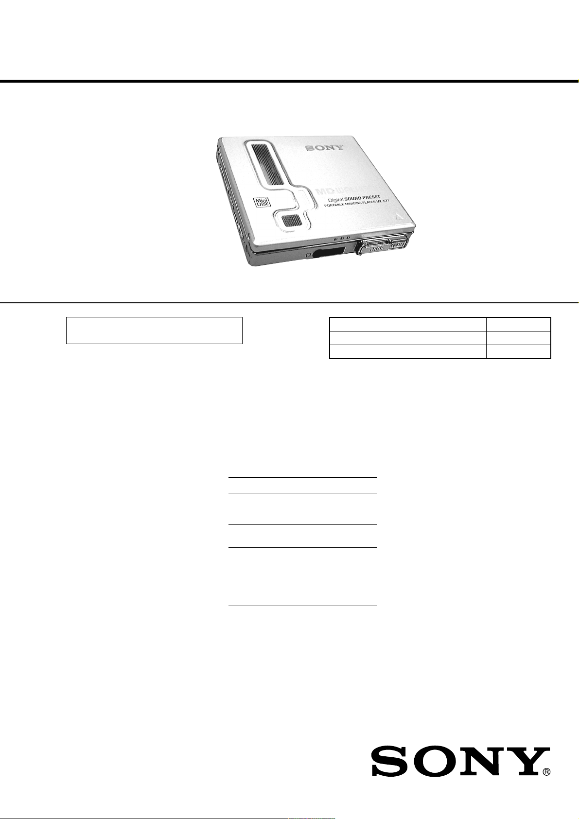
MZ-E77
SERVICE MANUAL
Ver 1.0 2000. 03
Photo: Silver type
US and foreign patents licensed from Dolby
Laboratories Licensing Corporation.
SPECIFICATIONS
E Model
Tourist Model
Model Name Using Similar Mechanism MZ-E90
MD Mechanism Type MT-MZE90-166
Optical Pick-up Mechanism Type LCX-2E
System
Audio playing system
MiniDisc digital audio system
Laser diode properties
Material: GaAlAs
Wavelength: λ = 790 nm
Emission duration: continuous
Laser output: less than 44.6 µW*
* This output is the value measured at a distance
of 200 mm from the objective lens surface on
the optical pick-up block with 7 mm aperture.
Revolutions
600 rpm to 2250 rpm
Error correction
Advanced Cross Interleave Reed Solomon Code
(ACIRC)
Sampling frequency
44.1 kHz
Coding
Adaptive TRansform Acoustic Coding (ATRAC)
Modulation system
EFM (Eight to Fourteen Modulation)
Number of channels
2 stereo channels
1 monaural channel
Frequency response
20 to 20,000 Hz ± 3 dB
Wow and Flutter
Below measurable limit
Outputs
Headphones: stereo mini-jack, maximum output
level 5 mW + 5 mW, load impedance 16 ohms
General
Power requirements
Nickel metal hydride rechargeable battery
NH-14WM (supplied)
One LR6 (size AA) battery (not supplied)
Sony AC Power Adaptor AC-E15L* (not
supplied) connected to the DC IN 1.5V jack
Battery operation time
Battery life*
Batteries
Ni-MH
rechargeable battery
(NH-14WM)
One LR6 (size AA)
alkaline battery
One LR6 (size AA)
alkaline battery
and a Ni-MH
rechargeable
battery
(NH-14WM)
* The battery life may be shorter depending on
operating conditions and the temperature of
the location.
** With a fully charged battery
Playback
Approx. 21 hours**
Approx. 31 hours
Approx. 56 hours**
Dimensions
Approx. 78.3 × 13.9 × 71.4 mm (w/h/d)
1
(3
/8 × 9/16 × 2
parts and controls
Mass
Approx. 85 g (3.0 oz.) the player only
Approx. 128 g (4.5 oz.) incl. a premastered MD
and a nickel metal hydride rechargeable battery
NH-14WM
Supplied accessories
Battery Charger (1)
Rechargeable battery (1)
Rechargeable battery carrying case (1)
Headphones with a remote control (1)
Dry battery case (1)
Carrying pouch (1)
Design and specifications are subject to change
without notice.
7
/8 in.) not including projecting
PORTABLE MINIDISC PLAYER
Page 2

TABLE OF CONTENTS
p
1. SERVICING NOTES............................................... 3
2. GENERAL ................................................................... 4
3. DISASSEMBLY ......................................................... 5
4. TEST MODE.............................................................. 9
5. ELECTRICAL ADJUSTMENTS......................... 14
6. DIAGRAMS
6-1. Block Diagram –RF Section– ......................................... 19
6-2. Block Diagram –SERVO Section – ................................ 21
6-3. Block Diagram –MAIN Section – .................................. 23
6-4. Printed Wiring Board
–MAIN Board (Component Side) – ............................... 25
6-5. Printed Wiring Board
–MAIN Board (Conductor Side) – ................................. 27
6-6. Schematic Diagram –MAIN Board (1/4) – .................... 29
6-7. Schematic Diagram –MAIN Board (2/4) – .................... 31
6-8. Schematic Diagram –MAIN Board (3/4) – .................... 33
6-9. Schematic Diagram –MAIN Board (4/4) – .................... 35
6-10. Printed Wiring Board –SYSTEM Board – ..................... 37
6-11. Schematic Diagram –SYSTEM Board – ........................ 39
6-12. Printed Wiring Board –SW Board – ............................... 41
6-13. Schematic Diagram –SW Board – .................................. 43
6-14. IC Pin Function Description ........................................... 49
Features
• Small body almost the size of a MiniDisc
jacket
Ideal weight and size; fits in your shirt
pocket.
• Personalized sound through Digital
Sound Preset functions
You can store two sets of sound quality
adjustments (made during playback) to
two switches.
• Low power-consumption design enables
extended battery life.
• Simple “One-Touch Eject” function for
easy MiniDisc handling
A single press of the OPEN button causes
the player lid to open and the MiniDisc to
eject.
• Easy-to-operate headphones remote
control with backlit LCD
The LCD displays disc and track
information, playback mode as well as
battery condition. Keep the main unit in
your pocket and operate the MiniDisc
player through the “slim stick” remote
control.
• Shock-resistant memory offsets up to 40
seconds of o
tical read errors.
7. EXPLODED VIEWS................................................ 56
8. ELECTRICAL PARTS LIST ............................... 58
SAFETY-RELATED COMPONENT WARNING!!
COMPONENTS IDENTIFIED BY MARK 0 OR DOTTED
LINE WITH MARK 0 ON THE SCHEMATIC DIA GRAMS
AND IN THE PARTS LIST ARE CRITICAL TO SAFE
OPERATION. REPLACE THESE COMPONENTS WITH
SONY PARTS WHOSE PART NUMBERS APPEAR AS
SHOWN IN THIS MANU AL OR IN SUPPLEMENTS PUBLISHED BY SONY.
– 2 –
Page 3
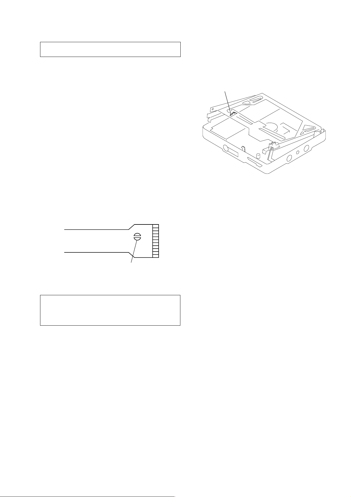
SECTION 1
SW board (S809)
SERVICING NOTES
NOTES ON HANDLING THE OPTICAL PICK-UP
BLOCK OR BASE UNIT
The laser diode in the optical pick-up block may suffer electrostatic break-down because of the potential difference generated
by the charged electrostatic load, etc. on clothing and the human
body.
During repair, pay attention to electrostatic break-down and also
use the procedure in the printed matter which is included in the
repair parts.
The flexible board is easily damaged and should be handled with
care.
NOTES ON LASER DIODE EMISSION CHECK
Never look into the laser diode emission from right above when
checking it for adjustment. It is feared that you will lose your sight.
NOTES ON HANDLING THE OPTICAL PICK-UP BLOCK
(LCX-2E)
The laser diode in the optical pick-up block may suffer electrostatic break-down easily. When handling it, perform soldering
bridge to the laser-tap on the flexible board. Also perform measures against electrostatic break-down sufficiently before the operation. The flexible board is easily damaged and should be handled
with care.
• When repairing this set with the power on, if you remove the
upper panel assy, this set stops working.
In this case, you can work without the set stopping by fastening
the hook of the open/close detect switch (SW board (S809))
with tape.
• This set is designed to perform automatic adjustment for each
adjustment and write its value to EEPROM. Therefore, when
EEPROM (IC802) has been replaced in service, be sure to perform automatic adjustment and write resultant values to the new
EEPROM.
After EEPROM (IC802) is replaced, digital sound preset setting value for display is changed to “00”. Please make sure to
check that digital sound preset setting value for display is “01”.
(Refer to page 14)
laser-tap
OPTICAL PICK-UP FLEXIBLE BOARD
CAUTION
Use of controls or adjustments or performance of procedures
other than those specified herein may result in hazardous radiation exposure.
Flexible Circuit Board Repairing
• Keep the temperature of the soldering iron around 270 ˚C during repairing.
• Do not touch the soldering iron on the same conductor of the
circuit board (within 3 times).
• Be careful not to apply force on the conductor when soldering
or unsoldering.
Notes on chip component replacement
• Never reuse a disconnected chip component.
• Notice that the minus side of a tantalum capacitor may be damaged by heat.
• Replacement of CXD2661GA-2 (IC601) and CXR701080010GA (IC801) used in this set requires a special tool. Therefore, they cannot be replaced.
– 3 –
Page 4
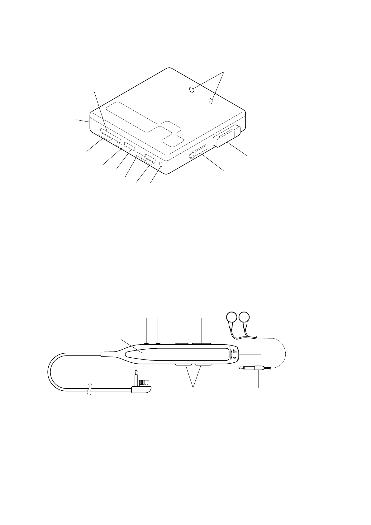
LOCATION OF CONTROLS
8
7
SECTION 2
GENERAL
9
6
5
4
1 OPR indicator
2 HOLD switch
3 >/B and . keys
4 x key
5 DIGITAL SOUND PRESET switch
6 AVLS switch
Remote commander with headphones
3
2
5
1
6
qa
7 Battery cover
8 VOLUME +/– keys
9 External battery terminal
0 OPEN button
qa i (headphone) jack
7
8
0
4
3
1 Headphone
2 B > and . keys
3 VOL +/– keys
4 Display window
5 DISPLAY key
6 PLAYMODE key
7 X key
8 HOLD switch
9 x key
– 4 –
9
21
Page 5
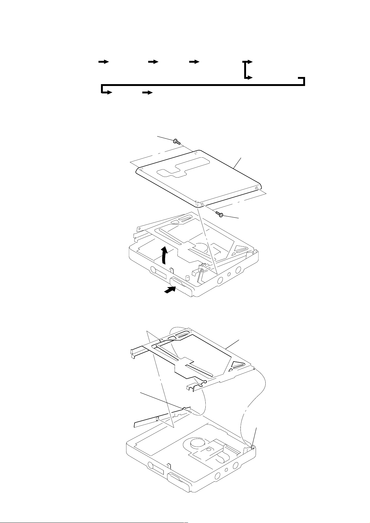
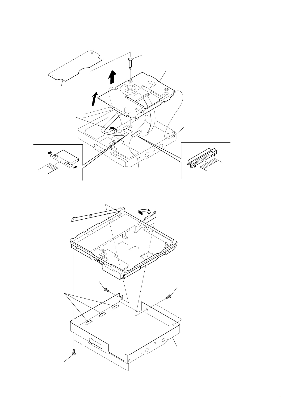
SECTION 3
3 two screws
(MI1.4)
3 two screws
(MI1.4)
4 lid assy, upper
2
1
y
DISASSEMBLY
Note: This set can be disassemble according to the following sequence.
Set
LID ASSY, UPPER
Lid Assy, Upper
strip,
ornamental
Holder Assy
“Chassis Assy, set”, “Case, Battery”,
MAIN board, SW board
Mechanism Deck
(MT-MZE90-166)
Service Assy, OP
(LCX-2E)
Panel Assy Bottom
HOLDER ASSY
3 holder ass
2 shaft
1 shaft
– 5 –
Page 6
MECHANISM DECK
(MT-MZE90-166)
2 screw (MD)
1 seal (moire)
3 claw
8 flexible board (CN551)
PANEL ASSY, BOTTOM
Note: When installing, fit three knobs.
4
6
9 mechanism deck
(MT-MZE90-166)
5 claw
5 claw
7 flexible board (CN501)
knob
1
2 screw
(M1.4)
2 two screws
(MI1.4)
2 two screws
(MI1.4)
3 panel assy, bottom
– 6 –
Page 7
STRIP, ORNAMENTAL
7
strip, ornamental
2 lid, battery case
1 claw
6
5 claw
4 claw
3 claw
9 button (open)
“CHASSIS ASSY, SET”, “CASE, BATTERY”,
MAIN BOARD, SW BOARD
6 case, battery
5 SW board
flexible board
3 Remove the solder
of terminal board (minus).
8 terminal
board (minus)
8 strip, ornamental
9 chassis assy, set
3 Remove the solder
of terminal (plus) assy,
battery.
8 terminal (plus)
assy, battery
7 screw
(MI1.4)
4 MAIN board
2 flexible board
(CN802)
1 four screws
(M1.4)
– 7 –
Page 8
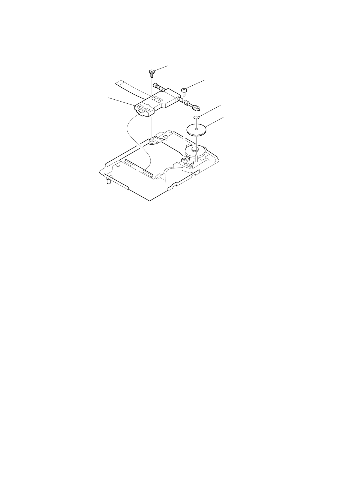
SERVICE ASSY, OP
(LCX-2E)
5 service assy, OP
(LCX-2E)
4 screw
(M1.4)
3 screw
(M1.4)
1 washer
2 gear (SA)
– 8 –
Page 9
SECTION 4
TEST MODE
Outline
• This set provides the Overall adjustment mode that allows CD
and MO discs to be automatically adjusted when in the test mode.
In this overall adjustment mode, the disc is discriminate between
CD and MO, and each adjustment is automatically executed in
order. If a fault is found , the system displays its location. Also,
the manual mode allows each individual adjustment to be automatically adjusted.
• Operation in the test mode is performed with the remote commander. A key having no particular description in the te xt, indicates a remote commander key.
Setting Method of Test Mode
There are two different methods to set the test mode:
1 Short BP801 (TEST) on the SYSTEM board with a solder
bridge (connect pin y; of IC801 to the ground). Then, turn on
the power.
– SYSTEM BOARD (Component Side) –
BP801
(TEST)
Operation in Setting the Test Mode
• When the test mode becomes active, first the display check mode
is selected. (Press the x key once, when the display check mode
is not active)
• Other mode can be selected from the display check mode.
• When the test mode is set, the LCD repeats the following display.
LCD display
All lit
All off
Microprocessor
version
display
• When the X key is pressed and hold down, the display at that
time is held so that display can be checked.
888
004 V1.600
F1SHUF
REC
u
Releasing the Test Mode
For test mode set with the method 1:
Turn off the power and open the solder bridge on BP801 (TEST)
on the SYSTEM board.
Note: Remove the solders completely. Remaining could be shorted with
the chassis, etc.
For test mode set with the method 2:
Turn off the power.
Note: If electrical adjustment (see page 14) has not been finished com-
pletely, always start in the test mode. (The set cannot start in normal mode)
2 In the normal mode, turn on the HOLD switch on the set. While
pressing the x key on the set, press the following remote
commander keys in the following order:
N > t N > t . t . t N > t
. t N > t . t X t X
– 9 –
Page 10
Configuration of Test Mode
[Test Mode $Display Check Mode%]
Press the [VOL +] key
[Manual Mode]
Press the x key
[Servo Mode]
[Audio Mode]
[Power Mode]
[OP Alignment Mode]
Press the . or [VOL --] key
[Overall Adjustment Mode]
Press the x key
press the [DISPLAY] key
[Self-Diagnosis Display Mode]
Press the x key
Press the
for several seconds (about 3 seconds).
[DISPLAY] key
[Key Check Mode]
Quit the key check or open the upper panel
Manual Mode
Mode to adjust or check the operation of the set by function.
Normally, the adjustment in this mode is not executed.
However, the Manual mode is used to clear the memory before
performing automatic adjustments in the Overall Adjustment mode.
• Transition method in Manual Mode
1. Setting the test mode. (See page 9)
2. Press the [VOL +] key activates the manual mode where the
LCD display as shown below.
LCD display
[Major item switching]
N
key
x
>
key
[Medium item switching]
N
>
key
x
key
[Minor item switching]
[VOL +]
[VOL --]
key:100th place of mode number
increase.
key:100th place of mode number
decrease.
[VOL +]
[VOL --]
>
key:10th place of mode number
increase.
key:10th place of mode number
decrease.
N
key: Unit place of mode number
increase.
[Adjusted value variation]
[VOL +]
[VOL --]
key:Increases the
adjusted value
key:Decreases the
adjusted value
[Adjusted value write]
X
key: When adjusted value is
changed:
Adjusted value is written.
When adjusted value is
not changed:
That item is adjusted
automatically.
000 Manual
3. During each test, the optical pick-up moves outward or inward while the
seconds respectively.
4. Each test item is assigned with a 3-digit mode number;
100th place is a major item, 10th place is a medium item, and
unit place is a minor item.
N > or . key is pressed for several
– 10 –
Page 11
5. The display changes a shown below each time the
key is pressed.
• Address & Adjusted Value Display
LCD display
011 C68S01
mode number
address
• Jitter Value & Adjusted Value Display
LCD display
adjusted value
011 OFFJ01
mode number
jitter value
• Block Error Value & Adjusted Value Display
LCD display
adjusted value
011 063B01
block error value
mode number
• ADIP Error Value & Adjusted Value Display
LCD display
adjusted value
[DISPLAY]
Self-Diagnosis Display Mode
• This set uses the self-diagnosis system in which if an error oc-
curs in playback mode, the error is detected by the model control and power control blocks of the microprocessor and information on the cause is stored as history in EEPROM.
By viewing this history in test mode, it helps you to analyze a
fault and determine its location.
1. Setting the test mode. (See page 9)
2. In the display check mode, press the [DISPLAY] key activates
the self-diagnosis display mode where the LCD display as shown
below.
LCD display
000 1st0**
history code
3. Then, each time the N > key is pressed, LCD display descends by one as shown below. Also, the LCD display ascends
by one when the . key is pressed.
1
000 1st0**
error display code
011 059A01
ADIP error value
mode number
• Item Title Display
LCD display
adjusted value
011 LrefPw 01
mode number
item title
However in the power mode (mode number 700’s), only the
item is displayed.
6. Quit the manual mode, and press the
test mode (display check mode).
Overall Adjustment Mode
Mode to adjust the servo automatically in all items.
Normally, automatic adjustment is executed in this mode at the
repair.
For further information, refer to “Section 5 Electrical Adjustments”.
(See page 14)
adjusted value
x key to return to the
000 1st100
000 1st200
000 N 0**
000 N 100
000 N 200
000 N-10**
4. Quit the self-diagnosis display mode, and press the x key to
return to the test mode (display check mode).
000 N-1100
000 N-1200
000 N-20**
000 N-2100
000 N-2200
000 R 0000
1
– 11 –
Page 12
• Description of Indication History
History code number Description
1st 0 The first error
1st 1 Displays “00”
1st 2 Displays “00”
N 0 The last error
N 1 Displays “00”
N 2 Displays “00”
N-1 0 One error before the last.
N-1 1 Displays “00”
N-1 2 Displays “00”
N-2 0 Two errors before the last.
N-2 1 Displays “00”
N-2 2 Displays “00”
REC Total recording time (Displays “0000” in this set)
• Description of Error Indication Codes
Problem Indication code Meaning of code Description
No error 00 No error Normal condition
01
Servo error 02 High temperture High temperture
03 Focus error Forcus could not be applied
04 Spindle error Abnormal lotation of disc
21 Initial low battery Abnormal voltage at initialization
Power error
22 Low battery Momentary interruption detected
23 Low battery NI Momentary interruption detected (NiMH)
24 Low battery AM Momentary interruption detected (AM)
Illegal access target address Attempt to access an abnormal address
was specified
Reset the error display code
After servicing, reset the error display code.
1. Setting the test mode. (See page 9)
2. Press the [DISPLAY] key activates the self-diagnosis display mode.
3. To reset the error display code, press the X key (2 times) when the code is displayed (except “R0000”).
(All the data on the 1st, N, N-1, and N-2 will be reset)
– 12 –
Page 13
Key Check Mode
This set can check if the set and remote commander function normally.
• Setting Method of Key Check Mode
1. Setting the test mode. (See page 9)
2. Press the [DISPLAY] key for several seconds (about 3 seconds) activates the key check mode. (At the last two digits,
AD value of remote commander key line is displayed in hexadecimal)
LCD display
000 **
∗∗: AD value of the remote commander key (hexadecimal 00
to FF)
3. When each key on the set and on remote commander is pressed,
its name is displayed on the LCD. (The operated position is
displayed for 4 seconds after the slide switch is operated. If
any other key is pressed during this display, the LCD switches
to its name display.)
Example1: When >/N key on the set is pressed:
LCD display
000 FF **
∗∗: AD value of the remote commander key (hexadecimal 00
to FF)
Example2: When N > key on the remote commander is
pressed:
LCD display
000 rPLAY **
∗∗: AD value of the remote commander key (hexadecimal 00
to FF)
4. When all the keys on the set and on the remote commander are
considered as OK, the following displays are shown for 4 seconds.
(The key pressed to enter the Key Check mode has been check ed
even if it is not pressed in this mode)
Example1: When the keys on the set are considered as OK:
LCD display
000 SET OK **
∗∗: AD value of the remote commander key (hexadecimal 00
to FF)
Example2: When the keys on the remote commander are con-
sidered as OK:
LCD display
000 RMC OK **
∗∗: AD value of the remote commander key (hexadecimal 00
to FF)
5. When all the key have been checked or when the top panel is
opened during this checking, the system terminates the Key
Check mode and return to the test mode (display check mode).
– 13 –
Page 14
SECTION 5
ELECTRICAL ADJUSTMENTS
Outline
• In this set, automatic adjustment of CD and MO can be performed by entering the test mode. (See page 9)
However , before starting automatic adjustment, the memory clear
and power adjustment must be performed in the manual mode.
• A key having no particular description in the text, indicates a
remote commander key.
Precautions for Adjustment
1. Adjustment must be done in the test mode only.
After adjusting, release the test mode.
2. Use the following tools and measuring instruments.
• Test CD disc TDYS-1
(Part No. : 4-963-646-01)
• Recorded MO disc PTDM-1
(Part No. : J-2501-054-A)
Available SONY MO disc (recorded)
• Digital voltmeter
3. Unless specified otherwise, supply DC 1.2V from the DC IN
jack.
4. Switch position
AVLS switch ................................................ NORM
DIGITAL SOUND PRESET switch ........... OFF
HOLD switch ............................................... OFF
Adjustment Sequence
Adjustment must be done with the following steps.
1. NV Reset (Memory clear)
r
2. Digital Sound Preset Setting Manual Mode
r
3. Power Supply Manual Adjustment
r
4. CD Overall Adjustment
r Overall Mode
5. MO Overall Adjustment
NV Reset
• Setting method of NV reset
1. Select the manual mode of test mode, and set mode number 021NV Reset. (See page 10)
LCD display
021 ResNV
2. Press the X key.
LCD display
021 ResOK?
3. Press the X key once more.
LCD display
021 Res***
NV reset (after several seconds)
021 Reset!
4. Press the x key to quit the manual mode, and activate
the test mode.
Digital Sound Preset Setting
1. Select the manual mode of the test mode, and set the item
number 045. (See page 10)
LCD display
045 D.S.P **
∗∗: Adjustment value of digital sound preset set up.
2. Adjust [VOL +] key so that the adjustment value becomes
01.
LCD display
045 XXXS01
3. Press the X key to write the adjusted value.
Power Supply Manual Adjustment
• Adjustment sequence
Adjustment must be done with the following steps.
1. Vc PWM Duty (L) adjustment (item number: 762)
r
2. Vrem PWM Duty (L) adjsutment (item number: 764)
r
3. Vc PWM Duty (H) adjustment (item number: 765)
r
4. Vrem PWM Duty (H) adjustment (item number: 766)
– 14 –
Page 15
• Adjustment method of Vc PWM Duty (L)
(item number: 762)
1. Select the manual mode of the test mode, and set the item num-
ber 762. (See page 10)
LCD display
• Adjustment method of Vrem PWM Duty (H)
(item number: 766)
1. Select the manual mode of the test mode, and set the item
number 766. (See page 10)
LCD display
762 Vc1PWM
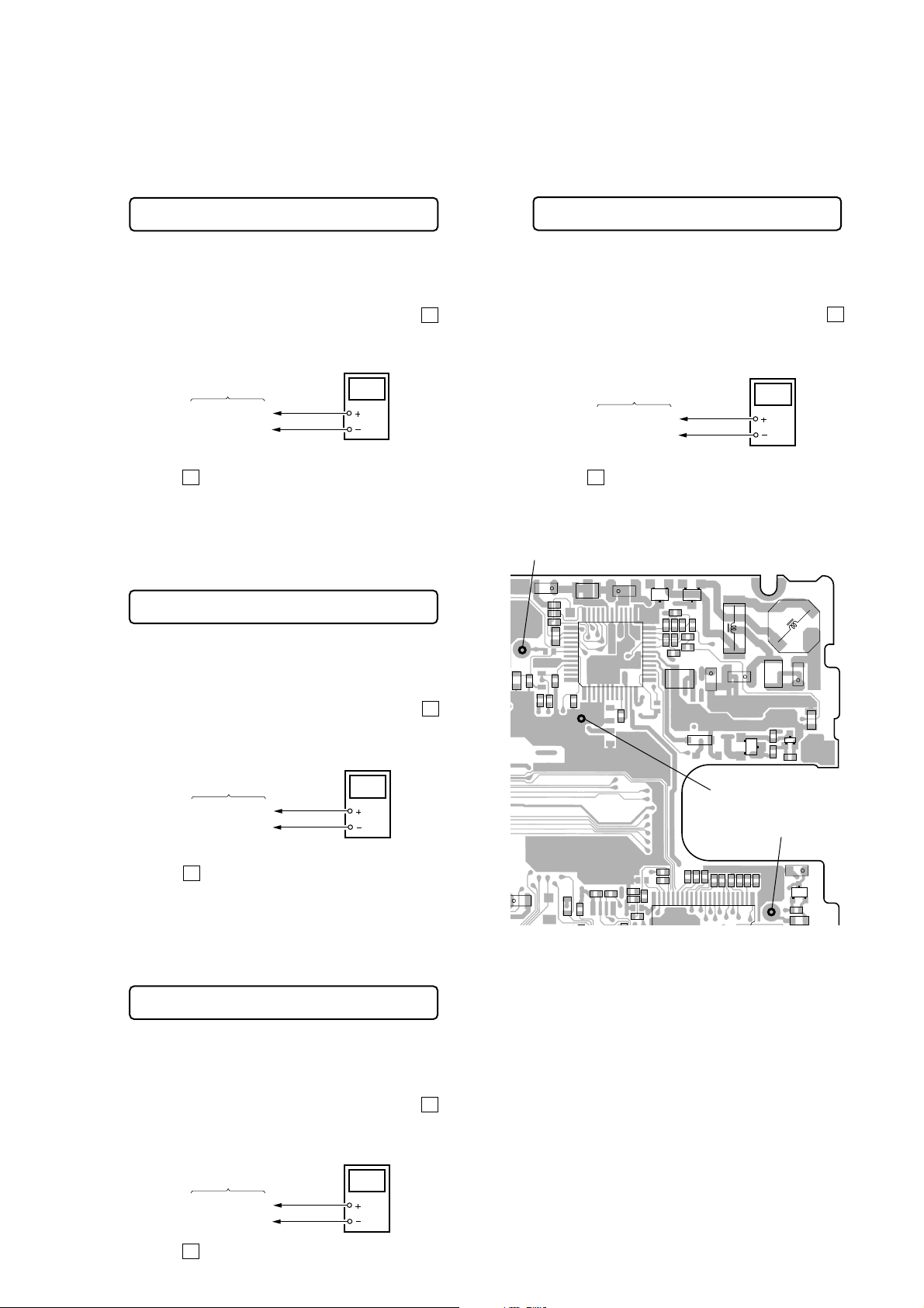
2. Connect a digital voltmeter to the TP901 (VC) on the MAIN
board, and adjust
(voltage down) so that the voltage becomes 2.32 V.
[VOL +] key (voltage up) or [VOL --] key
+0.005
–0.01
Proceed to the next adjustment without pressing the X key if
voltage is already adjusted.
digital
voltmeter
MAIN board
TP901 (VC)
TP912 (GND)
3. Press the X key to write the adjusted value.
• Adjustment method of Vrem PWM Duty (L)
(item number: 764)
1. Select the manual mode of the test mode, and set the item number 764. (See page 10)
LCD display
764 Vr1Vc1
2. Connect a digital voltmeter to the TP903 (VR) on the MAIN
board, and adjust
(voltage down) so that the voltage becomes 2.25 V.
Proceed to the next adjustment without pressing the X key if
voltage is already adjusted.
3. Press the
• Adjustment method of Vc PWM Duty (H)
(item number: 765)
1. Select the manual mode of the test mode, and set the item number 765. (See page 10)
LCD display
[VOL +] key (voltage up) or [VOL --] key
digital
voltmeter
MAIN board
TP903 (VC)
TP912 (GND)
X key to write the adjusted value.
+0.005
–0.01
766 VrhVch
2. Connect a digital voltmeter to the TP903 (VR) on the MAIN
board, and adjust
(voltage down) so that the voltage becomes 2.6 ± 0.015 V.
Proceed to the next adjustment without pressing the X key if
voltage is already adjusted.
3. Press the X key to write the adjusted value.
Adjustment and Connection Location:
– MAIN Board (Component side) –
TP901 (VC)
+
C917
CN501
20
1
C557
L551
C902
L903
C918
R922
36 25
R921
37
R920
R918
+
C553
48
C915
C916
112
R943
C908
R940
C855
R551
R809
CN802
1
[VOL +] key (voltage up) or [VOL --] key
digital
voltmeter
MAIN board
TP903 (VC)
TP912 (GND)
A
+
IC901
R552 C552
85
IC552
C901
24
13
R936
R505
R517
C527
R516
C551
R630
C619
A
D902
D901
K
K
R941
R903
C905
R902
R909
L902
C906
R904
R905
R910
R942
+
C911
D903
AK
C903
L905
TP912 (GND)
R518
C507
C506
C530
22 1
23 44
C505
C504
C503
C502
R501
IC501
+
L904
Q901
R937R938
G
D
S
TP903 (VR)
R502
C501
R503
Q902
BCE
R944
L901
C904
+
C907
+
C529
C
Q501
B
E
R519
R521
C519
765 VchPWM
2. Connect a digital voltmeter to the TP901 (VC) on the MAIN
board, and adjust
(voltage down) so that the voltage becomes 2.75 ± 0.015 V.
Proceed to the next adjustment without pressing the X key if
voltage is already adjusted.
3. Press the
[VOL +] key (voltage up) or [VOL --] key
digital
voltmeter
MAIN board
TP901 (VC)
TP912 (GND)
X key to write the adjusted value.
– 15 –
Page 16

Overall Adjustment Mode
• Configuration of overall adjustment
N >
key . key
Overall adjustment mode
(Title display)
6. Insert MO disc in the set, and press the
Overall MO Adjustment mode. Automatic adjustments are
made.
LCD display
N > key to set the
XXX MO RUN
CD overall
adjusting
All item
OK
x
key
CD overall
x
key
x
key
x
key
adjustment
MO overall
adjusting
MO overall
adjustment
OK
OK
N >
NG item exists
or
x
key
CD overall
adjustment
NG
key
NG item exists
or
x
key
MO overall
adjustment
NG
[Test mode $display check mode%]
Note: Adjust the CD first, when performing adjustment.
• Adjustment Method of Overall CD and MO Adjustment
Mode
1. Setting the test mode. (See page 9)
2. Press the [VOL --] key activates the overall adjustment mode.
LCD display
000 AssyFF
XXX: Item number for which an adjustment is being executed.
7. If NG in the overall MO adjustments, return to Reset NV and
perform the adjustment again.
LCD display
000 *** NG
∗∗∗: NG item number.
8. If OK through the overall MO adjustments, press the x key
to return to the test mode and terminate the Overall Adjustment
mode.
LCD display
000 MO OK
• Overall CD and MO adjustment items
1. Overall CD adjustment items
Item No. Descr iption
312
313 CD electrical offset adjustment
314
328 CD TWPP gain adjustment
321 CD tracking error gain adjustment
323
332
336 CD ABCD level adjustment
344 CD focus gain adjustment
345 CD tracking gain adjustment
521
522
341 CD focus bias adjustment
tracking error
CD
CD two-axis sensitivity adjustment
offset adjustment
3. Insert CD disc in the set, and press the . key to set the
Overall CD Adjustment mode . Automatic adjustments are made.
LCD display
XXX CD RUN
XXX: Item number for which an adjustment is being executed.
4. If NG in the overall CD adjustments, return to Reset NV and
perform the adjustment again.
LCD display
000 *** NG
∗∗∗: NG item number.
5. If OK through the overall CD adjustments, then perform overall MO adjustments.
LCD display
000 CD OK
– 16 –
Page 17

2. Overall MO adjustment items
Item No. Descr iption
112
113
114
118
221 Low reflective CD tracking error gain adjustment
223
232
236 Low reflective CD ABCD level adjustment
244 Low reflective CD focus gain adjustment
245 Low reflective CD tracking gain adjustment
121 MO tracking error gain adjustment
122 MO tracking error offset adjustment
134 MO TWPP gain adjustment
131
132
136 MO ABCD level adjustment
144 MO focus gain adjustment
145 MO tracking gain adjustment
141 MO focus bias adjustment
MO electrical offset adjustment
Low reflective CD tracking error offset adjustment
MO double speed read TWPP offset adjustment
– 17 –
Page 18

6-1. BLOCK DIAGRAM – RF Section –
MZ-E77
SECTION 6
DIAGRAMS
OPTICAL PICK-UP BLOCK
JX JY JX
IX IY
IX
CD
A
B
F
MON
(LCX-2E)
IY
IX
JX
JY
A
B
C
D
LD
AVCC
MAIN BOARD (1/3 )
RF AMP,FOCUS/TRACKING ERROR AMP
CN501
VREF
6
6
IY
9
9
IX
10
10
JX
14
14
JY
15
15
A
16
16
B
17
17
C
7
7
D
8
8
MON
18
18
5
5
LD-A
12
LD-K
13
AVCC
20
S0
11
S0
S1
S1
19
AUTOMATIC
POWER
12
CONTROL
13
20
11
19
AVCC AVCC
L501
Q501
L502
4
VREF
IY
8
IX
9
JX
10
JY
11
A
12
B
14
C
5
D
6
A-C
13
D-C
7
PD-NI
18
PD-O
20
22
DVDD
40
AVCC
RF,AMP,
FOCUS
ERROR,
TRACKING
ERROR
TPP/WPP
APC
IC501
PEAK
/BOTM
RF OUT
PEAK
BOTM
ABCD
ADIP IN
ADIP
PD-NI
OFTRK
XRST
SBUS
SCK
S MON
DIGITAL SIGNAL PROCESSOR,
DIGITAL SERVO SIGNAL PROCESSOR,
EFM/ACIRC ENCODER/DECODER,
SHOCK PROOF MEMORY CONTROLLER,
16M BIT D-RAM
IC601(1/2)
CN801
(1/3)
24
RFI
33
29
28
41
FE
42
TE
1
44
21
19
31
VC
26
25
23
24
43
78
84
85
86
87
96
99
106
89
12
4
PEAK
BOTM
ABCD
FE
TE
ADIP
APCREF
VC
MNT2
XRST
AOUT L
AOUT R
AVD1
AVD2
VDIOSC
VDI01
VDI02
VDI03
VDD RAM
VDD RAM
MNT3
SWDT
SCLK
XLAT
SRDT
SENS
SQSY
XINT
CS DSP
27
76
92
18
53
100
125
144
146
5
6
7
8
10
11
13
16
32
AVCC
L601
7
5
31
25
45
17
43
19
44
41
13
29
11
35
40
48
16
33
42
L IN
R IN
FOK
SDO0
SCK0
XLAT
SDI0
SENSE
SQSY
XINT
XCS DSP
OFTRK
VREF MON
SSB DATA
SSB CLK
S MON
PS S0
PD S1
XICRST
B
(Page 23)
TRK+
2
2
TRACKING
COIL
2-AXIS
DEVICE
FOCUS
COIL
05
TRK-
1
1
FCS+
4
4
FCS-
3
3
TRK+
TRK-
FCS+
FCS-
A
(Page 21)
• SIGNAL PATH
: PLAYBACK
– 19 – – 20 –
Page 19

MZ-E77
6-2. BLOCK DIAGRAM – SERVO Section –
M902
(SLED)
MM
M901
(SPINDLE)
5
7
6
8
1
2
3
4
SLED1+
SLED1-
SLED2+
SLED2-
CLVN
CLVU
CLVV
CLVW
MAIN BOARD (2/3)
TRK+
TRK-
A
(Page 19)
CN551
5
7
6
8
1
2
3
4
FCS+
FCS-
UNREG
AVCC
30
29
33
32
11
12
26
28
37
38
39
40
46
47
44
43
42
7
4
8
5
9
FO3
VM34
VM3
RO3
FO1
VM1
VM12
RO1
FO2
VM2
RO2
FO4
RO4
COM
CPW1
CPV1
CPU1
UO
VMU
VO
VMVW
WO
SLED
VOLTAGE MONITOR
IC552
5
6
3
2
FOCUS/TRACKING COIL DRIVE,
SPINDLES/SLED MOTOR DRIVE
PRE
DRIVER
PRE
DRIVER
PRE
DRIVER
PRE
DRIVER
PRE
DRIVER
IC551
7
1
HI-BRIDGE
CONTROL
HI-BRIDGE
CONTROL
HI-BRIDGE
CONTROL
HI-BRIDGE
CONTROL
3 PHASE
CONTROL
BIAS
RI3
RI1
RI2
PWM24
RI4
COW0
COV0
COU0
W1
PWM1
DIGITAL SIGNAL PROCESSOR,
DIGITAL SERVO SIGNAL PROCESSOR,
EFM/ACIRC ENCODER/DECODER,
SHOCK PROOF MEMORY CONTROLLER,
16M BIT D-RAM
IC601(2/2)
VDCO
VDC1
VDC2
SLCV
139
SLCU
138
FI3
21
22
FI1
16
15
13
FI2
14
25
FI4
23
24
34
35
36
48
V1
1
U1
2
3
OE
17
110
109
111
112
134
133
141
135
140
132
131
130
FFCLR
TFDR
TRDR
FFDR
FRDR
SLDV
SLDU
SLVS
SLDW
SLCW
SPCW
SPCV
SPCU
D
(Page 24)
VDC3
VDC4
VDC5
DAVDDL
DAVDDR
OSCI
OSCO
SPVS
SPDU
SPDV
SPDW
108
136
124
127
128
129
VREG
1
36
37
68
VLD
25
26
19
20
X601
22.5792MHz
SPINDLE SERVO DRIVE SWITCH
SPINDLE SERVO DRIVE SWITCH
IC504
1
7
6
3
IC505
1
7
6
3
2
5
2
5
CN801
(2/3)
21
27
30
26
28
32
SPDL START SW
SLD 1 MON
CLV W
CLV V
CLV U
SPDL PWM
C
(Page 23)
– 21 –
18
VC
VG VG
20
05
– 22 –
Page 20

6-3. BLOCK DIAGRAM – MAIN Section –
MZ-E77
B
(Page 20)
C
(Page 22)
L IN
R IN
FOK
SDO0
SCK0
XLAT
SDI0
SENSE
SQSY
XINT
XCS DSP
OFTRK
VREF MON
SSB DATA
SSB CLK
S MON
PD S0
PD S1
XICRST
SPDL START SW
SLD 1 MON
CLV W
CLV V
CLV U
SPDL PWM
SYSTEM BOARD MAIN BOARD (3/3 )
CN803
(1/2)
7
5
UNREG
AVCC
REFERENCE
VOLTAGE
SWITCHING
Q301
EEPROM
IC802
4
DI
3
DO
2
SK
1
XCS
119
31
25
45
17
43
19
44
41
13
29
11
35
40
48
16
33
42
21
27
30
26
28
32
X801
16.9344MHz
XCS NV
FOK
52
SO0
12
SCK0
13
8
XLAT
SI0
11
6
SENSE
SQSY
53
55
XINT
XCS DSP
9
2
OFTRK
82
VREF MON
SSB DATA
102
103
SSB CLK
79
S MON
36
PD S0
38
PDS1
68
XICRST
49
SPDL START SW
SLD 1 MON
35
26
CLV W
25
CLV V
24
CLV U
67
SPDL PWM
45
XTAL
46
EXTAL
IN L
22
IN R
21
+B
1
VCC
20
VREF IN
13
SYSTEM CONTROL
HEADPHONE AMP
IC301
BEEP OUT A
BEEP OUT A
BEEP
IC801
OPEN CLOSE SW
REG CTL PWM
OUT L
OUT R
STB
MUTE
MUTE
XHP STB
BEEP
RMC DTCK
SET KEY 2
XAVLS
SET KEY 1
WK DET
OPR LED
HOLD SW
RMC KEY
VBKAN
VC PWM
VB MON
VRM PWM
SERON
SLEEP
FFCLR
XRST
VDD
VDD
VDD
AVDD
VDD
AVREF
VRM MON
CN803
2
4
24
23
15
18
17
117
23
18
19
87
115
86
83
84
69
73
85
78
66
80
65
64
58
40
39
43
16
47
74
93
105
92
89
(2/2)
UNREG
AVCC
L OUT
1
R OUT
3
RMC DATA
38
22
24
SET KEY
14
18
OPEN/CLOSE
9
OPR LED
20
HOLD SW
37
RMC KEY
39
10
VC PWM
50
VRM PWM
49
REG CTL PWM
46
SERON
47
36
15
34
12
DBB
AVLS
XWK1
VSTB
SLEEP
FFCLR
XRST
VDD
38
22
24
14
18
20
37
39
10
50
49
46
47
36
15
34
12
CN801
(3/3)
1
3
9
NOISE
FILTER
NOISE
FILTER
UNREG
VDD
VREG
VLD
CN802 CN804
POWER CONTROL
34
XWK2
35
XWK1
39
VRMS
33
XWK3
38
VSTB
32
XWK4
22
INM1
RF1
24
23
RF2
20
INM2
43
CLK
15
SERON
36
SLEEP
37
FFCLR
40
XRST
30
VC
45
VREF
21
DTC
1
2
3
4
5
OPEN/CLOSE
6
7
HOLD SW
8
IC901
SWVG
VR OUT
VC ON
VC IN
VREG
DBB
DBB1
AVLS
SET KEY
XWK1
OPR LED
VG
VR
L2
VB
L1
FB
VLD
19
17
12
25
26
44
28
29
31
9
10
11
VDD
SW BOARD
DIGITAL SOUND PRESET
9
8
7
6
5
4
3
2
D903
L905
L903
AVCC
L904
D902
L902
L901
D901
OPR
VG
RCH
LCH
GND
GND
KEY
DATA
S806
OFF 1 2
D801
S808
HOLD
OFF HOLD
B+ SWITCH
Q901, 902
J301
(HEADPHONE)
i
S809
(OPEN/CLOSE)
S807
AVLS
NORM LIMIT
(BATTERY CASE)
• SIGNAL PATH
S801 – 805
RECHARGEABLE
BATTERY
(NICKEL-METAL)
NH-14WN
1.2V 1400mAh
DRY BATTERY
SIZE "AA"
(IEC DESIGNATION R6)
1PC. 1.5V
: PLAYBACK
S801
x
S802
> / N
S803
.
S804
VOLUME
-
-
S805
VOLUME
+
DC IN 1.5V
–
+
(Page 22)
05
D
– 23 – – 24 –
Page 21

MZ-E77
e
6-4. PRINTED WIRING BOARD – MAIN Board (Component Side) –
• Semiconductor
Location
Ref. No. Location
D101 J-5
D201 I-4
D601 H-8
D855 I-6
D901 A-9
D902 A-8
D903 D-9
IC501 G-9
IC504 I-5
IC505 I-6
IC551 G-4
IC552 G-7
IC601 J-9
IC901 B-7
Q501 F-11
Q901 D-10
Q902 D-11
Note on Printed Wiring Board:
• Y : parts extracted from the conductor side.
f
•
• b : Pattern from the side which enables seeing.
(The other layers' patterns are not indicated.)
Caution:
Pattern face side: Parts on the pattern face side seen from
(Conductor Side) the pattern face are indicated.
Parts face side: Parts on the parts face side seen from
(Component Side) the parts face are indicated.
• Main board is four-layer printed board.
• Lead Layouts
: internal component.
However, the patterns of layers 2 and 3 have not been included in this diagrams.
IC601 is not replaceable
*
surfac
1 2 3 4 5 6 7 8 9 10 11 12 13
MAIN BOARD
A
+
B
+
C952
C
L554
D
MOTOR FLEXIBLE
BOARD
1-675-668-
E
M901
(SPINDLE)
F
M902
(SLED)
1
2
3
4
5
M
6
7
8
G
12
RECHARGEABLE
BATTERY
(NICKEL-METAL)
NH-14WM
1.2V 1400mAh
H
(Page 42)
I
J
A
SW
BOARD
CN804
SWITCH FLEXIBLE
BOARD
1-675-336-
11
K
18
+
1
L552
C555
+
12
L553
C351
R
COM
(COMPONENT SIDE)
C953
+
C556
R555
CN551
R822
C559
R554
IC551
R821
C954
C554
48 37
13 24
D201
AK
L501
C518
R556
L
C558
GND
C917
CN501
20
1
R553
C557
36
25
C561
85
14
R828
KA
D101
C854
KEY
L551
IC504
FB802
C853
DATA
TP901
(VC)
R918
+
C553
C521
85
C522
IC505
14
54
KK
D855
KAK
123
C851
VDD
C916
R819
R817
FB801
C902
R818
R943
+
C918
R922
R921
C908
CN802
R816
L903
36 25
37
R920
48
C915
112
R940
TP912
(GND)
C855
R551
R809
1
9
L502
25
CN801
1
+
C901
IC901
R936
R552 C552
85
IC552
14
RB551
+
C524
26
50
C551
A
D902
K
R902
24
R904
R942
13
R518
C530
R505
R517
C527
22 1
R516
R630
C619
23 44
RB552
C517
D601
C526
AK
C619
111112 108
114116 113
117118 115
120121 119
123124 122
127126 125
129130 128
132133 131
135137 134
R620
C101
C201
138139 136
141142
+
+
C104
C204
A
D901
K
R941
R903
C905
R909
C906
R905
R910
L905
D903
AK
C507
C506
IC501
C516
C615
R615
R515
C515
101
105
107
102
104
106
140
23
1 11121518 25262832361473839
6 10131619
4
5 8 9 141720
7
X601
+
C505
C513
C511
C616
L902
C911
C504
C503
C509
C510
IC601
24 23 27 31 34 35
21 22 29 30 33 143
R603
C903
PICK-UP BLOCK
C502
R501
*
R105
+
G
S
C618
Q901
OPTICAL
(LCX-2E)
C501
C614
R612
R614
R610
C607
R205
D
R502
145747577798081838486878990919395949899
146 67 69
144 40 41
C605
L904
R937R938
TP903
(VR)
R503
C508
C620
R611
R609
72
70737678828588929697100103109110 71
68 66 65
64 63 62
59 60 61
56 57 58
53 55 54
50 51 52
47 48 49
46 45 44
37 42 43
C606
+
R504
C613
R608
Q902
BCE
R944
R607
R602
C529
L901
B
R519
C
Q501
R521
C519
C904
+
R601
+
C603
C604C608
R604
C612
E
L601
C610
+
C907
C611
R606
R605
C609
+
1-677-152-
(BATTERY CASE)
(IEC DESIGNATION R6)
+
11
(11)
DRY BATTERY
SIZE “AA”
1PC. 1.5V
DC IN 1.5V
–
+
Lead layout of conv entional IC CSP (chip size package)
05
– 25 –
J301
i
(HEADPHONE)
B
(Page 38)
SYSTEM
BOARD
CN803
– 26 –
Page 22

6-5. PRINTED WIRING BOARD – MAIN Board (Conductor Side) –
MAIN BOARD
(CONDUCTOR SIDE)
MZ-E77
12345678910111213
A
B
C
D
E
F
G
H
I
J
05
1-677-152-
11
(11)
K
– 27 – – 28 –
Page 23

MZ-E77
6-6. SCHEMATIC DIAGRAM – MAIN Board (1/4) – • See page 45 for Waveforms. • See page 46 for IC Block Diagram.
(Page 31)
(Page 35)
(Page 35)
Note on Schematic Diagram:
• All capacitors are in µF unless otherwise noted. pF: µµF
50 WV or less are not indicated except for electrolytics
and tantalums.
• All resistors are in Ω and 1/
specified.
• % : indicates tolerance.
• A : B+ Line.
• Power voltage is dc 1.5V and fed with regulated dc po wer
supply from battery terminal.
4
W or less unless otherwise
(Page 34)
• Voltages and wav eforms are dc with respect to ground in
playback mode.
no mark : PLAYBACK
• Voltages are taken with a VOM (Input impedance 10 MΩ).
Voltage variations may be noted due to normal production tolerances.
• Waveforms are taken with a oscilloscope.
Voltage variations may be noted due to normal production tolerances.
– 29 – – 30 –
• Circled numbers refer to waveforms.
• Signal path.
E : PLAYBACK
Note: The components identified by mark 0 or dotted line
with mark 0 are critical for safety.
Replace only with part number specified.
Page 24

6-7. SCHEMATIC DIAGRAM – MAIN Board (2/4) –• See page 45 for Waveforms.
MZ-E77
(Page 43)
(Page 30)
(Page 34)
(Page 34)
Note on Schematic Diagram:
• All capacitors are in µF unless otherwise noted. pF: µµF
50 WV or less are not indicated except for electrolytics
and tantalums.
• All resistors are in Ω and 1/
specified.
• % : indicates tolerance.
f
•
• C : panel designation.
: internal component.
4
W or less unless otherwise
– 31 –
(Page 36)
• A : B+ Line.
• Power voltage is dc 1.5V and fed with regulated dc po wer
supply from battery terminal.
• Voltages and wav eforms are dc with respect to ground in
playback mode.
no mark : PLAYBACK
: Impossible to measure
∗
• Voltages are taken with a VOM (Input impedance 10 MΩ).
Voltage variations may be noted due to normal production tolerances.
• Waveforms are taken with a oscilloscope.
Voltage variations may be noted due to normal production tolerances.
• Circled numbers refer to waveforms.
– 32 –
• Signal path.
E : PLAYBACK
IC601 is not replaceable
*
• The voltage and waveform of CSP (chip size package)
cannot be measured, because its lead layout is different
form that of conventional IC.
Page 25

MZ-E77
6-8. SCHEMATIC DIAGRAM – MAIN Board (3/4) –• See page 45 for Waveform. • See page 48 for IC Block Diagram.
Note on Schematic Diagram:
• All capacitors are in µF unless otherwise noted. pF: µµF
50 WV or less are not indicated except for electrolytics
and tantalums.
• All resistors are in Ω and 1/
specified.
• % : indicates tolerance.
• A : B+ Line.
• Power voltage is dc 1.5V and f ed with regulated dc power
supply from battery terminal.
• Voltages and waveform are dc with respect to ground in
playback mode.
no mark : PLAYBACK
• Voltages are taken with a VOM (Input impedance 10 MΩ).
Voltage variations may be noted due to normal production tolerances.
• Waveform is taken with a oscilloscope.
Voltage variations may be noted due to normal production tolerances.
• Circled number refers to waveform.
4
W or less unless otherwise
(Page 29)
(Page 31)
(Page 31)
(Page 35)
– 33 – – 34 –
Page 26

6-9. SCHEMATIC DIAGRAM – MAIN Board (4/4) –• See page 45 for Waveforms. • See page 47 for IC Block Diagram.
MZ-E77
(Page 29)
(Page 31)
(Page 34)
(Page 39)
(Page 30)
– 35 –
Note on Schematic Diagram:
• All capacitors are in µF unless otherwise noted. pF: µµF
50 WV or less are not indicated except for electrolytics
and tantalums.
• All resistors are in Ω and 1/
specified.
• C : panel designation.
• A : B+ Line.
• Total current is measured with MD installed.
4
W or less unless otherwise
• Power voltage is dc 1.5V and fed with regulated dc po wer
supply from battery terminal.
• Voltages and wav eforms are dc with respect to ground in
playback mode.
no mark : PLAYBACK
• Voltages are taken with a VOM (Input impedance 10 MΩ).
Voltage variations may be noted due to normal production tolerances.
– 36 –
• Waveforms are taken with a oscilloscope.
Voltage variations may be noted due to normal production tolerances.
• Circled numbers refer to waveforms.
• Signal path.
E : PLAYBACK
Page 27

MZ-E77
e
6-10. PRINTED WIRING BOARD – SYSTEM Board –
• Semiconductor
Location
Ref. No. Location
IC301 F-3
IC801 F-6
IC802 F-8
Q301 G-3
A
B
C
1 2 3 4 5 6 7 8
SYSTEM BOARD
(COMPONENT SIDE)
Note on Printed Wiring Board:
• Y : parts extracted from the conductor side.
f
•
• b : Pattern from the side which enables seeing.
(The other layers' patterns are not indicated.)
Caution:
Pattern face side: Parts on the pattern face side seen from
(Conductor Side) the pattern face are indicated.
Parts face side: Parts on the parts face side seen from
(Component Side) the parts face are indicated.
• System board is four-layer printed board.
• Lead Layouts
Lead layout of conv entional IC CSP (chip size package)
: internal component.
However, the patterns of layers 2 and 3 have not been included in this diagrams.
IC801 is not replaceable
*
surfac
D
E
F
G
BP801
(TEST)
1-677-232-
11
(11)
R806
1
SYSTEM BOARD
C102
R103
R203
C202
(CONDUCTOR SIDE)
R204
C305
7
C306
+
12
+
+
C304
+
Q301
C203
BCE
IC301
R302
R303
C103
16
1813
C303
R104
24
19
C302
+
R201
R202
R301
CN803
R101
R102
25
C301
B
MAIN
05
BOARD
CN801
50
R801
R802
C802
R826
26
(Page 26)
C803
R810
93 92 91 61 55 56
96 95 94 52 53 54
99 98 97 49 50 51
102 101 100 46 47 48
105 104 103 43 45 44
108 107 106 40 41 42
109 110 111 37 38 39
113 114 112 34 35 36
117 116 115 4 7 10 13 16 19 22
C809
119 118 2 6 8 11 14 17 21 23 26 28 31
120 1 3 5 9 12 15 18 20 24 25 29 30
C804
R804
R803
83 81 78 74 72 69 6488 87 86 63 60 58
84 80 77 75 71 68 6590 89 85 62 59 57
82 79 76 73 70 67 66
C811
IC801
C806
C807
*
27 32 33
R808
R807
R827
41
IC802
58
R815
C808
X801
1-677-232-
1-677-232-
11
11
(11)
(11)
– 37 – – 38 –
Page 28

6-11. SCHEMATIC DIAGRAM – SYSTEM Board – • See page 45 for Waveforms. • See page 48 for IC Block Diagram.
MZ-E77
(Page 36)
Note on Schematic Diagram:
• All capacitors are in µF unless otherwise noted. pF: µµF
50 WV or less are not indicated except for electrolytics
and tantalums.
• All resistors are in Ω and 1/
specified.
f
•
• A : B+ Line.
• Power voltage is dc 1.5V and fed with regulated dc po wer
• Voltages and wav eforms are dc with respect to ground in
• Voltages are taken with a VOM (Input impedance 10 MΩ).
• Waveforms are taken with a oscilloscope.
• Circled numbers refer to waveforms.
• Signal path.
: internal component.
supply from battery terminal.
playback mode.
no mark : PLAYBACK
Voltage variations may be noted due to normal production tolerances.
Voltage variations may be noted due to normal production tolerances.
E : PLAYBACK
: Impossible to measure
∗
4
W or less unless otherwise
– 39 – – 40 –
IC801 is not replaceable
*
• The voltage and waveform of CSP (chip size package)
cannot be measured, because its lead layout is different
form that of conventional IC.
Page 29

MZ-E77
6-12. PRINTED WIRING BOARD – SW Board –
1 2 3 4 5 6 7 8 9 10
A
B
C
D
SW BOARD
S804
VOLUME –
SW BOARD
R813
(COMPONENT SIDE)
(CONDUCTOR SIDE)
S807
AVLS
NORM , LIMIT
R814
S805
VOLUME +
S806
DIGITAL SOUND PRESET
OFF , 1 , 2
S801
x
S809
(OPEN/CLOSE)
S803
.
R812
SWITCH FLEXIBLE
BOARD
1-675-336-
S808
HOLD
OFF , HOLD
>/N
11
R811
1-677-151-
S802
CN804
91
1-677-151-
D801
OPR
(Page 25)
A
11
(11)
MAIN
BOARD
CN802
11
(11)
05
Note on Printed Wiring Board:
• Y : parts extracted from the conductor side.
z
•
(The other layers' patterns are not indicated.)
Caution:
Pattern face side: Parts on the pattern face side seen from
(Conductor Side) the pattern face are indicated.
Parts face side: Parts on the parts face side seen from
(Component Side) the parts face are indicated.
: Through hole.
– 41 –
– 42 –
Page 30

6-13. SCHEMATIC DIAGRAM – SW Board –
MZ-E77
(Page 32)
Note on Schematic Diagram:
• All capacitors are in µF unless otherwise noted. pF: µµF
50 WV or less are not indicated except for electrolytics
and tantalums.
• All resistors are in Ω and 1/
specified.
• C : panel designation.
4
W or less unless otherwise
– 43 – – 44 –
Page 31

• Waveforms
– MAIN Board –
1 IC501 1 (TE), IC601 oh (TE)
(PLAYBACK mode)
100 mV/DIV, 1 µs/DIV
Approx.
12 mVp-p
2 IC501 8, 9, q;, qa (IY, IX, JX, JY)
(PLAYBACK mode)
100 mV/DIV, 5 µs/DIV
Approx.
140 mVp-p
6 IC504 5, 6, IC505 1, 2, 5, 6,
IC551 1, 2, rk (V1, U1, W1)
IC601 <zxm, <zx,, <zx. (SPDU, SPDV, SPDW)
(PLAYBACK mode)
1 V/DIV, 5 ms/DIV
2.4 Vp-p
11 ms
7 IC551 ef, eg, eh (COW0, COV0, COU0)
IC601 <zc/, <zcz, <zcx (SPCU, SPCV, SPCW)
(PLAYBACK mode)
1 V/DIV, 5 ms/DIV
– SYSTEM Board –
q; IC801 wf, wg, wh (CLV U, CLV V, CLV W)
(PLAYBACK mode)
1 V/DIV, 5 ms/DIV
2.4 Vp-p
11 ms
qa IC801 rg (XTAL)
1 V/DIV, 20 ns/DIV
1.2 Vp-p
• IC Block Diagrams
– MAIN Board –
IC501 SN761056DBT
1
TE
2
REXT
3
WPPLPF
VREF11
4
C
5
D
6
7
D-C
TRACKING
ERROR
AMP
TPP/WPP
ADIP TEMP
ABCD
AMP
ADIP
TON BOTM
TON PEAK
AW+DW
CSL
TON
NPP
A+B+C+D
44
ADIPIN
DWBPF
DW
TE
S-MONITOR
I+J
AWBPF
MIJ
MALFA
D-C
A-C
VREF075
CSLO
AW
PK/BTM
TWPP
43
S-MON
42
FE
41
ABCD
3 IC501 ed (RF OUT),
IC601 uk (RFI) (PLAYBACK mode)
500 mV/DIV, 10 µs/DIV
4 IC501 rs (FE),
IC601 ij (FE) (PLAYBACK mode)
100 mV/DIV, 1 µs/DIV
Approx.
1.2 Vp-p
Approx.
10 mVp-p
12 ms
8 IC601 w; (OSCO)
500 mV/DIV, 20 ns/DIV
44.3 ns
9 IC901 rd (CLK)
1 V/DIV, 2 µs/DIV
2.4 Vp-p
1.7 Vp-p
59.1 ns
qs IC801 yf (REG CTL PWM)
1 V/DIV, 2 µs/DIV
7.5 µs
qd IC801 yj (SPDL PWM)
(PLAYBACK mode)
1 V/DIV, 2 µs/DIV
2.4 Vp-p
A-C
TON-C
CIG
CDN
PD-NI
PD-I
PD-O
ADFG
DVDD
AVCC
40
OFC-C1
IY
8
IX
9
JX
10
JY
11
A
12
13
B
14
15
16
17
18
19
20
21
22
AUTOMATIC
POWER CONTRL
FOCUS
ERROR
AMP
T-ON
POWER
SUPPLY
RF
AMP
PEAK/BOTM
SERIAL
INTERFACE
39
38
37
36
35
34
33
32
31
30
29
28
27
26
25
24
23
OFC-C2
PS
LP
EQ
AGND
RF
CCSL2
VC
VREF075
PEAK
BOTM
DGND
OFTRK
XRST
SCK
SBUS
5 IC504 1, 2, IC551 3 (PWM1),
IC601 <zxv (SPVS) (PLAYBACK mode)
1 V/DIV, 2 µs/DIV
5.6 µs
2.4 Vp-p
7.5 µs
– 45 –
2.4 Vp-p
2.4 Vp-p
5.6 µs
– 46 –
Page 32

IC551 XC111256FTA
WI
48
VC
VI
PWM
VM1
1
UI
2
3
4
3PHASE
CONTROL
VG
VC
GNDUV
UO
VMU
47 46 45 44 43 42 41
VG
VC
PRE
DRIVER
VC
COM
CPWI
CPVI
CPUI
GNDW
WO
VMVW
VO
39 38 37
40
+
–
+
–
+
–
VC
VG
VC
CPUO
36
CPVO
35
CPWO
34
VM3
33
RO1
PGND1
FO1
VM12
RO2
PGND2
FO2
VM2
5
6
7
8
9
10
11
12
PRE
DRIVER
VG
PRE
DRIVER
H-BRIDGE
CONTROL
VC
VC
H-BRIDGE
CONTROL
14 15 16 1713
FI2
RI2
RI1
VC
ROE
BIAS
VC
18
OE
FI1
VG
VC
GND
H-BRIDGE
CONTROL
VC
H-BRIDGE
CONTROL
242322212019
VG
FI3
FI4
RI3
RI4
PRE
DRIVER
VC
PRE
DRIVER
VG
32
31
30
29
28
27
26
25
RO3
PGND3
FO3
VM34
RO4
PGND4
FO4
PWM24
– 47 –
Page 33

IC901 MPC18A31FTA
DCIN
INM5
RF5
BATM
INM3
INP3
RF3
VREG
VLD
CHGSW
48
DCIN
1
2
RS
3
4
5
6
7
8
9
FB
10
11
12
VR
VB
DCIN
++
–
+
VREG
+
–
RF4
–
+
–
DCIN
CHGB
47 46
VC
STEP-UP
DC/DC
CONVERTER
CHGMON
BANDGAP
REFERENCE
+
–
VREF
+
–
VB
44 43
–
CLK
RSTREF42CRST41XRST
VR
–
+
40
VC
+
–
RF1
VC
+
RF2
VRMC
39
VC
VC
PWM
VC
PWM
FFCLR
VBTB
3845
XRST
VBVC
VC
VG
STEP-UP
PRE DRIVER
VG
STEP-UP
PRE DRIVER
FFCLR
37
SYSTEM
CONTROL
SAW
OSC2
36
SLEEP
35
XWK1
34
XWK2
33
XWK3
32
XWK4
31
VCIN
30
VC
29
VCON
28
L1
27
PGND
26
L2
25
VROUT
13 14 15
RF4
INM4
– SYSTEM Board –
IC301 TA2131FL (EL)
MT SW
PW SW
18 17 16 15 14 13
MTSWBST
MT TC
VCC1
BEEP
OUTB
BEEP
OUTA
INB
INA
PW
SW
19
20
21
22
PW
23
A
24
VCC2
OUTA
PWR
GND
PW
SW
B
SERON
BST SW
OUTB
ADD
16
PWMVC
BEEP
17
BEEP IN
18
SWVG
BST2
GND
GND
DET
19
V REF
BST
AGC
VG
BST1
20
VREF IN
654321
GC IN
INM2
12
11
10
9
8
7
21
DTC
VREF
LPF1
BST NF1
LPF2
BST NF2
BST OUT
22
INM1
23
RF2
24
RF1
– 48 –
Page 34

6-14. IC PIN FUNCTION DESCRIPTION
• MAIN BOARD IC501 SN761056DBT (RF AMP, FOCUS/TRACKING ERROR AMP)
Pin No. Pin Name I/O Description
1 TE O Tracking error signal output to the CXD2661GA (IC601)
2 REXT — Connected to the external resistor for the ADIP amplifier control
3 WPPLPF — Connected to the external capacitor for low-pass filter of the TPP/WPP
4 VREF11 O Reference voltage output terminal (+1.1V)
5 C I Signal (C) input from the optical pick-up detector
6 D I Signal (D) input from the optical pick-up detector
7 D-C I Signal (D) input from the optical pick-up detector (AC input)
8 IY I I-V converted RF signal (IY) input from the optical pick-up block detector
9 IX I I-V converted RF signal (IX) input from the optical pick-up block detector
10 JX I I-V converted RF signal (JX) input from the optical pick-up block detector
11 JY I I-V converted RF signal (JY) input from the optical pick-up block detector
12 A I Signal (A) input from the optical pick-up detector
13 A-C I Signal (A) input from the optical pick-up detector (AC input)
14 B I Signal (B) input from the optical pick-up detector
15 TON-C — Connected to the external capacitor for the TON hold
16 CIG — Connected to the external capacitor for low-pass filter of the NPP divider denominator
17 CDN — Connected to the external capacitor for low-pass filter of the CSL divider denominator
18 PD-NI I Light amount monitor input terminal (non-invert input)
19 PD-I I Light amount monitor input terminal (invert input)
20 PD-O O Light amount monitor output terminal
21 ADFG O ADIP duplex FM signal (22.05 kHz ± 1 kHz) output to the CXD2661GA (IC601)
22 DVDD — Power supply terminal (+2.4V) (digital system)
23 SBUS I/O Two-way SSB serial data bus with the system controller (IC801)
24 SCK I SSB serial clock signal input from the system controller (IC801)
25 XRST I Reset signal input from the system controller (IC801) “L”: reset
26 OFTRK I Off track signal input from the CXD2661GA (IC601)
27 DGND — Ground terminal (digital system)
28 BOTM O Light amount signal (RF/ABCD) bottom hold output to the CXD2661GA (IC601)
29 PEAK O Light amount signal (RF/ABCD) peak hold output to the CXD2661GA (IC601)
30 VREF075 — Connected to the external capacitor for the internal reference voltage
31 VC O Middle point voltage (+1.2V) generation output terminal
32 CCSL2 — Connected to the external capacitor for low-pass filter of the TPP/WPP
33 RF OUT O Playback EFM RF signal output to the CXD2661GA (IC601)
34 AGND — Ground terminal (analog system)
35 EQ — Connected to the external capacitor for the RF equalizer
36 LP — Connected to the external capacitor for the RF equalizer
37 PS — Connected to the external capacitor for the RF equalizer
38 OFC-2 — Connected to the external capacitor for the RF AC coupling
39 OFC-1 — Connected to the external capacitor for the RF AC coupling
40 AVCC — Power supply terminal (+2.4V) (analog system)
41 ABCD O Light amount signal (ABCD) output to the CXD2661GA (IC601)
42 FE O Focus error signal output to the CXD2661GA (IC601)
43 S-MON O Servo signal monitor output to the system controller (IC801)
44 ADIP-IN I ADIP duplex FM signal (22.05 kHz ± 1 kHz) input terminal Not used
– 49 –
Page 35

• MAIN BOARD IC601 CXD2661GA-2
(DIGITAL SIGNAL PROCESSOR, DIGITAL SERVO SIGNAL PROCESSOR, EFM/ACIRC ENCODER/DECODER,
SHOCK PROOF MEMORY CONTROLLER, ATRAC ENCODER/DECODER, D/A CONVERTER, 16M BIT D-RAM)
Pin No. Pin Name I/O Description
1VDCO— Power supply terminal (+1.8V) (for internal logic)
2, 3 MNT0, MNT1 O Operation monitor signal output terminal Not used (open)
4 MNT2 O Off track signal output to the SN761056DBT (IC501) and system controller (IC801)
5 MNT3 O
6 SWDT I Serial data input from the system controller (IC801) and EEPROM (IC802)
7 SCLK I Serial clock signal input from the system controller (IC801)
8 XLAT I Serial data latch pulse input from the system controller (IC801)
9 VSCO — Ground terminal (for internal logic)
10 SRDT O Serial data output to the system controller (IC801) and EEPROM (IC802)
11 SENS O Internal status (SENSE) output to the system controller (IC801)
12 XRST I Reset signal input from the system controller (IC801) “L”: reset
13 SQSY O
Focus OK signal output to the system controller (IC801) “H” is output when focus is on
(“L”: NG)
Subcode Q sync (SCOR) output to the system controller (IC801)
“L” is output every 13.3 msec Almost all, “H” is output
14 MTFLGL O
15 TST1 I Input terminal for the test (normally : fixed at “L”)
16 XINT O Interrupt status output to the system controller (IC801)
17 TST2 I Input terminal for the test (normally : fixed at “L”)
18 VDIOSC — Power supply terminal (+2.4V) (for oscillator cell)
19 OSCI I System clock input terminal (22.5792 MHz)
20 OSCO O System clock output terminal (22.5792 MHz)
21 VSIOSC — Ground terminal (for oscillator cell)
22 DAVSSL — Ground terminal (for internal D/A converter L-ch)
23 VREFL O Reference voltage output terminal (for internal D/A converter L-ch)
24 AOUTL O Playback analog signal (L-ch) output to the headphone amp (IC301)
25 DAVDDL — Power supply terminal (+2.4V) (for internal D/A converter L-ch)
26 DAVDDR — Power supply terminal (+2.4V) (for internal D/A converter R-ch)
27 AOUTR O Playback analog signal (R-ch) output to the headphone amp (IC301)
28 VREFR O Reference voltage output terminal (for internal D/A converter R-ch)
29 DAVSSR — Ground terminal (for internal D/A converter R-ch)
30 VSC1 — Ground terminal (for internal logic)
31 XTSL I
32 CD DSP I Chip select signal input from the system controller (IC801)
33 TST4 I Input terminal for the test (normally : fixed at “L”)
34 DOUT O Digital audio signal output terminal when playback mode Not used (open)
35 DT72 O Not used (open)
36, 37 VDC1, VDC2 — Power supply terminal (+1.8V) (for internal logic)
38 DATAI I Input terminal of external audio data to the internal D/A converter Not used (open)
39 to 41 TST5 to TST7 I Input terminal for the test (normally : fixed at “L”)
42 DADT O Playback data signal output to the external D/A converter Not used (open)
43 LRCK O L/R sampling clock signal (44.1 kHz) output to the external D/A converter Not used (open)
44 VSC2 — Ground terminal (for internal logic)
45 XBCK O Bit clock signal (2.8224 MHz) output to the external D/A converter Not used (open)
Muting applied to analog signal input in non-signal status causes the signal to be “H”
automatically Not used (open)
Input terminal for the system clock frequency setting
“L”: 45.1584 MHz, “H”: 22.5792 MHz (fixed at “H” in this set)
– 50 –
Page 36

Pin No. Pin Name I/O Description
46 FS256 O Clock signal (11.2896 MHz) output to the external D/A converter Not used (open)
47 to 52
55 to 59
64 to 67 D1, D2, D0, D3 I/O Two-way data bus with the external D-RAM Not used (open)
100 VDIO2 — Power supply terminal (+2.2V) (for I/O cell)
101 VSIO2 — Ground terminal (for I/O cell)
102 F0CNT O Center frequency control signal output terminal of internal circuit filter Not used (open)
A03, A04, A02,
A05, A01, A06
53 VDIO1 — Power supply terminal (+2.4V) (for I/O cell)
54 VSIO1 — Ground terminal (for I/O cell)
A00, A07, A10,
A08, A09
60 XRAS O Row address strobe signal output to the external D-RAM “L” active Not used (open)
61 IXOE O Output enable signal output terminal “L” active Not used (open)
62 IXWE O Data write enable signal output terminal “L” active Not used (open)
63 XCAS O Column address strobe signal output to the external D-RAM “L” active Not used (open)
68 VDC3 — Power supply terminal (+1.8V) (for internal logic)
69 VSC3 — Ground terminal (for internal logic)
70 A11 O Address signal output to the external D-RAM Not used (open)
71 XOE O Output enable signal output to the external D-RAM “L” active Not used (open)
72 XWE O Data write enable signal output to the external D-RAM “L” active Not used (open)
73 MVCI I Digital in PLL oscillation input from the external VCO Not used (fixed at “L”)
74 ASYO O Playback EFM full-swing output terminal
75 ASYI I Playback EFM asymmetry comparator voltage input terminal
76 AVD1 — Power supply terminal (+2.4V) (analog system)
77 BIAS I Playback EFM asymmetry circuit constant current input terminal
78 RFI I Playback EFM RF signal input from the SN761056DBT (IC501)
79 AVS1 — Ground terminal (analog system)
80 PCO O Phase comparison output for master clock of the recording/playback EFM master PLL
81 FILI I Filter input for master clock of the recording/playback EFM master PLL
82 FILO O Filter output for master clock of the recording/playback EFM master PLL
83 CLTV I Internal VCO control voltage input of the recording/playback EFM master PLL
84 PEAK I Light amount signal (RF/ABCD) peak hold input from the SN761056DBT (IC501)
85 BOTM I Light amount signal (RF/ABCD) bottom hold input from the SN761056DBT (IC501)
86 ABCD I Light amount signal input from the SN761056DBT (IC501)
87 FE I Focus error signal input from the SN761056DBT (IC501)
88 AUX1 I Auxiliary signal input terminal Not used (fixed at “H”)
89 VC I Middle point voltage (+1.2V) input terminal
90 ADIO O Monitor output of the A/D converter input signal Not used (open)
91 ADRT I A/D converter operational range upper limit voltage input terminal (fixed at “H” in this set)
92 AVD2 — Power supply terminal (+2.4V) (analog system)
93 AVS2 — Ground terminal (analog system)
94 ADRB I A/D converter operational range lower limit voltage input terminal (fixed at “L” in this set)
95 SE I Sled error signal input terminal Not used (open)
96 TE I Tracking error signal input from the SN761056DBT (IC501)
97 DCHG I Connected to the +2.4V power supply
98 APC I Error signal input for the laser automatic power control Not used (fixed at “H”)
99 ADFG I ADIP duplex FM signal (22.05 kHz ± 1 kHz) input from the SN761056DBT (IC501)
O Address signal output to the external D-RAM Not used (open)
O Address signal output to the external D-RAM Not used (open)
– 51 –
Page 37

Pin No. Pin Name I/O Description
2
103 XLRF O Serial latch signal output terminal Not used (open)
104 CKRF O Serial clock signal output terminal Not used (open)
105 DTRF O Write data output terminal Not used (open)
106 APCREF O
107 LDDR O PWM signal output for the laser automatic power control Not used (open)
108 VDC4 — Power supply terminal (+1.8V) (for internal logic)
109 TRDR O Tracking servo drive PWM signal (–) output to the XC111256FTA (IC551)
110 TFDR O Tracking servo drive PWM signal (+) output to the XC111256FTA (IC551)
111 FFDR O Focus servo drive PWM signal (+) output to the XC111256FTA (IC551)
112 FRDR O Focus servo drive PWM signal (–) output to the XC111256FTA (IC551)
113 FS4 O Clock signal output terminal (X' tal system 176.4 kHz) Not used (open)
114 SRDR O Sled servo drive PWM signal (–) output terminal Not used (open)
115 SFDR O Sled servo drive PWM signal (+) output terminal Not used (open)
116 VSC4 — Ground terminal (for internal logic)
117 SPRD O Spindle servo drive PWM signal (–) output terminal Not used (open)
118 SPFD O Spindle servo drive PWM signal (+) output terminal Not used (open)
119 FGIN I FG signal input terminal for spindle servo Not used (open)
120 to 12
147 to 168
TEST1 to TEST3 I Input terminal for the test (normally : fixed at “L”)
123 MTFLGR O
124 SPVS O Spindle servo drive voltage control signal output to the XC111256FTA (IC551)
125 VDI03 — Power supply terminal (+2.2V) (for I/O cell)
126 VSI03 — Ground terminal (for I/O cell)
127 SPDU O Spindle servo (U) drive signal output to the XC111256FTA (IC551)
128 SPDV O Spindle servo (V) drive signal output to the XC111256FTA (IC551)
129 SPDW O Spindle servo (W) drive signal output to the XC111256FTA (IC551)
130 SPCU I Spindle servo (U) timing signal input from the XC111256FTA (IC551)
131 SPCV I Spindle servo (V) timing signal input from the XC111256FTA (IC551)
132 SPCW I Spindle servo (W) timing signal input from the XC111256FTA (IC551)
133 SLDU O Sled servo (1+) drive signal output to the XC111256FTA (IC551)
134 SLDV O Sled servo (1–) drive signal output to the XC111256FTA (IC551)
135 SLDW O Sled servo (2+) drive signal output to the XC111256FTA (IC551)
136 VDC5 — Power supply terminal (+1.8V) (for internal logic)
137 VSC5 — Ground terminal (for internal logic)
138 SLCU I Sled servo (1) timing signal input from the XC111256FTA (IC551)
139 SLCV I Sled servo (2) timing signal input from the XC111256FTA (IC551)
140 SLCW O Sled servo (2–) timing signal output to the XC111256FTA (IC551)
141 SLVS O Sled servo voltage control signal output to the XC111256FTA (IC551)
142 BYPS O By-pass transistor control signal output terminal Not used (open)
143 DVSSDRAM — Ground terminal (for internal 16M bit D-RAM)
144 DVDDDRAM — Power supply terminal (+2.4V) (for internal 16M bit D-RAM)
145 DVSSDRAM — Ground terminal (for internal 16M bit D-RAM)
146 DVDDDRAM — Power supply terminal (+2.4V) (for internal 16M bit D-RAM)
NC — Not used (open)
Control signal output to the reference voltage generator circuit for the laser automatic power
control
Muting applied to analog signal input in non-signal status causes the signal to be “H”
automatically Not used (open)
– 52 –
Page 38

• SYSTEM BOARD IC801 CXR701080-010GA (SYSTEM CONTROLLER)
Pin No.
1
2
3, 4
5
6 SENSE I Internal status (SENSE) input from the CXD2661GA (IC601)
7
8
9 XCS DSP O Chip select signal output to the CXD2661GA (IC601)
10
11
12 SO0 O Serial data output to the CXD2661GA (IC601)
13 SCK0 O Serial clock signal output to the CXD2661GA (IC601) and EEPROM (IC802)
14 NC I Not used (open)
15 VSS
16
17
18
19
20 to 22
23 XHP STBY O
24 CLV U
25
26
27 to 32
33 LD ON O Laser diode on/off control signal output terminal “L”: laser off, “H”: laser on Not used (open)
34
35
36
37 REG CTL CLK O Synchronizing external clock signal output terminal Not used (open)
38
39
40
41
42 NC O Not used (open)
43
44
45 XTAL O
46 EXTAL I
47 VDD
48 NC
49
50 NC I Not used (open)
Pin Name
NC
OFTRK
NC
NC
NC
XLAT
NC
SI0
VDD
NC
BEEP
RMC DTCK
NC
CLV V
CLV W
NC
NC
SLD MON 1
PD S0
PD S1
FFCLR
SLEEP
NC
XRST
VSS
SPDL START
SW
I/O Description
I
Not used (open)
I
Off track signal input from the CXD2661GA (IC601)
I
Not used (open)
O
Not used (open)
O
Not used (open)
O
Serial data latch pulse output to the CXD2661GA (IC601)
O
Not used (open)
I
Serial data input from the CXD2661GA (IC601)
—
Ground terminal
—
Power supply terminal (+2.4V)
O
Not used (open)
O
Beep sound control signal output to the headphone amp (IC301)
I/O
TSB serial communication data input/output terminal for remote commander with headphone
O
Not used (open)
Standby on/off control signal output to the headphone amp (IC301)
“L”: standby mode, “H”: amp on
O
Spindle servo (U) drive signal input from the XC111256FTA (IC551)
O
Spindle servo (V) drive signal input from the XC111256FTA (IC551)
O
Spindle servo (W) drive signal input from the XC111256FTA (IC551)
O
Not used (open)
I
Not used (fixed at “H”)
I
Sled servo timing signal input from the CXD2661GA (IC601)
O
PD IC mode switching signal output to the optical pick-up block
O
PD IC mode switching signal output to the optical pick-up block
O
Input latch output for starting signal to the MPC18A31FTA (IC901)
O
System sleep control signal output to the MPC18A31FTA (IC901) “H”: sleep on
I
Not used (fixed at “L”)
System reset signal input from the MPC18A31FTA (IC901) “L”: reset
I
For several hundreds msec. after the power supply rises, “L” is input, then it changes to “H”
—
Ground terminal
Main system clock output terminal (16.9344 MHz)
Main system clock input terminal (16.9344 MHz)
—
Power supply terminal (+2.4V)
I/O
Not used (open)
O Spindle servo start switching signal output terminal
– 53 –
Page 39

Pin No.
51 NC I Not used (fixed at “H”)
52
Pin Name
FOK
I/O Description
Focus OK signal input from the CXD2661GA (IC601) “H”: is input when focus is on
I
(“L”: NG)
53
54
55
56 NC I Not used (open)
57
58
59 NC O Not used (open)
60
61, 62
63
64
65
66
67
68 XIC RST O Reset signal output to the SN761056DBT (IC501) and CXD2661GA (IC601) “L”: reset
69
70 NC I Not used (fixed at “L”)
71, 72 NC O Not used (open)
73
74
75 NC I
76
77
78 VBKAN I
79 S MON I
80 VB MON I
81 NC I
82 VREF MON I
83 WK DET I
84
85 RMC KEY I
86 SET KEY 1 I Set key (S801 to 805) input terminal (A/D input) (x, >/N, .,VOL +/– keys input)
87 SET KEY 2 I Set switch (S806) input terminal (A/D input) (DIGITAL SOUND PRESET switch input)
88 NC I
89 VRM MON I
90 NC I
91 AD GND — Ground terminal (for A/D converter)
92 AVREF I Input terminal for power supply voltage adjustment reference voltage (+2.4V) (for A/D converter)
93 AVDD —
94, 95 TEST0, TEST1 I
96 TDI I
SQSY
NC
XINT
NC
SERON
XTEST
SET CODE0,
SET CODE1
SET CODE2
REG CTL PWM
VRM PWM
VC PWM
SPDL PWM
OPR
XHOLD SW
VDD
NC
VSS
OPEN CLOSE
SW
Subcode Q sync (SCOR) input from the CXD2661GA (IC601)
I
“L” is input every 13.3 msec Almost all, “H” is input
I
Not used (fixed at “H”)
I
Interrupt status input from the CXD2661GA (IC601)
O
Not used (open)
O
Series power supply control signal output to the MPC18A31FTA (IC901)
I
Setting terminal for the test mode “L”: test mode (normally: open)
I
Destination setting terminal for the test mode Fixed at “L” in this set
I
Destination setting terminal for the test mode Open in this set
O
Synchronizing external clock signal output to the MPC18A31FTA (IC901)
O
VREM power supply voltage control PWM signal output to the MPC18A31FTA (IC901)
O
System power supply voltage control PWM signal output to the MPC18A31FTA (IC901)
O
Spindle servo drive voltage control PWM signal output to the XC111256FTA (IC551)
O
OPR LED (D801) drive signal output terminal “H”: LED on
I
HOLD switch (S808) input terminal “L”: hold on
—
Power supply terminal (+2.4V)
Not used (open)
O Not used (open)
—
Ground terminal
Sub power supply input terminal
Servo signal monitor input from the SN761056DBT (IC501) (A/D input)
Un-regulator power supply voltage monitor input terminal (A/D input)
Not used (fixed at “L”)
Reference voltage monitor input from the SN761056DBT (IC501) (A/D input)
Set key starting detect signal input terminal (A/D input)
Upper panel open/close detect switch (S809) input terminal (A/D input)
I
“L”: upper panel close
Remote commander with headphone key input terminal (A/D input)
Not used (fixed at “H”)
VREM voltage monitor input terminal (A/D input)
Not used (fixed at “L”)
Power supply terminal (+2.4V) (for A/D converter)
Input terminal for the test (normally: fixed at “L”)
Data input terminal for JTAG scan test Not used (open)
– 54 –
Page 40

Pin No. Pin Name I/O
97 TMS I
98 TCX I
99 TRST I
100 TDO O
101 NC O
102 SSB DATA I/O Two-way SSB serial data bus with the SN761056DBT (IC501)
103 SSB CLK O SSB serial clock signal output to the SN761056DBT (IC501)
104 FLASH WR EN I
105 VDD —
106 VSS — Ground terminal
107 to 109
110, 111 NC O
112
113, 114 NC I
115 XAVLS I
116 NC O
117 MUTE O Analog muting on/off control signal output to the headphone amp (IC301) “H”: muting on
118 NC O
119 XCS NV O
120 NC O
NC I
XRST MTR DRV
Test mode control signal input terminal for JTAG scan test Not used (open)
Clock signal input terminal for JTAG scan test Not used (open)
Reset signal input terminal for JTAG scan test Not used (open)
Data output terminal for JTAG scan test Not used (open)
Not used (open)
Write enable signal input terminal Not used (fixed at “H”)
Power supply terminal (+2.4V)
Not used (fixed at “H”)
Not used (open)
O Reset signal output terminal “L”: reset Not used (open)
Not used (open)
Set switch (S807) input terminal (A/D input) (AVLS switch input) “L”: limit
Not used (open)
Not used (open)
Chip select signal output to the EEPROM (IC802)
Not used (open)
Description
– 55 –
Page 41

SECTION 7
EXPLODED VIEWS
NOTE:
• -XX and -X mean standardized parts, so they
may have some difference from the original
one.
• Color Indication of Appearance Parts
Example:
KNOB, BALANCE (WHITE) . . . (RED)
↑↑
Parts Color Cabinet's Color
(1) CABINET SECTION
5
A
4
18
20
• Items marked “*” are not stocked since they
are seldom required for routine service. Some
delay should be anticipated when ordering
these items.
• The mechanical parts with no reference number in the exploded views are not supplied.
• Accessories and packing materials are given
in the last of the electrical parts list.
The components identified by
mark 0 or dotted line with mark
0 are critical for safety.
Replace only with part number
specified.
8
MT-MZE90-166
7
25
6
A
5
10
26
11
12
14
13
15
17
4
16
20
21
22
23
19
4
3
2
Ref. No. Part No. Description Remark
1 X-3378-970-1 PANEL ASSY (S), BOTTOM
1 X-3378-971-1 PANEL ASSY (O), BOTTOM
1 X-3378-972-1 PANEL ASSY (L), BOTTOM (BLUE)...(BLUE)
2 3-045-470-01 KNOB (AVLS) (SILVER)...(SILVER)
2 3-045-470-11 KNOB (AVLS) (ORANGE)...(ORANGE)
2 3-045-470-21 KNOB (AVLS) (BLUE)...(BLUE)
3 3-044-831-01 KNOB (HOLD) (SILVER)...(SILVER)
3 3-044-831-11 KNOB (HOLD) (ORANGE)...(ORANGE)
3 3-044-831-21 KNOB (HOLD) (BLUE)...(BLUE)
4 4-218-233-25 SCREW (1.4), MI
5 4-218-233-05 SCREW (1.4), MI
6 X-3378-967-1 PANEL ASSY (S), UPPER (SILVER)...(SILVER)
6 X-3378-968-1 PANEL ASSY (O), UPPER
6 X-3378-969-1 PANEL ASSY (L), UPPER (BLUE)...(BLUE)
7 X-4951-947-1 HOLDER ASSY
8 4-223-906-01 SCREW (MD), STEP
9 4-963-883-71 SCREW (M1.4), MI
10 X-3378-668-1 CHASSIS ASSY, SET
1
4
(SILVER)...(SILVER)
(ORANGE)...(ORANGE)
(ORANGE)...(ORANGE)
9
9
27
9
24
not supplied
Ref. No. Part No. Description Remark
11 3-044-833-01 LID, BATTERY CASE (SILVER)...(SILVER)
11 3-044-833-11 LID, BATTERY CASE (ORANGE)...(ORANGE)
11 3-044-833-21 LID, BATTERY CASE (BLUE)...(BLUE)
12 X-4952-176-1 TERMINAL (PLUS) ASSY, BATTERY
13 3-044-832-01 STRIP, ORNAMENTAL
14 3-044-838-01 BUTTON (OPEN)
15 A-3322-552-A SW BOARD, COMPLETE
16 1-675-336-11 SWITCH FLEXIBLE BOARD
17 3-044-837-01 CASE, BATTERY
18 4-223-105-01 ESCUTCHEON
19 4-223-920-01 TERMINAL BOARD (MINUS)
20 4-963-883-22 SCREW (M1.4), PRECISION PAN
21 3-042-755-01 SPACER (SYSTEM BOARD)
22 A-3322-554-A MAIN BOARD, COMPLETE
23 A-3322-555-A SYSTEM BOARD, COMPLETE
24 3-045-136-01 SHEET, INSULATING
25 3-047-261-01 SEAL (MOIRE) (GREEN/CIRCLE)...(SILVER)
25 3-047-261-11 SEAL (MOIRE) (BROWN/DOT)...(ORANGE)
25 3-047-261-21 SEAL (MOIRE) (LIGHT GREEN/WAVE)...(BLUE)
26 X-3378-684-1 BRACKET (STOP) ASSY
27 4-212-901-11 TERMINAL
– 56 –
Page 42

(2) MECHANISM DECK SECTION
(MT-MZE90-166)
55
54
53
M901
52
51
60
57
59
63
62
61
A
57
57
A
56
M902
58
60
57
Ref. No. Part No. Description Remark
51 1-675-668-11 MOTOR FLEXIBLE BOARD
52 4-963-883-42 SCREW (M1.4), PRECISION PAN
53 X-4951-926-1 CHASSIS ASSY
54 4-222-206-01 SPRING, THRUST
55 4-222-216-01 GEAR (SA)
56 3-338-645-31 WASHER (0.8-2.5)
57 4-963-883-31 SCREW (M1.4), PRECISION PAN
58 3-349-825-21 SCREW
– 57 –
The components identified by mark 0 or dotted
line with mark 0 are critical for safety.
Replace only with part number specified.
Ref. No. Part No. Description Remark
59 4-222-208-01 GEAR (SB)
60 4-222-204-01 BEARING
61 4-222-203-01 SCREW, LEAD
0 62 X-4952-387-1 SERVICE ASSY, OP (LCX-2E)
63 4-222-205-01 SPRING, RACK
M901 8-835-666-01 MOTOR, DC SSM-01C14A/C-NP (SPINDLE)
M902 1-763-399-11 MOTOR, DC (SLED) (WITH PULLY)
Page 43

MAIN
SECTION 8
ELECTRICAL PARTS LIST
NOTE:
• Due to standardization, replacements in the
parts list may be different from the parts specified in the diagrams or the components used
on the set.
• -XX and -X mean standardized parts, so they
may have some difference from the original
one.
• RESISTORS
All resistors are in ohms.
METAL: Metal-film resistor.
METAL OXIDE: Metal oxide-film resistor.
F: nonflammable
Ref. No. Part No. Description Remark Ref. No. Part No. Description Remark
A-3322-554-A MAIN BOARD, COMPLETE
*********************
< CAPACITOR >
C101 1-125-926-11 TANTALUM CHIP 4.7uF 20% 6.3V
C104 1-164-942-11 CERAMIC CHIP 0.0068uF 10% 16V
C201 1-125-926-11 TANTALUM CHIP 4.7uF 20% 6.3V
C204 1-164-942-11 CERAMIC CHIP 0.0068uF 10% 16V
C351 1-107-820-11 CERAMIC CHIP 0.1uF 16V
C501 1-125-777-11 CERAMIC CHIP 0.1uF 10% 6.3V
C502 1-127-772-11 CERAMIC CHIP 33000PF 10% 10V
C503 1-164-940-11 CERAMIC CHIP 0.0033uF 10% 16V
C504 1-164-940-11 CERAMIC CHIP 0.0033uF 10% 16V
C505 1-164-943-11 CERAMIC CHIP 0.01uF 10% 16V
C506 1-127-772-11 CERAMIC CHIP 33000PF 10% 10V
C507 1-127-772-11 CERAMIC CHIP 33000PF 10% 10V
C508 1-164-938-11 CERAMIC CHIP 0.0015uF 10% 16V
C509 1-164-940-11 CERAMIC CHIP 0.0033uF 10% 16V
C510 1-164-845-11 CERAMIC CHIP 5PF 0.25PF 16V
C511 1-164-845-11 CERAMIC CHIP 5PF 0.25PF 16V
C513 1-164-858-11 CERAMIC CHIP 22PF 5% 16V
C515 1-107-820-11 CERAMIC CHIP 0.1uF 16V
C516 1-125-777-11 CERAMIC CHIP 0.1uF 10% 6.3V
C517 1-164-943-11 CERAMIC CHIP 0.01uF 10% 16V
C518 1-117-720-11 CERAMIC CHIP 4.7uF 10V
C519 1-164-940-11 CERAMIC CHIP 0.0033uF 10% 16V
C521 1-164-943-11 CERAMIC CHIP 0.01uF 10% 16V
C522 1-164-943-11 CERAMIC CHIP 0.01uF 10% 16V
C524 1-117-919-11 TANTALUM CHIP 10uF 20% 6.3V
C526 1-127-772-11 CERAMIC CHIP 33000PF 10% 10V
C527 1-127-772-11 CERAMIC CHIP 33000PF 10% 10V
C529 1-117-919-11 TANTALUM CHIP 10uF 20% 6.3V
C530 1-164-939-11 CERAMIC CHIP 0.0022uF 10% 16V
C551 1-125-777-11 CERAMIC CHIP 0.1uF 10% 6.3V
C552 1-125-777-11 CERAMIC CHIP 0.1uF 10% 6.3V
C553 1-107-765-11 TANTALUM CHIP 3.3uF 20% 16V
C554 1-107-765-11 TANTALUM CHIP 3.3uF 20% 16V
C555 1-135-238-21 TANTALUM CHIP 6.8uF 20% 10V
C556 1-135-238-21 TANTALUM CHIP 6.8uF 20% 10V
C557 1-127-772-11 CERAMIC CHIP 33000PF 10% 10V
C558 1-127-772-11 CERAMIC CHIP 33000PF 10% 10V
C559 1-127-772-11 CERAMIC CHIP 33000PF 10% 10V
C561 1-164-156-11 CERAMIC CHIP 0.1uF 25V
C603 1-107-820-11 CERAMIC CHIP 0.1uF 16V
• Items marked “*” are not stocked since they
are seldom required for routine service.
Some delay should be anticipated when ordering these items.
• SEMICONDUCTORS
In each case, u: µ, for example:
uA. . : µA. . uPA. . : µPA. .
uPB. . : µPB. . uPC. . : µPC. .
uPD. . : µPD. .
• CAPACITORS
uF: µF
• COILS
uH: µH
C604 1-107-820-11 CERAMIC CHIP 0.1uF 16V
C605 1-115-156-11 CERAMIC CHIP 1uF 10V
C606 1-117-919-11 TANTALUM CHIP 10uF 20% 6.3V
C607 1-115-156-11 CERAMIC CHIP 1uF 10V
C608 1-107-820-11 CERAMIC CHIP 0.1uF 16V
C609 1-119-749-11 TANTALUM CHIP 33uF 20% 4V
C610 1-131-862-11 TANTALUM CHIP 47uF 20% 4V
C611 1-164-943-11 CERAMIC CHIP 0.01uF 10% 16V
C612 1-125-891-11 CERAMIC CHIP 0.47uF 10% 10V
C613 1-164-935-11 CERAMIC CHIP 470PF 10% 16V
C614 1-127-772-11 CERAMIC CHIP 33000PF 10% 10V
C615 1-125-777-11 CERAMIC CHIP 0.1uF 10% 6.3V
C616 1-107-820-11 CERAMIC CHIP 0.1uF 16V
C618 1-125-891-11 CERAMIC CHIP 0.47uF 10% 10V
C619 1-164-943-11 CERAMIC CHIP 0.01uF 10% 16V
C620 1-164-850-11 CERAMIC CHIP 10PF 0.5PF 16V
C851 1-164-156-11 CERAMIC CHIP 0.1uF 25V
C853 1-164-156-11 CERAMIC CHIP 0.1uF 25V
C854 1-164-156-11 CERAMIC CHIP 0.1uF 25V
C855 1-164-156-11 CERAMIC CHIP 0.1uF 25V
C901 1-104-752-11 TANTALUM CHIP 33uF 20% 6.3V
C902 1-107-810-11 TANTALUM CHIP 33uF 20% 4V
C903 1-104-752-11 TANTALUM CHIP 33uF 20% 6.3V
C904 1-119-749-11 TANTALUM CHIP 33uF 20% 4V
C905 1-107-819-11 CERAMIC CHIP 0.022uF 10% 16V
C906 1-107-819-11 CERAMIC CHIP 0.022uF 10% 16V
C907 1-109-982-11 CERAMIC CHIP 1uF 10% 10V
C908 1-125-777-11 CERAMIC CHIP 0.1uF 10% 6.3V
C911 1-117-919-11 TANTALUM CHIP 10uF 20% 6.3V
C915 1-164-943-11 CERAMIC CHIP 0.01uF 10% 16V
C916 1-164-943-11 CERAMIC CHIP 0.01uF 10% 16V
C917 1-107-826-11 CERAMIC CHIP 0.1uF 10% 16V
C918 1-164-943-11 CERAMIC CHIP 0.01uF 10% 16V
C952 1-127-569-11 TANTALUM CHIP 100uF 20% 4V
C953 1-127-569-11 TANTALUM CHIP 100uF 20% 4V
C954 1-164-156-11 CERAMIC CHIP 0.1uF 25V
* CN501 1-778-168-11 CONNECTOR, FFC/FPC (ZIF) 20P
* CN551 1-793-124-21 CONNECTOR, FPC (ZIP) 8P
* CN801 1-793-607-21 CONNECTOR, BOARD TO BOARD 50P
* CN802 1-785-219-22 CONNECTOR, FPC (ZIF) 9P
The components identified by
mark 0 or dotted line with mark
0 are critical for safety.
Replace only with part number
specified.
When indicating parts by reference
number, please include the board.
< CONNECTOR >
– 58 –
Page 44

MAIN
Ref. No. Part No. Description Remark
< DIODE >
D101 8-719-056-72 DIODE UDZ-TE-17-2.4B
D201 8-719-056-72 DIODE UDZ-TE-17-2.4B
D601 8-719-421-27 DIODE MA728
D855 8-719-066-17 DIODE FTZ6.8E-T148
D901 8-719-066-16 DIODE RB491D-T146
D902 8-719-066-16 DIODE RB491D-T146
D903 8-719-420-51 DIODE MA729
< FERRITE BEAD >
FB801 1-414-228-11 FERRITE BEAD
FB802 1-414-228-11 FERRITE BEAD
< IC >
IC501 8-759-641-94 IC SN761056DBT
IC504 8-759-647-75 IC TC7W66FK (TE85R)
IC505 8-759-647-75 IC TC7W66FK (TE85R)
IC551 8-759-660-29 IC XC111256FTA
IC552 8-759-358-40 IC TLC372CPW-E20
@ IC601 8-752-400-59 IC CXD2661GA-2
IC901 8-759-642-13 IC MPC18A31FTA
< JACK >
Ref. No. Part No. Description Remark
R519 1-218-977-11 RES, CHIP 100K 5% 1/16W
R521 1-218-446-11 METAL CHIP 1 5% 1/16W
R551 1-218-965-11 RES, CHIP 10K 5% 1/16W
R552 1-218-965-11 RES, CHIP 10K 5% 1/16W
R553 1-218-965-11 RES, CHIP 10K 5% 1/16W
R554 1-218-965-11 RES, CHIP 10K 5% 1/16W
R555 1-218-965-11 RES, CHIP 10K 5% 1/16W
R556 1-216-864-11 METAL CHIP 0 5% 1/16W
R601 1-218-929-11 RES, CHIP 10 5% 1/16W
R602 1-218-929-11 RES, CHIP 10 5% 1/16W
R603 1-216-811-11 METAL CHIP 150 5% 1/16W
R604 1-218-973-11 RES, CHIP 47K 5% 1/16W
R605 1-218-965-11 RES, CHIP 10K 5% 1/16W
R606 1-218-977-11 RES, CHIP 100K 5% 1/16W
R607 1-218-987-11 RES, CHIP 680K 5% 1/16W
R608 1-218-977-11 RES, CHIP 100K 5% 1/16W
R609 1-216-861-11 METAL CHIP 2.2M 5% 1/16W
R610 1-218-990-11 SHORT 0
R611 1-218-975-11 RES, CHIP 68K 5% 1/16W
R612 1-218-971-11 RES, CHIP 33K 5% 1/16W
R614 1-218-965-11 RES, CHIP 10K 5% 1/16W
R615 1-218-990-11 SHORT 0
R619 1-218-990-11 SHORT 0
R620 1-218-990-11 SHORT 0
J301 1-793-288-61 JACK (i (HEADPHONE))
< COIL >
L501 1-469-570-21 INDUCTOR 10uH
L502 1-469-570-21 INDUCTOR 10uH
L551 1-410-389-31 INDUCTOR CHIP 47uH
L552 1-410-389-31 INDUCTOR CHIP 47uH
L553 1-414-400-41 INDUCTOR 22uH
L554 1-414-400-41 INDUCTOR 22uH
L601 1-469-570-21 INDUCTOR 10uH
L901 1-419-258-21 CHOKE COIL 68uH
L902 1-419-368-21 CHOKE COIL 47uH
L903 1-469-525-91 INDUCTOR 10uH
L904 1-414-398-11 INDUCTOR 10uH
L905 1-414-404-41 INDUCTOR 100uH
< TRANSISTOR >
Q501 8-729-922-10 TRANSISTOR 2SA1577-QR
Q901 8-729-046-48 FET FDV303N
Q902 8-729-037-53 TRANSISTOR 2SB1462J-QR (TX). SO
< RESISTOR >
R105 1-218-951-11 RES, CHIP 680 5% 1/16W
R205 1-218-951-11 RES, CHIP 680 5% 1/16W
R501 1-218-971-11 RES, CHIP 33K 5% 1/16W
R502 1-218-979-11 RES, CHIP 150K 5% 1/16W
R503 1-216-864-11 METAL CHIP 0 5% 1/16W
R630 1-218-965-11 RES, CHIP 10K 5% 1/16W
R809 1-218-973-11 RES, CHIP 47K 5% 1/16W
R816 1-218-957-11 RES, CHIP 2.2K 5% 1/16W
R817 1-218-941-11 RES, CHIP 100 5% 1/16W
R818 1-218-941-11 RES, CHIP 100 5% 1/16W
R819 1-218-989-11 RES, CHIP 1M 5% 1/16W
R821 1-218-990-11 SHORT 0
R822 1-218-985-11 RES, CHIP 470K 5% 1/16W
R828 1-218-973-11 RES, CHIP 47K 5% 1/16W
R902 1-218-983-11 RES, CHIP 330K 5% 1/16W
R903 1-218-961-11 RES, CHIP 4.7K 5% 1/16W
R904 1-218-983-11 RES, CHIP 330K 5% 1/16W
R905 1-218-961-11 RES, CHIP 4.7K 5% 1/16W
R909 1-218-959-11 RES, CHIP 3.3K 5% 1/16W
R910 1-218-959-11 RES, CHIP 3.3K 5% 1/16W
R918 1-216-855-11 METAL CHIP 680K 5% 1/16W
R920 1-218-871-11 METAL CHIP 10K 0.5% 1/16W
R921 1-218-979-11 RES, CHIP 150K 5% 1/16W
R922 1-218-989-11 RES, CHIP 1M 5% 1/16W
R936 1-218-979-11 RES, CHIP 150K 5% 1/16W
R937 1-218-989-11 RES, CHIP 1M 5% 1/16W
R938 1-218-989-11 RES, CHIP 1M 5% 1/16W
R940 1-218-977-11 RES, CHIP 100K 5% 1/16W
R941 1-218-967-11 RES, CHIP 15K 5% 1/16W
R942 1-218-963-11 RES, CHIP 6.8K 5% 1/16W
R943 1-218-957-11 RES, CHIP 2.2K 5% 1/16W
R944 1-218-981-11 RES, CHIP 220K 5% 1/16W
R504 1-216-864-11 METAL CHIP 0 5% 1/16W
R505 1-208-691-11 METAL CHIP 2.2K 0.5% 1/16W
R515 1-208-691-11 METAL CHIP 2.2K 0.5% 1/16W
R516 1-208-691-11 METAL CHIP 2.2K 0.5% 1/16W
R517 1-208-691-11 METAL CHIP 2.2K 0.5% 1/16W
R518 1-218-985-11 RES, CHIP 470K 5% 1/16W
– 59 –
< COMPOSITION CIRCUIT BLOCK >
RB551 1-233-965-11 RES, NETWORK (CHIP TYPE) 4.7K
RB552 1-233-979-11 RES, NETWORK (CHIP TYPE) 1M
@Replacement of CXD2661GA-2 (IC601) used
in this set requires a special tool. Therefore,
it cannnot be replaced.
Page 45

MAIN SW SYSTEM
Ref. No. Part No. Description Remark
< VIBRATOR >
X601 1-781-654-21 VIBRATOR, CERAMIC (22.5792MHz)
**************************************************************
A-3322-552-A SW BOARD, COMPLETE
*******************
< CONNECTOR >
CN804 1-793-606-21 CONNECTOR, FFC/FPC (ZIF) 9P
< DIODE >
D801 8-719-061-82 LED TLSU1002 (TPX1, SONY) (OPR)
< RESISTOR >
R811 1-216-831-11 METAL CHIP 6.8K 5% 1/16W
R812 1-216-833-11 RES, CHIP 10K 5% 1/16W
R813 1-216-835-11 METAL CHIP 15K 5% 1/16W
R814 1-216-839-11 METAL CHIP 33K 5% 1/16W
< SWITCH >
S801 1-771-138-21 SWITCH, KEY BOARD (x)
S802 1-771-138-21 SWITCH, KEY BOARD (>/N)
S803 1-771-138-21 SWITCH, KEY BOARD (.)
S804 1-771-138-21 SWITCH, KEY BOARD (VOLUME –)
S805 1-771-138-21 SWITCH, KEY BOARD (VOLUME +)
S806 1-571-506-41 SWITCH, SLIDE (DIGITAL SOUND PRESET)
S807 1-571-275-31 SWITCH, SLIDE (AVLS)
S808 1-571-275-31 SWITCH, SLIDE (HOLD)
S809 1-771-483-61 SWITCH, PUSH (1 KEY) (OPEN/CLOSE)
**************************************************************
A-3322-555-A SYSTEM BOARD, COMPLETE
***********************
< CAPACITOR >
C102 1-125-899-11 TANTALUM CHIP 220uF 20% 4V
C103 1-115-467-11 CERAMIC CHIP 0.22uF 10% 10V
C202 1-125-899-11 TANTALUM CHIP 220uF 20% 4V
C203 1-115-467-11 CERAMIC CHIP 0.22uF 10% 10V
C301 1-117-919-11 TANTALUM CHIP 10uF 20% 6.3V
C302 1-107-820-11 CERAMIC CHIP 0.1uF 16V
C303 1-125-837-11 CERAMIC CHIP 1uF 10% 6.3V
C304 1-125-926-11 TANTALUM CHIP 4.7uF 20% 6.3V
C305 1-125-838-11 CERAMIC CHIP 2.2uF 10% 6.3V
C306 1-117-919-11 TANTALUM CHIP 10uF 20% 6.3V
Ref. No. Part No. Description Remark
< IC >
IC301 8-759-598-15 IC TA2131FL (EL)
@ IC801 8-752-914-08 IC CXR701080-010GA
IC802 8-759-566-18 IC AK6480BH-E2
< TRANSISTOR >
Q301 8-729-037-52 TRANSISTOR 2SD2216J-QR (TX). SO
< RESISTOR >
R101 1-218-967-11 RES, CHIP 15K 5% 1/16W
R102 1-218-961-11 RES, CHIP 4.7K 5% 1/16W
R103 1-218-961-11 RES, CHIP 4.7K 5% 1/16W
R104 1-218-929-11 RES, CHIP 10 5% 1/16W
R201 1-218-967-11 RES, CHIP 15K 5% 1/16W
R202 1-218-961-11 RES, CHIP 4.7K 5% 1/16W
R203 1-218-961-11 RES, CHIP 4.7K 5% 1/16W
R204 1-218-929-11 RES, CHIP 10 5% 1/16W
R301 1-218-935-11 RES, CHIP 33 5% 1/16W
R302 1-218-963-11 RES, CHIP 6.8K 5% 1/16W
R303 1-218-981-11 RES, CHIP 220K 5% 1/16W
R801 1-218-981-11 RES, CHIP 220K 5% 1/16W
R802 1-218-981-11 RES, CHIP 220K 5% 1/16W
R803 1-218-985-11 RES, CHIP 470K 5% 1/16W
R804 1-218-973-11 RES, CHIP 47K 5% 1/16W
R806 1-218-977-11 RES, CHIP 100K 5% 1/16W
R807 1-218-959-11 RES, CHIP 3.3K 5% 1/16W
R808 1-218-959-11 RES, CHIP 3.3K 5% 1/16W
R810 1-218-973-11 RES, CHIP 47K 5% 1/16W
R815 1-218-941-11 RES, CHIP 100 5% 1/16W
R826 1-216-864-11 METAL CHIP 0 5% 1/16W
R827 1-218-989-11 RES, CHIP 1M 5% 1/16W
< VIBRATOR >
X801 1-781-575-21 VIBRATOR, CERAMIC (16.9344MHz)
**************************************************************
MISCELLANEOUS
**************
16 1-675-336-11 SWITCH FLEXIBLE BOARD
51 1-675-668-11 MOTOR FLEXIBLE BOARD
0 62 X-4952-387-1 SERVICE ASSY, OP (LCX-2E)
M901 8-835-666-01 MOTOR, DC SSM-01C14A/C-NP (SPINDLE)
M902 1-763-399-11 MOTOR, DC (SLED) (WITH PULLY)
************************************************************
C802 1-107-820-11 CERAMIC CHIP 0.1uF 16V
C803 1-164-935-11 CERAMIC CHIP 470PF 10% 16V
C804 1-164-943-11 CERAMIC CHIP 0.01uF 10% 16V
C806 1-125-891-11 CERAMIC CHIP 0.47uF 10% 10V
C807 1-125-891-11 CERAMIC CHIP 0.47uF 10% 10V
C808 1-107-820-11 CERAMIC CHIP 0.1uF 16V
C809 1-107-820-11 CERAMIC CHIP 0.1uF 16V
C811 1-107-820-11 CERAMIC CHIP 0.1uF 16V
< CONNECTOR >
* CN803 1-793-608-21 CONNECTOR, BOARD TO BOARD 50P
– 60 –
@Replacement of CXR701080-010GA (IC801)
used in this set requires a special tool. Therefore, it cannnot be replaced.
The components identified by mark 0 or dotted
line with mark 0 are critical for safety.
Replace only with part number specified.
Page 46

Ref. No. Part No. Description Remark
ACCESSORIES & PACKING MATERIALS
*******************************
1-418-493-61 REMOTE CONTROL UNIT (RM-MZ2S)
0 1-528-580-21 BATTERY CHARGER (BC-7HT) (Tourist)
0 1-528-866-11 BATTERY CHARGER (BC-9HP2) (Hong Kong)
1-528-918-11 BATTERY CASE
1-569-007-11 ADAPTOR, CONVERSION 2P (Tourist)
1-756-036-11 BATTERY, NICKEL HYDROGEN
3-043-060-01 CASE, CHARGE (C/D)
3-045-575-01 CASE, CARRYING
3-046-782-01 MANUAL, INSTRUCTION (JAPANESE,
ENGLISH) (Tourist)
3-046-782-11 MANUAL, INSTRUCTION (ENGLISH, CHINESE)
(Hong Kong)
8-953-304-90 RECEIVER MDR-E805SP
Ref. No. Part No. Description Remark
– 61 –
The components identified by mark 0 or dotted
line with mark 0 are critical for safety.
Replace only with part number specified.
Page 47

MZ-E77
9-927-660-11
Sony Corporation
Personal Audio Division Company
– 62 –
Printed in Japan C 2000. 3
2000C0526-1
Published by General Engineering Dept.
 Loading...