

Page 1
MDR-RF920R/RF960R
SERVICE MANUAL
Ver. 1.1 2006. 08
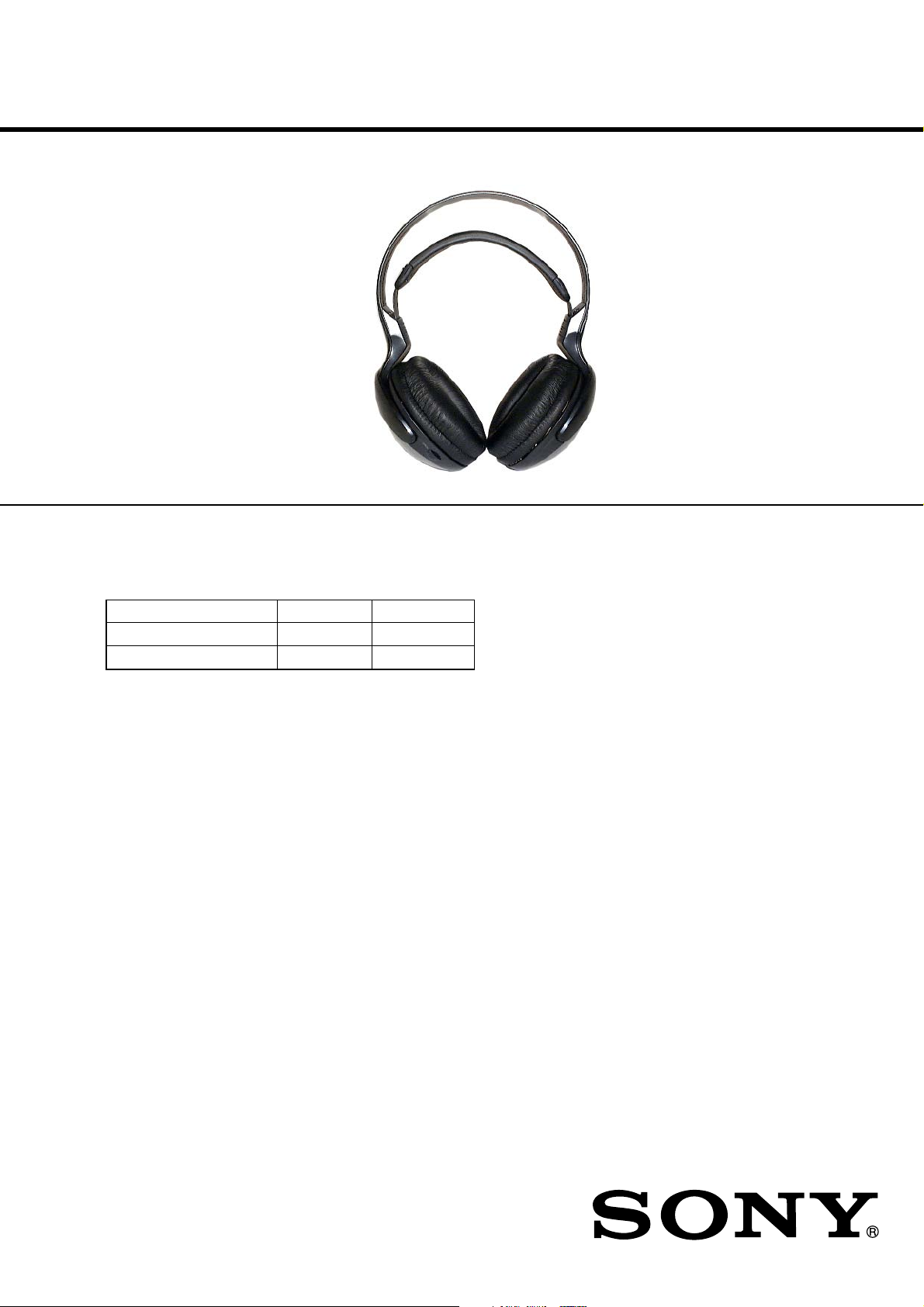
Photo : MDR-RF960R
MDR-RF920R is the component model block one in the MDR-RF920RK.
MDR-RF960R is the component model block one in the MDR-RF960RK.
COMPONENT MODEL NAME FOR MDR-RF920RK/
MDR-RF960RK
MDR-RF920RK MDR-RF960RK
Wireless Stereo Headphones MDR-RF920R MDR-RF960R
Transmitter TMR-RF960R TMR-RF960R
Model
US Model
Canadian Model
SPECIFICATIONS
Headphones
Power source Supplied rechargeable nickelmetal
hydride batteries BPHP550 or commercially
available (size AAA) dry batteries
Mass Approx. 270 g (9.6 oz.) incl.
batteries
Design and specifications are subject to change without notice.
HEADPHONES
9-877-525-02
2006H02-1
© 2006.08
Sony Corporation
Personal Audio Division
Published by Sony Techno Create Corporation
Page 2
MDR-RF920R/RF960R
TABLE OF CONTENTS
Specifications ............................................................................ 1
1. GENERAL ................................................................... 2
2. DISASSEMBLY
2-1. Disassembly Flow ................................................... 3
2-2. Front Plate (R) Assy................................................ 3
2-3. Front Plate (L) Assy ................................................ 4
2-4. SW Board ................................................................ 5
2-5. How to Hang The Tension Spring........................... 5
3. ELECTRICAL ADJUSTMENTS ..........................7
3-1. Free Run Frequency Check and Adjustment........... 7
3-2. Receive Frequency Check and Adjustment ............7
3-3. Carrier Modulation Check ...................................... 7
SECTION 1
GENERAL
3-4. Separation Check ....................................................7
3-5. Free Run Frequency Check and Adjustment........... 8
3-6. Receive Frequency Check and Adjustment ............8
3-7. Carrier Modulation Check ...................................... 8
3-8. Separation Check ....................................................8
4. DIAGRAMS
4-1. Block Diagrams ............................................................... 11
4-2. Schematic Diagram – RX-Base Section (RF920R)– ...... 12
4-3. Schematic Diagram – RX-Base Section (RF960R)– ...... 13
4-4. Printed Wiring Boards– RX-Base Section– .................... 14
4-5. Schematic Diagram – RX-FE Section–........................... 15
4-6. Printed Wiring Boards– RX-FE Section– .......................16
5. EXPLODED VIEWS ................................................. 17
6. ELECTRICAL PARTS LIST ..................................18
This section is extracted
from instruction manual.
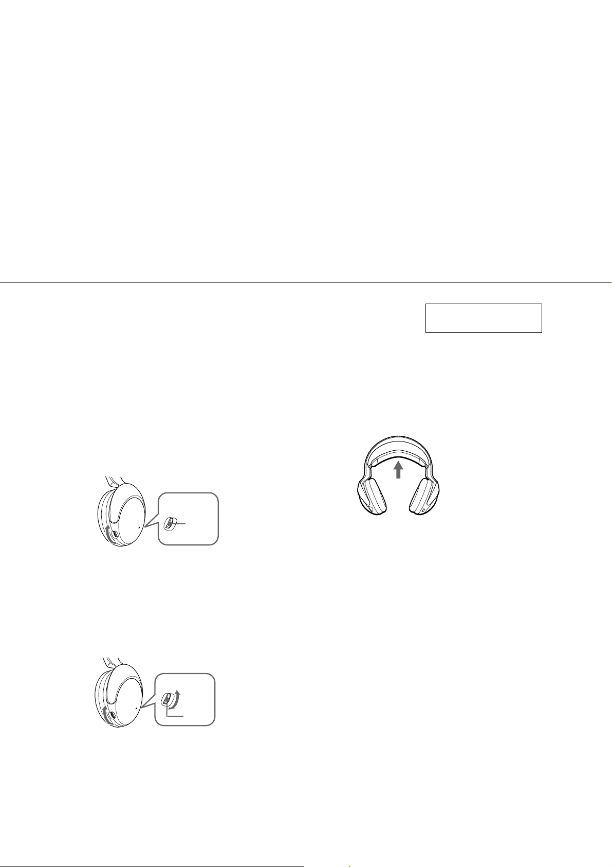
5 Turn up the volume to a moderate
level with the VOL control.
A MDR-RF960R
Press the TUNE button briefly for
automatic tuning of the headphones.
If you do not receive a clear audio
signal, press it again.
TUNE
TUNE
button
VOL control
B MDR-RF920R
Tune the headphones into the frequency
of the transmitter with the TUNE
control until you can hear the audio
signal loud and clear.
The headphones automatically turn
off when the y are taken off
– Auto power on/off function
Do not pull up the self-adjusting band when not
in use, as this will consume the battery power.
Flexible Circuit Board Repairing
• Keep the temperature of the soldering iron around 270°C
during repairing.
• Do not touch the soldering iron on the same conductor of
the circuit board (within 3 times).
• Be careful not to apply force on the conductor when
soldering
TUNE
TUNE
control
VOL control
Follow steps 3 and 5 above until the
receiving performance becomes better.
2
Page 3

• This set can be disassembled in the order shown below.
2-1. DISASSEMBLY FLOW
2-2. Front Plate (R) assy
Set
MDR-RF920R/RF960R
SECTION 2
DISASSEMBLY
(Page 3)
2-3. Front Plate (L) assy
(Page 4)
Note: Follow the disassembly procedure in the numerical order given.
2-2. FRONT PLATE (R) ASSY
8
craw
q;
housing cap (R)
to RX BATTERY
board
RED
2-4. SW baord
(Page 5)
NAT
GRN
6
Remove solder
(4 places)
RX-BASE board
NAT
9
craws
housing (R) sub assy
7
RX-BASE board
4
Remove solder
(2 places)
5
RED
to RX-BASE board
NAT
driver
(R-CH)
to driver (L-CH)
2
three screws
(+B2.6)
3
front plate (R) sub assy
1
ear pad (R)
3
Page 4

MDR-RF920R/RF960R
)
2-3. FRONT PLATE (L) ASSY
7
Remove solder (4 places)
RED
housing (L) sub assy
5
tow screws (DIA. 2)
driver (L-CH)
4
Remove solder
(2 places)
6
GRN
to RX-BASE board
8
RX BATTERY
board
to SW board
NAT
RED
RED
to RX-BASE board
2
three screws
(+B2.6)
3
front plate (L) sub assy
NAT
1
ear pad (L
4
Page 5
)
2-4. SW BOARD
2
hunger (L)
4
hunger (L)
5
6
SW board
MDR-RF920R/RF960R
2-5. HOW TO HANG THE TENSION SPRING
suspender
hanger lid (L)
3
two screws (B2.6
1
two screws (B2.6)
housing (L) sub assy
Note for installation : Insert the end of the
suspender assy under the
S101 on the SW board.
SW board
housing (L) sub assy
tensin spring
suspender
S101
5
Page 6
MDR-RF920R/RF960R
SET THE LEAD WIRES
Set the each lead wires as illustrated below.
a
b
wires
(R-CH)
wires
housing (L)housing (R)
(L-CH)
groove
wire
wires
a
head band
b
6
Page 7
MDR-RF920R
4
+
–+–
IC301 pin6
IC301 pin4
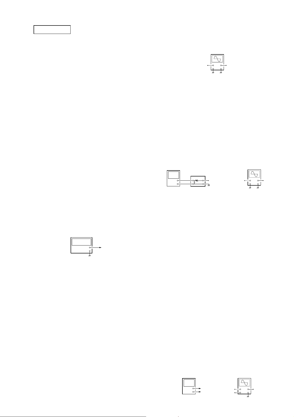
OSCILLOSCPE
CH1 CH2
4
Notes:
1. Use transmitter with check and adjustment alreadycompleted.
2. On adjusting the headphones section, use the transmitter as a
Procedure:
1. Connect an oscillator with attenuator and terminator (600 Ω)
2. Connect an AC adapter to the transmitter DC IN 9V jack
3. Connect a DC 2.4V to the +B power line externally.
4. Connect lead wires to IC301 pin 4, pin 6, pin 7 and GND on
5. Connect a resistor 33k Ω between IC301 pin 4 and pin 7.
6. Connect lead wires to the speakers’ terminals (L+,L-,R+,R-)
3-1. Free Run Frequency Check and Adjustment
1. Set the transmitter AUDIO IN-B connector (J402) to no signal.
Note: In this case, operation time is about 5 or 10 minutes.
Perform confirmation for less than 5 minutes.
2. Check the transmitter power indicator (red) lights.
3. Set the transmitter CHANNEL switch to 1.
4. Set the RV303 (TUNE) to the center position.
5. Connect a frequency counter to IC301 pin 4 and GND on the
6. When the frequency dose not satisfy the specified value, adjust
7. Remove a 33 kΩ resister between IC301 pin 4 and pin 7.
Setting :
3-2. Receive Frequency Check and Adjustment
1. Set the transmitter CHANNEL switch to 2.
2. Set the transmitter NOISE FILTER switch to OFF.
3. Input a signal of 1kHz, 316mVrms to transmitter AUDIO IN-
4. Keep distance between transmitter and headphones to 5 meters
5. Set the headphones volume (RV302) to minimum.
6. Set the RV303 (TUNE) to the center position.
7. Connect an oscilloscope CH1 and CH2 to IC301 pin 6 and
8. Check the waveform of the oscilloscope to CH1 is demodulated
9. If CH1 and CH2 are not satisfied in step 8, adjust the coil
10. Set the transmitter CHANNEL switch to 1.
11. Adjust the RV303 (TUNE) to receive a signal.
12. Check same step 8.
13. Set the transmitter CHANNEL switch to 3.
14. Adjust the RV303 (TUNE) to receive a signal.
15. Check same step 8.
SECTION 3
ELECTRICAL ADJUSTMENTS
jig.
Headphones: MDR-RF920R
Transmitter: TMR-RF960R
to the transmitter AUDIO IN-B connector (J402).
(J403).
the RX-BASE board.
on the RX-BASE board.
RX-BASE board, then confirm the frequency within 76kHz
± 50Hz
the value of the frequency counter to specification by R V301
on the RX-BASE board.
Specified values: 76kHz ± 50Hz.
Frequency counter
+
–
B(L-ch) connector only.
over.
pin 4.
1kHz signal and CH2 is GND.
(L301) on the RX board to satisfied step 8.
Confirm the signal with stereo.
Confirm the signal with stereo.
IC301 pin
MDR-RF920R/RF960R
Setting :
3-3. Carrier Modulation Check
1. Set the transmitter CHANNEL switch to 2.
2. Set the transmitter NOISE FILTER switch to OFF.
3. Input a signal of 1kHz, 316mVrms to transmitter AUDIO INB (L-ch) connector only.
4. Set the headphones volume (RV302) to minimum.
5. Connect an oscilloscope CH1 and CH2 to IC301 pin 6 and
pin 4.
6. Adjust the tuning control (R V303) to receive radio frequency .
7. Check the waveform of the oscilloscope that the CH1 is
demodulated 1kHz signal and CH2 is GND.
8. Connect an AC voltmeter with LPF to IC301 pin 6 and GND.
9. Check the value of the AC voltmeter to 26mVrms ± 2mV.
Setting :
Digital voltmeter
(AC range)
LPF
+
–
2.2K
33000P
IC301
pin6
3-4. Separation Check
1. Set the transmitter CHANNEL switch to 2.
2. Set the transmitter NOISE FILTER switch to OFF.
3. Input a signal of 1kHz, 316mVrms to transmitter AUDIO INB (L-ch) connector only.
4. Connect an oscilloscope CH1 to speakers terminal (L+,L-)
and CH2 to IC301 pin 4 and GND.
5. Adjust the tuning control (R V303) to receive radio frequency .
6. Check the waveform of the oscilloscope that the CH1 is
demodulated 1kHz signal and CH2 is GND.
7. Connect an AC voltmeter with LPF to speakers terminal
(L+,L).
8. Adjust the value of the AC voltmeter to specification by
headphones volume RV302.
Specified values: 155mVrms
9. Connect an AC voltmeter with LPF to speakersterminal
(R+,R-).
10. Measure the value of the AC voltmeter.
11. Check the difference of the L and R to more than 20dB.
12. Input a signal of 1kHz, 316mV rms to transmitter AUDIO INB(R-ch) connector only.
13. Connect an AC voltmeter with LPF to speakers terminal
(R+,R-).
14. Adjust the value of the AC voltmeter to specification by
headphones volume RV302.
Specified values: 155mVrms
15. Connect an AC voltmeter with LPF to speakers terminal
(L+,L-).
16. Measure the value of the AC voltmeter.
17. Check the difference of the L and R to more than 20dB.
Setting :
Digital voltmeter
(AC range)
L+ / R+
+
L– / R–
–
OSCILLOSCPE
IC301 pin6
OSCILLOSCPE
CH1 CH2
+
L+
–+–
L–
CH1 CH2
+
–+–
IC301 pin
IC301 pin4
7
Page 8

MDR-RF920R/RF960R
4
E
MDR-RF960R
Notes:
1. Use transmitter with check and adjustment alreadycompleted.
2. On adjusting the headphones section, use the transmitter as a
jig.
Headphones:MDR-RF960R
Transmitter:TMR-RF960R
Procedure:
1. Connect an oscillator with attenuator and terminator (600 Ω)
to the transmitter AUDIO IN-B connector (J402).
2. Connect an AC adapter to the transmitter DC IN 9V jack
(J403).
3. Short between Q302 corrector and GND on the RX board.
4. Connect a DC 2.4V to the +B power line externally.
5. Connect lead wires to IC301 pin 4, pin 6, pin 7 and GND on
the RX-BASE board.
6. Connect a resistor 33k Ω between IC301 pin 4 and pin 7.
7. Connect lead wires to the speakers’ terminals (L+,L-,R+,R-)
on the RX-BASE board.
3-5. Free Run Frequency Check and Adjustment
1. Set the transmitter AUDIO IN-B connector (J402) to no signal.
Note: In this case, operation time is about 5 or 10 minutes.
Perform confirmation for less than 5 minutes.
2. Check the transmitter power indicator (red) lights.
3. Set the transmitter CHANNEL switch to 1.
4. Connect DC 1.2V across TP (VT) and GND.
5. Connect a frequency counter to IC301 pin 4 and GND on the
RX-BASE board, then confirm the frequency within 76kHz
± 50Hz
6. When the frequency dose not satisfy the specified value, adjust
the value of the frequency counter to specification by R V301
on the RX-BASE board.
Specified values: 76kHz ± 50Hz.
7. Remove a 33 kΩ resister between IC301 pin 4 and pin 7.
Setting :
13. Set the transmitter CHANNEL switch to 1.
14. Push the headphones tuning switch (S301) to receive radio
frequency.
15. Check same step 8.
16. Set the transmitter CHANNEL switch to 3.
17. Push the headphones tuning switch (S301) to receive radio
frequency.
18. Check same step 8.
Setting :
Regulated power supply
(DC 1.2V)
+
TP
–
(VT)
OSCILLOSCPE OSCILLOSCP
IC301
pin6
CH1 CH2
+
–+–
IC301
pin4
TP
(VT)
3-7. Carrier Modulation Check
1. Set the transmitter CHANNEL switch to 2.
2. Set the transmitter NOISE FILTER switch to OFF.
3. Input a signal of 1kHz, 316mVrms to transmitter AUDIO INB (L-ch) connector only.
4. Set the headphones volume (RV302) to minimum.
5. Connect an oscilloscope CH1 and CH2 to IC301 pin 6 and
pin 4.
6. Push the headphone tuning switch (S301) to receive radio
frequency.
7. Check the waveform of the oscilloscope that the CH1 is
demodulated 1kHz signal and CH2 is GND.
8. Connect an AC voltmeter with LPF to IC301 pin 6 and GND.
9. Check the value of the AC voltmeter to 26mVrms ± 2mV.
Setting :
Digital voltmeter
(AC range)
+
–
LPF
2.2K
33000P
IC301
pin6
OSCILLOSCPE
IC301 pin6
CH1 CH2
+
–+–
IC301 pin4
+
–
Regulated power supply
(DC 1.2V)
+
TP
–
(VT)
OSCILLOSCPE
IC301 pin6
CH1 CH2
+
–+–
IC301 pin
3-6. Receive Frequency Check and Adjustment
1. Set the transmitter CHANNEL switch to 2.
2. Set the transmitter NOISE FILTER switch to OFF.
3. Input a signal of 1kHz, 316mVrms to transmitter AUDIO INB(L-ch) connector only.
4. Keep distance between transmitter and headphones to 5 meters
over.
5. Set the headphones volume (RV302) to minimum.
6. Connect DC1.2V across TP (VT) and GND.
7. Connect an oscilloscope CH1 and CH2 to IC301 pin 6 and
pin 4.
8. Check the waveform of the oscilloscope to CH1 is demodulated
1kHz signal and CH2 is GND.
9. If CH1 and CH2 are not satisfied in step 8, adjust the coil (L301)
on the RX board to satisfied step 8.
10. Open between Q302 corrector and GND on the RX board.
11. Connect an oscilloscope to TP (VT).
12. When the transmitter off, check the waveform of the oscilloscope
as follows:
1.8V
8
GND
2-3sec
0.6V
3-8. Separation Check
1. Set the transmitter CHANNEL switch to 2.
2. Set the transmitter NOISE FILTER switch to OFF.
3. Input a signal of 1kHz, 316mVrms to transmitter AUDIO INB (L-ch) connector only.
4. Connect an oscilloscope CH1 to speakers terminal (L+,L-)
and CH2 to IC301 pin 4 and GND.
5. Push the headphones tuning switch (S301) to receive radio
frequency.
6. Check the waveform of the oscilloscope that the CH1 is
demodulated 1kHz signal and CH2 is GND.
7. Connect an AC voltmeter with LPF to speakers terminal
(L+,L-).
8. Adjust the value of the AC voltmeter to specification by
headphones volume RV302.
Specified values: 155mVrms
9. Connect an AC voltmeter with LPF to speakersterminal
(R+,R-).
10. Measure the value of the AC voltmeter.
11. Check the difference of the L and R to more than 20dB.
12. Input a signal of 1kHz, 316mV rms to transmitter AUDIO INB (R-ch) connector only.
13. Connect an AC voltmeter with LPF to speakers terminal
(R+,R-).
14. Adjust the value of the AC voltmeter to specification by
headphones volume RV302.
Specified values: 155mVrms
15. Connect an AC voltmeter with LPF to speakers terminal
(L+,L-).
16. Measure the value of the AC voltmeter.
17. Check the difference of the L and R to more than 20 dB.
Page 9

MDR-RF920R/RF960R
4
Digital voltmeter
(AC range)
L+ / R+
+
L– / R–
–
Asjustment Location :
BOARDRX-BASE (Conductor side)
IC301
IC301
(Connect 33kΩ resistor)
7
4
OSCILLOSCPE
L+
L–
C303
C306
C308
C309
C310
R327
JW307
R328
RV302
N
VOL
CH1 CH2
R334
+
–+–
C369
C361
C362
R333
IC301 pin
R302
C302
C350
C307
RF960RK
R331
CF301
R343
R342
R344
R341
JW310
1
IC302
5
C367
C330
RF960R
D303
R325
R326
R349
R366
R314
C357
C304
R304
C301
C351
R330
JC301
C335
C324
C346
10
6
C331
C328
R316
1
15
JW305
C341
IC303
R351
JW311
C347
R321
IC301
C319
C329
R309
C342
R355
D304
POWER
C326
JW302
R346
R352
R357
R356
C368
R308
R347
R315
30
16
C332
D301
C320
R345
JC308
C325
C327
C305
R305
R310
C333
R340
JC307
L302
C317
TP(VT)
R312
JC310
C314
C315
C336
C313
JC306
+B
R358
JC304
R367
JC305
R362
Q304
JC303
E
IC305
IC304
C358
Q303
C323
1-861-438-
RF920R
R320
Q302
R354
R364
R363
E
JC302
E
R360
L301
R332
R361
R318
RV301
CF302
R323
C318
C311
C312
C316
TUNE
TP(VT)
+B
power line
(DC +2.4V)
Q302
RF920R
RV303
C344
RV303
TUNE(RF920R MODEL)
R+
R–
L+
L–
9
Page 10

MDR-RF920R/RF960R
BOARDRX-BASE (Component side)
RV301: Free Run Frequency Adjustment
RV301
S301
CT1
CT1:
L301
S301: TUNE (RF960R MODEL)
10
Page 11

4-1. BLOCK DIAGRAM
RX-BASE BOARD
ANT301
ANTENNA
RF AMP
I
Q1
FE UNIT
(FRONT END)
CT1
MIX
Q2
OSC
Q3
SECTION 4
DIAGRAMS
O
18
20
FM FE
L302
REG
CF301
CF302
10.7MHz
MDR-RF920R/RF960R
IF AMP/DECODE
IC301
FM IF/
1316
DISCRI
26
AUTO
BLEND
PD1
PD1
1/2
COUNTER
DECODE
AMP
DETUNE
MUTE
TUNING
IND
6 2
5
10
12
R-CH
6 1
DETECT
IC304
Q304
RV302
VOL
IC305
D-FF
POWER AMP
9
IC302
10
1
CK
Q
D
2
CLR
6
3
5
Q
MUTE
Q303
R-CH
SP1
SPEAKER
L-CH
SP2
SPEAKER
R-CH
REG
L301
FM
OSC
L301
RECEIVE
FREQUENCY
21
D301
22
RV303
TUNE
RF920R MODEL
REG
RF960R MODEL
COUNTERCOUNTER
Q4 Q10
7 15
CLOCK OSC/COUNTER
IC303
OSC
Q301
D/A
MUTE
11
SWITCH
Q302
VCO
27
MONO/ST
RV301
FREE RUN
FREQUENCY
SW
STEREO
IND
RF960R MODEL
B+
D304
POWER
(AUTO ON/OFF)
S301
TUNE
B+ SWITCH
Q201,202
S101
S101
1
BATTERY
VOLTAGE
DETECT
IC201
RECHAGEABLE BATTERY
D201
RECHAGEABLE BATTERY
2
NICKEL
(METAL HYDRIDE)
BP-HP550
DRY BATTERY
SIZE "AAA"
(IEC DESIGNATION R03)
2PCS, 2.4V
S201,202
DETECT
S201,202
+
BATTERY
CHARGE
TERMINAL
(TO TMR-RF960R)
–
OR
• R-ch is omitted due to same as L-ch
• Signal path.
F : FM
L : AUDIO
1111
Page 12

MDR-RF920R/RF960R
4-2. SCHEMATIC DIAGRAM – RX-BASE SECTION (RF920R) –
C320
0.1
50V
1
C310
C316
10
16V
L302
0.33µH
0
JW304
1
C331
C317
0.001
C336
56p
C332
56p
JC310
0
C303
16V
C302
0.47
R302
2.2k
C312
3.3
50V
C311
10
CF302
16V
RV301
4.7k
FREE RUN
FREQUENCY
3.3k
R310
4.7
C301
1
IC301
CXA1538N-T4
IF AMP
DECODE
0.022
0.022
3.3k
C305
C304
R304
3.3k
R305
D301
HVU363ATRU
C313
0.01
C314
27p
C315
22p
JC302
C333
3p
C350
1
16V
0.01
22
C307
C306
R312
15k
L301
RECEIVE
FREQUENCY
L301
0
R330
10
16V
50V
1
22
C309
C308
JW310
0
C369
0.01
R331
2.2k
R326
150
C335
0.01
C319
0.01
JC301
JW311
0
0
R308
2.2k
R309
100k
0
JW301
R325
330
C329
0.01
Q304
DTC114TKA-T146
INVERTER
0
JW305
CF301
15
R320
10
JC304
0
R366
150
JW303
JC308
0
7.5k
R347
IC303
SN74HC4060PWR
CLOCK OSC/COUNTER
2SC2412K-T-146-R
D303
RD2.2SB-T1
0
R340
6.8k
30k
R346
Q302
SWITCH
15k
R345
120k
R343
C351
R349
10k
ANT301
ANTENNA
C347
16V
R352
1M
240k
R342
1
C341
0.1
47
62k
R344
R351
100k
470k
R341
JC307
JW302
C346
0.22
R367
47k
0
0
C358
0.001
C342
0.01
R327
15k
R328
15k
JW306
0
R355
47k
R358
22k
JC305
0
JW308
0
R356
22k
R333
2.2k
RV302(1/2)
RV302(2/2)
C361
100p
R334
2.2k
VOL
C367
0.001
IC304
BA10393F-E2
DETECT
R357
22k
2SB1690K
B+ SWITCH
C202
0.001
C330
33
16V
Q201
Q202
2SC2412K-T
B+ SWITCH
R360
22k
S301
R202
1k
IC302
LA4533M-TE-L-E
POWER AMP
C362
100p
R332
R361
22k
C344
0.1
R354
22k
C201
100p
C203
0.01
R203
1M
2SC2412K-T-146-R
R318
47k
1k
SN74AHC2G74HDCTR
R201
10k
Q303
MUTE
C323
R362
10k
R364
22k
IC305
SN74AHC2G
D-FF
R204
100k
XC61CN1902NR
JW307
R314
100k
0.01
C357
10
R315
6.3V
0.1
220
0.1
JC303
C327
C324
0
R363
IC201
0
C325
220
6.3V
C326
220
6.3V
10
R316
0.1
C328
22k
S101
(AUTO ON/OFF)
D201
RB411D
1k
R321
0.01
C368
S202
S201,202
RECHARGEABLE
BATTERY
DETECT
D304
SLC-22VR3F
POWER
BATTERY
CHARGE
TERMINAL
(TO TMR-RF960R)
S201
JW201
0
(IEC DESIGNATION R03)
RECHARGEABLE
(METAL HYDRIDE)
SP1
SPEAKER
L-CH
SP2
SPEAKER
R-CH
DRY BATTERY
SIZE"AAA"
2PCS,3V
OR
BATTERY
BP-HP550
2PCS,2.4V
1212
Page 13

4-3. SCHEMATIC DIAGRAM – RX-BASE SECTION (RF960R) –
C316
10
JC310
0
C311
RV301
4.7k
FREE RUN
FREQUENCY
10
16V
CF302
R310
3.3k
D301
HVU363ATRU
R312
15k
C313
0.01
C314
27p
C312
3.3
C333
50V
RECEIVE
FREQUENCY
C315
15p
5p
C320
0.1
L301
16V
L301
C317
0.001
0
JC302
C318
L302
0.33µH
1
JC306
0
C319
0.01
C336
56p
C332
56p
RV303
10k
JW309
0
R309
100k
R323
6.8k
R308
2.2k
MDR-RF920R/RF960R
15
ANT301
R320
10
JC304
0
ANTENNA
C202
0.001
Q201
2SB1690K
B+ SWITCH
R202
1k
C201
100p
Q202
2SC2412K-T
B+ SWITCH
C203
0.01
R203
1M
R201
10k
R204
100k
IC201
XC61CN1902NR
S101
(AUTO ON/OFF)
D201
RB411D
RECHARGEABLE
S202
S201,202
BATTERY
DETECT
BATTERY
CHARGE
TERMINAL
(TO TMR-RF960R)
S201
JW201
0
DRY BATTERY
SIZE"AAA"
(IEC DESIGNATION R03)
2PCS,3V
OR
RECHARGEABLE
BATTERY
(METAL HYDRIDE)
BP-HP550
2PCS,2.4V
C303
4.7
16V
C302
0.47
R302
2.2k
C304
R304
R305
C305
0.022
3.3k
3.3k
0.022
C301
1
IC301
CXA1538N-T4
IF AMP
DECODE
16V
22
C306
0.01
C307
16V
22
C308
50V
2.2
C309
50V
1
C310
0.01
C369
0.01
C331
R326
150
C335
0.01
R330
10
JW304
0
R325
330
C329
0.01
0
JW301
0
JC301
0
JW305
CF301
R333
2.2k
C361
100p
R334
2.2k
RV302(1/2)
VOL
RV302(2/2)
R327
15k
C350
1
JW308
0
R328
15k
C351
1
C362
100p
C330
33
16V
C367
0.001
IC302
LA4533M-TE-L-E
POWER AMP
C357
0.01
R314
100k
C324
220
6.3V
JW307
0
R315
10
R316
10
C327
0.1
C328
0.1
C325
220
6.3V
C326
220
6.3V
C368
0.01
R321
1k
D304
SLC-22VR3F
POWER
SP1
SPEAKER
L-CH
SP2
SPEAKER
R-CH
1313
Page 14

MDR-RF920R/RF960R
4-4. PRINTED WIRING BOARD – RX-BASE SECTION –
1
2
3 4 5 6 7
8
BOARDSW
A
1-689-785-
BOARDRX-BATTERY
S201
(RECHARGEABLE
BATTERY DETECT)
B
C
DRY BATTERY
SIZE "AAA"
(IEC DESIGNATION R03)
2PCS, 3V
OR
RECHARGEABLE
D
BATTERY
(METAL HYDRIDE)
BP-HP550
2PCS, 2.4V
E
1-861-439-
+-+
BATTERY CHARGE TERMINAL
(TO TMR-RF920R/RF960R)
-
S202
(RECHARGEABLE
BATTERY DETECT)
C205
IC201
Q202
R202
R201
C201
E
JW201
11
(11)
D201
R204
E
R203
C203
Q201
C202
S101
(AUTO ON/OFF)
11
(11)
BOARDRX-BASE
C306
C308
C309
C310
R327
R328
RV302
N
VOL
C303
JW307
R334
C369
C361
C362
R333
C330
R302
C302
C350
C307
RF960R
R331
CF301
R343
R342
R344
R341
JW310
1
IC302
5
C367
RF960R
D303
C304
R330
R325
R326
C335
R349
R366
R314
C357
C324
R304
C301
C351
JC301
C346
10
6
IF
C331
C341
IC303
JW311
C328
R316
SP2
SPEAKER
JW305
R351
C347
POWER
R321
IC301
C319
C329
R309
JW302
C342
R357
R355
D304
C368
C326
R308
R347
R346
R352
R356
R315
A
C332
D301
C320
R345
JC308
C327
(Page 16)
C305
R305
R310
C333
R340
JC307
C325
RX-FE
BOARD
ANT
JC310
C314
L302
C315
C336
C317
TP(VT)
R312
R358
JC304
R367
JC305
R362
Q304
E
C358
C323
1-861-438-
+B
C313
RF920R
JC306
+B
R354
JC303
IC305
IC304
Q303
SP1
SPEAKER
LR
ANT301
R320
Q302
R364
R363
E
JC302
L301
E
R332
R361
R360
R318
RV301
CF302
R323
11
(11)
C318
C311
C312
C316
RV303
TUNE
C344
• Semiconductor
Location
Ref. No. Location
D201 B-4
D301 C-7
D303 D-6
D304 E-7
IC201 C-4
IC301 B-7
IC302 E-6
IC303 D-6
IC304 E-7
IC305 D-7
Q201 D-4
Q202 C-4
Q302 D-7
Q303 E-7
Q304 D-7
RF920R
RF960R
S301
TUNE
F
1414
Page 15

4-5. SCHEMATIC DIAGRAM – RX-FE SECTION –
L8
C1
12nH
0.5p
CN1
L4
1.5T
C3
1p
L5
1.5T
C7
1p
C25
100p
C2
0.001
150
MDR-RF920R/RF960R
R1
390k
R5
150k
CT1
R6
5p
C20
0.001
(RF920R)
12
(RF960R)
13
Q3
2SC5084-OTE85L
OSC
R7
150
C13
C12
11p
3p
X1
433.92
SAW
R10
100k
C29
0.001
CN3
CN2
R8
47k
C14
47p
L6
1.5T
C24
1.5p
C11
0.5p
C22
100p
C19
0.001
C15
100p
C10
0.5p
0.001
JC11
L7
1.5T
C26
1.5p
C23
15p
C40
0
0.33
C28
120p
3SK309
RF AM
L2
µH
Q1
C4
P
1p
R4
470k
C39
0.001
Q2
2SC3120
MIXER
L1
µH
0.33
C5
C8
62p
2p
C9
47p
C30
62p
JC2
C6
0.001
0
• IC Block Diagram
IC302 LA4533M-TE-L-E
POWER
IN-1
PRE-GND
IN-2
REF
1
SWITCH
2
3
4
BIAS
5
POWER SWITCH
AMP 1
AMP 2
MUTE
CIRCUIT
10
MUTE SWITCH
9
OUT-1
8
POWER GND
7
OUT-2
6
VCC
Note on Schematic Diagram:
• All capacitors are in µF unless otherwise noted. pF: µµF 50 WV or
less are not indicated except for electrolytics and tantalums.
• All resistors are in Ω and 1/
• A : B+ Line.
4
W or less unless otherwise specified.
• H : adjustment for repair.
• Power voltage is dc 2.4V and fed with regulated dc power supply
from external power voltage jack.
•Voltages and waveforms are dc with respect to ground under nosignal (detuned) conditions.
•Voltages are taken with a VOM (Input impedance 10 MΩ).
•Waveforms are taken with a oscilloscope.
Voltage variations may be noted due to normal production tolerances.
• Signal path.
F : FM
L : AUDIO
15
Page 16

MDR-RF920R/RF960R
4-6. PRINTED WIRING BOARD – RX-FE SECTION –
A
B
1
BOARDRX-FE
2
(SIDE A)
3
C22
C26
C20
C10
C24
C1
C7
CT1
L2
C12
L1
21
1-688-206-
BOARDRX-FE
(SIDE B)
(21)
C
A
RX-BASE
BOARD
(Page 14)
IF
+B
ANT
• Semiconductor
Location
Ref. No. Location
Q1 C-2
Q2 C-2
Q3 C-3
C3
C2
R5
C9
C8
R7
C11
JC11
C28
R10
L6
C29
L5
C25
JC2
R1
Q1
L4
L8
C39
C15
C4
R4
R6
C30
C5
C23
C40
C6
Q2
L7
1-688-206-
Note on Printed Wiring Boards:
• X : parts extracted from the component side.
®
•
• : Pattern from the side which enables seeing.
Caution:
Pattern face side: Parts on the pattern face side seen from
(Conductor B) the pattern face are indicated.
Parts face side: Parts on the parts face side seen from
(Component A) the parts face are indicated.
: Through hole.
(The other layers' patterns are not indicated.)
X1
C14
C13
Q3
C19
R8
21
(21)
16
Page 17

NOTE:
• -XX, -X mean standardized parts, so they may
have some differences from the original one.
• Items marked “*” are not stocked since they
are seldom required for routine service. Some
delay should be anticipated when ordering these
items.
• The mechanical parts with no reference number
in the exploded views are not supplied.
SECTION 5
EXPLODED VIEWS
• Hardware (# mark) list and accessories are
given in the last of this parts list.
MDR-RF920R/RF960R
Ver. 1.1
10
not
supplied
9
8
10
11
not
supplied
not
supplied
12
not
2
supplied
23
13
not
supplied
9
not
supplied
2
a
14
7
a
SP2
15
2
not
supplied
not
supplied
16
17
18
19
20
not
supplied
2
21
6
22
SP1
4
2
3
Ref. No. Part No. Description Remarks
1 3-246-154-01 PAD (R), EAR (including RX-FE BOARD)(RF920R)
1 3-246-154-13 PAD (R), EAR (including RX-FE BOARD)(RF960R)
2 3-253-143-01 SCREW (B2.6), (+) P TAPPING
* 3 A-4547-109-A RX-BASE BOARD, COMPLETE (RF920R)
* 3 A-4547-111-A RX-BASE BOARD, COMPLETE (RF960R)
4 X-3383-913-1 PLATE (R) SUB ASSY, FRONT (RF960R)
4 X-3383-915-2 PLATE (R) SUB ASSY, FRONT (RF920R)
6 3-251-098-01 HOUSING (R) (RF920R)
6 X-3383-911-1 HOUSING (R) SUB ASSY (RF960R)
7 3-251-102-01 CAP (R), HOUSING (RF920R)
8 3-254-082-11 SCREW
9 4-966-792-01 STOPPER, (LOWER)
10 4-966-791-01 STOPPER (UPPER)
11 3-257-911-01 SPRING, TENSION
12 3-257-555-02 CUSHION (S/W)
13 3-246-137-01 BAND, HEAD
1
Ref. No. Part No. Description Remarks
14 3-246-153-01 PAD (L), EAR (RF920R)
14 3-246-153-13 PAD (L), EAR (RF960R)
15 X-3383-912-1 PLATE (L) SUB ASSY, FRONT (RF960R)
15 X-3383-914-2 PLATE (L) SUB ASSY, FRONT (RF920R)
* 16 A-4547-106-A RX-BATTERY MOUNTED PC BOARD
17 3-246-151-03 TERMINAL (-), BATTERY
18 3-246-150-02 TERMINAL (+), BATTERY
19 3-246-152-02 TERMINAL, CHARGE
20 3-246-148-01 BUTTON
21 3-246-142-01 HOUSING (L)
22 3-251-101-11 LID, BATTERY (RF920R)
22 3-251-108-11 LID, BATTERY (RF960R)
23 A-1133-212-A BAND ASSY, HEAD (RF920R)
23 A-1133-225-A BAND ASSY, HEAD (RF960R)
SP1 1-542-400-11 DRIVER (030F032) (L-CH)
SP2 1-542-400-11 DRIVER (030F032) (R-CH)
17
Page 18

MDR-RF920R/RF960R
RX-BASE RX-FE
SECTION 6
ELECTRICAL PARTS LIST
NOTE:
• Due to standardization, replacements in the
parts list may be different from the parts
specified in the diagrams or the components
used on the set.
• -XX, -X mean standardized parts, so they
may have some difference from the original
one.
• Items marked “*” are not stocked since they
are seldom required for routine service.
Some delay should be anticipated when
ordering these items.
• CAPACITORS:
uF: µF
Ref. No. Part No. Description Remarks Ref. No. Part No. Description Remarks
* A-4547-109-A RX-BASE BOARD, COMPLETE
(including RX-FE BOARD)(RF920R)
* A-4547-111-A RX-BASE BOARD, COMPLETE
(including RX-FE BOARD)(RF960R)
• RESISTORS
All resistors are in ohms.
METAL: metal-film resistor
METAL OXIDE: Metal Oxide-film resistor
F: nonflammable
• COILS
uH: µH
•SEMICONDUCTORS
In each case, u: µ, for example:
uA...: µA... , uPA... , µPA... ,
uPB... , µPB... , uPC... , µPC... ,
uPD..., µPD...
C310 1-123-611-61 ELECT 1uF 20% 50V
C311 1-124-233-11 ELECT 10uF 20% 16V
C312 1-126-162-11 ELECT 3.3uF 20% 50V
When indicating parts by reference
number, please include the board.
(RF960R)
*********************
C313 1-162-970-11 CERAMIC CHIP 0.01uF 10% 25V
< CAPACITOR >
C1 1-167-494-11 CERAMIC CHIP 0.5PF 0.1PF 50V
C2 1-162-964-11 CERAMIC CHIP 0.001uF 10% 50V
C3 1-162-905-11 CERAMIC CHIP 1PF 0.25PF 50V
C4 1-162-905-11 CERAMIC CHIP 1PF 0.25PF 50V
C5 1-164-381-91 CERAMIC CHIP 62PF 5% 50V
C6 1-162-964-11 CERAMIC CHIP 0.001uF 10% 50V
C7 1-162-905-11 CERAMIC CHIP 1PF 0.25PF 50V
C8 1-162-907-11 CERAMIC CHIP 2PF 0.25PF 50V
C9 1-162-923-11 CERAMIC CHIP 47PF 5% 50V
C10 1-107-494-11 CERAMIC CHIP 0.5PF 0.1PF 50V
C11 1-107-494-11 CERAMIC CHIP 0.5PF 0.1PF 50V
C12 1-164-376-11 CERAMIC CHIP 11PF 5% 50V
C13 1-162-908-11 CERAMIC CHIP 3PF 0.25PF 50V
C14 1-162-923-11 CERAMIC CHIP 47PF 5% 50V
C15 1-162-927-11 CERAMIC CHIP 100PF 5% 50V
C19 1-162-964-11 CERAMIC CHIP 0.001uF 10% 50V
C20 1-162-964-11 CERAMIC CHIP 0.001uF 10% 50V
C22 1-162-927-11 CERAMIC CHIP 100PF 5% 50V
C23 1-162-917-11 CERAMIC CHIP 15PF 5% 50V
C24 1-162-906-11 CERAMIC CHIP 1.5PF 0.25PF 50V
C25 1-162-927-11 CERAMIC CHIP 100PF 5% 50V
C26 1-162-906-11 CERAMIC CHIP 1.5PF 0.25PF 50V
C28 1-162-928-11 CERAMIC CHIP 120PF 5% 50V
C29 1-162-964-11 CERAMIC CHIP 0.001uF 10% 50V
C30 1-164-381-91 CERAMIC CHIP 62PF 5% 50V
C39 1-162-964-11 CERAMIC CHIP 0.001uF 10% 50V
C40 1-162-964-11 CERAMIC CHIP 0.001uF 10% 50V
C301 1-165-908-11 CERAMIC CHIP 1uF 10% 10V
C302 1-125-891-11 CERAMIC CHIP 0.47uF 10% 10V
C303 1-124-231-61 ELECT 4.7uF 20% 16V
C314 1-164-239-91 CERAMIC CHIP 27PF 5% 50V
C315 1-162-917-11 CERAMIC CHIP 15PF 5% 50V
(RF920R)
C315 1-162-919-11 CERAMIC CHIP 22PF 5% 50V
(RF960R)
C316 1-124-233-11 ELECT 10uF 20% 16V
C317 1-162-964-11 CERAMIC CHIP 0.001uF 10% 50V
C318 1-165-908-11 CERAMIC CHIP 1uF 10% 10V
(RF920R)
C319 1-162-970-11 CERAMIC CHIP 0.01uF 10% 25V
C320 1-107-826-11 CERAMIC CHIP 0.1uF 10% 16V
C323 1-107-826-11 CERAMIC CHIP 0.1uF 10% 16V
(RF960R)
C324 1-124-635-00 ELECT 220uF 20% 6.3V
C325 1-124-635-00 ELECT 220uF 20% 6.3V
C326 1-124-635-00 ELECT 220uF 20% 6.3V
C327 1-107-826-11 CERAMIC CHIP 0.1uF 10% 16V
C328 1-107-826-11 CERAMIC CHIP 0.1uF 10% 16V
C329 1-162-970-11 CERAMIC CHIP 0.01uF 10% 25V
C330 1-124-242-00 ELECT 33uF 20% 25V
C331 1-162-970-11 CERAMIC CHIP 0.01uF 10% 25V
(RF920R)
C331 1-165-908-11 CERAMIC CHIP 1uF 10% 10V
(RF960R)
C332 1-162-924-11 CERAMIC CHIP 56PF 5% 50V
C333 1-162-910-11 CERAMIC CHIP 5PF 0.25PF 50V
(RF920R)
C333 1-162-908-11 CERAMIC CHIP 3PF 0.25PF 50V
(RF960R)
C335 1-162-970-11 CERAMIC CHIP 0.01uF 10% 25V
C336 1-162-924-11 CERAMIC CHIP 56PF 5% 50V
C341 1-107-826-11 CERAMIC CHIP 0.1uF 10% 16V
(RF960R)
C304 1-164-227-11 CERAMIC CHIP 0.022uF 10% 25V
C305 1-164-227-11 CERAMIC CHIP 0.022uF 10% 25V
C306 1-124-234-00 ELECT 22uF 20% 16V
C307 1-162-970-11 CERAMIC CHIP 0.01uF 10% 25V
C308 1-124-234-00 ELECT 22uF 20% 16V
C309 1-124-257-00 ELECT 2.2uF 20% 50V
C309 1-123-611-61 ELECT 1uF 20% 50V
18
(RF920R)
C342 1-162-970-11 CERAMIC CHIP 0.01uF 10% 25V
(RF960R)
C344 1-107-826-11 CERAMIC CHIP 0.1uF 10% 16V
(RF960R)
C346 1-127-715-91 CERAMIC CHIP 0.22uF 10% 16V
(RF960R)
C347 1-124-589-11 ELECT 47uF 20% 16V
(RF960R)
C350 1-165-908-11 CERAMIC CHIP 1uF 10% 10V
Page 19

MDR-RF920R/RF960R
RX-BASE RX-FE
Ref. No. Part No. Description Remarks Ref. No. Part No. Description Remarks
C351 1-165-908-11 CERAMIC CHIP 1uF 10% 10V
C357 1-162-970-11 CERAMIC CHIP 0.01uF 10% 25V
C358 1-162-964-11 CERAMIC CHIP 0.001uF 10% 50V
(RF960R)
C361 1-162-927-11 CERAMIC CHIP 100PF 5% 50V
C362 1-162-927-11 CERAMIC CHIP 100PF 5% 50V
C367 1-162-964-11 CERAMIC CHIP 0.001uF 10% 50V
C368 1-162-970-11 CERAMIC CHIP 0.01uF 10% 25V
C369 1-162-970-11 CERAMIC CHIP 0.01uF 10% 25V
< FILTER >
CF301 1-760-235-81 FILTER, CERAMIC
CF302 1-579-392-81 FILTER, CERAMIC(DISCRIMINATOR)
< TRIMMER >
Q1 8-729-040-64 TRANSISTOR 3SK309XV-TL
Q2 8-729-209-45 TRANSISTOR 2SC3120-TE85R
Q3 8-729-043-92 TRANSISTOR 2SC5084-0(TE85L)
Q302 8-729-901-81 TRANSISTOR 2SC2412K-T-146-R (RF960R)
Q303 8-729-901-81 TRANSISTOR 2SC2412K-T-146-R (RF960R)
Q304 8-729-027-44 TRANSISTOR DTC114TKA-T146 (RF960R)
R1 1-216-852-11 METAL CHIP 390K 5% 1/10W
R4 1-216-853-11 METAL CHIP 470K 5% 1/10W
R5 1-216-847-11 METAL CHIP 150K 5% 1/10W
R6 1-216-811-11 METAL CHIP 150 5% 1/10W
R7 1-216-811-11 METAL CHIP 150 5% 1/10W
< TRANSISTOR >
< RESISTOR >
CT1 1-141-325-11 CAP, CHIP TYPE TRIMMER 5PF
< DIODE >
D301 8-719-083-90 DIODE HVU363ATRU
D303 8-719-036-66 DIODE RD2.2SB-T1
D304 8-719-941-07 DIODE SLC-22VR3 (POWER)
< IC >
IC301 8-752-072-12 IC CXA1538N-T4
IC302 6-704-731-01 IC LA4533M-TE-L-E
IC303 6-705-851-01 IC SN74HC4060PWR (RF960R)
IC304 8-759-510-73 IC BA10393F-E2 (RF960R)
IC305 6-702-827-01 IC SN74AHC2G74HDCTR (RF960R)
< JUMPER RESISTOR >
JC2 1-216-864-11 METAL CHIP 0 5% 1/10W
JC11 1-216-864-11 METAL CHIP 0 5% 1/10W
JC301 1-216-864-11 METAL CHIP 0 5% 1/10W
JC302 1-216-864-11 METAL CHIP 0 5% 1/10W
JC303 1-216-864-11 METAL CHIP 0 5% 1/10W
(RF960R)
JC304 1-216-864-11 METAL CHIP 0 5% 1/10W
JC305 1-216-864-11 METAL CHIP 0 5% 1/10W
(RF960R)
JC306 1-216-864-11 METAL CHIP 0 5% 1/10W
(RF920R)
JC307 1-216-864-11 METAL CHIP 0 5% 1/10W
(RF960R)
JC308 1-216-864-11 METAL CHIP 0 5% 1/10W
(RF960R)
JC310 1-216-864-11 METAL CHIP 0 5% 1/10W
< COIL >
L1 1-412-933-11 INDUCTOR 0.33uH
L2 1-412-933-11 INDUCTOR 0.33uH
L4 1-416-821-12 COIL , AIR-CORE
L5 1-416-821-12 COIL , AIR-CORE
L6 1-416-821-12 COIL , AIR-CORE
R8 1-216-841-11 METAL CHIP 47K 5% 1/10W
R10 1-216-845-11 METAL CHIP 100K 5% 1/10W
R302 1-216-825-11 METAL CHIP 2.2K 5% 1/10W
R304 1-216-827-11 METAL CHIP 3.3K 5% 1/10W
R305 1-216-827-11 METAL CHIP 3.3K 5% 1/10W
R308 1-216-825-11 METAL CHIP 2.2K 5% 1/10W
R309 1-216-845-11 METAL CHIP 100K 5% 1/10W
R310 1-216-827-11 METAL CHIP 3.3K 5% 1/10W
R312 1-216-835-11 METAL CHIP 15K 5% 1/10W
R314 1-216-845-11 METAL CHIP 100K 5% 1/10W
R315 1-216-797-11 METAL CHIP 10 5% 1/10W
R316 1-216-797-11 METAL CHIP 10 5% 1/10W
R318 1-216-841-11 METAL CHIP 47K 5% 1/10W
(RF960R)
R320 1-216-797-11 METAL CHIP 10 5% 1/10W
R321 1-216-821-11 METAL CHIP 1K 5% 1/10W
R323 1-218-867-11 METAL CHIP 6.8K 5% 1/10W
(RF920R)
R325 1-216-815-11 METAL CHIP 330 5% 1/10W
R326 1-216-811-11 METAL CHIP 150 5% 1/10W
R327 1-216-835-11 METAL CHIP 15K 5% 1/10W
R328 1-216-835-11 METAL CHIP 15K 5% 1/10W
R330 1-216-797-11 METAL CHIP 10 5% 1/10W
R331 1-216-825-11 METAL CHIP 2.2K 5% 1/10W
(RF960R)
R332 1-216-821-11 METAL CHIP 1K 5% 1/10W
(RF960R)
R333 1-216-825-11 METAL CHIP 2.2K 5% 1/10W
R334 1-216-825-11 METAL CHIP 2.2K 5% 1/10W
R340 1-218-867-11 METAL CHIP 6.8K 5% 1/10W
(RF960R)
R341 1-216-853-11 METAL CHIP 470K 5% 1/10W
(RF960R)
R342 1-218-749-11 METAL CHIP 240K 5% 1/10W
(RF960R)
R343 1-216-846-11 METAL CHIP 120K 5% 1/10W
(RF960R)
R344 1-218-890-11 METAL CHIP 62K 5% 1/10W
(RF960R)
L7 1-416-821-12 COIL , AIR-CORE
L8 1-414-665-11 INDUCTOR 12nH
L301 1-428-911-11 COIL, AIR-CORE
L302 1-412-933-11 INDUCTOR 0.33uH
R345 1-216-835-11 METAL CHIP 15K 5% 1/10W
(RF960R)
R346 1-218-727-11 METAL CHIP 30K 5% 1/10W
(RF960R)
R347 1-218-344-11 METAL CHIP 7.5K 5% 1/10W
(RF960R)
19
Page 20

MDR-RF920R/RF960R
RX-FE RX-BATTERY SWRX-BASE
Ref. No. Part No. Description Remarks Ref. No. Part No. Description Remarks
R349 1-216-833-11 METAL CHIP 10K 5% 1/10W
(RF960R)
R351 1-216-845-11 METAL CHIP 100K 5% 1/10W
(RF960R)
R352 1-216-857-11 METAL CHIP 1M 5% 1/10W
(RF960R)
R354 1-216-837-11 METAL CHIP 22K 5% 1/10W
(RF960R)
R355 1-216-841-11 METAL CHIP 47K 5% 1/10W
(RF960R)
R356 1-216-837-11 METAL CHIP 22K 5% 1/10W
(RF960R)
R357 1-216-837-11 METAL CHIP 22K 5% 1/10W
(RF960R)
R358 1-216-837-11 METAL CHIP 22K 5% 1/10W
(RF960R)
R360 1-216-837-11 METAL CHIP 22K 5% 1/10W
(RF960R)
R361 1-216-837-11 METAL CHIP 22K 5% 1/10W
(RF960R)
R362 1-216-833-11 METAL CHIP 10K 5% 1/10W
(RF960R)
R363 1-216-837-11 METAL CHIP 22K 5% 1/10W
(RF960R)
R364 1-216-837-11 METAL CHIP 22K 5% 1/10W
(RF960R)
R366 1-216-811-11 METAL CHIP 150 5% 1/10W
(RF960R)
R367 1-216-841-11 METAL CHIP 47K 5% 1/10W
(RF960R)
Q202 8-729-901-81 TRANSISTOR 2SC2412K-T-146-R
< RESISTOR >
R201 1-216-833-11 METAL CHIP 10K 5% 1/10W
R202 1-216-821-11 METAL CHIP 1K 5% 1/10W
R203 1-216-857-11 METAL CHIP 1M 5% 1/10W
R204 1-216-845-11 METAL CHIP 100K 5% 1/10W
< SWITCH >
S201 1-786-130-11 SWITCH, PUSH (1 KEY)
(RECHERGABLE BATTERY DET)
S202 1-762-917-11 SWITCH, DETECTION (SMALL TYPE)
(RECHERGABLE BATTERY DET)
******************************************************
SW BOARD
*********
< SWITCH >
S101 1-762-003-11 SWITCH, PUSH (AUTO ON/OFF)
******************************************************
MISCELLANEOUS
*************
SP1 1-542-400-11 DRIVER (030F032) (L-CH)
SP2 1-542-400-11 DRIVER (030F032) (R-CH)
******************************************************
< VARIABLE RESISTOR >
RV301 1-241-763-11 RES, ADJ, CARBON 4.7K
(FREE RUN FREQUENCY)
< SWITCH >
S301 1-786-596-11 SWITCH, TACTILE (TUNE) (RF960R)
< RESONATOR >
X1 1-813-239-11 RESONATOR, SAW
******************************************************
* A-4547-106-A RX-BATTERY BOARD, COMPLETE
************************
< CAPACITOR >
C201 1-162-927-11 CERAMIC CHIP 100PF 5% 50V
C202 1-162-964-11 CERAMIC CHIP 0.001uF 10% 50V
C203 1-162-970-11 CERAMIC CHIP 0.01uF 10% 25V
< DIODE >
D201 8-719-975-40 DIODE RB411D
< IC >
IC201 6-702-083-01 IC XC61CN1902NR
< TRANSISTOR >
Q201 6-550-363-01 TRANSISTOR 2SB1690KT146
20
Page 21

MEMO
MDR-RF920R/RF960R
21
Page 22

MDR-RF920R/RF960R
REVISION HISTORY
Clicking the version allows you to jump to the revised page.
Also, clicking the version at the upper right on the revised page allows you to jump to the next revised
page.
Ver. Date Description of Revision
1.0 2004.02 New
1.1 2006.08 Addition of Ref. No. 23 BAND ASSY, HEAD. (SPM-06096)
Addition of US model.
 Loading...