

Page 1

MDR-RF915R/RF945R
SERVICE MANUAL
Ver 1.0 2001. 05
Photo : MDR-RF945R
MDR-RF915R is the component model block one in the MDR-RF915RK.
MDR-RF945R is the component model block one in the MDR-RF945RK.
COMPONENT MODEL NAME FOR MDR-RF915RK/
MDR-RF945RK
MDR-RF915RK MDR-RF945RK
Wireless Stereo Headphones MDR-RF915R MDR-RF945
Transmitter TMR-RF915R TMR-RF945
US Model
Canadian Model
SPECIFICATIONS
Headphones
Power source DC 2.4 V: Built-in rechargeable
battery
Mass Approx. 240 g (8.5 oz.) incl.
built-in rechargeable battery
Built-in Ni-Cd rechargeable battery
Model name NC-AA
Voltage 1.2 V
Capacity 700 mAh
Design and specifications are subject to change without
notice.
HEADPHONES
9-873-137-11
2001E0200-1
© 2001.5
Sony Corporation
Personal Audio Company
Shinagawa Tec Service Manual Production Group
Page 2
MDR-RF915R/RF945R
f
TABLE OF CONTENTS
Specifications ............................................................................ 1
1. GENERAL ....................................................................... 2
2. DISASSEMBLY
2-1. RX-BASE Board ...................................................... 3
3-5. Free Run Frequency
Check and Adjustment (MRD-RF945R).........6
3-6. Receive Frequency
Check and Adjustment (MRD-RF945R)......... 6
3-7. Carrier Modulation Check (MRD-RF945R) ............... 6
3-8. Separation Check (MRD-RF945R) ............................. 6
3. ELECTRICAL ADJUSTMENTS..............................4
3-1. Free Run Frequency
Check and Adjustment (MRD-RF915R) ....... 5
3-2. Receive Frequency
Check and Adjustment (MRD-RF915R) ....... 5
3-3. Carrier Modulation Check (MRD-RF915R) ............. 5
3-4. Separation Check (MRD-RF915R) ........................... 5
SECTION 1
GENERAL
A
5
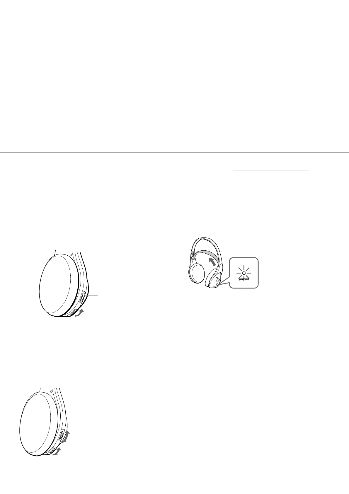
- Turn up the volume to a moderate
level with the VOL control.
Press the TUNING button briefly for
automatic tuning of the headphones.
If you do not receive a clear audio
signal, press it again.
A
MDR-RF945RK
4. DIAGRAMS
4-1. Block Diagrams ........................................................... 8
4-2. Schematic Diagram ..................................................... 9
4-3. Printed Wiring Board................................................. 10
5. EXPLODED VIEWS........................................................11
6. ELECTRICAL PARTS LIST........................................12
This section is extracted from
instruction manual.
Auto power on/off function
When you remove the headphones from your
head, the power turns off automatically. Do not
allow the self adjusting band to be pulled up,
otherwise the headphones will be switched on.
TUNING
button
VOL control
B
5
- Turn up the volume to a moderate
level with the VOL control, then tune
the headphones in to the frequency o
the transmitter with the TUNING
control until you can hear the audio
signal loud and clear.
MDR-RF915RK
B
TUNING
control
VOL control
Try the above steps 3 and 5 until the
receiving performance becomes better.
2
The power turns on.
SAFETY CHECK-OUT
After correcting the original service problem, perform the
following safety checks before releasing the set to the
customer.
1. Check the area of your repair for unsoldered or poorly-sol
deredconnections. Check the entire board surface for solder
splashes and bridges.
2. Check the interboard wiring to ensure that no wires are
“pinched” or contact high-wattage resistors.
3. Look for unauthorized replacement parts, particularlyt ransis
tors, that were installed during a previous repair.
Point them out to the customer and recommend their
replacement.
4. Look for parts which, through functioning, show obvious
signs of deterioration. Point them out to the customer
and recommend their replacement.
5. Check the B+ voltage to see it is at the values specified.
6. Flexible Circuit Board Repairing
• Keep the temperature of the soldering iron around 270°C
during repairing.
• Do not touch the soldering iron on the same conductor of
the circuit board (within 3 times).
• Be careful not to apply force on the conductor when
soldering
Page 3
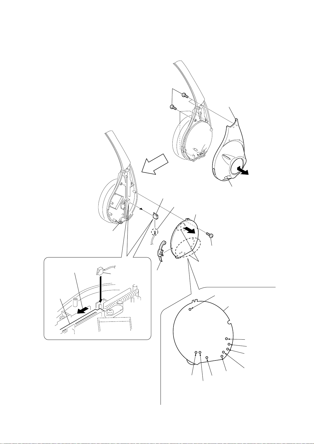
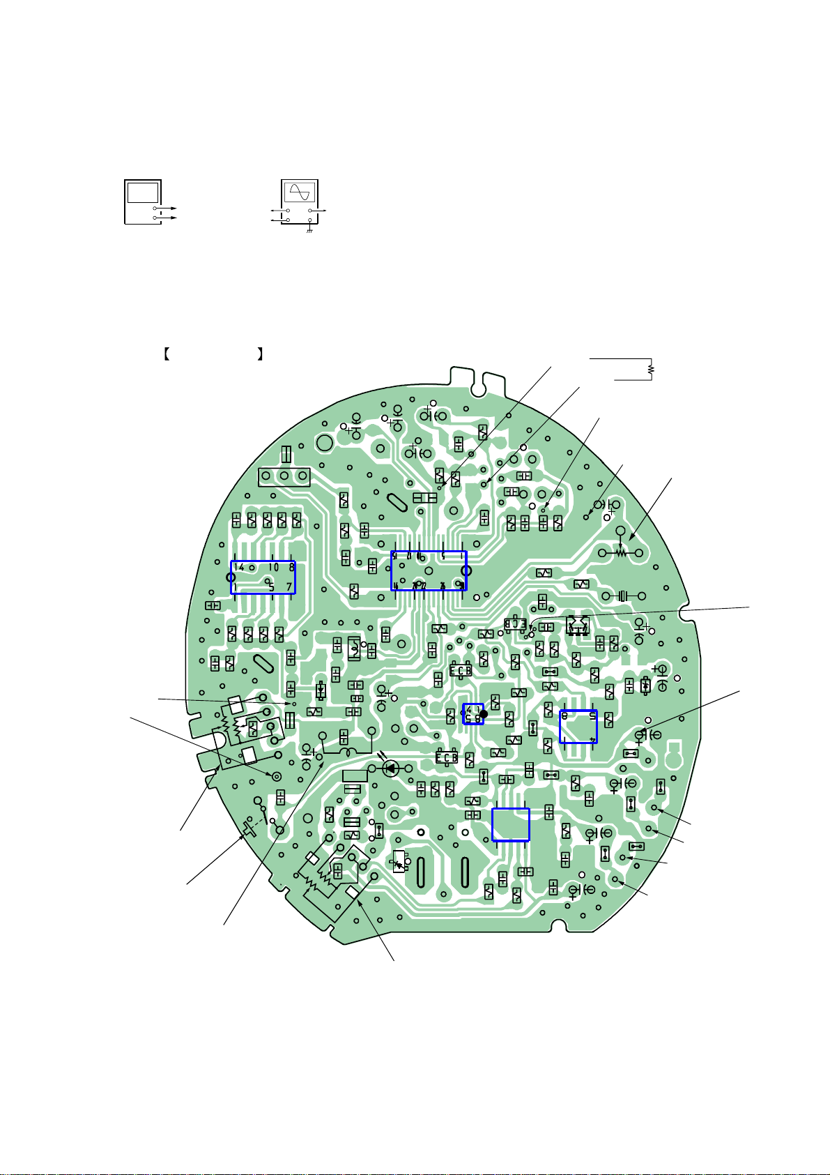
• This set can be disassembled in the order shown below.
2-1. RX-BASE BOARD
1
SECTION 2
DISASSEMBLY
Five screws (P 2
× 6)
MDR-RF915R/RF945R
Cover (R), hanger
Claw
Precaution for installtion
1
Slide the suspender in the
direction of the arrow.
Suspender
2
Set the psuh
switch (1 key).
8
6
(RF945R)
q;
Switch, push (1 key)
9
Remove the two solderings.
Button, tuning
7
RX-BASE board
5
3
Remove the
nine solderings.
2
Claw
4
Screw (P 2
× 8)
Precaution for installtion
No.205
RX-BASE board
No.204
No.201
No.201 (green)
No.202
No.203
No.203 (black)
Solder the each lead wires directly to the position as shown
while being cautions of colors.
No.204
No.202 (red)
3
Page 4
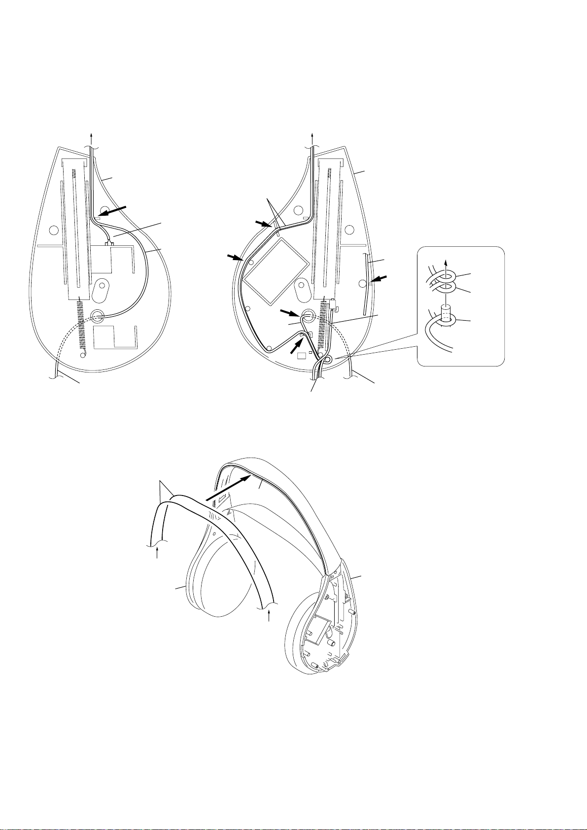
MDR-RF915R/RF945R
Set the lead wires
Set the each lead wires as illustrated below.
B
Cover (L), hanger
Groove
To the driver (030F032).
No.203
No.201
Groove
No.201, No.203
Groove
Groove
No.202
Groove
To the RX-BASE board
A
Cover (R), hanger
No.205
Groove
No.204
To the driver (030F032).
No.201
No.203
No.202
No.201, No.203
B
Cover (L), hanger
Groove
Cover (R), hanger
A
4
Page 5

SECTION 3
4
+
–+–
IC301 pin6
IC301 pin4
OSCILLOSCPE
CH1 CH2
4
MRD-RF915R
Notes:
1. Use transmitter with check and adjustment alreadycompleted.
2. On adjusting the headphones section, use the transmitter as a
jig.
Headphones:MDR-RF915R
Transmitter:TMR-RF915R
ELECTRICAL ADJUSTMENTS
MDR-RF915R/RF945R
Setting :
Procedure:
1. Connect an oscillator with attenuator and terminator (600 Ω)
2. Connect an AC adapter to the transmitter DC IN 9V jack (J404).
3. Connect a DC 2.4V to the +B power line externally.
4. Connect lead wires to IC301 pin 4, pin 6, pin 7 and GND on
5. Connect a resistor 33k Ω between IC301 pin 4 and pin 7.
6. Connect lead wires to the speakers’ terminals (L+,L-,R+,R-)
3-1. Free Run Frequency Check and Adjustment
1. Set the transmitter AUDIO IN-A connector (J402) to no signal.
Note: In this case, operation time is about 5 or 10 minutes.
2. Check the transmitter power indicator (red) lights.
3. Set the transmitter CHANNEL switch to 1.
4. Set the RV303 (TUNE) to the center position.
5. Connect a frequency counter to IC301 pin 4 and GND on the
6. When the frequency dose not satisfy the specified value, adjust
7. Remove a 33 Ω resister between IC301 pin 4 and pin 7.
Setting :
3-2. Receive Frequency Check and Adjustment
1. Set the transmitter CHANNEL switch to 2.
2. Set the transmitter NOISE FILTER switch to OFF.
3. Input a signal of 1kHz, 316mVrms to transmitter AUDIO IN-
4. Keep distance between transmitter and headphones to 5 meters
5. Set the headphones volume (RV302) to minimum.
6. Set the RV303 (TUNE) to the center position.
7. Connect an oscilloscope CH1 and CH2 to IC301 pin 6 and
8. Check the waveform of the oscilloscope to CH1 is demodulated
9. If CH1 and CH2 are not satisfied in step 8, adjust the coil (L301)
10. Set the transmitter CHANNEL switch to 1.
11. Adjust the RV303 (TUNE) to receive a signal.
12. Check same step 8.
13. Set the transmitter CHANNEL switch to 3.
14. Adjust the RV303 (TUNE) to receive a signal.
15. Check same step 8.
to the transmitter AUDIO IN-A connector (J402).
the RX-BASE board.
on the RX-BASE board.
Perform confirmation for less than 5 minutes.
RX-BASE board, then confirm the frequency within 76kHz
± 50Hz
the value of the frequency counter to specification by RV301
on the RX-BASE board.
Specified values: 76kHz ± 50Hz.
Frequency counter
+
–
IC301 pin
A(L-ch) connector only.
over.
pin 4.
1kHz signal and CH2 is GND.
on the RX board to satisfied step 8.
Confirm the signal with stereo.
Confirm the signal with stereo.
3-3. Carrier Modulation Check
1. Set the transmitter CHANNEL switch to 2.
2. Set the transmitter NOISE FILTER switch to OFF.
3. Input a signal of 1kHz, 316mVrms to transmitter AUDIO IN-A
(L-ch) connector only.
4. Set the headphones volume (RV302) to minimum.
5. Connect an oscilloscope CH1 and CH2 to IC301 pin 6 and
pin 4.
6. Adjust the tuning control (RV303) to receive radio frequency.
7. Check the waveform of the oscilloscope that the CH1 is
demodulated 1kHz signal and CH2 is GND.
8. Connect an AC voltmeter with LPF to IC301 pin 6 and GND.
9. Check the value of the AC voltmeter to 26mVrms ± 2mV
Setting :
Digital voltmeter
(AC range)
+
–
LPF
2.2K
33000P
IC301
pin6
OSCILLOSCPE
IC301 pin6
CH1 CH2
+
–+–
IC301 pin4
3-4. Separation Check
1. Set the transmitter CHANNEL switch to 2.
2. Set the transmitter NOISE FILTER switch to OFF.
3. Input a signal of 1kHz, 316mVrms to transmitter AUDIO IN-A
(L-ch) connector only.
4. Connect an oscilloscope CH1 to speakers terminal (L+,L-) and
CH2 to IC301 pin 4 and GND.
5. Adjust the tuning control (RV303) to receive radio frequency.
6. Check the waveform of the oscilloscope that the CH1 is
demodulated 1kHz signal and CH2 is GND.
7. Connect an AC voltmeter with LPF to speakers terminal (L+,L).
8. Adjust the value of the AC voltmeter to specification by
headphones volume RV302.
Specified values: 155mVrms
9. Connect an AC voltmeter with LPF to speakersterminal
(R+,R-).
10. Measure the value of the AC voltmeter.
11. Check the difference of the L and R to more than 20dB.
12. Input a signal of 1kHz, 316mVrms to transmitter AUDIO IN-A
(R-ch) connector only.
13. Connect an AC voltmeter with LPF to speakers terminal
(R+,R-).
14. Adjust the value of the AC voltmeter to specification by
headphones volume RV302.
Specified values: 155mVrms
15. Connect an AC voltmeter with LPF to speakers terminal
(L+,L-).
16. Measure the value of the AC voltmeter.
17. Check the difference of the L and R to more than 20dB.
Setting :
Digital voltmeter
(AC range)
+
–
L+ / R+
L– / R–
OSCILLOSCPE
CH1 CH2
+
L+
–+–
L–
IC301 pin
5
Page 6
MDR-RF915R/RF945R
4
4
MRD-RF945R
Notes:
1. Use transmitter with check and adjustment alreadycompleted.
2. On adjusting the headphones section, use the transmitter as a
jig.
Headphones:MDR-RF945R
Transmitter:TMR-RF945R
Procedure:
1. Connect an oscillator with attenuator and terminator (600 Ω)
to the transmitter AUDIO IN-A connector (J402).
2. Connect an AC adapter to the transmitter DC IN 9V jack (J404).
3. Short between Q303 corrector and GND on the RX board.
4. Connect a DC 2.4V to the +B power line externally.
5. Connect lead wires to IC301 pin 4, pin 6, pin 7 and GND on
the RX-BASE board.
6. Connect a resistor 33k Ω between IC301 pin 4 and pin 7.
7. Connect lead wires to the speakers’ terminals (L+,L-,R+,R-)
on the RX-BASE board.
3-5. Free Run Frequency Check and Adjustment
1. Set the transmitter AUDIO IN-A connector (J402) to no signal.
Note: In this case, operation time is about 5 or 10 minutes.
Perform confirmation for less than 5 minutes.
2. Check the transmitter power indicator (red) lights.
3. Set the transmitter CHANNEL switch to 1.
4. Connect DC 1.2V across TP and GND.
5. Connect a frequency counter to IC301 pin 4 and GND on the
RX-BASE board, then confirm the frequency within 76kHz
± 50Hz
6. When the frequency dose not satisfy the specified value, adjust
the value of the frequency counter to specification by RV301
on the RX-BASE board.
Specified values: 76kHz ± 50Hz.
7. Remove a 33 Ω resister between IC301 pin 4 and pin 7.
Setting :
Regulated power supply
(DC 1.2V)
TP
+
–
OSCILLOSCPE
IC301 pin6
CH1 CH2
+
–+–
IC301 pin
3-6. Receive Frequency Check and Adjustment
1. Set the transmitter CHANNEL switch to 2.
2. Set the transmitter NOISE FILTER switch to OFF.
3. Input a signal of 1kHz, 316mVrms to transmitter AUDIO INA(L-ch) connector only.
4. Keep distance between transmitter and headphones to 5 meters
over.
5. Set the headphones volume (RV302) to minimum.
6. Set the RV303 (TUNE) to the center position.
7. Connect an oscilloscope CH1 and CH2 to IC301 pin 6 and
pin 4.
8. Check the waveform of the oscilloscope to CH1 is demodulated
1kHz signal and CH2 is GND.
9. If CH1 and CH2 are not satisfied in step 8, adjust the coil (L301)
on the RX board to satisfied step 8.
10. Open between Q303 corrector and GND on the RX board.
11. When the transmitter off, check the waveform of the oscilloscope
as follows:
1.8V
GND
2-3sec
6
0.6V
12. Set the transmitter CHANNEL switch to 1.
13. Push the headphones tuning switch (S301) to receive radio
frequency.
14. Check same step 8.
15. Set the transmitter CHANNEL switch to 3.
16. Push the headphones tuning switch (S301) to receive radio
frequency.
17. Check same step 8.
Setting :
Regulated power supply
(DC 1.2V)
TP
+
–
OSCILLOSCPE
IC301 pin6
CH1 CH2
+
–+–
IC301 pin
3-7. Carrier Modulation Check
1. Set the transmitter CHANNEL switch to 2.
2. Set the transmitter NOISE FILTER switch to OFF.
3. Input a signal of 1kHz, 316mVrms to transmitter AUDIO IN-A
(L-ch) connector only.
4. Set the headphones volume (RV302) to minimum.
5. Connect an oscilloscope CH1 and CH2 to IC301 pin 6 and
pin 4.
6. Push the headphone tuning switch (S301) to receive radio
frequency.
7. Check the waveform of the oscilloscope that the CH1 is
demodulated 1kHz signal and CH2 is GND.
8. Connect an AC voltmeter with LPF to IC301 pin 6 and GND.
9. Check the value of the AC voltmeter to 26mVrms ± 2mV
Setting :
Digital voltmeter
(AC range)
+
–
LPF
2.2K
33000P
IC301
pin6
OSCILLOSCPE
IC301 pin6
CH1 CH2
+
–+–
IC301 pin4
3-8. Separation Check
1. Set the transmitter CHANNEL switch to 2.
2. Set the transmitter NOISE FILTER switch to OFF.
3. Input a signal of 1kHz, 316mVrms to transmitter AUDIO IN-A
(L-ch) connector only.
4. Connect an oscilloscope CH1 to speakers terminal (L+,L-) and
CH2 to IC301 pin 4 and GND.
5. Push the headphones tuning switch (S301) to receive radio
frequency.
6. Check the waveform of the oscilloscope that the CH1 is
demodulated 1kHz signal and CH2 is GND.
7. Connect an AC voltmeter with LPF to speakers terminal
(L+,L-).
8. Adjust the value of the AC voltmeter to specification by
headphones volume RV302.
Specified values: 155mVrms
9. Connect an AC voltmeter with LPF to speakersterminal
(R+,R-).
10. Measure the value of the AC voltmeter.
11. Check the difference of the L and R to more than 20dB.
12. Input a signal of 1kHz, 316mVrms to transmitter AUDIO IN-A
(R-ch) connector only.
13. Connect an AC voltmeter with LPF to speakers terminal
(R+,R-).
14. Adjust the value of the AC voltmeter to specification by
headphones volume RV302.
Specified values: 155mVrms
15. Connect an AC voltmeter with LPF to speakers terminal
(L+,L-).
16. Measure the value of the AC voltmeter.
Page 7
4
17. Check the difference of the L and R to more than 20 dB.
MDR-RF915R/RF945R
Digital voltmeter
(AC range)
+
–
Asjustment Location :
TP(R312-C320)
GND
RV303(TUNE)
(RF915R)
S301(TUNE)
(RF945R)
L301:
Receive frequency
Adjustment
OSCILLOSCPE
L+ / R+
L– / R–
L+
L–
RX-BASE BOARD
(Conductor side)
R340
C340
IC303
C337
C341
R347
R349
R346
R341
R345
R323
S301
CH1 CH2
+
–+–
CF301
R342
R344
C334
C344
JC302
R343
C316
C320
R312
JC324
IC301 pin
C309
R325
R326
C335
R308
C332
C315
D301
C336
C314
C313
L301
D304
power
JC305
R328
JC301
C367
L302
C355
R327
C312
C329
C331
C317
C319
JC335
D310
C303
C308
C306
C307
IC301
C363
R309
C333
C366
R330
Q304
R322
C302
R320
Q305
IC305
R318
JC303
R321
R314
C365
R302
C351
C301
R304
Q303
R348
R354
R331
R362
R363
R364
R361
R360
R332
C323
10 6
IC302
15
R333
C361
R310
C362
C350
C304
R353
R334
JC306
IC301
C305
C352
C343
R355
R367
C345
JC309
C364
IC301
R305
JC311
Q301
R352
R351
JC304
R358
IC304
R315
C357
R316
C328
7
C330
IC301
R366
C327
4
C311
C342
JC336
C326
JC332
GND
RV301
CF302
6
R350
R356
R357
C325
JC331
JC334
(Connect a 33 KΩ resistor)
RV301:
Free Run Frequency
Adjustment
C310
C347
C346
D303
C324
JC333
L–
L+
R–
R+
Short
+B
power line
(DC 2.4V)
RV302: Volume control
7
Page 8

MDR-RF915R/RF845R
4-1. BLOCK DIAGRAMS
RX-BASE BOARD
SECTION 4
DIAGRAMS
+V
ANT301
FRONT END
FE UNIT
D301
18
RECEIVE
+V
L301
FREQ.
RF915R
20
FM FE
22
RV303
TUNE
L302
RF945R
IC303
COUNTER
CF301
CF302
10.7MHz
REG
21
+V
1316
26
OSC
Q301
FM IF/
DISCRI
SWITCH
Q303
AUTO
BLEND
MUTE
IF AMP/DECODE
IC301
PD1
PD1
COUNTER
FREE RUN
1/2
VCO
27
RV301
FREQ.
DECODE
AMP
MONO/ST
SW
DETUNE
MUTE
STEREO
IND
TUNING
IND
RV302
VOL
w
6 2
5
10
R-CH
DETECT
IC304
IC305
Q
12
Q305
RF945R
FF
D
Q
S301
TUNE
POWER AMP
9
IC302
10
MUTE
Q304
R-CH
S1
ON/OFF SW
B+
D304
power
• Signal path.
: FM
: AUDIO
• R-ch is omitted due to same as L-ch.
RECHAGEABLE BATTERY
(NICKEL-CADMIUM)
NC-AA
2PCS, 2.4V
SPEAKER
L-CH
SPEAKER
R-CH
+
CHARGE
TERMINAL
(TO TMR-RF915R/RF945R)
–
8
8
Page 9
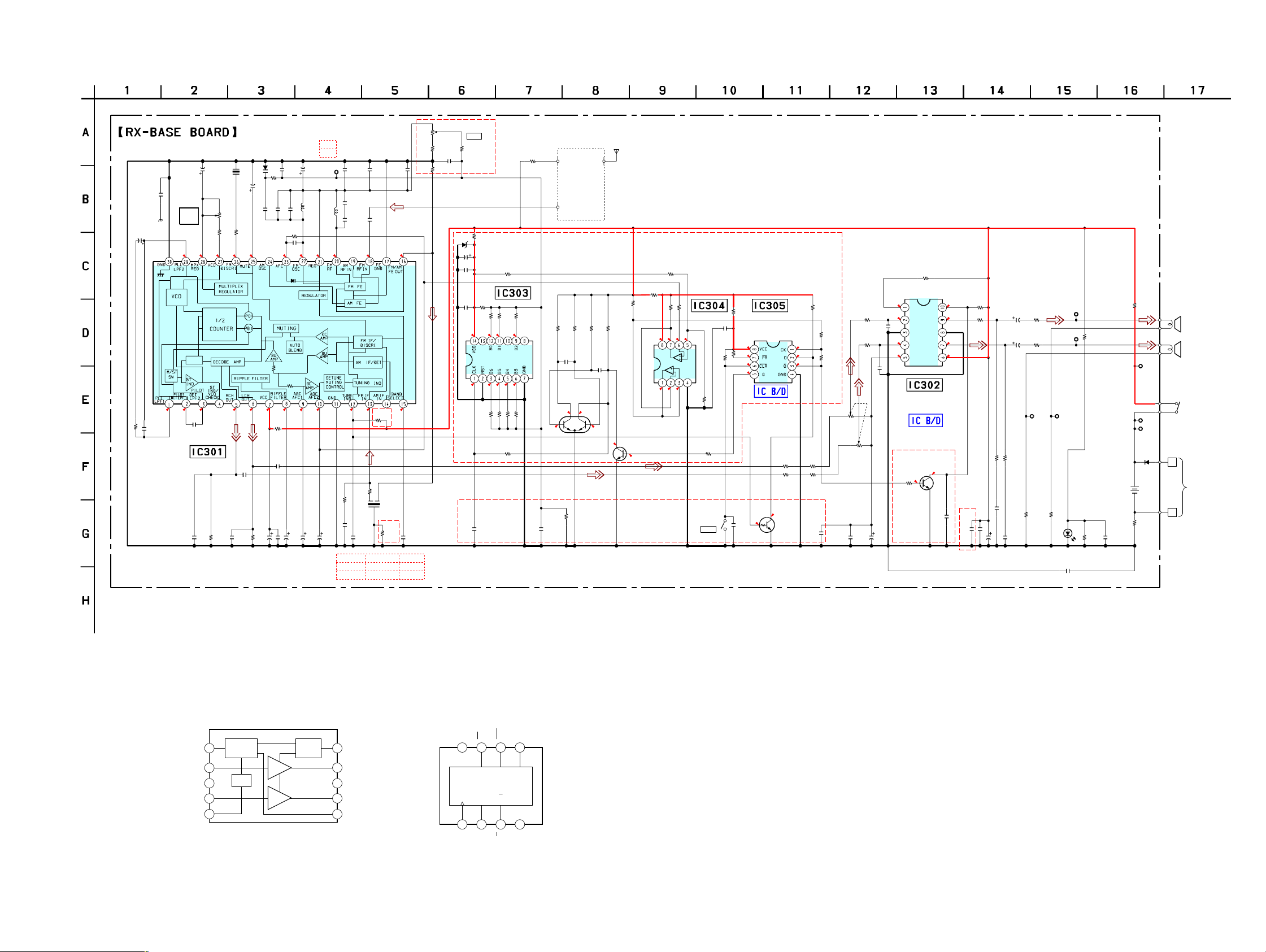
4-2. SCHEMATIC DIAGRAM
C311
10
16V
C366
C303
4.7/16V
R302
2.2k
0.001
CXA1538N-T4
IC301
C302
0.47
0.9
C304
0.022
FREE
RUN
FREQ.
0.9
0.8
C301
IF AMP/DET
RV301
4.7k
R310
3.3k
1.6
0.9
1
R304
3.3k
CF302
10.7MHz
DISC
1.3
C305
0.022
MDR-RF915R/RF845R
RF915R
RV303
R308
C334
10k
TUNE
JC324
1
2.2k
R366
150
D303
UDZ 2.2B
C347
47
16V
C346
0.22
C340
R340
0.1
4.7k
R341
470k
2.0
2.0
IC303
TC74HC4024
0
2.0
RF945R
C337
100p
JC304
COUNTER
R342
240k
2.0
0
7.5k
R347
R348
47k
2.0
15k
R346
R320
10
FE UNIT
(FRONT END)
0
R343
0
2.0
30k
R345
120k
62k
R344
R350
R351
15k
C342
0.01
Q301
FMW1-T-148
OSC
0
0.5
R349
10k
C341
0.1
C333
*
RF915R
D301
HVU363ATRU
C312
3.3
50V
JC311
0
1.0
1.6
0.7
0.7
C351
1
R305
3.3k
C306
C320
0.1
R312
15k
68p
10p
C315
C314
0.01
C313
R309
100k
0
2.1
2.3
R330
10
C350
1
C308
22
16V
C307
0.01
5p
RF945R
3p
C316
10
16V
L301
AIR COIL
C333
*
0
0
1.2
1.2
22
16V
C310
C309
*
C317
C352
0.001
0.001
C336
56p
µH
C332
0.33
L302
0
*
1
50V
150
R326
0.01
C335
RF915R
RF945R
C319
56p
0.01
0
R331
0
2.2k
1.3
RF945R
R325
330
10.7MHz
RF945R
C331
*
C309
2.2 50V
1 50V
CF301
JC302
R323
4.7k
C355
0.001
0
1.3
C329
0
0.01
C331
0.01
1
FM
(ANTENNA)
RF945R
R356
22k
JC303
0
R367
JC306
47k
0
R352
R353
1M
15k
1M
C343
0.01
IC304
0
0.4
0
0.6
2SC2712L
OSC SWITCH
2.4
BA10393F
0.9
Q303
22k
47k
ERROR AMP
R358
R355
1.2
1.0
0
0
R357
0.9
22k
R354
S301
TUNE
R332
1.0k
FF
C345
0.1
IC305
2.3
2.3
2.4
2.3
C344
0.1
0
TC7W74FU
Q305
DTC114TK
BUFFER
JC301
JC305
2.3
R361
22k
22k
R360
22k
R364
22k
R362
10k
0.6
2.3
R363
22k
0
RV302(1/2)
R327
33k
0
R328
0
33k
C367
0.001
(VOLUME)
C364
0.001
RV302(2/2)
C330
2.4
R333
2.2k
1.1
C361
100p
R334
2.2k
0
1.1
C362
100p
AUDIO AMP
IC302
LA4533MTP-1
RF945R
Q304
2SC2712L
AUDIO MUTE
33
16V
R318
2.3
0.1
47k
C323
0.1
R314
100k
2.3
1.1
JC309
0
1.1
2.4
RF915R
0.01
C345
0.01
C357
C324
6.3V
C325
JC331
220
0
6.3V
C326
JC332
220
0
6.3V
R316
10
10
R315
0.1
C327
JC334
JC333
0
0
C328
0.1
220
SLR-342VCTB7
D304
(power)
C365
0.001
RECHARGEABLE
(NICKEL-CADMIUM)
R321
1.5k
BATTERY
NC-AA
2pcs,2.4V
R322
6.8k
C363
0.01
JC336
JC335
0
0
D310
RB411D
N1-CD
+
-
+
-
+
-
SPEAKER
(L-ch)
SPEAKER
(R-ch)
S1
(POWER ON/OFF)
TO
TMR-RF915R/RF945R
(BATTERY
CHARGE
TERMINAL)
• IC BLOCK DIAGRAMS
IC302 LA4533MTP-1
POWER
1
P/SW
IN1
PRE GND
IN2
REF
SWITCH
2
3
4
AMP1
BIAS
AMP2
5
MUTE
CIRCIUT
10
MT/SW
OUT1
9
8
POWER GND
7
OUT2
6
VCC
IC305 TC7W74FU
CLR
PR
VCC
8
1
CK
6
7
RSQ
QDC
3Q2
D
Note on schematic diagrams.
Note:
• All capacitors are in µF unless otherwise noted. pF: µµF 50 WV or
less are not indicated except for electrolytics and tantalums.
• All resistors are in Ω and 1/
• A : B+ Line.
• H : adjustment for repair.
• Power voltage is dc 2.4V and fed with regulated dc power supply
Q
5
from battery terminal.
• Voltages are dc with respect to ground under no-signal conditions.
• Voltages are taken with a VOM (Input impedance 10 MΩ).
• Signal path.
F : FM
L : AUDIO
4
GND
9
9
4
W or less unless otherwise specified.
Page 10

MDR-RF915R/RF845R
4-3. PRINTED WIRING BOARD
1
A
ANT301
RX-BASE BOARD (SIDE A)
2
(ANTENNA)
C309
RF945R
JC302
R325
R326
C335
B
C340
RF945R
R341
R340
CF301
R342
R343
IC303
R308
C
D
RV303
TUNE
RF915R
C337
C341
RF945R
S301
TUNE
E
R347
R349
R346
R345
R323
S301
R344
C334
C316
C344
C320
R312
JC324
D301
L301
JC305
R328
JC301
C332
C315
C336
C313
D304
power
L302
C314
C355
R327
C367
RF945R
3 4 5 6 7
C303
C308
C329
C331
C317
C312
C319
JC335
D310
C306
C307
IC301
C363
R330
R309
C333
C366
Q304
R322
C302
R320
Q305
IC305
R318
JC303
R321
R302
C301
R348
R331
R361
R360
R314
10 6
C365
15
R333
C351
R304
R310
Q303
R354
R362
R363
R364
R332
C323
IC302
C361
C362
C350
C304
R353
R334
C305
C352
C343
JC306
R367
C345
JC309
C364
R355
R305
RF945R
R352
JC304
R358
C357
R316
C328
JC311
Q301
R351
IC304
R315
C330
R366
C327
C311
C342
JC336
C326
JC332
RV301
CF302
R350
R356
R357
C325
JC331
JC334
C310
C346
FE UNIT
(FRONT-END)
C347
D303
C324
JC333
–
SPEAKER
+
–
+
(L-CH)
SPEAKER
(R-CH)
RX-BASE BOARD (SIDE B)
RV302
VOL
w
1-677-934-
RECHAGEABLE BATTERY
+
(NICKEL-CADMIUM)
F
NC-AA
2PCS, 2.4V
–
TO TMR-RF915R/RF945R
(BATTERY CHARGE TERMINAL)
11
(11)
S1
(POWER ON/OFF)
• Semiconductor
Location
Ref. No. Location
D301 C-2
D303 D-5
D304 D-3
D310 E-3
8
1-677-934-
9 10
11
(11)
Note:
• X : parts extracted from the component side.
• a : Through hole.
• : Pattern from the side which enables seeing.
(The other layer's patterns are not indicated.)
Caution:
IC301 B-3
IC302 E-4
IC303 C-2
IC304 D-4
Pattern face side: Parts on the pattern face side seen from the
(Side B) pattern face are indicated.
Parts face side: Parts on the parts face side seen from the
(Side A) parts face are indicated.
IC305 D-4
10
Q301 C-4
Q303 C-4
Q304 D-3
Q305 C-3
10
Page 11

NOTE:
• -XX, -X mean standardized parts, so they may
have some differences from the original one.
• Items marked “*” are not stocked since they
are seldom required for routine service. Some
delay should be anticipated when ordering these
items.
MDR-RF915R/RF945R
SECTION 5
EXPLODED VIEWS
• The mechanical parts with no reference number
in the exploded views are not supplied.
• Hardware (# mark) list and accessories and
packing materials are given in the last of this
parts list.
1
23
26
20
3
2
24
b
a
#2
4
5
#1
#1
6
24
19
26
25
16
26
17
#2
S1
b
a
8
#1
8
#2
10
24
#1
9
22
27
12
21
1415
#2
26
11
26
23
13
9
#1
5
3
4
Ref. No. Part No. Description Remarks Ref. No. Part No. Description Remarks
1 3-046-672-01 SUSPENDER
2 3-046-671-01 BAND, HEAD (RF945R)
2 3-046-671-11 BAND, HEAD (RF915R)
3 3-046-692-01 PAT, EAR
4 1-542-400-11 DRIVER (030F032)
5 3-046-685-01 PLATE (L), FRONT
6 3-046-675-41 HANGER (R) (RF915R:US)
6 3-046-675-51 HANGER (R) (RF915R:CND)
6 3-046-675-61 HANGER (R) (RF945R:US)
6 3-046-675-71 HANGER (R) (RF945R:CND)
8 4-992-281-01 HOLDER, BALL SHAFT
9 4-981-975-01 SPRING, TENSION
* 10 A-3062-556-A RX-BASE BORAD,COMPLETE (RF915R)
* 10 A-3062-564-A RX-BASE BORAD,COMPLETE (RF945R)
11 3-046-677-01 COVER (R), HANGER (RF945R)
11 3-046-677-11 COVER (R), HANGER (RF915R)
12 3-049-799-01 LIGHT, MDR GUIDE
13 3-046-679-41 CAP (R), ORNAMENTAL (RF915R)
13 3-046-679-51 CAP (R), ORNAMENTAL (RF945R)
14 3-046-674-01 HANGER (L) (RF945R)
14 3-046-674-11 HANGER (L) (RF915R)
15 3-048-267-01 TERMINAL (MIDWAY), BATTERY
16 3-048-265-01 TERMINAL (+), BATTERY
17 3-048-266-01 TERMINAL (-), BATTERY
19 3-046-676-01 COVER (L), HANGER (RF945R)
19 3-046-676-11 COVER (L), HANGER (RF915R)
20 3-046-678-41 CAP (L), ORNAMENTAL (RF915R)
20 3-046-678-51 CAP (L), ORNAMENTAL (RF945R)
21 3-046-682-01 TERMINAL, CHARGE
22 3-046-680-01 BUTTON, TUNING (RF945R)
23 3-048-264-01 SHEET, ORNAMENTAL CAP ADHESIVE
24 3-223-909-01 SCREW (B2)
25 1-756-112-31 BATTERY, NICKEL CADMIUM
26 3-224-743-01 SHEET, HOLE (RF945R)
27 3-846-312-01 SPACER
S1 1-771-249-11 SWITCH, PUSH (1 KEY) (POWER ON/OFF)
#1 7-685-104-19 SCREW +P 2X6 TYPE2 NON-SLIT
#2 7-685-105-19 SCREW +P 2X8 TYPE2 NON-SLIT
11
Page 12

MDR-RF915R/RF945R
RX-BASE
Ref. No. Part No. Description Remarks Ref. No. Part No. Description Remarks
NOTE:
• Due to standardization, replacements in the
parts list may be different from the parts
specified in the diagrams or the components
used on the set.
• -XX, -X mean standardized parts, so they
may have some difference from the original
one.
• Items marked “*” are not stocked since they
are seldom required for routine service.
Some delay should be anticipated when
ordering these items.
Ref. No. Part No. Description Remarks Ref. No. Part No. Description Remarks
* A-3062-556-A RX-BASE BOARD, COMPLETE (RF915R)
ELECTRICAL PARTS LIST
• CAPACITORS:
uF: µF
• RESISTORS
All resistors are in ohms.
METAL: metal-film resistor
METAL OXIDE: Metal Oxide-film resistor
F: nonflammable
• COILS
uH: µH
SECTION 6
• SEMICONDUCTORS
In each case, u: µ, for example:
uA...: µA... , uPA... , µPA... ,
uPB... , µPB... , uPC... , µPC... ,
uPD..., µPD...
When indicating parts by reference number,
please include the board name.
C335 1-163-021-91 CERAMIC CHIP 0.01uF 10% 50V
* A-3062-564-A RX-BASE BOARD, COMPLETE (RF945R)
*****************************
3-046-682-01 TERMINAL, CHARGE
< CAPACITOR >
C301 1-164-346-11 CERAMIC CHIP 1uF 16V
C302 1-164-005-11 CERAMIC CHIP 0.47uF 25V
C303 1-124-259-11 ELECT 4.7uF 20% 16V
C304 1-163-037-11 CERAMIC CHIP 0.022uF 10% 25V
C305 1-163-037-11 CERAMIC CHIP 0.022uF 10% 25V
C306 1-124-234-00 ELECT 22uF 20% 16V
C307 1-163-059-91 CERAMIC CHIP 0.01uF 10% 50V
C308 1-124-234-00 ELECT 22uF 20% 16V
C309 1-104-942-11 ELECT 1uF 20% 50V
(RF945R)
C309 1-124-257-00 ELECT 2.2uF 20% 50V
(RF915R)
C310 1-104-942-11 ELECT 1uF 20% 50V
C311 1-124-233-11 ELECT 10uF 20% 16V
C312 1-126-162-11 ELECT 3.3uF 20% 50V
C313 1-163-021-91 CERAMIC CHIP 0.01uF 10% 50V
C314 1-164-441-11 CERAMIC CHIP 68PF 5% 50V
C315 1-163-227-11 CERAMIC CHIP 10PF 0.50PF 50V
C316 1-124-233-11 ELECT 10uF 20% 16V
C317 1-163-009-11 CERAMIC CHIP 0.001uF 10% 50V
C319 1-163-021-91 CERAMIC CHIP 0.01uF 10% 50V
C320 1-163-038-00 CERAMIC CHIP 0.1uF 25V
C323 1-163-038-00 CERAMIC CHIP 0.1uF 25V
(RF945R)
C324 1-124-635-00 ELECT 220uF 20% 6.3V
C325 1-124-635-00 ELECT 220uF 20% 6.3V
C326 1-124-635-00 ELECT 220uF 20% 6.3V
C327 1-163-038-91 CERAMIC CHIP 0.1uF 25V
C336 1-163-245-11 CERAMIC CHIP 56PF 5% 50V
C337 1-163-251-11 CERAMIC CHIP 100PF 5% 50V
(RF945R)
C340 1-163-038-00 CERAMIC CHIP 0.1uF 25V
(RF945R)
C341 1-163-038-00 CERAMIC CHIP 0.1uF 25V
(RF945R)
C342 1-163-021-91 CERAMIC CHIP 0.01uF 10% 50V
(RF945R)
C343 1-163-021-91 CERAMIC CHIP 0.01uF 10% 50V
(RF945R)
C344 1-163-038-00 CERAMIC CHIP 0.1uF 25V
(RF945R)
C345 1-163-021-91 CERAMIC CHIP 0.01uF 10% 50V
(RF915R)
C345 1-163-038-00 CERAMIC CHIP 0.1uF 25V
(RF945R)
C346 1-164-489-11 CERAMIC CHIP 0.22uF 10% 16V
(RF945R)
C347 1-124-589-11 ELECT 47uF 20% 16V
(RF945R)
C350 1-164-346-11 CERAMIC CHIP 1uF 16V
C351 1-164-346-11 CERAMIC CHIP 1uF 16V
C352 1-163-009-11 CERAMIC CHIP 0.001uF 10% 50V
C355 1-163-009-11 CERAMIC CHIP 0.001uF 10% 50V
C357 1-163-021-91 CERAMIC CHIP 0.01uF 10% 50V
C361 1-163-251-11 CERAMIC CHIP 100PF 5% 50V
C362 1-163-251-11 CERAMIC CHIP 100PF 5% 50V
C363 1-163-021-91 CERAMIC CHIP 0.01uF 10% 50V
C364 1-163-009-11 CERAMIC CHIP 0.001uF 10% 50V
C365 1-163-009-11 CERAMIC CHIP 0.001uF 10% 50V
C366 1-163-009-11 CERAMIC CHIP 0.001uF 10% 50V
C367 1-163-009-11 CERAMIC CHIP 0.001uF 10% 50V
(RF945R)
C328 1-163-038-91 CERAMIC CHIP 0.1uF 25V
C329 1-163-021-91 CERAMIC CHIP 0.01uF 10% 50V
C330 1-124-242-00 ELECT 33uF 20% 25V
C331 1-163-021-91 CERAMIC CHIP 0.01uF 10% 50V
C331 1-164-346-11 CERAMIC CHIP 1uF 16V
C332 1-163-245-11 CERAMIC CHIP 56PF 5% 50V
C333 1-163-220-11 CERAMIC CHIP 3PF 0.25PF 50V
C333 1-163-222-11 CERAMIC CHIP 5PF 0.25PF 50V
C334 1-164-346-11 CERAMIC CHIP 1uF 16V
12
(RF915R)
(RF945R)
(RF945R)
(RF915R)
(RF915R)
< CERAMIC FILTER >
CF301 1-577-588-11 FILTER, CERAMIC
CF302 1-577-572-11 FILTER, CERAMIC
< DIODE >
D301 8-719-083-90 DIODE HVU363ATRU
D303 8-719-056-71 DIODE UDZ-TE-17-2.2B (RF945R)
D304 8-719-077-16 LED TLSU124(TPJ52) (power)
D310 8-719-975-40 DIODE RB411D
< IC >
IC301 8-752-072-12 IC CXA1538N
IC302 8-759-802-75 IC LA4533MTP
Page 13

MDR-RF915R/RF945R
RX-BASE
Ref. No. Part No. Description Remarks Ref. No. Part No. Description Remarks
IC303 8-759-453-43 IC TC74HC4024AF (RF945R)
IC304 8-759-510-73 IC BA10393F-E2 (RF945R)
IC305 8-759-083-94 IC TC7W74FU (RF945R)
< JUMPER RESISTOR >
JC301 1-216-295-91 SHORT 0
JC302 1-216-295-91 SHORT 0 (RF945R)
JC303 1-216-295-91 SHORT 0
JC304 1-216-295-91 SHORT 0 (RF945R)
JC305 1-216-295-91 SHORT 0
JC306 1-216-295-91 SHORT 0 (RF945R)
JC309 1-216-295-91 SHORT 0
JC311 1-216-295-91 SHORT 0
JC324 1-216-295-91 SHORT 0 (RF915R)
JC331 1-216-295-91 SHORT 0
JC332 1-216-295-91 SHORT 0
JC333 1-216-295-91 SHORT 0
JC334 1-216-295-91 SHORT 0
JC335 1-216-295-91 SHORT 0
JC336 1-216-295-91 SHORT 0
< COIL >
L301 1-422-317-31 COIL, AIR-CORE
L302 1-412-933-11 INDUCTOR 0.33uH
< TRANSISTOR >
Q301 8-729-903-10 TRANSISTOR FMW1-T-148 (RF945R)
Q303 8-729-200-72 TRANSISTOR 2SC2712L-TE85L (RF945R)
Q304 8-729-200-72 TRANSISTOR 2SC2712L-TE85L (RF945R)
Q305 8-729-027-44 TRANSISTOR DTC114TKA-T146 (RF945R)
< RESISTOR >
R302 1-216-057-00 METAL CHIP 2.2K 5% 1/10W
R304 1-216-061-00 RES-CHIP 3.3K 5% 1/10W
R305 1-216-061-00 RES-CHIP 3.3K 5% 1/10W
R308 1-216-057-00 METAL CHIP 2.2K 5% 1/10W
R309 1-216-097-11 RES-CHIP 100K 5% 1/10W
R341 1-216-113-00 METAL CHIP 470K 5% 1/10W
(RF945R)
R342 1-216-106-00 METAL CHIP 240K 5% 1/10W
(RF945R)
R343 1-216-099-00 METAL CHIP 120K 5% 1/10W
(RF945R)
R344 1-216-092-00 RES-CHIP 62K 5% 1/10W
(RF945R)
R345 1-216-084-00 METAL CHIP 30K 5% 1/10W
(RF945R)
R346 1-216-077-00 RES-CHIP 15K 5% 1/10W
(RF945R)
R347 1-216-070-00 METAL CHIP 7.5K 5% 1/10W
(RF945R)
R348 1-216-089-91 RES-CHIP 47K 5% 1/10W
(RF945R)
R349 1-216-073-00 RES-CHIP 10K 5% 1/10W
(RF945R)
R350 1-216-077-00 RES-CHIP 15K 5% 1/10W
(RF945R)
R351 1-216-121-11 RES-CHIP 1M 5% 1/10W
(RF945R)
R352 1-216-121-11 RES-CHIP 1M 5% 1/10W
(RF945R)
R353 1-216-077-00 RES-CHIP 15K 5% 1/10W
(RF945R)
R354 1-216-081-00 METAL CHIP 22K 5% 1/10W
(RF945R)
R355 1-216-089-91 RES-CHIP 47K 5% 1/10W
(RF945R)
R356 1-216-081-00 METAL CHIP 22K 5% 1/10W
(RF945R)
R357 1-216-081-00 METAL CHIP 22K 5% 1/10W
(RF945R)
R358 1-216-081-00 METAL CHIP 22K 5% 1/10W
(RF945R)
R360 1-216-081-00 METAL CHIP 22K 5% 1/10W
(RF945R)
R361 1-216-081-00 METAL CHIP 22K 5% 1/10W
(RF945R)
R310 1-216-061-00 RES-CHIP 3.3K 5% 1/10W
R312 1-216-077-00 RES-CHIP 15K 5% 1/10W
R314 1-216-097-11 RES-CHIP 100K 5% 1/10W
R315 1-216-001-00 METAL CHIP 10 5% 1/10W
R316 1-216-001-00 METAL CHIP 10 5% 1/10W
R318 1-216-089-91 RES-CHIP 47K 5% 1/10W
(RF945R)
R320 1-216-001-00 METAL CHIP 10 5% 1/10W
R321 1-216-053-00 METAL CHIP 1.5K 5% 1/10W
R322 1-216-069-00 METAL CHIP 6.8K 5% 1/10W
R323 1-216-065-91 RES-CHIP 4.7K 5% 1/10W
(RF915R)
R325 1-216-037-00 METAL CHIP 330 5% 1/10W
R326 1-216-029-00 METAL CHIP 150 5% 1/10W
R327 1-216-085-00 RES-CHIP 33K 5% 1/10W
R328 1-216-085-00 RES-CHIP 33K 5% 1/10W
R330 1-216-001-00 METAL CHIP 10 5% 1/10W
R331 1-216-057-00 METAL CHIP 2.2K 5% 1/10W
(RF945R)
R332 1-216-049-11 RES-CHIP 1K 5% 1/10W
(RF945R)
R333 1-216-057-00 METAL CHIP 2.2K 5% 1/10W
R334 1-216-057-00 METAL CHIP 2.2K 5% 1/10W
R340 1-216-071-00 METAL CHIP 8.2K 5% 1/10W
(RF945R)
R362 1-216-073-00 RES-CHIP 10K 5% 1/10W
R363 1-216-081-00 METAL CHIP 22K 5% 1/10W
R364 1-216-081-00 METAL CHIP 22K 5% 1/10W
R366 1-216-029-00 METAL CHIP 150 5% 1/10W
R367 1-216-089-91 RES-CHIP 47K 5% 1/10W
< VARIABLE RESISTOR >
RV301 1-241-763-11 RES, ADJ, CARBON 4.7K (FREE RUN FREQ.)
RV302 1-227-189-11 RES, VAR CARBON 20K/20K (VOL )
RV303 1-227-190-11 RES, VAR CARBON 10K (TUNE) (RF915R)
< SWITCH >
S301 1-771-980-11 SWITCH, TACTILE (TUNE) (RF945R)
(RF945R)
(RF945R)
(RF945R)
(RF945R)
(RF945R)
w
******************************************************
MISCELLANEOUS
*************
4 1-542-400-11 DRIVER (030F032)
25 1-756-112-31 BATTERY, NICKEL CADMIUM
S1 1-771-249-11 SWITCH, PUSH (1 KEY) (POWER ON/OFF)
13
Page 14

MDR-RF915R/RF945R
REVISION HISTORY
Clicking the version allows you to jump to the revised page.
Also, clicking the version at the upper right on the revised page allows you to jump to the next revised
page.
Ver. Date Description of Revision
1.0 2001.05 New
Page 15

MDR-RF915RK/RF945RK
SERVICE MANUAL
Ver 1.0 2001. 05
Photo : MDR-RF945RK
MDR-RF915RK and MDR-RF945RK are Composed of the following
models.
As for the service manual it is issued for each component model,
then please refer to it.
COMPONENT MODEL NAME FOR MDR-RF915RK/
MDR-RF945RK
MDR-RF915RK MDR-RF945RK
Wireless Stereo Headphones MDR-RF915R MDR-RF945R
Transmitter TMR-RF915R TMR-RF945R
PARTS LIST
The components identified by
mark ! or dotted line with mark
! are critical for safety.
Replace only with part number
specified.
Ref. No. Part No. Description Remark
0 1-473-588-12 ADAPTOR, AC (AC-S901)
1-473-606-11 ADAPTOR, PLUG
1-751-754-11 CORD, CONNECTION
3-233-607-11 MANUAL, INSTRUCTION
3-233-607-21 MANUAL, INSTRUCTION (ENGLISH, FRENCH)
Les composants identifiés par une
marque ! sont critiques pour
la sécurité.
Ne les remplacer que par une pièce
portant le numéro spécifié.
ACCESSORIES & PACKING MATERIALS
****************************
(Stereo mini jack t stereo phone plug)
(Phono plugs y stereo mini plug), 1m
(ENGLISH, SPANISH) (US)
(Canadian)
US Model
Canadian Model
SPECIFICATIONS
General
Carrier frequency
913.5 – 914.5 MHz
Channel Ch1, Ch2, Ch3
Modulation FM stereo
Frequency response
20 – 20,000 Hz
Transmitter TMR-RF945R, TMR-RF915R
Power source DC 9 V: supplied AC power adaptor
Audio input phono jacks/stereo mini jack
Dimensions Approx. 150 mm dia. 108 mm
Mass Approx. 190 g (6.7 oz.)
Headphones MDR-RF945R, MDR-RF915R
Power source DC 2.4 V: Built-in rechargeable
Mass Approx. 240 g (8.5 oz.) incl.
Built-in Ni-Cd rechargeable battery
Model name NC-AA
Voltage 1.2 V
Capacity 700 mAh
Design and specifications are subject to change without
notice.
1
(6 4 x
built-in rechargeable battery
in.) (w/h)
/
3
battery
x
9-873-138-11
2001E0200-1
© 2001.5
WIRELESS STEREO
HEADPHONE SYSTEM
Sony Corporation
Personal Audio Company
Shinagawa Tec Service Manual Production Group
Page 16

MDR-RF915RK/RF945RK
f
Setting up the
transmitter
1
Connect the transmitter to audio/video
equipment. Select one of the hookups
below depending on the jack type:
To connect to a headphones jack
A
SECTION 1
GENERAL
5
- Turn up the volume to a moderate
This section is extracted from
instruction manual.
A
level with the VOL control.
Press the TUNING button briefly for
automatic tuning of the headphones.
If you do not receive a clear audio
signal, press it again.
A
MDR-RF945RK
Transmitter
OFF ON
FILTERNOISE
Right channel
(red)
Connecting cord
(supplied)
Unimatch plug
adaptor
(supplied)
to headphones
jack (stereo
phone jack)
RBAL
AUDIO IN
to AUDIO IN
A jacks
DC IN 9V
123
CHANNEL
Left channel
(white)
to headphones
jack (stereo
mini jack)
Discman, MD,
WALKMAN*, VCR,
etc.
TUNING
button
VOL control
B
5
- Turn up the volume to a moderate
level with the VOL control, then tune
the headphones in to the frequency o
the transmitter with the TUNING
control until you can hear the audio
signal loud and clear.
MDR-RF915RK
B
TUNING
control
VOL control
Try the above steps 3 and 5 until the
receiving performance becomes better.
Auto power on/off function
When you remove the headphones from your
head, the power turns off automatically. Do not
allow the self adjusting band to be pulled up,
otherwise the headphones will be switched on.
The power turns on.
2
Page 17

MDR-RF915RK/RF945RK
3
Page 18

MDR-RF915RK/RF945RK
REVISION HISTORY
Clicking the version allows you to jump to the revised page.
Also, clicking the version at the upper right on the revised page allows you to jump to the next revised
page.
Ver. Date Description of Revision
1.0 2001.05 New
Page 19

TMR-RF915R/RF945R
SERVICE MANUAL
Ver 1.0 2001. 05
Photo : TMR-RF945R
TMR-RF915R is the component model block one in the MDR-RF915RK.
TMR-RF945R is the component model block one in the MDR-RF945RK.
COMPONENT MODEL NAME FOR MDR-RF915RK/
MDR-RF945RK
MDR-RF915RK MDR-RF945RK
Wireless Stereo Headphones MDR-RF915R MDR-RF945
Transmitter TMR-RF915R TMR-RF945
US Model
Canadian Model
SPECIFICATIONS
General
Carrier frequency
913.5 – 914.5 MHz
Channel Ch1, Ch2, Ch3
Modulation FM stereo
Frequency response
20 – 20,000 Hz
Transmitter
Power source DC 9 V: supplied AC power
adaptor
Audio input phono jacks/stereo mini jack
Dimensions Approx. 150 mm dia X 108 mm
(6 X 41/3 in.) (w/h)
Mass Approx. 190 g (6.7 oz.)
Design and specifications are subject to change without
notice.
TRANSMITTER
9-873-139-11
2001E0200-1
© 2001.5
Sony Corporation
Personal Audio Company
Shinagawa Tec Service Manual Production Group
Page 20

TMR-RF915R/RF945R
SECTION 1
GENERAL
TABLE OF CONTENTS
Specifications ............................................................................ 1
1. GENERAL ...................................................................... 2
2. DISASSEMBLY
2-1. Cabinet (Upper) ........................................................ 3
2-2. TX-BASE Board ....................................................... 3
3. ELECTRICAL ADJUSTMENTS ............................. 4
4. DIAGRAMS
4-1. Block Diagrams ......................................................... 5
4-2. Schematic Diagram ................................................... 6
4-3. Printed Wiring Board ................................................ 7
5. EXPLODED VIEWS..................................................... 8
6. ELECTRICAL PARTS LIST...................................... 9
This section is extracted from
instruction manual.
Setting up the
transmitter
1
Connect the transmitter to audio/video
equipment. Select one of the hookups
below depending on the jack type:
To connect to a headphones jack
A
Transmitter
OFF ON
FILTERNOISE
Right channel
(red)
RBAL
AUDIO IN
DC IN 9V
Left channel
(white)
to AUDIO IN
A jacks
123
CHANNEL
SAFETY CHECK-OUT
After correcting the original service problem, perform the following
safety checks before releasing the set to the customer.
1. Check the area of your repair for unsoldered or poorly-sol
deredconnections. Check the entire board surface for solder
splashes and bridges.
2. Check the interboard wiring to ensure that no wires are
“pinched” or contact high-wattage resistors.
3. Look for unauthorized replacement parts, particularlyt ransis
tors, that were installed during a previous repair.
Point them out to the customer and recommend their
replacement.
4. Look for parts which, through functioning, show obvious
signs of deterioration. Point them out to the customer and
recommend their replacement.
Connecting cord
(supplied)
Unimatch plug
adaptor
(supplied)
to headphones
jack (stereo
phone jack)
5. Check the B+ voltage to see it is at the values specified.
6. Flexible Circuit Board Repairing
• Keep the temperature of the soldering iron around 270°C
during repairing.
• Do not touch the soldering iron on the same conductor of
the circuit board (within 3 times).
• Be careful not to apply force on the conductor when
soldering
to headphones
jack (stereo
mini jack)
Discman, MD,
WALKMAN*, VCR,
etc.
2
Page 21

• This set can be disassembled in the order shown below.
)
r
2-1. CABINET (UPPER)
TMR-RF915R/RF945R
SECTION 2
DISASSEMBLY
2
Cabinet (upper)
1
Four screws (P 2
× 8
2-2. TX-BASE BOARD
2
TX-BASE board
Cabinet assy, lowe
1
3
Page 22

TMR-RF915R/RF945R
t
SECTION 3
ELECTRICAL ADJUSTMENTS
Setting :
AF signal
generator
set
TMR-RF915R/RF945R
L-CH (J402)
Telescopic
antenna
Frequency counter
8 cm
TMR-RF915R/RF945R
set
Transmission Frequency Check
1. Set the noise filter SW to OFF.
2. Input a signal of 1 kHz 40 mVrms to only the L-CH (J402).
3. Connect a telescopic antenna to the frequency counter input
and extend the antenna to a length of approximately 8 cm.
4. Place TX-BASE board close to the frequency counter, then measure the frequencies of CH1, CH2 and CH3 and make sure the
values are as follows:
CH1 : 913.5 MHz ± 200 kHz
CH2 : 914.0 MHz ± 200 kHz
CH3 : 914.5 MHz ± 200 kHz
Pilot signal Modulation Check and Adjustment
1. Set the channel to CH2.
2. An electric wave is output for 5or 10 minutes when OFF to ON a
power supply (Power indicator will ON).
3. Measure the center terminal of RV403 using an digital volt-meter
(AC range) and make sure the value is 2 to 2.5mVrms.
If the measured value is other than the specified value, adjust to
2 to 2.5mVrms by turning the RV403 on the TX-BASE board.
Connection points and Adjustment Location :
TX-BASE BOARD
←
CH2 ←CH1
CH3
S402
RV403
(Component side)
(L-CH) (R-CH)
J402
VCO UNIT
Hole
When the frequency is not satisfied the specified value, set the
channel switch (S402) to CH2, then adjust the value of the
frequency counter to 914.0 MHz by trimmer capacitor in the VCO
unit.
Standard value :913.9MHz to 914.1MHz
When completed with replacement, recheck the
frequencies of CH1, CH2 and CH3.
RV403: Modulation adjustment
TX-BASE BOARD
digtal voltmeter
(AC range)
C470
O401
UNIT)
(Conductor side)
417
420
JW
JW
R482
C439
R449
Trimmer : Transmission
C480
D403
R485
416
JW
R486
R483
RV403
R464
JC470
58
frequency adjustmen
R484
IC402
413
JW
R472
1
2
3
R466
JC430
C468
Q404
C475
JW
R481
415
Q408
R489
4
Page 23

4-1. BLOCK DIAGRAMS
TX-BASE BOARD
SECTION 4
DIAGRAMS
TMR-RF915R/RF945R
B
AUDIO IN
A
J401
J402
L
R R-CH
R-CH
S401
NOISE FILTER
OFF
|
ON
NOISE
FILTER
IC401
ALC
AMP
LPF
R-CH
IC403
STEREO MPX
CH1
1 9
AMP
CH2
14
AMP
TIME
DEVISION
MPX
BUFFER
OSC
AMP
X401
38kHz
BUFFER
DIVIDER
76
8
B+
5V
RV403
MODULATION
CHANNEL
SET
Q408
1
2
3
S402
CHANNEL
ANT401
ANT
MOD IN
I
VCO401
(VCO UNIT)
O
B+
5V
V
5V
IC402
+5V
REG
D401
POWER
SWITCH
Q404
POWER
ON/OFF
Q406,407
D402
CHG
J404
DC IN 9V
+
–
CHARGE
TERMINAL
(TO MDR-RF915R/RF945R)
• R-ch is omitted due to same as L-ch.
• Signal path.
L : AUDIO
F : FM
BUFFER
Q401
RECT
D404,405
Q402,405
INPUT
DET
5
5
Page 24

TMR-RF915R/RF945R
4-2. SCHEMATIC DIAGRAM • See page 7 for Notes.
AUDIO IN
JW407
J401
B
J402
R
A
L
R411
33k
R401
33k
R414
33k
JW401
JW402
R404
33k
S401
NOISE FILTER
OFF
ON
R446
1.2k
C432
0.0056
R406
33k
R403
19KLPF
51
L408
JC404
JC405
0
0
R416
33k
R407
R413
51
R418
2.2k
R408
2.2k
C413
0.001
R417
R457
4.7k
R448
1k
R449
22k
1k
1k
C433
1
C403
0.001
IC403
NJM2035M
MPX
JW404
0.022
C416
R423
220
C417
2.2
50V
R421
100k
R422
3.3k
L402
L401
C431
10
16V
R424
3.3M
C469
0.1
C421
22
16V
C458
10
16V
L405
C423
R481
5.6k
100p
C422
220
16V
R429
IC401
BA3308F
ALC
R425
100k
C441
10
16V
R430
10k
R469
180k
C457
330p
R426
3.3k
10k
JW405
JW403
R428
680
C406
0.022
R427
220
C407
2.2
50V
C426
0.01
D408
MTZ-77-2.0B
C466
0.01
JC470
C451
JC430
0
2SC2712L
220
16V
0
R432
2.2M
R431
4.7k
C425
0.022
C428
100p
Q401
C427
0.01
R440
R433
22k
1k
R441
1.8k
R472
470
Q401,402
AUDIO INPUT
C430
4.7
16V
D404
1SS133T
C429
100p
DET
D405
1SS133T
C444
100p
C445
100p
R438
220k
R452
22k
2SC2712L
C436
10
16V
Q408
DTA124KA
CHANNEL
SET
R453
680k
Q402
R454
47k
Q405-407
POWER ON/OFF
Q405
KTA1266-GR
D410
MA77
Q407
2SC2712L
0.0033
C452
100
16V
C478
JW413
Q406
2SC2712L
D409
MA77
R455
1k
VCO401
914MHZ
VCO UNIT
JW410
R466
22k
JW409
D406
RD5.1ES
L410
R467
4.7k
Q404
KTA1266-GR
POWER
SWITCH
R489
18k
D401
SLR342VCT7
power
R473
620
0.1
C475
C468
0.01
+5V REG
JW411
IC402
KIA78S05
ANT401
(ANTENNA)
CHARGE
TERMINAL
TO
MDR-RF915R/
RF945R
J404
DC IN 9V
RV403
MODULATION
L409
19KLPF
JC403
R474
620
0
R458
1k
R461
4.7k
SLR342MGT
R459
D402
X401
C454
100p
C462
R479
1.2k
10
R478
1.2k
C453
16V
R477
1.2k
100p
R476
1.2k
R475
1.2k
C443
1
22k
chg
38K
C455
10p
C442
0.0056
R456
1.2k
+
–
D403
11ES2-TA1B
JW416
C480
0.01
RV403
4.7k
R464
1k
R465
22k
R484
1.3k
R485
1.2k
C439
R483
2.2k
R486
18k
C440
100p
C483
2p
JW415
1
C470
47
16V
S402
R482
22k
CHANNEL
3
2
1
6
6
Page 25

4-3. PRINTED WIRING BOARD
TMR-RF915R/RF945R
A
B
BATTERY CHARGE
TERMINAL
(TO MDR-RF915R
/RF945R)
C
D
E
1
2
3 4 5
ANT401
ANTENNA
DC IN 9V
JW417
R464
C433
R475
JC403
J404
C469
IC403
C462
C453
D403
JW416
RV403
C454
R467
C480
R485
R486
R483
JC470
C458
C457
X401
C455
JW411
S402
CHANNEL
1t2t3
JW415
JW413
Q408
R481
R469
C451
11
(11)
R484
IC402
1
2
3
R472
JC430
JW412
D408
Q404
R466
C468
C475
R489
• Semiconductor
Location
Ref. No. Location
D401 E-4
D402 E-4
D403 B-4
D404 E-2
D405 E-3
D406 D-3
D408 D-5
D409 D-4
D410 D-4
IC401 C-2
IC402 B-5
IC403 D-4
Q401 D-2
Q402 D-3
Q404 C-5
Q405 D-3
Q406 D-4
Q407 D-3
Q408 C-5
Note:
• X : parts extracted from the component side.
• : Pattern from the side which enables seeing.
Note on schematic diagrams.
Note:
• All capacitors are in µF unless otherwise noted. pF: µµF 50 WV or
less are not indicated except for electrolytics and tantalums.
• All resistors are in Ω and 1/
• A : B+ Line.
• H : adjustment for repair.
• Power voltage is dc 9V and fed with regulated dc power supply
from external power voltage jack.
• Voltages are dc with respect to ground under no-signal conditions.
• Voltages are taken with a VOM (Input impedance 10 MΩ).
• Signal path.
F : FM
L : AUDIO
4
W or less unless otherwise specified.
AUDIO IN
TX-BASE BOARD
S401
J401
B A
R
J402
L
NOISE FILTER
OFF
TON
R403
R413
JW401
C416
R423
R414
R407
R417
R404
C413
JW402
L402
R418
R406
L401
R416
C403
R411
R401
R408
C483
C407
L410
C470
JW420
IC401
C440
Q405
R453
Q407
R479
O
V
I (TP12)
R457
R461
JW410
D401
power
D402
chg
VCO401
(VCO UNIT)
R448
C452
C478
Q406
R473
R478
R474
R482
C439
R449
D410
D409
R476
R458
R459
C443
R477
JW409
R422
–
+
C426
C425
R429
R431
C427
C417
R421
Q401
C429
C466
JW404
C431
R430
JC405
C421
C428
R424
C422
JC404
R433
R432
C430
C423
R428
C445
L405
JW405
R440
C444
D404
R446
R456
D405
JW403
C441
L408
L409
C436
C442
R452
R438
R427
R426
C406
R425
C432
R455
Q402
JW407
R454
D406
R441
R465
1-682-266-
7
7
Page 26

TMR-RF915R/RF945R
SECTION 5
EXPLODED VIEWS
NOTE:
• -XX, -X mean standardized parts, so they may
have some differences from the original one.
• Items marked “*” are not stocked since they
are seldom required for routine service. Some
delay should be anticipated when ordering these
items.
3
• The mechanical parts with no reference number
in the exploded views are not supplied.
• Hardware (# mark) list and accessories and
packing materials are given in the last of this
parts list.
1
2
8
7
#1
4
5
#1
6
Ref. No. Part No. Description Remarks Ref. No. Part No. Description Remarks
1 3-046-687-41 CABINET (UPPER) (RF915R)
1 3-046-687-51 CABINET (UPPER) (RF945R)
2 3-049-800-01 CUSHION, ANTENNA
3 3-046-690-01 TUBE, LIGHT GUIDE
* 4 A-3062-560-A TX-BASE MOUNTED PC BORAD (A)
5 X-3380-840-1 CABINET ASSY, LOWER (RF915R:US)
5 X-3380-841-1 CABINET ASSY, LOWER (RF945R:US)
#1
5 X-3380-846-1 CABINET ASSY, LOWER (RF915R:CND)
5 X-3380-847-1 CABINET ASSY, LOWER (RF945R:CND)
6 4-984-729-01 FOOT, RUBBER
7 3-046-689-01 TERMINAL, CHARGE
8 4-213-164-01 TERMINAL, ANTENNA
#1 7-685-105-19 SCREW +P 2X8 TYPE2 NON-SLIT
8
Page 27

TMR-RF915R/RF945R
SECTION 6
Ref. No. Part No. Description Remarks Ref. No. Part No. Description Remarks
NOTE:
• Due to standardization, replacements in the
parts list may be different from the parts
specified in the diagrams or the components
used on the set.
• -XX, -X mean standardized parts, so they
may have some difference from the original
one.
• Items marked “*” are not stocked since they
are seldom required for routine service.
Some delay should be anticipated when
ordering these items.
Ref. No. Part No. Description Remarks Ref. No. Part No. Description Remarks
* A-3062-560-A TX-BASE BOARD, COMPLETE
ELECTRICAL PARTS LIST
• CAPACITORS:
uF: µF
• RESISTORS
All resistors are in ohms.
METAL: metal-film resistor
METAL OXIDE: Metal Oxide-film resistor
F: nonflammable
• COILS
uH: µH
C478 1-164-182-11 CERAMIC CHIP 0.0033uF 10% 50V
• SEMICONDUCTORS
In each case, u: µ, for example:
uA...: µA... , uPA... , µPA... ,
uPB... , µPB... , uPC... , µPC... ,
uPD..., µPD...
When indicating parts by reference number,
please include the board name.
*********************
3-046-689-01 TERMINAL, CHARGE
C480 1-163-021-91 CERAMIC CHIP 0.01uF 10% 50V
C483 1-163-219-00 CERAMIC CHIP 2PF 50V
TX-BASE
< CAPACITOR >
C403 1-163-009-11 CERAMIC CHIP 0.001uF 10% 50V
C406 1-163-037-11 CERAMIC CHIP 0.022uF 10% 25V
C407 1-126-961-11 ELECT 2.2uF 20% 50V
C413 1-163-009-11 CERAMIC CHIP 0.001uF 10% 50V
C416 1-163-037-11 CERAMIC CHIP 0.022uF 10% 25V
C417 1-126-961-11 ELECT 2.2uF 20% 50V
C421 1-124-234-00 ELECT 22uF 20% 16V
C422 1-126-934-11 ELECT 220uF 20% 16V
C423 1-163-251-11 CERAMIC CHIP 100PF 5% 50V
C425 1-163-037-11 CERAMIC CHIP 0.022uF 10% 25V
C426 1-163-021-91 CERAMIC CHIP 0.01uF 10% 50V
C427 1-163-021-91 CERAMIC CHIP 0.01uF 10% 50V
C428 1-163-251-11 CERAMIC CHIP 100PF 5% 50V
C429 1-163-251-11 CERAMIC CHIP 100PF 5% 50V
C430 1-124-259-11 ELECT 4.7uF 20% 16V
C431 1-126-157-11 ELECT 10uF 20% 16V
C432 1-163-018-00 CERAMIC CHIP 0.0056uF 5% 50V
C433 1-164-346-11 CERAMIC CHIP 1uF 16V
C436 1-126-157-11 ELECT 10uF 20% 16V
C439 1-164-346-11 CERAMIC CHIP 1uF 16V
C440 1-163-251-11 CERAMIC CHIP 100PF 5% 50V
C441 1-126-157-11 ELECT 10uF 20% 16V
C442 1-163-018-00 CERAMIC CHIP 0.0056uF 5% 50V
C443 1-164-346-11 CERAMIC CHIP 1uF 16V
C444 1-163-251-11 CERAMIC CHIP 100PF 5% 50V
C445 1-163-251-11 CERAMIC CHIP 100PF 5% 50V
C451 1-126-934-11 ELECT 220uF 20% 16V
C452 1-126-933-11 ELECT 100uF 20% 16V
C453 1-126-157-11 ELECT 10uF 20% 16V
C454 1-163-251-11 CERAMIC CHIP 100PF 5% 50V
C455 1-163-227-11 CERAMIC CHIP 10PF 0.50PF 50V
C457 1-163-003-11 CERAMIC CHIP 330PF 10% 50V
C458 1-126-157-11 ELECT 10uF 20% 16V
C462 1-163-251-11 CERAMIC CHIP 100PF 5% 50V
C466 1-163-021-91 CERAMIC CHIP 0.01uF 10% 50V
C468 1-163-021-91 CERAMIC CHIP 0.01uF 10% 50V
C469 1-163-038-00 CERAMIC CHIP 0.1uF 25V
C470 1-126-786-11 ELECT 47uF 20% 16V
C475 1-163-038-00 CERAMIC CHIP 0.1uF 25V
< DIODE >
D401 8-719-059-98 LED SLR-342VC3F (power)
D402 8-719-048-87 LED SLR-332MGTB7 (chg)
D403 8-719-200-82 DIODE 11ES2
D404 8-719-991-33 DIODE 1SS133T-77
D405 8-719-991-33 DIODE 1SS133T-77
D406 8-719-109-85 DIODE RD5.1ESB2
D408 8-719-109-51 DIODE RD2.0ESB2
D409 8-719-421-40 DIODE MA77
D410 8-719-421-40 DIODE MA77
< IC >
IC401 8-759-998-71 IC BA3308F
IC402 8-759-537-90 IC KIA78S05P-TP
IC403 8-759-667-59 IC NJM2035M(TE2)
< JACK >
J401 1-566-822-51 JACK (AUDIO IN (K))
J402 1-580-441-61 JACK, PIN 2P (AUDIO IN (A))
J404 1-785-066-11 JACK,DC(POLARITY UNIFIED TYPE) (DC IN 9V)
< JUMPER RESISTOR >
JC403 1-216-295-91 SHORT 0
JC404 1-216-295-91 SHORT 0
JC405 1-216-295-91 SHORT 0
JC430 1-216-295-91 SHORT 0
JC470 1-216-295-91 SHORT 0
< COIL >
L401 1-414-234-22 FERRITE 0uH
L402 1-414-234-22 FERRITE 0uH
L405 1-414-234-22 FERRITE 0uH
L408 1-419-079-21 COIL (MPX FILTER)
L409 1-419-079-21 COIL (MPX FILTER)
L410 1-419-662-12 COIL, AIR-CORE
< TRANSISTOR >
Q401 8-729-200-72 TRANSISTOR 2SC2712L-TE85L
Q402 8-729-200-72 TRANSISTOR 2SC2712L-TE85L
Q404 8-729-045-00 TRANSISTOR KTA1266GR-AT
9
Page 28

TMR-RF915R/RF945R
TX-BASE
Ref. No. Part No. Description Remarks Ref. No. Part No. Description Remarks
Q405 8-729-045-00 TRANSISTOR KTA1266GR-AT
Q406 8-729-200-72 TRANSISTOR 2SC2712L-TE85L
Q407 8-729-200-72 TRANSISTOR 2SC2712L-TE85L
Q408 8-729-040-78 TRANSISTOR DTA124GKA-T146
R483 1-216-057-00 METAL CHIP 2.2K 5% 1/10W
R484 1-216-052-00 METAL CHIP 1.3K 5% 1/10W
R485 1-216-051-00 METAL CHIP 1.2K 5% 1/10W
R486 1-216-079-00 RES-CHIP 18K 5% 1/10W
R489 1-216-079-00 METAL CHIP 18K 5% 1/10W
< RESISTOR >
R401 1-216-085-00 RES-CHIP 33K 5% 1/10W
R403 1-216-018-00 METAL CHIP 51 5% 1/10W
R404 1-216-085-00 RES-CHIP 33K 5% 1/10W
R406 1-216-085-00 RES-CHIP 33K 5% 1/10W
R407 1-216-049-11 RES-CHIP 1K 5% 1/10W
R408 1-216-057-00 METAL CHIP 2.2K 5% 1/10W
R411 1-216-085-00 RES-CHIP 33K 5% 1/10W
R413 1-216-018-00 METAL CHIP 51 5% 1/10W
R414 1-216-085-00 RES-CHIP 33K 5% 1/10W
R416 1-216-085-00 RES-CHIP 33K 5% 1/10W
R417 1-216-049-11 RES-CHIP 1K 5% 1/10W
R418 1-216-057-00 METAL CHIP 2.2K 5% 1/10W
R421 1-216-097-11 RES-CHIP 100K 5% 1/10W
R422 1-216-061-00 RES-CHIP 3.3K 5% 1/10W
R423 1-216-033-00 METAL CHIP 220 5% 1/10W
R424 1-216-133-00 RES-CHIP 3.3M 5% 1/10W
R425 1-216-097-11 RES-CHIP 100K 5% 1/10W
R426 1-216-061-00 RES-CHIP 3.3K 5% 1/10W
R427 1-216-033-00 METAL CHIP 220 5% 1/10W
R428 1-216-045-00 METAL CHIP 680 5% 1/10W
R429 1-216-073-00 RES-CHIP 10K 5% 1/10W
R430 1-216-073-00 RES-CHIP 10K 5% 1/10W
R431 1-216-065-91 RES-CHIP 4.7K 5% 1/10W
R432 1-216-129-00 METAL CHIP 2.2M 5% 1/10W
R433 1-216-081-00 METAL CHIP 22K 5% 1/10W
< VARIABLE RESISTOR >
RV403 1-241-763-11 RES, ADJ, CARBON 4.7K (MODULATION)
< SWITCH >
S401 1-771-961-11 SWITCH, SLIDE (NOISE FILTER)
S402 1-771-962-11 SWITCH, SLIDE (CHANNEL)
< VIBRATOR >
X401 1-781-850-11 VIBRATOR, CRYSTAL
******************************************************
R438 1-216-105-91 RES-CHIP 220K 5% 1/10W
R440 1-216-049-11 RES-CHIP 1K 5% 1/10W
R441 1-216-055-00 METAL CHIP 1.8K 5% 1/10W
R446 1-216-051-00 METAL CHIP 1.2K 5% 1/10W
R448 1-216-049-11 RES-CHIP 1K 5% 1/10W
R449 1-216-081-00 METAL CHIP 22K 5% 1/10W
R452 1-216-081-00 METAL CHIP 22K 5% 1/10W
R453 1-216-117-00 METAL CHIP 680K 5% 1/10W
R454 1-216-089-91 RES-CHIP 47K 5% 1/10W
R455 1-216-049-11 RES-CHIP 1K 5% 1/10W
R456 1-216-051-00 METAL CHIP 1.2K 5% 1/10W
R457 1-216-065-91 RES-CHIP 4.7K 5% 1/10W
R458 1-216-049-11 RES-CHIP 1K 5% 1/10W
R459 1-216-081-00 METAL CHIP 22K 5% 1/10W
R461 1-216-065-91 RES-CHIP 4.7K 5% 1/10W
R464 1-216-049-11 RES-CHIP 1K 5% 1/10W
R465 1-216-081-00 METAL CHIP 22K 5% 1/10W
R466 1-216-081-00 METAL CHIP 22K 5% 1/10W
R467 1-216-065-91 RES-CHIP 4.7K 5% 1/10W
R469 1-216-103-00 METAL CHIP 180K 5% 1/10W
R472 1-216-041-00 METAL CHIP 470 5% 1/10W
R473 1-216-044-00 METAL CHIP 620 5% 1/10W
R474 1-216-044-00 METAL CHIP 620 5% 1/10W
R475 1-216-051-00 METAL CHIP 1.2K 5% 1/10W
R476 1-216-051-00 METAL CHIP 1.2K 5% 1/10W
R477 1-216-051-00 METAL CHIP 1.2K 5% 1/10W
R478 1-216-051-00 METAL CHIP 1.2K 5% 1/10W
R479 1-216-051-00 METAL CHIP 1.2K 5% 1/10W
R481 1-216-067-00 METAL CHIP 5.6K 5% 1/10W
R482 1-216-081-00 METAL CHIP 22K 5% 1/10W
10
Page 29

TMR-RF915R/RF945R
11
Page 30

TMR-RF915R/RF945R
REVISION HISTORY
Clicking the version allows you to jump to the revised page.
Also, clicking the version at the upper right on the revised page allows you to jump to the next revised
page.
Ver. Date Description of Revision
1.0 2001.05 New
 Loading...