

Page 1
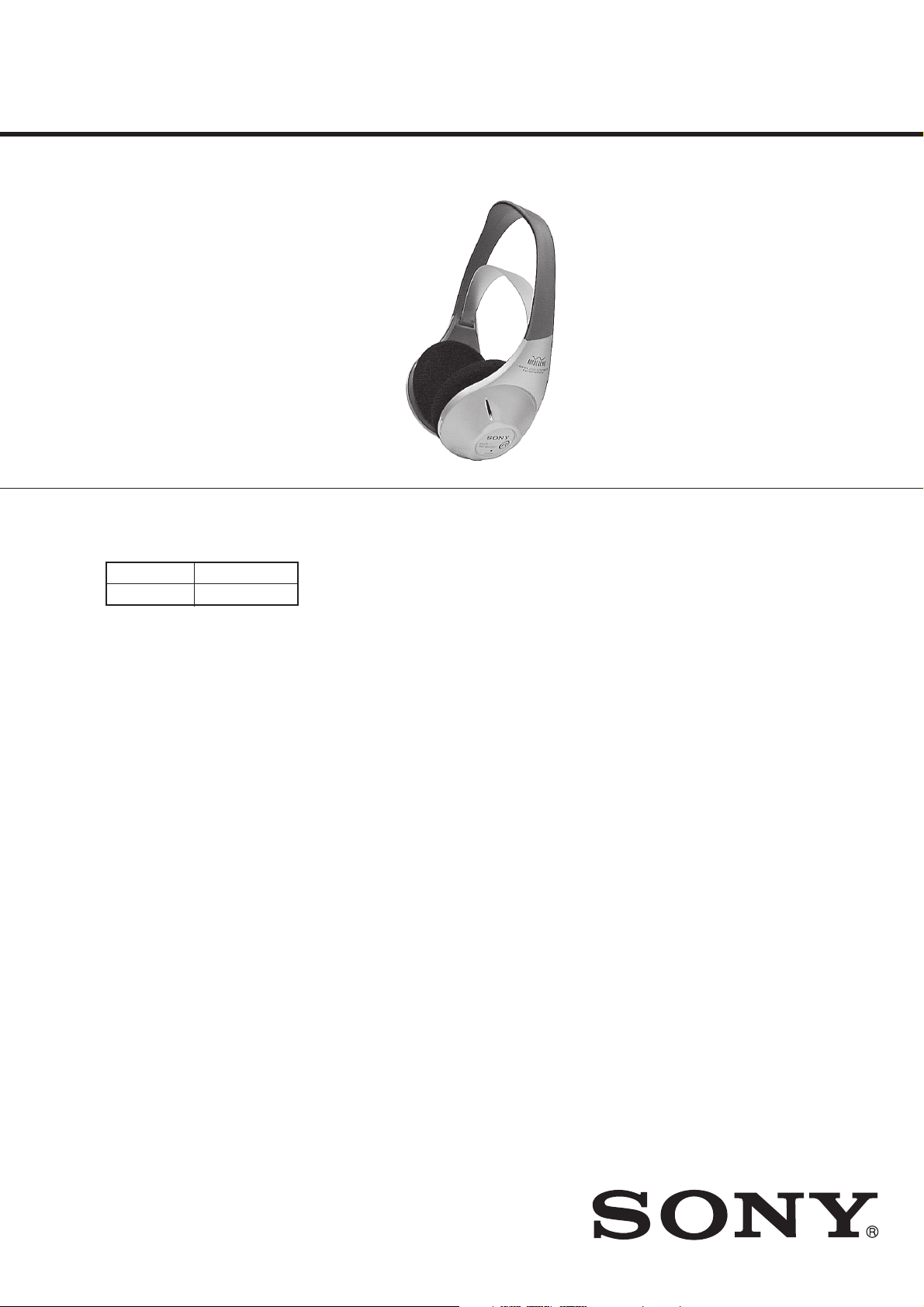
MDR-RF815R
SERVICE MANUAL
Ver 1.2 2001. 11
MDR-RF815R is the component model block one in the MDR-RF815RK.
COMPONENT MODEL NAME FOR MDR-RF815RK
Headphones MDR-RF815R
Transmitter TMR-RF815R
AEP Model
UK Model
SPECIFICATIONS
Headphones
Power source DC 2.4 V: Built-in rechargeable
Mass Approx. 240 g (8.1 oz.) incl.
built-in rechargeable battery
Built-in Ni-Cd rechargeable battery
Model name NC-AA
Voltage 1.2 V
Capacity 700 mAh
Design and specifications are subject to change without
notice.
battery
9-927-956-12
2001K1600-1
© 2001.11
HEADPHONES
Sony Corporation
Personal Audio Company
Published by Sony Engineering Corporation
Page 2

5
-B Turn up the volume to a moderate
level with the VOL control, then
tune the headphones in to the
frequency of the transmitter with the
TUNING control until you can hear
the audio signal loud and clear.
B MDR-RF815R
TUNING
control
VOL control
SECTION 1
GENERAL
Auto power on/off function
When you remove the headphones from your
head, the power turns off automatically. Do not
allow the self adjusting band to be pulled up,
otherwise the headphones will be switched on.
This section is extracted
from instruction manual.
The power turns on.
SAFETY CHECK-OUT
After correcting the original service problem, perform the following
safety checks before releasing the set to the customer.
1. Check the area of your repair for unsoldered or poorly-soldered
connections. Check the entire board surface for solder splashes
and bridges.
2. Check the interboard wiring to ensure that no wires are
"pinched" or contact high-wattage resistors.
3. Look for unauthorized replacement parts, particularly
transistors, that were installed during a previous repair . Point
them out to the customer and recommend their replacement.
4. Look for parts which, through functioning, show obvious signs
of deterioration. Point them out to the customer and
recommend their replacement.
5. Check the B+ voltage to see it is at the values specified.
6. Flexible Circuit Board Repairing
• Keep the temperature of the soldering iron around 270˚C
during repairing.
• Do not touch the soldering iron on the same conductor of the
circuit board (within 3 times).
• Be careful not to apply force on the conductor when soldering
— 2 —
Page 3

SECTION 2
DISASSEMBLY
Note : Follow the disassembly procedure in the numerical order given.
2-1. RX-BASE BOARD
1
Four screws (P 2
× 6)
Cover (R), hanger
Claw
Precaution for installtion
1
Slide the suspender in the
direction of the arrow.
Suspender
2
Set the psuh
switch (1 key).
7
9
Switch, push (1 key)
8
Remove the two solderings.
6
5
2
Claw
RX-BASE board
4
Screw (P 2
3
Remove the
nine solderings.
× 8)
Precaution for installtion
No.205
RX-BASE board
No.204
No.201
No.201 (green)
No.202
No.203
No.203 (black)
Solder the each lead wires directly to the position as shown
while being cautions of colors.
No.204
No.202 (red)
— 3 —
Page 4

Set the lead wires
Set the each lead wires as illustrated below.
B
Cover (L), hanger
Groove
No.203
No.201
To the driver (030F032//K).
Groove
No.201, No.203
Groove
Groove
No.202
Groove
To the RX-BASE board
A
Cover (R), hanger
No.205
Groove
No.204
To the driver (030F032//K).
No.201
No.203
No.202
No.201, No.203
B
Cover (L), hanger
Groove
Cover (R), hanger
A
— 4 —
Page 5

SECTION 3
ELECTRICAL ADJUSTMENTS
Ver 1.2 2001. 11
Notes:
1. Use transmitter with check and adjustment already completed.
2. On adjusting the headphones section, use the transmitter as a
jig.
Headphones:MDR-RF815R
Transmitter:TMR-RF815R
Procedure:
1. Connect an oscillator with attenuator and terminator (600 Ω)
to the transmitter AUDIO IN-A connector (J402).
2. Connect an AC adapter to the transmitter DC IN 9V jack (J404).
3. Connect lead wires to IC301 pin 4, pin 6, pin 7 and GND on
the RX-BASE board.
4. Connect a resistor 33k Ω between IC301 pin 4 and pin 7.
5. Connect lead wires to the speakers’ terminals (L+,L-,R+,R-)
on the RX-BASE board.
3-1. Free run frequency check and adjustment
1. Set the transmitter AUDIO IN-A connector (J402) to no signal.
Note: In this case, operation time is about 4 or 5 minutes.
2. Check the transmitter power indicator (red) lights.
3. Set the transmitter CHANNEL switch to 1.
4. Set the head phones tuning (RV303) to center position.
5. Connect a frequency counter to IC301 pin 4 and GND on the
RX board.
6. Adjust the value of the frequency counter to specification by
RV301 on the RX-BASE board.
Specified Values: 76kHz ± 50Hz.
7. Remove the resistor 33k Ω between IC301 pin 4 and pin 7.
3-2. Receive frequency check and adjustment
1. Set the transmitter CHANNEL switch to 2.
2. Set the transmitter NOISE FILTER switch to OFF.
3. Input a signal of 1kHz, 316mVrms to transmitter AUDIO INA-L connector only.
4. Keep distance transmitter and headphones to 5 meter over.
5. Set the headphones volume (RV302) to minimum.
6. Set the headphones tuning (RV303) to center position.
7.
Connect an oscilloscope CH1 and CH2 to IC301 pin 6 and pin 4.
8. Check the waveform of the oscilloscope to CH1 is demodulated
1kHz signal and CH2 is GND.
9. If CH1 and CH2 are not satisfied step 8, adjust the coil (L301)
on the RX board to satisfied step 8.
10. Set the transmitter CHANNEL switch to 1 or 3.
11. Adjust the headphones tuning (RV303) to receive radio
frequency.
12. Check same step 8.
3-3. Carrier modulation check
1. Set the transmitter CHANNEL switch to 2.
2. Set the transmitter NOISE FILTER switch to OFF.
3. Input a signal of 1kHz, 316mVrms to transmitter AUDIO INA-L connector only.
4. Adjust the headphones tuning (RV303) to receive radio
freqency.
5. Set the headphones volume (RV302) to minimum.
6.
Connect an oscilloscope CH1 and CH2 to IC301 pin 6 and pin 4.
7. Check the waveform of the oscilloscope to CH1 is demodulated
1kHz signal and CH2 is GND.
8. Connect an AC volt meter to IC301 pin 6 and GND.
9. Check the value of the AC volt meter to 26mVrms ± 2mV
3-4. Separation check
1. Set the transmitter CHANNEL switch to 2.
2. Set the transmitter NOISE FILTER switch to OFF.
3. Input a signal of 1kHz, 316mVrms to transmitter AUDIO INA-L connector only.
4. Adjust the headphones tuning (RV303) to receive radio
freqency.
5. Connect an oscilloscope to CH1 is demodulated 1kHz signal
and CH2 is GND.
6. Check the waveform of the oscilloscope to CH1 is demodulated
1kHz signal and CH2 is GND.
7.
Connect an AC volt meter with LPF to speakers terminal (L+,L-).
8. Adjust the value of the AC volt meter to specification by
headphones volume RV302.
Specified Value: 155mVrms
9.
Connect an AC volt meter with LPF to speakers terminal (R+,R-).
10. Measure the value of the AC volt meter.
11. Check the difference of the L and R to more than 20dB.
12. Input a signal of 1kHz, 316mVrms to transmitter AUDIO INA-R connector only.
13. Connect an AC volt meter to speakers terminal (R+,R-).
14. Adjust the value of the AC volt meter to specification by
headphones volume RV302.
Specified Value: 155mVrms
15. Connect an AC volt meter to speakers terminal (L+,L-).
16. Measure the value of the AC volt meter.
17. Check the difference of the L and R to more than 20dB.
Adjustment Location : (See page 6)
— 5 —
Page 6

Adjustment Location :
[RX-BASE BOARD]
(Conductor side)
— 6 —
Page 7

4-1. BLOCK DIAGRAM
FRONT END
FE UNIT
16
D301
18
RECEIVE
FM FE
+V
L301
FREQ.
TUNING
20
22
RV303
+V
L302
CF301
10.7MHz
CF302
10.7MHz
REG
21
+V
SECTION 4
DIAGRAMS
FM IF/
1316
DISCRI
26
AUTO
BLEND
MUTE
IF AMP/DECODE
IC301
PD1
COUNTER
PD1
FREE RUN
1/2
VCO
27
RV301
FREQ.
DECODE
AMP
MONO/ST
SW
STEREO
IND
RV302
VOLUME
B+
POWER
POWER AMP
IC302
ON/OFF SW
D304
S1
Ni-Cd
1.2 x 2
6 2 9
R-CH
5
R-CH
¥
Signal path.
F: FM
SPEAKER
L-CH
SPEAKER
R-CH
+
-
MDR-RF815R
Note on Printed Wiring Board:
• X : parts extracted from the component side.
a
•
• b : Pattern from the side which enables seeing.
Caution:
Pattern face side: Parts on the pattern face side seen from
(SideB) the pattern face are indicated.
Parts face side: Parts on the parts face side seen from
(Side A) the parts face are indicated.
Note on Schematic Diagram:
• All capacitors are in µF unless otherwise noted. pF: µµF 50 WV or
• All resistors are in Ω and 1/
•
• A : B+ Line.
• H : adjustment for repair.
• Power voltage is dc 2.4 V and fed with regulated dc power supply
• Voltages are dc with respect to ground under no-signal conditions .
• Voltages are taken with a VOM (Input impedance 10 MΩ).
• Waveforms are taken with a oscilloscope.
• Circled numbers refer to waveforms.
• Signal path.
: Through hole.
less are not indicated except for electrolytics and tantalums.
4
W or less unless otherwise specified.
f
: internal component.
from battery terminal.
Voltage variations may be noted due to normal production tolerances.
Voltage variations may be noted due to normal production tolerances.
F:FM
L: AUDIO
• IC BLOCK DIAGRAM
IC302 LA4533M
POWER
1
P/SW
IN1
PRE GND
IN2
REF
SWITCH
2
3
4
5
BIAS
AMP1
AMP2
MUTE
CIRCIUT
10
MT/SW
OUT1
9
8
POWER GND
7
OUT2
6
VCC
— 7 — — 8 —
Page 8

MDR-RF815R
4-2. SCHEMATIC DIAGRAM
FREE RUN
FREQ.
5
0.01
2.2
— 9 — — 10 —
Page 9

4-3. PRINTED WIRING BOARD
MDR-RF815R
• Semiconductor
Location
Ref. No. Location
D301 B-1
D304 B-2
D310 C-2
IC301 A-2
IC302 C-2
RV303
RECHARGEABLE
Ni-cd
NC-AA(HJ)
2pcs,2.4V
RV303
S1
ON/OFF
SWITCH
SPEAKER
(L-ch)
SPEAKER
(R-ch)
— 11 — — 12 —
Page 10

MDR-RF815R
MEMO
Page 11

NOTE:
• -XX, -X mean standardized parts, so they may
have some differences from the original one.
• Items marked “*” are not stocked since they
are seldom required for routine service. Some
delay should be anticipated when ordering these
items.
SECTION 5
EXPLODED VIEWS
• The mechanical parts with no reference number
in the exploded views are not supplied.
• Hardware (# mark) list and accessories and
packing materials are given in the last of this
parts list.
1
Ver 1.1 2000. 11
• Color Indication of Appearance Parts Example:
KNOB, BALANCE (WHITE) . . . (RED)
↑ ↑
Parts of Color Cabinet’s Color
20
23
3
#2
2
b
a
#2
4
5
#1
#1
6
#2
11
7
17
#2
b
a
8
#1
#1
8
#2
9
10
#2
19
24
16
21
1415
9
#1
#2
5
12
13
23
3
4
Ref. No. Part No. Description Remarks Ref. No. Part No. Description Remarks
1 3-046-672-01 SUSPENDER
2 3-046-671-11 BAND,HEAD (BLACK)
2 3-046-671-21 BAND,HEAD (WHITE)
3 3-046-692-01 PAT,EAR
4 1-542-400-11 DRIVER (030F032//K)
5 3-046-685-01 PLATE(L), FRONT
6 3-046-675-11 HANGER (R) (BLACK)
6 3-046-675-21 HANGER (R) (WHITE)
7 1-771-249-11 SWITCH, PUSH (1 KEY)
8 4-992-281-01 HOLDER, BALL SHAFT
9 3-046-673-01 SPRING, FREE ADJUSTMENT
* 10 A-4542-641-A RX-BASE BOARD, COMPLETE
11 3-046-677-11 COVER (R), HANGER (BLACK)
11 3-046-677-21 COVER (R), HANGER (WHITE)
12 3-049-799-01 LIGHT, MDR GUIDE
13 3-046-679-21 CAP(R), ORNAMENTAL (WHITE)
14 3-046-674-01 HANGER (L) (WHITE)
14 3-046-674-11 HANGER (L) (BLACK)
15 3-048-267-01 TERMINAL (MIDWAY), BATTERY
16 3-048-265-01 TERMINAL (+), BATTERY
17 3-048-266-01 TERMINAL (-), BATTERY
19 3-046-676-11 COVER (L), HANGER (BLACK)
19 3-046-676-21 COVER (L), HANGER (WHITE)
20 3-046-678-11 CAP(L), ORNAMENTAL (BLACK)
20 3-046-678-21 CAP(L), ORNAMENTAL (WHITE)
21 3-046-682-01 TERMINAL, CHARGE
23 3-048-264-01 SHEET, ORNAMENTAL CAP ADHESIVE
24 1-756-112-11 BATTERY, NICKEL CADMIUM
#1 7-685-104-19 SCREW +P2X6 TYPE2 NON-SLIT
#2 7-685-105-19 SCREW +P2X8 TYPE2 NON-SLIT
13 3-046-679-11 CAP(R), ORNAMENTAL (BLACK)
— 13 —
Page 12

SECTION 6
RX-BASE
NOTE:
• Due to standardization, replacements in the
parts list may be different from the parts
specified in the diagrams or the components
used on the set.
• -XX, -X mean standardized parts, so they
may have some difference from the original
one.
• Items marked “*” are not stocked since they
are seldom required for routine service.
Some delay should be anticipated when
ordering these items.
Ref. No. Part No. Description Remarks Ref. No. Part No. Description Remarks
* A-4542-641-A RX-BASE BOARD, COMPLETE
************************
* A-4542-642-A RX-FE UNIT (FRONT END)
< CAPACITOR >
C301 1-164-346-11 CERAMIC CHIP 1uF 16V
C302 1-164-005-11 CERAMIC CHIP 0.47uF 25V
C303 1-124-259-11 ELECT 4.7uF 20.00% 16V
C304 1-163-037-11 CERAMIC CHIP 0.022uF 10% 25V
C305 1-163-037-11 CERAMIC CHIP 0.022uF 10% 25V
C306 1-124-234-00 ELECT 22uF 20% 16V
C307 1-163-059-91 CERAMIC CHIP 0.01uF 10.00% 50V
C308 1-124-234-00 ELECT 22uF 20% 16V
C309 1-124-257-11 ELECT 2.2uF 20.00% 50V
C310 1-104-942-11 ELECT 1uF 20.00% 50V
C311 1-124-233-11 ELECT 10uF 20.00% 16V
C312 1-126-162-11 ELECT 3.3uF 20% 50V
C313 1-163-021-91 CERAMIC CHIP 0.01uF 10.00% 50V
C314 1-164-441-11 CERAMIC CHIP 68PF 5.00% 50V
C315 1-163-235-11 CERAMIC CHIP 22PF 5.00% 50V
C316 1-124-233-11 ELECT 10uF 20.00% 16V
C317 1-163-009-11 CERAMIC CHIP 0.001uF 10% 50V
C319 1-163-021-91 CERAMIC CHIP 0.01uF 10.00% 50V
C320 1-163-038-00 CERAMIC CHIP 0.1uF 25V
C324 1-124-635-00 ELECT 220uF 20.00% 6.3V
C325 1-124-635-00 ELECT 220uF 20.00% 6.3V
C326 1-124-635-00 ELECT 220uF 20.00% 6.3V
C327 1-163-038-00 CERAMIC CHIP 0.1uF 25V
C328 1-163-038-00 CERAMIC CHIP 0.1uF 25V
C329 1-163-021-91 CERAMIC CHIP 0.01uF 10.00% 50V
ELECTRICAL PARTS LIST
• CAPACITORS:
uF: µF
• RESISTORS
All resistors are in ohms.
METAL: metal-film resistor
METAL OXIDE: Metal Oxide-film resistor
F: nonflammable
• COILS
uH: µH
C355 1-163-009-11 CERAMIC CHIP 0.001uF 10% 50V
C357 1-163-021-91 CERAMIC CHIP 0.01uF 10.00% 50V
C361 1-163-251-11 CERAMIC CHIP 100PF 5.00% 50V
C362 1-163-251-11 CERAMIC CHIP 100PF 5.00% 50V
C363 1-163-021-91 CERAMIC CHIP 0.01uF 10.00% 50V
C364 1-163-009-11 CERAMIC CHIP 0.001uF 10% 50V
C365 1-163-009-11 CERAMIC CHIP 0.001uF 10% 50V
C366 1-163-009-11 CERAMIC CHIP 0.001uF 10% 50V
CF301 1-577-588-11 FILTER, CERAMIC 10.7MHz
CF302 1-577-572-11 FILTER, CERAMIC 10.7MHz
D301 8-719-002-81 DIODE 1T363
D304 8-719-077-16 LED SLR-342VC3F (power)
D310 8-719-975-40 DIODE RB411D
IC301 8-752-072-12 IC CXA1538N
IC302 8-759-802-75 IC LA4533M
JC301 1-216-295-91 SHORT 0
JC303 1-216-295-91 SHORT 0
JC305 1-216-295-91 SHORT 0
JC309 1-216-295-91 SHORT 0
JC311 1-216-295-91 SHORT 0
JC324 1-216-295-91 SHORT 0
• SEMICONDUCTORS
In each case, u: µ, for example:
uA...: µA... , uPA... , µPA... ,
uPB... , µPB... , uPC... , µPC... ,
uPD..., µPD...
When indicating parts by reference number,
please include the board name.
< FILTER >
< DIODE >
< IC >
< JUMPER >
C330 1-124-242-00 ELECT 33uF 20% 25V
C331 1-163-021-11 CERAMIC CHIP 0.01uF 10% 50V
C332 1-163-245-11 CERAMIC CHIP 56PF 5.00% 50V
C333 1-163-222-11 CERAMIC CHIP 5PF 0.25PF 50V
C334 1-164-346-11 CERAMIC CHIP 1uF 16V
C336 1-163-245-11 CERAMIC CHIP 56PF 5.00% 50V
C345 1-163-021-11 CERAMIC CHIP 0.1uF 25V
C350 1-164-346-11 CERAMIC CHIP 1uF 16V
C351 1-164-346-11 CERAMIC CHIP 1uF 16V
C352 1-163-009-11 CERAMIC CHIP 0.001uF 10% 50V
< COIL >
L301 1-422-317-31 COIL, AIR-CORE
L302 1-412-933-11 INDUCTOR 0.33uH
L304 1-414-234-11 INDUCTOR CHIP 0uH
L305 1-414-234-11 INDUCTOR CHIP 0uH
L306 1-414-234-11 INDUCTOR CHIP 0uH
L307 1-414-234-11 INDUCTOR CHIP 0uH
L308 1-414-766-21 INDUCTOR CHIP 0uH
L309 1-414-766-21 INDUCTOR CHIP 0uH
Page 13

RX-BASE
Ref. No. Part No. Description Remarks Ref. No. Part No. Description Remarks
< RESISTOR >
R302 1-216-057-00 METAL CHIP 2.2K 5% 1/10W
R304 1-216-061-00 METAL CHIP 3.3K 5% 1/10W
R305 1-216-061-00 METAL CHIP 3.3K 5% 1/10W
R308 1-216-057-00 METAL CHIP 2.2K 5% 1/10W
R309 1-216-097-91 RES-CHIP 100K 5% 1/10W
R327 1-216-085-00 METAL CHIP 33K 5% 1/10W
R328 1-216-085-00 METAL CHIP 33K 5% 1/10W
R330 1-216-001-00 METAL CHIP 10 5% 1/10W
R333 1-216-057-00 METAL CHIP 2.2K 5% 1/10W
R334 1-216-057-00 METAL CHIP 2.2K 5% 1/10W
< VARIABLE RESISTOR >
R310 1-216-061-00 METAL CHIP 3.3K 5% 1/10W
R312 1-216-077-00 RES-CHIP 15K 5% 1/10W
R314 1-216-097-91 RES-CHIP 100K 5% 1/10W
R315 1-216-001-00 METAL CHIP 10 5% 1/10W
R316 1-216-001-00 METAL CHIP 10 5% 1/10W
R320 1-216-001-00 METAL CHIP 10 5% 1/10W
R321 1-216-053-00 METAL CHIP 1.5K 5% 1/10W
R322 1-216-069-00 METAL CHIP 6.8K 5% 1/10W
R323 1-216-069-00 METAL CHIP 6.8K 5% 1/10W
R325 1-216-037-00 METAL CHIP 330 5% 1/10W
RV301 1-241-763-11 RES, ADJ, CARBON 4.7K
RV302 1-227-189-11 RES, VAR CARBON 20K/20K (VOLUME)
RV303 1-227-190-11 RES, VAR CARBON 10K (TUNING)
**************************************************************
MISCELLANEOUS
**************
4 1-542-400-11 DRAIVER (030F032//K)
7 1-771-249-11 SWITCH, PUSH (1 KEY)
**************************************************************
— 15 —
Page 14

MDR-RF815R
REVISION HISTORY
Clicking the version allows you to jump to the revised page.
Also, clicking the version at the upper right on the revised page allows you to jump to the next revised
page.
Ver. Date Description of Revision
1.2 2001.11 Correction of electrical adjustments
1.1 2000.11 Change of exploded view
1.0 2000.06 New
(ENG-01023)
(ENG-00019)
 Loading...