

Page 1
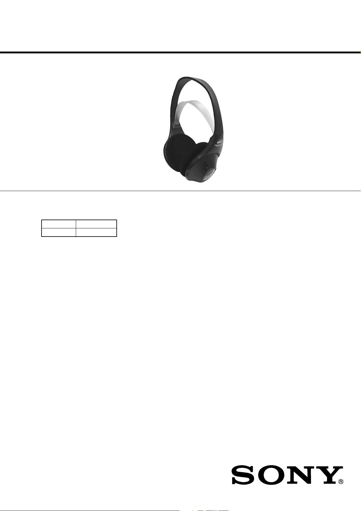
MDR-RF415R
SERVICE MANUAL
Ver 1.0 2001. 02
MDR-RF415R is the component model block one in the MDR-RF415RK.
COMPONENT MODEL NAME FOR MDR-RF415RK
Headphones MDR-RF415R
Transmitter TMR-RF415R
AEP Model
SPECIFICATIONS
Power source DC 2.4 V: Built-in rechargeable battery
Mass Approx. 240 g (8.5 oz.) incl.
built-in rechargeable battery
Built-in Ni-Cd rechargeable battery
Model name NC-AA
V oltage 1.2 V
Capacity 700 mAh
Design and specifications are subject to change without notice.
HEADPHONES
9-873-075-11
2001B1600-1
© 2001.2
Sony Corporation
Audio Entertainment Group
General Engineering Dept.
Page 2
MDR-RF415R
SECTION 1
GENERAL
This section is extracted
from instruction manual.
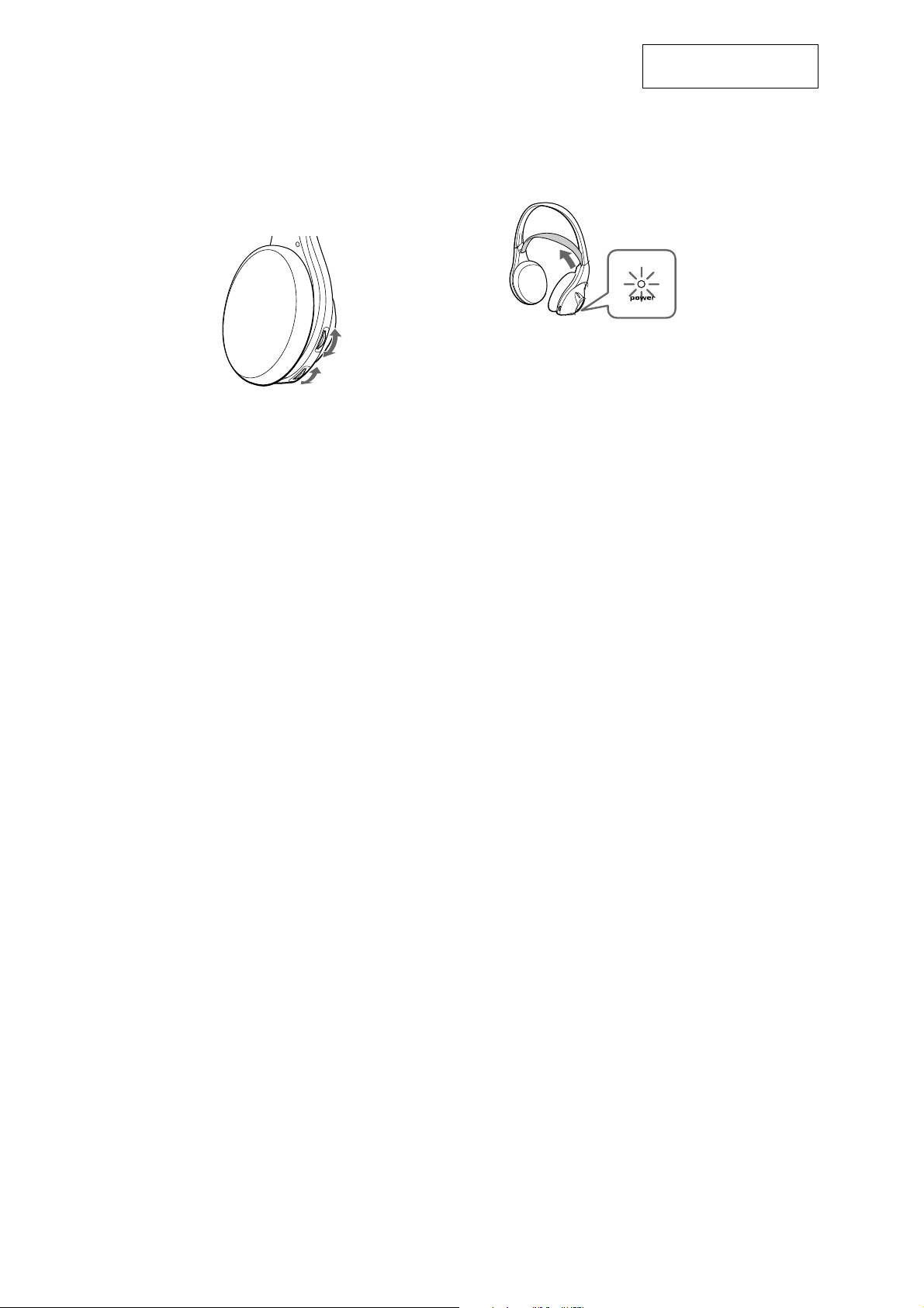
5
Turn up the volume to a moderate level
with the VOL control, then tune the
headphones in to the frequency of the
transmitter with the TUNING control
until you can hear the audio signal
loud and clear.
TUNING
control
VOL control
Auto power on/off function
When you remove the headphones from your
head, the power turns off automatically. Do not
allow the self adjusting band to be pulled up,
otherwise the headphones will be switched on.
The power turns on.
Notes on chip component replacement
• Never reuse a disconnected chip component.
• Notice that the minus side of a tantalum capacitor may be
damaged by heat.
2
Page 3
SECTION 2
DISASSEMBLY
Note : Follow the disassembly procedure in the numerical order given.
2-1. RX-BASE BOARD
1
Five screws (P 2
MDR-RF415R
× 6)
Cover (R), hanger
Claw
Precaution for installtion
1
Slide the suspender in the
direction of the arrow.
Suspender
2
Set the push
switch (1 key).
7
9
Switch, push (1 key)
8
Remove the two solderings.
6
5
2
Claw
RX-BASE board
4
Screw (P 2
3
Remove the
nine solderings.
× 8)
Precaution for installtion
No.205
RX-BASE board
No.204
No.201
No.201 (green)
No.202
No.203
No.203 (black)
Solder the each lead wires directly to the position as shown
while being cautions of colors.
No.204
No.202 (red)
3
Page 4
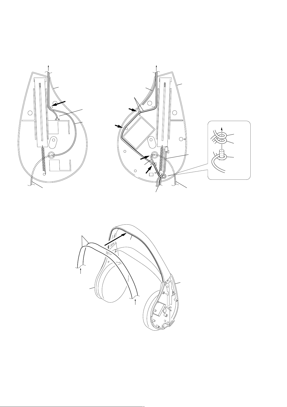
MDR-RF415R
Set the lead wires
Set the each lead wires as illustrated below.
B
Cover (L), hanger
Groove
No.203
No.201
To the driver (030F032//K).
Groove
No.205
No.201, No.203
Groove
Groove
No.202
Groove
To the RX-BASE board
A
Cover (R), hanger
No.204
To the driver (030F032//K).
No.203
No.201
No.202
No.201, No.203
B
Cover (L), hanger
Groove
Cover (R), hanger
A
4
Page 5

SECTION 3
ELECTRICAL ADJUSTMENTS
MDR-RF415R
Notes:
1. Use transmitter with check and adjustment already completed.
2. On adjusting the headphones section, use the transmitter as a
jig.
Headphones:MDR-RF415R
Transmitter:TMR-RF415R
Procedure:
1. Connect an oscillator with attenuator and terminator (600 Ω)
to the transmitter AUDIO IN-A connector (J402).
2. Connect an A C adapter to the transmitter DC IN 9V jack (J404).
3. Connect lead wires to IC301 pin 4, pin 6, pin 7 and GND on
the RX-BASE board.
4. Connect a resistor 33k Ω between IC301 pin 4 and pin 7.
5. Connect lead wires to the speakers’ terminals (L+,L-,R+,R-)
on the RX-BASE board.
3-1. Free run frequency check and adjustment
1. Set the transmitter A UDIO IN-A connector (J402) to no signal.
Note: In this case, operation time is about 4 or 5 minutes.
2. Check the transmitter power indicator (red) lights.
3. Set the transmitter CHANNEL switch to 1.
4. Set the headphones tuning (RV303) to center position.
5. Connect a frequency counter to IC301 pin 4 and GND on the
RX-BASE board.
6. Adjust the value of the frequency counter to specification by
RV301 on the RX-BASE board.
Specified Values: 76kHz ± 50Hz.
3-2. Receive frequency check and adjustment
1. Set the transmitter CHANNEL switch to 2.
2. Set the transmitter NOISE FILTER switch to OFF.
3. Input a signal of 1kHz, 316mVrms to transmitter
AUDIO IN-A-L connector only.
4. Keep distance transmitter and headphones to 5 meters over.
5. Set the headphones volume (RV302) to minimum.
6. Set the headphones tuning (RV303) to center position.
Connect an oscilloscope CH1 and CH2 to IC301 pin 6 and pin 4.
7.
8. Check the waveform of the oscilloscope to CH1 is demodulated
1kHz signal and CH2 is GND.
9. If CH1 and CH2 are not satisfied step 8, adjust the coil (L301)
on the RX-BASE board to satisfied step 8.
10. Set the transmitter CHANNEL switch to 1 or 3.
11. Adjust the headphones tuning (RV303) to receive radio
frequency.
12. Check same step 8.
3-3. Carrier modulation check
1. Set the transmitter CHANNEL switch to 2.
2. Set the transmitter NOISE FILTER switch to OFF.
3. Input a signal of 1kHz, 316mVrms to transmitter
AUDIO IN-A-L connector only.
4. Adjust the headphones tuning (RV303) to receive radio
freqency.
5. Set the headphones volume (RV302) to minimum.
6.
Connect an oscilloscope CH1 and CH2 to IC301 pin 6 and pin 4.
7. Check the waveform of the oscilloscope to CH1 is demodulated
1kHz signal and CH2 is GND.
8. Connect an AC volt meter to IC301 pin 6 and GND.
9. Check the value of the AC volt meter to 26mVrms ± 2mV
3-4. Separation check
1. Set the transmitter CHANNEL switch to 2.
2. Set the transmitter NOISE FILTER switch to OFF.
3. Input a signal of 1kHz, 316mVrms to transmitter
AUDIO IN-A-L connector only.
4. Adjust the headphones tuning (RV303) to receive radio
freqency.
5. Connect an oscilloscope to CH1 is demodulated 1kHz signal
and CH2 is GND.
6. Check the waveform of the oscilloscope to CH1 is demodulated
1kHz signal and CH2 is GND.
7.
Connect an A C v olt meter with LPF to speakers terminal (L+,L-).
8. Adjust the value of the AC volt meter to specification by
headphones volume (RV302).
Specified V alue: 155mVrms
9.
Connect an A C volt meter with LPF to speak ers terminal (R+,R-).
10. Measure the value of the AC volt meter.
11. Check the difference of the L and R to more than 20dB.
12. Input a signal of 1kHz, 316mVrms to transmitter
AUDIO IN-A-R connector only.
13. Connect an AC volt meter to speakers terminal (R+,R-).
14. Adjust the value of the AC volt meter to specification by
headphones volume (RV302).
Specified V alue: 155mVrms
15. Connect an AC volt meter to speakers terminal (L+,L-).
16. Measure the value of the AC volt meter.
17. Check the difference of the L and R to more than 20dB.
Adjustment Location : (See page 6)
5
Page 6
MDR-RF415R
Adjustment Location :
[RX-BASE BOARD]
(Conductor side)
IC301
7
IC301
4
IC301
6
GND
RV303
R323
C334
JC324
power
L–
L+
R–
R+
6
Page 7
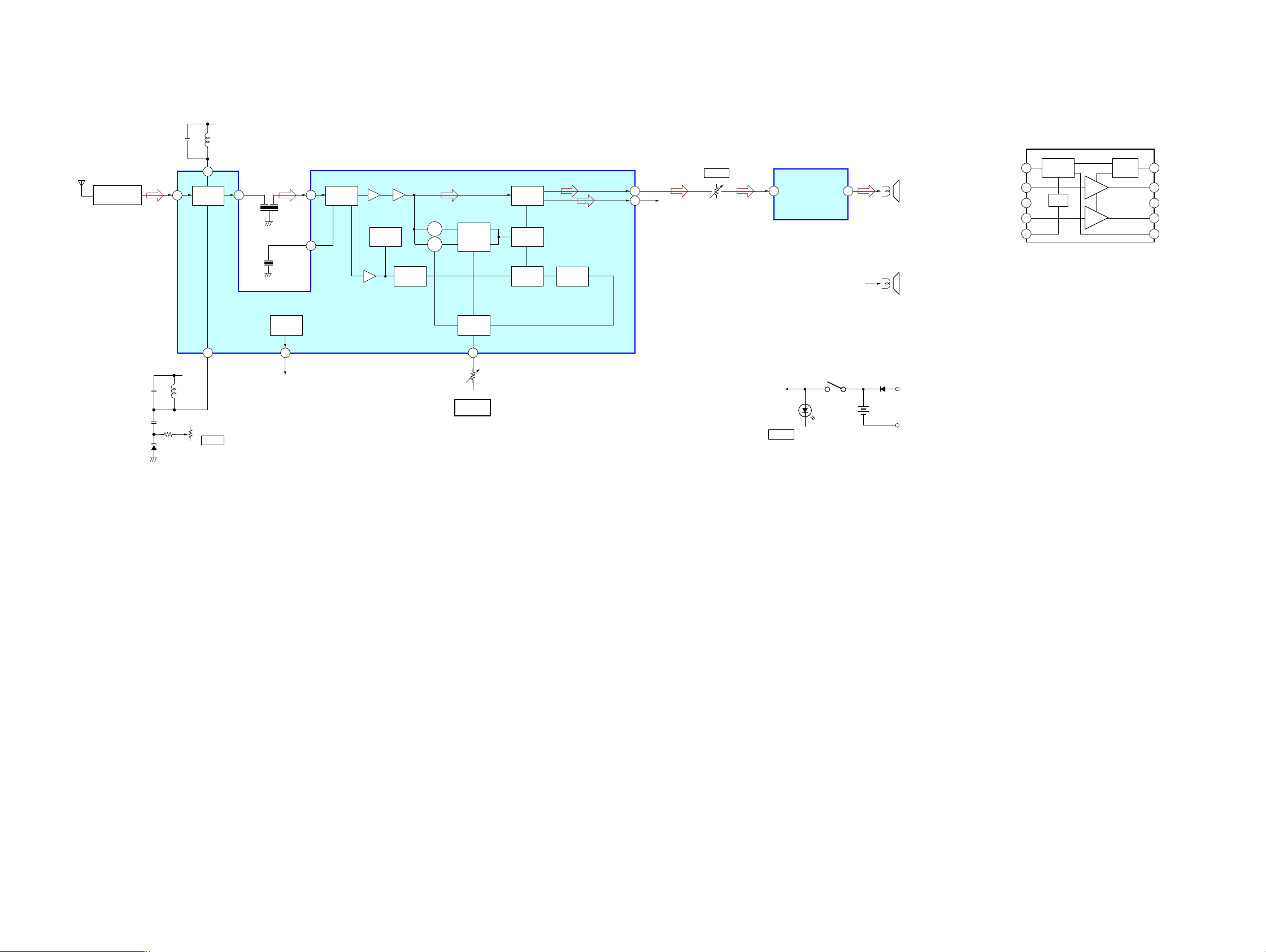
SECTION 4
DIAGRAMS
MDR-RF415R
4-1. BLOCK DIAGRAM
FRONT END
FE UNIT
D301
18
RECEIVE
+V
L301
FREQ.
20
FM FE
22
RV303
TUNE
+V
L302
CF301
10.7MHz
CF302
10.7MHz
REG
21
+V
• IC BLOCK DIAGRAM
IC302 LA4533M
IF AMP/DECODE
IC301
FM IF/
1316
DISCRI
MUTE
PD1
PD1
1/2
COUNTER
VCO
27
RV301
FREE RUN
FREQ.
AUTO
26
BLEND
DECODE
AMP
MONO/ST
SW
STEREO
IND
6 2 9
R-CH
5
RV302
VOLw
B+
power
AUDIO AMP
IC302
D304
S1
ON/OFF SW
Ni-Cd
1.2 x 2
R-CH
R-ch is omitted.
• Signal path.
F: FM
SPEAKER
L-CH
SPEAKER
R-CH
+
-
P/SW
IN1
PRE GND
IN2
REF
AMP1
AMP2
MUTE
CIRCIUT
10
MT/SW
OUT1
9
8
POWER GND
7
OUT2
6
VCC
POWER
1
SWITCH
2
BIAS
3
4
5
77
Page 8

MDR-RF415R
4-2. SCHEMATIC DIAGRAM
HVU363ATRU
FREE RUN
FREQ.
TUNE
5
IC B/D
TO
VOLw
C345
0.01
2.2
0.01
B
TLSU124
TMR-RF415R
Note on Schematic Diagram:
• All capacitors are in µF unless otherwise noted. pF: µµF 50 WV or
less are not indicated except for electrolytics and tantalums.
• All resistors are in Ω and 1/
• A : B+ Line.
4
W or less unless otherwise specified.
• H : adjustment for repair.
• Power voltage is dc 2.4 V and fed with regulated dc power supply
from battery terminal.
• Voltages are dc with respect to ground under no-signal conditions.
• Voltages are taken with a VOM (Input impedance 10 MΩ).
Voltage variations may be noted due to normal production tolerances.
• Signal path.
F:FM
88
Page 9

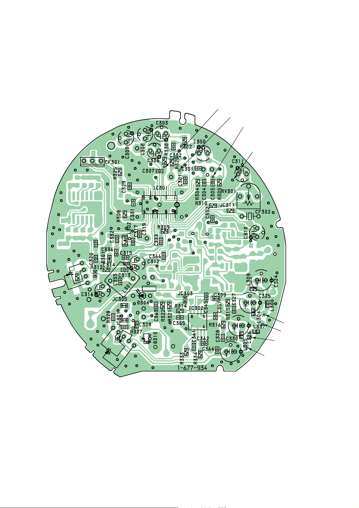
4-3. PRINTED WIRING BOARD
MDR-RF415R
• Semiconductor
Location
Ref. No. Location
D301 B-1
D304 B-2
D310 C-2
IC301 A-2
IC302 C-2
IC301
RV303
TUNE
RECHARGEABLE
Ni-cd
NC-AA(HJ)
2pcs,2.4V
RV303
R323
VOLw
C334
JC324
power
IC302
TO TMR-RF415R (BATTERY CHARGER)
S1
ON/OFF
SWITCH
SPEAKER
(L-ch)
SPEAKER
(R-ch)
Note on Printed Wiring Board:
• X : parts extracted from the component side.
a
•
• : Pattern from the side which enables seeing.
Caution:
Pattern face side: Parts on the pattern face side seen from
(SideB) the pattern face are indicated.
Parts face side: Parts on the parts face side seen from
(Side A) the parts face are indicated.
: Through hole.
99
Page 10

MDR-RF415R
SECTION 5
EXPLODED VIEWS
RX-BASE
SECTION 6
ELECTRICAL PARTS LIST
NOTE:
• -XX, -X mean standardized parts, so they may
have some differences from the original one.
• Items marked “*” are not stocked since they
are seldom required for routine service. Some
delay should be anticipated when ordering these
items.
• The mechanical parts with no reference number
in the exploded views are not supplied.
• Hardware (# mark) list and accessories and
packing materials are given in the last of this
parts list.
1
3
#3
2
b
a
#2
4
5
#1
#1
6
#3
23
20
19
#2
#1
b
a
8
#1
#1
8
#2
S1
10
#3
7
9
11
17
16
12
21
1415
#1
#2
9
18
Ref. No. Part No. Description Remarks Ref. No. Part No. Description Remarks
1 3-046-672-01 SUSPENDER
2 3-046-671-11 BAND, HEAD
3 3-046-692-01 PAT, EAR
4 1-542-400-11 DRIVER (030F032//K)
5 3-046-685-01 PLATE (L), FRONT
6 3-046-675-31 HANGER (R)
7 3-846-312-01 SPACER
8 4-992-281-01 HOLDER, BALL SHAFT
9 4-981-975-01 SPRING, TENSION
* 10 A-4542-692-A RX-BASE BOARD, COMPLETE
5
4
14 3-046-674-11 HANGER (L)
15 3-048-267-01 TERMINAL (MIDWAY), BATTERY
16 3-048-265-01 TERMINAL (+), BATTERY
17 3-048-266-01 TERMINAL (-), BATTERY
18 1-756-112-11 BATTERY, NICKEL CADMIUM
19 3-046-676-11 COVER (L), HANGER
20 3-046-678-31 CAP (L), ORNAMENTAL
21 3-046-682-01 TERMINAL, CHARGE
23 3-048-264-01 SHEET, ORNAMENTAL CAP ADHESIVE
S1 1-771-249-11 SWITCH, PUSH (1 KEY) (ON/OFF)
23
13
3
NOTE:
• Due to standardization, replacements in the
parts list may be different from the parts
specified in the diagrams or the components
used on the set.
• -XX, -X mean standardized parts, so they
may have some difference from the original
one.
• Items marked “*” are not stocked since they
are seldom required for routine service.
Some delay should be anticipated when
ordering these items.
Ref. No. Part No. Description Remarks Ref. No. Part No. Description Remarks
* A-4542-692-A RX-BASE MOUNTED BOARD, COMPLETE
*********************************
3-046-682-01 TERMINAL, CHARGE
< CAPACITOR >
C301 1-164-346-11 CERAMIC CHIP 1uF 16V
C302 1-164-005-11 CERAMIC CHIP 0.47uF 25V
C303 1-124-259-11 ELECT 4.7uF 20.00% 16V
C304 1-163-037-11 CERAMIC CHIP 0.022uF 10% 25V
C305 1-163-037-11 CERAMIC CHIP 0.022uF 10% 25V
C306 1-124-234-00 ELECT 22uF 20% 16V
C307 1-163-059-00 CERAMIC CHIP 0.01uF 10.00% 50V
C308 1-124-234-00 ELECT 22uF 20% 16V
C309 1-124-257-00 ELECT 2.2uF 20% 50V
C310 1-104-942-11 ELECT 1uF 20.00% 50V
C311 1-124-233-11 ELECT 10uF 20.00% 16V
C312 1-126-162-11 ELECT 3.3uF 20% 50V
C313 1-163-021-11 CERAMIC CHIP 0.01uF 10.00% 50V
C314 1-164-441-11 CERAMIC CHIP 68PF 5.00% 50V
C315 1-163-235-11 CERAMIC CHIP 22PF 5.00% 50V
C316 1-124-233-11 ELECT 10uF 20.00% 16V
C317 1-163-009-11 CERAMIC CHIP 0.001uF 10% 50V
C319 1-163-021-11 CERAMIC CHIP 0.01uF 10.00% 50V
C320 1-163-038-11 CERAMIC CHIP 0.1uF 25V
C324 1-124-635-00 ELECT 220uF 20.00% 6.3V
C325 1-124-635-00 ELECT 220uF 20.00% 6.3V
C326 1-124-635-00 ELECT 220uF 20.00% 6.3V
C327 1-163-038-11 CERAMIC CHIP 0.1uF 25V
C328 1-163-038-11 CERAMIC CHIP 0.1uF 25V
C329 1-163-021-11 CERAMIC CHIP 0.01uF 10.00% 50V
C330 1-124-242-00 ELECT 33uF 20% 25V
C331 1-163-021-11 CERAMIC CHIP 0.01uF 10.00% 50V
C332 1-163-245-11 CERAMIC CHIP 56PF 5.00% 50V
C333 1-163-222-11 CERAMIC CHIP 5PF 0.25PF 50V
C334 1-164-346-11 CERAMIC CHIP 1uF 16V
C336 1-163-245-11 CERAMIC CHIP 56PF 5.00% 50V
C345 1-163-021-11 CERAMIC CHIP 0.01uF 10.00% 50V
C350 1-164-346-11 CERAMIC CHIP 1uF 16V
C351 1-164-346-11 CERAMIC CHIP 1uF 16V
C352 1-163-009-11 CERAMIC CHIP 0.001uF 10% 50V
• CAPACITORS:
uF: µF
• RESISTORS
All resistors are in ohms.
METAL: metal-film resistor
METAL OXIDE: Metal Oxide-film resistor
F: nonflammable
• COILS
uH: µH
C355 1-163-009-11 CERAMIC CHIP 0.001uF 10% 50V
C357 1-163-021-11 CERAMIC CHIP 0.01uF 10.00% 50V
C361 1-163-251-11 CERAMIC CHIP 100PF 5.00% 50V
C362 1-163-251-11 CERAMIC CHIP 100PF 5.00% 50V
C363 1-163-021-11 CERAMIC CHIP 0.01uF 10.00% 50V
C364 1-163-009-11 CERAMIC CHIP 0.001uF 10% 50V
C365 1-163-009-11 CERAMIC CHIP 0.001uF 10% 50V
C366 1-163-009-11 CERAMIC CHIP 0.001uF 10% 50V
CF301 1-577-588-11 FILTER, CERAMIC
CF302 1-577-572-11 FILTER, CERAMIC
D301 8-719-083-90 DIODE HVU363ATRU
D304 8-719-077-16 DIODE TLSU124 (TPJ52) (power)
D310 8-719-975-40 DIODE RB411D
IC301 8-752-072-12 IC CXA1538N-T4
IC302 8-759-802-75 IC LA4533MTP-1
JC301 1-216-295-11 SHORT 0
JC303 1-216-295-11 SHORT 0
JC305 1-216-295-11 SHORT 0
JC309 1-216-295-11 SHORT 0
JC311 1-216-295-11 SHORT 0
JC324 1-216-295-11 SHORT 0
L301 1-422-317-31 COIL, AIR-CORE
L302 1-412-933-11 INDUCTOR 0.33uH
L304 1-414-234-11 FERRITE 0uH
L305 1-414-234-11 FERRITE 0uH
L306 1-414-234-11 FERRITE 0uH
L307 1-414-234-11 FERRITE 0uH
L308 1-414-234-11 FERRITE 0uH
L309 1-414-234-11 FERRITE 0uH
• SEMICONDUCTORS
In each case, u: µ, for example:
uA...: µA... , uPA... , µPA... ,
uPB... , µPB... , uPC... , µPC... ,
uPD..., µPD...
When indicating parts by reference number,
please include the board name.
< FILTER >
< DIODE >
< IC >
< JUMPER >
< COIL >
11 3-046-677-11 COVER (R), HANGER
12 3-049-799-01 LIGHT, MDR GUIDE
13 3-046-679-31 CAP (R), ORNAMENTAL
#1 7-685-104-19 SCREW +P 2X6 TYPE2 NON-SLIT
#2 7-685-105-19 SCREW +P 2X8 TYPE2 NON-SLIT
#3 3-223-909-01 SCREW (B2)
1010
Page 11

MDR-RF415R
RX-BASE
Ref. No. Part No. Description Remarks Ref. No. Part No. Description Remarks
< RESISTOR >
R302 1-216-057-00 METAL CHIP 2.2K 5% 1/10W
R304 1-216-061-00 METAL CHIP 3.3K 5% 1/10W
R305 1-216-061-00 METAL CHIP 3.3K 5% 1/10W
R308 1-216-057-00 METAL CHIP 2.2K 5% 1/10W
R309 1-216-097-11 RES-CHIP 100K 5% 1/10W
R327 1-216-085-00 METAL CHIP 33K 5% 1/10W
R328 1-216-085-00 METAL CHIP 33K 5% 1/10W
R330 1-216-001-00 METAL CHIP 10 5% 1/10W
R333 1-216-057-00 METAL CHIP 2.2K 5% 1/10W
R334 1-216-057-00 METAL CHIP 2.2K 5% 1/10W
< VARIABLE RESISTOR >
R310 1-216-061-00 METAL CHIP 3.3K 5% 1/10W
R312 1-216-077-00 RES-CHIP 15K 5% 1/10W
R314 1-216-097-11 RES-CHIP 100K 5% 1/10W
R315 1-216-001-00 METAL CHIP 10 5% 1/10W
R316 1-216-001-00 METAL CHIP 10 5% 1/10W
R320 1-216-001-00 METAL CHIP 10 5% 1/10W
R321 1-216-053-00 METAL CHIP 1.5K 5% 1/10W
R322 1-216-069-00 METAL CHIP 6.8K 5% 1/10W
R323 1-216-069-00 METAL CHIP 6.8K 5% 1/10W
R325 1-216-037-00 METAL CHIP 330 5% 1/10W
RV301 1-241-763-11 RES, ADJ, CARBON 4.7K
RV302 1-227-189-11 RES, VAR CARBON 20K/20K (VOLw)
RV303 1-227-190-11 RES, VAR CARBON 10K (TUNE)
************************************************************
MISCELLANEOUS
**************
4 1-542-400-11 DRIVER (030F032//K)
18 1-756-112-11 BATTERY, NICKEL CADMIUM
S1 1-771-249-11 SWITCH, PUSH (1 KEY) (ON/OFF)
11
Page 12

MDR0-RF415R
REVISION HISTORY
Clicking the version allows you to jump to the revised page.
Also, clicking the version at the upper right on the revised page allows you to jump to the next revised
page.
Ver. Date Description of Revision
1.0 2001.02 New
Page 13

TMR-RF415R
SERVICE MANUAL
Ver 1.0 2001. 02
TMR-RF415R is the component model block one in the MDR-RF415RK.
COMPONENT MODEL NAME FOR MDR-RF415RK
Headphones MDR-RF415R
Transmitter TMR-RF415R
AEP Model
SPECIFICATIONS
Power source DC 9 V: supplied AC power adaptor
Audio input phono jacks/stereo mini jack
Dimensions Approx. 150 mm dia × 108 mm
Mass Approx. 190 g (6.7 oz.)
Design and specifications are subject to change without notice.
(6 × 4 1/3 in.) (w/h)
9-873-073-11
2001B1600-1
© 2001.2
TRANSMITTER
Sony Corporation
Audio Entertainment Group
General Engineering Dept.
Page 14

TMR-RF415R
Setting up the
SECTION 1
GENERAL
A To connect to a headphones jack
This section is extracted
from instruction manual.
transmitter
1
Connect the transmitter to audio/video
equipment. Select one of the hookups
below depending on the jack type:
Transmitter
OFF ON
FILTERNOISE
Right channel
(red)
Connecting cord
(supplied)
Unimatch plug
adaptor
(supplied)
to headphones
jack (stereo
phone jack)
RBAL
AUDIO IN
CD Walkman,
MD Walkman,
WALKMAN*,
VCR, etc.
to AUDIO IN
A jacks
DC IN 9V
123
CHANNEL
Left channel
(white)
to headphones
jack (stereo
mini jack)
Notes on chip component replacement
• Never reuse a disconnected chip component.
• Notice that the minus side of a tantalum capacitor may be
damaged by heat.
2
Page 15

SECTION 2
)
r
DISASSEMBLY
Note : Follow the disassembly procedure in the numerical order given.
2-1. CABINET (UPPER)
TMR-RF415R
2
Cabinet (upper)
1
Four screws (P 2
× 8
2-2. TX-BASE BOARD
2
TX-BASE board
Cabinet assy, lowe
1
3
Page 16

TMR-RF415R
SECTION 3
ELECTRICAL ADJUSTMENTS
Setting :
AF signal
generator
set
TMR-RF415R
L-CH (J402)
Telescopic
antenna
Frequency counter
8 cm
set
TMR-RF415R
Send Frequency Check
1. Set the NOISE FILTER switch to OFF.
2. Input a signal of 1 kHz 40 mVrms to only the L-CH (J402).
3. Connect a telescopic antenna to the frequency counter input
and extend the antenna to a length of approximately 8 cm.
4. Place TX-BASE board close to the frequenc y counter, then mea-
sure the frequencies of CH1 , CH2 and CH3 and make sure
the values are as follows:
CH1 : 433.5 MHz ± 40 kHz
CH2 : 434.0 MHz ± 40 kHz
CH3 : 434.5 MHz ± 40 kHz
Pilot signal Modulation Check and Adjustment
1. Set the channel to CH2 .
2. No signal input (The operating time in this case is limited to 4
or 5 minutes.)
3. Measure the movable terminal of RV403 using an digital voltmeter (AC range) and make sure the v alue is 1.6mVrms ± 0.1mV .
If the measured value is other than the specified value, adjust to
1.6mVrms ± 0.1mV by turning the RV403 on the TX-BASE
board.
Connection points and Adjustment Location :
[TK-BASE BOARD] (Component side)
CH3
←
CH2 ←CH1
S402
RV403
(L-CH) (R-CH)
J402
VCO UNIT
When the frequency is not satisfied the specified v alue, exchange
vco unit. When completed with replacement, recheck the
frequecies of CH1 , CH2 and CH3 .
4
Page 17

4-1. BLOCK DIAGRAM
R-CH
J401
B
AUDIO IN
J402
L
A
R R-CH
S401
NOISE FILTER
OFF
|
ON
NOISE
FILTER
SECTION 4
DIAGRAMS
IC401
INPUT
AMP
R-CH
IC403
STEREO MPX
LPF
CH1
1 9
AMP
CH2
14
AMP
TIME
DEVISION
MPX
BUFFER
OSC
AMP
X401
38kHz
76
BUFFER
DIVIDER
TMR-RF415R
ANTENNA
RV403
MOD IN
8
VCO UNIT
ANT
T-OUT
IC405(2/2)
POWER OFF
DET
D402
IC402
5V
+5V
REG
SWITCH
Q404
D401
power
chg
(BATTERY CHARGER)
J404
DC IN 9V
• R-ch is omitted.
• Signal path.
: AUDIO
BUFFER
Q401
RECT
D404,405
IC405(1/2)
INPUT
DET
15
DI
CL
CE
13101211
DI
CL
CE
IC404
VCO CONTROLLER
679
1
2
3
B+
VS
5V
CHANNEL
16
S402
2V
D408
+4V
Q402
55
Page 18

TMR-RF415R
4-2. SCHEMATIC DIAGRAM
AUDIO INPUT DET/
POWER OFF DET
4.7k
220
38kHz
470
MTZJ-4.3B
330p 100k
r
r
Note on Schematic Diagram:
• All capacitors are in µF unless otherwise noted. pF: µµF 50 WV or
less are not indicated except for electrolytics and tantalums.
• All resistors are in Ω and 1/
• A : B+ Line.
4
W or less unless otherwise specified.
• H : adjustment for repair.
• Power voltage is dc 9 V and fed with regulated dc power supply
from external power voltage jack (J404).
• Voltages are dc with respect to ground under no-signal conditions.
• Voltages are taken with a VOM (Input impedance 10 MΩ).
Voltage variations may be noted due to normal production tolerances.
• Circled numbers refer to waveforms.
• Signal path.
L: AUDIO
66
Page 19

4-3. PRINTED WIRING BOARD
TMR-RF415R
IC402
IC404
IC401
IC403
IC405
1
12
12
Note on Printed Wiring Board:
• X : parts extracted from the component side.
• b : Pattern from the side which enables seeing.
• Semiconductor
Location
Ref. No. Location
D401 D-3
D402 D-3
D403 A-4
D404 D-2
D405 D-2
D407 B-3
D408 D-4
D410 B-4
IC401 B-2
IC402 B-4
IC403 D-4
IC404 B-3
IC405 D-2
Q401 D-1
Q402 B-4
Q404 B-4
77
Page 20

TMR-RF415R
SECTION 5
EXPLODED VIEWS
TX-BASE
SECTION 6
ELECTRICAL PARTS LIST
NOTE:
• -XX, -X mean standardized parts, so they may
have some differences from the original one.
• Items marked “*” are not stocked since they
are seldom required for routine service. Some
delay should be anticipated when ordering these
items.
3
#2
• The mechanical parts with no reference number
in the exploded views are not supplied.
• Accessories and packing materials are given in
the last of this parts list.
1
8
NOTE:
• Due to standardization, replacements in the
parts list may be different from the parts
specified in the diagrams or the components
used on the set.
• -XX, -X mean standardized parts, so they
may have some difference from the original
one.
• Items marked “*” are not stocked since they
are seldom required for routine service.
Some delay should be anticipated when
ordering these items.
Ref. No. Part No. Description Remarks Ref. No. Part No. Description Remarks
2
C403 1-163-009-11 CERAMIC CHIP 0.001uF 10% 50V
C406 1-163-037-11 CERAMIC CHIP 0.022uF 10% 25V
C407 1-126-961-11 ELECT 2.2uF 20.00% 50V
C413 1-163-009-11 CERAMIC CHIP 0.001uF 10% 50V
C416 1-163-037-11 CERAMIC CHIP 0.022uF 10% 25V
A-4542-696-A TX-BASE MOUNTED BOARD, COMPLETE
********************************
3-046-689-01 TERMINAL, CHARGE
< CAPACITOR >
7
C417 1-126-961-11 ELECT 2.2uF 20.00% 50V
C421 1-124-234-00 ELECT 22uF 20% 16V
C422 1-126-934-11 ELECT 220uF 20.00% 16V
C423 1-163-251-11 CERAMIC CHIP 100PF 5.00% 50V
C425 1-163-037-11 CERAMIC CHIP 0.022uF 10% 25V
4
C426 1-163-021-11 CERAMIC CHIP 0.01uF 10.00% 50V
C427 1-163-021-11 CERAMIC CHIP 0.01uF 10.00% 50V
C428 1-163-251-11 CERAMIC CHIP 100PF 5.00% 50V
C429 1-163-251-11 CERAMIC CHIP 100PF 5.00% 50V
C430 1-124-259-11 ELECT 4.7uF 20.00% 16V
• CAPACITORS:
uF: µF
• RESISTORS
All resistors are in ohms.
METAL: metal-film resistor
METAL OXIDE: Metal Oxide-film resistor
F: nonflammable
• COILS
uH: µH
C483 1-163-084-00 CERAMIC CHIP 1.5PF 50V
C488 1-163-021-11 CERAMIC CHIP 0.01uF 10.00% 50V
D401 8-719-059-98 DIODE SLR-342VC3F (power)
D402 8-719-048-87 DIODE SLR-332MGTB7 (chg)
D403 8-719-200-82 DIODE 11ES2
D404 8-719-991-33 DIODE 1SS133T-77
D405 8-719-991-33 DIODE 1SS133T-77
D407 8-719-991-33 DIODE 1SS133T-77
D408 8-719-109-51 DIODE RD2.0ESB2
D410 8-719-982-11 DIODE MTZJ-4.3B
IC401 8-759-998-71 IC BA3308F-E2
IC402 8-759-537-90 IC KIA78S05P-TP
IC403 8-759-667-59 IC NJM2035M(TE2)
IC404 8-759-679-76 IC KMP47C101M-1B54
IC405 8-759-510-73 IC BA10393F-E2
• SEMICONDUCTORS
In each case, u: µ, for example:
uA...: µA... , uPA... , µPA... ,
uPB... , µPB... , uPC... , µPC... ,
uPD..., µPD...
When indicating parts by reference number,
please include the board name.
< DIODE >
< IC >
< JACK >
5
#2
6
Ref. No. Part No. Description Remarks Ref. No. Part No. Description Remarks
1 3-046-687-31 CABINET (UPPER)
2 3-049-800-02 CUSHION, ANTENNA
3 3-046-690-01 TUBE, LIGHT GUIDE
4 A-4542-696-A TX-BASE BOARD, COMPLETE
5 X-3380-406-1 CABINET ASSY, LOWER
#2
6 4-984-729-01 FOOT, RUBBER
7 3-046-689-01 TERMINAL, CHARGE
8 4-213-164-01 TERMINAL, ANTENNA
#2 7-685-105-19 SCREW +P 2X8 TYPE2 NON-SLIT
C431 1-126-157-11 ELECT 10uF 20% 16V
C432 1-163-018-00 CERAMIC CHIP 0.0056uF 5% 50V
C433 1-164-346-11 CERAMIC CHIP 1uF 16V
C435 1-163-038-11 CERAMIC CHIP 0.1uF 25V
C436 1-126-157-11 ELECT 10uF 20% 16V
C438 1-163-251-11 CERAMIC CHIP 100PF 5.00% 50V
C441 1-126-157-11 ELECT 10uF 20% 16V
C442 1-163-018-00 CERAMIC CHIP 0.0056uF 5% 50V
C443 1-164-346-11 CERAMIC CHIP 1uF 16V
C444 1-163-251-11 CERAMIC CHIP 100PF 5.00% 50V
C445 1-163-251-11 CERAMIC CHIP 100PF 5.00% 50V
C451 1-124-635-00 ELECT 220uF 20.00% 6.3V
C452 1-163-038-11 CERAMIC CHIP 0.1uF 25V
C453 1-126-157-11 ELECT 10uF 20% 16V
C454 1-163-251-11 CERAMIC CHIP 100PF 5.00% 50V
C455 1-163-227-11 CERAMIC CHIP 10PF 0.50PF 50V
C457 1-163-003-11 CERAMIC CHIP 330PF 10% 50V
C458 1-126-157-11 ELECT 10uF 20% 16V
C462 1-163-251-11 CERAMIC CHIP 100PF 5.00% 50V
C465 1-163-009-11 CERAMIC CHIP 0.001uF 10% 50V
C466 1-163-021-11 CERAMIC CHIP 0.01uF 10.00% 50V
C468 1-163-038-11 CERAMIC CHIP 0.1uF 25V
C470 1-104-665-11 ELECT 100uF 20.00% 16V
C472 1-163-243-11 CERAMIC CHIP 47PF 5.00% 50V
C474 1-164-346-11 CERAMIC CHIP 1uF 16V
C475 1-124-635-00 ELECT 220uF 20.00% 6.3V
C476 1-126-382-11 ELECT 100uF 20.00% 16V
C478 1-163-038-11 CERAMIC CHIP 0.1uF 25V
C480 1-163-021-11 CERAMIC CHIP 0.01uF 10.00% 50V
C481 1-163-251-11 CERAMIC CHIP 100PF 5.00% 50V
88
J401 1-566-822-11 JACK (AUDIO IN B)
J402 1-580-441-61 JACK, PIN 2P (AUDIO IN A)
J404 1-785-066-11 JACK,DC(POLARITY UNIFIED TYPE)(DC IN 9V)
< JUMPER >
JC418 1-216-295-11 SHORT 0
JC419 1-216-295-11 SHORT 0
JC421 1-216-295-11 SHORT 0
JC422 1-216-295-11 SHORT 0
JC423 1-216-295-11 SHORT 0
JC424 1-216-295-11 SHORT 0
JC426 1-216-295-11 SHORT 0
JC427 1-216-295-11 SHORT 0
JC430 1-216-295-11 SHORT 0
JC431 1-216-295-11 SHORT 0
JC470 1-216-295-11 SHORT 0
< COIL >
L401 1-414-234-11 FERRITE 0uH
L402 1-414-234-11 FERRITE 0uH
L404 1-414-234-11 FERRITE 0uH
L405 1-414-234-11 FERRITE 0uH
L408 1-419-079-21 COIL (MPX FILTER)
L409 1-419-079-21 COIL (MPX FILTER)
L410 1-419-662-32 COIL, AIR-CORE
L413 1-414-234-11 FERRITE 0uH
L414 1-414-234-11 FERRITE 0uH
L415 1-414-234-11 FERRITE 0uH
Page 21

TMR-RF415R
TX-BASE
Ref. No. Part No. Description Remarks Ref. No. Part No. Description Remarks
< TRANSISTOR >
Q401 8-729-230-49 TRANSISTOR 2SC2712L-TE85L
Q402 8-729-230-49 TRANSISTOR 2SC2712L-TE85L
Q404 8-729-045-00 TRANSISTOR KTA1266GR-AT
R452 1-216-077-00 RES-CHIP 15K 5% 1/10W
R453 1-216-073-00 METAL CHIP 10K 5% 1/10W
R454 1-216-073-00 METAL CHIP 10K 5% 1/10W
R455 1-216-077-00 RES-CHIP 15K 5% 1/10W
R456 1-216-051-00 METAL CHIP 1.2K 5% 1/10W
< RESISTOR >
R401 1-216-085-00 METAL CHIP 33K 5% 1/10W
R403 1-216-018-00 METAL CHIP 51 5% 1/10W
R404 1-216-085-00 METAL CHIP 33K 5% 1/10W
R406 1-216-085-00 METAL CHIP 33K 5% 1/10W
R407 1-216-049-11 RES-CHIP 1K 5% 1/10W
R408 1-216-057-00 METAL CHIP 2.2K 5% 1/10W
R411 1-216-085-00 METAL CHIP 33K 5% 1/10W
R413 1-216-018-00 METAL CHIP 51 5% 1/10W
R414 1-216-085-00 METAL CHIP 33K 5% 1/10W
R416 1-216-085-00 METAL CHIP 33K 5% 1/10W
R417 1-216-049-11 RES-CHIP 1K 5% 1/10W
R418 1-216-057-00 METAL CHIP 2.2K 5% 1/10W
R421 1-216-097-11 RES-CHIP 100K 5% 1/10W
R422 1-216-061-00 METAL CHIP 3.3K 5% 1/10W
R423 1-216-033-00 METAL CHIP 220 5% 1/10W
R424 1-216-133-00 METAL CHIP 3.3M 5% 1/10W
R425 1-216-097-11 RES-CHIP 100K 5% 1/10W
R426 1-216-061-00 METAL CHIP 3.3K 5% 1/10W
R427 1-216-033-00 METAL CHIP 220 5% 1/10W
R428 1-216-045-00 METAL CHIP 680 5% 1/10W
R429 1-216-073-00 METAL CHIP 10K 5% 1/10W
R430 1-216-073-00 METAL CHIP 10K 5% 1/10W
R431 1-216-065-00 RES-CHIP 4.7K 5% 1/10W
R432 1-216-129-00 METAL CHIP 2.2M 5% 1/10W
R433 1-216-081-00 METAL CHIP 22K 5% 1/10W
R457 1-216-065-00 RES-CHIP 4.7K 5% 1/10W
R458 1-216-049-11 RES-CHIP 1K 5% 1/10W
R459 1-216-081-00 METAL CHIP 22K 5% 1/10W
R460 1-216-086-00 RES-CHIP 36K 5% 1/10W
R461 1-216-091-00 METAL CHIP 56K 5% 1/10W
R462 1-216-121-11 RES-CHIP 1M 5% 1/10W
R463 1-216-085-00 METAL CHIP 33K 5% 1/10W
R464 1-216-061-00 METAL CHIP 3.3K 5% 1/10W
R466 1-216-081-00 METAL CHIP 22K 5% 1/10W
R467 1-216-065-91 RES-CHIP 4.7K 5% 1/10W
R469 1-216-097-11 RES-CHIP 100K 5% 1/10W
R472 1-216-041-00 METAL CHIP 470 5% 1/10W
R473 1-216-049-11 RES-CHIP 1K 5% 1/10W
R474 1-216-044-00 METAL CHIP 620 5% 1/10W
R475 1-216-051-00 METAL CHIP 1.2K 5% 1/10W
R476 1-216-051-00 METAL CHIP 1.2K 5% 1/10W
R477 1-216-051-00 METAL CHIP 1.2K 5% 1/10W
R478 1-216-051-00 METAL CHIP 1.2K 5% 1/10W
R479 1-216-051-00 METAL CHIP 1.2K 5% 1/10W
R481 1-216-067-00 METAL CHIP 5.6K 5% 1/10W
R482 1-216-081-00 METAL CHIP 22K 5% 1/10W
R484 1-216-081-00 METAL CHIP 22K 5% 1/10W
R485 1-216-081-00 METAL CHIP 22K 5% 1/10W
R486 1-216-081-00 METAL CHIP 22K 5% 1/10W
R487 1-216-081-00 METAL CHIP 22K 5% 1/10W
R489 1-216-079-00 METAL CHIP 18K 5% 1/10W
R434 1-216-105-00 RES-CHIP 220K 5% 1/10W
R438 1-216-105-00 RES-CHIP 220K 5% 1/10W
R440 1-216-049-11 RES-CHIP 1K 5% 1/10W
R441 1-216-033-00 METAL CHIP 220 5% 1/10W
R442 1-216-045-00 METAL CHIP 680 5% 1/10W
R446 1-216-051-00 METAL CHIP 1.2K 5% 1/10W
R447 1-216-065-00 RES-CHIP 4.7K 5% 1/10W
R448 1-216-049-11 RES-CHIP 1K 5% 1/10W
R449 1-216-081-00 METAL CHIP 22K 5% 1/10W
R451 1-216-073-00 METAL CHIP 10K 5% 1/10W
< VARIABLE RESISTOR >
RV403 1-241-763-11 RES, ADJ, CARBON 4.7K
< SWITCH >
S401 1-771-961-11 SWITCH, SLIDE (NOISE FILTER)
S402 1-771-962-11 SWITCH, SLIDE (CHANNEL)
< VIBRATOR >
X401 1-781-850-11 VIBRATOR, CRYSTAL 38kHz
************************************************************
9
Page 22

TMR-RF415R
REVISION HISTORY
Clicking the version allows you to jump to the revised page.
Also, clicking the version at the upper right on the revised page allows you to jump to the next revised
page.
Ver. Date Description of Revision
1.0 2001.02 New
 Loading...