

Page 1
MDR-IF540R
SERVICE MANUAL
Ver 1.0 2003. 03
• The MDR-IF540R is the headphones
that comprises the MDR-IF540RK.
SRS is a trademark of SRS Labs Inc.
SRS Headphones are manufactured under
license from SRS Labs. Inc.
• MDR-IF540RK consists of the following models respectively.
Headphones MDR-IF540R
Transmitter TMR-IF540R
US Model
Canadian Model
E Model
Tourist Model
SPECIFICATIONS
Headphones
Power source Supplied rechargeable
nickel-metal hydride
batteries BP-HP550 or
commercially available
(size AAA) dry batteries
Mass Approx. 285 g (11 oz.)
including batteries
Design and specifications are subject to change without
notice.
9-877-225-01
2003C0400-1
© 2003. 03
Notes on Chip Component Replacement
• Never reuse a disconnected chip component.
• Notice that the minus side of a tantalum capacitor may be
damaged by heat.
HEADPHONES
Sony Corporation
Personal Audio Company
Published by Sony Engineering Corporation
1
Page 2

MDR-IF540R
TABLE OF CONTENTS
1. GENERAL
Charging the supplied rechargeable batteries.......................... 3
Listening to a programme........................................................ 6
2. DISASSEMBL Y
2-1. Front Plate (R) Assy............................................................ 8
2-2. RX Board ............................................................................ 9
2-3. Hanger (R)........................................................................... 9
2-4. Wiring on the Right Side ................................................... 10
2-5. Front Plate (L) Assy .......................................................... 10
2-6. BATT Board ...................................................................... 11
2-7. Hanger (L) ......................................................................... 11
2-8. Wiring on the Left Side ..................................................... 12
2-9. Hanger Lid (L) .................................................................. 12
2-10. Wiring on the SW Board ................................................... 13
2-11. Hang the Tension Spring ...................................................13
3. ELECTRICAL ADJUSTMENTS
Tuning Adjustment ................................................................14
Mute ON Position Adjustment .............................................. 14
4. DIAGRAMS
4-1. Circuit Boards Location .................................................... 16
4-2. Block Diagram – Receiver Section – ................................ 17
4-3. Printed Wiring Boards – Receiver Section (1/2) – ............ 18
4-4. Printed Wiring Board – Receiver Section (2/2) –..............19
4-5. Printed Wiring Boards – Power Section (1/2) – ................ 20
4-6. Printed Wiring Board – Power Section (2/2) – ................. 21
4-7. Schematic Diagram – Receiver Section – ......................... 22
4-8. IC Block Diagrams............................................................ 23
5. EXPLODED VIEWS
5-1. Housing (L) Assy Section ................................................. 24
5-2. Housing (R) Assy Section ................................................. 25
6. ELECTRICAL PARTS LIST ........................................ 26
2
Page 3

SECTION 1
GENERAL
MDR-IF540R
This section is extracted
from instruction manual.
3
Page 4

MDR-IF540R
4
Page 5

MDR-IF540R
5
Page 6

MDR-IF540R
6
Page 7

MDR-IF540R
7
Page 8
MDR-IF540R
SECTION 2
DISASSEMBLY
Note : This set can be disassemble according to the following sequence.
SET
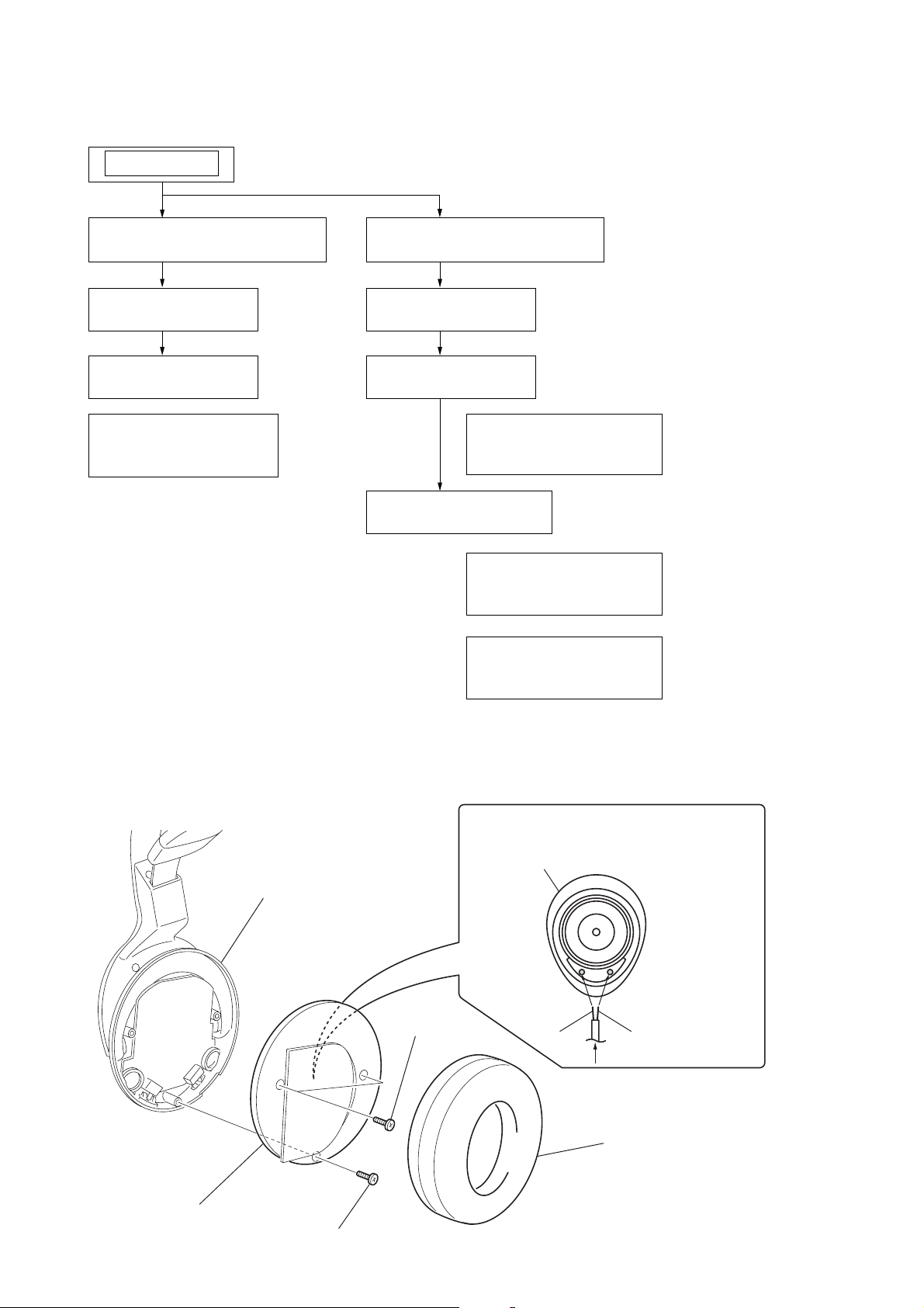
2-1. FRONT PLATE (R) ASSY
(Page 8)
2-2. RX BOARD
(Page 9)
2-3. HANGER (R)
(Page 9)
2-4. WIRING ON THE
RIGHT SIDE
(Page 10)
2-5. FRONT PLATE (L) ASSY
(Page 10)
2-6. BATT BOARD
(Page 11)
2-7. HANGER (L)
(Page 11)
2-8. WIRING ON THE
LEFT SIDE
(Page 12)
2-9. HANGER LID (L)
(Page 12)
2-10. WIRING ON THE
SW BOARD
(Page 13)
2-11. HANG THE
TENSION SPRING
(Page 13)
Note : Follow the disassembly procedure in the numerical order given.
2-1. FRONT PLATE (R) ASSY
4
housing (R) assy
2
P 2.6x6
Removal the solder at 2 places.
Note for installation : Solder the leads at the
driver (R-CH) side
red
places shown below with
attention to their colors.
natural
from RX board
1
ear pad (R)
5
front plate (R) assy
3
P 2.6x6
8
Page 9
2-2. RX BOARD
1
Removal the solder at 12 places.
Note for installation : Solder the leads at the
MDR-IF540R
places shown below with
attention to their colors.
Note : Insert this in the LED hole
in the housing (R) assy
when installing.
2-3. HANGER (R)
housing (R) assy
2
3
S301
RX board
S1
natural
to motor
white
black
red
blue
red
natural
red
G/N
natural
natural
green
to driver
red
1
P 2.6x6
Pay attention to the leads
when assembling.
4
hanger lid (R)
Pay attention to the leads
when assembling.
2
projection
5
3
hanger (R)
9
Page 10

MDR-IF540R
2-4. WIRING ON THE RIGHT SIDE
PD2 board
(R-CH front)
PD1 board
(R-CH rear)
2-5. FRONT PLATE (L) ASSY
housing (L) assy
2
P 2.6x6
4
Removal the solder at 2 places.
Note for installation : Solder the leads at the
driver (L-CH) side
green
1
ear pad (L)
places shown below with
attention to their colors.
natural
from RX board
10
5
front plate (L) assy
3
P 2.6x6
Page 11

2-6. BATT BOARD
housing (L) assy
3
BATT board
2
P 2x6
1
Removal the solder at 8 places.
Note for installation : Solder the leads at the
to motor
blue
G/N
MDR-IF540R
places shown below with
attention to their colors.
natural
red
2-7. HANGER (L)
1
P 2.6x6
black
red
red
red
red
hanger lid (L)
Pay attention to the leads
when assembling.
4
projection
Pay attention to the leads
when assembling.
2
3
5
hanger (L)
11
Page 12

MDR-IF540R
2-8. WIRING ON THE LEFT SIDE
PD2 board
(L-CH rear)
PD1 board
(L-CH front)
2-9. HANGER LID (L)
4
hanger lid (L)
1
P 2.6x6
2
P 2.6x6
3
head band
12
Page 13

2-10. WIRING ON THE SW BOARD
d
SW board
MDR-IF540R
head ban
2-11. HANG THE TENSION SPRING
suspender assy
housing (L) assy
Note for installation : Insert the end of the
hanger lid (L)
tension spring
suspender assy
suspender assy under the
S103 on the SW board.
SW board
S103
13
Page 14

MDR-IF540R
SECTION 3
ELECTRICAL ADJUSTMENTS
PRECAUTION
1. These adjustments should be performed in the order in which
they appear. It is required as a rule to adjust the transmitter
section (TMR-IF540R) before adjusting the headphone
section (MDR-IF540R).
2. Adjustment and measurement should be made on each channel
unless otherwise specified.
3. Adjust on the left channel before adjusting on the right
channel.
4. Supply a power voltage of 9 V to the transmitter section (TMRIF540R) and a power voltage of 2.4 V to the headphones
section (MDR-IF540R).
Headphones Section 0 dBV = 315 mVrms
Note:
1. Use the transmitter section (TMR-IF540R) as a jig for
adjusting the headphones section (MDR-IF540R).
Tuning Adjustment
Preparation:
low-frequency
oscillator
attenuator
1. Apply the input to the jig (TMR-IF540R), and connect a
stabilized power to the DC IN 9V jack (J3).
2. Supply 2.4 V dc between BATT (+) and BATT (–) on the B ATT
board.
3. Set the RV2 (volume control) on the RX board to the minimum
level.
INPUT B
jack (J1)
1 kHz 315 mV (-10 dBV)
jig
transmitter
600
Ω
stabilized
power (9 V dc)
Mute ON Position Adjustment
Preparation:
FM RF
signal generator
10 k
Carrier frequency : 2.8 MHz
Modulation : 1 kHz, 16 kHz deviation
Output level : 34 dB
Connection:
RX board
TP4 (R-ch)
µ
V (EMF)
0.1
Ω
SIG
µ
F
set
TP1 (GND)
level meter
+
Adjustment Method:
1. Connect a level meter to TP4 (R-ch) on the RX board.
2. Short between TP2 and TP3 on the RX board.
3. Write down the reading on the level meter at this time.
4. Remove the short between TP2 and TP3 made in item 2.
5. Adjust the RV1 on the RX board so that the reading on the
level meter is 5 dB to 10 dB below the value written down in
item 3.
Connection:
distortion meter
RX board
TP5 (L-ch)
TP4 (R-ch)
Adjustment Method:
1. Connect a distortion meter to TP5 (L-ch) or TP4 (R-ch) on the
RX board.
2. Adjust the L5 (L-ch) or L6 (R-ch) so as to minimize the
reading on the distortion meter.
L-ch L5 Minimum
R-ch L6 Minimum
100 µF/16 V
+
+
14
Page 15

Adjustment Location:
BATT board (side A) RX board (side B)
MDR-IF540R
BATT (+)
BATT ( )
RV2
VOL
L5
TUNING ADJ
(L-ch)
TP5
(L-ch)
RV1
MUTE ON
POSITION
ADJ
TP4
(R-ch)
TP2
TP3
L6
TUNING ADJ
(R-ch)
RV301
15
Page 16

MDR-IF540R
d
THIS NOTE IS COMMON FOR PRINTED WIRING
BOARDS AND SCHEMATIC DIAGRAMS.
(In addition to this, the necessary note is
printed in each block.)
for schematic diagram:
• All capacitors are in µF unless otherwise noted. pF: µµF
50 WV or less are not indicated except for electrolytics
and tantalums.
• All resistors are in Ω and 1/
specified.
• C : panel designation.
• A : B+ Line.
• H : adjustment for repair.
• Power voltage is dc 2.4 V and fed with regulated dc power
supply from battery terminal.
•Voltage is dc with respect to ground under no-signal
(detuned) conditions.
•Voltages are taken with a VOM (Input impedance 10 MΩ).
Voltage variations may be noted due to normal production tolerances.
• Signal path.
F : ANALOG
J : RF
for printed wiring boards:
• X : parts extracted from the component side.
• Y : parts extracted from the conductor side.
a
•
• : Pattern from the side which enables seeing.
Caution:
Pattern face side: Parts on the pattern face side seen from the
(Side B) pattern face are indicated.
Parts face side: Parts on the parts face side seen from the
(Side A) parts face are indicated.
: Through hole.
(The other layer’s patterns are not indicated.)
4
W or less unless otherwise
SECTION 4
DIAGRAMS
4-1. CIRCUIT BOARDS LOCATION
PD1 board
(R-CH rear)
PD2 board
(R-CH front)
RX board
PD1 board
(L-CH front)
SW board
PD2 board
(L-CH rear)
BATT boar
16
Page 17

4-2. BLOCK DIAGRAM — RECEIVER SECTION —
3 5 6
1
L
R
24
D1
L-CH FRONT
SECTION
D2
L-CH REAR
SECTION
D3
R-CH REAR
SECTION
D4
R-CH FRONT
SECTION
+1.5V
D1-4
IR
RECEIVER
Q1,2
RF AMPQ3BUFFER
L5
(2.3MHz DET)
TUNING
FL1
2.3MHz
BPF
10
DET
DET
20 1322 14 1871615 17 8
FL2
2.8MHz
BPF
L6
(2.8MHz DET)
TUNING
IC1
MIXER/LIMITER/
DEMODULATION
HPF
RV1
MUTE ON
POSITION
1.5V
VCC
VREF
MDR-IF540R
BIAS
EXT
FILTER
IC2
MODE
CONTROL
4
OFF ON
BYPASS
SRS
MATRIX
SRS
BYPASS
MODE
+3.3V
S1
( )
LOUT
ROUT
+V
9
+3.3V
RV2
VOL
7
10
-1
L
-2
R
SRS SURROUND PROCESSOR
11
12
LIN
1
WOUT
2
WIN
3
RIN
16
VREF
15
REFIN
14
V+/2
13
IN1
2
IN2
4
5
REF
IC3
DRIVER AMP
OUT1
OUT2
VCC
+2.4V
+3.3V
9
7
6
+2.4V
MDD1
DRIVER
(L-CH)
MDD2
DRIVER
(R-CH)
CHARGE
TERMINAL
S101
(BATT DET)
(BATT DET)
S102
D101
RECHARGEABLE
BATTERY
(BP-HP550)
1.2V 550mAh
X2
IC101
BATTERY
DOWN
DET
2 1
AUTO ON/OFF
SW103
(AUTO ON/OFF)
Q101,102
IC201
+1.5V
5
REG
1
L101 D102
IC102
+3.3V
SWITCHING REG
Q301
VIBRATION
S301
VIBRATION
OFF
ON
M
M
M301
MOTOR
L-CH
VIBRATION
M302
MOTOR
R-CH
VIBRATION
+2.4V
VCC
4
+1.5V
+3.3V
21
IC303 (1/2)
ADD AMP
6 7 3 1 3 1 10 8
IC303 (2/2)
LPF
RV301
VIBRATION
(VOL)
IC302 (1/4)
BUFFER
IC302 (2/4)
INVERTER
13 14
D302
D303
IC302 (3/4)
COMMUTATION
VCC
FOR IC302
IC304
Q304
BUFFER
IC302 (4/4)
COMPARATOR
6
5
7
Q302
INITIAL
MUTE
Q303
MUTE
-2 -1
MOTOR DRIVE
• Signal path
: ANALOG
: RF
17 17
Page 18

MDR-IF540R
4-3. PRINTED WIRING BOARDS — RECEIVER SECTION (1/2) — • Refer to page 16 for Common Note on Printed Wiring Boards and Circuit Boards Location.
D3
D1-4
IR RECEIVER
D4
B+
SIG
GND
234567891011121314
1
A
MDD2
B
MDD1
C
D
D1
• Semiconductor
Location (Side A)
Ref. No. Location
D1 F-13
D2 F-11
D3 C-13
D4 C-11
E
F
3.3V
D2
G
H
I
M302
(Page 20) (Page 20)
J
1818
Page 19

4-4. PRINTED WIRING BOARD — RECEIVER SECTION (2/2) — • Refer to page 16 for Common Note on Printed Wiring Boards and Circuit Boards Location.
MDR-IF540R
A
B
C
D
E
F
1
234567891011121314
• Semiconductor
Location (Side B)
Ref. No. Location
D201 G-6
D302 E-8
D303 E-8
IC1 D-7
IC2 E-4
IC3 C-4
IC201 H-5
IC302 E-8
IC303 F-6
Q1 B-8
Q2 B-7
Q3 A-6
Q301 G-8
Q302 F-9
Q303 E-9
Q304 E-9
C38
R22
R23
TP7
TP8
R24
C44
C40
R20
C35
C36
C32
C31
C45
IC3
C34
C39
IC2
C30
R25
R21
C33
TP10
C42
C37
R19
R18
R17
C24
C28
C43
C316
R321
FL1
L5
C25
R322
R323
C46
C317
IC303
TP309
C18
R11
C23
L3
C9
R15
C319
C324
C22
R12
R13
C27
TP5
C320
C315
L2
C7
R14
C318
R326
R309
Q3
R325
C6
C10
L4
TP4
R327
IC1
C26
TP6
C312
R318
C311
C5
R6
R5
C1
R315
R314
TP307
R317
C8
R10
Q2
C17
C310
R307
R3
R7
C16
D303
IC302
C308
FL2
L1
R2
R4
C14
C15
R9
R16
R313
C309
Q1
R310
R305
R304
R306
C3
R8
R316
R311
C307
FB1
R312
SIG
C4
C13
RV1
D302
R303
R301
L6
TP305
TP304
C305
B+
C2
R1
TP1
TP2
TP3
Q304
R302
Q303
Q302
G
H
J
RV2
TP9
S1
C29
C203
IC201
C204
C201
C205
C202
R201
C325
D201
C323
C306
Q301
C321
S301
C313
R329
RV301
I
19 19
Page 20

MDR-IF540R
4-5. PRINTED WIRING BOARDS — POWER SECTION (1/2) — • Refer to page 16 for Common Note on Printed Wiring Boards and Circuit Boards Location.
BATT (–)
2345678910111213
1
A
B
C
D
(Page 18)
M301
E
F
G
(Page 18)
BATT (+)
H
I
SW103
J
2020
Page 21

4-6. PRINTED WIRING BOARD — POWER SECTION (2/2) — • Refer to page 16 for Common Note on Printed Wiring Boards and Circuit Boards Location.
MDR-IF540R
A
B
C
D
1
2345678910111213
• Semiconductor
Location (Side B)
Ref. No. Location
D101 C-7
D102 D-6
IC101 C-7
IC102 D-6
Q101 E-7
Q102 C-7
C106
D102
C108
C107
L101
C103
IC102
S102
R103
S101
D101
C102
IC101
Q102
R104
C104
E
F
G
H
C109
C110
R102
C111
C114
R101
Q101
L102
C101
C105
I
J
21 21
Page 22

MDR-IF540R
4-7. SCHEMATIC DIAGRAM — RECEIVER SECTION — • Refer to page 16 for Common Note on Schematic Diagram and page 23 for IC Block Diagrams.
M301
SW103
S101 S102
C105
D4
D3
R101 R102
D101
C101
C102
IC101
C103
TP1
Q101
D102
L101 L102
C104
R103
Q102
R104
C106
C1
R1
C3
FB1
C2
C4L1
IC102
C107
R4
R2
Q1
R3
TP102
C5
TP101
C108
C109
C110
C111
C114
C201
C202
D201
R201
IC201
C203 C204
C205
S1
C28 C29
R19
C31
C30
C32
IC B/D
C15
RV1
C13
C14
C22
R8 R9
TP3
TP2
R12
C23
IC2
C17C16
R10
IC1
R14
R15
L6L5
R13
R17
18
R
C34
C33
R22
C24
TP4
TP5
R16
C26
C35 C36
C25
TP7 TP8
RV2
C27
TP6
R20
C40
R21
C39
C37
TP9
C38
IC3
IC B/D
C317C316
R23
C42
C43
R24 R25
C44
MDD1
MDD2
C46
C45
TP10
FL2
R7
L2
R5
C6
Q3
C7
L3
R6
Q2
C8
C9
C10
L4
C18
R11
FL1
TP309
R321 R322
R323
IC303
C318
R326 R327
C319 C320
TP310
C306
R301
TP304
D2
D1
M302
C323
C324 C325
S301
Q301
C321
Q302
C305
TP303
R302
Q303
Q304
R303
R305
R304
307
C
TP305
R311
D302
TP306
R306
R310
R312
R307
TP307
IC302
R315
R314
C309
C310
R316
D303
313
R
C308
R317 R318
C311
R309
C312 C313
R329
C315
TP308
R325
RV301
2222
Page 23

4-8. IC BLOCK DIAGRAMS
IC2 NJM2190V(TE2)
MDR-IF540R
POWER SWITCH
VREF
WOUT
REFIN
WIN
MODE
CONTROL
RIN
–
+
1 52 3 4 6 7 8
LIN
V+/2
FILTER
MODE
EXT
C4
C1
BYPASS
SRS
MATRIX
SRS
BYPASS
IC3 LA4533M-TE-L
POWER
1
SWITCH
MUTE
CIRCUIT
10
MUTE SWITCH
C3
ROUT
V+
9
10111213141516
BIAS
C2
LOUT
GND
IN-1
PRE-GND
IN-2
REF
2
3
4
BIAS
5
AMP 1
AMP 2
9
OUT-1
8
POWER GND
7
OUT-2
6
VCC
23
Page 24

MDR-IF540R
NOTE:
• The mechanical parts with no reference
number in the exploded views are not supplied.
• Items marked “*” are not stocked since
they are seldom required for routine service.
Some delay should be anticipated
when ordering these items.
5-1. HOUSING (L) ASSY SECTION
2
SECTION 5
EXPLODED VIEWS
• -XX and -X mean standardized parts, so
they may have some difference from the
original one.
• Color Indication of Appearance Parts
Example :
KNOB, BALANCE (WHITE) ... (RED)
R
Parts Color Cabinet’s Color
• Accessories are given in the last of this parts list.
R
not supplied
(SW board)
#2
#2
not supplied
MDD1
11
#1
A
10
#2
#2
not supplied
(PD1 board)
9
A
B
B
6
4
not supplied
5
(PD2 board)
3
7
not
supplied
8
1
Ref. No. Part No. Description Remark
1 A-3229-743-A LID ASSY, BATTERY CASE
2 3-246-153-01 PAD (L), EAR
3 3-246-148-01 BUTTON
4 3-246-140-01 LID (L), HANGER
5 3-246-138-01 HANGER (L)
6 4-213-918-11 SPRING, TENSION
7 3-246-151-01 TERMINAL (–), BATTERY
24
Ref. No. Part No. Description Remark
8 3-246-150-01 TERMINAL (+), BATTERY
* 9 A-3347-241-A BATT BOARD, COMPLETE
10 3-246-152-01 TERMINAL, CHARGE
11 A-3229-744-A PLATE (L) ASSY, FRONT
MDD1 1-542-400-11 DRIVER (030F032) (L-CH)
#1 7-685-104-19 SCREW +P 2X6 TYPE2 NON-SLIT
#2 7-685-133-19 SCREW +P 2.6X6 TYPE2 NON-SLIT
Page 25

5-2. HOUSING (R) ASSY SECTION
60
58
not supplied
(PD1 board)
MDR-IF540R
61
not supplied
(PD2 board)
57
56
59
not
supplied
55
#2
#2
54
not
supplied
53
62
64
#2
MDD2
not supplied
63
63
64
not
supplied
62
52
51
#2
#2
Ref. No. Part No. Description Remark Ref. No. Part No. Description Remark
51 3-246-154-01 PAD (R), EAR
52 A-3229-745-A PLATE (R) ASSY, FRONT
* 53 A-3347-237-A RX BOARD, COMPLETE
54 3-246-149-01 KNOB (SURROUND)
55 3-246-955-01 KNOB (VIBRATION)
56 3-246-954-01 GRILLE (R)
57 3-246-156-01 CAP (R), HOUSING
58 3-246-139-01 HANGER (R)
59 3-246-141-01 LID (R), HANGER
60 3-246-137-01 BAND, HEAD
61 A-3229-747-A SUSPENDER ASSY
62 4-966-791-01 STOPPER (UPPER)
63 4-966-792-01 STOPPER (LOWER)
64 3-318-203-62 SCREW (B1.7X4), TAPPING
MDD2 1-542-400-11 DRIVER (030F032) (R-CH)
#2 7-685-133-19 SCREW +P 2.6X6 TYPE2 NON-SLIT
25
Page 26

MDR-IF540R
PD2PD1BATT
SECTION 6
ELECTRICAL PARTS LIST
RX
NOTE:
• Due to standardization, replacements in
the parts list may be different from the
parts specified in the diagrams or the
components used on the set.
• -XX and -X mean standardized parts, so
they may have some difference from the
original one.
• RESISTORS
All resistors are in ohms.
METAL:Metal-film resistor.
METAL OXIDE: Metal oxide-film resistor.
F:nonflammable
Ref. No. Part No. Description Remark Ref. No. Part No. Description Remark
* A-3347-241-A BATT BOARD, COMPLETE
*********************
< CAPACITOR >
C101 1-126-209-11 ELECT CHIP 100uF 20% 4V
C102 1-162-970-11 CERAMIC CHIP 0.01uF 10% 25V
C103 1-162-970-11 CERAMIC CHIP 0.01uF 10% 25V
C104 1-162-970-11 CERAMIC CHIP 0.01uF 10% 25V
C105 1-107-826-11 CERAMIC CHIP 0.1uF 10% 16V
C106 1-126-209-11 ELECT CHIP 100uF 20% 4V
C107 1-125-837-11 CERAMIC CHIP 1uF 10% 6.3V
C108 1-107-826-11 CERAMIC CHIP 0.1uF 10% 16V
C109 1-126-209-11 ELECT CHIP 100uF 20% 4V
C110 1-126-607-11 ELECT CHIP 47uF 20% 4V
• Items marked “*” are not stocked since
they are seldom required for routine service.
Some delay should be anticipated
when ordering these items.
• SEMICONDUCTORS
In each case, u : µ, for example:
uA.. : µA.. uPA.. : µPA..
uPB.. : µPB.. uPC.. : µPC.. uPD.. : µPD..
• CAPACITORS
uF : µF
• COILS
uH : µH
S102 1-762-944-21 SWITCH, DETECTION (SMALL TYPE)
*************************************************************
D1 8-719-058-49 PHOTO SENSOR PP508
*************************************************************
When indicating parts by reference
number, please include the board.
(BATT DET)
PD1 BOARD (L-CH FRONT)
**********
< PHOTO SENSOR >
PD1 BOARD (R-CH REAR)
**********
< PHOTO SENSOR >
C111 1-107-826-11 CERAMIC CHIP 0.1uF 10% 16V
C114 1-107-826-11 CERAMIC CHIP 0.1uF 10% 16V
< DIODE >
D101 8-719-071-34 DIODE RB521S-30-TE61
D102 8-719-072-27 DIODE MA2Z748001S0
< IC >
IC101 6-702-083-01 IC XC61CN1902NR
IC102 8-759-571-29 IC XC6371A331PR
< COIL >
L101 1-414-404-41 INDUCTOR 100uH
L102 1-414-404-41 INDUCTOR 100uH
< TRANSISTOR >
Q101 6-550-363-01 TRANSISTOR 2SB1690KT146
Q102 8-729-230-49 TRANSISTOR 2SC2712-YG
< RESISTOR >
R101 1-216-845-11 METAL CHIP 100K 5% 1/10W
R102 1-216-833-11 METAL CHIP 10K 5% 1/10W
R103 1-216-821-11 METAL CHIP 1K 5% 1/10W
R104 1-216-857-11 METAL CHIP 1M 5% 1/10W
D3 8-719-058-49 PHOTO SENSOR PP508
*************************************************************
PD2 BOARD (L-CH REAR)
**********
< PHOTO SENSOR >
D2 8-719-058-49 PHOTO SENSOR PP508
*************************************************************
PD2 BOARD (R-CH FRONT)
**********
< PHOTO SENSOR >
D4 8-719-058-49 PHOTO SENSOR PP508
*************************************************************
* A-3347-237-A RX BOARD, COMPLETE
*******************
< CAPACITOR >
C1 1-126-607-11 ELECT CHIP 47uF 20% 4V
C2 1-162-970-11 CERAMIC CHIP 0.01uF 10% 25V
C3 1-162-970-11 CERAMIC CHIP 0.01uF 10% 25V
C4 1-164-160-11 CERAMIC CHIP 20PF 5% 50V
C5 1-107-826-11 CERAMIC CHIP 0.1uF 10% 16V
< SWITCH >
S101 1-762-742-61 SWITCH, DETECTION (SMALL TYPE)
26
(BATT DET)
C6 1-164-385-11 CERAMIC CHIP 160PF 5% 50V
C7 1-162-926-11 CERAMIC CHIP 82PF 5% 50V
C8 1-107-826-11 CERAMIC CHIP 0.1uF 10% 16V
C9 1-107-826-11 CERAMIC CHIP 0.1uF 10% 16V
C10 1-107-826-11 CERAMIC CHIP 0.1uF 10% 16V
Page 27

MDR-IF540R
RX
Ref. No. Part No. Description Remark Ref. No. Part No. Description Remark
C13 1-126-607-11 ELECT CHIP 47uF 20% 4V
C14 1-162-970-11 CERAMIC CHIP 0.01uF 10% 25V
C15 1-162-959-11 CERAMIC CHIP 330PF 5% 50V
C16 1-164-217-11 CERAMIC CHIP 150PF 5% 50V
C17 1-164-217-11 CERAMIC CHIP 150PF 5% 50V
D303 8-719-070-20 DIODE RB706F-40
< FERRITE BEAD >
FB1 1-414-229-11 INDUCTOR, FERRITE BEAD
C18 1-162-924-11 CERAMIC CHIP 56PF 5% 50V
C22 1-164-739-11 CERAMIC CHIP 560PF 5% 50V
C23 1-125-837-11 CERAMIC CHIP 1uF 10% 6.3V
C24 1-125-837-11 CERAMIC CHIP 1uF 10% 6.3V
C25 1-125-837-11 CERAMIC CHIP 1uF 10% 6.3V
C26 1-110-563-11 CERAMIC CHIP 0.068uF 10% 16V
C27 1-110-563-11 CERAMIC CHIP 0.068uF 10% 16V
C28 1-128-993-21 ELECT CHIP 22uF 20% 10V
C29 1-124-779-00 ELECT CHIP 10uF 20% 16V
C30 1-162-968-11 CERAMIC CHIP 0.0047uF 10% 50V
C31 1-128-993-21 ELECT CHIP 22uF 20% 10V
C32 1-162-970-11 CERAMIC CHIP 0.01uF 10% 25V
C33 1-162-967-11 CERAMIC CHIP 0.0033uF 10% 50V
C34 1-107-826-11 CERAMIC CHIP 0.1uF 10% 16V
C35 1-125-837-11 CERAMIC CHIP 1uF 10% 6.3V
C36 1-125-837-11 CERAMIC CHIP 1uF 10% 6.3V
C37 1-162-964-11 CERAMIC CHIP 0.001uF 10% 50V
C38 1-126-393-11 ELECT CHIP 33uF 20% 10V
C39 1-162-927-11 CERAMIC CHIP 100PF 5% 50V
C40 1-162-927-11 CERAMIC CHIP 100PF 5% 50V
C42 1-162-970-11 CERAMIC CHIP 0.01uF 10% 25V
C43 1-126-607-11 ELECT CHIP 47uF 20% 4V
C44 1-107-826-11 CERAMIC CHIP 0.1uF 10% 16V
C45 1-107-826-11 CERAMIC CHIP 0.1uF 10% 16V
C46 1-126-246-11 ELECT CHIP 220uF 20% 4V
C201 1-126-209-11 ELECT CHIP 100uF 20% 4V
C202 1-107-826-11 CERAMIC CHIP 0.1uF 10% 16V
C203 1-115-467-11 CERAMIC CHIP 0.22uF 10% 10V
C204 1-162-970-11 CERAMIC CHIP 0.01uF 10% 25V
C205 1-115-467-11 CERAMIC CHIP 0.22uF 10% 10V
< BPF >
FL1 1-239-762-11 FILTER, BAND PASS
FL2 1-239-763-11 FILTER, BAND PASS
< IC >
IC1 8-759-364-96 IC TA2056FN-EL
IC2 8-759-597-24 IC NJM2190V(TE2)
IC3 8-759-714-80 IC LA4533M-TE-L
IC201 6-703-086-01 IC TK11115CSCL-G
IC302 8-759-594-39 IC LMV324MTX
IC303 8-759-370-11 IC NJM2100V-TE2
< COIL >
L1 1-412-955-11 INDUCTOR 22uH
L2 1-412-957-11 INDUCTOR 33uH
L3 1-412-957-11 INDUCTOR 33uH
L4 1-412-958-21 INDUCTOR 39uH
L5 1-411-530-21 COIL (DET)
L6 1-411-531-21 COIL (DET)
< TRANSISTOR >
Q1 8-729-220-93 FET 2SK209-G
Q2 8-729-230-49 TRANSISTOR 2SC2712-YG
Q3 8-729-230-49 TRANSISTOR 2SC2712-YG
Q301 6-550-364-01 TRANSISTOR 2SD2652T106
Q302 8-729-029-14 TRANSISTOR DTC144EUA-T106
Q303 8-729-029-14 TRANSISTOR DTC144EUA-T106
Q304 8-729-037-53 TRANSISTOR 2SB1462J-QR(TX)
C305 1-125-889-11 CERAMIC CHIP 2.2uF 10% 10V
C306 1-128-993-21 ELECT CHIP 22uF 20% 10V
C307 1-162-970-11 CERAMIC CHIP 0.01uF 10% 25V
C308 1-162-970-11 CERAMIC CHIP 0.01uF 10% 25V
C309 1-125-889-11 CERAMIC CHIP 2.2uF 10% 10V
C310 1-125-889-11 CERAMIC CHIP 2.2uF 10% 10V
C311 1-115-467-11 CERAMIC CHIP 0.22uF 10% 10V
C312 1-125-889-11 CERAMIC CHIP 2.2uF 10% 10V
C313 1-125-889-11 CERAMIC CHIP 2.2uF 10% 10V
C315 1-162-970-11 CERAMIC CHIP 0.01uF 10% 25V
C316 1-125-837-11 CERAMIC CHIP 1uF 10% 6.3V
C317 1-125-837-11 CERAMIC CHIP 1uF 10% 6.3V
C318 1-165-176-11 CERAMIC CHIP 0.047uF 10% 16V
C319 1-115-467-11 CERAMIC CHIP 0.22uF 10% 10V
C320 1-162-970-11 CERAMIC CHIP 0.01uF 10% 25V
C321 1-107-826-11 CERAMIC CHIP 0.1uF 10% 16V
C323 1-107-826-11 CERAMIC CHIP 0.1uF 10% 16V
C324 1-126-607-11 ELECT CHIP 47uF 20% 4V
C325 1-107-826-11 CERAMIC CHIP 0.1uF 10% 16V
< DIODE >
D201 8-719-066-57 LED SA2512 (POWER)
D302 8-719-070-20 DIODE RB706F-40
< RESISTOR >
R1 1-216-823-11 METAL CHIP 1.5K 5% 1/10W
R2 1-216-841-11 METAL CHIP 47K 5% 1/10W
R3 1-216-821-11 METAL CHIP 1K 5% 1/10W
R4 1-216-823-11 METAL CHIP 1.5K 5% 1/10W
R5 1-216-837-11 METAL CHIP 22K 5% 1/10W
R6 1-216-818-11 METAL CHIP 560 5% 1/10W
R7 1-216-827-11 METAL CHIP 3.3K 5% 1/10W
R8 1-216-833-11 METAL CHIP 10K 5% 1/10W
R9 1-216-839-11 METAL CHIP 33K 5% 1/10W
R10 1-216-839-11 METAL CHIP 33K 5% 1/10W
R11 1-216-827-11 METAL CHIP 3.3K 5% 1/10W
R12 1-220-158-11 METAL CHIP 3.6K 5% 1/10W
R13 1-216-826-11 METAL CHIP 2.7K 5% 1/10W
R14 1-216-809-11 METAL CHIP 100 5% 1/10W
R15 1-216-809-11 METAL CHIP 100 5% 1/10W
R16 1-216-826-11 METAL CHIP 2.7K 5% 1/10W
R17 1-216-840-11 METAL CHIP 39K 5% 1/10W
R18 1-216-837-11 METAL CHIP 22K 5% 1/10W
R19 1-216-809-11 METAL CHIP 100 5% 1/10W
R20 1-216-825-11 METAL CHIP 2.2K 5% 1/10W
R21 1-216-825-11 METAL CHIP 2.2K 5% 1/10W
27
Page 28

MDR-IF540R
RX SW
Ref. No. Part No. Description Remark
R22 1-216-837-11 METAL CHIP 22K 5% 1/10W
R23 1-216-839-11 METAL CHIP 33K 5% 1/10W
R24 1-216-797-11 METAL CHIP 10 5% 1/10W
R25 1-216-797-11 METAL CHIP 10 5% 1/10W
R201 1-216-821-11 METAL CHIP 1K 5% 1/10W
R301 1-216-805-11 METAL CHIP 47 5% 1/10W
R302 1-216-821-11 METAL CHIP 1K 5% 1/10W
R303 1-216-833-11 METAL CHIP 10K 5% 1/10W
R304 1-216-845-11 METAL CHIP 100K 5% 1/10W
R305 1-216-845-11 METAL CHIP 100K 5% 1/10W
R306 1-216-857-11 METAL CHIP 1M 5% 1/10W
R307 1-216-852-11 METAL CHIP 390K 5% 1/10W
R309 1-216-841-11 METAL CHIP 47K 5% 1/10W
R310 1-216-837-11 METAL CHIP 22K 5% 1/10W
R311 1-216-845-11 METAL CHIP 100K 5% 1/10W
R312 1-216-837-11 METAL CHIP 22K 5% 1/10W
R313 1-216-845-11 METAL CHIP 100K 5% 1/10W
R314 1-216-833-11 METAL CHIP 10K 5% 1/10W
R315 1-216-833-11 METAL CHIP 10K 5% 1/10W
R316 1-216-837-11 METAL CHIP 22K 5% 1/10W
R317 1-216-833-11 METAL CHIP 10K 5% 1/10W
R318 1-216-841-11 METAL CHIP 47K 5% 1/10W
R321 1-216-837-11 METAL CHIP 22K 5% 1/10W
R322 1-216-837-11 METAL CHIP 22K 5% 1/10W
R323 1-216-845-11 METAL CHIP 100K 5% 1/10W
R325 1-218-867-11 METAL CHIP 6.8K 5% 1/10W
R326 1-216-843-11 METAL CHIP 68K 5% 1/10W
R327 1-216-843-11 METAL CHIP 68K 5% 1/10W
R329 1-216-821-11 METAL CHIP 1K 5% 1/10W
< VARIABLE RESISTOR >
RV1 1-223-274-11 RES, ADJ, CERMET (3 TYPE) 2.2K
RV2 1-227-536-11 RES, VAR, CARBON 50KX2 (VOL)
RV301 1-227-524-11 RES, VER, CARBON 50KX2 (VIBRATION (VOL))
< SWITCH >
S1 1-571-478-11 SWITCH, SLIDE ((z))
S301 1-571-478-11 SWITCH, SLIDE (VIBRATION)
*************************************************************
SW BOARD
**********
< SWITCH >
SW103 1-762-003-11 SWITCH, PUSH (AUTO ON/OFF)
*************************************************************
MISCELLANEOUS
***************
MDD1 1-542-400-11 DRIVER (030F032) (L-CH)
MDD2 1-542-400-11 DRIVER (030F032) (R-CH)
28
Page 29

MEMO
MDR-IF540R
29
Page 30

MDR-IF540R
REVISION HISTORY
Clicking the version allows you to jump to the revised page.
Also, clicking the version at the upper right on the revised page allows you to jump to the next revised
page.
Ver. Date Description of Revision
1.0 2003. 03 New
30
 Loading...