

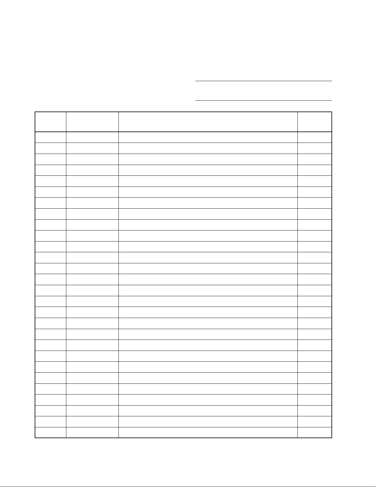
SONY KV-DX32K9H, KV-DX32K9B, KV-DX32K90B, KV-DX32K90L Service Manual
HISTORY
When clicking an item, it’s detail is displayed.
Model Name: KV-DX32K9H/DX32K9H/B/
DX32K90B/DX32K90L
SERVICE MANUAL
Part No. : 9-965-363-02
Date SUPP./CORR. Description of SUP/COR
2003.05 NEW –
2004.06 Revised KV-DX32K90B/DX32K90L Models Addition Yes
Change of
main text
SERVICE MANUAL
DX-1J
CHASSIS
MODEL COMMANDER DEST. CHASSIS NO.
–––––– –––––––––––– ––––– –––––––––––
KV-DX32K9H RM-1006 Korean SCC-P81F-A
KV-DX32K9H/B
KV-DX32K90B RM-1006 Korean SCC-P81I-A
KV-DX32K90L RM-1006 Korean SCC-P81L-A
RM-1006 Korean SCC-P81F-A
MODEL COMMANDER DEST. CHASSIS NO.
–––––– –––––––––––– ––––– –––––––––––
RM-1006
KV-DX32K9H/KV-DX32K9H/B/DX32K90B/DX32K90L
TRINITRON COLOR TV
R
KV-DX32K9H/DX32K9H/B/DX32K90B/DX32K90L
RM-1006 RM-1006 RM-1006 RM-1006
Specifications
Antenna 75 ohm external terminal for VHF/UHF
Television System NTSC, American TV Standard
Screen Size (measured diagonally) 32 inches
Channel Coverage
VHF 2-13
UHF 14-69
CATV 1-125
Power Requirements
Number of Inputs/Outputs
Vid eo (IN) 4 1 Vp-p, 75 ohms unbalanced, sync negative
S Video (IN) 3 Y: 1 Vp-p, 75 ohms unbalanced, sync negative
Audio (IN) 6 500 mVrms (100% modulation)
TV Out 1 Video: 1 Vp-p 75 ohms unbalanced, Sync
DTV (HD)/DVD Input 2 (Y, P
RF Inputs 1
Converter 1
Speaker Output 5 W x 2, 10W x 1
Dimensions (W x H x D) 882 x 590 x 549 mm
Mass 66.7 kg
Power Consumption
Design and specifications are subject to change without notice.
220 V AC, 60 Hz
, PR)Y: 1.0 Vp-p, 75 ohms unbalanced, sync
B
Indicated on the rear of the TV
C: 0.286 Vp-p (Burst signal), 75 ohms
Impedance: 47 kiloohms
negative
Audio: 500 mVrms
negative
P
: 0.7 Vp-p, 75 ohms
B
PR: 0.7 Vp-p, 75 ohms
– 2 –

KV-DX32K9H/DX32K9H/B/DX32K90B/DX32K90L
RM-1006 RM-1006 RM-1006 RM-1006
SHORT CIRCUIT THE ANODE OF THE PICTURE TUBE AND THE
ANODE CAP TO THE METAL CHASSIS, CRT SHIELD, OR CARBON PAINTED ON THE CRT, AFTER REMOVING THE ANODE.
AN ISOLATION TRANSFORMER SHOULD BE USED DURING
ANY SERVICE TO AVOID POSSIBLE SHOCK HAZARD, BECAUSE OF LIVE CHASSIS.
THE CHASSIS OF THIS RECElVER IS DIRECTLY CONNECTED
TO THE AC POWER LINE.
SAFETY-RELATED COMPONENT WARNING!!
COMPONENTS IDENTIFIED BY SHADING AND MARK ! ON
THE SCHEMATIC DIAGRAMS, EXPLODED VIEWS AND IN THE
PAR TS LIST ARE CRITICAL TO SAFE OPERATION. REPLACE
THESECOMPONENTS WITH SONY PARTS WHOSE PART NUMBERS APPEAR AS SHOWN IN THIS MANUAL OR IN SUPPLEMENTS PUBLISHED BY SONY. CIRCUIT ADJUSTMENTS THAT
ARE CRITICAL TO SAFEOPERATION ARE IDENTIFIED IN THIS
MANUAL. FOLLOW THESE PROCEDURES WHENEVER CRITICAL COMPONENTS ARE REPLACED OR IMPROPER OPERATION IS SUSPECTED.
(CAUTION)
WARNING!!
– 3 –

KV-DX32K9H/DX32K9H/B/DX32K90B/DX32K90L
RM-1006 RM-1006 RM-1006 RM-1006
TABLE OF CONTENTS
Section Title Page
–––––– –––– ––––
1. SELF DIAGNOSIS FUNCTION .................................... 5
2. DISASSEMBLY
2-1. REAR COVER ............................................................ 8
2-2. SPEAKER BLOCK .................................................... 8
2-3. CHASSIS ASSEMBLY ............................................... 9
2-4. ASSEMBLING CHASSIS ASSEMBLY .................. 10
2-5. SERVICE POSITION ............................................... 11
2-6. U BRACKET ............................................................ 11
2-7. F4 BOARD ................................................................ 12
2-8. U3 BOARD ............................................................... 12
2-9. B1 BOARD ............................................................... 13
2-10. H1 BOARD ............................................................... 13
2-11. H2 BOARD ............................................................... 14
2-12. H4 BOARD ............................................................... 14
2-13. REMOVAL OF ANODE-CAP .................................. 15
2-14. CRT ........................................................................... 16
2-15. PARTS LOCATION AND WIRING ......................... 17
3. SERVICE MODE
Section Title Page
–––––– –––– ––––
5. SAFETY RELATED ADJUSTMENTS
5-1. +B MAX VOLTAGE CONFIRMATION .................. 52
5-2. HV REGULATION CIRCUIT ADJUSTMENT ....... 52
5-3. HV PROTECTOR CIRCUIT ADJUSTMENT ......... 52
5-4. IK PROTECTOR CIRCUIT CHECK (D BOARD).. 52
6. DIAGRAMS
6-1. BLOCK DIAGRAM (1) ............................................ 53
BLOCK DIAGRAM (2) ............................................ 55
BLOCK DIAGRAM (3) ............................................ 57
BLOCK DIAGRAM (4) ............................................ 59
BLOCK DIAGRAM (5) ............................................ 61
BLOCK DIAGRAM (6) ............................................ 63
BLOCK DIAGRAM (7) ............................................ 65
6-2. CIRCUIT BOARDS LOCATION ................................. 68
6-3. PRINTED WIRING BOARDS AND SCHEMATIC
DIAGRAMS................................................................... 68
6-4. SEMICONDUCTORS ................................................. 139
3-1. METHOD OF SETTING THE SERVICE
ADJUSTMENT MODE ............................................ 18
3-2. SERVICE MODE ADJUSTMENT ........................... 18
3-3. MEMORY WRITE CONFIRMATION METHOD .. 18
3-4. ADJUSTING BUTTONS AND INDICATOR.......... 18
3-5. SERVICE MODE LIST ............................................ 19
4. SET-UP ADJUSTMENTS
4-1. BEAM LANDING .................................................... 46
4-2. CONVERGENCE ADJUSTMENT .......................... 47
4-3. G2 (SCREEN) ADJUSTMENT ................................ 49
4-4. FOCUS ADJUSTMENT 1 ........................................ 49
4-5. NECK ASSY TWIST AJUSTMENT ........................ 49
4-6. P&P SUB CONTRAST ADJUSTMENT
(VIDEO) (SCON) ..................................................... 50
4-7. P&P SUB CONTRAST ADJUSTMENT
(RF) (SCON) ............................................................. 50
4-8. P&P SUB-HUE AND SUB-COLOR
ADJUSTMENT (VIDEO) (SHUE, SCOL) .............. 50
4-9. P&P SUB-HUE AND SUB-COLOR
ADJUSTMENT (RF) (SHUE, SCOL) ...................... 50
4-10. WHITE BALANCE, SUB BRIGHT
ADJUSTMENT ......................................................... 51
4-11. FOCUS ADJUSTMENT 2 ........................................ 51
4-12. PICTURE DISTORTION ADJUSTMENT .............. 51
7. EXPLODED VIEWS
7-1. SPEAKER SECTION ............................................. 141
7-2. CHASSIS SECTION .............................................. 142
7-3. BEZNET SECTION ................................................ 143
7-4. CRT SECTION ....................................................... 144
8. ELECTRICAL PARTS LIST..................................... 145
– 4 –
KV-DX32K9H/DX32K9H/B/DX32K90B/DX32K90L
RM-1006 RM-1006 RM-1006 RM-1006
SECTION 1
SELF DIAGNOSIS FUNCTION
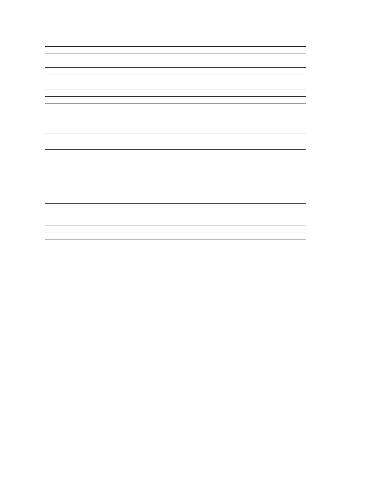
1. Summary of Self-Diagnosis Function
• This device includes a self-diagnosis function.
• In case of abnormalities, the STANDBY/ indicator automatically blinks. It is possible to predict the abnormality
location by the number of blinks. The Instruction Manual describes blinking of the /STANDBY/ indicator.
• If the symptom is not reproduced sometimes in case of a malfunction, there is recording of whether a malfunction was generated
or not. Operate the remote command to confirm the matter on the screen and to predict the location of the abnormality.
2. Diagnosis Items and Prediction of Malfunction Location
• When a malfunction occurs the STANDBY/ indicator only blinks for one of the following diagnosis items. In case of
two or more malfunctions, the item which first occurred blinks. If the malfunctions occurred simultaneously, the item with the
lower blink count blinks first.
• The screen display displays the results regarding all the diagnosis items listed below. The display “ 0 ” means that no malfunctions occurred.
Number of times
Diagnosis Item
+B overcurrent (OCP)
+B overvoltage (OVP)
Vertical deflection stopped
(V-STOP)
IK error (AKB ERROR)
Low-B error
STANDBY/
indicator blinks
2 times
3 times
4 times
5 times
6 times
Probable Cause Location
T8001 (FBT) Rare short-circuit etc. (D6 board)
Q5030 (H-OUT), Q5028 (D6 board)
+B load open (D6 board) R6570 Open
PH6502, control system malfunction L2603
Open
IC5004 (V. OUT) (D6 board) IC201
(CXA2150Q) (A6 board)
VIDEO OUT IC malfunction IC9001, 9002,
9003 (C3 board) IC201 (CXA2150Q)
(A6 board)
Sub power supply system load shorted etc.
(A6 board)
Detected Symptoms
Has entered standby mode.
(Relay is off when the power
turns on.)
Has entered standby mode.
Has entered standby mode.
Has not entered standby mode.
Has entered standby mode.
Horizontal deflection
stopped (H-STOP)
7 times
IC201 (CXA2150Q) (A6 board) Q5031
(S-COR-OUT), Q5030 (H-OUT), Q5028
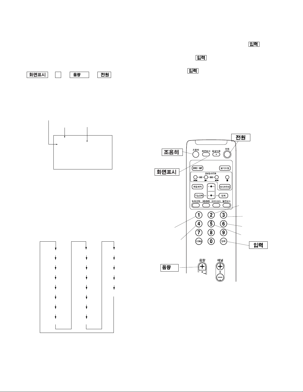
3. Blinking count display of STANDBY/ indicator
< FRONT PANEL >
STANDBY/ indicator
Release of STANDBY/ indicator blinking.
• The STAND BY indicator blinking display is released by turning OFF the power switch
on the TV main unit or removing the plug from the power.
* One blink is not used for self-diagnosis.
¥EXAMPLE
<Diagnosis Items> <Number of Blinks>
¥ +B overcurrent 2 times
¥ +B overvoltage 3 times
¥ Vertical deflection stop 4 times
Lamp ON : 0.3 seconds
Lamp OFF : 0.3 seconds
Has entered standby mode.
Lamp OFF :
3.0 seconds
– 5 –
KV-DX32K9H/DX32K9H/B/DX32K90B/DX32K90L
RM-1006 RM-1006 RM-1006 RM-1006
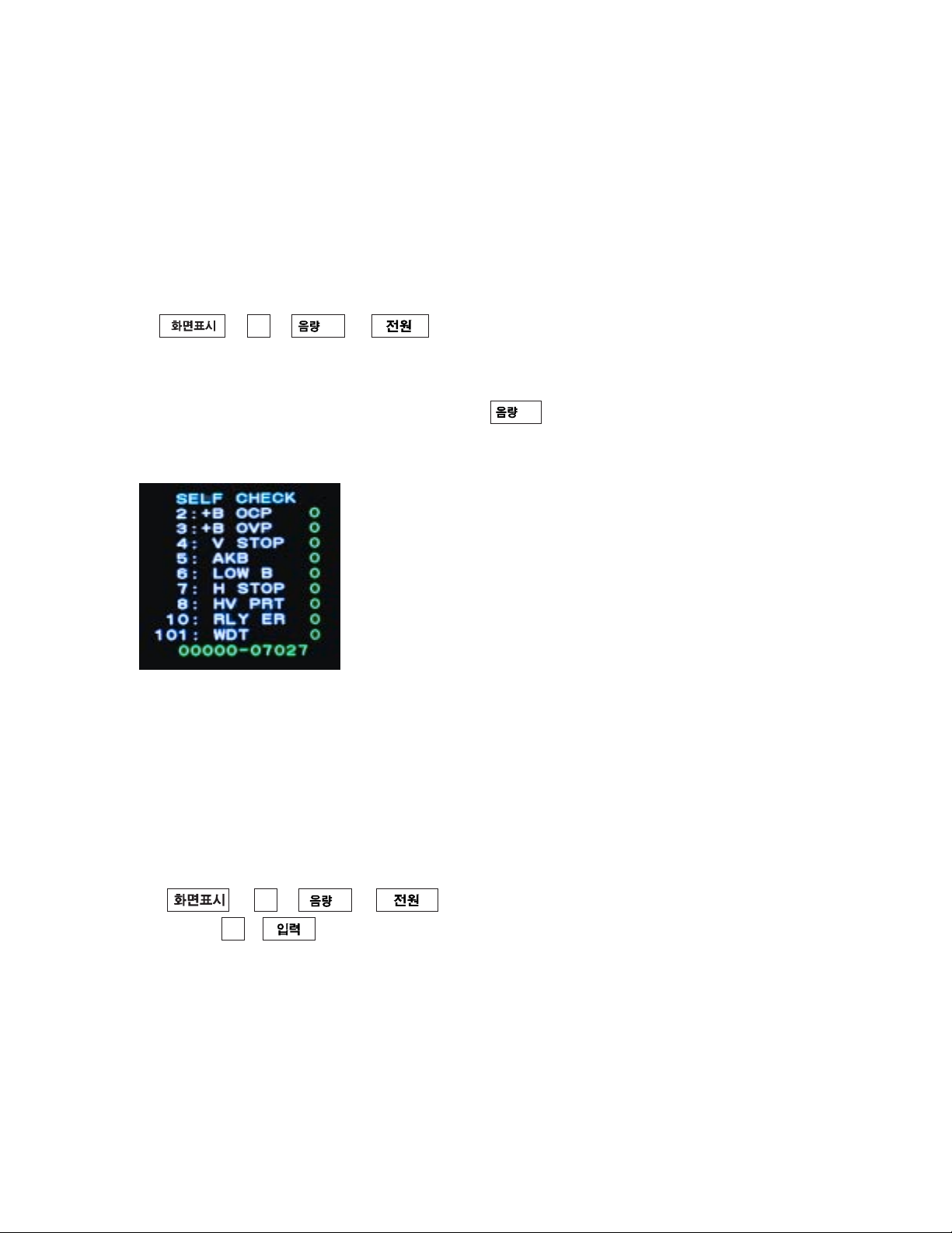
4. Self-diagnosis screen displays
• In cases of malfunctions where it is not possible to determine the symptom such as when the power goes off occasionally or when
the screen disappears occasionally, there is a screen display on whether the malfunction occurred or not in the past (and whether
the detection circuit operated or not) in order to allow confirmation.
<Screen Display Method>
• Quickly press the remote command button in the following order from the standby state.
5
b b b
–
˘
Be aware that this differs from the method of
entering the service mode ( + ).
Self-diagnosis screen display
• "G" : OK, "NG" : DETECTS ONCE OR MORE
• THE 10 DIGITS OF NUMERALS ARE FOR CHECKING,
NO RELATION TO DIAGNOSIS.
• 101 : NO LED BLINKING FOR WDT.
"0" : NUMBER OF DETECTION.
5. After the self-diagnosis operation
• The results display is not automatically cleared. In case of repairs and after repairs, check the self-diagnosis screen and be sure
to return the results display to “ 0 ”.
• If the results display is not returned to “ 0 ” it will not be possible to judge a new malfunction after completing repairs.
<Method of Clearing Results Display>
1. Power off (Set to the standby mode)
2. b 5 b + b (Service Mode)
3. Channel 8 b (Test reset = Factory preset condition)
<Method of Ending Self Diagnosis Screen>
• When ending the self-diagnosis screen completely, turn the power switch OFF on the remote commander or the main unit.
– 6 –
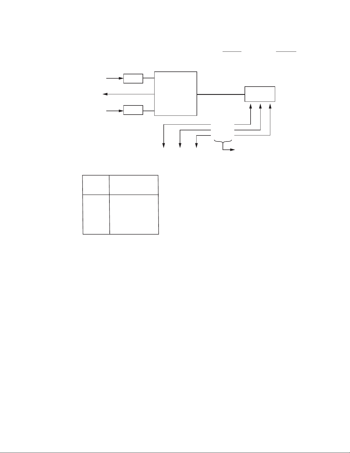
KV-DX32K9H/DX32K9H/B/DX32K90B/DX32K90L
Q727
Q729
OVP
(FROM D BOARD)
AC-RLY
(TO D BOARD)
OCP
(FROM D BOARD)
• I2C YCJ RETURN DATA
11111111
LED
BLINKING
TIMES
2
3
4
5
6
7
LATCH
LATCH
Q726
Q728
SYMPTOM
+B OCP
+B OVP
V-STOP
AKB
LOW-B ERROR
H-STOP
OVP
MAIN
MICROCOMPUTER
IC701
M308V2
OCP
RM-1006 RM-1006 RM-1006 RM-1006
A1 BOARD
12C BUS
A K B
H-STOP
V-STOP
YCJ IC201
CXA-2150Q
WHEN
A K B
H-STOP
V-STOP
ARE ALL 1= LOW B ERROR
+B OCP If the IC701 Pin 44 (+B OCP DET) is high 2 seconds, turn AC-RELAY low (P-OFF) and make STANDBY
LED blinks twice.
+B OVP If the IC701 Pin 45 (+B OVP DET) is high 2 seconds, turn AC-RELAY low (P-OFF) and make STANDBY
LED blinks three times.
V-STOP If the return data Bit0 (VNG) from CXA2150Q is “1” while 2 seconds, turn AC-RELAY low (P-OFF) and
make STANDBY LED blinks four times.
AKB If the return data Bit2 (IKREF) from CXA2150Q is “0” and there is no change for 20 seconds, make
STANDBY LED blinks five times.
At this time, AC-RELAY continues to high.
LOW-B ERROR If the IC701 Pin 69 (AC-RELAY) is high and the Pin 43 (LOW-B ERROR DET) is low while 5 seconds,
turn AC-RELAY low (P-OFF) and make STANDBY LED blinks six times.
H-STOP If the return data Bit1 (HNG) from CXA2150Q is “1” while 2 seconds, turn AC-RELAY low (P-OFF) and
make STANDBY LED blinks seven times.
W. D. T. Observes the watch dock timer (BUS COMMUNICATION ERROR DET) bus communication. If errors are
detected, counts up and reform the bus communication and displays the number of time.
(No LED blinking).
– 7 –
KV-DX32K9H/DX32K9H/B/DX32K90B/DX32K90L
RM-1006 RM-1006 RM-1006 RM-1006
SECTION 2
DISASSEMBLY
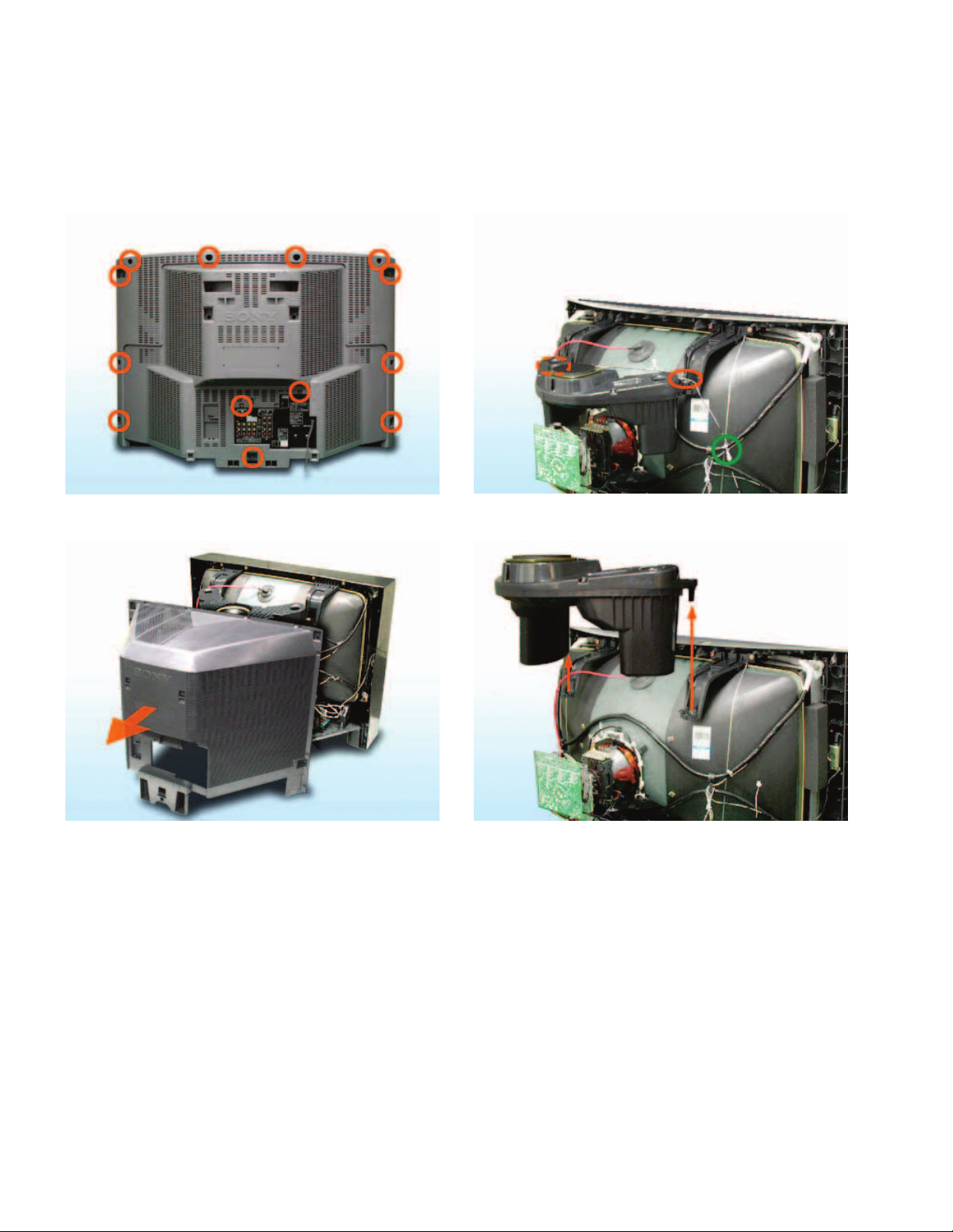
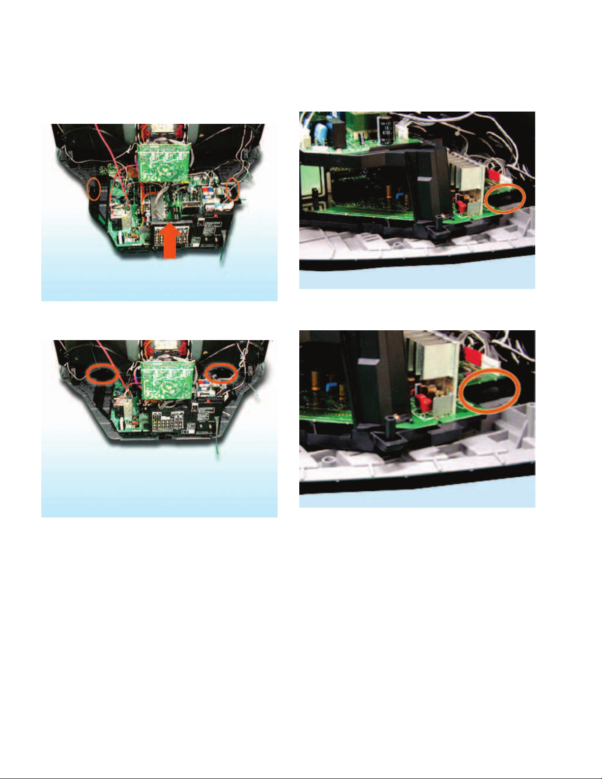
2-1. REAR COVER
1) Remove thirteen screws secured the rear cover.
2) Remove the rear cover by pulling backward.
2-2. SPEAKER BLOCK
1) Remove two screws secured the speaker and connector.
2) Remove the speaker upward.
– 8 –
2-3. CHASSIS ASSEMBLY
1) Remove two claws on both sides of the chassis assembly
by pulling up.
KV-DX32K9H/DX32K9H/B/DX32K90B/DX32K90L
RM-1006 RM-1006 RM-1006 RM-1006
2) Pull out the chassis assembly backward
– 9 –
KV-DX32K9H/DX32K9H/B/DX32K90B/DX32K90L
RM-1006 RM-1006 RM-1006 RM-1006
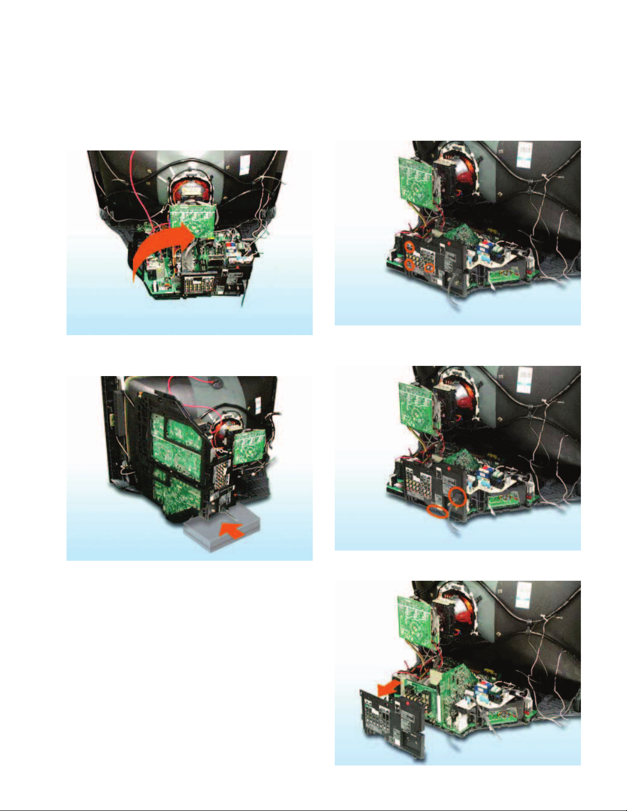
2-4. ASSEMBLING CHASSIS ASSEMBLY
1) Hold the both sides of the chassis assembly.
Enlarged view (Mid)
2) Push forward until the claws on both sides of the chassis
assembly fit into the beznet assembly.
Enlarged view (Full)
– 10 –
KV-DX32K9H/DX32K9H/B/DX32K90B/DX32K90L
RM-1006 RM-1006 RM-1006 RM-1006
2-5. SERVICE POSITION
1) Hold the chassis assembly in the rear.
2) Turn it clockwise 90 degrees and stand it.
3) Settle it by inserting the chassis assembly holder under
the U bracket.
2-6. U BRACKET
1) Remove three screws secured the U bracket.
2) Pull out the power cord and while pulling up the claw
secured the U bracket,
3) Remove the U bracket.
– 11 –
KV-DX32K9H/DX32K9H/B/DX32K90B/DX32K90L
RM-1006 RM-1006 RM-1006 RM-1006
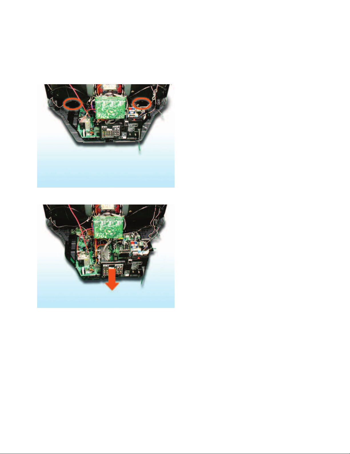
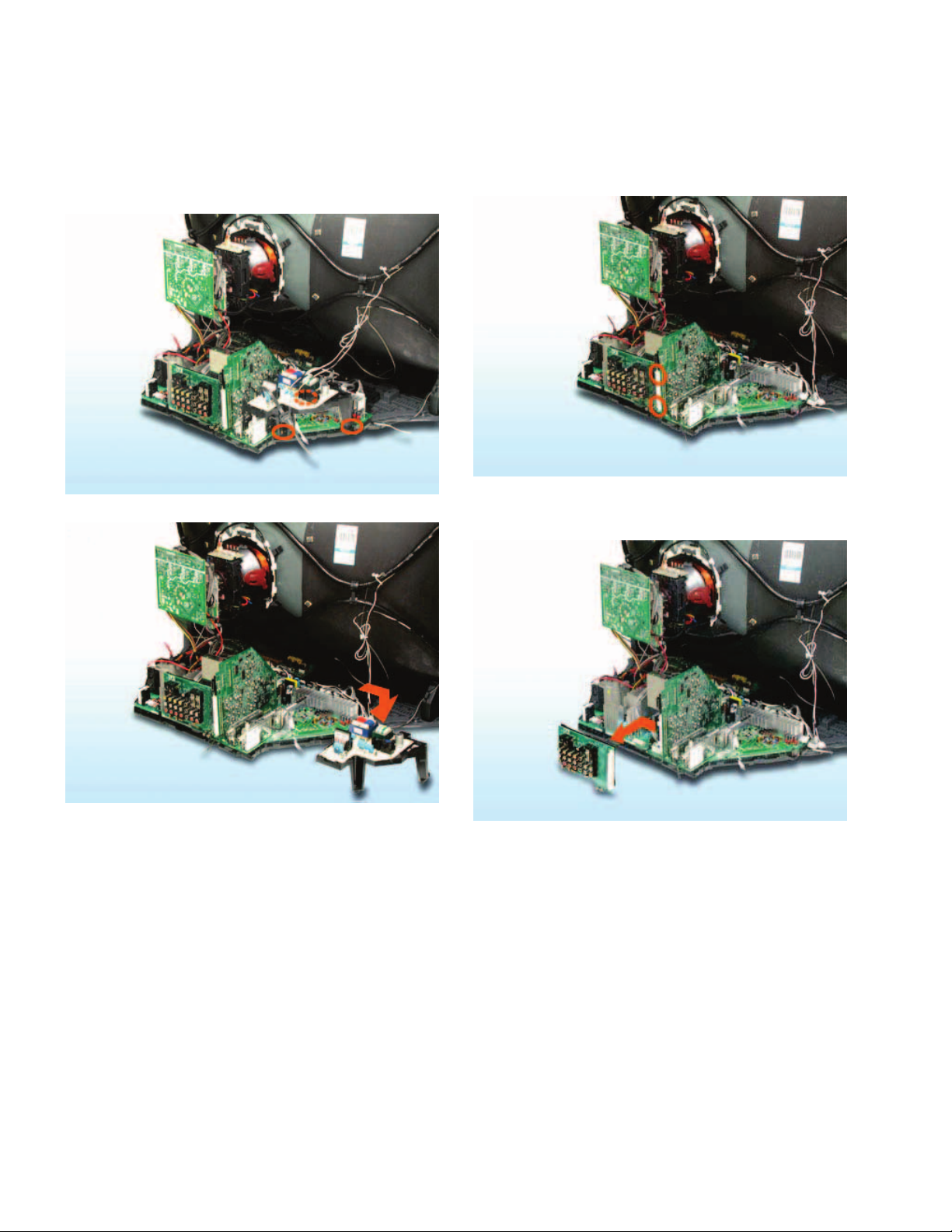
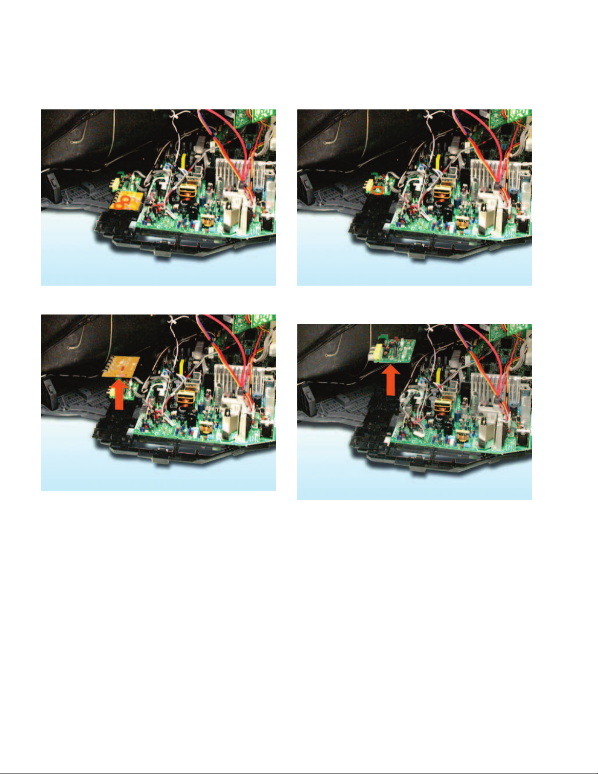
2-7. F4 BOARD
1) Remove three screws secured the F1 bracket.
2) Remove F4 board with the F1 bracket.
2-8. U3 BOARD
1) While pulling two claws on the B-to-B connector,
2) Remove U3 board from B1 board.
– 12 –
KV-DX32K9H/DX32K9H/B/DX32K90B/DX32K90L
RM-1006 RM-1006 RM-1006 RM-1006
2-9. B1 BOARD
1) Remove connector CN3003 on B1 board.
2) Remove B1 board while putting off three claws on two Bto-B connectors.
2-10. H1 BOARD
1) Remove two screws secured H1 board.
2) Remove H1 board.
– 13 –
KV-DX32K9H/DX32K9H/B/DX32K90B/DX32K90L
RM-1006 RM-1006 RM-1006 RM-1006
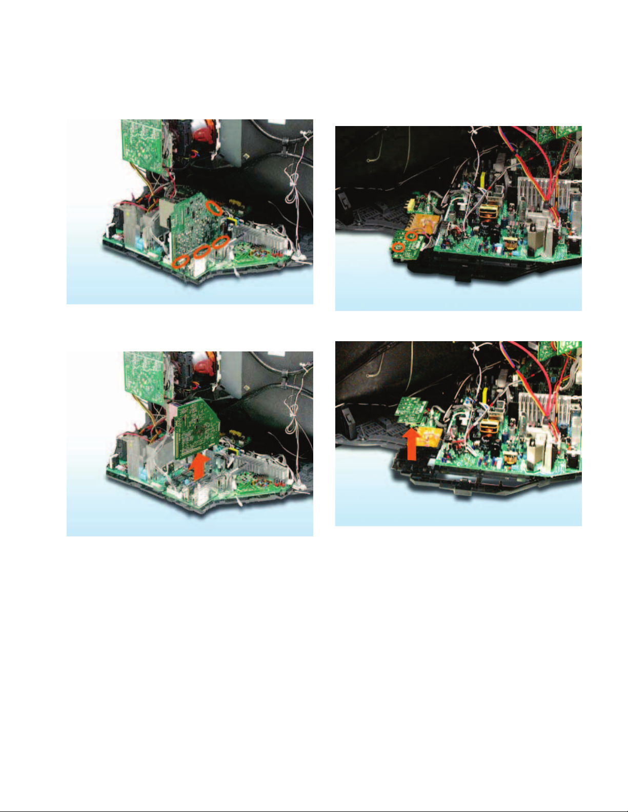
2-11. H2 BOARD
1) Remove two screws.
2) Remove H2 board.
2-12. H4 BOARD
1) Remove a screw.
2) Remove H4 board.
– 14 –
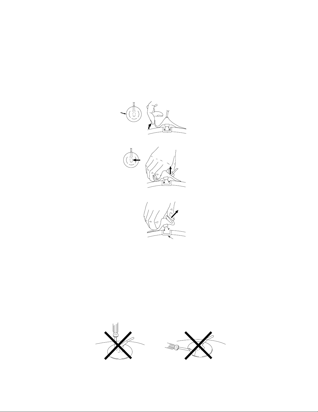
2-13. REMOVAL OF ANODE-CAP
KV-DX32K9H/DX32K9H/B/DX32K90B/DX32K90L
RM-1006 RM-1006 RM-1006 RM-1006
NOTE : After removing the anode, short circuit
the anode cap to the metal chassis, CRT shield or carbon paint on the
CRT.
• REMOVING
1 Turn up one side of the rubber
2 Using a thumb pull up the rubber
PROCEDURES
a
a
cap in the
b
cap firmly in the direction
direction indicated
the anode of the picture tube and
by the arrow a.
b
indicated by the arrow b.
c
3 When one side of the rubber
can be removed by turning up the rubber cap and pulling it up in the direction of the
arrow
c.
cap is separated
from the anode b
utton, the anode-cap
• HOW TO HANDLE AN ANODE-CAP
1 Do not dama
2 Do not press
A metal fitting called
3 Do not turn
The shatter-hook
ge the surface
the rubber too hard
the foot of rubber over too hard.
terminal will stick out
of anode-caps with
so as not to damage the inside of
the shatter-hook terminal is built into
or damage the rubber
sharp shaped objects.
anode-cap.
the rubber.
.
– 15 –
KV-DX32K9H/DX32K9H/B/DX32K90B/DX32K90L
RM-1006 RM-1006 RM-1006 RM-1006
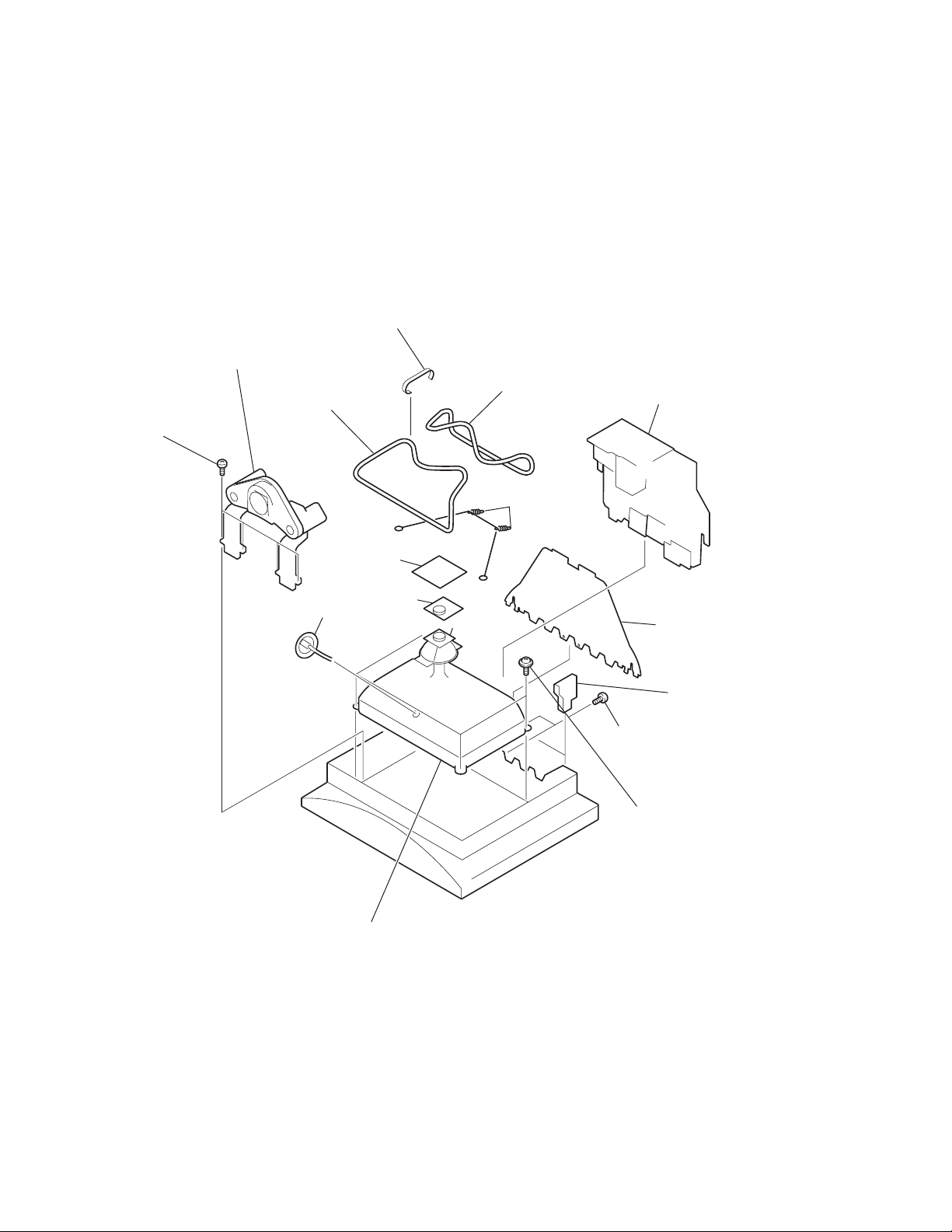
2-14. CRT
NOTE: After removing the anode, short circuit the anode of the picture tube
and the anode cap to the metal chassis, CRT shield or carbon paint
on the CRT.
1 Rear cover assembly
qs Binding band
3 Speaker box assembly
2 Screws
(+P 4x16)
qd Degauss coil
6 C3 board
7 Neck assembly
4 Anode cap
qd Degauss coil
qf Extension
springs
8 Deflection
yoke
5 Chassis assembly
0 Bottom cover
qa CRT supporter
9 Screws (+BVTP 4x8)
qg Screws
(Crown washer +TP 7x40)
qh CRT
– 16 –
2-15. PARTS LOCATION AND WIRING
KV-DX32K9H/DX32K9H/B/DX32K90B/DX32K90L
RM-1006 RM-1006 RM-1006 RM-1006
– 17 –
KV-DX32K9H/DX32K9H/B/DX32K90B/DX32K90L
RM-1006 RM-1006 RM-1006 RM-1006
SECTION 3
SERVICE MODE
3-1. METHOD OF SETTING THE SERVICE ADJUSTMENT
MODE
SERVICE MODE PROCEDURE
1. Standby mode. (Power off)
2. n 5 n (+) n
on the Remote Commander.
(Press each button within a second.)
3-2. SERVICE MODE ADJUSTMENT
Item NO.(register name)
Category
Data
7. If you want to recover the latest values press 0 then to
read the memory.
8. Press [MUTING] then to write into memory.
9. Turn power off.
Note: Press 8 then on the Remote Commander to initialize
or turn set off and on to exit.
3-3. MEMORY WRITE CONFIRMATION METHOD
1. After adjustment, turn power off with the remote commander.
2. Turn power on and set to Service Mode.
3. Call the adjusted items again and confirm they were adjusted.
3-4. ADJUSTING BUTTONS AND INDICATOR
3D-COMB
0 NRMD
FH: - - - - - /
FV: - - - - -
0 - - -
000
0
0
3. The SCREEN displays the item being adjusted.
4. Press 1 or 4 on the Remote Commander to select the
adjustment item.
5. Press 3 or 6 on the Remote Commander to change the data.
6. Press 2 or 5 on the Remote Commander to select the
category.
Every time you press 2(Category up), Service mode changes
in the order as shown below.
3D-COMB
2103-1
2150P-1
2150D-3
2151
D-CONV
MIDXE3
OSD
SNNR
Adjustment item up
Adjustment item down
(+)
Category up
Data up
Data down
Category down
2150P-2
2150P-3
2150P-4
2150D-1
2150D-2
2026
AP
AUTO-WIDE
MIDXE1
MIDXE2
TP
OP
RM-1006
– 18 –
KV-DX32K9H/DX32K9H/B/DX32K90B/DX32K90L
3D COMB
No. Name Standards
1 YAPS *1 Y-output correction
2 CLKS *1 System clock setting
3
4
5
6 CDL *1 C-signal phase with respect to the Y-signal
7 DYCO *2 DY detection coring level (Y detection coring)
8 DYGA *2 DY detection gain (Y motion detection gain)
9 DCCO *2 DC detection coring level (C motion detection coring)
10 DCGA *2 DC detection gain ( C motion detection gain)
11 YNRL *1 Frame recursive YNR nonlinear filter limit level
12 CNRL *1 Frame recursive CNR nonlinear filter limit level
13 VTRH *3 Hysteresis for Hsysnc non-standard signal detection
14 VTRR *3 Sensitivity for Hsysnc non-standard signal detection
15 LDSR *3 Sensitivity for frame non-standard signal detection
16 VAPG *4 V-aperture compensation gain
17 VAPI *4 V-aperture compensation convergence point
18 YPFT *5 Y peaking filter (BPF) center frequency
19 YPFG *5 Y peaking filter (BPF) gain
20 YHCO *1 Y output high frequency component coring
21 YHCG *1 Y output high frequency component coring gain
22 HSSL *1 Hsync slice level
23 VSSL *1 Vsync slice level
24 ADCL *1 ADC clock delay
25 D2GA *2 Moving detection gain
26 KILR *1 Killer detection reference
27 OP *1 Option: Selection of comb filter&recursive n.reduction types.
28 NR1 *6 Noise reduction on/off
29 NR2 *1 SNNR control on/off
31 HPLL *1 H-PLL filter
32 BPLL *1 Burst PLL filter
33 FSCF *1 Burst extraction gain
34 PLLF *1 PLL loop gain
35 CC3N *3 Selection if a line-comb filter C separation filter characteristic
36 HDP *1 Fine adjustment of the system H-phase
37 BGPS *1 Internal
38 BGPW *1
39 TEST *1 Test bit (0:Normal mode 1:Test mode) * forbidden setting
40 WSC *1 Amount of noise detection coring
41 LIND *3 DRC-M line-doubling setting for non-standard signals UHF/VHF&Video1-4
42 PFGO — (YPFG offset at GR on) * Not used
43 WSS *1
Remarks
RM-1006 RM-1006 RM-1006 RM-1006
3-5.SERVICE MODE LIST
– 19 –
KV-DX32K9H/DX32K9H/B/DX32K90B/DX32K90L
Standards *1
U/V VIDEO1 VIDEO2 VIDEO3
1 YAPS 3 3 3 3
2 CLKS 2 1
6 CDL 2 3
11 YNRL 1 1
12 CNRL 1 1
20 YHCO 0 0
21 YHCG 0 0
22 HSSL 12 12 12 12
23 VSSL 8 8
24 ADCL 1 1
26 KILR 3 3
27 OP 1
29 NR2 0 0 0 0
31 HPLL 1 1
32 BPLL 1 1
33 FSCF 0 0
34 PLLF 1 1
36 HDP 5 5 5 5
37 BGPS 4 4
38 BGPW 10 10 10 10
39 TEST 0 0
40 WSC 1 1 1 1
43 WSS 0 0 0 0
No. Name
Standards
33
33
11
11
11
11
11
111
11
11
00
00
88
00
00
44
VIDEO4/DEC S VIDEO1 S VIDEO2 S VIDEO3
1 YAPS 3 3 3 3
2 CLKS
6 CDL
11 YNRL
12 CNRL
20 YHCO
21 YHCG
22 HSSL 12 12 12 12
23 VSSL
24 ADCL
26 KILR
27 OP
29 NR2 0 0 0 0
31 HPLL
32 BPLL
33 FSCF
34 PLLF
36 HDP 5 5 5 5
37 BGPS
38 BGPW 10 10 10 10
39 TEST
40 WSC 1 1 1 1
43 WSS 0 0 0 0
No. Name
Standards
33 3 3
33 3 3
11 1 1
11 1 1
11 1 1
11 1 1
11 1 1
11 1 1
11 1 1
11 1 1
00 0 0
00 0 0
88 8 8
00 0 0
00 0 0
44 4 4
RM-1006 RM-1006 RM-1006 RM-1006
– 20 –
KV-DX32K9H/DX32K9H/B/DX32K90B/DX32K90L
Standards *2
3DYC 2DYC+YCNR MNNR YCNR
NRMD = 0 NRMD = 1 NRMD = 2 NRMD = 3
7 DYCO 2 2
8 DYGA 10 10
9 DCCO 5 5
10 DCGA 5 5
25 D2GA 4 4
Standards *3
UV/BS Video D component
13 VTRH 1 1 1
14 VTRR 1 1 1
15 LDSR 2 2 2
35 CC3N 0 0 0
41 LIND 0 0 0
Standards *4
Dynamic Standard Living
16 VAPG 7 0 0
17 VAPI 1 4 4
Standards *5
Dynamic Standard Living
AV Pro VM: Off AV Pro VM: Low,Mid,High
18 YPFT 3 3 3 3 3
19 YPFG 8 8 8 8 8
Dynamic Standard Living
AV Pro VM: Off AV Pro VM: Low,Mid,High
18 YPFT 3 3 3 3 3
19 YPFG 8 8 8 8 8
Standards *6
UV Video 1 S Video 1 Video 2
28 NR1 0 0 0 0
S Video2 Video 3 S Video 3 Video 4/DEC
28 NR1 0 0 0 0
No. Name Video
Standards
Standards
No.
No. Name
Standards
No. Name
Name
Name UV
Name
Standards
Standards
Standards
Standards
No. Name
No.
No.
VM: Off VM: Low VM: Mid VM: High
16 VAPG
17 VAPI
No. Name
Standards
AV Pro
0007
4441
RM-1006 RM-1006 RM-1006 RM-1006
– 21 –
KV-DX32K9H/DX32K9H/B/DX32K90B/DX32K90L
CXA2103 1
No. Name Standards
0 YLEV *1 Y-Out gain
1 CLEV *1 Cb&Cr-Out gain
2 SCON *2 Sub contrast
3 SCOL *2 Sub color
4 SHUE *2 Sub hue
5 YDLY *2 Y/C delay time
6 SHAP *3 Sharpness
7 SHF0 *3 Sharpness f0 selector
8 PREO *3 Sharpness pre/over-shoot ratio
9 BPF0 *3 Chroma band filter f0 setting
10 BPFQ *3 Chroma band filter Q setting
11 BPSW *3 Chroma bnad filter on/off
12 TRAP *3 Y block chroma trap filter on/off
13 LPF *3 Y Cb Cr-Output LPF on/off
14 AFCG *4 AFC Loop gain (PLL between Hsync & HVCO)
15 CDMD *4 V countdown system mode selector
16 SSMD *4 H&Vsync slide level setting
17 HMSK *4 Masking of macrovision signal on/off
18 HALI *4 H automatic adjustment on/off
19 PPHA *4 H TIM phase adjustment video
20 CBOF *1
21 CROF *1
22 ATPD 0 Auto-pedestal Inflection Point P&P & Favorite UBLK=0
23 DCTR 0 DC Transmission Ratio P&P & Favorite UBLK=0
24 RSCO *5
25 RSCL *5
26 RSHU *5
Standards *1
UV/Video D1,D2
0 YLEV 29 26
1 CLEV 22 39
20 CBOF 41 41
21 CROF 37 41
Standards *2
UV Video
2 SCON 6 7
3 SCOL 7 6
4 SHUE 7 9
5 YDLY 0 0
No. Name
No. Name DRC
Standards
Remarks
Standards
RM-1006 RM-1006 RM-1006 RM-1006
– 22 –
KV-DX32K9H/DX32K9H/B/DX32K90B/DX32K90L
Standards *3
UV GR: Off
Video D1,D2 S Video
6 SHAP
7 SHF0
8 PREO
9 BPF0
10 BPFQ
11 BPSW
12 TRAP
13 LPF
Standards *4
UV Video D1,D2
14 AFCG
15 CDMD
16 SSMD
17 HMSK
18 HALI
19 PPHA
Standards *5
Standards
GR: On
24 RSCO 3
25 RSCL 3
26 RSHU 4
No. Name
No. Name
No. Name
Standards
Standards
000
10 0
33 3
00 0
11 1
00 0
79 0
0
000 0
000 0
300 0
330 0
333 3
10 55
100 0
RM-1006 RM-1006 RM-1006 RM-1006
– 23 –
KV-DX32K9H/DX32K9H/B/DX32K90B/DX32K90L
CXA2150P-1
No. Name Standards
0 SBOT *1 Offset for SBRT
1 YOF *1 Y OFFSET: DC-offset for Y signal
2 CBOF *1 CB OFFSET: DC-offset for Cb signal
3 CROF *1 CR OFFSET: DC-offset for Cr signal
4 RDVL 41
5 GDVL 33
6 BDVL 28
7 RCTL 51
8 GCTL 34
9 BCTL 48
10 BRTL 24
11 RDVH 41
12 GDVH 32
13 BDVH 30
14 RCTH 51
15 GCTH 37
16 BCTH 47
17 BRTH 26
18 WBSW -
19 SBOF *2 Offset for SBRT
20 RDOF *2 Offset for RDRV
21 GDOF *2 Offset for GDRV
22 BDOF *2 Offset for BDRV
23 RCOF *2 Offset for RCUT
24 GCOF *2 Offset for GCUT
25 BCOF *2 Offset for BCUT
26 GMLW 0
27 GMHI 2
Standards *1
D480P
D720P/1035i/1080i D1035i/1080i D480i
AVM-YUV720P/1080i AVM-YUV1080i
MID ANALOG
)
0 SBOT 7 7 7 7 7
1 YOF 10 0 0 0 0
2 CBOF 31 47 43 36 31
3 CROF 31 43 41 36 31
Standards *2
Color temp.: Mid Color temp.: Low
19 SBOF 64 64
20 RDOF 63 63
21 GDOF 65 67
22 BDOF 64 74
23 RCOF 63 63
24 GCOF 62 66
25 BCOF 55 73
Remarks
UV/Video
AVM-YUV480P
Standards
Standards
AVM-RGB,YUV480i
No. Name
No. Name
RM-1006 RM-1006 RM-1006 RM-1006
– 24 –
KV-DX32K9H/DX32K9H/B/DX32K90B/DX32K90L
CXA2150P-2
No. Name Standards
0
1
2 BLKB 3 BLK BTM: RGB output bottom limit level (Black level)
3 LIML 0 PLIMIT LEV: Threshold level for excessively high inputs
4 PABL 15 P ABL: DC-level in RGB output detection for PEAK ABL
5 SABL 0 S ABL: S ABL gain
6 AGNG 0 AGING W/AGING B: AGING W/AGING B modes on/off
7 AKBO 0 AKBOFF: Automatic/Manual = Cut off setting
8 SYPH *1 SYNC PHASE: Hsync delay with respect to Video (100%H-period)
9 CLPH *1 CLP PHASE: Internal clamp pulse phase (100%H-period)
10 CLGA *1 CLP GATE: Switch for the gated internal clamp pulse with Hsync
11 0 JAXIS: color axis switch
12 0 BLKO: Blanking switch
Standards *1
D,AVM-YUV D,AVM-RGB,YUV D,AVM-RGB,YUV D,AVM-RGB,YUV
480i 480p 1035i/1080i 720p
8 SYPH 0 0 0 0 0
9 CLPH 3 3 3 3 3
10 CLGA 00000
Remarks
UV/Video
Standards
No. Name
CXA2150P-3
No. Name Standards
0 SYSM *1 SYSTEM: Signal bandwidth setting
1 UVML *1 VM LEV: VM OUT level
2 VMMO *1 System Micro pin#40
3 VMCR *1 VM COR: VM OUT coring level
4 VMLM *1 VM LMT: VM OUT limit level
5 VMF0 *1 VM F0: VM f0
6 VMDL *1 VM DLY:VM OUT phase (defined by phase difference from R OUT)
7 SHOF *1 Offset for USHP=SHOF x 4
8 SHF0 *1 SHP F0: Sharpness circuit f0
9 PROV *1 PRE/OVER: Y signal pre/over-shoot ratio
10 F1LV *1 SHP F1: Sharpness for higher f0 (4.2/5.6Mhz @NORMAL mode)
11 CDSP *1 SHP CD: Sharpness in part of high color saturation
12 LTLV *1 LTI LEV: Luminance transient improvement (LTI)
13 LTMD *1 LTI MODE: LTI mode setting
14 CTLV *1 CTI LEV: Chrominance transient improvement (CTI)
15 CTMD *1 CTI MODE: CTI mode setting
16 UBOF *1 Offset for UBRT (Picture clarity adjustment)
17 UCOF *1 Offset for UCOL=UCOF x 2 (Picutre clarity adjustment)
18 UHOF *1 Offset for UHUE (Picutre clarity adjustment)
19 MIDE *2 MID enhancement setting
20 VMOF 1
21 VDCG 1
22 POCG 1
23 LTOF 1
Remarks
RM-1006 RM-1006 RM-1006 RM-1006
– 25 –
KV-DX32K9H/DX32K9H/B/DX32K90B/DX32K90L
Standards *1
D,AVM-YUV D,AVM-RGB,YUV D,AVM-RGB,YUV D,AVM-RGB,YUV
1035i/1080i (ANALOG)480i 480p
480i 480p
720p
720p
0 SYSM
1 UVML
2 VMMO
3 VMCR
4 VMLM
5 VMF0
6 VMDL
7 SHOF
8 SHF0
9 PROV
10 F1LV
11 CDSP
12 LTLV
13 LTMD
14 CTLV
15 CTMD
16 UBOF
17 UCOF
18 UHOF
D,AVM-YUV D,AVM-RGB,YUV D,AVM-RGB,YUV D,AVM-RGB,YUV
1035i/1080i (ANALOG)
0 SYSM
1 UVML
2 VMMO
3 VMCR
4 VMLM
5 VMF0
6 VMDL
7 SHOF
8 SHF0
9 PROV
10 F1LV
11 CDSP
12 LTLV
13 LTMD
14 CTLV
15 CTMD
16 UBOF
17 UCOF
18 UHOF
Video
Standards
No. Name
Standards
AI Mode: Living
AI Mode: Dynamic
UV Video
UV
No. Name
1 11132
323233
000000
1 10000
333333
1 10101
0 22222
1 00030
1 11111
030223
0 03002
3 33333
223222
1 11111
3 10000
0 00000
7 777109
211000
111000
1 11132
223222
1 11111
1 10000
3 23333
1 11101
021222
000030
0 11111
0 00223
0 03302
333333
1 12111
1 11111
1 00003
000000
7 77777
211110
2 22200
RM-1006 RM-1006 RM-1006 RM-1006
– 26 –
KV-DX32K9H/DX32K9H/B/DX32K90B/DX32K90L
480i 480p
720p
480i 480p
720p
D,AVM-YUV
D
,
AVM-RGB, YUV
D,AVM-RGB,YUV D,AVM-RGB,YUV
1035i/1080i (ANALOG)
0 SYSM
1 UVML
2 VMMO
3 VMCR
4 VMLM
5 VMF0
6 VMDL
7 SHOF
8 SHF0
9 PROV
10 F1LV
11 CDSP
12 LTLV
13 LTMD
14 CTLV
15 CTMD
16 UBOF
17 UCOF
18 UHOF
UV Video
D,AVM-YUV
D,AVM-RGB,YUV
D,AVM-RGB,YUV D,AVM-RGB,YUV
1035i/1080i (ANALOG)
0 SYSM
1 UVML
2 VMMO
3 VMCR
4 VMLM
5 VMF0
6 VMDL
7 SHOF
8 SHF0
9 PROV
10 F1LV
11 CDSP
12 LTLV
13 LTMD
14 CTLV
15 CTMD
16 UBOF
17 UCOF
18 UHOF
Standards
AI Mode: AV Pro
Video
No. Name
No. Name
Standards
AI Mode: Standard
UV
1 11132
2 23232
0 00000
1 10000
3 33333
1 11101
0 21222
0 01000
0 11111
0 30233
0 03332
3 33333
1 13101
1 11111
2 00100
0 00000
7 77777
2 11210
2 22200
1 11132
0 00000
0 00000
1 10000
3 33333
1 11101
0 21222
0 00000
0 11111
0 30223
0 03300
0 30000
0 00000
1 11111
0 00000
0 00000
7 77777
0 00010
0 00000
RM-1006 RM-1006 RM-1006 RM-1006
– 27 –
KV-DX32K9H/DX32K9H/B/DX32K90B/DX32K90L
Standards *2
AVM-YUV AVM-RGB,YUV AVM-RGB,YUV AVM-RGB,YUV
480i 480P 1035i/1080i 720P
19 MIDE 3 7 23 11 11 27
AVM-YUV AVM-RGB,YUV AVM-RGB,YUV AVM-RGB,YUV
480i 480P 1035i/1080i 720P
19 MIDE 2 6 22 10 10 26
AVM-YUV AVM-RGB,YUV AVM-RGB,YUV AVM-RGB,YUV
480i 480P 1035i/1080i 720P
19 MIDE 1 5 21 9 9 25
AVM-YUV AVM-RGB,YUV AVM-RGB,YUV AVM-RGB,YUV
480i 480P 1035i/1080i 720P
19 MIDE 0 4 20 8 8 24
UV Video
UV
UV Video
AI Mode: Living
D Componemt
AI Mode: AV Pro
D Componemt
UV Video
No. Name
Standards
Standards
Standards
Standards
AI Mode: Dynamic
D Componemt
AI Mode: Standard
D Componemt
No. Name
Video
No. Name
No. Name
RM-1006 RM-1006 RM-1006 RM-1006
– 28 –
KV-DX32K9H/DX32K9H/B/DX32K90B/DX32K90L
CXA2150P-4
No. Name Standards
0 UPIC *1 PICTURE: Picture
1 UBRT *1 BRIGHT: Brightness
2 UCOL *1 COLOR:
3 UHUE *1 HUE:Hu
4 USHP *1 SHARPNESS: Sharpness
5 UTMP *1 Color Temperature (0:Warm 1:Neutral 2:Cool)
6 UDCL *1 DCOL: D
7 AXIS *2 COL AXIS: color matrix setting
8 UGAM *3 GAMMA/GAMMA L: RGB output GAMMA correction setting
9 AGAM *4 GAMMA/GAMMA L (AV Pro user control) - Void Data
10 GSBO *5 Offset for SBRT
11 GCOO *5 Offset for UCOL
12 GHUO *5 Offset for UHUE
13 UBLK *3 Item#15-18 pack F1 data controls
14 ABLK *6 (Av Pro user control) - Void Data
15 DCTR *7 DC TRAN: Y signal DC transmission
16 DPIC *7 DPIC LEV: Y signal AUTO PEDESTAL level
17 DSBO *7 Offset for SBRT
18 ABLM *7 ABL MODE: ABL mode
19 ABLT *8 ABL TH: ABL current detection Vth contro
20 ABLC *8
21 EPOF *9 Offset for UPIC=EPOF x (UPIC/63) (for power save) - Void Data
22 SPOF *10 Offset for UPIC=SPOF x (UPIC/64) - Data Not used
23 SCON *11 SUB CONTRAST: SUB PICTURE
24 CLOF *11 Offset for UCOL
25 HUOF *11 Offset for UHUE
26 USOF —
Standards *1
Dynamic Standard Living AV Pro
0 UPIC 53 473131
1 UBRT 26 31 31 31
2 UCOL 35 33 31 31
3 UHUE 31 31 31 31
4 USHP 31 31 31 31
5 UTMP 2 2 2 1
6 UDCL 3 2 2 0
Standards *2
UV/Video D, AVM-YUV D, AVM-RGB,YUV DD, AVM-RGB,YUV D, AVM-RGB,YUV
480i 480P 1035i 1080i
7 AXIS 3 3 3 333
UV/Video D, AVM-YUV D, AVM-RGB,YUV DD, AVM-RGB,YUV D, AVM-RGB,YUV
480i 480P 1035i 1080i 720p
720p
7 AXIS 3 3 3 333
Remarks
Standards
Standards
AI Mode: AV Pro
Standards
AI Mode: Dynamic, Standard, Living
No. Name
No.
No. Name
Name
RM-1006 RM-1006 RM-1006 RM-1006
– 29 –
 Loading...