

Sony KV-21FA350, KV-21FA550 Service Manual

HISTORY INFORMATION FOR THE FOLLOWING MANUAL:
SERVICE MANUAL
MODEL NAME REMOTE COMMANDER DESTINATION CHASSIS NO.
KV-21FA350
KV-21FA350
KV-21FA550
KV-21FA550
RM-YA005 LATIN NORTH SCC-S79K-A
RM-YA005 LATIN SOUTH SCC-S79L-A
RM-YA005 LATIN NORTH SCC-S79M-A
RM-YA005 LATIN SOUTH SCC-S79N-A
BX-1S
CHASSIS
ORIGINAL MANUAL ISSUE DATE: 2/2007
REVISION DATE SUBJECT
2/2007 No revisions or updates are applicable at this time.
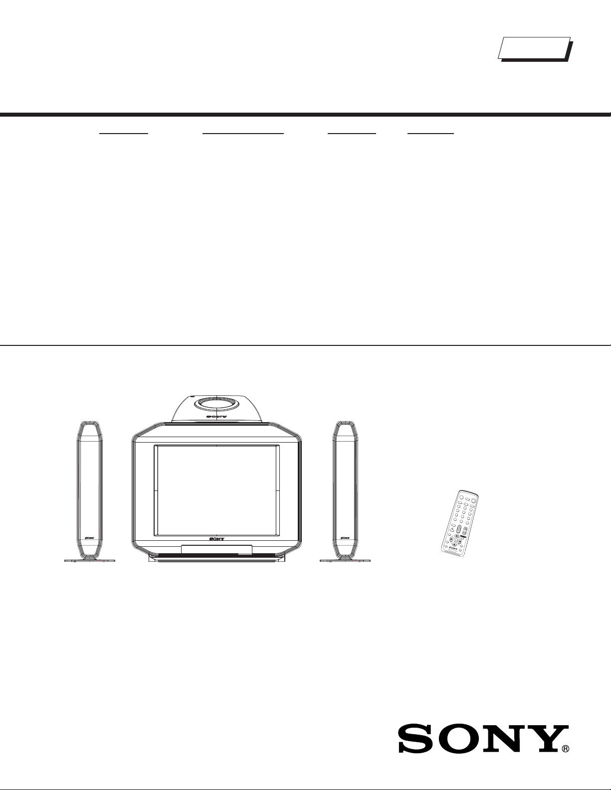
TRINITRON® COLOR TELEVISION
9-883-736-01
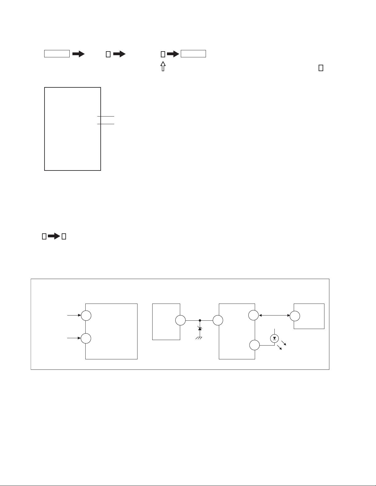
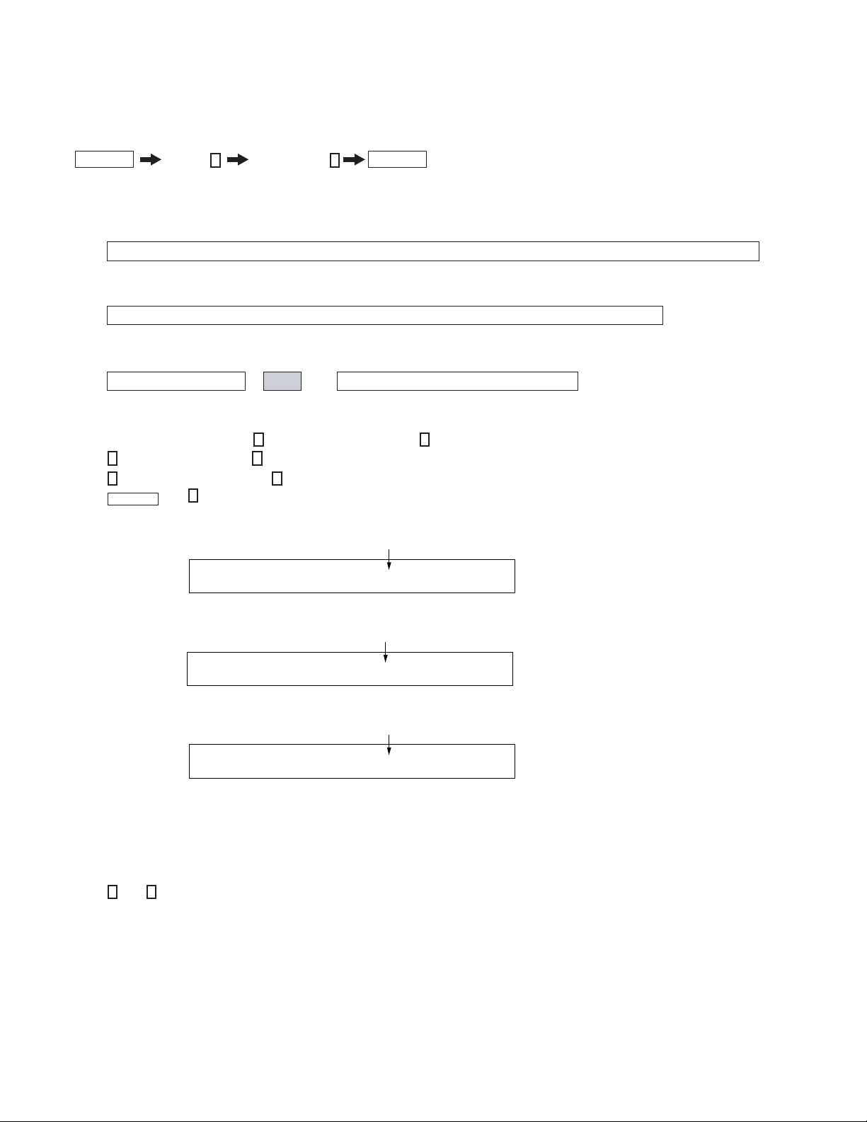
Self Diagnosis
+
TV
P
O
W
E
R
T
V
/
V
ID
E
O
C
H
R
E
T
U
R
N
S
O
U
N
D
M
O
D
E
S
L
E
E
P
1
6
:9
R
E
S
E
T
V
O
L
D
IS
P
L
A
Y
P
IC
T
U
R
E
M
O
D
E
M
T
S
/S
A
P
M
U
T
I
N
G
RM-Y
A005
1
2
3
4
6
7
8
9
0
5
EN
T
JU
M
P
W
EG
A G
A
TEWEGAGATE
C
C
Supported model
SERVICE MANUAL
MODEL NAME REMOTE COMMANDER DESTINATION CHASSIS NO.
KV-21FA350
KV-21FA350
KV-21FA550
KV-21FA550
RM-YA005 LATIN NORTH SCC-S79K-A
RM-YA005 LATIN SOUTH SCC-S79L-A
RM-YA005 LATIN NORTH SCC-S79M-A
RM-YA005 LATIN SOUTH SCC-S79N-A
BX-1S
CHASSIS
KV-21FA550 RM-YA005
TRINITRON® COLOR TELEVISION
9-883-736-01

KV-21FA350/21FA550
TABLE OF CONTENTS
SECTION TITLE PAGE
Specifi cations ....................................................................................................................................................................................................... 4
Warnings and Cautions ........................................................................................................................................................................................ 5
Safety Check-Out ................................................................................................................................................................................................. 6
Self-Diagnostic Function ...................................................................................................................................................................................... 7
SECTION 1: DISASSEMBLY ............................................................................................................................................................................................. 9
1-1. Rear Cover Removal .................................................................................................................................................................................... 9
1-2. Chassis Assembly Removal ......................................................................................................................................................................... 9
1-3. Service Position ............................................................................................................................................................................................ 9
1-4. Picture Tube Removal ................................................................................................................................................................................ 10
Anode Cap Removal Procedure ................................................................................................................................................................. 10
SECTION 2: SET-UP ADJUSTMENTS .............................................................................................................................................................................11
2-1. Beam Landing .............................................................................................................................................................................................11
2-2. Convergence .............................................................................................................................................................................................. 12
2-3. Focus .......................................................................................................................................................................................................... 13
2-4. Screen (G2) ................................................................................................................................................................................................ 14
SECTION 3: CIRCUIT ADJUSTMENTS .......................................................................................................................................................................... 15
3-1. Remote Adjustment Buttons and Indicators ............................................................................................................................................... 15
3-2. Accessing the Service Menu Mode ............................................................................................................................................................ 16
3-3. Confi rming Service Adjustment Changes ................................................................................................................................................... 17
3-4. White Balance Adjustments ........................................................................................................................................................................ 17
3-5. Picture Quality Adjustments ....................................................................................................................................................................... 17
3-6. Service Data ............................................................................................................................................................................................... 19
SECTION 4: DIAGRAMS ................................................................................................................................................................................................. 28
4-1. Circuit Boards Location .............................................................................................................................................................................. 28
4-2. Printed Wiring Board and Schematic Diagram Information ........................................................................................................................ 28
4-3. Block Diagram ............................................................................................................................................................................................ 29
Signal Flow Block Diagram ........................................................................................................................................................................ 29
4-4. Schematics and Supporting Information .................................................................................................................................................... 30
A Board Schematic Diagram (1 of 6) ......................................................................................................................................................... 30
A Board Schematic Diagram (2 of 6) ......................................................................................................................................................... 31
A Board Schematic Diagram (3 of 6) ......................................................................................................................................................... 32
A Board Schematic Diagram (4 of 6) ......................................................................................................................................................... 33
A Board Schematic Diagram (5 of 6) ......................................................................................................................................................... 34
A Board Schematic Diagram (6 of 6) ......................................................................................................................................................... 35
CV Board Schematic Diagram ................................................................................................................................................................... 37
H2 Board Schematic Diagram ................................................................................................................................................................... 38
J4 Board Schematic Diagram .................................................................................................................................................................... 39
W Board Schematic Diagram ..................................................................................................................................................................... 40
4-5. Semiconductors .......................................................................................................................................................................................... 41
SECTION 5: EXPLODED VIEWS .................................................................................................................................................................................... 42
5-1. Chassis and Speakers ............................................................................................................................................................................... 42
5-2. Picture Tube ............................................................................................................................................................................................... 43
SECTION 6: ELECTRICAL PARTS LIST ........................................................................................................................................................................ 44
KV-21FA350/21FA550
3
SPECIFICATIONS
KV-21FA350/21FA550
Television system
American TV standard, NTSC
Channel coverage
VHF: 2-13/UHF: 14-69/CATV: 1-125
Antenna
75-ohm external antenna terminal for VHF/UHF
Picture tube
FD Trinitron® tube
Visible screen size
508mm (20-inch) picture measured diagonally
Actual screen size
533.4mm (21-inch) measured diagonally
Supplied Accessories
Remote Commander RM-YA005
Two Size AA (R6) Batteries
Converter EAC-25
Dipolo Antenna
2 - Bocinas Satelite cables (KV-21FA550 Only)
KV-21FA350/21FA550
1)
1 Vp-p 75 ohms unbalanced, sync negative
2) Y: 1Vp-p 75 ohms unbalanced, sync negative
C: 0.286 Vp-p (Burst signal), 75 ohms
3) Y: 1.0 Vp-p, 75 ohms, sync negative; PB: 0.7 Vp-p, 75 ohms;
PR Vp-p, 75 ohms.
4)
500 mVrms (100% modulation), Impedance: 47 kilohms
5)
This specifi cation is the maximum wattage.
Trademarks and Copyrights
As an ENERGY STAR® Partner, Sony
Corporation has determined that this
product meets the ENERGY STAR®
guidelines for energy efficiency. ENERGY
STAR® is a U.S. regis tered mark.
TruSurround, SRS and the ( )® symbol are trademarks of
SRS Labs, Inc.
Manufactured under license from BBE Sound,
Inc. Licensed by BBE Sound, Inc. under USP
4638258, 5510752 a nd 5736897. BBE and BBE
symbol are registered trademarks of BBE
Sound, Inc.
Sony, FD Trinitron, WEGA®, Steady Sound and Intelligent Picture
are
registered trademarks of Sony Corporation.
Design and specifi cations are subject to change without notice.
4

KV-21FA350/21FA550
WARNINGS AND CAUTIONS
CAUTION
Short circuit the anode of the picture tube and the anode cap to the metal chassis, CRT shield, or carbon painted on the CRT, after
removing the anode.
WARNING!!
An isolation transformer should be used during any service to avoid possible shock hazard, because of live chassis. The chassis of this
receiver is directly connected to the AC power line.
! SAFETY-RELATED COMPONENT WARNING!!
Components identifi ed by shading and ! mark on the schematic diagrams, exploded views, and in the parts list are critical for safe
operation. Replace these components with Sony parts whose part numbers appear as shown in this manual or in supplements published
by Sony. Circuit adjustments that are critical for safe operation are identifi ed in this manual. Follow these procedures whenever critical
components are replaced or improper operation is suspected.
KV-21FA350/21FA550
5
SAFETY CHECK-OUT
KV-21FA350/21FA550
After correcting the original service problem, perform the following
safety checks before releasing the set to the customer:
1. Check the area of your repair for unsoldered or poorly soldered
connections. Check the entire board surface for solder splashes and
bridges.
2. Check the interboard wiring to ensure that no wires are “pinched” or
touching high-wattage resistors.
3. Check that all control knobs, shields, covers, ground straps, and
mounting hardware have been replaced. Be absolutely certain that
you have replaced all the insulators.
4. Look for unauthorized replacement parts, particularly transistors,
that were installed during a previous repair. Point them out to the
customer and recommend their replacement.
5. Look for parts which, though functioning, show obvious signs of
deterioration. Point them out to the customer and recommend their
replacement.
6. Check the line cords for cracks and abrasion. Recommend the
replacement of any such line cord to the customer.
7. Check the B+ and HV to see if they are specifi ed values. Make sure
your instruments are accurate; be suspicious of your HV meter if
sets always have low HV.
8. Check the antenna terminals, metal trim, “metallized” knobs,
screws, and all other exposed metal parts for AC leakage. Check
leakage as described below.
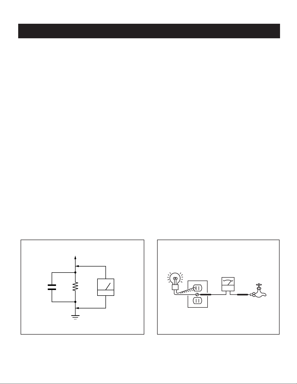
Leakage Test
The AC leakage from any exposed metal part to earth ground and from
all exposed metal parts to any exposed metal part having a return to
chassis, must not exceed 0.5 mA (500 microamperes). Leakage current
can be measured by any one of three methods.
1. A commercial leakage tester, such as the Simpson 229 or RCA
WT-540A. Follow the manufacturers’ instructions to use these
instructions.
2. A battery-operated AC milliampmeter. The Data Precision 245
digital multimeter is suitable for this job.
3. Measuring the voltage drop across a resistor by means of a VOM
or battery-operated AC voltmeter. The “limit” indication is 0.75 V,
so analog meters must have an accurate low voltage scale. The
Simpson’s 250 and Sanwa SH-63TRD are examples of passive
VOMs that are suitable. Nearly all battery-operated digital
multimeters that have a 2 VAC range are suitable (see Figure A).
How to Find a Good Earth Ground
A cold-water pipe is a guaranteed earth ground; the cover-plate
retaining screw on most AC outlet boxes is also at earth ground. If the
retaining screw is to be used as your earth ground, verify that it is at
ground by measuring the resistance between it and a cold-water pipe
with an ohmmeter. The reading should be zero ohms.
If a cold-water pipe is not accessible, connect a 60- to 100-watt troublelight (not a neon lamp) between the hot side of the receptacle and the
retaining screw. Try both slots, if necessary, to locate the hot side on
the line; the lamp should light at normal brilliance if the screw is at
ground potential (see Figure B).
0.15 µF
Figure A. Using an AC voltmeter to check AC leakage. Figure B. Checking for earth ground.
KV-21FA350/21FA550
To Exposed Metal
Parts on Set
1.5 K Ω
Earth Ground
AC
Voltmeter
(0.75 V)
Trouble Light
AC Outlet Box
Ohmmeter
Cold-water Pipe
6
KV-21FA350/21FA550
SELF-DIAGNOSTIC FUNCTION
Self Diagnosis
Supported model
The units in this manual contain a self-diagnostic function. If an error occurs, the STANDBY LED indicator will automatically begin to fl ash. The number of
times the LED fl ashes translates to a probable source of the problem. A defi nition of the STANDBY LED fl ash indicators is listed in the instruction manual
for the user’s knowledge and reference. If an error symptom cannot be reproduced, the Remote Commander can be used to review the failure occurrence
data stored in memory to reveal past problems and how often these problems occur.
1. Diagnostic Test Indicators
When an error occurs, the STANDBY LED indicator will fl ash a set number of times to indicate the possible cause of the problem. If there is more than
one error, the indicator will identify the fi rst of the problem areas.
Results for all of the following diagnostic items are displayed on screen. No error has occurred if the screen displays a “0”.
Diagnostic Item
Description
Power does not turn on
+B overcurrent (OCP)*
V-Protect (OVP)
IK (AKB)
Power Supply
NG (+5V) for
Video Processor
No. of Times
STANDBY LED
Indicator Flashes
Does not light
2 times *
4 times
5 times
8 times
Self-Diagnositc
Display/
Diagnostic Result
2:0
or
2:1 - 255
4:0
or
4:1 - 255
5:0
or
5:1 - 255
8:0
or
8:1 - 255
Probable Cause Location
• Power cord is not plugged in.
• Fuse is burned out (F600). (A Board)
• H.OUT (Q805) is shorted. (A Board)
• IC751 is shorted. (C Board)
• +13V is not supplied. (A Board)
• IC804 is faulty. (A Board)
• Video OUT (IC1545) is faulty(A Board)
• IC001 is faulty. (A Board)
• Screen (G2) is improperly adjusted.**
• IC604 is faulty.
• IC602 is faulty.
Detected Symptoms
• Power does not come on.
• No power is supplied to the TV.
• AC Power supply is faulty.
• Power does not come on.
• Load on power line is shorted.
• Has entered standby state after horizontal raster.
• Vertical defl ection pulse is stopped.
• Power line is shorted or power supply is stopped.
• No raster is generated.
• CRT Cathode current detection reference pulse
output is small.
• No power supply to CRT Anode.
• No RASTER is generated.
*One fl ash count is not used for self-diagnostic.
*If a +B overcurrent is detected, stoppage of the vertical defl ection is detected simultaneously. The symptom that is diagnosed fi rst by the mircrocontroller
is displayed on the screen.
**Refer to Screen (G2) Adjustments in Section 2-4. of this manual.
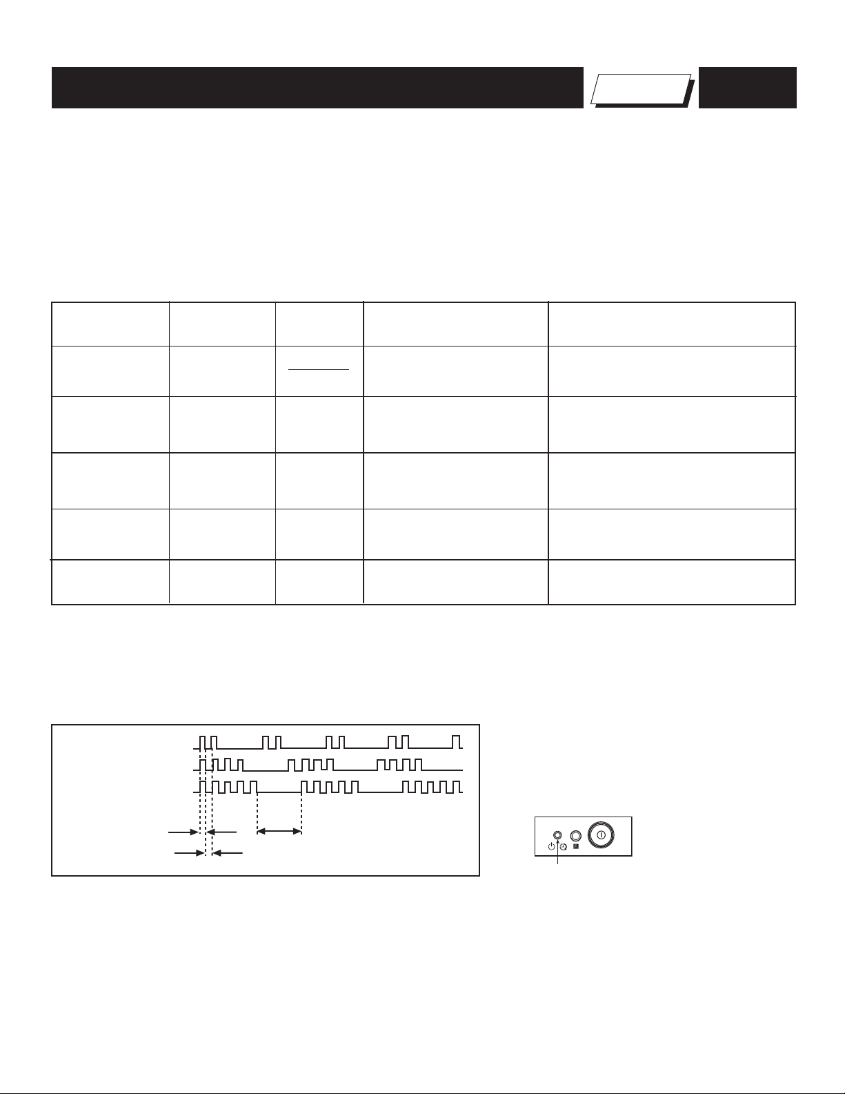
2. Display of STANDBY LED Flash Count
2 times
4 times
5 times
LED ON 0.3 sec.
LED OFF 0.3 sec.
LED OFF
3 sec.
Standby indicator
3. Stopping the STANDBY LED Indicator Flash
Turn off the power switch on the TV main unit or unplug the power cord from the outlet to stop the STANDBY LED Indicator from fl ashing.
4. Self-Diagnostic Screen Display
For errors with symptoms such as “power sometimes shuts off” or “screen sometimes goes out” that cannot be confi rmed, it is possible to bring up past
occurrences of failure on the screen for confi rmation.
KV-21FA350/21FA550
7
To Bring Up Screen Test
In standby mode, press buttons on the Remote Commander sequentially, in rapid succession, as shown below:
KV-21FA350/21FA550
The following screen will be displayed indicating the error count:
Handling of Self-Diagnostic Screen Display
Since the diagnostic results displayed on the screen are not automatically cleared, always check the self-diagnostic screen during repairs. When you
have completed the repairs, clear the result display to “0”.
Unless the result display is cleared to “0”, the self-diagnostic function will not be able to detect subsequent faults after completion of the repairs.
Clearing the Result Display
To clear the result display to “0”, press buttons on the Remote Commander sequentially when the diagnostic screen is displayed, as shown below:
DISPLAY
SELF DIAGNOSTIC
2 OCP : 0
3 OVP : N/A
4 VSTOP : 0
5 AKB : 1
8 SUP : 0
101 WDT : N/A
SERIAL:
MODEL:
Channel
5
Sound Volume -
Number “0” means that no fault was detected.
Number “1” means a fault was detected one time only.
POWER
Note that this differs from entering the Service Mode (Sound Volume + ).
Channel 8
Quitting the Self-Diagnostic Screen
To quit the entire self-diagnostic screen, turn off the power switch on the Remote Commander or the main unit.
Self-Diagnostic Circuit
FROM
C BOARD
IC751 PIN 5
0
A BOARD
IC001
Y/CHROMA JUNGLE
84
IK
A BOARD
IC804
V. OUT
F.B-PLS
3
A BOARD
IC001
SYSTEM
13
V. GUARD
SDAO
109
A BOARD
IC003
MEMORY
5
SDA
FROM
32
A BOARD
Q816
COLLECTOR
+B overcurrent (OCP)
Occurs when an overcurrent on the +B (135V) line is detected by pin 32 of IC001 (A Board). If the voltage of pin 32 of IC001 (A Board) is more than 4V
when V.SYNC is more than seven verticals in a period, the unit will automatically turn off.
V-Protect
Occurs when an absence of the vertical defl ection pulse is detected by pin 13 of IC001 (a Board). Power supply will shut down when waveform interval
exceeds 2 seconds.
IK (AKB)
If the RGB levels* do not balance within 15 seconds after the power is turned on, this error will be detected by IC001 (A Board). TV will stay on, but there
will be no picture.
Power Supply NG (+5V) for Video Processor
Occurs when IC001 internal HV protect detects an abnormal H-Pulse (frequency) due to improper power supply to IC001. The TV cuts off high voltage
power of anode CRT. No picture will be detected. eg: faulty IC602 or IC604
EHTO
RED-LED
122
DISPLAY
KV-21FA350/21FA550
8
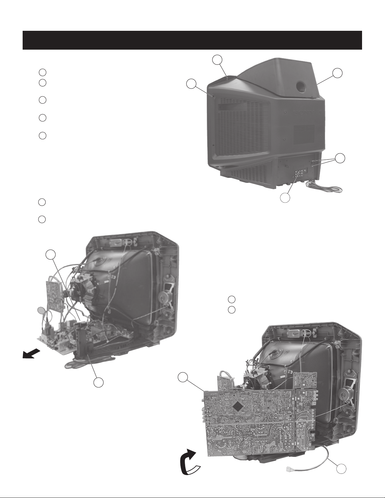
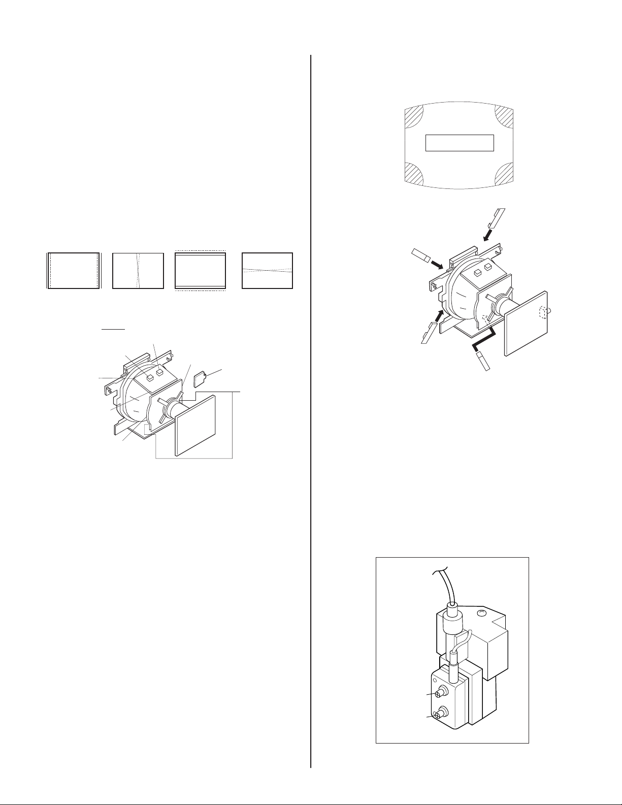
SECTION 1: DISASSEMBLY
KV-21FA350/21FA550
1-1. REAR COVER REMOVAL
1
Lift to remove Subwoofer from top of Rear Cover.
2
Remove screws from top of Rear Cover.
4 Screws +BVTP2 4x16
3
Remove screws from both sides of Rear Cover.
6 Screws +BVTP2 4x16
Remove screw from bottom of Rear Cover.
4
1 Screw +BVTP2 4x16
Remove screws from Speaker Switch and Rear Cover.
5
2 Screws +BVTP 3x12 TYPE2 TT(B)
Slide to remove Rear Cover from Beznet.
1-2. CHASSIS ASSEMBLY REMOVAL
1
Remove J4 Board and Bracket.
One Screw +BVTP 3x12 TYPE2 IT-3
2
Push down claw and slide out A, H2 and W Board.
2
1
3
5
4
2
1-3. SERVICE POSITION
1
Release AC Power cord.
2
Rotate A, H2 and W Boards.
2
1
KV-21FA350/21FA550
1
9
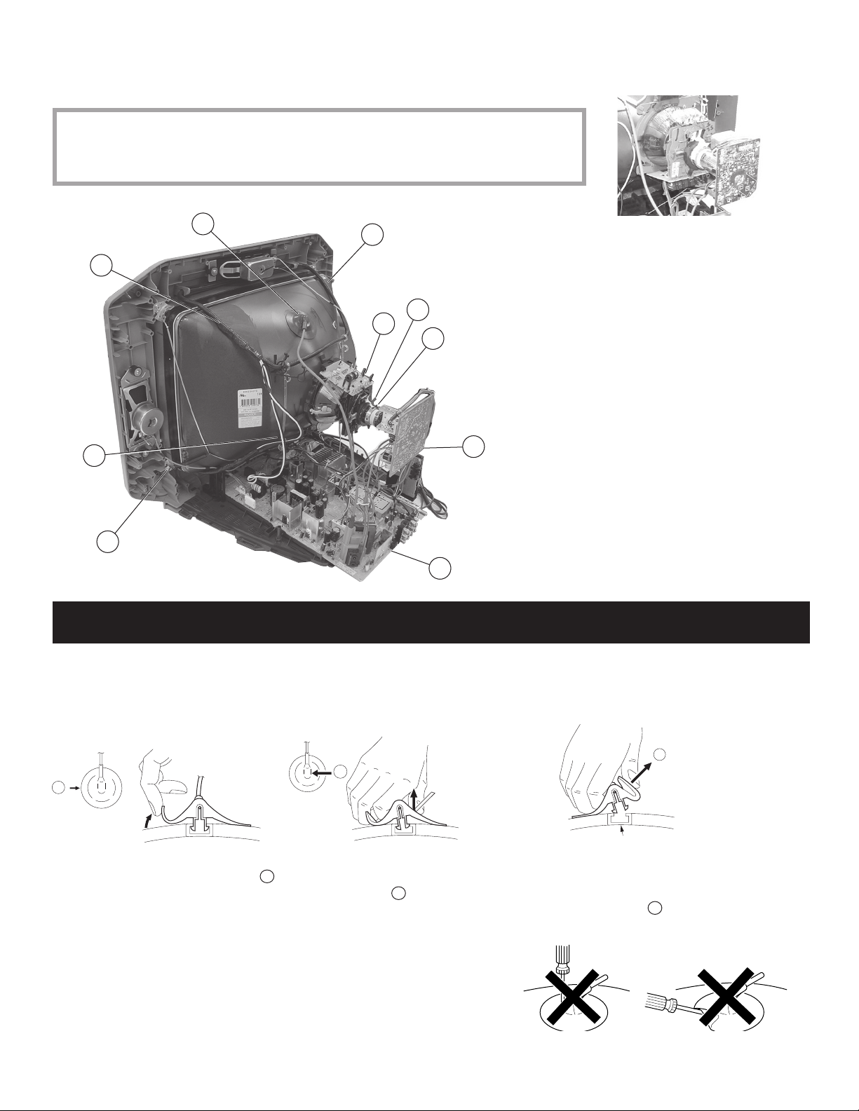
1-4. PICTURE TUBE REMOVAL
WARNING: BEFORE REMOVING THE ANODE CAP
High voltage remains in the CRT even after the power is disconnected. To avoid electric shock,
discharge CRT before attempting to remove the anode cap. Short between anode and CRT
coated earth ground strap.
KV-21FA350/21FA550
1
8
9
10
7
1. Discharge the anode of the CRT and remove
the anode cap.
2. Unplug all interconnecting leads from the
6
2
5
3
4
defl ection yoke, neck assembly, degaussing
coils and CRT grounding strap.
3. Remove the CV Board from the CRT.
4. Remove the chassis assembly.
5. Loosen the neck assembly fi xing screw and
remove.
6. Loosen the defl ection yoke fi xing screw and
remove.
7. Place the set with the CRT face down on
a cushion and remove the degaussing coil
holders.
8. Remove the degaussing coils.
9. Remove the CRT grounding strap and spring
tension devices.
10. Unscrew the four CRT fi xing screws [located on
each CRT corner] and remove the CRT [Take
care not to handle the CRT by the neck].
ANODE CAP REMOVAL PROCEDURE
WARNING: High voltage remains in the CRT even after the power is disconnected. To avoid electric shock, discharge CRT before attempting to remove
the anode cap. Short between anode and coated earth ground strap of CRT.
NOTE: After removing the anode cap, short circuit the anode of the picture tube and the anode cap to either the metal chassis, CRT shield, or carbon
painted on the CRT.
REMOVAL PROCEDURES
c
b
a
Anode Button
Turn up one side of the rubber cap in
the direction indicated by arrow a .
HOW TO HANDLE AN ANODE CAP
1. Do not use sharp objects which may cause damage to the surface of the
anode cap.
2. To avoid damaging the anode cap, do not squeeze the rubber covering too
hard. A material fi tting called a shatter-hook terminal is built into the rubber.
3. Do not force turn the foot of the rubber cover. This may cause the shatterhook terminal to protrude and damage the rubber.
KV-21FA350/21FA550
Use your thumb to pull the rubber
cap fi rmly in the direction indicated
by arrow b .
When one side of the rubber cap separates from
the anode button, the anode cap can be removed
by turning the rubber cap and pulling it in the
direction of arrow c .
10
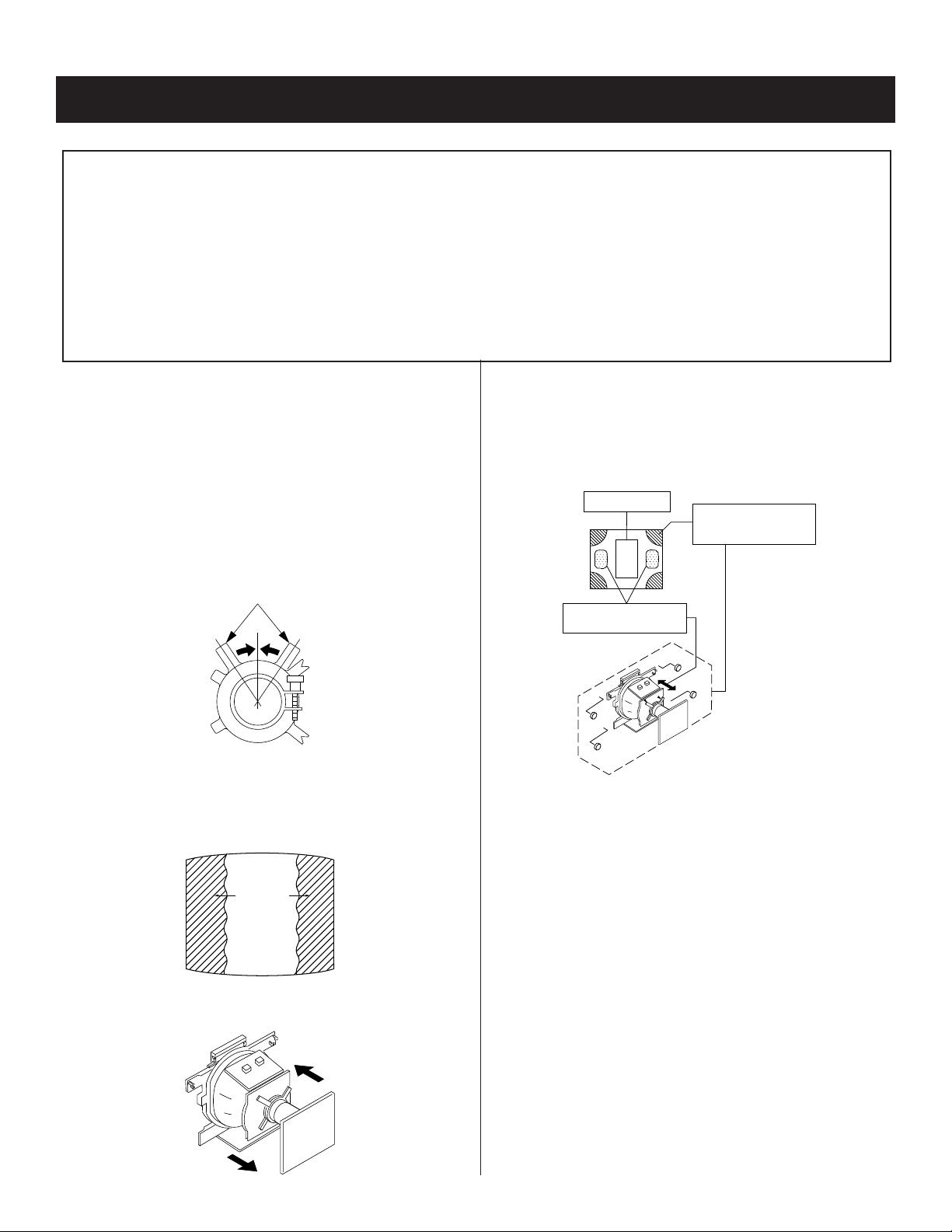
SECTION 2: SET-UP ADJUSTMENTS
KV-21FA350/21FA550
The following adjustments should be made when a complete realignment
is required or a new picture tube is installed.
These adjustments should be performed with rated power supply voltage
unless otherwise noted.
Set the controls as follows unless otherwise noted:
Picture control NORMAL
Brightness control NORMAL
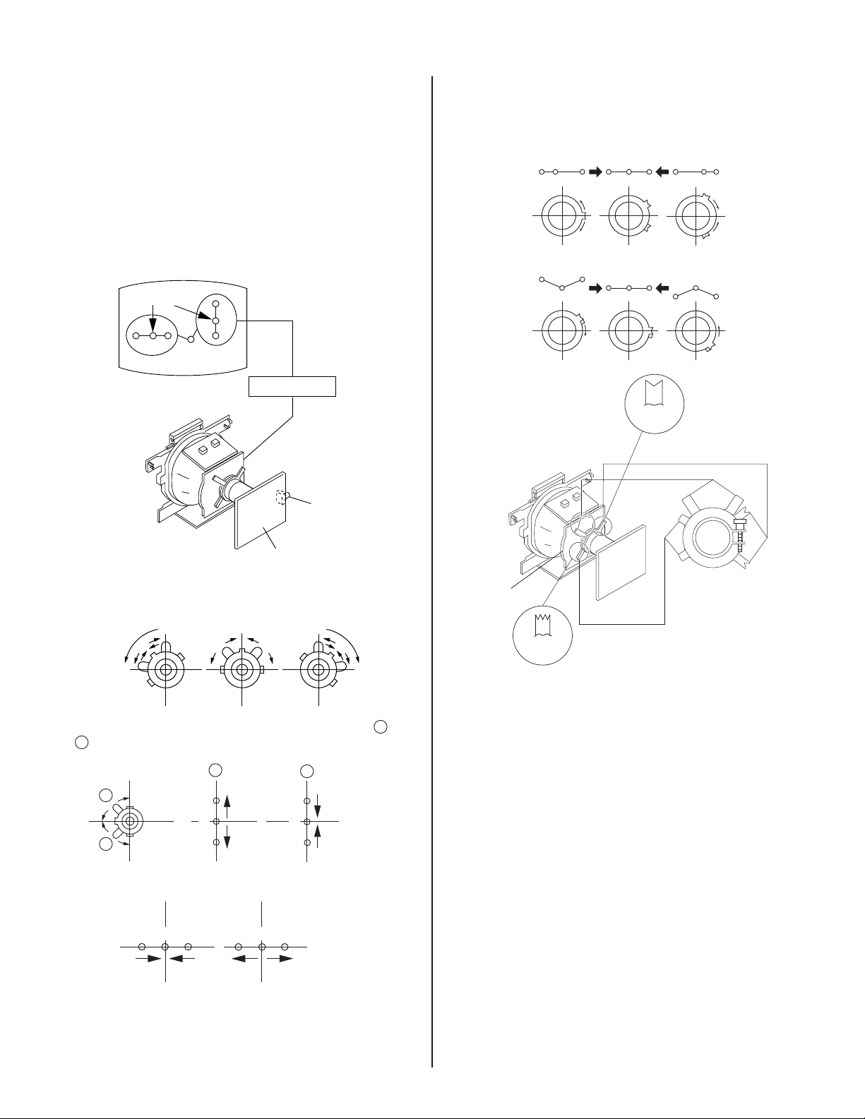
2-1. BEAM LANDING
Before beginning adjustment procedure:
1. Feed in the white pattern signal.
2. In order to reduce the geomagnetism on the set’s picture tube, face
it east or west.
Adjustment Procedure
1. Input a raster signal with the pattern generator.
2. Loosen the defl ection yoke mounting screw, and set the purity
control to the center as shown below:
Purity control
Perform the adjustments in order as follows:
1. Beam Landing
2. Convergence
3. Focus
4. Screen (G2)
5. White Balance
Note Test Equipment Required:
1. Color Bar Pattern Generator
2. Degausser
3. DC Power Supply
5. Oscilloscope
6. Landing Checker
7. XCV Adjuster
4. Digital Multimeter
6. Switch over the raster signal to red and blue and confi rm the
condition.
7. When the position of the defl ection yoke is determined, tighten it
with the defl ection yoke mounting screw.
8. If landing at the corner is not right, adjust by using the disk
magnets.
Purity control
corrects this area.
a
b
d
c
Deflection yoke positioning
corrects these areas.
Disc magnets or rotatable
disc magnets correct these
areas (a-d).
3. Turn the raster signal of the pattern generator to green.
4. Move the defl ection yoke backward, and adjust with the purity
control so that green is in the center and red and blue are even on
both sides.
Blue
Red
Green
5. Move the defl ection yoke forward, and adjust so that the entire
screen becomes green.
b
c
a
d
KV-21FA350/21FA550
11
KV-21FA350/21FA550
2-2. CONVERGENCE
Before starting convergence adjustments:
1 Perform FOCUS, VLIN and VSIZE adjustments.
2. Set BRIGHTNESS control to minimum.
3. Set Picture mode to STANDARD.
4. Feed in dot pattern.
Vertical Static Convergence
1. Adjust the 4 pole magnet to converge red, green and blue dots in
the center of the screen.
Center dot
R G B
R
G
B
4 pole magnet
Horizontal Static Convergence
If the blue dot does not converge with the red and green dots, use the 6
pole magnet to adjust as shown:
RG B R G B R GB
RB
G
RG
RB
6 Pole
Magnet
6 Pole Magnet
Purity
GB
RV750
H. STAT
C/CV Board
2. Tilt the 4 pole magnet and adjust static convergence to open or
close the 4 pole magnet.
When the 4 pole magnet is moved in the direction of arrow A and
B
, the red, green, and blue dots move as shown below:
A
B
A
B
G
R
B
B
G
R
Moved RV750 (H.STAT)
DY pocket
4 Pole
Magnet
4 Pole Magnet
RGGRB
KV-21FA350/21FA550
B
12
KV-21FA350/21FA550
Convergence Rough Adjustment
Before performing this adjustment, perform Horizontal and Vertical Static
Convergence Adjustment.
Input cross hatch pattern.
a) TLH
Adjust the horizontal convergence of red and blue dots by inserting
TLH Correction Plate to the DY pocket (left or right).
b) YCH
Adjust YCH to balance Y axis.
c) TLV
Adjust YCh to balance Y axis.
d) XCV
Adjust XCV to balance X-axis.
YCH
DY pocket
RB
YCH
TLV
B
R
TLV
DY pocket
R
B
TLH Plate
XCV
XCV
B
R
TLH
ON DY:
TLV
XCV
Screen Corner Convergence
Affi x a Piece A (90), Convergence Correct/Permaloy Assy Correction to
the misconverged areas.
ba
a-d : screen-corner
misconvergence
cd
b1
a1
d1
a1~d1:Piece A (90), Convergence Correct
Permaloy Assy Correction
or
c1
2-3. FOCUS
FOCUS adjustment should be completed before White Balance
adjustment. (See 4-4. White Balance Adjustment)
1. Receive digital monoscope pattern.
2. Set Picture Mode to “DYNAMIC”.
3. Adjust focus VR to obtain a just focus at the center of the screen.
4. Change the receiving signal to white pattern and blue back.
5. Confi rm magenta ring is not noticeable. In case magenta ring is
obvious, then adjust FOCUS VR to balance magenta ring and
FOCUS.
KV-21FA350/21FA550
FOCUS
SCREEN
13
2-4. SCREEN (G2)
1. Before beginning adustment procedure:
-Set Picture and Brightness to “STANDARD”.
-Set TV to Video mode.
-Set WHBL 016 “RGBB” to 01
2. Connect R, G, B of the C Board cathode to oscilloscope.
3. Adjust Brightness to obtain the cathode value to the value shown
below:
165 ± 2VDC
4. Adjust SCREEN VR on the FBT until the scanning line disappears.
5. Set WHBL 16 “RGBB” back to 00.
KV-21FA350/21FA550
KV-21FA350/21FA550
14
SECTION 3: CIRCUIT ADJUSTMENTS
Electrical Adjustments by Remote Commander
Use the Remote Commander (RM-YA005) to perform the circuit adjustments in this section.
Test Equipment Required: 1. Pattern generator 2. Frequency counter 3. Digital multimeter 4. Audio oscillator
3-1. REMOTE ADJUSTMENT BUTTONS AND INDICATORS
DISPLAY
(Service Mode)
KV-21FA350/21FA550
MUTING
(Enter into
memory)
1
Display next
Item
2
Display next
Category
4
Display previous
Item
8
(Initialize)
VOLUME (+)
(Service Mode)
POWER
(Service Mode)
3
Increase
Data value
6
Decrease
Data value
5
Display previous
Category
ENTER
(Enter into
memory)
0
(Remove
from memory)
KV-21FA350/21FA550
RM-YA005
15
3-2. ACCESSING THE SERVICE MENU MODE
Use the remote commander to access the service meu mode and perform the following adjusments.
1. Standby mode (Power off).
2. Press the following buttons on the remote commander within a second of each other:
DISPLAY
Channel
5
Sound Volume +
The screen displays the fi rst service data category item.
POWER
KV-21FA350/21FA550
category in decimal item name in decimal NG service command frequency video input name
GEOM 000 HPOZ 055 x SERVICE 60 VIDEO 1
release ID version in binary for factory color system (decimal)
STR31 7.11U 0011 1111 FF FF - - - - - 00084
000 00 00 0000 3E 40 000 004000 0000FF
item no. service data NVM field channel no./
software service data reserved power on time
Status Byte Status Byte
Flash DCXO #1 SSD #2 SSD
1. On the Remote Commander press 2 to select the next category, or 5 to select the previous category.
2. Press 1 to select the next item, or 4 to select the previous item.
3. Press 3 to increase the data value, or 6 to decrease the data value.
4. Press
MUTING
then 0 to write into memory.
GREEN
GEOM 000 HPOS 039 SERVICE 50 VIDEO 1
write with [MUTING].
GREEN
GEOM 000 HPOS 039 WRITE 50 VIDEO 1
Write executed with -.
RED
GEOM 000 HPOS 039 WRITE 50 VIDEO 1
Resetting the User Menus
Use the following procedure to reset the User Menus to the factory default settings.
1. Access Service Adjustment Mode.
2. Press 8 then 0 on the Remote Commander.
“WRITE” displays when
saving changes
“WRITE” becomes red
when saving, then changes
to “SERVICE”
KV-21FA350/21FA550
16
KV-21FA350/21FA550
3-3. CONFIRMING SERVICE ADJUSTMENT
CHANGES
1. After completing adjustments, pull out the plug from the AC outlet,
then replace the plug in the AC outlet again.
2. Access Service Adjustment Mode.
3. Using the buttons on the Remote Commander, locate the adjusted
items again to confi rm they were adjusted.
3-4. WHITE BALANCE ADJUSTMENTS
NOTE: FOCUS adjustment should be completed before White Balance
adjustment. (See 2-3. FOCUS)
1. Access Service Mode.
2. Input white raster signal using signal generator.
3. Set the following condition:
Picture “DYNAMIC”, PICT 006, note value of “WTS”
then change to 00.
4. Press 2 or 5 to select the WHBL category.
5. Press 1 or 4 to display the 03 “GDRV” and 04 “BDRV” items.
6. Press 3 or 6 to adjust for the best white balance.
7. At Cutoff, select WHBL 000 “BKOR” and 001 “BKOG” and adjust
the data.
8. Perform adjustment at Highlight and Cutoff condition until it reaches
its target.
9. Press
10. Set PICT 006 “WTS” back to its original data.
MUTING
then
ENTER
to save into the memory.
10. Set “PWL” and “BLBG” back to initial data.
(“PWL”: 01h and “BLBG”: 00h)
11. Press
Sub Color Adjustment
1. Set TV to Video mode.
2. Set Picture mode to “CUSTOM”.
3. Input PAL 100% Color Bar (CB) to TV set (OTHER MODEL).
4. INPUT NTSC 75% CB to TV set (NTSC MODEL).
5. Set PICT 006 “WTS” to 00h and Intelligent Picture to “OFF”.
6. Set the following condition:
PICTURE 50%, COLOR 50%, BRIGHTNESS 50%, HUE 50%,
7. Connect an oscilloscope to pin
8. Press
MUTING
SHARPNESS 50%
1
or 4 to select SADJ 004 “SCOL”, then adjust
B2=VB3=VB4
V
6
, then write in the data +5 step offset.
VB1
VB2 VB3 VB4 VB1 VB2 VB3 VB4
VB2 = VB3 = VB4 (for PAL) VB1 = VB4 (for NTSC)
then 0 to write into memory.
2
(B Output) of CN004.
(for PAL),
VB1 = VB4 (for NTSC)
(Difference is within 70mV)
by pressing
3
or
3-5. PICTURE QUALITY ADJUSTMENTS
P Max/Contrast Adjustment
1. Set TV to Video mode.
2. Set Picture mode to “CUSTOM”.
3. Input PAL 100% CB to TV set (OTHERS), NTSC 75% CB (NTSC
model).
4. Set PICT 003 “PWL” to 00h WHBL 017 “BLBG” to 01h.
5. Set the following condition:
PICTURE 100%, COLOR 0%, BRIGHTNESS 50%
6. Connect an oscilloscope to pin
1
7. Press
pressing 3 or 6 until the spec below:
or 4 to display SADJ 000 “PMAX”, then adjust VR by
1.46 ± 0.03 Vp-p = For 21" without VM models
1.65 ± 0.03 Vp-p = With VM models except NTSC models
1.23 ± 0.03 Vp-p = NTSC models VM models
1.10 ± 0.03 Vp-p = For 21" NTSC non VM models
4
(R Output) of CN004.
VR
Black
9. Press
10. Set “WTS” back to original data and Intelligent Picture to “ON”.
11. Copy no.9 data to PAL TV & DVD mode.
MUTING
then 0 to write into memory.
Sub Hue Adjustment
1. Set TV to Video mode.
2. Set Picture mode to “CUSTOM”.
3. Input NTSC 3.58 CB to TV set.
4. Set the following condition:
PICTURE 50%, COLOR 50%, BRIGHTNESS 50%, HUE 50%,
SHARPNESS 50%
5. Press 1 or 4 to select service mode and - 5 step offset from SADJ
004 “SCOL”.
6. Connect oscilloscope to pin
7. Press 1 or 4 to select SADJ 001 “SHUE”, then press 3 or 6 to
adjust the data.
8. Press
9. Press 1 or 4 to select SADJ 004 “SCOL” and +5 step offset, then
10. Select TV channel with 3.58 and repeat item (3) to (7) and +1 step
11. Press
MUTING
press
MUTING
data offset.(NTSC model)
MUTING
then 0 to write into memory.
then 0 to write into memory .
then 0 to write into memory.
2
(B output) of CN004.
8. Select Wide Mode to “ON” in TV and Video mode and write “PMAX”
data - 8 steps (for models with V-Compression features only).
9. Press
MUTING
then 0 to write into memory.
KV-21FA350/21FA550
17
KV-21FA350/21FA550
12. For single system model with NTSC 4.43, select TV channel with
NTSC 4.43 and repeat items (3) to (8)
VB3
VB1
VB2
VB4
80mV
The highest level of VB1, VB2, VB3, VB4
must be aligned at the same time.
The ideal difference between
V
B2 and VB3 is within ± 80mV
13. Once adjustment is completed in Video mode, carry out adjustment
in DVD mode. Set TV to DVD mode. Input NTSC 3.58 CB to DVD
set and perform steps 4 to 9 and 11.
Sub Bright Adjustment
1. Set TV to RF mode.
2. Input PAL monoscope to RF mode.
3. Set Brightness 50% and Picture to “MINIMUM”.
4. Press 1 (or 4) to select WHBL 010 “SBRT”.
5. Press 3 to increase the data value, or 6 to decrease the data value
so that the cut-off level is 10 IRE, slightly glimmer: 20 IRE.
6. Press
MUTING
then 0 to write into memory.
PAL 50Hz Normal Mode
1. Input PAL signal 50Hz in the Service Mode.
2. Set Wide Mode to “OFF”.
3. Perform the below adjustments using the “General Setting”
sequence.
Item No. Function Illustration
GEOM 013 Vertical Shift
(VPOS)
GEOM 011 Vertical Amplitude
(VSIZ)
GEOM 000 Horizontal Shift
(HPOS)
GEOM 009 EW Trapezoid
(EWTZ)
GEOM 005 EW Width (EW)
(HSIZ)
GEOM 002 Horizontal Bow
(HBOW)
Note: Adjust VSIZ to
Note: Adjust HSIZ to
±
(SPCB)
12.4
(PAL Monoscope)
±
11. 3
±
(NTSC Monoscope)
11. 5
±
(SPCB)
16.4
±
(PAL Monoscope)
14.6
±
(NTSC Monoscope)
15.3
Geometry Adjustment
Geometry adjustment must be done for both color systems PAL and
NTSC.
General Setting
1. Input Monoscope or Special Color Bar (SPCB) signal using a
pattern generator.
2. Access Service Mode.
3. Select the category item that needs adjusting by pressing 1 or
4. Press 3 to increase the data value, or 6 to decrease the data
value.
5. Press
MUTING
then 0 to write into memory.
NOTE: Geometry Adjustment must be performed for 4 different modes:
PAL 50Hz NORMAL MODE,
PAL 50Hz WIDE MODE,
NTSC 60Hz NORMAL MODE,
NTSC 60Hz WIDE MODE.
4
GEOM 006 EW Parabola/Width
(EWPW) (PW)
GEOM 007 EW Upper Corner
(UCOP) Parabola
GEOM 008 EW Lower Corner
(LCOP) Parabola
GEOM 001 Horizontal
(HPAR) Parallelogram
GEOM 012 S-Correction(SC)
(SCOR)
GEOM 003 Vertical Linearity
(VLIN)
GEOM 004 Vertical Scroll
(VSCR)
4. After completing the adjustments for PAL 50Hz NORMAL MODE,
set Wide mode to “ON”, and copy all PAL 50Hz NORMAL MODE
adjusted data to PAL 50Hz WIDE MODE except VSCR.
5. Complete the adjustment for NTSC 60Hz NORMAL MODE.
6. Set Wide mode to “OFF”.
7. Complete the adjustment items listed in the above table using the
“General Setting” sequence.
8. After completing the adjustments set Wide mode to “ON” and copy
all NTSC 60Hz NORMAL MODE adjusted data to NTSC 60Hz
WIDE MODE except VSCR.
9. After completing all the adjustments, reconfi rm VSIZ and VPOS.
KV-21FA350/21FA550
18
3-6. SERVICE DATA
Initial Value
Initial Value
KV-21FA350/21FA550
TVJ Function
Category No. Name
GEOM 000 HPOS
Functionality
001 HPAR
002 HBOW
003 VLIN
004 VSCR
005 HSIZ
006 EWPW
007 UCOP
008 LCOP
009 EWTZ
010 VSLP
011 VSIZ
012 SCOR
013 VPOS
014 HBL
015 W BF
016 WBR
017 SBL
018 COPY
Horizontal Shift (HS) 31 31 31 31
Horizontal Parallelogram 31 31 31 31
Horizontal Bow 31 31 31 31
Vertical Linearity 31 31 31 31
Vertical Scroll 31 31 31 31
EW Width (EW) 31 31 31 31
EW Parabola/Width (PW) 31 31 31 31
EW Upper Corner Parabola 17 17 17 17
EW Lower Corner Parabola 17 17 17 17
EW Trapezium 31 31 31 31
Vertical Slope (VS) 31 31 31 31
Vertical Amplitude 15 15 15 15
S-Correction (SC) 14 14 14 14
Vertical Shift (VSH) 31 31 31 31
RGB Blanking Mode 01 01 01 01
Timing of Wide Blanking (WBF) 07 07 07 07
Timing of Wide Blanking (WBR) 10 14 10 14
Service Blanking 00
Copy the GEO data to all 50/60Hz NVM area 00
Common
(4:3) 50 (4:3) 60 (4:3) w50 (4:3) w60
TVJ Function
Category No. Name
WHBL 000 BKOR
Functionality
001 BKOG
002 RDRV
003 GDRV
004 BDRV
005 LPG
006 PGR
007 PGG
008 PGB
009 GNOF
010 SBRT
011 SBRO
012 CBS
013 RGBB
014 BLBG
015 OFB
016 WBP
Black Level Offset R (OFB = 00), Offset B (OFB = 01) 31 31 31 31 31
Black Level Offset G 31 31 31 31 31
White Point R 37 37 37 37 37
White Point G 37 37 37 37 37
White Point B 37 37 37 37 37
RGB Gain Preset 01
Preset Gain R (PGR) 50
Preset Gain G (PGG) 50
Preset Gain B (PGB) 50
Preset Gain Offset 15
Sub-Brightness
Sub-Brightness Offset (Intelligent Pic) 02
Control Sequence of Beam Current Limiting 00
RGB Blanking 00
Blanking of Blue & Green Output 00
Black Level Offset Blue 01
Color Temp setting (0:High , 1:Normal , 2,3: Low)
Common
Col Temp
(Cool other)
Col Temp
(Warm other)
Col Temp
(Neutral other)
Col Temp
(Cool YUV)
Col Temp
(Warm YUV)
KV-21FA350/21FA550
19
KV-21FA350/21FA550
012
CBS
016
WBP
Initial Value
TVJ Function
Category No. Name
WHBL 000 BKOR
TVJ Function
Category No. Name
WHBL 000 BKOR
Functionality
001 BKOG
002 RDRV
003 GDRV
004 BDRV
005 LPG
006 PGR
007 PGG
008 PGB
009 GNOF
010 SBRT
011 SBRO
013 RGBB
014 BLBG
015 OFB
Functionality
001 BKOG
002 RDRV
003 GDRV
004 BDRV
005 LPG
006 PGR
007 PGG
008 PGB
009 GNOF
010 SBRT
011 SBRO
012 CBS
013 RGBB
014 BLBG
015 OFB
016 WBP
Black Level Offset R (OFB = 00), Offset B (OFB = 01) 31
Black Level Offset G 31
White Point R 37
White Point G 37
White Point B 37
RGB Gain Preset
Preset Gain R (PGR)
Preset Gain G (PGG)
Preset Gain B (PGB)
Preset Gain Offset
Sub-Brightness 31 31 31
Sub-Brightness Offset (Intelligent Pic)
Control Sequence of Beam Current Limiting
RGB Blanking
Blanking of Blue & Green Output
Black Level Offset Blue
Color Temp setting (0:High , 1:Normal , 2,3: Low) 00 01
Black Level Offset R (OFB = 00), Offset B (OFB = 01)
Black Level Offset G
White Point R
White Point G
White Point B
RGB Gain Preset
Preset Gain R (PGR)
Preset Gain G (PGG)
Preset Gain B (PGB)
Preset Gain Offset
Sub-Brightness 31 31
Sub-Brightness Offset (Intelligent Pic)
Control Sequence of Beam Current Limiting
RGB Blanking
Blanking of Blue & Green Output
Black Level Offset Blue
Color Temp setting (0:High , 1:Normal , 2,3: Low) 02
Col Temp
Initial Value
50pal(Video)50pal(TV)YUV
TV VideoPic Mode 2 (CUSTOM)
Pic mode 0
(VIVID)
Pic mode 1
(STANDARD)
KV-21FA350/21FA550
20
TVJ Function
SADJ
000
PMAX
001
SHUE
Sub-Hue
002
SSHP
Sub-Sharpness
003
SSHO
Sub-Sharpness Offset (Intelligent Pic)
004
SCOL
Sub-Color
005
SCOO
Sub-Color Offset (Intelligent Pic)
006
PIC
Picture Control [GA:0~100(valid); >100(invalid), Others:0~63(valid); ignore bit 6(invalid)]
007
COL
Color Control [GA:0~100(valid); >100(invalid), Others:0~63(valid); ignore bit 6(invalid)]
6(invalid)]
send to TINT #1Eh(5-0) with US model)
Functionality
Common
Initial Value
YUV
50secam(TV)
50secam(Video)
TV
Video
50pal(TV)
50pal(Video)
SADJ
000
PMAX
001
SHUE
Sub-Hue
002
SSHP
Sub-Sharpness
003
SSHO
Sub-Sharpness Offset (Intelligent Pic)
004
SCOL
Sub-Color
005
SCOO
Sub-Color Offset (Intelligent Pic)
006
PIC
Picture Control [GA:0~100(valid); >100(invalid), Others:0~63(valid); ignore bit
007
COL
Color Control [GA:0~100(valid); >100(invalid), Others:0~63(valid); ignore bit
6(invalid)]
(* send to TINT #1Eh(5-0) with US model)
60YUV
50RGB
60RGB
50YUV
60ntsc(TV)
60ntsc(Video)
60palm(TV)
60palm(Video)
Functionality
Initial Value
SADJ
000
PMAX
001
SHUE
Sub-Hue
002
SSHP
Sub-Sharpness
003
SSHO
Sub-Sharpness Offset (Intelligent Pic)
004
SCOL
Sub-Color
005
SCOO
Sub-Color Offset (Intelligent Pic)
006
PIC
Picture Control [GA:0~100(valid); >100(invalid), Others:0~63(valid); ignore bit 6(invalid)]
80
007
COL
Color Control [GA:0~100(valid); >100(invalid), Others:0~63(valid); ignore bit 6(invalid)]
6(invalid)]
send to TINT #1Eh(5-0) with US model)
Functionality
Initial Value
Category No. Name
Picture Maximum
Brightness Control [GA:0~100(valid); >100(invalid), Others:0~63(valid); ignore bit
008 BRT
Hue Control [GA:0~100(valid); >100(invalid), Others:0~63(valid); ignore bit 6(invalid)] (*
009 HUE
010 SHP
TVJ Function
Category No. Name
Sharpness Control [GA:0~100(valid); >100(invalid), Others:0~63(valid); ignore bit
6(invalid)]
Picture Maximum
KV-21FA350/21FA550
42
06
31 31 00 31
02
Brightness Control [GA:0~100(valid); >100(invalid), Others:0~63(valid); ignore bit
008 BRT
Hue Control [GA:0~100(valid); >100(invalid), Others:0~63(valid); ignore bit 6(invalid)]
009 HUE
010 SHP
TVJ Function
Category No. Name
008 BRT
009 HUE
010 SHP
Sharpness Control [GA:0~100(valid); >100(invalid), Others:0~63(valid); ignore bit
6(invalid)]
Picture Maximum 37 37 37 37
Brightness Control [GA:0~100(valid); >100(invalid), Others:0~63(valid); ignore bit
Hue Control [GA:0~100(valid); >100(invalid), Others:0~63(valid); ignore bit 6(invalid)] (*
Sharpness Control [GA:0~100(valid); >100(invalid), Others:0~63(valid); ignore bit
6(invalid)]
31 31 31 31 31 31
50RGB 60RGB
Pic mode 0
(VIVID)
100 80
56 50 50
50 50 50
50 50 50
60 50 50
Pic mode 1
(STANDARD)
Pic Mode 2
(CUSTOM)
TV Video
07 07
40 42
TV Wide
(4:3)
Video Wide
(4:3)
KV-21FA350/21FA550
21
KV-21FA350/21FA550
Initial Value
Initial Value
TVJ Function
Category No. Name
YC 000 PFRQ
TVJ Function
Category No. Name
YC 000 PFRQ
Functionality
001 RPA
002 RPO
003 YDLY
004 CMAT
005 ACL
006 CB
007 SBO
008 CHSE
009 CLO
010 CTRP
011 QDT
012 BPS
013 TINT
014 TUV
015 BWYC
016 OSB
017 BKC
Functionality
001 RPA
002 RPO
003 YDLY
004 CMAT
005 ACL
006 CB
007 SBO
008 CHSE
009 CLO
010 CTRP
011 QDT
012 BPS
013 TINT
014 TUV
015 BWYC
016 OSB
017 BKC
Peaking Center Frequency and Delay 01
Ratio Pre & Over Shoot 02
Ratio of Positive & Negative Peaks 03
Y-Delay 09 8 09 NIL 09
PAL-SECAM or NTSC (Japan/USA) Matrix 01
Automatic Color Limiting 01
Chroma Bandpass Center Frequency 00
SECAM Black Offset 00
PAL/NTSC Ident Sensitivity 02
Center Frequency of Cloche(Bell) Filter 00
Chroma Trap Mode 00
Second Chroma Trap 00
Bypass of Chroma Base-band Delay Line 00
Base-Band Tint Control 31 31
Tint Control on UV Signals 00
Bandwidth at YC mode for 3.58 MHz color system (BWYC) 00
Width of internal burstkey pulse of chroma demodulator (OSB) 00
Burst Key Position 00 00 00
Peaking Center Frequency and Delay 00
Ratio Pre & Over Shoot 03
Ratio of Positive & Negative Peaks 03
Y-Delay 09 02 09
PAL-SECAM or NTSC (Japan/USA) Matrix
Automatic Color Limiting
Chroma Bandpass Center Frequency
SECAM Black Offset
PAL/NTSC Ident Sensitivity
Center Frequency of Cloche(Bell) Filter
Chroma Trap Mode 01
Second Chroma Trap 00
Bypass of Chroma Base-band Delay Line 01
Base-Band Tint Control 31
Tint Control on UV Signals
Bandwidth at YC mode for 3.58 MHz color system (BWYC)
Width of internal burstkey pulse of chroma demodulator (OSB)
Burst Key Position
Common
NTSC(Video) SECAM(Video)
Others PAL(Video)
PAL(TV) NTSC(TV) SECAM(TV)YUV
SECAM NTSC TVS-INPUT
KV-21FA350/21FA550
22
KV-21FA350/21FA550
007
MVK
Initial Value
007
MVK
Initial Value
011
AAS
Initial Value
011
AAS
Initial Value
TVJ Function
Category No. Name
SYNC 000 SYS
TVJ Function
Category No. Name
SYNC 000 SYS
Functionality
001 FO
002 VID
003 FSL
004 SSL
005 SVID
006 FORF
Functionality
001 FO
002 VID
003 FSL
004 SSL
005 SVID
006 FORF
Synchronization on YSYNC Input 00
Phase 1 Time Constant 03 03
Video Ident Mode 00 00
Forced Slicing Level for Vertical Sync 00
Slicing Level Sync Separator 00 00
Source Selection for Video Identification 00 00
Forced Field Frequency 01
Macro Vision Keying 01
Synchronization on YSYNC Input
Phase 1 Time Constant 00
Video Ident Mode
Forced Slicing Level for Vertical Sync
Slicing Level Sync Separator
Source Selection for Video Identification
Forced Field Frequency
Macro Vision Keying
Common
No Signal
(4:3) 50 (4:3) 60 Others TV VideoYUV
TVJ Function
Category No. Name
PICT 000 CADL
TVJ Function
Category No. Name
PICT 000 CADL
Functionality
001 CFA
002 SOC
003 PWL
004 WHTL
005 GAM
006 WTS
007 TFR
008 COR
009 CORO
010 BKS
Functionality
001 CFA
002 SOC
003 PWL
004 WHTL
005 GAM
006 WTS
007 TFR
008 COR
009 CORO
010 BKS
Cathode Drive Level 00
Comb Filter Mode 00
Soft Clipping Level 00
Peak White Limiting Switch 01
Peak White Limiting 00
Gamma 00
Gamma Control and White Stretch 01 01
DC Transfer Ratio of Luminance Signal 01 01
Coring 00 00 00
Coring Offset (Intelligent Pic) 02
Black Stretch 02
Black Area to Switch off the Black Stretch 01
Cathode Drive Level
Comb Filter Mode
Soft Clipping Level
Peak White Limiting Switch
Peak White Limiting
Gamma
Gamma Control and White Stretch
DC Transfer Ratio of Luminance Signal
Coring
Coring Offset (Intelligent Pic)
Black Stretch
Black Area to Switch off the Black Stretch
Common
Others RGB Live
TV(Others) Video(Dyn) Video(Others)
Color Temp (LOW) Color Temp (NORMAL)Color Temp (HIGH) Color Temp (Others)
KV-21FA350/21FA550
23
KV-21FA350/21FA550
SW
000
SVO
Initial Value
012
TUSO
Initial Value
005
BPBS
Initial Value
004
Initial Value
TVJ Function
Category No. Name
TVJ Function
Category No. Name
VIF 000 OIFD
TVJ Function
Category No. Name
VM 000 RGBD
Functionality
Functionality
001 AGCT
002 STM
003 GD
004 AGCS
005 FFI
006 LNAI
007 LNAT
008 LNSN
009 LNSD
010 LNEX
011 CHTR
Functionality
001 VMA
002 VMAP
003 VMMO
004 CRAO
Function of IFVO/SVO/CVBSI Pin @ 48 02 01 01
Offset IF Demodulator
AGC Take-over 31
Search Tuning Mode 01
Group Delay on CVBS1 Signal 00
IF AGC Speed
Fast Filter IF PLL 00
RF Amp LNA bit initial value 00
RF Amp Threshold Level
RF Amp SN Level Threshold
RF Amp SN Level Drop Threshold
RF Amp check SN Drop Timing
Channel Threshold after Auto Prg to set RF Amp User Mode 25
Sony Tuner used
Delay of RGB Output to VM Output 04
Amplitude of VM Output 00
VM setting (0:High , 1:Low , 2,3: OFF) 00 01 00
VM Mode 01
Coring on SVM 00
TV VideoYUV
Common
35
00
195
03
01
30
00
Common
Pic mode 0
Initial Value
OTHERS TVPic mode 1 Pic Mode 2
TVJ Function
Category No. Name
SDEM 000 FMWS
TVJ Function
Category No. Name
TXT 000 TXV
Functionality
001 QSS
002 BPB
003 HPVC
004 CMCA
Functionality
001
002
003
THD Teletext H-sync Active Edge Shift 00
TBR Teletext RGB Brightness 00
ACQ Teletext Acquisition (Auto-0, PAL-1) 00
TBRM Teletext Mix Mode Brightness 00
Window Selection for FM Demodulator 02
Quasi Split Sound (QSS) Amplifier Mode(N/A for GA multi M system) 01
Bypass of Sound Bandpass Filter 00
Head Phone Volume Control 00
Activate Mono Channel 00
Bypass of sound bandpass filter at stereo mode (BPBS) 01
Teletext Vertical Position for Philips 00
Common
Common
KV-21FA350/21FA550
24
KV-21FA350/21FA550
028
Initial Value
TVJ Function
Category No. Name
SDSP 000
Functionality
BBL BBE Contour 00
001
002
003
004
005
006
007
008
009
010
011
012
013
014
015
016
017
018
019
020
021
022
023
024
025
026
027
BBH BBE Process 00
BBLW BBE Contour Offset 06
SVOF Surround /Effect Mode Volume Offset 04 11 04
LAD Decoder Level Adjust 05
LAM Mono Level Adjust 05
LAN Nicam Level Adjust 22
LAS SAP Level Adjust 05
LAA ADC Level Adjust 00 00
SEF Incredible Mono/Stereo Effect
BAS Main Bass Offset 19
TRE Main Treble Offset 19
EQ1 Equalizer Main Channel Band (100 Hz) Offset 18
EQ2 Equalizer Main Channel Band (300 Hz) Offset 18
EQ3 Equalizer Main Channel Band (1000 Hz) Offset 17
EQ4 Equalizer Main Channel Band (3000 Hz) Offset 19
EQ5 Equalizer Main Channel Band (8000 Hz) Offset 21
BFCT DBE, DUB and BBE Control 00
SCEN SRS3D Center Control 04
SSPA SRS3D Space Control 01
BBHW BBE process offset in WOW mode 00
STRE Treble Offset for surround mode 01
BBHT BBE Offset in TV mode 00
TTRE Treble Offset in TV Mode 02
VBAS Bass Offset depend on user volume 01
VTRE Treble Offset depend on user volume 01
TBAS Bass Offset for TV 00
BBLO BBL Offset depend on User Volume 3
BBHO BBH Offset Depend on Use Volume 3
Common
TV Video
SRS/WOWOff Trusurround
KV-21FA350/21FA550
25
KV-21FA350/21FA550
*
028
Initial Value
Initial Value
TVJ Function
Category No. Name
SDSP 000
Functionality
BBL BBE Contour
001
002
003
004
005
006
007
008
009
010
011
012
013
014
015
016
017
018
019
020
021
022
023
024
025
026
027
BBH BBE Process
BBLW BBE Contour Offset
SVOF Surround /Effect Mode Volume Offset
LAD Decoder Level Adjust
LAM Mono Level Adjust
LAN Nicam Level Adjust
LAS SAP Level Adjust
LAA ADC Level Adjust
SEF Incredible Mono/Stereo Effect 05 03
BAS Main Bass Offset
TRE Main Treble Offset
EQ1 Equalizer Main Channel Band (100 Hz) Offset
EQ2 Equalizer Main Channel Band (300 Hz) Offset
EQ3 Equalizer Main Channel Band (1000 Hz) Offset
EQ4 Equalizer Main Channel Band (3000 Hz) Offset
EQ5 Equalizer Main Channel Band (8000 Hz) Offset
BFCT DBE, DUB and BBE Control
SCEN SRS3D Center Control
SSPA SRS3D Space Control
BBHW BBE process offset in WOW mode
STRE Treble Offset for surround mode
BBHT BBE Offset in TV mode
TTRE Treble Offset in TV Mode
VBAS Bass Offset depend on user volume
VTRE Treble Offset depend on user volume
TBAS Bass Offset for TV
BBLO BBL Offset depend on User Volume
BBHO BBH Offset Depend on Use Volume
ImonoIstereo
04
TVJ Function
Category No. Name
SDEC 000
KV-21FA350/21FA550
Functionality
SPTU Upper Threshold forSAP carrier detection 05
001
002
003
004
005
006
007
008
009
010
011
012
013
014
015
016
017
SPTL Lower Threshold for SAP carrier detection 15
SPTH Noise Threshold for automute of SAP 09
SPHY Hysteresis size for automute of SAP 03
FMTH Noise Threshold for automute of SC2 in FM A2 standard 00
FMHY Hysteresis size for automute of SC2 in FM A2 standard 04
NILE NICAM lower error limit (DDEP) 50
NIUE NICAM upper error limit (DDEP) 200
EPMD DEMDEC Easy Programming (DDEP) 01
STDS Bits multiplexed for ASD and SSS modes 13
OVMA FM overmodulation adaption 00
FLBW FM/AM demodulator filter bandwidth 01
IDMD FM ident speed in SSS mode 01
OVMT Overmodulation level threshold relative to nominal 03
DCXI NICAM DCXO Scaling Control Inverter 00
DCXG NICAM DCXO Scaling Control Gain 00
DCLL NICAM DCXO Scaling Control Limit (L) 00
DCLH NICAM DCXO Scaling Control Limit (H) 00
Common
26
KV-21FA350/21FA550
013
TSYS
019
Initial Value
007
HSYC
009
011
Selectable IF 0:STDSEL(17) 50us deemphasis 1: STDSEL(18) 75us deemph
Initial Value
005
006
005
006
Initial Value
Initial Value
TVJ Function
Category No. Name
OPTM 000
Functionality
ASHT auto shut off timer (data * 5 min) 06
001
002
003
004 MUTE
005
006
007
008 HTXT
009 CMSS
010
011
012 EXBL
014 LNSW
015
016
017
018
OSDB OSD brightness 12
OSDH OSD Horizontal Position 08
OSDV OSD Vertical Position 63 39
RFUL RF Signal Change Counter after Unlocked (Disable when 0fh) 01
RFLK RF Signal Change Counter after Locked (Disable when 0fh) 04
LANG OSD language shipping condition 01
DCXO DCXO Value
DISC target DISCO data for DCXO adjust by color dec
AVUL AV Signal Change Counter after Unlocked (Disable when 0Fh) 04
AVLK AV Signal Change Counter after Locked (Disable when 0Fh) 00
SENH Sound Enhancer Crackling sound c/m (0:Off, 1:On) 01
SPSC SPEED search (0: disable, 1:4times, 2:6times, 3:8times) 01
MULO Audio Mute Port Logic Selection (0:Active High, 1:Active Low) 01
No Signal Mute Switch (1 = enabled) 01
sync separator sw
Sync sw
Extended Blanking Timer to Eliminate White Noise. 06
Memorize TV Sys in NVM at Test Reset [0:B/G, 1:I, 2:D/K, 3:M] (GA Model) 03
Signal Booster Shipping/Test Reset condition (1: Auto, 0:Off) 00
Common
01
47
128
(4:3) 50 (4:3) 60 YUV
Others
00 00
KV-21FA350 ONLY
TVJ Function
Category No. Name
OPTB 001
KV-21FA550 ONLY
TVJ Function
Category No. Name
OPTB 001
Functionality
OPB1 Option 1 (System related) 40
002
003
004
002
003
004
OPB2 Option 2 (Video Signal related) 105
OPB3 Option 3 (Stereo Decoding related) 4
OPB4 Option 4 (Miscellaneous) 24
OPB5 Option 5 (Miscellaneous) 3
OPB6 Option 6 (OSD Language related) 1
Functionality
OPB1 Option 1 (System related) 10
OPB2 Option 2 (Video Signal related) 105
OPB3 Option 3 (Stereo Decoding related) 4
OPB4 Option 4 (Miscellaneous) 28
OPB5 Option 5 (Miscellaneous) 3
OPB6 Option 6 (OSD Language related) 1
Common
Common
TVJ Function
Category No. Name
OPUS 000
TVJ Function
Category No. Name
OPFM 000
Functionality
SOFF stay off (0: follow last memory with AC on, 1: standby with AC on) 01
001
002
003
004
005 OUV
006 CFA2
001
002
003
004
005
006
007
008
010
SPCH Channel Number after Shipping Condition 6
SPCA Cable Selection after Shipping Condition (1 = Cable On) 01
CCBR CC Brightness (only for US) 20
CCHP CC H position (only for US) 13
Functionality
FMCT FM Radio Auto Scan Carrier Threshold 20
RPST Waiting time for each frequency step during radio preset 10
MPTU Upper Threshold for MPX pilot detection (FM_RADIO) 12
DCOU Upper threshold for DC offset from FM demodulator 140
DCOL Lower threshold for DC offset from FM demodulator 114
OVMA FM overmodulation adaption (FM_RADIO) 00
FMBR OSD Brightness during FM Mode 12
RTRE Treble Offset in FM Radio Mode 03
RBAS Bass Offset in FM Radio Mode 02
AGCT ACG takeover in FM Radio Mode 32
FLBW FM/AM demodulator filter bandwidth 01
STDS
Offset Control on UV Input Signals (only for NTSC model)
Forced Comb Filter On (only for NTSC model) 00
H Sync Selection for Tuning (SL, LOCK or SID) only for US 01
Initial Value
Common
Common
01
KV-21FA350/21FA550
27
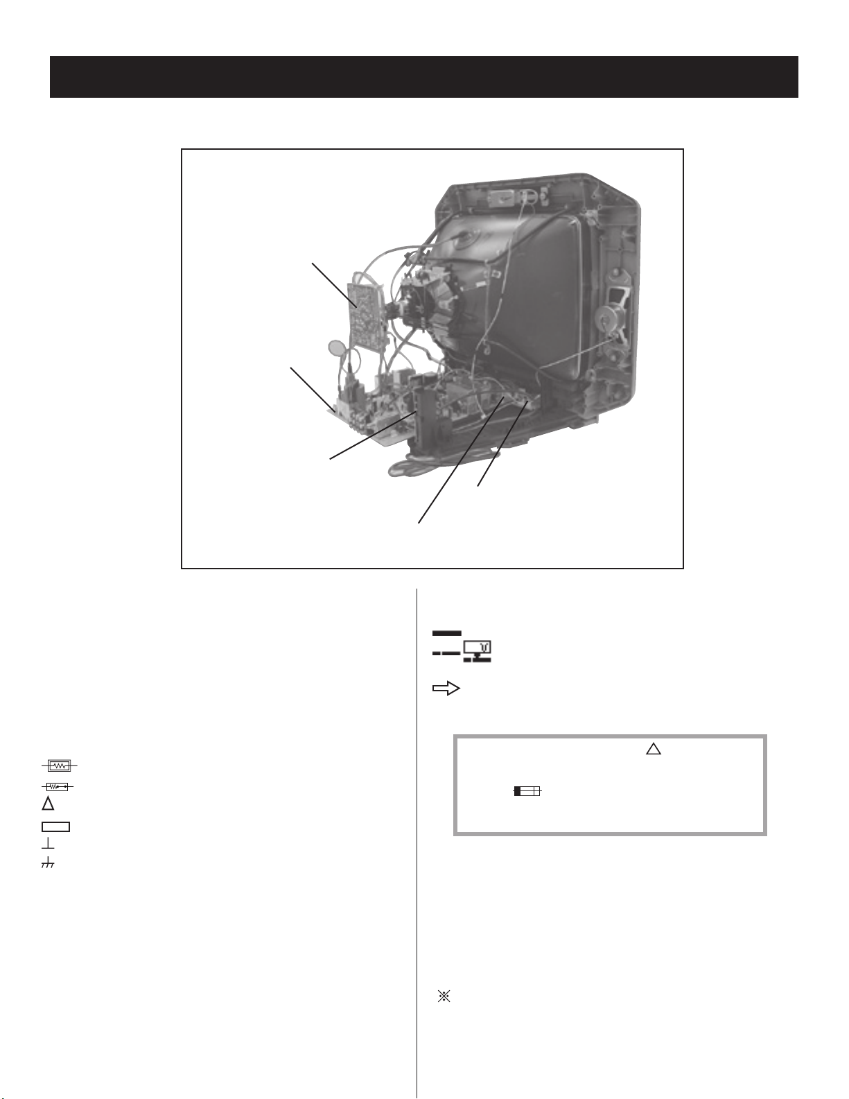
4-1. CIRCUIT BOARDS LOCATION
CV Board
A Board
KV-21FA350/21FA550
SECTION 4: DIAGRAMS
H2 Board
4-2. PRINTED WIRING BOARD AND
J4 Board
SCHEMA
All capacitors are in μF unless otherwise noted. pF : μμF 50WV or less
are not indicated except for electrolytics and tantalums.
All electrolytics are in 50V unless otherwise specifi ed.
All resistors are in ohms. k=1000, M=1000k
Indication of resistance, which does not have one for rating electrical
power, is as follows: Pitch : 5mm Rating electrical power :
1
/
W in resistance, 1/
4
: nonfl ammable resistor.
: fusible resistor.
: internal component.
: panel designation and adjustment for repair.
: earth ground
: earth-chassis
All variable and adjustable resistors have characteristic curve B, unless
otherwise noted.
Readings are taken with a color-bar signal input.
Readings are taken with a 10M digital multimeter.
Voltages are DC with respect to ground unless otherwise noted.
Voltage variations may be noted due to normal production tolerances.
TIC DIAGRAM INFORMATION
W and 1/
10
W in chip resistance.
8
W Board
All voltages are in V.
S : Measurement impossibillity.
: B+line.
: B-line.
(Actual measured value may be different).
: signal path. (RF)
Circled numbers are waveform references.
The components identifi ed by shading and
safety. Replace only with part number specifi ed.
The symbol indicates a fast operating fuse and is displayed on
the component side of the board. Replace only with fuse of the same
rating as marked.
!
symbol are critical for
REFERENCE INFORMATION
RESISTOR
: RN METAL FILM
: RC SOLID
: FPRD NONFLAMMABLE CARBON
: FUSE NONFLAMMABLE FUSIBLE
: RW NONFLAMMABLE WIREWOUND
: RS NONFLAMMABLE METAL OXIDE
: RB NONFLAMMABLE CEMENT
: ADJUSTMENT RESISTOR
COIL
: LF-8L MICRO INDUCTOR
CAPACITOR
: TA TANTALUM
: PS STYROL
: PP POLYPROPYLENE
: PT MYLAR
: MPS METALIZED POLYESTER
: MPP METALIZED POLYPROPYLENE
: ALB BIPOLAR
: ALT HIGH TEMPERATURE
: ALR HIGH RIPPLE
KV-21FA350/21FA550
28
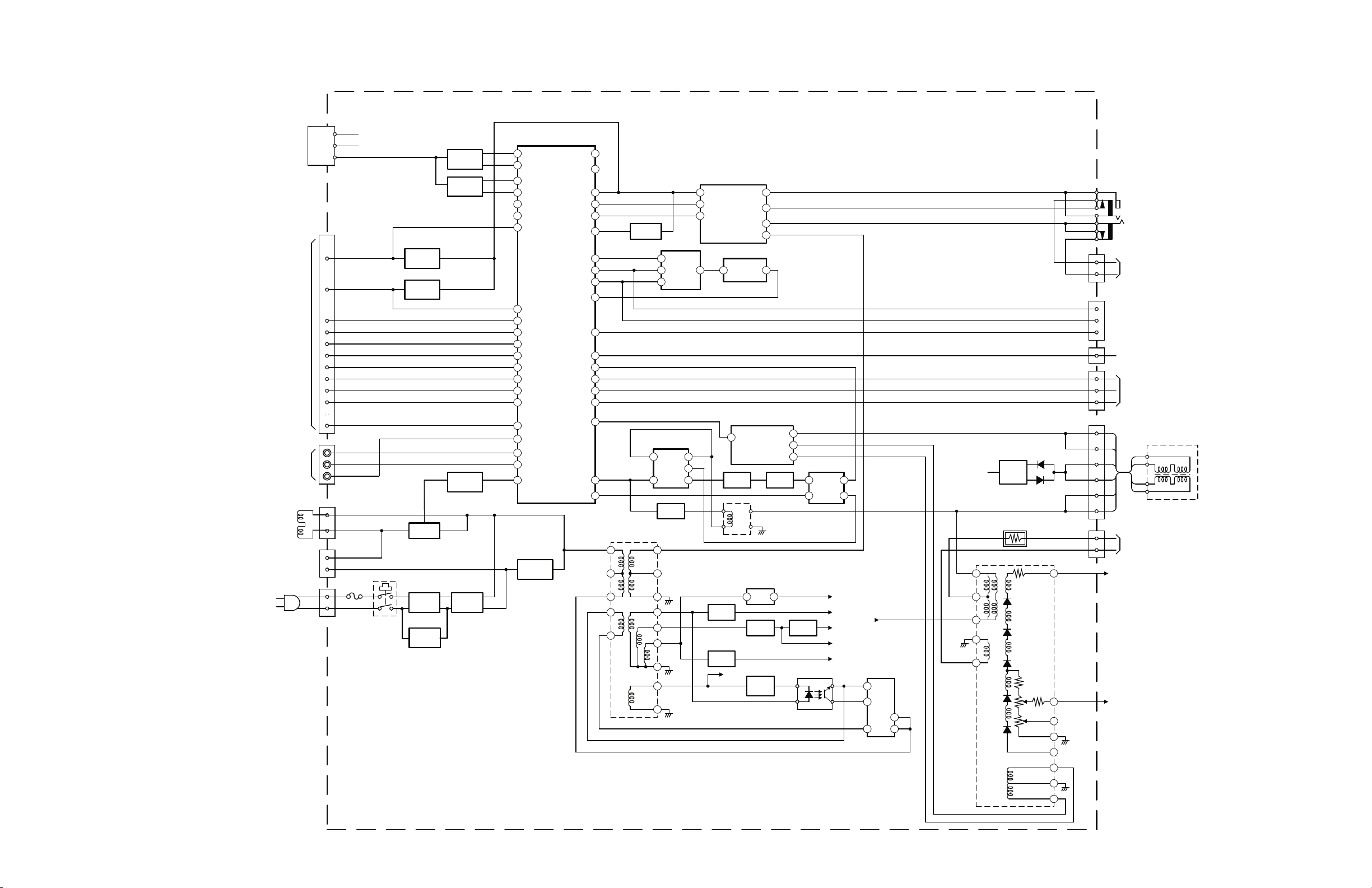
4-3. BLOCK DIAGRAM
SIGNAL FLOW BLOCK DIAGRAM
SCART
FRONT
SOCKETS
AC IN
AC IN
TU101
IF OUT
CN901
J903
CN600
CN601
CN602
SCL
SDA
P16
P15
P7
P9
P3
P5
P11
P10
P12
P14
P1
2
1
2
1
1
2
SCL
SDA
ROUT
LOUT
RIN3
LIN3
RIN1
LIN1
U-OUT
Y-OUT
VOUT
VOUTMON
VIN1
R2
L2
V2
DGC T
DGC T
DGC
DGC
F600
5A
250V
S600
MUTE
SWITCH
Q902
MUTE
SWITCH
Q901
RELAY
RY600
LINE
FILTER
T600
LINE
FILTER
T604
S W F 100
S W F 101
RELAY
SWITCH
Q601
LINE
FILTER
T603
IC001
SY S TE M CONTR OLLE R ,
VIDEO & AUDIO PR OCE SS OR
24
VIF IN 1
25
VIF IN 2
29
SIFIN1
30
SIFIN2
62
SCART HPR
63
SCART HPR
37
OUT R
ROTSW
ROTCTRL
MUTE
LSR
LSL
MO MUTE AUDIO
SDA1
SCR0
SDA0
SIRSC
36
OUT L
54
IN R3
53
57
56
80
79
78
48
58
51
50
49
115
B-Y/BIN
CVBS2/Y2
IN L3
IN R1
IN L1
Y/GIN
R-Y/RIN
MON OU T
CVBS1/-/1
INR 2
INL 2
DGC R E LAY
BINT
KEY
EWD
BOUT
GOUT
ROUT
VD-
HOUT
VD+
MAIN
RECTIFIER
D604
KV-21FA350/21FA550
POWER SUPPLY,
A( )
113
112
IC003
NVM
8
2
5
8
61
5
106
61
60
104
99
108
109
97
102
119
21
87
86
85
22
67
23
SWITCH
Q016
7
6
5
IC801
COMP AR AT O R
3 7
SWITCH
Q803
T602
SRT
1
3
5
7
8
18
17
16
15
14
13
12
11
10
AUDIO 1
AUDIO, DE F LE C TIO N,
IC200
AUDIO AMPLIFIE R
MUTE
PW GND
IN R/NC
IN L
OUT L
OUT R /NC
IC002
IR R E CE IV E R
I O
VERTICAL DEFLECTION
BOOSTER
1
DRV -IN
Q806
Q807
T800
1 4
63
18V R E G ULAT OR
1 2
IC606
3.3V R E G
IC607
2V RE G
+B
TUNER, JACK
9
7
12
10
VCC
OUTVCC
IC804
OUTPUT
VSS
VCC
Q808
IC603
IC602
9V RE G
IC605
ERROR
AMP
5
4
2
IC604
5V RE G
ISO LAT OR
PIN AMP
5
3
PHY600
IC802
1
7
1.8V AUDIO
+3. 3V
+5V
+9V
+1. 8V MA IN
+B
IC601
SWITCHING
REGULATOR
2
5
4 3
J200
HEADP HONE S
CN200
SPL
1
SPR
BINT
BDAT
BCLK
KEY
BOUT
GOUT
ROUT
D821
SWITCH
8V
S800
D819
TO SPE AKERS
4
CN904
2
3
4
CN005
3
TO C ONTROL P ANEL
CN004
2
3
TO C BOARD
4
DY800
6
5
4
3
2
CN701
H.DY
H.DY
V.DY
V.DY
DY
1
CN801
200V
1
4
TO C BOARD
CN703
H1
T801
1
4
2
6
5
1
HV
FV
SV
13
11
9
8
7
TO PICT UR E TUBE
TO C BOARD
FV
J751
KV-21FA350/21FA550
29
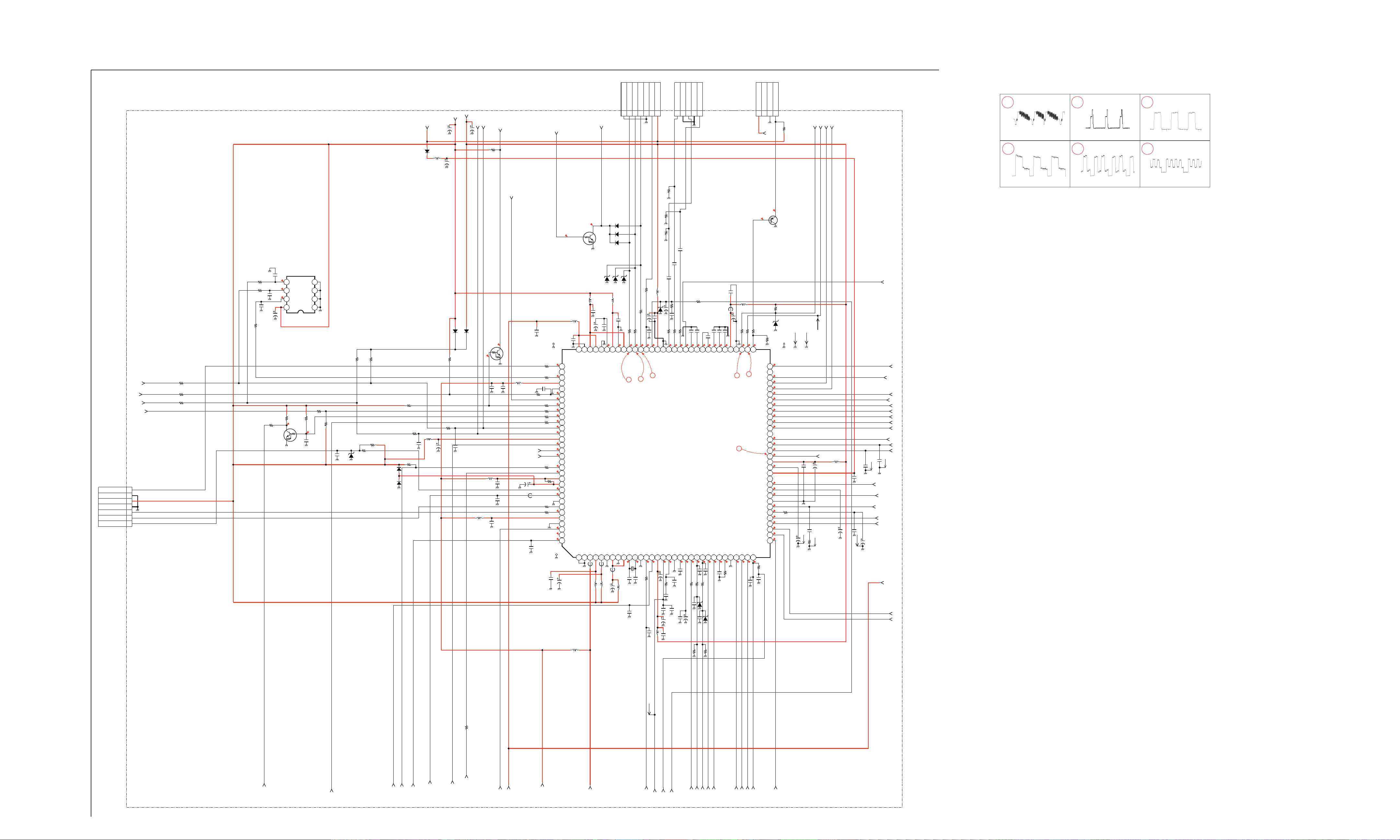
4-4. SCHEMATICS AND SUPPORTING INFORMATION
A BOARD SCHEMATIC DIAGRAM (1 OF 6)
1 | 2 | 3 | 4 | 5 | 6 | 7 | 8 | 9 | 10 | 11 | 12 | 13 | 14 | 15 | 16 | 17 | 18 |
A
—
B
—
D066
PG102R
KV-21FA350/21FA550
TO CV BOARD
CN701
TO A BOARD
CN905
TO CV BOARD
CN711
A BOARD WAVEFORMS
GNDIK9V
CN007
5P
YOUT
GND
U OUT / FB
GND
12345
CN003
4P
VOUT
+BNCGND
123
+B
VM OUT
4
LSL-AUDIO
AFC-DEFL
LSR-AUDIO
R377
1.5k
1/10W
RN-CP
HOUT-DEFL
321
2.5 Vp-p (V) 5.4 Vp-p (H) 3.2 Vp-p (H)
4
5 6
CN004
7P
WHT
GND
BOUT
GOUT
ROUT
5V
3.3V
C005
100
16V
SDA-0
9V
C006
470
10V
L003
C004
10uH
100
16V
SCL-0
R394
4.7k
1/10W
RN-CP
MOMUTE-AUDIO
PWR-OFF-MUTE
RGB
1234567
C
—
D
—
E
—
F
—
G
—
H
—
I
—
J
—
K
—
L
—
M
CN006
7P
WHT
TO H2 BOARD
CN4113
SIRCS
GND
GND
LED G
LED R
VCC
KEY
B_CLK
B_INT
B_DAT
AUDIO-STDBY
7
6
5
4
3
2
1
R099
220
1/10W
RN-CP
R096
220
1/10W
RN-CP
R097
1/10W
RN-CP
R388
75
1/10W
D1_JP/MODE2_EU/MONSW-MONO
D025
C028
0.1
16V
47
1608
25V
GNDA
VDDA(1.8)
VDDA3(3.3V)
VREF_POS_LSL
FB006
0uH
L045
10uH
D057
MA111-TX
MA111-TX
MA111-TX
D024
MA8091-M-TX
MA8091-M-TX
L046
10uH
B
0.1
VREFAD
VREFAD_PO
VREF_NEG_LSL+LSR
VREF_POS_LSR+HPL
FB007
0uH
C029
470
10V
D058
D059
D023
R041
100
1/10W
RN-CP
C030
0.22
16V
R039
B
100
1608
1/10W
R038
RN-CP
100
1/10W
RN-CP
0.1
1.6
BOUT
VDDA(3.3V)
VREFAD_NE
6
vREF_NEG_HPL+HPR
VREF_POS_HPR
XTALIN
2.3
C032
10p
50V
CH
1608
C034
10p
&
50V
L047
10uH
CH
1608
C321
0.01
25V
B
1608
1.6
GOUT
5
XTALOUT
2.3
X001
0MHz
R011
470
1/10W
RN-CP
C036
C301
470p
1608
Q001
KRC102S
0.0
C003
100p
50V
CH
1608
R004
100
1/10W
RN-CP
R002
100
1/10W
RN-CP
R393
1/10W
RN-CP
220
3.6
C001
100p
50V
3.6
CH
1608
C318
0.1
16V
B
1608
100
R014
100
1/10W
RN-CP
3.3
8765
C002
470
16V
R342
3.3k
1/10W
RN-CP
CAT24C16WI-GT3
0.0
Q018
RT1N141C-TP-1
MUTE
IC003
NVM
R340
10k
1/10W
RN-CP
2.4
C020
1608
4321
D002
MA111-TX
D003
Q016
KRC102S
MA111-TX
MUTE
0.0
L042
10uH
2.4
C312
1000p
50V
1608
C313
1000p
50V
B
B
1608
L012
C014
10uH
0.22
16V
B
1608
C082
0.22
16V
B
1608
C018
0.01
25V
B
1608
R003
R001
4.7k
4.7k
1/10W
1/10W
RN-CP
RN-CP
R336
4.7k
1/10W
D071
RN-CP
C091
100p
1608
R320
4.7k
1/10W
RN-CP
D072
MA111-TX
R030
100
1/10W
RN-CP
50V
CH
R324
0
CHIP
R338
2.2k
1/10W
RN-CP
R015
R380
100
1/10W
RN-CP
1.5k
1/10W
RN-CP
0.1
16V
B
D068
MA8056-M-TX
C308
0.01
25V
B
1608
MA111-TX
L009
10uH
C311
R010
10k
1/10W
RN-CP
R029
100
1/10W
RN-CP
C090
100p
50V
2.2
50V
1608
CH
L041
10uH
C328
1608
R339
100
1/10W
RN-CP
ROT_CTRL
ROT_SW
C013
100
16V
&
FB021
0uH
2012
0.01
25V
B
R012
1/10W
RN-CP
2.2k
C023
2.2
TP03 TP04
16V
F
2012
R323
100
1/10W
2.9
RN-CP
R018
100
1/10W
RN-CP
0
1/10W
RN-CP
C022
0.22
16V
1608
R025
B
97
98
3.3
99
C021
100
100p
50V
CH
101
1608
3.3
102
0.7
103
2.4
104
2.7
105
0.0
106
3.3
107
3.2
108
3.3
109
110
4.9
111
0.0
112
0.0
113
114
0.0
115
0.0
116
117
118
1.8
119
3.3
120
121
122
3.5
123
100
124
125
3.3
126
0.0
127
3.3
128
TP02
C024
22
50V
C325
0.022
25V
1608
1/10W
RN-CP
R337
1/10W
RN-CP
R341
100
1/10W
RN-CP
R026
1/10W
RN-CP
B
R020
100
470
R024
100
1/10W
RN-CP
JR1011
100
CHIP
2.2
SW VM
MA8091-M-TX
L006
10uH
C025
0.22
C026
16V
B
1608
L043
10uH
VDDA2
VSSADC
SIRCS
VDDADC(1.8)
SCL1
SDA1
VDDC2
VSSC2
BINT
D1_JP/MODE2_EU/MONSW-MONO
MOMUTE-AUDIO
AUDIO STDBY
AUDIO MUTE
SW
SCL0
SDA0
VDDP(3.3V)
S1/VC(GA)
ROT CTRL
ROT SW
STBY_SW
DGC RELAY
H.Pout
VDDC1(1.8V)
DECV1V8
KEY
S2
VSSC1/P
RED LED
GREEN LED
VDDC3(1.8V)
VSSC3
AGC-MUTE
NVM16K/32K
M-SYS-IF
VSSP2
VSSC4
VDDC4(1.8V)
1234567891011121314151617181920212223242526272829303132
FB005
0uH
L040
10uH
L044
10uH
RN-CP
R389
75
1/10W
RN-CP
R387
75
1/10W
RN-CP
C331
0.1
16V
B
1608
C330
0.1
16V
B
1608
C329
0.1
16V
B
R042
1608
2.2k
1/10W
RN-CP
L007
10uH
R364
C037
D075
1/10W
4.7
RN-CP
50V
MA8091-M-TX
C038
100
0.1
16V
16V
C302
B
2.2
1608
50V
CH
1.6
IK
ROUT
R385
100
1/10W
RN-CP
3.2
2.9
VP3
ABL
GND3
4
IC001
TDA12011H/N1F3F
16V
2012
R384
100
1/10W
RN-CP
B-Y/BIN
MICRO/AV PROCESSOR
VSSA1
VGUARD
DECDIG
VP1
PH2LF
PH1LF
1.9
2.6
0.1
C304
100
16V
R044
12k
1/10W
RN-CP
C044
2.2
16V
2012
C041
2200p
50V
B
1608
C317
220
16V
C042
0.22
16V
C322
1000p
50V
1608
B
1608
L008
B
10uH
0.9
0.3
C054
0.1
16V
UIN
VSC
FB008
0uH
C096
16V
1608
1.3
2.4
B
1608
L005
10uH
C056
100
16V
R058
0.1
100
R056
1/10W
B
100
RN-CP
HOUT
VSSCOMB
1
IFVO/IF_MON_OUT
SIFIN1
SIFIN2
1.9
C323
0.01
50V
CH
2012
1.4
0.5
6566676869707172737475767778798081828384858687888990919293949596
AFC
2
SIFAGC/SCART
MONO_OUTL
AGCOUT
3.5
1.9
R059
1k
1/10W
RN-CP
0.3
VM
CVBS0
SCARTHPR
SCARTHPL
CVBS1/Y1
CVBS3
CVBS2/Y2
MON-OUT
AGC2SIF
VCC8V
INTC0-IF
GND2
DECSDEM
OUTR
OUTL
WRIN
WLIN
AVL/2SIF
EHT0
0.6
C058
1000p
50V
1608
LSR
INR1
INL1
INR3
INL3
INR2
INL2
VP2
PLLIF
1/10W
RN-CP
B
LSL
R060
C1
C2
100
VIN
IREF
R051
39k
1/10W
RN-CP
1.3
2.0
1/10W
RN-CP
VDDCOMB
GNDIF
3
1k
R356
0
CHIP
C092
0.1
R386
16V
1.3
C046
6800p
25V
1608
25V
B
1608
R-Y/RIN
SECPLL
C048
0.22
16
B
1608
B
1.3
2.3
V
R045
C050
R314
6.8k
1/10W
RN-CP
100
1/10W
RN-CP
50V
B
1608
0.1
SCARTFBL
DECBG
2.3
C052
1000p
1608
C081
1000p
1608
10
C093
16V
1608
0.1
VOUT
EWD
4.3
50V
B
R046
1/10W
RN-CP
50V
B
C080
1000p
50V
1608
100
1/10W
RN-CP
F
1.3
Y/GIN
GND1
2.3
F
C083
2700p
50V
B
1608
C049
0.022
0.1
B
UOUT
VD-
100
B
C053
0.022
25V
1608
0.1
YOUT
VD+
1.6
D065
C095
C094
0.1
16V
16V
B
1608
1608
B
1.3
1.8
2.0
YIN
YSYNC
VIFIN1
VIFIN2
1.6
2.0
2.0
C089
1000p
50V
B
1608
R048
C055
100
0.15
1/10W
250V
RN-CP
PP
MA8056-M-TX
D064
MA8056-M-TX
R315
6.8k
1/10W
RN-CP
0.1
B
R317
3.3k
1/10W
RN-CP
R395
100k
1/10W
RN-CP
64
63
62
61
60
59
58
57
56
55
54
53
52
51
50
49
48
47
46
45
44
43
42
41
40
39
38
37
36
35
34
33
Q010
2SA1235TP-1EF
D301
MA8091-M-TX
2.0
3.5
3.5
3.5
1.6
1.4
2.2
2.2
1.8
2.2
2.2
1.8
2.2
2.2
2.0
2.3
2.3
1.9
2.0
2.4
JR1012
2.2
3.5
3.5
3.5
3.5
0.1
CHIP
SCARTFBL/A16
W003
W066
W067
CVBSO
SCARTHPL
C1
CVBS1/Y1
INR1
INL1
CVBS3
INR3
INL3
CVBS2/Y2
INR2
MON-OUT
L004
47uH
C303
C072
100
0.01
16V
25V
B
1608
0
C316
0.47
10V
B
1608
W030
C064
W031
2.2
R379
50V
68k
1/10W
RN-CP
C073
2.2
50V
C063
1608
W033
C319
47p
50V
CH
1608
C069
0.1
16V
B
1608
W010
0.1
16V
B
C065
3.3
50V
W065
C320
47p
50V
CH
1608
IFVO/IF_MON_OUT
PLLIF
MONO_OUTL
OUTR
OUTL
1.8V_AUDIO
INL2
W_R_IN
W_L_IN
1.6 Vp-p (H) 1.8 Vp-p (H) 2.0 Vp-p (H)
KV-21FA350/21FA550
—
N
—
O
—
P
A1/6
AUDIO-VIDEO PROCESSOR
MICRO
AUDIO-MUTE
W011
R027
100
1/10W
RN-CP
S2
SW
STBY_SW
DGC-RELAY
M-SYS-IF
S1/VC
H.P_OUT
AGC-MUTE
1.8V_AUDIO
1.8V_MAIN
VDDC4_CAP
PH2LF
VGUARD-DEFL
VZOOM
ABL
EWD-DEFL
VD--DEFL
VD+-DEFL
VIFIN2-IF
VIFIN1-IF
SIFIN1-IF
SIFIN2-IF
TUAGC-IF
OCP-PROTECT
2SIF
A-1237-118-A A-1237-745-A
A-1231-036-A <BX1S>A-P1A-1231-018-A
30
 Loading...