Sony KLV-40BX300 Schematic

HISTORY INFORMATION FOR THE FOLLOWING MANUAL:
SERVICE MANUAL
MODEL NAME REMOTE COMMANDER DESTINATION
KLV-32BX300
KLV-32BX300
KLV-40BX400
KLV-40BX400
RM-YD035 AR
RM-YD035 LATIN AMERICA
RM-YD035 AR
RM-YD035 LATIN AMERICA
AZ1-A
CHASSIS
LEVEL
CONFIDENTIAL
3
ORIGINAL MANUAL ISSUE DATE: 3/2010
REVISION DATE SUBJECT
3/2010 No revisions or updates are applicable at this time.
LCD DIGITAL COLOR TV
9-883-845-51

KLV-32BX300/40BX400
TABLE OF CONTENTS
SECTION TITLE PAGE
Safety-Related Component Warning ..........................................................................................................................................................................3
Safety Check-Out ....................................................................................................................................................................................................... 5
SECTION 1: DIAGRAMS ................................................................................................................................................................................................... 6
1-1. Circuit Boards Location ...................................................................................................................................................................................... 6
1-2. Printed Wiring Boards and Schematic Diagrams Information ............................................................................................................................ 6
1-3. Block Diagram .................................................................................................................................................................................................... 8
1-4. Schematics and Supporting Information ............................................................................................................................................................9
BAA Board Schematic Diagram (1 of 9) ............................................................................................................................................................. 9
BAA Board Schematic Diagram (2 of 9) ........................................................................................................................................................... 10
BAA Board Schematic Diagram (3 of 9) ........................................................................................................................................................... 11
BAA Board Schematic Diagram (4 of 9) ........................................................................................................................................................... 12
BAA Board Schematic Diagram (5 of 9) ........................................................................................................................................................... 13
BAA Board Schematic Diagram (6 of 9) ........................................................................................................................................................... 14
BAA Board Schematic Diagram (7 of 9) ........................................................................................................................................................... 15
BAA Board Schematic Diagram (8 of 9) ........................................................................................................................................................... 16
BAA Board Schematic Diagram (9 of 9) ........................................................................................................................................................... 17
G2HE Board Schematic Diagram (KLV-40BX400 ONLY) ................................................................................................................................ 20
G2LE Board Schematic Diagram (KLV-32BX300 ONLY) ................................................................................................................................. 22
H2LR Board Schematic Diagram ..................................................................................................................................................................... 24
H2LS Board Schematic Diagram ..................................................................................................................................................................... 26
SECTION 2: ELECTRICAL PARTS LIST ........................................................................................................................................................................ 27
APPENDIX A: ENCRYPTION KEY COMPONENTS ..................................................................................................................................................... A-1
KLV-32BX300/40BX400
2

SAFETY-RELATED COMPONENT WARNING
KLV-32BX300/40BX400
There are critical components used in LCD color TVs that are important for safety. These components are identifi ed with shading and
mark on the schematic diagrams and the electrical parts list. It is essential that these critical parts be replaced only with the part number
specifi ed in the electrical parts list to prevent electric shock, fi re, or other hazard.
NOTE: Do not modify the original design without obtaining written permission from the manufacturer or you will void the original parts and
labor guarantee.
!
USE CAUTION WHEN HANDLING THE LCD PANEL
When repairing the LCD panel, be sure you are grounded by using a wrist band.
When installing the LCD panel on a wall, the LCD panel must be secured using the 4 mounting holes on the rear cover.
To avoid damaging the LCD panel:
do not press on the panel or frame edge to avoid the risk of electric shock.
do not scratch or press on the panel with any sharp objects.
do not leave the module in high temperatures or in areas of high humidity for an extended period of time.
do not expose the LCD panel to direct sunlight.
avoid contact with water. It may cause a short circuit within the module.
disconnect the AC adapter when replacing the backlight (CCFL) or inverter circuit.
(High voltage occurs at the inverter circuit at 650Vrms.)
always clean the LCD panel with a soft cloth material.
use care when handling the wires or connectors of the inverter circuit. Damaging the wires may cause a short.
protect the panel from ESD to avoid damaging the electronic circuit (C-MOS).
During the repair, DO NOT leave the Power On for more than 1 hour while the TV is face down on a cloth.
KLV-32BX300/40BX400
LEAKAGE CURRENT HOT CHECK CIRCUIT
3
KLV-32BX300/40BX400
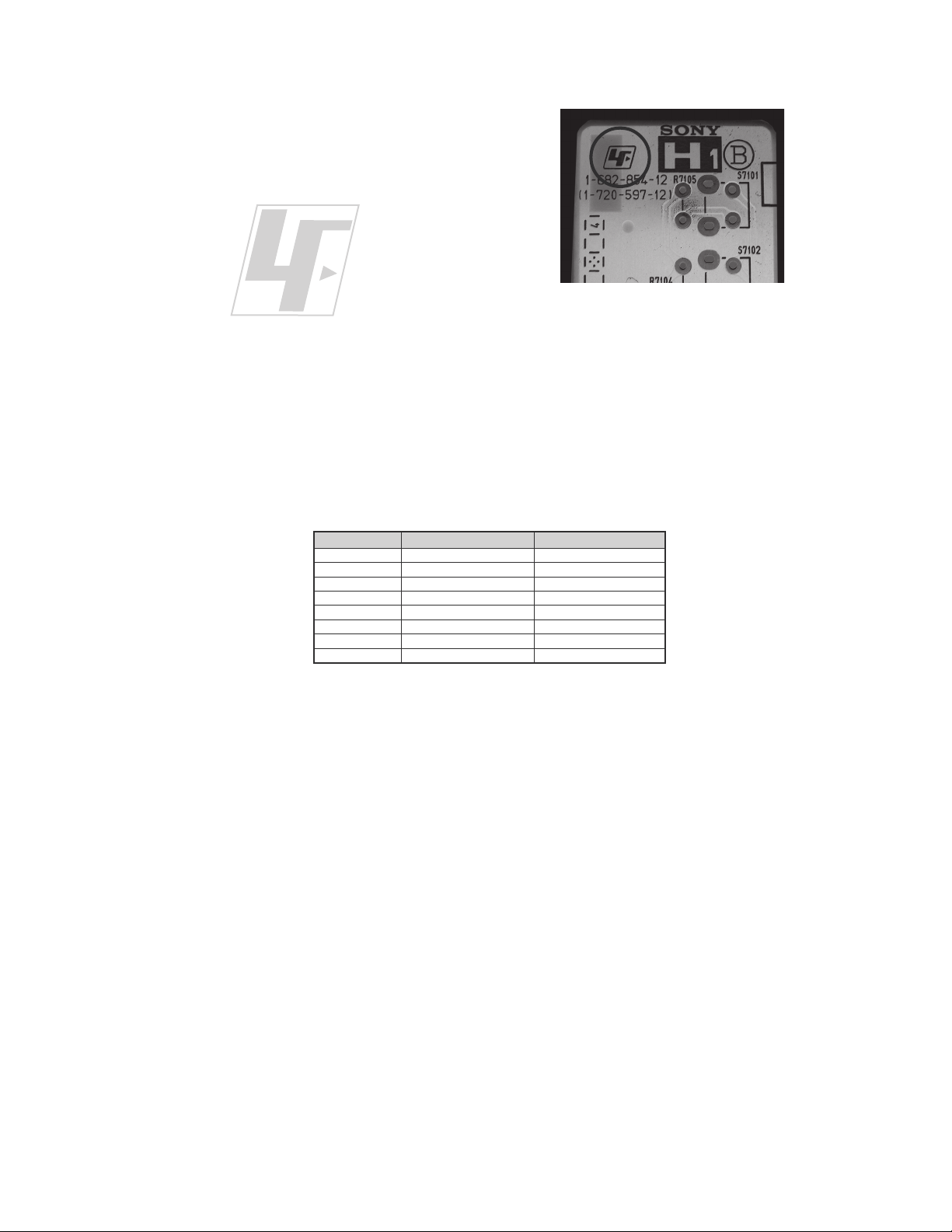
The circuit boards used in these models have been processed using
Lead Free Solder. The boards are identified by the LF logo located
close to the board designation e.g. H1 etc [ see example ]. The
servicing of these boards requires special precautions to be taken as
outlined below.
example
It is strongly recommended to use Lead Free Solder material in order to guarantee optimal quality of new solder joints.
Lead Free Solder is available under the following part numbers :
r e b m u n t r a P r e t e m a i D s k r a m e R
9 1 - 5 0 0 - 0 4 6 - 7m m 3 . 0g K 5 2 . 0
0 2 - 5 0 0 - 0 4 6 - 7m m 4 . 0g K 0 5 . 0
1 2 - 5 0 0 - 0 4 6 - 7m m 5 . 0g K 0 5 . 0
2 2 - 5 0 0 - 0 4 6 - 7m m 6 . 0g K 5 2 . 0
3 2 - 5 0 0 - 0 4 6 - 7m m 8 . 0g K 0 0 . 1
4 2 - 5 0 0 - 0 4 6 - 7m m 0 . 1g K 0 0 . 1
5 2 - 5 0 0 - 0 4 6 - 7m m 2 . 1g K 0 0 . 1
6 2 - 5 0 0 - 0 4 6 - 7m m 6 . 1g K 0 0 . 1
Due to the higher melting point of Lead Free Solder the soldering iron tip temperature needs to be set to 370 degrees centigrade.
This requires soldering equipment capable of accurate temperature control coupled with a good heat recovery characteristics.
KLV-32BX300/40BX400
4
SAFETY CHECK-OUT
To E
l
KLV-32BX300/40BX400
After correcting the original service problem, perform the following
safety checks before releasing the set to the customer:
1. Check the area of your repair for unsoldered or poorly soldered
connections. Check the entire board surface for solder splashes and
bridges.
2. Check the interboard wiring to ensure that no wires are “pinched” or
touching high-wattage resistors.
3. Check that all control knobs, shields, covers, ground straps, and
mounting hardware have been replaced. Be absolutely certain that
you have replaced all the insulators.
4. Look for unauthorized replacement parts, particularly transistors,
that were installed during a previous repair. Point them out to the
customer and recommend their replacement.
5. Look for parts which, though functioning, show obvious signs of
deterioration. Point them out to the customer and recommend their
replacement.
6. Check the line cords for cracks and abrasion. Recommend the
replacement of any such line cord to the customer.
7. Check the antenna terminals, metal trim, “metallized” knobs, screws,
and all other exposed metal parts for AC leakage. Check leakage as
described below.
The AC leakage from any exposed metal part to earth ground and
from all exposed metal parts to any exposed metal part having a
return to chassis, must not exceed 0.5 mA (500 microamperes).
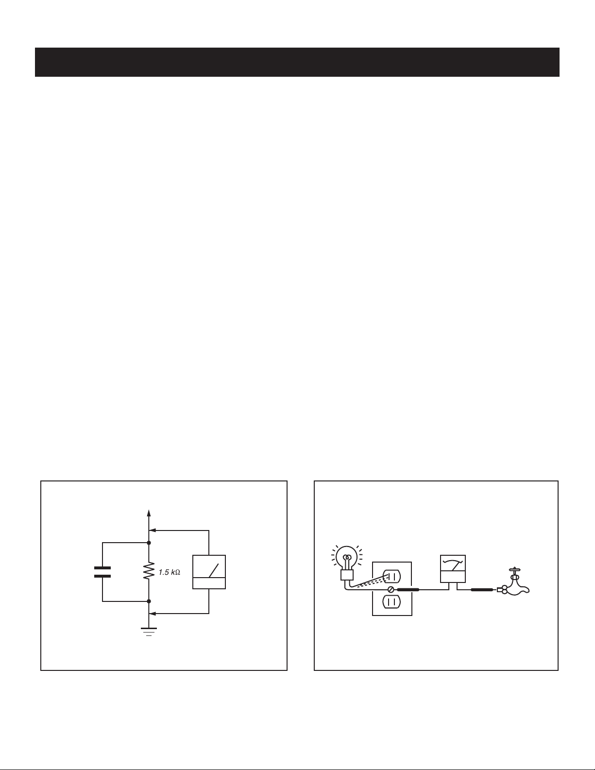
Leakage current can be measured by any one of three methods.
1. A commercial leakage tester, such as the Simpson 229 or RCA
WT-540A. Follow the manufacturers’ instructions to use these
instructions.
2. A battery-operated AC milliampmeter. The Data Precision 245
digital multimeter is suitable for this job.
3. Measuring the voltage drop across a resistor by means of a VOM
or battery-operated AC voltmeter. The “limit” indication is 0.75
V, so analog meters must have an accurate low voltage scale.
The Simpson’s 250 and Sanwa SH-63TRD are examples of
passive VOMs that are suitable. Nearly all battery-operated digital
multimeters that have a 2 VAC range are suitable (see Figure A).
How to Find a Good Earth Ground
A cold-water pipe is a guaranteed earth ground; the cover-plate
retaining screw on most AC outlet boxes is also at earth ground. If the
retaining screw is to be used as your earth ground, verify that it is at
ground by measuring the resistance between it and a cold-water pipe
with an ohmmeter. The reading should be zero ohms.
If a cold-water pipe is not accessible, connect a 60- to 100-watt
trouble- light (not a neon lamp) between the hot side of the receptacle
and the retaining screw. Try both slots, if necessary, to locate the hot
side on the line; the lamp should light at normal brilliance if the screw
is at ground potential (see Figure B).
Leakage Test
0.15 μF
Figure A. Using an AC voltmeter to check AC leakage. Figure B. Checking for earth ground.
xposed Meta
Parts on Set
Earth Ground
AC
Voltmeter
(0.75V)
Trouble Light
AC Outlet Box
Ohmmeter
Cold-water Pipe
KLV-32BX300/40BX400
5
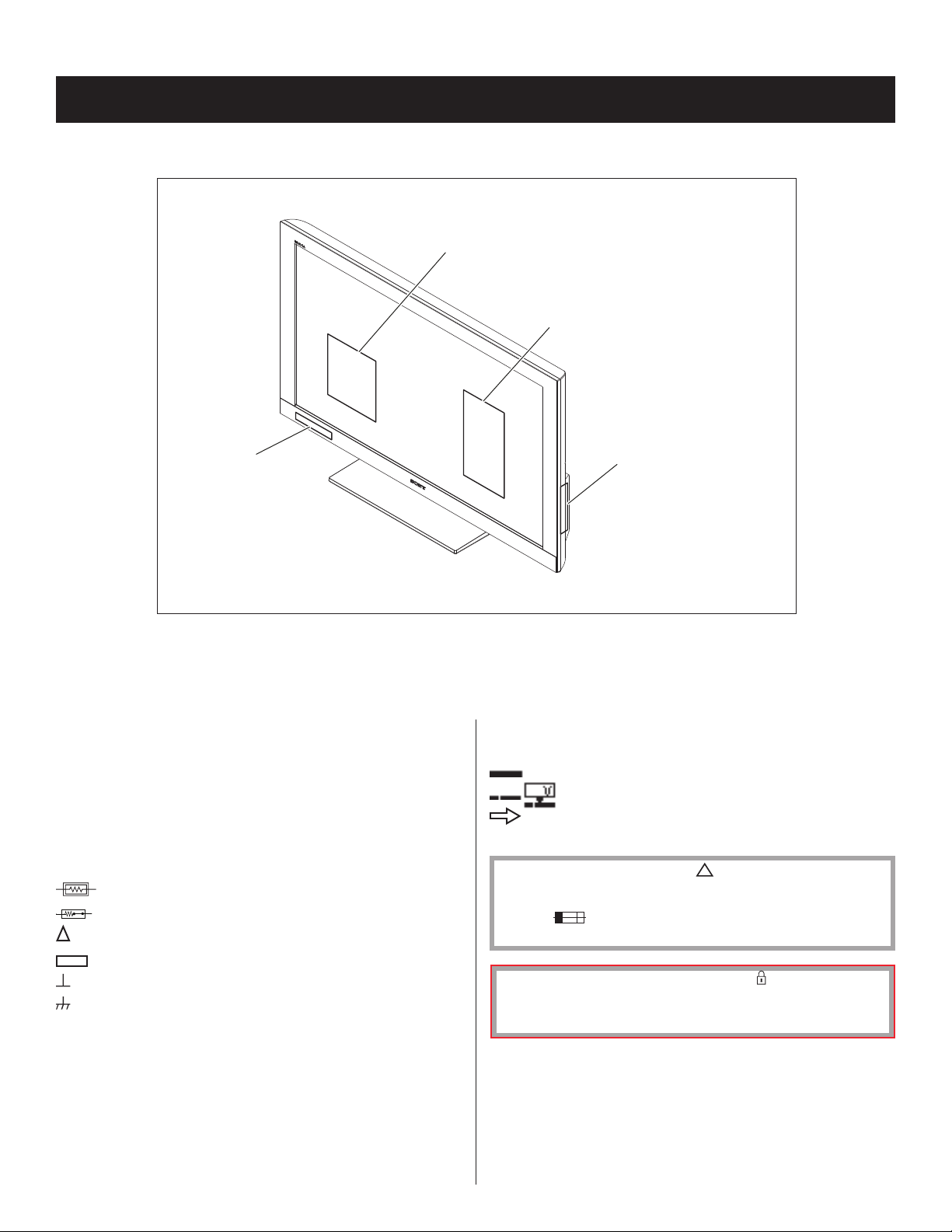
1-1. CIRCUIT BOARDS LOCATION
KLV-32BX300/40BX400
SECTION 1: DIAGRAMS
BAA
G2LE (KLV-32BX300 ONLY)
G2HE (KLV-40BX400 ONLY)
H2LR
1-2.
PRINTED WIRING BOARDS AND SCHEMATIC DIAGRAMS INFORMATION
All capacitors are in μF unless otherwise noted. pF : μμF 50WV or
less are not indicated except for electrolytics and tantalums.
All electrolytics are in 50V unless otherwise specifi ed.
All resistors are in ohms. k=1000, M=1000k
Indication of resistance, which does not have one for rating
electrical power, is as follows: Pitch : 5mm
Rating electrical power :
1
/
W in resistance, 1/
4
W and 1/
10
W in chip resistance.
16
1
/
4
: nonfl ammable resistor
: fusible resistor
: internal component
All voltages are in V.
S : Measurement impossibility.
: B+line.
: B-line. (Actual measured value may be different).
: signal path. (RF)
Circled numbers are waveform references.
W
The components identifi ed by shading and ! symbol are critical for safety. Replace
only with part number specifi ed.
The symbol indicates a fast operating fuse and is displayed on the component
side of the board. Replace only with fuse of the same rating as marked.
H2LS
: panel designation and adjustment for repair
: earth ground
: earth-chassis
All variable and adjustable resistors have characteristic curve B,
NOTE: The components identifi ed by a red outline and a mark contain confi dential
information. Specifi c instructions must be adhered to whenever these components
are repaired and/or replaced.
See Appendix A: Encryption Key Components in the back of this manual.
unless otherwise noted.
Readings are taken with a color-bar signal input.
Readings are taken with a 10M digital multimeter.
Voltages are DC with respect to ground unless otherwise noted.
Voltage variations may be noted due to normal production
tolerances.
KLV-32BX300/40BX400
6
KLV-32BX300/40BX400
REFERENCE INFORMATION
RESISTOR
: RN METAL FILM
: RC SOLID
: FPRD NONFLAMMABLE CARBON
: FUSE NONFLAMMABLE FUSIBLE
: RW NONFLAMMABLE WIREWOUND
: RS NONFLAMMABLE METAL OXIDE
: RB NONFLAMMABLE CEMENT
: ADJUSTMENT RESISTOR
COIL
: LF-8L MICRO INDUCTOR
CAPACITOR
: TA TANTALUM
: PS STYROL
: PP POLYPROPYLENE
: PT MYLAR
: MPS METALIZED POLYESTER
: MPP METALIZED POLYPROPYLENE
: ALB BIPOLAR
: ALT HIGH TEMPERATURE
: ALR HIGH RIPPLE
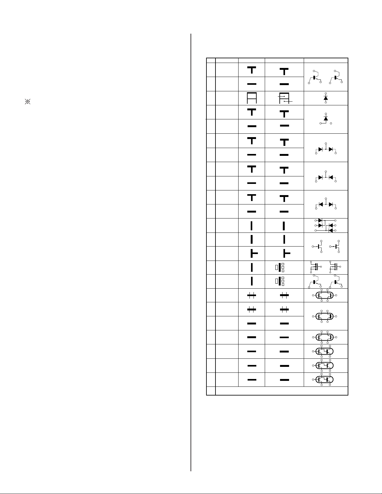
Terminal name of semiconductors in silk screen
printed circuit ( )
Device Printed symbol Terminal name
Transistor
1
Transistor
2
3
Diode
4
Diode
Diode
5
Diode
6
Diode
7
8
Diode
Diode
9
Diode
10
Diode
11
Diode
12
Transistor
13
(FET)
Transistor
14
(FET)
Transistor
15
(FET)
Transistor
16
Transistor
17
Transistor
18
Transistor
19
Transistor
20
Transistor
21
Transistor
22
Transistor
23
Discrete semiconductor
–
(Chip semiconductors that are not actually used are included.)
*
Collector
Base
Collector
Base
Cathode
Cathode
Anode
Cathode
Anode
Common
Anode
Common
Anode Cathode
Common
Anode
Common
Anode Anode
Common
Cathode
Common
Cathode
Anode
Anode
Cathode
Drain
Drain
B1 E1
C2
B2 C1E2
B2 E2
C1
B1 C2
E1
B2 E2
C1
B1 C2E1
B2 E2
C1
B1 C2E1
E2
B1 E1
C2
(B2)
E1
B1
C1
(B2)
E1
E2
C2
Emitter
Emitter
Anode
(NC)
(NC)
Cathode
Anode
Cathode
Cathode
Cathode
Anode
Anode
Source
Gate
Source
Gate
Source
Drain
Gate
Emitter
Collector
Base
C1(B2)
E2
C2
B1
C1
Circuit
D
G
D
S
B1
B1
B1
B1
B1
B1
D
G
S
S
D
G
C1
E1
C1
E1
E1
C1
E2
C1
C1
G
S
C2
B2
E2
C2
B2
E2
E2
B2
C2
C2C1(B2)
E2
E2E1(B2)
C2
C2E1(B2)
C2
Ver.1.6
KLV-32BX300/40BX400
7
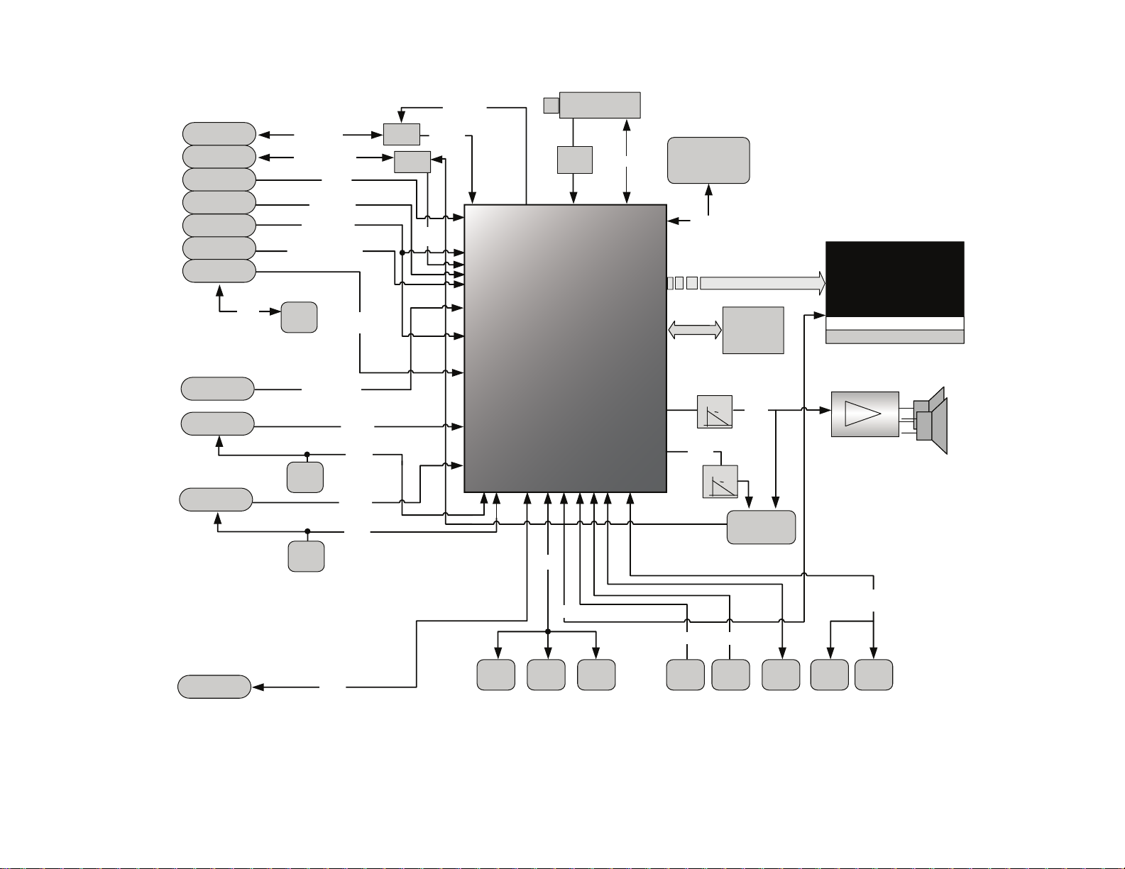
1-3. BLOCK DIAGRAM
FPL
FPL
O/I ortnoC
nI_FI
8835TM
AGB
SBVC
hc2 x tuO
CVBS
In x 4ch
Audio
In x 7ch
YUV
In x 2ch
RGB
In x 1ch
TMDS
In x 3ch
Audio
out x 2ch
Memory
I/F
Dual
Ch LVDS
tuO SBVC
WS
WS
nI
R/L
nI SBVC
7~0DDP
C2I uT
WAS
)zM83(
renuT
DNAN
HSALF
etyBM46
RETREVNI lanoitnevnoC
LFCC
LENAP
tib8
)AGXW(
tuo eniL
MWP
tiB61
MWP
2D0113APT
9772MJN
PMA
SCRIS
DEL
DEL
GATJ
letoH
TRAU
SCE
YBTS
0TRAU
SCRIS
C2I_M
BGR
tneibmA
rosnes
niaM
MVN
etyBK61
pmeT
rosneS
1BSU
2IMDH
DIDE
-D
/+D
0CDD
2IMDH
1IMDH
DIDE
2SDMT
2CDD
CCD
2IMDH/
CP
R/L
1IMDH
CP
DIDE
BGR
VH
R/L 3IMDH/CP
0SDMT
1 oediV
tuO NOM
noM/1 oedi
V
R/L
2 oediV
2 oediV
R/L
1 tnenopmoC
3oediV/
3oediV/1pmoC
R/L
CP
noM/1SBVC
R/L noM/1oediV
2SBVC
R/L 2oediV
3SBVC/1
vuY
R/L 3oediV/1pmoC
yromeM
2RDD
stib61xbM23
tib8 lennahC elgniS
C21_LENAP
KLV-32BX300/40BX400
KLV-32BX300/40BX400
8
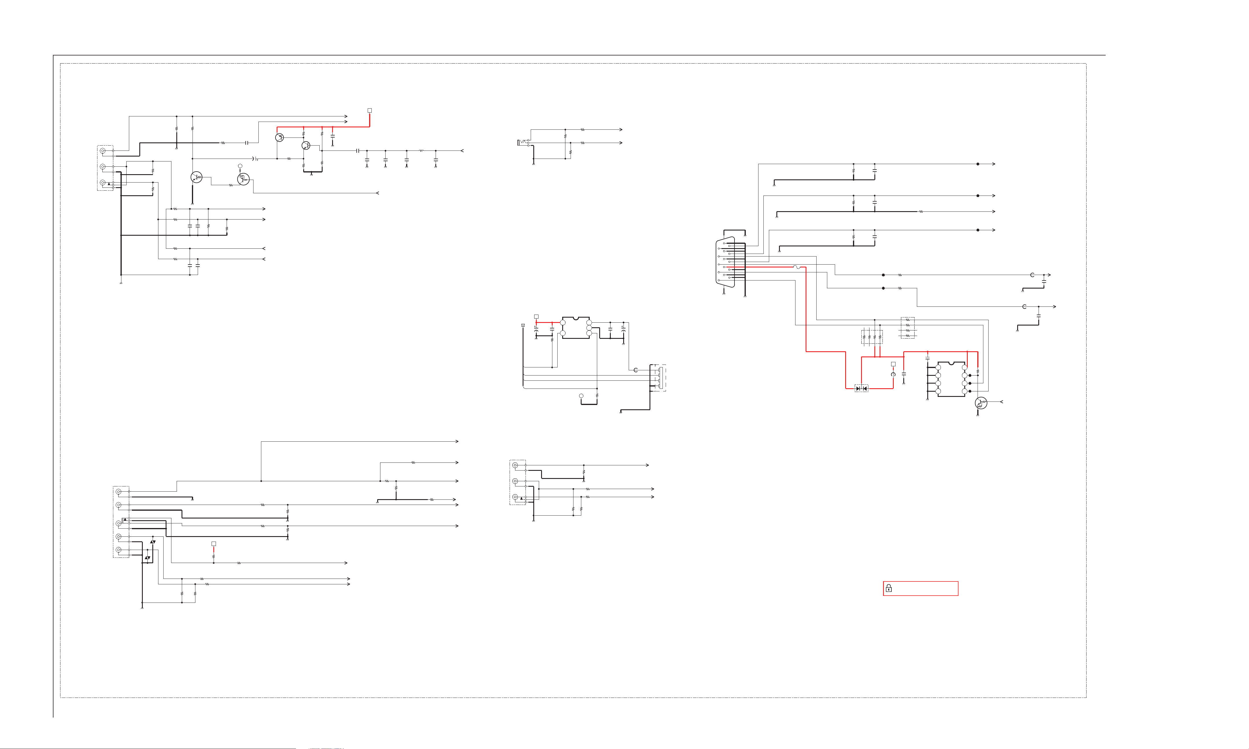
1-4. SCHEMATICS AND SUPPORTING INFORMATION
BAA BOARD SCHEMATIC DIAGRAM (1 OF 9)
1 | 2 | 3 | 4 | 5 | 6 | 7 | 8 | 9 | 10 | 11 | 12 | 13 | 14 | 15 | 16 | 17 | 18 | 19 | 20 | 21 | 22 | 23 | 24 | 25 |
A
—
B
220k
R2012
75
R2013
—
C
—
D
—
J2001
WHT
RED
YEL
R2004
1M
1/16W
R2005
1M
1/16W
GND_V
Q2001
RTAN140M-T111-1
R2008
2.2k
1/16W
R2009
2.2k
C2002
1/16W
0.001
GND_V
C2004
0.001
E
R2010
220
—
F
GND_A
R2011
220
C2003
0.001
C2005
0.001
—
G
—
H
—
I
R2014
1M
R2522
100
1/16W
CHIP
5%
R2020
100
1/16W
5%
R2016
+3.3V_MAIN
DRA5114E0L
1M
C2514
10V
X7R
1608
Q2002
KLV-32BX300/40BX400
+9V
V1_IO_CVBS1P+
V1_IO_CVBS0N-
470
R2023
Q2003
DSA500100L
1
C2007
220
V1_IN_L
009:2E
V1_IN_R
009:2E
LINE_OUT_L
005:12I;006:4F
LINE_OUT_R
005:12I
DSC500100L
180
R2022
Q2004
100
R2024
22k
R2026
GND_V
C2008
10k
R2027
0.1
GND_V
C2009
10
C2013
100p
GND_V
C2010
100p
VID_IO_SEL
GND_V GND_VGND_V
C2011
100p
L2001
1.8uH
C2012
100p
+_MON_OUT_IO_VDAC_OUT1
009:2E
J2201
009:16F
IO_USB
GND_A
+5V_MAIN
6.3V
100
C2513
USB_PWR
USB_DVM
USB_DVP
USB_OCP
GND_D
C2502
10k
R2502
16V
0.1
R2384
1M
1/16W
5%
R2385
1M
1/16W
5%
TPS2051BDBVR
IN
IC2501
OUT
GND
+3.3V_MAIN
R2372
2.2k
1/16W
R2373
2.2k
1/16W
/OCEN
10k
R2500
0.1
C2500
220
C2501
PC_HDMI_IN_L
PC_HDMI_IN_R
GND_D
GND_D
009:2E
009:2E
FB2500
0uH
1234
1
2
3
4
CN2500
4P
1112131415
CN2300
1617
678910
GND_D
JL2305
75
R2304
GND_V
75
R2305
GND_V
GND_D
12345
GND_V
GND_V
F2300
0.5A
R2306
75
10k
RB2000
D2300
BAV70
C2300
C2301
C2302
2143658
5p
5p
5p
JL2300
JL2301
7
0uH
FB2305
+5V_MAIN
R2311
R2312
JL2306
R2519
100
1/16W
CHIP
5%
22
22
100
RB2001
2
1
4
3
6
5
8
7
C2303
GND_V
0.1
C2306
0.1
GND_V
1
E0
2
E1
3
E2
4
VSS5SDA
K24C02C
IC2301
VCC
WP
SCL
8
JL2302
7
JL2303
6
JL2304
R2319
10k
JL2307
Q2300
DRC5114E0L
GND_V
PC_IO_RP+
PC_IO_GP+/SOG
PC_IO_COM
PC_IO_BP+
EDID_WP/PC_WP
FB2306
GND_V
0uH
GND_V
FB2307
0uH
5p
C2307
PC_IO_HSYNC
5p
C2308
PC_IO_VSYNC
—
J
—
K
—
L
—
M
—
N
J2200
V3_IO_CVBS3P+
009:2C
Y_IO_SOY0
Y_IO_Y0P+
009:2C
Y_IO_COM0
PB_IO_PB0P+
PR_IO_PR0P+
R2520
100
1/16W
CHIP
R2236
18
56
GRN
R2202
1M
GND_V
R2203
1M
R2204
2.2k
R2205
2.2k
+5V_MAIN
100k
R2248
R2249
4.7k
R2213
R2214
18
18
R2218
R2219
56
GND_V
56
GND_V
AV_COMP_SEL
009:11B
D1_IN_L
009:2E
D1_IN_R
009:2E
BLU
RED
WHT
RED
VD2201
VD2200
GND_A
R2238
GND_V
5%
R2521
100
J2100
YEL
WHT
RED
GND_A
R2103
1M
1/16W
5%
R2105
75
GND_V
R2104
1/16W
V2_IO_CVBS2P+
R2106
2.2k
1/16W
R2107
2.2k
1/16W
1M
5%
V2_IN_L
009:2E
V2_IN_R
009:2E
BAA 1/9
INPUT
—
O
—
A-1751-555-A <AZ1A> BAA-P1
P
KLV-32BX300/40BX400 9
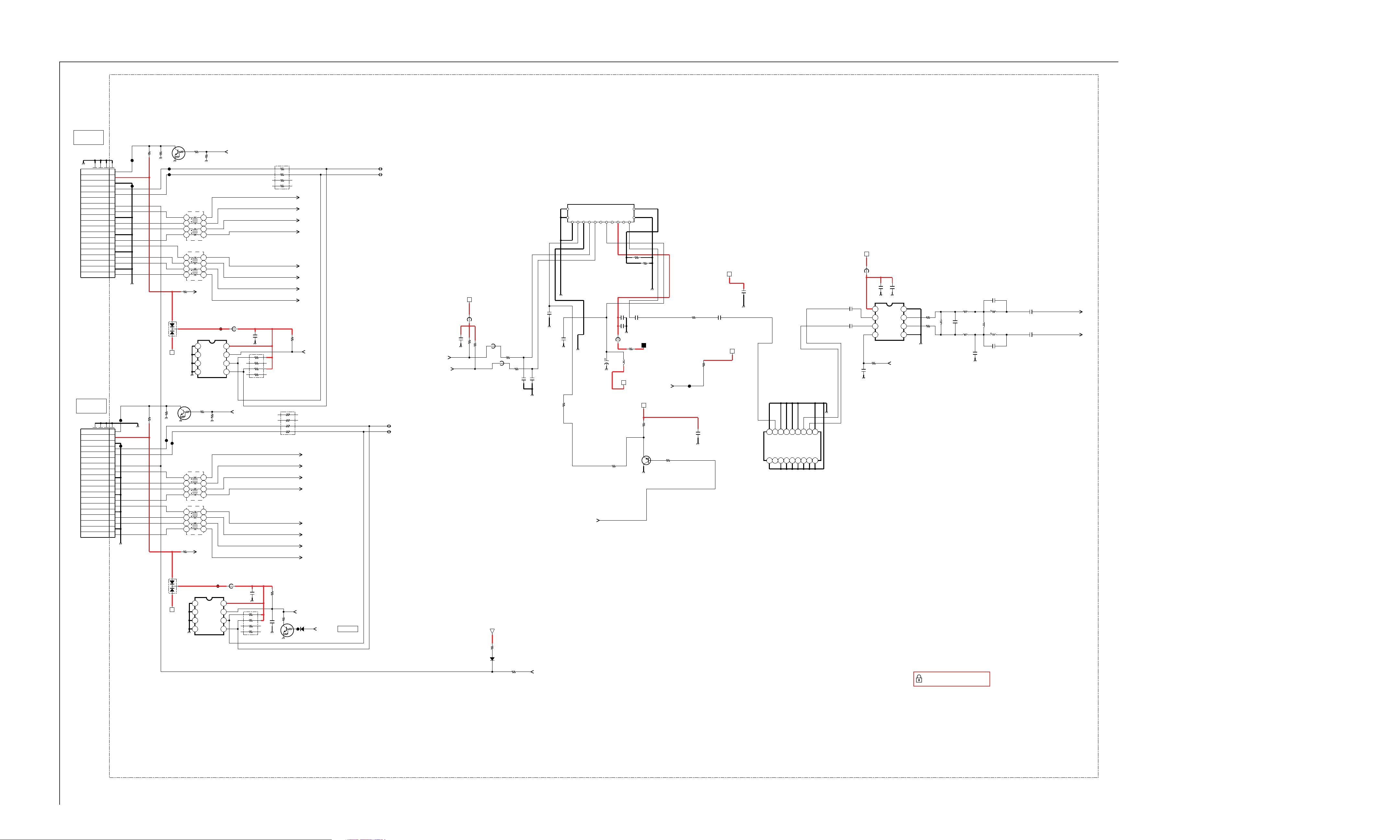
BAA BOARD SCHEMATIC DIAGRAM (2 OF 9)
1 | 2 | 3 | 4 | 5 | 6 | 7 | 8 | 9 | 10 | 11 | 12 | 13 | 14 | 15 | 16 | 17 | 18 | 19 | 20 | 21 | 22 | 23
A
—
KLV-32BX300/40BX400
B
—
C
—
D
—
E
—
F
—
G
—
H
—
I
—
J
—
K
HDMI_1
GND_D
CN2600
19P
HDMI_2
CN2601
19P
19HPD
18DDC +5V
17E
16DDC DAT
15DDC CLK
14NC
13CEC
12CLK-
11E
10CLK+
9D0-
8E
7D0+
6D1-
5E
4D1+
3D2-
2E
1D2+
JL2605
19HPD
18DDC +5V
17E
16DDC DAT
15DDC CLK
14NC
13CEC
12CLK-
11E
10CLK+
9D0-
8E
7D0+
6D1-
5E
4D1+
3D2-
2E
1D2+
JL2608
JL2600
GND_D
JL2603
GND_D
GND_D
R2600
R2601
Q2600
DRC5114E0L
R2603
100k
1k
GND_D
JL2601
JL2602
+5V_MAIN
R2604
100k
GND_D
1k
JL2606
GND_D
JL2607
1
2
3
4
1
2
3
4
R2657
1k
BAV70
D2601
DRC5114E0L
GND_D
1
2
3
4
1
2
3
4
R2658
1k
L2600
90ohm
L2601
90ohm
010:8H
GND_D
Q2601
L2602
90ohm
L2603
90ohm
010:8H
R2606
1k
PWR5V_0
4321
PWR5V_2
GND_D
5
6
7
8
5
6
7
8
A1
A0
A2
E SDA
R2607
1k
5
6
7
8
5
6
7
8
K24C02C
IC2602
GND_D
R2609
10k
VCC
SCL
R2610
10k
JL2604
WP
HDMI_HPD0
009:4B
FB2602
C2602
0uH
16V
HDMI_HPD2
009:4D
1005
8765
0.1
8
6
4
2
GND_D
*RB2605
22k
8
7
6
5
4
3
2
1
RB2601
100
7
5
3
1
RX2_CB
RX2_C
RX2_0B
RX2_0
RX2_1B
RX2_1
RX2_2B
RX2_2
7
5
3
1
*R2624
22k
RB2602
100
009:4A
009:4A
009:4B
009:4B
009:4B
009:4B
009:4B
009:4B
8
6
4
2
RX0_CB
RX0_C
RX0_0B
RX0_0
RX0_1B
RX0_1
RX0_2B
RX0_2
EDID_WP_B
RX2_CB
009:4C
RX2_C
009:4C
RX2_0B
009:4D
RX2_0
009:4C
RX2_1B
009:4D
RX2_1
009:4D
RX2_2B
009:4D
RX2_2
009:4D
HDMI_SDA0 009:4B
HDMI_SCL0 009:4B
HDMI_SDA2 009:4D
HDMI_SCL2 009:4D
SCL_TUNER
SDA_TUNER
0uH
FB1006
GND_C
+5V_MAIN
C1046
0.01
R1035
4.7k
R1036
4.7k
FB1007
0uH
FB1008
XX
TU1001
&
GND
N/C(AS)
SCL
SDA
MB
TUNING
RF AGC
N/C
IF OUT
N/C
N/C
NTSC
+5V_MAIN
R1037
0
R1038
0
Multi
220
C1011
0.01
25V
X7R
R1028
4.7k
+33V_TUNER
+5V_MAIN
DSA500100L
GND_C
GND_C
Q1007
SAW87_SW
R1030
100
009:11C
JL1000
R1013
1/16W
CHIP
47
R1057
GND_C
10k
1005
X7R
25V
0.01
C1030
GND_C
C1008
GND_C
C1009
FB1003
0uH
R1032
4.7k
1/16W
RN-CP
0.5%
50V
X7R
1
0.01
50V
GND_C
10uH
L1010
+5V_MAIN
F
R1056
C1000
0.01
GND_C
C1001
0.001
50V
X7R
R1002
GND_C
GND_C
0
RF_AGC
009:12B
C1006
16V
47
R1006
10
0uH
R1007
C1003
10
100p
GND_C
C1004
100p
C1017
4700p
50V
X7R
+5V_MAIN
+5V_MAIN
GND_C
1005
X7R
50V
0.001
C1018
Multi
&
123456 8
SF1001
NTSC
XX
0uH
FB1005
1005
X7R
25V
0.01
C1021
0.047
1005
GND_C
C1022
R1027
10k
C1019
0.01
25V
X7R
1005
C1020
0.01
25V
X7R
1005
GND_C
10911127131415161718
2012
X6S
6.3V
C1023
GND_C
GND_C
UPC3234GV-E1-A
IC1000
IF_AGC
009:2B
GND_D
0.39uH
L1008
C1040
39p
50V
CH
1005
L1009
220nH
L1005
220nH
C1039
39p
50V
CH
1005
C1042
0.01
25V
X7R
1005
C1043
0.01
25V
X7R
1005
IFOUT+
009:2A
IFOUT009:2A
10
L1004
0.39uH
L1006
50V
68p
C1051
0.39uH
L1003
0.39uH
XX
C1053
GND_C
R1033
100
1/16W
R1034
100
1/16W
—
L
—
M
—
N
—
O
+5V_MAIN
BAV70
D2602
GND_D
4321
K24C02C
IC2601
A1
A0
A2
E SDA
JL2609
FB2601
0uH
8765
VCC
WP
SCL
C2601
0.1
GND_D
8
6
4
2
*RB2606
22k
7
5
3
1
*R2622
22k
R2623
0.01
GND_D
0
R2628
GND_D
EDID_WP_B
Q2603
DRC5114E0L
JL2610
D2603
MA2SD320G8S0
EDID_WP/PC_WP
TO MTK
+3.3V_STBY
R2632
MA2SD320G8S0
27k
D2605
HDMI_CEC
R2667
33
009:4D
BAA 2/9
HDMI/TUNER
—
A-1751-555-A <AZ1A> BAA-P2
P
KLV-32BX300/40BX400 10
BAA BOARD SCHEMATIC DIAGRAM (3 OF 9)
1 | 2 | 3 | 4 | 5 | 6 | 7 | 8 | 9 | 10 | 11 | 12 | 13 | 14 | 15 | 16 | 17 | 18 | 19 | 20 | 21 | 22 |
A
—
B
—
C
—
D
—
009:5E
PWM_SP_OUT_L
009:5E
PWM_SP_OUT_R
PWM_SP_OUT_L
PWM_SP_OUT_R
E
—
F
—
JL4000
JL4001
R4000
33
1/16W
5%
R4001
33
1/16W
5%
007:3B;007:17I
POWER_ON
C4000
0.1
X7R
1005
C4001
0.1
X7R
1005
JL4002
JL4003
R4008
R4009
KLV-32BX300/40BX400
AU_VCC
X_SP_MUTE
009:8E
0
*R4104
R4101
1.5k
JL4011
0
GND_D
R4102
1.5k
0
R4100
1k
HP_DET
005:4J
X_AMP_FAULT
R4099
1k
R4031
33k
C4027
0.22
25V
X7R
1608
C4028
0.22
25V
X7R
1608
C4030
0.22
25V
X7R
1608
C4031
GND_A
0.22
25V
X7R
1608
*R4039
100k
C4032
1
R4043
100
R4042
100
C4033
100k
R4077
12
DZ2J03300L
D4008
1
SD
2
FAULT
3
LINP
4
LINN
5
GAIN0
6
GAIN1
7
AVCC
8
AGND
GND_DB
9
GVDD
10
PLIMIT
11
RINN
12
RINP
13
NC
PBTL
14
TPA3110D2PWPR
1
PVCCL
PVCCL
OUTPL
OUTNL
OUTNR
OUTPR
PVCCR
PVCCR
IC4002
BSPL
PGND
BSNL
BSNR
PGND
BSPR
12
29GND
28
27
26
25
24
23
22
21
20
19
18
17
16
15
C4037
0.22
25V
X7R
1608
C4038
0.22
C4039
0.22
C4040
0.22
C4041
0.001
50V
X7R
1005
C4042
0.001
R4049
10
R4050
10
R4051
10
R4052
12
L4004
C4043
0.1
25V
X7R
1608
C4045
0.001
C4046
0.001
C4047
0.001
C4048
0.001
10
C4044
0.1
C4049
10
16V
C4050
16V
C4015
16V
C4017
10
16V
GND_DB
C4016
10
10
FB4009
0uH
FB4010
0uH
10
16V
C4018
10
16V
15uH
12
L4005
15uH
12
L4006
15uH
12
L4007
15uH
C4059
0.47
C4060
0.47
C4061
0.47
C4062
0.47
GND_DB
GND_DB
1
L+
2
L-
3
R-
4
R+
CN4000
4P
G
—
H
—
I
—
J
—
ALL_MUTE
005:8C;005:9J
JL4016
BAV70
D4001
Q4008
DSA500100L
Q4009
DSA500100L
GND_D
R4083
1/16W
JL4017
R4082
47k
1/16W
R4080
47k
R4112
D4003
BAT54J
AU_VCC
JL4018
D4002
1k
DI BAT54J
R4081
1k
1/16W
CHIP
5%
1005
+3.3V_MAIN
+9V
AUDIO_12V
24V
4A
F4001
47k
R4061
0
R4018
0
R40190R4020
GND_D
JL4014
JL4015
HP_OUT_L
003:10C
HP_OUT_R
003:10C
1k
C4066
10
6.3V
C4065
10
6.3V
K
—
L
—
M
—
N
—
009:5E
PWM_LINE_OUT_L
009:6E
PWM_LINE_OUT_R
009:12A
X_AUDIO_PROT
005:8D
X_AMP_FAULT
X_LINE_MUTE
006:4F;009:10F
JL4004
JL4005
PWM_LINE_OUT_L
PWM_LINE_OUT_R
R4016
1/16W
5%
R4017
1/16W
5%
NJM2779VC3-TE2
16V
1
C4075
C4074
16V
1
R4095
1k
33
33
C4013
C4014
0.022
0.022
25V
25V
X7R
X7R
1005
1005
C4071
C4070
1
1
GND_A
DET_A
DET_B
GND
HPMT_I
LINE_MT_I
HP_L_IN
HP_R_IN
GND
LINE_L_IN
10987654321
LNE_R_INLINE_MT_O
IC4003
X_PROT_O
FAULT_I
HP_MT_O
LINE_L
LINE_R
HP_L
HP_R
20
GND
19 18 17 16 15 14 13 12 11
VEF
C4067
10
Q4004
DRC5114E0L
005:1F;005:8C
Q4002
DRA5114T0L
ALL_MUTE
Q4003
DRA5114T0L
C4034
1
25V
X7R
2012
12
C4035
1
25V
2012
X7R
VID_IO_SEL
003:6B;009:12A
D4007
DA2J10100L
R4047
1/16W
1005
R4048
1k
1/16W
1005
1k
Q4007
RT3X99M
GND_A
JL4012
JL4013
HP_GND
003:10C
LINE_OUT_L
003:4C;006:4F
LINE_OUT_R
003:4C
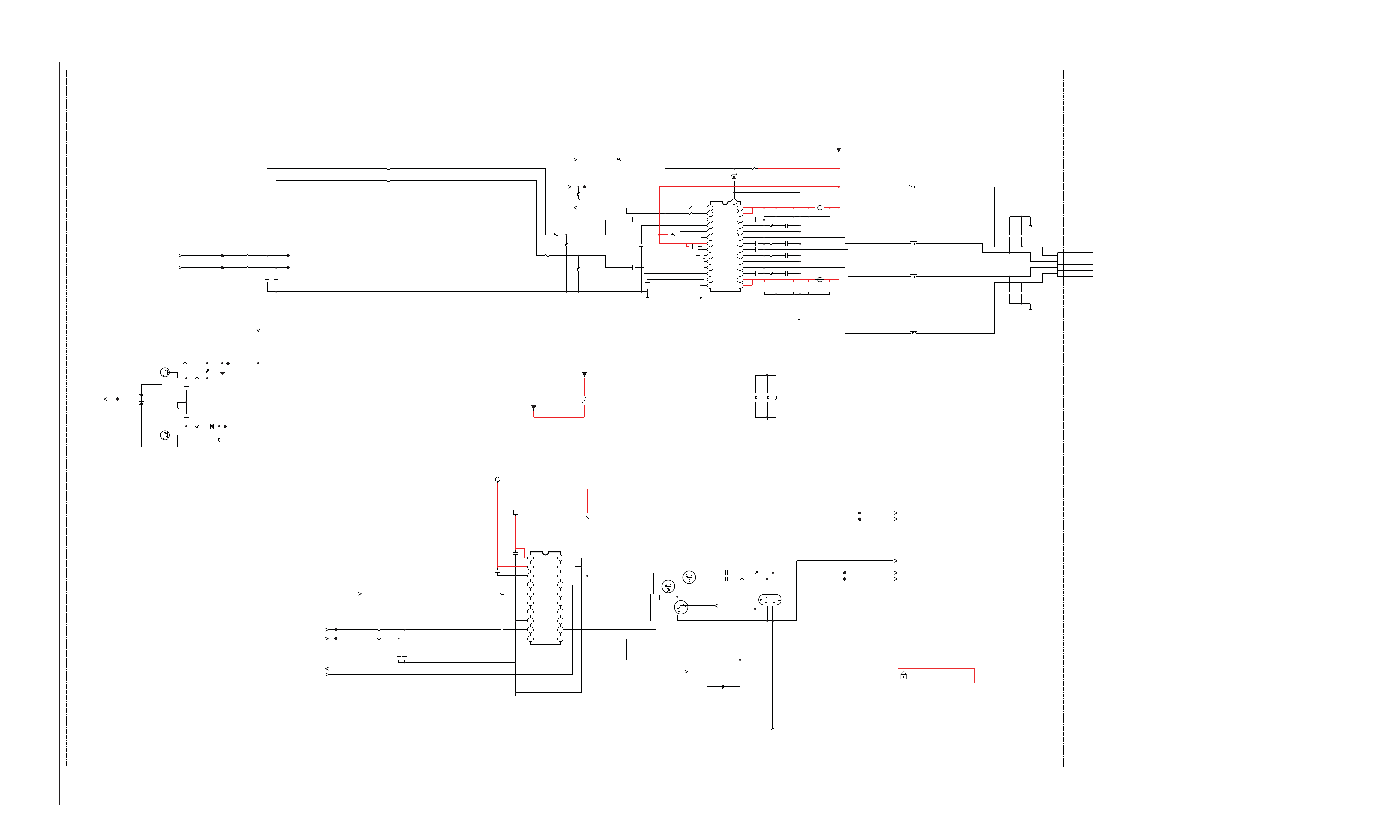
BAA 3/9
AUDIO
O
—
A-1751-555-A <AZ1A> BAA-P1
P
KLV-32BX300/40BX400 11
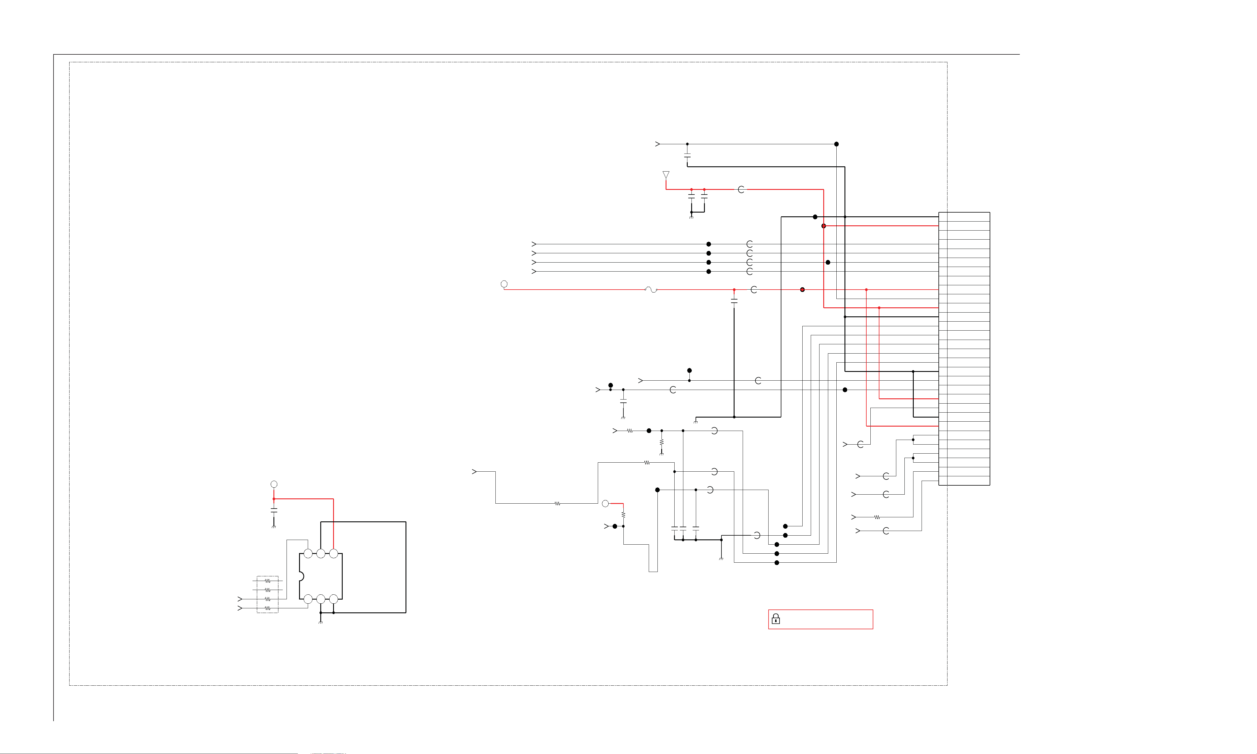
BAA BOARD SCHEMATIC DIAGRAM (4 OF 9)
1 | 2 | 3 | 4 | 5 | 6 | 7 | 8 | 9 | 10 | 11 | 12 | 13 | 14 | 15 | 16 | 17 | 18 | 19 | 20 | 21 | 22 | 23 |
A
—
B
KLV-32BX300/40BX400
—
C
—
D
—
E
—
F
—
G
—
H
—
I
—
J
—
K
—
L
—
M
—
M_SDA
M_SCL
+3.3V_MAIN
1005
X7R
16V
0.1
C5200
GND_D
47
RB5600
1
3
5
7
SIRCS
+3.3V_STBY
STBY_LED
TIMER_LED
POWER_LED
PICTURE_OFF_LED
+3.3V_MAIN
F5600
0.5A
JL5600
KEY2
BACKLIGHT
DIMMER_PWM
009:11G;009:13D
R5627
0
456
A0
SDA
2
SCL
4
6
8
GND
123
MM3285CNRE
IC5200
A1 VDD
+3.3V_MAIN
PANEL_DET
GND_D
JL5601
KEY1
C5606
R5615
2.2k
R5616
10k
0.01
25V
JL5602
1005
0
*R5611
CHIP
JL5603
GND_D
FB5600
0uH
27k
R5625
C5607
220p
50V
1005
X7R
50V
220p
C5610
C5611
2.2
JL5604
C5609
GND_D
GND_D
4.7
10V
JL5606
JL5607
JL5608
JL5609
FB5601
0uH
FB5602
0uH
C5613
0.01
25V
X7R
1005
1005
X7R
50V
0.001
C5614
GND_D
1005
CH
50V
100p
C5617
FB5603
0uH
FB5604
0uH
FB5620
0uH
FB5623
FB5611
0uH
0uH
FB5624
0uH
FB5615
0uH
FB5621
0uH
FB5622
0uH
JL5615
JL5616
JL5612
JL5613
JL5614
JL5618
JL5619
JL5617
006:7B;007:3B;007:14H;009:9A;009:9A;009:12A;012:9G
JL5621
JL5620
JL5622
POWER3
009:11B;012:7J
M_SDA
006:4H;009:3I;009:10C
M_SCL
006:4H;009:3I;009:10C
AC_OFF_DET
011:2B;012:9G
HFR_HSYNC
FB5619
0uH
FB5616
0uH
FB5617
0uH
R5629
100
FB5618
0uH
1
GND
2
STBY3.3V
3
MOTION_SENSOR
4
STBY_LED
5
ON_TIMER
6
PWR/RESERVE
7
PICTURE_OFF
8
NC
9
VD3.3V
10
SIRCS
11
STBY3.3V
12
GND
13
NC
14
GND
15
BL_ERROR
16
BACKLIGHT
17
DIMMER_PWM
18
GND
19
KEY1/POWER_INT
20
KEY2
21
STBY3.3V_CL
22
T-con_ON
23
GND
24
MAIN_DET
25
SDA_CL
26
SDA_RBG
27
SCL_CL
28
SCL_RGB
29
AC_OFF_DET
30
INV_Hsync
CN5600
30P
N
GND_D
—
BAA 4/9
MICON
O
—
A-1751-555-A <AZ1A> BAA-P4
P
KLV-32BX300/40BX400 12
 Loading...