

Page 1
SERVICE MANUAL
LG-3
CHASSIS
MODEL COMMANDER DEST. CHASSIS NO.
–––––– –––––––––––– ––––– –––––––––––
KF-WE42A1 RM-1022 E
KF-WE50A1 RM-1022 E
KF-WS60A1 RM-1022 E
MODEL COMMANDER DEST. CHASSIS NO.
–––––– –––––––––––– ––––– –––––––––––
VIDEO
HD/DVD
CENTER
WEGA
FREEZE
DRC-MF
SP
THEATRE
V CENTER
A/B
MENU
R
O
P
G
N
I
+
W
T
PROG
INDEX
-
T
W
G
I
O
N
R
P
1
2
3
4
5
6
7
8
9
0
PROG
OPTION RESET
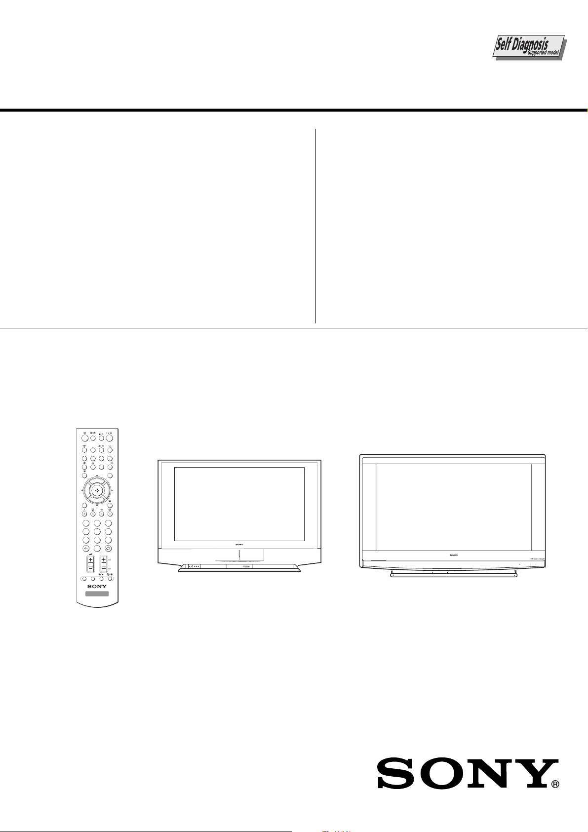
TV
RM-1022 KF-WE42A1/WE50A1 KF-WS60A1
PRO
STD/DUO
LCD PROJECTION TV
Page 2
KF-WE42A1/WE50A1/WS60A1
RM-1022 RM-1022 RM-1022
Specifications
Projection system 3 LCD Panels, 1 lens projection system
LCD Panel 0.87 inch TFT LCD panel Approx. 3.28 million dots (1,042,168 pixels)
Projection lenses High performance, large-diameter highbrid lens F2.4
Lamp KF-WE42 (A1)/KF-WE50 (A1): UHP lamp, 100 W, XL-2100C
KF-WS60 ( A1): UHP lamp, 120 W, XL-2300C
Screen size KF-WE42 (A1): 42 inches (1052 mm)
KF-WE50 (A1): 50 inches (1255 mm)
KF-WS60 (A1): 60 inches (1511 mm)
Television system B/G, I, D/K, M
Color system PAL, PAL 60, SECAM, NTSC4.43, NTSC3.58
Stereo/Bilingual system NICAM Stereo/Bilingual B/G, I, D/K; A2 stereo/Bilingual (German) B/G
Channel coverage B/G VHF: E2 to E12, UHF: E21 to E69, CATV: S01 to S03, S1 to S41
I UHF: B21 to B68, CATV: S01 to S03, S1 to S41
D/K VHF: C1 to C12, R1 to R12, UHF: C13 to C57, R21 to R60,
CATV: S01 to S03, S1 to S41, Z1 to Z39
M VHF: A2 to A13, UHF: A14 to A79, CATV: A-8 to A-2, A to W+4, W+6 to W+84
8 (Antenna) 75-ohm external terminal for VHF/UHF
Audio output (Speaker) 5 W + 5 W, 20 W (Woofer)
Number of terminal (Video) Input: 4 Phono jacks; 1 Vp-p, 75 ohms unbalanced, sync
Output: 1 negative
(Audio) Input: 6 Phono jacks; 500 mVrms (100% modulation)
Output: 1 Impedance: 47 kiloohms
Input: 4 Y: 1 Vp-p, 75 ohms, unbalanced, sync negative
(S Video) C: 0.286 Vp-p (Burst signal), 75 ohms
Input: 2 Phono jacks
(Component Y: 1 Vp-p, 75 ohms unbalanced, sync negative
Video) PB/CB: 0.7 Vp-p, 75 ohms
PR/CR: 0.7 Vp-p, 75 ohms
Audio: 500 mVrms
Input: 1 120 W max., 8 ohms
(Center
Speaker)
i
(Headphones)
Power requirements 220-240 V AC, 50/60 Hz
Power consumption In use KF-WE42 (A1)/KF-WE50 (A1): 210 W
In standby Less Than 1 W
Dimensions (W/h/d) KF-WE42 (S1, A1): 1200 x 818 x 339 mm
KF-WE50 (S1, A1): 1376 x 927 x 403 mm
KF-WS60 (S1, A1): 1574 x 1005 x 518 mm
Mass KF-WE42 (S1, A1): 32 kg
KF-WE50 (S1, A1): 38 kg
KF-WS60 (S1, A1): 50 kg
Output: 1 Stereo minijack
KF-WS60 (A1): 230 W
Design and specifications are subject to change without notice.
– 2 –
Page 3

KF-WE42A1/WE50A1/WS60A1
RM-1022 RM-1022 RM-1022
TABLE OF CONTENTS
Section Title Page
–––––– –––– ––––
SHORT CIRCUIT THE ANODE OF THE PICTURE TUBE AND THE
(CAUTION)
ANODE CAP TO THE METAL CHASSIS, CRT SHIELD, OR CARBON PAINTED ON THE CRT, AFTER REMOVING THE ANODE.
WARNING!!
AN ISOLATION TRANSFORMER SHOULD BE USED DURING
ANY SERVICE TO AVOID POSSIBLE SHOCK HAZARD, BECAUSE OF LIVE CHASSIS.
THE CHASSIS OF THIS RECElVER IS DIRECTLY CONNECTED
TO THE AC POWER LINE.
SAFETY-RELATED COMPONENT WARNING!!
COMPONENTS IDENTIFIED BY SHADING AND MARK ! ON
THE SCHEMATIC DIAGRAMS, EXPLODED VIEWS AND IN THE
PAR TS LIST ARE CRITICAL TO SAFE OPERATION. REPLACE
THESECOMPONENTS WITH SONY PARTS WHOSE PART NUMBERS APPEAR AS SHOWN IN THIS MANUAL OR IN SUPPLEMENTS PUBLISHED BY SONY. CIRCUIT ADJUSTMENTS THAT
ARE CRITICAL TO SAFEOPERATION ARE IDENTIFIED IN THIS
MANUAL. FOLLOW THESE PROCEDURES WHENEVER CRITICAL COMPONENTS ARE REPLACED OR IMPROPER OPERATION IS SUSPECTED.
1. SELF DIAGNOSIS FUNCTION ................................... 5
2. DISASSEMBLY
2-1. REAR COVER ............................................................ 9
2-2. CHASSIS PILLER ASSEMBLY
(WE42A1/WE50A1) ................................................... 9
2-3. OU BRACKET (WS60A1) ......................................... 9
2-4. SERVICE POSITION ............................................... 10
2-5. CHASSIS ASSEMBLY, OPTICS UNIT
(WE42A1/WE50A1) ................................................. 10
2-6. CHASSIS ASSEMBLY, FAN BRACKET (CHASSIS)
WITH DC FAN (WS60A1) ....................................... 10
2-7. OPTICS UNIT, FAN DUCT, T BOARD
(WS60A1) ................................................................. 11
2-8. WOOFER BLOCK ASSEMBLY
(WE42A1/WE50A1) ................................................. 11
2-9. WOOFER BLOCK ASSEMBLY
(WS60A1) ................................................................. 12
2-10. UG BOARD .............................................................. 12
2-11. B BLOCK ASSEMBLY ............................................ 13
2-12. F BOARD .................................................................. 13
2-13. KD BOARD .............................................................. 14
2-14. AG AND G1 BOARDS ............................................ 14
2-15. G2 AND H4 (WS60A1) BOARDS ........................... 15
2-16. POWER SUPPLY BLOCK ....................................... 15
2-17. T BOARD (WE42A1/WE50A1) .............................. 16
2-18. H3 BOARD (WE42A1) ............................................ 16
2-19. FRONT COVER ASSEMBLY
(WE42A1/WE50A1) ................................................. 16
2-20. HMG AND H3 BOARDS (WE50A1) ...................... 16
2-21. H2 BOARD (WE42A1/WE50A1) ............................ 17
2-22. HMG BOARD (WE42A1) ........................................ 17
2-23. H1 BOARD (WE42A1/WE50A1) ............................ 17
2-24. HMG BOARD (WS60A1) ........................................ 18
2-25. H1, H2 AND H3 BOARDS (WS60A1) .................... 18
2-26. SCREEN MIRROR BLOCK ASSEMBLY
(WE42A1/WE50A1) ................................................. 19
2-27. SCREEN MIRROR BLOCK ASSEMBLY
(WS60A1) ................................................................. 19
3. ELECTRICAL ADJUSTMENTS
3-1. ELECTRICAL ADJUSTMENT BY REMOTE
COMMANDER ........................................................ 20
3-2. To Read Lamp and Panel Time ................................. 22
3-3. Test Reset .................................................................. 22
3-4 LA-3 H/V Center Confirmaition and Adjustment ..... 22
– 3 –
Page 4

KF-WE42A1/WE50A1/WS60A1
RM-1022 RM-1022 RM-1022
Section Title Page
–––––– –––– ––––
4. DIAGRAMS
4-1. BLOCK DIAGRAM (1) ........................................... 23
BLOCK DIAGRAM (2) ........................................... 25
BLOCK DIAGRAM (3) ........................................... 27
BLOCK DIAGRAM (4) ........................................... 29
BLOCK DIAGRAM (5) ........................................... 31
BLOCK DIAGRAM (6) ........................................... 33
BLOCK DIAGRAM (7) ........................................... 35
BLOCK DIAGRAM (8) ........................................... 37
4-2. FRAME SCHEMATIC DIAGRAM .............................. 39
4-3. CIRCUIT BOARDS LOCATION ................................. 43
4-4. SCHEMATIC DIAGRAMS .......................................... 43
(1) Schematic Diagram of AG (1/5) Board ............. 45
(2) Schematic Diagram of AG (2/5) Board ............ 47
(3) Schematic Diagram of AG (3/5) Board ............ 49
(4) Schematic Diagram of AG (4/5) Board ............ 51
(5) Schematic Diagram of AG (5/5) Board ............ 53
(6) Schematic Diagram of B (1/6) Board ............... 55
(7) Schematic Diagram of B (2/6) Board ............... 57
(8) Schematic Diagram of B (3/6) Board ............... 59
(9) Schematic Diagram of B (4/6) Board ............... 61
(10) Schematic Diagram of B (5/6) Board ............... 63
(11) Schematic Diagram of B (6/6) Board ............... 65
(12) Schematic Diagram of C (1/3) Board ............... 67
(13) Schematic Diagram of C (2/3) Board ............... 69
(14) Schematic Diagram of C (3/3) Board ............... 71
(15) Schematic Diagram of F Board ......................... 73
(16) Schematic Diagram of G1 (1/2) Board ............. 75
(17) Schematic Diagram of G1 (2/2) Board ............. 77
(18) Schematic Diagram of G2 (1/4) Board ............. 79
(19) Schematic Diagram of G2 (2/4) Board ............. 81
(20) Schematic Diagram of G2 (3/4) Board ............. 83
(21) Schematic Diagram of G2 (4/4) Board ............. 85
(22) Schematic Diagram of WS60S1
H1, H2, H3, H4 Boards ...................................... 87
(23) Schematic Diagram of T, WE42A1/WE50A1
H1, H2, H3 Boards ............................................. 89
(24) Schematic Diagram of WE42A1/WE50A1
HMG Board ........................................................ 91
(25) Schematic Diagram of WE42A1/WE50A1
HMG Board ........................................................ 93
(26) Schematic Diagram of KD (1/2) Board ............. 95
(27) Schematic Diagram of KD (2/2) Board ............. 97
(28) Schematic Diagram of MS2C (1/3) Board ........ 99
(29) Schematic Diagram of MS2C (2/3) Board ...... 101
(30) Schematic Diagram of MS2C (3/3) Board ...... 103
(31) Schematic Diagram of UG (1/2) Board ........... 105
(32) Schematic Diagram of UG (2/2) Board ........... 107
Section Title Page
–––––– –––– ––––
4-5. PRINTED WIRING BOARDS.................................... 109
(1) AG Board (Side A) .......................................... 109
(2) AG Board (Side B) .......................................... 111
(3) B Board (Side A) ............................................. 113
(4) B Board (Side B) ............................................. 115
(5) C Board (Side A) ............................................. 117
(6) C Board (Side B) ............................................. 119
(7) F Board ............................................................ 121
(8) G1 Board (Side A) ........................................... 123
(9) G1 Board (Side B) ........................................... 125
(10) G2 Board (Side A) ........................................... 127
(11) G2 Board (Side B) ........................................... 129
(12) WE42A1, WE50A1
H1, H2, H3, HMG Boards .............................. 131
(13) WS60A1 H1, H2, H3, HMG Boards ............... 133
(14) KD Board ......................................................... 135
(15) MS2C Board .................................................... 137
(16) T Board ............................................................ 137
(17) UG Board ......................................................... 139
4-6. SEMICONDUCTORS ................................................. 141
5. EXPLODED VIEWS
5-1. KF-WE42A1/WE50A1
SCREEN MIRROR BLOCK, COVER ................... 143
5-2. KF-WE42A1/WE50A1 BOTTOM BLOCK .......... 144
5-3. KF-WS60A1
SCREEN MIRROR BLOCK, COVER ................... 145
5-4. KF-WS60A1 BOTTOM BLOCK .......................... 146
5-5. MAIN BRACKET-1 ............................................... 147
5-6. MAIN BRACKET-2 ............................................... 148
5-7. OPTICS UNIT BLOCK .......................................... 149
6. ELECTRICAL PARTS LIST..................................... 150
• AG Board .......................................................................... 150
• B Board ............................................................................. 155
• F Board ............................................................................. 155
• G1 Board ........................................................................... 156
• G2 Board ........................................................................... 158
• H1 Board ........................................................................... 158
• H2 Board ........................................................................... 158
• H3 Board ........................................................................... 159
• H4 Board ........................................................................... 160
• HMG Board ...................................................................... 160
• KD Board .......................................................................... 162
• MS2C Board ..................................................................... 165
• T Board ............................................................................. 165
• UG Board .......................................................................... 165
APPENDIX ........................................................................... 170
– 4 –
Page 5

KF-WE42A1/WE50A1/WS60A1
SECTION 1
RM-1022 RM-1022 RM-1022
SELF DIAGNOSIS FUNCTION
1. Summary of Self-Diagnosis Function
• This device has a self-diagnosis function.
• In case of failure, the POWER/STANDBY or LAMP LED blinks or lights to assist service.
It is possible to specify the cause of the failure by the number of blink or the LED itself.
The following list shows the interpretation of those LED related information.
• For the failure hard to be reproduced, its record is stored at the internal NVM.
The record can be displayed with the remote commander to specify the cause of the failure.
2. Diagnosis and probable cause of Failure
• In case of failure, the POWER/STANDBY or LAMP LED blinks or lights to indicate the following diagnosis.
If two or more failures occurred at one time, the one occurred first will be indicated.
If they occurred simultaneously, the one corresponds to the fewer times of blink will be indicated.
• All the failure records listed below can be displayed on the screen.
“ 0 ” will be displayed when there is no failure record.
Diagnosis Number of blink of Probable Cause Problem
STANDBY or LAMP
LED
Lamp cover error 3 times
Fan error 4 times - Fan connector is not seated - No picture/No sound
Temp error 4 times - IIC-E line - No picture/No sound
Lamp driver error 5 times - Lamp driver defect - No picture/No sound
Low B error 6 times
Audio error 7 times (F4702, F4703, F4704 on KD) - No picture/No sound
D-OVP error 8 times - Overvoltage of +3.3V or - No picture/No sound
Lamp error LAMP-LED is ON. - Lamp is dead - No picture/No sound
- Lamp cover is not - No picture/No sound
fastened securely.
- Fan 1-4 Power is no
supplied. (G2 board)
securely.
- Fan caught wires or
harnesses.
- Internal temperature is too
high.
connector (WE: H3 board,
WF/XS : H4) is not seated
properly.
- No “DD 6V” output (G1) - No picture/No sound
- ”PROT” is high (F)
-Short-circuit of Audio
power supply line (KD, G1)
- Blowout of a fuse
- IC failure
(IC4703, IC4708, IC4710 on
+2.5V (A, B board)
– 5 –
Page 6
KF-WE42A1/WE50A1/WS60A1
RM-1022 RM-1022 RM-1022
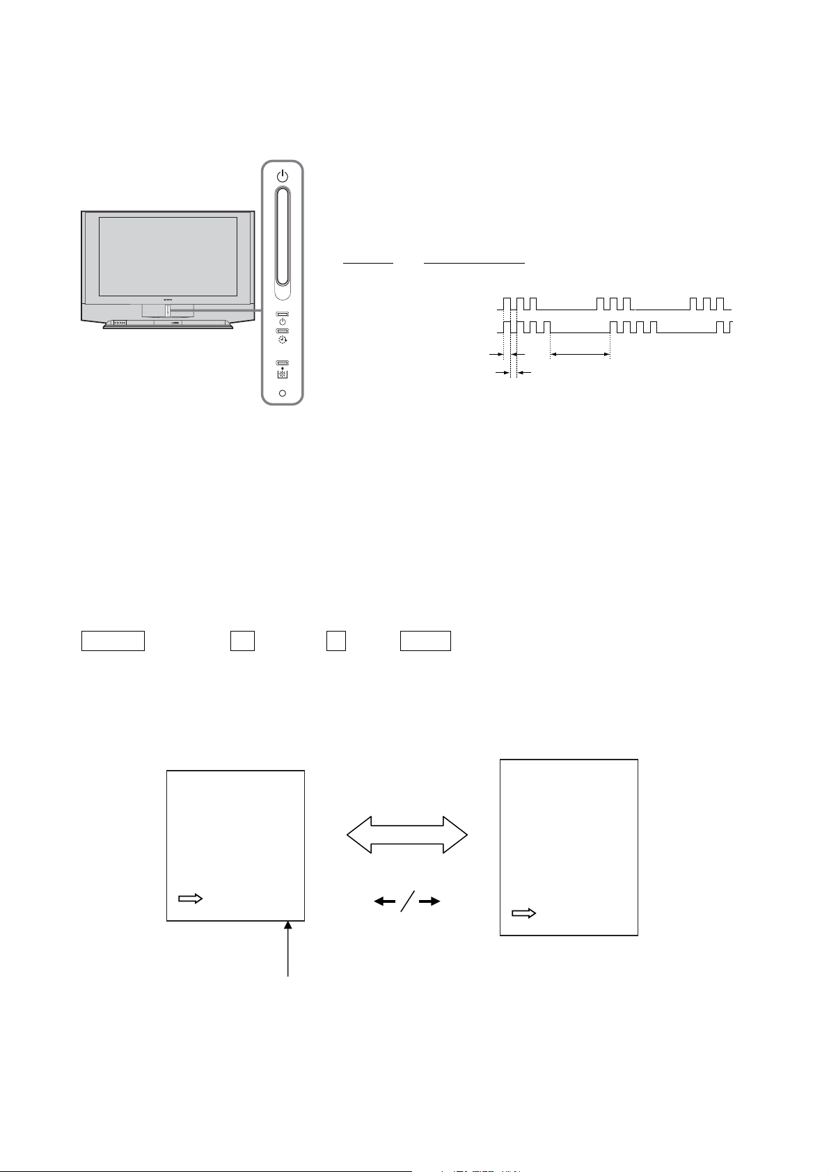
3. Blinking Sequence of POWER/STANDBY LED
• One time blink is not used for self-diagnosis.
• Example
Diagnosis Times of LED blink
• Release of POWER/STANDBY LED blinking
Lamp cover 3 times
Fan 4 times
Lamp ON : 0.3 sec
Lamp OFF : 0.3 sec
The Self-Diagnosis function is released by unplugging the AC
cord temporarily.
Lamp OFF :
3.0 sec
4. Self-diagnosis screen display
• For the failure which is hard to reproduce, or accompany occasional power off and/or picture mute, the Self-diagnosis screen
display is useful to specify the cause.
<To show the screen display>
• Press the keys of the remote commander in rapid sequence as follows, when the set is in standby mode.
DISPLAY t Channel 5 t Vol - t POWER
J
Please note that this differs from
that of entering the service mode (Vol +).
MA
I
N
SELF DIagnosis
MAIN
6:LOWB 0
9:AUDIO 1
101: WDT 0
LCD engine
MENU operation keys
LCD ENGINE
SELF DIagnosis
LCD engine
1:LAMP 0
3:LAMP COVER 0
4:FAN 0
5:LAMP DRIVER 0
201: WDT-ENGINE 0
MAIN
-Numeral "1" means afaultwasdetected one time or more.
-Numeral "0" means that no fault was detected.
– 6 –
Page 7

KF-WE42A1/WE50A1/WS60A1
RM-1022 RM-1022 RM-1022
• The failure record is not automatically cleared.
So after repair, be sure to check the record and set it to “0” manually.
< To clear the failure record >
If the screen display is already on, the following step 1 and 2 can be skipped.
1. Power off (Set to the standby mode)
2. DISPLAY t Channel 5 t Vol - t POWER
3. Channel 8 t ENTER
< To clear the Self-diagnosis screen display >
• The self-diagnosis screen display is cleared by turning off the set with a remote commander or the power switch.
5. Self-Diagnosis function operation
•3 : Lamp cover The rib at the back of the lamp cover closes the SW on T board to ground pin 3 of
CN8001.It’s monitored by the DE-micro (Pin 94 of IC6902) and turns off the lamp when
it’s open.
•4 : Fan Fan rotation is detected by “FAN-PROT”and the DE-micro (Pin 92 of IC6902) turns off the
lamp when it’s “high”.
•4 : Temp When the temperature sensor on the H3 board (WE) or H4 board (WF/XS) detects high
temperature or IIC-E line connector (CN6022:G2 board, CN44: H3/H4 board)is not sested
securely, DE-micro turns off the lamp.
•5 : Lamp driver When the “LAMP-PROT” (pin 95) is low, lamp is not turned on.
If the “LAMP-HV-DET” (pin 96) is low at the same time, it is classified as no high voltage
of the lamp driver.
•6 : Low B error When no “DD 6V” is detected, pin 129 of TV-micro is low and it turns off the main power.
•8 : D-OVP When overvoltage of “+3.3V” or “+2.5V” is detected, pin 126 of TV-micro is low and it
turns off the main power.
•9 : Audio When DC voltage is detected at the speaker or woofer outputs, pin 128 of TV-micro is low
and it turns off the main power.
• LAMP : Lamp When the “LAMP-PROT” (pin 95) is low, lamp is not turned on.
If the “LAMP-HV-DET” (pin 96) is high at the same time, it is classified as no lamp or dead
lamp.
– 7 –
Page 8
KF-WE42A1/WE50A1/WS60A1
RM-1022 RM-1022 RM-1022
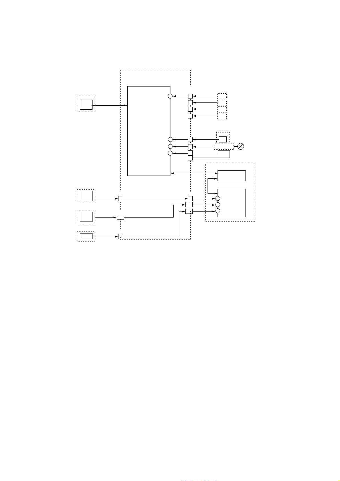
< Self-Diagnosis block diagram>
H3 (WE42A1/WE50A1)/
H4 (WS60A1) board
IC41
Temp
sensor
4:Temp
G2 board
IC6902
Display Engine u-com
IIC-E
CN6000
4:Fan
92FAN PROT
2
FAN1-PRT
5
FAN2-PRT
8
FAN3-PRT
11
FAN4-PRT
Fan1
Fan2
Fan3
Fan4
KD board
Audio
amp
A board
+3.3V
+2.5V
G1 board
DD6V
7:Audio
8:D-OVP
6:LowB
error
CN6029
23
CN6020
C26
CN6029
23
IIC-WE
CN6022
3:Lamp cover
94LAMP-COVER
95LAMP-PROT
96LAMP-HV-DET
14
8
13
14
CN6019
A8
A14
B14
5:Lamp
driver
S8001
SW
Lamp driver
HV-DET
B
IC3801 WE u-com
IIC-WE
IIC-TV
IC3604 TV u-com
IIC-TV
SP_DC_PROT
128
126
D_OVP
129
LB_ERROR
Lamp
T board
– 8 –
Page 9
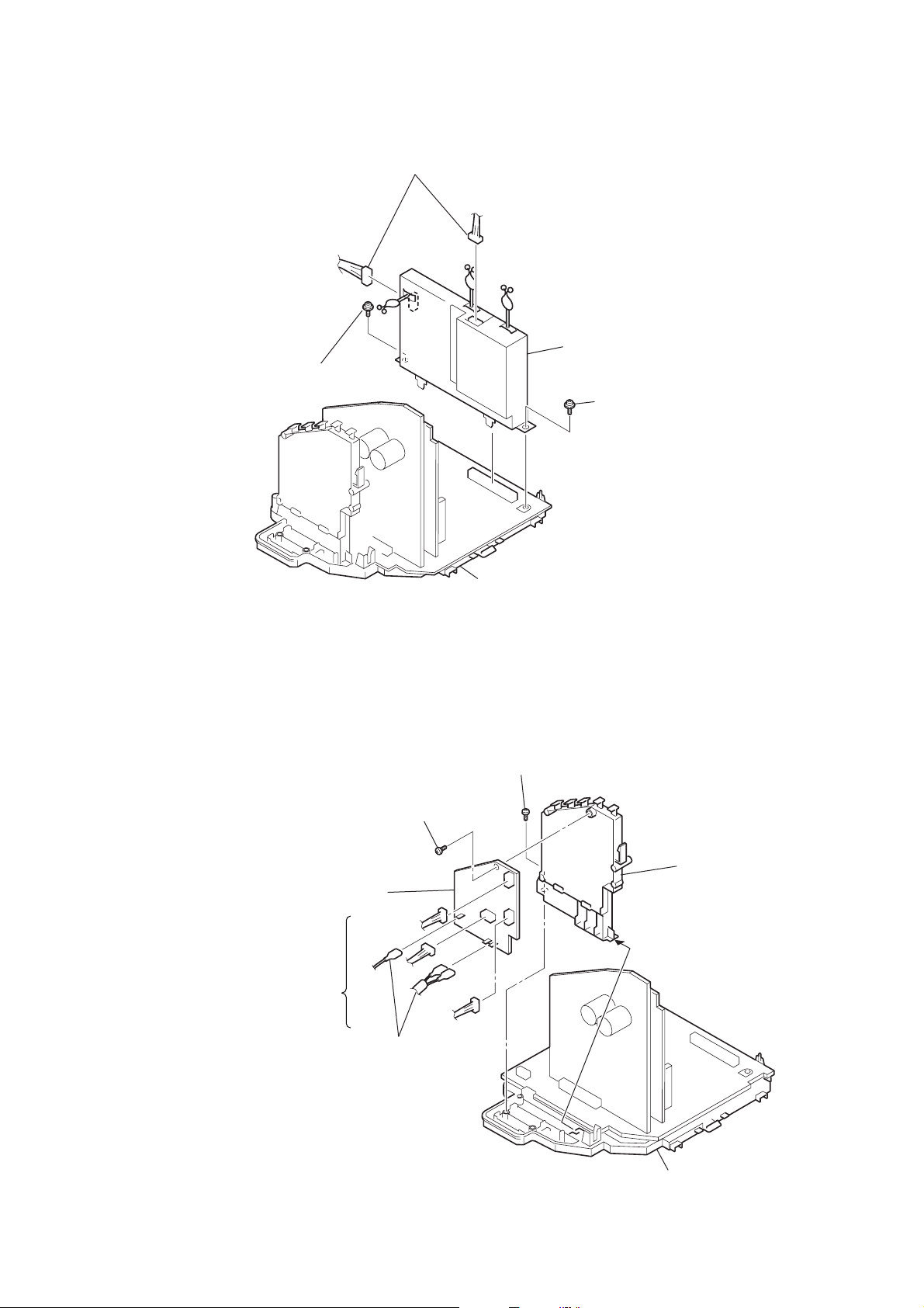
SECTION 2
DISASSEMBLY
KF-WE42A1/WE50A1/WS60A1
RM-1022 RM-1022 RM-1022
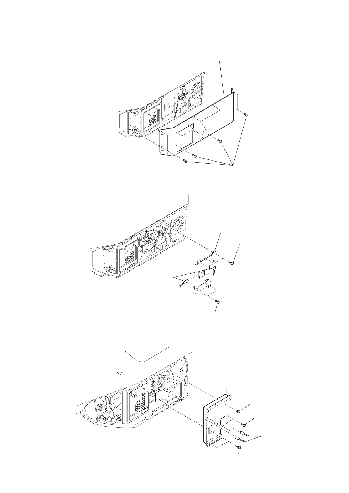
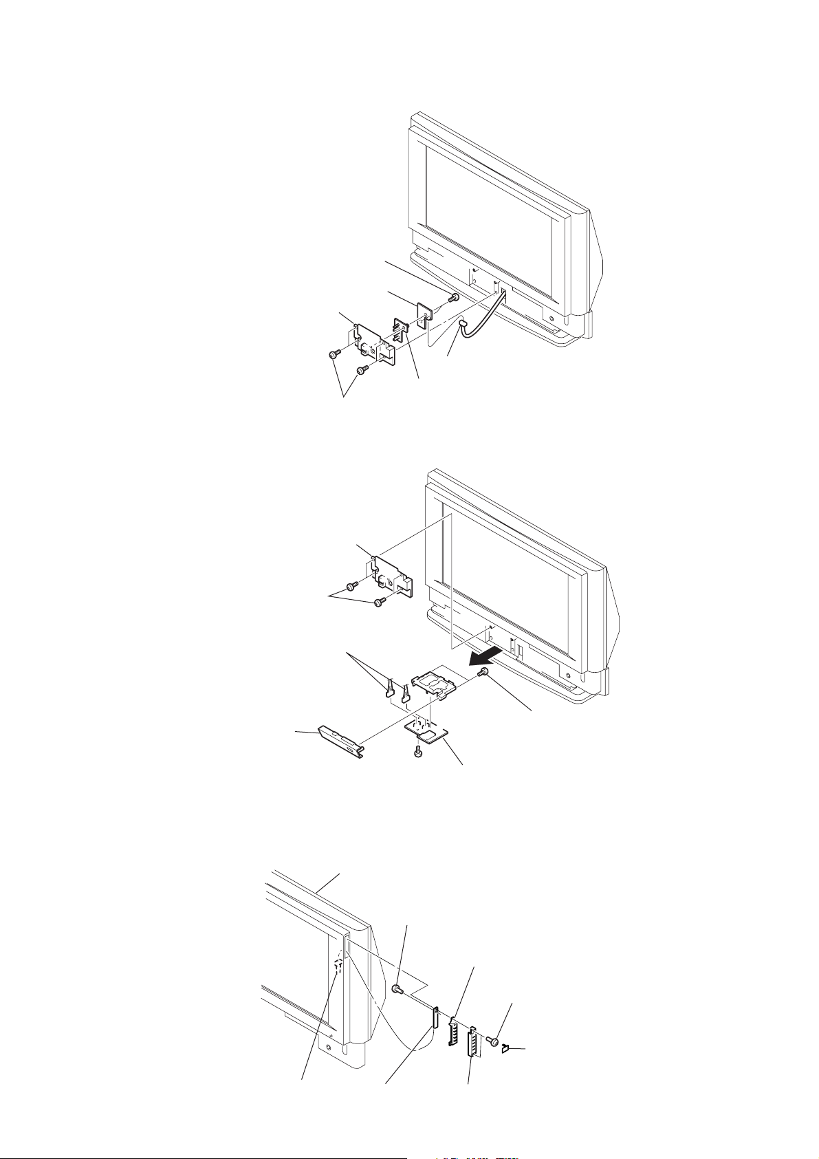
2-1. REAR COVER
2-2. CENTER PILLER ASSEMBLY
(WE42A1/WE50A1)
5 Rear cover
1 Eleven screws
(+BVTP 4x16)
2-3. OU BRACKET (WS60A1)
4 Center pillar assembly
1 Three screws
(+BVTP 4x16)
3 Two
fasten tags
2 Two screws
(+BVTP 4x16)
5 OU bracket
2 Screw
(+BVTP 4x16)
– 9 –
3 Two screws
(+BVTP 4x16)
1 Two
fasten tags
4 Two screws
(+BVTP 4x16)
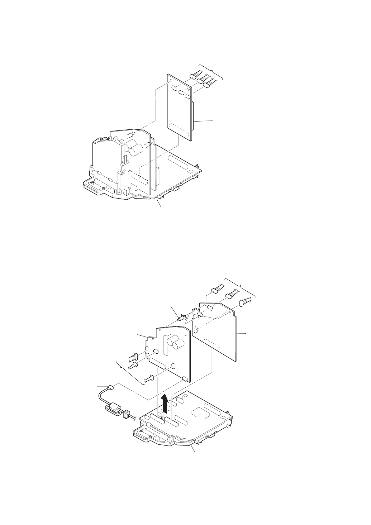
Page 10
KF-WE42A1/WE50A1/WS60A1
RM-1022 RM-1022 RM-1022
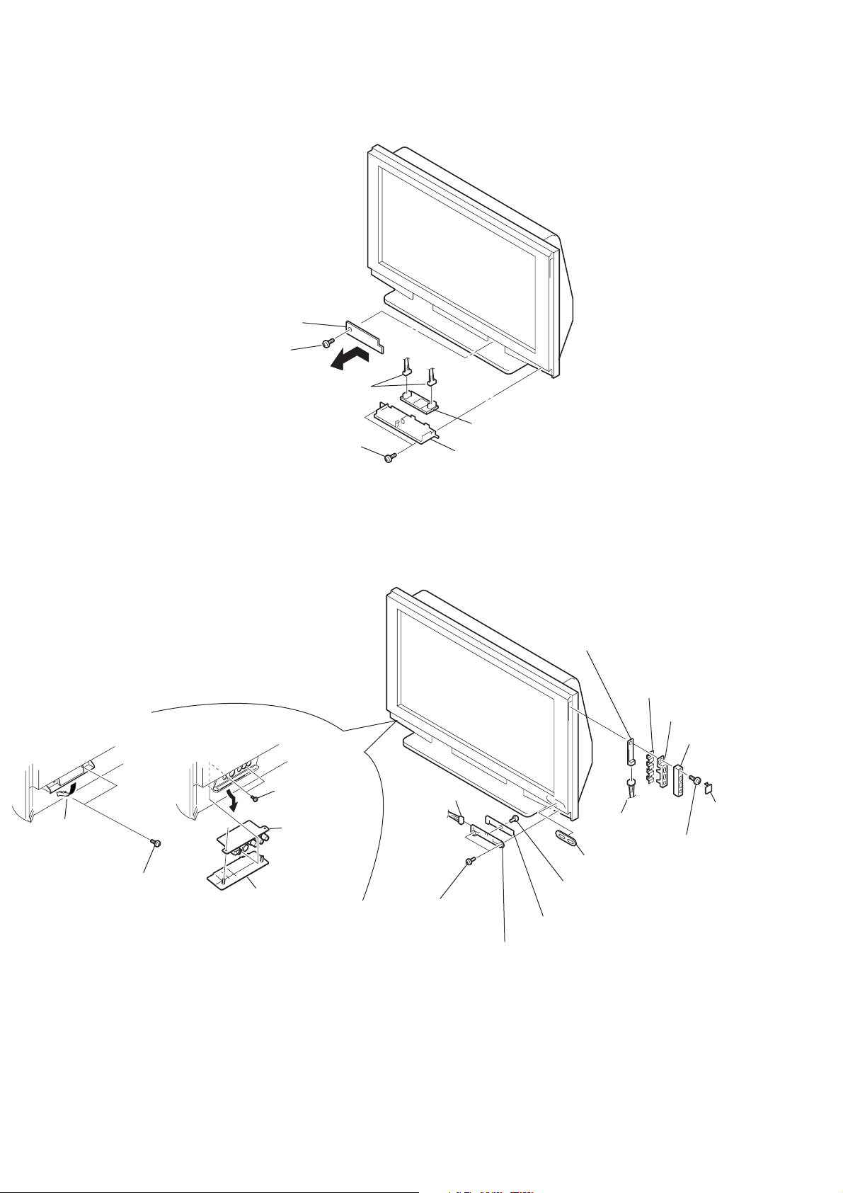
2-4. SERVICE POSITION
Note: In case of the model WE60S1,
first remove the side stay (R).
2-5. CHASSIS ASSEMBLY, OPTICS UNIT (WE42A1/WE50A1)
Chassis assembly
1
8 Two screws
(+PWH 4x35)
7 Connector
9 D. C. FAN
2 Three screws
(+PWH 4x16)
Chassis assembly
4 Three
special screws
1
5
3 Fan bracket
with D. C. fan
6 Optics unit block
2-6. CHASSIS ASSEMBLY, FAN BRACKET (CHASSIS) WITH DC FAN (WS60A1)
4 Chassis assembly
3
2 Side stay (R)
– 10 –
6 Fan bracket (chassis)
with DC fan
1 Screw
(+BVTP 4x16)
5 Three screws
(+PTPWH 4x16)
Page 11
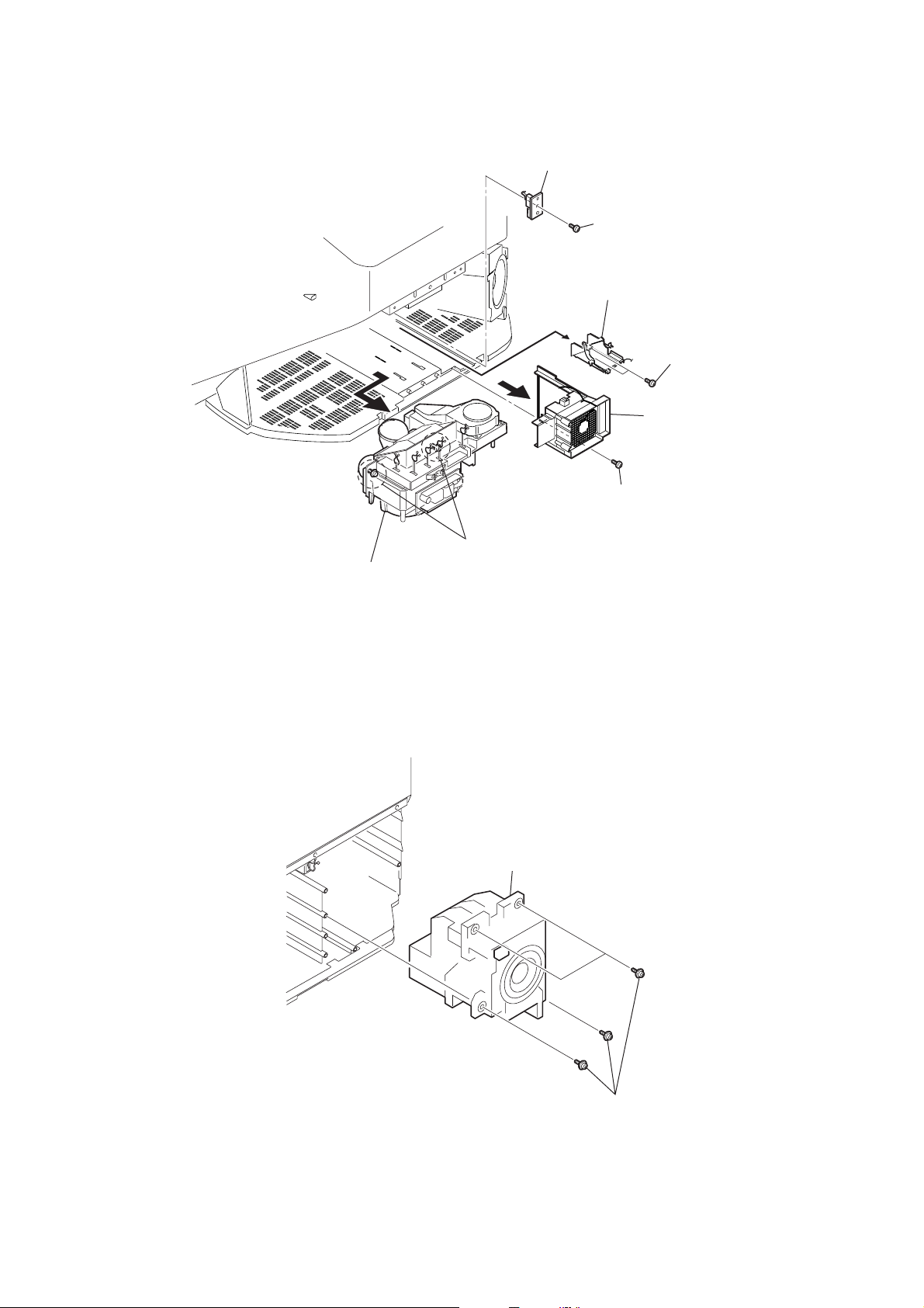
2-7. OPTICS UNIT, FAN DUCT, T BOARD (WS60A1)
5
2
KF-WE42A1/WE50A1/WS60A1
RM-1022 RM-1022 RM-1022
qa T board
0 Screw
(+BVTP 3x12)
9 Duct fan bracket 2
8
7 Two screws
(+BVTP 4x16)
3 Duct fan bracket
with DC fan
4 Loosen two screws
6 Optics unit block assembly
2-8. WOOFER BLOCK ASSEMBLY (WE42A1/WE50A1)
2 Woofer block assembly
1 Screw
(+BVTP 4x16)
– 11 –
1 Four screws
(+PTPWH 4x16)
Page 12
KF-WE42A1/WE50A1/WS60A1
RM-1022 RM-1022 RM-1022
2-9. WOOFER BLOCK ASSEMBLY (WS60A1)
2 Woofer block assembly
1 Four screws
(+PTPWH 4x16)
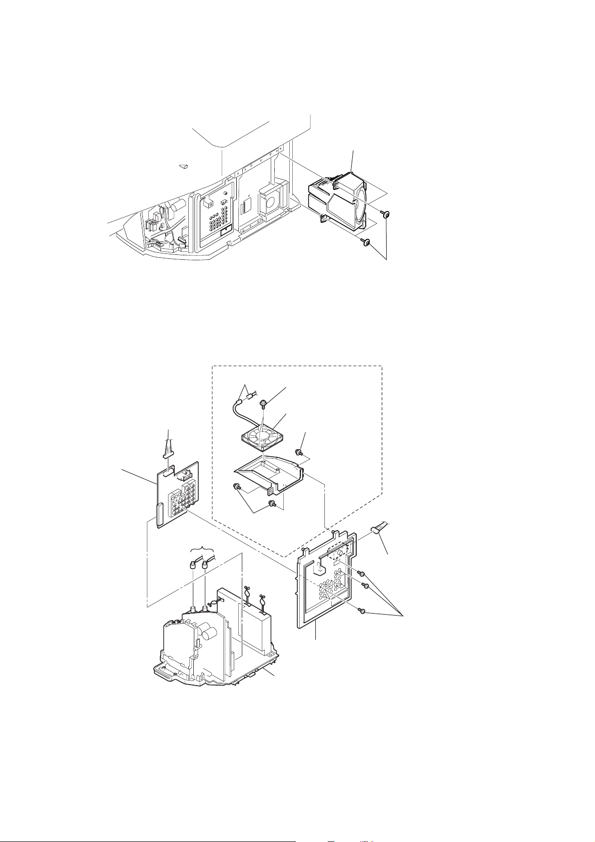
2-10. UG BOARD
0 UG board
8 Connector
9 Connectors
3 Connector
4 Two screws
(+PWH 4x16)
WE42A1/WE50A1
5 Two screws
(+BVTP 4x12)
6 DC fan
4 Screw
(+PWH 4x16)
2 Connector
1 Nine screws
(+BVTP 3x12)
7 UG bracket
Main bracket
– 12 –
Page 13
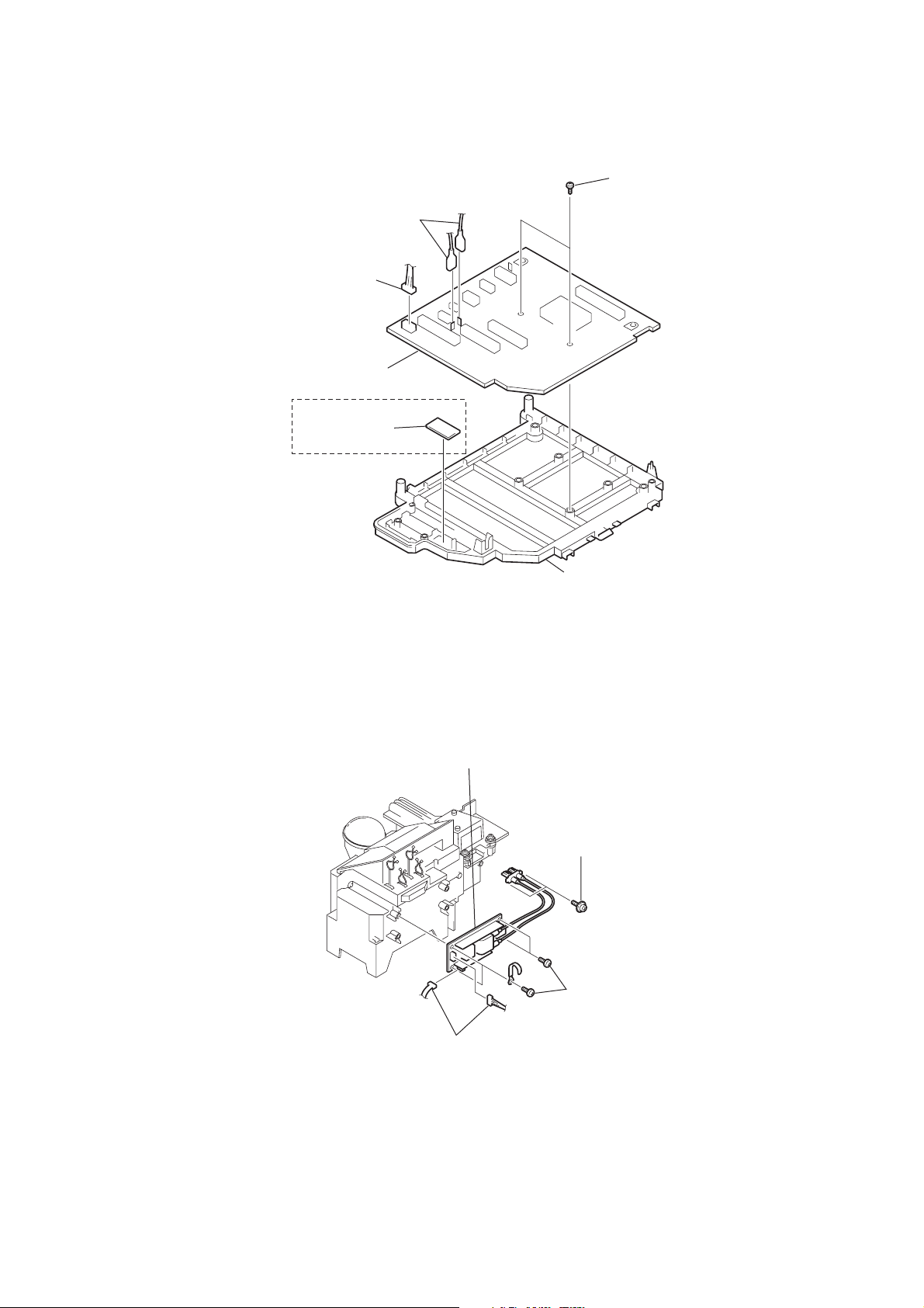
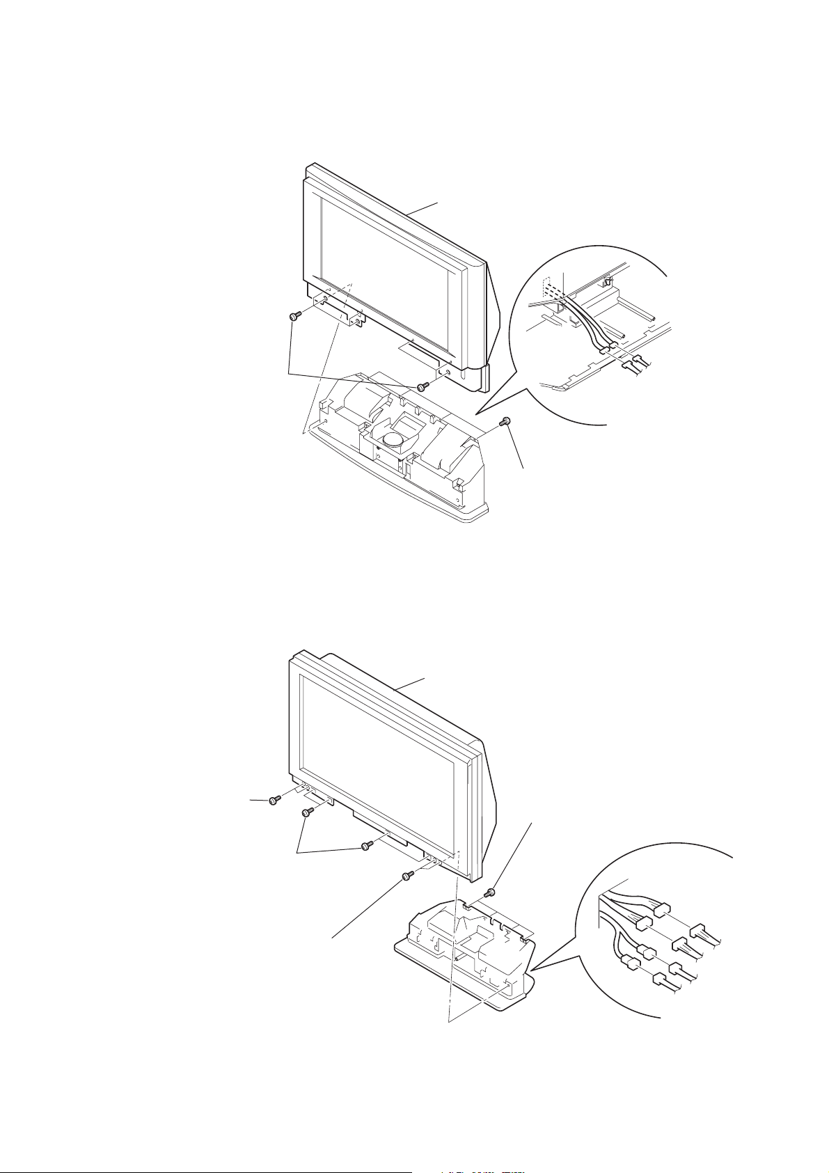
2-11. B BLOCK ASSEMBLY
2 Screw
(+BVWHTP 3x12)
KF-WE42A1/WE50A1/WS60A1
RM-1022 RM-1022 RM-1022
1 Two connectors
3 B block assembly
2 Screw
(+BVWHTP 3x12)
2-12. F BOARD
2 Three connectors
3 Screw
(+BVTP 3x12)
4 F board
1 Three fasten tags
Main bracket
3 Screw
(+BVTP 3x12)
4 F bracket
with F board
– 13 –
Main bracket
Page 14
KF-WE42A1/WE50A1/WS60A1
RM-1022 RM-1022 RM-1022
2-13. KD BOARD
1 Three connectors
2 KD board
2-14. AG AND G1 BOARDS
2 Three
connectors
1 Power cord
6 G1 board
Main bracet
3 Three connectors
5 Three
board suppoters
7 AG board
4
– 14 –
Main bracet
Page 15
2-15. G2 AND H4 (WS60A1) BOARDS
1 Two
fasten tags
3 Connector
4 G2 board
5 H4 board
WS60A1
KF-WE42A1/WE50A1/WS60A1
RM-1022 RM-1022 RM-1022
2 Two screws
(+BVTP 3x12)
2-16. POWER SUPPLY BLOCK
4 Power supply block
Main br
acket
2 Two screws
(+PWH 3x10)
3 Four screws
(+BVTP 3x12)
1 Two connectors
– 15 –
Page 16
KF-WE42A1/WE50A1/WS60A1
RM-1022 RM-1022 RM-1022
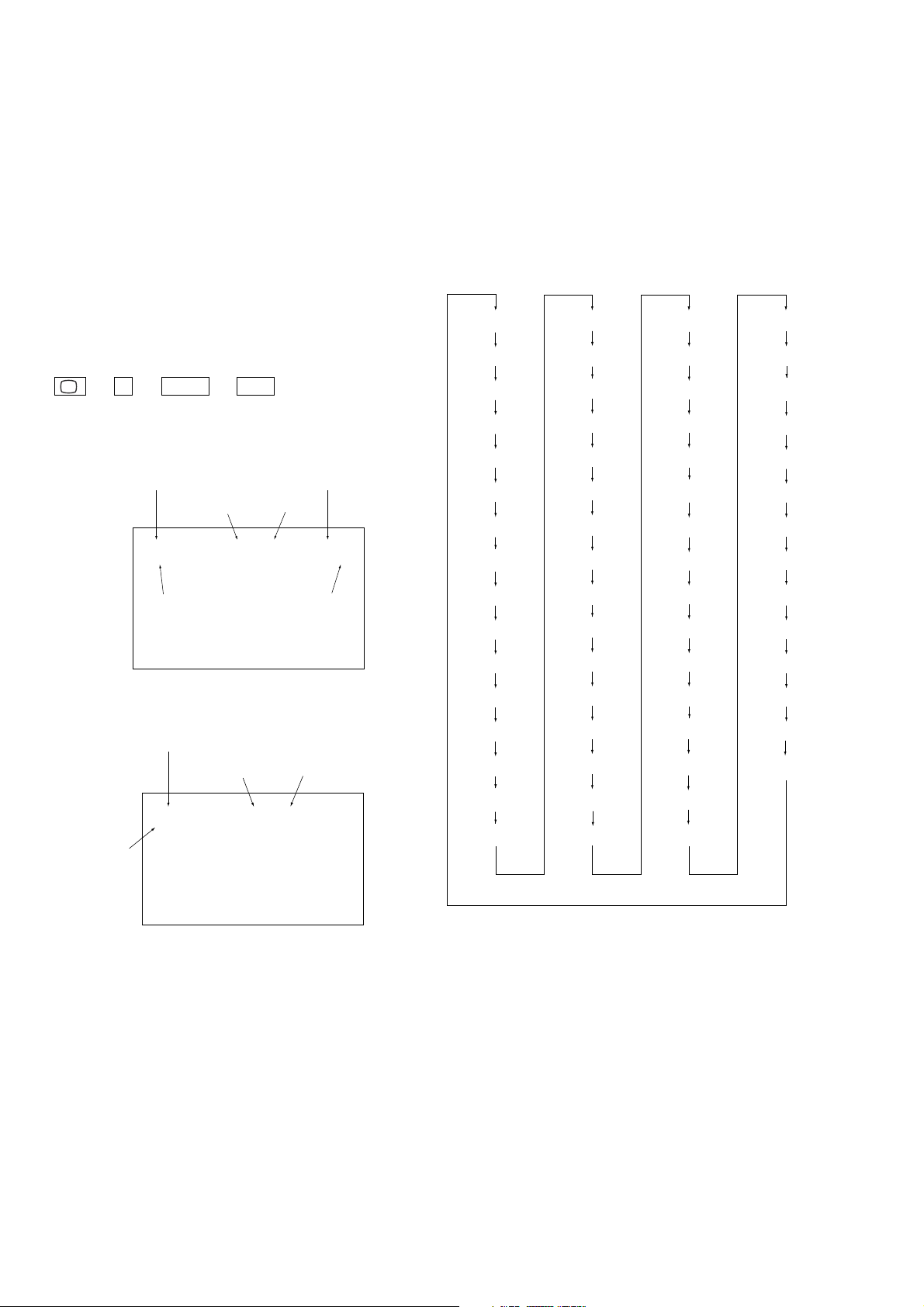
2-17. T BOARD (WE42A1/WE50A1)
3 T board
2 Screw
(+BVTP 3x12)
1 Connector
2-18. H3 BOARD (WE42A1)
6 H3 board
2 Fasten tag
1 Three
connectors
1
4 H3 bracket
3 Two screws
(+BVTP 3x12)
2-20. HMG AND H3 BOARDS (WE50A1)
8 Fasten tag
5 Spring
plate
2-19. FRONT COVER ASSEMBLY (WE42A1/WE50A1)
1 Two ornamental screws
Front cover assembly
2
Four latches
qd H3 board
qs Spring
plate
qa H3 bracket
5 Two Connectors
9 Three
connectors
0 Two screws
(+BVTP 3x12)
3 Two screws
(+BVTP 4x16)
4 MS bracket
1 Five screws
(+BVTP 4x16)
7 HMG board
6 Screw
(+BVTP 4x16)
2 Bottom cover assembly
– 16 –
Page 17
2-21. H2 BOARD (WE42A1/WE50A1)
4 Two screws
(+BVTP 3x12)
2 H2 bracket
1 Four screws
(+BVTP 4x16)
KF-WE42A1/WE50A1/WS60A1
RM-1022 RM-1022 RM-1022
5 H2 board
3 Connector
6 Light guide (LED)
2-22. HMG BOARD (WE42A1)
2 H2 block assembly
1 Four screws
(+BVTP 4x16)
5 Two Connectors
7 MS panel
2-23. H1 BOARD (WE42A1/WE50A1)
3
4 Two screws
(+BVTP 4x16)
6 HMG board
3 Connector
Screen mirror block assembly
4 Screw
(+BVTP 3x12)
6 H1 button
5 H1 board
H1 bracket
– 17 –
2 Two screws
(+BVTP 4x16)
1 H1 bracket cap
Page 18
KF-WE42A1/WE50A1/WS60A1
RM-1022 RM-1022 RM-1022
2-24. HMG BOARD (WS60A1)
3 Cover (60), Cable
1 Screw
(+BVTP 3x12)
6 Two connectors
2
4 Two screws
(+BVTP 3x12)
2-25. H1, H2 AND H3 BOARDS (WS60A1)
A
3 Two screws
(+BVTP 3x12)
1 Open
H3 block
A
2 Two screws
(+BVTP 3x12)
5 H3 board
4 H3 bracket (R)
5 HM bracket
with HMG board
9 Connector
7 Two screws
(+BVTP 3x12)
7 HMG board
qa H2 board
qk H1 board
qf Connector
6 MS panel
0 Screw
(+BVTP 3x12)
qj Insulating sheet
(H1)
qh H1 button
qg H1 bracket
qs H1 bracket
cap
qd Screw
(+BVTP 3x12)
– 18 –
8
H2 bracket
Page 19
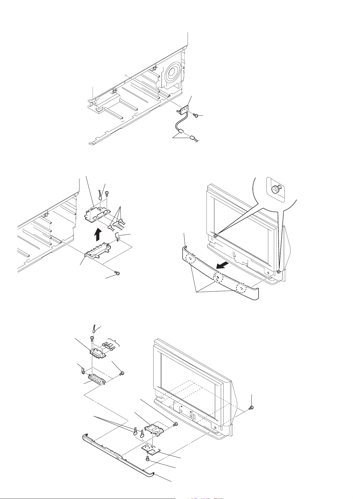
2-26. SCREEN MIRROR BLOCK ASSEMBLY
(WE42A1/WE50A1)
3 Seven screws
(+BVTP 4x16)
KF-WE42A1/WE50A1/WS60A1
RM-1022 RM-1022 RM-1022
4 Screen mirror block assembly
1 Two
connectors
2-27. SCREEN MIRROR BLOCK ASSEMBLY
(WS60A1)
4 Two screws
(+BVTP 4x20)
2 Four screws
(+BVTP 4x16)
2 Four screws
(+BVTP 4x16)
5 Screen mirror block assembly
3 Four screws
(+BVTP 4x16)
1 Four
connectors
4 Two screws
(+BVTP 4x20)
– 19 –
Page 20
KF-WE42A1/WE50A1/WS60A1
RM-1022 RM-1022 RM-1022
SECTION 3
ELECTRICAL ADJUSTMENTS
3-1. ELECTRICAL ADJUSTMENT BY REMOTE
COMMANDER
By using remote commander (RM-1022), all circuit adjustments
can be made.
NOTE : Test Equipment Required.
1. Pattern Generator (with component outputs)
2. Oscilloscope
3. Digital multimeter
3-1-2. Service Mode Adjustment
1. The SCREEN displays the item being adjusted.
2. Press “1” or “4” on the remote commander to select the
adjustment item.
3. Press “3” or “6” on the remote commander to change the data.
4. Press “2” or “5” on the remote commander to select the category.
Every time you press “2” (Category up), Service mode changes in
the order as shown below.
3-1-1. Method of Setting the Service Adjustment
Mode
1. Standby mode. (Power off)
2. t 5 t 2 (+) t ^/1
on the remote commander.
(Press each button within a second.)
The following service screen will appear.
Category Name
Item No.
3D-COMB 0 0 SERVICE
NRMD TV
Item Name Input Signal
F/A FLAG: xxxxxxxx
CBA FLAG: xxxxxxxx
Category Name
WSL: xxx
Item No.
Mode
Data
Data
(TV)
VERSION
CXA2209Q
AP
DLBY
BUSSW
CXA2103
CXA2163
2DCOMB
TELETEXT
MSPSIZE
MSPMD
MSPSEL
MSPFNC
MSP3714G
OSD
CC M
CC S
CC T
OPB GA
OP GA
OP US
(WEM2)
CCP-INT
CCP-OSD
CCP-BLK
CCP-ADJ1
CCP-ADJ2
CCP-USER
SNNR
DRCVR
USER-NR
LPFC
ID
CCP-1-12
OVSN
(
PANEL
A7001R
A7001G
A7001B
GB-RGB
FAN-CNT1
FAN-CNT2
OP
)
OP
OPTION_E
S_MAS_M
S_MAS_S
J_L004
D9809_1
D9809PIC
D9809TPN
D9809CUR
D9809TG1
D9809OSD
D9809HPF
D9809OSC
D9809CGA
D9809HUE
Item Name
L001OUT 0 0 G
OCKPN
TEMP 42DEG
LCD PJ ENGINE VER.0.026
<LCD PROJECTOR ENGINE>
9/11
EE2F
CCPS 1-11
DELAY 1-2
CCP-AVP
MID-1-9
TEMP
OSD_E
5. If you want to recover the latest values press “-” then
“[ENTER]” to read the memory.
6. Press “[MUTING]” then “[ENTER]” to write into memory.
7. Turn power off.
Note: Press “8” then “[ENTER]” on the remote commander
to set the shipping conditions or turn set off and on to
exit.
3-1-3. Memory Write Confirmation Method
1. After adjustment, turn power off with the remote com-
mander.
2. Turn power on and set to service mode.
3. Call the adjusted items again and confirm they were adjusted.
– 20 –
Page 21
KF-WE42A1/WE50A1/WS60A1
RM-1022 RM-1022 RM-1022
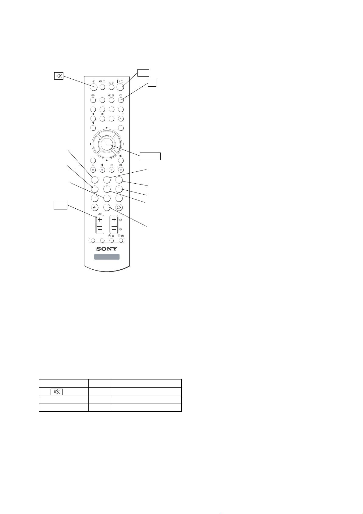
3-1-4. Adjusting Buttons and Indicator
VIDEO
HD/DVD
CENTER
WEGA
SP
THEATRE
V CENTER
A/B
MENU
R
O
P
G
N
I
+
W
-
W
G
I
O
N
R
P
Adjustment item
up
Adjustment item
DRC-MF
PROG
INDEX
FREEZE
T
T
down
1
2
User control goes
to the standerd state
(Shipping Conditions)
2 +
4
7
OPTION RESET
3
5
6
8
9
0
PROG
TV
RM-1022
FUNCTION OF KEYS ON COMMANDER
• 1 : Changes adjustment item. (item No. moves up)
• 4 : Changes adjustment item. (item No. moves down)
• 2 : Changes adjustment category.
(category moves up)
• 5 : Changes adjustment category.
(category moves down)
• 3 : Changes data value. (up)
• 6 : Changes data value. (down)
Commander Function
Button Mode Description
+ [ENTER] WRITE Writes data to NVM.
- + [ENTER] READ Reads data from NVM.
8 + [ENTER] RESET Set the shipping condition.
(Be sure not to use usually)
^/1
a
ENTER
Adjustment category
up
Data up
Data down
Adjustment category
down
Read data from
NVM
3-1-5. 3D gamma internal signals
3D gamma IC has the following 11 internal signal patterns .
With service menu “D9809TPN 4 TPNMODE “ setting ,
0 Plain ( white )
1 Stripe
2 Checker ( small )
3 Lattice
4 Cross-hutch
5 Cross-point
6 Ramp
7 Stair steps
8 Checker ( large )
9 Diagonal
10 Window
Internal signal control service menu
D9809TPN 0 TPNSW Test Pattern ON = 1, OFF = 0
1 TPNRGB Test Pattern color select
2 SBTPNSW Sub Test Pattern ON = 1, OFF = 0
3 SBTPNRGB Sub Test Pattern color select
4 TPNMODE Test Pattern select
5 TPNHV H/V select H = 0 , V = 1
6 TPNINV Level invert invert = 1
7 TPNREP Pattern repeat enable
(only for 6 and 7)
8 STRSTEP Stair steps select 9 = 0 , 17 = 1
(only for 7)
9 U/DMODE Up/Down enable
(only for 6 and 7)
10 TPSLANT Bottom level select
(only for 6 and 7)
11 TPPRMTR Pattern width (except 0 and 9)
12 TPNPOSH H position
(only for 4,5,6,7 and 10)
13 TPNPOSV V position
(only for 4,5,6,7 and 10)
14 RLVL-H R Upper Level (except 6 and 7)
15 RLVL-L R Lower Level (except 6 and 7)
16 GLVL-H G Upper Level (except 6 and 7)
17 GLVL-L G Lower Level (except 6 and 7)
18 BLVL-H B Upper Level (except 6 and 7)
19 BLVL-L B Lower Level (except 6 and 7)
3-1-6. Service List
For details, please reter to the appendix at the end of this manual.
– 21 –
Page 22
KF-WE42A1/WE50A1/WS60A1
RM-1022 RM-1022 RM-1022
3-2. To read Lamp and Panel time
The lamp and panel time of the set are displayed as follows .
<Enter the service mode>
1. Press the keys of the remote commander in rapid sequence as fol-
lows , when the set is in standby mode.
DISPLAY t Channel 5 t Vol + t POWER
2. Press the “JUMP ” key [3 times].
You’ll get into DE-micro service menu .
3. Press “2 ” key [9 times] to show the following display .
Example
PANEL NVM OK 9 OPTION_E
0 LAMP 0 Diff 1
LampTM 14 LampCT 71
This screen reads
“Total lamp time is 14 hours” and
“Total lamp ON/OFF cycle is 71 times”
To reset lamp time,
press “3 ” , “MUTE ” and “ENTER ” keys in sequence.
WRI-EXE(Red Character) is momentarily displayed and LampTM
will be reset to “0 ”.
4. Press “ 1 ” key [7 times].
Example
PANEL NVM OK 9 OPTION_E
7 SH SFT1 10 Diff 1
PanelTM 14h
Please record the steps shifted as MDHP and MDVP .
MID-X1 9 MDHP (for H center)
10 MDVP (for V center)
MDVP
MDHP
3, Change the WIDE mode to “Normal “ and change the register
data as follows .
MID-X1 9 MDHP + MDHP
(Don't change MDVP data)
4, Display the Twin Picture with the “split “button of the remote
commander and change the registers data as follows .
MID-X1 9 MDHP + MDHP
10 MDVP + MDVP
This screen reads
“Total Panel time is 14 hours”
You can’t reset the Panel time with the Service menu .
<To get out of the Service menu>
The Service menu is cleared by turning off the set with a remote com-
mander or the power switch .
3-3. Test Reset
The user settings can be reset to the factory default condition as fol-
lows.
1. Press “TEST “ and “RESET “ key in sequence when the set is ON .
The LAMP,TIMER and POWER/STANDBY LED light and the
picture is muted.
After about 5 seconds the LAMP and TIMER LED go off,
and the color of POWER/STANDBY LED changes from amber
to green.
After another 10 seconds the reset is completed and the initial set-
up display appears.
3-4. LA-3 H/V Center Confirmation and Adjust-
ment
Please check the picture horizontal/vertical center after the replace-
ment of the following parts .
• Optical block
• Top assembly
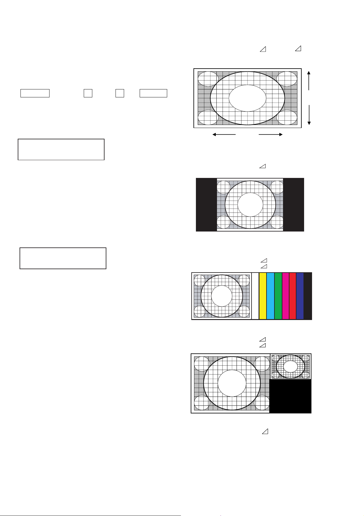
1, Check H/V center with 480i monoscope signal in “Full “ mode .
2, If the center is shifted , adjust it with the following service items .
5, Press “Favorites” button and change the registers data as follows .
MID-X1 9 MDHP + MDHP
10 MDVP + MDVP
6, OSD horizontal position must be adjusted as follows .
DCP-OSD 17 RP1L +
MDHPx2
If above sum exceeds 255, set 1 to “16 RP1H ” and set the “sum-256”
to “17 RP1L”
Please be careful since the registers are different from other cases .
And don’t forget to write the data before changing the display/wide
mode .
– 22 –
Page 23
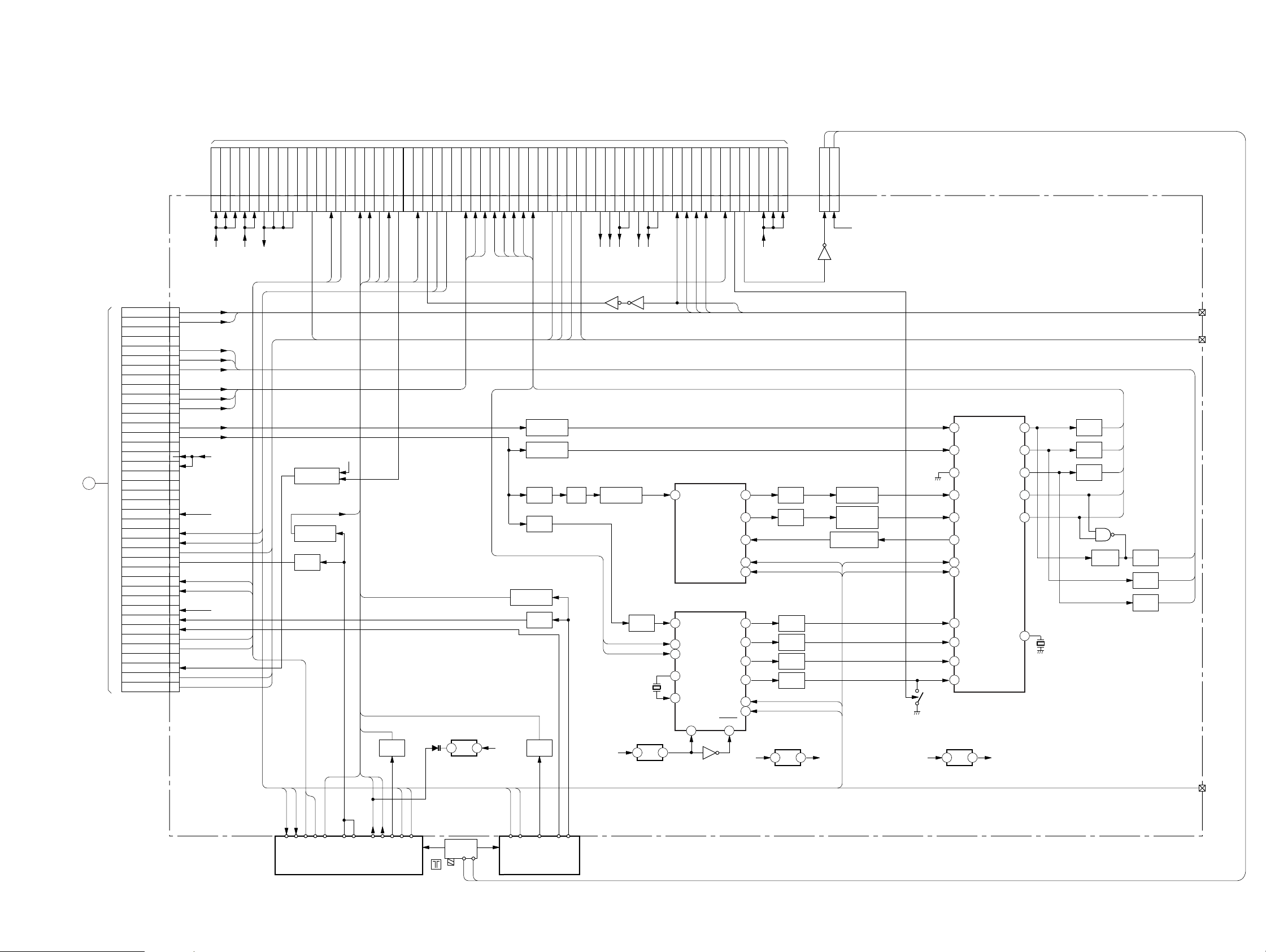
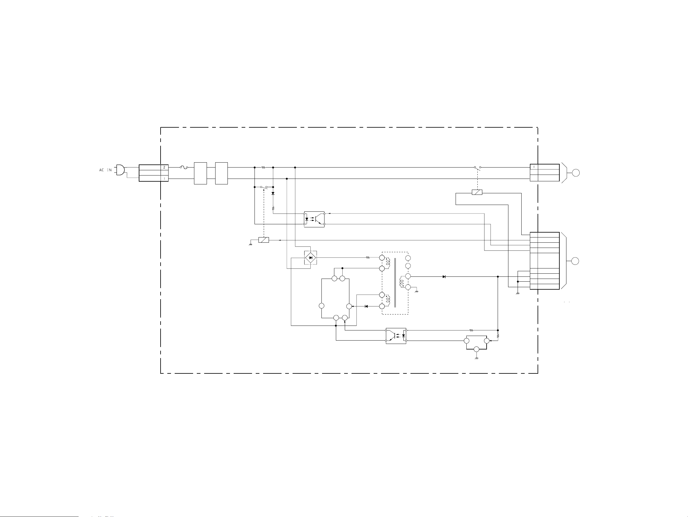
4-1. BLOCK DIAGRAM (1)
SECTION 4
DIAGRAMS
TO
G2 BOARD
CN6020
KF-WE42A1/WE50A1/WS60A1
RM-1022 RM-1022 RM-1022
A
TO
UG BOARD
CN1501
CN8001
MAIN-R
MAIN-L
VAR/FIX-R
VAR/FIX-L
TEXT-PR
TEXT-PB
TEXT-Y
MAIN-PR
MAIN-C/PB
MAIN-Y
SUB-C
SUB-Y/CV
INS-C
INS-Y/CV
SCLK-TV
SDAT-TV
SIRCS
MT-CV
MT-R
MT-L
STBY 5V
ST-CV
ST-L
MS-R
MS-L
MAUMUTE
HDMI-RST
HDMI(AU)SW
CN8004
3.3V
3.3V
2.5V
2.5V
3.3V
+
+
+
+
+
C32
B32
C30
B30
C28 DD 6V
B28 DD 6V
C27 DD 6V
B27 DD 6V
DD 6V
50
49
47
46
44
43
40
37
36
33
MAIN-R
MAIN-L
NC
NC
TEXT-PR
TEXT-PB
MAIN-PR
MAIN-PB
MAIN-Y
TEXT-Y
3.3V
+
A32
2.5V
+
30
29
NC
NC
SCL
SDA
SIRCS
MT-R
MT-L
+
5V
+
9V
STBY 5V
Q8015-8017
MUTE SWITCH
SYNC DETECT
Q8002
BUFFER
28
5V
27
5V
25
24
22
9V
20
19
18
15
12
11
9
8
7
MS-R
5
MS-L
4
3
HDMI-RST
2
YUV-SW
1
C26 DD OVP
DD OVP
M-HSYNC
Q8005
3.3V
+
C25
MS-R
3.3V
+
A25
MS-L
+
9V
C23 SUB-HS
B23 MAIN-HS
S-HSYNC
M-HMSYNC
S-HSYNC
C22 MAIN-AFT
B22 SUB-AFT
SAFT
MAFT
C21 F-MONO
A22 AGC-ATT
I-SAP
B21 I-SAP
A21 O-SAP
C20 SDAT-TV
SCL
SDA
B20 SCL-TV
C19 MAIN-PR
B19 MAIN-PB
MAIN-PB
MAIN-PR
A19 MAIN-Y
PR
MAIN-Y
C18 SUB-PR
B18 SUB-PB
Y
PB
HD, VD
SYNC DETECT
C17 SUB-H
A18 SUB-Y
HD
Q8006
B17 SUB-V
VD
YUV-SW
Q8224,8223
BUFFER
Q8226,8225
BUFFER
Q8215
BUFFER
Q8227
BUFFER
Q8004
BUFFER
C16 HDMI-RST
A17 YUV-SW
SIRCS
HDMI-RST
FL8201
LPF
B16 SIRCS
A16 VAR-MUTE
VAR-MUTE
33V
9V
+
+
C14 STBY 5V
C12
C11
9V+5V
33V
+
+
STBY 5V
Q8013 Q8014
Q8213,8211
BUFFER
HD
VD
SAFT
MAFT
Q8011
BUFFER
IC8001
RESET
1 2
+
Q8012
5V
BUFFER
+3.3V
9V
11V
+
+
B11
C10
11V
+
Q8606
BUFFER
X8601
12MHz
IC8603
RESET
5 4
5V
5V
+
+
C8
C9
A7 HP-SW
A6 AU-W
R
WF
IC8201
COMB FILTER Y/C SEPALATOR
7 YC IN 25
IC8601
TELETEXT DECODER
31 CVBS0
53 HSYNC
55 VSYNC
71 XTALOUT
70
XTALIN
RESET RESET
73 72
C5 RCH
L
HP-SW
Q8601
A5 LCH
A4 APC-SW
C3 TEXT-BLK
B3 O-ATT
APC-SW
Y OUT
C OUT
27
19
SDA
16
SCL
15
R
48
G
47
46
B
52
SDA0
82
SLL0
81
+5V +3.3V
1.8V
1.8V
+
+
C1
B1
1.8V
+
Q8206
BUFFER
Q8201
BUFFER
BUFFER
BUFFER
BUFFER
BUFFER
IC8602
3.3V REG.
5 4
1.8V
+
A1
Q8604
Q8605
Q8607
Q8609
CN8003
2 ATT-SW
SDA
SCL
SDA
SCL
19V
+
9V
Q8010
Q8207-8209
CLAMP
Q8202,8203
Q8205
CLAMP
Q8218,8220
WAVE SHAPER
SDA
SCL
TEXT_R
TEXT_G
TEXT_B
BLK
IC8202
SUB COLOR DECODER
43 C2
44 CVBS/Y2
86 YS2/YM
1CVBS/Y1
48 C1
46
FSC OUT
14 SDA
13 SCL
35
R2
34
G2
33
B2
36VDS
YS2/YM
Q8204
IC8207
+5V REG.
+9V +5V
I O
Y OUT
Cb OUT
Cr OUT
Xtal
AUDIO
)
AG(2/2
CTR
)
AG(2/2
Y
X8201
Q8214
BUFFER
Q8212
BUFFER
Q8210
BUFFER
1
2
Q8222
BUFFER
CB
CR
HD
VD
IC8203
4
Q8221
BUFFER
Q8219
BUFFER
Q8216
BUFFER
TEXT_Y
TEXT_CB
TEXT_CR
21
22
23
HS
9
VS
4
38
SDA
SCL
MUTE
MT-L
MT-R
NC
L OUT
– 23 –
R OUT
MUTE
DET OUT
DET OUT2
I-SAP
BIL LED
APC-SW
ST LED
SDA
SDA
AFT OUT
SCL
SCL
RF
SPLITTER
SCL
SCL
SDA
SDA
AFT OUT
DET OUT
DE-EM OUT
AG (1/2) (TUNER/COLOR DECODER)
– 24 –
I2C
AG(2/2
)
Page 24
KF-WE42A1/WE50A1/WS60A1
RM-1022 RM-1022 RM-1022
BLOCK DIAGRAM (2)
AUDIO
)
AG(2/2
CTR
)
AG(2/2
MAIN-L
MAIN-R
VAR-MUTE
IC8404
AUDIO PROCESSOR
64 L IN
R IN
63
SDA
22
23
SCL
+
9V
OUT A
OUT B
LF IN B
LF OUT B
Q8402,8403
Q8405
MUTE SWITCH
AG (2/2)
(AUDIO PROCESSOR/REGULATOR)
11V
L-MUTE
Q8401
BIAS
Q8406
Q8411
Q8416
BUFFER
IC8403
HEADPHONE AMP
351
7
IC8402
FILTER-W
351
IC8405
3 1
Q8412,8413
MUTE
LPF
L
Q8404
BUFFER
R
Q8409
7
BUFFER
WF
CN8002
4
HP-SW
3
HP-L
1
HP-R
WE42 / WE50
TO
H3 BOARD
B
CN4302
WS60
TO
H3 BOARD
C
CN6302
+
16
36
35
34
I2C
AG(2/2
HP-SW
IC8205
DD6V
+2.5V
DD OVP
)
Q8232
+3.3V
D8206
D8210
Q8205
SWITCHING
DRIVER
DD6V
Q8223
SWITCHING
DRIVER
+2.5V/+3.3V
SWITCHING REGULATOR
29 OUT1
U
L
OUT1
64
INV1
1
64 OUT2
U
64 OUT2
L
15
INV2
IC8204
+1.8V
SWITCHING REGULATOR
4
VCC
DD6V
24
DD6V
1+1.8V 2
1HM3.3V
2HM3.3V
CN8202
WE42 / WE50 WS60
TO
HMG BOARD
CN2306
D
E
Q8230.8231
+B OFF DETECT
IC8206
+3.3V
SWITCHING REGULATOR
4
TO
HMG BOARD
CN5306
D8202
12
D8211
1SET 11V
2SET 11V
5MS 3.3V OVP
6MS 3.3V-DET
9MS 3.3V
10MS 3.3V
CN8201
TO
G1 BOARD
CN6001
– 25 –
– 26 –
Page 25
BLOCK DIAGRAM (3)
KF-WE42A1/WE50A1/WS60A1
RM-1022 RM-1022 RM-1022
CN1900
AC (L)
AC (N)
F1901
T1900
LINE
FILTER
T1901
LINE
FILTER
RY1900
D1161
PH1901
D1900
RECTFIER
SWITCHING
REGULATOR
1
8
Q1900
3 4
CN1909
AC (L)
4
AC (N)
RY1901
CN1908
8
AC ON
7
T1902
SBT
4
3
7
1
2
D1909
2
ISOLATOR
11
10
9
D1912
8
PH1902
6
5
4
3
2
1
DTL 5V
PROT
DTL 9V
GND
STBY 5V
GND
AC-RLY (–)
G1 BOARD
F
CN1604
G1 BOARD
G
CN1601
TO
TO
F (LINE FILTER)
– 27 –
IC1602
SHUNT
REGULATOR
3 1RK
A
2
– 28 –
Page 26
KF-WE42A1/WE50A1/WS60A1
RM-1022 RM-1022 RM-1022
BLOCK DIAGRAM (4)
WE42/WE50
CHOKE
COIL
TO F BOARD
CN1909
CN1602
LAMP GND
3
1
C28
C27
C26
C25
C24
C23
C22
C21
C20
C19
C18
C17
C16
C15
C14
C13
C12
C11
C9
C8
C7
C6
C5NC
C3
C2
LAMP DC
CN1605
SET 17V
SET 17V
SET 5V
SET 5V
SET 5V
SET 11V
SET 11V
SET 11V
SET 11V
DD 6V
DD 6V
DD 6V
DD 6V
SET 6V
SET 6V
SET 9V
SET 9V
SET 9V
TU 33V
STBY 5V
AC-RLY (–)
AC-RLY (+)
MAIN-CTL
POW-CTLC4
LOWB-DET
MS3.3V OVP
D1631
D1634
D1640
IC1607
SHUNT
REGULATOR
KR
3
A
2
D1645
R1754
D1635
D1641
D1629
D1633
D1630
1
Q1620,D1647
+33V
REGULATOR
IC1609
+9V REG.
IO
IC1608
+5V REG.
O
I
SET 17V
SET 9V
SET 11V
SET 5V
SET 6V
DD 6V
T1601
PIT
18
17
16
15
14
CN1609
CHOKE IN
CHOKE OUT
F
CN1601
AC(L)
AC(N)
3
1
WS60
1
4
D1611
DUBLER
RECTIFIER
R1670
D1619
IC1606
SWITCHING REGULATOR
VG(H)
VS
VG(L)
OCP
V SENSE
1
VCI
F/B
16
15
12
9
8
2
Q1614
SWITCHING
Q1613
SWITCHING
D1626
PH1603
1
2
4
3
13
12
11
10
9
8
TO
LAMP
DRIVER
G
TO G2 BOARD
CN6005
G
TO F BOARD
CN1908
CN1604
AC ON
DTL 5V
PROT 6
DTL 9V 5
GND 4
STBY 5V 3
GND 2
AC RLY (-) 1
8
7
Q1615
RELAY DRIVER
D1625
Q1616,1617
PROTECT
1
2
CN1603
AU 18V
AU-GND
H
TO KD BOARD
CN4705
G1 (SWITCHING REGULATOR)
– 29 –
– 30 –
Page 27
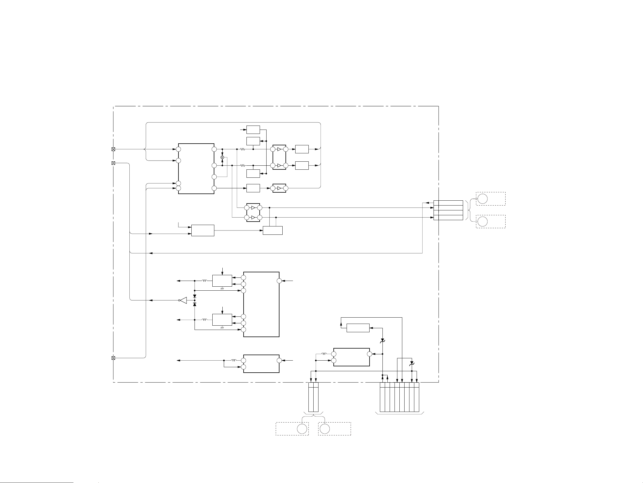
BLOCK DIAGRAM (5)
(EEPROM)WS60
H4
CN144
SDA-E
SCL-E
3
4
CN6022
TO G1 BOARD
1
2
EEPROM
IC141
S175
WE42/WE50
S195
WS60
S173 S172 S171 S174
+ PROG - PROG +
S193 S192 S191 S194
+ PROG - PROG +
(KEY INPUT,SIRCS)
H1
KF-WE42A1/WE50A1/WS60A1
RM-1022 RM-1022 RM-1022
CN191
WS60
WE42/WE50
CN171
KEY
2
22
–
22
–
TO G2 BOARD
CN6022
1
IC41
EEPROM
2
J40
3 4
21
V
4
L
J4302
i
L
(MONO)
R
CN44
SDA-E
3
SCL-E
4
CN2043
V4-V11
V4-C
9
V4-Y
7
5
V4-SSW
V4-L
3
1
V4-R
CN4302
HP SW
4
H.P (L)
3
H.P (R)
1
TO G2 BOARD
CN6022
I
TO UG BOARD
CN1502
B
TO AG BOARD
CN8002
(VIDEO 4 INPUT, EEPROM)WE42/WE50
H3
Q4504,4511
G
1
D4504
D4503
D4510
1
D6504
D6503
D6510
IC2171
REMOTE
CONTROL
RECEIVER
R
G
R
LED DRIVER
Q4509
LED DRIVER
Q6504,6511
LED DRIVER
Q6509
LED DRIVER
1
OUT
LED DRIVER
LED DRIVER
H2
LED DRIVER
LED DRIVER
Q4503,4510
Q4508
S4501
1
(POWER SWITCH)WE42/WE50
Q6503,6510
Q6508
1
2
IC2172
BUFFER
CN4502
STBY LED8
TIMER LED
7
6
LAMP-LED
5
GND
P-ON
4
STBY+3.3V
3
GND
2
POW_LED
1
+3.3V
STBY
5V
STBY +5V8
STBY LED
7
6
TIMER_LED
5
4
3
2
1
LAMP-LED
SIRLS
POW_LED
STBY
+3.3V
4
TO G2 BOARD
CN6021
TO G2 BOARD
CN6021
J2040
3 4
21
V
4
L
(VIDEO 4 INPUT)WS60
H3
J6302
i
L
(MONO)
R
CN2043
V4-V11
V4-C
9
V4-Y
7
5
V4-SSW
V4-L
3
1
V4-R
CN6302
HP SW
4
H.P (L)
3
H.P (R)
1
J
TO UG BOARD
CN1502
C
TO AG BOARD
CN8002
H2
(REMOTE CONTROL RECEIVER)WS60
– 31 –
– 32 –
Page 28
KF-WE42A1/WE50A1/WS60A1
RM-1022 RM-1022 RM-1022
BLOCK DIAGRAM (6)
STD/DUO
PRO
TO
G2 BOARD
CN6021
MS_BS
NC
MS_SDIO
MS_INS
MS_SCLK
VCC
STBY 3.3V
SIRCS
STBY 5V
CN2304
CN2302
2
3
4
6
8
9
+3.3V
STBY 3.3V
1
2
4
4
STBY 5V
WE42/WE50
IC2304
BUFFER
BUS BUFFER
1
2
IC2301
IC2303
Q2311
(ACCESS)
(
RECEIVER
16
3R
18
12
2RDEA
4
DO
14
4R
12
5D
IC2302
REMOTE
1
OUT
CONTROL
RECEIVER
Q2301,2302
(
LED DRIVER
+3.3V
120
1A1R
2
1B
3
2A
4
2B
5
3A
6
3B
7
4A
8
4B
9
5Y
10
5Z
+3.3VD
HMG(MEMORY STICK)
CN2301
THRU_3.3V
2
MS_BS+
4
MS_BS-5
7 MS_SDIR6 MS_SDIR+
9 MS_SCLK+
10 MS_SCLK12 MS_SDO+
13 MS_SDO15 MS_SDI+
16 MS_SDI17 MS_INS
19 MS_LED
CN2306
MS_3.3V
1
MS_3.3V
2
To
MS2C BOARD
D
TO AG BOARD
CN8202
TO A BOARD
CN6022
CN8001
LAMP COV
GND
T
(LAMP DOOR SWITCH)
S8001
(LAMP DOOR)
3
1
STD/DUO
PRO
TO
G2 BOARD
CN6021
CN5304
MS_BS
NC
MS_SDIO
MS_INS
MS_SCLK
VCC
CN5303
P-SW
GND
2
3
4
6
8
9
+3.3V
1
3
WS60
S5301
1
IC5301
RECEIVER
120
1A1R
2
1B
3
2A
4
IC5303
BUS BUFFER
DO
Q5311
(ACCESS)
(
16
18
12
4
14
12
(
3R
2RDEA
4R
5D
Q5301,5302
LED DRIVER
2B
5
3A
6
3B
7
4A
8
4B
9
5Y
10
5Z
HMG(MEMORY STICK)
+3.3V
+3.3VD
CN5301
THRU_3.3V
2
MS_BS+
4
MS_BS-5
7 MS_SDIR6 MS_SDIR+
9 MS_SCLK+
10 MS_SCLK12 MS_SDO+
13 MS_SDO15 MS_SDI+
16 MS_SDI17 MS_INS
19 MS_LED
CN5306
MS_3.3V
1
MS_3.3V
2
To
MS2C BOARD
E
TO AG BOARD
CN8202
– 33 –
– 34 –
Page 29
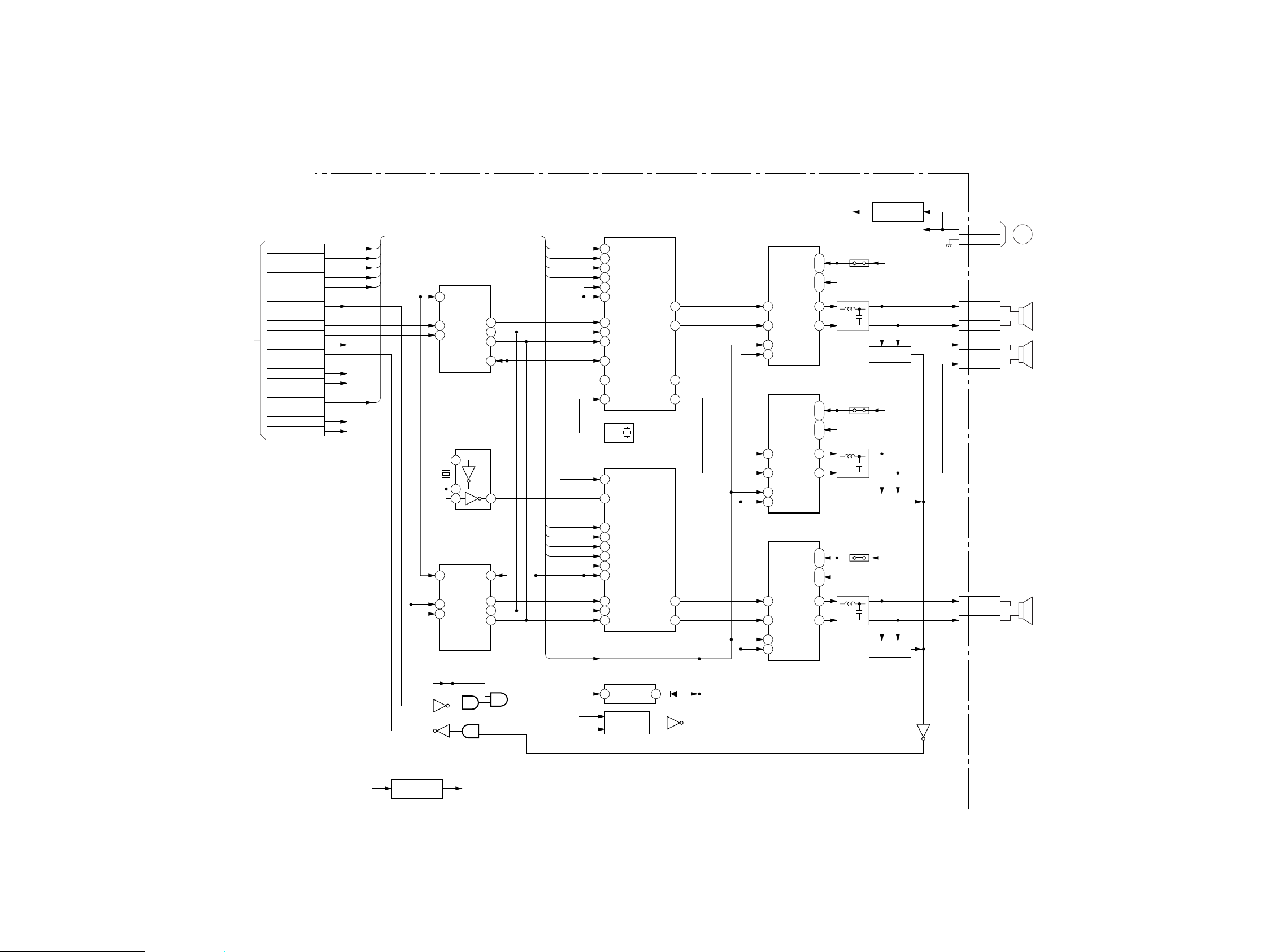
BLOCK DIAGRAM (7)
TO
G1 BOARD
CN6029
CN4703
RES_AMP
RST_PRO
SCDT
SCSHIFT
SLATCH-1
ADC-PD
SP-MUTE
L CH
R CH
AU-W
SP-DC-PROT
+5.0V
+3.3V
SLATCH-2
STBY 5V
DT +9V
9
10
11
12
13
14
15
17
19
21
23
24
25
30
39
40
MAIN-Y
INIT
SCDT
SCSHIFT
SLATCH-1
+5V
+3.3V
SLATCH-2
STBY+5V
+9V
+3.3V
IC4704
+
1.8V REG
+3.3V +1.8V
VCC OUT
X4702
Q4708
Q4711
IC4706
A/D CONVERTER
7 PDWN
1L IN
2R IN
IC4705
CLOCK 0SC
6
2
1 7
IC4701
A/D CONVERTER
7 PDWN
1W IN
2IN
IC4701
GATE
D OUT
BCK
LRCK
SCLKI
SCLKI
D OUT
BCK
LRCK
IC4701
(1/3)(2/3)
BUFFER
1/3
3/3
(3/3)
KF-WE42A1/WE50A1/WS60A1
RM-1022 RM-1022 RM-1022
IC4712
+
12V REG
+12V
IC4707
I2S-PWM CONVERTER
INIT
SCDT
SCSHIFT
SLATCH-1
27
19
16
15
INIT
SCDT
SCSHIFT
SLATCH-2
15
27
19
16
27 INIT
21 SCDT
22 SCSHFT
23 SLATCH
18 NSP MUTE
19 SOF MUTE
31 DATA
30 BCK
29
LRCK
36 XSFI IN
14 XSFO OUT
48 XSFO IN
OSC
X4703
OUT
49.152MHz
IC4702
I2S-PWM CONVERTER
48 XSF0 IN
36 XSFI IN
27 INIT
21 SCDT
22 SCSHFT
23 SLATCH
18 NSP MUTE
19 SOF MUTE
31 DATA
30 BCK
LRCK
29
OUT L1
OUT L2
OUT R1
OUT R2
OUT L1
OUT L2
11
9
6
4
11
9
RESET
IC4709
RESET DELAY
2/3
+3.3V
STBY+5V
+9V
VCC RESET
2 1
Q4901,4909
+B OFF
DETECT
D4717
Q4902
2BP
17 AP
4 /RST
13 /SD
2BP
17 AP
4 /RST
13 /SD
2BP
17 AP
4 /RST
13 /SD
IC4710
POWER AMP
PVDD_B
PVDD_A
OUT_B
IC4708
POWER AMP
PVDD_B
PVDD_A
OUT_B
IC4703
POWER AMP
PVDD_B
PVDD_A
OUT_B
32
.
31
24
.
23
30
25OUT_A
32
.
31
24
.
23
30
25OUT_A
32
.
31
24
.
23
30
25OUT_A
KD (AUDIO AMP)
PS4702
LPF
PS4703
LPF
PS4704
LPF
OUT VCC
AU+18V
AU+18V
DC DETECT
Q4706,4707
AU+18V
DC DETECT
Q4704,4705
AU+18V
DC DETECT
Q4701,4702
Q4703
1
2
1
2
3
4
1
3
CN4705
AU 18V
AU-GND
CN4702
L+
L-
R+
R-
CN4701
W+
W-
H
TO
G1 BOARD
CN1603
SP9001
SPEAKER
(
L-CH
SP9002
SPEAKER
(
R-CH
SP9003
SPEAKER
(
WOOFER
)
)
)
– 35 –
– 36 –
Page 30
KF-WE42A1/WE50A1/WS60A1
RM-1022 RM-1022 RM-1022
BLOCK DIAGRAM (8)
34
1
2
PR/C
PB/C
PR/C
PB/C
L
R
L
R
L
R
R
L
Y
R
L
Y
J1502
J9409
J1505
R
B
J1506
R
B
Y
L
R
Y
L
R
Y
L
R
VR
VB
VG
VR
VB
VG
CN1502
V4-VIN
V4-CIN
V4-YIN
V4-SSWIN
V4-LIN
V4-RIN
J1511
34
1
34
1
R
L
R
L
+
–
2
2
11
9
7
5
3
1
WE42/WE50
TO
H3 BOARD
CN43
WS60
TO
H3 BOARD
CN2043
1
(MONO)
2
(MONO)
3
(MONO)
1
2
I
J
V1-YJ1501
V1-CCY
V1-S
V1-V
V1-L
V1-R
V2-Y
T1501
V2-C
V2-S
V2-V
V2-L
V2-R
V3-Y
V3-C
V3-S
V3-V
V3-L
V3-R
V5-R
V5-L
V5-PR
V5-PB
V5-Y
V6-R
V6-L
V6-PR
V6-PB
V6-Y
V4-V
V4-C
V4-Y
V4-S
V4-L
V4-R
C-R
C-L
CY
CY
V1-V
V2-V
V3-V
V4-V
V1-Y
V2-Y
V3-Y
V4-Y
V1-C
V2-C
V3-C
V4-C
V1-S
V2-S
V3-S
V4-S
V6-PR
V6-PB
V6-Y
V5-PR
V5-PB
V5-Y
V6-PR
V6-PB
V6-Y
V1-L
V2-L
V3-L
V4-L
V5-L
V6-L
C-L
V1-R
V2-R
V3-R
V4-R
V5-R
V6-R
C-R
TEXT_PR
TEXT_PB
TEXT_Y
X1501
4MHz
12
17
22
13
18
23
14
19
24
11
16
21
42
41
40
35
34
33
51
11
16
14
19
13
10
16
20
14
11
17
IC1501
VIDEO INPUT SELECT
IN5_CV
IN6_CV
IN7_CV
7
IN4_CV
IN5_Y
IN6_Y
IN7_Y
8
IN9_Y
IN5_C
IN6_C
IN7_C
9
IN4_C
IN5_S
IN6_S
IN7_S
6
IN4_S
IN10_CR
IN10_CB
IN10_Y
IN9_CR
IN9_CB
IN9_Y
EXT_CLK/XTAL
IC1503
8
IN3A
IN2A
IN1A
IN3B
9
IN2B
IN1B
1
IC1502
AUDIO INPUT SELECT
IN7-L
IN5-L
IN4-L
IN3-L
7
4
IN2-L
1
IN1-L
IN6-L
IN7-R
IN5-R
IN4-R
IN3-R
8
IN2-R
5
IN1-R
2
IN6-R
CV/YOUT1
C/CBOUT1
CROUT1
CV/YOUT2
C/CBOUT2
CVOUT3
SEL_OUT1
SYNC_IN1
SDA
SCL
OUT3
OUT2
OUT1
SW1
SW2
SW3
SDA
SCL
LOUT1
ROUT1
LOUT2
ROUT2
IN8_L
IN8_R
IN9_L
IN9_R
IN10_L
IN10_R
12
58
59
60
67
68
71
56
55
79IN1_CV
1IN2_CV
77
76
74DC_OUT
6
5
3
2
7
32
31
39
37
35
33
22
23
25
26
28
29
V6-PR
V6-PB
V6-Y
SDA
SCL
SDA
SCL
MAIN-L
MAIN-R
MS_L
MS_R
MT L
MT_L
MT_R
Q1532
BUFFER
Q1513
BUFFER
Q1512
BUFFER
Q1511
BUFFER
Q1514
BUFFER
Q1518
BUFFER
Q1505, 1506
BUFFER
Q1524, 1502
BUFFER
Q1523, 1501
BUFFER
Q1516
BUFFER
Q1503
BUFFER
Q1508, 1510
MUTE
L OUT
R OUT
Q1507
MUTE DRIVE
MAIN-R
MAIN-L
TEXT-PR
TEXT-PB
TEXT-Y
MAIN-PR
MAIN-C/PB
MAIN-Y/CV
SUB_C/PB
SUB_CV
+5V
+9V
SCL
SDA
MT-R
MT-L
ST-L
MS-R
MS-L
L OUT
R OUT
NC
NC
NC
NC
NC
NC
NC
NC
CN1501
MAIN-R
50
MAIN-L
49
VAR/FIX-R
47
VAR/FIX-L
46
TEXT-PR
44
TEXT-PB
43
TEXT-Y
40
MAIN-PR
37
MAIN-C/PB
36
MAIN-Y
33
SUB-C
30
SUB-Y/CV
29
5V
28
5V
27
INS-C
25
INS-Y/CV
24
9V
22
SCLK-TV
20
SDAT-TV
19
SIRCS
18
MT-CV
15
MT-R
12
MT-L
11
STBY 5V
9
ST-CV
8
ST-L
7
MS-R
5
MS-L
4
MAMUAL
3
HDMI-RST
2
HDMI (AU) SW
1
J1504
VV OUT
L
R
L
R
A
TO
AG BOARD
CN8001
– 37 –
UG
– 38 –
(VIDEO INPUT)
Page 31

1
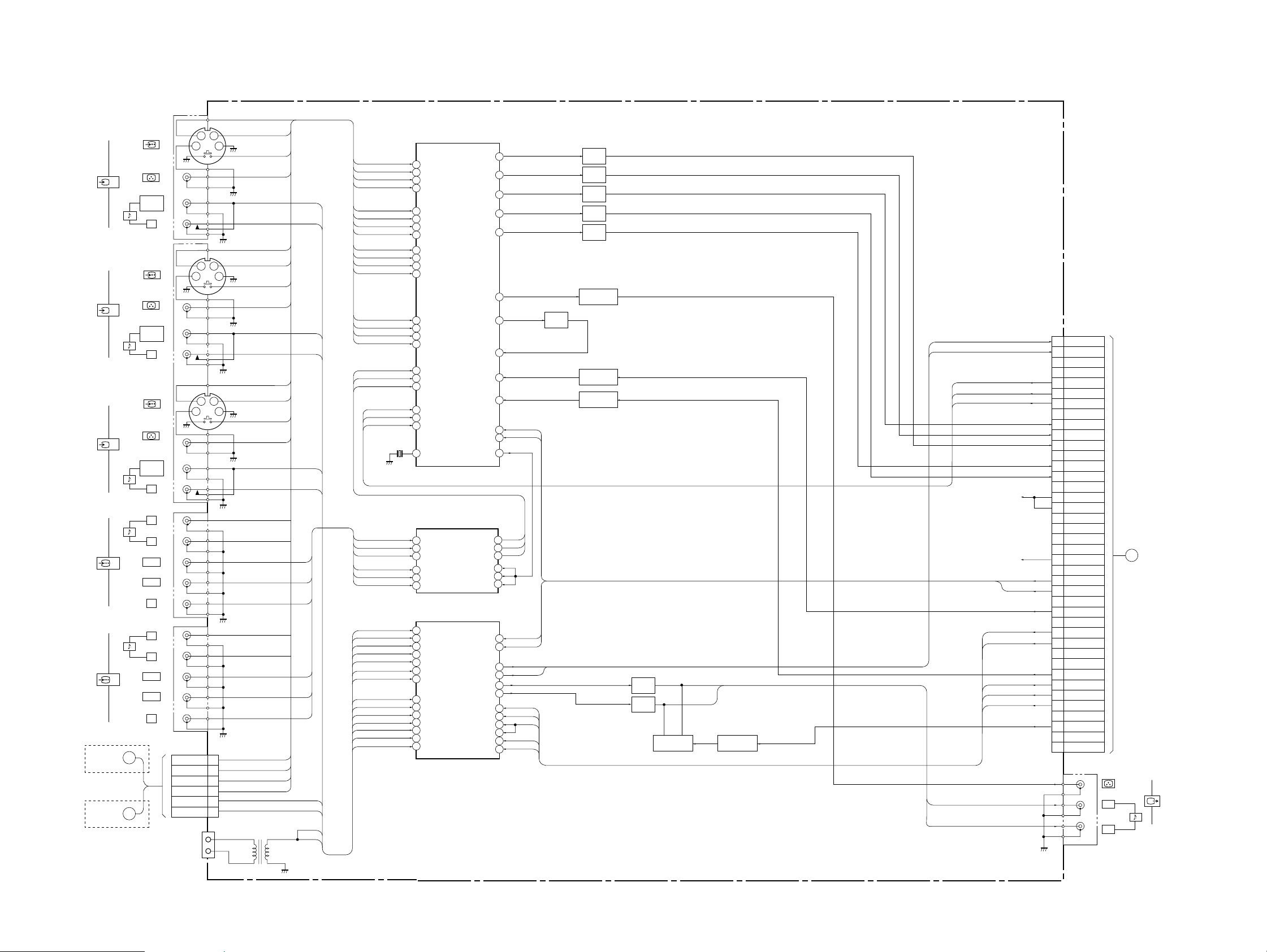
4-2. FRAME SCHEMATIC DIAGRAM
KF-WE42A1/WE50A1/WS60A1
RM-1022 RM-1022 RM-1022
A
B
C
D
1
2
43
98765
10
11
12
13
14
E
F
G
H
#
I
J
– 39 – – 40 –
Page 32

KF-WE42A1/WE50A1/WS60A1
1
RM-1022 RM-1022 RM-1022
A
B
C
D
1
2
43
98765
10
11
12
13
14
E
F
G
H
I
J
– 41 – – 42 –
Page 33

4-3. CIRCUIT BOARDS LOCATION 4-4. SCHEMATIC DIAGRAMS
KF-WE42A1/WE50A1/WS60A1
RM-1022 RM-1022 RM-1022
• KF-WE42M1/WE50M1
H1
G1
F
• KF-WS60M1
H1
G1
F
HMG
H2
MS2C
B
HMG
H2
T
H3
KD
A
C
Note:
• The parts marked “#” on schematic diagrams are not mounted.
• Capacitors without voltage indication are all 50V.
• All resistors are in ohms.
kΩ=1000Ω, MΩ=1000kΩ
• Indication of resistance, which dose not have one for rating electrical power, is
as follows.
Pitch : 5mm
Rating electrical power :
•
•
•
•
: nonflammable resistor.
: fusible resistor.
: internal component.
: panel designation and adjustment for repair.
1
/
W
4
• All variable and adjustable resistors have characteristic curve B, unless other-
Power supply
block
wise noted.
• : earth-chassis.
• Readings are taken with a PAL color-bar signal input.
RF splitter
• Readings are taken with a 10MΩ digital multimeter.
•Voltages are dc with respect to ground unless otherwise noted.
•Voltage variations may be noted due to normal production tolerances.
• All voltages are in V.
: Measurement impossibillity.
*
• Circled numbers are waveform references.
: B+ bus.
•
•
: B– bus.
•
: signal path.(RF)
UG
G2
Reference information
RESISTOR : RN METAL FILM
: RC SOLID
: FPRD NONFLAMMABLE CARBON
: FUSE NONFLAMMABLE FUSIBLE
: RW NONFLAMMABLE WIREWOUND
: RS NONFLAMMABLE METAL OXIDE
: RB NONFLAMMABLE CEMENT
ADJUSTMENT RESISTOR
:
KD
MS2C
B
T
COIL : LF-8L MICRO INDUCTOR
CAPACITOR : TA TANTALUM
A
H3
: PS STYROL
: PP POLYPROPYLENE
: PT MYLAR
: MPS METALIZED POLYESTER
: MPP METALIZED POLYPROPYLENE
: ALB BIPOLAR
: ALT HIGH TEMPERATURE
: ALR HIGH RIPPLE
C
Power supply
block
Terminal name of semiconductors in silk screen
printed circuit (
Device Printed symbol Terminal name
Transistor
1
Transistor
2
3
Diode
4
Diode
Diode
5
Diode
6
Diode
7
8
Diode
Diode
9
Diode
0
Diode
!¡
Diode
!™
Transistor
!£
(FET)
Transistor
!¢
(FET)
Transistor
!∞
(FET)
Transistor
!§
Transistor
!¶
Transistor
!•
Transistor
!ª
Transistor
@º
Transistor
@¡
Transistor
@™
Transistor
@£
Discrete semiconductot
–
(Chip semiconductors that are not actually used are included.)
)
*
Collector
Base
Collector
Base
Cathode
Cathode
Anode
Cathode
Anode
Common
Anode
Common
Anode Cathode
Common
Anode
Common
Anode Anode
Common
Cathode
Common
Cathode
Anode
Anode
Cathode
Drain
Drain
B1 E1
C2
B2 C1
E2
B2 E2
C1
B1 C2
E1
B2 E2
C1
B1 C2
E1
B2 E2
C1
B1 C2
E1
E2
B1 E1
C2
(B2)
E1
B1
C1
(B2)
E1
E2
C2
Emitter
Emitter
Anode
(NC)
(NC)
Cathode
Anode
Cathode
Cathode
Cathode
Anode
Anode
Source
Gate
Source
Gate
Source
Drain
Gate
Emitter
Collector
Base
C1(B2)
E2
C2
B1
C1
Circuit
D
G
G
S
D
S
D
G
S
C2
C1
B1
E1
E2
C2
C1
B1
E1
E2
E2
E1
B1
C1
C2
B1
B1
B1
C2C1(B2)
E2
E2
E2E1(B2)
C1
C2
C2E1(B2)
C1
C2
D
S
G
B2
B2
B2
Ver.1.5
RF splitter
display is on the component slde.
H4
G2
UG
Note: The symbol
The components identified by shading and mark
are critical for safety. Replace only with part number
specified.
The symbol
indicate fast operating fuse.
Replace only with fuse of same rating as maked.
– 43 – – 44 –
Page 34

KF-WE42A1/WE50A1/WS60A1
1
RM-1022 RM-1022 RM-1022
1
2
3
4
(1) AG (1/5) Board
1
A
B
N8001
C
50P
TO B
:B
C
D
E
1.6 Vp-p (H)
2
43
98765
1.6 Vp-p (H)
10
4.2 Vp-p (H)
11
4.2 Vp-p (V)
12
13
14
TU8002
IC
R
C8030
0.047
16V
B:1608
:R
C8036
CH
8001
ESET
C8035
6.3V
B:1608
8049
R
6.8k
1/10W
N
150p
:1608
1
-CP
BTF-LG434(40)
A
SU
C8029
CH
R8044
1M
1/10W
:C
R
1/10W
:CH
330p
HIP
8050
10k
B-TU
:1608
IP
R8038
R
1/10W
:CH
#
8048
10k
R
1/10W
:CH
IP
1.5k
8037
8019
R
100
1/10W
:CH
IP
8001
C
L8007
M
SD
BU
C8009
100
16V
L-CP
:A
C8021
470p
B:1608
Q8012
601-RT1
FFER
8075
R
470
1/10W
:CH
#
IP
R
1/10W
:CH
R8008
:1608
8076
1.5k
0
IP
C8010
#
8026
R
100
1/10W
:CH
#
R8009
:CHIP
1/10W
100
IP
R8027
SCL
SDA
8004
R
0
:1608
R8007
0
8016
R
:1608
#
8012
R
#
8017
R
8020
C
#
0
:1608
ST-L
8025
R
2.2k
1/10W
:CH
Q8004
SB
M
BUFFER
ST_VIDEO
C8023
#
IP
709-RT1
8042
R
100
1/10W
:CH
R
:1608
R
IP
8032
8033
0
#
SAFT
IP
L8004
L8018
L8006
C8002
:AL-C
C8011
:A
C8017
100
16V
:AL-CP
100
16V
47
L-CP
P
C8003
470p
:1608
B
C8016
470p
B:1608
C8022
470p
B:1608
+9V
+33V
+5V
CN
C
8005
1P
N8006
1P
TU8001
M
D
D
M
M
8001
L914T1
+3.3V
8006
Q
SB709-R
FFER
BU
S-80843CLU
T1
S-HSYNC
C8007
100
16V
L-CP
:A
8006
C
L8001
0.0022
B:1608
TE
U
L-M
W
V-S
YU
ST
I-R
M
D
H
L
R
T-L
S
T_VIDEO
S
Y5V
STB
T-L
M
T-R
M
CS
SIR
+9V
+5V
Y/CV
C
IIC-TV
SD
SCL
B-CV/YC-O
SU
A
8028
R
0
:1608
C8027
0.0022
:1608
B
8043
R
6.8k
1/10W
N
:R
8033
C
150p
:1608
CH
UT
M-HSYNC
LZ06
:LH
8005
C
0.0022
B:1608
:CHIP
:CHIP
R8018
#
1/10W
1/10W
100
100
L8003
C8019
C8018
0.0022
B:1608
C8028
100
16V
L-CP
:A
C8032
B:1608
-CP
8045
R
10k
1/10W
-CP
N
:R
:AL-C
6.3V
100
16V
M
SEPAR
1
P
8005
Q
SB709-RT1
C.
SYN
ATOR
:LH
L8008
LZ06
:LHLZ06
8046
R
10k
1/10W
N-CP
:R
R8020
SCL
R8021
SDA
#
R8023
8004
C
8002
R
#
#
8001
Q
#
8073
R
470
1/10W
IP
:CH
C8025
470
16V
:AL-CP
8002
D
#
OT
PR
C8031
R8040
0.047
150k
16V
-CP
N
:R
B:1608
8047
R
1M
1/10W
AGC
N-CP
:R
R
R
:1608
8013
#
R
SD
M
R
1/10W
:C
C8026
0.0022
B:1608
C8034
CH
8010
0
8014
#
8011
Q
601-R
8074
1.5k
HIP
R8031
2.2k
1/10W
:CH
330p
:1608
8005
R
#
8003
R
#
8008
C
L8002
#
T1
8022
R
#
IP
8041
R
1.5k
1/10W
-CP
N
:R
MAFT
8012
C
100
16V
:AL-CP
R
:1608
M
8034
0
8002
Q
SB709-R
UFFER
B
8013
C
0.1
25V
F:1608
8024
R
SDA
8030
R
100
1/10W
:CH
#
8036
R
0
:1608
IP
I-SAP
8029
R
100
1/10W
IP
:CH
T1
SCL
C8014
6.3V
B:1608
JR8001
#
8001
R
#
8006
R
#
8002
JR
0
:1608
8015
C
1
1
MT-R
MT-L
B
6.3V
:1608
R8039
150k
1/10W
:CH
IP
F
G
H
8007
+3.3V
:S-M
:S-M
CN
#
8002
CN
5P
T
H
W
O
ICR
8003
CN
3P
T
H
W
O
ICR
8008
N
C
6P
B
TO
:B
Y
+3.3V
8080
R
47k
1/10W
IP
:CH
C8069
#
16V
B:1608
TE
U
-M
VAR
+9V
+11V
L8017
L8016
470
16V
:LH
P
TEXT_Y
TEXT_PB
TEXT_PR
PB
PR
-LR
AIN
M
L
R
+3.3V
+2.5V
6V
D
D
R
27k
1/10W
:CH
8015
Q
2PB709AR
UTE-SW
M
082
R
18k
1/10W
IP
:CH
083
IP
DD OVP
M
R
:1608
R
D
M
U
084
0
8006
113
A
TE-SW
Q
TC114EKA
D
U
M
L
8016
TE-SW
085
R
47k
1/10W
:CH
IP
FM
+9V
O
N
O
S-HSYNC
M-HSYNC
C8072
:AL-C
MAFT
R
:1608
M
4.7
M
086
0
M
SAFT
D
U
P
8008
L914T1
D
TE-SW
AGC
R
1M
1/10W
:CH
8007
D
C8071
A113
M
100
ECT
R
16V
:AL-CP
Q8017
2PB709AR
TE-SW
U
087
R
22k
1/10W
IP
H
:C
088
IP
I-SAP
8009
D
A152W
1M
M
TE
U
M
SCL
SDA
PR
M
A
P
M
BCO
SU
Y
Y
PB
PR
PB
VD
HD
SIRCS
HDMI-RST
YUV-SW
L8014
STBY5V
L8015
C8067
:AL-C
I
M
LZ06
SD
Q8014
601-R
IN
8077
R
10k
1/10W
IP
:CH
R8079
10k
1/10W
IP
:CH
T1
V.
+5V
C8068
470
16V
P
:AL-C
R8081
1/10W
:CHIP
WF
#
8078
R
10k
1/10W
IP
:CH
C8070
#
16V
8013
Q
601-R
SD
M
V.
IN
L
R
B:1608
T1
8051
R
4.7k
P
H
AU
C8046
0.1
25V
F:1608
R
1/10W
T
U
O
IO
D
L8011
+5V
8055
R
2.2k
1/10W
IP
:CH
8060
R
470
8062
10k
IP
:CH
1/10W
IP
:CH
8010
Q
SD
M
601-R
V.
IN
TEXT-BLK
G
D
D
D
R
T1
D
N
+1.8V
8005
D
5.6SB3-T1
C8049
0.1
16V
B:1608
C8044
0.1
16V
B:1608
+9V
C8045
:AL-C
8061
R
220
1/10W
:CH
L8010
100
16V
IP
P
L
ND
G
R
D
ZSTE-1718B
D
U
8004
8004
CN
96P
B
:B TO
J
– 46 –– 45 –
Page 35

(2) AG (2/5) Board
5
0.3 Vp-p (62nsec)
6
4.8 Vp-p (V)
7
4.8 Vp-p (H)
KF-WE42A1/WE50A1/WS60A1
RM-1022 RM-1022 RM-1022
A
B
C
D
E
F
G
H
R8254
1/10W
:CHIP
C8202
0.1
16V
B:1608
X8201
C8256
0.1
16V
B:1608
C8259
0.1
16V
B:1608
SUBCOMP
R8243
1/10W
10k
:AL-CP
:CHIP
C8221
220
B:1608
10
C8248
0.1
16V
R8266
10k
1/10W
:CHIP
10
R8267
1/10W
:CHIP
C8236
B:1608
Q8218
2SA1576A-T106
Q8220
2SC4081T
R8257
470
1/10W
:CHIP
C8249
#
10V
100
D
V
0.1
16V
R8275
1/10W
R8258
100
1/10W
:CHIP
C8234
0.01
25V
B:1608
IC8202
CXA2163AQ-T6
SUB COLOR
DECODER
C8257
0.01
25V
B:1608
R8268
100
1/10W
:CHIP
100
C8203
0.01
25V
B:1608
D
H
C8252
11
JR8201
#
R8239
47
1/10W
:CHIP
C8214
0.1 16V
C8216
C8215
0.1
0.1
16V
16V
#
25V
C8254
#
C8253
#
R8272
100 1/10W
TEXT_H
TEXT_V
FB8206
FB8207
R8262
1/10W
:CHIP
0
0
12
Q8204
DTC114U
SWITCH
BLK
TEXT_R
TEXT_G
TEXT_B
R8229
100
1/10W
:CHIP
R8232
100
1/10W
:CHIP
R8234
100
1/10W
:CHIP
C8239
4.7
:AL-CP
R8259
100
1/10W
:CHIP
100
R8250
100
1/10W
R8261
100
1/10W
IC8203
TC7SET02FU
GND
R8240
100+1/10W
R8244
470
1/10W
Q8219
MSB709-RT1
BUFFER
R8252
470
1/10W
Q8222
MSB709-RT1
BUFFER
VCC
TEXT-BLK
Q8210
MSB709-RT1
BUFFER
R8236
470
1/10W
R8321
:1608
Q8216
MSB709-RT1
BUFFER
R8322
:1608
R8278
180
1/10W
0
SDA
SCL
R8256
1/10W
0
82
13
R8213
470
1/10W
:CHIP
Q8212
MSB709-RT1
BUFFER
C8260
470p
50V
R8214
1/10W
:CHIP
R8263
1/10W
470
R8247
1/10W
820
14
TO AG 2/5,5/5_16
R8320
470
1/10W
:CHIP
PB
PR
Y
Q8214
MSB709-RT1
BUFFER
TEXT_PR
TEXT_PB
+5V
1k
TEXT_Y
R8323
0
:1608
Q8221
MSB709-RT1
BUFFER
25V
47
C8244
:AL-CP
25V
C8207
B:1608
47
0.01
25V
C8223
25V
+9V
B:1608
R8233
:1608
C8238
0.01
25V
B:1608
C8241
0.01
25V
B:1608
R8269
470
1/10W
:CHIP
MSB709-RT1
0
43
L8219
Q8224
BUFFER
FB8202
BK1608HS601
C8313
:AL-CP
R8270
1/10W
:CHIP
47
1k
IC8201
TC90A69F
:B2H
C8312
0.1
16V
B:1608
Q8223
MSD601-RT1
BUFFER
R8277
100
1/10W
:CHIP
MSB709-RT1
Q8226
BUFFER
R8271
1/10W
:CHIP
Q8202
2SA1576A-T106
R8201
12k
1/10W
R8206
1.2k
1/10W
:CHIP
C8204
B:1608
R8211
1/10W
:CHIP
C8217
:AL-CP
R8223
1.2k
1/10W
:CHIP
IIC-TV
:CHIP
0.1
16V
R8207
6.8k
1/10W
:CHIP
12k
47
25V
Q8201
2SC4081T
R8204
820
L8202
1/10W
:CHIP
C8206
C8205
R8205
1k
1/10W
:CHIP
Q8206
2SC4081T
C8208
0.01
25V
B:1608
C8218
0.01
25V
B:1608
R8222
1k
:CHIP
:CHIP
1/10W
:CHIP
C8224
0.1
16V
B:1608
C8228
B:1608
C8231
L8205
:CHIP
:AL-CP
Q8225
MSD601-RT1
BUFFER
R8276
1k
1/10W
:CHIP
100
100
R8221
330
1/10W
:CHIP
C8227
680p
B:1608
R8251
1/10W
R8255
1/10W
470
R8274
470
1/10W
:CHIP
0.1
16V
100
16V
22p
CH:1608
CH:1608
R8215
1/10W
:CHIP
C8219
22p
12p
CH:1608
820
L8204
C8220
12p
CH:1608
SDA
SCL
R8220
6.8k
1/10W
:CHIP
Q8208
2SC4081T
+9V
C8316
B:1608
R8202
1k
1/10W
:CHIP
R8208
390
1/10W
:CHIP
R8212
1k
1/10W
:CHIP
R8224
470
1/10W
:CHIP
0.1
16V
C8232
0.01
25V
B:1608
C8235
10V
F:1608
1
Q8203
2SC4081T
R8209
1/10W
Q8207
2SA1576A-T106
R8219
470
1/10W
:CHIP
IC8207
BA05FP-E2
+5V REG.
:CHIP
R8203
470
:1608
0
Q8205
2SC4081T
R8210
0
:1608
R8216
1k
1/10W
:CHIP
Q8209
2SC4081T
R8225
0
:1608
R8238
4.7M
1/10W
:CHIP
C8250
1
10V
F:1608
R8230
1k
1/10W
:CHIP
A5V
R8264
0
:1608
C8318
C8317
B:1608
47
0.1
16V
25V
:AL-CP
1
Y/CV
C
I
SUB-CV/YC-OUT
R8235
100
1/10W
:CHIP
Q8215
2SC4081T
BUFF
R8248
1/10W
:CHIP
C8242
15p
CH:1608
R8279
2.2k
1/10W
Q8227
MSB709-RT1
BUFFER
R8281
100 1/10W
2
L8220
C8314
C8315
0.1
47
16V
:AL-CP
B:1608
C8209
0.01
25V
B:1608
Q8211
2SC4081T
R8217
470
1/10W
:CHIP
R8226
390
1/10W
:CHIP
R8227
1/10W
:CHIP
Q8213
2SA1576A-T106
470
R8246
560
1/10W
:CHIP
R8249
5.6k
1/10W
:CHIP
FL8201
R8280
100
1/10W
C8213
0.01
25V
B:1608
C8211
0.1
16V
B:1608
C8210
100
16V
:AL-CP
0.01
C8226
1k
0.47
10V
B:1608
L8203
:CHIP
L8206
:CHIP
C8237
:AL-CP
L8207
:CHIP
FB8203
BK2125HM601
+5V
R8265
470
1/10W
:CHIP
R8273
100
1/10W
:CHIP
TEXT_CV
R8241
1/10W
:CHIP
C8245
0.01
25V
B:1608
47
C8229
0.47
B:1608
C8240
:AL-CP
C8243
100
CH:1608
FB8204
FB8205
10V
2.2
:1608
:1608
A5V
C8230
10V
0
0
98765
R8242
22k
1/10W
:CHIP
R8253
100
1/10W
:CHIP
C8247
#
FB8201
C8201
47
0
25V
:1608
:AL-CP
L8201
C8212
10p
CH:1608
C8222
#
25V
C8225
0.01
25V
B:1608
R8228
27k
1/10W
:CHIP
#
R8245
10k
1/10W
:RN-CP
C8246
0.01
25V
B:1608
R8260
4.7M
1/10W
:CHIP
C8255
47
25V
:AL-CP
L8208
L8209
C8258
470
16V
:AL-CP
J
– 47 – – 48 –
Page 36

KF-WE42A1/WE50A1/WS60A1
1
RM-1022 RM-1022 RM-1022
(3) AG (3/5) Board
A
B
C
D
E
F
G
H
1
2
43
98765
10
11
12
13
14
CN8202
4P
R8295
18k
1/10W
C8273
0.0033
B:1608
C8309
0.0022
B:1608
R8319
27k
1/10W
:RN-CP
L8212
:CHIP
WHT
:S-MICRO
C8271
470
16V
:AL-CP
C8310
10V
B:3216
IC8204
PQ1CZ41H2ZPH
+1.8V REG.
R8282
R8284
#
510
C8268
0.001
D8207
D8209
#
#
C8267
:AL-CP
470
16V
L8213
:CHIP
C8277
C8300
L8217
:CHIP
B:1608
82
16V
82
16V
DD 6V
R8288
0
:1608
DDGND
C8263
100
16V
:AL-CP
D8204
M1FM3
C8275
R8298
0.1
10
16V
1/10W
B:1608
:CHIP
R8308
100k
1/10W
:CHIP
C8303
0.1
16V
B:1608
D8214
M1FM3
C8311
10
10
25V
B:3225
C8286
25V
B:CHIP
R8312
1/10W
:CHIP
C8261
16V
B:CHIP
0.1
10
C8262
10
#
B:1608
C8276
10
25V
B:3225
R8303
6.8k
1/10W
:CHIP
C8307
C8308
10
25V
:1608
B:3225
RB063L-30TE25
C8282
#
:1608
#
D8201
IRF7335D1-TR
SWITCHING
C8292
B:CHIP
IRF7335D1-TR
SWITCHING
Q8229
0.1
25V
Q8233
L8211
:CHIP
R8307
6.8k
1/10W
:CHIP
C8264
0.1
16V
B:CHIP
C8283
:1608
C8295
:1608
#
#
1/10W
:RN-CP
R8285
1/10W
:RN-CP
C8278
16V
B:1608
C8304
0.1
16V
B:1608
1/10W
:RN-CP
1k
L8214
:CHIP
C8279
1000
6.3V
:AL-CP
0.1
C8301
1000
6.3V
:AL-CP
L8218
:CHIP
C8280
B:1608
C8302
B:1608
#
#
D8200
RTZ-TE25-3.9B
D8205
UDZS-4.3B
R8302
1/10W
:CHIP
R8310
1k
1/10W
:CHIP
MMDL914T1
D8213
UDZS-4.3B
+1.8V
D8206
MMDL914T1
1k
D8210
+3.3V
+2.5V
R8304
1/10W
:CHIP
DD OVP
Q8232
2PD601AR
C8285
#
B:1608
R8237
1k
1/10W
:CHIP
10k
C8296
:1608
CN8201
B14B-XADSS-N-A
R8314
1k
1/10W
:CHIP
D8212
MMDL914T1
PROT
D8211
MM3Z5V6ST1
MS3.3V OVP
R8292
2.2k
1/10W
:CHIP
C8294
#
D8208
DUMPER
L8215
:LHL13
C8287
:1608
R8300
22k
1/10W
:CHIP
R8299
3.3k
1/10W
:CHIP
C8290
470
16V
C8289
0.1
25V
F:1608
L8216
#
C8288
1000
6.3V
:AL-CP
R8305
1/10W
:CHIP
R8313
1/10W
:CHIP
33
1k
R8289
270k
1/10W
:CHIP
R8306
120k
1/10W
:CHIP
R8311
100k
1/10W
:CHIP
2SC2412K
C8281
0.1
16V
B:1608
C8284
47p
CH:1608
C8291
0.1
16V
B:1608
R8309
100k
1/10W
:CHIP
Q8231
SW
D8202
UDZS-TE17-5.6B
D8215
DINL20U-TA2
IC8206
S18033JF
3.3V
REG
L8221
#
C8297
10000
16V
C8298
0.1
25V
F:1608
EC21QS04-TE12L
R8293
10k
1/10W
:RN-CP
D8203
C8299
0.1
16V
B:1608
R8317
10k
1/10W
:RN-CP
#
B:1608
R8315
680
1/10W
:CHIP
R8296
1/10W
:CHIP
B:1608
C8293
0.1
16V
680
C8272
C8274
0.033
16V
R8291
10k
1/10W
:CHIP
Q8230
2SC2412K
SW
R8301
10k
1/10W
:CHIP
R8294
1/10W
:RN-CP
R8297
1/10W
:CHIP
#
C8305
0.033
16V
B:1608
C8270
82
16V
3.3k
330
C8306
#
R8318
3.3k
1/10W
:RN-CP
R8316
1/10W
:CHIP
330
:RN-CP
IC8205
TPS5120DBTR
SWITCHING
REGULATOR
I
J
– 50 –– 49 –
Page 37

(4) AG (4/5) Board
KF-WE42A1/WE50A1/WS60A1
RM-1022 RM-1022 RM-1022
A
B
C
D
E
F
G
H
:CHIP
:CHIP
10
C8430
47
25V
:AL-CP
C8435
47
25V
:AL-CP
V
.3
+3
10
16V
R8493
1/10W
12k
:CHIP
R8489
1/10W
:CHIP
Q8414
#
R8481
0
:1608
R8483
#
22k
R8494
2.2k
1/10W
:CHIP
IC8405
NJM4558V-TE2
LPF
R
R8476
#
Q8415
#
C8452
:AL-CP
22k
22k
R8455
68
R8469
68
2PD601AR
BUFFER
Q8416
R8508
1/10W
:CHIP
R8512
4.7k
1/10W
:CHIP
R8477
2.2k
R8498
1/10W
:CHIP
R8501
1/10W
:CHIP
#
39k
22k
R8495
39k
1/10W
:CHIP
+9V
R8456
470k
R8463
2.2k
R8464
R8471
470k
11
10k
R8479
C8463
0.0..
:MPS
#
R8491
#
:1608
C8480
0.1
16V
B:1608
C8489
100p
CH:1608
C8491
16V
:AL-CP
R8492
1/10W
:CHIP
R8500
100
1/10W
:CHIP
C8466
CH:1608
R8502
47k
1/10W
:CHIP
R8513
1/10W
:CHIP
#
#
#
#
Q8412
MSD601-RT1
MUTE
Q8413
MSD601-RT1
MUTE
C8474
R8507
1/10W
:CHIP
C8481
100
16V
:AL-CP
:MPS
12
HP
L
R
GND
F
W
R8497
R8503
0
#
:1608
:1608
C8467
0.0..
:MPS
#
V
+9
#
L8402
:FLR50
R8511
1k
1/10W
:CHIP
R8514
0
:1608
13
14
Q8411
HPF
MSD601-RT1
R8412
1k
1/10W
:CHIP
R8424
22k
1/10W
:CHIP
1M
Q8401
BIAS
C8410
100
16V
:AL-CP
43
C8414
10p
CH:1608
+9V
M1MA152WA
L-MUTE
D8405
MUTE
C8422
47
25V
:AL-CP
C8420
0.1
16V
B:1608
C8427
CH:1608
Q8403
2PB709AR
MUTE-SW
R8438
180k
1/10W
:CHIP
10p
C8412
47p
CH:1608
R8418
1.5k
1/10W
:CHIP
C8424
47p
CH:1608
L
R8413
0
:1608
NJM4558V-TE2
R8441
1/10W
R8446
0
:1608
R8504
0
:1608
CH:1608
R8417
1/10W
:CHIP
IC8402
FILTER-W
4.7k
:CHIP
C8425
47p
CH:1608
4.7k
C8409
47p
R8499
20k
1/10W
:CHIP
0.022
1000p
22000p
680p
0.15
C8464
C8468
C8472
C8475
C8426
0.047
C8461
25V
C8470
C8416
0.047
:MPS
L
C8453
0.01
25V
B:1608
:MPS
:MPS
MAIN-LR
C8457
0.22
16V
B:1608
B:1608
:PT
:MPS
:PT
R8443
1/10W
:CHIP
R
IIC-TV
15k
R8449
1/10W
:CHIP
100
98765
+9V
R8420
15k
1/10W
:CHIP
Q8404
MSD601-RT1
BUFFER
R8429
0
R8432
R8431
3.3k
15k
1/10W
1/10W
:CHIP
:CHIP
Q8409
MSD601-RT1
BUFFER
R8450
1/10W
:CHIP
C8454
B:1608
:AL-CP
C8477
B:1608
R8447
R8485
6.8k
1/10W
:CHIP
C8482
0.33
10V
B:1608
C8440
:AL-CP
C8442
:AL-CP
0
C8447
0.22
16V
10
B:1608
16V
C8445
0.22
16V
B:1608
C8444
0.22
10
16V
16V
B:1608
C8483
1
:AL-CP
C8484
1
:AL-CP
R8515
22
1/10W
:CHIP
+9V
3.3k
0.22
16V
0.22
16V
15k
R8484
2.2k
1/10W
:CHIP
R8486
2.2k
1/10W
:CHIP
R8487
6.8k
1/10W
:CHIP
C8455
0.0047
B:1608
R8496
20k
1/10W
:CHIP
16V
SDA
SCL
AUDIO OUT
R8451
C8429
22
3.9k
16V
47k
R8466
1/10W
:CHIP
C8487
:AL-CP
47k
C8434
10V
B:1608
16V
C8488
:AL-CP
1
1
C8437
R8478
R8488
1/10W
1
:CHIP
:AL-CP
20k
:AL-CP
C8451
0.0047
B:1608
R8473
3.9k
1/10W
:RN-CP
#
C8438
100
16V
:AL-CP
1/10W
:RN-CP
M1MA152WK
M1MA152WA
C8428
1
10V
B:1608
C8485
4.7
:AL-CP
C8443
0.01
25V
B:1608
C8493
1000
16V
0.0047
C8486
1
:AL-CP
D8407
HZU11B1
PROTECT
C8446
B:1608
R8457
1/10W
:CHIP
22
R8482
12k
1/10W
L
R
C8448
0.22
C8449
16V
C8450
0.22
B:1608
R8516
1/10W
:CHIP
22
16V
B:1608
IC8404
NJW1149
C8490
B:1608
C8492
1000
16V
0.1
16V
L8403
:LAV35
0.22
16V
B:1608
R8474
22k
1/10W
:CHIP
D8408
D8409
R8480
1/10W
10k
C8479
:AL-CP
R8452
1/10W
R8490
1/10W
:CHIP
0.01
C8462
:AL-CP
1
R8444
#
22k
R8453
0
IC8403
NJM4560M
C8436
0.1
25V
F:1608
20k
C8456
B:1608
25V
C8458
0.0047
C8459
0.0047
C8460
1
:AL-CP
1
C8465
C8469
1000p
22000p
680p
C8476
0.15
C8478
#
16V
B:1608
B:1608
C8471
C8473
B:1608
:MPS
R8509
1/10W
:CHIP
+9V
L8401
C8433
100
16V
:AL-CP
R8475
0
1
:AL-CP
:PT
:MPS
:PT
R8506
1/10W
#
R8510
1/10W
1
R8408
#
L
R
R8415
1/10W
:CHIP
2
R8427
0
R8422
R8421
:1608
C8418
C8417
R8428
0
0.15
0.033
:1608
:MPS
:MPS
R8433
1.2k
1/10W
:CHIP
R8461
0
R8472
#
B:1608
2PB709AR
MUTE-SW
R8411
18k
27k
1/10W
:CHIP
R8423
0
:1608
R8460
1/10W
:CHIP
C8407
0.1
16V
Q8402
1.5k
R8462
0
:1608
R8470
180k
1/10W
:CHIP
R8404
6.8k
1/10W
:CHIP
C8402
10
16V
:AL-CP
Q8405
DTC114EKA-T146
MUTE-SW
VAR-MUTE
R8434
1/10W
:CHIP
#
47k
C8431
0.15
:MPS
R8465
1/10W
:CHIP
1.2k
MUTE-SW
D8401
MA113
C8432
0.033
:MPS
R8458
:1608
R8467
1/10W
:CHIP
R8416
1/10W
:CHIP
47k
47k
390
1/10W
:CHIP
Q8406
MSD601-RT1
R8435
5.6k
1/10W
:CHIP
#
HPF
R8409
3.3k
1/10W
:CHIP
R8414
0
:1608
MMDL914T1
C8415
4.7
:AL-CP
R8459
390
1/10W
:CHIP
MSD601-RT1
R8468
5.6k
1/10W
:CHIP
D8402
MA113
D8403
MUTE-SW
R8426
1/10W
RECT
:CHIP
I
J
– 51 – – 52 –
Page 38

KF-WE42A1/WE50A1/WS60A1
RM-1022 RM-1022 RM-1022
(5) AG (5/5) Board
A
B
C
D
E
F
G
H
1
2
43
98765
10
11
12
8
3.0 Vp-p (83.7nsec)
R8624
100
1/10W
C8620
0.1
16V
C8619
D8601
#
R8601 47k 1/10W
R8602 100 1/10W
R8603
100
1/10W
X8601 12MHZ
C8605
C8604
56p
56p
50V
50V
R8618
1/10W
C8615
50V
FB8604
75
MSD601-RT1
FB8603
0
4.7
C8616
#
0
R8619
75
1/10W
R8634
100
1/10W
IC8601
SAA5360HL
C8614
0.1
16V
R8628
24k
0.1
1/10W
16V
C8618
4.7
50V
R8629
1/16w
C8617
0.1
16V
220
C8601
16V
Q8601
R8606
0.1
INV.
0
R8620
1/10W
R8608
100 1/10W
C8606
FB8602
4.7 50V
0
R8612
100 1/10W
R8613
1/10W
:CHIP
R8621
100
1/10W
R8626
470
1/10W
R8631
100
1/10W
Q8607
MSB709-RT1
BUFFER
1k
R8615
470 1/10W
C8607
0.1
16V
IC8603
PST9129NL
RESET
Q8609
MSB709-RT1
BUFFER
MSB709-RT1
MSB709-RT1
R8627
1/10W
Q8604
BUFFER
Q8605
BUFFER
330
R8635
1/10W
470
R8607
#
1/10W
:CHIP
R8632
470
75
1/10W
C8611
R8616
1/10W
R8623
330
1/10W
0.1
16V
330
D8602
DAP202K
FMONO
C8612
100
16V
Q8603
MSD601-RT1
BUFFER
R8610
100 1/10W
C8613
16V
:RN-CP
:RN-CP
0.1
R8617
1/10W
:RN-CP
R8625
1/10W
R8630
1/10W
SDA
SCL
IIC-TV
IC8602
NJM2870F33
+3.3V REG.
R8604
12
FB8601
1W
0
R8609
10k
1/10W
TEXT_V
R8611
0
R8637
100
1/10W
BLK
R8636
470
1/10W
TEXT_H
R8622
180 1/10W
TEXT_R
TEXT_G
TEXT_B
Q8606
MSD601-RT1
BUFFER
#
#
#
C8602
16V
C8603
0.1
100
16V
TO AG 2/5,5/5_16
R8633
100 1/10W
JR8601
#
+5V
TEXT_CV
I
J
– 54 –– 53 –
Page 39

(6) B (1/6) Board
1
A
B
C
KF-WE42A1/WE50A1/WS60A1
RM-1022 RM-1022 RM-1022
2
43
98765
10
11
12
13
14
D
E
F
G
H
I
J
– 55 – – 56 –
Page 40

KF-WE42A1/WE50A1/WS60A1
RM-1022 RM-1022 RM-1022
(7) B (2/6) Board
A
B
C
D
1
2
43
98765
10
11
12
13
14
E
F
G
H
I
J
– 58 –– 57 –
Page 41

(8) B (3/6) Board
1
A
B
C
KF-WE42A1/WE50A1/WS60A1
RM-1022 RM-1022 RM-1022
2
43
98765
10
11
12
13
14
D
E
F
G
H
I
J
– 60 –– 59 –
Page 42

KF-WE42A1/WE50A1/WS60A1
RM-1022 RM-1022 RM-1022
(9) B (4/6) Board
C
D
A
B
1
2
43
98765
10
11
12
13
14
E
F
G
H
I
J
– 62 –– 61 –
Page 43

(10) B (5/6) Board
KF-WE42A1/WE50A1/WS60A1
RM-1022 RM-1022 RM-1022
A
B
C
D
1
2
43
98765
10
11
12
13
14
E
F
G
H
I
J
– 64 –– 63 –
Page 44

KF-WE42A1/WE50A1/WS60A1
RM-1022 RM-1022 RM-1022
(11) B (6/6) Board
A
B
C
D
1
2
43
98765
10
11
12
13
14
E
F
G
H
I
J
– 66 –– 65 –
Page 45

(12) C (1/3) Board
KF-WE42A1/WE50A1/WS60A1
RM-1022 RM-1022 RM-1022
A
B
C
D
1
2
43
98765
10
11
12
13
14
E
G
H
F
I
J
– 68 –– 67 –
Page 46

KF-WE42A1/WE50A1/WS60A1
RM-1022 RM-1022 RM-1022
(13) C (2/3) Board
C
D
A
B
1
2
43
98765
10
11
12
13
14
E
F
G
H
I
J
– 70 –– 69 –
Page 47

(14) C (3/3) Board
KF-WE42A1/WE50A1/WS60A1
RM-1022 RM-1022 RM-1022
A
B
C
D
1
2
43
98765
10
11
12
13
14
E
F
G
H
I
J
– 72 –– 71 –
Page 48

KF-WE42A1/WE50A1/WS60A1
RM-1022 RM-1022 RM-1022
(15) F Board
A
B
C
D
E
F
G
H
)
FB1900
:2012
M
C1921
R1927
:FPRD
C1922
47
25V
IC1901
M
220
10V
JL1904
#
4.7
1431ATT
10
CN1909
CN1908
8P
W
:XA
11
4P
BLK
:VH
HT
250V
:E
E
F1900
5A
250V
:F
C1901
0.0047
250V
:F
FH1901
D1900
D2SB60A-F04
STBY RECT
0.0047
43
VD1902
ERZL14T621CA
C1904
250V
C1903
0.47
275V
:AC
C1905
0.0047
250V
:F
98765
R1916
4.7k
:1608
CN1907
TAB(CONTACT)
R1915
1/2W
:FPRD
D1911
ERA22-08TP3
JL1910
#
ERZL14T621CA
T1902
TRANSFORM
C1917
#
250V
:B
PH1902
ON3171-R
#
1k
PROT
VD1901
R1917
:FPRD
ER CONV
4.7
PH1901
ON3171-R
RLY CTL
D1912
D2L20U-F
C1918
1000p
630V
:3216
R1919
470
:1608
R1918
:1608
C1919
1000
16V
1k
R1920
:1608
R1922
1k
:1608
R1924
#
R1921
:1608
R1923
33k
0
:1608
C1920
0.1
16V
:1608
:1608
4.7k
RY1901
DLS5D1-O(M
TV-8
0.25W
D1913
MA111 PROT
L1900
:LHL08
R1926
5.1k
1/10W
RN:1608
R1925
4.7k
RN:1608
CN1906
TAB
RY1900
DLS5D1-O(M)
TV-8
0.25W
R1900
8.2M
1W
VD1903
10
#
R1928
:1608
#
C1909
1000p
:E
C1908
1000p
:E
D1914
M1FL20U-4063
UDZSTE-175.6B
C1910
2.2
R1914
0
:1608
C1911
1000p
:1608
D1906
C1912
2200p
1kV
:R
450V
T1901
H
10M
3A
LFT
R1903
1M
1/2W
:SURGE
R1904
4.7
:FPRD
IC1900
STR-A6169
C1907
ITCHING
SW
47p
REGULATOR
2kV
4.7
:SL
R1905
:3216
10
R1906
10
:3216
R1907
10
:3216
R1908
:3216
T1900
H
10M
3A
LFT
:F
TH1901
22007
M
C1906
R1909
100k
1W
:RS
D1907
ERA22-08KFLB
D1909
10ERB20-TB3
C1913
4.7
R1910
0
:1608
C1916
M
R1911
10
1/4W
:FPRD
0.1
16V
:1608
D1908
A111
PROT
C1915
R1913
6.8
10W
:RB
0.47
275V
:AC
1
CN1901
1P
2
CN1904
1P
CN1903
#
C1900
FH1900
0.0047
C1914
0.0047
250V
C1902
0.0047
250V
CN1902
#
CN1900
:PW
2P
HT
W
-CN
– 74 –– 73 –
Page 49

(16) G1 (1/2) Board
KF-WE42A1/WE50A1/WS60A1
RM-1022 RM-1022 RM-1022
A
B
C
D
E
F
G
H
D1634
6V RECT
0
R1714
4.7k
:1608
L1603
:LHL08
C1691
500V
#
:B
10
D1645
D4SBL40
280V RECT
D1641
D1NL20U
C1678
2200
16V
:ZL
C1679
1000
C1676
1500
10V
:ZL
C1693
#
500V
:B
RN:1608
C1670
R1724
0.01
10k
25V
:1608
B:1608
R1716
10k
:1608
2SC2412K-T-146-Q
DTL MODULE 5V
33V
RECT
16V
:ZL
R1725
1.5k
C1681
0.22
:MPS
R1728
RN:1608
C1708
D1635
DINL20U
33V
RECT
1k
#
2kV
:B
C1709
2kV
#
PQ15RW21J00H
C1677
1200
10V
:ZL
PQ15RW21J00H
RN:1608
R1751
Q1617
C1673
IC1609
9V REG
R1726
22k
:B
100
25V
:ZL
IC1608
5V REG
#
C1711
C1672
B:1608
R1729
:1608
11
C1710
#
2kV
:B
R1656
100
400V
:KMX
2SD774-T-34
+33V REG
MTZJ-T-77-36A
C1684
1000
16V
MA111
MA111
R1735
RN:1608
R1734
RN:1608
Q1602
33V-REG
1k
1k
D1647
R1733
27k
RN:1608
RN:1608
R1717
1.0k
:1608
R1732
100k
:RS
R1657
100k
#
C1712
#
2kV
:B
C1680
10
100V
R1756
4.7k
:1608
D1639
D1637
MA111
MA111
D1638
D1636
C1683
2200
16V
R1731
15k
RN:1608
R1730
#
RN:1608
C1694
L1607
2200
25V
:LHL08
:ZL
#
#
R1744
0
:1608
L1616
:LHL13
2W
2W
:RS
1mH
R1737
2.7k
RN:1608
C1716
100V
R1736
RN:1608
12
R1754
0.1
1/2W
:RF
C1713
100
400V
:KMX
1k
MS 3.3V OVP
C1714
0.0047
500V
13
CN1602
BLK
:VH
CN1605
C1718
#
500V
:E
:E
:B-TO-B
CN1603
2P
WHT
:VT
64P
WHT
14
3P
D1611
:SURGE
:SURGE
:SURGE
:SURGE
C1655
43
TO G1 1/2,G1 2/2_1
MODULE RECT+
#
#
D1624
MM3Z15VT1
#
R1701
1/4W
:FPRD
Q1611
MM3Z15VT1
R1700
#
:1608
Q1610
#
10
#
D1623
DTL MODULE 9V
MODULE RECT-
Q1614
2SK2842
SWITCHING
DRIVE
R1705
10k
RN:1608
R1703
#
:1608
R1704
10k
RN:1608
FB1604
JW(5)
SWITCHING
Q1612
#
Q1613
2SK2842
DRIVE
R1670
0.1
1/2W
:RF
FB1605
JW(5)
R1709
R1708
C1660
16V
B:1608
C1662
#
C1717
0.22
:MPS
220p
1kV
:SL
#
#
R1743
:1608
R1706
:1608
0
C1661
220p
1kV
:SL
R1711
0.05
2W
:RB
FB1606
1.1UH
D1626
10ERB20-TB3
R1710
470
:1608
#
D1625
MMDL914T1
2SC2412K-T-146-Q
R1712
2.2
1/4W
:FPRD
Q1615
C1663
0.056
800V
:PP
C1664
220
35V
MS 3.3V OVP
R1713
:1608
C1667
0
:1608
L1614
:LHL08
#
PH1603
ON3171-R
Q1616
2SA1037AK-T146-Q
C1706
JW1606
JW(7.5)
JW1609
JW1608
7.5MM
RN:1608
R1696
#
82
330
450V
C1707
330
450V
MM3Z15VT1
D1620
MM3Z15VT1
C1685
#
:1608
JW1610
#
R1697
470
:RF
D1621
D1622
UF4005PKG23
R1753
R1680
:1608
C1657
0.01
B:1608
PH1602
R1752
470k
1/2W
0
25V
D1643
#
D1644
R1702
10
1/4W
:FPRD
D1612
C1658
0.1
50V
:MPS
R1682
0
:1608
D1613
#
C1659
47
25V
#
JW1605
JW(7.5)
C1631
4700pF
250V
:F
JW1604
#
JW1603
#
C1630
4700p
250V
:F
10
50V
:B
C1686
#
:1608
Q1609
#
C1700
#
:1608
C1702
#
:1608
C1703
#
:1608
R1741
#
:1608
R1742
#
:1608
IC1606
IC MCZ3001DB
MAIN DRIVER
R1681
#
:1608
R1691
#
:1608
JW1607
7.5MM
R1723
0.47
1/4W
FPRD
R1740
C1666
:1608
B:1608
1.2
1W
:RS
R1719
:1608
R1707
:1608
C1688
1000p
#
R1654
0.47
1/2W
:FPRD
R1655
0.47
1/2W
:FPRD
L1611
:LHL08
C1687
1000p
B:1608
1k
#
D1627
MMDL914T1
98765
D1629
D2L20U-TA
RECT
D1631
D10SC4M-F
11V RECT
D10SC4M-F
D10SC4M-F
C1692
#
500V
:B
R1718
1k
:1608
17V
D1633
11V RECT
D1630
6V RECT
C1690
#
500V
:B
IC1607
MM1431ATT
REGULATOR
C1668
4.7
50V
C1665
4.7
D1640
D4SBS6
AU-RECT
D1632
MA111
C1671
47
C1689
1000p
B:1608
C1695
1000p
B:1608
D10SC4M-F
R1722
:1608
C1669
0.1
16V
B:1608
R1715
10k
:1608
1
CN1609
#
CN1601
4P
WHT
:VH
CN1606
#
TAB(CONTACT)
CN1607
TAB(CONTACT)
CN1608
#
TAB(CONTACT)
CN1604
8P
WHT
:VH
I
C1633
C1674
0.47
275V
:AC
#
2
JW1602
JW1601
7.5MM
R1669
#
:1608
C1634
#
TO G1 1/2,G1 2/2_2
C1698
#
:1608
C1699
#
:1608
C1704
#
:1608
C1696
#
:1608
C1701
#
:1608
7.5MM
C1647
B:1608
R1668
:1608
Q1606
#
#
#
C1651
C1650
C1649
0.01
B:1608
R1673
100
RN:1608
C1632
4700pF
250V
:F
D10XB60S
C1629
4700p
250V
:F
R1686
1/4W
240k
R1685
1/4W
240k
R1684
1/4W
240k
R1683
1/4W
270k
D1619
MM3Z15VT1
B:1608
#
C1656
C1652
B:1608
25V
0.01
R1690
#
:1608
#
25V
:B
R1672
#
:1608
PRI GND
PRI VCC
R1674
9.1k
RN:1608
C1653
1000p
R1689
18k
RN:1608
R1688
RN:1608
3.3
50V
47
35V
25V
J
– 76 –– 75 –
Page 50

KF-WE42A1/WE50A1/WS60A1
RM-1022 RM-1022 RM-1022
(17) G1 (2/2) Board
A
B
C
D
E
F
C1622
#
R1624
:1608
10
DTL MODULE 9V
IC1602
#
C1626
#
C1627
L1602
#
C1624
D1610
#
R1627
#
R1626
:1608
#
C1625
#
R1630
:1608
#
#
R1625
#
DTL MODULE 5V
11
#
CN1600
#
R1629
R1628
#
#
#
12
IC1600
43
TO G1 1/2,G1 2/2_1
L1600
#
#
#
C1610
MODULE RECT+
MODULE RECT-
FB1600
#
R1613
JL1614
R1720
#
1/2W
:SURGE
C1616
#
C1614
#
R1721
#
1/2W
:SURGE
#
C1615
#
#
R1617
R1622
#
#
D1607
#
C1617
#
Q1601
#
D1604
R1612
#
#
C1611
#
D1602
#
R1610
#
C1612
#
:B
#
D1603
#
D1605
Q1600
#
R1611
#
#
C1613
#
C1600
#
R1614
#
R1608
#
#
R1609
C1609
#
D1601
C1608
#
T1602
#
R1755
#
D1646
#
PRI VCC
C1715
#
PRI GND
TO G1 1/2,G1 2/2_2
FB1601
#
FB1602
FB1603
#
#
1
2
D1600
R1603
#
R1601
#
R1600
#
#
C1603
C1602
C1606
#
C1605
#
C1604
#
#
#
C1601
#
R1602
#
R1605
R1604
:1608
R1606
#
C1607
#
#
#
C1675
#
:1608
R1607
#
D1608
98765
L1601
C1618
#
C1621
#
#
D1609
#
C1620
#
R1623
#
C1623
#
IC1601
#
#
G
H
R1616
R1615
PH1600
#
#
#
R1619
R1621
#
R1620
#
#
– 78 –– 77 –
Page 51

(18) G2 (1/4) Board
KF-WE42A1/WE50A1/WS60A1
RM-1022 RM-1022 RM-1022
A
B
C
D
E
F
G
H
#
R6117
R6191
10
#
R6121
TU1 V
#
#
#
FB6005
R6123
R6122
TU1 R
TU1 L
C-ATT
AG
-AFT
IN
A
M
SD
SCL-E
IIC-TV
SDA-TV
SCL-TV
6015
Q
DTC114EKA
R6145
1608
:CH
B_BLK
SU
STBY-LED-TV
POW
#
#
#
#
R6165
R6118
R6119
R6120
SCL-TV
SDA-TV
#
6146
R
10k
1/10W
:1608
13
A-E
SDA-W
SCL-W
0
IP
-LED-TV
11
#
#
#
R6126
R6128
VLR
IIC-W
R6214
R6127
#
FB6006
TV-RXD
TV-TXD
BOX-RESET
VBUS
-
D
+
D
USB-E
IIC-E
E
R6218
0
1608
:CHIP
IP
R6217
0
1608
:CH
IP
R6216
0
1608
:CH
6215
R
0
1608
:CHIP
C6005
0.1
16V
B:CHIP
R6166
0
1608
0
1608
0
1608
#
R6144
1608
:CHIP
R
1608
:CHIP
#
XD
TV-R
TV-TXD
X-R
BO
:CHIP
:CHIP
:CHIP
0
6143
0
JL6183
JL6182
ESET
P-LED
LAM
KEY1
ER-LED
TIM
SIRCS
P-ON
#
FB6004
TU
E
E
R6213
6167
R
1608
:CHIP
R6168
1608
:CHIP
DT+5V
DT+9V
CN
CN6004
BUSCO
CN6002
12
6003
5P
11P
5P
CN6017
19P
13
N
SDA-TV
SCL-TV
VAR M
43
CN6021
18P
HT
W
6164
R
0
1608
-LED
POW
-LED
STBY
M
D6016
202K
DAN
OR
UTE
:CHIP
R6105
6102
R
0
1608
:CHIP
:CHIP
IP
:CH
1608
1608
0
LY
AC-R
-RLY
AIN
R6003
KEY1
B:1608
C6049
0.1
16V
R
1/10W
:1608
0
R6088
6210
#
SIRCS
:CHIP
1608
0
R6004
6914
Q
2PB709AR-115
R6935
100k
:1608
R6208
1/10W
:1608
R6974
:1608
:CHIP
:CHIP
:CHIP
:CHIP
1608
1608
1608
1608
0
0
0
0
R6101
R6100
R6005
R6099
LAMP-LED
P-ON
TIMER-LED
C6045
0.1
0
16V
IP
B:CH
44
C60
0.01
25V
IP
B:CH
6085
R
10k
1/10W
:1608
TE
U
E-M
IC6011
#
6209
R
#
1/10W
:1608
R6211
#
1/10W
R6878
:1608
22k
SIRCS
D6005
DAN202K
OR
6185
R
10k
1/10W
:1608
R6979
0
:1608
6905
Q
2PB709AR-115
6932
R
R6965
10k
0
+3.3V
:1608
:1608
:CHIP
1608
0
R6103
R
1/10W
:1608
6201
10k
#
R6978
100k
:1608
R6059
1/10W
:1608
:CHIP
1608
0
R6220
R6091
10k
1/10W
:1608
10k
2PD601AR
+5V
XC6204B332M
R6193
Q6904
IC
3.3V LDO
R6073
1608
:C
R6060
1/10W
:1608
IC6908
#
-115
1608
:CH
6010
0
HIP
100
AC-RLY
C6919
0
#
#
IP
POW-CTL
C6921
B:1608
R6990
:1608
R6982
47k
:1608
R
BK
TC7S
R6192
#
0
B:1608
#
C6924
FB6003
1608TS601
C6047
6.3V
B:CH
IC6006
ET32FU
#
R
:1608
:CHIP
1608
0
R6106
R6061
1
6975
IP
#
6194
R
6931
R
47k
:1608
#
:CHIP
B:1608
#
1608
0
C6925
R6107
SDA-E
R6110
2PD
2PD601AR-115
R6195
601AR
ANT SW
#
SCL-E
Q6011
#
Q
R
M
6917
C6048
0.01
B:CH
270
6062
#
AIN-RLY
:CHIP
1608
0
R6108
LAMP-PROT
IP
1/10W
-115
R
MAIN-CTL
6925
R
0
:1608
LAMP-COV
B-DET
W
:CHIP
1608
0
R6089
AC-RLY(-)
:CHIP
1608
0
R6113
AC-RLY(+)
R6086
STBY5V
:CHIP
1608
0
R6114
#
6010
Q
#
:CHIP
:CHIP
1608
1608
0
0
R6111
R6112
LAMP-CNT
HV-DET
:1608
C6033
0.1
6074
16V
C6034
#
B:1608
#
IC6007
#
-CTL
E-POW
LO
6926
R
10k
:1608
C6916
#
:1608
R6936
47k
:1608
:CHIP
:CHIP
1608
1608
0
0
R6115
R6115
6022
CN
24P
HT
W
6001
FB
C6038
#
6000
L
#
FB6002
#
L6001
#
C6036
FL-CON
6083
R
R6082
#
Q6009
#
LE 5V
DU
O
TL M
D
98765
N6023
C
#
C6037
#
:AL-CP
#
D6018
#
C6035
#
:AL-CP
D6017
#
#
7
2
T1
R6084
#
#
ANT-S
ANT-M
R6190
#
C6920
#
R6189
#
USB(-)-TV
U
6014
Q
DTC114EKA-T146
6188
R
#
C6922
B:1608
24
SB(+)-TV
#
R6116
+3.3V
IC6907
#
#
1
CN
:B-TO-B
I
2
6019
96P
85
JL61
6186
JL
TE
U
ER M
POW
I RST
DM
H
B-INT
JL6184
JL6191
JL6179
JL6173
JL6174
S2)
S3.3V(M
M
ET
S3.3-D
M
R6181
IP
1608
0
:CH
6072
1/10W
22
R
1/10W
22
R6071
CP-V
LCDE-R
O_ATT
S
O
N
O
TEXT_BLK
SU
SU
SUB CR
SUB CB
ESERVED
R
SU
AIN CR
M
AIN CB
M
M
SUB_VIDEO
D
ST
DD O
B-V
B-H
B Y
AN
T-M
AN
Y
AIN
S-L/R
M
+2.5V
JL6187
APC_SW
O-SAP
I-SAP
AIN HS
M
SUB H
SUB AFT
AIN AFT
M
AGC ATT
F-M
JL6175
JL6176
S-R
M
S-L
M
+9V
JL6180
JL6181
+1.8V
UTE
SP-M
T
SP-DC-PRO
:1608
:1608
GA CO
VP
JL6188
T-S
JL6178
E
A-W
SD
E
SCL-W
SB(-)-TV
U
USB(+)-TV
NT
T
CON
TU
AIN-AFT
M
AGC-ATT
P
COM
J
– 80 –– 79 –
Page 52

KF-WE42A1/WE50A1/WS60A1
RM-1022 RM-1022 RM-1022
(19) G2 (2/4) Board
C
D
A
B
1
6028
CN
10P
HT
W
2
20
60
N
C
96P
-B
:B-TO
+1.8V
O_ATT
RESERVED
TEXT_BLK
APC_SW
AUDIO-L
AUDIO-R
AU-W
T
N
A CO
G
P
COM
HIP
R6137
0
1608
R6136
:C
0
1608
:CHIP
08
6135
0
R
16
:CHIP
6134
R
SCL-E
0
1608
:CHIP
A-E
SD
6138
R
FB6007
0
BK1608H
1608
IP
:CH
T
P-LU
W
P-C
W
IIC-E
SY
BU
S102
43
+9V
+11V
SUB_VIDEO
TE
U
M
ER
W
PO
STBY5V
SCL-WE
SDA-WE
IIC-W
MS-L
MS-R
TU1 V
TU1 R
SUB AFT
MAIN AFT
IIC-TV
MAIN HS
SUB HS
TU1 L
O-SAP
I-SAP
AGC ATT
F-MONO
SDA-TV
SUB CR
MAIN Y
MAIN CB
MAIN CR
SCL-TV
SUB-H
SUB-V
SUB CB
SUB Y
B_BLK
SU
ST
I R
DM
H
CS
SIR
UTE
M
VAR
E
98765
VP
O
DD
/R
S-L
M
R
VL
TU
NT
TU CO
10
6033
CN
6P
:B-TO
+2.5V
11
-B
#
1P
1P
CN6014
CN6015
CN6018
+3.3V
O
TL M
D
1P
CN6013
DU
12
1P
1P
#
CN6032
CN6030
CN6031
CN
6010
R
#
T+5V
D
LE 5V
T+9V
D
:B-TO
13
6006
20P
-B
E
F
G
H
+5V
R6131
0
1608
:CHIP
R6130
0
1608
:CHIP
64P
:B-TO-B
CN6005
R6129
0
1608
:CHIP
CN6024
16P
HT
W
NT
ASTER CO
S-M
SP-DC-PRO
SP-PRO
SP-M
AU-M
T
T
TE
U
D6020
M
TE
U
SCDT
SCSHIFT
RST-PRO
RST-AMP
I
A111
SCLACTH1
AD-PD
JL6167
R6002
1/10W
:1608
AUDIO-L
100
R6001
AUDIO-R
1/10W
:1608
AU-W
100
6007
R
0
1608
IP
:CH
SCLACTH2
JL6170
JL6169
JL6171
R6008
JL6172
6019
D
A111
M
R6006
10k
1/10W
:1608
#
C6010
:AL-CP
STBY 5V
100
10V
R6219
1608
:CHIP
#
IC6000
0
C6006
:AL-CP
10
16V
27
24
M
PO
LO
AIN-CTL
W
W
AC-RLY(-)
LY(+)
AC-R
-CTL
ET
B-D
S3.3V
M
CN6029
40P
J
– 82 –– 81 –
Page 53

(20) G2 (3/4) Board
KF-WE42A1/WE50A1/WS60A1
RM-1022 RM-1022 RM-1022
A
B
C
D
E
F
G
H
+11V
MS3.3-DET
MS3.3V(MS2)
R6160
R6159
R6158
R6157
R6156
R6155
R6154
R6153
10
0
:CHIP
1608
0
:CHIP
1608
0
:CHIP
1608
0
:CHIP
1608
0
:CHIP
1608
0
:CHIP
1608
0
:CHIP
1608
0
:CHIP
1608
R6039
R6041
10k
1/10W
1/10W
:1608
:1608
1/10W
R6036
10k
R6033
1/10W
10k
R6031
1/10W
10k
1/10W
10k
R6170
11
3.3V
R6162
1608
:CHIP
R6187
1608
:CHIP
R6009
1608
:CHIP
C6004
:CHIP
#
C6003
#
:CHIP
C6002
#
:CHIP
C6001
#
:CHIP
+5V
10k
:1608
FAN1
:1608
FAN2
:1608
FAN3
:1608
FAN4
S
M
0
R6163
0
1608
:CHIP
0
0
CN6001
14P
CN6000
12P
WHT
12
13
MAIN-CTL
POW-CTL
D6009
MA111
PROTECT
D6007
MA111
PROTECT
D6006
MA111
PROTECT
D6002
MA111
PROTECT
43
FAN1-POW
V
5
Y
TB
DTC114EKA
FAN-CTL SW
R6179
1k
1/10W
:1608
R6044
1/10W
:1608
R6037
1/10W
:1608
R6021
1k
1/10W
:1608
R6055
1.8k
1/10W
:1608
Q6007
2PD601AR-115
1k
1k
S
R6178
100k
1/10K
:1608
Q6012
R6051
100k
1/10W
:1608
Q6005
2PD601AR
R6043
100k
1/10W
:1608
Q6002
2PD601AR
R6024
100k
1/10W
:1608
Q6000
2PD601AR
TL
-C
N
FA
2PB709AR
R6177
100k
1/10W
:1608
2PB709AR
R6045
100k
1/10W
:1608
2PB709AR
R6029
1/10W
:1608
R6019
100k
1/10W
:1608
Q6008
Q6006
Q6003
100k
Q6001
2PB709AR
C6039
0.1
25V
F:1608
C6020
F:1608
C6017
F:1608
F:1608
0.1
25V
0.1
25V
C6012
25V
T
O
R
-P
N
A
F
FL-CONT2
R6081
.3V
10k
+3
1/10W
C6019
:AL-CP
:1608
R6079
10k
1/10W
:1608
R6080
10k
1/10W
:1608
R6078
10k
1/10W
:1608
D6013
D6014
D6015
MA111
MA111
BK1608TS601
C6018
0.1
25V
10
F:1608
SCL-E
SDA-E
R6032
:CHIP
1608
0
R6030
0
:CHIP
1608
R6026
0
:CHIP
1608
10k
FB6000
R6035
1/10W
:1608
1/10W
22
R6025
1/10W
:1608
R6023
10k
MA111
MA111
IIC-E
:1608
FAN4
R6176
10
1/10W
:1608
FAN3
R6046
10
1/10W
:1608
FAN2
R6034
10
1/10W
:1608
FAN1
R6020
10
1/10W
:1608
0.1
FAN1-CNT
FAN2-POW
FAN2-CNT
FAN3-POW
FAN3-CNT
FAN4-POW
FAN4-CNT
FAN4-CNT
R6180
6.8k
1/10W
:1608
FAN3-CNT
R6052
6.8k
1/10W
:1608
FAN2-CNT
R6042
6.8k
1/10W
:1608
FAN1-CNT
R6022
6.8k
1/10W
:1608
24
D6011
R6038
1/10W
:1608
98765
FAN1-POW
R6133
#
1/10W
:1608
FAN2-POW
R6066
#
1/10W
:1608
FAN3-POW
R6182
#
1/10W
:1608
FAN4-POW
R6183
#
1/10W
:1608
R6063
100k
1/10W
:1608
IC6003
22
CXA1875AM
1
C6041
:AL-CP
R6047
1608
:CHIP
C6013
:AL-CP
470
16V
25V
T+9V
D
R6048
1608
:CHIP
0
47
2
D6012
MA111
PROTECT
C6042
470
16V
:AL-CP
C6027
47
25V
:AL-CP
C6021
47
25V
:AL-CP
#
C6014
0.1
25V
F:1608
C6031
47
25V
:AL-CP
PQ20WZ1UJ00H
PQ20WZ1UJ00H
R6054
0
1608
:CHIP
IC6008
PQ20WZ1UJ00H
FAN1 REG
C6030
0.1
25V
F:1608
D6008
MA111
PROTECT
IC6005
PQ20WZ1UJ00H
FAN2 REG
C6025
0.1
25V
F:1608
D6004
MA111
PROTECT
IC6004
FAN3 REG
C6022
0.1
25V
F:1608
D6003
MA111
PROTECT
IC6002
FAN4 REG
C6024
25V
:AL-CP
C6028
:AL-CP
47
C6015
25V
:AL-CP
25V
47
47
C6032
:AL-CP
47
25V
C6026
0.1
25V
F:1608
R6069
C6016
25V
F:1608
C6029
0.1
25V
F:1608
:RN-CP
R6049
1/10W
:RN-CP
R6027
1/10W
:RN-CP
0.1
#
R6056
1/10W
:RN-CP
#
C6023
F:1608
#
1608
#
R6053
1/10W
0.1
25V
R6070
1/10W
:RN-CP
R6064
1/10W
:RN-CP
18k
18k
#
R6065
10k
1/10W
:RN-CP
R6058
18k
1/10W
:RN-CP
R6057
10k
1/10W
:RN-CP
R6050
10k
1/10W
:RN-CP
R6040
18k
1/10W
:RN-CP
R6028
10k
1/10W
:RN-CP
R6171
#
1608
:CHIP
:CHIP
I
– 84 –– 83 –
Page 54

KF-WE42A1/WE50A1/WS60A1
RM-1022 RM-1022 RM-1022
(21) G2 (4/4) Board
A
B
C
D
E
F
G
H
1
2
43
98765
10
11
12
13
14
1
-E
SB
R
1/10W
:1608
U
6896
R
Q6913
1.5k
-115
709AR
2PB
6992
#
:1608
1/10W
10k
R6984
R6868
100k
1/10W
:1608
:1608
1/10W
10k
R6985
:1608
1/10W
10k
R6986
R
1/10W
R6881
1/10W
1/10W
:1608
6988
R
10k
1/10W
:1608
6996
10k
:1608
10k
:1608
B
M
:1608
1/10W
10k
:1608
:1608
R6893
1/10W
1/10W
100
100
:1608
R6891
R6987
1/10W
100
100 1/10W :1608
R6910
R6911
100 1/10W :1608
R6981
R6989
10k
1/10W
:1608
IC6902
90F334AP
:1608
1/10W
10k
R6921
2PD
# 1/10W :1608
R6900
Q6916
601AR
:RN
:RN
R6898
1/10W
:1608
1/10W
10k
R6922
47 1/10W :1608
R6901
R
1/10W
6899
27
27
C6914
B:1608
M
C6904
16V
B:1608
R6912
100
1/10W
:1608
D-
D+
VBUS
R6908
C6917
0.1
16V
B:1608
IC6905
TC7SH08FU
6879
R
#
970
6
R
100
1/10W
:1608
LCDE-RST
R6963
100
W
1/10
6969
R
:1608
#
IC6904
L
PST3627U
RESET
C6918
0.1
25V
B:1608
R6909
2.2k
2.2k
1/10K
1/10W
:1608
:1608
6902
D
K
A152W
1M
M
B:1608
6937
R
10k
1/10W
:1608
C6911
#
6910
C
16V
0.01
L-CP
:A
25V
IIC-E
SDA-E
SCL-E
3.6 Vp-p (167nsec)
#
6999
10k
:1608
1/10W
22
R6977
R6897
1608
:CH
#
0
IP
R6960
1/10
:1608
R6870
1/10W
:1608
#
SDA2
SCL2
JL6916
JL6915
JL6924
R6867
1/10W
:1608
:1608
:1608
:1608
1/10W
1/10W
1/10W
10k
22
22
#
TP6903
R6973
R6967
R6966
2
88
R6
100
1/10W
:1608
T
P-LU
W
6980
R
100
1/10W
6880
R
:1608
10k
1/10W
:1608
R6866
0
1608
JL6907
IP
:CH
C6905
0.1
16V
B:1608
R6883
0
1608
C6901
B:1608
:CHIP
6884
R
0
1608
:CHIP
R6885
0
1608
:CHIP
R6886
0
1608
IP
:CH
R6887
0
1608
:CHIP
R6888
0
1608
HIP
:C
C6902
0.1
0.1
16V
16V
B:1608
R6904
0
1608
IP
:CH
6902
R
0
1608
:CHIP
6901
D
A
A152W
1M
M
+3.3V
R6991
R6995
#
0
1/10W
:1608
:1608
R6913
0
:1608
10k
:1608
:1608
1/10W
1/10W
22
22
R6914
R6915
SCL-WE
SDA-WE
Q6911
6994
R
#
1/10W
#
:1608
SDA2
SCL2
R6906
10k
1/10W
:1608
E
IIC-W
IIC-TV
R6907
1/10W
DCP-V
6902
Q
2SK2036
10k
:1608
Q6901
2SK2036
:1608
1k
W
1/10W
10k
#
R6972
TP6902
:1608
:1608
1/10W
1/10W
10k
10k
R6920
R6919
:1608
:1608
1/10W
1/10W
#
#
R6075
R6076
SDA-TV
SCL-TV
R6875
#
1/10W
:1608
100k
-CP
R6997
-CP
#
1/10W
:1608
0.1
R6998
16V
R
#
1/10W
1/10W
08
:16
:1608
C-GE1
:1608
1/10W
0.1
22
:1608
R6976
1/10W
10k
R6918
R6871
-115
1/10W
:1608
6873
R
6872
R
100
#
1/10W
1/10W
:1608
NT1
FL-CO
-CTL
ASTER
R6877
0
W
1/10
:1608
P-C
W
C6923
0.1
16V
B:1608
X6900
6M
R6930
1/10W
H
1M
:1608
C6908
12p
50V
CH:1608
CONT
TC7SET32FU
6941
R
z
IC6909
100k
R
1/10W
C6907
CH:1608
R6943
10k
1/10W
:1608
RST-PR
6938
RST-AM
10k
:1608
C6909
RB6902
1/16W
6924
R
10k
1/10W
12p
50V
6869
R
100k
1/10W
:1608
6890
100
R
6955
1k
1/10W
R
:1608
1/10W
0.1
10k
:1608
0W
R6954
1/1
1k
6951
k
R
1
1/10W
6949
R
1k
1/10W
6946
R
100
1/10W
6944
R
10k
1/10W
R6894
100
O
6939
R
100
6895
100
R
P
100
R6934
16V
B:1608
RB6901
10k
1/16W
UTE
E-M
T2
N
R6
1/10W
FL-CO
TL
FAN-C
+5V
6958
R
957
0
2.2k
1608
IP
:1608
:CH
6910
Q
R-115
2PB709A
TL-4
P C
LAM
6
95
10k
6909
Q
2PD601AR-115
P CTL-3
LAM
6947
R
R6948
22k
10k
1/10W
1/10W
:1608
:1608
-115
B-INT
L6900
#
IC6901
#
R6905
#
Q6900
#
C6900
R6876
#
0
1608
:CHIP
#
T
FAN-PRO
V
P-CO
LAM
T
P-PRO
LAM
6933
R6942
R
3k
00
3
1
/10W
1
1/10W
:1608
:1608
Q6906
DTC114EKA
R6929
100
1/10W
:1608
13
R6916
#
Q6903
#
C6903
#
6903
D
6864
R
0
1608
:CHIP
D6900
#
STBY-LED-TV
R6903
-LED-TV
W
PO
#
W
E-PO
UTE
AU-M
T
SP-PRO
C6912
100p
16V
H:1608
C
AD-PD
SCLACTH1
SCLACTH2
SCDT
SCSHIFT
S-M
#
6962
R
270
1/10W
:1608
-CNT
P
M
LA
Q6912
5
-11
R
601A
D
2P
6940
R
47k
1/10W
:1608
V-DET
H
R6950
10k
1/10W
:1608
C6913
0.001
B:1608
Q6907
-115
601AR
2PD
P CTL-1
LAM
I
R
1/10W
:1608
D
M
6952
10k
R
1/10W
:1608
6961
R
10k
/10W
1
:1608
6959
R
10k
/10W
1
608
:1
05
69
A111
6953
22k
R
1/10W
:1608
6945
10k
POW
6904
D
02CZ5.6-TE85L
2P
LAM
STBY 5V
-LED
6908
Q
D601AR
P CTL-2
STBY-LED
IC6900
R6
1/10W
:1608
:1608
R6993
6968
R
10k
:1608
220
6915
Q
-115
D601AR
2P
1/10W
:1608
:1608
:1608
:1608
:1608
:1608
1/10W
1/10W
1/10W
1/10W
#
R6923
R
1/10W
:1608
C6915
0.01
6874
25V
100k
B:1608
:1608
:1608
:1608
:1608
:1608
R6971
10k
1/10W
:1608
R6917
#
R6927
1/10W
1/10W
1/10W
:1608
:1608
1/10W
10k
R6964
10k
:1608
:1608
R6865
1/10W
:1608
BUSY
:1608
1/10W
1/10W
1/10W
100
100
100
R6889
R6983
R6892
R6928
10k
1/10W
:1608
10k
:1608
J
N6900
C
8P
– 86 –– 85 –
Page 55

(22) WS60A1 H1, H2, H3, H4 Boards
KF-WE42A1/WE50A1/WS60A1
RM-1022 RM-1022 RM-1022
A
B
C
D
LED +B SWITCH
#
Q6510
DTA114EKA
R6512
1/10W
:CHIP
10
220
SML-010T-T86
R6515
0
1/10W
:1608
C6506
0.01
50V
F:CHIP
D6510
11
D6511
R6502
1/10W
:CHIP
#
D6504
SML-020MLT-T86
220
Q6508
DTC144EKA
LED DRIVER
R6514
0
1/10W
:1608
C6508
0.01
50V
F:CHIP
R6509
1/10W
:CHIP
12
Q6511
DTA144EKA
LED +B SWITCH
R6516
1/10W
D6503
SML-010T-T86
220
Q6509
DTC144EKA
LED DRIVER
:CHIP
220
13
Q6504
2PD601AR-115
LED +B SWITCH
C6507
0.01
50V
F:CHIP
R6518
10k
1/10W
:CHIP
R6517
10k
1/10W
:CHIP
14
S191
CH UP
R192
680
1/10W
:RN-CP
43
D192
#
S195
INPUT
D191
UDZSTE-175.6B
CN191
WHT-L
R6513
1/10W
:CHIP
IC2171
RPM7240-H8
IR REC
4P
D2173
#
C2172
0.1
25V
F:CHIP
R2175
1/10W
:1608
R2176
22k
1/10W
:1608
47
C2173
10
6.3V
B:3216
R6504
1/10W
:1608
100
R6503
#
:1608
CH DW
R193
1/10W
:RN-CP
S192
C191
0.1
25V
B:1608
VD191
:1608
S194
VOL DW
S193
VOL UP
1k
R194
2.2k
1/10W
:RN-CP
C6503
10k
F:CHIP
IC2172
TC7SET32FU
BUFFER
0.01
50V
98765
Q6503
2PD601AR-115
LED +B SWITCH
R6506
10k
1/10W
:CHIP
B:1608
R6505
0
:1608
C6504
0.1
16V
D6502
1
2
R191
470
1/10W
:RN-CP
E
F
G
H
CN6502
9P
CN6302
5P
WHT-L
:S-MICRO
JL6304
#
JL6303
#
#
C2050
10
D2051
PROTECT
C2051
10
D2049
PROTECT
D2063
#
R2075
VD2040
1k
#
1/10W
:CHIP
PROTECT
#
D2050
D2060
#
#
C2070
F:1608
C2077
R2045
0.01
0.01
25V
B:1608
:1608
0
D2062
#
JL2049
#
JL2048
#
JL2047
D2064
#
#
VD2045
D2066
CN2045
1P
#
CN2043
11P
WHT-L
:S-MICRO
R152
#
:1608
IC141
LM75BIM-5/NOPB
EEPROM
R149
1/10W
:1608
R151
22
22
1/10W
:1608
C159
C158
0.1
100
25V
16V
F
R155
0
1/10W
R153
#
R157
0
1/10W
:1608
:1608
:1608
R154
:1608
0
1/10W
R156
#
:1608
R158
#
:1608
C144
:1608
C145
22p
22p
CH
CH
:1608
CN144
6P
WHT
:S-MICRO
R6301
1/10W
:CHIP
100
VD2043
C2052
1k
1k
C2053
10
10
1/10W
1/10W
R2043
R2044
JL6301
#
:CHIP
:CHIP
JL6302
D2052
#
PROTECT
C2041
B:1608
C2042
0.001
B:1608
0.001
J6302
D6301
R6305
1/10W
:CHIP
C6302
:MSP
#
VD6301
4.7
0.1
R2050
R2047
1/10W
R2046
1/10W
D2040
R2048
1/10W
:RN-CP
:CHIP
:CHIP
75
1/10W
:RN-CP
#
75
VD2042
VD2044
#
#
220k
220k
VD2041
JL2046
#
R6302
R6303
68
68
1/10W
1/10W
:CHIP
:CHIP
R6304
4.7
1/10W
:CHIP
C6301
0.1
:MSP
J2040
JL2040
#
JL2045
#
JL2044
JL2043
I
J2041
JL2042
JL2041
#
#
J
– 88 –– 87 –
Page 56

KF-WE42A1/WE50A1/WS60A1
RM-1022 RM-1022 RM-1022
(23) T, WE42A1/WE50A1 H1, H2, H3 Boards
C
D
A
B
2PD
LED +B
CN
W
:1.5D
Q4503
601AR
C
0.01
50V
F:C
10P
H
4505
4502
10
4510
Q
A
TA114EK
D
H
ITC
SW
LED +B
4512
R
220
1/10W
IP
:CH
-115
ITCH
SW
HIP
T-L
L
4515
R
1/10W
:1608
4506
C
0.01
50V
F:C
0
HIP
SLR
11
4510
D
-325VCT31
12
4511
Q
A
144EK
TA
D
ITCH
W
+B S
LED
4504
D
VW
-325M
R
SP
4503
D
CT31
-325V
SLR
4502
R
220
1/10W
:1608
D
LED
4509
Q
144EKA
DTC
D
LED
R
4511
D
#
1/10W
:1608
Q4508
TC144EKA
D
RIVER
4514
0
RIVER
C4508
F:CH
4509
R
220
1/10W
:1608
0.01
50V
IP
4516
R
220
1/10W
:CH
13
4504
Q
-115
601AR
2PD
ITCH
W
+B S
LED
4517
R
10k
1/10W
:CH
4518
R
IP
F:CH
C4507
0.01
50V
10k
1/10W
IP
HIP
:C
14
IP
1
2
43
S8001
CN8001
*
P
4513
R
10k
1/10W
:CH
S4501
US
98765
4506
4503
R
C
10k
0.01
50V
1/10W
IP
IP
H S
IP
:CH
F:CH
4501
C
0.1
25V
IP
F:CH
H
IC
W
E
F
G
H
4302
CN
5P
T-L
H
W
O
ICR
:S-M
JL4301
4301
J4302
4302
4303
R
R
68
68
1/10W
1/10W
IP
IP
:CH
:CH
4304
R
4.7
1/10W
:CH
C4301
0.1
:M
S171
R
1/10W
:R
171
R
470
1/10W
-CP
N
:R
I
S172
173
172
680
-CP
N
R
1/10W
:R
1k
-CP
N
S173
R
1/10W
:R
S174
174
2.2k
C171
-CP
N
0.1
25V
B:1608
171
VD
175
S
J40
JL40
#
171
CN
4P
T-L
H
W
L
:1.5D
171
172
D
D
TE-175.6B
ZS
D
U
#
JL42
JL41
JL45
#
JL44
JL43
#
#
4305
R
4.7
1/10W
IP
HIP
:C
C4302
SP
0.1
SP
:M
41
VD
1/10W
:R
JL46
#
40
D
#
48
R
75
1/10W
#
-CP
N
:R
#
220k
47
R
IP
1/10W
:CH
220k
46
R
IP
1/10W
:CH
R
100
1/10W
:CH
4301
D
#
D4301
V
C53
10
50
R
75
-CP
N
C52
10
42
VD
43
VD
44
R
1/10W
1k
44
D
V
IP
R
1/10W
:CH
:CH
#
JL4302
52
D
#
43
41
C
1k
C51
10
0.001
IP
B:1608
C50
IP
10
42
C
0.001
B:1608
JL4304
#
JL4303
#
#
51
R
22
1/10W
:CH
41
IC
PB
O
-5/N
75BIM
LM
M
O
EEPR
C70
0.01
75
R
1k
40
1/10W
:CH
VD
IP
60
D
#
51
D
#
50
D
#
49
D
#
F:1608
49
R
52
R
22
#
1/10W
#
0
0
B:1608
0.01
:CH
R
:1608
R
:1608
R
:1608
C77
25V
:1608
IP
C59
0.1
25V
F:1608
54
53
R
0
:1608
55
56
R
#
:1608
57
58
R
#
:1608
JL51
45
R
0
:1608
62
D
#
JL49
#
JL48
#
JL47
#
64
D
#
63
D
#
#
C44
:1608
VD
C45
22p
22p
CH
CH
:1608
66
D
#
65
C58
100
16V
IP
:S-M
44
CN
6P
T-L
H
W
ICRO
45
N
C
1P
43
CN
11P
T-L
H
W
O
ICR
:S-M
J
– 90 –– 89 –
Page 57

(24) WE42A1/WE50A1 HMG Board
KF-WE42A1/WE50A1/WS60A1
RM-1022 RM-1022 RM-1022
A
B
C
D
E
C2302
0.01
B:CHIP
10
3.3VD
L2302
C2311
10
6.3V
B:CHIP
11
IC2302
RPM7240-H5
R2352
22k
1/10W
:CHIP
R2354
100
1/10W
:1608
R2356
#
R2355
12
R2353
47
1/10W
:CHIP
C2316
C2315
0.1
25V
F:1608
#
TC7SET32FU
B:3216
IC2304
BUFFER
13
D2318
#
10
6.3V
D2319
FB2305
0UH
C2319
10
16V
R2357
:1608
0
C2318
B:1608
B:3225
0.1
16V
14
CN2302
5P
WHT
:S-MICRO
#
1
CN2301
20P
2
R2302
0
:1608
MS_MEDIA3.3
3.3VD
43
3.3VD
FB2303
:1608
0UH
0
0
0
0
0
0
0
0
0
D2301
HND03FU-TE85R
D2303
HND03FU-TE85R
D2305
HND03FU-TE85R
D2307
HND03FU-TE85R
D2309
HND03FU-TE85R
R2326
R2301
#
IC2301
SN65LVDT14PWR
MS I/F
DRIVER
R2312
#
R2348
22k
1/10W
:CHIP
#
IC2303
SN74CBTLV1G125D
CKR
BUS BUFFER
R2303
:1608
R2305
:1608
R2307
:1608
R2309
:1608
R2311
R2315
:1608
R2317
:1608
R2321
:1608
R2323
:1608
98765
C2301
0.1
25V
F:1608
F
G
H
J
Q2301
1/10W
R2332
3.3VD
:CHIP
R2325
:1608
0
Q2302
DTC144EUA
LED DRIVE
VD2302
R2329
10k
1/10W
:CHIP
VD2303
D2313
HND03FU-TE85R
VD2304
C2305
B:1608
VD2305
0.1
16V
D2316
MM3Z3V9T1
C2308
0.1
25V
F:1608
R2333
22
1/10W
:CHIP
D2315
HND03FU-TE85R
C2309
0.1
16V
B:1608
R2330
1/10W
:CHIP
R2331
1/10W
C2310
6.3V
22
:CHIP
22
22
MS_MEDIA3.3
FB2301
0UH
Q2304
R2336
#
R2337
#
#
R2340
22k
1/10W
:CHIP
R2351
:1608
0
R2328
1k
1/10W
:CHIP
VD2301
3.3VD
3.3VD
FB2304
0UH
R2327
100
D2311
1/10W
L1503CB/ID
:CHIP
2SA1611T1
LED DRIVER
CN2304
10P
1k
CN2305
1P
I
:TAB
CN2306
:S-MICRO
WHT
4P
C2313
D2317
0.1
MM3Z3V9T1
16V
B:1608
C2314
6.3V
R2334
#
1/10W
:CHIP
22
– 92 –– 91 –
Page 58

KF-WE42A1/WE50A1/WS60A1
RM-1022 RM-1022 RM-1022
(25) WS60A1 HMG Board
C
D
A
B
E
10
3.3VD
L5302
IP
C5311
10
6.3V
IP
B:CH
11
12
S5301
:S-M
14
5303
CN
3P
T
H
W
RO
IC
13
5304
5302
D
#
R
C5317
0.01
F:1608
:1608
0
R
:1608
R
:1608
R
:1608
R
:1608
R
:1608
R
:1608
R
:1608
R
:1608
5303
5305
5307
5309
R
5315
5317
5321
5323
43
0
0
0
0
5311
:1608
0
0
0
0
98765
3.3VD
FB5303
H
0U
0
5301
D
D03FU-TE85R
N
H
5303
D
03FU
D
N
H
D5305
03FU-TE85R
HND
5307
D
03FU
D
HN
5309
D
03FU
D
HN
-TE85R
-TE85R
-TE85R
5326
R
#
R5301
IC5301
65LVD
SN
M
DR
R
74CBTLV1G125D
SN
BU
#
T14P
S I/F
IV
5312
IC5303
S BU
5302
C
C5301
0.1
0.01
25V
:CH
B
F:1608
R
W
ER
#
R5348
22k
1/10W
IP
:CH
CKR
FFER
1
2
5301
CN
20P
5302
R
0
:1608
M
3.3V
S_M
3.3
IA
ED
D
F
G
H
5325
3.3VD
3.3VD
FB5304
H
0U
5327
R
100
5311
D
1/10W
L1503CB/ID
IP
:CH
2SA1611T1
LED
5304
CN
10P
1k
1/10W
5305
CN
1P
I
J
:TAB
:S-M
5306
CN
4P
T
H
W
O
R
IC
5313
C
5317
D
0.1
3Z3V9T1
M
M
B
16V
:1608
5334
R
#
1/10W
IP
:CH
5314
C
22
6.3V
R
0
:1608
5302
Q
A
TC144EU
D
IVE
R
D
LED
5328
R
1k
1/10W
5301
Q
D
5332
R
3.3VD
:CH
IVER
R
IP
:CH
VD
5329
R
10k
1/10W
IP
5301
IP
:CH
5303
5302
VD
VD
C5305
0.1
16V
B:1608
5330
R
IP
1/10W
22
:CH
5331
R
IP
1/10W
22
:CH
5313
D
-TE85R
03FU
D
N
H
5333
R
22
1/10W
IP
:CH
5315
D
-TE85R
03FU
D
N
H
5304
5305
VD
VD
5316
D
3Z3V
M
M
C5309
C5308
0.1
0.1
9T1
16V
25V
B:1608
F:1608
C5310
6.3V
5340
R
22k
22
1/10W
IP
:CH
R
M
5351
:1608
IA3.3
ED
S_M
FB5301
H
0U
5336
R
0
#
5337
R
5304
Q
#
#
– 93 –
– 94 –
Page 59

(26) KD (1/2) Board
1
3.3 Vp-p (81nsec)
2
3.3 Vp-p (20.8µsec)
3
4.3 Vp-p (20.3nsec)
KF-WE42A1/WE50A1/WS60A1
RM-1022 RM-1022 RM-1022
A
B
C
D
E
F
G
H
J
808
10k
/10W
SO
D
49.152M
IP
X4703
1.8V
SCDT
321SV
CXD
S-M
CXD
M
M
IC4707
9788AR
ASTE
IC4702
9788AR
ASTER
S-M
FB4706
Z1608Y601B
JL4735
R4
1/10W
:CH
R
#
SP-MUTE
R
1/10W
:CHIP
R
:1608
822
10k
4751
10k
4874
#
10
IP
4836
C
0.01
25V
B:1608
C4766
:AL-CP
C4759
0.01
25V
B:1608
C4873
C
11
873
R4
#
:1608
4827
C
0.01
25V
:1608
B
M
4775
R
0
:1608
C4774
#
0.01
25V
:1608
B
47
10V
C4746
B:1608
C4749
0.01
25V
B:1608
C4705
0.01
25V
B:1608
4872
#
M
0.01
R4
:1608
C4780
B:1608
25V
FB4710
Z1608Y60
872
0
0.01
25V
M
M
1B
M
M
M
M
FB4703
Z1608Y601B
FB4713
Z1608Y601B
C4772
47
16V
:AL-CP
4870
R
Z1608Y601B
R4816
10k
1/10W
:CHIP
C4879
B:CHIP
M
C4885
0.1
16V
:CH
B
C4806
0.01
25V
B:1608
0.1
16V
FB4705
Z1608Y601B
M
IP
C4813
B:1608
C4886
0.1
16V
B:CHIP
0.01
25V
FB4711
601B
Z1608Y
M
M
R4798
0
:1608
4712
FB
Z1608Y601B
M
M
3.3V
C4887
0.1
16V
IP
B:CH
C4802
22
16V
:AL-CP
4706
R
#
:1608
4849
R
#
R4750
0
:1608
4748
R
#
:1608
R4812
#
1/10W
:CHIP
C4880
0.1
16V
IP
B:CH
FB4704
Z1608Y601B
M
M
C4729
0.01
25V
C4719
0.01
25V
C4865
0.1
16V
IP
B:CH
C4715
22
16V
:AL-CP
M
B:1608
B:1608
R480
:1608
R4791
:1608
4788
R
:1608
D4717
A111-TX
C4726
12
2
0
0
0
2/2_4
1/2,KD
KD
TO
2/2_5
/2,KD
1
TO KD
KD1/2,KD2/2_6
TO
2/2_7
1/2,KD
KD
TO
.3V
+3
2/2_3
KD1/2,KD
TO
IC4709
3112N221A
R
ELAY
RESET D
C4861
0.01
25V
B:1608
4727
R
0
:1608
0
#
C4713
R4724
:1608
R
0
0
#
TO KD1/2,KD
KD1/2,KD
TO
4714
:1608
4713
R
:1608
2/2_8
2/2_9
13
SN
IC4711
74LV08A
R
PW
4850
R
100
1/10W
:CHIP
4851
R
100
1/10W
IP
:CH
R
1/10W
:CHIP
14
0
87
C4
0.1
16V
B:CHIP
9
486
10k
R4860
4861
R
0
0
:1608
:1608
C4869
#
R4853
100
1/10W
:CHIP
4852
R
100
1/10W
IP
:CH
4887
R
10k
1/10W
IP
:CH
4888
R
#
4889
R
1k
1/10W
:CHIP
1
71
Q4
-115
C4081R
2P
TO KD1/2,KD
TO
R4858
10k
1/10W
IP
:CH
KD1/2,KD
2/2_1
2/2_2
1
N4704
C
#
TAB
4703
CN
40P
I
JL4733
JL
JL4729
JL4730
M
M
JL4732
#
R
1/10W
:CHIP
R4793
1.2k
1/10W
:CHIP
JL4706
JL4709
JL4724
JL4725
JL4726
JL47
4728
#
#
#
1k
FB4701
Z1608Y601B
JL4731
4770
220
2
L4715
4820
R
R4718
4.7k
#
1/10W
:1608
#
#
#
#
#
27
#
4848
R
1k
0W
1/1
IP
:CH
R4845
IP
:CH
1/10W
#
#
R4886
Z1608Y601B
M
M
4771
R
1k
1/10W
IP
:CH
Q4709
2PA1576R
R4846
1/10W
HIP
:C
Z1608Y601B
M
M
R4863
Z1608Y601B
M
M
R4864
Z1608Y601B
865
M
M
R4
Z1608Y601B
M
M
R4866
Z1608Y
M
4867
M
R
1608Y601B
Z
M
4868
M
R
1.2k
IP
:CH
R4842
1/10W
L4717
LB2016
D4901
A111-TX
M
4933
R
4936
R
1k
1k
1/10W
1/10W
IP
:CH
IP
:CH
4935
R
15k
1/10W
IP
:CH
1.2k
:CH
601B
IP
2PC4081R-115N
C4820
C4821
C4856
100
16V
:A
C4901
470
16V
:AL-CP
Q4901
2PA1576R-115
R4938
R4937
1/10W
10k
:CHIP
1/10W
:CHIP
JR4701
0
:1608
JR4702
0
:1608
JR4703
0
:1608
JR4705
0
:1608
JR4706
0
:1608
JR4707
0
:1608
4704
JR
0
:1608
L-CP
M
1k
U
1
:AL-CP
1
:AL-CP
Q470
TE D
R4795
#
:1608
2PC4081R-115
43
3.3V
4830
R
k
10
W
1/10
C4762
CH:1608
:CHIP
R4821
#
R4712
#
:1608
R4871
0
:CH
C4725
F:1608
:1608
C4809
0.1
25V
F:1608
IP
C4763
10p
CH:1608
4717
R
100
1/10W
:CHIP
0.1
25V
R4710
1k
1/10W
:CHIP
C4710
0.1
25V
F:1608
C4704
0.1
25V
F:1608
R4701
1/10W
:CH
L4707
LB2016
C4769
L4706
0.1
16V
LB2016
B:CHIP
C4871
10
16V
:AL-CP
R4752
470
1/10W
:CHIP
R4704
100
1/10W
:CHIP
L4701
LB2016
100
IP
R4702
1/10W
:CH
100
796
R4
100
W
1/10
IP
:CH
C4807
C4808
10
0.1
25V
16V
P
F:1608
:AL-C
4803
C
0.1
25V
F:1608
IC4706
BR
1802D
PCM
TER
VER
N
CO
A/D
4772
R
100
1/10W
:CHIP
4767
R
100
1/10W
4764
R
100
1/10W
:CHIP
4754
R
1/10W
1M
:CHIP
X4702
10p
C4724
10
16V
:AL-CP
C4702
10
16V
:AL-CP
8
PN
IVE
R
C4790
0.1
25V
F:1608
4785
R
1k
1/10W
:CHIP
C4773
10
16V
:AL-CP
4902
Q
C4874
:AL-CP
R4743
R4735
1k
100
1/10W
1/10W
IP
:CHIP
:CH
4855
C
100
16V
:AL-CP
M
1
IC4701
PCM
A/D CONVERTER
C4776
0.1
25V
F:1608
4702
D
A111-TX
1802D
G
C4735
:AL-CP
4831
4819
R
R
.7k
10k
4
1/10W
1/10W
IP
IP
:CH
:CH
D4710
A111-TX
M
D4709
1-TX
A11
M
C4791
0.1
25V
F:1608
R4763
100
1/10W
IP
:CH
IC4705
U04F
TCW
CLOCK
ATOR
ER
EN
D4701
A111-TX
M
1
C4722
0.1
25V
F:1608
C4716
0.1
25V
F:1608
C4709
0.1
25V
F:1608
BR
TE
U
SP-M
C4829
0.01
25V
C4733
B:CHIP
FB4708
Z1608Y
0.1
16V
M
B:1608
C4882
B:CHIP
M
C4718
16V
0.01
25V
601B
0.1
M
M
10k
M
M
M
M
C4890
0.1
16V
B:CHIP
C4878
B:CHIP
C4883
B:CHIP
FB4707
Z1608Y601B
C4711
0.01
B:1608
B:1608
FB4709
Z1608Y60
797
R4
W
1/10
FB4714
Z1608Y601B
FB4715
Z1608Y601B
0.1
16V
0.1
16V
25V
4723
R
10k
1/10W
:CHIP
0.01
25V
1B
C4884
0.1
16V
C
IP
B:CH
B:CHIP
IP
:CH
C4796
0.01
25V
B:1608
4889
C
0.1
16V
IP
B:CH
R4726
10k
1/10W
:CH
R4711
0
:1608
R4875
0
:1608
T
SCD
IFT
SCSH
C4805
B:1608
M
R4703
100
1/10W
:CHIP
IP
M
98765
R4807
R4806
R4805
47p
:1608
C4767
10V
:AL-CP
C4834
CH:1608
C4835
CH:1608
R4
100
W
1/10
1
:CHIP
:CH
R4774
0
:1608
IC4704
BA18BC0FP
+1.8V REG.
47
SCSHIFT
47p
47p
1/10W
:CHIP
IP
1/10W
:CH
IP
:CH
1/10W
4707
R
#
:1608
C4881
0.1
16V
IP
B:CH
100
100
W
W
1/10
1/10
:CHIP
:CHIP
C4755
C4756
C4757
47p
47p
:1608
:1608
CH
CH
CH
4818
0.1
4799
R
16V
10k
1/10W
IP
:CH
86
47
R
0
:1608
C4888
0.1
16V
IP
B:CH
C4833
47p
CH:1608
100
R4739
R4738
1/10W
IP
100
R4740
100
:CHIP
10k
R4741
FB4702
MMZ1608Y601B
– 95 –
– 96 –
Page 60

KF-WE42A1/WE50A1/WS60A1
RM-1022 RM-1022 RM-1022
(27) KD (2/2) Board
A
B
C
D
E
F
G
H
C4747
3300p
B:1608
R4843
1/10W
C4858
0.1
25V
B:1608
47
2PC4081R-115NPN
#
Q4701
PNP
10
:CHIP
2PA1576R-115
DC DETECT
Q4703
R4862
:FPRD
PS4702
3.15A
35V
Q4707
PNP
10
10
1/4W
R4841
3.3k
1W
:RS
Q4705
2PA1576R-115
PNP
R4755
82k
1/10W
:CHIP
R4753
150k
1/10W
:CHIP
C4734
C4770
2.2
16V
C:CHIP
C4768
2.2
16V
C:CHIP
C4727
#
C4764
1
16V
B:CHIP
Q4702
2PA1576R-115
PNP
#
JL4722
R4765
:1608
0
#
C4842
B:2012
C4832
B:2012
C4822
B:2012
B:2012
R4760
1/10W
:CHIP
R4757
1/10W
:CHIP
C4707
C:CHIP
0.22
25V
0.22
25V
0.22
25V
C4801
120k
120k
2.2
16V
0.22
25V
11
C4847
1000p
B:1608
C4844
1000p
B:1608
R4824
2.7
1/10W
:CHIP
R4811
2.7
1/10W
:CHIP
C4831
1000p
B:1608
C4825
1000p
B:1608
C4823
1000p
B:1608
C4817
1000p
B:1608
R4801
2.7
1/10W
:CHIP
R4787
2.7
1/10W
:CHIP
C4792
1000p
B:1608
C4786
1000p
B:1608
R4761
100k
1/10W
:CHIP
R4759
100k
1/10W
:CHIP
R4758
100k
1/10W
:CHIP
R4756
100k
1/10W
:CHIP
TO KD1/2,KD2/2_1
R4708
120k
1/10W
:CHIP
R4709
1/10W
:CHIP
12
CN4705
2P
WHT
:VH
D4714
#
D4713
#
#
JL4708
JL4707
JL4713
JL4711
D4711
#
R4705
100k
1/10W
100k
:CHIP
CN4702
4P
RED
:XA
#
#
#
D4712
#
CN4701
3P
WHT
:XA
13
14
R4826
R4828
R4784
C4788
R4780
R4778
R4776
R4834
C4848
43
C4864
B
25V
1
0
:1608
B:1608
25V
0.1
:1608
0
:1608
0
JL4710
R4815
22k
1/10W
:CHIP
R4794
1/10W
:CHIP
0
:1608
B:1608
25V
0.1
0
:1608
0
:1608
0
:1608
R4769
#
1/10W
:CHIP
C4760
#
R4742
0
:1608
C4745
B:1608
25V
0.1
R4733
:1608
0
R4731
0
:1608
JL4702
C4728
CH:1608
C4830
1
C4814
25V
1
22k
#
JL4704
C4771
1
25V
R4749
#
:1608
#
47p
R4720
22k
1/10W
:CHIP
IC4710
CXD9774M
DIGITAL
POWER AMP
C4859
33000p
25V
B:CHIP
D4716
#
D4715
#
#
B
25V
B
IC4708
CXD9774M
DIGITAL
POWER AMP
D4707
33000p
B
C4720
C4761
B
25V
1
33000p
1
B
25V
IC4703
CXD9774M
DIGITAL
POWER AMP
C4804
33000p
B:CHIP
#
C4777
25V
25V
D4708
#
C4758
33000p
B:CHIP
D4706
D4705
C4730
25V
C4838
33000p
25V
B:CHIP
C4828
4.7
25V
B:CHIP
25V
#
C4799
B:1608
#
0.1
25V
B:1608
R4782
C4781
B:1608
B:CHIP
C4793
0.1
25V
3.3
1/4W
:RN
R4779
3.3
1/4W
:RN
0.1
25V
C4778
B:1608
C4839
B:1608
0.1
25V
B:1608
0.1
25V
C4754
25V
R4790
0.1
C4857
B:1608
R4832
R4827
C4840
B:1608
R4773
:1608
3.3
0.1
C4732
B:1608
1/4W
0.1
25V
1/4W
3.3
:RN
0.1
25V
#
0.1
25V
3.3
:RN
0.1
B:1608
L4711
L4708
3.3
C4852
0.1
25V
#
R4732
1/4W
25V
R4810
R4803
C4751
25V
R4736
1/4W
C4736
:1608
R4804
1/10W
:CHIP
1k
L4705
B:1608
:RN
B:1608
L4702
R4725
1/10W
:CHIP
D4902
MA8027
#
:RN
#
R4813
1/10W
:CHIP
R4854
:1608
L4716
R4746
:1608
L4712
1k
:1608
:1608
1k
0
#
R4745
#
:1608
D104C-X882
D104C-X882
VE2A105J
VE2A105J
R
L4704
D104C-X882
C4748
VE2A105J
C4741
VE2A105J
L4703
D104C-X882
L4714
C4850
1
VE2A105J
C4845
1
VE2A105J
L4713
D104C-X882
L4710
C4789
1
C4785
1
L4709
D104C-X882
4766
#
R4722
4.7k
1/4W
1
1
C4866
:AL-CP
C4854
2200
25V
100
25V
R4833
1/10W
R4829
1/10W
R4783
4.7k
1/10W
:CHIP
R4781
4.7k
1/10W
:CHIP
R4762
4.7k
1/4W
R4737
4.7k
1/10W
:CHIP
R4734
4.7k
1/10W
:CHIP
:CHIP
:CHIP
IC4712
BA12FP-E2
+12V REG.
4.7k
4.7k
C4902
C4875
#
#
C4876
#
C4795
C4903
#
2200
25V
R4721
4.7k
1/4W
C4877
#
B:1608
C4904
C4753
#
2200
25V
C4717
#
C4752
3300p
B:1608
C4906
C4708
3300p
C4907
98765
C4867
1000p
B:1608
C4868
100
25V
:AL-CP
C4862
C4905
#
PS4703
3.15A
35V
#
PS4704
3.15A
35V
C4738
0.22
25V
B:2012
#
C4740
1000p
B:1608
R4729
2.7
1/10W
:CHIP
C4723
0.22
25V
B:2012
0.01
25V
B:1608
Q4706
2PA1576R-115
PNP
2PA1576R-115
C4743
1000p
B:1608
D4704
#
R4716
2.7
1/10W
:CHIP
C4721
1000p
B:1608
C4714
1000p
B:1608
Q4704
PNP
C4765
10V
:AL-CP
D4703
2PA1576R-115
1
TO KD1/2,KD2/2_9
I
TO KD1/2,KD2/2_4
TO KD1/2,KD2/2_3
TO KD1/2,KD2/2_2
TO KD1/2,KD2/2_5
+3.3V
TO KD1/2,KD2/2_6
TO KD1/2,KD2/2_7
TO KD1/2,KD2/2_8
2
C4784
0.1
25V
B:1608
+3.3V
0
R4789
R4768
R4835
:1608
C4851
B:1608
C4846
B:1608
R4809
:1608
R4800
:1608
0.1
25V
0.1
25V
:1608
0
C4750
B:1608
C4742
B:1608
R4839
R4837
0
R4823
D4722
D4721
0
R4715
C4712
#
560
R4747
:1608
R4719
:1608
#
#
560
C4737
D4723
0
#
C4860
C4731
:CHIP
CH:1608
CH:1608
#
1/10W
C4837
47p
#
C4775
0
1/10W
#
R4728
560
:1608
C4811
47p
CH:1608
#
#
D4720
:1608
D4718
:CHIP
:CHIP
C4744
1/10W
#
:CHIP
0
#
#
:CHIP
:1608
D4719
DA221-TL
:CHIP
:1608
R4814
0
C4824
#
C4815
#
0
R4792
C4797
0.1
25V
B:1608
:1608
0
R4744
:1608
0
0.1
25V
0.1
25V
J
– 97 –
– 98 –
Page 61

(28) MS2C (1/3) Board
KF-WE42A1/WE50A1/WS60A1
RM-1022 RM-1022 RM-1022
A
B
C
D
E
F
G
H
J
CLK60M
CLK48M
CLK12M
CLKMS
10
VD_CLK_OUT
VD_CLK
11
1
D3.3V
ERST
ECV
ED
ECLK
R151
47
1/16W
CHIP
R152
XX
2
3
4
5
6
7
8
9
10
SN74ALVC125PW
IC106
1OE
1A
1Y
2OE
2A
2Y
7123456
GND 3Y
N
N
ERST
GN
ECV
GN
ED
GN
ECLK
CN101
10P
D3.3V
FB103
0uH
14 13 12 11 10 9 8
VCC
4OE
4A
4Y
3OE
3A
MS2C (1/3)
12
C118
10
6.3V
B
2012
C119
0.1
10V
B
1005
2
4
6
8
2
4
6
8
RB103
2
4
6
8
2
4
6
8
RB102
RB104
D3.3V
RB101
R111
R112
0
0
0
CHIP
CHIP0
0
0
13
1
3
5
7
1
3
5
7
R113
0
CHIP
1
3
5
7
1
3
5
7
MM3Z3V9ST1
D102
A9V
VC_G7_IN
VC_G5_IN
VC_G3_IN
VC_G1_IN
VC_G6_IN
VC_G4_IN
VC_G2_IN
VC_G0_IN
VC_CLK_IN
VC_HSYNC_IN
VC_VSYNC_IN
VC_B7_IN
VC_B6_IN
VC_B5_IN
VC_B4_IN
VC_B3_IN
VC_B2_IN
VC_B1_IN
VC_B0_IN
VD_PEN
VD_HSYNC
VD_VSYNC
VD_CLK_OUT
VD_B[7]
VD_B[6]
VD_B[5]
VD_B[4]
VD_G[7]
VD_G[6]
VD_G[5]
VD_G[4]
VD_B[3]
VD_B[2]
VD_B[1]
VD_B[0]
VD_G[3]
VD_G[2]
VD_G[1]
VD_G[0]
USB-P
USB-N
FB105
0uH
FB104
0uH
AC_DET
RESET
SCL[1]
SDA[1]
VDR102
VD_PEN
AU_L_IN
AU_R_IN
MSAU_L_OUT
MSAU_R_OUT
14
BOARD TO BOARD 120P
CN102
120P
1
A1
O_MSCAP_Y7
61
B1
O_MSCAP_Y6
2
A2
GN
62
B2
GN
3
A3
O_MSCAP_Y5
63
B3
O_MSCAP_Y4
4
A4
GN
64
B4
GN
5
A5
O_MSCAP_Y3
65
B5
O_MSCAP_Y2
6
A6
GN
66
B6
GN
7
A7
O_MSCAP_Y1
67
B7
O_MSCAP_Y0
8
A8
GN
68
B8
GN
9
A9
GN
TP104
TP105
TP106
R168
CHIP
TP107
R170
0
CHIP
TP108
TP109
R171
47
1/16W
CHIP
R161
XX
CHIP
R163
XX
CHIP
R162
XX
TP110
TP111
VDR101
XX
XX
69
B9
O_MSCAP_CLK
10
A10
O_MSCAP_HS
70
B10
GN
11
A11
GN
71
B11
O_MSCAP_VS
12
A12
GN
72
B12
GN
13
A13
O_MSCAP_C7
73
B13
O_MSCAP_C6
14
A14
GN
74
B14
GN
15
A15
O_MSCAP_C5
75
B15
O_MSCAP_C4
16
A16
GN
76
B16
GN
17
A17
O_MSCAP_C3
77
B17
O_MSCAP_C2
18
A18
GN
78
B18
GN
19
A19
O_MSCAP_C1
79
XX
R169
CHIP
R174
B19
O_MSCAP_C0
20
A20
GN
80
R175
B20
GN
0
21
CHIP
A21
0
XX
GN
81
B21
GN
22
A22
I_MS_VS
82
B22
I_MS_CLK
23
XX
A23
GN
C120
83
B23
GN
24
A24
I_MS_C7
84
B24
I_MS_HS
25
A25
I_MS_C6
85
B25
I_MS_Y7
26
A26
GN
86
B26
GN
27
A27
I_MS_C5
87
B27
I_MS_Y6
28
A28
I_MS_C4
88
B28
I_MS_Y5
29
A29
GN
89
B29
GN
30
A30
I_MS_C3
90
B30
I_MS_Y4
31
A31
I_MS_C2
91
B31
I_MS_Y3
32
A32
GN
92
B32
GN
33
A33
I_MS_C1
93
B33
I_MS_Y2
34
A34
I_MS_C0
94
B34
I_MS_Y1
35
A35
GN
95
B35
GN
36
A36
B_MS_USB_D+
96
B36
I_MS_Y0
37
A37
B_MS_USB_D-
97
B37
GN
38
A38
GN
98
B38
3.3V
39
A39
O_MS_AC_DET
99
B39
3.3V
40
A40
O_MS/CNM_RESET
100
B40
3.3V
41
A41
GN
101
B41
3.3V
42
A42
B_I2C_SCL_5V
102
B42
3.3V
43
A43
B_I2C_SDA_5V
103
B43
3.3V
44
A44
GN
104
B44
3.3V
45
A45
I_CNM_UART_TX
105
B45
3.3V
46
A46
GN
106
GN
B46
47
A47
O_CNM_UART_RX
107
B47
GN
48
A48
GN
108
GN
B48
49
A49
GN
109
B49
GN
50
A50
GN
110
GN
B50
51
O_MS_MAIN_CV/VD_PEN
A51
111
GN
B51
52
GN
A52
112
B52
53
O_MS_AU_L
A53
113
GN
B53
54
GN
A54
114
5V
B54
55
O_MS_AU_
A55
115
5V
B55
56
GN
A56
116
GN
B56
57
I_MS_AU_L
A57
117
GN
B57
58
GN
A58
118
9V
B58
59
I_MS_AU_R
A59
119
9V
B59
60
GN
A60
120
GN
B60
TP112
1
D3.3V
R187
10k
1/16W
CHIP
MS_PO
MS-INS
R178
10k
1/16W
CHIP
MS-CLK
MS-BS
MS-DIR
MS-DIO[0]
SN74LVC1G66DCKR
321
I
IC100
6.3V
C101
2012
54
D3.3V
10
B
2
R118
22
1/16W
CHIP
CPU-PRST
FB100
1005
10V
C102
TP100
C103
6.3V
2012
0uH
SN65LVDT41PWR
1
2
3
4
5
6
7
8
910
B
0.1
10
B
C8546
0.1
16V
1005
SN74AHC1G32DCKR
IC107
1
2
3
IC101
MS_SCLK+
MS_SCLK-
MS_BS+
MS_BS-
MS_SDIR+
MS_SDIR-
MS_SDIO+
MS_SDIO-
MS_SDI+
MS_SDI-
1
32
54
124
20
19
18
17
3
16 15
14 13 12 11
3
D100
MMDL914T
BA18BC0FP-E2
IC103
12
OUT
VCC
GN
3
BD4729GTR
IC8509
54
C8545
0.1
16V
F
1005
1/16W
RN-CP
R186
100k
1/16W
R110
R185
470
CHIP
R105
0
CHIP
R106
0
CHIP
R107
0
CHIP
R108
0
CHIP
R109
0
CHIP
0
CHIP
1/16W
L100
XX
3
L101
124
XX
L102
124
XX
C107
10
6.3V
B
2012
D3.3V
R9045
100k
1/16W
CHIP
Q9009
2SC4617TL-QR
2PB709AR-115
R177
10k
CHIP
3
124
C110
R9044
10k
1/16W
CHIP
Q9010
2SC4617TL-QR
Q101
R114
CHIP
R115
CHIP
R116
CHIP
R117
CHIP
0.1
16V
F
1005
43
R121
XX
R122
XX
R123
XX
C104
XX
0
L104
124
XX
0
0
L103
XX
3
0
TP102
D1.8V
C112
0.1
16V
F
R9042
47k
R9043
1/16W
XX
CHIP
D1.8V
D3.3V
R9046
1/16W
CHIP
Q9008
2SC4617TL-QR
R9041
1k
MS-INS
MS_LED
XX
RESET
R9047
4.7k
1/16W
CHIP
1
GN
2
MS_3.3V
3
THRU_3.3V
4
MS_BS+/C2_BS
5
MS_BS-
6
MS_SDIR+
7
MS_SDIR-
8
GN
9
MS_SCLK+/C2_CK0
10
MS_SCLK-
11
GN
12
MS_SDO+/C2_DI0
13
MS_SDO-
14
GN
15
MS_SDI+
16
MS_SDI-
17
MS_INS
FB101
18
N
0uH
19
MS_LE
FB102
20
GN
0uH
CN100
20P
D3.3V
L105
10uH
C116
TSVD
0.1
10V
VSS
MS_SEL
CLK_SEL
VSEL
CLK74M
OU
R133
0
R126
CHIP
CHIP
R129
0
R180
XX
XX
R183
0
R131
R132
CHIP
XX
XX
R184
XX
R130
0
R135
CHIP
R136
R127
XX
R128
R125
XX
0
CHIP
CY244ZXC-01CT
R182
XX
1
XIN
23
FS2
R134
AVDD
0
CHIP
45
NC
C114
AVSS
0.1
16V
67
F
NC
1005
XX
XX
NC
8
VSS
910
CLKB
FS1 CLKC
C115
0.1
16V
F
1005
IC105
54MHz
B
1005
X100
20 19 18 17 16 15 14 13
XOUT
VDD
R137
XX
CLKG
CLKF
VSS
CLKE
CLKD
VDD
12 11
FS0
R140
XX
98765
C117
10
6.3V
B
2012
R145
0
R141
XX
CHIP
R150
R147
R142
0
R139
CHIP
XX
R143
R138
0
CHIP
CHIP
R181
XX
R153
0
CHIP
1/16W
XX
22
CHIP
R148
0
0
R146
XX
CHIP
R144
R149
0
0
R154
CHIP
CHIP
XX
– 99 –
– 100 –
Page 62

KF-WE42A1/WE50A1/WS60A1
RM-1022 RM-1022 RM-1022
(29) MS2C (2/3) Board
C
D
A
B
E
Q202
2SC4617TL-QR
R214
10k
1/16W
CHIP
1
10V
R212
B
18k
1/16W
CHIP
DA_R
R213
10k
1/16W
CHIP
18k
Q203
2SC4617TL-QR
R239
10k
1/16W
CHIP
DA_L
2012
B
6.3V
10
C227
JL200
R238
10k
1/16W
CHIP
C228
1
10V
B
2012
CHIP
1/16W
R215
CHIP
1/16W
470k
R216
RN-CP
1/16W
100k
R217
10
47k
R219
100k
1/16W
RN-CP
11
AU_R_IN
CHIP
CHIP
1/16W
1/16W
220k
220k
R225
R222
C229
10
16V
B
3225
AU_L_IN
RN-CP
1/16W
IC204
22k
NJM4558E(TE2)
R218
R220
22k
1/16W
RN-CP
R221
22k
1/16W
RN-CP
4321
A0
A-
A+
V- B+
8765
V+
B0
B-
R224
22k
1/16W
RN-CP
2012
B
CHIP
6.3V
1/16W
10
47k
C232
R229
JL201
CHIP
1/16W
470k
R230
RN-CP
RN-CP
1/16W
1/16W
22k
100k
R226
R227
C230
10
16V
B
3225
C231
1
10V
R223
B
22k
2012
1/16W
RN-CP
R228
100k
1/16W
RN-CP
MSAU_L_OUT
MSAU_R_OUT
12
13
14
1
SDRAM-DATA[0]
SDRAM-DATA[1]
SDRAM-DATA[2]
SDRAM-DATA[3]
SDRAM-DATA[4]
SDRAM-DATA[5]
SDRAM-DATA[6]
SDRAM-DATA[7]
SDRAM-DDQM[3]
2
1005
B
16V
0.01
C200
C203
FB200
10
0uH
6.3V
B
2012
MT48LC8M16A2P-75-Y15WTR
IC200
12345
VCC
RB205
100
8
7
6
5
4
3
2
1
RB206
100
8
7
6
5
4
3
2
1
R200
100
1/16W
CHIP
DQ0
VCCQ
DQ1
DQ2
67
VSSQ
DQ3
8
DQ4
VCCQ
DQ5
DQ6
VSSQ
DQ7
14131211109
VCC
15
LDQM
16
/WE
17 18 19 20 21
/CAS
/RAS
/CS
BA0
BA1
A10
A0
A1
25242322
A2
26
A3
27
VCC VSS
1005
B
16V
0.01
C201
VSS
DQ15
VSSQ
DQ14
5051525354
DQ13
VCCQ
DQ12
474849
DQ11
VSS
DQ10
DQ9
VCCQ
DQ8
414243444546
VSS
40
N.C.
UDQM
CLK
CKE
N.C.
3536373839
A11
34
A9
A8
A7
A6
30313233
A5
29
A4
28
1005
1005
1005
1005
1005
B
16V
0.01
C206
C204
1005
B
B
B
B
B
16V
16V
16V
16V
16V
0.01
0.01
0.01
0.01
0.01
C212
C208
C210
C214
43
D3.3V
D3.3V
A-MUTE
RB207
100
8
6
4
2
RB208
100
8
6
4
2
R201
100
1/16W
CHIP
SDRAM-DATA[15]
7
5
3
1
7
5
3
1
SDRAM-DATA[14]
SDRAM-DATA[13]
SDRAM-DATA[12]
SDRAM-DATA[15]
SDRAM-DATA[14]
SDRAM-DATA[13]
SDRAM-DATA[12]
SDRAM-DATA[11]
SDRAM-DATA[10]
SDRAM-DATA[9]
SDRAM-DATA[8]
SDRAM-DCLK
SDRAM-DDQM[2]
CLK12M
COMP-PP[3]
COMP-PP[0]
D3.3V
D3.3V
L200
100uH
IC205
AK4352VT-E2
16 15 14 13 12 11 10 9
MCLK
PD_
VCML
BICL
87654321
SDATA
LRCK
DIF0
DIF1
DEM VSS
AOUTL
AOUTR
VCMR
VREF
SCLK
SDO
LRCK
COMP_PP[6]
CKS
DA_L
DA_R
VDD
AVDD
AVDD
C218
10
6.3V
B
2012
C236
C235
0.1
16V
F
1005
C237
0.1
16V
F
1005
C219
1
0.1
16V
16V
B
F
2012
1005
C238
1
COMP-PP[0]
16V
COMP-PP[0]
B
2012
COMP-PP[1]
COMP-PP[1]
SDI
SDI
A9V
98765
D3.3V
R203
RN-CP
D3.3V
100
1/16W
1/16W
10k
CHIP
R204
R205
B
FB202
0uH
C221
16V
3225
DTC144EE-TL
54321
876
R207
100
10
B
Q200
Q204
2SC4617TL-QR
R206
100
C222
XX
IC203
XX
VCOM
AOUTR
AINR
AOUTL
AINL
/PWDA
VSS
/PWAD
VDD
SCLK
DEM0
MCLK
DEM1
LRCK
SDTO STDI
Q205
2SC4617TL-QR
C234
1
10V
B
2012
C223
0.1
16V
F
1005
10k
Q201
1/16W
CHIP
DTA144EE-TL
R209
10k
1/16W
CHIP
R210
10k
1/16W
CHIP
R208
47k
1/16W
CHIP
D3.3V
R233
33k
1/16W
CHIP
C226
R232
C233
2012
C224
XX
2012
1k
1
R234
1/16W
10V
47k
CHIP
B
1/16W
CHIP
16 15 14 13 12
COMP-PP[3]
COMP-PP[3]
COMP-PP[2]
COMP-PP[2]
SCLK
SCLK
CLK12M
11 10 9
CLK12M
LRCK
LRCK
SDO
SDO
D3.3V
R236
33k
1/16W
CHIP
C225
1
10V
B
2012
R235
1k
R237
1/16W
47k
CHIP
1/16W
R211
CHIP
C220
10
6.3V
2012
A-MUTE
F
G
H
FB201
MT48LC8M16A2P-75-Y15WTR
IC201
12345
VCC
RB200
100
8
SDRAM-DATA[16]
SDRAM-DATA[17]
SDRAM-DATA[18]
SDRAM-DATA[19]
SDRAM-DATA[20]
SDRAM-DATA[21]
SDRAM-DATA[22]
SDRAM-DATA[23]
SDRAM-DDQM[1]
SDRAM-WE
SDRAM-DDQM[0]
SDRAM-RAS
SDRAM-ADR[1]
SDRAM-ADR[3]
SDRAM-ADR[5]
SDRAM-ADR[11]
SDRAM-BA[1]
SDRAM-ADR[9]
SDRAM-ADR[10]
SDRAM-CS
RB204
7
6
5
4
3
2
1
RB201
100
8
7
6
5
4
3
2
1
47
RB202
1
2
3
4
5
6
7
8
47
1
2
3
4
5
6
7
8
RB203
47
8
7
6
5
4
3
2
1
I
J
DQ0
VCCQ
DQ1
DQ2
67
VSSQ
DQ3
8
DQ4
VCCQ
DQ5
DQ6
VSSQ
DQ7
14131211109
VCC
15
LDQM
16
/WE
17 18 19 20 21
/CAS
/RAS
/CS
BA0
BA1
A10
A0
A1
25242322
A2
26
A3
27
VCC VSS
1005
B
16V
0.01
C202
VSS
DQ15
VSSQ
DQ14
5051525354
DQ13
VCCQ
DQ12
474849
DQ11
VSS
DQ10
DQ9
VCCQ
DQ8
414243444546
VSS
40
N.C.
UDQM
CLK
CKE
N.C.
3536373839
A11
34
A9
A8
A7
A6
30313233
A5
29
A4
28
1005
1005
1005
1005
1005
16V
0.01
C205
B
B
B
B
B
16V
16V
16V
16V
0.01
0.01
0.01
0.01
C213
C207
C209
C211
RB209
100
8
7
6
4
2
RB210
100
8
6
4
2
1005
B
16V
0.01
C215
SDRAM-DATA[31]
5
SDRAM-DATA[30]
3
SDRAM-DATA[29]
1
SDRAM-DATA[28]
7
SDRAM-DATA[27]
5
SDRAM-DATA[26]
3
SDRAM-DATA[25]
1
SDRAM-DATA[24]
CPU-RESETOUT
SDRAM-DCLK
SDRAM-DCKE
R231
47
1/16W
CHIP
8
7
SDRAM-ADR[7]
6
5
SDRAM-ADR[0]
4
3
SDRAM-CAS
2
1
SDRAM-ADR[6]
RB213
47
RB212
47
8
7
SDRAM-BA[0]
6
5
SDRAM-ADR[8]
4
3
SDRAM-ADR[2]
2
1
SDRAM-ADR[4]
L-ADR[16]
L-ADR[15]
L-ADR[14]
L-ADR[13]
L-ADR[12]
L-ADR[11]
L-ADR[10]
L-ADR[9]
L-ADR[20]
L-ADR[21]
L-ADR[19]
L-ADR[18]
L-ADR[8]
L-ADR[7]
L-ADR[6]
L-ADR[5]
L-ADR[4]
L-ADR[3]
L-ADR[2]
CPU-WE
D3.3V
1/16W
CPU-WE
R202
10k
CHIP
MBM29LV160BE-90PFTN
A15
A14
A13
4321
A12
5
A11
6
A10
A9
A8
A19
A20
/WE
1210 11987
/RESET
N.C.
/WP/ACC
151413
RY/BY
A18
A17
181716
A7
A6
A5
A4
A3
A2
242322212019
A1 A0
0uH
C216
0.1
IC202
16V
F
1005
48
A16
/BYTE
VSS
DQ15
DQ7
DQ14
DQ6
DQ13
DQ5
DQ12
DQ4
VCC
DQ11
DQ3
DQ10
DQ2
DQ9
DQ1
DQ8
DQ0
/OE
VSS
/CE
C217
0.1
47 45 44
16V
F
1005
46
43
42 41 37383940
36
3435
313233
30 29 28 27 26 25
L-BUS-DATA[31]
L-BUS-DATA[23]
L-BUS-DATA[30]
L-BUS-DATA[22]
L-BUS-DATA[29]
L-BUS-DATA[21]
L-BUS-DATA[28]
L-BUS-DATA[20]
L-BUS-DATA[27]
L-BUS-DATA[19]
L-BUS-DATA[26]
L-BUS-DATA[18]
L-BUS-DATA[25]
L-BUS-DATA[17]
L-BUS-DATA[24]
L-BUS-DATA[16]
CPU-DIR
CS-FLASH
CPU-BE[2]
L-ADR[17]
MS2C (2/3)
– 101 –
– 102 –
Page 63

(30) MS2C (3/3) Board
KF-WE42A1/WE50A1/WS60A1
RM-1022 RM-1022 RM-1022
A
B
C
D
E
F
G
H
1
COMP_PP[6]
1/16W
71 C25
70 D25
240 H23
69 E25
318 E22
159 F24
242 F23
158 G24
239 J23
67 G25
241 G23
157 H24
316 G22
156 J24
315 H22
65 J25
228 Y23
53 AA25
229 W23
52 AB25
142 AC24
143 AB24
50 AD25
51 AC25
141 AD24
47 AE23
46 AE22
139 AD22
138 AD21
220 AC18
137 AD20
222 AC20
314 J22
155 K24
302 AA22
54 Y25
56 V25
230 V23
145 Y24
CHIP
309 P22
313 K22
60 P25
CHIP
63 L25
236 M23
304 W22
147 V24
231 U23
146 W24
CHIP
154 L24
312 L22
62 M25
310 N22
152 N24
150 R24
233 R23
58 T25
307 T22
149 T24
232 T23
148 U24
305 V22
10
IC402
MB93423-26BGL-GE1
DDQ[31]
DDQ[30]
DDQ[29]
DDQ[28]
DDQ[27]
DDQ[26]
DDQ[25]
DDQ[24]
DDQ[23]
DDQ[22]
DDQ[21]
DDQ[20]
DDQ[19]
DDQ[18]
DDQ[17]
DDQ[16]
DDQ[15]
DDQ[14]
DDQ[13]
DDQ[12]
DDQ[11]
DDQ[10]
DDQ[9]
DDQ[8]
DDQ[7]
DDQ[6]
DDQ[5]
DDQ[4]
DDQ[3]
DDQ[2]
DDQ[1]
DDQ[0]
DDQM[3]
DDQM[2]
DDQM[1]
DDQM[0]
DRAS#
DCAS#
DWE#
DCLK
DCKE
DCLKFB
DBA[1]
DBA[0]
DCS#[3]
DCS#[2]
DCS#[1]
DCS#[0]
DA[12]
DA[11]
DA[10]
DA[9]
DA[8]
DA[7]
DA[6]
DA[5]
DA[4]
DA[3]
DA[2]
DA[1]
DA[0]
11
L-BUS-DATA[31]
L-BUS-DATA[30]
L-BUS-DATA[29]
L-BUS-DATA[28]
L-BUS-DATA[27]
L-BUS-DATA[26]
L-BUS-DATA[25]
L-BUS-DATA[24]
L-BUS-DATA[23]
L-BUS-DATA[22]
L-BUS-DATA[21]
L-BUS-DATA[20]
L-BUS-DATA[19]
L-BUS-DATA[18]
R451
L-BUS-DATA[17]
10k
D3.3V
1/16W
L-BUS-DATA[16]
CHIP
R452
L-ADR[21]
10k
1/16W
L-ADR[20]
CHIP
L-ADR[19]
L-ADR[18]
L-ADR[17]
L-ADR[16]
L-ADR[15]
L-ADR[14]
L-ADR[13]
L-ADR[12]
L-ADR[11]
L-ADR[10]
L-ADR[9]
L-ADR[8]
L-ADR[7]
L-ADR[6]
L-ADR[5]
L-ADR[4]
L-ADR[3]
L-ADR[2]
R453
CPU-BE[2]
10k
1/16W
CHIP
R454
10k
1/16W
CHIP
R444
D3.3V
10k
1/16W
1/16W
1/16W
R470
R445
CHIP
R447
CHIP
10k
CHIP
1/16W
CPU-WE
CHIP
CPU-DIR
10k
R446
10k
1/16W
CHIP
10k
CS-FLASH
R448
10k
1/16W
CHIP
AC_DET
R449
10k
1/16W
CHIP
R450
10k
R443
CHIP
10k
D3.3V
1/16W
CHIP
R456
CPU-PRST
10k
1/16W
CPU-RESETOUT
CHIP
CLK60M
1/16W
R455
10k
CHIP
1/16W
33RB422
33RB408
33RB409
33RB410
33RB411
33RB412
33RB413
33RB414
33RB415
33RB416
JL421
JL422
RB417
33
JL423
RB418
33
1
3
5
7
JL424
7
RB419
33
5
JL425
3
1
JL445
RB420
33
JL426
JL427
1/16W
R471
CHIP
10k
R472
1/16W
10k
CHIP
RB421
22
12
IC402
MB93423-26BGL-GE1
256 C12
D[31]
175 B12
D[30]
329 D12
D[29]
86 A12
D[28]
255 C13
D[27]
1
2
85 A13
D[26]
3
4
84 A14
D[25]
5
6
254 C14
D[24]
7
8
173 B14
D[23]
1
2
327 D14
D[22]
3
4
83 A15
D[21]
5
6
253 C15
D[20]
7
8
82 A16
D[19]
1
2
325 D16
D[18]
3
4
171 B16
D[17]
5
6
324 D17
D[16]
7
8
98 C2
A[23]
1
2
97 B2
A[22]
3
4
95 A3
A[21]
5
6
94 A4
A[20]
7
8
183 B4
A[19]
1
2
182 B5
A[18]
3
4
260 C8
A[17]
5
6
93 A5
A[16]
7
8
336 D5
A[15]
1
2
92 A6
A[14]
3
4
335 D6
A[13]
5
6
180 B7
A[12]
7
8
259 C9
A[11]
1
2
91 A7
A[10]
3
4
261 C7
A[9]
5
6
179 B8
A[8]
7
8
258 C10
A[7]
1
2
178 B9
A[6]
3
4
333 D8
A[5]
5
6
89 A9
A[4]
7
8
332 D9
A[3]
1
2
177 B10
A[2]
3
4
257 C11
BE/BE#[3]
5
6
176 B11
BE/BE#[2]
7
8
330 D11
BE/BE#[1]
87 A11
BE/BE#[0]
100 E2
RDY#
4D1
BS#
5E1
WE#
2
187 E3
RD#
4
188 F3
ERR#
6
189 G3
DIR
8
8
6F1
CS#[3]
6
266 E4
CS#[2]
4
102 G2
CS#[1]
2
267 F4
CS#[0]
134 AD17
IRQ#[3]
297 AB18
IRQ#[2]
41 AE17
IRQ#[1]
296 AB17
IRQ#[0]
JL428
43 AE19
DREQ#[3]
JL429
221 AC19
DREQ#[2]
JL430
135 AD18
DREQ#[1]
JL431
298 AB19
DREQ#[0]
166 B21
RAMBOOT#
247 C21
PRST#
75 A23
RSTOUT#
163 B24
CPUHOLD
165 B22
CMODE[3]
164 B23
CMODE[2]
76 A22
CMODE[1]
249 C19
CMODE[0]
2B1
CLKIN
R457
22
1/16W
CHIP
WC_CTL
SCL[0]
SDA[0]
13
ERST
CPU-PRST
ECV
ED
ECLK
R473
10k
1/16W
CHIP
R474
MS_POW
10k
1/16W
CHIP
R475
10k
1/16W
CHIP
R476
10k
1/16W
10k
CHIP
R442
1/16W
JL432
JL433
MS-DIR
CHIP
R481
10k
1/16W
CHIP
R477
10k
1/16W
CHIP
CLK12M
SCLK
LRCK
SCLK
SDO
SDI
SDA[1]
SCL[1]
SDA[0]
SCL[0]
CLKMS
MS-CLK
R478
MS-BS
10k
1/16W
MS-INS
CHIP
R479
10k
1/16W
1/16W
CHIP
R458
4.7k
1/16W
CHIP
R469
R480
MS-DIO[0]
10k
R462
1/16W
CLK48M
CHIP
USB-P
USB-N
D3.3V
R459
D3.3V
4.7k
CHIP
R431
0
CHIP
R460
R432
XX
0
CHIP
JL449
JL436
JL437
JL446
JL438
JL444
JL439
JL440
R440
0
CHIP
R441
0
CHIP
100
1/16W
CHIP
1/16W
CHIP
22
JL434
JL435
R463
1.5k
1/16W
RN-CP
M24C02-WMN6T(B)
IC401
8765
VCC
WC_
SCL
80 A18
322 D19
169 B18
323 D18
252 C16
78 A20
79 A19
321 D20
168 B19
320 D21
74 A24
77 A21
167 B20
39 AE15
40 AE16
132 AD15
133 AD16
217 AC15
219 AC17
294 AB15
136 AD19
284 AB5
286 AB7
32 AE8
124 AD7
211 AC9
125 AD8
30 AE6
212 AC10
287 AB8
33 AE9
126 AD9
289 AB10
214 AC12
213 AC11
34 AE10
JL441
291 AB12
JL442
35 AE11
JL443
290 AB11
128 AD11
131 AD14
215 AC13
292 AB13
E0
E1
E2
VSSSDA
14
MB93423-26BGL-GE1
ERST#
HRST#
ECV
ED
ECLK
TDO
TDI
TMS
TCK
TRST#
MTESTMODE
TESTMODE
TDC
TOUT[0]
RXD[1]
RXD[0]
TXD[1]
TXD[0]
CTS#[0]
TOUT[1]
RST#[0]
MB93423-26BGL-GE1
FSCKI
BCKO/MCLK
LRCKI/FS1
BCKI
SDO/DX
LRCKO/FS0
SDI/DR
SDA[1]
SCL[1]
SDA[0]
SCL[0]
XMSCKI
MSCSLK
MSBS
MSINS
MSDIO[3]
MSDIO[2]
MSDIO[1]
SDIO/MSDIO[0]
USCKI
UDP
UDM
C436
0.1
16V
F
1005
4321
IC402
IC402
1/16W
43
IC402
R404
1/16W
CHIP
1/16W CHIP47R405
1/16W
CHIP
1/16W
CHIP
8
RB404
6
47
4
2
8
6
4
2
MS_SEL
R467
10k
A-MUTE
CHIP
8
6
4
2
8
6
4
2
R408
1/16W
CHIP
MB93423-26BGL-GE1
22
23 AC1
VDCLKOUT
116 AA2
VDVSYNC
200 V3
VDHSYNC
117 AB2
ENABLE
JL408
123 AD6
TOPFIELD
19 W1
7
VDB[7]
5
199 U3
VDB[6]
114 W2
3
VDB[5]
281 Y4
1
VDB[4]
20 Y1
7
VDB[3]
RB405
47
5
115 Y2
VDB[2]
282 AA4
3
VDB[1]
21 AA1
1
VDB[0]
JL409
111 T2
VDR[7]
JL410
278 U4
VDR[6]
JL411
17 U1
VDR[5]
JL412
279 V4
VDR[4]
JL413
112 U2
VDR[3]
JL414
198 T3
VDR[2]
JL415
113 V2
VDR[1]
JL416
201 W3
VDR[0]
119 AD2
7
VDG[7]
5
27 AE3
VDG[6]
26 AE2
3
VDG[5]
121 AD4
1
VDG[4]
120 AD3
7
VDG[3]
5
207 AC5
VDG[2]
29 AE5
3
VDG[1]
208 AC6
1
VDG[0]
209 AC7
VDPCLKIN
210 AC8
DISABLE
22
D1.8V
D1.8V
C402
100
6.3V
D3.3V
L402
10uH
C406
10V
1005
C408
0.1
10V
1005
C410
0.1
10V
1005
C412
1005
C414
1005
C416
C403
C400
L400
0.1
100
10V
10uH
B
4V
1005
C401
FB401
100
0uH
4V
C420
1005
C422
1005
1A1
N.C.
25 AE1
N.C.
37 AE13
N.C.
38 AE14
N.C.
49 AE25
N.C.
73 A25
N.C.
118 AC2
N.C.
130 AD13
N.C.
140 AD23
N.C.
162 C24
N.C.
184 B3
N.C.
186 D3
N.C.
203 AA3
N.C.
206 AC4
N.C.
223 AC21
N.C.
226 AB23
N.C.
243 E23
N.C.
246 C22
N.C.
263 C5
N.C.
337 E5
13 N1
24 AD1
28 AE4
42 AE18
45 AE21
48 AE24
55 W25
66 H25
68 F25
72 B25
88 A10
96 A2
127 AD10
153 M24
190 H3
227 AA23
237 L23
250 C18
270 J4
277 T4
280 W4
285 AB6
293 AB14
306 U22
308 R22
326 D15
328 D13
334 D7
3C1
234 P23
14 P1
44 AE20
81 A17
129 AD12
161 D24
181 B6
185 C3
202 Y3
205 AC3
225 AC23
235 N23
245 C23
295 AB16
MB93423-26BGL-GE1
N.C.
VDDE
VDDE
VDDE
VDDE
VDDE
VDDE
VDDE
VDDE
VDDE
VDDE
VDDE
VDDE
VDDE
VDDE
VDDE
VDDE
VDDE
VDDE
VDDE
VDDE
VDDE
VDDE
VDDE
VDDE
VDDE
VDDE
VDDE
VDDE
VDDP1
VDDP2
VDDI
VDDI
VDDI
VDDI
VDDI
VDDI
VDDI
VDDI
VDDI
VDDI
VDDI
VDDI
VDDI
IC402
C405
0.1
10V
B
1005
0.1
B
C407
0.1
10V
B
1005
B
C409
0.1
10V
B
1005
B
C411
0.1
10V
B
1005
0.1
10V
B
C413
0.1
10V
B
1005
0.1
10V
B
C415
0.1
10V
B
1005
0.1
10V
B
1005
C417
0.1
10V
B
C418
1005
0.1
10V
B
1005
C404
0.1
10V
B
1005
C419
0.1
10V
B
1005
0.1
10V
B
C421
0.1
10V
B
1005
0.1
10V
B
C423
0.1
10V
B
1005
C424
0.1
10V
B
1005
MB93423-26BGL-GE1
9J1
VSS
12 M1
VSS
18 V1
VSS
22 AB1
VSS
31 AE7
VSS
36 AE12
VSS
57 U25
VSS
59 R25
VSS
61 N25
VSS
64 K25
VSS
90 A8
VSS
99 D2
VSS
101 F2
VSS
108 N2
VSS
110 R2
VSS
122 AD5
VSS
144 AA24
VSS
151 P24
VSS
160 E24
VSS
170 B17
VSS
172 B15
VSS
174 B13
VSS
204 AB3
VSS
216 AC14
VSS
218 AC16
VSS
224 AC22
VSS
238 K23
VSS
244 D23
VSS
248 C20
VSS
251 C17
VSS
262 C6
VSS
264 C4
VSS
265 D4
VSS
283 AB4
VSS
288 AB9
VSS
299 AB20
VSS
300 AB21
VSS
301 AB22
VSS
303 Y22
VSS
311 M22
VSS
317 F22
VSS
319 D22
VSS
331 D10
VSS
IC402
2
WC_CTL
R400
22
1/16W
N3
CHIP
VC_CLK_IN
R401
1/16W
47
VDC_DIS
1/16W
MS_LED
CHIP
R402
1/16W
47
CHIP
R461
XX
10kR409
1/16WCHIP
1/16W
CHIP
10kR410
CHIP
8
6
RB400
4
47
2
2
4
RB401
47
6
8
2
4
RB402
47
6
8
8
6
RB403
4
47
2
VC_VSYNC_IN
VC_HSYNC_IN
R468
10k
R464
10k
CHIP
R465
10k
1/16W
VC_B7_IN
CHIP
VC_B5_IN
VC_B4_IN
VC_B6_IN
VC_B3_IN
VC_B2_IN
VC_B1_IN
VC_B0_IN
VC_G5_IN
VC_G6_IN
VC_G7_IN
VC_G4_IN
VC_G3_IN
VC_G2_IN
VC_G1_IN
VC_G0_IN
JL400
JL401
JL402
JL403
JL404
JL405
JL406
JL407
7
5
3
1
1
3
5
7
1
3
5
7
7
5
3
1
338 K10
339 L10
340 M10
341 N10
342 P10
343 R10
344 T10
361 K11
362 L11
363 M11
364 N11
365 P11
366 R11
345 T11
360 K12
377 L12
378 M12
379 N12
380 P12
367 R12
346 T12
359 K13
376 L13
385 M13
386 N13
381 P13
368 R13
347 T13
358 K14
375 L14
384 M14
383 N14
382 P14
369 R14
348 T14
357 K15
374 L15
373 M15
372 N15
371 P15
370 R15
349 T15
356 K16
355 L16
354 M16
353 N16
352 P16
351 R16
350 T16
VCDCLK
M3
VCVSYNC
M2
VCHCYNC
G1
VCR[7]
J3
VCR[6]
H2
VCR[5]
G4
VCR[4]
H1
VCR[3]
H4
VCR[2]
J2
VCR[1]
K3
VCR[0]
K2
VCB[7]
K4
VCB[6]
K1
VCB[5]
L3
VCB[4]
L2
VCB[3]
L4
VCB[2]
L1
VCB[1]
M4
VCB[0]
N4
VCG[7]
P4
VCG[6]
P2
VCG[5]
P3
VCG[4]
R1
VCG[3]
R4
VCG[2]
T1
VCG[1]
R3
VCG[0]
IC402
MB93423-26BGL-GE1
IC402
MB93423-26BGL-GE1
VSS
VSS
VSS
VSS
VSS
VSS
VSS
VSS
VSS
VSS
VSS
VSS
VSS
VSS
VSS
VSS
VSS
VSS
VSS
VSS
VSS
VSS
VSS
VSS
VSS
VSS
VSS
VSS
VSS
VSS
VSS
VSS
VSS
VSS
VSS
VSS
VSS
VSS
VSS
VSS
VSS
VSS
VSS
VSS
VSS
VSS
VSS
VSS
VSS
VD_CLK
VD_VSYNC
VD_HSYNC
VD_PEN
VD_B[6]
VD_B[5]
VD_B[7]
VD_B[4]
VD_B[3]
VD_B[2]
VD_B[0]
VD_B[1]
COMP-PP[0]
COMP-PP[1]
COMP-PP[2]
COMP-PP[3]
CLK_SEL
VD_G[7]
VD_G[5]
VD_G[3]
VD_G[6]
VD_G[4]
VD_G[2]
VD_G[1]
VD_G[0]
CLK74M
VDC_DIS
R406
47
22
R407
VSEL
R466
10k
1/16W
CHIP
RB406
47
RB407
47
98765
SDRAM-DATA[31]
SDRAM-DATA[30]
SDRAM-DATA[29]
SDRAM-DATA[28]
SDRAM-DATA[27]
SDRAM-DATA[26]
SDRAM-DATA[25]
SDRAM-DATA[24]
SDRAM-DATA[23]
SDRAM-DATA[22]
SDRAM-DATA[21]
SDRAM-DATA[20]
SDRAM-DATA[19]
SDRAM-DATA[18]
SDRAM-DATA[17]
SDRAM-DATA[16]
SDRAM-DATA[15]
SDRAM-DATA[14]
SDRAM-DATA[13]
SDRAM-DATA[12]
SDRAM-DATA[11]
SDRAM-DATA[10]
SDRAM-DATA[9]
SDRAM-DATA[8]
SDRAM-DATA[7]
SDRAM-DATA[6]
SDRAM-DATA[5]
SDRAM-DATA[4]
SDRAM-DATA[3]
SDRAM-DATA[2]
SDRAM-DATA[1]
SDRAM-DATA[0]
SDRAM-DDQM[3]
SDRAM-DDQM[3]
SDRAM-DDQM[2]
SDRAM-DDQM[2]
SDRAM-DDQM[1]
SDRAM-DDQM[1]
SDRAM-DDQM[0]
SDRAM-DDQM[0]
SDRAM-RAS
SDRAM-CAS
SDRAM-WE
R435
22
SDRAM-DCLK
SDRAM-DCKE
D3.3V
SDRAM-BA[1]
R428
10k
SDRAM-BA[0]
1/16W
CHIP
R430
SDRAM-CS
10k
1/16W
CHIP
SDRAM-ADR[11]
SDRAM-ADR[10]
SDRAM-ADR[9]
SDRAM-ADR[8]
SDRAM-ADR[7]
SDRAM-ADR[6]
SDRAM-ADR[5]
SDRAM-ADR[4]
SDRAM-ADR[3]
SDRAM-ADR[2]
SDRAM-ADR[1]
SDRAM-ADR[0]
1/16W
R436
22
1/16W
1/16W CHIP10kR429
1/16W
R437
10k
MS2C (3/3)
I
J
– 103 –
– 104 –
Page 64

KF-WE42A1/WE50A1/WS60A1
RM-1022 RM-1022 RM-1022
(31) UG (1/2) Board
A
B
C
D
E
F
G
H
10
1568
R
100
/10W
1
IP
H
:C
1569
R
100
1/10W
IP
H
564
10k
W
P
-C
N
1567
0.01
25V
:CHIP
:CHIP
:CHIP
:CHIP
1/10W
1/10W
1/10W
1/10W
100
100
100
100
R1454
R1455
R1591
R1453
S2
C2
Y2
V2
:C
R
1/10W
R
1/10W
:C
:C
1447
100
R
2
1/10W
:CH
1446
100
H
11
501
L1
518
1
.2M
IP
1573
C
2.2
16V
1574
C
6V
2.2
1
1570
R
100
/10W
1
IP
:CH
1496
R
0
544
C1
8
:160
2.2
16V
F:2012
IP
H
1448
1546
R
C
10
0
10
25V
1/10W
IP
IP
H
:C
:BP
1545
C
2.2
16V
2
F:201
1452
R
100
1/10W
IP
:CH
1451
R
100
1/10W
IP
H
:C
F:2012
TEX
TEX
F:201
TEXT_Y
S3
2
1575
C
2.2
R
T_P
T_PB
V3
1
R
2
1/10W
:C
V
V
TO UG1/2,UG2/2_4
V
1450
R
100
1/10W
:CH
1449
R
100
1/10W
:CH
C3
Y3
12
1501
JR
0
08
:16
585
.2M
IP
H
6 PR
B
6 P
6 Y
IP
IP
(P1-11
5V
+
(P1-9E
1
(P
1-9
(P
DZ
U
UD
D
U
L5
5
R
6 Y
V
TO UG1/2,UG2/2_11
B
V6 P
6 PR
V
V6 Y
1523
D
TE-1710B
ZS
D
U
6 PB
V
1524
D
ZSTE-1710B
D
U
6 PR
V
1537
D
TE-1710B
ZS
D
U
L6
6
R
TO UG1/2,UG2/2_12
-10
S
ZS
S
Z
K)
)
A)
)
C
1547
D
TE-1710B
1548
D
TE-1
1549
D
-1710B
TE
1469
R
0
:16
147
R
0
:1608
1472
R
0
:1608
V
V
710B
V
U
08
1471
R
0
1k
1/10W
IP
:CH
1473
R
1k
1/10W
IP
H
:C
1475
R
1k
1/10W
IP
H
:C
1335
R
47
1/10W
H
:C
1336
R
47
1/10W
H
:C
R
1/10W
:C
U
U
D1
V
D
V
D
V
D
V
D
V
VD
D
V
5 Y
5 PB
5 PR
ZS
D
ZS
D
U
IP
IP
1337
47
IP
H
D
ZSTE-1710B
D
D
ZSTE-1710B
D
534
1535
1536
1537
1538
539
1
1540
1332
R
1/10W
:C
1333
R
/10W
1
:CH
R1
1/10
:CH
1521
D
TE-1710B
D1
TE-1710B
1534
1535
13
1458
R
1418
C
1466
R
50
1
47
HIP
47
IP
334
47
W
IP
52
2.2
#
1/10W
IP
H
:C
1460
R
1467
R
C1419
150
2.2
#
0W
/1
1
IP
H
:C
462
1
R
20
14
C
1468
R
150
2.2
#
1/10W
IP
H
:C
1536
C1421
C
1
470p
:1608
10V
H
C
608
F:1
2
1422
1537
C
C
p
1
70
4
:1608
10V
H
C
F:1608
(P
)
1-7C
(P
1-11K)
(P
)
-8E
(P1
1-10J)
(P
)
1-16H
(P
(P
IC1503
52055FP
M
T
ELEC
S
O
E
ID
V
(P1-10D
C
C1556
C1557
C1551
C1550
1479
R
1478
R
1552
150
150
2.2
1/10W
1/10W
IP
H
:C
IP
H
:C
1481
R
1480
R
150
150
2.2
1/10W
1/10W
IP
:CH
IP
H
:C
1483
R
1482
R
150
150
2.2
1/10W
1/10W
IP
:CH
IP
:CH
1558
C
1
470p
:1608
H
C
10V
1539
C
1
470p
10V
:1608
CH
1493
R
#
1494
R
#
1495
R
#
F:1608
F:1608
14
J1505
5P
1533
D
V
#
1459
R
50
1
1/10W
IP
H
:C
2
153
D
V
#
1461
R
150
1/10W
1531
D
V
HIP
:C
#
1463
R
150
1/10W
1530
VD
IP
H
:C
#
1464
R
k
470
1/10W
9
52
D1
V
HIP
:C
#
1465
R
470k
W
1/10
IP
H
:C
)
1-8G
1423
C
+9V
10
1424
)
1-6H
1477
R
100
1/10W
H
:C
CO
)
R
1/10W
:CH
R
1/10W
:C
C
0.1
16V
608
B:1
V6 Y
V5 Y
V6 PB
B
V5 P
V6 PR
R
V5 P
IP
W
P-S
M
J1506
5P
1528
VD
#
1527
D
V
#
1526
D
V
#
1484
470k
IP
1525
VD
#
1485
470k
1524
VD
IP
H
#
710B
9
1504
D
TE-1710B
150
D
STE
15
D
1503
D
TE-1710B
D
ZS
D
ZS
1506
2/2_7
E-1
0B
5
-17
53
71
1502
TE-1710B
1501
TE-1710B
L3
3
R
10
0B
43
2
Y
C2
B
S2
2
V
Y3
3
C
3
S
V3
TO UG1/2,UG2/2_10
Y
C
S
V
L1
1
R
L2
2
R
TO UG1/2,UG2/2_9
1
1
1
1
TO UG1/2,UG2/2_6
IN
TO UG1/2,UG2/2_8
Q
IN
98765
5V
+
1K)
(P1-1
E)
1-9
(P
)
1B
1-1
(P
)
(P1-9C
1557
R
220
1/10W
IP
H
R
1/10W
:C
1524
C
0.1
16V
B:1608
1325
R
0
8
:160
1505
R
470
1/10W
IP
:CH
322
1
R
00
1
1/10W
IP
H
:C
1560
R
100
1/1
:C
553
1
680
IP
H
:C
1574
R
8k
6
1/10W
IP
H
:C
1575
R
100
T1
1/10W
IP
:CH
2/2_1
G
1/2,U
G
U
TO
100
1/10W
S
100
1/10W
T1
M
R
1/10W
:C
1521
R
2.2k
1/10W
IP
H
:C
R
1/1
R
R
1/10W
1328
R
0
:1608
R
Q
A12
S
2
U
B
0W
IP
H
(P1-10A)
(P1-11B)
(P1-9E)
(P1-11K)
+5V
L1502
C1579
0.1
16V
1580
C
:1608
B
0.1
16V
:1608
B
1578
R
IP
:CH
A
D
1579
R
IP
H
:C
1585
C
0.1
16V
:1608
B
1501
Q
T1
B709-R
S
FFER
BU
1527
R
1k
1522
1/10W
IP
1.8k
:CH
IP
H
1474
R
220
1/10W
IP
:CH
2/2_3
G
1/2,U
G
U
TO
2/2_5
1/2,UG
G
U
TO
V
/C
_Y
AIN
M
1596
(P1-6H)
(P1-10J)
+9V
C1533
2/2_13
G
2/2_14
G
R
#
1595
R
#
B
/P
_C
AIN
M
1518
Q
#
30
15
R
#
1599
R
#
1521
Q
#
(P1-16E)
(P1-16H)
(P1-16C)
(P1-7C)
+5V
)
1-11K
(P
)
1-11B
(P
)
(P1-10A
1-9C)
(P
L1509
1534
C
100
0.1
16V
16V
:1608
B
R
1/10W
R
_P
IN
A
M
1529
C
0.1
16
:1608
B
B
/P
_C
B
U
S
/CV
B_Y
U
S
1543
R
#
15
R
#
1525
R
100
1/10W
H
:C
1524
100
IP
H
:C
M
94
528
1
R
100
1/10W
IP
H
:C
-SW
P
M
CO
U
TO
1552
JR
0
:1608
IP
C1519
8p
:1608
CH
520
1
R
2.2k
1/10W
IP
:CH
1520
Q
#
_C
S
597
R1
#
1522
#
/CV
S_Y
1531
R
#
(P1-8G)
(P1-11K)
1/2,U
G
U
TO
1/2,U
G
U
TO
1567
R
2
8
W
1/10
IP
:CH
1329
R
0
504
1
R
:1608
70
4
1/10W
IP
H
:C
1577
R
IP
H
:C
100
1/10W
511
1
R
1/10W
:CH
IP
Q
6
A122
2S
FFER
U
B
1554
R
680
1545
R
/10W
1
100
IP
H
:C
1/10W
IP
:CH
1576
R
0
10
1/10W
1514
Q
IP
:CH
09-R
B7
S
M
FFER
U
B
L
SC
1580
R
100
1/10W
IP
H
:C
1581
C
0.47
10V
:1608
B
1523
Q
601-R
D
S
M
FFER
BU
C1520
8p
:1608
CH
1526
1k
1524
Q
T1
601-R
SD
M
IP
FFER
BU
1502
Q
T1
709-R
B
S
M
FFER
U
B
V
1544
R
100
1/10W
IP
H
:C
1515
Q
T1
709-R
SB
FFER
U
B
2/2_2
G
1/2,U
G
L1505
1523
R
1.8k
1/10W
H
:C
:CH
:1608
:C
:1608
1512
FFER
C15
C
B:1608
1527
C
5
10
152
C
L15
0.1
100
16V
8
16V
B:160
1547
270
0W
IP
1324
0
4
151
70
4
IP
H
513
Q1
26
12
A
S
2
FFER
BU
1327
R
#
25
14
C
608
:1
#
6
32
1
0
26
561
1
R
100
W
1/10
IP
H
:C
84
47
5V
2
1583
0.1
16V
C1586
470
10V
C1582
0.47
10V
:1608
B
1330
R
100
1/10
1562
:C
R
100
1/10W
IP
H
:C
63
15
R
68k
1/10W
IP
H
:C
1563
C
0.1
16V
8
:160
B
C1587
0.1
16V
:1608
B
C1588
0.1
16V
:1608
B
1581
R
B:1608
100
1/10W
IP
:CH
31
13
R
1k
1/10W
IP
H
:C
1538
C
0.1
6V
1
:1608
1532
Q
709-R
B
S
M
W
HIP
C1589
0.1
16V
:CHIP
1/10W
100
R1457
S4
B
T1
1590
C
0.1
16V
608
:1
B
4
156
C
1
10V
608
:1
B
1591
C
5
C156
47
0.1
V
25
16V
8
:160
:CHIP
1/10W
100
R1583
B
1
150
X
Hz
4M
IC
XA
C
:CHIP
:CHIP
1/10W
1/10W
100
100
R1584
R1410
C4
Y4
V4
R1
1/10
:R
B:1608
C
10V
1
B:1608
C1566
1501
2209Q
:CHIP
:CHIP
:CHIP
:CHIP
1/10W
1/10W
1/10W
1/10W
100
100
100
100
R1589
R1588
R1587
R1456
Y1
V1
C1
S1
1
:S-M
2
01
J15
6P
A
IN
M
TER
S
J1502
6P
LO
L B
INA
S TERM
1502
N
C
11P
-L
ED
R
ICR
ZSTE-1710B
D
U
O
L BLO
C
D
92
15
R
150
K
C
0W
/1
1
IP
H
:C
1511
VD
#
1593
R
150
0W
1/1
1510
D
V
H
:C
#
1541
R
IP
H
2.2k
:C
1/10W
1586
R
150
09
15
D
V
/10W
1
#
H
:C
1514
C
470p
1508
D
V
608
:1
H
C
#
C15
0p
47
1507
D
V
H:1608
C
#
1515
R
K
1525
150
1/10W
H
:C
1505
D
V
#
1517
R
0
15
4
50
1
VD
1/10W
#
IP
H
:C
1590
R
150
1/10W
3
150
D
V
IP
H
#
:C
1516
C
470p
1502
VD
:1608
CH
#
C1517
470p
1501
D
V
:1608
CH
#
1539
R
150
521
1
D
V
1/10W
#
IP
:CH
1520
D
V
1598
R
#
150
1/10W
IP
H
:C
1582
R
150
1519
VD
1/10W
#
IP
H
:C
1518
C
1518
VD
470p
#
:1608
CH
1517
D
V
C1521
#
470p
:1608
H
C
1526
D
ZSTE-1710B
D
U
IP
U
IP
15
IP
S
Z
D
R
1/10
:C
D
U
510
R1
150
1/10W
IP
:CH
R
1
545
D1
TE-176.2B
1516
R
0
15
1/10W
IP
:CH
1529
150
W
IP
H
1503
R
150
1/1
:C
1502
R
470k
1/10W
:CH
1
R
470k
1/10W
:C
1540
R
15
1/10W
:CH
1546
R
150
1/10W
:C
1513
R
150
1/10W
:CH
1512
R
470k
1/10W
:C
1511
R
470k
1/10W
:CH
1527
D
ZSTE-1710B
1
150
/10W
:C
R
1/10W
:C
R
4
1/10W
:CH
R
470k
1/10W
:C
2.2k
0W
H
501
H
H
2.2k
H
S4
Y4
C4
V4
1506
C
4.7
10V
D1511
IP
H
F:C
TE-1710B
ZS
D
U
509
05
15
C
IP
H
B:160
4.7
1508
150
IP
H
1507
70k
IP
1506
C
IP
H
:16
F
0.1
R
1/1
4.7
IP
IP
IP
0
IP
IP
R
1/10W
IP
IP
IP
4
R
L4
0
16V
10V
C
F:1608
1510
1
10V
C
F:CH
16V
1323
10V
C
F:16
C
C
B:1608
1542
C
F:CH
C1513
B:1608
C
B
1510
D
.1
E-1
T
ZS
UD
8
1522
C
IP
H
F:C
1511
1
10
08
1503
4.7
10V
1509
C
0W
1504
C
C
B:1
1508
10V
1540
2.2
1541
0.1
16V
1507
4.7
10V
1
10V
1512
1
10V
:1608
50
1
D
TE-1710B
ZS
D
U
V
1508
D
STE-171
DZ
U
1507
D
TE-1710B
S
DZ
U
IP
ZS
D
U
DZ
U
08
:16
B
IP
H
:C
ZST
UD
IP
F:CH
1502
ZS
D
U
0.1
16V
608
1
D
U
08
D
U
D
ZSTE-1710B
D
U
1551
D
TE-1710B
ZS
D
U
1550
D
TE-1710B
ZS
D
U
IP
:CH
1514
D
TE-1710B
ZS
D
U
IP
1513
D
TE-1710B
ZS
D
U
1512
D
TE-1710B
ZS
D
U
G
1/2,U
G
U
TO
– 105 –
– 106 –
Page 65

(32) UG (2/2) Board
KF-WE42A1/WE50A1/WS60A1
RM-1022 RM-1022 RM-1022
A
B
C
D
E
F
G
H
10
T1501
ZTA0012Z
R1426
300
1/10W
:RN-CP
VD1543
R1427
300
1/10W
:RN-CP
0
2/2_1
G
,U
1/2
G
U
TO
(P1-9E)
+5V
(P1-11B)
(P1-10A)
(P1-9C)
(P1-8G)
+9V
(P1-10J)
(P1-6H)
(P1-7C)
(P1-16C)
(P1-8E)
(P1-16H)
CH:1608
C1413
470p
CH:1608
C1412
470p
R1431
4.7M
1/10W
:CHIP
11
R1428
4.7M
1/10W
:CHIP
R1429
680
:FPRD
R1432
:FPRD
12
R1430
680
:FPRD
R1433
680
680
:FPRD
J1511
+9V
(P1-8G)
(P1-11K)
V OUT
L OUT
R OUT
(P1-10J)
(P1-7C)
V OUT
L OUT
R OUT
(P1-16C)
(P1-8E)
43
(P1-16H)
CN1501
50P
:B TO B
2/2_2
G
1/2,U
G
U
TO
C1409
1
_L
_R
S
S
10V
M
M
F:1608
C1408
1
10V
F:1608
R1400
:CHIP
:CHIP
1k
1/10W
:CHIP
R1401
1k
1/10W
:CHIP
IC1502
CXA2188Q
R1414
R1413
1k
1/10W
1/10W
:CHIP
:CHIP
1k
1k
V
/C
_Y
IN
A
M
5
L5
R
6
L6
R
V
B
/C
/P
Y
_
_C
B
B
U
U
S
S
C1407
C1406
0.1
16V
B:1608
(P1-8G)
(P1-11K)
(P1-6H)
(P1-7C)
(P1-16C)
(P1-8E)
(P1-16H)
470
25V
R1411
1/10W
R1412
1/10W
+9V
B
R
P
/P
_
_C
IN
A
IN
M
A
M
(P1-11K)
(P1-10J)
(P1-6H)
(P1-7C)
(P1-16C)
(P1-8E)
(P1-16H)
MT_L
MT_R
R1421
1/10W
:CHIP
SCL
SDA
MON R
MON L
100
MAIN_R
MAIN_L
TO UG1/2,UG2/2_6
TO UG1/2,UG2/2_5
TO UG1/2,UG2/2_3
L
_
_R
IN
IN
A
A
M
M
L1507
+9V
R1418
1k
1/10W
:CHIP
R1419
R1498
1k
#
1/10W
:1608
:CHIP
R1497
0
:1608
R1420
100
100
1/10W
:CHIP
R1422
1/10W
:CHIP
100
R1423
1/10W
:CHIP
R1424
1/10W
:CHIP
100
C1405
R1425
100
100
1/10W
16V
:CHIP
B
R
P
T_Y
T_
T_P
EX
TEX
T
TEX
C1410
1
10V
F:CHIP
R1402
10k
1/10W
:CHIP
C1411
1
10V
F:CHIP
R1403
10k
1/10W
:CHIP
R1406
R1404
1k
1k
1/10W
1/10W
:CHIP
:CHIP
10V
C1401
1
R1407
1k
1/10W
:CHIP
R3
R1321
1k
1/10W
:CHIP
R1417
1k
1/10W
:CHIP
C1403
C1404
0.1
470
R1416
1k
1k
1/10W
:CHIP
06
15
L
R1415
1k
1/10W
:CHIP
L3
4
4
R
L
V
_C
/C
S
_Y
IN
S
IN
16V
25V
B:1608
TO UG1/2,UG2/2_7
TO UG1/2,UG2/2_11
TO UG1/2,UG2/2_12
FL1501
A
L
D
C
S
S
FL1502
_L
T_R
T
M
M
1
MSB709-RT1
MON L
MON R
MSB709-RT1
2
2/2_1
G
/2,U
1
G
U
TO
R1532
1/10W
:CHIP
Q1504
BUFFER
Q1503
BUFFER
R1536
1k
1/10W
:CHIP
R1533
2.2k
1/10W
:CHIP
100
R1535
1/10W
:CHIP
1k
J1504
MONITOR OUT
MSB709-RT1
R1534
10k
1/10W
:CHIP
UDZSTE-1710B
Q1507
MSB709-RT1
MUTE DRIVE
R1548
47k
1/10W
:CHIP
Q1506
BUFFER
R1537
1k
1/10W
:CHIP
D1516
UDZSTE-1710B
D1515
R1538
82
1/10W
:CHIP
D1517
UDZSTE-1710B
Q1505
MSB709-RT1
BUFFER
C1523
0.1
16V
B:1608
C1530
C1526
10
R1550
100
1/10W
:CHIP
C1532
B:1608
10
R1551
470k
1/10W
:CHIP
0.1
16V
C1528
VD1516
VD1514
C1535
100
16V
R1555
470k
1/10W
:CHIP
MSD601-RT1
R1549
1/10W
:CHIP
#
VD1515
#
#
100
16V
C1531
C1555
470p
CH:1608
Q1508
MUTE
100
JR1503
470
25V
C1554
470p
CH:1608
R1552
1k
1/10W
:CHIP
Q1510
MSD601-RT1
MUTE
0
:1608
JR1504
:1608
L1504
R1556
470k
1/10W
:CHIP
0
L1503
R1559
75
1/10W
:RN-CP
R1558
1k
1/10W
:CHIP
TO UG1/2,UG2/2_4
F:1608
C1402
F:1608
D1541
MMDL914T1
R1405
1/10W
10V
:CHIP
1
1k
98765
R1408
1/10W
R1409
1/10W
D1540
MMDL914T1
_L
_R
S
S
M
M
:CHIP
:CHIP
R1
L1
1k
1k
8
2/2_
G
,U
/2
1
G
U
TO
2/2_9
G
1/2,U
G
U
TO
R2
L2
D1542
MMDL914T1
D1543
MMDL914T1
TO UG1/2,UG2/2_14
TO UG1/2,UG2/2_13
C1543
220
16V
C1542
220
16V
I
– 107 –
– 108 –
Page 66

KF-WE42A1/WE50A1/WS60A1
RM-1022 RM-1022 RM-1022
4-5. PRINTED WIRING BOARDS
(1) AG Board (Side A)
1
A
B
2
34567
8
9
• AG BOARD SEMICONDUCTOR LOCATION
IC
C
D
E
F
G
H
I
SIDE SIDE
AB
IC8001 G-7
IC8201 D-3
IC8202 F-3
IC8204 H-9
IC8205 I-2
IC8206 F-9
IC8207 E-5
IC8402 B-3
IC8403 B-5
IC8404 B-2
IC8405 A-4
TRANSISTOR
SIDE SIDE
AB
Q8002 F-7 2
Q8004 G-7 2
Q8005 F-4 1
Q8006 G-7 2
Q8010 H-9 2
Q8011 F-4 1
Q8012 F-3 1
Q8013 H-3 1
Q8014 G-3 1
Q8015 F-5 2
Q8016 F-5 2
Q8017 F-5 2
Q8201 E-3 2
Q8202 E-2 2
Q8203 E-2 2
Q8205 E-2 2
Q8206 D-2 2
Q8207 E-2 2
*
Q8208 D-1 2
Q8209 E-1 2
Q8210 G-2 2
Q8211 C-3 2
Q8212 F-2 2
Q8213 C-3 2
Q8214 F-2 2
Q8215 C-3 2
Q8218 D-2 2
Q8220 D-3 2
Q8223 E-4 2
Q8224 E-3 2
Q8225 E-4 2
*
Q8226 E-3 2
Q8229 H-2 2
Q8230 E-9 2
Q8231 E-9 2
Q8232 H-6 1
Q8233 H-3 2
Q8401 C-2 2
Q8402 D-9 1
Q8403 D-8 1
Q8404 B-6 1
Q8405 D-9 1
Q8406 C-7 1
Q8409 B-6 1
Q8411 C-7 1
Q8412 A-5 2
Q8413 B-5 2
Q8416 B-7 1
DIODE
SIDE SIDE
AB
D8001 G-7 3
D8004 H-9 3
D8005 H-9 3
D8006 F-5 3
D8007 F-5 3
D8008 F-5 3
D8009 F-5 5
D8200 H-8 3
D8201 G-8 3
D8202 E-9 3
D8204 H-2 3
D8205 H-7 3
D8206 H-7 3
D8208 F-8 5
D8210 H-7 3
D8211 D-9 3
D8212 D-9 3
D8213 H-7 3
D8214 H-2 3
D8215 E-8
D8401 D-9 3
D8402 D-8 3
D8403 D-9 3
D8405 D-8 4
D8407 B-7 3
D8408 B-7 4
D8409 B-8 4
*
– 109 –
– 110 –
Page 67

(2) AG Board (Side B)
KF-WE42A1/WE50A1/WS60A1
RM-1022 RM-1022 RM-1022
1
A
B
2
3 4567
8
9
• AG BOARD SEMICONDUCTOR LOCATION
IC
SIDE SIDE
C
D
E
F
G
H
I
AB
IC8001 G-7
IC8201 D-3
IC8202 F-3
IC8204 H-9
IC8205 I-2
IC8206 F-9
IC8207 E-5
IC8402 B-3
IC8403 B-5
IC8404 B-2
IC8405 A-4
TRANSISTOR
SIDE SIDE
AB
Q8002 F-7 2
Q8004 G-7 2
Q8005 F-4 1
Q8006 G-7 2
Q8010 H-9 2
Q8011 F-4 1
Q8012 F-3 1
Q8013 H-3 1
Q8014 G-3 1
Q8015 F-5 2
Q8016 F-5 2
Q8017 F-5 2
Q8201 E-3 2
Q8202 E-2 2
Q8203 E-2 2
Q8205 E-2 2
Q8206 D-2 2
Q8207 E-2 2
*
Q8208 D-1 2
Q8209 E-1 2
Q8210 G-2 2
Q8211 C-3 2
Q8212 F-2 2
Q8213 C-3 2
Q8214 F-2 2
Q8215 C-3 2
Q8218 D-2 2
Q8220 D-3 2
Q8223 E-4 2
Q8224 E-3 2
Q8225 E-4 2
*
Q8226 E-3 2
Q8229 H-2 2
Q8230 E-9 2
Q8231 E-9 2
Q8232 H-6 1
Q8233 H-3 2
Q8401 C-2 2
Q8402 D-9 1
Q8403 D-8 1
Q8404 B-6 1
Q8405 D-9 1
Q8406 C-7 1
Q8409 B-6 1
Q8411 C-7 1
Q8412 A-5 2
Q8413 B-5 2
Q8416 B-7 1
DIODE
SIDE SIDE
AB
D8001 G-7 3
D8004 H-9 3
D8005 H-9 3
D8006 F-5 3
D8007 F-5 3
D8008 F-5 3
D8009 F-5 5
D8200 H-8 3
D8201 G-8 3
D8202 E-9 3
D8204 H-2 3
D8205 H-7 3
D8206 H-7 3
D8208 F-8 5
D8210 H-7 3
D8211 D-9 3
D8212 D-9 3
D8213 H-7 3
D8214 H-2 3
D8215 E-8
D8401 D-9 3
D8402 D-8 3
D8403 D-9 3
D8405 D-8 4
D8407 B-7 3
D8408 B-7 4
D8409 B-8 4
*
– 111 –
– 112 –
Page 68

KF-WE42A1/WE50A1/WS60A1
RM-1022 RM-1022 RM-1022
(3) B Board (Side A)
– 113 –
– 114 –
Page 69

(4) B Board (Side B)
KF-WE42A1/WE50A1/WS60A1
RM-1022 RM-1022 RM-1022
– 115 –
– 116 –
Page 70

KF-WE42A1/WE50A1/WS60A1
RM-1022 RM-1022 RM-1022
(5) C Board (Side A)
– 117 –
– 118 –
Page 71

(6) C Board (Side B)
KF-WE42A1/WE50A1/WS60A1
RM-1022 RM-1022 RM-1022
– 119 –
– 120 –
Page 72

KF-WE42A1/WE50A1/WS60A1
RM-1022 RM-1022 RM-1022
(7) F Board
1
2
A
B
C
345
1
2
345
A
B
C
D
E
•F BOARD SEMICONDUCTOR LOCATION
IC
SIDE SIDE
AB
IC1900 B-1 B-5
IC1901 A-4 A-2
*
SIDE SIDE
AB
D1900 C-3 C-3
D1906 B-1 3
D1907 B-2
D1908 B-2 3
D1909 B-2 B-4
DIODE
D1911 C-5 C-1
D1912 A-4
*
D1913 B-2 3
D1914 C-3 3
D
E
– 121 –
– 122 –
Page 73

(8) G1 Board (Side A)
KF-WE42A1/WE50A1/WS60A1
RM-1022 RM-1022 RM-1022
1
A
B
C
D
2
34567
8
9
E
• G1 BOARD SEMICONDUCTOR LOCATION
F
IC1606 D-4 D-6
IC1607 F-3 F-8
G
IC1608 H-2 H-8
IC1609 H-4 H-6
IC
SIDE SIDE
AB
TRANSISTOR
SIDE SIDE
AB
H
I
Q1602 I-5 I-5
Q1613 E-6 E-5
Q1614 C-5 C-5
Q1615 I-5 2
Q1616 I-6 2
Q1617 I-5 2
DIODE
SIDE SIDE
AB
D1611 G-9 G-2
D1619 C-7 3
D1620 D-6 3
D1621 D-6 3
D1622 D-5 D-6
*
D1623 E-5 3
D1624 C-5 3
D1625 I-5 3
D1626 E-4 E-7
D1627 I-5 3
D1629 H-4
D1630 G-2 G-8
*
D1631 H-3 H-7
D1632 H-6 3
D1633 G-3 G-6
D1634 G-3 G-7
D1635 I-5 H-6
D1636 H-2
D1637 H-6 3
D1638 H-2
D1639 H-6 3
*
D1640 F-2 F-8
D1641 H-5 H-6
D1645 I-6 I-5
D1647 I-5 I-5
– 123 –
– 124 –
Page 74

KF-WE42A1/WE50A1/WS60A1
RM-1022 RM-1022 RM-1022
(9) G1 Board (Side B)
1
A
B
C
D
2
34567
8
9
E
• G1 BOARD SEMICONDUCTOR LOCATION
F
IC1606 D-4 D-6
IC1607 F-3 F-8
G
IC1608 H-2 H-8
IC1609 H-4 H-6
IC
SIDE SIDE
AB
TRANSISTOR
SIDE SIDE
AB
H
I
Q1602 I-5 I-5
Q1613 E-6 E-5
Q1614 C-5 C-5
Q1615 I-5 2
Q1616 I-6 2
Q1617 I-5 2
DIODE
SIDE SIDE
AB
D1611 G-9 G-2
D1619 C-7 3
D1620 D-6 3
D1621 D-6 3
D1622 D-5 D-6
*
D1623 E-5 3
D1624 C-5 3
D1625 I-5 3
D1626 E-4 E-7
D1627 I-5 3
D1629 H-4
D1630 G-2 G-8
*
D1631 H-3 H-7
D1632 H-6 3
D1633 G-3 G-6
D1634 G-3 G-7
D1635 I-5 H-6
D1636 H-2
D1637 H-6 3
D1638 H-2
D1639 H-6 3
*
D1640 F-2 F-8
D1641 H-5 H-6
D1645 I-6 I-5
D1647 I-5 I-5
– 125 –
– 126 –
Page 75

(10) G2 Board (Side A)
KF-WE42A1/WE50A1/WS60A1
RM-1022 RM-1022 RM-1022
1
A
B
C
D
2
34567
8
910
E
F
G
H
I
J
– 127 –
– 128 –
Page 76

KF-WE42A1/WE50A1/WS60A1
RM-1022 RM-1022 RM-1022
(11) G2 Board (Side B)
1
A
B
C
2
3 4567
8
910
D
E
F
G
H
I
J
– 130 –– 129 –
Page 77

(12) WE42A1, WE50A1 H1, H2, H3, HMG Boards
1
2
A
B
C
KF-WE42A1/WE50A1/WS60A1
RM-1022 RM-1022 RM-1022
43
98765
10
11
12
13
14
D
E
F
G
H
I
J
– 131 –
– 132 –
Page 78

KF-WE42A1/WE50A1/WS60A1
RM-1022 RM-1022 RM-1022
(13) WS60A1 H1, H2, H3, H4, HMG Boards
1
A
B
C
2
43
98765
10
11
12
13
14
D
E
F
G
H
I
J
– 133 –
– 134 –
Page 79

(14) KD Board
KF-WE42A1/WE50A1/WS60A1
RM-1022 RM-1022 RM-1022
1
A
2
34567
8
• KD BOARD
SEMICONDUCTOR
LOCATION
IC
B
C
D
SIDE SIDE
AB
IC4701 C-6
IC4702 C-6
IC4703 D-4
IC4704 D-6
IC4705 B-5
IC4706 A-7
IC4707 B-6
IC4708 B-4
IC4709 D-7
IC4710 C-4
IC4711 D-6
IC4712 B-2
*
TRANSISTOR
SIDE SIDE
AB
Q4701 D-3 2
1
A
B
2
34567
8
Q4702 D-3 2
Q4703 B-4 2
Q4704 B-3 2
Q4705 B-3 2
Q4706 B-3 2
Q4707 B-3 2
Q4708 D-7 2
Q4709 B-7 2
Q4711 A-7 1
Q4901 C-7 2
Q4902 C-7 2
*
DIODE
C
D
SIDE SIDE
AB
D4701 C-7 3
D4702 C-7 3
D4709 B-7 3
D4710 B-7 3
D4717 D-7 3
D4719 D-5 5
D4901 C-7 3
D4902 D-4 3
*
– 136 –– 135 –
Page 80

KF-WE42A1/WE50A1/WS60A1
RM-1022 RM-1022 RM-1022
(15) MS2C Board
(16) T Board
– 138 –– 137 –
Page 81

(17) UG Board
KF-WE42A1/WE50A1/WS60A1
RM-1022 RM-1022 RM-1022
1
A
B
C
D
2
34567
A
B
C
D
1
2
34567
E
F
G
H
• UG BOARD SEMICONDUCTOR LOCATION
TRANSISTOR
SIDE SIDE
AB
Q1501 C-2 2
Q1502 C-1 2
Q1503 H-3 1
Q1504 H-4 1
Q1505 C-7 1
SIDE SIDE
AB
IC1501 B-2
IC1502 H-4
IC1503 D-4
IC
*
Q1506 C-7 1
Q1507 G-3 1
*
Q1508 G-3 1
Q1510 H-4 1
Q1511 B-1 2
Q1512 A-1 2
Q1513 A-2 2
Q1514 B-1 2
Q1515 B-7 1
Q1523 C-2 2
Q1524 C-1 2
Q1532 A-2 2
DIODE
SIDE SIDE
AB
D1501 G-5 3
D1502 F-5 3
D1503 D-5 3
D1504 D-5 3
D1505 D-5 3
D1506 D-4 3
D1507 G-6 3
*
D1508 F-6 3
D1509 D-6 3
E
F
G
H
D1510 D-5 3
D1511 D-5 3
D1512 G-4 3
D1513 F-4 3
D1514 D-4 3
D1515 H-5 3
D1516 H-4 3
D1517 C-7 3
D1521 F-2 3
D1522 F-2 3
D1523 D-2 3
D1524 D-2 3
D1525 A-6 3
D1526 A-6 3
D1527 A-6 3
D1534 F-2 3
D1535 F-2 3
D1537 D-2 3
D1540 G-4 3
D1541 G-4 3
D1542 G-5 3
D1543 G-5 3
D1545 D-5 3
D1547 D-3 3
D1548 E-3 3
D1549 E-3 3
D1550 D-4 3
D1551 D-4 3
D1553 D-5 3
– 140 –– 139 –
Page 82

KF-WE42A1/WE50A1/WS60A1
RM-1022 RM-1022 RM-1022
4-6. SEMICONDUCTORS
BA18BC0FP
CXA2163AQ-T6
25
39
48
114
CXA2188Q-T4 C1F
1
TOP VIEW
40 PIN
CXA2209Q-T6
1
TOP VIEW
80 PIN
CXD9774M
1
TOP VIEW
36 PIN
CXD9788AR
1
TOP VIEW
48 PIN
L88M05T-FA-TL
M52055FP
1
TOP VIEW
14 PIN
MCZ3001DB
1
TOP VIEW
18 PIN
MM1431ATT
3
2
1
24
15
MM1096AFF
NJM4558V-TE2
NJM4560M
TC7WU04F
NJW1149
PCM1802DBR
PQ15RW21J00H
PQ1CZ41H2ZPH
R3112N221A-TR-FA
RPM7240-H5
S-80843ACLUA-B64T2G
SI-8033JF
1
52
64
1
OUTPUT
TOP VIEW
8 PIN
51
1
TOP VIEW
TOP VIEW
20 PIN
1
2
3
1
4
2
1
V DD
3
SN65LVDT14PWR
1
TOP VIEW
16 PIN
SN74CBTLV1G125DCKR
33
32
20
19
1
5pin
SN74LV08APWR
1
TOP VIEW
14 PIN
STR-A6169
1
TOP VIEW
8 PIN
TC7SET32FU(TE85L)
D2SB60A-F04
D4SBL40
D4SBS6-F
+
~
~
–
+
~
~
DTZ10B
HZU11B1TRF
MA111-TX
MA113-(TX)
MMDL914T1
RD5.6SB-T1
RD5.6SB3
UDZS-TE17-18B
UDZS-TE17-4.3B
UDZS-TE17-5.6B
UDZS-TE17-6.2B
ANODE
CATHODE
ERA22-08
CATHODE
UF4005PKG23 D032
6
5
4
1
2
3
6
–
2SA1162-G
2SA1226-E4
2SA1576A-T106-R
2SA1611-M5M6
2SC1623-L5L6
2SC4081-R
2SD601A-Q
DTA114EKA-T146
DTC114EK
DTC114EU
DTC143EKA-T146
DTC144EKA
DTC144EUA-T146
MSB709-RT1
5
1
4
2
3
MSD601-RT1
C
B
E
2SD774-34
4
1
5 PIN
TC90A69F(ELP)
ANODE
HN1D03FU-TE85R
1
TOP VIEW
5
3
1
5
28 PIN
UPC29M05T-E2
ERA22-08
6
5
4
1
2
3
6
5
1
4
2
3
CATHODE
E
C
B
2SK2663
C
C
B
E
2SK2842 (LBS2SONY)
10ERB20-TB3
CATHODE
ANODE
G
D
S
HN1D03FU-TE85R
6
5
D10SC4M
D10XB60S
ANODE
1
1
4
2
3
6
5
4
2
3
M1MA152WK-T1
3
2
V SS
D1NL20U
4
5
1
2
3
1
2
3
CATHODE
MM3Z15VT1
MM3Z3V9T1
ANODE
1
3
2
1
2
1
2
1
– 142 –– 141 –
Page 83

SECTION 5
#2
#2
A
B
B
A
#1
#1
#2
#2
#2
#2
#2
#2
#2
#2
#2
#2
#2
#2
8
17
19
20
21
22
11
2
5
6
7
1
12
10
3
4
9
9
#2
#2
#2
#2
#2
#2
#2
#2
#2
#2
#1
#1
#2
#2
#2
16
14
13
15
#2
EXPLODED VIEWS
NOTE:
• Items with no part number and no
description are not stocked because they
are seldom required for routine service
• The construction parts of an assembled part
are indicated with a collation number in the
remark column.
5-1. KF-WE42A1/WE50A1 SCREEN MIRROR BLOCK, COVERS
• Items marked "
they are seldom required for routine
service. Some delay should be anticipated
when ordering these items.
" are not stocked since
*
KF-WE42A1/WE50A1/WS60A1
RM-1022 RM-1022 RM-1022
The components identified by shading and
mark ! are critical for safety.
Replace only with part number specified.
REF. NO. PART NO. DESCRIPTION REMARK REF. NO. PART NO. DESCRIPTION REMARK
14-036-405-01 SPRING, COMPRESSION
24-094-706-01 BUTTON, POWER
3*X-2024-009-1 COVER ASSY (50), FRONT (WE50A1)
3*X-2024-010-1 COVER ASSY (42), FRONT (WE42A1)
44-097-613-01 SHEET, H2
54-092-219-01 STRIKE
64-094-707-02 GUIDE (LED), LIGHT
7 A-1067-161-A H2 BOARD, COMPLETE
8 X-2021-549-1 CAP (L) ASSY, REAR (WE42A1)
8 X-2021-557-1 CAP (L) ASSY, REAR (WE50A1)
9*3-650-537-00 WASHER
10 * 2-109-072-01 COVER, REAR
11 1-825-961-11 LOUD SPEAKER (13X7cm)
12 X-2021-548-1 CAP (R) ASSY, REAR (WE42A1)
12 X-2021-556-1 CAP (R) ASSY, REAR (WE50A1)
13 2-547-364-01 CAP, H1 BRACKET (PAINT)
14 4-094-712-01 BUTTON, H1
15 2-547-363-01 BRACKET, H1 (PAINT)
16 A-1067-160-A H1 BOARD, COMPLETE
17 A-1087-156-A SCREEN FRAME ASSY (WE42A1)
17 A-1087-159-A SCREEN FRAME ASSY (WE50A1)
19 A-1087-157-A MIRROR COVER ASSY (WE42A1)
19 A-1087-160-A MIRROR COVER ASSY (WE50A1)
20 A-1087-158-A MIRROR ASSY (WE42A1)
20 A-1087-161-A MIRROR ASSY (WE50A1)
21 1-788-162-41 PLATE (50F), DIFFUSION (WE50A1)
21 1-788-196-21 PLATE (42F), DIFFUSION (WE42A1)
22 1-788-159-41 PLATE (50L), DIFFUSION (WE50A1)
22 1-788-197-21 PLATE (42L), DIFFUSION (WE42A1)
#1 7-685-648-79 SCREW +BVTP 3X12 TYPE2 TT(B)
#2 7-685-663-79 SCREW +BVTP 4X16 TYPE2 IT-3
– 143 –
Page 84

KF-WE42A1/WE50A1/WS60A1
RM-1022 RM-1022 RM-1022
5-2. KF-WE42A1/WE50A1 BOTTOM BLOCK
52
WE42A1
61
60
64
65
55
51
59
56
#2
66
56
#2
62
58
WE42A1
57
#4
#1
#1
#2
WE42A1
59
63
54
#2
#2
#2
67
REF. NO. PART NO. DESCRIPTION REMARK
51 A-1087-083-A LAMP BLOCK ASSY
52 X-2048-503-1 DOOR ASSY, LAMP
53 X-2048-842-1 COVER ASSY (50), BOTTOM (WE50A1)
54 A-1077-033-A HMG BOARD, COMPLETE
55 X-2024-011-1 CABINET ASSY (50), BOTTOM(WE50A1)
55 X-2048-841-1 CABINET ASSY (42), BOTTOM(WE42A1)
56 4-064-929-02 SCREW, TP+TWH 4X25
57 A-1067-162-A H3 BOARD, COMPLETE
58 A-1067-178-A T BOARD, COMPLETE
59 4-097-548-01 CUSHION, FOOT
60 2-514-790-01 DOOR, H3
61 * 3-650-537-00 WASHER
WE50A1
62
60
57
65
#1
#2
64
54
53
REF. NO. PART NO. DESCRIPTION REMARK
62 4-094-757-01 SPRING, PLATE
63 2-547-548-01 PANEL, MS (PAINT) (WE42A1)
64 * 2-021-311-11 FILTER, REMOTE
65 * 2-021-132-01 BRACKET, MS
66 1-825-960-11 LOUD SPEAKER (13cm)
67 X-2048-491-1 BRACKET (42) ASSY, FRONT
67 X-2048-492-1 BRACKET (50) ASSY, FRONT
#1 7-685-648-79 SCREW +BVTP 3X12 TYPE2 TT(B)
#2 7-685-663-79 SCREW +BVTP 4X16 TYPE2 IT-3
#4 7-685-167-19 SCREW, TAPPING +P4X35, TYPE2
– 144 –
Page 85

5-3. KF-WS60A1 SCREEN MIRROR BLOCK, COVERS
101
102
121
105
110
110
110
110
108
135
111
112
113
114
114
129
131
127
125
126
117
123
118
132
122
130
128
115
116
109
106
107
120
119
103
104
#1
#1
#1
#1
#1
#1
#1
#6
#2
#2
#2
#2
#2
#2
#2
#2
#2
#2
#2
#2
#2
#2
#2
#2
#2
#2
#2
#2
#2
#6
124
KF-WE42A1/WE50A1/WS60A1
RM-1022 RM-1022 RM-1022
REF. NO. PART NO. DESCRIPTION REMARK
101 2-024-422-11 PANEL (60), FRONT
102 * X-2024-942-1 COVER ASSY(60), FRONT
103 * 2-159-575-01 CUSHION, ACOUSTIC (FRONT)
104 * 2-159-575-11 CUSHION, ACOUSTIC (FRONT)
105 A-1087-162-A SCREEN FRAME ASSY
106 1-788-161-41 PLATE (60L), DIFFUSION
107 1-788-164-41 PLATE (60F), DIFFUSION
108 * 2-048-696-01 BOX (F), SPEAKER
109 1-825-957-11 LOUDSPEAKER (13X7CM)
1104-302-404-03 SCREW (WASHER HEAD) (+P 4X16)
111*2-048-697-01 BOX (R), SPEAKER
112 A-1087-164-A MIRROR ASSY
113 A-1087-163-A MIRROR COVER ASSY
114* 3-650-537-00 WASHER
1152-024-922-01 COVER, REAR
116* 2-159-576-01 CUSHION, ACOUSTIC (REAR)
1172-055-782-01 BRACKET (R), H3
118 2-055-781-11 BRACKET (F), H3
REF. NO. PART NO. DESCRIPTION REMARK
119* 2-055-626-01 SPRING (D), H3
120 4-045-250-01 DAMPER
121 4-091-144-01 CATCH, PUSH
122 2-024-428-01 COVER (60), CABLE
123 A-1067-175-A H3 BOARD, COMPLETE
124 A-1067-174-A H2 BOARD, COMPLETE
125 A-1080-634-A HMG BOARD, COMPLETE
126 * 2-024-434-01 SHIELD, HM
127 2-024-435-12 BUTTON, POWER
128 A-1067-173-A H1 BOARD, COMPLETE
129 2-514-413-01 CAP (PAINT), H1 BRACKET
130 2-024-430-01 BUTTON, H1
131 2-514-410-01 BRACKET, (PAINT) H1
132 2-024-432-01 PANEL, MS
#1 7-685-648-79 SCREW +BVTP 3X12 TYPE2 TT(B)
#2 7-685-663-79 SCREW +BVTP 4X16 TYPE2 IT-3
#6 7-685-664-91 SCREW +BVTP 4X20 TYPE2 IT-3
– 145 –
Page 86

KF-WE42A1/WE50A1/WS60A1
RM-1022 RM-1022 RM-1022
5-4. KF-WS60A1 BOTTOM BLOCK
#2
151
152
153
165
154
#1
155
154
156
158
#2
#2
167
157
#2
#2
159
169
#1
166
168
160
#2
161
#2
#2
#2
#1
162
#2
163
#1
169
169
#2
165
171
170
REF. NO. PART NO. DESCRIPTION REMARK
151 X-2024-943-1 DOOR ASSY, LAMP
152 A-1086-953-A LAMP BLOCK ASSY
153 X-2024-302-1 CABINET ASSY, BOTTOM
154 4-064-929-02 SCREW, TP+TWH 4X25
155 1-825-970-11 LOUDSPEAKER (15CM)
156 * 2-024-924-01 STAY (L), SIDE
157 * 2-050-988-01 FAN BRACKET (2), DUCT
158 * 2-055-928-01 FAN BRACKET, DUCT
159 * 1-787-232-11 D.C. FAN
160 * 2-055-936-01 PLATE, 120 FAN
161 * 2-024-923-01 BRACKET, OU
162 3-701-810-72 SCREW, TERMINAL
164
REF. NO. PART NO. DESCRIPTION REMARK
163 * X-2021-365-1 ADJUSTER ASSY
164 * 2-024-925-01 STAY (R), SIDE
165 4-097-548-01 CUSHION, FOOT
166 A-1067-178-A T BOARD, COMPLETE
167 2-055-932-01 GUIDE, LAMP CASE
168 * 1-787-081-11 FAN, DC
169 4-302-404-03 SCREW (WASHER HEAD) (+P 4X16)
170 * 3-650-537-00 WASHER
171 * 2-024-926-01 SPRING, LAMP DOOR
#1 7-685-648-79 SCREW +BVTP 3X12 TYPE2 TT(B)
#2 7-685-663-79 SCREW +BVTP 4X16 TYPE2 IT-3
– 146 –
Page 87

5-5. MAIN BRACKET-1
KF-WE42A1/WE50A1/WS60A1
RM-1022 RM-1022 RM-1022
203
212
204
213
WS60A1
209
210
205
211
208
206
WE42A1,
WE50A1
211
211
207
#3
#1
#1
#1
202
201
REF. NO. PART NO. DESCRIPTION REMARK
201 0 1-791-439-11 CORD, POWER(WITH CONNECTOR)
202 * 2-159-364-01 HOLDER, AC CORD
204 A-1077-030-A UG BOARD, COMPLETE
205 * 1-555-110-00 CABLE, P-P
206 1-251-658-41 SPLITTER RF
207 * 2-103-563-01 BRACKET, UG (WE42A1, WE50A1)
207 * 2-103-563-11 BRACKET, UG (WS60A1)
208 4-314-843-02 SCREW, TAPPING, +4X12
(WE42A1,WE50A1)
#1
The components identified by shading and
are critical for safety.
mark
!
Replace only with part number specified.
REF. NO. PART NO. DESCRIPTION REMARK
209 * 1-787-081-11 FAN, DC (WE42A1,WE50A1)
210 * 4-103-439-01 FAN BRACKET (CHASSIS)
211 4-302-404-03 SCREW (WASHER HEAD) (+P 4X16)
212 1-500-021-11 CLAMP, SLEEVE FERRITE
213 A-1067-176-A H4 BOARD, COMPLETE (WS60A1)
#1 7-685-648-79 SCREW +BVTP 3X12 TYPE2 TT(B)
#3 7-682-948-01 SCREW +PSW 3X8
(WE42A1,WE50A1)
(WE42A1,WE50A1)
– 147 –
Page 88

KF-WE42A1/WE50A1/WS60A1
RM-1022 RM-1022 RM-1022
5-6. MAIN BRACKET-2
253
#3
#3
#1
254
#3
255
#3
256
255
#3
#3
#1
252
#3
#3
260
251
262
#3
260
257
261
#1
REF. NO. PART NO. DESCRIPTION REMARK
251 A-1087-323-A G1 BOARD, COMPLETE
252 A-1077-026-A F BOARD, COMPLETE
253 1-830-099-11 LEAD WIRE WITH CONNECTOR(LVDS)
254 A-1077-031-A B BOARD, COMPLETE
255 4-029-432-01 SCREW (3X12), (+) BVWHTP
256 * 4-098-165-01 CLAMPER
257 A-1077-029-A KD BOARD, COMPLETE
258 A-1077-028-A G2 BOARD, COMPLETE
258
259
REF. NO. PART NO. DESCRIPTION REMARK
259 * 2-050-148-01 MAIN BRACKET
260 * 4-092-047-01 CIRCUIT BOARD SUPPORTS
261 A-1089-460-A AG BOARD, COMPLETE
262 A-1077-039-A MS2C BOARD, COMPLETE
#1 7-685-648-79 SCREW +BVTP 3X12 TYPE2 TT(B)
#3 7-682-948-01 SCREW +PSW 3X8
– 148 –
Page 89

5-7. OPTICS UNIT BLOCK
301
KF-WE42A1/WE50A1/WS60A1
RM-1022 RM-1022 RM-1022
WE42M1,
WE50M1
302
#4
303
304
REF. NO. PART NO. DESCRIPTION REMARK
301 0 A-1086-950-A OPTICS UNIT BLOCK ASSY (WE42A1)
301 0 A-1086-951-A OPTICS UNIT BLOCK ASSY (WE50A1)
301 0 A-1086-952-A OPTICS UNIT BLOCK ASSY (WS60A1)
302 1-787-057-11 D.C. FAN (WE42A1,WE50A1)
302 1-787-081-11 D.C. FAN (WS60A1)
303 4-302-404-03 SCREW (WASHER HEAD) (+P 4X16)
(WE42A1,WE50A1)
#7
#1
#1
The components identified by shading and
mark ! are critical for safety.
Replace only with part number specified.
REF. NO. PART NO. DESCRIPTION REMARK
304 0 1-468-798-12 POWER SUPPLY BLOCK
305 3-703-137-02 SCREW, +PWH 3X10
#1 7-685-648-79 SCREW +BVTP 3X12 TYPE2 TT(B)
#4 7-685-167-19 SCREW, TAPPING +P 4X35, TYPE 2
#7 7-685-647-79 SCREW +BVTP 3X10, TYPE2, IT-3
– 149 –
Page 90

KF-WE42A1/WE50A1/WS60A1
RM-1022 RM-1022 RM-1022
AG
ELECTRICAL PARTS LIST
SECTION 6
• Items marked " * " are not stocked since they are
The components identified by shading and
mark ! are critial for safety.
Replace only with part number specified.
When indicating parts by reference number,
please include the board name.
REF. NO. PART NO. DESCRIPTION REMARK
–––––––– ––––––––– ––––––––––––– –––––––––
A-1089-460-A AG BOARD, COMPLETE
* 4-042-408-02 PIN(45), WIRE
4-382-854-01 SCREW (M3X8), P, SW (+)
C8002 1-117-681-11 ELECT CHIP 100µF 20% 16V
C8003 1-162-962-11 CERAMIC CHIP 470pF 10% 50V
C8005 1-162-966-11 CERAMIC CHIP 0.0022µF 10% 50V
C8006 1-162-966-11 CERAMIC CHIP 0.0022µF 10% 50V
C8007 1-117-681-11 ELECT CHIP 100µF 20% 16V
C8009 1-117-681-11 ELECT CHIP 100µF 20% 16V
C8011 1-128-407-11 ELECT CHIP 47µF 20% 50V
C8012 1-117-681-11 ELECT CHIP 100µF 20% 16V
C8013 1-164-156-11 CERAMIC CHIP 0.1µF 25V
C8014 1-125-837-91 CERAMIC CHIP 1µF 10% 6.3V
C8015 1-125-837-91 CERAMIC CHIP 1µF 10% 6.3V
C8016 1-162-962-11 CERAMIC CHIP 470pF 10% 50V
C8017 1-117-681-11 ELECT CHIP 100µF 20% 16V
C8018 1-162-966-11 CERAMIC CHIP 0.0022µF 10% 50V
C8019 1-117-681-11 ELECT CHIP 100µF 20% 16V
C8020 1-216-864-11 SHORT CHIP 0
C8021 1-162-962-11 CERAMIC CHIP 470pF 10% 50V
C8022 1-162-962-11 CERAMIC CHIP 470pF 10% 50V
C8025 1-127-931-21 ELECT CHIP 470µF 20% 16V
C8026 1-162-966-11 CERAMIC CHIP 0.0022µF 10% 50V
C8027 1-162-966-11 CERAMIC CHIP 0.0022µF 10% 50V
C8028 1-117-681-11 ELECT CHIP 100µF 20% 16V
C8029 1-162-959-11 CERAMIC CHIP 330pF 5% 50V
C8030 1-165-176-11 CERAMIC CHIP 0.047µF 10% 16V
C8031 1-165-176-11 CERAMIC CHIP 0.047µF 10% 16V
C8032 1-125-837-91 CERAMIC CHIP 1µF 10% 6.3V
C8033 1-164-217-11 CERAMIC CHIP 150pF 5% 50V
C8034 1-162-959-11 CERAMIC CHIP 330pF 5% 50V
C8035 1-125-837-91 CERAMIC CHIP 1µF 10% 6.3V
C8036 1-164-217-11 CERAMIC CHIP 150pF 5% 50V
C8044 1-107-826-11 CERAMIC CHIP 0.1µF 10% 16V
C8045 1-117-681-11 ELECT CHIP 100µF 20% 16V
C8046 1-164-156-11 CERAMIC CHIP 0.1µF 25V
C8049 1-107-826-11 CERAMIC CHIP 0.1µF 10% 16V
C8067 1-127-931-21 ELECT CHIP 470µF 20% 16V
C8068 1-127-931-21 ELECT CHIP 470µF 20% 16V
C8071 1-117-681-11 ELECT CHIP 100µF 20% 16V
C8072 1-128-996-11 ELECT CHIP 4.7µF 20% 50V
C8201 1-128-992-21 ELECT CHIP 47µF 20% 25V
C8202 1-107-826-11 CERAMIC CHIP 0.1µF 10% 16V
C8203 1-162-970-11 CERAMIC CHIP 0.01µF 10% 25V
C8204 1-107-826-11 CERAMIC CHIP 0.1µF 10% 16V
**********************
< CAPACITOR >
seldom required for routine service. Some delay
should be anticipated when ordering these
items.
• All variable and adjustable resistors have
characteristic curve B, unless otherwise noted.
RESISTORS
• All resistors are in ohms
•F : nonflammable
• CAPACITORS
PF : µµ F
• There are some cases the reference
number on one board overlaps on the
other board. Therefore, when ordering
parts by the reference number, please
include the board name.
REF. NO. PART NO. DESCRIPTION REMARK
–––––––– ––––––––– ––––––––––––– –––––––––
C8205 1-162-919-11 CERAMIC CHIP 22pF 5% 50V
C8206 1-162-916-11 CERAMIC CHIP 12pF 5% 50V
C8207 1-162-970-11 CERAMIC CHIP 0.01µF 10% 25V
C8208 1-162-970-11 CERAMIC CHIP 0.01µF 10% 25V
C8209 1-162-970-11 CERAMIC CHIP 0.01µF 10% 25V
C8210 1-128-397-21 ELECT CHIP 100µF 20% 16V
C8211 1-107-826-11 CERAMIC CHIP 0.1µF 10% 16V
C8212 1-162-915-11 CERAMIC CHIP 10pF 0.5pF 50V
C8213 1-162-970-11 CERAMIC CHIP 0.01µF 10% 25V
C8214 1-107-826-11 CERAMIC CHIP 0.1µF 10% 16V
C8215 1-107-826-11 CERAMIC CHIP 0.1µF 10% 16V
C8216 1-107-826-11 CERAMIC CHIP 0.1µF 10% 16V
C8217 1-128-992-21 ELECT CHIP 47µF 20% 25V
C8218 1-162-970-11 CERAMIC CHIP 0.01µF 10% 25V
C8219 1-162-919-11 CERAMIC CHIP 22pF 5% 50V
C8220 1-162-916-11 CERAMIC CHIP 12pF 5% 50V
C8221 1-126-197-11 ELECT CHIP 10µF 20% 50V
C8223 1-162-970-11 CERAMIC CHIP 0.01µF 10% 25V
C8224 1-107-826-11 CERAMIC CHIP 0.1µF 10% 16V
C8225 1-162-970-11 CERAMIC CHIP 0.01µF 10% 25V
C8226 1-125-891-11 CERAMIC CHIP 0.47µF 10% 10V
C8227 1-162-963-11 CERAMIC CHIP 680pF 10% 50V
C8228 1-107-826-11 CERAMIC CHIP 0.1µF 10% 16V
C8229 1-125-891-11 CERAMIC CHIP 0.47µF 10% 10V
C8231 1-128-397-21 ELECT CHIP 100µF 20% 16V
C8232 1-162-970-11 CERAMIC CHIP 0.01µF 10% 25V
C8234 1-162-970-11 CERAMIC CHIP 0.01µF 10% 25V
C8235 1-115-156-11 CERAMIC CHIP 1µF 10V
C8236 1-107-826-11 CERAMIC CHIP 0.1µF 10% 16V
C8237 1-128-992-21 ELECT CHIP 47µF 20% 25V
C8238 1-162-970-11 CERAMIC CHIP 0.01µF 10% 25V
C8239 1-128-996-11 ELECT CHIP 4.7µF 20% 50V
C8240 1-126-601-11 ELECT CHIP 2.2µF 20% 50V
C8241 1-162-970-11 CERAMIC CHIP 0.01µF 10% 25V
C8242 1-162-917-11 CERAMIC CHIP 15pF 5% 50V
C8243 1-162-927-11 CERAMIC CHIP 100pF 5% 50V
C8244 1-128-992-21 ELECT CHIP 47µF 20% 25V
C8245 1-162-970-11 CERAMIC CHIP 0.01µF 10% 25V
C8246 1-162-970-11 CERAMIC CHIP 0.01µF 10% 25V
C8248 1-107-826-11 CERAMIC CHIP 0.1µF 10% 16V
C8250 1-115-156-11 CERAMIC CHIP 1µF 10V
C8255 1-128-992-21 ELECT CHIP 47µF 20% 25V
C8256 1-107-826-11 CERAMIC CHIP 0.1µF 10% 16V
C8257 1-162-970-11 CERAMIC CHIP 0.01µF 10% 25V
C8258 1-127-931-21 ELECT CHIP 470µF 20% 16V
C8259 1-107-826-11 CERAMIC CHIP 0.1µF 10% 16V
C8260 1-164-315-11 CERAMIC CHIP 470pF 5% 50V
C8261 1-127-692-11 CERAMIC CHIP 10µF 10% 16V
C8263 1-117-681-11 ELECT CHIP 100µF 20% 16V
– 150 –
Page 91

REF. NO. PART NO. DESCRIPTION REMARK
–––––––– ––––––––– ––––––––––––– –––––––––
C8264 1-107-826-11 CERAMIC CHIP 0.1µF 10% 16V
C8267 1-127-931-21 ELECT CHIP 470µF 20% 16V
C8268 1-162-964-11 CERAMIC CHIP 0.001µF 10% 50V
C8270 1-100-118-21 ELECT CHIP 82µF 20% 16V
C8271 1-127-931-21 ELECT CHIP 470µF 20% 16V
C8273 1-162-967-11 CERAMIC CHIP 0.0033µF 10% 50V
C8274 1-164-677-11 CERAMIC CHIP 0.033µF 10% 16V
C8275 1-107-826-11 CERAMIC CHIP 0.1µF 10% 16V
C8276 1-135-960-91 CERAMIC CHIP 10µF 10% 25V
C8277 1-100-118-21 ELECT CHIP 82µF 20% 16V
C8278 1-107-826-11 CERAMIC CHIP 0.1µF 10% 16V
C8279 1-110-530-11 ELECT CHIP 1000µF 20% 6.3V
C8281 1-107-826-11 CERAMIC CHIP 0.1µF 10% 16V
C8284 1-162-923-11 CERAMIC CHIP 47pF 5% 50V
C8286 1-164-004-11 CERAMIC CHIP 0.1µF 10% 25V
C8288 1-110-530-11 ELECT CHIP 1000µF 20% 6.3V
C8289 1-164-156-11 CERAMIC CHIP 0.1µF 25V
C8290 1-127-931-21 ELECT CHIP 470µF 20% 16V
C8291 1-107-826-11 CERAMIC CHIP 0.1µF 10% 16V
C8292 1-164-004-11 CERAMIC CHIP 0.1µF 10% 25V
C8293 1-107-826-11 CERAMIC CHIP 0.1µF 10% 16V
C8297 1-126-939-11 ELECT 10000µF 20% 16V
C8298 1-164-156-11 CERAMIC CHIP 0.1µF 25V
C8299 1-107-826-11 CERAMIC CHIP 0.1µF 10% 16V
C8300 1-100-118-21 ELECT CHIP 82µF 20% 16V
C8301 1-110-530-11 ELECT CHIP 1000µF 20% 6.3V
C8303 1-107-826-11 CERAMIC CHIP 0.1µF 10% 16V
C8304 1-107-826-11 CERAMIC CHIP 0.1µF 10% 16V
C8305 1-164-677-11 CERAMIC CHIP 0.033µF 10% 16V
C8307 1-135-960-91 CERAMIC CHIP 10µF 10% 25V
C8309 1-162-966-11 CERAMIC CHIP 0.0022µF 10% 50V
C8310 1-165-875-11 CERAMIC CHIP 10µF 10% 10V
C8311 1-135-960-91 CERAMIC CHIP 10µF 10% 25V
C8312 1-107-826-11 CERAMIC CHIP 0.1µF 10% 16V
C8313 1-128-992-21 ELECT CHIP 47µF 20% 25V
C8314 1-107-826-11 CERAMIC CHIP 0.1µF 10% 16V
C8315 1-128-992-21 ELECT CHIP 47µF 20% 25V
C8316 1-107-826-11 CERAMIC CHIP 0.1µF 10% 16V
C8317 1-107-826-11 CERAMIC CHIP 0.1µF 10% 16V
C8318 1-128-992-21 ELECT CHIP 47µF 20% 25V
C8402 1-124-779-00 ELECT CHIP 10µF 20% 16V
C8407 1-107-826-11 CERAMIC CHIP 0.1µF 10% 16V
C8409 1-162-923-11 CERAMIC CHIP 47pF 5% 50V
C8410 1-117-681-11 ELECT CHIP 100µF 20% 16V
C8412 1-162-923-11 CERAMIC CHIP 47pF 5% 50V
C8414 1-162-915-11 CERAMIC CHIP 10pF 0.5pF 50V
C8415 1-128-996-11 ELECT CHIP 4.7µF 20% 50V
C8416 1-136-161-00 FILM 0.047µF5% 50V
C8417 1-136-167-00 FILM 0.15µF5%50V
C8418 1-136-159-00 FILM 0.033µF5% 50V
C8420 1-107-826-11 CERAMIC CHIP 0.1µF 10% 16V
C8422 1-128-992-21 ELECT CHIP 47µF 20% 25V
C8424 1-162-923-11 CERAMIC CHIP 47pF 5% 50V
C8425 1-162-923-11 CERAMIC CHIP 47pF 5% 50V
C8426 1-136-161-00 FILM 0.047µF5% 50V
C8427 1-162-915-11 CERAMIC CHIP 10pF 0.5pF 50V
C8428 1-165-908-11 CERAMIC CHIP 1µF 10% 10V
C8429 1-126-395-11 ELECT CHIP 22µF 20% 16V
C8430 1-128-992-21 ELECT CHIP 47µF 20% 25V
C8431 1-136-167-00 FILM 0.15µF5%50V
C8432 1-136-159-00 FILM 0.033µF5% 50V
C8433 1-117-681-11 ELECT CHIP 100µF 20% 16V
C8434 1-165-908-11 CERAMIC CHIP 1µF 10% 10V
KF-WE42A1/WE50A1/WS60A1
RM-1022 RM-1022 RM-1022
AG
REF. NO. PART NO. DESCRIPTION REMARK
–––––––– ––––––––– ––––––––––––– –––––––––
C8435 1-128-992-21 ELECT CHIP 47µF 20% 25V
C8436 1-164-156-11 CERAMIC CHIP 0.1µF 25V
C8437 1-126-395-11 ELECT CHIP 22µF 20% 16V
C8438 1-117-681-11 ELECT CHIP 100µF 20% 16V
C8440 1-124-779-00 ELECT CHIP 10µF 20% 16V
C8442 1-124-779-00 ELECT CHIP 10µF 20% 16V
C8443 1-162-970-11 CERAMIC CHIP 0.01µF 10% 25V
C8444 1-127-715-91 CERAMIC CHIP 0.22µF 10% 16V
C8445 1-127-715-91 CERAMIC CHIP 0.22µF 10% 16V
C8446 1-162-968-11 CERAMIC CHIP 0.0047µF 10% 50V
C8447 1-127-715-91 CERAMIC CHIP 0.22µF 10% 16V
C8448 1-127-715-91 CERAMIC CHIP 0.22µF 10% 16V
C8449 1-127-715-91 CERAMIC CHIP 0.22µF 10% 16V
C8450 1-127-715-91 CERAMIC CHIP 0.22µF 10% 16V
C8451 1-162-968-11 CERAMIC CHIP 0.0047µF 10% 50V
C8452 1-124-779-00 ELECT CHIP 10µF 20% 16V
C8453 1-162-970-11 CERAMIC CHIP 0.01µF 10% 25V
C8454 1-127-715-91 CERAMIC CHIP 0.22µF 10% 16V
C8455 1-162-968-11 CERAMIC CHIP 0.0047µF 10% 50V
C8456 1-162-970-11 CERAMIC CHIP 0.01µF 10% 25V
C8457 1-127-715-91 CERAMIC CHIP 0.22µF 10% 16V
C8458 1-162-968-11 CERAMIC CHIP 0.0047µF 10% 50V
C8459 1-162-968-11 CERAMIC CHIP 0.0047µF 10% 50V
C8460 1-126-193-11 ELECT CHIP 1µF 20% 50V
C8461 1-117-681-11 ELECT CHIP 100µF 20% 16V
C8462 1-126-193-11 ELECT CHIP 1µF 20% 50V
C8463 1-136-159-00 FILM 0.033µF5% 50V
C8464 1-164-227-11 CERAMIC CHIP 0.022µF 10% 25V
C8465 1-126-193-11 ELECT CHIP 1µF 20% 50V
C8467 1-136-159-00 FILM 0.033µF5% 50V
C8468 1-130-471-00 MYLAR 0.001µF5% 50V
C8469 1-130-471-00 MYLAR 0.001µF5% 50V
C8470 1-136-157-00 FILM 0.022µF5% 50V
C8471 1-136-157-00 FILM 0.022µF5% 50V
C8472 1-130-469-00 MYLAR 680pF 5% 50V
C8473 1-130-469-00 MYLAR 680pF 5% 50V
C8475 1-136-167-00 FILM 0.15µF5%50V
C8476 1-136-167-00 FILM 0.15µF5%50V
C8477 1-127-715-91 CERAMIC CHIP 0.22µF 10% 16V
C8479 1-126-193-11 ELECT CHIP 1µF 20% 50V
C8480 1-107-826-11 CERAMIC CHIP 0.1µF 10% 16V
C8481 1-117-681-11 ELECT CHIP 100µF 20% 16V
C8482 1-128-934-91 CERAMIC CHIP 0.33µF 20% 10V
C8483 1-126-193-11 ELECT CHIP 1µF 20% 50V
C8484 1-126-193-11 ELECT CHIP 1µF 20% 50V
C8485 1-128-996-11 ELECT CHIP 4.7µF 20% 50V
C8486 1-126-193-11 ELECT CHIP 1µF 20% 50V
C8487 1-126-193-11 ELECT CHIP 1µF 20% 50V
C8488 1-126-193-11 ELECT CHIP 1µF 20% 50V
C8489 1-127-804-91 CERAMIC CHIP 100pF 1% 50V
C8490 1-107-826-11 CERAMIC CHIP 0.1µF 10% 16V
C8492 1-126-767-11 ELECT 1000µF 20% 16V
C8493 1-126-767-11 ELECT 1000µF 20% 16V
C8601 1-107-826-11 CERAMIC CHIP 0.1µF 10% 16V
C8602 1-107-826-11 CERAMIC CHIP 0.1µF 10% 16V
C8603 1-117-681-11 ELECT CHIP 100µF 20% 16V
C8604 1-162-924-11 CERAMIC CHIP 56pF 5% 50V
C8605 1-162-924-11 CERAMIC CHIP 56pF 5% 50V
C8606 1-128-996-11 ELECT CHIP 4.7µF 20% 50V
C8607 1-107-826-11 CERAMIC CHIP 0.1µF 10% 16V
C8611 1-107-826-11 CERAMIC CHIP 0.1µF 10% 16V
C8612 1-117-681-11 ELECT CHIP 100µF 20% 16V
– 151 –
Page 92

KF-WE42A1/WE50A1/WS60A1
RM-1022 RM-1022 RM-1022
AG
REF. NO. PART NO. DESCRIPTION REMARK
–––––––– ––––––––– ––––––––––––– –––––––––
C8613 1-107-826-11 CERAMIC CHIP 0.1µF 10% 16V
C8614 1-107-826-11 CERAMIC CHIP 0.1µF 10% 16V
C8615 1-128-996-11 ELECT CHIP 4.7µF 20% 50V
C8617 1-107-826-11 CERAMIC CHIP 0.1µF 10% 16V
REF. NO. PART NO. DESCRIPTION REMARK
–––––––– ––––––––– ––––––––––––– –––––––––
FL8201 1-239-848-11 FILTER, LOW PASS
< FILTER >
C8618 1-128-996-11 ELECT CHIP 4.7µF 20% 50V
C8619 1-107-826-11 CERAMIC CHIP 0.1µF 10% 16V
C8620 1-107-826-11 CERAMIC CHIP 0.1µF 10% 16V
< CONNECTOR >
CN8001* 1-793-495-11 CONNECTOR, BOARD TO BOARD 50P
CN8002* 1-564-508-11 PLUG, CONNECTOR 5P
CN8003* 1-564-506-11 PLUG, CONNECTOR 3P
CN8004* 1-816-958-11 DIN CONNECTOR (PLUG) 96P
CN8005 1-695-915-11 TAB (CONTACT)
CN8006 1-695-915-11 TAB (CONTACT)
CN8008* 1-778-959-11 CONNECTOR,BOARD TO BOARD 6P
CN8201* 1-818-748-11 PIN, CONNECTOR 14P
CN8202* 1-564-507-11 PLUG, CONNECTOR 4P
< DIODE >
D8001 8-719-081-97 DIODE MMDL914T1
D8004 8-719-083-66 DIODE UDZSTE-1718B
D8005 8-719-158-18 DIODE RD5.6SB3
D8006 8-719-041-97 DIODE MA113-(TX)
D8007 8-719-041-97 DIODE MA113-(TX)
D8008 8-719-081-97 DIODE MMDL914T1
D8009 8-719-050-37 DIODE M1MA152WA-T1
D8200 6-500-294-01 DIODE PTZ-TE25-3.9B
D8201 8-719-080-41 DIODE RB063L-30TE25
D8202 8-719-069-55 DIODE UDZSTE-175.6B
D8204 8-719-081-67 DIODE M1FM3
D8205 8-719-056-78 DIODE UDZ-TE-17-4.3B
D8206 8-719-081-97 DIODE MMDL914T1
D8208 6-500-527-01 DIODE EC21QS04-TE12L
D8210 8-719-081-97 DIODE MMDL914T1
D8211 8-719-036-94 DIODE RD5.6SB-T1
D8212 8-719-081-97 DIODE MMDL914T1
D8213 8-719-056-78 DIODE UDZ-TE-17-4.3B
D8214 8-719-081-67 DIODE M1FM3
D8215 8-719-063-70 DIODE D1NL20U
D8401 8-719-041-97 DIODE MA113-(TX)
D8402 8-719-041-97 DIODE MA113-(TX)
D8403 8-719-081-97 DIODE MMDL914T1
D8405 8-719-050-37 DIODE M1MA152WA-T1
D8407 8-719-071-74 DIODE HZU11B1TRF
D8408 8-719-050-38 DIODE M1MA152WK-T1
D8409 8-719-050-37 DIODE M1MA152WA-T1
D8602 8-719-914-44 DIODE DAP202K
< FERRITE BEAD >
FB8201 1-216-864-11 SHORT CHIP 0
FB8202 1-414-228-11 FERRITE 0µH
FB8203 1-414-234-22 FERRITE 0µH
FB8204 1-216-864-11 SHORT CHIP 0
FB8205 1-216-864-11 SHORT CHIP 0
FB8206 1-469-179-21 FERRITE 0µH
FB8207 1-469-179-21 FERRITE 0µH
FB8601 1-414-921-11 FERRITE 0µH
FB8602 1-414-921-11 FERRITE 0µH
FB8603 1-414-921-11 FERRITE 0µH
FB8604 1-414-921-11 FERRITE 0µH
< IC >
IC8001 6-703-781-01 IC S-80843CLUA-B64T2G
IC8201 6-701-972-01 IC TC90A69F (ELP)
IC8202 8-753-212-10 IC CXA2163AQ-T6
IC8203 6-706-475-01 IC TC7SET02FU(T5RSOJF)
IC8204 6-704-407-01 IC PQ1CZ41H2ZPH
IC8205 6-702-510-01 IC TPS5120DBTR
IC8206 6-700-813-01 IC SI-8033JF
IC8207 8-759-533-85 IC L88M05T-FA-TL
IC8207 8-759-642-22 IC UPC29M05T-E2
IC8402 8-759-278-58 IC NJM4558V-TE2
IC8403 8-759-745-64 IC NJM4560M
IC8404 6-702-716-01 IC NJW1149
IC8405 8-759-278-58 IC NJM4558V-TE2
IC8601 6-803-172-11 IC SAA5360HL/M1/0004,518
IC8602 8-759-828-44 IC NJM2870F33(TE2)
IC8603 6-801-375-01 IC PST9129NL
< JUMPER RESISTOR >
JR8002 1-216-864-11 SHORT CHIP 0
< COIL >
L8001 1-469-320-21 INDUCTOR 100µH
L8002 1-400-397-11 INDUCTOR 10µH
L8003 1-469-320-21 INDUCTOR 100µH
L8004 1-414-856-11 INDUCTOR 10µH
L8006 1-414-856-11 INDUCTOR 10µH
L8007 1-414-856-11 INDUCTOR 10µH
L8008 1-469-317-21 INDUCTOR 10µH
L8010 1-400-397-11 INDUCTOR 10µH
L8011 1-400-397-11 INDUCTOR 10µH
L8014 1-414-856-11 INDUCTOR 10µH
L8015 1-414-856-11 INDUCTOR 10µH
L8016 1-414-856-11 INDUCTOR 10µH
L8017 1-469-317-21 INDUCTOR 10µH
L8018 1-414-856-11 INDUCTOR 10µH
L8201 1-400-397-11 INDUCTOR 10µH
L8202 1-469-756-31 INDUCTOR 27µH
L8203 1-412-029-11 INDUCTOR 10µH
L8204 1-469-756-31 INDUCTOR 27µH
L8205 1-412-031-11 INDUCTOR 47µH
L8206 1-412-032-11 INDUCTOR 100µH
L8207 1-412-032-11 INDUCTOR 100µH
L8208 1-400-397-11 INDUCTOR 10µH
L8209 1-400-397-11 INDUCTOR 10µH
L8211 1-400-323-21 INDUCTOR 47µH
L8212 1-424-789-41 INDUCTOR 10µH
L8213 1-424-789-41 INDUCTOR 10µH
L8214 1-424-789-41 INDUCTOR 10µH
L8215 1-456-214-11 COIL, CHOPPER
L8216 1-412-525-31 INDUCTOR 10µH
L8217 1-424-789-41 INDUCTOR 10µH
L8218 1-424-789-41 INDUCTOR 10µH
L8219 1-400-397-11 INDUCTOR 10µH
L8220 1-400-397-11 INDUCTOR 10µH
L8221 1-412-537-31 INDUCTOR 100µH
L8401 1-400-397-11 INDUCTOR 10µH
– 152 –
Page 93

REF. NO. PART NO. DESCRIPTION REMARK
–––––––– ––––––––– ––––––––––––– –––––––––
L8402 1-469-555-21 INDUCTOR 10µH
L8403 1-414-187-11 INDUCTOR 47µH
KF-WE42A1/WE50A1/WS60A1
RM-1022 RM-1022 RM-1022
AG
REF. NO. PART NO. DESCRIPTION REMARK
–––––––– ––––––––– ––––––––––––– –––––––––
Q8609 8-729-010-05 TRANSISTOR MSB709-RT1
< CAPACITOR >
Q8002 8-729-010-05 TRANSISTOR MSB709-RT1
Q8004 8-729-010-05 TRANSISTOR MSB709-RT1
Q8005 8-729-010-05 TRANSISTOR MSB709-RT1
Q8006 8-729-010-05 TRANSISTOR MSB709-RT1
Q8010 8-729-010-25 TRANSISTOR MSD601-RT1
Q8011 8-729-010-25 TRANSISTOR MSD601-RT1
Q8012 8-729-010-25 TRANSISTOR MSD601-RT1
Q8013 8-729-010-25 TRANSISTOR MSD601-RT1
Q8014 8-729-010-25 TRANSISTOR MSD601-RT1
Q8015 8-729-216-22 TRANSISTOR 2SA1162-G
Q8016 8-729-027-43 TRANSISTOR DTC114EKA-T146
Q8017 8-729-216-22 TRANSISTOR 2SA1162-G
Q8201 8-729-905-35 TRANSISTOR 2SC4081-R
Q8202 8-729-026-53 TRANSISTOR 2SA1576A-T106-QR
Q8203 8-729-905-35 TRANSISTOR 2SC4081-R
Q8204 8-729-907-00 TRANSISTOR DTC114EU
Q8205 8-729-905-35 TRANSISTOR 2SC4081-R
Q8206 8-729-905-35 TRANSISTOR 2SC4081-R
Q8207 8-729-026-53 TRANSISTOR 2SA1576A-T106-QR
Q8208 8-729-905-35 TRANSISTOR 2SC4081-R
Q8209 8-729-905-35 TRANSISTOR 2SC4081-R
Q8210 8-729-010-05 TRANSISTOR MSB709-RT1
Q8211 8-729-905-35 TRANSISTOR 2SC4081-R
Q8212 8-729-010-05 TRANSISTOR MSB709-RT1
Q8213 8-729-026-53 TRANSISTOR 2SA1576A-T106-QR
Q8214 8-729-010-05 TRANSISTOR MSB709-RT1
Q8215 8-729-905-35 TRANSISTOR 2SC4081-R
Q8216 8-729-010-05 TRANSISTOR MSB709-RT1
Q8218 8-729-026-53 TRANSISTOR 2SA1576A-T106-QR
Q8219 8-729-010-05 TRANSISTOR MSB709-RT1
Q8220 8-729-905-35 TRANSISTOR 2SC4081-R
Q8221 8-729-010-05 TRANSISTOR MSB709-RT1
Q8222 8-729-010-05 TRANSISTOR MSB709-RT1
Q8223 8-729-010-25 TRANSISTOR MSD601-RT1
Q8224 8-729-010-05 TRANSISTOR MSB709-RT1
Q8225 8-729-010-25 TRANSISTOR MSD601-RT1
Q8226 8-729-010-05 TRANSISTOR MSB709-RT1
Q8227 8-729-010-05 TRANSISTOR MSB709-RT1
Q8229 6-550-222-01 TRANSISTOR IRF7335D1-TR
Q8230 8-729-120-28 TRANSISTOR 2SC1623-L5L6
Q8231 8-729-120-28 TRANSISTOR 2SC1623-L5L6
Q8232 8-729-422-33 TRANSISTOR 2SD601A-Q-TX
Q8233 6-550-222-01 TRANSISTOR IRF7335D1-TR
Q8401 8-729-010-25 TRANSISTOR MSD601-RT1
Q8402 8-729-216-22 TRANSISTOR 2SA1162-G
Q8403 8-729-216-22 TRANSISTOR 2SA1162-G
Q8404 8-729-010-25 TRANSISTOR MSD601-RT1
Q8405 8-729-027-43 TRANSISTOR DTC114EKA-T146
Q8406 8-729-010-25 TRANSISTOR MSD601-RT1
Q8409 8-729-010-25 TRANSISTOR MSD601-RT1
Q8411 8-729-010-25 TRANSISTOR MSD601-RT1
Q8412 8-729-010-25 TRANSISTOR MSD601-RT1
Q8413 8-729-010-25 TRANSISTOR MSD601-RT1
Q8416 8-729-422-33 TRANSISTOR 2SD601A-Q-TX
Q8603 8-729-010-25 TRANSISTOR MSD601-RT1
Q8604 8-729-010-05 TRANSISTOR MSB709-RT1
Q8605 8-729-010-05 TRANSISTOR MSB709-RT1
Q8606 8-729-010-25 TRANSISTOR MSD601-RT1
Q8607 8-729-010-05 TRANSISTOR MSB709-RT1
< RESISTOR >
R8004 1-216-864-11 SHORT CHIP 0
R8007 1-216-864-11 SHORT CHIP 0
R8008 1-216-864-11 SHORT CHIP 0
R8010 1-216-864-11 SHORT CHIP 0
R8019 1-216-809-11 METAL CHIP 100 5% 1/10W
R8020 1-218-668-11 METAL CHIP 100 0.5% 1/10W
R8021 1-218-668-11 METAL CHIP 100 0.5% 1/10W
R8025 1-216-825-11 METAL CHIP 2.2K 5% 1/10W
R8026 1-218-668-11 METAL CHIP 100 0.5% 1/10W
R8027 1-218-668-11 METAL CHIP 100 0.5% 1/10W
R8028 1-216-864-11 SHORT CHIP 0
R8029 1-218-668-11 METAL CHIP 100 0.5% 1/10W
R8030 1-218-668-11 METAL CHIP 100 0.5% 1/10W
R8031 1-216-825-11 METAL CHIP 2.2K 5% 1/10W
R8032 1-216-864-11 SHORT CHIP 0
R8034 1-216-864-11 SHORT CHIP 0
R8036 1-216-864-11 SHORT CHIP 0
R8037 1-216-823-11 METAL CHIP 1.5K 5% 1/10W
R8039 1-216-847-11 METAL CHIP 150K 5% 1/10W
R8040 1-218-899-11 METAL CHIP 150K 0.5% 1/16W
R8041 1-218-851-11 METAL CHIP 1.5K 0.5% 1/10W
R8042 1-216-809-11 METAL CHIP 100 5% 1/10W
R8043 1-218-867-11 METAL CHIP 6.8K 0.5% 1/10W
R8044 1-216-857-11 METAL CHIP 1M 5% 1/10W
R8045 1-218-871-11 METAL CHIP 10K 0.5% 1/10W
R8046 1-218-871-11 METAL CHIP 10K 0.5% 1/10W
R8047 1-216-857-11 METAL CHIP 1M 5% 1/10W
R8048 1-216-833-11 METAL CHIP 10K 5% 1/10W
R8049 1-218-867-11 METAL CHIP 6.8K 0.5% 1/10W
R8050 1-216-833-11 METAL CHIP 10K 5% 1/10W
R8051 1-216-829-11 METAL CHIP 4.7K 5% 1/10W
R8055 1-216-825-11 METAL CHIP 2.2K 5% 1/10W
R8060 1-216-817-11 METAL CHIP 470 5% 1/10W
R8061 1-216-813-11 METAL CHIP 220 5% 1/10W
R8062 1-216-833-11 METAL CHIP 10K 5% 1/10W
R8073 1-216-817-11 METAL CHIP 470 5% 1/10W
R8074 1-216-823-11 METAL CHIP 1.5K 5% 1/10W
R8075 1-216-817-11 METAL CHIP 470 5% 1/10W
R8076 1-216-823-11 METAL CHIP 1.5K 5% 1/10W
R8077 1-216-833-11 METAL CHIP 10K 5% 1/10W
R8078 1-216-833-11 METAL CHIP 10K 5% 1/10W
R8079 1-216-833-11 METAL CHIP 10K 5% 1/10W
R8080 1-216-841-11 METAL CHIP 47K 5% 1/10W
R8082 1-216-838-11 METAL CHIP 27K 5% 1/10W
R8083 1-216-836-11 METAL CHIP 18K 5% 1/10W
R8084 1-216-864-11 SHORT CHIP 0
R8085 1-216-841-11 METAL CHIP 47K 5% 1/10W
R8086 1-216-864-11 SHORT CHIP 0
R8087 1-216-837-11 METAL CHIP 22K 5% 1/10W
R8088 1-216-857-11 METAL CHIP 1M 5% 1/10W
R8201 1-216-834-11 METAL CHIP 12K 5% 1/10W
R8202 1-216-821-11 METAL CHIP 1K 5% 1/10W
R8203 1-216-864-11 SHORT CHIP 0
R8204 1-216-820-11 METAL CHIP 820 5% 1/10W
R8205 1-216-821-11 METAL CHIP 1K 5% 1/10W
R8206 1-216-822-11 METAL CHIP 1.2K 5% 1/10W
R8207 1-218-867-11 METAL CHIP 6.8K 0.5% 1/10W
R8208 1-216-816-11 METAL CHIP 390 5% 1/10W
R8209 1-216-817-11 METAL CHIP 470 5% 1/10W
– 153 –
Page 94

KF-WE42A1/WE50A1/WS60A1
RM-1022 RM-1022 RM-1022
AG
REF. NO. PART NO. DESCRIPTION REMARK
–––––––– ––––––––– ––––––––––––– –––––––––
R8210 1-216-864-11 SHORT CHIP 0
R8211 1-216-834-11 METAL CHIP 12K 5% 1/10W
R8212 1-216-821-11 METAL CHIP 1K 5% 1/10W
R8213 1-216-817-11 METAL CHIP 470 5% 1/10W
R8214 1-216-817-11 METAL CHIP 470 5% 1/10W
R8215 1-216-820-11 METAL CHIP 820 5% 1/10W
R8216 1-216-821-11 METAL CHIP 1K 5% 1/10W
R8217 1-216-817-11 METAL CHIP 470 5% 1/10W
R8219 1-216-817-11 METAL CHIP 470 5% 1/10W
R8220 1-218-867-11 METAL CHIP 6.8K 0.5% 1/10W
R8221 1-216-815-11 METAL CHIP 330 5% 1/10W
R8222 1-216-821-11 METAL CHIP 1K 5% 1/10W
R8223 1-216-822-11 METAL CHIP 1.2K 5% 1/10W
R8224 1-216-817-11 METAL CHIP 470 5% 1/10W
R8225 1-216-864-11 SHORT CHIP 0
R8226 1-216-816-11 METAL CHIP 390 5% 1/10W
R8227 1-216-821-11 METAL CHIP 1K 5% 1/10W
R8228 1-216-838-11 METAL CHIP 27K 5% 1/10W
R8229 1-216-809-11 METAL CHIP 100 5% 1/10W
R8230 1-216-821-11 METAL CHIP 1K 5% 1/10W
R8232 1-216-809-11 METAL CHIP 100 5% 1/10W
R8233 1-216-864-11 SHORT CHIP 0
R8234 1-216-809-11 METAL CHIP 100 5% 1/10W
R8235 1-216-809-11 METAL CHIP 100 5% 1/10W
R8236 1-216-817-11 METAL CHIP 470 5% 1/10W
R8237 1-216-821-11 METAL CHIP 1K 5% 1/10W
R8238 1-220-397-11 METAL CHIP 4.7M 5% 1/10W
R8239 1-216-805-11 METAL CHIP 47 5% 1/10W
R8240 1-216-809-11 METAL CHIP 100 5% 1/10W
R8241 1-216-805-11 METAL CHIP 47 5% 1/10W
R8242 1-216-837-11 METAL CHIP 22K 5% 1/10W
R8243 1-216-813-11 METAL CHIP 220 5% 1/10W
R8244 1-216-817-11 METAL CHIP 470 5% 1/10W
R8245 1-218-871-11 METAL CHIP 10K 0.5% 1/10W
R8246 1-216-818-11 METAL CHIP 560 5% 1/10W
R8247 1-216-821-11 METAL CHIP 1K 5% 1/10W
R8248 1-216-817-11 METAL CHIP 470 5% 1/10W
R8249 1-216-830-11 METAL CHIP 5.6K 5% 1/10W
R8250 1-216-809-11 METAL CHIP 100 5% 1/10W
R8251 1-218-668-11 METAL CHIP 100 0.5% 1/10W
R8252 1-216-817-11 METAL CHIP 470 5% 1/10W
R8253 1-216-809-11 METAL CHIP 100 5% 1/10W
R8254 1-216-833-11 METAL CHIP 10K 5% 1/10W
R8255 1-218-668-11 METAL CHIP 100 0.5% 1/10W
R8256 1-218-666-11 METAL CHIP 82 0.5% 1/10W
R8257 1-216-817-11 METAL CHIP 470 5% 1/10W
R8258 1-216-809-11 METAL CHIP 100 5% 1/10W
R8259 1-218-668-11 METAL CHIP 100 0.5% 1/10W
R8260 1-220-397-11 METAL CHIP 4.7M 5% 1/10W
R8261 1-216-809-11 METAL CHIP 100 5% 1/10W
R8262 1-218-668-11 METAL CHIP 100 0.5% 1/10W
R8263 1-218-690-11 METAL CHIP 820 0.5% 1/10W
R8264 1-216-864-11 SHORT CHIP 0
R8265 1-216-817-11 METAL CHIP 470 5% 1/10W
R8266 1-216-833-11 METAL CHIP 10K 5% 1/10W
R8267 1-216-809-11 METAL CHIP 100 5% 1/10W
R8268 1-216-809-11 METAL CHIP 100 5% 1/10W
R8269 1-216-817-11 METAL CHIP 470 5% 1/10W
R8270 1-216-821-11 METAL CHIP 1K 5% 1/10W
R8271 1-216-817-11 METAL CHIP 470 5% 1/10W
R8272 1-216-809-11 METAL CHIP 100 5% 1/10W
R8273 1-216-809-11 METAL CHIP 100 5% 1/10W
REF. NO. PART NO. DESCRIPTION REMARK
–––––––– ––––––––– ––––––––––––– –––––––––
R8274 1-216-817-11 METAL CHIP 470 5% 1/10W
R8275 1-216-809-11 METAL CHIP 100 5% 1/10W
R8276 1-216-821-11 METAL CHIP 1K 5% 1/10W
R8277 1-216-809-11 METAL CHIP 100 5% 1/10W
R8278 1-218-674-11 METAL CHIP 180 0.5% 1/10W
R8279 1-216-825-11 METAL CHIP 2.2K 5% 1/10W
R8280 1-216-809-11 METAL CHIP 100 5% 1/10W
R8281 1-216-809-11 METAL CHIP 100 5% 1/10W
R8284 1-218-685-11 METAL CHIP 510 0.5% 1/10W
R8285 1-218-692-11 METAL CHIP 1K 0.5% 1/10W
R8288 1-216-864-11 SHORT CHIP 0
R8289 1-216-850-11 METAL CHIP 270K 5% 1/10W
R8291 1-216-833-11 METAL CHIP 10K 5% 1/10W
R8292 1-216-825-11 METAL CHIP 2.2K 5% 1/10W
R8293 1-218-716-11 METAL CHIP 10K 0.5% 1/10W
R8294 1-218-704-11 METAL CHIP 3.3K 0.5% 1/10W
R8295 1-218-722-11 METAL CHIP 18K 0.5% 1/10W
R8296 1-216-819-11 METAL CHIP 680 5% 1/10W
R8297 1-216-815-11 METAL CHIP 330 5% 1/10W
R8298 1-216-797-11 METAL CHIP 10 5% 1/10W
R8299 1-216-827-11 METAL CHIP 3.3K 5% 1/10W
R8300 1-216-837-11 METAL CHIP 22K 5% 1/10W
R8301 1-216-833-11 METAL CHIP 10K 5% 1/10W
R8302 1-216-821-11 METAL CHIP 1K 5% 1/10W
R8303 1-218-867-11 METAL CHIP 6.8K 0.5% 1/10W
R8304 1-216-833-11 METAL CHIP 10K 5% 1/10W
R8305 1-216-803-11 METAL CHIP 33 5% 1/10W
R8306 1-216-846-11 METAL CHIP 120K 5% 1/10W
R8307 1-218-867-11 METAL CHIP 6.8K 0.5% 1/10W
R8308 1-216-845-11 METAL CHIP 100K 5% 1/10W
R8309 1-216-845-11 METAL CHIP 100K 5% 1/10W
R8310 1-216-821-11 METAL CHIP 1K 5% 1/10W
R8311 1-216-845-11 METAL CHIP 100K 5% 1/10W
R8312 1-216-797-11 METAL CHIP 10 5% 1/10W
R8313 1-216-821-11 METAL CHIP 1K 5% 1/10W
R8314 1-216-821-11 METAL CHIP 1K 5% 1/10W
R8315 1-216-819-11 METAL CHIP 680 5% 1/10W
R8316 1-216-815-11 METAL CHIP 330 5% 1/10W
R8317 1-218-716-11 METAL CHIP 10K 0.5% 1/10W
R8318 1-218-704-11 METAL CHIP 3.3K 0.5% 1/10W
R8319 1-218-726-11 METAL CHIP 27K 0.5% 1/10W
R8320 1-216-817-11 METAL CHIP 470 5% 1/10W
R8321 1-216-864-11 SHORT CHIP 0
R8322 1-216-864-11 SHORT CHIP 0
R8323 1-216-864-11 SHORT CHIP 0
R8404 1-218-867-11 METAL CHIP 6.8K 0.5% 1/10W
R8409 1-216-827-11 METAL CHIP 3.3K 5% 1/10W
R8411 1-216-836-11 METAL CHIP 18K 5% 1/10W
R8412 1-216-821-11 METAL CHIP 1K 5% 1/10W
R8413 1-216-864-11 SHORT CHIP 0
R8414 1-216-864-11 SHORT CHIP 0
R8415 1-216-838-11 METAL CHIP 27K 5% 1/10W
R8416 1-216-841-11 METAL CHIP 47K 5% 1/10W
R8417 1-216-829-11 METAL CHIP 4.7K 5% 1/10W
R8418 1-216-823-11 METAL CHIP 1.5K 5% 1/10W
R8420 1-216-835-11 METAL CHIP 15K 5% 1/10W
R8422 1-216-816-11 METAL CHIP 390 5% 1/10W
R8423 1-216-864-11 SHORT CHIP 0
R8424 1-216-837-11 METAL CHIP 22K 5% 1/10W
R8426 1-216-857-11 METAL CHIP 1M 5% 1/10W
R8427 1-216-864-11 SHORT CHIP 0
R8428 1-216-864-11 SHORT CHIP 0
R8429 1-216-864-11 SHORT CHIP 0
– 154 –
Page 95

The components identified by
shading and mark
cal for safety.
Replace only with part number
specified.
REF. NO. PART NO. DESCRIPTION REMARK
–––––––– ––––––––– ––––––––––––– –––––––––
R8431 1-216-835-11 METAL CHIP 15K 5% 1/10W
R8432 1-216-827-11 METAL CHIP 3.3K 5% 1/10W
R8433 1-216-822-11 METAL CHIP 1.2K 5% 1/10W
R8434 1-216-841-11 METAL CHIP 47K 5% 1/10W
R8435 1-216-830-11 METAL CHIP 5.6K 5% 1/10W
R8438 1-216-848-11 METAL CHIP 180K 5% 1/10W
R8441 1-216-829-11 METAL CHIP 4.7K 5% 1/10W
R8443 1-216-835-11 METAL CHIP 15K 5% 1/10W
R8446 1-216-864-11 SHORT CHIP 0
R8447 1-216-864-11 SHORT CHIP 0
R8449 1-216-835-11 METAL CHIP 15K 5% 1/10W
R8450 1-216-827-11 METAL CHIP 3.3K 5% 1/10W
R8451 1-218-861-11 METAL CHIP 3.9K 0.5% 1/10W
R8452 1-216-837-11 METAL CHIP 22K 5% 1/10W
R8453 1-216-864-11 SHORT CHIP 0
R8455 1-216-807-11 METAL CHIP 68 5% 1/10W
R8456 1-216-853-11 METAL CHIP 470K 5% 1/10W
R8457 1-216-841-11 METAL CHIP 47K 5% 1/10W
R8459 1-216-816-11 METAL CHIP 390 5% 1/10W
R8460 1-216-823-11 METAL CHIP 1.5K 5% 1/10W
R8461 1-216-864-11 SHORT CHIP 0
R8462 1-216-864-11 SHORT CHIP 0
R8463 1-216-825-11 METAL CHIP 2.2K 5% 1/10W
R8464 1-216-833-11 METAL CHIP 10K 5% 1/10W
R8465 1-216-822-11 METAL CHIP 1.2K 5% 1/10W
R8466 1-216-841-11 METAL CHIP 47K 5% 1/10W
R8467 1-216-841-11 METAL CHIP 47K 5% 1/10W
R8468 1-216-830-11 METAL CHIP 5.6K 5% 1/10W
R8469 1-216-807-11 METAL CHIP 68 5% 1/10W
R8470 1-216-848-11 METAL CHIP 180K 5% 1/10W
R8471 1-216-853-11 METAL CHIP 470K 5% 1/10W
! are criti-
KF-WE42A1/WE50A1/WS60A1
RM-1022 RM-1022 RM-1022
AG B F
REF. NO. PART NO. DESCRIPTION REMARK
–––––––– ––––––––– ––––––––––––– –––––––––
R8601 1-216-841-11 METAL CHIP 47K 5% 1/10W
R8602 1-216-809-11 METAL CHIP 100 5% 1/10W
R8603 1-216-809-11 METAL CHIP 100 5% 1/10W
R8604 1-216-421-11 METAL OXIDE 12 5% 1W
R8606 1-216-864-11 SHORT CHIP 0
R8608 1-216-809-11 METAL CHIP 100 5% 1/10W
R8609 1-216-833-11 METAL CHIP 10K 5% 1/10W
R8610 1-216-809-11 METAL CHIP 100 5% 1/10W
R8611 1-216-864-11 SHORT CHIP 0
R8612 1-216-809-11 METAL CHIP 100 5% 1/10W
R8613 1-216-821-11 METAL CHIP 1K 5% 1/10W
R8615 1-216-817-11 METAL CHIP 470 5% 1/10W
R8616 1-218-835-11 METAL CHIP 330 0.5% 1/10W
R8618 1-218-285-11 METAL CHIP 75 5% 1/10W
R8619 1-218-285-11 METAL CHIP 75 5% 1/10W
R8620 1-218-285-11 METAL CHIP 75 5% 1/10W
R8621 1-216-809-11 METAL CHIP 100 5% 1/10W
R8622 1-216-812-11 METAL CHIP 180 5% 1/10W
R8623 1-218-835-11 METAL CHIP 330 0.5% 1/10W
R8624 1-216-809-11 METAL CHIP 100 5% 1/10W
R8626 1-216-817-11 METAL CHIP 470 5% 1/10W
R8627 1-218-835-11 METAL CHIP 330 0.5% 1/10W
R8628 1-218-880-11 METAL CHIP 24K 0.5% 1/10W
R8629 1-216-813-11 METAL CHIP 220 5% 1/10W
R8631 1-216-809-11 METAL CHIP 100 5% 1/10W
R8632 1-216-817-11 METAL CHIP 470 5% 1/10W
R8633 1-216-809-11 METAL CHIP 100 5% 1/10W
R8634 1-216-809-11 METAL CHIP 100 5% 1/10W
R8635 1-216-817-11 METAL CHIP 470 5% 1/10W
R8636 1-216-817-11 METAL CHIP 470 5% 1/10W
R8637 1-216-809-11 METAL CHIP 100 5% 1/10W
R8473 1-218-861-11 METAL CHIP 3.9K 0.5% 1/10W
R8474 1-216-837-11 METAL CHIP 22K 5% 1/10W
R8475 1-216-864-11 SHORT CHIP 0
R8477 1-216-825-11 METAL CHIP 2.2K 5% 1/10W
R8480 1-216-833-11 METAL CHIP 10K 5% 1/10W
R8481 1-216-864-11 SHORT CHIP 0
R8482 1-216-834-11 METAL CHIP 12K 5% 1/10W
R8484 1-216-825-11 METAL CHIP 2.2K 5% 1/10W
R8485 1-218-867-11 METAL CHIP 6.8K 0.5% 1/10W
R8486 1-216-825-11 METAL CHIP 2.2K 5% 1/10W
R8487 1-218-867-11 METAL CHIP 6.8K 0.5% 1/10W
R8488 1-218-292-11 METAL CHIP 20K 5% 1/10W
R8489 1-216-837-11 METAL CHIP 22K 5% 1/10W
R8490 1-218-292-11 METAL CHIP 20K 5% 1/10W
R8493 1-216-834-11 METAL CHIP 12K 5% 1/10W
R8494 1-216-825-11 METAL CHIP 2.2K 5% 1/10W
R8495 1-216-840-11 METAL CHIP 39K 5% 1/10W
R8496 1-218-292-11 METAL CHIP 20K 5% 1/10W
R8497 1-216-864-11 SHORT CHIP 0
R8498 1-216-840-11 METAL CHIP 39K 5% 1/10W
R8499 1-218-292-11 METAL CHIP 20K 5% 1/10W
R8500 1-216-809-11 METAL CHIP 100 5% 1/10W
R8501 1-216-837-11 METAL CHIP 22K 5% 1/10W
R8502 1-216-841-11 METAL CHIP 47K 5% 1/10W
R8504 1-216-864-11 SHORT CHIP 0
R8506 1-216-837-11 METAL CHIP 22K 5% 1/10W
R8510 1-216-837-11 METAL CHIP 22K 5% 1/10W
R8511 1-216-821-11 METAL CHIP 1K 5% 1/10W
R8512 1-216-829-11 METAL CHIP 4.7K 5% 1/10W
R8514 1-216-864-11 SHORT CHIP 0
R8515 1-216-801-11 METAL CHIP 22 5% 1/10W
R8516 1-216-801-11 METAL CHIP 22 5% 1/10W
< TUNER >
TU8001 8-598-452-90 TUNER, FSS BTF-WG442
TU8002 8-598-450-40 TUNER, FSS BTF-LG434
< VIBRATOR >
X8201 1-781-612-11 VIBRATOR, CRYSTAL
X8601 1-578-774-11 VIBRATOR, CRYSTAL
**************************************************************
A-1077-031-A B BOARD, COMPLETE
********************
**************************************************************
A-1077-026-A F BOARD, COMPLETE
********************
1-533-223-11 FUSE HOLDER
* 4-042-408-02 PIN(45), WIRE
< CAPACITOR >
C1900 0 1-119-895-51 CERAMIC 4700pF 20% 250V
C1901 0 1-161-964-91 CERAMIC 0.0047µF 250V
C1902 0 1-161-964-91 CERAMIC 0.0047µF 250V
C1903 0 1-165-530-31 MYLAR 0.47µF100V
C1904 0 1-161-964-91 CERAMIC 0.0047µF 250V
C1905 0 1-161-964-91 CERAMIC 0.0047µF 250V
– 155 –
Page 96

KF-WE42A1/WE50A1/WS60A1
RM-1022 RM-1022 RM-1022
F
G1
REF. NO. PART NO. DESCRIPTION REMARK
–––––––– ––––––––– ––––––––––––– –––––––––
C1906 0 1-107-678-11 ELECT 4.7µF 20% 450V
C1907 1-107-974-11 CERAMIC 47pF 5% 2KV
C1908 0 1-113-889-11 CERAMIC 1000pF 20% 250V
C1909 0 1-113-889-11 CERAMIC 1000pF 20% 250V
C1910 1-115-872-11 ELECT 2.2µF 20% 50V
C1911 1-162-964-11 CERAMIC CHIP 0.001µF 10% 50V
C1912 1-104-331-11 CERAMIC 0.0022µF 10% 1KV
C1913 1-126-794-11 ELECT 4.7µF 20% 50V
C1914 0 1-119-895-51 CERAMIC 4700pF 20% 250V
C1915 0 1-165-530-31 MYLAR 0.47µF100V
C1916 1-107-826-11 CERAMIC CHIP 0.1µF 10% 16V
C1918 1-131-872-91 CERAMIC CHIP 1000pF 10% 630V
C1919 1-107-884-11 ELECT 1000µF 20% 16V
C1920 1-107-826-11 CERAMIC CHIP 0.1µF 10% 16V
C1921 1-126-923-91 ELECT 220µF 20% 10V
C1922 1-126-947-11 ELECT 47µF 20% 35V
< CONNECTOR >
CN1900* 1-580-843-11 PIN, CONNECTOR (POWER)
CN1901 1-695-915-11 TAB (CONTACT)
CN1904 1-695-915-11 TAB (CONTACT)
CN1906 1-695-915-11 TAB (CONTACT)
CN1909* 1-580-689-31 PIN, CONNECTOR (PC BOARD) 4P
The components identified by
shading and mark
cal for safety.
Replace only with part number
specified.
REF. NO. PART NO. DESCRIPTION REMARK
–––––––– ––––––––– ––––––––––––– –––––––––
R1904 1-249-389-11 CARBON 4.7 5% 1/4W
R1905 1-216-150-91 RES-CHIP 10 5% 1/8W
R1906 1-216-150-91 RES-CHIP 10 5% 1/8W
R1907 1-216-150-91 RES-CHIP 10 5% 1/8W
R1908 1-216-150-91 RES-CHIP 10 5% 1/8W
R1909 1-218-642-11 METAL OXIDE 100K 5% 1W
R1910 1-216-864-11 SHORT CHIP 0
R1911 1-249-393-11 CARBON 10 5% 1/4W
R1913 0 1-240-251-11 CEMENTED 6.8 5% 10W
R1914 1-216-864-11 SHORT CHIP 0
R1915 1-260-328-11 CARBON 1K 5% 1/2W
R1916 1-216-829-11 METAL CHIP 4.7K 5% 1/10W
R1917 1-249-389-11 CARBON 4.7 5% 1/4W
R1918 1-216-821-11 METAL CHIP 1K 5% 1/10W
R1919 1-216-817-11 METAL CHIP 470 5% 1/10W
R1920 1-216-864-11 SHORT CHIP 0
R1921 1-216-829-11 METAL CHIP 4.7K 5% 1/10W
R1922 1-216-821-11 METAL CHIP 1K 5% 1/10W
R1923 1-216-839-11 METAL CHIP 33K 5% 1/10W
R1925 1-218-708-11 METAL CHIP 4.7K 0.5% 1/10W
R1926 1-218-709-11 METAL CHIP 5.1K 0.5% 1/10W
R1927 1-249-389-11 CARBON 4.7 5% 1/4W
< RELAY >
! are criti-
< DIODE >
D1900 0 8-719-077-76 DIODE D2SB60A-F04
D1906 8-719-069-55 DIODE UDZSTE-175.6B
D1907 6-500-849-01 DIODE ERA22-08KFLB
D1908 8-719-404-50 DIODE MA111-TX
D1909 6-500-567-31 DIODE 10ERB20-TB3
D1911 8-719-948-45 DIODE ERA22-08
D1912 8-719-028-45 DIODE D2L20U
D1913 8-719-404-50 DIODE MA111-TX
D1914 8-719-080-75 DIODE M1FL20U-4063
< FUSE >
F1900 0 1-576-232-12 FUSE 5A 250V
< FERRITE BEAD >
FB1900 1-469-869-21 FERRITE 0µH
< IC >
IC1900 6-600-279-01 IC STR-A6169
IC1901 8-759-682-42 IC MM1431ATT
< COIL >
RY190001-755-388-11 RELAY (AC POWER)
RY190101-755-388-11 RELAY (AC POWER)
< TRANSFORMER >
T1900 0 1-443-402-11 TRANSFORMER, LINE FILTER
T1901 0 1-443-402-11 TRANSFORMER, LINE FILTER
T1902 0 1-443-312-11 TRANSFORMER, CONVERTER (SBT)
< THERMISTOR >
TH190101-803-586-41 THERMISTOR
< VARISTOR >
VD1901 1-804-995-21 VARISTOR
VD1902 1-804-995-21 VARISTOR
**************************************************************
A-1087-323-A G1 BOARD, COMPLETE
**********************
* 4-042-408-02 PIN(45), WIRE
4-382-854-01 SCREW (M3X8), P, SW (+)
< CAPACITOR >
L1900 1-412-537-31 INDUCTOR 100µH
< PHOTOCOUPLER >
PH1901 8-749-924-35 PHOTOCOUPLER ON3171-R
PH1902 8-749-924-35 PHOTOCOUPLER ON3171-R
< RESISTOR >
R1900 1-247-289-00 METAL 8.2M 5% 1W
R1903 0 1-219-759-11 METAL 1M 5% 1/2W
C1629 1-161-964-91 CERAMIC 0.0047µF 250V
C1630 1-161-964-91 CERAMIC 0.0047µF 250V
C1631 1-161-964-91 CERAMIC 0.0047µF 250V
C1632 1-161-964-91 CERAMIC 0.0047µF 250V
C1649 1-162-970-11 CERAMIC CHIP 0.01µF 10% 25V
C1650 1-107-909-11 ELECT 47µF 20% 50V
C1651 1-107-904-11 ELECT 3.3µF 20% 50V
C1652 1-162-970-11 CERAMIC CHIP 0.01µF 10% 25V
C1653 1-100-831-91 CERAMIC CHIP 0.001µF2%50V
C1655 1-107-906-11 ELECT 10µF 20% 50V
C1657 1-162-970-11 CERAMIC CHIP 0.01µF 10% 25V
C1658 1-136-497-81 FILM 0.1µF5%50V
– 156 –
Page 97

REF. NO. PART NO. DESCRIPTION REMARK
–––––––– ––––––––– ––––––––––––– –––––––––
C1659 1-107-888-11 ELECT 47µF 20% 25V
C1661 1-107-824-11 CERAMIC 220pF 5% 1KV
C1662 1-107-824-11 CERAMIC 220pF 5% 1KV
C1663 1-165-954-11 FILM 56000pF 3% 800V
C1664 1-107-894-11 ELECT 220µF 20% 35V
C1665 1-107-905-11 ELECT 4.7µF 20% 50V
C1668 1-107-905-11 ELECT 4.7µF 20% 50V
C1669 1-107-826-11 CERAMIC CHIP 0.1µF 10% 16V
C1670 1-162-970-11 CERAMIC CHIP 0.01µF 10% 25V
C1671 1-126-967-11 ELECT 47µF 20% 50V
C1673 1-165-733-31 ELECT 100µF 20% 25V
C1674 1-165-530-31 MYLAR 0.47µF100V
C1676 1-137-921-31 ELECT 1500µF 20% 10V
C1677 1-131-975-11 ELECT 1200µF 20% 10V
C1678 1-128-951-31 ELECT 2200µF 20% 16V
C1679 1-128-950-31 ELECT 1000µF 20% 16V
C1680 1-128-582-11 ELECT 10µF 20% 100V
C1681 1-137-190-91 FILM 0.22µF5%50V
C1683 1-126-768-11 ELECT 2200µF 20% 16V
C1684 1-126-767-11 ELECT 1000µF 20% 16V
C1687 1-162-964-11 CERAMIC CHIP 0.001µF 10% 50V
C1688 1-162-964-11 CERAMIC CHIP 0.001µF 10% 50V
C1689 1-162-964-11 CERAMIC CHIP 0.001µF 10% 50V
KF-WE42A1/WE50A1/WS60A1
RM-1022 RM-1022 RM-1022
G1
REF. NO. PART NO. DESCRIPTION REMARK
–––––––– ––––––––– ––––––––––––– –––––––––
D1640 8-719-060-89 DIODE D4SBS6-F
D1641 8-719-063-73 DIODE D1NL20U-TR
D1645 8-719-064-49 DIODE D4SBL40
D1647 8-719-983-37 DIODE MTZJ-T-77-36A
< FERRITE BEAD >
FB1606 1-410-397-21 FERRITE 1.1µH
< IC >
IC1606 6-705-810-01 IC MCZ3001DB
IC1607 8-759-682-42 IC MM1431ATT
IC1608 6-705-958-01 IC PQ15RW21J00H
IC1609 6-705-958-01 IC PQ15RW21J00H
< COIL >
L1603 1-412-519-11 INDUCTOR 3.3µH
L1607 1-412-525-31 INDUCTOR 10µH
L1611 1-412-525-31 INDUCTOR 10µH
L1614 1-412-519-11 INDUCTOR 3.3µH
L1616 1-406-983-11 INDUCTOR 1MH
C1694 1-128-955-31 ELECT 2200µF 20% 25V
C1695 1-162-964-11 CERAMIC CHIP 0.001µF 10% 50V
C1706 1-137-673-11 ELECT 330µF 20% 450V
C1707 1-137-673-11 ELECT 330µF 20% 450V
C1712 1-100-714-11 ELECT 100µF 20% 400V
C1713 1-100-714-11 ELECT 100µF 20% 400V
C1714 1-161-830-00 CERAMIC 0.0047µF 500V
C1716 1-128-581-11 ELECT 4.7µF 20% 100V
C1717 1-137-190-91 FILM 0.22µF5%50V
< CONNECTOR >
CN1601* 1-580-689-11 PIN, CONNECTOR (PC BOARD) 4P
CN1602* 1-691-960-21 PIN, CONNECTOR (PC BOARD) 3P
CN1603 1-764-101-11 PIN, CONNECTOR (PC BOARD) 2P
CN1605* 1-793-923-11 CONNECTOR, DIN (PLUG) 64P
CN1607 1-695-915-11 TAB (CONTACT)
< DIODE >
D1611 8-719-026-63 DIODE D10XB60S
D1619 8-719-082-03 DIODE MM3Z15VT1
D1620 8-719-082-03 DIODE MM3Z15VT1
D1621 8-719-082-03 DIODE MM3Z15VT1
D1622 8-719-979-64 DIODE UF4005PKG23
D1623 8-719-082-03 DIODE MM3Z15VT1
D1624 8-719-082-03 DIODE MM3Z15VT1
D1625 8-719-081-97 DIODE MMDL914T1
D1626 6-500-567-31 DIODE 10ERB20-TB3
D1627 8-719-081-97 DIODE MMDL914T1
D1629 8-719-028-45 DIODE D2L20U-TA
D1630 8-719-510-12 DIODE D10SC4M
D1631 8-719-510-12 DIODE D10SC4M
D1632 8-719-404-50 DIODE MA111-TX
D1633 8-719-510-12 DIODE D10SC4M
D1634 8-719-510-12 DIODE D10SC4M
D1635 8-719-063-73 DIODE D1NL20U-TR
D1636 8-719-404-50 DIODE MA111-TX
D1637 8-719-404-50 DIODE MA111-TX
D1638 8-719-404-50 DIODE MA111-TX
D1639 8-719-404-50 DIODE MA111-TX
< PHOTOCOUPLER >
PH1603 8-749-924-35 PHOTOCOUPLER ON3171-R
< TRANSISTOR >
Q1602 8-729-140-96 TRANSISTOR 2SD774-34
Q1613 6-550-526-11 TRANSISTOR 2SK2842(LBS2SONY)
Q1614 6-550-526-11 TRANSISTOR 2SK2842(LBS2SONY)
Q1615 8-729-422-29 TRANSISTOR 2SD601A-R-TX
Q1616 8-729-216-22 TRANSISTOR 2SA1162-G
Q1617 8-729-422-29 TRANSISTOR 2SD601A-R-TX
< RESISTOR >
R1654 1-260-288-11 CARBON 0.47 5% 1/2W
R1655 1-260-288-11 CARBON 0.47 5% 1/2W
R1656 1-215-904-11 METAL OXIDE 100K 5% 2W
R1657 1-215-904-11 METAL OXIDE 100K 5% 2W
R1670 1-202-933-61 FUSIBLE 0.1 10% 1/2W
R1673 1-218-823-11 METAL CHIP 100 0.5% 1/10W
R1674 1-218-870-11 METAL CHIP 9.1K 0.5% 1/10W
R1680 1-216-864-11 SHORT CHIP 0
R1682 1-216-864-11 SHORT CHIP 0
R1683 1-245-472-21 METAL 270K 1% 1/4W
R1684 1-245-471-21 METAL 240K 1% 1/4W
R1685 1-245-471-21 METAL 240K 1% 1/4W
R1686 1-245-471-21 METAL 240K 1% 1/4W
R1689 1-218-877-11 METAL CHIP 18K 0.5% 1/10W
R1696 1-211-991-11 METAL CHIP 82 0.5% 1/10W
R1697 1-212-897-00 FUSIBLE 470 5% 1/4W
R1701 1-249-393-11 CARBON 10 5% 1/4W
R1702 1-249-393-11 CARBON 10 5% 1/4W
R1704 1-218-871-11 METAL CHIP 10K 0.5% 1/10W
R1705 1-218-871-11 METAL CHIP 10K 0.5% 1/10W
R1710 1-216-817-11 METAL CHIP 470 5% 1/10W
R1711 1-243-660-71 METAL 0.05 5% 2W
R1712 1-249-385-11 CARBON 2.2 5% 1/4W
R1713 1-216-864-11 SHORT CHIP 0
R1714 1-216-829-11 METAL CHIP 4.7K 5% 1/10W
– 157 –
Page 98

KF-WE42A1/WE50A1/WS60A1
RM-1022 RM-1022 RM-1022
H1 H2G2G1
REF. NO. PART NO. DESCRIPTION REMARK
–––––––– ––––––––– ––––––––––––– –––––––––
R1715 1-216-833-11 METAL CHIP 10K 5% 1/10W
R1716 1-216-833-11 METAL CHIP 10K 5% 1/10W
R1717 1-216-821-11 METAL CHIP 1K 5% 1/10W
R1718 1-216-821-11 METAL CHIP 1K 5% 1/10W
R1719 1-216-821-11 METAL CHIP 1K 5% 1/10W
REF. NO. PART NO. DESCRIPTION REMARK
–––––––– ––––––––– ––––––––––––– –––––––––
VD171 1-803-974-21 VARISTOR, CHIP -1608
**************************************************************
< VARISTOR >
R1722 1-216-864-11 SHORT CHIP 0
R1723 1-249-377-11 CARBON 0.47 5% 1/4W
R1724 1-216-833-11 METAL CHIP 10K 5% 1/10W
R1725 1-218-696-11 METAL CHIP 1.5K 0.5% 1/10W
R1726 1-218-724-11 METAL CHIP 22K 0.5% 1/10W
R1728 1-218-847-11 METAL CHIP 1K 0.5% 1/10W
R1731 1-218-720-11 METAL CHIP 15K 0.5% 1/10W
R1733 1-218-726-11 METAL CHIP 27K 0.5% 1/10W
R1734 1-218-692-11 METAL CHIP 1K 0.5% 1/10W
R1735 1-218-692-11 METAL CHIP 1K 0.5% 1/10W
R1736 1-218-692-11 METAL CHIP 1K 0.5% 1/10W
R1737 1-218-702-11 METAL CHIP 2.7K 0.5% 1/10W
R1740 1-216-350-11 METAL OXIDE 1.2 5% 1W
R1743 1-216-864-11 SHORT CHIP 0
R1744 1-216-864-11 SHORT CHIP 0
R1753 1-260-131-11 CARBON 470K 5% 1/2W
R1754 1-202-933-61 FUSIBLE 0.1 10% 1/2W
R1756 1-216-829-11 METAL CHIP 4.7K 5% 1/10W
< TRANSFORMER >
T1601 1-443-444-11 CONVERTER TRANSFORMER (PIT)
**************************************************************
A-1077-028-A G2 BOARD, COMPLETE
**********************
**************************************************************
A-1067-173-A H1 BOARD, COMPLETE (WS60A1)
*********************
< CAPACITOR >
C191 1-100-597-91 CERAMIC CHIP 0.1µF 10% 25V
< CONNECTOR >
CN191 1-580-057-11 PIN, CONNECTOR (SMD) 4P
< DIODE >
D191 8-719-069-55 DIODE UDZSTE-175.6B
< RESISTOR >
R191 1-218-684-11 METAL CHIP 470 0.5% 1/10W
R192 1-218-688-11 METAL CHIP 680 0.5% 1/10W
R193 1-218-692-11 METAL CHIP 1K 0.5% 1/10W
R194 1-218-700-11 METAL CHIP 2.2K 0.5% 1/10W
< SWITCH >
S191 1-762-196-21 SWITCH, TACT
S192 1-762-196-21 SWITCH, TACT
S193 1-762-196-21 SWITCH, TACT
S194 1-762-196-21 SWITCH, TACT
S195 1-762-196-21 SWITCH, TACT
A-1067-160-A H1 BOARD, COMPLETE
(WE42A1, WE50A1)
*********************
< CAPACITOR >
C171 1-100-597-91 CERAMIC CHIP 0.1µF 10% 25V
< CONNECTOR >
CN171 1-580-057-11 PIN, CONNECTOR (SMD) 4P
< DIODE >
D171 8-719-069-55 DIODE UDZSTE-175.6B
< RESISTOR >
R171 1-218-684-11 METAL CHIP 470 0.5% 1/10W
R172 1-218-688-11 METAL CHIP 680 0.5% 1/10W
R173 1-218-692-11 METAL CHIP 1K 0.5% 1/10W
R174 1-218-700-11 METAL CHIP 2.2K 0.5% 1/10W
< SWITCH >
S171 1-762-196-21 SWITCH, TACT
S172 1-762-196-21 SWITCH, TACT
S173 1-762-196-21 SWITCH, TACT
S174 1-762-196-21 SWITCH, TACT
S175 1-762-196-21 SWITCH, TACT
< VARISTOR >
VD191 1-803-974-21 VARISTOR, CHIP -1608
**************************************************************
A-1067-161-A H2 BOARD, COMPLETE
(WE42A1, WE50A1)
*********************
< CAPACITOR >
C4501 1-164-156-11 CERAMIC CHIP 0.1µF 25V
C4503 1-162-974-11 CERAMIC CHIP 0.01µF 50V
C4505 1-162-974-11 CERAMIC CHIP 0.01µF 50V
C4506 1-162-974-11 CERAMIC CHIP 0.01µF 50V
C4507 1-162-974-11 CERAMIC CHIP 0.01µF 50V
C4508 1-162-974-11 CERAMIC CHIP 0.01µF 50V
< CONNECTOR >
CN4502* 1-695-223-21 PIN, CONNECTOR (SMD) 10P
< DIODE >
D4503 8-719-053-43 DIODE SLR-325VCT31
D4504 8-719-064-11 DIODE SPR-325MVW
D4510 8-719-053-43 DIODE SLR-325VCT31
– 158 –
Page 99

REF. NO. PART NO. DESCRIPTION REMARK
–––––––– ––––––––– ––––––––––––– –––––––––
< TRANSISTOR >
KF-WE42A1/WE50A1/WS60A1
RM-1022 RM-1022 RM-1022
H3H2
REF. NO. PART NO. DESCRIPTION REMARK
–––––––– ––––––––– ––––––––––––– –––––––––
< RESISTOR >
Q4503 8-729-422-27 TRANSISTOR 2SD601A-QRS-TX
Q4504 8-729-422-27 TRANSISTOR 2SD601A-QRS-TX
Q4508 8-729-027-59 TRANSISTOR DTC144EKA-T146
Q4509 8-729-027-59 TRANSISTOR DTC144EKA-T146
Q4510 8-729-027-23 TRANSISTOR DTA114EKA-T146
Q4511 8-729-027-23 TRANSISTOR DTA114EKA-T146
< RESISTOR >
R4502 1-216-813-11 METAL CHIP 220 5% 1/10W
R4506 1-216-833-11 METAL CHIP 10K 5% 1/10W
R4509 1-216-813-11 METAL CHIP 220 5% 1/10W
R4512 1-216-813-11 METAL CHIP 220 5% 1/10W
R4513 1-216-833-11 METAL CHIP 10K 5% 1/10W
R4514 1-216-864-11 SHORT CHIP 0
R4515 1-216-864-11 SHORT CHIP 0
R4516 1-216-813-11 METAL CHIP 220 5% 1/10W
R4517 1-216-833-11 METAL CHIP 10K 5% 1/10W
R4518 1-216-833-11 METAL CHIP 10K 5% 1/10W
< SWITCH >
S4501 1-762-196-21 SWITCH, TACT
**************************************************************
A-1067-174-A H2 BOARD, COMPLETE (WS60A1)
**********************
< CAPACITOR >
C2172 1-164-156-11 CERAMIC CHIP 0.1µF 25V
C2173 1-127-692-11 CERAMIC CHIP 10µF 10% 16V
C6503 1-162-974-11 CERAMIC CHIP 0.01µF 50V
C6504 1-107-826-11 CERAMIC CHIP 0.1µF 10% 16V
C6506 1-162-974-11 CERAMIC CHIP 0.01µF 50V
C6507 1-162-974-11 CERAMIC CHIP 0.01µF 50V
C6508 1-162-974-11 CERAMIC CHIP 0.01µF 50V
R2175 1-216-805-11 METAL CHIP 47 5% 1/10W
R2176 1-216-837-11 METAL CHIP 22K 5% 1/10W
R6502 1-216-813-11 METAL CHIP 220 5% 1/10W
R6504 1-216-809-11 METAL CHIP 100 5% 1/10W
R6505 1-216-864-11 SHORT CHIP 0
R6506 1-216-833-11 METAL CHIP 10K 5% 1/10W
R6509 1-216-813-11 METAL CHIP 220 5% 1/10W
R6512 1-216-813-11 METAL CHIP 220 5% 1/10W
R6513 1-216-833-11 METAL CHIP 10K 5% 1/10W
R6514 1-216-864-11 SHORT CHIP 0
R6515 1-216-864-11 SHORT CHIP 0
R6516 1-216-813-11 METAL CHIP 220 5% 1/10W
R6517 1-216-833-11 METAL CHIP 10K 5% 1/10W
R6518 1-216-833-11 METAL CHIP 10K 5% 1/10W
**************************************************************
A-1067-162-A H3 BOARD, COMPLETE
(WE42A1, WE50A1)
*********************
< CAPACITOR >
C41 1-162-964-11 CERAMIC CHIP 0.001µF 10% 50V
C42 1-162-964-11 CERAMIC CHIP 0.001µF 10% 50V
C44 1-162-919-11 CERAMIC CHIP 22pF 5% 50V
C45 1-162-919-11 CERAMIC CHIP 22pF 5% 50V
C50 1-126-964-11 ELECT 10µF 20% 50V
C51 1-126-964-11 ELECT 10µF 20% 50V
C52 1-126-964-11 ELECT 10µF 20% 50V
C53 1-126-964-11 ELECT 10µF 20% 50V
C58 1-126-933-11 ELECT 100µF 20% 16V
C59 1-164-156-11 CERAMIC CHIP 0.1µF 25V
C70 1-162-974-11 CERAMIC CHIP 0.01µF 50V
C77 1-162-970-11 CERAMIC CHIP 0.01µF 10% 25V
C4301 1-136-497-81 FILM 0.1µF5%50V
C4302 1-136-497-81 FILM 0.1µF5%50V
< CONNECTOR >
< CONNECTOR >
CN6502 1-770-626-21 PIN, CONNECTOR 9P
< DIODE >
D6503 8-719-078-28 DIODE SML-010LT-T86
D6504 8-719-067-82 DIODE SML-020MLTT86
D6510 8-719-078-28 DIODE SML-010LT-T86
< IC >
IC2171 6-600-210-01 IC RPM7240-H8
IC2172 6-706-481-01 IC TC7SET32FU(T5RSOJF)
< TRANSISTOR >
Q6503 8-729-422-27 TRANSISTOR 2SD601A-Q
Q6504 8-729-422-27 TRANSISTOR 2SD601A-Q
Q6508 8-729-027-59 TRANSISTOR DTC144EKA
Q6509 8-729-027-59 TRANSISTOR DTC144EKA
Q6510 8-729-027-23 TRANSISTOR DTA114EKA-T146
Q6511 8-729-027-23 TRANSISTOR DTA114EKA-T146
CN43 * 1-564-526-11 PLUG, CONNECTOR 11P
CN44 * 1-564-521-11 PLUG, CONNECTOR 6P
CN45 1-695-915-11 TAB (CONTACT)
CN4302* 1-564-520-11 PLUG, CONNECTOR 5P
< IC >
IC41 6-707-223-01 IC LM75BIM-5/NOPB
< JACK >
J40 1-770-053-12 TERMINAL BLOCK, S(LIGHT ANGLE)
J4302 1-815-325-11 JACK
< RESISTOR >
R43 1-216-821-11 METAL CHIP 1K 5% 1/10W
R44 1-216-821-11 METAL CHIP 1K 5% 1/10W
R45 1-216-864-11 SHORT CHIP 0
R46 1-216-849-11 METAL CHIP 220K 5% 1/10W
R47 1-216-849-11 METAL CHIP 220K 5% 1/10W
R48 1-218-665-11 METAL CHIP 75 0.5% 1/10W
R49 1-216-801-11 METAL CHIP 22 5% 1/10W
– 159 –
Page 100

KF-WE42A1/WE50A1/WS60A1
RM-1022 RM-1022 RM-1022
H3
REF. NO. PART NO. DESCRIPTION REMARK
–––––––– ––––––––– ––––––––––––– –––––––––
R50 1-218-665-11 METAL CHIP 75 0.5% 1/10W
R51 1-216-801-11 METAL CHIP 22 5% 1/10W
R54 1-216-864-11 SHORT CHIP 0
R55 1-216-864-11 SHORT CHIP 0
R57 1-216-864-11 SHORT CHIP 0
R75 1-216-821-11 METAL CHIP 1K 5% 1/10W
R4301 1-216-809-11 METAL CHIP 100 5% 1/10W
R4302 1-216-807-11 METAL CHIP 68 5% 1/10W
R4303 1-216-807-11 METAL CHIP 68 5% 1/10W
R4304 1-216-793-11 METAL CHIP 4.7 5% 1/10W
R4305 1-216-793-11 METAL CHIP 4.7 5% 1/10W
VD40 1-803-974-21 VARISTOR, CHIP -1608
VD41 1-803-974-21 VARISTOR, CHIP -1608
VD42 1-803-974-21 VARISTOR, CHIP -1608
VD43 1-803-974-21 VARISTOR, CHIP -1608
VD44 1-803-974-21 VARISTOR, CHIP -1608
VD65 1-803-974-21 VARISTOR, CHIP -1608
VD4301 1-803-974-21 VARISTOR, CHIP -1608
**************************************************************
H4
A-1067-175-A H3 BOARD, COMPLETE (WS60A1)
HMG
< VARISTOR >
*********************
REF. NO. PART NO. DESCRIPTION REMARK
–––––––– ––––––––– ––––––––––––– –––––––––
R6302 1-216-807-11 METAL CHIP 68 5% 1/10W
R6303 1-216-807-11 METAL CHIP 68 5% 1/10W
R6304 1-216-793-11 METAL CHIP 4.7 5% 1/10W
R6305 1-216-793-11 METAL CHIP 4.7 5% 1/10W
< VARISTOR >
VD2040 1-803-974-21 VARISTOR, CHIP -1608
VD2041 1-803-974-21 VARISTOR, CHIP -1608
VD2042 1-803-974-21 VARISTOR, CHIP -1608
VD2043 1-803-974-21 VARISTOR, CHIP -1608
VD2044 1-803-974-21 VARISTOR, CHIP -1608
VD2045 1-803-974-21 VARISTOR, CHIP -1608
VD6301 1-803-974-21 VARISTOR, CHIP -1608
**************************************************************
A-1067-176-A H4 BOARD, COMPLETE (WS60A1)
C144 1-162-919-11 CERAMIC CHIP 22PF 5% 50V
C145 1-162-919-11 CERAMIC CHIP 22PF 5% 50V
C158 1-126-933-11 ELECT 100UF 20% 16V
C159 1-164-156-11 CERAMIC CHIP 0.1UF 25V
**********************
< CAPACITOR >
* 4-042-408-02 PIN(45), WIRE
< CAPACITOR >
C2041 1-162-964-11 CERAMIC CHIP 0.001µF 10% 50V
C2042 1-162-964-11 CERAMIC CHIP 0.001µF 10% 50V
C2050 1-126-964-11 ELECT 10µF 20% 50V
C2051 1-126-964-11 ELECT 10µF 20% 50V
C2052 1-126-964-11 ELECT 10µF 20% 50V
C2053 1-126-964-11 ELECT 10µF 20% 50V
C2070 1-162-974-11 CERAMIC CHIP 0.01µF 50V
C2077 1-162-970-11 CERAMIC CHIP 0.01µF 10% 25V
C6301 1-136-497-81 FILM 0.1µF5%50V
C6302 1-136-497-81 FILM 0.1µF5%50V
< CONNECTOR >
CN2043* 1-564-526-11 PLUG, CONNECTOR 11P
CN2045 1-695-915-11 TAB (CONTACT)
CN6302* 1-564-520-11 PLUG, CONNECTOR 5P
< JACK >
J2040 1-818-765-11 S TERMINAL CONNECTOR
J2041 * 1-818-768-11 JACK, PIN 3P
J6302 1-815-325-11 JACK
< RESISTOR >
< CONNECTOR >
CN144 * 1-564-509-11 PLUG, CONNECTOR 6P
< IC >
IC141 6-707-223-01 IC LM75BIM-5/NOPB
< RESISTOR >
R149 1-216-801-11 METAL CHIP 22 5% 1/10W
R151 1-216-801-11 METAL CHIP 22 5% 1/10W
R154 1-216-864-11 SHORT CHIP 0
R155 1-216-864-11 SHORT CHIP 0
R157 1-216-864-11 SHORT CHIP 0
**************************************************************
A-1077-033-A HMG BOARD, COMPLETE
(WE42A1, WE50A1)
***********************
< CAPACITOR >
C2301 1-164-156-11 CERAMIC CHIP 0.1µF 25V
C2302 1-163-021-91 CERAMIC CHIP 0.01µF 10% 50V
C2305 1-107-826-11 CERAMIC CHIP 0.1µF 10% 16V
C2308 1-164-156-11 CERAMIC CHIP 0.1µF 25V
C2309 1-107-826-11 CERAMIC CHIP 0.1µF 10% 16V
R2043 1-216-821-11 METAL CHIP 1K 5% 1/10W
R2044 1-216-821-11 METAL CHIP 1K 5% 1/10W
R2045 1-216-864-11 SHORT CHIP 0
R2046 1-216-849-11 METAL CHIP 220K 5% 1/10W
R2047 1-216-849-11 METAL CHIP 220K 5% 1/10W
R2048 1-218-665-11 METAL CHIP 75 0.5% 1/10W
R2050 1-218-665-11 METAL CHIP 75 0.5% 1/10W
R2075 1-216-821-11 METAL CHIP 1K 5% 1/10W
R6301 1-216-809-11 METAL CHIP 100 5% 1/10W
C2310 1-126-390-11 ELECT CHIP 22µF 20% 6.3V
C2311 1-137-710-11 CERAMIC CHIP 10µF 20% 6.3V
C2313 1-107-826-11 CERAMIC CHIP 0.1µF 10% 16V
C2314 1-126-390-11 ELECT CHIP 22µF 20% 6.3V
C2315 1-164-156-11 CERAMIC CHIP 0.1µF 25V
C2316 1-127-692-11 CERAMIC CHIP 10µF 10% 16V
C2318 1-107-826-11 CERAMIC CHIP 0.1µF 10% 16V
C2319 1-127-692-11 CERAMIC CHIP 10µF 10% 16V
– 160 –
 Loading...