

Page 1

HISTORY
When clicking an item, it’s detail is displayed.
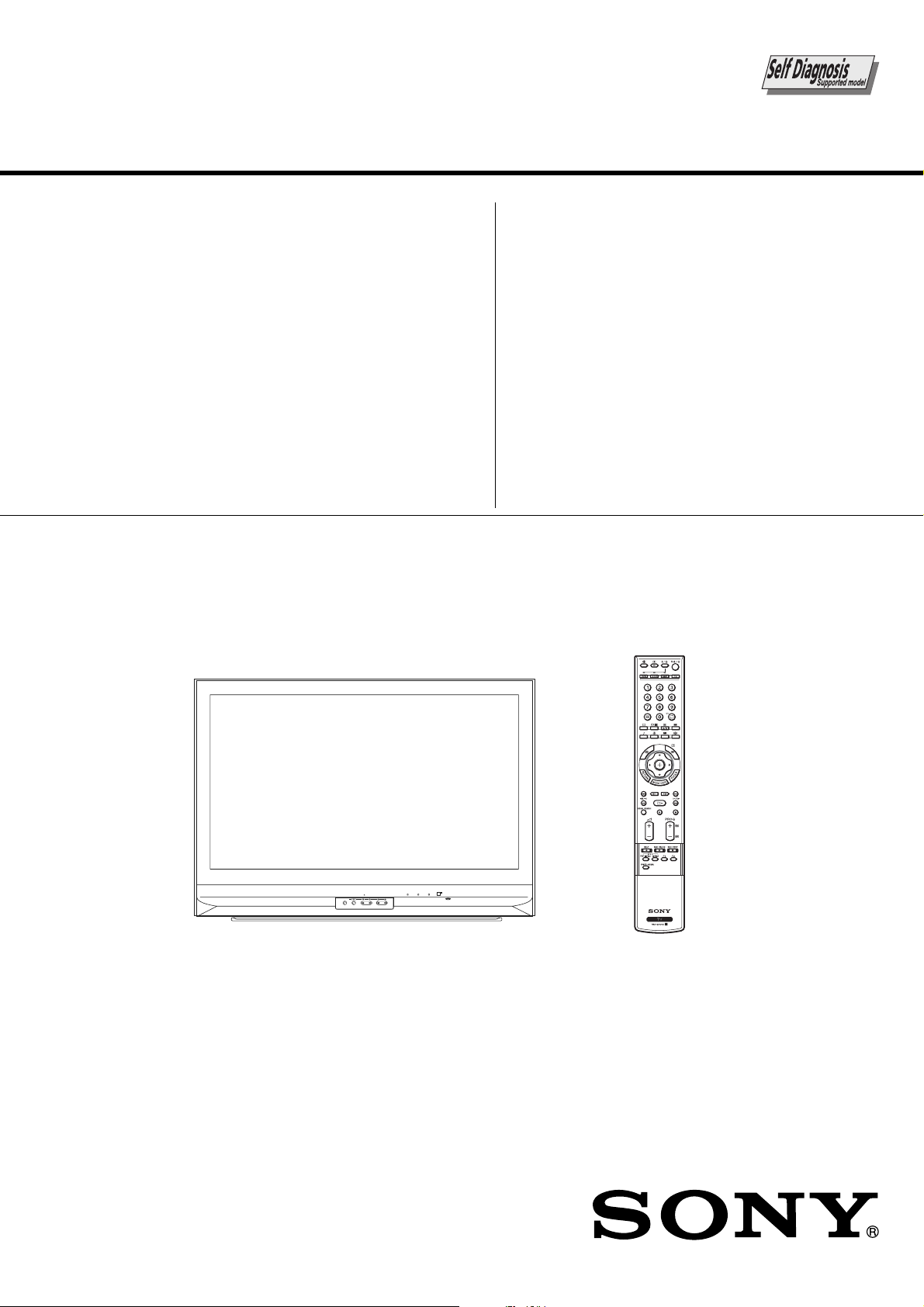
Model Name: KF-E42A10/E50A10
SERVICE MANUAL
Part No. : 9-872-770-01
Date SUPP./CORR. Description of SUP/COR
2005.10 – NEW –
Change of
main text
Page 2
SERVICE MANUAL
MIX5
CHASSIS
MODEL COMMANDER DEST. CHASSIS NO.
–––––– –––––––––––– ––––– –––––––––––
KF-E42A10
KF-E42A10
KF-E50A10
KF-E50A10
RM-GA004
RM-GA004
RM-GA004
RM-GA004
OCE
E
OCE
E
MODEL COMMANDER DEST. CHASSIS NO.
–––––– –––––––––––– ––––– –––––––––––
TIMER LAMP
PUSH OPEN
WEGA GATE
TV/VIDEO
CANNELVOLUME
KF-E42A10/E50A10
POWER/STANDBY
POWER
RM-GA004
LCD PROJECTION TV
Page 3
KF-E42A10/E50A10
RM-GA004 RM-GA004
Specifications
Display Unit
Power Requirement:
220-240 V AC, 50/60 Hz
Projection System
3 LCD (Liquid Crystal Display) Panels, 1 lens
projection system
LCD Panel
Size 0.73 inch TFT LCD panel
Resolution 1,280 pixels 720 lines
Projection Lenses
High performance, large-diameter highbrid lens F2.4
Lamp
UHP lamp, 100 W, XL-2400
Screen Size:
KF-E50A10: 50 inches (approx. 125.5 cm measured
diagonally)
KF-E42A10: 42 inches (approx. 105.2 cm measured
diagonally)
Display Resolution:
1,280 pixels (horizontal) ×
Power Consumption:
KF-E50A10: 195 W
KF-E42A10: 195 W
Standby Power Consumption:
KF-E50A10: 1 W or less
KF-E42A10: 1 W or less
Dimensions (w h d):
KF-E50A10:
Approx. 1,184 827 408 mm
KF-E42A10:
Approx. 999 72 2 357 mm
Weight:
KF-E50A10: Approx. 32 kg
KF-E42A10: Approx. 27 kg
×
×
×
××
TV System
I, D/K, B/G, M
Colour System
PAL, PAL60, SECAM, NTSC 4.43, NTSC 3.58
Antenna
75 ohm external terminal
Channel Coverage
B/G
VHF: E2 to E12 / UHF: E21 to E69 /
CATV: S01 to S03, S1 to S41
VHF: 0 to 12, 5A, 19A / UHF: 28 to 69 /
CATV: S01 to S03, S1 to S41(Australia only)
VHF: 1 to 11 / UHF: 21 to 69 /
CATV: S01 to S03, S1 to S41(New Zealand only)
I
UHF: B21 to B68 / CATV: S01 to S03, S1 to S41
D/K
VHF: C1 to C12, R1 to R12 / UHF: C13 to C57,
R21 to R60 /
CATV: S01 to S03, S1 to S41, Z1 to Z39
M
VHF: A2 to A13 / UHF: A14 to A79 /
CATV: A8 to A2, A to W+4, W+6 to W+84
720 lines (vertical)
×
Terminals
S VIDEO 1 (4-pin mini DIN):
Y: 1.0 Vp-p, 75 ohms unbalanced, sync negative
C: 0.286 Vp-p (Burst signal), 75 ohms
VIDEO/AUDIO IN 1/3:
VIDEO:
1 Vp-p, 75 ohms unbalanced, sync negative
AUDIO:
500 mVrms
Impedance: 47 kilohms
VIDEO/AUDIO IN 2:
Y, PB/CB, PR/CR (Component video) :
Y : 1.0 Vp-p, 75 ohms unbalanced, sync negative
R/CR : 0.7 Vp-p, 75 ohms
P
B/CB : 0.7 Vp-p, 75 ohms
P
Signal format : 480i, 576i, 480p, 576p, 720p,1080i
VIDEO:
1 Vp-p, 75 ohms unbalanced, sync negative
AUDIO:
500 mVrms
Impedance: 47 kilohms
HD/DVD IN 1/2: /
B/CB, PR/CR (Component video) :
Y, P
Y : 1.0 Vp-p, 75 ohms unbalanced, sync negative
P
R/CR : 0.7 Vp-p, 75 ohms
B/CB : 0.7 Vp-p, 75 ohms
P
Signal format : 480i, 576i, 480p, 576p, 720p,1080i
AUDIO:
500 mVrms
Impedance: 47 kilohms
VIDEO/AUDIO OUT:
VIDEO:
1 Vp-p, 75 ohms unbalanced, sync negative
AUDIO:
More than 1 Vrms at the maximum volume setting
AUDIO OUT:
More than 1 Vrms at the maximum volume setting
(Variable)
More than 500 mVrms (Fixed)
PC IN :
VIDEO: (RGB)
D-sub 15-pin, analogue RGB, 0.7 Vp-p, 75 ohms,
positive
AUDIO:
Stereo minijack, 0.5 Vrms, 1 kilohm
See the PC Input Signal Compatibility Chart on page 27.
HDMI IN:
HDMI
Video: 480i, 480p, 576i, 576p, 720p, 1080i
Audio: Two channel linear PCM 32, 44.1 and
48 kHz, 16, 20 and 24 bits
AUDIO:
500 mVrms (100% modulation)
Impedance: 47 kilohms
Headphones i
Stereo minijack
Impedance: 16 ohms
/
//
/
Sound Output
KF-E50A10: 12 W + 12 W
KF-E42A10: 12 W + 12 W
Design and specifications are subject to change
without notice.
– 2 –
Page 4
K RM-GA004 RM-GA004
21 93678
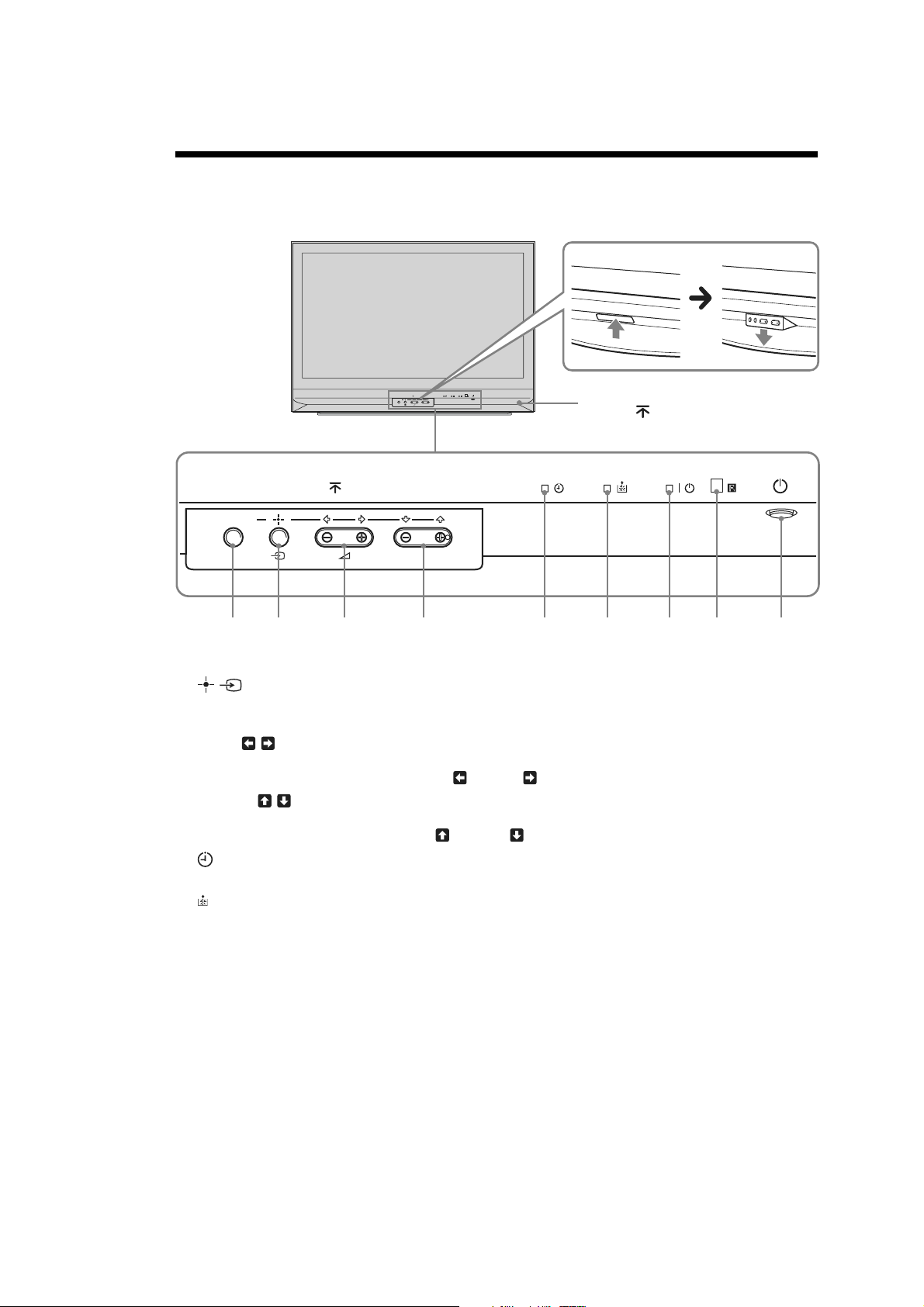
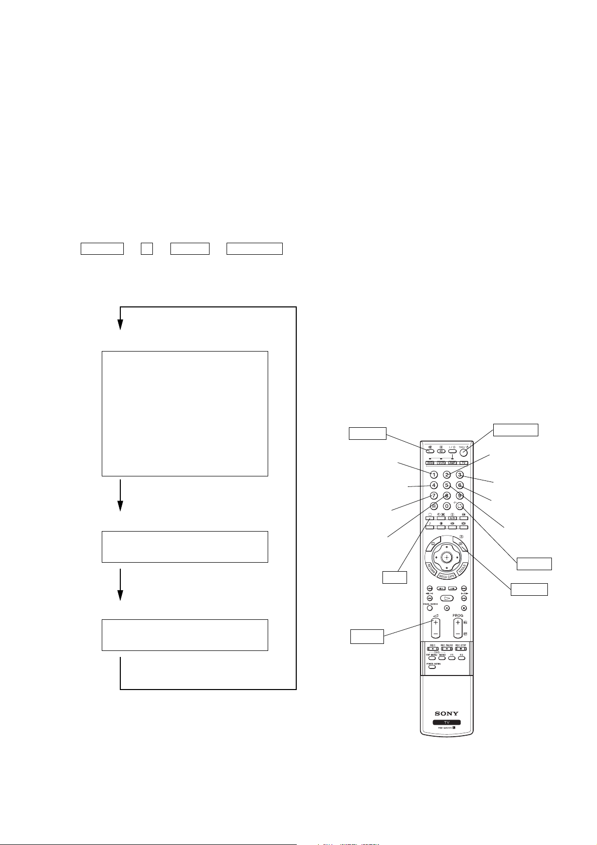
Overview of the TV buttons and indicators
To open the panel
To open the front panel of your TV,
WEGA GATE
PROG
push up the panel door just under
0
the mark.
KF-E42A10/E50A10
WEGA GATE
PROG
54
1 WEGA GATE
Displays WEGA GATE.
2
Confirms the selection or setting.
Selects the video equipment connected to the TV’s video inputs.
3 2 +/-/ /
Increases (+) or decreases (-) the volume.
In TV menu: Moves through the options left ( ) or right ( ).
4 PROG +/-/ /
In TV mode: Selects the next (+) or previous (-) channel.
In TV menu: Moves through the options up ( ) or down ( ).
5 indicator
Lights up in amber when the Sleep Timer/On Timer is set.
6 indicator
Flashes up in red when the lamp for the light source has burned out.
7 \ 1 indicator
Flashes in green when the light source is preparing to turn on. Lights up in green when the TV is switched on.
Lights up in red when the TV is in standby mode. When the lamp door or the lamp itself is not securely attached, the
red indicator will continue to flash in intervals of three blinks at a time.
8 Remote control sensor
Point the remote here.
9 1
Switches the TV on or off.
– 3 –
Page 5

KF-E42A10/E50A10
RM-GA004 RM-GA004
Projection Lamp
Your TV uses a projection lamp as its light source. As
with any lamp, it has lifespan and needs to be replaced
when the Lamp indicator flashes or the screen
becomes darker.
Notes
After turning on your TV, it may take a while (1 minute or
less) before the picture appears.
When the projection lamp wears out, the screen goes dark.
Replace the lamp with a new Sony XL-2400 replacement
lamp (not supplied). How to replace the lamp, see page 5.
Warning
The light emitted from the lamp is quite bright when your TV
is in use. To avoid eye discomfort or injury, do not look into
the light housing when the power is on.
– 4 –
Page 6
Replacing the lamp
The projection lamp, which illuminates the picture,
has a limited life.
If the screen becomes dark, the color looks unusual, or
the LAMP indicator on the front of the projection TV
flashes, it is time to replace the lamp with a new one
(not supplied).
WARNING
Electric appliances can cause fire or high temperature,
resulting in injury or death. Be sure to follow the instructions
below.
Use a Sony XL-2400 replacement lamp (not supplied) for
replacement. Use of any other lamp may damage the
projection TV.
Do not remove the lamp for any purpose other than
replacement. Doing so may cause injury or fire.
Do not put flammable materials and metal objects inside
the lamp receptacle of the TV after removing the lamp.
Doing so may cause fire or electrical shock. Do not touch
the lamp receptable once the lamp has been removed.
When the lamp eventually burns out, you may hear a
noticeable pop sound. This is normal and it is inherent to
this type of lamp.
In rare instances, the bulb may pop inside the lamp unit,
but the lamp unit is designed to contain all of the broken
glass pieces inside the lamp unit.
KF-E42A10/E50A10
K RM-GA004 RM-GA004
1
Turn off the power on the main unit. Wait
several minutes, then unplug the power
cord.
(The cooling fan will continue to blow for
about two minutes after turning the power
off.)
2
Wait at least 30 minutes after unplugging
the power cord to allow the lamp to cool
down before replacing it. To avoid being
burned, do not touch the lamp receptable
once the lamp has been removed.
3
Take the new lamp out of the box.
Do not touch the glass portion of the new
lamp.
Notes
Do not shake the lamp. Vibration can damage the
lamp or shorten its life.
Avoid touching the front glass of a new lamp or the
glass of the lamp receptacle. This may reduce picture
quality or lamp life.
4
Remove the outside lamp cover.
Disposing of the lamp
This product contains mercury. For disposal or
recycling information, please contact your local
authorities.
Do not leave the used lamp near flammable
materials or within the reach of children.
Do not pour water onto the used lamp or put any
object inside the lamp. Doing so may cause the
lamp to burst.
5
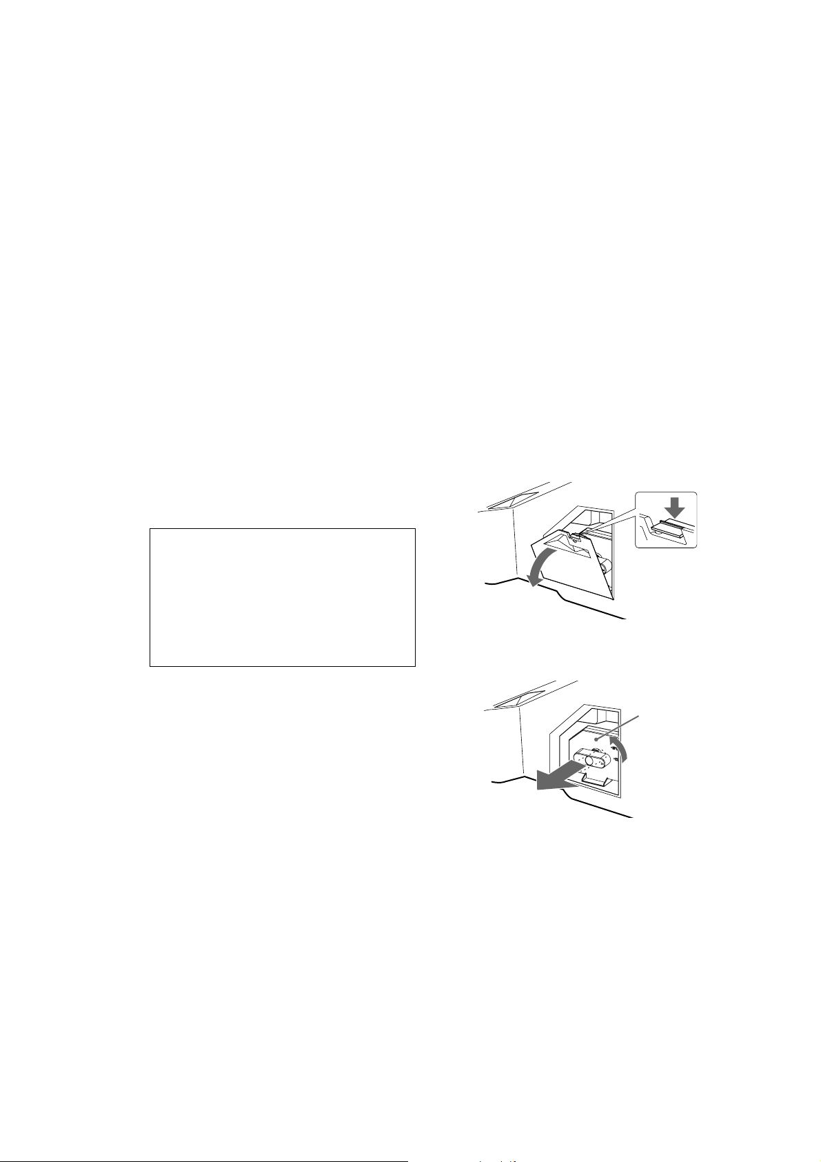
Remove the lamp door.
Turn the knob counterclockwise to OPEN and pull
out the cover.
Lamp door
– 5 –
Page 7
KF-E42A10/E50A10
RM-GA004 RM-GA004
6
Pull out the lamp.
Hook a finger through the loop of the lamp handle
and pull the handle upwards. Then pull the lamp
straight out.
Notes
The lamp is very hot immediately after use. Never
touch the glass portion of the lamp or the surrounding
parts.
After the used lamp has cooled, place it into the empty
box of the replacement lamp. Never put the used lamp
into a plastic bag.
7
Put the new lamp into its place.
Mount the new lamp securely. Failure to do so
may cause a fire or the screen to go dark.
9
Put the outside lamp cover back in its
place.
Notes
Consult your Sony dealer for a Sony XL-2400
replacement lamp.
Take great care when replacing the lamp or plugging
in/unplugging the connecting cords. Rough handling
may cause the TV to fall, damaging the TV, the TV
stand and the floor.
Note
If the lamp is not securely reattached, the self-diagnostic
function may be triggered and the POWER/STANDBY
indicator flashes three times.
8
Reattach the lamp door.
Turn the knob back to CLOSE and secure the
cover.
– 6 –
Page 8

CAUTION
These servicing instructions are for use by qualified service personnel only.
To reduce the risk of electric shock, do not perform any servicing
other than that contained in the operating instructions unless you
are qualified to do so.
WARNING!!
AN ISOLATION TRANSFORMER SHOULD BE USED DURING
ANY SERVICE TO AVOID POSSIBLE SHOCK HAZARD, BECAUSE OF LIVE CHASSIS.
THE CHASSIS OF THIS RECElVER IS DIRECTLY CONNECTED
TO THE AC POWER LINE.
SAFETY-RELATED COMPONENT WARNING!!
COMPONENTS IDENTIFIED BY SHADING AND MARK ! ON THE
SCHEMATIC DIAGRAMS, EXPLODED VIEWS AND IN THE
PAR TS LIST ARE CRITICAL TO SAFE OPERATION. REPLACE
THESE COMPONENTS WITH SONY PARTS WHOSE PART NUMBERS APPEAR AS SHOWN IN THIS MANUAL OR IN SUPPLEMENTS PUBLISHED BY SONY. CIRCUIT ADJUSTMENTS THAT
ARE CRITICAL TO SAFE OPERATION ARE IDENTIFIED IN THIS
MANUAL. FOLLOW THESE PROCEDURES WHENEVER CRITICAL COMPONENTS ARE REPLACED OR IMPROPER OPERATION IS SUSPECTED.
KF-E42A10/E50A10
K RM-GA004 RM-GA004
– 7 –
Page 9

KF-E42A10/E50A10
RM-GA004 RM-GA004
TABLE OF CONTENTS
Section Title Page
–––––– –––– ––––
1. SELF DIAGNOSIS FUNCTION ..................... 10
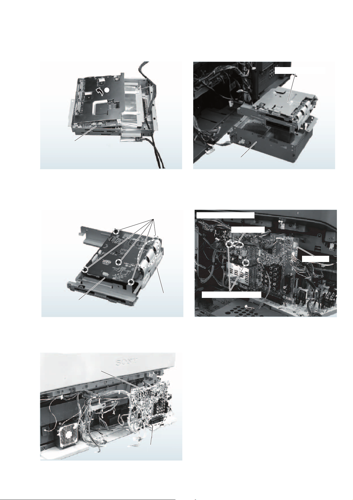
2. DISASSEMBLY
2-1. Rear Cover .......................................................... 15
2-2. Service Position .................................................. 16
2-3. Terminal Bracket ................................................ 17
2-4. HPC Board .......................................................... 17
2-5. AS Board ............................................................ 17
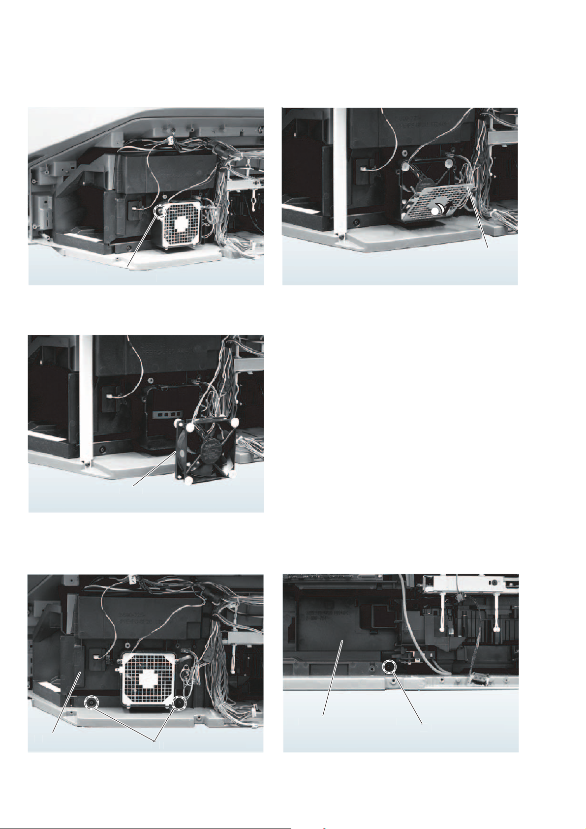
2-6. D.C Fan (Under The AS Board) ........................ 18
2-7. B Block ............................................................... 18
2-8. B Board ............................................................... 18
2-9. B and QG Boards ............................................... 19
2-10. QG Board ............................................................ 19
2-11. P Board ............................................................... 19
2-12. AGU Board ......................................................... 19
2-13. DC Fan ................................................................ 20
2-14. Main Duct (R) .................................................... 20
2-15. Duch Block Assembly
(Without Main Duct (R)) ................................... 20
2-16. D.C. Fan (Sirocco) ............................................. 21
2-17. Speaker Grill Block Assembly ........................... 21
2-18. HA and HB Boards ............................................ 21
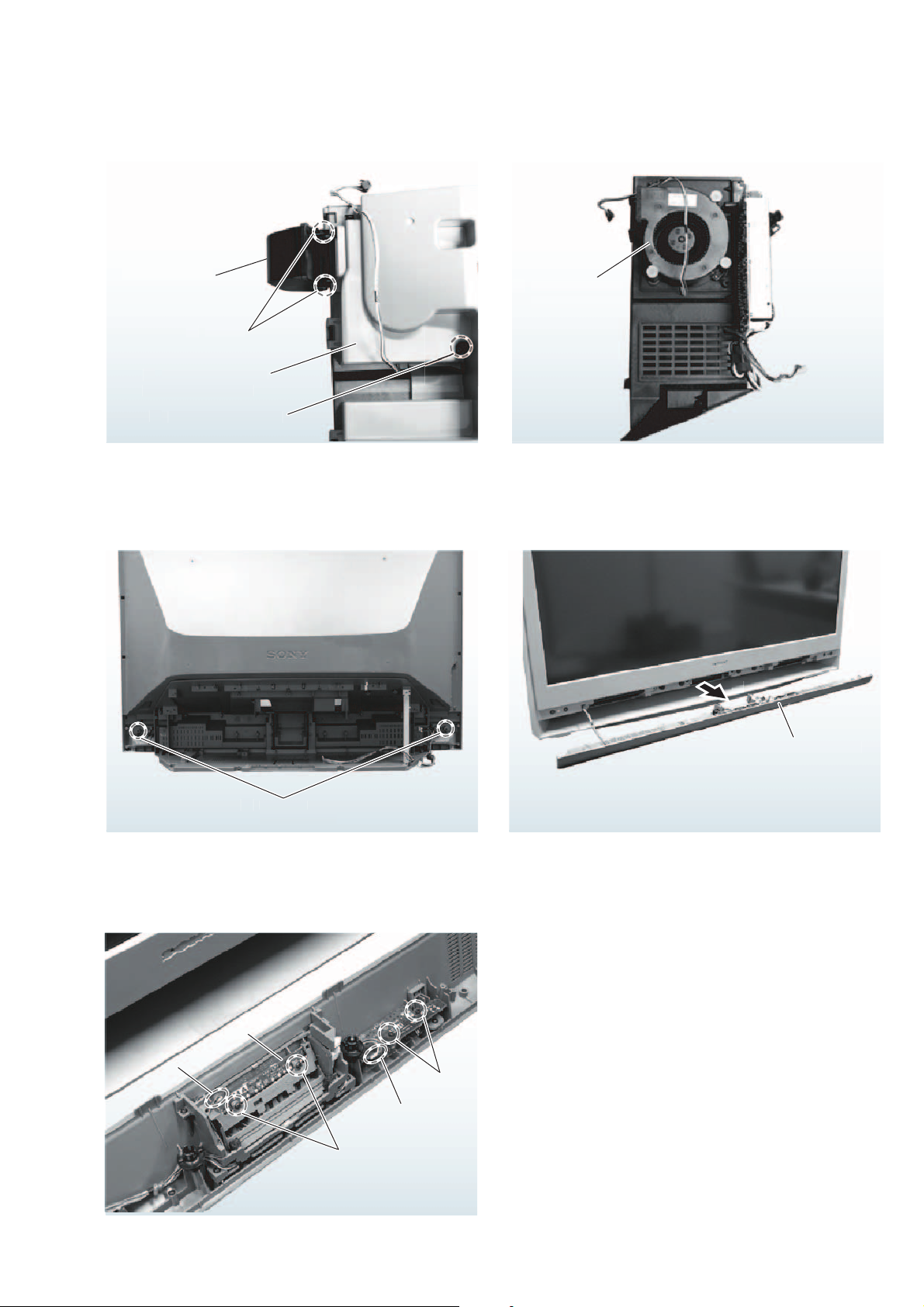
2-19. Screen Frame Block Assembly .......................... 22
2-20. Speakers .............................................................. 22
2-21. Rear Cover (With Mirror) .................................. 22
2-22. How to Replace Optics Unit .............................. 23
2-22-1. Remove Lamp Bloxk (1) ............................ 23
2-22-2. Remove Lamp Bloxk (2) ............................ 23
2-22-3. Remove Lamp Bloxk (3) ............................ 23
2-22-4. Remove Cover, Rear (1) ............................. 23
2-22-5. Remove Cover, Rear (1-2) .......................... 23
2-22-6. Remove Cover, Rear (2) ............................. 23
2-22-7. Remove Stay (L), Side ................................ 24
2-22-8. Pull Out Some Blocks (1) ........................... 24
2-22-9. Pull Out Some Blocks (2) ........................... 24
2-22-10. Pull Out Some Blocks (3) ........................... 24
2-22-11. Pull Out Some Blocks (4) ........................... 25
2-22-12. Pull Out Some Blocks (5) ........................... 25
2-22-13. Pull Out Some Blocks (6) ........................... 25
Section Title Page
–––––– –––– ––––
2-22-14. Pull Out Some Blocks (7) ........................... 26
2-22-15. Pull Out Some Blocks (8) ........................... 26
2-22-16. Pull Out Some Blocks (9) ........................... 26
2-24-18. Remove Optics Unit .................................... 26
3. ELECTRICAL ADJUSTMENTS
3-1. Electrical Adjustment by Remote Commander .... 27
3-1-1. Method of Setting the Service Adjustment
Mode ............................................................... 27
3-1-2. Service Mode Adjustment ............................ 27
3-1-3. Memory Write Confirmation Method .......... 27
3-1-4. Adjusting Buttons and Indicator ................... 27
3-2. To read Lamp and Panel time ............................ 28
3-3. Test Reset ........................................................... 28
4. DIAGRAMS
4-1. Block Diagram (1) .............................................. 29
Block Diagram (2) .............................................. 30
Block Diagram (3) .............................................. 31
Block Diagram (4) .............................................. 32
Block Diagram (5) .............................................. 33
4-2. Frame Schematic Diagram ................................. 34
4-3. Circuit Boards Location ..................................... 35
4-4. Schematic Diagrams ........................................... 35
(1) Schematic Diagram of AS (1/2) Board .............. 36
(2) Schematic Diagram of AS (2/2) Board .............. 37
(3) Schematic Diagram of GT (1/2) Board ............ 38
(4) Schematic Diagram of GT (2/2) Board ............ 39
(5) Schematic Diagram of HA Board ..................... 40
(6) Schematic Diagram of HB Board ...................... 41
(7) Schematic Diagram of HC Board ..................... 42
(8) Schematic Diagram of S2 Board ...................... 43
(9) Schematic Diagram of T1, T2 Boards .............. 44
4-5. Printed Wiring Boards ........................................ 45
(1) AS Board ............................................................ 45
(2) GT Boards .......................................................... 46
(3) HA, HB Boards .................................................. 47
(4) HC, S2, T1, T2 Boards ....................................... 48
4-6. Semiconductors .................................................. 49
– 8 –
Page 10

Section Title Page
–––––– –––– ––––
5. EXPLODED VIEWS
5-1. Screen Mirror Block, Cover ............................... 50
5-2. B Block, Chassis Assembly ............................... 51
5-3. Lamp Duct Assembly, Optics Unit Block ......... 52
6. ELECTRICAL PARTS LIST
• AS Board ................................................................... 53
• GT Board .................................................................. 56
• HA Board .................................................................. 58
• HB Board .................................................................. 59
• HC Board .................................................................. 59
• S2 Board .................................................................... 60
• T1 Board ................................................................... 60
• T2 Board ................................................................... 60
KF-E42A10/E50A10
K RM-GA004 RM-GA004
– 9 –
Page 11
KF-E42A10/E50A10
RM-GA004 RM-GA004
1. Summary of Self-Diagnosis Function
-This device includes a self-diagnosis function.
-Incaseofabnormalities, the POWER/STANDBY indicator automatically blinks. It is
possible to predict the abnormality location by the number of blinks. The Instruction
Manual describes blinking of the POWER/STANDBY indicator.
-Ifthe symptom is not reproduced sometimes in case of a malfunction, there is recording of
whether a malfunction was generated or not. Operate the remote command to confirm the
matter on the screen and to predict the location of the abnormality.
2. Diagnosis Items and Prediction of Malfunction Location
-When a malfunction occurs the POWER/STANDBY indicator only blinks for one of the
following diagnosis items. In case of two or more malfunctions, the item which first
occurred blinks. If the malfunctions occurred simultaneously, the item with the lower
blink count blinks first.
-The screen display displays the results regarding all the diagnosis items listed below.
Thedisplay "0" means that no malfunctions occurred.
SECTION 1
SELF DIAGNOSIS FUNCTION
Number of times
Diagnosis Item
Lamp temp. over
La
mp cover error 3
Fanstopped 4 times
Lamp driver error 5 times
Low B error 6 times
Lamp error LAMP-LED flashes - No picture/No sound
POWER/STANDBY
indicator blinks
2 times
times
Probable Cause
Location
-Lampcover is not
attached securely.
-Fan1,Fan2, F an 3,
4 or Fan 5
supplied.
-Fan connector is not
attached securely.
-Lampdriver is faulty. - No picture/No sound
- B_12V is not
supplied.
-Lampfor the light
source burns out.
power is not
Fan
Defected symptoms
-Nopicture/No sound
-Nopicture/No sound
-Nopicture/No sound
– 10 –
Page 12
K RM-GA004 RM-GA004
3. Blinking count display ofPOWER/STANDBY indicator
-One blink is not used for self-diagnosis.
-Example
Diagnosis item
LEDblinks
KF-E42A10/E50A10
Lamp cover 3 times
Fan 4 times
LEDON:0.3sec
LEDOFF : 0.3sec
LED OFF
LAMP
STANDBY
STD / DUO
TIMER
POWER/STANDBY
POWER
POWER
STD/DUO
3.0sec
-Release of POWER/STANDBY indicator blinking
The POWER/STANDBY indicatorblinking display is released by removing the plug from
the power or leaving for 2 minutes.
4. Self-diagnosis screen displays
-Incases of malfunctions where it is not possible to determine the symptom such as when
the power goes off occasionally or when the screen disappears occasionally, there is a
screen display on whether the malfunction occurred or not in the past (and whether the
detection circuit operated or not) in order to allow confirmation.
<Screen Display Method>
-Quickly press the remote command button in the following order from the standby state.
DISPLAY 5 - POWER
ChannelVol
Be aware that thisdiffers from
the method of entering the
service mode (Vol +).
SELF CHECK
1:LAMP_ERROR 0
2 : LAMP_TEMP 0
2 : TEMP_ERROR 0 No use
3:LAMP_COVER 0
4 : FAN_ERROR 0
5:LAMP_DRIVER 0
6:LOWB_ERROR 0
7:AUDIO_PROT 0 No use
8:D_OVP 0 No use
10 : ATSC_OVP 0 No use
-Numeral "1" means a fault was detected one time
-Numeral "0" means that no fault was detected
– 11 –
Page 13

KF-E42A10/E50A10
RM-GA004 RM-GA004
-The results display is not automatically cleared. In case of repairs and after repairs, check
the self-diagnosis screen and be sure to return the results display to "0".
-Ifthe results display is not returned to "0" it will not be possible to judge a new malfunction
after completing repairs.
<Method of Clearing Results Display>
1. Power off (Set to the standby mode)
2. Channel Vol
DISPLAY 5 - POWER
3. Channel
8ENTER
<Method of Ending Self-Diagnosis Screen>
-When ending the self-diagnosis screen completely, turn the power switch OFF on the
remote commander or the main unit.
5. Self-Diagnosis function operation
1:Lamp_ERROR When the lamp is broken.
2:lamp temp over When the inside temperature sensed with IC7021, IC7180 and IC603 mounted
on HB board, S2 board and C board respectively exceed the threshold, the lamp
turns off.
3:lamp cover When the lamp cover is opened the connector of the lamp is not fixed, the lamp
turns off.
4:FAN When any FAN (FAN1~FAN4) is stopping or harness is not connected correctly,
the lamp turns off.
5:Lamp Driver When the ballast is not working with high voltage, the lamp turns off.
6:Low B error When the voltage B_12V is low, TVM(TV u-com) detects it and makes turn off
the lamp.
– 12 –
Page 14
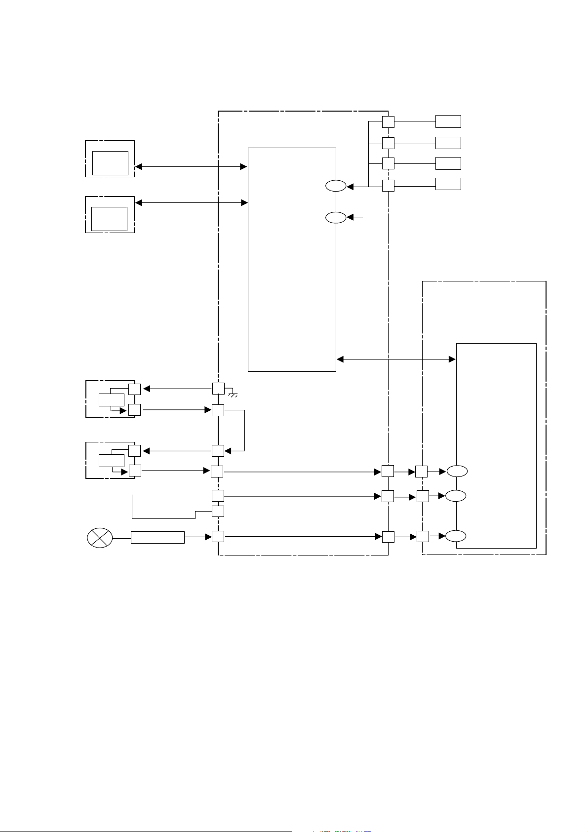
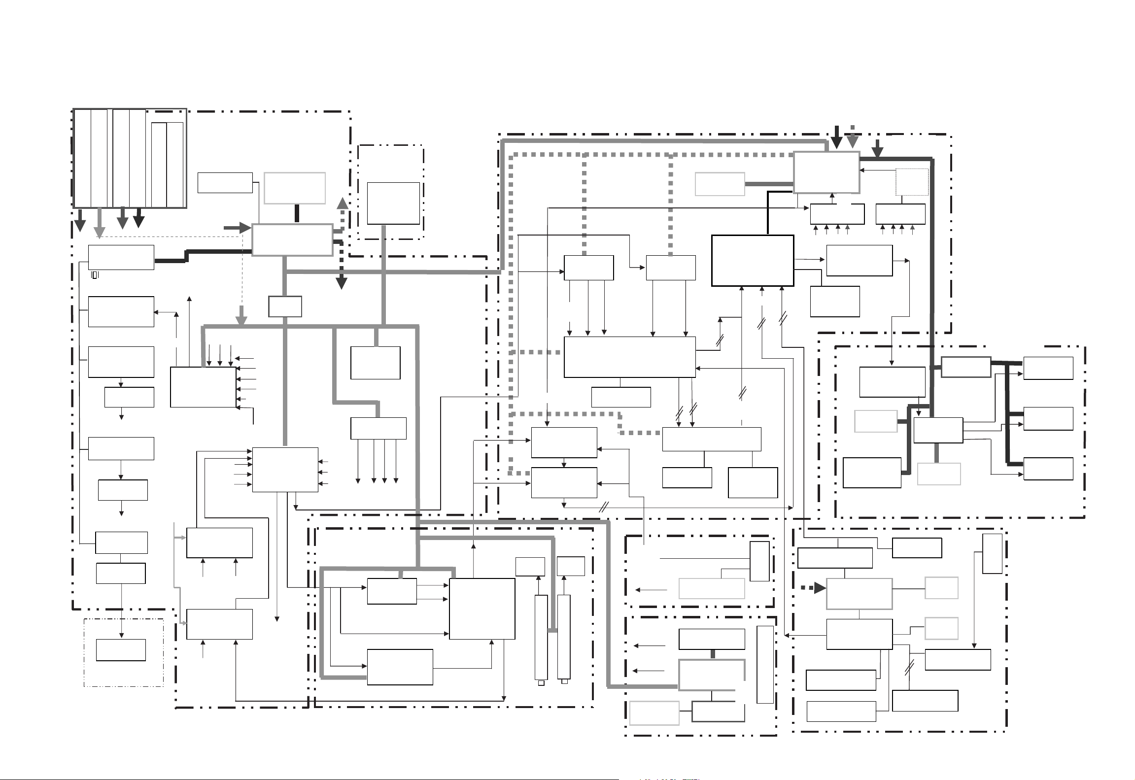
BLOCK DIAGRAM
KF-E42A10/E50A10
K RM-GA004 RM-GA004
AGU board
S2 board
IC7180
Temp.
Sensor
HB board
IC7021
Temp.
Sensor
T2 board
SW
IC8002
TV Micro-computer
IIC-TV
FAN-ERR
IIC-TV
LB-ERR
CN8403
3
1
2
1
38
128
IIC
4
7
10
13
CN8002
+12V
Fan1
Fan2
Fan3
Fan4
B board
IC4100
BE Micro-computer
IIC
T1 board
SW
Lamp
1
3
HV-DET
Lamp Driver
CN8410
CN8410
CN8410
14
15
13
12
CN8003
8
5
CN8003
CN8003
7
7
8
5
7
133
LAMP COVER
134
LAMP-HV-DET
132
LAMP-PROT
– 13 –
Page 15

KF-E42A10/E50A10
RM-GA004 RM-GA004
Reading Lamp and Panel time
Use the following to determine the lamp and panel time of a set.
Screen Display Method
In standby mode, press the buttons on the Remote Commander sequentially, in rapid succession, as shown below:
1. Press Display , Channel 5 , Sound Volume + , Power ON
2. To enter BE-micro service menu, press JUMP 2 times.
3. To display the lamp time, press Channel-4.
The screen displays:
“ Total lamp time is 14 hours”
4. To display the panel time, press Channel-4.
The screen displays:
“ Total panel time is 14 hours”
5. To display the lamp time clear, press Channel-5
7 times and Channel-1.
To reset the lamp time press Channel-3 > MUTING > ENT.
WRITE (Character color is red) is momentarily displayed and the lamp time is reset to “0”.
Exiting Service Mode
To exit the service mode, please turn off the set using the Remote Commander or the power switch.
CONFIGRATION 00 SERVICE
CP18_COLOR_SYS 00 00A0 BE Micro
Press Channel-4
m
GW_SPECIAL 34 SERVICE
LAMP_TIME 02 00000014 BE Micro
Press Channel-4
m
GW_SPECIAL 34 SERVICE
PANEL_TIME 01 00000014 BE Micro
Press Channel-5 7 times,
m
Channel-1
OPTION_E 20 SERVICE
LAMP 01 0000 BE Micro
– 14 –
Page 16
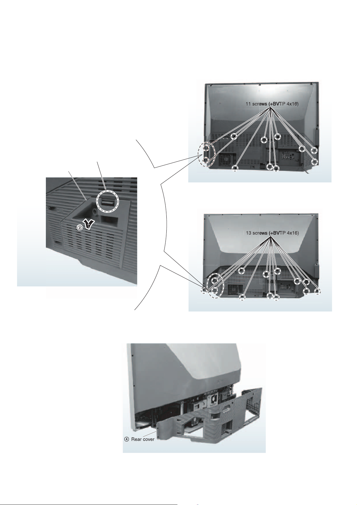
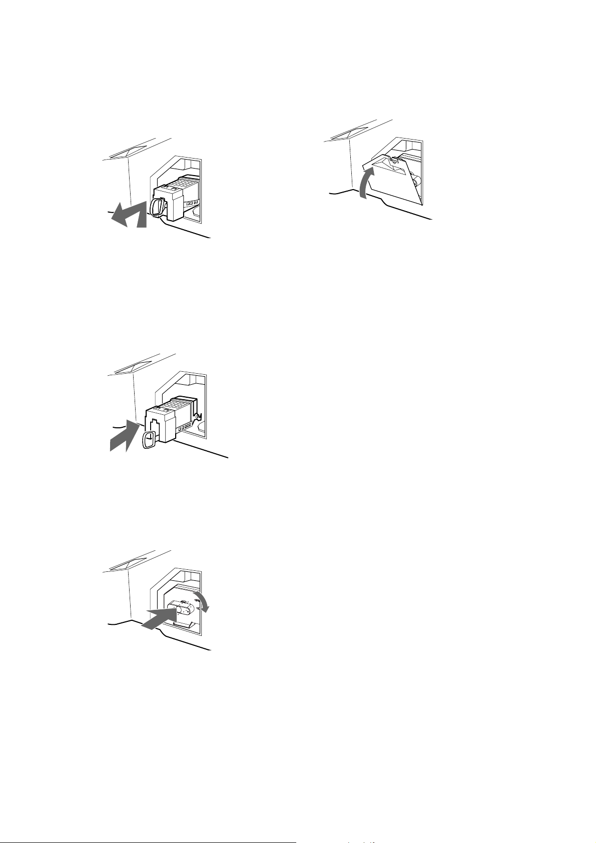
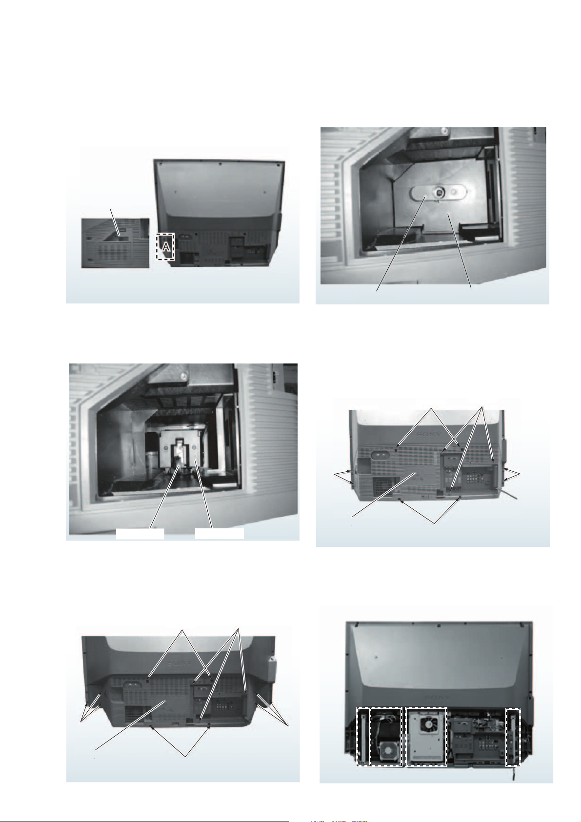
2-1. REAR COVER
3
3
1 Pull down the claw
Lamp door
SECTION 2
DISASSEMBLY
E42A10
KF-E42A10/E50A10
K RM-GA004 RM-GA004
E50A10
– 15 –
Page 17
KF-E42A10/E50A10
C
7
Loose
holders
RM-GA004 RM-GA004
2-2. SERVICE POSITION
A
3 Side stay (L)
C
B
1 2 screws (+BVTP 4x16)
B
4 4 screws (+BVTP 4x16)
A
5 Pull out B block slightly
6 Pull out chassis block slightly
n wire
– 16 –
Page 18
KF-E42A10/E50A10
3
2
2 screws
)
Terminal bracket
1
2 connectors
baord
K RM-GA004 RM-GA004
9 Tu rn chassis dssembly
8 Loosen wire holders
GT board B side
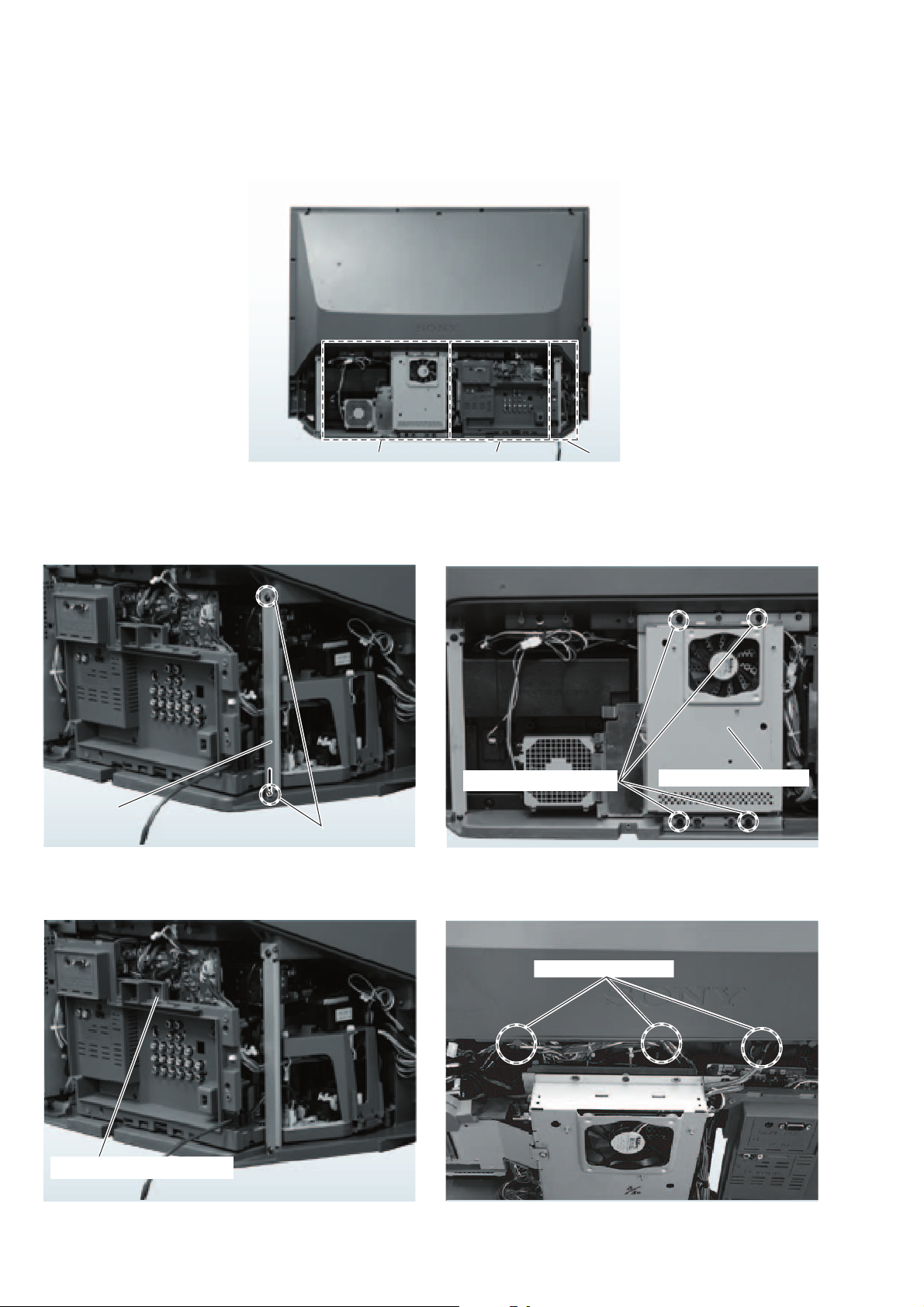
2-3. TERMINAL BRACKET 2-4. HPC BOARD
1 4 screws (+BVTP 3x12)
HPC
3
2 Screw (+PSW M3x5)
Te r mi nal brdcket
(+PVTP 4x16
2-5. AS BOARD
1 4 connectors
2 2 screws (+PSW M3x8)
2 2 screws (+PSW M3x8)
– 17 –
Page 19
KF-E42A10/E50A10
RM-GA004 RM-GA004
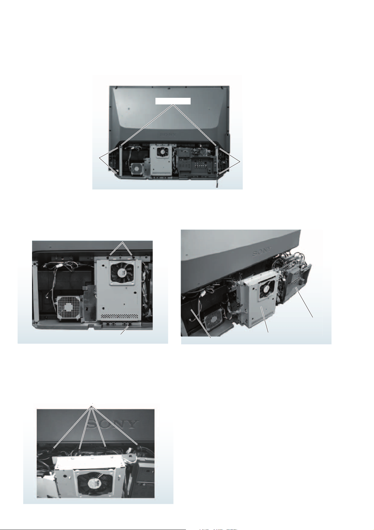
2-6. D.C FAN (UNDER THE AS BOARD)
1 2 screws (+BVTP 3x12)
2 F shield sheet (Fan)
3 D.C fan
2-7. B BLOCK
B block
2 3 connectors
2-8. B BOARD
1 Connector
B block
3 4 connectors
3 4 screws (+PSW M3x8)
1 QU bracket
2 3 connector
– 18 –
Page 20
B board
board
2
Connecto
1
Upp
lid of shield
3
)
1
Connecto
2
board
KF-E42A10/E50A10
K RM-GA004 RM-GA004
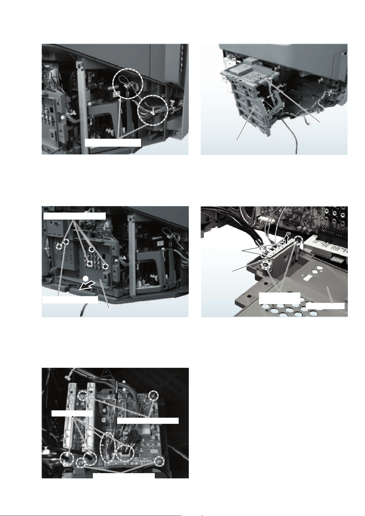
2-9. B AND QG BOARDS
B and QG boards
4
Shield case (DIGITAL)
2-10. QG BOARD 2-11. P BOARD
3 QG board
2 5 screws
(+PSW M3x8)
1 3 connectors
er
2 screws (+PSW M3x8
2-12. AGU BOARD
case
r
AGU
AUG
r
– 19 –
Page 21
KF-E42A10/E50A10
22
1
Screw
(
)
2
bly
)
)
)
RM-GA004 RM-GA004
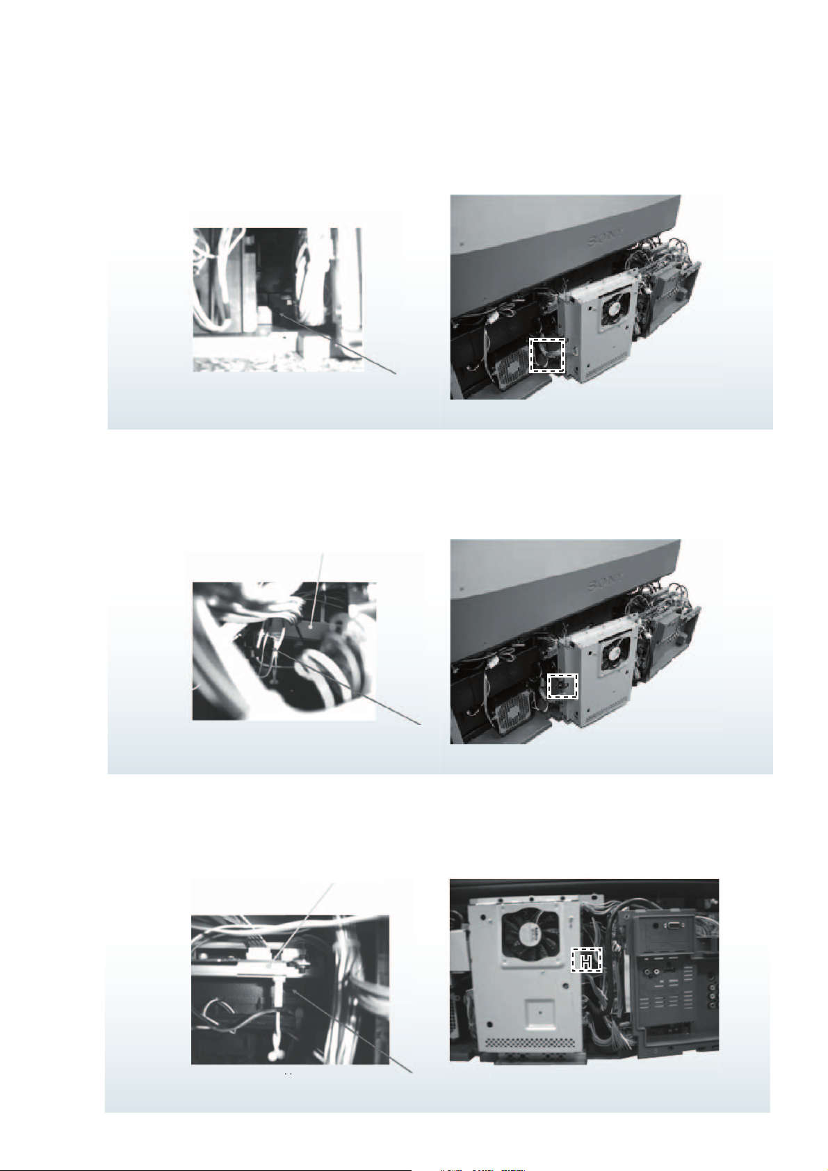
2-13. DC FAN
+BVTP 4x16
80 fan plate
DC fan
2-14. MAIN DUCT (R)
Pull out main duct (R
2 screws (+BVTP 4x16
2-15. DUCT BLOCK ASSEMBLY
(WITHOUT MAIN DUCT (R))
ull out duct block assem
crew (+BVTP 4x16
– 20 –
Page 22
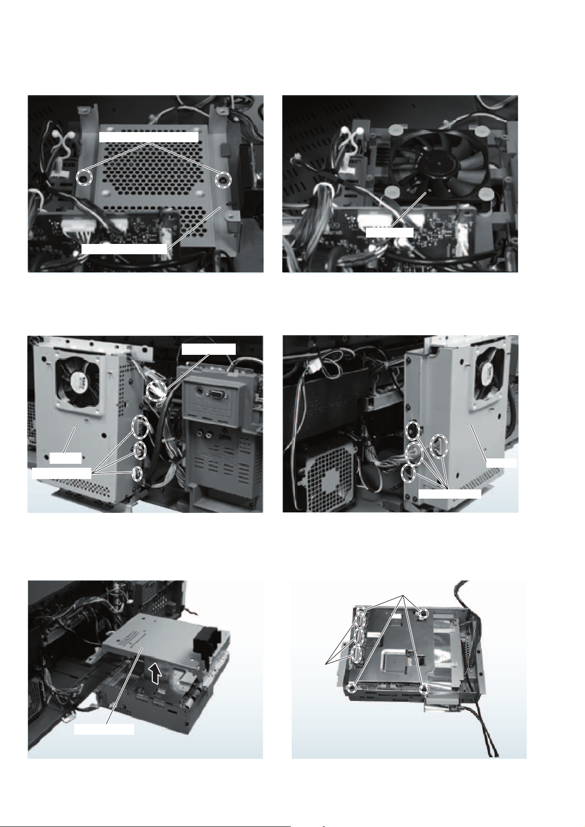
2-16. D.C. FAN (SIROCCO)
claws
OCCO
d
)
y
s
)
KF-E42A10/E50A10
K RM-GA004 RM-GA004
amp duct cover
2
Remove SIR
fan cover upwar
crew (+BVTP 4x16
2-17. SPEAKER GRILL BLOCK ASSEMBLY
Remove D.C. fan
sirrocco) upward
screw
+BVTP 4x16
2-18. HA AND HB BOARDS
3 HA board
1 Connector
5 2 Screws
4 Connector
2 2 screws
(+BVTP 3x12)
peaker grill block assembl
– 21 –
Page 23
KF-E42A10/E50A10
s
)
e
bly
s
)
s
)
6
y
s
)
)
RM-GA004 RM-GA004
2-19. SCREEN FRAME BLOCK ASSEMBLY
1 10 screws
(+BVTP 4x16) (E42A10)
13 screws
(+BVTP 4x16) (E50A10)
screw
+BVTP 4x16
block assem
2-20. SPEAKERS 2-21. REAR COVER (WITH MIRROR)
Rear cover (with mirror
screw
+PWTP2 4x16
creen frame block assembl
eaker
eaker
screw
+PWTP2 4x1
screw
+BVTP 4x16
reen fram
– 22 –
Page 24
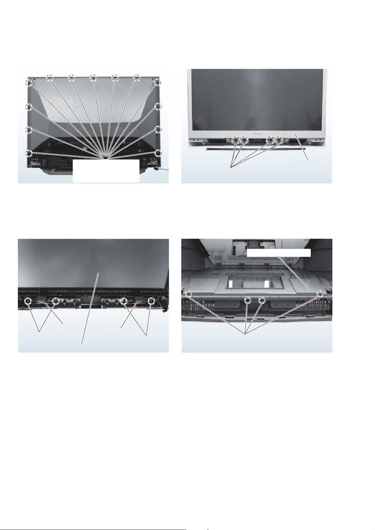
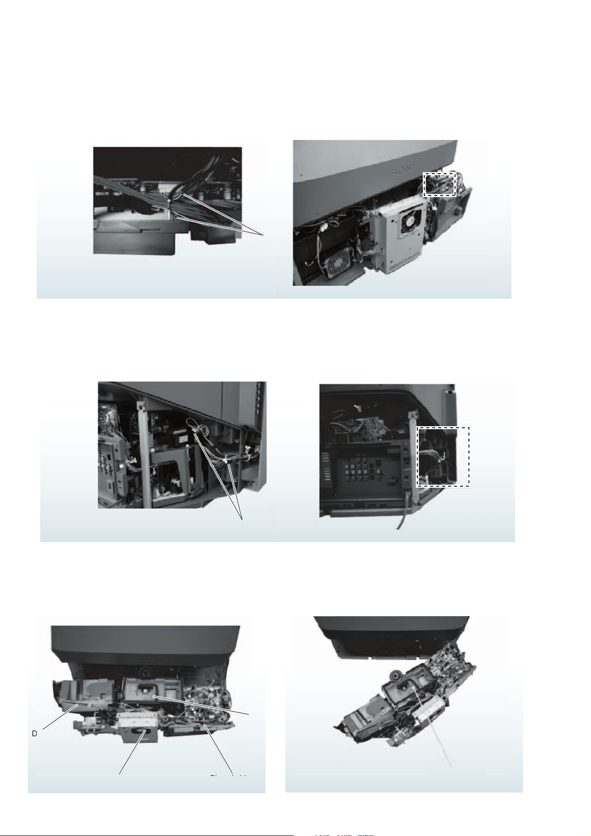
2-22. HOW TO REPLACE OPTICS UNIT
p
k
p
k
p
s
s
s
screws
ew
KF-E42A10/E50A10
K RM-GA004 RM-GA004
2-22-1. Remove Lamp Block (1)
Remove '' Door, Lamp ".
oor, Lam
2-22-3. Remove Lamp Block (3)
Pull the "Lever, Lock" below to remove "Lamp block".
2-22-2. Remove Lamp Block (2)
Turn left "Lever, Lock" below, and then remove "Door, Lamp".
ever, Loc
oor, Lam
2-22-4. Remove Cover, Rear (1)
Take off 11 screws (42"), and then pull out "Cover, Rear".
2 screws
over, Rear
ever, Loc
2-22-5. Remove Cover, Rear (1-2)
oor, Lam
2-22-6. Remove Cover, Rear (2)
Take off 13 screws (50"). It is removed "Cover, Rear".
3 screws
screw
2 screws
screw
2 screws
screw
over, Rear
2 screws
scr
E
E
B
B
D
D
C
C
– 23 –
Page 25
KF-E42A10/E50A10
,
RM-GA004 RM-GA004
2-22-7. Remove Stay (L), Side
Take off 4 screws, and then remove 2 "Stay (L), Side".
Stay (L), Side
2 screws
2-22-8. Pull Out Some Blocks (1)
Take off 4 screws.
< D >
< B >
2 screws
Screw
2 screws
< C >
2-22-9. Pull Out Some Blocks (2)
Pull out "B block", "Chassis block", and "Duct (R), Main"
a little bit.
Chassis block
B block
Duct (R), Main
2-22-10. Pull Out Some Blocks (3)
Unlock "Holder, Wire" as shown below.
older, Wire
– 24 –
Page 26
2-22-11. Pull Out Some Blocks (4)
unit block
i
Take off 1 screw.
< F >
KF-E42A10/E50A10
K RM-GA004 RM-GA004
3 screws
FF
1 screw
2-22-12. Pull Out Some Blocks (5)
Loose 1 special screw. (This screw can not be taken off.)
Optics unit block
< G >
2-22-13. Pull Out Some Blocks (6)
Take off 1 screw.
1 special screw
GG
c
1 speal screw
– 25 –
Page 27
KF-E42A10/E50A10
unit block
k
u
block
RM-GA004 RM-GA004
2-22-14. Pull Out Some Blocks (7)
Remove 2 connecters to pull out some blocks as shown below.
< I >
II
Connector
2-22-15. Pull Out Some Blocks (8)
Unlock "Purse Lock" to pull out some blocks as shown below.
< J >
Purse lock
2-22-16. Pull Out Some Blocks (9)
Pull out "B block", "Chassis block", "Duct block", and "Optics
Unit block".
JJ
2-22-17. Remove Optics Unit
Remove all connecters to remove "Optics Unit block" and then it.
nit bloc
ics
B block
– 26 –
Page 28
SECTION 3
ELECTRICAL ADJUSTMENTS
3-1. ELECTRICAL ADJUSTMENT BY REMOTE
COMMANDER
By using remote commander (RM-GA004), all circuit adjust-
ments can be made.
NOTE : Test Equipment Required.
1. Pattern Generator (with component outputs)
2. Oscilloscope
3. Digital multimeter
3-1-1. Method of Setting the Service Adjustment
Mode
KF-E42A10/E50A10
K RM-GA004 RM-GA004
3-1-2. Service Mode Adjustment
1. The SCREEN displays the item being adjusted.
2. Press “1” or “4” on the remote commander to select the
adjustment item.
3. Press “3” or “6” on the remote commander to change the data.
4. Press “2” or “5” on the remote commander to select the category.
Every time you press “2” (Category up).
5. If you want to recover the latest values press “-” then
“[ENTER]” to read the memory.
6. Press “[MUTING]” then “[ENTER]” to write into memory.
7. Turn power off.
1. Standby mode. (Power off)
2. DISPLAY t 5 t VOL (+) t TV POWER
on the remote commander.
(Press each button within a second.)
The following service screen will appear.
<TV micro>
STATUS 0 SERVICE
SHUTDOWN_LOG1 0 TV MICRO
ATI : H05-01.xx
SAIPH PROGRAM : 1.xxx
BOOT : x.xxx
NVM : 1.xxx
CHIMERA PROGRAM : 1.xxx
PACK : 1.xxx
OSD : x.xxx
NVM A0 : x.xxx
NVM AC : x.xxx
NVM AE : ----
HDMI : 1.xxx
Press “JUMP” key.
<Digiotal Module micro>
QM 0 0 SERVICE
INFO DTV
Press “JUMP” key.
<Method of setting the shipping condition>
1. Service Adjustment mode.
2. Press “8” then “[ENTER]”
3. Wait until appearing “ Initial Setup” display.
4. Disconnect AC plug and connect again to change factory re-
set condition completely.
3-1-3. Memory Write Confirmation Method
1. After adjustment, turn power off with the remote commander.
2. Turn power on and set to service mode.
3. Call the adjusted items again and confirm they were adjusted.
3-1-4. Adjusting Buttons and Indicator
MUTING
Adjustment item
up
Adjustment item
down
Initialize data
(Not stored)
User control goes
to the standerd state
(Shipping Conditions)
JUMP
TV POWER
Adjustment category
up
Data up
Data down
Adjustment category
down
ENTER
DISPLAY
<BE micro>
CONFIGRATION 00 0 SERVICE
CP18_COLOR_SYS
Press “JUMP” key.
00 00A0 BE Micro
VOL +
RM-GA004
– 27 –
Page 29
KF-E42A10/E50A10
RM-GA004 RM-GA004
FUNCTION OF KEYS ON COMMANDER
• 1 : Changes adjustment item. (item No. moves up)
• 4 : Changes adjustment item. (item No. moves down)
• 2 : Changes adjustment category.
(category moves up)
• 5 : Changes adjustment category.
(category moves down)
• 3 : Changes data value. (up)
• 6 : Changes data value. (down)
Commander Function
Button Mode Description
[MUTING] + [ENTER] WRITE Writes data to NVM.
- + [ENTER] READ Reads data from NVM.
8 + [ENTER] RESET Set the shipping condition.
3-2. H/V Center Confirmation and Adjustment
Please check the picture horizontal/vertical center after the replace-
ment of the following parts .
• Optical block
• Top assembly
1, Check H/V center with 480i monoscope signal in “Full “ mode .
2, If the center is shifted , adjust it with the following service items .
3-3. IRIS Adjustment
Please check it after the replacement of the following parts.
• IRIS unit+Optics unit block+C board
• B board
Check values of the service data in NVM on C board
#0 BL_U_TOP
#1 BL_U_BOTTOM
DBL_CTRL_AC
and write the same values on C board to the service data in NVM
on B board.
DBL_CTRL
#2 BL_MAX
#3 BL_MIN
#4 IRIS_GAIN
#5 HALL_GAIN
#0 BL_U_TOP
#1 BL_U_BOTTOM
#2 BL_MAX
#3 BL_MIN
#4 IRIS_GAIN
#5 HALL_GAIN
ODHS (for H center)
ODVS (for V center)
ODHS
ODVS
– 28 –
Page 30
SECTION 4
K RM-GA004 RM-GA004
DIAGRAMS
4-1. BLOCK DIAGRAM (1)
GA GW T ROY Block Diagram
JIG Connector
CN8008
S2
LM75BIM- 5L
5,6 SDA/SCL_TV
11,12SDA/SCL_E
RESE
3 E- B INT(MD)
15,16 TXD/ RXD _TV
17,18 TXD/ RXD JIG_API
4 JIG - E_BINT
T
BD4729GTRM 24128- BWMNT empT 24128
VM(
$A0 SensorS
$A0
)
$92$
Saiph Micro
TV
AUDIO Proc.M B91F318A- 106R
CXD9835TN SM5302ASS M5302AS T HC 63LVD103
24.576MHz
IIC - 3.3V
Monitor OUT
Audio A/ D ConvL evel HY5DU2832
to QG
AK5357VT S hift
V4
V5
IIC - 5V
Y PB,PR
OUT
D/ A Conv
CXA1875APS ync SWD RC MF- V 1M
St DA Conv.T emp
OUT1
CS4335-KSZRS ensorC XD3807AGB Level ShiftB Drive
Audio SW (IIC )L M75B IM- 5 LDVS ReceiverS SM6N15FUC XA7001A
V1,V2,V
S-TU
TU
CXA2188Q THC63LVD104
OP AMP SDRAM
NJM4558V MT48LC4M16A
Head Phone
AGU
PC
HDMI A
St DA Conv. SN74LV157APW
CS4335-KSZRV
V1
V2
V3
SUB
OUT
FAN-1 ∼ 4
OP AMP
NJM4558E
TU
S-TU
COMP-1
ideo SW
CXA2229
COMP
MAIN
Audio
out
SEL
Analog SW
52055FP Bus- I/ F FlipF rop S N74LVC
SUB
Y/ CV
FRNT-
OMP
C
HDMI V
_C
AS
CV
C90A69F C
OMB Filt er S
Y
C
VAR-Audio OUT
St DA Conv.
AK4384M
OP AMPT
NJM4558EC
Analog SW
M52055FP HDMI RecieverM B93423- 26BGL
Monitor OUT
Y/
TA8216H SI9993CT G
Audio AMPS
GT
COMP-3
TEXT
Y PB PR
CV
AA5360HL/ M1
TEXT DecS
TEXT
(RG B)
05 MAR 15 MK
B
Main
Y U V
HV_SubSel
HS/ VS
Sub OUT
Y PB PR
XA2163Q
ub Color Dec M 24C02C XQ91F 318
RC
A/ D ConvS DRAMP LLL M75BIM- 3 /C XA7001A
AD9980KST - 110I S42S161005 4MHz
M TU_V
M TU_A
S TU_V
S TU_A
Note:
AGU, B, HPC, P and QG boards are supplied as the block for service.
C board is included in the Optics Unit Block.
(The parts on each boards are not supplied individually.)
HV_Sel
QG Graphics
HDMI
Chimera Micro
Graphic
Sync SELS ync SEL
SN74LV4052S N74LV 4052
VDS TRANS
SDRAM
22AFP-33
TV OSD
SN74ALVCH
VD
MT48LC8M16A2P
SCL/ SDA
-B3.3
Main
CV/Y,YS/C
Video BuffV ideo Buff
Main
Y U V
Main
CV/Y,
YS/ C
CCPX
OUT 2
Y
HS/ VS
PC
analog
PC
XD2097BQ
HPC
Analog
RGB
PC
HDMI V
HDMI A
NVML evel ShiftS DRAMMBL29LV160BEBR24L02FS SM6N15FUM T48LC8M16A2P
FR-NV
NVMM B91305
SDA/ SCL
Chimera
CXD9855GP L
1MAIN_C CP
YUV
C
Input 2
M- D2 IN
DRC
OUT
TLC2933M
PC,RGB
VM($A0)M
UB MicroI SP1362BD
HD64F3694S DRAM
P
PANEL
SCL/ SDA
MAIN/
SUB
FH
FV
SCL2/ SDA2
C
NVMP
24C32C
Temp SensorR Drive
$96
S MiconM
AWNC
XD9809GF
NVM
24256
Bus Buffer
NVM
24128
NVM
M24C02
USB O TG cont
Flash Memory
USB
QG
KF-E42A10/E50A10
G Drive
XA7001A
– 29 –
Page 31

KF-E42A10/E50A10
RM-GA004 RM-GA004
BLOCK DIAGRAM (2)
ANT SW
TU5700
MAIN TUNER
DET_OUT
R_OUT
L_OUT
AFT_OUT
SDA(TU)
SCL(TU)
SDA(IF/MPX)
SCL(IF/MPX)
RESET
TU5701
SUB TUNER
DET_OUT
DE-EROUT
AFT_OUT
SDA(TU)
SCL(TU)
SDA(IF/MPX)
SCL(IF/MPX)
RESET
UNREG_11V
VIDEO VIDEO
AUDIO R
AUDIO L
Q5701
BUFFER
IC5703
+5V
Q5703,5706
SYNC SEP.
UNREG_11V
UNREG_6V
Q5705
Q5704
BUFFER
Q5702
BUFFER
RESET
AUDIO R
AUDIO L
CN5700
UNREG_11V
1
S_AFT
I_SAP
STU_L
STU_R
S_HSYNC
426108
IC5700
32V DC/DC CONVERTER
VOUT
VIN
1 4
OSC
2
DK
IC5704
9V REG.
IC5701
5V REG.
IC5501
5V REG.
3
TO
AGU BOARD
CN8006
SUB_V
CN5701
1
VIDEO
TU_R
AUDIO R
AUDIO L
TU_L
537
+9V
(TU)
+5V
(TU)
+5V
AFT
VIDEO
+32V
(TU)
TU_V
8
CN5501
SCL
SDA
20191716131116
UNREG_6V
UNREG_6V
UNREG_6V
SUB_C
33V
SUB_Y/CV
Q5502,5503
33V
Q5500
BUFFER
Q5504
BUFFER
BUFFER
TO
AGU BOARD
CN8408
Q5505,5506
BPF/BUFFER
SUB_VS
SUB_HS
8
7
IC5500
2D COMB FILTER
YOUT
YCIN
7
COUT
SDA
16
15
SCL
33V
Q5507
BUFFER
Q5532
BUFFER
FSC
SUB_CB
SUB_CR
531
25
27
19
SUB_Y
IC5505
RESET
Q5534
BUFFER
Q5533
BUFFER
Q5508,5510,5512,5516
BPF/BUFFER
Q5509,5511,5513,5515
BPF/BUFFER
X5500
16.2MHz
42
IC5502
CHROMA DECODER
CVBS/Y1
1
C1
48
FSCOUT
46
SDA
14
13
SCL
CVBS/Y2
44
C2
43
XTAL
38
YS2/YM
36
IC5504
TELETEXT DECODER
SDA
82
81
SCL
VDSNC
52
CVBS0
31
RESET
72
VDDP
75
Y OUT
CB OUT
CR OUT
HSYNC
VSYNC
XTALOUT
XTALIN
X5501
12.0MHz
Q5524
BUFFER
Q5523
BUFFER
Q5520
BUFFER
Q5530
BUFFER
Q5531
BUFFER
Q5527
BUFFER
21
22
23
HS
9
VS
4
R2
35
G2
34
B2
33
R
48
G
47
B
46
53
55
71
70
– 30 –
(TUNER,TELETEXT DECODER)
AS
Page 32

BLOCK DIAGRAM (3)
KF-E42A10/E50A10
K RM-GA004 RM-GA004
IC7180
TEMPERATURE
SENSOR
(LAMP TEMPERATURE )
S2
LAMP DOOR
DETECTION
(LAMP DOOR DETECTION )
T1
2
1
8
S7150
4
3
1
1
2
3
CN7180
SCL_TV
SDA_TV
SET_5V
CN7150
LAMP_COV
NC
GND
TO
AGU BOARD
CN8410
TO
AGU BOARD
CN8410
S7155
LAMP CONNECTOR
DETECTION
(LAMP CONNECTOR DETECTION )
T2
– 31 –
1
2
3
CN7155
LAMP_COV
NC
GND
TO
AGU BOARD
CN8403
Page 33

KF-E42A10/E50A10
RM-GA004 RM-GA004
BLOCK DIAGRAM (4)
WEGA GATE
/TV/VIDEO
/VOLUME-
/VOLUME+
HA
/CHANNEL-
(PANEL SWITCH )
S7000S7001S7002S7003S7004S7005
/CHANNEL+
CN7000
KEY
2
NC
3
1
GND
TO
AGU BOARD
CN8004
TIMER
D7024
LAMP
POWER/
D7022
STANDBY
TEMPERATURE
SENSOR
J7100
PR/CR
PB/CB
D7023
IC7020
G
R
G
R
IC7021
OUT
8
Q7023
LED DRIVER
Q7021
LED DRIVER
2
1
Q7024
LED DRIVER
Q7022
LED DRIVER
Q7022
LED DRIVER
S7020
POWER
(SIRCS,LED)
HB
STBY
+3.3V
CN7020
STBY+3.3V15
TIMER_LED13
P_MUTE_LED
12
LAMP_LED
11
POW_LED
8
STBY_LED
9
7
SIRCS
5
P. O N
SCL
4
SDA
3
5V
1
CN7102
COMP2_CR
5
3
COMP2_CB
1
COMP2_Y
TO
AGU BOARD
CN8004
TO
AGU BOARD
CN8814
VIDEO/HD/DVD IN2
(1080i/720p/480p/480i)
AUDIO
J7102
Y
VIDEO
L
(MONO)
R
J7101
(VIDEO 2 INPUT)
HC
– 32 –
1
2
4
5
7
9
11
CN7101
COMP DET
V2-V
V2-L
V2-R
HP-L
HP-R
HP-DET
TO
AGU BOARD
CN8400
Page 34

BLOCK DIAGRAM (5)
KF-E42A10/E50A10
K RM-GA004 RM-GA004
CN6005
CHOKE OUT
CHOKE IN
2
4
5
T6000
PH6003
D6034
11
10
181
17
16
15
14
13
12
9
8
RECT.
D6018
D6020
D6019
D6029
RECT.
1
VCC
VCC
23
R6100
IC6003
+9V REG
IC6002
+5V REG
IC6007
+3.3V REG.
1
IC6011
SHUNT
REGULATOR
OUT
OUT
2
SET 9V
REG_12V
UNREG_6V
SET5V
AU+30V
AUGND
IC6012
1
FAN
REG.
CN6018
1 LAMP DC
3 LAMP GND
CN6009
2 17V
SET 9V
2
SET 5V
AUDIO R
AUDIO L
RELAY_VCC
46V
56V
893.3V
3.3V
CN6019
9 FAN_VCC
10 FAN_VCC
16 SET 9V
19 SET 5V
20 SET 5V
23 SET 3.3V
24 SET 3.3V
28 STBY 5V
31 B-12V
32 B-12V
35 AUDIO 5V
38 UNREG_6V
40 UNREG_6V
37 AUDIO_R
42 AUDIO_L
SP_MUTE
39
34
OFF_MUTE
11 RELAY_VCC
12 AC_RLY
TO
LAMP DRIVER
TO
C BOARD
CN604
TO
AGU BOARD
CN8401
D6000
RECT
R6016
D6015
Q6003,6004
DELAY GATE
Q6001
DRIVE
Q6008
DRIVE
VG(H)
16
VSENSE
1
VS
15
12
VG(L)
9
DCP
8
VC1
2
F/B
IC6000
SWITCHING
REGULATOR
3
1
RELAY_VCC
Q6007
D6300
RELAY DRIVER
PH6001
RY6001
AC IN
CN6010
AC (L)
AC (N)21
F6000 L6012 L6011
D6289
RECT
R6045
IC6008
SWITCHING
REGULATOR
1
2
RY6002
7
9
4
3
D6296
D6284
SET 5V
6
4
2
1
T6004
PH6002
PH6004
11,12
IC6400
POWER AMP
AUDIO L
AUDIO R
D6301
7,8
1
32
Q6010,6011
IC6004
+5V
VCC OUT
REG.
IC6010
SHUNT
REGULATOR
STBY 5V
Q6400,6405
MUTE DRIVE
Q6404
GT
Q6402,6403
MUTE
(POWER SUPPLY,SPEAKER AMP)
4
2
9
7
12
10
AUDIO L
AUDIO R
CN6400
1L+
L-
2
3R+
R-
4
SPEAKER
(L-CH)
SPEAKER
(R-CH)
– 33 –
Page 35

KF-E42A10/E50A10
RM-GA004 RM-GA004
4-2. FRAME SCHEMATIC DIAGRAM
G
H
123456
A
C
Note:
The parts on this board are
not supplied individually
for service.
B
CN604 to G 11 TCLK+ 3R 16 SUB RED/V 7 PANEL VCC 31 HALL_OUT 32 DT_DC0 32 DTOSD_G0IN 32 DTOSD_A5IN 31 GND(LVDS-TA)
1GND CN602 to BE 12 DRAIN(GND) 4 GND 17 GND 8 MAIN 11V 32 FR_FLASH 33 GND 33 GND 33 GND 32 TA+
2 +17V 1 GND 13 TD- 5SW_5V 18 SUB HS 9 MAIN 11V 33 LUMIDET 34 DT_DY7 34 DTOSD_G1IN 34 DTOSD_A6IN 33 TA3GND 2 MUTE 14 TD+
4+ 6.5V 3 LVDS PD 15 DRAIN(GND) 20 SUB VS 11 GND 35 JIG FRRST 36 DT_DY6 36 DTOSD_G2IN 36 DTOSD_A7IN 35 GND
5 +6.5V 4 GND 16 TE- 36 JIG BINT 37 GND 37 GND 37 GND 36 GND
6GND 5 SDA 17 TE+ 37 JIG API TXD 38 DT_DY5 38 DTOSD_G3IN 38 CLKGO 37 VCC
C
T2
D
T1
S2
E
BiMetal
FAN1
FAN2
F
FAN3
FAN4
CN to AGU
HOLE10 1
HOLE8 2
HOLE11 3
HOLE9 4
BRAKE6 5
BRAKE7 6
BRAKE4 7
BRAKE5 8
7GND 6 SCL 18 GND 38 JIG API RXD 39 GND 39 GND 39 GND 38 VCC
8+ 3.3V 7 WP-C 19 GND
9+ 3.3V 8 WP-LUT 20 GND 1 GND 1 GND 40 GND 41 GND 41 GND 41 GND 40 VCC
10 GND 9 yobi 21 GND 2 PC-R 2 PC-R 42 DT_DY3 42 DTOSD_G5IN 42 HSGO 41 VCC
GH GH
CN6009 to C CN8815CN8004 to HA, HB CN8405 to B CN8003 to B CN8404 to B 8 PC-H 8 PC-H 48 DT_DY0 48 DTGRACKIN 48 3 SDA_A
1 GND 1 PC_L15V
2 17V 2 GND2GND 2
CN7155 4 6.5V CN6019 to A 4 GND4 SCL 4
1 LAMP_POS 5 6.5V 1 GND 5SW_5V5 P_ON 5 PANEL_VCC 5 LAMP_HVDET 5 MAIN RED/V
2N GND 2GND
3 GND 7 GND 3 GND 7 SIRCS 7 PANEL_VCC 7 LAMP_PROT 7 MAIN CV/Y
GH
CN7150 8GND 2 FAN_GND 12 NC PA 12 BE_WDT 12 GND
1 LAMP_COV 9 UNREG_11V 3 GND 13 LAMP_LED 13 VSW_VS 13 SUB BLUE/U
2NC 10 UNREG_11V 4 GND 14 GND 14 VSW_HS 14 GND
3 GND 11 RELAY_VCC 5 GND 15 P_MUTE_LED 15 FH_MAIN 15 SUB RED/V
GH
CN7180
1 SET_5V
2 GND
3 SDA_TV
4 SCL_TV
5 GND
GH
Fasten 187
1 Thermo
Fasten 187
1 Thermo
R
R
R
P
3 GND (B to B) 3 PC_R3 SDA_ 3
P
83.3V 4GND8GND8
93.3V 5 GND (B to B) 9 POW_LED 9
10 GND 6 GND CN8401 to G 10 NC 10
XA
CN6015
1GND
GT
CN6005
1 CHOKE IN
3 CHOKE OUT
(VH, PC Board)
CN6018 to LAMP Driver
1 LAMP DC
NC
3 LAMP GND
VH
(POWER)
CN6010 AC
1 AC (N)
2 AC (L) 9 GND
VT
LVDS
CN600 to BE 5 P_ON 6 GND 5 GND 20 FR_RST_INT 21 GND 21 GND 21 GND 20 TD+
1 TA- 6 GND 5 PC-B 6MAIN RED/V 21 ACOFFDET 22 DT_DC5 22 DTOSD_R3IN 22 DTOSD_A0IN 21 TD2 TA+ 7 SIRCS 4 GND 7 GND 22 IRIS_CTL 23 GND 23 GND 23 GND 22 GND(LVDS-CLK)
3 DRAIN(GND) 8 POW_LED 3 PC-H 8MAIN CV/Y 23 GND 24 DT_DC4 24 DTOSD_R4IN 24 DTOSD_A1IN 23 TCLK+
4 TB- 9 STBY_LED 2 GND 9 GND CN5001 24 GND 25 GND 25 GND 25 GND 24 TCLK5 TB+ 10 GND 1 PC-V 10 MAIN C 1 GND 25 CMCPU SDA 26 DT_DC3 26 DTOSD_R5IN 26 DTOSD_A2IN 25 GND(LVDS-TC)
6 DRAIN(GND) 11 LAMP_LED 11 GND 2 GND 26 CMCPU SCL 27 GND 27 GND 27 GND 26 TC+
7 TC- 12P_MUTE_LED 12 SUB GRN/Y 3 GND 27 CMCPU TXD 28 DT_DC2 28 DTOSD_R6IN 28 DTOSD_A3IN 27 TC8 TC+ 13 TIMER_LED CN7202 (PA) 13 GND 4 GND 28 CMCPU RXD 29 GND 29 GND 29 GND 28 GND(LVDS-TB)
9 DRAIN(GND) 14 GND 1 L 14 SUB BLUE/U 5 PANEL VCC 29 GND 30 DT_DC1 30 DTOSD_R7IN 30 DTOSD_A4IN 29 TB+
10 TCLK- 15 STBY 3.3V 2 GND 15 GND 6 PANEL VCC 30 GND 31 GND 31 GND 31 GND 30 TB-
actual connection:17pins(LVDS)
7GND 1 FAN_GND 11 STBY_LED 11
12 AC_RLY 6 GND 16 GND 16 FV_MAIN 16 GND
13 SUB_ON 7 GND 17 TIMER_LED 17 FR_RST 17 SUB HS
14 LOW_B_DET 8 GND 18 GND 18 CMCPU_BUSY 18 GND
15 AC_OFF_DET 9 FAN_VCC 19 STBY 3.3V 19 LAMP_CTRL 19 SUB VS
16 SET 9V 10 FAN_VCC 20 KEY 20 FR_RST_INT 20 GND
17 GND 11 RELAY_VCC 21 ACOFF_DET SHLD
18 GND 12 AC_RLY
19 SET 5V 13 SUB_ON
20 SET 5V 14 GND 24 GND 1 GND
21 GND 15 GND 25 CMCPU_SDA 2 TEXT_Y
22 GND 16 SET 9V 26 CMCPU_SCL 3 GND
23 SET 3.3V 17 GND 27 CMCPU_TXD 4 TEXT_CB
24 SET 3.3V 18 GND 28 CMCPU_RXD 5 GND
25 GND 19 SET 5V CN8008(for JIG) 29 GND 6 TEXT_CR
26 GND 20 SET 5V 1 GND 30 GND 7 GND
27 GND 21 GND 2 GND 31 IRIS_HALL 8 TEXT_BCK
28 STBY 5V 22 GND 3 E_MD 32 FR_FLASH
29 GND 23 SET 3.3V 4 E_BINT 33 LUMI_DET
30 GND 24 SET 3.3V 5 SCL_TV 34 BE_BINT
31 B_10.5V 25 GND 6 SDA_TV 35 JIG_FRRST
32 B_10.5V 26 GND 7 NC(IIC1) 36 JIG_BINT
33 GND 27 GND 8 NC(IIC1) 37 JIG_API_TXD
34 GND 28 STBY 5V 9 NC(IIC2) 38 JIG_API_RXD
35 AUDIO 5V 29 GND 10 NC(IIC2) 39 GND
36 AUDIO_GND 30 GND 11 SCL_E 40 GND
37 SP_MUTE 31 +12V 12 SDA_E
38 AUDIO_MUTE 32 +12V 13 3.3V
39 AUDIO_GND 33 GND 14 NC
40 AUDIO_R 34 OFF_MUTE 15 TV_TXD
41 AUDIO_GND 35 AUDIO 5V 16 TV_RXD
42 AUDIO_L 36 AUDIO_GND 17 E_TXD
43 Q_GND 37 AUDIO_R 18 E_RXD
44 Q_GND 38 UNREG_6V 19 NC(UART3)
45 Q_10.5V 39 SP_MUTE 20 NC(UART3)
46 Q_10.5V 40 UNREG_6V 21 5V
47 GND 41 AUDIO_GND 22 5V
48 GND 42 AUDIO_L 23 NC(USB1)
49 Q_5V 43 Q_GND 24 NC(USB1)
50 GND 44 Q_GND 25 NC(USB1)
CN6011 48 GND 3 SDA_5V 29 NC(USB2)
1GND 49 Q_5V 4 SCL_5V 30 3.3V
CN6012 6 NC 32 NC(USB3)
1 GND CN8403 to QM 7 LAMP_PROT 33 NC(USB3)
CN6400
1L+
2L3R+
4R-
45 Q_10.5V CN8410 26 NC
46 Q_10.5V 1 5V 27 NC(USB2)
47 GND 2 GND 28 NC(USB2)
50 GND 5 GND 31 NC(USB3)
1 LAMP_POS 8 GND 34 NC 3 TU_R
2 GND 9 LAMP_5V 35 TV_RST 4 GND
3 GND/B_12V 10 LAMP_CTRL 36 E_RST 5 TU_L
4 SPDIF 11 100W/120W 37 MD0 6 GND
5GND 12 GND 38 DTT_LOG 7 AFT
6 SDAT 13 HV_DET 39 TU_V_OOUT 8 TU_V
7GND 14 LAMP_COVER(+) 40 GND 9 GND
8 LRCK 15 LAMP_COVER(-) 41 GND 10 TU_SCL
10 SCLK 12 AGC
11 GND
12 MCLK
GH
CN8406
1 FB(-)
2 DRIVE(-)
3 HOUT(-)
4HIN(-)
5 HOUT(+)
6HIN(+)
7 FB(+)
8 DRIVE(+)
GH
IRIS
HVDET
I
CN to G CN to AGU
1 LAMP DC LAMP_PROT 1
2NC GND 2
3 LAMP GND LAMP_5V 3
VH
LAMP
ZM9P 3
LAMP_CTRL 4
100W/120W 5
SH
ZH9P Q_5V 4
Lamp
Connector
HA
CN7000 to AGU 6 PANEL_VCC 7 ACN MAIN CV/Y 5 LAMP_HVDET 6 (GND) 6 PC_EXIST_V(NC) 6 DTOSD_B0IN 5 GND
1 GND 7 PANEL_VCC 8 GND 6 PC_WAKEUP 7 (GND) 7 PC_WAKEUP(NC) 7 GND 6 LCD_DCCSEL0
2 KEY 8MAIN11V 9 ACN MAINC 7 LAMP_PROT 8 (GND) 8 A_CMRST(NC) 8 DTOSD_B1IN 7 LCD_DCCSEL1
3 GND 9MAIN11V 10 GND 8 LAMP_COVER 9 DTT_MUTE 9 A_CMBUSY(NC) 9 GND 8 PAWN RST
GH
HB
CN7020 to AGU CN7201 (PA) CN5000 XX 17 ACN SUB HS 15 FH MAIN 16 M_D2H 16 DTOSD_R0IN 16 DTOSD_B5IN 15 LCD_BBCSEL
15V 10 GND 1 GND 18 GND 16 FV MAIN 17 GND 17 GND 17 GND 16 GND(LVDS-TE)
2 GND 9 PC-R 2MAIN GRN/Y 19 ACN SUB VS 17 FR_RST 18 DT_DC7 18 DTOSD_R1IN 18 DTOSD_B6IN 17 TE+
3 SDA 8 GND 3 GND 20 GND 18 CM_BUSY 19 GND 19 GND 19 GND 18 TE4 SCL 7 PC-G 4MAIN BLUE/U 19 BACKLIGHT 20 DT_DC6 20 DTOSD_R2IN 20 DTOSD_B7IN 19 GND(LVDS-TD)
SHLD
(L-TYPE, Header)
6 GND 6 PANEL_VCC 6 PC_WAKEUP_INT 6 GND
GH
To HB --- 1,2,3,4,5,6,7,8,9,11,13,14,15,17,19
To HA --- 16,18,20
AGU
Note:
The parts on this board are
not supplied individually
for service.
GH
CN8002
1 STBY 5V
2 RELAY_VCC
3 FAN 1_POW
4 FAN 1_PROT
5 GND
6 FAN 2_POW
7 FAN 2_PROT
8 GND
9 FAN 3_POW
10 FAN 3_PROT
11 GND
12 FAN 4_POW
13 FAN 4_PROT
14 GND
GH
CN8009
1 FAN_POW
2 FAN_PROT
3GND
ANT_SW1 1
GND 2
Q_10.5V 5
S Micro
ANT Sw
CN8814
1 COMP2_Y 10 ICS2
2 GND 11 ICS1 10 PR
3 COMP2_CB 12 ICS0 11 GND
4GND 13 GND 12 PB
5 COMP2_CR 14 ICLK
6 GND FFC/FPC 14 Y
PA
Note:
The parts on this board are
not supplied individually
for service.
HPC
GH
(Straight, Header) (Straight, Header) 7 GND 7 GND 47 GND 47 GND 47 2 B_INT
1
UN_6V
PC_3.3V
+12V
+12V
GND
GND
GND
GND
42 GND 11 TU_SDA
CN8007(for JIG) (L-TYPE, PC Board)
1 UVCC CN8402 to P
2 XTRST 1 11V
3 XRSTIN 2 RESET
4XINIT 3 CEC
5 BREAK 4 SCLK
6ICD3 5 SDAT
7ICD2
8ICD1
9ICD0
CN7102
COMP2_Y 1 COMP_DET
1
GND 2 V2_V
2
COMP2_CB 3 GND
3
GND 4 V2_L
4
COMP2_CR 5 V2_R
5
GND 6 GND
6
PA
1MAIN_YS 1 MAIN GRN/Y 9 GND 9 GND 49 GND 49 GND 49 GND
2 GND 2 GND 10 PC-V 10 PC-V (straight)
3 FH_SUB 3 MAIN BLUE/U
4 FV_SUB 4 GND
8 LAMP_COVER 8 GND
9 PANEL_SCL 9 MAINC
10 SDA_PANEL 10 GND
11 GND 11 SUB GRN/Y
22 DIMMER
23 GND CN5500 XX
SHLD
CN8005 to QM
1 10.5V/+12V
2 10.5V/+12V
3 GND
4 GND
5JIG_TXD
6JIG_RXD
7 GND
8 ATSC_RST
9 ATSC_TXD
10 ATSC_RXD
11 ANT_SW1
12 GND
13 Q_5V
14 Q_10.5V
PA
CN8400 to HC
1 COMP_DET
2 V2_V
3 GND
4 V2_L
5 V2_R
6 GND
7NC
8NC
9NC
10 NC
11 NC
12 NC
GH
CN7101 to AGU
7NC
8NC
9NC
HC
10 NC
11 NC
12 NC
GH
CN8409
GND
21TEST_Y
3 GND
4 TEXT_CB
56GND
TEXT_CR
7 GND
8 TEXT_BLK
9 TEXT_RST
GH
CN8408
SUB_Y
21GND
3 SUB_CB
4GND
56SUB_CR
GND
7 SUB_HS
8 SUB_VS
93.3V
10 GND
11 SUB_Y/CV
12 GND
13 SUB_C
14 GND
15 UNREG_6V
16 GND
17 UNREG_6V
18 GND
19 SCL
20 SDA
GH
CN8006
1 SUB_V
2 GND
GH
6A GND
7R
8L
9 GND
13 GND
15 GND
GH
7
CN5004 to AGU 1 ACN MAIN GRN/Y CN4801 to QG CN4802 to QG CN4803 to QG
1 GND 2 GND CN5005 to AGU 1 GND 1 GND 1 GND CN5403 XX
2 GND 3 ACN MAIN BLUE/U 1 MAINYS 2 (GND or DTT_DE) 2 SCL(NC) 2 DT_GRAVSIN 1 GND
3 GND 4 GND 2 GND 3 GND 3 SDA(NC) 3 GND 2 PANEL_SDA
4 GND 5 ACN MAIN RED/V 3 FH SUB 4 (GND) 4 GND 4 DT_GRAHSIN 3 PANEL_SCL
5 PANEL_VCC 6 GND 4 FV SUB 5 GND 5 PC_EXIST_H(NC) 5 GND 4 BINT_WPC
10 PC3.3V 11 ACN SUB GRN/Y 9 PANEL_SCL 10 GND 10 C_BOOT(NC) 10 DTOSD_B2IN 9 LVDS_PD
11 GND 12 GND 10 PANEL_SDA 11 GND 11 NC 11 GND 10 IRQRET
PA
19 GND 10 PC3.3V 34 CM_BINT 35 GND 35 GND 35 GND 34 GND
CN 4600
3 GND 3 GND 43 GND 43 GND 43 GND
4 PC-G 4 PC-G 44 DT_DY2 44 DTOSD_G6IN 44 ACOFFDET
5 GND 5 GND 45 GND 45 GND 45 CN4150 XX
6 PC-B 6 PC-B 46 DT_DY1 46 DTOSD_G7IN 46 1 GND
PA
CN5501
SUB_Y
21GND
3 SUB_CB
4 GND
56SUB_CR
GND
7 SUB_HS
8 SUB_VS
93.3V
10 GND
11 SUB_Y/CV
12 GND
13 SUB_C
14 GND
15 UNREG_6V
16 GND
17 UNREG_6V
18 GND
19 SCL
20 SDA
GH
CN5701
1 SUB_V
2 GND
3 TU_R
4 GND
5 TU_L
6 GND
7 AFT
8 TU_V
9 GND
10 TU_SCL
11 TU_SDA
12 AGC
CN5003 to AGU (L type)
13 ACN SUB BLUE/U 11 GND 12 M_D2CLK 12 GND 12 DTOSD_B3IN 11 LUT0/PLERST
14 GND 12 BE-WDG 13 GND 13 Tx(NC) 13 GND 12 LUT1/CPUGO
15 ACN SUB RED/V 13 VSW_VS 14 M_D2V 14 Rx(NC) 14 DTOSD_B4IN 13 LCD_LUT2
16 GND 14 VSW_HS 15 GND 15 GND 15 GND 14 ACC/PDPGO
CN 4601 XX
TU5700
TU5701
MAIN TUNER
SUB TUNER
CN9504
1 11V
2 RESET
3 CEC
4 SCLK
5 SDAT
6
A GND
R
7
8
L
9GND
10 PR
11 GND
12 PB 14 NC
13 GND 15 DDC CLK
14 Y 16 DDC DAT
15 GND 17 E
GH
891011 12
39 GND 40 DT_DY4 40 DTOSD_G4IN 40 VSGO 39 VCC
B
Note:
The parts on this
board are not
supplied individually
for service.
AS
CN9505
1 DEBUG1
2 BEBUG2
3 P87
4 P86
5 P85
6Nmi
7 VCC 3.3V
8 RESET
9GND
SH
Note:
The parts on this board are
not supplied individually
for service.
HDMI
Connector
P
CN5700
1 UNREG_11V
2 S_AFT
3 SCLK
4 S_HSYNC
5 GND
6I_SAP
7 GND
8 STU_L
9GND
10 STU_R
11 NC
CN9500
1 D2 +
2E
3 D2 4 D1 +
5E
6 D1 7 D0 +
8E
9 D0 -
10 CLK +
11 E
12 CLK 13 CEC
18 DDC +5V
19 HPD
(straight)
1 GND
2DT_DY0
3 GND
4 DT_DY1
5 GND
6 DT_DY2
7 GND
8 DT_DY3
9 GND
10 DT_DY4
11 GND
12 DT_DY5
13 GND
14 DT_DY6
15 GND
16 DT_DY7
17 GND
18 DT_DC0
19 GND
20 DT_DC1
21 GND
22 DT_DC2
23 GND
24 DT_DC3
25 GND
26 DT_DC4
27 GND
28 DT_DC5
29 GND
30 DT_DC6
31 GND
32 DT_DC7
33 GND
34 M_D2H
35 GND
36 M_D2V
37 GND
38 M_D2CLK
39 GND
40 GND
41 DTT_MUTE
42 (GND)
43 (GND)
44 (GND)
45 GND
46 (GND)
47 GND
48 DE
49 GND
1
2
3 GSAIPH_RST
4 GND
5 JG_RXD
6 JG_TXD
7
8
9
10
4 SCL_A
(straight)
CN7302
Note:
The parts on this board are
not supplied individually
for service.
CN7304
TV_RXD
TV_TXD
GND
GND
10.5V
10.5V
CN7307 to B
1 GND
2DTSD_GRACKIN
3 GND
4 DYOSD_7IN
5 GND
6 DYOSD_G6IN
7 GND
8 DYOSD_G5IN
9 GND
10 DYOSD_G4IN
11 GND
12 DYOSD_G3IN
13 GND
14 DYOSD_G2IN
15 GND
16 DTOSD_G1IN
17 GND
18 DTOSD_G0IN
19 GND
20 DTOSD_R7IN
21 GND
22 DTOSD_R6IN
23 GND
24 DTOSD_R5IN
25 GND
26 DTOSD_R4IN
27 GND
28 DTOSD_R3IN
29 GND
30 DTOSD_R2IN
31 GND
32 DTOSD_R1IN
33 GND
34 DTOSD_R0IN
35 GND
36 RX
37 TX
38 GND
39 A_HDMIRST
40 C_BOOT
41 A_CMBUSY
42 A_CNRST
43 PC_WKEUP
44 PCEXIST_V
45 PCEXIST_H
46 GND
47 SDA
48 SCL
49 GND
QG
LVDS
actual connection:
17pins(LVDS)
CN5401 to C
1 TA2 TA+
3 DRAIN(GND)
4 TB5 TB+
6 DRAIN(GND)
7 TC8 TC+
9DRAIN(GND)
10 TCLK11 TCLK+
12 DRAIN(GND)
13 TD14 TD+
15 DRAIN(GND)
16 TE17 TE+
18 GND
19 GND
20 GND
21 GND
CN5400 to C
1 GND
2MUTE
3 LVDS PD
4 GND
5 SDA
6 SCL
7WP-C
8WP-LUT
9PAWN_RST
GH
CN4003 for JIG
1 UVCC
2 XTRST
3XRSTIN
4XINIT
5 BREAK
6ICD3
7ICD2
8ICD1
9ICD0
10 ICS2
11 ICS1
12 ICS0
13 GND
14 ICLK
FFC/FPC(SB-L5905)
CN7308 to B
1GND
2
3
4
5
6
AC_DET
GND
7
8 HSGO
9 GND
10 VSGO
11 GND
12 CLKGO
13 GND
14 DTOSD_A7IN
15 GND
16 DTOSD_A6IN
17 GND
18 DTOSD_A5IN
19 GND
20 DTOSD_A4IN
21 GND
22 DTOSD_A3IN
23 GND
24 DTOSD_A2IN
25 GND
26 DTOSD_A1IN
27 GND
28 DTOSD_A0IN
29 GND
30 DTOSD_B7IN
31 GND
32 DTOSD_B6IN
33 GND
34 DTOSD_B5IN
35 GND
36 DTOSD_B4IN
37 GND
38 DTOSD_B3IN
39 GND
40 DTOSD_B2IN
41 GND
42 DTOSD_B1IN
43 GND
44 DTOSD_B0IN
45 GND
46 DT_GRAHSIN
47 GND
48 DT_GRAVSIN
49 GND
CN7300 XX
GND
21MS_3.3V
3 THRU_3.3V
4MS_BS+/C2_BS
56MS_BS-
MS_SDIR+
7MS_SDIR8GND
9MS_SCLK+/C2_CK0
10 MS_SCLK11 GND
12 MS_SDO+/C2_DIO
13 MS_SDO14 GND
15 MS_DSI+
16 MS_SDI17 MS_INS
18 NC
19 MS_LED
20 GND
CN7301 XX
1
NC
2
3NC
4 ERST
5 GND
6 ECV
7
GND
8
ED
9
GND
10
ECLK
CN7309 XX
1
GND
2
GND
3 10.5V
4 10.5V
CN7303 XX
1 VBUS
2D3D+
4 GND
GND
7
CN7305 for JIG
1
UVDC
2
XTRST
3XRSTIN
4CINIT
BREAK
5
6ICO3
7ICO2
8
ICO1
9ICO0
10 ICS2
ICS1
11
12 ICS0
13 GND
14 ICLK
CN7306 for JIG
1 GND
1 TXD
3 RXD
4RST
5VIN
6MD0
7MD1
1MD2
9 P_TXD
10 P_RXD
11 SCX
12 P_RES
13 DTTLOG
14 VIN
15 B_INT
16 RXD
17 TXD
18 GND
J
– 34 –
Page 36

4-3. CIRCUIT BOARDS LOCATION
G
D
S
B1 E1
C2
B2 C1
E2
2
3
4
5
6
7
8
9
0
qa
qs
qf
qh
qj
qk
–
1
G
D
S
B2 E2
C1
B1 C2
E1
B2 E2
C1
B1 C2
E1
B2 E2
C1
B1 C2
E1
ql
B1 E1
E2
C1(B2)
C2
w;
B1
E2
C1
C2
ws
wd
(B2)
E1
(B2)
E1
E2
B1
C2
C1
wa
B1
E1
C2
B2
C1
E2
G
S
S
D
G
D
B1
E1
C2
B2
C1
E2
B1
E2
C2C1(B2)
E2
B1
C1
C2E1(B2)
C2
B1
C1
E2E1(B2)
C2
B1
C1
E2
B2
E1
C2
Ver.1.5
Transistor
(FET)
Transistor
Transistor
Transistor
Transistor
Transistor
Transistor
Transistor
Transistor
Transistor
Discrete semiconductot
(Chip semiconductors that are not actually used are included.)
Diode
Diode
Diode
Diode
Diode
Diode
Diode
Diode
Diode
Diode
Source
Source
Anode
Anode
(NC)
(NC)
Cathode
Anode
Cathode
Common
Cathode
Cathode
Common
Cathode
Cathode
Common
Common
Common
Common
Cathode
Anode
Base
Emitter
Collector
Base
Emitter
Collector
Drain
Gate
Gate
Drain
Device Printed symbol Terminal name
Circuit
Terminal name of semiconductors in silk screen
printed circuit ( )
Anode
Anode
Anode Cathode
Anode Anode
Cathode
qd
Transistor
(FET)
Transistor
(FET)
qg
Emitter
Collector
Base
Transistor
Source
Gate
Drain
Cathode
Anode
Anode
Cathode
Anode
Anode
*
C
KF-E42A10/E50A10
K RM-GA004 RM-GA004
AS
HA
T2
HB
4-4. SCHEMATIC DIAGRAMS
Note:
• The parts marked “#” on schematic diagrams are not mounted.
• All capacitors are in µF unless otherwise noted. (pF: µµF)
• Indication of resistance, which does not have one for rating
• All resistors are in ohms.
•
• 5 : fusible resistor.
•
•
Capacitors without voltage indication are all 50 V.
electrical power, is as follows.
Pitch: 5 mm
Rating electrical power 1/4 W (CHIP : 1/10 W)
: nonflammable resistor.
: internal component.
: panel designation, and adjustment for repair.
• All variable and adjustable resistors have characteristic curve B,
unless otherwise noted.
•
•
: earth-ground.
: earth-chassis.
• All voltages are in V.
• Readings are taken with a 10 MΩ digital multimeter.
• Readings are taken with a color-bar signal input.
• Voltage variations may be noted due to normal production
tolerances.
•
• Circled numbers are waveform references.
•:B + bus.
•:B – bus.
: Can not be measured.
*
V
V
• F : Signal path.
Powe r
Supply
Block
T1
S2
HC
AGU
GT
HPC
P
QG
B
Reference information
RESISTOR : RN METAL FILM
:RC SOLID
: FPRD NONFLAMMABLE CARBON
: FUSE NONFLAMMABLE FUSIBLE
:RW NONFLAMMABLE WIREWOUND
:RS NONFLAMMABLE METAL OXIDE
:RB NONFLAMMABLE CEMENT
COIL : LF-8L MICRO INDUCTOR
CAPACITOR : TA TANTALUM
:PS STYROL
:PP POLYPROPYLENE
:PT MYLAR
: MPS METALIZED POLYESTER
: MPP METALIZED POLYPROPYLENE
: ALB BIPOLAR
: ALT HIGH TEMPERATURE
: ALR HIGH RIPPLE
Note: The components identified by shading and mark
0 are critical for safety. Replace only with part
number specified.
– 35 –
Page 37

KF-E42A10/E50A10
RM-GA004 RM-GA004
(1) Schematic Diagram of AS (1/2) Board
1
2 67 133
A
IC5501
BA50BC0FP-E2
+5V
5
5.9
VCC
OUT
SCL
SDA
TEXT_BLK
TEXT_RST
C5531
0.1
16V
1608B
Y
CB
CR
HD
VD
3.3V
R5500
100
1608
R5501
XX
TEXT_YCBCR
GND
C5534
0.1
16V
1608
B
R5502
470
1608
2.5
1.9
Q5500
2SA1235TP-1EF
R5507
470
1608
RN-CP
0.5%
R5508
470
1608
RN-CP
0.5%
0
R5506
2SA1235TP-1EF
100
1608
R5503
R5505
XX
XX
Q5501
C5574
47
25V
B
UNREG_6V
R5625
1
SUB_Y
2
GND
3
SUB_CB
4
SUB_CR
SUB_HS
SUB_VS
SUB_Y/CV
SUB_C
UNREG_6V
UNREG_6V
CN5501
GND
5
6
GND
7
8
9
3.3V
10
GND
11
12
GND
13
14
GND
15
16
GND
17
18
GND
19
SCL
20
SDA
20P
C
D
E
F
G
TEXT_Y
TEXT_CB
TEXT_CR
TEXT_BLK
TEXT_RST
CN5500
1
GND
2
3
GND
4
5
GND
6
7
GND
8
9
10
GND
16080
R5626
16080
R5627
1608
0
R5628
1608
0
R5629
1608
0
R5623
16080
R5624
16080
FB5513
0uH
FB5514
0uH
IIC_5V
TEXT_Y
0R5632
TEXT_CB
0R5633
TEXT_CR
0R5636
0R5634
0R5635
R5504
560
1608
RN-CP
0.5%
3.6
C5500
15p
50V
CH
1608
0
Q5502
C5535
47
25V
FL5500
2SC3052EF-T1-LEF
3.7
R5510
2.2k
1608
2SA1235TP-1EF
L5500
L5501
10uH
123
Q5503
R5511
100
1608
1.9
Q5504
H
I
J
K
4 12 16
10uH
C5503
C5501
0.1
47
16V
25V
B
1608
C5504
C5502
0.1
47
16V
25V
1608
B
Q5506
2SC3052EF-T1-LEF
R5514
470
1608
RN-CP
0.5%
3.8
3.2
R5515
330
1608
R5516
RN-CP
R5509
5.6k
1608
RN-CP
0.5%
46
C5585
0.1
16V
B
1608
R5512
470
1608
RN-CP
0.5%
3.8
R5513
470
1608
RN-CP
0.5%
2.5
R5618
100
0.5%
2SA1235TP-1EF
Q5507
2SC3052EF-T1-LEF
3.1
R5517
2.2k
1608
Q5532
Q5505
1k
1608
R5606
R5604
2.2k
5
C5582
R5528
0.01
12k
25V
1608
B
1608
3
2SC3052EF-T1-LEF
2.4
R5524
IC5500
TC90A69F (ELP)
C5512
0.01
2D COMB FILTER
25V
1608
B
BIAS
1.3
C5513
VRT
0.01
L5502
25V
10uH
C5506
100
16V
C5505
0.47
10V
1608B
C5507
L5503
47
10uH
25V
C5508
L5504
47
10uH
25V
0
3.1
1608
B
VDD1
5
TEST11
C5514
2.5
1608
B
25V
0.01
VSS2
C5509
0.1
16V
VRB
1608
B
C5515
1.8
1608
7654321
25V0.01 B
YCIN
2.2
TEST
KILLER
R5518
0
C5510
1608
TEST12
0.01
25V
1608B
VDD3
TESTOUT
5
VSS3
MODE1
1312111089
VDD2
C5511
5
0.01
14
25V
TEST13
1608
B
FB5500
0uH
R5522
820
1k
1608
C5516
1608
RN-CP
0.01
0.5%
25V
1608
B
28 27 26 25 24 23 22
VB1
0
COUT
3
VSS1
YOUT
2.7
C5517
0.01
VB2
3.4
PD
3.2
FIL
0
21 20 16171819
VSS4
VDD4
5
FSC
12.5
3.6
SDA
3.6
15
SCL
2SC3052EF-T1-LEF
25V
1608
B
2.1
C5521
R5519
0.1
R5523
1608820
16V
1k
1608
B
1608
C5518
1608680p B
C5519
0.1
C5522
16V
100
1608B
16V
C5520
0.01
L5505
25V
10uH
1608
B
R5520
160847
R5521
47
1608
FB5501
0uH
C5527
0.1
Q5508
16V
1608
B
L5506
22uH
R5529
6.8k
1608
C5525
R5526
C5523
22p
560
22p
50V
1608
50V
CH
RN-CP
CH
1608
1608
0.5%
C5583
0.01
25V
B
1608
Q5509
L5507
R5525
22uH
820
1608
RN-CP
0.5%
R5527
C5526
C5524
560
22p
22p
1608
50V
50V
RN-CP
CH
CH
0.5%
1608
1608
SDA
SCL
Q5512
R5532
1k
2SA1235TP-1EF
1608
4.4
Q5510
2SC3052EF-T1-LEF
R5536
820
1.8
1608
RN-CP
0.5%
1.2
R5533
390
1608
RN-CP
R5611
0.5%
XX
R5530
R5534
Q5513
12k
1k
2SA1235TP-1EF
1608
1608
C5528
4.4
Q5511
47
25V
2SC3052EF-T1-LEF
R5537
820
1.8
1608
RN-CP
R5531
1.2
0.5%
6.8k
1608
R5535
R5612
470
XX
1608
RN-CP
0.5%
C5530
Q5517
XX
1.5
R5545
XX
R5620
0
1608
CHIP
100
99
12345678910111213141516171819202122232425
P2.7/PWM6
P2.4/PWM3
P2.5/PWM4
P3.0/ADC0
A17_LN
P3.1/ADC1
VSSC
P3.2/ADC2
P2.6/PWM5
P2.0/TPWM
P3.3/ADC3
A15_LN
A14
RD
WR
VSSC
VSSP
P0.5
EA
A7
P0.0/RX
P0.1/TX
P0.2/INT2
PSEN
ALE
VPE
P0.3/INT3
A6
P0.4/INT4
P3.7
A5A4P0.6
P0.7/T2
VSSA
26272829303132333435363738394041424344454647484950
R5577
100
C5560
0.1
810 14
3.3
Q5516
2SC3052EF-T1-LEF
2.7
R5544
1k
1608
Q5515
2SC3052EF-T1-LEF
2.8
2.2
R5542
1k
1608
L5511
R5540
XX
Q5514
R5543
XX
P2.3/PWM2
CVBS0
XX
P2.2/PWM1
CVBS1
0
C5561
0.1
C5584
0.1
XX
4.4
1.5
R5541
XX
AD5
AD6
AD7
P2.1/PWM0
SAA5360HL/M1/0004,518
A15_BK
SYNC_FILTER
IREF
A13
1.2
0.5
R5616
R5578
100k
47k
0.5%
0.5%
XX
R5538
XX
2.1
C5529
R5539
XX
XX
AD3
AD4
AD0
AD1
AD2
IC5504
TELETEXT
58h
A12A3A2A1FRAME
R5617
100k
0.5%
C5570
0.1
R5584
P1.5/SDA1
VPE
SCL
SDA
100
3.3
3.4
SDA0
P1.4/SCK1
COR
P3.4/PWM7/T2EX
3.3
C5571
4.7
100
R5585
SLL0
P1.3/T1
P1.2/INT0
3.3
VDDABGRA0
000
R5613
R5614
75
75
0.5%
0.5%
FB5504
0uH
P1.1/T0
9
C5536
0.1
16V
1608
B
C5532
0.01
25V
1608
B
C5533
10V1
B
1608
TEXT_RST
7677787980818283848586878889909192939495969798
A16_LN
P1.0/INT1
MOVX_R0
XTALOUT
XTALIN
OSCGND
MOVX_WR
ROMBK0
ROMBK1
ROMBK2
VSYNC
P3.5/INT5
HSYNC
RAMBK0
RAMBK1
R5615
75
0.5%
R5579
100
FB5505
3.3
VDDP
0
RESET
3.3
RESET
1.6
1.5
A8
A9
A10
A11
3.3
VDDC
VSSC
INTD
VSSP
P3.6
0.1
0.3
0
VDS
51525354555657585960616263646566676869707172737475
0uH
X5501
12.0MHz
C5563
56p
C5562
56p
FB5506
C5567
0uH
0.1
C5569
4.7
R5587
R5596
100
R5586
XX
R5580
XX
43
Q5526
XX
IC5505
RESET
C5568
0.1
C5565
12
4.7
C5566
100
XX
R5581
XX
R5582
100
11 15
L5508
10uH
SMD
IC5507
IN B
IN A
321
GND
R5621
100
0.1C5586
C5545
10p
50V
X5500
CH
16.2MHz
1608
C5538
XX
C5539
0.01
25V
1608
B
39
40
R5546
27k
1608
C5537
XX
C5540
10V1
1608
B
C5541
2.2
50V
C5542
B
R5583
47k
3.1
3.3
CD
OUTGND
VDD
3.3
0.1C5572
C5581
0.1
0
Q5527
41
42
43
44
R5548
R5550
4.7M
45
47
1608
1608
46
47
R5547
48
3.9k
1608
C5543
0.01
0.022
25V
25V
1608
B
1608
R5549
4.7M
1608
C5564
0.01
C5573
100
R5589
100
R5590
470
R5591
100
R5592
470
R5602
0.6
100
B1616
FB5510
0uH
54
VCC
OUT Y
XXR5609
100R5622
XXR5608
R5607
XX
C5549
10
50V
XX
R5637
B2
G2
R2
Xtal
Y/C Vcc
YS2/YM
BPH-FIL
C3
APC-FIL
FB5508
0uH
R5588
0
0
CVBS/Y3
ADD(8Ah)
C2
CVBS/Y2
COMB SYS
FSC OUT
AFC-FIL
C1
C5580
XX
Q5528
XX
470
C5550
0.1
16V
1608
B
L5509
10uH
R5603
XX
IC5502
CXA2163AQ-T6
CHROMA DECODER
CVBS/Y1
SYNC IN
CVBS OUTVSCOMB Y
D-VDD
COMB C/FORCED S
1234567891011121314
C5556
XX
C5553
XX
C5555
0.01
C5546
25V
47
25V
1608
B
R5551
10k
1608
Q5533
2SC3052EF-T1-LEF
0.2
R5552
100
R5605
1608
390
1608
R5610
1k
5%
1608
R5593
R5594
XX
XX
R5619
1k
R5598
0.6
R5600
100
XX
Q5530
R5599
R5601
100
XX
0.6
Q5531
C5544
47
25V
0.01BC5557
Y2
D-GNDHSSCP
0.1
R5595
XX
Cb2
Q5529
TEXT_BLK
0.1C5551
0.1C5552
0.1C5554
25V
1608
2526272829303132333435363738
B1
G1
R1
Cr2
Y/C GND
24
YS1
23
Cr OUT
22
Cb OUT
21
Y OUT
20
APL-FIL
19
Y1
18
Cb1
17
Cr1
16
SYNC-GND
15
YS3
SDA
SCL
Y FOR SYNC
SYNC-Vcc
C5548
0.1
16V
1608
B
C5547
470
16V
R5556
100
1608
R5557
100
1608
10uH
L5510
R5554
100
R5555
100
FB5502
0uH
FB5503
0uH
VD
0.3
R5553
100
R5638
1608
XX
1608
100
5%
3.3V
R5597
XX
Q5518
BLK
TEXT_R
TEXT_G
TEXT_B
R5558
100
1608
R5559
100
R5560
100
1608
R5561
100
C5558
4.7
50V
R5562
100
1608
R5563
100
SDA
SCL
TEXT_H
TEXT_V
IC5503
54
IN B
VCC
IN A
321
GND OUT
HD
Q5534
2SC3052EF-T1-LEF
0.3
R5640
100
5%
1608
R5641
R5642
100
1k
5%
5%
1608
1608
3.3V
R5567
470
1608
1.8
Q5520
2SA1235TP-1EF
Q5523
2SA1235TP-1EF
C5579
0.1
FB5509
0uH
C5577
0.1
R5564
C5559
180
470p
2.5
1.8
Q5524
2SA1235TP-1EF
R5568
R5565
470
Q5519
TEXT_V
TEXT_H
BLK
TEXT_R
TEXT_G
TEXT_B
C5578
0.1
16V
B
1608
R5572
470
1608
R5573
470
1608
2.5
2.5
1.2
R5570
470
R5571
0
470
R5569
0
Q5522
CR
CB
Y
TEXT_CR
TEXT_CB
Q5521
R5575
1k
R5566
82
R5574
TEXT_Y
R5576
0
Q5525
1k
TEXT_YCBCR
AS (1/2)
(TUNER, TELETEXT DECODER)
Mount Mecha
A5500
407788411
IC5502
L
– 36 –
Page 38

(2) Schematic Diagram of AS (2/2) Board
KF-E42A10/E50A10
K RM-GA004 RM-GA004
4 11
A
B
UNREG_11V
L5700
22uH
SMD
C5701
0.022
C5700
25V
47
B
25V
1608
C5702
0.022
TK11819MTL
IC5700
L5701
1.2mH
SMD
123
VIN
11.9
11.9
25V
B
1608
T1
OSC
GND
456
DK VOUT
R5700
32.3
C5709
1k
5%
1608
4.7
50V
34.4
32V
L5702
R5701
100k
5%
1608
R5702
100
5%
1608
22uH
SMD
C5712
C
IIC_5V
D
IC5701
BA50BC0FP-E2
5V
55.9
UNREG_6V
C5703
B
E
C5704
0.1
25V
1608
B
OUT
VCC
GND
C5705
47
0.1
16V
25V
1608
IC5704
BA09FP-E2
OUT
VCC
GND
C5706
47
25V
C5710
C5707
47
0.1
25V
16V
1608
B
9V
9.212
C5711
C5708
47
0.1
25V
25V
1608
B
5 12
C5713
0.1
50V
4.7
B
50V
2012
2mA
6 13
C5716
2200p
50V
B
1608
145mA
2mA
C5714
2200p
50V
B
1608
C5715
1608
16085%
5%
L5703
10uH
100R5703
100R5704
100
16V
SCL
7 141
Main Tuner
BTF-BG402
TU5700
30V
SDA (TU)
AS (TU)
RF AGC
5V (TU)
SCL (TU)
R5748
R5706
R5705
XX
100
0.5%
1608
D5700
XX
SDA
5V
32V
9V
1608
C5719
C5717
VIF
C5718
2200p
5V (IF)
20mA
L5704
10uH
50V
SMD
B
N7784
1608
0
10
16V
470
16V
AFT OUT
DET OUT
R5710
0
1608
2SA1235TP-1EF
R5712
2.2k
5%
1608
MAFT
L5705
10uH
SMD
B1616
TU_V
R5759
R5756
0.5%
1608
0.5%
1608
GND
22k
10k
Q5701
R5747
SCL
R5718
1608
47
(IF/MPX)
0
1.9
5%
SDA
1608
0
(IF/MPX)
8 152
(IF/MPX)
R5714
RESET
APCASL OUT9VR OUT
R5749
XX
245mA
C5721
100
16V
100
5%
1608
C5722
9 163
NC
NC
NC
D5701
MMDL914T1
S-80843CLUA-B64T2G
R5720
C5724
1608
IC5703
1
10V
B
1608
0
R5750
4.7k
5%
1608
4.9
0
I_SAP
C5723
1
0.1
10V
25V
B
B
1608
1608
R5717
R5716
100
100
5%
5%
1608
1608
SDA
SCL
MT_R
MT_L
10
R5721
100
0.5%
1608
12
VDD
OUT
VSS
4.94.9
3
Q5705
DTC114EUA-T106
R5722
30V
SDA (TU)
AS (TU)
RF AGC
5V (TU)
SCL (TU)
R5751
R5758
0
1608
C5726
16V
140mA
R5724
100
5%
1608
2SA1235TP-1EF
R5732
4.7k
5%
1608
10
2.3
Q5704
R5738
2.2k
5%
1608
2SA1235TP-1EF
C5730
0.022
B
25V
1608
0.5%
1608
R5757
0.5%
1608
2.3
8.7
22k
10k
Q5702
1.7
R5741
2mA
XX
C5725
2200p
50V
B
1608
R5723
100
5%
1608
SCL
SDA
5V
32V
9V
0
9.2
4.7
1M
Sub Tuner
BTF-BG412
TU5701
VIF
5V (IF)
R5728
2.2k
1608
1.7
R5725
100
1608
R5727
100
1608
R5729
2SA1235TP-1EF
R5735
4.7k
5%
1608
C5731
4700p
1608
50V
AFT OUT
B
R5731
C5727
Q5703
DET OUT
R5737
100
5%
1608
0
0.1
16V
B
1608
R5736
R5752
N7784
NC
DE-Em OUTNCSIF OUT
NC
NC
D5702
MMDL914T1
R5743
0
1608
3.3V
Q5706
2SC3052EF-T1-LEF
R5753
1M
5%
1608
C5739
To AGU
UNREG_11V
I_SAP
C5741
R5754
0.1
4.7k
16V
B
1608
0.1
C5740
1
0.6
6.3V
B
0.22
16V
B
1608
1608
MT_R
MT_L
MAFT
TU_V
12
1
UNREG_11V
1.8
2
S_AFT
3
GND
0.1
4
S_HSYNC
5
GND
0
6
I_SAP
7
GND
2.4
8
STU_L
9
GND
10
STU_R
11
NC
CN5700
11P
WHT
11P GH Top
1-819-444-11
To AGU
2.3
1
SUB_V
2
GND
0
3
TU_R
4
GND
0
5
TU_L
6
GND
1.8
7
AFT
2.6
8
TU_V
9
GND
10
SCL_5V
11
SDA_5V
12
AGC
CN5701
12P
WHT
12P GH Top
1-819-339-11
XX
10uH
L5708
C5738
C5736
470p
100
50V
16V
B
1608
C5729
C5728
0.1
100
L5706
10uH
SMD
16V
16V
B
1608
SCL (IF)
SDA (IF)
NC
GND
APC
AS (IF)
R5739
100
R5742
5%
XX
1608
SDA
SCL
R5746
47
1608
C5737
0.1
C5735
25V
100
B
16V
1608
L5707
10uH
SMD
B1616
R5733
3.9k
1608
2.7k
5%
1608
C5732
2200p
50V
B
1608
F
AS (2/2)
(TUNER, TELETEXT DECODER)
G
– 37 –
Page 39

KF-E42A10/E50A10
RM-GA004 RM-GA004
(3) Schematic Diagram of GT (1/2) Board
CN6011
CN6012
1E
JL6008
12AC (N)
1E
1E
D2SB60A-F04
C6276
4700p
~
~
VD6001
JL6009
D6289
250V
F
C6275
4700p
250V
F
CAM602
CAM601
1E
CAM600
F6000
250V
C6277
22
450V
D6284
10ERB20-TB3
CAM603
C6007
4700p
250V
E
C6006
4700p
250V
5A
FH6001FH6000
E
R6045
0.1
1/2W
RF
R6243
15k
1/10W
RN-CP
C6285
150p
50V
1608
SG6000
5%
CH
XX
VD6002
1975432
15k
R6244
1.8
C6274
0.5%
RN-CP
1/10W
0.47
250V
1.4
R6246
8.2M
1W
RN
PT
MR4010-7103
13.80293.3
160850V1000p B
C6291
C6284
330
35V
D6282
10ERB20-TB3
C6290
0.0015
1
4
R6340XXR6341
XX
IC6008
R6257
1
1W
RS
R6245
D6280
RD16F-T7B2
50V
PT
A
EY6002
AC (L)
CN6010
AC IN
2P
120V AC
60Hz
B
CN6003
XX
CN6004
XX
TAB(CONTACT)
C
D
E
C6273
4700p
250V
F
C6272
4700p
250V
F
F
G
H
L6012
R6251
1/10W
RN-CP
2
1W
RS220
R6250
3.3k
1/10W
RN-CP
3.9k
CN6015
1E
3
R6343
R6342
XX
XX
R6345
XX
294.8
D6298
10ERB20-TB3
5%
R6248
3.9k
1/10W
RN-CP
D6281
MTZJ-T-77-8.2B
R6344
L6011
1
4
XX
2
3
R6347
R6346
XX
XX
D6297
MC2838-T112-1
C6025
2200p
250V
D6296
ERA22-08TP3
C6283
FB6007
220p
0.45uH
2kV
R6255
0.39
1W
RS
R6267
4.7k
1/10W
RN-CP
5%
E
C6279
1000p
250V
R6249
JL6006
C6039
4.7
50V
D10SC6M-4012
C6289
0.047
100V
PT
R6278
3.3k
1/10W
RN-CP
5%
R6284
0
CHIP
RN-CP
R6061
1/10W
RN-CP
R6254
10k
1/10W
10k
5%
D6301
C6299
0.022
1608
5%
52
RY6001
MC2838-T112-1
MC2838-T112-1
C6036
4.7
50V
R6062
C6040
10k
0.1
1/10W
16V
RN-CP
B
5%
1608
2SC3052EF-T1-LEF
C6297
3300
16V
R6285
25V
8.2k
B
1/10W
RN-CP
5%
CN6005
3P
WHT
XX
JL6002
C6045
0.47
250V
PT
R6273
4.7
1/4W
FPRD
D6302
D6039
R6060
4.7k
1/10W
RN-CP
5%
R6063
1k
1/10W
RN-CP
5%
Q6004
L6010
22uH
C6298
470
16V
RN-CP
R6286
5%
12k
1/10W
R6287
15k
1/10W
RN-CP
0.5%
R6291
CHIP
C6300
0.068
16V
B
1608
R6252
R6288
4.7k
2.2k
1/10W
1/10W
RN-CP
RN-CP
0.5%
5%
R6253
10k
1/10W
RN-CP
5%
Q6011
2SC3052EF-T1-LEF
CHOKE IN
1
JW6001
JW6002
0
CHOKE OUT
3
JL6003
10
10
C6003
R6339
CHIP
RN-CP
R6280
1/10W
RN-CP
XX
0
R6279
10k
1/10W
5%
10k
5%
R6281
10k
1/10W
RN-CP
5%
RN-CP
1608
RN-CP
D6000
D10XB60S
1608
B
R6020
1/10W
CH
R6035
1/10W
1608 25V0.01B
R6304
C6293
XX
50V
XX
~
~
25V
50V 10C6026
50V 3.3C6022
C6023
0.5%
C6024
1000p
0.5%
50V47C6021
C6020
R6019
100
1/10W
RN-CP
0.5%
D6008
0.01
9.1k
18k
XXR6034
R6032
240k
1/4W
R6031
240k
1/4W
R6030
240k
1/4W
R6029
270k
1/4W
XX
MC2838-T112-1
R6303
XX
RN
RN
RN
RN
C6002
XX
D6306
JL6004
JL6005
SET17V
SET9V
002:1A
OFF_MUTE
002:2E
AUDIO_R
002:1C
SP_MUTE
002:2D
AUDIO_L
12
TO LAMP DR
CN6018
3P
BLK
13LAMP DC
LAMP GND
CN6009
10P
TO C BOARD
1
GND
JL6010
2
17V
JL6011
3
GND
JL6012
4
JL6013
JL6014
JL6015
JL6016
JL6017
JL6018
JL6019
JL6020
JL6021
JL6022
JL6023
JL6024
JL6025
JL6026
JL6027
JL6028
JL6029
JL6030
JL6031
JL6042
JL6032
JL6033
JL6034
JL6035
JL6036
JL6037
JL6038
JL6039
6V
5
6V
6
GND
7
GND
8
3.3V
9
3.3V
10
GND
TO A BOARD
GND
1
GND
2
GND
3
GND
4
GND
5
GND
6
GND
7
GND
8
FAN_VCC
9
FAN_VCC
10
RELAY_VCC
11
AC_RLY
12
SUB_ON
13
GND
14
GND
15
SET 9V
16
GND
17
GND
18
SET 5V
19
SET 5V
20
GND
21
GND
22
23
SET 3.3V
24
SET 3.3V
25
GND
26
GND
27
GND
28
STBY 5V
29
GND
30
GND
31
B_12V
32
B_12V
33
GND
34
OFF_MUTE
35
AUDIO 5V
AUDIO_GND
36
37
AUDIO_R
38
UNREG_6V
39
SP_MUTE
40
UNREG_6V
AUDIO_GND
41
AUDIO_L
42
GND
43
GND
44
Q_10.5V
45
Q_10.5V
46
GND
47
GND
48
Q_5V
49
GND
50
CN6019
50P
BLK
6
100
D6028
GND
GND
D6307
OUT
OUT
10.4
1.2
IC6012
C6009
470
16V
R6023
1/10W
RN-CP
118
L6009
1mH
R6002
100k
2W
RS
R6003
100k
2W
RS
C6085
4700p
500V
E
SET9V
9
C6055
47
25V
D6027
MC2838-T112-1
5
C6054
470
16V
R6006
10k
1/10W
RN-CP
0.5%
REG_12V
C6323
470
16V
R6008
XX
1.2
R6021
XX
R6022
3.3k
1/10W
220
RN-CP
0.5%
0.5%
C6084
R6009
4.7k
1/10W
RN-CP
0.5%
100
400V
UNREG_6V
R6007
2.2k
1/10W
RN-CP
0.5%
R6100
0.1
1/2W
SET5V
RF
C6089
XX
17.6
3.3
963
107
D6034
D4SBL40
~
~
C6083
400V
L6004
D6018
10uH
C6010
JL6040
C6078
330
450V
JL6041
MCZ3001DB
IC6000
2.3
V SENSE
1.7
0
4.5
17.1
0
VD
F/B
CT
VG(H)
RT
GND
TIMER
SS
VG(L)
VC1
P.GND
987654321
OCP
VC2
R6042
1/10W RN-CP 0.5%82
IC6004
BA50BC0T
10.5
VCC
C6304
47
25V
C6077
18 16 15 14 12 11 10
VS
VB
UF4005PKG23
OUT
GND
330
450V
C6305
25V
132.1
127.4
138.7
D6011
5.1
10.7
D6009
XX
47
R6098
470k
1/2W
CHIP
D6032
C6028
5
XX
R6043
470
1/4W
D6010
RF
XX
R6048
1/4W
C6029
0.1
50V
XX
MPS
160825V0.01 B
R6016
0.1
1/2W
C6011
RF
XX
Q6001
2SK3568(LBS2SONY,Q
132.1
D6013
XX
10
RF
2SK3568(LBS2SONY,Q
5
R6047
10
1/4W
RF
C6030
D6012
47
XX
25V
Q6008
R6050
1/10W
RN-CP
R6051
10k
1/10W
RN-CP
0.5%
10k
0.5%
STBY 5V
254.5
127.4
FB6000
0.45uH
S
S
C6035
220
50V
SET5V
R6089
CHIP
FB6001
FB6002
0.45uH
0.45uH
C6032
220p
R6283
1kV
SL
D6015
10ERB20-TB3
R6056
470
1/10W
RN-CP
5%
R6059
0
CHIP
0
C6034
0.056
800V
C6033
220p
1kV
SL
C6306
0.1
2W
RS
PP
XX
C6038
R6057
0.1
2W
R6058
1/4W
FPRD
XX
RS
2.2
PC123Y22JOOF
IC6011
MM1431ATT
GT (1/2)
PH6003
R6017
0.47
1/4W
FPRD
1
18
2
17
4
16
5
15
14
13
12
11
10
9
8
T6000
D6029
D4SBS6-F
R6064
1k
1/10W
RN-CP
5%
R6068
0
CHIP
3
1
2
D2L20U-TA
FB6003
0uH
R6018
0.47
1/4W
FPRD
FB6004
0uH
D6020
D5LC20U-4012
D6019
D10SC6M-4012
C6048
2200
16V
R6004
XX
C6044
C6049
2200
16V
330
25V
R6005
CHIP
0
MC2838-T112-1
12
6
BA90BC0T
IC6003
VCC
BA50BC0T
IC6002
VCC
MC2838-T112-1
L6000
C6043
XX
1/10W
18k
4.7k
0.5%
10uH
RN-CP 0.5%
R6075
XX
KA278RA05CYDTU
IC6007
O
I
1234
6
AU+30V
002:7B
R6010
1
10W
RB
G
3.3
AUGND
002:7C
KA278RA05CYDTU
12
1234
R6065
1/10W
RN-CP
~
~
C6065
2200
50V
R6086
1.2
1W
RS
AUGND
1k
5%
XX
R6072
R6071
C6041
R6070
0.01
10k
25V
1/10W
B
RN-CP
1608
5%
C6052
0.22
50V
R6074
1/10W
RN-CP
(POWER SUPPLY, SPEAKER AMP)
41
C6280
1000p
250V
E
E
C6286
1/2W RN1M
0.47
R6259
6.8
10W
RB
RY6002
JL6043
R6268
1/10W
RN-CP
250V
PT
R6262
4.7k
5%
2.2k
R6270
5%
6
5
4
2
1
D6300
ERA22-08TP3
1/10W
RN-CP
2SC3052EF-T1-LEF
MC2838-T112-1
C6292
220
XX
16V
T6004
7
8
9
10
11
12
PH6002
PC123Y22JOOF
3
2
PH6004
PC123Y22JOOF
2SC3052EF-T1-LEF
VD6000
R6261
1k
1/4W
FPRD
PH6001
PC123Y22JOOF
Q6007
Q6003
2SA1235TP-1EF
D6014
R6263
4.7
1/4W
FPRD
R6277
1k
1/10W
RN-CP
5%
IC6010
MM1431ATT
1
C6288
XX
Q6010
– 38 –
Page 40

(4) Schematic Diagram of GT (2/2) Board
KF-E42A10/E50A10
K RM-GA004 RM-GA004
D6402
C6407
5%
5%
R6432
XX
1SS133T-77
1
50V
R6408
2.2k
1/10W
RN-CP
5%
C6418
XX
C6419
XX
52
R6412
2.2k
1/10W
RN-CP
5%
R6404
XX
R6405
R6411
1/10W
RN-CP
XX
2.2k
5%
R6416
10k
1/10W
RN-CP
5%
R6427
220
1/10W
RN-CP
5%
C6403
470
16V
0.6
C6415
10
50V
R6413
10k
1/10W
RN-CP
5%
2.6
R6415
100k
1/10W
RN-CP
5%
Q6401
XX
2.8
2.8
0
C6404
XX
C6405
XX
C6414
10
50V
0
0.6
Q6402
2SC3052EF-T1-LEF
R6414
100k
1/10W
RN-CP
5%
0
Q6403
2SC3052EF-T1-LEF
2.6
R6428
220
1/10W
RN-CP
5%
C6406
470
16V
C6410
220
25V
IC6400
TA8258H
C6408
D6408
XX
XX
0
CHIP
1608
XX
0
D6404
UDZS-TE17-33B
C6409
0.1
25V
1608
C6411
2200
50V
C6412
0.1
50V
MPS
R6430
0
CHIP
1608
R6431
XX
81234 9765101112
XXR6407
XX
D6405
D6406
1SS133T-77
PS6400
2.5A
D6409
C6413
1000p
50V
B
1608
R6429
EY6117
EY6118
EY6119
EY6120
16.9
UDZS-TE17-33B
D6407
1SS133T-77
R6417
XX
F
Mount Mecha
D6403
C6420
0.15
50V
MPS
A6400
R6418
2.2
1/4W
FPRD
C6422
2200
50V
264919801
R6419
2.2
1/4W
FPRD
C6421
0.15
50V
MPS
C6423
2200
50V
R6420
10k
1/4W
IC6400
R6421
10k
1/4W
JL6400
MTZJ-T-77-22B
MTZJ-T-77-22B
8
D6410
C6424
XX
D6411
JL6405
JL6401
JL6402
JL6403
JL6404
AU+30V
001:10E
AUGND
001:11D
963
L+
1
L-
2
R+
3
R-
4
CN6400
4P
107
41
A
B
C
001:11B
SET9V
OFF_MUTE
001:12F
SP_MUTE
R6423
10k
1/10W
RN-CP
5%
R6424
10k
1/10W
RN-CP
5%
1608
R6422
XX
R6402
1M
1/10W
RN-CP
5%
Q6404
2SC3052EF-T1-LEF
R6401
1/10W
RN-CP
5%
1k
C6401
4.7
50V
R6425
10k
1/10W
RN-CP
5%
Q6400
2SC3052EF-T1-LEF
R6400
10k
1/10W
RN-CP
5%
2SA1235TP-1EF
R6403
10k
1/10W
RN-CP
5%
Q6405
R6426
10k
1/10W
RN-CP
5%
D6401
1SS133T-77
C6402
100
16V
R6404
1k
1/10W
RN-CP
5%
D6400
1SS133T-77
C6400
1000
16V
D
001:12F
AUDIO_L
001:12E
AUDIO_R
C6416
10
50V
C6417
10
50V
R6409
2.2k
1/10W
RN-CP
R6410
2.2k
1/10W
RN-CP
E
F
GT BOARD (2/2)
– 39 –
(POWER SUPPLY, SPEAKER AMP)
Page 41

KF-E42A10/E50A10
RM-GA004 RM-GA004
(5) Schematic Diagram of HA Board
2
43
5
6
7
81
A
B
S7002 S7003 S7004
R7002
470
1/10W
RN-CP
R7003
910
1/10W
RN-CP
C7000
R7004
1.8k
1/10W
RN-CP
0.1
1608
25V
B
VD7000
XX
R7001
220
1/10W
RN-CP
S7001
S7000
C C
D
R7005
3.9k
1/10W
RN-CP
0.5%
D7000
XX
S7005
D7001
XX
GND
3
2
KEY
1
GND
TO AGU BOARD
CN7000
3P
WHT
CN8004
HA BOARD (USER CONTROL)
A
B
D
E
F
E
F
– 40 –
Page 42

(6) Schematic Diagram of HB Board
KF-E42A10/E50A10
K RM-GA004 RM-GA004
2
43
5
6
7
81
A
HB (SIRCS, LED)
2.5
0
POWER_GREEN
G
R
0.1
0
R7025
220
1/10W
RN-CP
5%
Q7021
2SC3052EF-T1-LEF
0.7
C7024
0.01
50V
F
1608
R7027
10k
1/10W
RN-CP
5%
R7026
10k
1/10W
RN-CP
5%
C7025
0.1
25V
F
1608
SML-310LTT86
2SC3052EF-T1-LEF
D7023
Q7022
2.4
R7028
220
1/10W
RN-CP
5%
0
0
R7039
10k
1/10W
RN-CP
5%
C7026
0.01
50V
F
1608
R7029
10k
1/10W
RN-CP
5%
R7030
10k
1/10W
RN-CP
5%
C7027
0.01
50V
F
1608
D7024
SML-020MVT-T86
R7032
220
1/10W
RN-CP
5%
Q7023
2SC3052EF-T1-LEF
R7031
10k
1/10W
RN-CP
5%
0
STBY_RED
D7022
SML-020MVT-T86
R7024
220
Q7020
10k
5%
1/10W
RN-CP
0
5%
B
IC7020
RPM7240-H8
VCC
OUT
C C
3.3
R7020
1.5k
1/10W
RN-CP
C7020
0.1
25V
1608
F
3.3
R7021
47
1/10W
RN-CP
GND
C7021
10
50V
D7021
XX
R7022
10k
1/10W
RN-CP
5%
C7022
0.01
50V
F
1608
2SC3052EF-T1-LEF
R7023
1/10W
RN-CP
2.6
R
2.4
0
TIMER_GREENP_MUTE_RED
G
R7033
220
1/10W
RN-CP
5%
2SC3052EF-T1-LEF
0
0
Q7024
C7028
0.01
50V
F
1608
R7035
10k
1/10W
RN-CP
5%
R7034
10k
1/10W
RN-CP
5%
A
B
R7048
XX
R7047
1/10W RN-CP
4321
LM75BIM-5/NOPB
D7020
XX
22
IC7021
S7020
R7046
22
1/10W RN-CP
8765
R7044 XX
R7042
0
CHIP
R7040
0
CHIP
R7043
XX
R7041
XX
R7045
0
CHIP
C7023
0.01
50V
F
1608
C7029
0.1
25V
F
1608
C7031
1
10V
B
1608
D7025
XX
C7030
10p
50V
CH
1608
C7032
10p
50V
CH
1608
123456789
5V
SDA
CN7020
15P
WHT
GND
SCL
P_ON
GND
SIRCS
POW_LED
STBY_LED
1011121314
GND
LAMP_LED
TIMER_LED
P_MUTE_LED
15
GND
STBY+3.3V
D
E
F
D
E
F
– 41 –
Page 43

KF-E42A10/E50A10
RM-GA004 RM-GA004
(7) Schematic Diagram of HC Board
1
A
B
C
D
2
J7100
J7101
R
R7123
0
CHIP
V
L
R
JL7102
JL7101
JL7100
R7124
220
1/10W
RN-CP
0.5%
R7125
220
1/10W
RN-CP
0.5%
VD7102
VD7108
VD7101
VD7109
VD7100
VD7110
D7108
UDZSTE-173.9B
R7105
220
1/10W
RN-CP
0.5%
R7104
220k
1/10W
RN-CP
5%
R7103
220k
1/10W
RN-CP
5%
R7129
XX
435
R7111
0
CHIP
VD7105
XX
VD7104
XX
VD7103
XX
R7110
1k
1/10W
RN-CP
5%
R7109
1k
1/10W
RN-CP
5%
R7128
XX
C7100
XX
C7102
1000p
50V
B
1608
C7101
1000p
50V
1608
C7104
10
50V
C7103
10
50V
B
D7102
UDZSTE-175.6B
D7101
UDZSTE-1710B
D7100
UDZSTE-1710B
6
7
CN7100
XX
1E
COMP2_Y
1
GND
2
COMP2_CB
3
GND
4
COMP2_CR
5
GND
6
CN7102
6P
WHT
CN7101
12P
WHT
COMP_DET
1
V2_V
2
GND
3
V2_L
4
V2_R
5
GND
6
HP_L
7
GND
8
HP_R
9
GND
10
HP_DET
11
NC
12
TO A BOARD
J7102
XX
R7126
XX
C7110
XX
C7112
XX
C7111
XX
R7106
XX
1/10W
RN-CP
5%
XX
D7109
C7113
XX
XX
D7110
C7114
XX
XX
D7111
E
CN7104
XX
3
4
HC (VIDEO 2 INPUT)
U_5V
HM_DM
HM_DP
GND
CN7103
XX
FB7100
1
2
3
NC
4
5
XX
C7108
XX
C7109
XX
VD7113
XX
VD7111
XX
VD7112
XX
2
1
XX
L7101
F
– 42 –
Page 44

(8) Schematic Diagram of S2 Board
KF-E42A10/E50A10
K RM-GA004 RM-GA004
CN7180
5P
WHT
4
A
B
1
2
3
A
R7180
XX
R7181
22
1/10W
RN-CP
22
R7182
1/10W
RN-CP
8765
+V
SDA
A0
B
SCL
O.S
4321
LM75BIM-5/NOPB
A1
GND A2
IC7180
R7184
XX
S2
XX
R7183
R7185
0
CHIP
R7186
R7188
XX
0
R7187
0
C7183
C7181
1
10V
B
1608
C7182
10p
50V
CH
1608
C7180
0.1
25V
F
1608
(LAMP TEMPERATURE)
10p
50V
CH
1608
5
4
3
2
1
GND
SCL_TV
SDA_TV
GND
SET_5V
C
C
– 43 –
Page 45

KF-E42A10/E50A10
RM-GA004 RM-GA004
(9) Schematic Diagram of T1, T2 Boards
1
A
S7150 (LAMP DOOR)
B
23
1
LAMP_COV
2
NC
3
GND
CN7150
3P
WHT
T1
(LAMP DOOR DETECTION)
4
A
B
1
A
S7155 (LAMP POSITION)
B
23
A
1
LAMP_POS
2
NC
3
GND
CN7155
3P
WHT
B
T2 (LAMP CONNECTOR DETECTION)
– 44 –
Page 46

4-5. PRINTED WIRING BOARDS
(1) AS Board
KF-E42A10/E50A10
K RM-GA004 RM-GA004
A
B
C
D
E
F
G
123456
Q5518
R5621
C5712
C5713
C5564
IC5505
R5583
R5580
R5702
Q5526
C5565
L5702
R5579
BE
FB5505
R5585
FB5508
R5586
C5568
R5584
C5702
C5573
C5563
76
100
Q5513
Q5516
C5580
C5572
Q5515
R5544
C5706
75
1
E
B
R5611
C5709
R5593
BE
R5536
C5705
IC5700
R5701
R5581
R5619
C5562
IC5504
E
B
Q5511
R5534
Q5512
E
B
R5595
X5501
R5537
R5612
E
C5704
R5542
E
B
B
R5700
Q5528
R5597
C5567
R5538
R5535
R5530
R5533
R5532
IC5704
C5701
C5569
C5529
C5528
B
E
R5539
R5531
E
Q5510
R5541
C5703
L5701
Q5529
R5594
FB5506
C5566
R5587
R5596
51
50
R5578
R5617
C5561
26
25
Q5514
BE
R5540
R5528
B
IC5701
R5598
R5603
R5613
C5570
Q5517
R5529
C5527
C5711
Q5530
R5615
C5584
R5577
BBE
C5700
C5581
C5560
R5526
R5588
E
R5543
R5600
R5589
R5582
C5571
R5616
C5526
L5507
C5525
C5708
C5707
R5601
R5614
R5620
R5545
L5511
C5530
L5506
R5590
BEBEB
R5592
Q5527
FB5504
R5525
C5523
L5704
R5599
Q5531
R5591
R5602
R5564
C5559
R5527
C5524
26
26
L5700
FB5509
C5516
R5524
C5710
X5500
IC5503
C5577
C5522
R5523
C5521
R5522
Q5509
Q5508
D5700
C5724
L5706
C5540
FB5502
R5519
E
E
C5723
C5554
C5552
C5551
C5536
C5532
FB5503
B
C5717
R5712
C5718
C5728
R5640
R5520
C5520
C5518
C5517
C5583
C5582
1
C5533
R5549
R5642
C5501
C5519
R5743
Q5534
15
R5521
CN5702
E
Q5701
R5752
R5607
R5608
R5609
R5548
R5554
R5555
28
R5747
B
R5546
C5541
BE
R5641
C5740
Q5706
R5742
R5552
Q5533
R5714
C5729
R5739
C5539
4
Q5705
C5741
R5754
BE
R5737
C5545
C5538
R5550
R5547
R5553
BE
R5605
R5638
R5720
D5702
C5537
C5543
C5542
B
E
C5739
R5551
C5732
Q5704
C5549
48
C5550
L5509
R5750
R5749
R5733
R5753
IC5507
A5500
39
C5553
R5610
L5500
C5503
14
1
R5718
R5736
R5735
BE
C5730
R5729
R5732
R5738
FB5510
R5622
C5586
38
1
C5556
C5555
C5546
L5505
C5511
C5510
R5518
C5505
IC5500
1
C5512
CN5703
D5701
R5716
R5717
R5756
C5731
R5741
TU5700
Q5703
BE
R5728
R5725
R5727
TU5701
IC5502
R5557
C5508
C5515
C5514
C5509
C5513
4
O
C5727
BE
BE
R5637
FB5501
FB5500
C5507
IC5703
VD
R5710
R5759
Q5702
R5758
R5556
C5506
1
C5557
25
14
L5503
C5722
11
11
L5504
L5502
C5735
24
C5547
C5721
R5746
R5757
R5731
C5737
R5561
C5558
15
L5510
C5502
Q5507
C5544
R5618
R5517
R5751
R5558
R5560
R5562
R5563
C5548
L5501
BE
R5604
CN5701
L5707
C5726
R5559
L5508
R5512
R5503
Q5501
R5606
R5516
C5535
R5513
Q5506
Q5524
C5504
L5705
R5748
R5722
Q5520
BEBEBEBEBE
BE
C5579
R5511
Q5504
BE
R5501
R5505
BE
6
C5736
R5721
6
Q5522
Q5523
Q5521
R5573
Q5519
R5565
BE
R5500
BE
12
R5706
R5724
R5571
R5566
R5574
C5534
Q5502
R5508
Q5532
R5515
R5514
C5585
R5705
R5723
R5567
R5572
R5575
R5506
Q5500
R5502
R5704
C5738
R5570
C5578
R5569
BE
Q5525
BE
R5507
1
C5719
R5568
R5629
R5628
E
R5504
C5715
L5708
R5623
R5624
B
Q5505
R5703
R5576
BBE
C5531
C5574
R5627
E
C5714
R5632
R5633
R5636
R5634
R5635
1
19
Q5503
R5510
CN5700
1
C5725
1
C5500
R5509
R5626
1
10
R5625
FB5513
C5716
CN5500
IC5501
2
CN5501
20
FB5514
FL5500
11
L5703
7
891011 12 13
• AS BOARD
SEMICONDUCTOR LOCATION
IC
Side A Side B
IC5500 A-2
IC5501 C-6
IC5502 B-4
IC5700 B-3
IC5701 C-2
IC5703 B-1
IC5704 E-2
TRANSISTOR
Side A Side B
Q5500 D-5
Q5502 C-5
Q5503 D-5
Q5504 C-5
Q5505 D-5
Q5506 D-5
Q5507 D-5
Q5508 D-3
Q5509 D-3
Q5510 D-2
Q5511 D-2
Q5512 D-2
Q5513 D-2
Q5514 D-2
Q5515 D-2
Q5516 D-1
Q5517 D-2
Q5520 A-5
Q5523 B-5
Q5524 B-5
Q5533 C-3
Q5534 C-3
Q5701 E-3
Q5702 F-4
Q5703 F-4
Q5704 F-4
Q5705 E-3
Q5706 F-3
DIODE
Side A Side B
D5701 E-4
D5702 F-4
– 45 –
Page 47

KF-E42A10/E50A10
RM-GA004 RM-GA004
(2) GT Board
G
123456
7
8910
A
• GT BOARD SEMICONDUCTOR LOCATION
IC
Side A Side B
IC6000 C-6
B
C
D
IC6002 G-6
IC6003 G-6
IC6004 G-4
IC6007 G-7
IC6008 D-5
IC6010 F-3
IC6011 C-7
IC6012 G-5
IC6400 B-9
TRANSISTOR
Side A Side B
Q6001 B-5
Q6003 A-2 1
Q6004 A-2 1
Q6007 A-2 1
Q6008 C-5
Q6010 H-4 1
Q6011 H-4 1
Q6400 D-8 1
Q6401 D-9 1
Q6402 D-8 1
Q6403 D-8 1
Q6404 H-8 1
Q6405 E-8 1
DIODE
E
F
H
I
*
Side A Side B
D6000 B-3
D6011 C-6
D6014 A-1 4
D6015 D-7
D6018 G-5
D6019 F-7
D6020 F-6
D6027 F-6 4
D6028 G-6 4
D6029 E-8
D6034 F-8
D6039 A-2 4
D6280 D-4
D6281 E-3
D6282 D-3
D6284 E-4
D6289 D-3
D6296 E-4
D6297 A-1 4
D6298 E-4
D6300 C-1
D6301 F-5
D6302 A-2 4
D6306 G-4 4
D6307 G-7 4
D6400 E-9
D6401 D-8
D6402 D-8
D6403 B-9 3
D6404 C-9 3
D6405 C-8
D6406 C-8
D6407 C-8
D6410 D-9
D6411 D-9
: Refer to Terminal name of semiconductors in silk
screen printed circuit (see page 37)
*
*
*
– 46 –
Page 48

(3) HA, HB Boards
KF-E42A10/E50A10
K RM-GA004 RM-GA004
123456
7
891011 12 13
A
B
C
D
E
F
G
H
I
– 47 –
Page 49

KF-E42A10/E50A10
RM-GA004 RM-GA004
(4) HC, S2, T1, T2 Boards
123456
A
B
C
7
891011 12 13
14
G
D
E
F
H
I
– 48 –
Page 50

4-6. SEMICONDUCTORS
LM75BIM-5/NOPB
M24C02-WMN6T(B)
1
TOP VIEW
8 PINS
MCZ3001DB
1
TOP VIEW
18 PINS
MM1431ATT
NJM2870F18 (TE2)
XXC6219B182MR
1
5 PINS
NJM2387DL2-TE1
1SS184
D10SC4M-F
D10SC6M-4012
D2L20U-TA
RD8.2ES-B2
KF-E42A10/E50A10
K RM-GA004 RM-GA004
P6SMB39AT3
3
1
2
3
1
2
1
2
3
1
2
3
CATHODE
S3G
ANODE
CATHODE
SML-020MVT-T86
Cathode mark
4
3
SML-210MT-T86
SML-210VTT86
SML-310LTT86
1
4
Red
2
3
Green
1
CATHODE MARK
2
PQ1CG2032FZ
2
1
3
5
PQ30RV11
1
4
RPM7240-H8
1 2 3
5
1
4
D2SB60A-F04
D2SB60L
D4SBL40
D4SBS6-F
+
~
+
~
~
ANODE
–
~
–
D5LC20U-4012
MARKING SIDE VIEW
ANODE
CATHODE
DTZ10B
HZU5.6GTRF
MA111-TX
UDZS-TE17-5.6B
2SC1623-L5L6
UPA1716G
B
10ERB20-TB3
UF4005/23
E
CATHODE
ANODE
ANODE
C
CATHODE
ERA22-08TP3
CATHODE
ANODE
– 49 –
Page 51

KF-E42A10/E50A10
RM-GA004 RM-GA004
SECTION 5
NOTE:
• Items with no part number and no
description are not stocked because they
are seldom required for routine service
• The construction parts of an assembled part
are indicated with a collation number in the
remark column.
5-1. SCREEN MIRROR BLOCK, COVERS
• Items marked " * " are not stocked since
they are seldom required for routine
service. Some delay should be anticipated
when ordering these items.
19
9
8
7
5
4
#1
6
EXPLODED VIEWS
17
10
18
#1
17
17
17
The components identified by shading and
mark ! are critical for safety.
Replace only with part number specified.
E42A10
17
17
14
12
17
13
11
17
E50A10
17
14
17
17
25
21
16
22
#1
#1
15
#1
12
25
17
13
3
23
24
20
1
2
REF. NO. PART NO. DESCRIPTION REMARK REF. NO. PART NO. DESCRIPTION REMARK
1 2-631-805-01 GRILLE, SPEAKER(42) (E42A10)
1 2-631-807-02 GRILLE, SPEAKER(50) (E50A10)
2 2-590-913-11 BUTTON, POWER
3 2-590-914-11 BUTTON, MULTI
4 1-826-219-11 LOUDSPEAKER (5.5X15cm)
5 2-580-654-01 SCREW, +PWTP2 4X16
6 A-1158-303-A FRAME, SCREEN (50) ASSY (E50A10)
6 A-1158-304-A FRAME, SCREEN (42) ASSY (E42A10)
7 2-590-449-31 PLATE (42L), DIFFUSION (E42A10)
7 2-590-451-31 PLATE (50L), DIFFUSION (E50A10)
8 2-590-450-31 PLATE (42F), DIFFUSION (E42A10)
8 2-590-452-11 PLATE (50F), DIFFUSION (E50A10)
9 A-1161-262-A MIRROR ASSY (50) (E50A10)
9 A-1161-263-A MIRROR ASSY (42) (E42A10)
10 2-590-904-11 BRACKET, HC (42) (E42A10)
10 2-590-909-11 BRACKET, HC (50) (E50A10)
11 A-1151-527-A MIRROR COVER ASSY (50) (E50A10)
11 A-1151-531-A MIRROR COVER ASSY (42) (E42A10)
12 2-631-703-01 COVER, REAR (E50A10)
12 2-631-703-11 COVER, REAR (E42A10)
13 2-591-156-11 DOOR, LAMP
14 2-591-161-11 COVER, ADJUSTER
15 2-590-915-11 TRAY, CONTROL
16 2-593-048-01 DAMPER
17 2-580-640-01 SCREW, +BVTP2 4X16
18 A-1146-553-A HC BOARD, COMPLETE
19 2-636-391-01 LABEL, HC(50) (E50A10)
19 2-636-418-01 LABEL, HC(42) (E42A10)
20 A-1146-561-A HB BOARD, COMPLETE
21 A-1146-560-A HA BOARD, COMPLETE
22 2-590-916-11 TRAY, CONTROL (TOP)
23 2-590-917-11 BRACKET, CONTROL TRAY
24 2-593-049-01 LATCH ASSY
25 2-591-157-11 COVER, POD
#1 7-685-648-79 SCREW +BVTP 3X12 TYPE2 IT-3
17
– 50 –
Page 52

5-2. B BLOCK, CHASSIS ASSEMBLY
56
66
66
64
58
61
67
55
62
59
65
65
65
65
65
65
52
60
64
64
68
65
64
54
57
51
62
53
#1
#1
#1
#1
#1
#1
KF-E42A10/E50A10
K RM-GA004 RM-GA004
The components identified by shading and
mark ! are critical for safety.
Replace only with part number specified.
REF. NO. PART NO. DESCRIPTION REMARK
–––––––– ––––––––– ––––––––––––– –––––––––
51 A-1146-533-A AS BOARD, COMPLETE
52 A-1152-781-A QG BOARD, COMPLETE
54 A-1152-782-A B BOARD, COMPLETE
55 * 2-159-364-01 HOLDER, AC CORD
56 1-251-658-41 SPLITTER RF
REF. NO. PART NO. DESCRIPTION REMARK
–––––––– ––––––––– ––––––––––––– –––––––––
61 0 1-574-358-61 CORD, POWER
62 0 1-787-333-11 D.C. FAN
63 3-701-810-72 SCREW, TERMINAL
64 2-580-640-01 SCREW, +BVTP2 4X16
(WITH NOISE FILTER)(OCE)
57 A-1146-538-A GT BOARD, COMPLETE
58 A-1152-780-A AGU (50) BOARD, COMPLETE (E50A10)
58 A-1152-783-A AGU (42) BOARD, COMPLETE (E42A10)
59 A-1152-778-A P BOARD, COMPLETE
60 A-1152-779-A HPC BOARD, COMPLETE
61 0 1-574-062-61 CORD, POWER (WITH CONNECTOR) (E)
– 51 –
65 2-580-593-01 SCREW, +PSW M3X8 (E)
66 1-829-361-81 RF CABLE
67 2-580-590-01 SCREW, +PSW M3X5
68 2-580-622-01 SCREW, +PWH M4X20
#1 7-685-648-79 SCREW +PSW 3X12 TYPE2 IT-3
Page 53

KF-E42A10/E50A10
RM-GA004 RM-GA004
5-3. LAMP DUCT ASSEMBLY, OPTICS UNIT BLOCK
104
110
109
101
#1
108
102
#1
#1
107
103
106
105
110
REF. NO. PART NO. DESCRIPTION REMARK
–––––––– ––––––––– ––––––––––––– –––––––––
101 A-1146-550-A T2 BOARD, COMPLETE
102 A-1146-549-A T1 BOARD, COMPLETE
103 A-1146-548-A S2 BOARD, COMPLETE
104 0 A-1152-676-A OPT UNIT BLOCK ASSY (50) (E50A10)
104 0 A-1152-677-A OPT UNIT BLOCK ASSY (42) (E42A10)
105 0 1-787-373-11 D.C. FAN
106 0 1-576-912-11 THERMOSTAT
– 52 –
The components identified by shading and
mark ! are critical for safety.
Replace only with part number specified.
REF. NO. PART NO. DESCRIPTION REMARK
–––––––– ––––––––– ––––––––––––– –––––––––
107 0 1-468-936-12 POWER SUPPLY BLOCK
108 0 1-787-231-11 D.C. FAN (SIROCCO)
109 X-2059-881-2 CABINET ASSY, BOTTOM (42) (E42A10)
109 X-2059-879-2 CABINET ASSY, BOTTOM (50) (E50A10)
110 2-580-640-01 SCREW, +BVTP2 4X16
#1 7-685-648-79 SCREW +BVTP 3X12 TYPE2 IT-3
Page 54

SECTION 6
KF-E42A10/E50A10
K RM-GA004 RM-GA004
ELECTRICAL PARTS LIST
The components identified by shading and
mark ! are critial for safety.
Replace only with part number specified.
When indicating parts by reference number,
please include the board name.
REF. NO. PART NO. DESCRIPTION REMARK
––––––– –––––––– ––––––––––– –––––––
A-1146-533-A AS BOARD, COMPLETE
C5500 1-162-917-11 CERAMIC CHIP 15pF 5% 50V
C5501 1-128-992-21 ELECT CHIP 47µF 20% 25V
C5502 1-128-992-21 ELECT CHIP 47µF 20% 25V
C5503 1-107-826-11 CERAMIC CHIP 0.1µF 10% 16V
C5504 1-107-826-11 CERAMIC CHIP 0.1µF 10% 16V
C5505 1-125-891-11 CERAMIC CHIP 0.47µF 10% 10V
C5506 1-117-681-11 ELECT CHIP 100µF 20% 16V
C5507 1-128-992-21 ELECT CHIP 47µF 20% 25V
C5508 1-128-992-21 ELECT CHIP 47µF 20% 25V
C5509 1-107-826-11 CERAMIC CHIP 0.1µF 10% 16V
C5510 1-162-970-11 CERAMIC CHIP 0.01µF 10% 25V
C5511 1-162-970-11 CERAMIC CHIP 0.01µF 10% 25V
C5512 1-162-970-11 CERAMIC CHIP 0.01µF 10% 25V
C5513 1-162-970-11 CERAMIC CHIP 0.01µF 10% 25V
C5514 1-162-970-11 CERAMIC CHIP 0.01µF 10% 25V
C5515 1-162-970-11 CERAMIC CHIP 0.01µF 10% 25V
C5516 1-162-970-11 CERAMIC CHIP 0.01µF 10% 25V
C5517 1-162-970-11 CERAMIC CHIP 0.01µF 10% 25V
C5518 1-162-963-11 CERAMIC CHIP 680pF 10% 50V
C5519 1-107-826-11 CERAMIC CHIP 0.1µF 10% 16V
C5520 1-162-970-11 CERAMIC CHIP 0.01µF 10% 25V
C5521 1-107-826-11 CERAMIC CHIP 0.1µF 10% 16V
C5522 1-117-681-11 ELECT CHIP 100µF 20% 16V
C5523 1-162-919-11 CERAMIC CHIP 22pF 5% 50V
C5524 1-162-919-11 CERAMIC CHIP 22pF 5% 50V
C5525 1-162-919-11 CERAMIC CHIP 22pF 5% 50V
C5526 1-162-919-11 CERAMIC CHIP 22pF 5% 50V
C5527 1-107-826-11 CERAMIC CHIP 0.1µF 10% 16V
C5528 1-128-992-21 ELECT CHIP 47µF 20% 25V
C5531 1-107-826-11 CERAMIC CHIP 0.1µF 10% 16V
C5532 1-162-970-11 CERAMIC CHIP 0.01µF 10% 25V
C5533 1-165-908-11 CERAMIC CHIP 1µF 10% 10V
C5534 1-107-826-11 CERAMIC CHIP 0.1µF 10% 16V
C5535 1-128-992-21 ELECT CHIP 47µF 20% 25V
C5536 1-107-826-11 CERAMIC CHIP 0.1µF 10% 16V
C5539 1-162-970-11 CERAMIC CHIP 0.01µF 10% 25V
C5540 1-165-908-11 CERAMIC CHIP 1µF 10% 10V
C5541 1-126-601-11 ELECT CHIP 2.2µF 20% 50V
C5542 1-164-227-11 CERAMIC CHIP 0.022µF 10% 25V
C5543 1-162-970-11 CERAMIC CHIP 0.01µF 10% 25V
C5544 1-128-992-21 ELECT CHIP 47µF 20% 25V
C5545 1-162-915-11 CERAMIC CHIP 10pF 0.5pF 50V
C5546 1-128-992-21 ELECT CHIP 47µF 20% 25V
C5547 1-127-931-21 ELECT CHIP 470µF 20% 16V
*********************
< CAPACITOR >
• Items marked " * " are not stocked since
they are seldom required for routine
service. Some delay should be anticipated
when ordering these items.
• All variable and adjustable resistors have
characteristic curve B, unless otherwise
noted.
AS
• RESISTORS
All resistors are in ohms
F : nonflammable
• CAPACITORS
PF : µµF
• There are some cases the reference
number on one board overlaps on the
other board. Therefore, when ordering
parts by the reference number, please
include the board name.
REF. NO. PART NO. DESCRIPTION REMARK
––––––– –––––––– ––––––––––– –––––––
C5548 1-107-826-11 CERAMIC CHIP 0.1µF 10% 16V
C5549 1-126-197-11 ELECT CHIP 10µF 20% 50V
C5550 1-107-826-11 CERAMIC CHIP 0.1µF 10% 16V
C5551 1-107-826-11 CERAMIC CHIP 0.1µF 10% 16V
C5552 1-107-826-11 CERAMIC CHIP 0.1µF 10% 16V
C5554 1-107-826-11 CERAMIC CHIP 0.1µF 10% 16V
C5555 1-162-970-11 CERAMIC CHIP 0.01µF 10% 25V
C5557 1-162-970-11 CERAMIC CHIP 0.01µF 10% 25V
C5558 1-128-996-11 ELECT CHIP 4.7µF 20% 50V
C5559 1-162-962-11 CERAMIC CHIP 470pF 10% 50V
C5560 1-107-826-11 CERAMIC CHIP 0.1µF 10% 16V
C5561 1-107-826-11 CERAMIC CHIP 0.1µF 10% 16V
C5562 1-162-924-11 CERAMIC CHIP 56pF 5% 50V
C5563 1-162-924-11 CERAMIC CHIP 56pF 5% 50V
C5564 1-162-970-11 CERAMIC CHIP 0.01µF 10% 25V
C5565 1-128-996-11 ELECT CHIP 4.7µF 20% 50V
C5567 1-107-826-11 CERAMIC CHIP 0.1µF 10% 16V
C5568 1-107-826-11 CERAMIC CHIP 0.1µF 10% 16V
C5569 1-128-996-11 ELECT CHIP 4.7µF 20% 50V
C5570 1-107-826-11 CERAMIC CHIP 0.1µF 10% 16V
C5571 1-128-996-11 ELECT CHIP 4.7µF 20% 50V
C5572 1-107-826-11 CERAMIC CHIP 0.1µF 10% 16V
C5573 1-117-681-11 ELECT CHIP 100µF 20% 16V
C5574 1-128-992-21 ELECT CHIP 47µF 20% 25V
C5577 1-107-826-11 CERAMIC CHIP 0.1µF 10% 16V
C5578 1-107-826-11 CERAMIC CHIP 0.1µF 10% 16V
C5579 1-107-826-11 CERAMIC CHIP 0.1µF 10% 16V
C5581 1-107-826-11 CERAMIC CHIP 0.1µF 10% 16V
C5582 1-162-970-11 CERAMIC CHIP 0.01µF 10% 25V
C5583 1-162-970-11 CERAMIC CHIP 0.01µF 10% 25V
C5584 1-107-826-11 CERAMIC CHIP 0.1µF 10% 16V
C5585 1-107-826-11 CERAMIC CHIP 0.1µF 10% 16V
C5586 1-107-826-11 CERAMIC CHIP 0.1µF 10% 16V
C5700 1-128-992-21 ELECT CHIP 47µF 20% 25V
C5701 1-164-227-11 CERAMIC CHIP 0.022µF 10% 25V
C5702 1-164-227-11 CERAMIC CHIP 0.022µF 10% 25V
C5703 1-107-826-11 CERAMIC CHIP 0.1µF 10% 16V
C5704 1-100-566-91 CERAMIC CHIP 0.1µF 10% 25V
C5705 1-128-992-21 ELECT CHIP 47µF 20% 25V
C5706 1-128-992-21 ELECT CHIP 47µF 20% 25V
C5707 1-107-826-11 CERAMIC CHIP 0.1µF 10% 16V
C5708 1-100-566-91 CERAMIC CHIP 0.1µF 10% 25V
C5709 1-128-996-11 ELECT CHIP 4.7µF 20% 50V
C5710 1-128-992-21 ELECT CHIP 47µF 20% 25V
C5711 1-128-992-21 ELECT CHIP 47µF 20% 25V
C5712 1-128-996-11 ELECT CHIP 4.7µF 20% 50V
C5713 1-115-339-11 CERAMIC CHIP 0.1µF 10% 50V
C5714 1-162-966-11 CERAMIC CHIP 0.0022µF 10% 50V
– 53 –
Page 55

KF-E42A10/E50A10
RM-GA004 RM-GA004
AS
REF. NO. PART NO. DESCRIPTION REMARK
––––––– –––––––– ––––––––––– –––––––
C5715 1-117-681-11 ELECT CHIP 100µF 20% 16V
C5716 1-162-966-11 CERAMIC CHIP 0.0022µF 10% 50V
C5717 1-127-931-21 ELECT CHIP 470µF 20% 16V
C5718 1-162-966-11 CERAMIC CHIP 0.0022µF 10% 50V
C5719 1-124-779-00 ELECT CHIP 10µF 20% 16V
C5721 1-117-681-11 ELECT CHIP 100µF 20% 16V
C5722 1-100-566-91 CERAMIC CHIP 0.1µF 10% 25V
C5723 1-165-908-11 CERAMIC CHIP 1µF 10% 10V
C5724 1-165-908-11 CERAMIC CHIP 1µF 10% 10V
C5725 1-162-966-11 CERAMIC CHIP 0.0022µF 10% 50V
C5726 1-124-779-00 ELECT CHIP 10µF 20% 16V
C5727 1-107-826-11 CERAMIC CHIP 0.1µF 10% 16V
C5728 1-117-681-11 ELECT CHIP 100µF 20% 16V
C5729 1-107-826-11 CERAMIC CHIP 0.1µF 10% 16V
C5730 1-164-227-11 CERAMIC CHIP 0.022µF 10% 25V
C5731 1-162-968-11 CERAMIC CHIP 0.0047µF 10% 50V
C5732 1-162-966-11 CERAMIC CHIP 0.0022µF 10% 50V
C5735 1-117-681-11 ELECT CHIP 100µF 20% 16V
C5736 1-117-681-11 ELECT CHIP 100µF 20% 16V
C5737 1-100-566-91 CERAMIC CHIP 0.1µF 10% 25V
C5738 1-162-962-11 CERAMIC CHIP 470pF 10% 50V
C5739 1-127-715-91 CERAMIC CHIP 0.22µF 10% 16V
C5740 1-125-837-91 CERAMIC CHIP 1µF 10% 6.3V
C5741 1-107-826-11 CERAMIC CHIP 0.1µF 10% 16V
< DIODE >
D5701 8-719-081-97 DIODE MMDL914T1
D5702 8-719-081-97 DIODE MMDL914T1
< FERRITE BEAD >
FB5500 1-414-228-11 FERRITE 0µH
FB5501 1-414-234-22 FERRITE 0µH
FB5502 1-469-179-21 FERRITE 0µH
FB5503 1-469-179-21 FERRITE 0µH
FB5504 1-414-921-11 FERRITE 0µH
FB5505 1-414-921-11 FERRITE 0µH
FB5506 1-414-921-11 FERRITE 0µH
FB5508 1-414-921-11 FERRITE 0µH
FB5509 1-469-179-21 FERRITE 0µH
FB5510 1-469-179-21 FERRITE 0µH
FB5513 1-414-445-11 FERRITE 0µH
FB5514 1-414-445-11 FERRITE 0µH
< FILTER >
FL5500 1-239-848-11 FILTER, LOW PASS
REF. NO. PART NO. DESCRIPTION REMARK
––––––– –––––––– ––––––––––– –––––––
L5500 1-469-555-21 INDUCTOR 10µH
L5501 1-469-555-21 INDUCTOR 10µH
L5502 1-469-555-21 INDUCTOR 10µH
L5503 1-469-555-21 INDUCTOR 10µH
L5504 1-469-555-21 INDUCTOR 10µH
L5505 1-469-555-21 INDUCTOR 10µH
L5506 1-412-060-11 INDUCTOR 22µH
L5507 1-412-060-11 INDUCTOR 22µH
L5508 1-412-058-11 INDUCTOR 10µH
L5509 1-469-555-21 INDUCTOR 10µH
L5510 1-469-555-21 INDUCTOR 10µH
L5700 1-414-755-11 INDUCTOR 22µH
L5701 1-400-815-21 INDUCTOR 1.2MH
L5702 1-414-755-11 INDUCTOR 22µH
L5703 1-412-058-11 INDUCTOR 10µH
L5704 1-469-555-21 INDUCTOR 10µH
L5705 1-412-058-11 INDUCTOR 10µH
L5706 1-469-555-21 INDUCTOR 10µH
L5707 1-412-058-11 INDUCTOR 10µH
L5708 1-412-058-11 INDUCTOR 10µH
Q5500 8-729-600-22 TRANSISTOR 2SA1235-F
Q5501 8-729-600-22 TRANSISTOR 2SA1235-F
Q5502 8-729-600-22 TRANSISTOR 2SA1235-F
Q5503 8-729-120-28 TRANSISTOR 2SC1623-L5L6
Q5504 8-729-600-22 TRANSISTOR 2SA1235-F
Q5505 8-729-600-22 TRANSISTOR 2SA1235-F
Q5506 8-729-120-28 TRANSISTOR 2SC1623-L5L6
Q5507 8-729-120-28 TRANSISTOR 2SC1623-L5L6
Q5508 8-729-120-28 TRANSISTOR 2SC1623-L5L6
Q5509 8-729-120-28 TRANSISTOR 2SC1623-L5L6
Q5510 8-729-120-28 TRANSISTOR 2SC1623-L5L6
Q5511 8-729-120-28 TRANSISTOR 2SC1623-L5L6
Q5512 8-729-600-22 TRANSISTOR 2SA1235-F
Q5513 8-729-600-22 TRANSISTOR 2SA1235-F
Q5515 8-729-120-28 TRANSISTOR 2SC1623-L5L6
Q5516 8-729-120-28 TRANSISTOR 2SC1623-L5L6
Q5518 8-729-907-00 TRANSISTOR DTC114EU
Q5519 8-729-600-22 TRANSISTOR 2SA1235-F
Q5520 8-729-600-22 TRANSISTOR 2SA1235-F
Q5521 8-729-600-22 TRANSISTOR 2SA1235-F
Q5522 8-729-600-22 TRANSISTOR 2SA1235-F
Q5523 8-729-600-22 TRANSISTOR 2SA1235-F
Q5524 8-729-600-22 TRANSISTOR 2SA1235-F
Q5525 8-729-600-22 TRANSISTOR 2SA1235-F
Q5527 8-729-600-22 TRANSISTOR 2SA1235-F
< COIL >
< TRANSISTOR >
< IC >
IC5500 6-701-972-01 IC TC90A69F (ELP)
IC5501 6-705-469-01 IC BA50BC0FP-E2
IC5502 8-753-212-10 IC CXA2163AQ-T6
IC5503 6-706-475-01 IC TC7SET02FU(T5RSOJF)
IC5504 6-803-172-11 IC SAA5360HL/M1/0004,518
IC5505 6-703-175-01 IC PST3629UL
IC5507 6-706-478-01 IC TC7SET08FU(T5RSOJF)
IC5700 8-749-925-00 IC TK11819MTL
IC5701 6-705-469-01 IC BA50BC0FP-E2
IC5703 6-703-781-01 IC S-80843CLUA-B64T2G
IC5704 8-759-460-79 IC BA09FP-E2
Q5530 8-729-600-22 TRANSISTOR 2SA1235-F
Q5531 8-729-600-22 TRANSISTOR 2SA1235-F
Q5532 8-729-120-28 TRANSISTOR 2SC1623-L5L6
Q5533 8-729-120-28 TRANSISTOR 2SC1623-L5L6
Q5534 8-729-120-28 TRANSISTOR 2SC1623-L5L6
Q5701 8-729-600-22 TRANSISTOR 2SA1235-F
Q5702 8-729-600-22 TRANSISTOR 2SA1235-F
Q5703 8-729-600-22 TRANSISTOR 2SA1235-F
Q5704 8-729-600-22 TRANSISTOR 2SA1235-F
Q5705 8-729-907-00 TRANSISTOR DTC114EU
Q5706 8-729-120-28 TRANSISTOR 2SC1623-L5L6
– 54 –
Page 56

REF. NO. PART NO. DESCRIPTION REMARK
––––––– –––––––– ––––––––––– –––––––
R5500 1-216-809-11 METAL CHIP 100 5% 1/10W
R5502 1-216-817-11 METAL CHIP 470 5% 1/10W
R5504 1-218-841-11 METAL CHIP 560 0.5% 1/10W
R5506 1-216-809-11 METAL CHIP 100 5% 1/10W
R5507 1-218-839-11 METAL CHIP 470 0.5% 1/10W
R5508 1-218-839-11 METAL CHIP 470 0.5% 1/10W
R5509 1-218-865-11 METAL CHIP 5.6K 0.5% 1/10W
R5510 1-216-825-11 METAL CHIP 2.2K 5% 1/10W
R5511 1-216-809-11 METAL CHIP 100 5% 1/10W
R5512 1-218-839-11 METAL CHIP 470 0.5% 1/10W
R5513 1-218-839-11 METAL CHIP 470 0.5% 1/10W
R5514 1-218-839-11 METAL CHIP 470 0.5% 1/10W
R5515 1-218-835-11 METAL CHIP 330 0.5% 1/10W
R5516 1-216-821-11 METAL CHIP 1K 5% 1/10W
R5517 1-216-825-11 METAL CHIP 2.2K 5% 1/10W
R5518 1-216-864-11 SHORT CHIP 0
R5519 1-216-820-11 METAL CHIP 820 5% 1/10W
R5520 1-216-805-11 METAL CHIP 47 5% 1/10W
R5521 1-216-805-11 METAL CHIP 47 5% 1/10W
R5522 1-216-821-11 METAL CHIP 1K 5% 1/10W
R5523 1-216-821-11 METAL CHIP 1K 5% 1/10W
R5524 1-218-845-11 METAL CHIP 820 0.5% 1/10W
R5525 1-218-845-11 METAL CHIP 820 0.5% 1/10W
R5526 1-218-841-11 METAL CHIP 560 0.5% 1/10W
R5527 1-218-841-11 METAL CHIP 560 0.5% 1/10W
R5528 1-216-834-11 METAL CHIP 12K 5% 1/10W
R5529 1-218-867-11 METAL CHIP 6.8K 0.5% 1/10W
R5530 1-216-834-11 METAL CHIP 12K 5% 1/10W
R5531 1-218-867-11 METAL CHIP 6.8K 0.5% 1/10W
R5532 1-216-821-11 METAL CHIP 1K 5% 1/10W
R5533 1-218-837-11 METAL CHIP 390 0.5% 1/10W
R5534 1-216-821-11 METAL CHIP 1K 5% 1/10W
R5535 1-218-839-11 METAL CHIP 470 0.5% 1/10W
R5536 1-218-845-11 METAL CHIP 820 0.5% 1/10W
R5537 1-218-845-11 METAL CHIP 820 0.5% 1/10W
R5542 1-216-821-11 METAL CHIP 1K 5% 1/10W
R5544 1-216-821-11 METAL CHIP 1K 5% 1/10W
R5546 1-216-838-11 METAL CHIP 27K 5% 1/10W
R5547 1-218-871-11 METAL CHIP 10K 0.5% 1/10W
R5548 1-220-397-11 METAL CHIP 4.7M 5% 1/10W
R5549 1-220-397-11 METAL CHIP 4.7M 5% 1/10W
R5550 1-216-805-11 METAL CHIP 47 5% 1/10W
R5551 1-218-871-11 METAL CHIP 10K 0.5% 1/10W
R5552 1-216-809-11 METAL CHIP 100 5% 1/10W
R5553 1-216-809-11 METAL CHIP 100 5% 1/10W
R5554 1-216-809-11 METAL CHIP 100 5% 1/10W
R5555 1-216-809-11 METAL CHIP 100 5% 1/10W
R5556 1-216-809-11 METAL CHIP 100 5% 1/10W
R5557 1-216-809-11 METAL CHIP 100 5% 1/10W
R5558 1-216-809-11 METAL CHIP 100 5% 1/10W
R5559 1-216-809-11 METAL CHIP 100 5% 1/10W
R5560 1-216-809-11 METAL CHIP 100 5% 1/10W
R5561 1-216-809-11 METAL CHIP 100 5% 1/10W
R5562 1-216-809-11 METAL CHIP 100 5% 1/10W
R5563 1-216-809-11 METAL CHIP 100 5% 1/10W
R5564 1-216-812-11 METAL CHIP 180 5% 1/10W
R5565 1-216-817-11 METAL CHIP 470 5% 1/10W
R5566 1-216-808-11 METAL CHIP 82 5% 1/10W
R5567 1-216-817-11 METAL CHIP 470 5% 1/10W
R5568 1-216-817-11 METAL CHIP 470 5% 1/10W
R5569 1-216-864-11 SHORT CHIP 0
R5570 1-216-817-11 METAL CHIP 470 5% 1/10W
< RESISTOR >
KF-E42A10/E50A10
K RM-GA004 RM-GA004
AS
REF. NO. PART NO. DESCRIPTION REMARK
––––––– –––––––– ––––––––––– –––––––
R5571 1-216-864-11 SHORT CHIP 0
R5572 1-216-817-11 METAL CHIP 470 5% 1/10W
R5573 1-216-817-11 METAL CHIP 470 5% 1/10W
R5574 1-216-821-11 METAL CHIP 1K 5% 1/10W
R5575 1-216-821-11 METAL CHIP 1K 5% 1/10W
R5576 1-216-864-11 SHORT CHIP 0
R5577 1-216-809-11 METAL CHIP 100 5% 1/10W
R5578 1-218-887-11 METAL CHIP 47K 0.5% 1/10W
R5579 1-216-809-11 METAL CHIP 100 5% 1/10W
R5582 1-216-809-11 METAL CHIP 100 5% 1/10W
R5583 1-216-841-11 METAL CHIP 47K 5% 1/10W
R5584 1-216-809-11 METAL CHIP 100 5% 1/10W
R5585 1-216-809-11 METAL CHIP 100 5% 1/10W
R5587 1-216-809-11 METAL CHIP 100 5% 1/10W
R5588 1-216-817-11 METAL CHIP 470 5% 1/10W
R5589 1-216-809-11 METAL CHIP 100 5% 1/10W
R5590 1-216-817-11 METAL CHIP 470 5% 1/10W
R5591 1-216-809-11 METAL CHIP 100 5% 1/10W
R5592 1-216-817-11 METAL CHIP 470 5% 1/10W
R5596 1-216-809-11 METAL CHIP 100 5% 1/10W
R5598 1-216-809-11 METAL CHIP 100 5% 1/10W
R5599 1-216-809-11 METAL CHIP 100 5% 1/10W
R5602 1-216-809-11 METAL CHIP 100 5% 1/10W
R5604 1-216-825-11 METAL CHIP 2.2K 5% 1/10W
R5605 1-216-816-11 METAL CHIP 390 5% 1/10W
R5606 1-216-864-11 SHORT CHIP 0
R5610 1-216-821-11 METAL CHIP 1K 5% 1/10W
R5613 1-211-990-11 METAL CHIP 75 0.5% 1/10W
R5614 1-211-990-11 METAL CHIP 75 0.5% 1/10W
R5615 1-211-990-11 METAL CHIP 75 0.5% 1/10W
R5616 1-218-895-11 METAL CHIP 100K 0.5% 1/10W
R5617 1-218-895-11 METAL CHIP 100K 0.5% 1/10W
R5618 1-216-809-11 METAL CHIP 100 5% 1/10W
R5619 1-216-821-11 METAL CHIP 1K 5% 1/10W
R5620 1-216-864-11 SHORT CHIP 0
R5621 1-216-809-11 METAL CHIP 100 5% 1/10W
R5622 1-216-809-11 METAL CHIP 100 5% 1/10W
R5623 1-216-864-11 SHORT CHIP 0
R5624 1-216-864-11 SHORT CHIP 0
R5625 1-216-864-11 SHORT CHIP 0
R5626 1-216-864-11 SHORT CHIP 0
R5627 1-216-864-11 SHORT CHIP 0
R5628 1-216-864-11 SHORT CHIP 0
R5629 1-216-864-11 SHORT CHIP 0
R5632 1-216-864-11 SHORT CHIP 0
R5633 1-216-864-11 SHORT CHIP 0
R5634 1-216-864-11 SHORT CHIP 0
R5635 1-216-864-11 SHORT CHIP 0
R5636 1-216-864-11 SHORT CHIP 0
R5638 1-216-809-11 METAL CHIP 100 5% 1/10W
R5640 1-216-809-11 METAL CHIP 100 5% 1/10W
R5641 1-216-809-11 METAL CHIP 100 5% 1/10W
R5642 1-216-821-11 METAL CHIP 1K 5% 1/10W
R5700 1-216-821-11 METAL CHIP 1K 5% 1/10W
R5701 1-216-845-11 METAL CHIP 100K 5% 1/10W
R5702 1-216-809-11 METAL CHIP 100 5% 1/10W
R5703 1-216-809-11 METAL CHIP 100 5% 1/10W
R5704 1-216-809-11 METAL CHIP 100 5% 1/10W
R5705 1-216-809-11 METAL CHIP 100 5% 1/10W
R5710 1-216-864-11 SHORT CHIP 0
R5712 1-216-825-11 METAL CHIP 2.2K 5% 1/10W
R5714 1-216-809-11 METAL CHIP 100 5% 1/10W
R5716 1-216-809-11 METAL CHIP 100 5% 1/10W
– 55 –
Page 57

KF-E42A10/E50A10
RM-GA004 RM-GA004
AS
REF. NO. PART NO. DESCRIPTION REMARK
––––––– –––––––– ––––––––––– –––––––
R5717 1-216-809-11 METAL CHIP 100 5% 1/10W
R5718 1-216-864-11 SHORT CHIP 0
R5720 1-216-864-11 SHORT CHIP 0
R5721 1-216-809-11 METAL CHIP 100 5% 1/10W
R5723 1-216-809-11 METAL CHIP 100 5% 1/10W
R5724 1-216-809-11 METAL CHIP 100 5% 1/10W
R5725 1-216-809-11 METAL CHIP 100 5% 1/10W
R5727 1-216-809-11 METAL CHIP 100 5% 1/10W
R5728 1-216-825-11 METAL CHIP 2.2K 5% 1/10W
R5729 1-216-864-11 SHORT CHIP 0
R5731 1-216-864-11 SHORT CHIP 0
R5732 1-216-829-11 METAL CHIP 4.7K 5% 1/10W
R5733 1-216-828-11 METAL CHIP 3.9K 5% 1/10W
R5735 1-216-829-11 METAL CHIP 4.7K 5% 1/10W
R5736 1-216-826-11 METAL CHIP 2.7K 5% 1/10W
R5737 1-216-809-11 METAL CHIP 100 5% 1/10W
R5738 1-216-825-11 METAL CHIP 2.2K 5% 1/10W
R5739 1-216-809-11 METAL CHIP 100 5% 1/10W
R5741 1-216-857-11 METAL CHIP 1M 5% 1/10W
R5743 1-216-864-11 SHORT CHIP 0
R5746 1-216-805-11 METAL CHIP 47 5% 1/10W
R5747 1-216-805-11 METAL CHIP 47 5% 1/10W
R5748 1-216-864-11 SHORT CHIP 0
R5750 1-216-829-11 METAL CHIP 4.7K 5% 1/10W
R5751 1-216-864-11 SHORT CHIP 0
R5753 1-216-857-11 METAL CHIP 1M 5% 1/10W
R5754 1-216-829-11 METAL CHIP 4.7K 5% 1/10W
R5756 1-218-871-11 METAL CHIP 10K 0.5% 1/10W
R5757 1-218-871-11 METAL CHIP 10K 0.5% 1/10W
R5758 1-218-879-11 METAL CHIP 22K 0.5% 1/10W
R5759 1-218-879-11 METAL CHIP 22K 0.5% 1/10W
GT
The components identified by
shading and mark
cal for safety.
Replace only with part number
specified.
REF. NO. PART NO. DESCRIPTION REMARK
––––––– –––––––– ––––––––––– –––––––
C6032 1-107-824-11 CERAMIC 220pF 5% 1KV
C6033 1-107-824-11 CERAMIC 220pF 5% 1KV
C6034 1-165-954-11 FILM 56000pF 3% 800V
C6035 1-107-911-11 ELECT 220µF 20% 50V
C6036 1-126-963-11 ELECT 4.7µF 20% 50V
C6039 1-126-963-11 ELECT 4.7µF 20% 50V
C6040 1-107-826-11 CERAMIC CHIP 0.1µF 10% 16V
C6041 1-162-970-11 CERAMIC CHIP 0.01µF 10% 25V
C6044 1-126-940-11 ELECT 330µF 20% 25V
C6045 0 1-165-530-31 MYLAR 0.47µF100V
C6048 1-128-951-31 ELECT 2200µF 20% 16V
C6049 1-128-951-31 ELECT 2200µF 20% 16V
C6052 1-137-190-91 FILM 0.22µF5%50V
C6054 1-128-528-11 ELECT 470µF 20% 25V
C6055 1-107-888-11 ELECT 47µF 20% 25V
C6065 1-128-550-11 ELECT 2200µF 20% 50V
C6077 0 1-137-673-11 ELECT 330µF 20% 450V
C6078 1-137-673-11 ELECT 330µF 20% 450V
C6083 1-100-714-11 ELECT 100µF 20% 400V
C6084 1-100-714-11 ELECT 100µF 20% 400V
C6085 1-161-830-00 CERAMIC 0.0047µF 500V
C6272 0 1-161-964-91 CERAMIC 0.0047µF 250V
C6273 0 1-161-964-91 CERAMIC 0.0047µF 250V
C6274 0 1-165-530-31 MYLAR 0.47µF100V
C6275 0 1-161-964-91 CERAMIC 0.0047µF 250V
C6276 0 1-161-964-91 CERAMIC 0.0047µF 250V
C6277 1-100-780-31 ELECT 22µF 20% 450V
C6279 0 1-113-889-11 CERAMIC 1000pF 20% 250V
C6280 0 1-113-889-11 CERAMIC 1000pF 20% 250V
C6283 1-165-602-91 CERAMIC 220pF 10 2KV
C6284 1-126-950-11 ELECT 330µF 20% 35V
C6285 1-164-217-11 CERAMIC CHIP 150pF 5% 50V
! are criti-
< TUNER >
TU5700 8-597-532-00 TUNER, FSS BTF-BG402
TU5701 8-597-534-00 TUNER, FSS BTF-BG412
< VIBRATOR >
X5500 1-781-914-21 VIBRATOR, CRYSTAL
X5501 1-760-337-21 VIBRATOR, CRYSTAL
***************************************************************
A-1146-538-A GT BOARD, COMPLETE
**********************
0 1-533-223-11 FUSE HOLDER
2-580-592-01 SCREW, +PSW M3X8
4-052-843-01 COVER, FUSE
< CAPACITOR >
C6006 1-119-895-51 CERAMIC 4700pF 20% 250V
C6007 1-119-895-51 CERAMIC 4700pF 20% 250V
C6009 1-126-935-11 ELECT 470µF 20% 16V
C6020 1-162-970-11 CERAMIC CHIP 0.01µF 10% 25V
C6021 1-107-909-11 ELECT 47µF 20% 50V
C6022 1-107-904-11 ELECT 3.3µF 20% 50V
C6023 1-162-970-11 CERAMIC CHIP 0.01µF 10% 25V
C6024 1-100-831-91 CERAMIC CHIP 0.001µF2% 50V
C6025 1-119-888-51 CERAMIC 2200pF 20% 250V
C6026 1-107-906-11 ELECT 10µF 20% 50V
C6028 1-162-970-11 CERAMIC CHIP 0.01µF 10% 25V
C6029 1-136-497-81 FILM 0.1µF5%50V
C6030 1-107-888-11 ELECT 47µF 20% 25V
C6286 0 1-165-530-31 MYLAR 0.47µF100V
C6289 1-137-397-11 MYLAR 0.047µF5% 100V
C6290 1-137-365-11 MYLAR 0.0015µF5% 50V
C6291 1-162-964-11 CERAMIC CHIP 0.001µF 10% 50V
C6292 1-126-934-11 ELECT 220µF 20% 16V
C6297 1-137-852-31 ELECT 3300µF 20% 16V
C6298 1-126-935-11 ELECT 470µF 20% 16V
C6299 1-164-227-11 CERAMIC CHIP 0.022µF 10% 25V
C6300 1-110-563-11 CERAMIC CHIP 0.068µF 10% 16V
C6304 1-126-947-11 ELECT 47µF 20% 35V
C6305 1-126-947-11 ELECT 47µF 20% 35V
C6323 1-128-528-11 ELECT 470µF 20% 25V
C6400 1-126-767-11 ELECT 1000µF 20% 16V
C6401 1-126-963-11 ELECT 4.7µF 20% 50V
C6402 1-126-933-11 ELECT 100µF 20% 16V
C6403 1-126-935-11 ELECT 470µF 20% 16V
C6406 1-126-935-11 ELECT 470µF 20% 16V
C6407 1-126-960-11 ELECT 1µF 20% 50V
C6409 1-164-156-11 CERAMIC CHIP 0.1µF 25V
C6410 1-104-666-11 ELECT 220µF 20% 25V
C6411 1-128-550-11 ELECT 2200µF 20% 50V
C6412 1-136-497-81 FILM 0.1µF5%50V
C6413 1-162-964-11 CERAMIC CHIP 0.001µF 10% 50V
C6414 1-107-906-11 ELECT 10µF 20% 50V
C6415 1-107-906-11 ELECT 10µF 20% 50V
C6416 1-107-906-11 ELECT 10µF 20% 50V
C6417 1-107-906-11 ELECT 10µF 20% 50V
C6420 1-136-167-00 FILM 0.15µF5%50V
C6421 1-136-167-00 FILM 0.15µF5%50V
C6422 1-128-550-11 ELECT 2200µF 20% 50V
C6423 1-128-550-11 ELECT 2200µF 20% 50V
– 56 –
Page 58

The components identified by
shading and mark
cal for safety.
Replace only with part number
specified.
REF. NO. PART NO. DESCRIPTION REMARK
––––––– –––––––– ––––––––––– –––––––
C6424 1-162-966-11 CERAMIC CHIP 0.0022µF 10% 50V
C6425 1-162-966-11 CERAMIC CHIP 0.0022µF 10% 50V
CN6003 1-695-915-11 TAB (CONTACT)
0 CN6010* 1-580-843-11 PIN, CONNECTOR (POWER)
CN6011 1-695-915-11 TAB (CONTACT)
CN6012 1-695-915-11 TAB (CONTACT)
CN6015 1-695-915-11 TAB (CONTACT)
CN6018* 1-691-960-21 PIN, CONNECTOR (PC BOARD) 3P
CN6400* 1-580-838-11 PIN, CONNECTOR (PC BOARD) 4P
D6000 0 8-719-026-63 DIODE D10XB60S
D6011 8-719-979-64 DIODE UF4005/23
D6014 6-500-335-01 DIODE MC2838-T112-1
D6015 6-500-567-31 DIODE 10ERB20-TB3
D6018 8-719-028-45 DIODE D2L20U-TA
D6019 8-719-057-96 DIODE D10SC6M-4012
D6020 8-719-075-66 DIODE D5LC20U-4012
D6027 6-500-335-01 DIODE MC2838-T112-1
D6028 6-500-335-01 DIODE MC2838-T112-1
D6029 8-719-060-89 DIODE D4SBS6-F
D6034 8-719-064-49 DIODE D4SBL40
D6039 6-500-335-01 DIODE MC2838-T112-1
D6280 8-719-160-65 DIODE RD16FB2
D6281 8-719-110-08 DIODE RD8.2ESB2
D6282 6-500-567-31 DIODE 10ERB20-TB3
D6284 6-500-567-31 DIODE 10ERB20-TB3
D6289 0 8-719-077-76 DIODE D2SB60A-F04
D6296 8-719-948-45 DIODE ERA22-08
D6297 6-500-335-01 DIODE MC2838-T112-1
D6298 6-500-567-31 DIODE 10ERB20-TB3
! are criti-
< CONNECTOR >
< DIODE >
KF-E42A10/E50A10
K RM-GA004 RM-GA004
GT
REF. NO. PART NO. DESCRIPTION REMARK
––––––– –––––––– ––––––––––– –––––––
IC6000 6-705-810-01 IC MCZ3001DB
IC6002 6-705-464-01 IC BA50BC0T
IC6003 6-705-466-01 IC BA90BC0T
IC6004 6-705-464-01 IC BA50BC0T
IC6007 6-708-388-01 IC KA278RA05CYDTU
IC6008 6-708-175-01 IC MR4010-7103
IC6010 8-759-682-42 IC MM1431ATT
IC6011 8-759-682-42 IC MM1431ATT
IC6012 6-708-388-01 IC KA278RA05CYDTU
IC6400 6-702-490-01 IC TA8258HQ
JR6001 1-216-864-11 SHORT CHIP 0
JR6002 1-216-864-11 SHORT CHIP 0
L6000 1-406-659-11 INDUCTOR 10µH
L6004 1-412-525-31 INDUCTOR 10µH
L6009 1-406-983-11 INDUCTOR 1MH
L6010 1-406-661-21 INDUCTOR 22µH
L6011 0 1-443-402-11 TRANSFORMER, LINE FILTER
L6012 0 1-443-402-11 TRANSFORMER, LINE FILTER
PH600106-600-187-01 PHOTOCOUPLER PC123Y22JOOF
PH600206-600-187-01 PHOTOCOUPLER PC123Y22JOOF
PH600306-600-187-01 PHOTOCOUPLER PC123Y22JOOF
PH600406-600-187-01 PHOTOCOUPLER PC123Y22JOOF
< IC >
< JUMPER RESISTOR >
< COIL >
< PHOTOCOUPLER >
< IC LINK >
D6300 8-719-948-45 DIODE ERA22-08
D6301 8-719-057-96 DIODE D10SC6M-4012
D6302 6-500-335-01 DIODE MC2838-T112-1
D6306 6-500-335-01 DIODE MC2838-T112-1
D6307 6-500-335-01 DIODE MC2838-T112-1
D6400 8-719-991-33 DIODE 1SS133T-77
D6401 8-719-991-33 DIODE 1SS133T-77
D6402 8-719-991-33 DIODE 1SS133T-77
D6403 8-719-083-87 DIODE UDZS-TE17-33B
D6404 8-719-083-87 DIODE UDZS-TE17-33B
D6406 8-719-991-33 DIODE 1SS133T-77
D6407 8-719-991-33 DIODE 1SS133T-77
D6410 8-719-924-13 DIODE MTZJ-T-77-22B
D6411 8-719-924-13 DIODE MTZJ-T-77-22B
< FUSE >
F6000 0 1-576-232-51 FUSE 5A 250V
< FERRITE BEAD >
FB6000 1-410-396-41 FERRITE 0.45µH
FB6001 1-410-396-41 FERRITE 0.45µH
FB6002 1-410-396-41 FERRITE 0.45µH
FB6003 1-412-911-11 FERRITE 0µH
FB6004 1-412-911-11 FERRITE 0µH
PS6400 1-576-390-91 IC LINK 2.5A 50V
< TRANSISTOR >
Q6001 6-550-882-01 TRANSISTOR 2SK3568(LBS2SONY,Q
Q6003 8-729-600-22 TRANSISTOR 2SA1235-F
Q6004 8-729-120-28 TRANSISTOR 2SC1623-L5L6
Q6007 8-729-120-28 TRANSISTOR 2SC1623-L5L6
Q6008 6-550-882-01 TRANSISTOR 2SK3568(LBS2SONY,Q
Q6010 8-729-120-28 TRANSISTOR 2SC1623-L5L6
Q6011 8-729-120-28 TRANSISTOR 2SC1623-L5L6
Q6400 8-729-120-28 TRANSISTOR 2SC1623-L5L6
Q6402 8-729-120-28 TRANSISTOR 2SC1623-L5L6
Q6403 8-729-120-28 TRANSISTOR 2SC1623-L5L6
Q6404 8-729-120-28 TRANSISTOR 2SC1623-L5L6
Q6405 8-729-600-22 TRANSISTOR 2SA1235-F
< RESISTOR >
R6002 1-215-904-11 METAL OXIDE 100K 5% 2W
R6003 1-215-904-11 METAL OXIDE 100K 5% 2W
R6005 1-216-864-11 SHORT CHIP 0
R6006 1-218-871-11 METAL CHIP 10K 0.5% 1/10W
R6007 1-218-855-11 METAL CHIP 2.2K 0.5% 1/10W
R6009 1-218-863-11 METAL CHIP 4.7K 0.5% 1/10W
R6010 1-205-998-11 CEMENTED 1 5% 10W
R6016 1-202-933-61 FUSIBLE 0.1 10% 1/2W
R6017 1-249-377-11 CARBON 0.47 5% 1/4W
R6018 1-249-377-11 CARBON 0.47 5% 1/4W
– 57 –
Page 59

KF-E42A10/E50A10
RM-GA004 RM-GA004
GT HA
REF. NO. PART NO. DESCRIPTION REMARK
––––––– –––––––– ––––––––––– –––––––
R6019 1-218-823-11 METAL CHIP 100 0.5% 1/10W
R6020 1-218-870-11 METAL CHIP 9.1K 0.5% 1/10W
R6022 1-218-859-11 METAL CHIP 3.3K 0.5% 1/10W
R6023 1-218-831-11 METAL CHIP 220 0.5% 1/10W
R6029 1-245-472-21 METAL 270K 1% 1/4W
R6030 1-245-471-21 METAL 240K 1% 1/4W
R6031 1-245-471-21 METAL 240K 1% 1/4W
R6032 1-245-471-21 METAL 240K 1% 1/4W
R6035 1-218-877-11 METAL CHIP 18K 0.5% 1/10W
R6042 1-211-991-11 METAL CHIP 82 0.5% 1/10W
R6043 1-212-897-00 FUSIBLE 470 5% 1/4W
R6045 1-220-926-81 FUSIBLE 0.47 10% 1/2W
R6047 1-211-775-11 FUSIBLE 10 5% 1/4W
R6048 1-211-775-11 FUSIBLE 10 5% 1/4W
R6050 1-218-871-11 METAL CHIP 10K 0.5% 1/10W
R6051 1-218-871-11 METAL CHIP 10K 0.5% 1/10W
R6056 1-216-817-11 METAL CHIP 470 5% 1/10W
R6057 1-243-979-71 METAL OXIDE 0.1 5% 2W
R6058 1-249-385-11 CARBON 2.2 5% 1/4W
R6059 1-216-864-11 SHORT CHIP 0
R6060 1-216-829-11 METAL CHIP 4.7K 5% 1/10W
R6061 1-216-833-11 METAL CHIP 10K 5% 1/10W
R6062 1-216-833-11 METAL CHIP 10K 5% 1/10W
R6063 1-216-821-11 METAL CHIP 1K 5% 1/10W
R6064 1-216-821-11 METAL CHIP 1K 5% 1/10W
R6065 1-216-821-11 METAL CHIP 1K 5% 1/10W
R6068 1-216-864-11 SHORT CHIP 0
R6070 1-216-833-11 METAL CHIP 10K 5% 1/10W
R6072 1-218-877-11 METAL CHIP 18K 0.5% 1/10W
R6074 1-218-863-11 METAL CHIP 4.7K 0.5% 1/10W
The components identified by
shading and mark
cal for safety.
Replace only with part number
specified.
REF. NO. PART NO. DESCRIPTION REMARK
––––––– –––––––– ––––––––––– –––––––
R6288 1-218-863-11 METAL CHIP 4.7K 0.5% 1/10W
R6291 1-216-864-11 SHORT CHIP 0
R6339 1-216-864-11 SHORT CHIP 0
R6400 1-216-833-11 METAL CHIP 10K 5% 1/10W
R6401 1-216-821-11 METAL CHIP 1K 5% 1/10W
R6402 1-216-857-11 METAL CHIP 1M 5% 1/10W
R6403 1-216-833-11 METAL CHIP 10K 5% 1/10W
R6404 1-216-821-11 METAL CHIP 1K 5% 1/10W
R6409 1-216-825-11 METAL CHIP 2.2K 5% 1/10W
R6410 1-216-825-11 METAL CHIP 2.2K 5% 1/10W
R6411 1-216-825-11 METAL CHIP 2.2K 5% 1/10W
R6412 1-216-825-11 METAL CHIP 2.2K 5% 1/10W
R6413 1-216-833-11 METAL CHIP 10K 5% 1/10W
R6414 1-216-845-11 METAL CHIP 100K 5% 1/10W
R6415 1-216-845-11 METAL CHIP 100K 5% 1/10W
R6416 1-216-833-11 METAL CHIP 10K 5% 1/10W
R6418 1-249-385-11 CARBON 2.2 5% 1/4W
R6419 1-249-385-11 CARBON 2.2 5% 1/4W
R6420 1-249-429-11 CARBON 10K 5% 1/4W
R6421 1-249-429-11 CARBON 10K 5% 1/4W
R6423 1-216-833-11 METAL CHIP 10K 5% 1/10W
R6424 1-216-833-11 METAL CHIP 10K 5% 1/10W
R6425 1-216-833-11 METAL CHIP 10K 5% 1/10W
R6426 1-216-833-11 METAL CHIP 10K 5% 1/10W
R6427 1-216-813-11 METAL CHIP 220 5% 1/10W
R6428 1-216-813-11 METAL CHIP 220 5% 1/10W
R6429 1-216-864-11 SHORT CHIP 0
R6430 1-216-864-11 SHORT CHIP 0
! are criti-
R6086 1-216-350-11 METAL OXIDE 1.2 5% 1W
R6089 1-216-864-11 SHORT CHIP 0
R6098 1-220-340-11 METAL CHIP 470K 5% 1/2W
R6100 1-202-933-61 FUSIBLE 0.1 10% 1/2W
R6243 1-216-835-11 METAL CHIP 15K 5% 1/10W
R6244 1-218-875-11 METAL CHIP 15K 0.5% 1/10W
R6245 1-215-865-11 METAL OXIDE 220 5% 1W
R6246 0 1-247-289-00 METAL 8.2M 5% 1W
R6248 1-216-828-11 METAL CHIP 3.9K 5% 1/10W
R6249 1-219-759-11 METAL 1M 5% 1/2W
R6250 1-216-827-11 METAL CHIP 3.3K 5% 1/10W
R6251 1-216-828-11 METAL CHIP 3.9K 5% 1/10W
R6252 1-216-825-11 METAL CHIP 2.2K 5% 1/10W
R6253 1-216-833-11 METAL CHIP 10K 5% 1/10W
R6254 1-216-833-11 METAL CHIP 10K 5% 1/10W
R6255 1-216-344-00 METAL OXIDE 0.39 5% 1W
R6257 1-216-349-00 METAL OXIDE 1 5% 1W
R6259 1-240-251-11 CEMENTED 6.8 5% 10W
R6261 1-249-417-11 CARBON 1K 5% 1/4W
R6262 1-216-829-11 METAL CHIP 4.7K 5% 1/10W
R6263 1-249-389-11 CARBON 4.7 5% 1/4W
R6267 1-216-829-11 METAL CHIP 4.7K 5% 1/10W
R6268 1-216-825-11 METAL CHIP 2.2K 5% 1/10W
R6273 1-249-389-11 CARBON 4.7 5% 1/4W
R6277 1-216-821-11 METAL CHIP 1K 5% 1/10W
R6278 1-216-827-11 METAL CHIP 3.3K 5% 1/10W
R6279 1-216-833-11 METAL CHIP 10K 5% 1/10W
R6280 1-216-833-11 METAL CHIP 10K 5% 1/10W
R6281 1-216-833-11 METAL CHIP 10K 5% 1/10W
R6283 1-243-979-71 METAL OXIDE 0.1 5% 2W
< RELAY >
RY600101-755-388-11 RELAY (AC POWER)
RY600201-755-388-11 RELAY (AC POWER)
< SPARK GAP >
SG6000 1-576-487-11 ELEMENT, SPARK
< TRANSFORMER >
T6000 0 1-443-817-11 CONVERTER TRANSFORMER (PIT)
T6004 0 1-443-748-11 CONVERTER TRANSFORMER (SRT)
< VARISTOR >
VD600001-804-996-21 VARISTOR
VD6001 1-804-996-21 VARISTOR
VD600201-804-996-21 VARISTOR
***************************************************************
A-1146-560-A HA BOARD, COMPLETE
**********************
< CAPACITOR >
C7000 1-100-597-91 CERAMIC CHIP 0.1µF 10% 25V
< RESISTOR >
R6284 1-216-864-11 SHORT CHIP 0
R6285 1-216-832-11 METAL CHIP 8.2K 5% 1/10W
R6286 1-216-834-11 METAL CHIP 12K 5% 1/10W
R6287 1-218-875-11 METAL CHIP 15K 0.5% 1/10W
R7001 1-218-676-11 METAL CHIP 220 0.5% 1/10W
R7002 1-218-684-11 METAL CHIP 470 0.5% 1/10W
R7003 1-218-691-11 METAL CHIP 910 0.5% 1/10W
R7004 1-218-698-11 METAL CHIP 1.8K 0.5% 1/10W
– 58 –
Page 60

KF-E42A10/E50A10
K RM-GA004 RM-GA004
REF. NO. PART NO. DESCRIPTION REMARK
––––––– –––––––– ––––––––––– –––––––
R7005 1-218-706-11 METAL CHIP 3.9K 0.5% 1/10W
< SWITCH >
S7000 1-692-431-21 SWITCH, TACTILE
S7001 1-692-431-21 SWITCH, TACTILE
S7002 1-692-431-21 SWITCH, TACTILE
S7003 1-692-431-21 SWITCH, TACTILE
S7004 1-692-431-21 SWITCH, TACTILE
S7005 1-692-431-21 SWITCH, TACTILE
**************************************************************
A-1146-561-A HB BOARD, COMPLETE
C7020 1-164-156-11 CERAMIC CHIP 0.1µF 25V
C7021 1-128-991-21 ELECT CHIP 10µF 20% 50V
C7022 1-162-974-11 CERAMIC CHIP 0.01µF 50V
C7023 1-162-974-11 CERAMIC CHIP 0.01µF 50V
C7024 1-162-974-11 CERAMIC CHIP 0.01µF 50V
C7025 1-164-156-11 CERAMIC CHIP 0.1µF 25V
C7026 1-162-974-11 CERAMIC CHIP 0.01µF 50V
C7027 1-162-974-11 CERAMIC CHIP 0.01µF 50V
C7028 1-162-974-11 CERAMIC CHIP 0.01µF 50V
C7029 1-164-156-11 CERAMIC CHIP 0.1µF 25V
**********************
< CAPACITOR >
HBHA
REF. NO. PART NO. DESCRIPTION REMARK
––––––– –––––––– ––––––––––– –––––––
R7033 1-216-813-11 METAL CHIP 220 5% 1/10W
R7034 1-216-833-11 METAL CHIP 10K 5% 1/10W
R7035 1-216-833-11 METAL CHIP 10K 5% 1/10W
R7039 1-216-833-11 METAL CHIP 10K 5% 1/10W
R7040 1-216-864-11 SHORT CHIP 0
R7042 1-216-864-11 SHORT CHIP 0
R7045 1-216-864-11 SHORT CHIP 0
R7046 1-216-801-11 METAL CHIP 22 5% 1/10W
R7047 1-216-801-11 METAL CHIP 22 5% 1/10W
R7049 1-216-864-11 SHORT CHIP 0
< SWITCH >
S7020 1-692-431-21 SWITCH, TACTILE
***************************************************************
A-1146-553-A HC BOARD, COMPLETE
C7101 1-162-964-11 CERAMIC CHIP 0.001µF 10% 50V
C7102 1-162-964-11 CERAMIC CHIP 0.001µF 10% 50V
C7103 1-126-964-11 ELECT 10µF 20% 50V
C7104 1-126-964-11 ELECT 10µF 20% 50V
C7111 1-162-927-11 CERAMIC CHIP 100pF 5% 50V
**********************
< CAPACITOR >
HC
C7030 1-162-915-11 CERAMIC CHIP 10pF 0.5pF 50V
C7031 1-165-908-11 CERAMIC CHIP 1µF 10% 10V
C7032 1-162-915-11 CERAMIC CHIP 10pF 0.5pF 50V
< DIODE >
D7022 6-500-861-01 DIODE SML-020MVT-T86
D7023 8-719-064-07 DIODE SML-310LTT86
D7024 6-500-861-01 DIODE SML-020MVT-T86
< IC >
IC7020 6-703-744-01 IC GP1UE26SXKOF
IC7021 6-707-223-01 IC LM75BIM-5/NOPB
< TRANSISTOR >
Q7020 8-729-120-28 TRANSISTOR 2SC1623-L5L6
Q7021 8-729-120-28 TRANSISTOR 2SC1623-L5L6
Q7022 8-729-120-28 TRANSISTOR 2SC1623-L5L6
Q7023 8-729-120-28 TRANSISTOR 2SC1623-L5L6
Q7024 8-729-120-28 TRANSISTOR 2SC1623-L5L6
< RESISTOR >
R7020 1-216-823-11 METAL CHIP 1.5K 5% 1/10W
R7021 1-216-805-11 METAL CHIP 47 5% 1/10W
R7022 1-216-833-11 METAL CHIP 10K 5% 1/10W
R7023 1-216-833-11 METAL CHIP 10K 5% 1/10W
R7024 1-216-813-11 METAL CHIP 220 5% 1/10W
R7025 1-216-813-11 METAL CHIP 220 5% 1/10W
R7026 1-216-833-11 METAL CHIP 10K 5% 1/10W
R7027 1-216-833-11 METAL CHIP 10K 5% 1/10W
R7028 1-216-813-11 METAL CHIP 220 5% 1/10W
R7029 1-216-833-11 METAL CHIP 10K 5% 1/10W
R7030 1-216-833-11 METAL CHIP 10K 5% 1/10W
R7031 1-216-833-11 METAL CHIP 10K 5% 1/10W
R7032 1-216-813-11 METAL CHIP 220 5% 1/10W
C7112 1-162-927-11 CERAMIC CHIP 100pF 5% 50V
C7113 1-164-227-11 CERAMIC CHIP 0.022µF 10% 25V
C7114 1-164-227-11 CERAMIC CHIP 0.022µF 10% 25V
< DIODE >
D7100 8-719-977-28 DIODE DTZ10B
D7101 8-719-977-28 DIODE DTZ10B
D7102 8-719-069-55 DIODE UDZSTE-175.6B
D7108 8-719-083-58 DIODE UDZSTE-173.9B
D7109 8-719-062-19 DIODE MA3200WA-TX
D7110 8-719-062-19 DIODE MA3200WA-TX
D7111 8-719-062-19 DIODE MA3200WA-TX
< JACK >
J7100 1-819-355-11 PHONO JACK 3P
J7101 1-819-356-11 PHONO JACK 3P
J7102 1-568-267-11 JACK
< RESISTOR >
R7103 1-216-849-11 METAL CHIP 220K 5% 1/10W
R7104 1-216-849-11 METAL CHIP 220K 5% 1/10W
R7105 1-218-676-11 METAL CHIP 220 0.5% 1/10W
R7106 1-216-809-11 METAL CHIP 100 5% 1/10W
R7109 1-216-821-11 METAL CHIP 1K 5% 1/10W
R7110 1-216-821-11 METAL CHIP 1K 5% 1/10W
R7111 1-216-864-11 SHORT CHIP 0
R7123 1-216-864-11 SHORT CHIP 0
R7124 1-218-676-11 METAL CHIP 220 0.5% 1/10W
R7125 1-218-676-11 METAL CHIP 220 0.5% 1/10W
R7126 1-216-864-11 SHORT CHIP 0
R7128 1-216-797-11 METAL CHIP 10 5% 1/10W
R7129 1-216-797-11 METAL CHIP 10 5% 1/10W
– 59 –
Page 61

KF-E42A10/E50A10
RM-GA004 RM-GA004
HC
REF. NO. PART NO. DESCRIPTION REMARK
––––––– –––––––– ––––––––––– –––––––
VD7100 1-803-974-21 VARISTOR, CHIP (1608)
VD7101 1-803-974-21 VARISTOR, CHIP (1608)
VD7102 1-803-974-21 VARISTOR, CHIP (1608)
VD7108 1-803-974-21 VARISTOR, CHIP (1608)
VD7109 1-803-974-21 VARISTOR, CHIP (1608)
VD7110 1-803-974-21 VARISTOR, CHIP (1608)
***************************************************************
S2 T1
< VARISTOR >
A-1146-548-A S2 BOARD, COMPLETE
*********************
T2
The components identified by
shading and mark ! are critical for safety.
Replace only with part number
specified.
REF. NO. PART NO. DESCRIPTION REMARK
––––––– –––––––– ––––––––––– –––––––
0 A-1152-676-A OPT UNIT BLOCK ASSY (50) (E50A10)
0 A-1152-677-A OPT UNIT BLOCK ASSY (42) (E42A10)
1-251-658-41 SPLITTER RF
0 1-468-936-12 POWER SUPPLY BLOCK
0 1-574-062-61 CORD, POWER (WITH CONNECTOR) (E)
0 1-574-358-61 CORD, POWER (WITH NOISE FILTER)
0 1-576-912-11 THERMOSTAT
0 1-787-231-11 D.C. FAN (SIROCCO)
0 1-787-333-11 D.C. FAN
0 1-787-373-11 D.C. FAN
MISCELLANEOUS
*****************
(OCE)
< CAPACITOR >
C7180 1-164-156-11 CERAMIC CHIP 0.1µF 25V
C7181 1-165-908-11 CERAMIC CHIP 1µF 10% 10V
C7182 1-162-915-11 CERAMIC CHIP 10pF 0.5pF 50V
C7183 1-162-915-11 CERAMIC CHIP 10pF 0.5pF 50V
< IC >
IC7180 6-707-223-01 IC LM75BIM-5/NOPB
< RESISTOR >
R7181 1-216-801-11 METAL CHIP 22 5% 1/10W
R7182 1-216-801-11 METAL CHIP 22 5% 1/10W
R7185 1-216-864-11 SHORT CHIP 0
R7186 1-216-864-11 SHORT CHIP 0
R7187 1-216-864-11 SHORT CHIP 0
***************************************************************
A-1146-549-A T1 BOARD, COMPLETE
**********************
< SWITCH >
S7150 1-786-591-11 SWITCH, MICRO
1-826-219-11 LOUDSPEAKER (5.5X15cm)
1-829-361-81 RF CABLE
**************************************************************
ACCESSORIES & PACKING MATERIALS
*************************************
2-638-411-11 MANUAL, INSTRUCTION (OCE, E)
2-638-411-21 MANUAL, INSTRUCTION (E)
2-650-452-11 GUIDE, QUICK SETUP (OCE)
2-650-452-21 GUIDE, QUICK SETUP (E)
* 4-030-895-01 JOINT
< REMOTE COMMANDER >
1-479-451-11 REMOTE COMMANDER (RM-GA004)
9-885-083-75 COVER, BATTERY
9-885-089-77 COVER, SLIDE
< OPTIONAL ACCESSORIIS >
93-0875-20 LAMP XL-2400 (OCE)
93-0875-30 LAMP XL-2400 (E)
***************************************************************
A-1146-550-A T2 BOARD, COMPLETE
S7155 1-786-591-11 SWITCH, MICRO
***************************************************************
**********************
< SWITCH >
Sony EMCS Corporation
9-872-770-01
Ichinomiya TEC
English
2005JR02-1
©2005.10
Page 62

2-660-474-11(1)
LCD Projection TV
KF-E50A10
KF-E42A10
Operating Instructions
Before operating the TV, please read the “Safety
Information” section of this manual.
Retain this manual for future reference.
GB
© 2005 Sony Corporation
Page 63

Introduction
Thank you for choosing this Sony product.
Before operating the TV, please read this manual
thoroughly and retain it for future reference.
Trademark information
• Licensed by BBE Sound, Inc. under USP4638258,
4482866. “BBE” and BBE symbol are trademarks of BBE
Sound, Inc.
• TruSurround XT, SRS and symbol are trademarks
of SRS Labs, Inc.
• TruSurround XT technology is incorporated under license
from SRS Labs, Inc.
• This TV incorporates
Interface (HDMI™) technology. HDMI, the HDMI logo
and High-Definition Multimedia Interface are trademarks
or registered trademarks of HDMI Licensing LLC.
• WEGA, Grand WEGA, WEGA GATE, Steady Sound,
Digital Reality Creation and CineMotion are registered
trademarks of Sony Corporation.
High-Definition Multimedia
GB
2
Page 64

Table of Contents
Safety Information ....................................... 5
Overview of the remote ............................ 8
Overview of the TV buttons and
indicators ............................................ 10
Getting Started
1: Installing the TV .................................... 12
Recommended Viewing Area.......................... 12
Carrying Your TV ............................................. 12
Preventing the TV from Toppling Over ............ 13
2: Inserting batteries into the remote......... 13
3: Connecting an antenna/VCR ................ 14
4: Switching on the TV .............................. 15
5: Selecting the language.......................... 16
6: Auto-programming the TV..................... 16
Watching TV
Watching TV.............................................. 18
TOOLS operation (for TV)................................ 20
Viewing pictures from connected
equipment ............................................ 21
TOOLS operation
(for connected equipment)........................ 21
Introducing WEGA GATE
Overview of WEGA GATE ........................ 24
Using Settings
Overview of the Settings ........................... 26
Picture menu ............................................. 28
Picture Mode .................................................. 28
Display Mode ................................................. 28
Reset .............................................................. 28
Iris/Picture/Brightness /Color/Hue .................. 29
Color Temperature ......................................... 29
Sharpness ...................................................... 29
Noise Reduction ............................................. 29
DRC Mode ...................................................... 29
DRC Palette .................................................... 30
Advanced Video ............................................. 30
Sound menu .............................................. 31
Sound Mode ....................................................31
Reset ...............................................................31
Treble/Bass/Balance .......................................31
Steady Sound ..................................................31
Volume Level ...................................................32
Effect ...............................................................32
BBE .................................................................32
Speaker ...........................................................32
Audio Out ........................................................32
Screen menu ............................................. 33
Wide Mode ......................................................33
Auto Wide ........................................................33
4:3 Default .......................................................33
Display Area ....................................................34
Screen Shift .....................................................34
Vertical Size .....................................................34
Auto Adjustment ..............................................34
Phase/Pitch .....................................................34
Horizontal Center/Vertical Center ....................34
Program menu ...........................................35
Auto Program ..................................................35
Manual Program ..............................................35
1Digit Direct ....................................................36
Program Label .................................................36
Program Block .................................................36
Program Sorting ..............................................37
Twin Picture menu ..................................... 38
Twin Picture .....................................................38
Setup menu ............................................... 39
Game Mode ....................................................39
Power Management ........................................39
Video Label .....................................................39
Language ........................................................39
Video2(Component) ........................................40
Image Shift ......................................................40
High Altitude ....................................................40
Cinema Drive ...................................................40
Color System ...................................................40
Initial Reset ......................................................40
Timer menu ...............................................41
Sleep Timer .....................................................41
On Timer ..........................................................41
Using Optional Equipment
Connecting optional equipment .................42
Programming the remote...........................45
Using other equipment with the remote ...........46
Continued
GB
3
Page 65

Additional Information
Replacing the lamp ................................... 48
Specifications ............................................ 50
Troubleshooting ........................................ 52
Index ......................................................... 56
GB
4
Page 66

Safety Information
To prevent fire or shock hazard, do not expose the LCD
projection TV to rain or moisture.
Dangerously high voltages are present inside the LCD
projection TV. Do not open the cabinet. Refer servicing to
qualified personnel only.
For general safety:
• Do not expose the LCD projection
TV to rain or moisture.
• Do not open the rear cover.
• This set should be operated only from
the type of power source indicated on the serial/model
plate.
If you are not sure of the type of electrical power supplied
to your home, consult your dealer or local power
company. For those sets designed to operate from battery
power, refer to the operating instructions.
For safe installation:
• Never cover the slots and openings with
a cloth or other materials.
• Avoid operating the LCD projection TV at temperatures
below 5ºC.
• If the LCD projection TV is transported directly from a
cold to a warm location, or if the room temperature has
changed suddenly, the picture may be blurred or show
poor color. This is because moisture has condensed on the
mirror or lenses inside. If this happens, let the moisture
evaporate before using the LCD projection TV.
• If direct sunlight or other strong illumination shines on the
screen, part of the screen may appear white due to
reflections from behind the screen. This is a structural
property of the LCD projection TV.
Do not expose the screen to direct illumination or sunlight.
• Do not install the appliance in a
confined space, such as a bookcase
or built-in cabinet.
• Do not place the set on an unstable cart, stand, table or
shelf. The set may fall, causing serious injury to a child or
an adult and serious damage to the set. Use only a cart or
stand recommended by the manufacturer for the specific
model of LCD projection TV. An appliance and cart
combination should be moved with care. Quick stops,
excessive force, and uneven surfaces may cause the
appliance and cart combination to overturn.
• Do not block the ventilation openings.
• Do not use power-line operated sets near water — for
example, near a bathtub, washbowl, kitchen sink,
swimming pool, etc.
• Do not install the LCD projection TV in hot, humid or
excessively dusty places.
• Do not allow anything to
rest on or roll over the
power cord, and do not
place the set where the
power cord is subject to
wear or abuse.
• Do not install the LCD
projection TV where it may
be exposed to mechanical
vibrations.
• When the set exhibits a distinct change in performance, it
indicates a need for service.
For safe operations:
• Do not operate the LCD projection TV on anything but
220-240 V AC, 50/60 Hz.
• Do not operate the LCD projection
TV if any liquid or solid object
falls in it — have it checked
immediately.
• Never push objects of any
kind into the set through the
cabinet slots as they may
touch dangerous voltage
points or short out parts that
could result in a fire or
electric shock. Never spill
liquid of any kind on the set.
• Leave enough space between the LCD projection TV or
furniture and an outlet so that you can plug in/out easily.
Continued
5
GB
Page 67

• Unplug the AC power cord during
lightning storm.
• Do not keep the LCD
projection TV plugged in if
you are not going to use it
for several days. Even if
your LCD projection TV is
turned off, it is still
connected to AC power
when plugged into an
outlet.
• Do not pull the power cord to
disconnect the LCD
projection TV. Pull it out by
the plug.
• Do not plug in too many
appliances to the same
power jack. Do not damage
the power cord.
• Do not place any objects on
the LCD projection TV. The
apparatus shall not be
exposed to dripping or
splashing and that no objects
filled with liquids, such as
vases, shall be placed on the
apparatus.
• To prevent fire, keep
inflammable objects or naked lights (e.g. candles) away
from the LCD projection TV.
• If a snapping or popping sound from a TV set is
continuous or frequent while the TV is operating, unplug
the TV and consult your dealer or service technician. It is
normal for some TV sets to make occasional snapping or
popping sounds, particularly when being turned on or off.
• Give careful consideration to the environment when
disposing of batteries.
Carry the LCD projection TV in the specified manner
If you carry the LCD projection TV in a manner other than
the specified manner and without the specified number of
persons, it may drop and a serious injury may be caused. Be
sure to follow the instructions mentioned below.
• Carry the LCD projection TV with
the specified number of persons (see
page 12).
• Before carrying the LCD projection TV, disconnect any
accessories or cables.
• Do not carry the LCD projection TV
holding the screen edges.
Caution
Do not use the LCD projection TV at altitudes higher than
4000 m, as doing so might cause malfunctions.
Cleaning
Clean the rear cover area of the LCD projection TV
regularly. Dust in rear cover area may cause a problem
with the cooling system of the LCD projection TV set.
• To remove hard contamination, use a cloth moistened with
a solution of mild detergent and water. Do not use a spray
cleaning solution directly to the TV. It should only be used
to moisten the cleaning cloth.
• Clean the cabinet of the LCD
projection TV with a dry soft
cloth. To remove dust from the
screen, wipe it gently with a
soft cloth. Stubborn stains may
be removed with a cloth
slightly dampened with a
solution of mild soap and warm water. Never use strong
solvents such as thinner or benzine for cleaning. If picture
brightness decreases over time, it may be necessary to
clean the inside of the LCD projection TV. Consult
qualified service personnel.
• Unplug the AC power cord when cleaning this unit. If not,
it may result in electric shock.
• Do not rub, touch, or tap the surface of the screen with
sharp or abrasive items, like a ball point pen or a screw
driver. This type of contact may result in a scratched
screen.
About the LCD projection TV
Although the LCD projection TV is made with highprecision technology, black dots may appear or bright points
of light (red, blue, or green) may appear constantly on the
screen. This is a structural property of the panel and is not a
malfunction.
• Do not carry the LCD projection TV
holding the speaker grill.
• Hold the LCD projection TV tightly when carrying it.
GB
6
Page 68

Projection lamp
• Your LCD projection TV uses a projection lamp as its
light source. It is time to replace the lamp with a new one
(not supplied) when:
– the lamp r eplacement indicator on the front p anel blinks
in red,
– screen images become dark,
– no image appears on the display after prolonged use.
• In rare instances, the bulb may pop inside the lamp unit,
but the lamp unit is designed to contain all of broken glass
pieces inside the lamp unit. (See “Replacing the lamp” on
page 48.)
• When the lamp eventually burns out, you may hear a
noticeable pop sound. This is normal and is inhe rent in this
type of lamp.
Cooling fan
This LCD projection TV uses a cooling fan. You may hear
some fan noise (depending on the placement of the LCD
projection TV), which may be more noticeable during the
night, or when ambient noise is particularly low.
Disposal of Old Electrical & Electronic Equipment
(Applicable in the European Union and other
European countries with separate collection
systems)
This symbol is on the remote control.
GB
7
Page 69

Overview of the remote
q
q
q
q
q
1 / – Input select / Text hold
1
2
3
4
5
6
7
8
9
f
d
In TV mode (page 21): Selects the input source from equipment connected to the
TV jacks.
In Text mode (page 19): Holds the current page.
2 % – Muting (page 18)
Mutes the sound.
3 Function buttons (page 45)
s
a
;
• Selects the connected equipment you want to operate with this remote. The
button of the equipment which the remote can operate lights up when
operation buttons are pressed.
• Used to program the remote to operate Sony video/audio equipment.
4 Number buttons
In TV mode (page 18): Selects channels.
In Text mode (page 19): Enters the three-digit page number to select the page.
5 / – Text (page 19)
Displays Text.
6
This button does not work with this model.
7 M/m/</,/ (page24)
Selects the item and setting when operating WEGA GATE.
8 RETURN
Returns to the previous page when operating WEGA GATE.
9 WEGA GATE (page 24)
Displays WEGA GATE which includes TV List, External Inputs, and Settings.
0 TOOLS (page 20)
Enables you to access various viewing options and change/make adjustments
according to the source and screen mode.
qa / – Info / Text reveal
In TV mode (page 18): Displays information such as current channel number and
screen mode.
In Text mode (page 19): Reveals hidden information (e.g., answers to quizzes).
qs /-/-- – Previous channel (page 18)
Returns to the previous channel watched (for more than five seconds).
When operating DVD, it works as the “Execute” button (page 46).
qd TV "/1 – TV standby (page 18)
Switches off the TV temporarily. The 1 (standby) indicator on the front of the
TV lights up. Press again to switch on the TV from the standby mode.
qf "/1 – Power (page 46)
Switches the VCR, DVD, or audio equipment connected to the TV on or off.
GB
8
Page 70

qg
qh
qj
qk
ql
w;
wa
ws
wd
wf
wg
qg / – Sleep Timer (page 41)
In TV mode (page 41): Activates Sleep Timer.
In Text mode (page 19): Exits the Text service.
qh – TV mode (page 21)
Exits Text mode, or returns to TV mode.
qj – Picture mode (page 28)
es
ea
e;
wl
wk
Selects the picture mode.
qk 9 – Sound mode (page 31)
Selects the sound mode.
ql DVD/VCR operating buttons (page 45)
Operates the connected DVD and VCR.
w; VISUAL SEARCH (page 46)
Works with connected equipment which has the visual search function.
wa 2 +/- – Volume (page 18)
Adjusts the volume.
ws DVD/VCR record buttons (page 45)
REC: Records the source
REC PAUSE: Pauses recording
wj
REC STOP: Stops recording
wd DVD TOP MENU (page 46)
Displays the top menu of the connected DVD equipment.
wh
wf DVD MENU (page 46)
Displays the menu of a DVD.
wg POWER SAVING
This function does not work with this model.
wh F1/F2 (page 46)
Selects the function of connected equipment.
wj PROG +/-/ / (page 18)
In TV mode (page 18): Selects the next (+) or previous (-) channel.
In Text mode (page 19): Selects the next (+) or previous (-) page.
wk Colored buttons
In Text mode (page 19): Used for Fastext.
wl
– Screen mode (page 20)
Selects the type of the wide mode.
e; – Surround (page 32)
Selects the surround sound effect.
ea – Picture Freeze (page 19)
Freezes the current picture to display it on the left screen.
es
A/B/ – Text enlarge
In TV mode (page 18): Switches the sound between stereo and mono, or
languages in bilingual programs.
In Text mode (page 19): Switches the text size.
Tip
The PROG+, H (Play), A/B and number 5 buttons have tactile dots. Use the tactile dots
as references when operating the TV.
GB
9
Page 71

Overview of the TV buttons and indicators
215934 678
To open the panel
To open the front panel of your TV,
push up the panel door just under
the mark.
WEGA GATE
WEGA GATE
PROG
PROG
1 WEGA GATE (page 24)
Displays WEGA GATE.
2
Confirms the selection or setting.
Selects the video equipment connected to the TV’s video inputs.
3 2 +/-/ /
• Increases (+) or decreases (-) the volume.
• In TV menu: Moves through the options left ( ) or right ( ).
4 PROG +/-/ /
In TV mode: Selects the next (+) or previous (-) channel.
In TV menu: Moves through the options up ( ) or down ( ).
5 indicator (page 41)
Lights up in amber when the Sleep Timer/On Timer is set.
6 indicator
Flashes up in red when the lamp for the light source has burned out.
7 \ 1 indicator
Flashes in green when the light source is preparing to turn on. Lights up in green when the TV is switched on.
Lights up in red when the TV is in standby mode. When the lamp door or the lamp itself is not securely attached, the
red indicator will continue to flash in intervals of three blinks at a time (see page 49).
8 Remote control sensor
Point the remote here.
9 1 (page 15)
Switches the TV on or off.
GB
10
Page 72

Projection Lamp
Your TV uses a projection lamp as its light source. As
with any lamp, it has lifespan and needs to be replaced
when the lamp indicator flashes or the screen becomes
darker.
Notes
After turning on your TV, it may take a while (1 minute or
less) before the picture appears.
When the projection lamp wears out, the screen goes dark.
Replace the lamp with a new Sony XL-2400 replacement
lamp (not supplied). How to replace the lamp, see page 48.
Warning
The light emitted from the lamp is quite bright when your TV
is in use. To avoid eye discomfort or injury, do not look into
the light housing when the power is on.
11
GB
Page 73

Getting Started
65.
65
KF-E50A10
min. 2.0 m
KF-E42A10
min. 1.8 m
1: Installing the TV
Recommended Viewing Area
Your viewing position may affect the picture quality.
For the best picture quality, install your TV within the
areas shown below.
Model Viewing distance
KF-E42A10 min. 1.8 m
KF-E50A10 min. 2.0 m
Horizontal Viewing Area
KF-E50A10
KF-E50A10
min. 2.0 m
min. 2.0 m
KF-E42A10
KF-E42A10
min. 1.8 m
min. 1.8 m
65
˚
65˚
65˚
65.
Vertical Viewing Area
KF-E50A10
min. 2.0 m
KF-E42A10
min. 1.8 m
Carrying Your TV
Carrying the TV requires at least two people. Do not
hold by the pedestal or the front panel of the TV.
Doing so may cause these parts to break off.
Do not grasp the
pedestal or the front
panel of the TV.
When moving the TV, place one hand in the hole on
the lower portion of the TV while grasping the top
with the other hand, as shown in the illustration below.
KF-E42A10
12
GB
30˚
KF-E50A10
30˚
If you have connected cables and cords, be sure to
unplug them before moving the TV.
Notes
• To ensure the safety of children and the TV, keep children
away from the TV during installation. Climbing on or
pushing the TV or its stand may cause it to fall and damage
the TV.
• When installing your TV against a wall, keep your TV at
least 10 cm away from the wall to provide proper
ventilation.
Page 74

Preventing the TV from Toppling Over
As a protective measure, secure the TV as follows.
Using the TV stand with support belts
Sony strongly recommends using the TV stand SURG11S (for KF-E42A10)/SU-RG11M (for KFE50A10) with a support belt designed for your TV.
2: Inserting batteries into the remote
Getting Started
Note
When using the SU-RG11S for KF-E42A10 (not supplied)/
SU-RG11M for KF-E50A10 (not supplied) stand for your
TV, you must use the support belt.
Notes
• Observe the correct polarity when inserting batteries.
• Dispose of batteries in an environmentally friendly way.
Certain regions may regulate disposal of the battery.
Please consult your local authority.
• Do not use different types of batteries together or mix old
and new batteries.
• Handle the remote with care. Do not drop or step on it, or
spill liquid of any kind onto it.
• Do not place the remote in a location near a heat source, or
in a place subject to direct sunlight, or in a damp room.
13
GB
Page 75

3: Connecting an antenna/VCR
A
To 8 VHF/UHF
1
(antenna)
Or
Antenna cable (not supplied)
B
To 8 VHF/UHF
1
(antenna)
Antenna cable
(not supplied)
Rear of the TV
VIDEO IN
VIDEO OUT
To video and
audio outputs
l: Signal flow
To antenna
output
VCR
VIDEO
AUDIO
R L
Audio/Video cable
(not supplied)
To 1
2
(S video input)
S video cable
(not supplied)
To S video
output
2
To t1/3 (video input)
L (MONO) (audio input)
R (audio input)
Rear of the TV
1312
Y
PB/CB
P
R/CR
L
R
(
MONO
S
)
L
R
S
L
R
14
GB
Page 76

1 Connect your antenna with the antenna
cable (not supplied).
If connecting to an antenna only (A)
Connect the male plug to the
(antenna) jack on the rear of the TV.
Notes
• Note that one end of the cable has a male plug fitted
while the other end is fitted with a female jack.
• Do not connect the power cord until all other
connections are complete; otherwise, a minimal
current leakage through the antenna and/or other
terminals to the ground could occur.
If connecting to a VCR with an antenna (B)
Connect your antenna to the input jack on your
VCR.
Notes
• If you connect a monaural VCR, connect the yellow
• If you connect a VCR to the 8 VHF/UHF (antenna)
• If the S video cable is connected to this TV and the
t VIDEO (the yellow jack) and the black
plug to
plug to AUDIO-L (MONO) (the white jack).
jack, preset the signal output from the VCR to the
program number 0 on the TV.
VCR, the S video signal is automatically selected.
8 VHF/UHF
2 Connect your VCR.
Connect the output jack on your VCR to the input
jack on the rear of the TV.
4: Switching on the TV
1
WEGA GATE
PROG
2
1 Connect the AC power cord to the AC
power jack (220-240 V AC, 50/60 Hz).
2 Press 1 on the TV (front side).
When you switch on the TV for the first time, the
language menu appears on the screen, then go to
“5: Selecting the language” on page 16.
When the TV is in standby mode (+ 1 indicator on
the front of the TV is red), press TV +/1 on the
remote to switch on the TV.
Getting Started
15
GB
Page 77

5: Selecting the
6: Auto-programming
language
When you switch on the TV for the first time, the
language menu appears on the screen.
M/m/</,
the TV
After selecting the language, a message confirming
that the TV starts auto program appears on the screen.
You must tune the TV to receive channels (TV
broadcasts). Do the following to search and store all
available channels.
Press M/m/</, to select the language
displayed on the menu screens, then press
.
Initial Setup
Please select your language
English
Select:
Enter:
The message confirming that the TV starts auto
program appears on the screen, then go to “6: Autoprogramming the TV”.
GB
16
End:
WEGA GATE
Press to select “Yes”.
Initial Setup
Please connect cable / antenna
before starting auto program
Start auto program now?
Ye s
Select:
No
Confirm:
End:
WEGA GATE
m
Initial Setup
Program TV System
01
VHF Low
Press any key to cancel
Auto
End:
WEGA GATE
Page 78

The TV starts searching for all available channels.
This may take some time. Do not press any buttons on
the TV or remote until it is completed.
Once all available channels have been stored, the TV
returns to normal operation, displaying the channel
stored on channel number 1.
Tip
If you press any of the buttons during auto-programming,
auto-programming operation is canceled. To perform autoprogramming again, activate “Initial Reset” in the “Setup”
menu (page 40).
When a message appears for you to confirm the
antenna connections
No channels are found. Check all the antenna
connections and press to start auto-program again.
To change the order in which the channels
are stored on the TV
See page 37.
Getting Started
17
GB
Page 79

Watching TV
Watching TV
WEGA GATE
PROG
1 Press 1 on the TV (front side) to switch on
the TV.
When the TV is in standby mode (" 1 indicator on
the front of the TV is red), press TV "/1 on the
remote to switch on the TV.
2 Press the number buttons or PROG +/- to
select a TV channel.
To select one-digit channel numbers, press 0 and
the channel number.
Tips
• If you press the number button without pressing 0 to select
a one-digit channel, you must wait for two seconds until
1
2
receiving the channel.
• You can have one-digit channels selected immediately
when you press the number buttons after setting “1Digit
Direct” to “On” (page 36).
Additional operations
To Do this
Turn off the TV
temporarily
(Standby mode)
Turn off the TV
completely
Adjust the volume Press 2 + (increase)
Press TV "/1.
Press 1 on the front side of the
TV.
/- (decrease).
18
GB
Mute the sound Press %. Press again to restore.
Return to the
previous channel
watched (for more
than five seconds)
Select the surround
sound effect
Switch the TV
automatically to the
standby mode after a
specified time period
– Sleep
2
Switch the sound
between stereo and
mono, or languages
in bilingual programs
Display the on-scr een
information
Press /-/--.
Press . For details, see
page 32.
Press . For details, see
page 41.
Press A/B/
.
Press / .
Page 80

To access Text
Press /. Each time you press /, the display changes
cyclically as follows:
Text t Text over the TV picture (mix mode) t No
Text (exit the Text service)
To select a page, press the number buttons or PROG
+/-.
To hold a page, press / .
To reveal hidden information, press / .
To change the text size, press A/B/ .
To exit the Text service, press / .
Tips
• Ensure that the TV is receiving a good signal, or some text
errors may occur.
• Most TV channels broadcast a Text service. For
information on the use of the service, select the index page
(usually page 100).
• When four colored items appear at the bottom of the Text
page, Fastext is available. Fastext allows you to access
pages quickly and easily. Press the corresponding colored
button to access the page.
To enjoy stereo or bilingual programs
Switches the sound of NICAM or A2 (German) stereo
system.
Press A/B/ repeatedly until you receive the sound
you want.
The sound will be indicated on the screen as follows.
Notes
• If the signal is very weak, the sound becomes monaural
automatically.
• If the stereo sound is noisy when receiving a NICAM
program, select “Mono”. The sound becomes monaural,
but the noise is reduced.
If the sound of a monaural program is noisy or
distorted
Press A/B/ to change the on-screen display from
“Auto” to “Mono”.
Notes
• The “Mono” or “Auto” setting is memorized for each
program position.
• You cannot receive a stereo broadcast signal when
“Mono” is selected for the program position.
Picture Freeze
Freezes the TV picture (e.g. to make a note of a
telephone number or recipe).
1 Press on the remote control.
2 Press again to return to normal TV mode.
Watching TV
Broadcasting On-screen display
NICAM stereo NICAM (stereo sound)
Y
Mono (regular sound)
NICAM bilingual NICAM Main (main sound)
r
NICAM Sub (sub sound)
r
Mono (regular sound)
NICAM monaural NICAM Main (main sound)
Y
Mono (regular sound)
A2 (German)
stereo
A2 (German)
bilingual
Tips
• NICAM is receivable in following countries/regions.
Hong Kong, Singapore, New Zealand, Malaysia,
Thailand, etc.
• A2 (German) is receivable in following countries/regions.
Australia, Malaysia, Thailand, etc.
Mono (regular sound)
Y
Stereo (stereo sound)
Main (main sound)
Y
Sub (sub sound)
T
Continued
19
GB
Page 81

To change the screen mode manually to
suit the broadcast
Press repeatedly to select Wide Zoom, Normal,
Full or Zoom.
Wide Zoom*
Enlarges the center portion of the picture. The left and
right edges of the picture are stretched to fill the 16:9
screen.
Normal
TOOLS operation (for TV)
You can access the following options quickly by
pressing TOOLS. Available items differ depending on
the screen mode and source.
Tools Menu
Close
Freeze
Twin Picture
Picture
Sound
Wide Mode
Screen Shift
Vertical Size
Displays the 4:3 picture in its original size. Side bars
are shown to fill the 16:9 screen.
Note
You cannot select “Normal” when input signals are 720p/
1080i.
Full
Stretches the 4:3 picture horizontally, to fill the 16:9
screen.
Zoom*
Displays cinemascopic (letter box format) broadcasts
in the correct proportions.
* Parts of the top and bottom of the picture may be cut off.
Tips
• Alternatively, you can set “Auto Wide” to “On”. The TV
will automatically select the best mode to suit the
broadcast (page 33).
• “Full 1”, “Full 2”, “Normal” and “Zoom” are available for
Wide Mode when PC input is selected.
Item You can
Close Close the Tools Menu.
Freeze Freeze the screen (page 19).
Twin Picture Display two screens (page 38).
Full Screen
(Appears in Twin
Picture mode.)
Picture Adjust picture (page 28).
Sound Adjust sound (page 31).
Wide Mode Select the screen mode
Screen Shift Adjust the screen position by
Vertical Size Adjust the picture size in vertical
Returns to Full Screen.
(page 20).
pressing
direction by pressing
(page 34).
This menu appears only when
the Zoom mode is selected.
</,/m/M (page 34).
m/M
20
GB
Page 82

Viewing pictures from
TOOLS operation (for connected equipment)
connected equipment
Switch on the connected equipment, then
press / repeatedly until the correct
input symbol (see below) appears on the
screen.
On Screen
Display
Video 1
or
Video 1
Video 2
or
Video 2
Video 3 Video : 3 (Rear)
HD/DVD 1
HD/DVD 2
HDMI Video/Audio : (Rear) HDMI IN
PC Video : (Rear) PC (RGB)
To return to normal TV operation, press .
Note
To view the picture from the component input on the side
panel, select “Auto” in “Video2(Component)” in “Setup”
menu (page 40).
Input jacks
Video : 1 (Rear) or
Audio : 1 (Rear) L(MONO)/R
Video : 2 (Side)
Video : 2 (Side) Y, P
Audio : 2 (Side) L(MONO)/R
Audio : 3 (Rear) L(MONO)/R
Video : 1 (Rear) Y, P
Audio : 1 (Rear) L/R
Video : 2 (Rear) Y, P
Audio : 2 (Rear) L/R
Audio : (Rear) L/R
Audio : (Rear) PC
B/CB, PR/CR
B/CB, PR/CR
B/CB, PR/CR
You can access the following options quickly by
pressing TOOLS. Available items differ depending on
the screen mode and source.
For video input
Tools Menu
Close
Freeze
Twin Picture
Picture
Sound
Wide Mode
Screen Shift
Vertical Size
Item You can
Close Close the Tools Menu.
Freeze Freeze the screen (page 19).
Twin Picture Display two screens (page 38).
Full Screen
(Appears in Twin
Picture mode.)
Picture Adjust picture (page 28).
Sound Adjust sound (page 31).
Wide Mode Select the screen mode
Screen Shift Adjust the screen position by
Returns to Full Screen.
(page 20).
pressing
</,/m/M (page 34).
Watching TV
Vertical Size Adjust the picture size in vertical
direction by pressing
(page 34).
This menu appears only when
the Zoom mode is selected.
m/M
Continued
21
GB
Page 83

For PC input
Tools Menu
Close
Picture
Sound
Wide Mode
Item You can
Close Close the Tools Menu.
Picture Adjust picture (page 28).
Sound Adjust sound (page 31).
Wide Mode Select the screen mode.
22
GB
Page 84

Watching TV
23
GB
Page 85

Introducing WEGA GATE
Overview of WEGA GATE
WEGA GATE provides one button access for controlling your TV. It enables you to perform a variety of tasks
intuitively with a control panel on the screen rather than a variety of remote control button presses.
When you press , you can select from basic TV function: watching TV, viewing external equipment signals,
adjusting TV settings.
W
E
G
A
GATE
1 Press WEGA GATE on the remote.
The WEGA GATE control panel appears.
WEGA GATE
TV List
External Inputs
Settings
Show available TV programs
Select: Enter: End:
2 Press M/m to highlight the item you
want.
3 Press to select.
Press WEGA GATE to exit.
24
GB
Page 86

Using TV List in WEGA GATE
The TV List feature lets you select TV programs from a list of channel labels. You can
assign a label to each channel. (page 36)
1 Select TV List from the WEGA GATE
control panel and press .
The TV List panel appears.
2 Press M/m to highlight the desired TV
channel and press .
TV List
Return
01
02
03
04
05
Select: Enter: End:
Using External Inputs in WEGA GATE
The External Inputs feature lets you select equipment that is connected to your TV, such as
a DVD player/PC. You can assign a label to your equipment or skip unused inputs
conveniently. (page 39)
1 Select External Inputs from the WEGA
GATE control panel and press .
The External Inputs panel appears.
2 Press M/m to highlight the desired
external input and press .
External Inputs
Return
Video 1
Video 2
Video 3
HD
/
DVD1
/
DVD2
HD
Video 1
Video 2
Video 3
HD
/
DVD1
/
DVD2
HD
Introducing WEGA GATE
Select: Enter: End:
Using Settings in WEGA GATE
The Settings feature lets you adjust/set the Picture, Sound, Screen, Program, Twin Picture,
Setup or Timer settings. For details, see page 26.
25
GB
Page 87

Using Settings
Overview of the Settings
The following options are available in each menu.
Also, see page in parentheses for details of each menu.
Options for TV and video input
Picture
Picture Mode Vivid
Reset
Iris
Picture
Brightness
WEGA GATE
Select:
Enter:
1 Picture
Picture Mode (28)
Reset (28)
Iris/Picture/Brightness/Color/Hue (29)
Color Temperature (29)
Sharpness (29)
Noise Reduction (29)
DRC Mode (29)
DRC Palette (30)
Advanced Video (30)
– Reset/Black Corrector/Advanced Iris/Gamma/
Clear White/Live Color
2 Sound
Sound Mode (31)
Reset (31)
Treble/Bass/Balance (31)
Steady Sound (31)
Vol ume Lev el (3 2)
Effect (32)
BBE (32)
Speaker (32)
Audio Out (32)
End:
3 Screen
Wide Mode (33)
Auto Wide (33)
4:3 Default (33)
Display Area (34)
Screen Shift (34)
Vertical Size (34)
4 Program
Auto Program (35)
Manual Program (35)
– Program/TV System/Fine/Skip/Sensitivity/VHF
Low/VHF High/UHF
1Digit Direct (36)
Program Label (36)
Program Block (36)
Program Sorting (37)
5 Twin Picture
On (38)
Off (38)
6 Setup
Game Mode (39)
Video Label (39)
Language (39)
Video2(Component) (40)
Image Shift (40)
High Altitude (40)
Cinema Drive (40)
Color System (40)
Initial Reset (40)
7 Timer
Sleep Timer (41)
On Timer (41)
26
GB
Page 88

Options for PC input
PC input signal compatibility chart
Picture
Display Mode Video
Reset
Iris
Picture
Brightness
Select:
Enter:
End:
WEGA GATE
1 Picture
Display Mode (28)
Reset (28)
Iris/Picture/Brightness (29)
Color Temperature (29)
2 Sound
Sound Mode (31)
Reset (31)
Treble/Bass/Balance (31)
Effect (32)
Speaker (32)
Audio Out (32)
3 Screen
Wide Mode (33)
Auto Adjustment (34)
Phase/Pitch (34)
Horizontal Center/Vertical Center (34)
6 Setup
Power Management (39)
Video Label (39)
Language (39)
Image Shift (40)
High Altitude (40)
Signal
Resolution
Horizontal (Pixel)
×
Vertical (Line)
Horizontal
frequency
(kHz)
Ver tic al
frequency
(Hz)
VESA
standard
VGA 640 × 480 31.5 60 -*
640 × 480 37.5 75 ✔
640 × 480 43.3 85 ✔
720 × 400 31.5 70 -*
SVGA 800 × 600 35.2 56 ✔
800 × 600 37.9 60 ✔
800 × 600 46.9 75 ✔
800 × 600 48.1 72 ✔
XGA 1024 × 768 48.4 60 ✔
1024 × 768 56.5 70 ✔
1024 × 768 60 75 ✔
WXGA 1280 × 768 47.4 60 ✔
1280 × 768 47.8 60 ✔
* Corresponding to the VGA signal
Tips
• This TV’s PC input does not support Sync on Green or
Composite Sync.
• This TV’s PC input does not support interlaced signals.
• This TV’s PC input supports signals in the above chart
with a 60 Hz vertical frequency. For other signals,
“Unsupported Signal” will be displayed. For the best
picture quality, it is recommended to use signals with a 60
Hz vertical frequency from a personal computer.
Using Settings
27
GB
Page 89

Picture menu
Picture
Picture Mode Vivid
Reset
Iris
Picture
Brightness
Select:
Picture Mode
Enter:
Video
TV
Selects the picture mode.
Press M/m to select one of the following picture modes, then press .
Vivid: Enhanced picture contrast and sharpness.
Standard: Standard picture settings recommended for home entertainment.
Custom: Professional monitor like appearance settings.
Tip
You can also change the picture mode by pressing repeatedly.
End:
WEGA GATE
You can select the options listed below on the Picture menu.
To select options
W
E
G
A
1 Press .
GATE
2 Press M/m to select , then press .
3 Press M/m to select , then press .
4 Press M/m to highlight the option, then press .
Tip
The available options differ depending on the “Picture Mode” setting
and input source.
TV
indicates the available options for TV.
Video
indicates the available options for video input.
PC
indicates the available options for PC input.
Display Mode
Video
Reset
TV
PC
Select the optimum display mode for video or text source.
Press M/m to select one of the following display modes, then press .
Video: Optimized to view video images.
Text: Optimized to view text, charts or tables.
PC
Resets all the picture settings, except the “Advanced Video” setting, to the factory settings.
Press </, to select “Ok”, then press .
28
GB
Page 90

Video
Iris/Picture/Brightness /Color/Hue
TV
PC TV
Video
“Iris” adjusts the contrast levels.
“Picture” increases picture contrast (the color becomes deeper), or decreases it (the color
becomes softer).
“Brightness” brightens or darkens the picture.
“Color” increases or decreases color intensity.
“Hue” increases or decreases the green tone.
1 Press to select the option.
2 Press M/m to set the level, then press .
Tip
“Hue” can only be adjusted for an NTSC color signal (e.g., U.S.A. video tapes).
Video
Color Temperature
Changes the color tone of the picture.
Press M/m to select one of the following, then press .
Cool: Gives the white colors a blue tint.
Neutral: Gives the white colors a neutral tint.
Warm1/Warm2: Gives the white colors a red tint. Warm2 is redder than Warm1.
Tip
“Warm1/Warm2” only appears and can be adjusted if “Picture Mode” is set to “Custom”.
Video
Sharpness
TV
TV
PC
Using Settings
Noise Reduction
DRC Mode
TV
Sharpens or softens the picture.
Press </, to set the level, then press .
Video
TV
Reduces the picture noise (snowy picture) in a weak broadcast signal.
Press M/m to select one of the following, then press .
Auto: Automatically reduces the picture noise.
High/Medium/Low: Modifies the effect of the noise reduction.
Off: Turns off the noise reduction feature.
Note
This option cannot be used in Twin Picture, Picture Freeze mode.
Video
Selects the density adjustment according to the source.
Press M/m to select one of the following, then press .
High Density: Creates a high-resolution picture with four times density. Recommended for
high quality sources such as DVD.
Progressive: Recommended for moving pictures.
Off: Deactivates the DRC Mode.
Notes
• This option cannot be used in Twin Picture, Picture Freeze mode.
• This option cannot be used for 480p, 576p, 720p, and 1080i sources.
• This option cannot be used when “Game Mode” is “On” (page 39).
29
GB
Page 91

DRC Palette
TV
Advanced Video
Video
Allows you to customize the level of detail (Reality) and smoothness (Clarity) using the
DRC palette displayed on the screen.
Press M/m to adjust Reality, or </, to adjust Clarity, then press .
Notes
• This option cannot be used in Twin Picture, Picture Freeze mode.
• This option cannot be used for 480p, 576p, 720p, and 1080i sources.
• This option cannot be used when “Noise Reduction” is “Auto” (page 29).
• This option cannot be used when “DRC Mode” is “Off” (page 29).
• This option cannot be used when “Game Mode” is “On” (page 39).
Video
TV
You can adjust the following options.
“Reset” resets the settings of the options in “Advanced Video” to the factory settings.
“Black Corrector” enhances the contrast performance.
“Advanced Iris” controls Iris shutter automatically.
“Gamma” adjusts light and dark balance.
“Clear White” emphasizes the whiteness of the picture.
“Live Color” improves the vividness of colors.
1 Press M/m to select an option, then press .
2 Press M/m to select a setting, then press .
Black Corrector: High/Medium/Low/Off
Advanced Iris: High/Medium/Low/Off
Gamma: Max/High/Medium/Low/Off
Clear White: High/Low/Off
Live Color: High/Medium/Low/Off
Tip
This option cannot be selected when “Picture Mode” is set to “Vivid” or “Standard”.
30
GB
Page 92

Sound menu
Sound
Sound Mode Dynamic
Reset
Treble
Bass
Balance
Select:
Sound Mode
Enter:
TV
Selects the sound effects.
Press M/m to select one of the following sound effects, then press .
Dynamic: Enhances clarity, detail, and sound presence.
Standard: Suitable for spoken dialog.
Custom: Flat setting. Allows you to store your own preferred settings.
Tip
You can also change the sound mode by pressing 9 repeatedly.
Video
End:
WEGA GATE
PC
You can select the options listed below on the Sound menu.
To select options
W
E
G
A
1 Press .
GATE
2 Press M/m to select , then press .
3 Press M/m to select , then press .
4 Press M/m to highlight the option, then press .
TV
indicates the available options for TV.
Video
indicates the available options for video input.
PC
indicates the available options for PC input.
Note
You cannot operate the Sound menu when headphones are connected.
Using Settings
Reset
TV
PC
Video
Resets all the sound settings, except the “Sound Mode” setting, to the factory settings.
Press M/m to select “Reset”, then press .
Treble/Bass/Balance
Adjusts higher-pitched sounds (Treble), adjusts lower-pitched sounds (Bass), and
emphasizes left or right speaker balance (Balance).
1 Press to select the option.
2 Press </, to set the level, then press .
Steady Sound
TV
Keeps a constant volume level even when volume level gaps occur (e.g., advertisements tend
to be louder than programs).
Press M/m to select “On”, then press .
Video
TV
Video
PC
31
GB
Page 93

Volume Level
Video
TV
TV
Video
TV
Effect
BBE
Speaker
Video
TV
Decreases or increases the sound level.
Press </, to set the level, then press .
PC
Provides the surround sound effect.
Press M/m to select one of the following sound effects, then press .
TruSurround XT: Activates the surround sound (for stereo programs only).
Simulated: Adds a surround-like effect to mono programs.
Off: For normal stereo or mono reception.
Tips
• Simulated function is using SRS 3D Mono.
• You can also select the surround sound effect by pressing repeatedly.
Gives sound impact by compensating for the phase effects in speakers.
Press M/m to select one of the following, then press .
High: The sound is reproduced with more impact.
Low: The sound is reproduced with impact.
Off: For normal stereo or mono reception.
Video
PC
Audio Out
Switches on/off the TV’s internal speakers.
Press M/m to select “On” or “Off”, then press .
On: The sound of the TV is output through the TV’s speakers.
Off: No sound is output through the TV’s speakers. Select “Off” when you want to hear the
sound only through the external audio equipment connected to the audio output jacks .
Video
TV
PC
Sets the method used to adjust the volume from the connected audio system. This option can
be selected only when “Speaker” is set to “Off”.
Press M/m to select one of the following, then press .
Variable: The audio output level from the connected audio system can be controlled by the
TV’s remote.
Fixed: The audio volume is fixed on the TV. Adjust the volume (and the audio settings) on
the audio system.
32
GB
Page 94

Screen menu
Screen
Wide Mode Wide Zoom
Auto Wide On
4:3 Default Wide Zoom
Display Area Noamal
Screen Shift
Select:
Wide Mode
Enter:
Video
TV
Selects the wide mode manually. For details about the wide mode, see page 20.
Press M/m to select “Wide Zoom”, “Normal”, “Full” or “Zoom” (see page 20
for details), then press .
Note
You cannot select “Normal” when input signals are 720p/1080i.
Tip
You can also select the wide mode manually by pressing repeatedly.
End:
PC
WEGA GATE
You can select the options listed below on the Screen menu.
To select options
W
E
G
A
1 Press .
GATE
2 Press M/m to select , then press .
3 Press M/m to select , then press .
4 Press M/m to highlight the option, then press .
TV
indicates the available options for TV.
Video
indicates the available options for video input.
PC
indicates the available options for PC input.
Note
You cannot operate the Screen menu in Twin Picture or Picture Freeze
mode.
Using Settings
Auto Wide
4:3 Default
Video
TV
Automatically changes the screen format according to the broadcast signal.
Press M/m to select “On”, then press .
To keep your setting, select “Off”.
Note
You cannot select “Normal” when input signals are 720p/1080i.
Tip
Even if you have selected “On” or “Off” in “Auto Wide”, you can always modify the format of the
screen by pressing repeatedly.
Video
TV
Sets the way to enlarge the 4:3 picture to fill the 16:9 screen.
Press M/m to select one of the following, then press .
Wide Zoom: Enlarges the 4:3 picture to fill the 16:9 screen, keeping the original image as
much as possible.
Normal: Returns the 4:3 picture to its original size.
Full: Enlarges the 4:3 picture horizontally only.
Zoom: Displays cinemascopic (letter box format) broadcasts in the correct proportions.
Off: Continues using the current Wide Mode setting when the channel or input is changed.
Note
You cannot select “Normal” when input signals are 720p/1080i.
33
GB
Page 95

Display Area
Screen Shift
Vertical Size
Video
TV
Slightly enlarges the screen.
Press M/m to select “-1”, or “-2” to enlarge more, then press .
To restore the original size, select “Normal”.
Video
TV
Adjusts the screen position horizontally and vertically, however, vertical adjustment is
available only in Zoom mode.
Press M/m to adjust the vertical position, or </, to adjust the horizontal
position, then press .
Tip
You can access this option quickly by pressing TOOLS.
Video
TV
Adjusts the vertical size of the picture in Zoom mode.
Press M/m to adjust the size, then press .
Tip
You can access this option quickly by pressing TOOLS.
Auto Adjustment
PC
Adjusts the display position of the picture automatically.
Press < to select “Start”, then press .
To cancel this operation, select “Cancel”.
Phase/Pitch
PC
“Phase” adjusts the phase to reduce flickering of the screen.
“Pitch” adjusts the pitch to make unwanted vertical stripes disappear.
1 Press to select the option.
2 Press M/m to improve the screen appearance, then press .
Horizontal Center/Vertical Center
“Horizontal Center” adjusts the horizontal position of the picture.
“Vertical Center” adjusts the vertical position of the picture.
1 Press to select the option.
2 Press M/m to adjust the position, then press .
PC
34
GB
Page 96

Program menu
Program
Auto Program
Manual Program
Select:
1 Digit Direct
Program Label
Program Block
Enter:
Off
End:
WEGA GATE
You can select the options listed below on the Program menu.
To select options
W
E
G
A
1 Press .
GATE
2 Press M/m to select , then press .
3 Press M/m to select , then press .
4 Press M/m to highlight the option, then press .
TV
indicates the available options for TV.
Video
indicates the available options for video input.
PC
indicates the available options for PC input.
Auto Program
TV
Manual Program
Tunes in all the available channels.
Usually you do not need to perform this operation because the channels are already tuned in
when the TV is first installed (page 16). However, this option allows you to repeat the
process (e.g., to retune the TV after moving house, or to search for new channels that have
been launched by broadcasters).
Follow the operation of “6: Auto-programming the TV” (page 16).
When all available channels have been tuned in, the TV returns to normal operation.
TV
Allows you to preset, adjust, skip, and tune in channels manually.
Press M/m to select one of the following options, then press .
Option Description
Program Presets channels manually.
TV System
1 Press M/m to select “Program”, then press .
2 Press M/m to select the program number you want to
manually tune in, then press <.
3 Press M/m to select “TV System”, then press .
4 Press M/m to select the best received TV broadcast
systems, then press <.
Repeat the procedure above to preset other channels manually.
W
E
G
A
5 Press .
GATE
Using Settings
Fine Fine-tunes the selected program number manually if you feel that a
slight tuning adjustment will improve the picture quality.
(Normally, fine tuning is performed automatically.)
Press M/m to adjust the fine tuning, then press .
To restore automatic fine tuning, select “Auto”.
Continued
35
GB
Page 97

Option Description
Skip Skips unused channels when you press PROG +/- to select
channels. (You can still select a skipped channel using the number
buttons.)
Press M/m to select “On”, then press .
To restore a skipped channel, select “Off”.
Sensitivity Adjusts the TV reception sensitivity if the TV signal is too strong
and the picture is distorted.
Press m to select “Low”, then press .
1Digit Direct
Program Label
VHF Low/
VHF High/
UHF
TV
Setting “1Digit Direct” to “On”, you can switch the channel to the one assigned to a number
button as soon as you press the button. To enjoy the benefit of this feature, assign the
channels you frequently watch to the program positions which are equivalent to the number
buttons using “Program Sorting” (page 37).
Tunes in a channel manually.
Press </, until the desired channel’s broadcast
appears on the TV screen, then press .
Tip
The frequency range indication (VHF Low, VHF High, or UHF)
switches automatically as you keep pressing </,.
Note
If the TV reception is not satisfactory, adjust the above options.
Press M/m to select “On”, then press .
Tip
If there are many two-digit channels and you select them using the number buttons, select “Off”.
TV
Assigns a channel name of your choice up to five letters or numbers. The name will be
displayed briefly on the screen when the channel is selected.
1 Press M/m to select the channel you want to name.
Program Block
GB
36
2 Press </, to select the position to input a character, M/m to select the
desired letter or number.
3 Repeat the procedure in step 2 until the name is complete, then press
.
TV
Blocks an individual channel from being watched.
1 Press M/m to select the channel you want to block, then press .
2 Press M/m to select “Block”, then press .
To watch the channel, select “Allow”.
Page 98

Program Sorting
TV
Channels are assigned to the program positions sequentially when they are tuned in during
auto-programming. “Program Sorting” allows you to replace the channel assigned to a
program position with another channel.
1 Press M/m to select the channel you want to assign to another program
position, then press .
2 Press M/m to select the program position you want to assign the channel
to, then press .
Repeat the procedure in steps 1 and 2 to reassign other channels, if required.
Using Settings
37
GB
Page 99

Twin Picture menu
Twin Picture
On
Off
Language
Power Saving
Video
End:
WEGA GATE
Select:
Enter:
Twin Picture
TV
You can view different pictures at the same time.
Press to select “On”.
Two screens are displayed.
To select options
W
E
G
A
1 Press .
GATE
2 Press M/m to select , then press .
3 Press M/m to select , then press .
TV
indicates the available options for TV.
Video
indicates the available options for video input.
PC
indicates the available options for PC input.
Note
PC input pictures are not displayed on the Twin Picture screens.
Tips
• You can select the same program for both screens.
• Pictures input through the HDMI and component jacks are not displayed on the right screen.
• You can access this option quickly by pressing TOOLS.
To switch the active screen (the screen framed in green)
Press </,.
To change the program on the active screen
Press PROG +/-.
To change the program on the inactive screen
Press M/m.
To change the input source
1 Select the active screen.
2 Press / repeatedly.
To return to Full screen
Press .
38
GB
Page 100

Setup menu
Setup
Game Mode
Video Label
Language
Video2 ( Component
Image Shift
Select:
Enter:
Game Mode
Off
English
)
Off
Auto
TV
The TV is optimized for playing games.
Press to select “On”.
Video
End:
WEGA GATE
You can select the options listed below on the Setup menu.
To select options
W
E
G
A
1 Press .
GATE
2 Press M/m to select , then press .
3 Press M/m to select , then press .
4 Press M/m to highlight the option, then press .
TV
indicates the available options for TV.
Video
indicates the available options for video input.
PC
indicates the available options for PC input.
Power Management
Switches to standby mode when there is no signal input for 10 minutes.
Press M/m to select “On”, then press .
Tip
“TV will turn off soon” appears on the screen one minute before the TV switches to standby mode.
Video
Video Label
TV
Assigns a name (jack number or equipment type) to the equipment connected to the side and
rear jacks. The name will be displayed briefly on the screen when the equipment is selected.
1 Press M/m to select the jack you want to name, then press .
2 Press M/m to select a desired name, then press .
3 Repeat steps 1 and 2 to name other jacks.
Tip
To make the jack that no equipment is connected not to be displayed, select “Skip” in step 2.
Video
Language
TV
Selects the language in which the menus are displayed.
Press M/m to select the language, then press .
All menus will appear in the selected language.
PC
Using Settings
PC
PC
39
GB
 Loading...