

Sony KF-60DX100K Service manual
MODEL COMMANDER DEST.
–––––––– –––––––––––––– ––––––
LA-1SERVICE MANUAL
CHASSIS
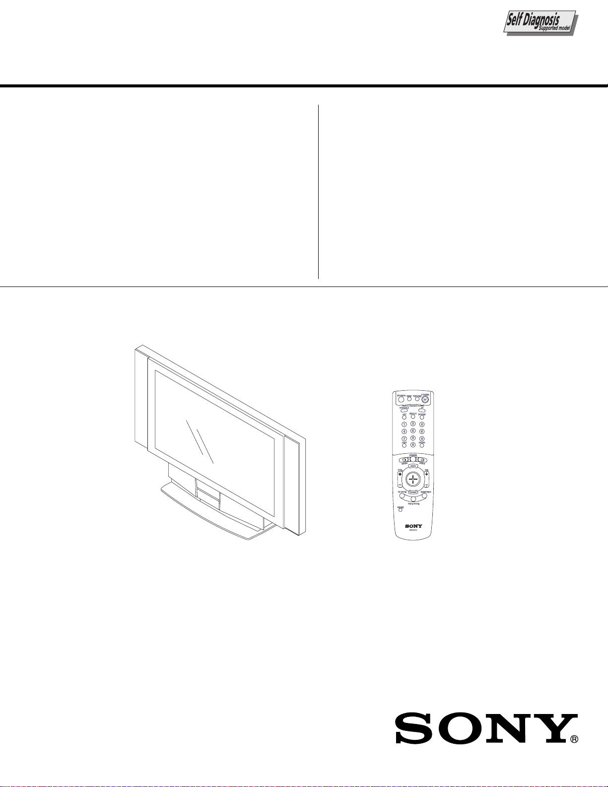
KF-60DX100K
RM-Y910K
Korea
LCD PROJECTION TV

SPECIFICATIONS
Projection System 3 LCD Panels, 1 lens projection system
LCD Panel 1.35 inch TFT LCD panel Approx. 3.15 million dots (1,049,088 pixels)
Projection Lens High Performance, large diameter hybrid lens F2.4
Antenna 75 ohm external terminal for VHF/UHF
Lamp UHP lamp, 100W
XL-2000K
Television System NTSC, American TV Standard
Screen Size (measured diagonally) 60 inches (approx. 152.4 cm)
Channel Coverage
VHF 2-13
UHF 14-69
CATV 1-125
Power Requirements 220V, 60 Hz
Number of Inputs/Outputs
Video (IN) 4 1 Vp-p, 75 ohms unbalanced, sync negative
S Video (IN) 3 Y: 1 Vp-p, 75 ohms unbalanced, sync negative
C: 0.286 Vp-p (Burst signal), 75 ohms
Audio (IN) 6 500 mVrms (100% modulation)
Impedance: 47 kiloohms
AUDIO (VAR/FIX) 1 500 mVrms at the maximum volume setting
(Variable)
500 mVrms (Fixed)
Impedance (output): 2 kiloohms
TV Out 1 Video: 1 Vp-p 75 ohms unbalanced, Sync negative
Audio: 500 mVrms (100% modulation)
Impedance (output): 1 kiloohms
CONTROL S (IN/OUT) 1 minijacks
Component Video Input 2 (Y, PB , PR ) Y: 1.0 Vp-p, 75 ohms unbalanced, sync negative
PB : 0.7 Vp-p, 75 ohms
PR : 0.7 Vp-p, 75 ohms
RF Inputs 2
Converter 1
Speaker Output 15 W × 2
Dimensions (W × H × D) 1,618 × 1,103 × 542 mm
Mass 63 kg
Power Consumption
In Use 220 W
In Standby Under 1 W
Supplied Accessories
Remote Control RM-Y910K
AA Batteries 2 supplied for remote control
Cleaning Cloth 1
Hex key wrench 1
Brackets with screws 2
Optional Accessories
TV Stand SU-60DXK
Lamp XL-2000K
KF-60DX100K
KRM-Y910K
Design and specifications are subject to change without notice.
– 2 –

TABLE OF CONTENTS
Section Title PageSection Title Page
KF-60DX100K
KRM-Y910K
1. SELF DIAGNOSIS FUNCTION
2. DISASSEMBLY
2-1. Rear Cover Assembly ....................................... 8
2-2. OU Bracket Removal ........................................ 8
2-3. Power Block Removal........................................ 8
2-4. Service Position ................................................. 8
2-5. Optical Unit Block Assembly Removal ............ 9
2-6. Terminal Board Assembly Removal.................. 9
2-7. U, M, BB, BC Boards Removal......................... 10
2-8. G Board Removal ............................................... 10
2-9. A Board Removal ............................................... 11
2-10. T Board Removal ............................................... 11
2-11. Control Panel Block Assembly Removal .......... 11
2-12. H3 Board Removal............................................. 11
2-13. H2 Board Removal............................................. 12
2-14. Screen Mirror Block Assembly Removal.......... 12
2-15. H1 Board Removal............................................. 12
3. ELECTRICAL ADJUSTMENTS
3-1. Electrical Adjustment by Remote Commander .... 13
3-1-1. Method of Setting the Service Adjustment
Mode............................................................... 13
3-1-2. Service Mode Adjustment ............................ 13
3-1-3. Memory Write Confirmation Method .......... 13
3-1-4. Adjusting Buttons and Indicator ................... 14
3-1-5. Service Mode List .......................................... 15
3-2. Chassis Picture Quality Adjustment ................. 36
3-2-1. White Level Adjustment ............................... 36
3-2-2. Sub Color/Sub Hue Adjustment .................... 37
3-2-3. Hi-Level/Cut-Off Adjustment ....................... 39
3-3. Vertical Stripe Adjustment ............................... 39
3-4. Sub Bright Adjustment....................................... 40
3-5. Screen Center Adjustment ................................. 40
3-6. Favorites Adjustment ......................................... 40
4. DIAGRAMS
4-1. Block Diagram (1).............................................. 41
Block Diagram (2).............................................. 42
Block Diagram (3).............................................. 43
Block Diagram (4).............................................. 44
Block Diagram (5).............................................. 45
Block Diagram (6).............................................. 46
Block Diagram (7).............................................. 47
Block Diagram (8).............................................. 48
4-2. Frame Schematic Diagram................................. 49
4-3. Circuit Boards Location ..................................... 50
4-4. Schematic Diagrams and Printed Wiring
Boards ................................................................. 50
(1) Schematic Diagram of A (1/3) Board................ 51
(2) Schematic Diagram of A (2/3) Board ............... 52
(3) Schematic Diagram of A (3/3) Board ............... 53
(4) Schematic Diagram of BB (1/9) Board ............. 54
(5) Schematic Diagram of BB (2/9) Board ............. 55
(6) Schematic Diagram of BB (3/9) Board ............. 56
(7) Schematic Diagram of BB (4/9) Board ............. 57
(8) Schematic Diagram of BB (5/9) Board ............. 58
(9) Schematic Diagram of BB (6/9) Board ............. 59
(10) Schematic Diagram of BB (7/9) Board ............. 60
(11) Schematic Diagram of BB (8/9) Board ............. 61
(12) Schematic Diagram of BB (9/9) Board ............. 62
(13) Schematic Diagram of BC (1/3) Board ............. 63
(14) Schematic Diagram of BC (2/3) Board ............. 64
(15) Schematic Diagram of BC (3/3) Board ............. 65
(16) Schematic Diagram of BC4 Board .................... 66
(17) Schematic Diagram of G Board ......................... 67
(18) Schematic Diagrams of H1, H2, H3 and
T Boards ............................................................. 68
(19) Schematic Diagram of M (1/3) Board ............... 69
(20) Schematic Diagram of M (2/3) Board ............... 70
(21) Schematic Diagram of M (3/3) Board ............... 71
(22) Schematic Diagram of U (1/3) Board ................ 72
(23) Schematic Diagram of U (2/3) Board ................ 73
(24) Schematic Diagram of U (3/3) Board ................ 74
– 3 –

Section Title Page
Printed Wiring Boards
• A Board ............................................................ 75
• BB Board.......................................................... 77
• BC Board.......................................................... 79
• BC4 Board........................................................ 80
• G Board ............................................................ 81
• H1 and T Boards .............................................. 83
• H2 Board .......................................................... 84
• H3 Board .......................................................... 85
• M Board ........................................................... 86
• U Board ............................................................ 87
4-5 Waveforms ......................................................... 89
4-6 IC Block Diagrams ............................................. 91
4-7 Semiconductors .................................................. 93
KF-60DX100K
KRM-Y910K
5. EXPLODED VIEWS
5-1. Screen Mirror Block Section ............................ 94
5-2. Cabinet Section................................................... 95
5-3. Main Section....................................................... 96
5-4. Optical Unit Section ........................................... 97
6. ELECTRICAL PARTS LIST ............................ 98
SAFETY-RELATED COMPONENT WARNING!!
COMPONENTS IDENTIFIED BY SHADING AND MARK
¡ ON THE SCHEMATIC DIAGRAMS, EXPLODED
VIEWS AND IN THE PARTS LIST ARE CRITICAL FOR
SAFE OPERATION. REPLACE THESE COMPONENTS
WITH SONY PARTS WHOSE PART NUMBERS APPEAR AS SHOWN IN THIS MANUAL OR IN SUPPLEMENTS PUBLISHED BY SONY.
– 4 –
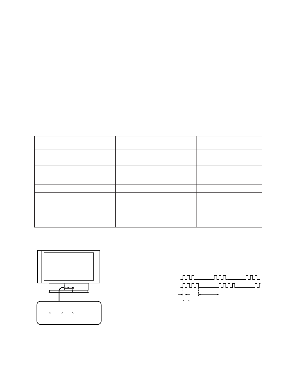
KF-60DX100K
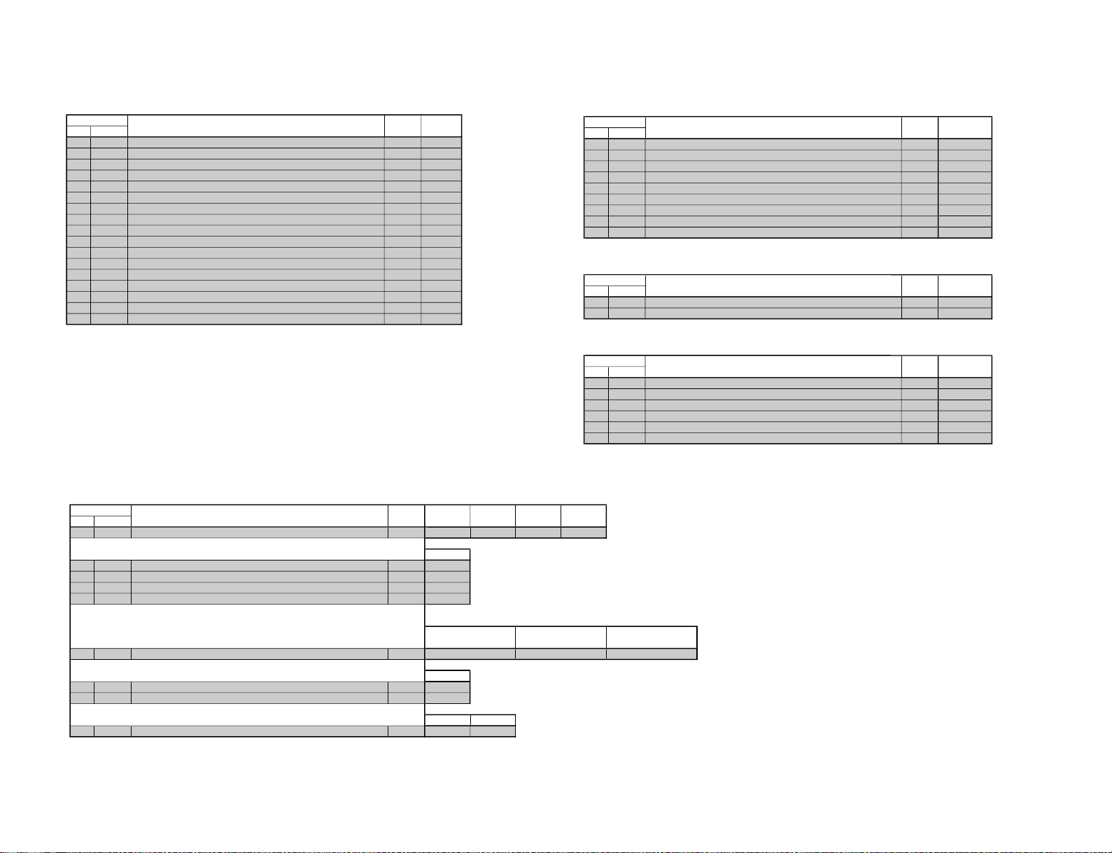
Detected symptoms
Diagnosis Item Probable Cause Location
• Power cord is not plugged in.
• Fuse is burned out (F1601) (G board)
• Power does not come on.
• No power is supplied to the unit.
• AC power supply is faulty.
Power does not turn on
• Lamp cover is not attached securely. • No picture/No soundLamp cover error
• FAN1 or FAN2 power is not supplied. (A board)
• FAN connector is not attached securely.
• No picture/No sound
FAN stopped
Lamp driver error • Lamp driver is faulty. • No picture/No sound
• +5 V is not supplied. (G board) • No picture/No soundLow B error
• Audio ±15 V line is shorted. (A, G board)
• IC1203 or IC1204 is faulty. (A board)
• PS1601 or 1602 is opened. (G board)
Audio error • No picture/No sound
Lamp error • Lamp for the light souce burns out. • No picture/No sound
No. of times
STANDBY/STEREO
indicator blinks
0
3 times
4 times
5 times
6 times
9 times
LAMP LED
flashes
RM-Y910K
SECTION 1
SELF DIAGNOSIS FUNCTION
1. Summary of Self-Diagnosis Function
• This device includes a self-diagnosis function.
• In case of abnormalities, the STANDBY/STEREO indicator automatically blinks. It is possible to predict the abnormality location
by the number of blinks. The Instruction Manual describes blinking of the STANDBY/STEREO indicator.
• If the symptom is not reproduced sometimes in case of a malfunction, there is recording of whether a malfunction was generated or
not. Operate the remote command to confirm the matter on the screen and to predict the location of the abnormality.
2. Diagnosis Items and Prediction of Malfunction Location
• When a malfunction occurs the STANDBY/STEREO indicator only blinks for one of the following diagnosis items. In case of two
or more malfunctions, the item which first occurred blinks. If the malfunctions occurred simultaneously, the item with the lower
blink count blinks first.
• The screen display displays the results regarding all the diagnosis items listed below. The display “ 0 ” means that no malfunctions
occurred.
3. Blinking count display of STANDBY/STEREO indicator
* One blink is not used for self-diagnosis.
•EXAMPLE
<Diagnosis Items> <Number of Blinks>
• Lamp Cover 3 times
STANDBY/STEREOTIMERLAMP
Release of STANDBY/STEREO indicator blinking.
• The STANDBY/STEREO indicator blinking display is released by removing the plug
from the power or leaving for 2 minutes.
• FAN 4 times
Lamp ON : 0.3 seconds
Lamp OFF : 0.3 seconds
– 5 –
Lamp OFF :
3.0 seconds
KF-60DX100K
RM-Y910K
4. Self-Diagnosis screen displays
• In cases of malfunctions where it is not possible to determine the symptom such as when the power goes off occasionally or when the
screen disappears occasionally, there is a screen display on whether the malfunction occurred or not in the past (and whether the
detection circuit operated or not) in order to allow confirmation.
<Screen Display Method>
• Quickly press the remote command button in the following order from the standby state.
DISPLAY b Channel 5 b VOL – b POWER
J
Be aware that this differs from the method of
entering the service mode (volume + ).
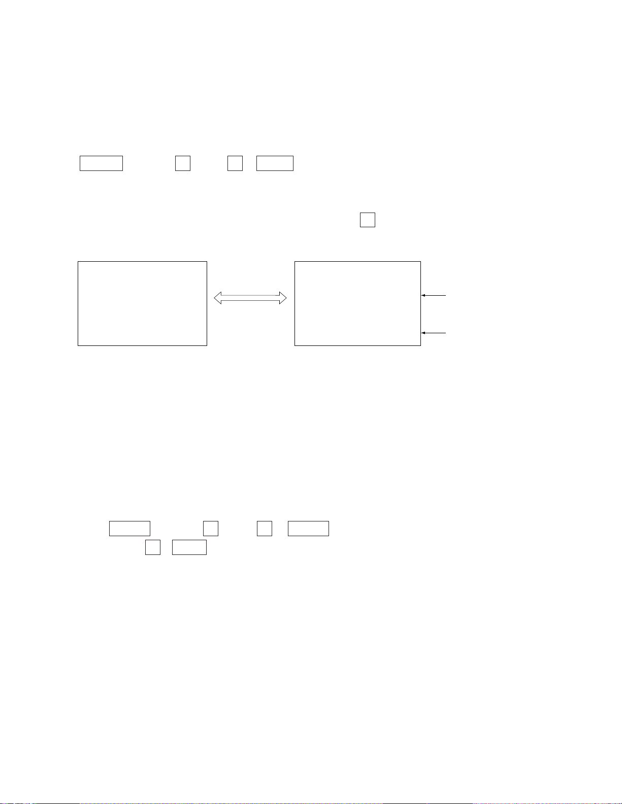
Self-Diagnosis screen display
Self Diagnosis
MAIN
LCD ENGINE
SELF DIAGNOSIS
1:LAMP 1
6:Low B 0
9:AUDIO 1
101:WDT 0
Move the ioystick
B / b
3:LAMP COVER 0
4:FAN 0
5:LAMP DRIVER 0
201:WDT-ENGINE 0
Numeral “1” means a fault was
detected one time or more.
Numeral “0” means that no fault
was detected.
5. Self-Diagnosis Screen Display
• The results display is not automatically cleared. In case of repairs and after repairs, check the self-diagnosis screen and be sure to
return the results display to “ 0 ”.
• If the results display is not returned to “ 0 ” it will not be possible to judge a new malfunction after completing repairs.
<Method of Clearing Results Display>
1. Power off (Set to the standby mode)
2. DISPLAY b Channel 5 b VOL + b POWER (Service Mode)
3. Channel 8 b ENTER (Test reset = Factory preset condition)
<Method of Ending Self-Diagnosis Screen>
• When ending the self-diagnosis screen completely, turn the power switch OFF on the remote commander or the main unit.
– 6 –

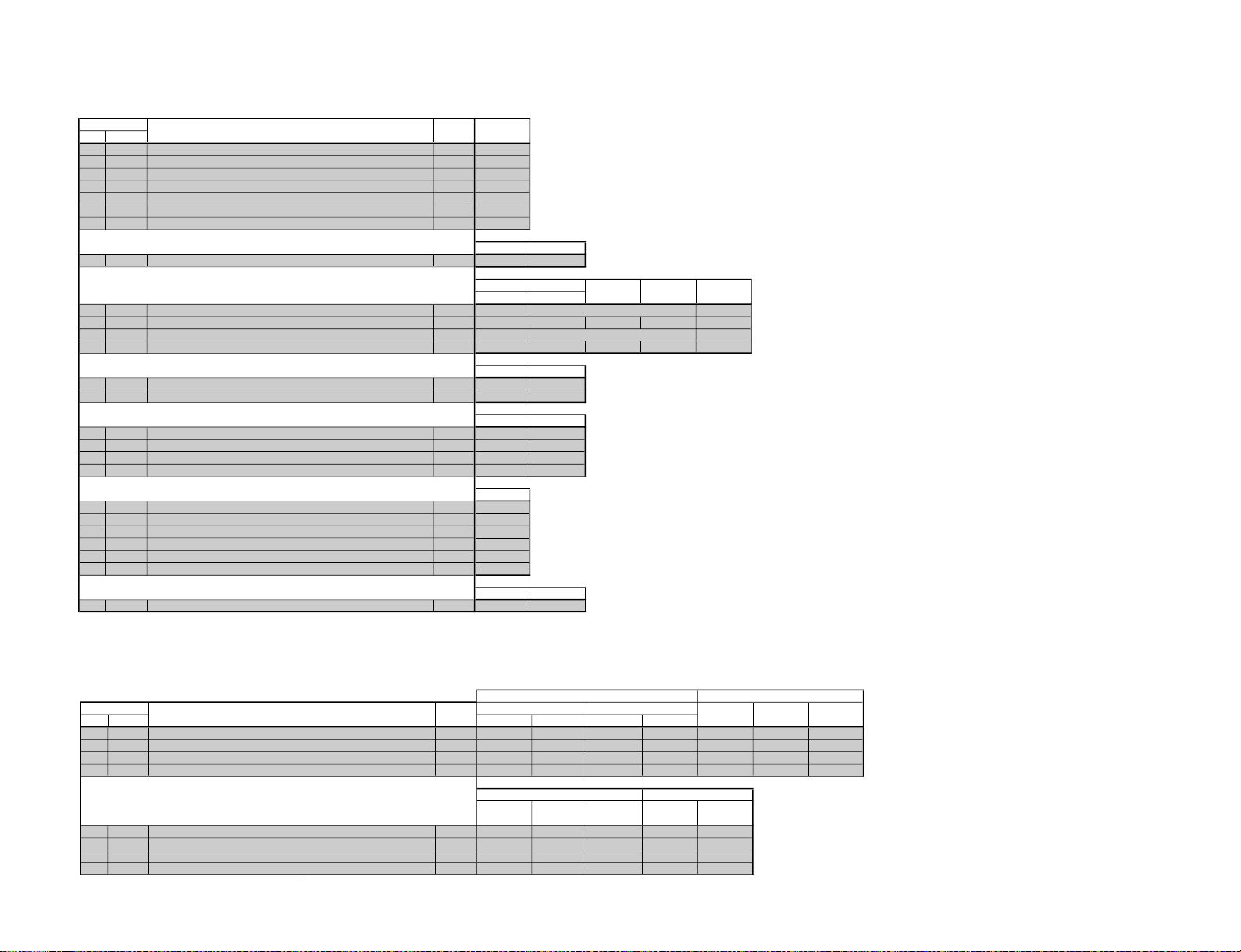
KF-60DX100K
24 AUDIO PROT
43 LOW B ERR
D1902
CN1908
D1901
M board
A board
T board
IC9004
MAIN CPU
+5V DETECT
LAMP
DRIVER
LAMP
HV DETECT
FAN1
FAN2
IC9502
LCD ENGINE
+5V
LAMP DRV
HV DET
LAMP PROT
28
FAN PROT 24
LAMP PROT 29
3. Lamp Cover
LAMP COV
HV DET
LAMP PRT
FAN1 PR
FAN2 PR
4. FAN Stop
9. Audio
6. Low B
LAMP COV 27
Q9505,9507-9509
S8001
DC DETECT
Q1211, 1213,1215
IC9005
AUDIO AMP
IC1203, 1204
4
12
3
8
10
6. Self-Diagnosis function operation
3 : Lamp Cover When lamp cover SW is opened then pin 4 of CN1908 on the A board is high, LCD Engine µ-com (IC9502)
detects it and make turn off the lamp.
4 : FAN Stop When FAN1 or FAN2 is stopped then pin 8 or q; of CN1908 on the A board is high, LCD Engine µ-com
(IC9502) detects it and make turn off the lamp.
5 : Lamp Driver When lamp is not turned on then pin wl of LCD Engine µ-com (IC9502) is high, checks pin wk of LCD Engine
µ-com . If pin wk is low, it is judged no High Voltage.
6 : Low B Detect +5 V line failure.
9 : Audio When DC is appeared by audio amp failure at speaker line.
Then it is detected by MAIN µ-com (IC9004) and it turns off the main power.
LAMP : Lamp error When lamp is not turned on then pin wl of LCD Engine µ-com (IC9502) is high, checks pin wk of LCD Engine
µ-com. If pin wk is high, it is judged lamp is burned out.
Self-Diagnosis block diagram
RM-Y910K
– 7 –
SECTION 2
3 Three screws
(+BVTP 3 x 12)
7 Power block
6 Ballast
bracket
4 Ballast cover
5 Two screws
(+BVTP 3 x 12)
1
2 Two screws
(+BVWHTP 3 x 12)
2 Cabinet stay (L)
1 Screw
(+BVTP 4 x 16)
3
DISASSEMBLY
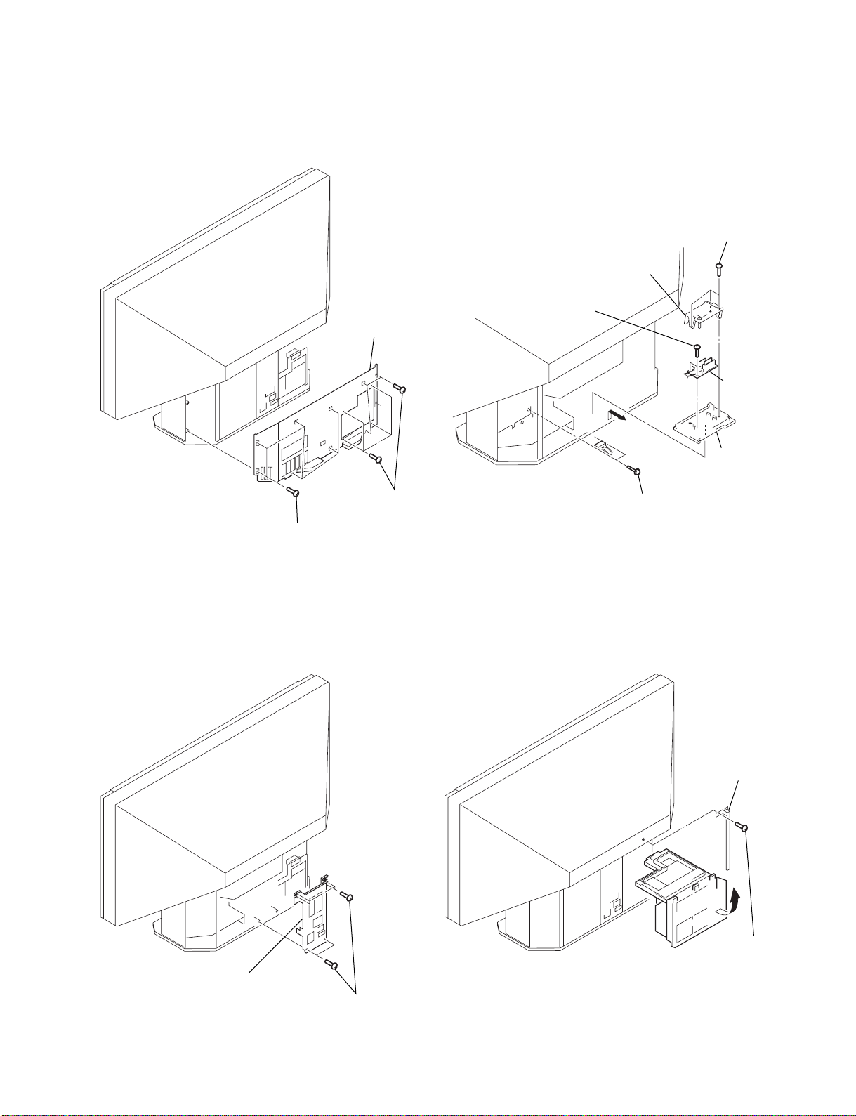
2-1. REAR COVER ASSEMBLY 2-3. POWER BLOCK REMOVAL
2 Rear cover
assembly
KF-60DX100K
KRM-Y910K
2-2. OU BRACKET REMOVAL 2-4. SERVICE POSITION
1 Eight screws
(+BVTP 4 x 16)
1 Six screws
(+BVTP 4 x 16)
2 OU bracket
1 Six screws
(+BVTP 4 x 16)
– 8 –
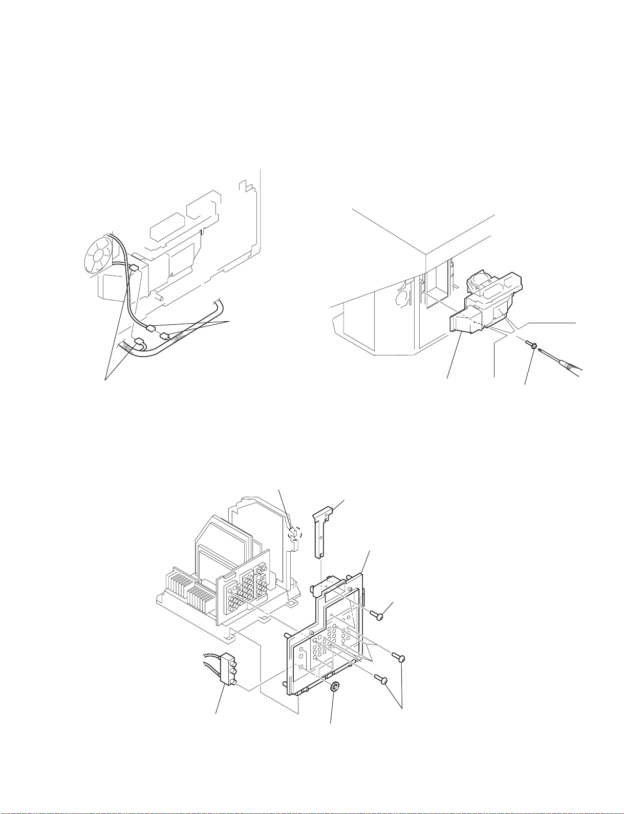
2-5. OPTICAL UNIT BLOCK ASSEMBLY REMOVAL
3 Optical unit block
assembly
2 Loosen two screws,
which can not taken
apart from the assy.
Note: Be careful about the no dust or dirt are on the surface
contacts the optical unit block assembly.
• Clean the periphery of the set.
• Clean the periphery of the optical unit block assembly in
the set (the inside of the control panel, the surface contacts
between the optical unit block assembly and the bottom
cabinet and periphery).
1 Connector
KF-60DX100K
KRM-Y910K
1 Connector
2-6. TERMINAL BOARD ASSEMBLY REMOVAL
6 Claw
2 Bracket M
7 Terminal board
assembly
1 Two screws
(+BVTP 4 x 16)
5 RF antenna switch
4 Two washers
– 9 –
3 Seven screws
(+BVTP 3 x 12)
2-7. U, M, BB, BC BOARDS REMOVAL
3 BB board
2 M board
KF-60DX100K
KRM-Y910K
4 BC board
1 U board
2-8. G BOARD REMOVAL
4 G bracket assembly
3 Three screws
(+BVTP 3 x 12)
5 G board
1 Screw (+BVTP 4 x 16)
2
– 10 –
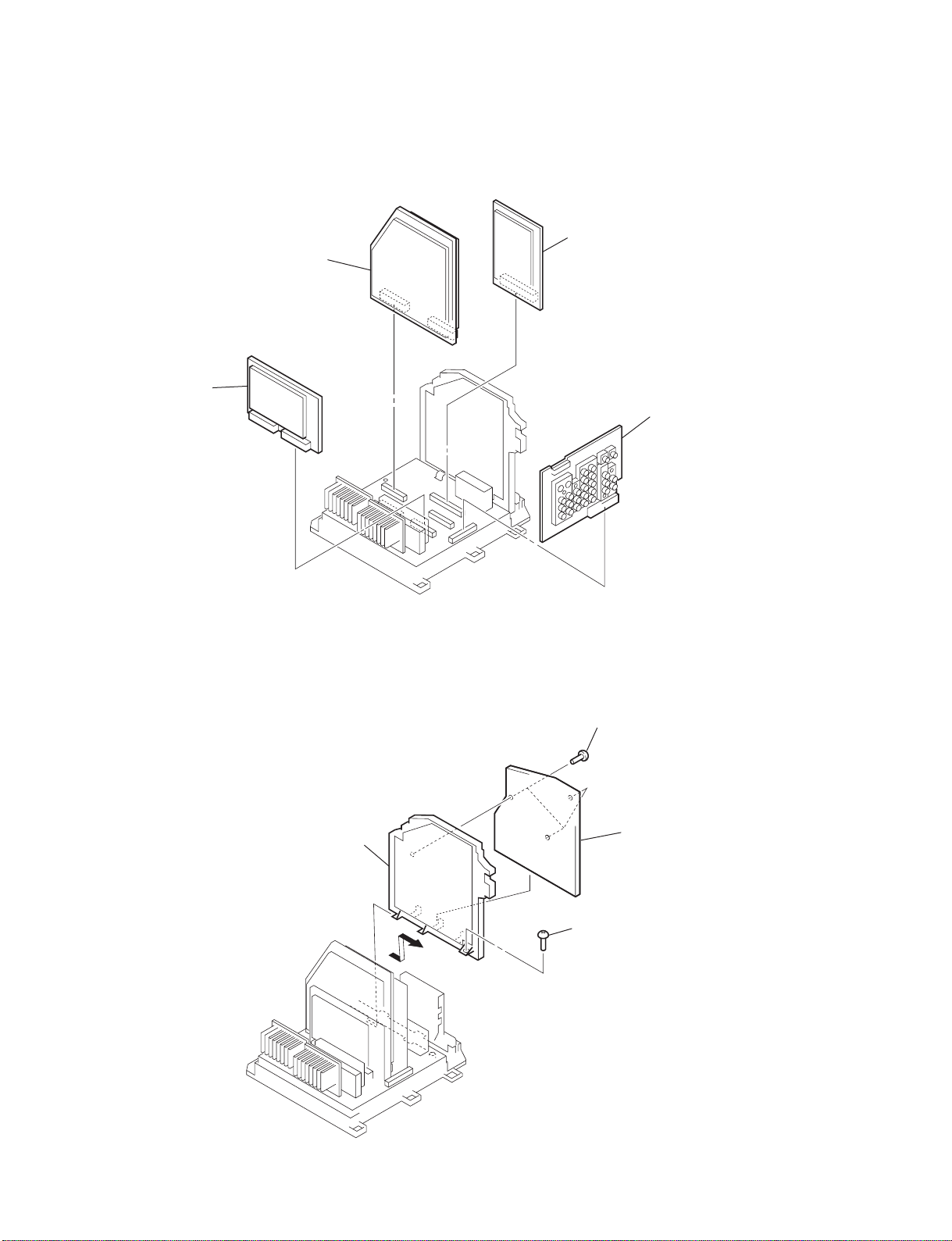
KF-60DX100K
1 Four strikes
5 Six screws
(+BVTP 4 x 16)
3 Four strikes
6 Control panel
assembly
4 Front cover (R)
assembly
2 Front cover (L)
assembly
KRM-Y910K
2-9. A BOARD REMOVAL
3 A board
2-11. CONTROL PANEL BLOCK ASSEMBLY
REMOVAL
1 Two screws
(+BVTP 3 x 12)
2 Two claws
2-10. T BOARD REMOVAL 2-12. H3 BOARD REMOVAL
3 Connector
5 H3 board
2 T board
1 Screw (+BVTP 3 x 12)
4 Control panel block
2
1 Four screws
(+BVTP 3 x 12)
– 11 –
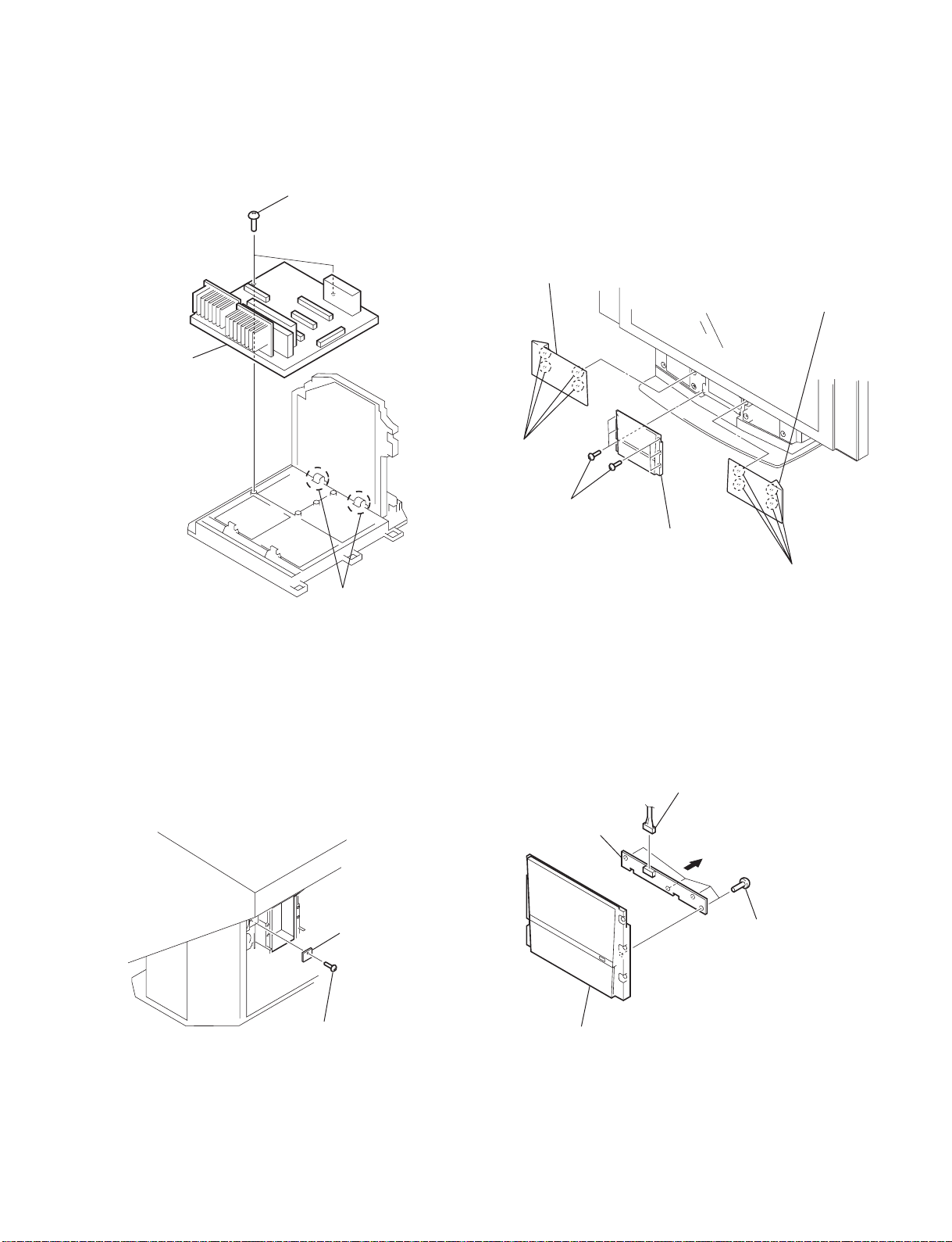
KF-60DX100K
2 H1 lid
1 T wo claws
6 T wo screws
(+BVTP 3 X 12)
3 T wo screws
(+BVTP 4 X 16)
4 Fasten tag
5 Three connectors
7 H1 board
KRM-Y910K
2-13. H2 BOARD REMOVAL
3 Three screws
(+BVTP 3 x 12)
6 H2 board
5 Connector
4
2 Claw
1 Open the H2 bracket
assembly
2-15. H1 BOARD REMOVAL
2 Claw
2-14. SCREEN MIRROR BLOCK ASSEMBLY
REMOVAL
Screen mirror block
assembly
4
2 Four screws
(+BVTP 4 x 16)
1 Connecotr
3 Four screws
(+BVTP 4 x 16)
– 12 –
SECTION 3
* : LCD Projector Engine
3D-COMB
MCP-ADJ3
MID1
* L001AOI
CCD
OP
* D-GM TG
ID
2103-1
VID ADJ
MID2
* L001POS S
* L001OUT
* D-GM IM
2103-2
USER STD
* HV POS AD
MID3
* L001SCALE
* H POS SHI
P-BOOST1
MCP-FIX
MID5
* L001ENH
* SH SET
* PLL-C
* L001Y
P-BOOST2
2151
MID6
* LCD-DR
* D-GM WB
* L001IN
P-BOOST3
AP
OSD
* LM75
* D-GM TEST
TRUS
* L001OPT
MCP-ADJ1
SNNR
* OSD-E
* D-GM TPN
DLBY
* L001OACT
ID1
* OPTION-E
MCP-ADJ2
* D-GM CUR
ELECTRICAL ADJUSTMENTS
KF-60DX100K
RM-Y910K
3-1. ELECTRICAL ADJUSTMENT BY REMOTE
COMMANDER
By using remote commander (RM-Y910K), all circuit adjustments can be made.
NOTE : Test Equipment Required.
1. Pattern Generator (with component outputs)
2. Oscilloscope
3. Digital multimeter
3-1-1.Method of Setting the Service Adjustment
Mode
1. Standby mode. (Power off)
2. DISPLAY t 5 t VOL (+) t TV POWER
on the remote commander.
(Press each button within a second.)
The following service screen will appear.
Category Name
Item No.
3D-COMB 0 0 SERVICE
NRMD TV
WSL: xxx
Mode
Data
3-1-2.Service Mode Adjustment
1. The SCREEN displays the item being adjusted.
2. Press “1” or “4” on the remote commander to select the
adjustment item.
3. Press “3” or “6” on the remote commander to change the data.
4. Press “2” or “5” on the remote commander to select the category.
Every time you press “2” (Category up), Service mode
changes in the order as shown below.
Item Name
Item Name Input Signal
F/A FLAG: xxxxxxxx
CBA FLAG: xxxxxxxx
Category Name
L001OUT 0 0 G
OCKPN
TEMP 42DEG
LCD PJ ENGINE VER.0.026
<LCD PROJECTOR ENGINE>
Item No.
Data
9/11
EE2F
5. If you want to recover the latest values press “-” then
“[ENTER]” to read the memory.
6. Press “[MUTING]” then “[ENTER]” to write into memory.
7. Turn power off.
Note: Press “8” then “[ENTER]” on the remote commander to
set the shipping conditions or turn set off and on to exit.
3-1-3. Memory Write Confirmation Method
1. After adjustment, turn power off with the remote commander.
2. Turn power on and set to service mode.
3. Call the adjusted items again and confirm they were adjusted.
– 13 –

KF-60DX100K
RM-Y910K
3-1-4. Adjusting Buttons and Indicator
MUTING
Write data to NVM
DISPLAY
Adjustment category
Adjustment item
up
Adjustment item
down
Initialize data
(Not stored)
User control goes
to the standerd state
(Shipping Conditions)
VOL +
PICTURE MODE
WIDE MODE
K
up
Data up
Data down
Adjustment category
down
Read data from
NVM
POWER
ENTER
TWIN
FAVORITES
FUNCTION OF KEYS ON COMMANDER
• 1 : Changes adjustment item. (item No. moves up)
• 4 : Changes adjustment item. (item No. moves down)
• 2 : Changes adjustment category.
(category moves up)
• 5 : Changes adjustment category.
(category moves down)
• 3 : Changes data value. (up)
• 6 : Changes data value. (down)
Commander Function
Button Mode Description
[MUTING] + [ENTER] WRITE Writes data to NVM.
- + [ENTER] READ Reads data from NVM.
8 + [ENTER] RESET Set the shipping condition.
7 + [ENTER] INT– Service data initialization.
Not stored.
(Be sure not to use usually)
RM-Y910K
– 14 –

3-1-5.Service Mode List
3D-COMB
Table 1
No. Name
0 NRMD Noise reduction mode setting 0 - 3 Table 1
1 YAPS Y output correction 0 - 3 3
3D (COMB)
3L (THROUGH)
3L (ROUND)
3L (THROUGH) COMB/ROUND
THROUGH ROUND THROUGH
2 CLKS System clock setting 0 - 3 1
28NR=01010101
3 NSDS Selection for standard/non-standard signal processing 0 - 3 Table 1 3 (when OP=0)
4 MSS Selection for inter-frame/inter-line processing 0 - 3 0 2 (when OP=1)
5 KILS Killer processing selection 0 - 3 2 3 NSDS 03030303
6 CDL C-signal phase with respect to the Y-signal 0 - 7 Table 5
7 DYCO DY detection coring level (Y motion detection coring) 0 - 15 Table 2
8 DYGA DY detection gain (Y motion detection gain) 0 - 15 Table 2
Table 2
9 DCCO DC detection coring level (C motion detection coring) 0 - 15 Table 2
3DYC 2DYC + YCNR MNNR YCNR
10 DCGA DC detection gain (C motion detection gain) 0 - 15 Table 2
0 NRMD= 0123
11 YNRL Frame recursive YNR nonlinear filter limit level 0 - 3 1 7 DYCO 2224
12 CNRL Frame recursive CNR nonlinear filter limit level 0 - 3 1 8 DYGA 10 10 10 10
13 VTRH Hysteresis for H sync non-standard signal detection 0 - 3 Table 3 9 DCCO 5535
14 VTRR Sensitivity for H sync non-standard signal detection 0 - 3 Table 3 10 DCGA 5 5 10 5
15 LDSR Sensitivity for frame non-standard signal detection 0 - 3 Table 3 25 D2GA 4444
16 VAPG V aperture compensation gain 0 - 7 Table 6
17 VAPI V aperture compensation convergence point 0 - 31 Table 6
18 YPFT Y peaking filter (BPF) center frequency 0 - 3 3
Table 3
19 YPFG Y peaking filter (BPF) gain 0 - 15 7
RF Video (CV/S) Component
20 YHCO Y output high frequency component coring 0 - 3 0 13 VTRH 1 1 1
21 YHCG Y output high frequency component coring gain 0 - 1 0 14 VTRR 1 1 1
22 HSSL H sync slice level 0 - 15 12 15 LDSR 2 2 2
23 VSSL V sync slice level 0 - 15 8 35 CC3N 0 0 0
24 ADCL ADC clock delay 0 - 3 3
25 D2GA Moving detection gain 0 - 7 Table 2
26 KILR Killer detection reference 0 - 15 3
Table 4
27 OP Option : Selection of comb filter & recursive noise reduction types 0 - 1 1
RF
Video (1,2,3,4)
Video (5,6)
28 NR1 Noise reduction on/off 0 - 1 Table 1 41 LIND 0 0 2
29 NR2 SNNR control on/off 0 - 1 0
30 WSL Noise level detection level data 0 - 255 Read
31 HPLL H PLL filter 0 - 1 1
Table 5
32 BPLL Burst PLL filter 0 - 1 1
RF Video (CV/S)
33 FSCF Burst extraction gain 0 - 1 0 6 CDL 3 3
34 PLLF PLL loop gain 0 - 1 1
35 CC3N Selection if a line comb filter C separation filter characteristic 0 - 1 Table 3
36 HDP Fine adjustment of the system H phase 0 - 7 5
Table 6
37 BGPS Burst gate start 0 - 15 4
VIVID STANDARD MOVIE MILD
38 BGPW Burst gate width 0 - 15 10 16 VAPG 0330
39 TEST Test bit (0 : Normal mode, 1 : Test mode) (*forbidden setting) 0 - 1 0 17 VAPI 6 10 10 4
40 WSC Amount of noise detection coring 0 - 3 1
41 LIND DRC-M line doubling setting for non-standard signal UHF/VHF & Video 1-4 0 - 15 Table 4
42 PFGO YPFG offset at GR on (*not used) 0 - 7 3
Data
Range
Data
Item
Function
2330 NRMD 0011
RF/Video S Video
Non-standard Standard Non-standardStandard
Note: • shaded items are fixed. There is no need to change data. Others are different a little
in the sets individually. Basically, there is no need to change data, too.
– 15 –
KF-60DX100K
RM-Y910K

2103-1
One screen (Mild) Others
No. Name
0 YLEV Y out gain 0 - 63 45 50 28 33
1 CLEV Cb & Cr out gain 0 - 63 35 58 13 31
RF Video
2 SCON Sub contrast 0 - 15 8 9
3 SCOL Sub color 0 - 15 6 7
4 SHUE Sub hue 0 - 15 9 8
5 YDLY Y/C delay time 0 - 3 0 0
6 SHAP Sharpness 0 - 15 5665
7 SHF0 Sharpness f0 selector 0 - 31222
8 PREO Shapeness pre/over-shoot ratio 0 - 30330
9 BPF0 Chroma band filter f0 setting 0 - 33000
10 BPFQ Chroma band filter Q setting 0 - 30000
11 BPSW Chroma band filter on/off 0 - 11000
12 TRAP Y block chroma trap filter on/off 0 - 10000
13 LPF Y/Cb/Cr output LPF on/off 0 - 11111
14 AFCG AFC loop gain (PLL between H sync & H VCO) 0 - 1 1 0 0
15 CDMD V countdown system mode selector 0 - 3333
16 SSMD H & V sync slide level setting 0 - 3 0 0 0
17 HMSK Masking of macrovision signal on/off 0 - 1 1 1 1
18 HALI H automatic adjustment on/off 0 - 1 0 0 0
19 PPHA H TIM phase adjustment video 0 - 15 6 8 8
One screen (Mild) Others
20 CBOF Cb/EXT Cb offset 0 - 63 32 34 36 36
21 CROF Cr/EXT Cr offset 0 - 63 32 31 33 33
One screen
Others
03
Movie
02
Movie
Component
(480i)
RF Video
Component
(480i)
RF/Video
Component
(480i)
RF/Video
Component
(480i)
RF/Video
Component
(480i)
RF
Composite
Video
S Video
Component
(480i)
Item
Function
Data
Range
RF/Video
0
23 DCTR DC transmission ratio 0 - 3
0
22 ATPD Auto-pedestal inflection point 0 - 3
– 16 –
KF-60DX100K
RM-Y910K
– 17 –
2103-2
RF/Video
No. Name VDO DRC
0 YLEV Y out gain 0 - 63 26 22
1 CLEV Cb & Cr out gain 0 - 63 23 16
RF Video
2 SCON Sub contrast 0 - 15 8 12
3 SCOL Sub color 0 - 15 6 6
4 SHUE Sub hue 0 - 15 9 8
5 YDLY Y/C delay time 0 - 3 0 0
6 SHAP Sharpness 0 - 15 6 6 6
7 SHF0 Sharpness f0 selector 0 - 3 1 1 1
8 PREO Shapeness pre/over-shoot ratio 0 - 3 0 3 3
9 BPF0 Chroma band filter f0 setting 0 - 3 0 0 0
10 BPFQ Chroma band filter Q setting 0 - 3 0 0 0
11 BPSW Chroma band filter on/off 0 - 1 0 0 0
12 TRAP Y block chroma trap filter on/off 0 - 1 0 0 0
13 LPF Y/Cb/Cr output LPF on/off 0 - 1 1 1 1
RF Video
14 AFCG AFC loop gain (PLL between H sync & H VCO) 0 - 1 1 0
15 CDMD V countdown system mode selector 0 - 3 3 3
16 SSMD H & V sync slide level setting 0 - 3 0 0
17 HMSK Masking of macrovision signal on/off 0 - 1 1 1
18 HALI H automatic adjustment on/off 0 - 1 0 0
19 PPHA H TIM phase adjustment video 0 - 15 6 8
RF/Video
VDO DRC
20 CBOF Cb/EXT Cb offset 0 - 63 32 36
21 CROF Cr/EXT Cr offset 0 - 63 33 34
Data
22 ATPD Auto-pedestal inflection point 0 - 3 *1
23 DCTR DC transmission ratio 0 - 3 *1 *1 The same data as 2103-1.
Composite
Video
S Video
Item
Function
Data
Range
RF
KF-60DX100K
RM-Y910K
P- BOOST 1
Table1
No. Name Vivid Standard Movie Mlid
0 BSET 0 - 7 Table1 RF 2464
1 AMS Amplitude mode selection
Data table selection
0 - 11 Video5767
2 DEMO
Demonstration mode on/off
0 - 1 0 Component 1363
3 SN Steepness correction 0 - 63- 0000
P- BOOST 2
No. Name 01234567
0 LWID Line width correction 0 - 630 31313131313131
1 STEP 0 - 6300000000
2 CRNG Coring level
Steeness correction
0 - 63 0 15 25 10 30 25 5 25
3 VDC Video dependent coring on/off 0 - 101111111
4 OSP Overrrule smart peaking 0 - 100100000
5 BOST Black offset compensation on/off 0 - 100000000
6 ABST Adaptive black stretch 0 - 6300000000
7 VGAM Variable gamma 0 - 63 32 28 24 24 22 22 31 22
8 NLMP Non-linearity amplifier 0 - 63 0 22 25 21 15 22 7 18
9 PKNG Peaking amplitude 0 - 63 0 37 20 32 25 15 20 22
10 CFS Contour filter selection 0 - 101111111
11 FHS Line frequency selection 0 - 100000000
12 LDH Luminance determined histogram
Snow color adjustment by green stretch
0 - 101111111
13 SNOW 0 - 111111111
Common
14 WLB Window letterbox format 0 - 1 0
P- BOOST 3
No. Name 01234567
0 CDS Color dependent sharpness on/off 0 - 111111111
1 CTI Color transient improvement on/off 0 - 100000000
2 WPO White-point stretch on/off 0 - 111111111
3 DBL Blue stretch on/off 0 - 100000000
4 GBL Blue stretch gain 0 - 100000000
5 SBL Blue stretch size 0 - 100000000
6 DSK Dynamic skin tone on/off 0 - 100000000
7 ASK Dynamic skin tone angle 0 - 100000000
8 WSK Dynamic skin tone width 0 - 100000000
9 SSK Dynamic skin tone size 0 - 100000000
10 DGR Green enhancement on/off 0 - 101100100
11 GGR Green enhancement gain 0 - 100000000
12 WGR Green enhancement width 0 - 100000000
13 SGR Green enhancement size 0 - 100000000
14 CDLY Chrominance delay 0 - 747777454
BSET data (P-BOOST1 _0_BSET= )
Two screen
SCREEN MODE
Data
One screen
Item
Function
Data
Range
BSET data (P-BOOST1 _0_BSET= )
Item
Function
Data
Range
Item
Function
Data
Range
– 18 –
KF-60DX100K
RM-Y910K

– 19 –
RF / Video Component
480i 480i 480p/720p 1080i
No. Name Mild Others Mild Others All mode All mode
0 RDRV RED drive gain control 0 - 63 50 50 50 50 50 50
1 RCUT
RED cutoff control
0 - 63 40 40 40 40 40 40
2 GDRV
GREEN drive gain control
0 - 63 50 50 50 50 50 50
3 GCUT
GREEN cutoff control
0 - 63 40 40 40 40 40 40
4 BDRV
BLUE drive control
0 - 63 50 50 50 50 50 50
5 BCUT
BLUE cutoff control
0 - 63 40 40 40 40 40 40
6 CROF
DC offset for Cr signal
0 - 15999967
7 CBOF
DC offset for Cb signal
0 - 15777767
8 SCON
Sub contrast gain control
0 - 15444455
9 SBRT
Sub brightness control
0 - 63 31 31 31 31 31 31
10 PICT
Picture gain control
0 - 63 53 53 50 50 50 50
11 BRT
Brightness control
0 - 63 55 55 55 55 55 55
Component
No. Name 480i 480p 720p 1080i Neutral Warm Neutral Warm
0 SCOL Color gain control 0 - 15777877 ---1 SHUE Hue center control 0 - 15888887 ---2 RYR
Sets +(R-Y) component in R-Y axes
0 - 15222244 0
000
3 RYB
Sets -(B-Y) component in R-Y axes
0 - 15 10 10 10 10 12 12
+4 +4 0 0
4 GYR
Sets -(R-Y) component in G-Y axes
0 - 15 10 10 10 12 10 10
0000
5 GYB
Sets -(B-Y) component in G-Y axes
0 - 15888555
0000
MCP-ADJ3
No. Name Mild Others Mild Others Mild Others Mild Others Mild Others Mild Others
0 SSHP Sharpness center control 0 - 3110000010100
1F0
Sets sharpness f0
0 - 3131313133333
2 POVR
Sets the preshoot to overshoot ratio
0 - 3131322222222
3 SYSM
Sets signal bandwidth
0 - 3111112111122
4 CTI Sets edge improvement of color difference signal 0 - 3000001010001
Shift value of HD
system
7
4
31
Twin , Favorite, Index,
Freeze
53
55
Video
Item
Function RF
Twin , Favorite, Index,
Freeze
VideoRF
480i 480p
Item
Function
Data
Range
Item
Function
Data
Range
Data
Range
40
50
40
9
Twin , Favorite, Index,
Freeze
50
40
50
0
10
8
7
9
2
10
720p 1080i
Component
3
0
2
1
MCP-ADJ1
MCP-ADJ2
KF-60DX100K
RM-Y910K
– 20 –
Component
480i
No. Name Vivid Standard Movie Mild Vivid Standard Movie Mild Vivid Standard Movie Mild
0 LTI
Sets edge improvement of brightness signal
0 - 3000000000000
1 GAM
Gamma offset control
0 - 15617111712171
2 DCTN
Sets Y-system DC transmission rate
0 - 3110111011101
3 DPIC
Dynamic picture control
0 - 3110111011101
15 14 13 12 3 2 1 0 7 6 5 4
15 14 13 12 3 2 1 0 7 6 5 4
Component
480p 720p 1080i
Vivid Standard Movie Mild Vivid Standard Movie Mild Vivid Standard Movie Mild
0 LTI
Sets edge improvement of brightness signal
0 - 3000000000000
1 GAM
Gamma offset control
0 - 154312361716171
2 DCTN
Sets Y-system DC transmission rate
0 - 3110111011101
3 DPIC
Dynamic picture control
0 - 3210121012101
11 10 9 8 19 18 17 16 15 14 13 12
111098--------
Vivid Standard Movie Mild Vivid Standard Movie Mild
0 LTI
Sets edge improvement of brightness signal
0 - 300000000
1 GAM
Gamma offset control
0 - 1562726272
2 DCTN
Sets Y-system DC transmission rate
0 - 300000000
3 DPIC
Dynamic picture control
0 - 300000000
23 22 21 20 23 22 21 20
--------
4
Item
Function
MIDE
Sets MID enhancement
0 - 31
0 - 31
Zoom / Caption
RF Video
0 - 31
Full / Normal
Full / Normal
Data
Range
4 MIDE
Sets MID enhancement
4 MIDE
Sets MID enhancement
Zoom / Caption
Twin Picture , Freeze, Favorite Index
Full / Normal
Zoom / Caption
VID ADJ
USER STD
*In case of USER RESET or TEST RESET, write in data of USER STD
No. Name Vivid Standard Movie Mild
0 UPIC Picture 0 - 63 63 48 31 48 63 48 31 48
1 UBRT Brightness 0 - 63 17 26 21 26 17 26 21 26
2 UCOL Color gain control 0 - 63 31 31 35 31 31 31 35 31
3 UHUE
Hue control
0 - 63 31 31 31 31 31 31 31 31
4 USHP
Sharpness gain control
0 - 63 37 37 31 31 37 37 31 31
5 UHWT
Dynamic color on/off
0 - 1 0 0 0 0 2101
6 UTMP Color temperature (9 : Warm, 1 : Neutral, 2 : Cool) 0 - 3 2 1 0 1
480i 480p
Vivid Standard Movie Mild Vivid Standard Movie Mild Vivid Standard Movie Mild Vivid Standard Movie Mild
7 UPOF Offset for UPIC (picture cliarity adjustment) 0 - 31 - 63 33 35 33 35 31 35 33 33 28 33 31 33 27 34 27 34
8 UBOF Offset for UBRT (Picture cliarity adjustment) 0 - 31 - 63 30 36 32 37 32 34 32 34 31 31 32 31 38 36 32 36
9 UCOF Offset for UCOL (Picture cliaruty adjustment) 0 - 31 - 63 34 29 31 27 32 32 34 31 33 31 31 31 36 35 27 35
10 UHOF Offset for UHUE (Picture cliarity adjustment) 0 - 31 - 63 31 31 33 31 34 34 31 34 31 31 28 31 31 31 28 31
11 USOF Offset for USHP (Picture cliarity adjustment) 0 - 31 - 63 40 35 38 38 38 42 37 31 28 31 31 31 33 43 40 31
Component
720p 1080i
Vivid Standard Movie Mild Vivid Standard Movie Mild Vivid Standard Movie Mild
7 UPOF Offset for UPIC (picture cliarity adjustment) 0 - 31 - 63 29 33 31 33 31 31 31 31 31 34 36 34
8 UBOF Offset for UBRT (Picture cliarity adjustment) 0 - 31 - 63 31 36 32 36 31 36 32 36 32 37 29 37
9 UCOF Offset for UCOL (Picture cliaruty adjustment) 0 - 31 - 63 34 29 31 29 34 29 31 29 35 31 30 31
10 UHOF Offset for UHUE (Picture cliarity adjustment) 0 - 31 - 63 31 31 28 31 31 31 28 31 31 31 33 31
11 USOF Offset for USHP (Picture cliarity adjustment) 0 - 31 - 63 31 31 31 31 31 31 31 31 31 37 31 25
*set 31 in the center, and shift to USER DATA
*About color, if USER DATA becomes 0, data of CXA2101_COLOR becomes 0 compulsorily
Function
Data
Range
Vivid
RF
Standard Movie Mild
Picture
Twin Picture , Freeze, Index , Favorite
Brightness
Color
Hue
Sharpness
Color Temp
Video
Component
KF-60DX100K
RM-Y910K
– 21 –
MCP-FIX
No. Name
0 RON
Turns on/off RED video output not including reference pulse
0-1
1 (*1)
1 GON
Turns on/off GREEN video output not including reference pulse
0-1 1 (*1) *1 Don't memorize
2 BON
Turns on/off BLUE video output not including reference pulse
0-1 1 (*1)
3 CBLK
Turns on/off H, V blanking for RGB outputs
0-1 0
4 AKBT
Selects the timing pulse that generates reference pulse
0-1 1
5 BLKS
Selects H, V blanking system for RGB outputs
0-1 1
6 LIMI
Limiter to excess input
0-3 0
7 YSYM
Sets valid/invalid to the input pin YS/YM-1
0-1 0
8 YMVM
Turns on/off MUTE function for VM OUT in YM ON section
0-1 0
9 CLPS
Selects color difference input pin offset control pulse
0-1 1
10 CLPM
Changes over clamp pulse width
0-3 0
11 ABLM
Changes over ABL mode
0-3 0
12 ABLT
Adjusts threshold voltage to the input of ABL IN pin
0-3 0
13 HSMA
Sets whether H sync is added to V sync at HS-OUT and SELH-OUT
0-1 1
14 LRGB
Picture level control in LRGB2 system
0-15 15
15 PABL
Sets level detection DC at RGB-OUT of PEAK-ABL
0-15 15
16 BLKB
RGB-OUT bottom limiter level control
0-15 5
Item
Function
Data
Range
Data
2151
No. Name
0 MTRX Matrix out 0 - 3 0011
COMMON
1 GAIN
Gain select
0 - 3 0
2 CBGN
Cb gain
0 - 15 9
3 VTC
V TC
0 - 3 1
4 HWID
H width
0 - 3 1
5 HSEP
HSEP select
0 - 1
COMMON
6 TEST
Test
0 - 1 0
7 FRGB 0 - 1 0
1080i Others
8 HMSK
H sync masking in vertical retrace
0 - 1 0 1
Video 6
(480i, 480p, 720p, 1080i)
111
RF/Video 1, 2, 3, 4
(Video 5, 6 no signal)
Video 5
(480i, 480p, 720p, 1080i)
31.5 kHz 33.75 kHz 45 kHz
Item
Function
Data
Range
15.75 kHz
AP
No. Name
0 SVOL Volume offset for volume 0 - 15 0
1 SBAL Balance offset for balance 0 - 15 7
2 SBAS Bass offset for bass 0 - 15 3
3 STRE
Treble offset for treble
0 - 15 4
4 BBLP
BBE low pass filter
0 - 15 13
5 BBHP
BBE high pass filter
0 - 15 10
6 SREF
Surround effect
0 - 15 11
7 AGC
Auto gain control
0 - 1 0
8 BBE
BBE on/off
0 - 1 1
TRUS
No. Name
0 TSMD Trusurround effect selection 0 - 3 2
1 ATT 0 - 1 0
DLBY
No. Name
0 DBMD 0 - 7 0
1 SCH 0 - 1 0
2 ADSW 0 - 1 0
3 CECH 0 - 3 0
4 DELY 0 - 7 7
5 SSEL 0 - 3 0
Function
Data
Range
Data
Item
Function
Data
Range
Data
Item
Function
Data
Range
Data
KF-60DX100K
RM-Y910K
Normal Others
76
MID1
No. Name
0 DHPH H active display area phase 0 - 255 108
1 DVPH V active display area phase 0 - 63 17
2 DHAR H active display area size 0 - 255 230
3 DVAR V active display area size 0 - 255 120
4 DHPW Display H pulse width 0 - 63 59
5 DVPW Display V pulse width 0 - 7 5
6 DYCD Display output Y-C delay correction 0 - 63 2
7 DYSD Display output YS signal delay select 0 - 7
Normal Others
8 MDHP Main display picture H position 0 - 255 139 4
9 MDVP Main display picture V position 0 - 255 8 8 4
10 MDHS Main display picture H size 0 - 255 163 167
11 MDVS Main display picture V size 0 - 255 120 120 111
INDEX Others
12 MLHP Multi picture mode H position 0 - 255 19 16
13 MLVP Multi picture mode V position 0 - 255 8 0
Favorite Others
14 SDHP Sub display picture H position 0 - 255 173 148
15 SDVP Sub display picture V position 0 - 255 4 84
16 SDHS Sub display picture H size 0 - 255 52 62
17 SDVS Sub display picture V size 0 - 255 35 31
Common
18 PDHP P & P large mode H position 0 - 255 99
19 PDVP P & P large mode V position 0 - 255 55
20 PDHS P & P large mode H size 0 - 255 117
21 PDVS P & P large mode V size 0 - 255 60
22 DPSW Display PLL switch 0 - 1 1
23 MDL Model select (16:9/4:3) 0 - 1 0
Normal Others
24 BCOL Background Y level 0 - 15 0 0
Item
Function
Data
Range
Common
480i, 480p
720i, 1080i
(Parent)
1080i
(Child)
Favorite
0
230
0
120
MID2
PAP , Favorite
No. Name YC 480i YCbCr 480i YC 480i YCbCr 480i
0 DRHP DRC H active area position 0 - 255 146 145 120 119 130 130 140
1 DRHS DRC H active area size 0 - 255 163 163 174 174 167 167 167
2 DRVP DRC V active area position 0 - 63 38 38 38 38 55 55 55
3 DRVS DRC V active area size 0 - 255 120 120 120 120 111 111 111
0 DRHP DRC H active area position 0 - 255 130 130 143 146 145
1 DRHS DRC H active area size 0 - 255 167 167 163 163 163
2 DRVP DRC V active area position 0 - 63 46 46 55 55 55
3 DRVS DRC V active area size 0 - 255 116 116 111 111 111
One screen
YC 480i
(Parent)
YCbCr 480i
YC 480i
(Child)
YC 480i
(Parent)
YCbCr 480i
YC 480i
(Child)
YC 480i
(Parent)
YCbCr 480i
Normal OthersItem
Function
Data
Range
INDEX Freeze
– 22 –
KF-60DX100K
RM-Y910K

MID3
No. Name
0 VDHP VDO H active area position 0 - 255 208 131 179 110 95 104
1 VDHS VDO H active area pixel size 0 - 255 213 154 227 164 106 147
2 VDVE VDO V active area even position 0 - 63 17 38 17 38 41 31
3 VDVS VDO V active area line size 0 - 255 60 120 60 120 178 135
0 VDHP VDO H active area position 0 - 255 199 117 99 84 197 117
1 VDHS VDO H active area pixel size 0 - 255 217 157 102 152 213 157
2 VDVE VDO V active area even position 0 - 63 25 55 54 41 25 46
3 VDVS VDO V active area line size 0 - 255 56 111 165 124 56 116
0 VDHP VDO H active area position 0 - 255 208 131 111
1 VDHS VDO H active area pixel size 0 - 255 213 154 99
2 VDVE VDO V active area even position 0 - 63 25 55 54
3 VDVS VDO V active area line size 0 - 255 56 111 165
4 VDVO VDO V active area odd position 0 - 30000
5 VCPO VDO clamp pulse output timing 0 - 255 95 70 40 40
6 VCWD VDO clamp pulse width
VDO Y/C delay
0 - 73333
7 VYCD 0 - 630000
8 VSTP VDO PLL phase detect stop line count 0 - 255 146
9 VSTT VDO PLL phase detect start line count 0 - 15 0
Common
10 VHSC
VDO H sync cycle
0 - 255 130
One screen
Others
DRC Through
(Mild)
480p
DRC Through
(Mild)
480p 720p
1080i
(Don't used)
Normal
Item
Function
Data
Range
Same as
PAP, Favorite
480i
(Parent)
PAP, Favorite
1080i
(Parent)
Index
480p
(Parent)
720p
(Parent)
1080i
(Parent)
Same as
PAP, Favorite
720p
(Parent)
Freeze
480p
(Parent)
480p
(Parent)
720p
(Parent)
480i (Mild)
(Parent)
480i (Others)
(Parent)
1080i
(Parent)
480i
(Parent)
99
148
41
124
720p480i
DRC Through
(Mild)
480p 720p
1080i
119
4
1080i
160
0
DRC Through
(Mild)
480p
– 23 –
KF-60DX100K
RM-Y910K
MID5
(1/2)
No. Name
0 POP Table select 0 - 23
POP=0 POP=1 POP=2 POP=3 POP=4 POP=5 POP=6 POP=7 POP=8 POP=9 POP=10 POP=11
1 MHLY
Main H LPF Y coefficient select
0 - 3122210001000
2 MHLC
Main H LPF C coefficient select
0 - 3000000000000
3 MVLY
Main V LPF Y coefficient select
0 - 3000000000000
4 MVLC
Main V LPF C coefficient select
0 - 3000000000000
5 MHYR
Main H enhance. Y coreing level
0 - 3011200020011
6 MHYL
Main H enhance. Y clip level
0 - 3022201110111
7 MHYE
Main H enhance. Y enhancement level
0 - 7033707770777
8 MHYO
Main H enhance. Y coefficient select
0 - 1011101110111
9 MHCR
Main H enhance. C coreing level
0 - 3000000000000
10 MHCL
Main H enhance. C clip level
0 - 3000000000000
11 MHCE
Main H enhance. C enhancement level
0 - 7000000000000
12 MHCO
Main H enhance. C coefficient select
0 - 1000000000000
13 MVYR
Main V enhance. Y coreing level
0 - 3001100110011
14 MVYL
Main V enhance. Y clip level
0 - 3001100220022
15 MVYE
Main V enhance. Y enhancement level
0 - 7003300770077
16 MVCR
Main V enhance. C coreing level
0 - 3000000000000
17 MVCL
Main V enhance. C clip level
0 - 3000000000000
18 MVCE
Main V enhance. C enhancement level
0 - 7000000000000
0 POP Table select 0 - 23
POP=12 POP=13 POP=14 POP=15 POP=16 POP=17 POP=18 POP=19 POP=20 POP=21 POP=22 POP=23
1 MHLY
Main H LPF Y coefficient select
0 - 3101112220000
2 MHLC
Main H LPF C coefficient select
0 - 3000002220000
3 MVLY
Main V LPF Y coefficient select
0 - 3000000000000
4 MVLC
Main V LPF C coefficient select
0 - 3000000000000
5 MHYR
Main H enhance. Y coreing level
0 - 3011201110000
6 MHYL
Main H enhance. Y clip level
0 - 3011101110000
7 MHYE
Main H enhance. Y enhancement level
0 - 7077707770000
8 MHYO
Main H enhance. Y coefficient select
0 - 1011101110000
9 MHCR
Main H enhance. C coreing level
0 - 3000000000000
10 MHCL
Main H enhance. C clip level
0 - 3000000000000
11 MHCE
Main H enhance. C enhancement level
0 - 7000000000000
12 MHCO
Main H enhance. C coefficient select
0 - 1000000000000
13 MVYR
Main V enhance. Y coreing level
0 - 3002201110000
14 MVYL
Main V enhance. Y clip level
0 - 3001102220000
15 MVYE
Main V enhance. Y enhancement level
0 - 7007707770000
16 MVCR
Main V enhance. C coreing level
0 - 3000000000000
17 MVCL
Main V enhance. C clip level
0 - 3000000000000
18 MVCE
Main V enhance. C enhancement level
0 - 7000000000000
Item
Function
Data
Range
– 24 –
KF-60DX100K
RM-Y910K

– 25 –
MID5
(2/2)
Common
19 SHLY 0 - 7 0
20 SHLC 0 - 7 0
21 SVLY 0 - 7 0
22 SVLC 0 - 7 0
23 SHYR 0 - 3 0
24 SHYL 0 - 3 0
25 SHYE 0 - 7 0
26 SHYO 0 - 1 0
27 SHCR 0 - 3 0
28 SHCL 0 - 3 0
29 SHCE 0 - 7 0
30 SHCO 0 - 1 0
31 SVYR 0 - 3 0
32 SVYL 0 - 3 0
33 SVYE 0 - 7 0
34 SVCR 0 - 3 0
35 SVCL 0 - 3 0
36 SVCE 0 - 7 0
MID6
480p 480i (Mild) Others
No. Name Full/Normal Zoom W-Zoom Full/Normal Zoom W-Zoom Full/Normal Zoom W-Zoom
0 MCUT Main picture cut out mode 0 - 1011011011
1 MWHS
Main write picture horizontal size
0 - 255
-
164 164
-
227 227
-
174 174
2 MWVS
Main write picture vertical size
0 - 255
-
120 120
-
60 60
-
120 120
3 MRHP
Main read picture horizontal position
0 - 255
-
00
-
00
-
00
4 MRVP
Main read picture vertical position
0 - 255
-
30 11
-
30 11
-
30 11
5 MRHS
Main read picture horizontal size
0 - 255
-
164 164
-
227 227
-
174 174
6 MRVS
Main read picture vertical size
(Not used)
(Not used)
(Not used)
(Not used)
(Not used)
(Not used)
(Not used)
(Not used)
(Not used)
(Not used)
(Not used)
(Not used)
(Not used)
(Not used)
(Not used)
(Not used)
(Not used)
(Not used)
0 - 255
-
90 109
-
90 109
-
90 109
Item
Function
Data
Range
OSD
No. Name
0 HPOS OSD horizontal position 0 - 255 10
1 HPOF Horizontal position for Favorite mode 0 - 255 25
2 VPOS OSD vertical position 0 - 255 11
3 VPOT Vertical position for P&P (Twin) mode 0 - 255 29
Item
Function
Data
Range
Data
KF-60DX100K
RM-Y910K

SNNR
Table 1
0 SNNR SNNR Data Label (0 - 3) SNNR data Label
No. Name
1 SNFX - *1
0 SNNR SNNR Data Label 0 - 3 SNNR data Label
(WSLT : A) (WSLT : B) (WSLT : C)
1 SNFX Selection of SNNR data setting 0 - 1 Table 1
2 WSLT Threshold of SNNR (0 - 255) 31 63 127 Threshold of SNNR *2
2 WSLT Noise level detection data thresholds for SNNR data (read data) 0 - 255 Table 1
(SNNR : 0) (SNNR : 1) (SNNR : 2) (SNNR : 3)
3 CPFG Related to 3D-COMB (uPD64802) / 19_YPFG settings 0 - 7 Table 1
3 CPFG uPD64082 : YPFG (0 - 7) 0 1 3 4 (-) Offset for uPD64082 : YPFG
4 CPFT Related to 3D-COMB (uPD64802) / 18_YPFT settings 0 - 3 Table 1
4 CPFT uPD64082 : YPFT (0 - 3) 0 0 0 0 (-) Offset for uPD64082 : YPFT
5 CCOR Related to 3D-COMB (uPD64802) / 20_YHCO settings 0 - 3 Table 1
5 CCOR uPD64082 : YHCOR (0 - 3) 0111Data for uPD64082 : YHCOR
6 CHCG Related to 3D-COMB (uPD64802) / 21_YHCG settings 0 - 1 Table 1
6 CHCG uPD64082 : YHCGAIN (0 - 1) 1111Data for uPD64082 : YHCGAIN
7 CAPG Related to 3D-COMB (uPD64802) / 16_VAPG settings 0 - 4 Table 1
7 CAPG uPD64082 : VAPGAIN (0 - 4) 0 0 0 0 (-) Offset for uPD64082 : VAPGAIN
8 3SHP Related to 2103 (CXA2103) / 6_SHAP settings 0 - 3 Table 1
8 3SHP CXA2103 : SHAP (0 - 3) 0 1 2 3 (-) Offset for CXA2103 : SHAP
9 MIDD Related to VID ADJ / 4_MIDE setting 0 - 3 Table 1
9 MIDD VID ADJ : 4.MIDE (0 - 3) 0 0 0 0 (-) Offset for VDO ADJ : 4.MIDE *3
10 USHS Related to USER STD / 4_USHP setting 0 - 7 Table 1
10 USHS USER STD : 4.USHP (0 - 7) 0 0 1 2 x4 (-) Offset for USER STD 4 : USHP
11 NLMP Related to TDA9178 / NLAMP setting 0 - 15 Table 1
11 NLMP TDA9178 : NLAMP(0 - 15) 0 1 2 3 x2 (-) Offset for TDA9178 : NLAMP
12 PKNG Related to TDA9178 / PKNG setting 0 - 15 Table 1
12 PKNG TDA9178 : PKNG(0 - 15) 0 1 2 3 x4 (-) Offset for TDA9178 : PKNG
13 CRNG Related to TDA9178 / CRNG setting 0 - 15 Table 1
13 CRNG TDA9178 : CRNG(0 - 15) 0 1 2 3 x4 (+) Offset for TDA9178 : CRNG
*1 : SNFX =0 : SNNR will be controled by Micro which depends on the value of WSLT.
=1 : SNNR will be controled with service.
*2 : WSLT SNFX=1 & SNNR=0 --> WSLT= -- SNFX=0 & 0 < WSL < A --> SNNR=0
SNNR=1 --> WSLT= A ------------> A < WSL < B --> SNNR=1
SNNR=2 --> WSLT= B Service B < WSL < C --> SNNR=2
SNNR=3 --> WSLT= C C < WSL < 255 --> SNNR=3
WSL Detection
10-time mean of the Return Data of 3D-Comb(SubAdd.01 "WSL") should be applied as the value of WSL.
Return Data should be detected in every 100msec, so WSL will be renewed in every 1sec.
*3 : MIDD MIDE = 0 - 3 ------> MIDE = MIDE - MIDD
MIDE = 4 - 7 ------> MIDE = MIDE - MIDD
MIDE = 8 - 11 ------> MIDE = MIDE - MIDD
MIDE = 12 - 15 ------> MIDE = MIDE - MIDD
Item
Function
Data
Range
Data
ID1
No. Name
0 XJGL Setting for memorizing or not the ID1 detection status 0 - 1 0
1 LNJI Setting for the multi/single line ID1 detection 0 - 1 0
CCD
No. Name
0 HPRM Horizontal position of CCD (main) 0 - 255 46
1 HPRS Horizontal position of CCD (sub) 0 - 255 46
2 RND OSD rounding control 0 - 1 1
3 CCDI Interruption control 0 - 7 3
4 CRIP CRI count & parity count 0 - 7 4
5 CRIT Charge/Discharge timing control for slice voltage level 0 - 1 0
6 CHMK Horizontal mask width 0 - 63 42
7 FPOL Field polarity selection 0 - 1 1
8 LANG 0
9 DATA Switch for CCD service/test data 0 - 1 0
10 VCHP Selection Vchip control 0 - 1 1
Item
Function
Data
Range
Data
Item
Function
Data
Range
Data
– 26 –
KF-60DX100K
RM-Y910K
L001OUT
No. Name
0 OCKPN
Inverts OCK polarity
0 - 1 1
1 OSDCKPN
Inverts OSD CK polarity
0 - 1 0
2 FLENB
Pads the inside of OACTB with fill value
0 - 1 0
3 FLENA
Pads the inside of OACTA with fill value
0 - 1 0
4 MSKB
Pads the outside of OACTB with background value
0 - 1 0
5 ASL
Selects OACT to be outputted
0 - 3 0
6 OVSCYCL
Sets the cycle of output vertical sync signal (OVSB)
0 - 255 85
7 OVSCYCU
Sets the cycle of output vertical sync signal (OVSB)
0 - 15 3
8 OVSDLYEN OVSDLY enable 0 - 1 1
9 IVSPRN
Disables the propagation of IVS signal to internal OVSB
0 - 1 0
10 OVPOL
Specifies the polarity of output vertical sync signal (OVSB)
0 - 1 0
11 OVSD
Specifies the output timing of OVSB
0 - 3 0
12 OVSWD
Specifies the number of lines for active period of OVSB
0 - 15 3
13 ACYC
Automatic cycle setting enable
0 - 1 0
14 OHPOL
Specifies the polarity of output horizontal sync signal (OHSB)
0 - 1 0
15 OHSWD
Specifies the number of lines for active period of OHSB
0 - 15 4
16 VHSAME 0 - 1 1
17 OFLDP
Inverts the polarity of output field signal (OFLD)
0 - 1 0
18 HSCUT 0 - 1 1
19 SYNGO
Enables the generation of OVSB and OHSB
0 - 1 1
20 SRES
Clears OHSMON and OLNMON registers to 0
0 - 1 0
21 MGREN 0 - 1 1
22 OVFCHK
Resets the overflow check of line buffer
0 - 1 0
23 ATPOS
Enables automatic LNSEL setting
0 - 1 0
24 LNSEL
Sets line buffer read start position
0 - 7 3
25 OHSDLYL
Sets OHSB signal delay amount
0 - 255 0
26 OHSDLYU
Sets OHSB signal delay amount
0 - 15 0
27 OHSDLYEN
Enables OHSDLY set value
0 - 1 0
28 ATHDLY
Enables automatic OHSDLY setting
0 - 1 0
L001SCALE
No. Name
0 VSCLEN
Selects enable/disable of vertical interpolation
0 - 1 1
1 VBEN 0 - 1 0
2 VDECSFT 0 - 1 0
3 ODDINI
Specifies vertical scaling initial value for odd field
0 - 7 0
4 EVEINI
Specifies vertical scaling initial value for even field
0 - 7 4
5 HSCKL Specifies horizontal scaling factor 0 - 255 0
6 HSCKM
Specifies horizontal scaling factor
0 - 255 0
7 HSCKU
Specifies horizontal scaling factor
0 - 3 1
8 HSCK SCLEN
Selects enable/disable of horizontal enlarged interpolation
0 - 1 1
9 HSCK BEN 0 - 1 0
10 HSCK DECSFT 0 - 1 0
11 HKINI
Specifies horizontal enlargement initial value
0 - 7 0
12 HSRK SCLEN
Selects enable/disable of horizontal reduced interpolation
0 - 1 1
13 HSRK DECSFT 0 - 1 0
14 HSRKINI Specifies horizontal reduction initial value 0 - 7 0
Item
Function
Data
Range
Data
Item
Function
Data
Range
Data
Enables OHS phase measurement and start point measurement of
output active area (OACT) in vertical direction
Outputs the output vertical sync signal (OVSB) simultaneously with
the output horizontal sync signal (OHSB) at all times
Disables the output of OHSB generated simultaneously with OVSB
Specifies decimal point place of factor in vertical interpolation table
Specifies decimal point place of factor in vertical enlarged
interpolation table
Specifies decimal point place of factor in horizontal reduced
interpolation table
L001ENH
No. Name
0 SCENH 0 - 3 Table1
1 VCOFEN
Specifies vertical interpolation method
0 - 1 Table1
2 VCOFSEL 0 - 7 Table1
3 HCOFEN
Specifies horizontal enlarged interpolation method
0 - 1 Table1
4 HCOFSEL 0 - 7 Table1
5 HSRK COFEN
Specifies horizontal reduced interpolation method
0 - 1 Table2
6 SVDANEN
Enables vertical coring (lower threshold)
0 - 1 Table2
7 SVDAN 0 - 31 Table2
8 SVCLPEN
Enables vertical coring (upper threshold)
0 - 1 Table2
9 SVCLP 0 - 31 Table2
10 SHDANEN Enables horizontal coring (lower threshold) 0 - 1 Table2
11 SHDAN 0 - 31 Table2
12 SHCLPEN
Enables horizontal coring (upper threshold)
0 - 1 Table2
13 SHCLP 0 - 31 Table2
14 EYEN
Selects enable/disable of contour accentuation
0 - 1 Table2
15 EYMOD Selects thin/thick of contour width 0 - 1 Table2
16 AOISEL
AOI control
0 - 3 Table2
17 EYD
Sets the degree of contour accentuation
0 - 7 Table2
18 YDANEN
Selects enable/disable of coring lower threshold
0 - 1 Table2
19 YDAN 0 - 31 Table2
20 HICLPEN
Selects enable/disable of coring upper threshold
0 - 1 Table2
21 HICLPH 0 - 31 Table2
L001Y
No. Name
0 SIGNA 0 - 1 0
1 OFSETA 0 - 127 0
2 SIGNB 0 - 1 0
3 OFSETB 0 - 127 0
4 GAINA Makes linear correction (multiplication) to brightness 0 - 255 0
5 GAINB
Makes linear correction (multiplication) to brightness
0 - 255 0
6 BCUT
Clips BLUE to 0
0 - 1 0
7 GCUT
Clips GREEN to 0
0 - 1 0
8 RCUT
Clips RED to 0
0 - 1 0
9 RND
Enables 8 bits -> 6 bits forced round-down
0 - 1 0
10 DTH Selects the mode for dithering 0 - 3 0
Item
Function
Data
Range
Data
Item
Function
Data
Range
Data
Specifies lower threshold of brightness gap range for vertical
contour accentuation
Specifies upper threshold of brightness gap range for vertical
contour accentuation
Specifies lower threshold of brightness gap range for horizontal
contour accentuation
Specifies upper threshold of brightness gap range for horizontal
contour accentuation
Specifies lower threshold of brightness gap range for contour
accentuation
Specifies upper threshold of brightness gap range for contour
accentuation
Makes linear correction (addition) to brightness with
positive/negative value
Makes linear correction (addition) to brightness with absolute value
Makes linear correction (addition) to brightness with
positive/negative value
Makes linear correction (addition) to brightness with absolute value
Data table selection (Table2)
Data table selection of vertical interpolation
Data table selection of horizontal interpolation
– 27 –
KF-60DX100K
RM-Y910K

Table 1
PICMD= Vivid (0) Standard (1) Movie (2) Mild (3) Vivid (4) Standard (5) Movie (6) Mild (7) Vivid (8) Standard (9) Movie (10) Mild (11)
0 SCENH 111111111111
1 VCOFEN 000000000000
2 VCOFSEL 111111111111
3 HCOFEN 111111111111
4 HCOFSEL 000000000000
PICMD= Vivid (12) Standard (13) Movie (14) Mild (15) Vivid (16) Standard (17) Movie (18) Mild (19) Vivid (20) Standard (21) Movie (22) Mild (23)
0 SCENH 111144510011
1 VCOFEN 000000000000
2 VCOFSEL 111111115511
3 HCOFEN 111111111111
4 HCOFSEL 000000000000
480i
Component
480i
PICMD= Vivid (24) Standard (25) Movie (26) Mild (27) Vivid (28) Standard (29) Movie (30) Mild (31) Vivid (32) Standard (33) Movie (34) Mild (35)
0 SCENH 111111111111
1 VCOFEN 000000000000
2 VCOFSEL 111111111111
3 HCOFEN 111111111111
4 HCOFSEL 000000000000
PICMD= Vivid (36) Standard (37) Movie (38) Mild (39) Vivid (40) Standard (41) Movie (42) Mild (43) Vivid (44) Standard (45) Movie (46) Mild (47)
0 SCENH 111144510011
1 VCOFEN 000000000000
2 VCOFSEL 111111115511
3 HCOFEN 111111111111
4 HCOFSEL 000000000000
PICMD= Vivid (48) Standard (49) Movie (50) Mild (51) Vivid (52) Standard (53) Movie (54) Mild (55) Vivid (56) Standard (57) Movie (58) Mild (59)
0 SCENH 111111111111
1 VCOFEN 000000000000
2 VCOFSEL 111111111111
3 HCOFEN 111111111111
4 HCOFSEL 000000000000
VideoRF
WIDE ZOOM , ZOOM
Index
WIDE ZOOM , ZOOM
Twin Picture , Freeze
FULL , NORMAL
FULL , NORMAL
Component
480p 720p 1080i
Component
480p 720p 1080i
Favorite
Component
VideoRF
– 28 –
KF-60DX100K
RM-Y910K
– 29 –
Table 2
0 SCENH= 0123456789
5 HSRK COFEN 0000000000
6 SVDANEN 0000000000
7 SVDAN 28 28 28 28 28 28 0000
8 SVCLPEN 0000000000
9 SVCLP 5555550000
10 SHDANEN 0000000000
11 SHDAN 28 28 28 28 28 28 0000
12 SHCLPEN 0000000000
13 SHCLP 5555550000
14 EYEN 1011110000
15 EYMOD 0011110000
16AOISEL 0000000000
17EYD 3043210000
18 YDANEN 1011000000
19 YDAN 3022000000
20 HICLPEN 0000000000
21 HICLPH 31 31 31 31 31 31 0000
0 SCENH= 10 11 12 13 14 15
5 HSRK COFEN 000000
6 SVDANEN 000000
7 SVDAN 000000
8 SVCLPEN 000000
9 SVCLP 000000
10 SHDANEN 000000
11 SHDAN 000000
12 SHCLPEN 000000
13 SHCLP 000000
14 EYEN 000000
15EYMOD 000000
16AOISEL 000000
17EYD 000000
18 YDANEN 000000
19 YDAN 000000
20 HICLPEN 000000
21 HICLPH 000000
KF-60DX100K
RM-Y910K

L001IN
No. Name
0 SYNSEL
Selects sync signal (IVS, HIS, IACT, IFLD) input pin
0 - 3 0
1 CLKSEL
Selects clock pin
0 - 1 0
2 IMACTP
Specifies IACT pin polarity for pulse width measurement
0 - 1 0
3 IMHSP
Specifies IHSB pin polarity for pulse width measurement
0 - 1 0
4 IMVSP
Specifies IVSB pin polarity for pulse width measurement
0 - 1 0
5 IFLDP Specifies IFLD pin polarity 0 - 1 0
6 IACTP
Specifies IACT pin polarity
0 - 1 0
7 IHSP
Specifies IHSB pin polarity
0 - 1 0
8 IVSP
Specifies IVSB pin polarity
0 - 1 0
9 ASEL
Selects input ACT
0 - 1 0
10 COMMOD Selects false sync signal input waveform 0 - 1 0
11 VSEL
Selects input vertical sync signal
0 - 1 0
12 HSEL
Selects input horizontal sync signal
0 - 3 0
13 COMIN Selects false sync signal input pin 0 - 3 0
14 IFLDL Sets when field signal is automatically generated in LSI 0 - 255 24
15 IFLDU Sets when field signal is automatically generated in LSI 0 - 15 0
16 FUSE 0 - 1 0
17 FVAL Specifies field signal value used in LSI 0 - 1 0
18 IFSEL 0 - 1 1
19 OFINV Inverts field signal automatically generated in LSI 0 - 1 0
20 VSDLYEN Enables IVSDLY set value 0 - 1 1
21 ASYNHS Specifies sync method when IVS propagates in LSI 0 - 1 0
22 IVSDLY 0 - 63 3
23 IVSGENL 0 - 255 0
24 IVSGENU 0 - 255 0
25 OBN Sets frequency dividing ratio to generate OCK 0 - 3 1
26 HBN 0 - 1 0
27 PLLDIV Sets multiplier for REFCK 0 - 7 3
28 OVSRG 0 - 3 0
29 IVSRG 0 - 3 0
L001OPT
No. Name
0 ERREN Selects enable/disable of error diffusion 0 - 1 0
1 GMMEN Selects enable/disable of gamma correction 0 - 1 0
2 YADEN Selects enable/disable of brightness nonlinear correction 0 - 1 0
3 GNEN Selects enable/disable of brightness gain 0 - 1 0
4 OFEN Selects enable/disable of brightness offset 0 - 1 0
5 ACREN Selects enable/disable of ACR 0 - 1 0
6 FCTEN Selects enable/disable of FCT 0 - 1 0
7 FCTSL Hue adjustment 0 - 63 0
8 IOSDEN Selects enable/disable of internal OSD 0 - 1 0
9 EOSDEN Selects enable/disable of external OSD 0 - 1 0
Item
Function
Data
Range
Data
Item
Function
Data
Range
Data
Selects the signal selected by IFSEL as field signal used in LSI,
or the FVAL value
Selects the signal entered from IFLD pin as input field signal or the
signal automatically generated in LSI
Sets frequency dividing ratio of clock (HCK) used when shaping
waveform of COMSYN input pin or generating clamp pulses
Sets the delay amount with number of lines at which IVS
propagates in LSI
Specifies the timing with clocks (ICK) at which false IVS signal is
generated
Specifies the timing with clocks (ICK) at which false IVS signal is
generated
Specifies propagation method of the register having IVS sync
control
Specifies propagation method of the register having OVS sync
control
L001OACT
No. Name
0 OACTAVSTL Sets output image start point coordinate in vertical direction 0 - 255 0
1 OACTAVSTU Sets output image start point coordinate in vertical direction 0 - 15 0
2 AVST ATEN 0 - 1 1
3 OACTAVWL Sets output image vertical width 0 - 255 27
4 OACTAVWU Sets output image vertical width 0 - 15 3
5 AVW POL Sets polarity of OACT pin 0 - 1 0
6 OACTAHSTL Sets output image start point coordinate in horizontal direction 0 - 255 102
7 OACTAHSTU Sets output image start point coordinate in horizontal direction 0 - 15 0
8 OACTAHWL Sets output image horizontal width 0 - 255 171
9 OACTAHWU Sets output image horizontal width 0 - 15 2
L001AOI
No. Name
0 YUVIN Specifies YUV input order at input of YUV 8 bits or YUV 16 bits 0 - 3 0
1 YUVSEL Selects YUV 8 bit input or YUV 24 bit input 0 - 1 0
2 YUVEN Selects YUV input or RGB input 0 - 1 0
3 ISTPR Select input mode of RGB or YUV 0 - 1 0
4 ICLRS Rearranges input image data (ID pin) 0 - 1 0
5 IBYTS Rearranges input image data (ID pin) 0 - 1 1
6 IBITS Rearranges input image data (ID pin) 0 - 1 1
7 LVDS Changes pin arrangement of each color 0 - 1 0
8 OSTPR Selects RGB 48/24 bit output 0 - 1 0
9 OCLRS Rearranges output image data (OD pin) 0 - 1 1
10 OBYTS Rearranges output image data (OD pin) 0 - 1 1
11 OBITS Rearranges output image data (OD pin) 0 - 1 0
12 HMASTL
Sets the time from COMSYN signal active edge to mask start
0 - 255 0
13 HMASTU
Sets the time from COMSYN signal active edge to mask start
0 - 15 0
14 HMAWL Sets active period of mask signal 0 - 255 0
15 HMAWU Sets active period of mask signal 0 - 15 0
16 HSCSTL
Sets the time from COMSYN signal active edge to HS generation
0 - 255 0
17 HSCSTU
Sets the time from COMSYN signal active edge to HS generation
0 - 15 0
18 HSCWL Selects active period of HS to be generated 0 - 255 0
19 HSCWU Selects active period of HS to be generated 0 - 15 0
20 SPOL Specifies polarity of HS to be generated 0 - 1 0
21 CPOL Specifies polarity of sync signal entered from COMSYN pin 0 - 1 0
22 VSCSTL 0 - 255 0
23 VSCSTU 0 - 15 0
24 VSCW POL Specifies polarity of VS to be generated 0 - 1 0
25 VSCW Selects active period of VS to be generated 0 - 15 0
Item
Function
Data
Range
Data
Item
Function
Data
Range
Data
Sets the time from recognition of vertical sync signal start point
from COMSY signal to VS generation
Sets the time from recognition of vertical sync signal start point
from COMSY signal to VS generation
Enables auto setting of output image start point coordinate in
vertical direction
– 30 –
KF-60DX100K
RM-Y910K
 Loading...