

SONY KE-42M1, KE-P42M1 Service Manual

KE-42M1/P42M1
PANEL MODULE SERVICE MANUAL
PDP Module Name
S42SD-YB03
KE-42M1 UC Model
KE-P42M1 AEP Model
FLAT PANEL COLOR TV

CONTENTS
1. OUTLINE································································································································ 3
1-1. Model Name of Plasma Display ······························································································ 3
1-2. External View ·························································································································· 3
1-3. Specifications·························································································································· 4
2. PRECAUTIONS······················································································································ 5
2-1. Handling Precautions for Plasma Display ··············································································· 5
2-2. Safety Precautions for Service
(Handling, prevention of electrical shock, measure against power outage, etc)······················ 5
2-2-1. Safety Precautions ········································································································ 5
2-2-2. Precautions for servicing electrostatic sensitive devices ··············································· 6
3. NAME and FUNCTION·········································································································· 8
3-1. Layout of Assemblies ·············································································································· 8
3-2. Block Diagrams ······················································································································· 10
3-2-1. Block Diagrams for Drive Circuit Operations ································································· 10
3-2-2. Logic Circuit Block Diagram··························································································· 12
3-3. Main Functions of Each Assembly ·························································································· 12
3-3-1. X-Main board ················································································································· 12
3-3-2. Y-Main board ················································································································· 13
3-3-3. Logic Main board ··········································································································· 13
3-3-4. Logic buffer (E, F)·········································································································· 13
3-3-5. Y-buffer board (upper/lower)·························································································· 13
3-3-6. COF (Chip on Flexible)·································································································· 13
3-4. Product/Serial Label Locations································································································ 14
4. OPERATION CHECKING AFTER RECTIFICATION ···························································· 15
4-1. Flow Charts ····························································································································· 15
4-1-1. No voltage output ·········································································································· 15
4-1-2. No video (Each voltage is normal.)················································································ 16
4-1-3. Abnormal display (Abnormal image is displayed.)························································· 18
4-1-4. Sustain Open (No horizontal stripes are displayed.)······················································ 20
4-1-5. Sustain Short (Some horizontal stripes are linked.)······················································· 20
4-1-6. Address Open (No vertical stripes are displayed.)························································· 21
4-1-7. Address Short (Some vertical stripes are linked.)·························································· 22
4-2. Defects, Symptoms, and Defective Parts ·············································································· 23
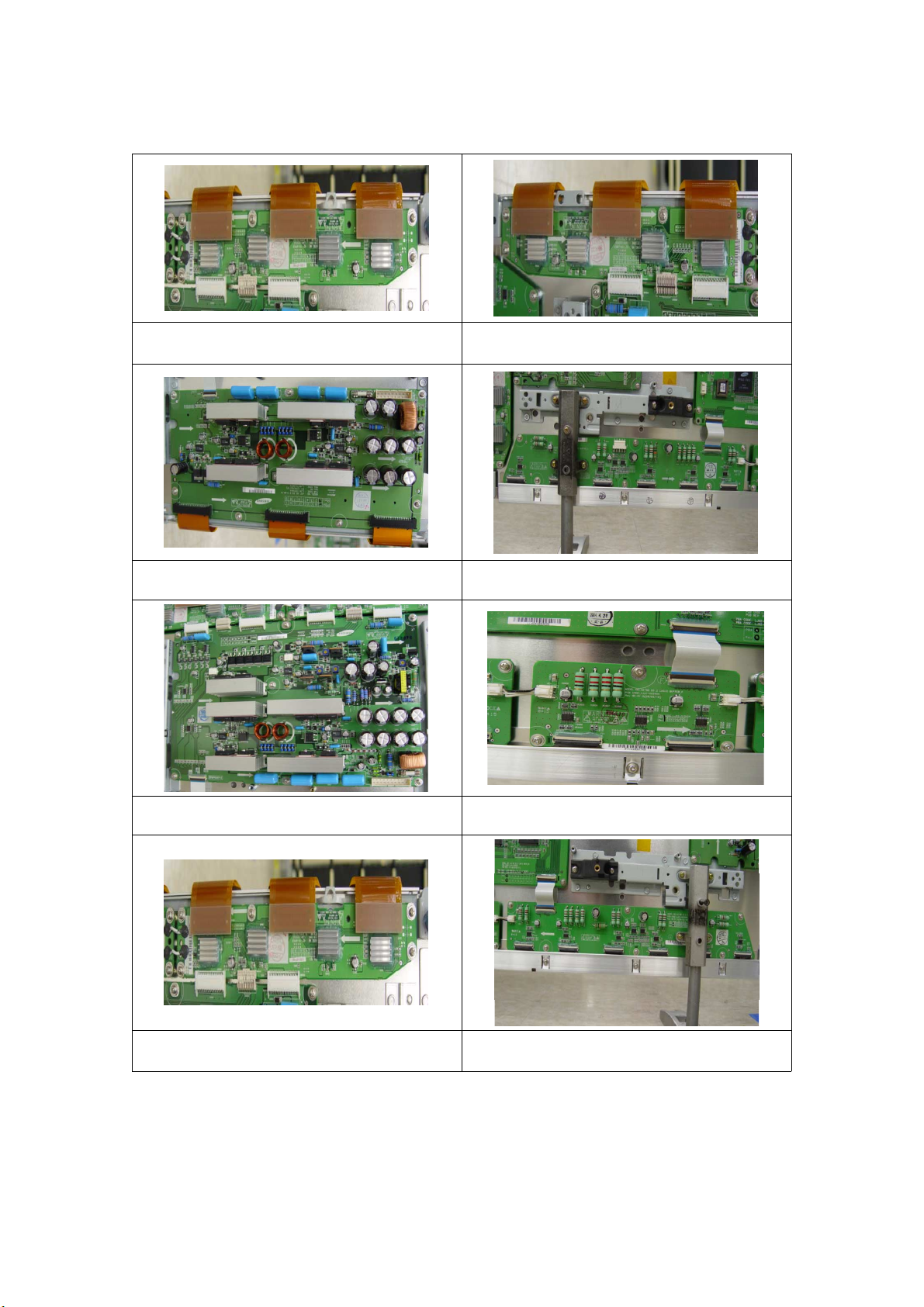
5. DISASSEMBLING/REASSEMBLING ···················································································· 31
5-1. Tools/Measurements··············································································································· 31
5-2. Exploded View························································································································· 31
5-3. Removal Procedures··············································································································· 32
5-3-1. Removing the Logic PCB Ass'y board from the Chassis Base······································ 32
5-3-2. Removing the Y-Main Ass'y board from the Chassis Base············································ 32
5-3-3. Removing the X-Main Ass'y board from the Chassis Base············································ 32
5-3-4. Removing the Y-BUFFER board from the Chassis Base ·············································· 33
5-3-5. Removing the ADDRESS-BUFFER board from the Chassis Base································ 33
5-4. Installation Procedures············································································································ 34
5-4-1. Installing the TCPs on the Logic Buffer ········································································· 34
5-4-2. Installing the Y-Main Ass'y Board on the Y-Buffer························································· 35
5-4-3. Installing X-Main and Y-Main Ass'y boards on the Chassis Base·································· 35
5-4-4. Installing the Logic PCB Ass'y board on the Chassis Base ··········································· 36
- 1 -

6. Operation Checks After Repair Service·············································································· 38
6-1. Check Items ···························································································································· 38
6-2. Check Procedure····················································································································· 38
7. Adjustment Procedure ········································································································· 39
7-1 Adjustment Spec. and locations ································································································· 39
7-2. Procedure·································································································································· 39
8. DATA······································································································································ 43
• Back Side (TCP type) ···················································································································· 43
• Logic Main Block Diagram ············································································································· 44
• Drive Waveform ····························································································································· 45
• Reset ············································································································································· 46
• Address (Scan) ······························································································································ 47
• Sustain Waveform ························································································································· 48
9. Service Parts ························································································································· 49
- 2 -
1. OUTLINE
1-1. Model Name of Plasma Display
MODEL : S42SD-YB03
1-2. External View
< M1 = X Board + Y Board + Logic Board >
- 3 -
1-3. Specifications
No
1
2
3
4
5
6
7
8
9
Item
Pixel
Number of Cells
Pixel pitch 1095 (H) x 1110 (V) mm
Cell Pitch
Display size
Screen size Diagonal 42" Color Plasma Display Module
Screen aspect 16 : 9
Display color 16.77 million colors
Viewing angle
R 0.365 (H) x 1.110 (V) mm
G 0.365 (H) x 1.110 (V) mm
B 0.365 (H) x 1.110 (V) mm
(Angle with 50% and greater brightness perpendicular to PDP module.)
852 (H) x 480 (V) pixels (1 pixel = 1 R, G, B cells)
932.940 (H) x 532.800 (V) mm
Specification
2556 (H) x 480 (V)
[36.73 x 20.98 inches]
Over 160º
10
11
12
13
Broadcasting reception vertical
14
Dimensions 982 (W) x 582 (H) x 52.9 (D) mm
Weight Module 1 About 16.6 kg
Packing weight Module 1 240 ± 5kg (including modules) / 10pcs/BOX
Packing size L1175 x W1140 x H970 (mm)/10pcs / BOX
frequency
and
video/logic interface
S42SD-YB03 60Hz/50Hz, LVDS
- 4 -

2. PRECAUTIONS
To prevent the risks of unit damage, electrical shock and radiation, take the following safety, service, and ESD
precautions.
2-1. Handling Precautions for Plasma Display
2-2. Safety Precautions for Service (Handling, prevention of electrical shock, measure
against power outage, etc)
2-2-1. Safety Precautions
1) Before replacing a board, discharge forcibly the remaining electricity from the board.
2) When connecting FFC and TCPs to the module, recheck that they are securely
connected.
3) To prevent electrical shock, be careful not to touch leads during circuit operations.
4) To prevent the Logic circuit from being damaged, do not connect/disconnect signal
cables during circuit operations.
5) Follow voltage information when adjust it.
6) Before reinstalling the chassis and the chassis assembly, be sure to use necessary
protective stuffs.
7) Caution for design change: Do not install any additional devices to the module, and do
not change the electrical circuit design.
8) If any parts or wire is overheated or damaged, replace it with a new specified one
immediately, and identify the cause of the problem to resolve it.
- 5 -

9) Check that the wires are correctly arranged and connected. Do not change the
distances between the parts and the printed circuit board. Check that the AC power
cord is not damaged. Keep heating parts away from lead wires and other parts.
10) Product safety indication : Some electrical circuits and devices have specific safety
characteristics. Therefore when replacing parts, use the same parts as originals.
Safety and protective function will be lost even if parts with higher voltage and wattage
capability are used.
11) Be sure to disconnect the AC power cord before servicing.
12) After servicing, check that the screws, parts, and wires are correctly installed. Also
check that the peripheral parts are not damaged.
2-2-2. Precautions for servicing electrostatic sensitive devices
Some semiconductors (such as ICs and FETs) are easily damaged by electrostatic.
These devices are called electrostatic sensitive devices (ESD).
The rate of electrostatic damage to devices can be decreased by observing the
following precautions.
1) Before handling semiconductors and assemblies, discharge electrostatic from your
body with an earth ground, or wear an antistatic band.
(Be sure to discharge electrostatic before turning on the power, to prevent electrical
shock)
2) After removing the ESD assembly, place it on an antistatic mat with aluminum foil to
avoid electrostatic charge.
3) Use only a ground-tip soldering iron to solder and unsolder the ESD.
4) Use only an antistatic soldering removal device for the ESD. General soldering
removal devices are non-antistatic. Using such non-antistatic devices will damage the
ESD.
- 6 -

5) Before removing the protective material from the lead of a new ESD, bring the lead
into contact with the chassis or the circuit assembly that the ESD is to be installed on.
6) When handling an unpacked ESD for replacement, do not move around too much.
Moving (legs on the carpet, for example) generates enough electrostatic to damage
the ESD.
7) Do not take a new ESD from the protective case until the ESD is ready to be installed.
Most ESDs have a lead, which is easily short-circuited by conductive materials (such
as conductive foam and aluminum).
- 7 -
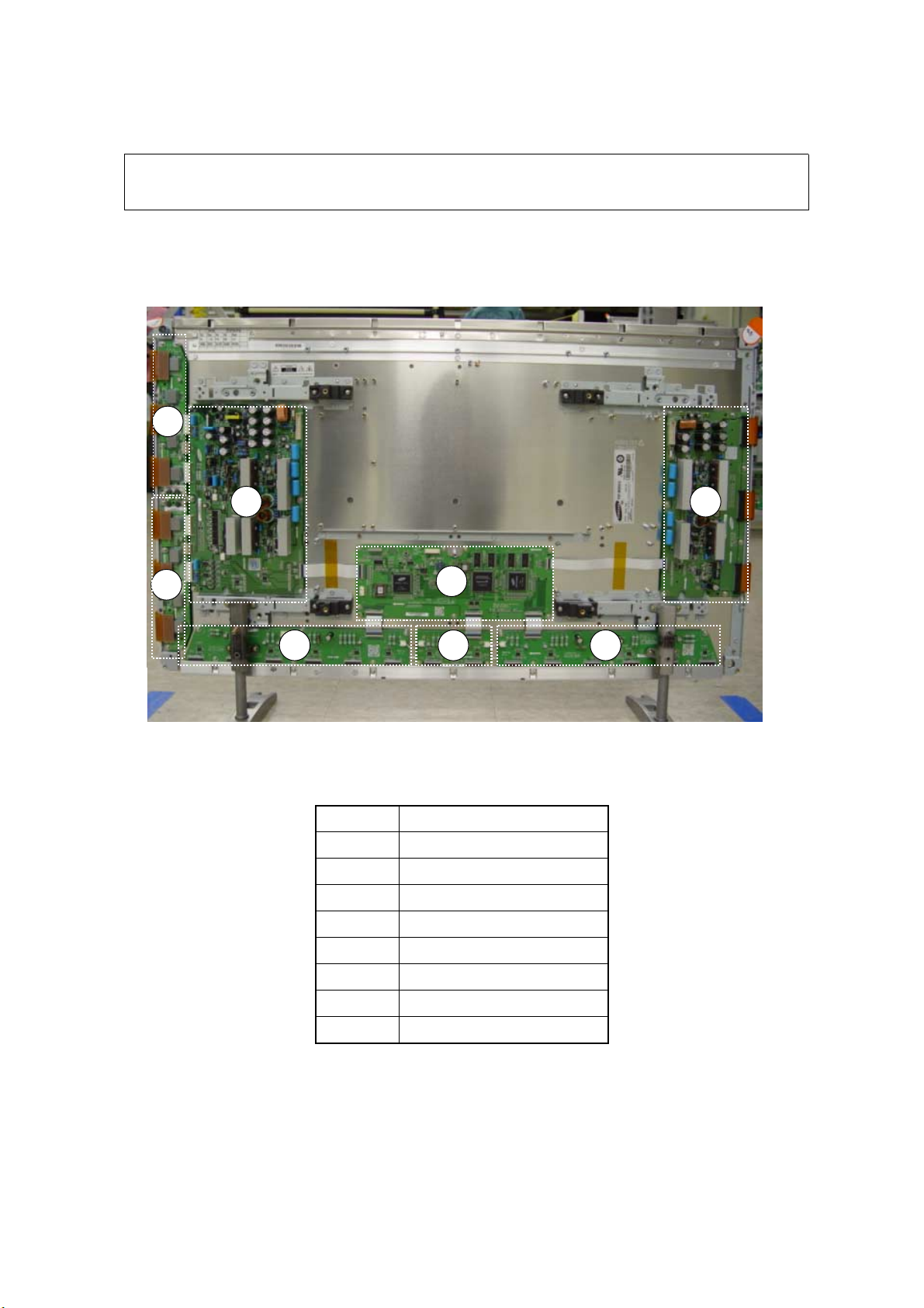
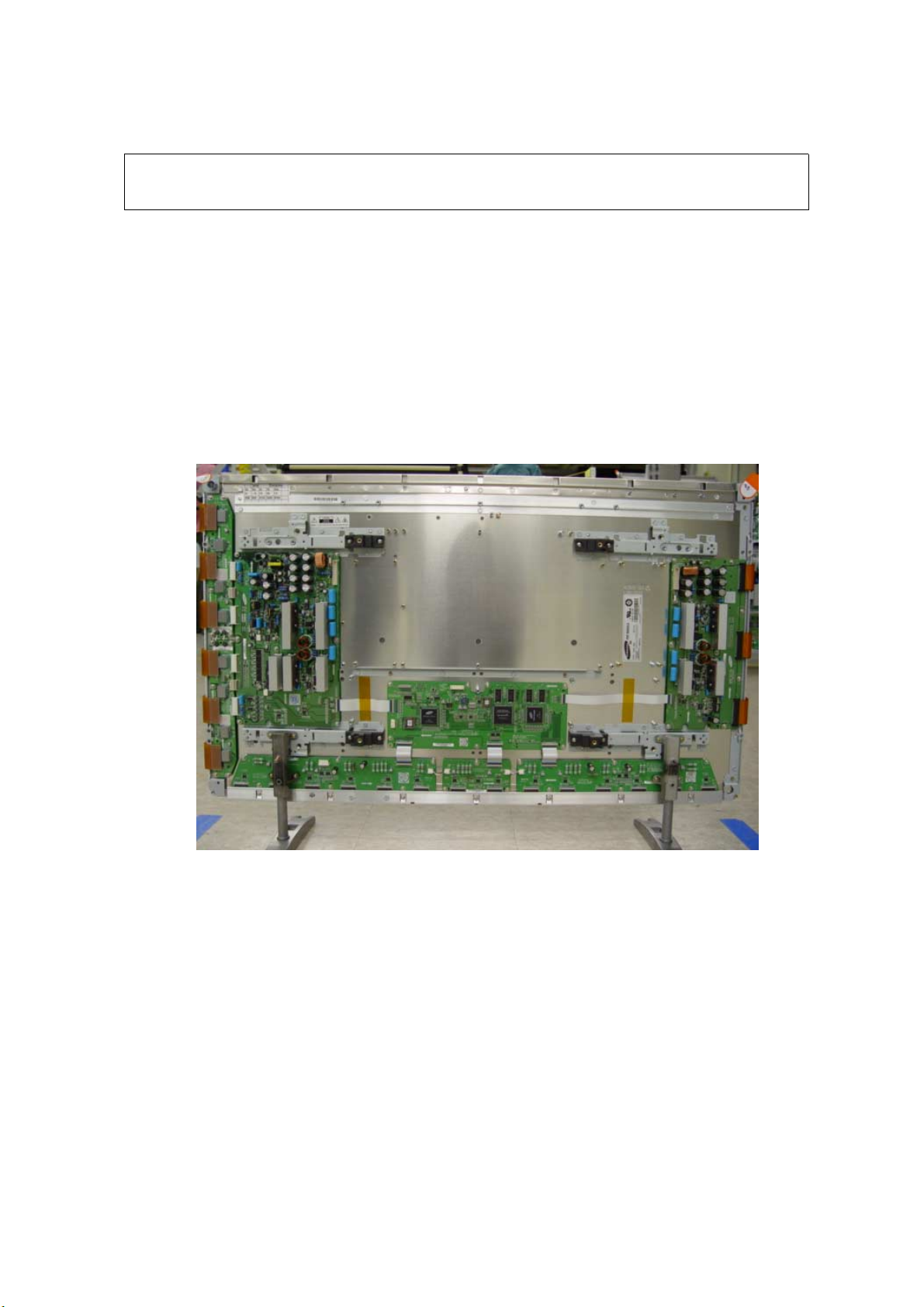
3. NAME and FUNCTION
3-1. Layout of Assemblies
4
5
6 7 8
2 3
1
No. Board
1 Logic Main
2 X-Main
3 Y-Main
4 Y-Buffer (upper)
5 Y-Buffer (lower)
6 Logic E Buffer
7 Logic F Buffer
8 Logic G Buffer
- 8 -
1. L-Main 5. Y-Buffer (lower)
2. X-Main 6. E-Buffer
3. Y-Main 7. F-Buffer
4, Y-Buffer (upper) 8. G-Buffer
- 9 -
3-2. Block Diagrams
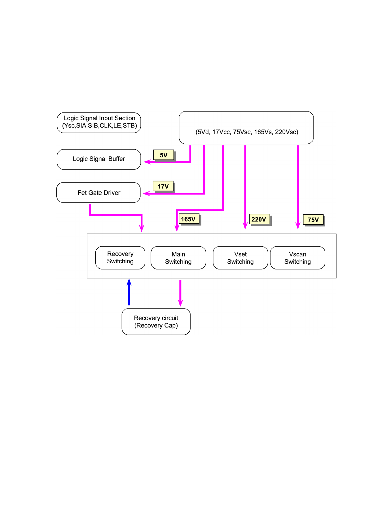
3-2-1. Block Diagrams for Drive Circuit Operations
<Drive Y Board>
- 10 -
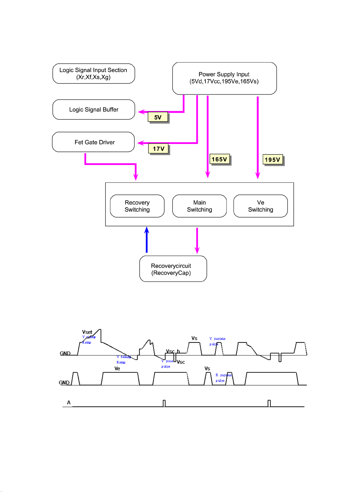
<Drive X Board>
<Drive Waveforms>
- 11 -
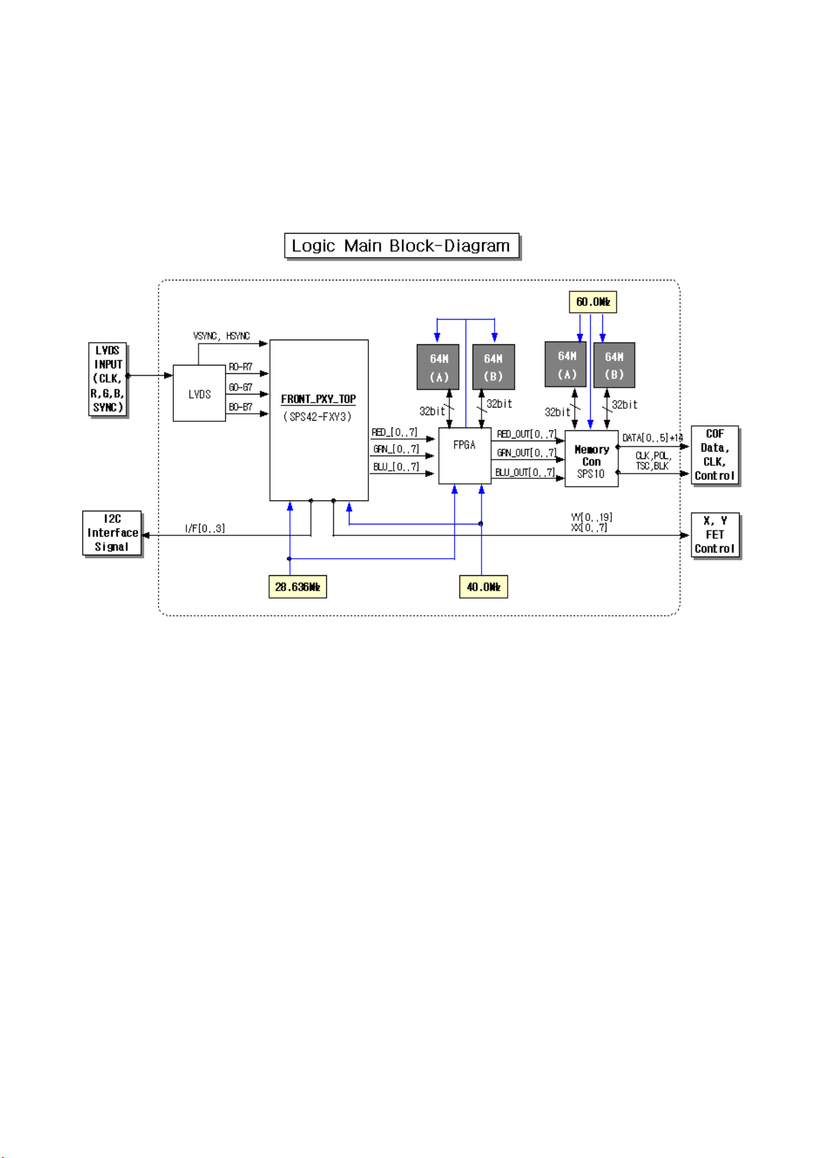
3-2-2. Logic Circuit Block Diagram
3-3. Main Functions of Each Assembly
3-3-1. X-Main board
The X-MAIN board generates a drive signal by switching the FET in synchronization
with the Logic Main board timing, and supplies the X electrode of the panel with the
drive signal through the connector. This board, connected to the panel’s X terminal,
has the following main functions.
1) Maintain voltage waveforms (including ERC).
2) Generate X Rising Ramp signal.
3) Maintain Ve bias between scan intervals.
- 12 -

3-3-2. Y-Main board
The Y-MAIN board generates a drive signal by switching the FET in synchronization
with the Logic Main board timing, and sequentially supplies the Y electrode of the
panel with the drive signal through the scan driver IC on the Y-buffer board. This
board, connected to the panel’s Y terminal, has the following main functions:
1) Maintain voltage waveforms (including ERC).
2) Generate Y Rising Ramp signal.
3) Maintain Vscan bias.
3-3-3. Logic Main board
The Logic Main board generates and outputs the address drive output signal and the
XY drive signal by processing the video signals. This board buffers the address drive
output signal and feeds it to the address driver IC (COF module).
(Video signal processing – XY drive signal generation - frame memory control –
address/data rearrangement – system control)
3-3-4. Logic buffer (E, F)
The logic buffer transmits data signals and control signals using a COF (Chip on
Flexible).
3-3-5. Y-buffer board (upper/lower)
The Y-buffer board consisting of the upper and lower boards supplies the Y terminal
with a scan waveform. The board comprises eight scan driver ICs (STMicroelectronics
STV7617: 64 or 65 output pins), but four ICs for the SD Class.
3-3-6. COF (Chip on Flexible)
The COF applies Va pulse to the address electrode, and constitutes address
discharge by the potential difference between the Va pulse and the pulse applied to
the Y electrode. The COF comprises four data driver ICs (STV7610A: 96 output pins).
Seven COFs are required for single scan.
- 13 -
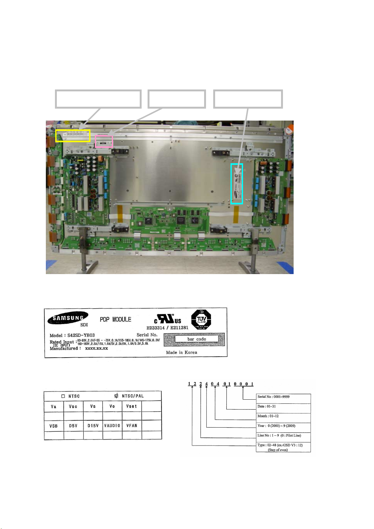
3-4. Product/Serial Label Locations
Voltage information label Serial No. label Panel module label
Panel Module Label
Voltage information Label Serial No. Label
(Voltage specification)
- 14 -
4. OPERATION CHECKING AFTER RECTIFICATION
4-1. Flow Charts
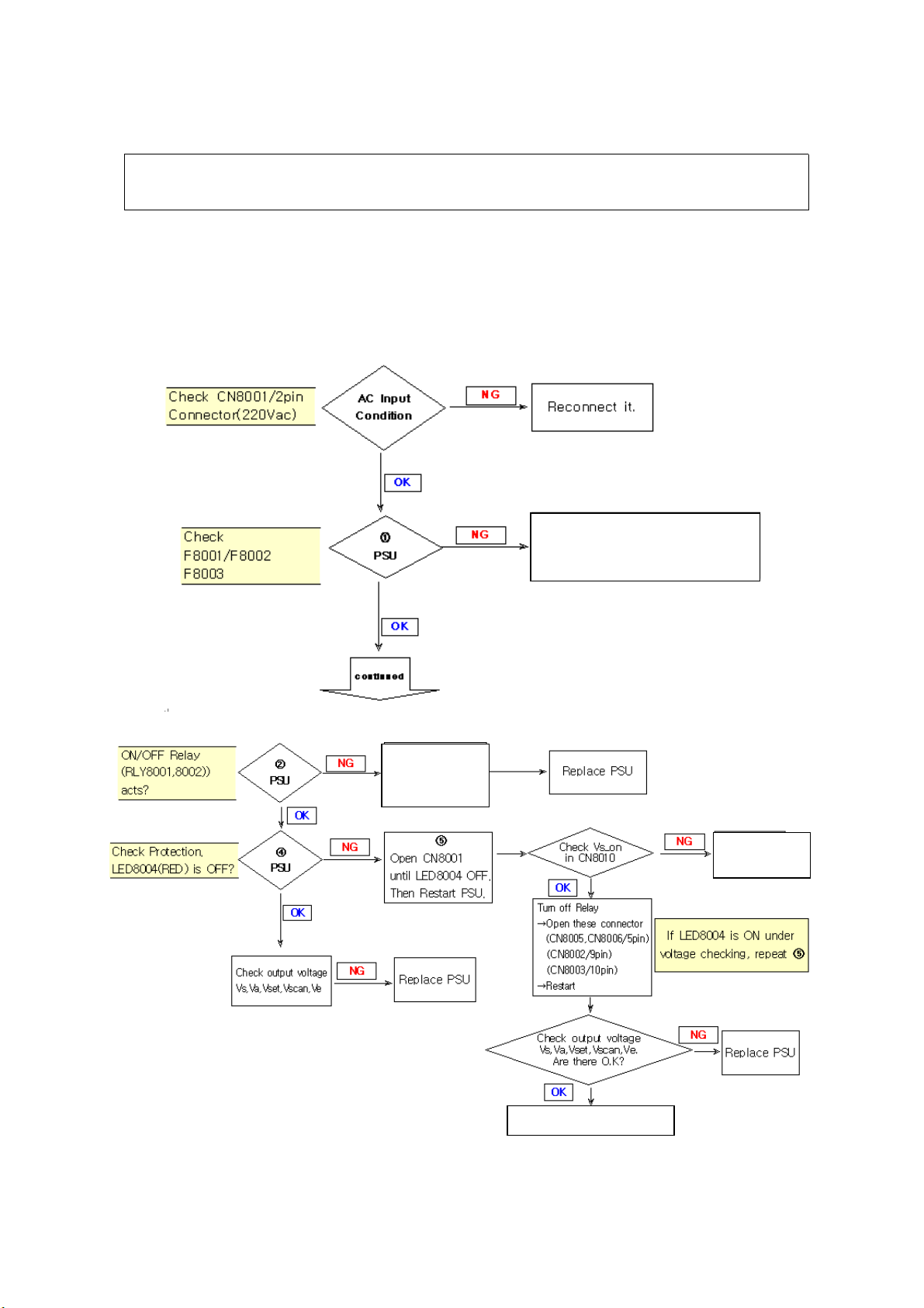
4-1-1. No voltage output
Replace PSU and
check driver B’D in advance
(Refer to ‘4-1-2 No display’)
LED (Green)
RLY8001,8002
off
Go to ‘4-1-2 No Display’
Go to ‘4-1-2
No Display’
- 15 -
 Loading...