

Page 1
MODIFICATION HISTORY
MODEL NAME : KDX-46Q005
SERVICE MANUAL
PA RTS No. : 9-878-325-03
* Blue characters are linking.
Ver. DATA CONTENTS
1.0 2005. 9 Issued
1.1 2005. 12 Addition of REPAIR MANUAL for Centralized Service Center (APPENDIX)
1.2 2006. 2 4. EXPLODED VIEWS. Part numbers changed (No. 6, 105, 155)
Part added (No. 265)
Part deleted (No. 358)
APPENDIX ELECTRICAL PARTS LIST
Parts deleted (DE6 Board IC5910, PD Board IC9507, T1MJ Board IC9019)
Page 2
KDX-46Q005
SERVICE MANUAL
XDM-F4600QMBD-Q005
US Model
Canadian Model
MR3 CHASSIS
SPECIFICATIONS
Panel System LCD Panel
Display Resolution 1920 pixels (horizontal) x 1080 pixels (vertical)
Antenna 75 ohm external terminal for VHF/UHF
Television System NTSC American TV Standard
ATSC (8VSB terrestrial) ATSC compliant 8VSB
QAM on cable ANSI/SCTE 07 2000
Screen Size (measured diagonally) 46 inches
Channel Coverage Terrestrial (analog) 2-69
Cable TV (analog) 1-125
Terrestrial (digital) 2-69
Cable TV (digital) 1-135
Power Requirements 120V, 60 Hz
Inputs/Outputs
HDMI IN 2 total Video: 1080i, 720p, 480p, 480i
Audio: Two channel linear PCM 32, 44.1 and
48 kHz, 16, 20 and 24 bit
✍
Not compatible with compressed sound,
such as AC-3 and DTS.
Video (IN) 3 total (1 on front unit) 1 Vp-p, 75 ohms unbalanced, sync negative
S Video (IN) 3 total (1 on front unit) Y: 1 Vp-p, 75 ohms unbalanced, sync negative
C: 0.286 Vp-p (Burst signal), 75 ohms
Audio (IN) 6 total (1 on front unit) 500 mVrms (100% modulation)
Impedance: 47 kilohms
LCD DIGITAL COLOR TV
Page 3

Component Video Input 2 (YPBPR)
Y: 1.0 Vp-p, 75 ohms unbalanced, sync
negative
P
B: 0.7 Vp-p, 75 ohms
P
R: 0.7 Vp-p, 75 ohms
CONTROL S (IN) 1
CONTROL S (OUT) Mini jack
1
Mini jack
AUDIO (VAR/FIX) OUT 1 500 mVrms at the maximum volume setting
(Variable)
500 mVrms (Fixed)
Impedance (output): 2 kilohms
i.LINK 3 total (1 on front panel) 4-pin S400 i.LINK terminal
RF Inputs 2
Digital Audio Optical Output
1 Optical Rectangular (1)
(PCM/Dolby Digital)
CableCARD Slot PCMCIA Type I/II
SUBWOOFER (VAR)(OUT) 1
CENTER SPEAKER (IN) Max. 180 W (6Ω), 1 kHz, Sensitivity 30 Vp-p
1
Phono jack
1
DISPLAY SIGNAL OUT 1 Black
1 White
PC (IN) 1 (D-sub 15pin)
PC AUDIO (IN) 1 Stereo mini jack, 500 mVrms, 47 kilohms
Speaker Output 25 W (L), 25 W (R), 50 W (Woofer)
Dimensions (W × H × D) Display 1239 x 717 x 130 (mm)
Media Receiver Unit 430 x 97 x 350 (mm)
Mass Display Approx. 59 kg Media Receiver Unit Approx. 9.1 kg
Power Consumption
In Use Display 612 W
Media Receiver Unit 60 W
In Standby Display 0.5 W
Media Receiver Unit 0.4 W
In i.LINK/CableCARD Standby Less than 30 W
Supplied Accessories
Remote Control RM-Y1000
AA (R6) Batteries 2 supplied for remote control
AC Power Cord 2
AC Plug Holder 1
Display Interface Cable
1
Antenna Cable 1
Vertical Installation Stand 1
Vertical Installation Stand Screws 2
Owner’s Guide 1
Quick Setup Guide 1
Warranty 1
Product Registration Card 1
Design and specifications are subject to change without notice.
KDX-46Q005 (UC) 2
Page 4

WARNINGS AND CAUTIONS
A
A
CAUTION
These servicing instructions are for use by qualified service personnel only To reduce the risk of electric shock, do not perform any
servicing other than that contained in the operating instructions unless you are qualified to do so.
WARNING!!
n isolation transformer should be used during any service to avoid possible shock hazard, because of live chassis. The chassis of
this receiver is directly connected to the ac power line.
!
SAFETY-RELATED COMPONENT WARNING!!
Components identified by shading and ! mark on the schematic diagrams, exploded views, and in the parts list are critical for safe
operation. Replace these components with Sony parts whose part numbers appear as shown in this manual or in supplements
published by Sony. Circuit adjustments that are critical for safe operation are identified in this manual. Follow these procedures
whenever critical components are replaced or improper operation is suspected.
ATTENTION!!
Ces instructions de service sont à l’usage du personnel de service qualifié seulement. Pour prévenir le risque de choc électrique, ne
pas faire l’entretien autre que celui contenu dans le Mode d’emploi à moins que vous soyez qualifié faire ainsi.
fin d’eviter tout risque d’electrocution provenant d’un chássis sous tension, un transformateur d’isolement doit etre utilisé lors de tout
dépannage. Le chássis de ce récepteur est directement raccordé à l’alimentation du secteur
!
ATTENTION AUX COMPOSANTS RELATIFS A LA SECURITE!!
Les composants identifies par une trame et par une marque ! sur les schemas de principe, les vues explosees et les listes de pieces
sont d’une importance critique pour la securite du fonctionnement. Ne les remplacer que par des composants Sony dont le numero
de piece est indique dans le present manuel ou dans des supplements publies par Sony. Les reglages de circuit dont l’importance
est critique pour la securite du fonctionnement sont identifies dans le present manuel. Suivre ces procedures lors de chaque
remplacement de composants critiques, ou lorsqu’un mauvais fonctionnement suspecte.
KDX-46Q005 (UC) 3
Page 5
SAFETY CHECK-OUT
After correcting the original service problem, perform the
following safety checks before releasing the set to the customer:
1. Check the area of your repair for unsoldered or poorly-soldered connections. Check the entire board surface for solder
splashes and bridges.
2. Check the interboard wiring to ensure that no wires are
“pinched” or contact high-wattage resistors.
3. Check that all control knobs, shields, covers, ground straps,
and mounting hardware have been replaced. Be absolutely certain that you have replaced all the insulators.
4. Look for unauthorized replacement parts, particularly transistors, that were installed during a previous repair. Point them
out to the customer and recommend their replacement.
5. Look for parts which, though functioning, show obvious signs
of deterioration. Point them out to the customer and recommend their replacement.
6. Check the line cords for cracks and abrasion. Recommend the
replacement of any such line cord to the customer.
7. Check the antenna terminals, metal trim, “metallized” knobs,
screws, and all other exposed metal parts for AC Leakage.
Check leakage as described right.
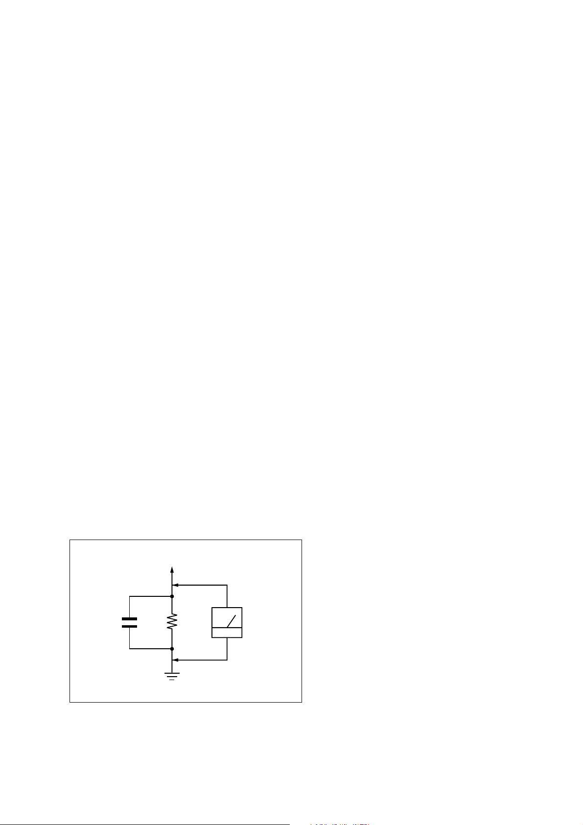
LEAKAGE TEST
The AC leakage from any exposed metal part to earth ground and
from all exposed metal parts to any exposed metal part having a
return to chassis, must not exceed 0.5 mA (500 microamperes).
Leakage current can be measured by any one of three methods.
1. A commercial leakage tester, such as the Simpson 229 or RCA
WT-540A. Follow the manufacturers’ instructions to use these
instruments.
2. A battery-operated AC milliammeter. The Data Precision 245
digital multimeter is suitable for this job.
3. Measuring the voltage drop across a resistor by means of a
VOM or battery-operated AC voltmeter. The “limit” indication is 0.75 V, so analog meters must have an accurate lowvoltage scale. The Simpson 250 and Sanwa SH-63Trd are examples of a passive VOMs that are suitable. Nearly all battery
operated digital multimeters that have a 2 V AC range are suitable. (See Fig. A)
WARNING!!
SAFETY-RELATED COMPONENT WARNING!!
COMPONENTS IDENTIFIED BY SHADING AND MARK !
ON THE SCHEMATIC DIAGRAMS, EXPLODED VIEWS
AND IN THE PARTS LIST ARE CRITICAL FOR SAFE
OPERATION. REPLACE THESE COMPONENTS WITH
SONY PARTS WHOSE PART NUMBERS APPEAR AS
SHOWN IN THIS MANUAL OR IN SUPPLEMENTS PUBLISHED BY SONY. CIRCUIT ADJUSTMENTS THAT ARE
CRITICAL FOR SAFE OPERATION ARE IDENTIFIED IN
THIS MANUAL. FOLLOW THESE PROCEDURES WHENEVER CRITICAL COMPONENTS ARE REPLACED OR
IMPROPER OPERATION IS SUSPECTED.
AVERTISSEMENT!!
ATTENTION AUX COMPOSANTS RELATIFS À LA
SÉCURITÉ!!
LES COMPOSANTS IDENTIFIÉS PAR UNE TRAME ET
UNE MARQUE ! SONT CRITIQUES POUR LA
SÉCURITÉ. NE LES REMPLACER QUE PAR UNE
PIÈCE PORTANT LE NUMÉRO SPECIFIÉ. LES
RÉGLAGES DE CIRCUIT DONT L’IMPORTANCE EST
CRITIQUE POUR LA SÉCURITÉ DU
FONCTIONNEMENT SONT IDENTIFIÉS DANS LE
PRÉSENT MANUEL. SUIVRE CES PROCÉDURES
LORS DE CHAQUE REMPLACEMENT DE
COMPOSANTS CRITIQUES, OU LORSQU’UN MAUVAIS
FONCTIONNEMENT EST SUSPECTÉ.
To Exposed Metal
Parts on Set
0.15 µF
1.5 k
Ω
Earth Ground
AC
Voltmeter
(0.75 V)
Fig. A. Using an AC voltmeter to check AC leakage.
KDX-46Q005 (UC) 4
Page 6

TABLE OF CONTENTS
1. SELF DIAGNOSIS FUNCTION
1-1. SUMMARY OF SELF-DIAGNOSIS
FUNCTION ........................................................ 1-1
1-2. DIAGNOSIS ITEMS AND PREDICTION OF
MALFUNCTION LOCATION ......................... 1-1
2. DISASSEMBLY
2-1. DISPLAY UNIT (XDM-F4600Q) ..................... 2-1
2-1-1. REAR FRAME ASSY AND REAR
HEATSINK ASSY REMOVAL ................... 2-1
2-1-2. SPEAKER REMOVAL ................................. 2-1
2-1-3. K BOARD REMOVAL ................................. 2-2
2-1-4. G1B AND G2L BOARDS REMOVAL ........ 2-2
2-1-5. F BOARD REMOVAL .................................. 2-3
2-1-6. DE6 BOARD REMOVAL ............................ 2-3
2-1-7. LCD PANEL REMOVAL ............................. 2-4
2-1-8. H1D BOARD REMOVAL ............................ 2-5
2-1-9. H2D BOARD REMOVAL ............................ 2-5
2-2. MEDIA RECEIVER UNIT (MBD-Q005) ........ 2-6
2-2-1. TOP AND SIDE PANEL REMOVAL ......... 2-6
2-2-2. REAR PANEL BLOCK ASSY AND FAN
BLOCK ASSY REMOVAL .......................... 2-6
2-2-3. CSMU BOARD REMOVAL ........................ 2-7
2-2-4. QI, QMDV AND QT BOARDS
REMOVAL .................................................... 2-8
2-2-5. DDM BLOCK ASSY AND J1MU BOARD
REMOVAL .................................................... 2-9
2-2-6. DIC3, M1MU AND T1MJ BOARDS
REMOVAL .................................................... 2-10
2-2-7. A1MU, PD AND QUMU BOARDS
REMOVAL .................................................... 2-10
2-2-8. FRONT BLOCK ASSY AND G1MU BOARD
REMOVAL .................................................... 2-11
2-2-9. H1MU BOARD REMOVAL ........................ 2-11
2-2-10. QH BOARD REMOVAL .............................. 2-12
3. DIAGRAMS
3-1. CIRCUIT BOARDS LOCATION ..................... 3-1
3-1-1. DISPLAY UNIT (XDM-F4600Q) ................ 3-1
3-1-2. MEDIA RECEIVER UNIT (MBD-Q005) .... 3-1
3-2. BLOCK DIAGRAMS ........................................ 3-2
3-2-1. DISPLAY UNIT (XDM-F4600Q) ................ 3-2
(1) DE6, H1D and H2D Boards .......................... 3-2
(2) K Board .......................................................... 3-3
(3) F and G1B Boards.......................................... 3-4
(4) G2L Board...................................................... 3-5
3-2-2. MEDIA RECEIVER UNIT (MBD-Q005) .... 3-6
(1) A1MU(1/2), CSMU and H1MU(1/2) Boards 3-6
(2) A1MU(2/2) Board.......................................... 3-7
(3) J1MU Board ................................................... 3-8
(4) DIC3 Board .................................................... 3-9
(5) T1MJ Board ................................................... 3-10
(6) M1MU and H1MJ(2/2) Boards ..................... 3-11
(7) PD Board ........................................................ 3-12
(8) QI Board......................................................... 3-13
(9) QH and QMDV (1/2) Boards ........................ 3-14
(10) QMDV (2/2) Board ........................................ 3-15
(11) QT and QUMU Boards .................................. 3-16
(12) G1MU Board ..................................................3-17
3-3. FRAME DIAGRAMS ........................................ 3-18
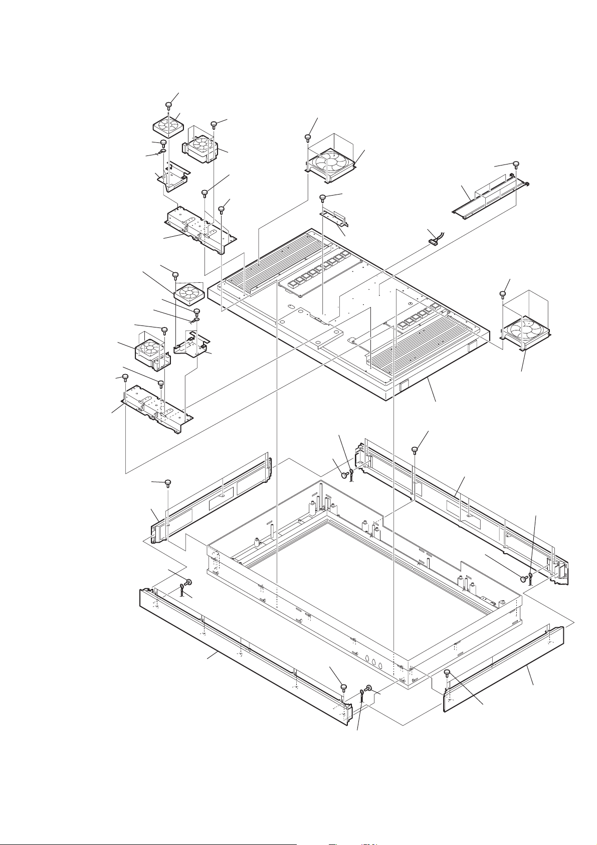
4. EXPLODED VIEWS
4-1. DISPLAY UNIT (XDM-F4600Q) ..................... 4-2
4-1-1. REAR FRAME ASSY AND REAR
HEATSINK ASSY ........................................ 4-2
4-1-2. CHASSIS-1 .................................................... 4-3
4-1-3. CHASSIS-2 .................................................... 4-4
4-1-4. BEZEL ASSY AND LCD PANEL ............... 4-5
4-2. MEDIA RECEIVER UNIT (MBD-Q005) ........ 4-6
4-2-1. PANEL AND COVER .................................. 4-6
4-2-2. CHASSIS-1 .................................................... 4-7
4-2-3. CHASSIS-2 .................................................... 4-8
4-2-4. CHASSIS-3 .................................................... 4-9
4-2-5. CHASSIS-4 .................................................... 4-10
4-2-6. FRONT PANEL ASSY ................................. 4-11
4-3. PACKING MATERIALS .................................. 4-12
4-3-1. MEDIA RECEIVER UNIT ........................... 4-12
4-3-2. DISPLAY UNIT AND MEDIA
RECEIVER UNIT .......................................... 4-13
KDX-46Q005 (UC) 5
Page 7
SECTION 1
SELF DIAGNOSIS FUNCTION
1-1. SUMMARY OF SELF-DIAGNOSIS FUNCTION
1. This device includes a self-diagnosis function.
2. In case of abnormalities, the POWER/STANDBY indicator automatically blinks.
It is possible to predict the abnormality location by the number of blinks.
The instruction manual describes blinking of the POWER/STANDBY indicator.
3. If the symptom is not reproduced sometimes in case of a malfunction, there is recording of whether a malfunction was generated or
not.
Operate the remote command to confirm the matter on the screen and to predict the location of the abnormality.
1-2. DIAGNOSIS ITEMS AND PREDICTION OF MALFUNCTION LOCATION
1. When a malfunction occurs the POWER/STANDBY indicator only blinks for one of the following diagnosis items.
In case of two or more malfunctions, the item which first occurred blinks.
If the malfunctions occurred simultaneously, the item with the lower blink count blinks first.
2. The screen display displays the results regarding all the diagnosis items listed below.
•RECEIVER UNIT (MBD-Q005)
Number of
Diagnosis item
BOX TEMP
+B OVP
FAN
LOWB ERR
D OVP
PNL ERR
LED (POWER/STANDBY)
blink times
2 times
3 times
4 times
6 times
8 times
9 times
Possible cause (faulty location)
Excessively high ambient temperature or overheat of BOX (due to dust, etc.).
Improper connection of inter-board connectors.
Fan (or fan stop due to dust or other causes).
• Main converter primary circuit.
• Secondary-side regulator circuit.
• PFC converter circuit.
• AC-RLY circuit, AC-RYL signal line.
• STBY circuit.
• THRU3.3V circuit.
• THRU3.3V, SW_5V, SW_3.3V, SW_2.5V line output (over voltage).
Panel unit.
KDX-46Q005 (UC) 1-1
Page 8
•DISPLAY UNIT (XDM-F4600Q)
Diagnosis item
LED POWER ERR
FAN P-TEMP
POWER (G_PROT)
AU PROT
LED ERR
POWER ERR (PS_PROT)
Number of
LED(POWER ON/STANDBY)
blink times
Green/red alternate blinking
4 times
6 times
7 times
9 times
11 times
FAN
HARNESS
BL (LED)
FAN
LCD
Possible cause (faulty location)
Failure part etc.
• Main converter primary circuit, F/B circuit,
rectifier diodes.
• SUB11V circuit.
• Fan (or fan stop due to dust or other causes).
• Disconnection of fan relay connector,
short-circuit/disconnection due to cable catching.
• Fan drive circuit.
• Excessively high ambient temperature or overheat
of Panel unit (due to dust, etc.)
• SUB6.5V/P_VCC circuit.
• 3.3V, 1.8V (generated from SUB6.5V).
• Speaker output DC (over 2VDC).
• Audio_VCC short-circuit.
• Sub_11V short-circuit
• LED backlight microcomputer communication
error ("No Ack" continues for a predetermined time).
• LED_ERROR: LEDs/arrays in BL (open).
• TEMP_ERROR: LED backlight overheat.
• TEMP SENSOR_ERROR: Boards, I2C bus, harness
disconnection (including communication error)
• PHOTO SENSOR_ERROR: Boards, interface bus,
harness disconnection
(including communication error).
• FAN_ERROR: Fan, fan drive circuit, harness
disconnection
• P_VCC circuit.
• P_VCC (LCD panel power) short-circuit in
T-CON board of LCD.
KDX-46Q005 (UC) 1-2E
Page 9
SECTION 2
DISASSEMBLY
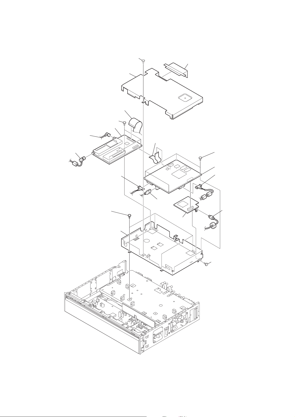
2-1. DISPLAY UNIT (XDM-F4600Q)
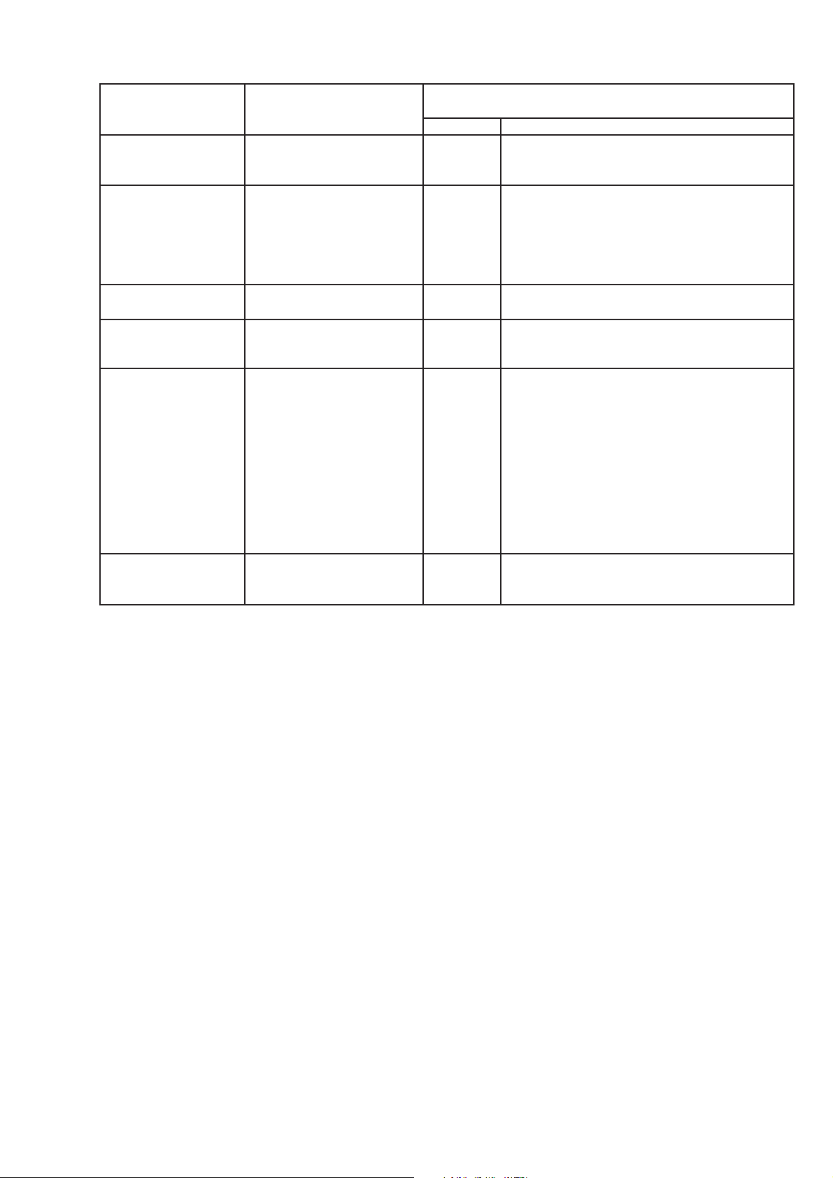
2-1-1. REAR FRAME ASSY AND REAR HEATSINK ASSY REMOVAL
2 Four screws
(+FLAT HEAD (M4 GRIP) )
1 Four screws
(+FLAT HEAD TP 4x12)
5 Four screws
(+FLAT HEAD (M4 GRIP) )
7 Four screws
(+FLAT HEAD (M4 GRIP) )
3 Rear frame assy (L)
7 Four screws
(+FLAT HEAD (M4 GRIP) )
4 Four screws
(+FLAT HEAD TP 4x12)
6 Rear frame assy (R)
7 Four screws
(+FLAT HEAD (M4 GRIP) )
8 Rear heatsink assy
2-1-2. SPEAKER REMOVAL
4 Speaker (L)
3 Four screws
(+PWH 4x16)
1 Four screws
(+PWH 4x16)
2 Speaker (R)
KDX-46Q005 (UC) 2-1
Page 10
2-1-3. K BOARD REMOVAL
2 Four screws
(+PSW 4x10)
1 Two screws
(+PSW 4x10)
4 Two screws
(+PSW 3x6)
6 Two screws
(+PSW 3x6)
8 Top shield (K)
7 K board
5 One screw
(+PSW 4x8)
3 Stay support assy
2-1-4. G1B AND G2L BOARDS REMOVAL
9 Three screws
(+PSW 3x10)
0 Bottom shield (K)
1 Six screws
(+PSW 3x6)
2 G1B board
3 Four screws
(+PSW 3x6)
4 G2L board
KDX-46Q005 (UC) 2-2
Page 11
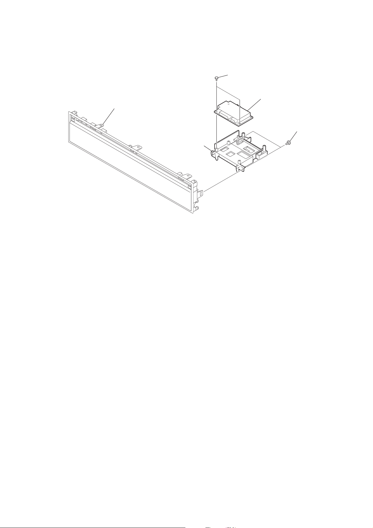
2-1-5. F BOARD REMOVAL
1 Four screws
(+PSW 3x6)
2 F board
6 Five screws
(+PSW 3x6)
7 Chassis bracket
4 One screw
(+PSW 4x8)
3 Four screws
(+PSW 4x8)
5 Connector shield
2-1-6. DE6 BOARD REMOVAL
1 Two screws
2 Two screws
(M2.6 S-HEAD EG GRIP)
3 Three screws
(+PSW 3x6)
7 Four screws
(+PSW 3x6)
8 Bottom shield (DE)
(HEX)
4 Top shield (DE)
5 Four screws
(+PSW 3x6)
6 DE6 board
wd Six screws
(+PSW 4x10)
qd Two screws
(+PSW 3x20)
qf Dc fan
qg Two screws
(+PSW 4x10)
qh Earth lead
qj Fan bracket (A)
9 Four screws
(+PSW 4x8)
0 Stand holder
qa Four screws
(+PSW 4x8)
qs Stand holder
wf One screw
(+BVTP 4x12)
qk Two screws
(+PSW 3x20)
ql DC fan
w; Two screws
(+PSW 4x10)
wa Earth lead
ws Fan bracket (B)
wg Stay (lower)
KDX-46Q005 (UC) 2-3
Page 12
2-1-7. LCD PANEL REMOVAL
0 Two screws
(+PSW 3x20)
qa DC fan
qs Two screws
(+PSW 4x10)
qd Earth lead
qf Fan bracket (B)
ql Stay (upper)
w; Two screws
(+PSW 3x20)
wa DC fan
ws Two screws
(+PSW 4x10)
wd Earth lead
wg Four screws
(+PSW 3x6)
wh Fan,DC
wj One screw
(+PSW 4x10)
wk One screw
(+BVTP 4x12)
qg Four screws
(+PSW 3x6)
qh DC fan
qj Two screws
(+PSW 4x10)
qk One screw
(+BVTP 4x12)
wf Fan bracket (A)
1 Four screws
(+PSW 3x6)
2 DC fan motor SFF21A/C-NP
5 Six screws
(+PSW 3x6)
6 LVDS shield (middle)
7 Four screws
(+PSW 3x6)
9 Harness with
connector (LVDS)
8 LVDS shield (top)
2 Four screws
(+PSW 3x6)
4 DC fan motor SFF21A/C-NP
wl Stay (upper)
rs Five screws
(+BVTP 4x12)
rd Frame (vertical)
eh One screw
(+PSW 3x8)
ra Frame (horizontal)
ej Earth lead
ea Earth lead
e; One screw
(+PSW 3x8)
r; Ten screws
(+BVTP 4x12)
ek One screw
(+PSW 3x8)
qh LCD panel
ef Ten screws
(+BVTP 4x12)
eg Frame (horizontal)
ed Earth lead
es One screw
(+PSW 3x8)
rg Frame (vertical)
rf Five screws
(+BVTP 4x12)
el Earth lead
KDX-46Q005 (UC) 2-4
Page 13
2-1-8. H1D BOARD REMOVAL
1 H1D board
2-1-9. H2D BOARD REMOVAL
1 One screw
(+BVTP 3x10)
2 H2D board
KDX-46Q005 (UC) 2-5
Page 14
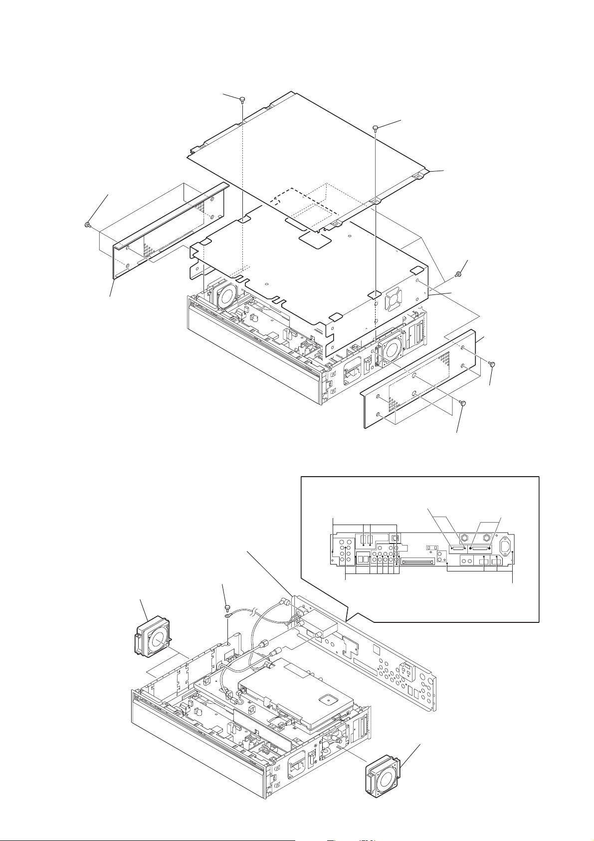
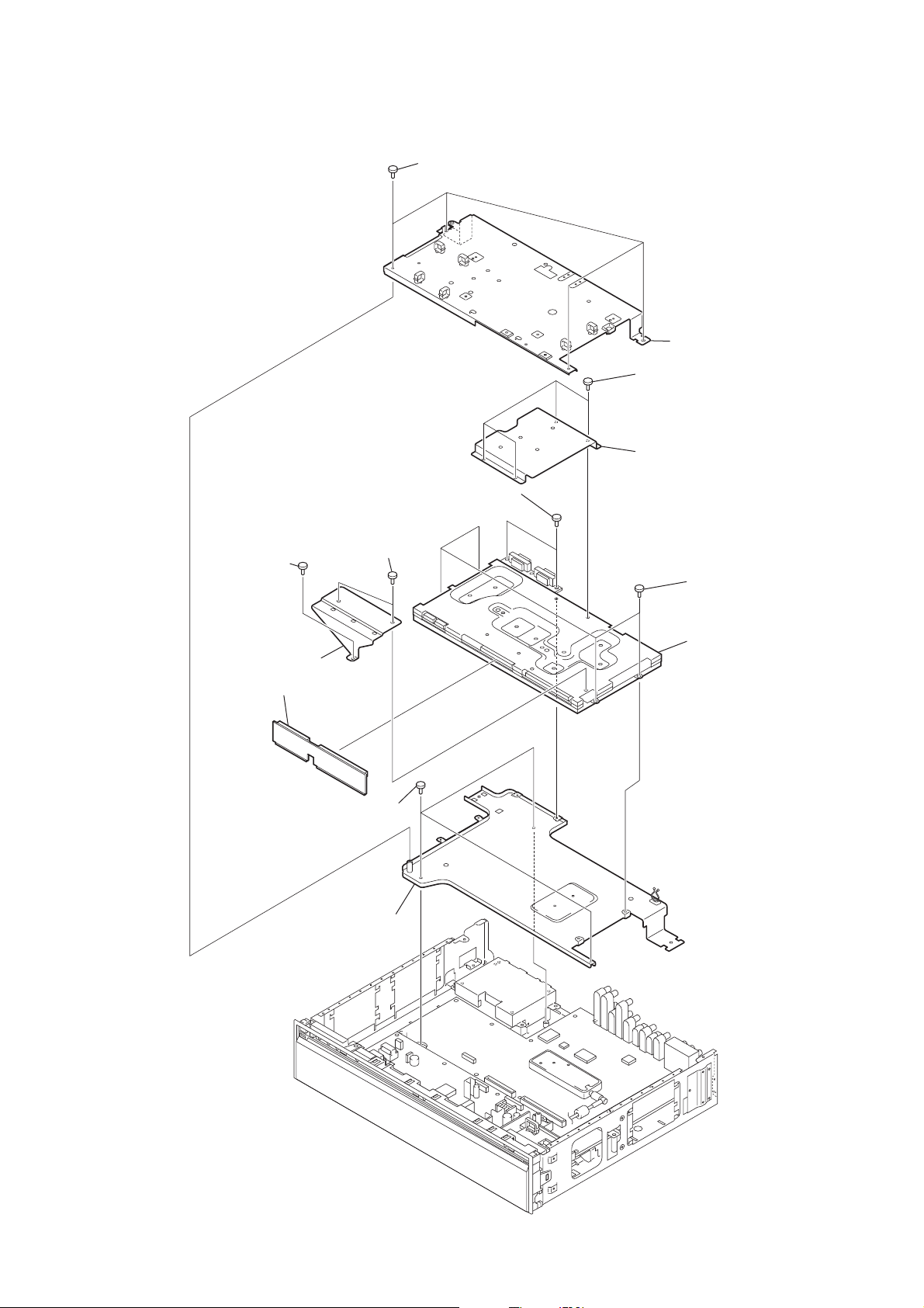
2-2. MEDIA RECEIVER UNIT (MBD-Q005)
2-2-1. TOP AND SIDE PANEL REMOVAL
6 One screw
(+PSW 3X6)
6 One screw
(+PSW 3X6)
4 Four screws
((TP),FLAT HEAD)
5 Side panel assy (L)
2-2-2. REAR PANEL BLOCK ASSY AND FAN BLOCK ASSY REMOVAL
7 Top panel
8 Four screws
(+PSW 3X6)
9 Top cover assy
3 Side panel assy (R)
2 Four screws
((TP),FLAT HEAD)
1 Two screws
(FLAT HEAD (M4 GRIP))
7 Two Fan block assy (A)
6 Rear panel block assy
5 One screw
(+PSW 4X8)
4 Four screws
(+PSW 3X8)
1 Eight screws
(+BVTP 3X12)
2 Two screws
(GRIP,M2.6 S HEAD EG))
8 Fan block assy (B)
3 Two screws
(HEX)
4 Four screws
(+PSW 3X8)
KDX-46Q005 (UC) 2-6
Page 15
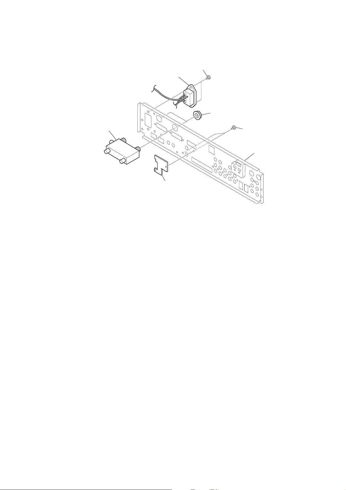
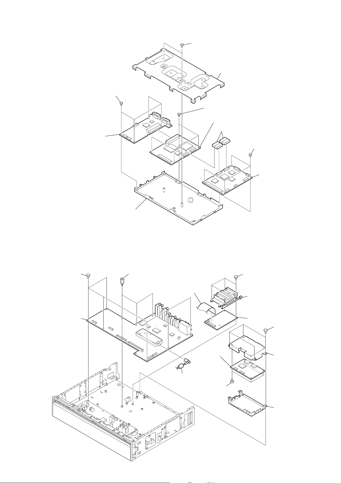
2-2-3. CSMU BOARD REMOVAL
5 Two screws
(+RK 3X8)
6 AC inlet
3 Two nuts with washer
4 Antenna switch
1 Two screws
(+PSW 3X8)
Rear panel
2 CSMU board
KDX-46Q005 (UC) 2-7
Page 16
2-2-4. QI, QMDV AND QT BOARDS REMOVAL
2 One screw
(+PSW 3X6)
3 Top ATSC shield (50)
qd Connector assy (FFC80P)
qh Three screws
(+PSW 3X6)
qj QT board
qf RF cable
qg Coaxial cable with
F-plug
6 Coaxial cable with
connector (LVDS)
1 ATSC shield sheet
9 Connector assy (FFC40P)
7 Four screws
(+PSW 3X5)
8 QMDV board
4 Coaxial cable with
connector (LVDS)
qk Four screws
(+PSW 3X6)
ql Bottom ATSC shield (50)
5 USB cable
0 Cord with connector
qs QI board
qa One screw
(+PSW 3X6)
KDX-46Q005 (UC) 2-8
Page 17
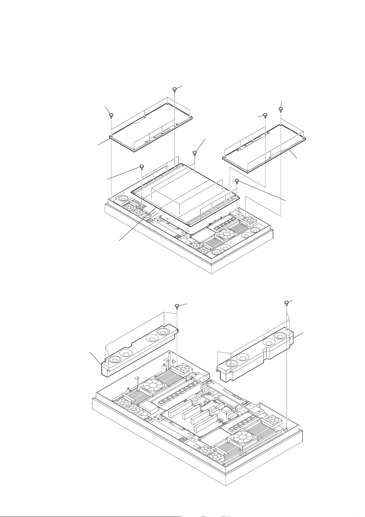
2-2-5. DDM BLOCK ASSY AND J1MU BOARD REMOVAL
1 Four screws
(+PSW 3X6)
8 Two screws
(+PSW 3X5)
2 Base plate assy (B)
6 Four screws
(+PSW 3X6)
7 Heat sink (DIC3)
3 One screw
(+PSW 3X10)
5 DDM support assy
qa J1MU board
qd Base plate assy (A)
4 Two screws
(+PSW 3X6)
9 Four screws
(+PSW 3X6)
0 DDM block assy
qs Three screws
(+PSW 3X6)
KDX-46Q005 (UC) 2-9
Page 18
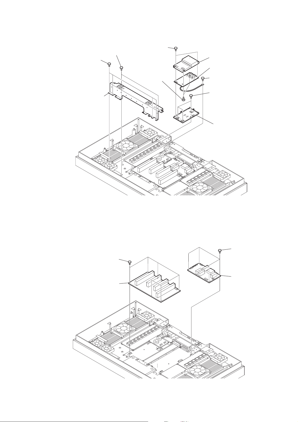
2-2-6. DIC3, M1MU AND T1MJ BOARDS REMOVAL
8 Four screws
(+PSW 3X5)
9 T1MJ board
1 Two screws
(+PSW 3X6)
2 DM shield (top)
6 Four screws
(+PSW 3X5)
7 DIC3 board
3 Board to board connecter 50P
4 Four screws
(+PSW 3X5)
5 M1MU board
0 DM shield (main)
2-2-7. A1MU, PD AND QUMU BOARDS REMOVAL
1 Six screws
(+PSW 3X6)
4 A1MU board
2 Three screws
(SPACER,HEXAGON (M3))
5 Connector assy
(FFC80P)
qs PD board
3 RF cable
6 Four screws
(+PSW 3X8)
7 PCMCIA card connector (frame)
8 QUMU board
9 Four screws
(+PSW 3X6)
0 PD shield (top)
qa Four screws
(+PSW 3X6)
qd PD shield (bottom)
KDX-46Q005 (UC) 2-10
Page 19
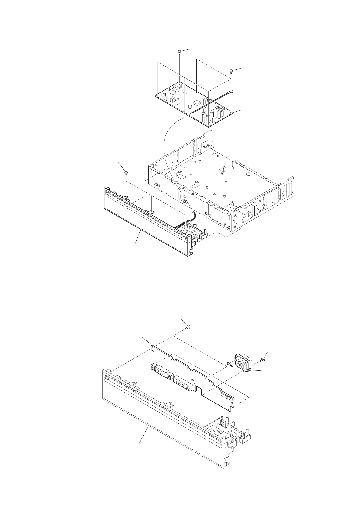
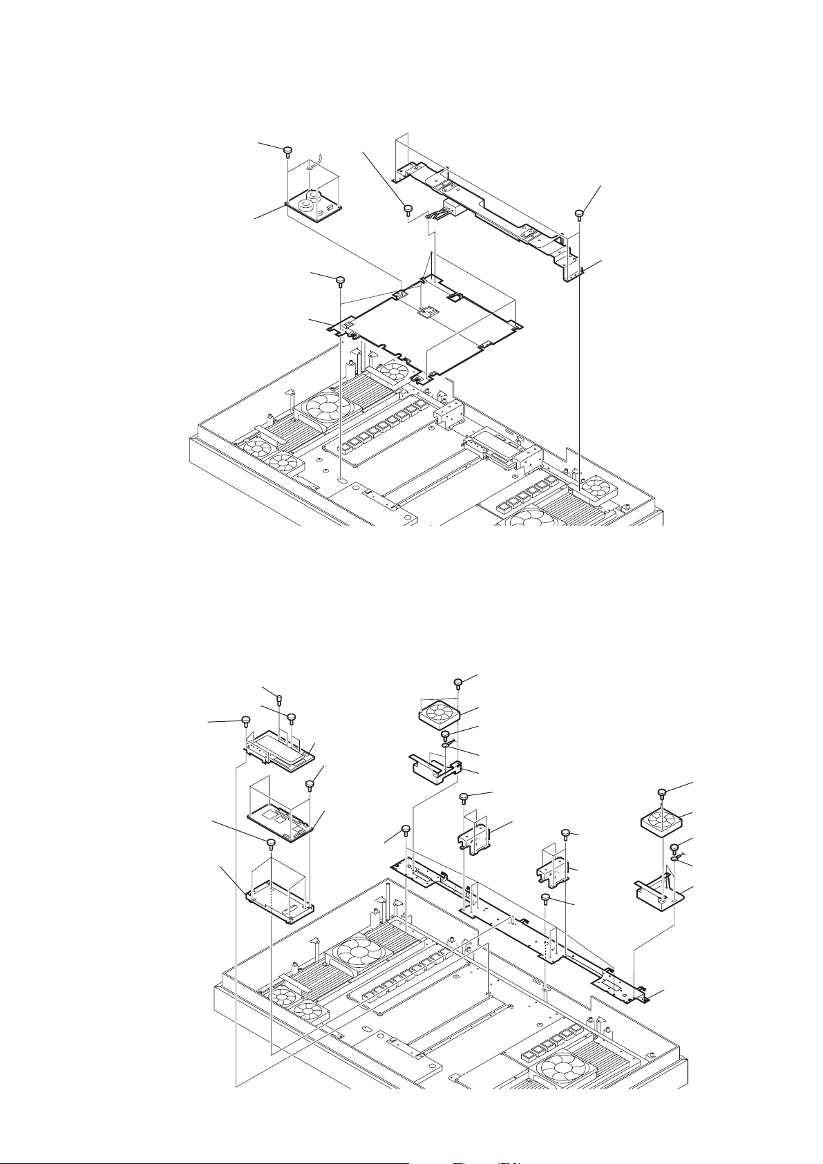
2-2-8. FRONT BLOCK ASSY AND G1MU BOARD REMOVAL
1 One screw
(+PSW 3X8)
4 Three screws
(+PSW 3X6)
2 Five screws
(+PSW 3X6)
3 G1MU board
5 Front block assy
2-2-9. H1MU BOARD REMOVAL
4 H1MU board
3 Four screws
(+BVTP 3X12)
1 Two screws
(+BVTP 3X12)
2 I-LINK cable cover
Front block assy
KDX-46Q005 (UC) 2-11
Page 20
2-2-10. QH BOARD REMOVAL
Front panel assy
3 Two screws
(+BVTP 3X12)
4 QH board
1 Two screws
(+BVTP 3X12)
2 HMBF Bracket
KDX-46Q005 (UC) 2-12E
Page 21
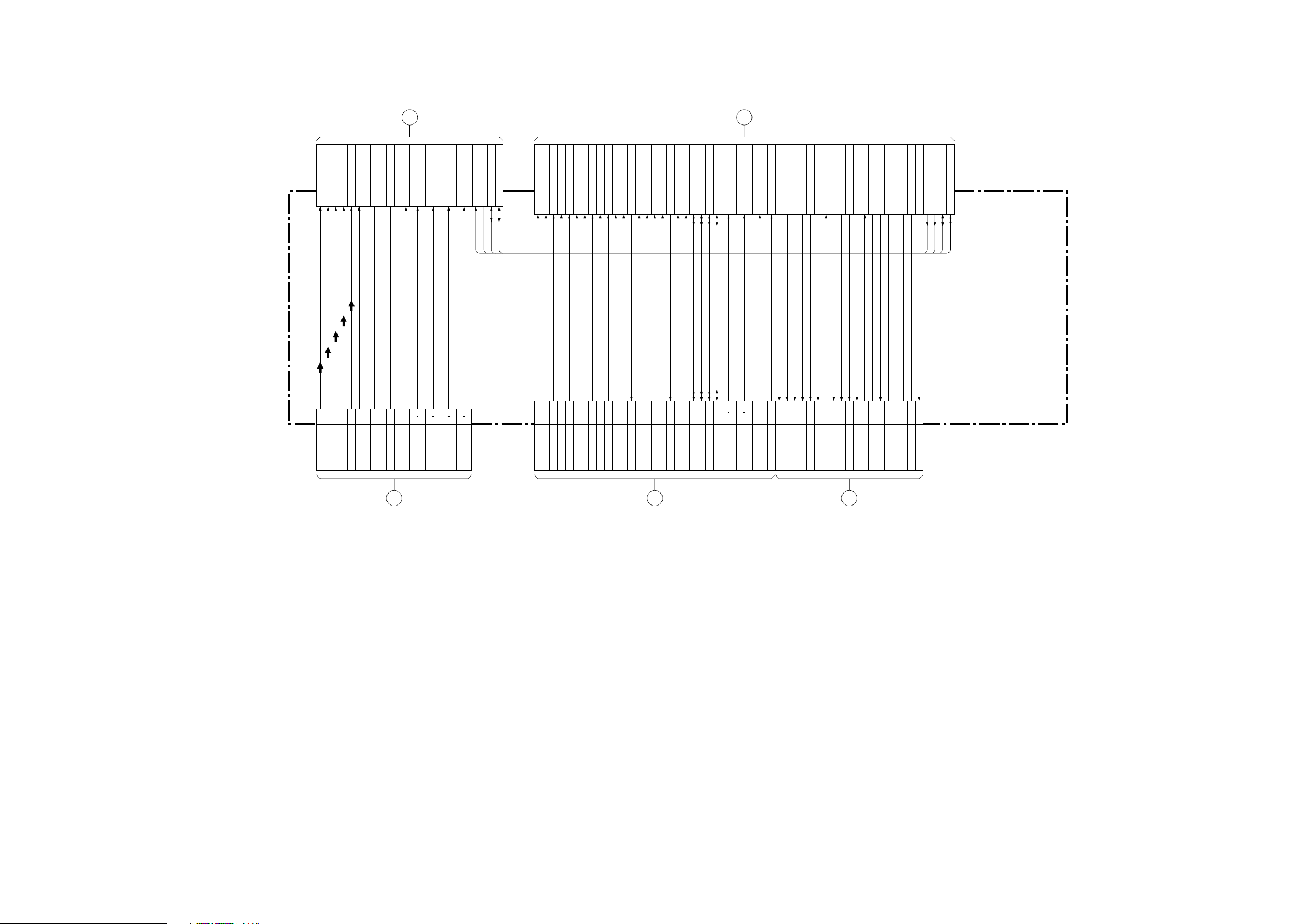
3-1. CIRCUIT BOARDS LOCATION
3-1-1. DISPLAY UNIT (XDM-F4600Q)
SECTION 3
DIAGRAMS
K board
G1B board
F board
DE6 board
3-1-2. MEDIA RECEIVER UNIT (MBD-Q005)
H1D board
G2L board
H2D board
A1MU board
G1MU board
H1MU board
PD board
CSMU board
QH board
QUMU board
J1MU board
T1MJ board
DIC3 board
QT board
QMDV board
QI board
M1MU board
KDX-46Q005 (UC) 3-1
Page 22
2
CN5407
1
.
.
3
4
.
5
6
.
9
10
.
7
8
.
11
12
.
13
14
.
15
16
.
19
20
.
17
18
26
27
30
88,49
TA1 +/-
TB1 +/-
46,47
TC1 +/-
43,44
TD1 +/-
39,40
TCLK +/-
41,42
TA2 +/-
36,37
TB2 +/-
34,35
TC2 +/-
31,32
TD2 +/-
27,28
TCLK2 +/-
29,30
R10
R17
8
8
R27
R20
8
G17
G10
8
G27
G20
8
B17
B10
8
B27
B20
7
HSYNC
8
VSYNC
9
DE
10
CLKIN
19
/PDWN
IC5408
LVDS TRANSMITTER
OVRED(OFR1_2-9)
OVRED(OFR2_2-9)
OVGRN(OFG1_2-9)
OVGRN(OFG2_2-9)
OVBLU(OFG1_2-9)
OVBLU(OFG2_2-9)
50
61
58
24
SDA0
28
SCL0
27
23
SET_ON
48
BUS_SW1
57
CMP_STOP
60
INT_V
25
PANEL_PD
55
3.3V
NVM_ERR
IC5102
DISPLAY ENGINE MINRO CONTROLLER
162
5
IC5908
37
Q5908
CN8200
1
5
2
14
12
4
IC5903
3
13
BA
SCK0
SDT0
SIN0
17
12
11
P61
P60
BINT
22
21
104
MD2
MD0
87
89
68
DE_BUSY
117
PICTURE_LED
118
TIMER_LED
119
POWER_LED
120
STBY_LED
98
MAIN SW
62
STBY_LO_INT
42
BL_IN
910
74
USB_DVP
73
USB_DVM
LIMITTER
Q5103
Q5205
HCONX
80
63
INV_FAIL
1
LED_RST
91
BUS_SW0
IC5107
6
1
5
2
73
64
SCL1
65
SDA1
BUS_SW2
49
95
ERR2
39
TEMP1
40
TEMP2
69
FAN
92
FAN ERR
96
97
93
94
ERR3
POWER
PANELON
ERR1
Q5101
82
CH_M/S_SW
CH_IIC_SW
81
SP PROT
102
OF_FLAG
8
K3.3V_SW
6
CH_NVM_WP
46
CH_RST
51
AUDIO RESET
100
SCLATCH
103
SCLATCH2
10
SDT1
19
SCK1
20
AUDIO
101
CN5104
STBY3.3V
CN5101
EXA SDA
EXA SCL
Q5104
MUTE
AMP
AUDIO RESET
LIMIT.
D5919
D5917
67
2
3
R0 +/-
2
R2 +/-
2
R1 +/-
2
RC +/-
2
HDMI-HPD
DSDA
DSCL
6
5
IC5902
3
B8
A13
A11
A10
A8
B7
A7
B6
A1
A3
A4
B5
CN5902
.
.
B11
B9
A6
76
32
BUS LINE BUFFER
IC5904
STBY3.3V
3
11
8
12
9
7
6
1
3
4
5
CN5103
7
21
Q8204
1
2
7
IC5103
STBY5V
3.3V
CN5106
5
3
2
1
6
7
8
9
STBY3.3V
STBY5V
CN5105
14
13
7-10
3.4
15
16
17
18
19
20
7
2
1
6
5
3
SUB6.5V
STBY5V
CN1001
5
4
3
1
6
7
CN1101
5
4
2
1
IC1101
SIRCS
ILLUMINANCE
IC1102
SENSOR
15
VCC OUT
H2D
H1D
D1001
Q1002
Q1005
Q1007
Q1008
D1002 D1003
25-28
21
IC5902
15
11
EXA SCL
EXA SDA
CN5901
PRO
DE6
IC5103
6
3
RG
CN5903
Q1003
Q1006
Q1001
Q1004
MICRO CONTROLLER
LVDS TRANSMITTER,
TO
G2L BOARD
CN6204
B
IC5110
CN2600
K BOARD
TO
A
TO
K BOARD
CN2603
C
UNIT
PDP
TO
5
7
8
9
4
5
4
3
1
6
7
8
9
10
11
12
13
14
13
12
11
10
9
8
7
3
4
5
6
15
16
17
18
DATAO
/CSO
ASD
VCC
SCK
SDT
SIN
STBY3.3V
RESET
SCL
SDA
BINT
P60
P61
MD0
MD2
SCLATCH
M_RST
CH_RST
CH_WP
3.3V_SW
OF_FLAG
A_MUTE
SP_PROT
DAT_D
CLK_D
CH_M/S_SW
CH_IIC_SW
AMP_RST
SCLATCH2
SCDT
SCSHIFT
TX00 +/-
TX01 +/-
TX02 +/-
TX03 +/-
TX0CLK +/-
TXE0 +/-
TXE1 +/-
TXE2 +/-
TXE3 +/-
TXECLK +/-
DCC
VCC
UDM
CABLE DET
JIG
VBUS
SCL
SDA
SET ON
POWER ON
SIRCS +/-
SPDIF +/-
XRESET
UDP
DE_REBOOT
SPDIF-
3.3V
STBY5V
BL_IN
SIRCS
STBY_LO
STBY
STBY5V
MUTE
TIMER
POWER
SCL
LED UPD
LED UDM
LED VBUS
SDA
PROTO
RSTX
MODE_SEL
PS_PROT
PANEL_ON
SUB_6.5V
STBY_5V
THERMO_1
THERMO_2
FAN_DRIVE
FAN_ERR
POWER_ON
AC_OFF_DET
P_VCC
G_PROT
POWER_LED
TIMER_LED
MUTE_LED
STBY5V
STBY_LED
STBY_LO
BL_IN
3.3V
SIRCS
STBY5V
9
2
LED_INT
Q5904
DISPLAY SIGNAL IN
(WHITE)
T1MJ BOARD
CN9008
RECEIVER
MEDIA
TO
TO
MEDIA
RECEIVER
CN9005
T1MJ BOARD
(BLACK)
DISPLAY SIGNAL IN
BUS LINE BUFF C
IC5906
3.3V_HP
Q5905
21
30,31
33,34
39,40
27,28
ADJ 0N/0P
ADJ 1N/1P
ADJ 2N/2P
AC KN/KP
IC5907
EQULIZER
20,21
17,18
13,14
23,24
ER0 +/ER1 +/ER2 +/ERC +/-
2
2
2
2
60,61
64,65
68,69
56,57
25CEHDMI_RST 99
RX0 +/-
RX2 +/-
RX1 +/-
RXC +/-
RESET
DSCL
DSDA
46
47
XTALOUT
XTALIN
X5901
27MHz
94
95
QO0-7
QO8-15
QO16-23
OE0-7
OE8-15
OE16-23
ODCK
VSYNC
HSYNC
DE
CSDA
CSCL
IC5910
PANEL LINK RECEIVER
45
46
IFQ(IFQ0_2-9)
IFQ(IFQ0_12-19)
IFQ(IFQ0_22-29)
IFQ(IFQE_2-9)
IFQ(IFQE_12-19)
IFQ(IFQE_22-29)
CLK
IFVSYNC
IFHSYNC
IFDE
8
8
8
8
8
8
IFQO
IFQO
IFQO
IFQE
IFQE
IFQE
BDDQ
ODA
BDDQ0-15
OBA0-11
16
12
9
DRAM
IC5301
DQ
A
OVRED1
OVRED2
OVGRN1
OVGRN2
OVBLU1
OVBLU2
DISPLAY ENGINE
IC5302
ONRED(OVRED1_0-9)
OVRED(OVRED2_0-9)
OVGRN(OVGRN1_0-9)
OVGRN(OVGRN2_0-9)
OVBLU(OVBLU1_0-9)
OVBLU(OVBLU2_0-9)
OVVS
OVHS
OVBLKDE
OVCLK2
DCC0
DCC1
CLX
ICFREE
BCSDA
ICSCL
D_DEV_RST
IC FREE
HDMI_RESET
CABLE_DET
STBY_5V
5
6
7
IC5901
BUFF INV.
Q5912
GND(DCC-SEL1)25
IC8209
OFHSYNC
OFVSYNC
OFDE
OFCLK
R15
STBY5V
DE_BUSY
B13
B12
D5921
5
6
IC5911
70
FPGA_BINT
2
5
73
1
6
7
1
2
IC5912
LINE RECEIVER
SPDIFSPDIF+
EXT_SCL
EXT_SDA
3.3V REG
1.5V REG
IC5105
IC8208
STBY3.3V
+1.5V
NON_PANEL_MODE
45
1.5V
1.8V
1.8V-HP
3.3V
FPGA_BINT
FPGA_SDA
FPGA_SCL
NVM_WP1
NON_PANEL_MODE
19
18
17
16
23
22
21
15
14
Q5106
SCL_JIG
SDA_JIG
STBY3.3V
SCL2
SDA2
5V_FPGL_SDA
5V_FPGL_SCL
3.3V
/CE
/CONFIG
CONF_DONE
DCLK
6
5
3
1
4
CONF_DONE
DCLK
nCOFFIG
nCE
DATAO
nCSO
ASDO
P17
R14
R13
SCL
SDA
WP
IC8207
6
5
7
FPGA_SCL
FPGA_SDA
DCLK
DATAO
NCS
ASDIO
IC8202
CONFIGURATION
ROM
5
2
1
7
10
10
10
10
10
10
3
Q8202,8203
IC5104
1
3
2
Q5901 RESET
IC5101
S5799
Q5102
90
RESET
1
2
4
IC5913
7
IC5911
2
1
STBY5V
Q5911
SWITCHING REG
OUT2
INV2
INV1
OUT1
STB
SEL1
19
Q5107
11
PS5101
16
OVP_DET
TMDS_ON
59
52
1
8
5
Q5108
+1.8V
Q5903
Q5902
D5109
IC5909
1.8V REG
3.3V_HP
1.8V_HP
D5110
+3.3V
+1.5V
+1.8V
1.8V_HP
+3.3V
IC5106
SCL2A
SDA2A
WP
66
67
6
5
799
SDA2
SCL2
NVM_WP1
LIMITTER
D5920
LIMITTER
IC5905
3,4 5
IC5109
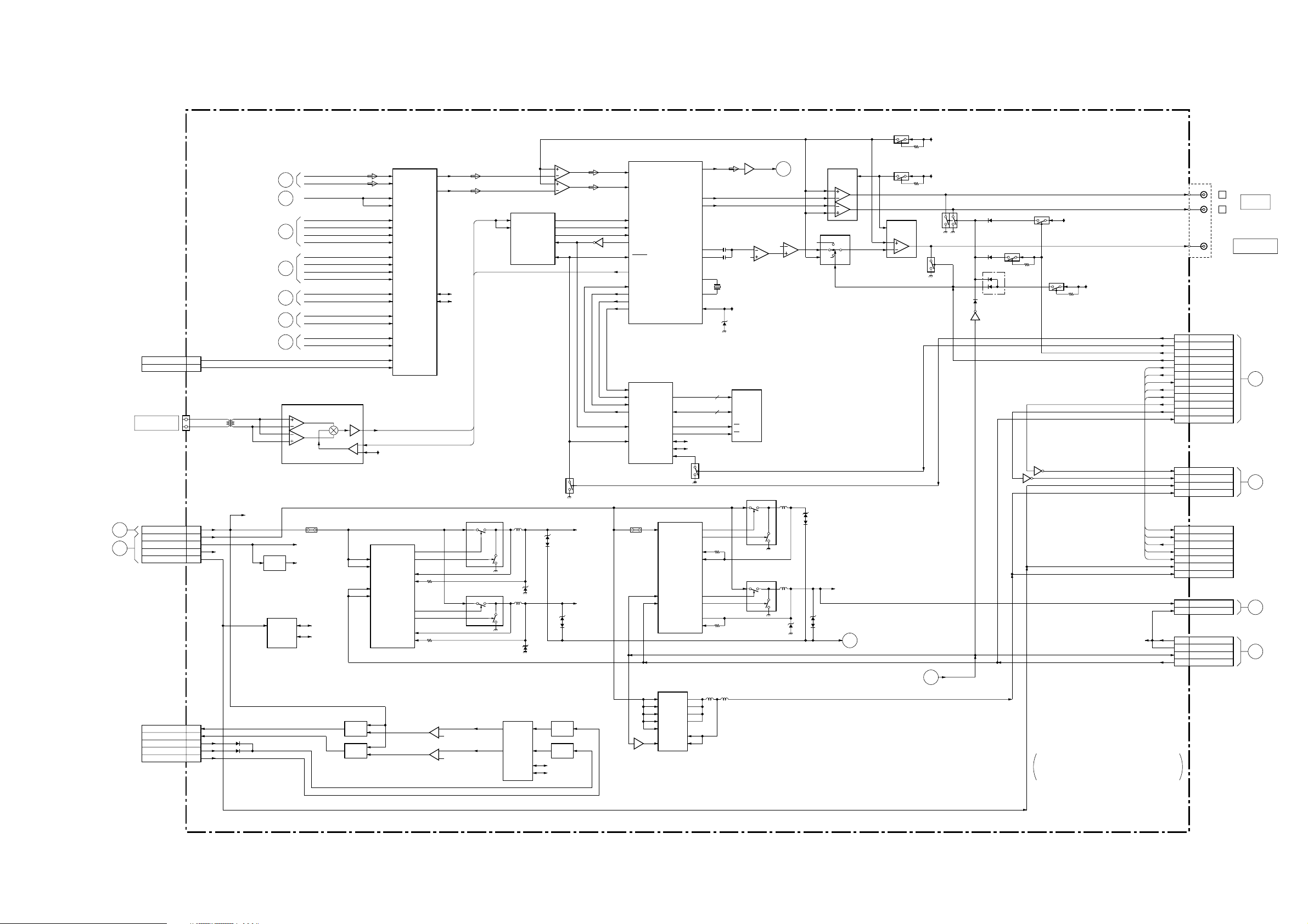
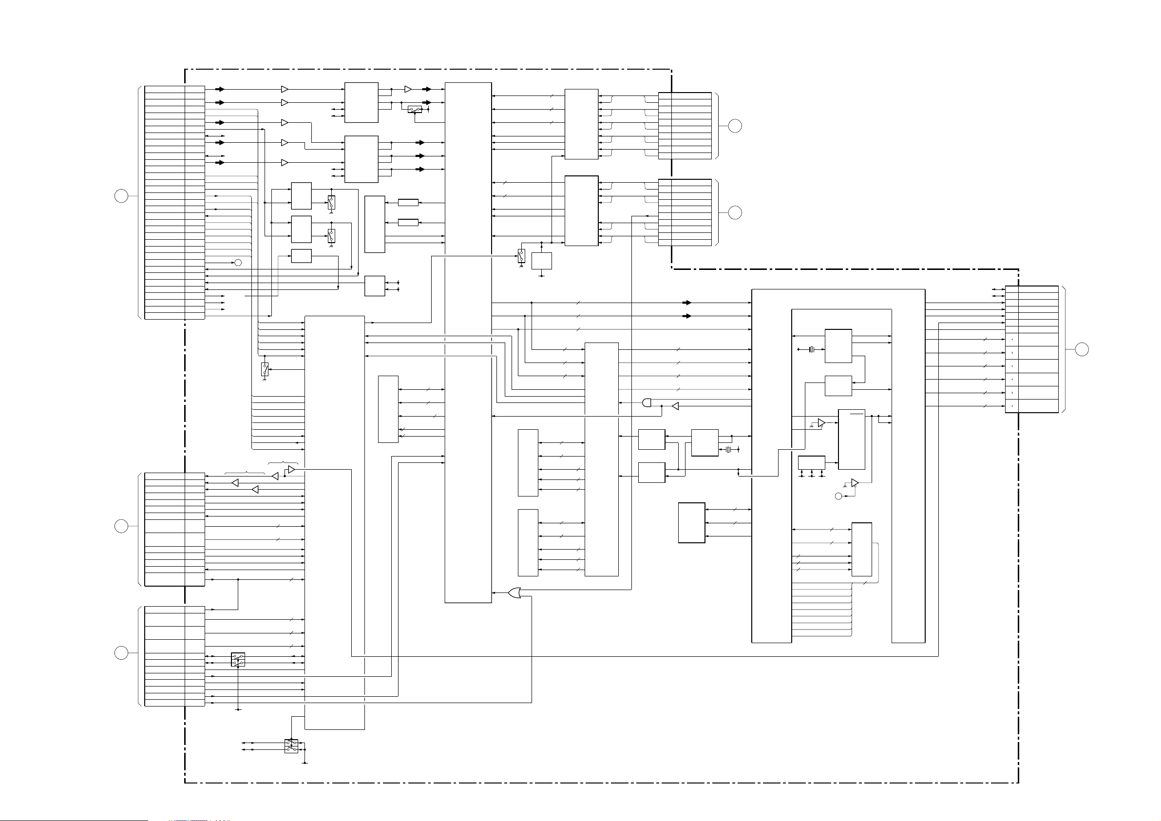
3-2. BLOCK DIAGRAMS
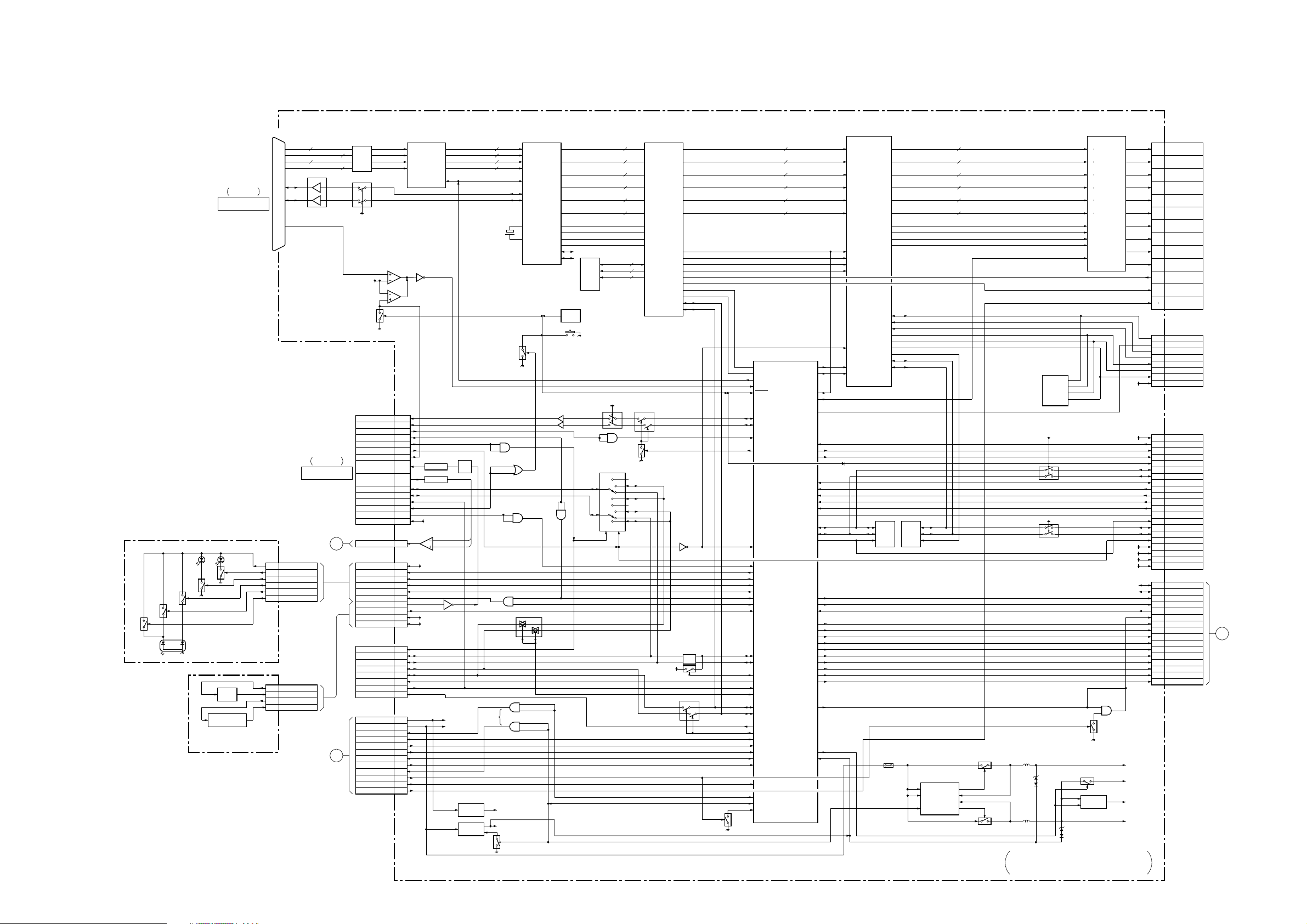
3-2-1. DISPLAY UNIT (XDM-F4600Q) (1) DE6, H1D and H2D Boards
KDX-46Q005 (UC) 3-2
Page 23
(2) K Board
C
TO
DE5 BOARD
CN5203
A
TO
DE5 BOARD
CN5105
D
TO
G2L BOARD
CN6206
CN2603
DAT_D
SLK_D
CH_M/S_SW
CH_IIC_SW
SP_PROT
A_MUTE
OF_FLAG
3.3V_SW
CH_WP
CH_RST
M_RST
SCLTCH
AMP_RST
SCLTCH2
SCDT
SCSHIFT
CN2600
SPDIF-
SUB11V
5V
3
4
5
6
7
8
9
10
11
12
13
14
15
16
17
18
6
3
1
OF_FLAG
SCDT
SCHIFT
IC2611
413
5
13
2
SP_PRT
A_MUTE
IC2612
1364
X2600
24.576MHz
IC6103
13
+3.3V
REG
IC2610
EEPROM
5
SDA
6
SCL
7
WC
D2627
INTERFACE RECEIVER
XMODE(I) DATA(O)
22
XIN(I)
3
DION(I)
2
8
Q2610
Q2611
IC2600
DIGITAL AUDIO
LRCK(O)
BLK(O)
ERROR(O)
CKOUT(O)
IC6102
1.8V
3.3V
REG
IC2603
DIGITAL AUDIO
PROCESSER
12
I2C_SDA
27
I2CM_S
13
I2C_SCL
26
RST
9
MCLKI
A_MUTE
SP_PRT
+3.3V
+1.8V
14
SDIN1
38
LRCLK
1
SCLKIN
IC2609
1
75
IC2601(2/2)
2
1
3.3V
DATA(O)
LRCK(O)
BLK(O)
1648
15
14
Q2602
34
13
45
SDOUT2
SDOUT1
3
4
3
5
IC2614
2
1
1
32
30
6
4
IC2602
RESET
SCDT
SCSHIFT
OF_FLAG
SCDT
SCSHIFT
OF_FRAG
X2601
49.152MHz
IC2607
12S PWM
31
DATA OUTL1
19
SOFMUTE
36
XFSIIN
21
SCDT
22
SCSHIFT
24
OVFFLAGR
25
OVFFLAGL
23
SCLATCH
29
LRCK
30
BCK
27
INIT
IC2604
12S PWM
31
27
INIT OUTL2
30
BCK
29
LRCK
23
SCLATCH
21
SCDT
22
SCSHIFT
24
OVFFLAGR
25
OVFFLAGL
19
SOFMUTE
36
XFSIIN
48
XFSOIN
OUTL2
OUTL1DATA
OUTR1
OUTR2
11
9
11
9
6
4
IC2608
AUDIO POWER(W)
2
17
PWM_AP OUT_A
4
/RST
IC2606
AUDIO POWER(L)
2
PWM_BP
17
PWM_AP
4
/RST
IC2605
AUDIO POWER(R)
2
17
PWM_AP OUT_A
4
/RST
IC2601(1/2)
10
8
9
Q2603
OUT_BPWM_BP
DREG
/SD
OUT_B
OUT_A
DREG
/SD
OUT_BPWM_BP
DREG
/SD
11
30
25
8
13
30
25
8
13
30
25
8
13
W+
W-
Q2608,Q2609
DC
DETECT
L+
L-
Q2605,Q2607
DC
DETECT
R+
R-
+12V
Q2604,Q2606
DC
DETECT
3
IC6101
+12V REG
2
1
12
13
Q6101
Q6102
D2624
D6101
AUDIO PROCESSOR,
K
AUDIO OUTPUT
1
2
3
4
5
6
1
2
CN2601
W+
WL+
LR+
R-
CN2602
AUDIO_VCC
WOOFFER
L
R
E
TO
G2L BOARD
CN6207
KDX-46Q005 (UC) 3-3
Page 24
2
1
AC(L)
AC(N)
CN6001
CN6018
1
2
AC(L)
AC(N)
CN6100
RECT
D6201
OUT
VCC
CTL
IC6300
18V REG
7
4
3
PFC OUT
PRI_VCC1
PFC DET
CN6101
L6200-L6202
D6210
Q6200-Q6202
PFC SW
31RLY-ON
RLY-5V
CN6200
3
1
2
Q6302
Q6301
OVP
PROTECT
IC6202
1
14
2
3
13
12
LATCH
Q6303
IC6203
VREF
LVP
Q6209
5
6
10
9
7
8
Q6205
SS
OUT
VCC
VREF
CAOUT
SS
VFB
LATCH
RV6200
13
11
SS
Q6207
16
15
9
3
(POWER SUPPLY)
G1B
IC6201
DRIVE
Q6208
GND/BL_ON
P_SW<->
4
5
Q6305
PH6301
F
L6004-6005
PH6300
Q6100
Q6306
STBY5V
Q6304
D6208
T6600
2
6
8
4
D6606
STBY5V
11
10
2
VCC
8
7
DRAIN
DRAIN
5
STARTUP
4
VFB
PH6600
D6604
TH6600
D6600 D6605
IC6600
CONVERTER
D6607
AC INLET
RY6001 RY6101
1
2
1 PRI_VCC2
6 STBY5V
IC6601
1
D6200
D6220
D6202
D6221
TH6300
Q6300
Q6204
Q6206
PFC DRIVE
8
6
Q6210,Q6211
Q6203
IC6200
F6001
IC6400
Q6400
Q6407,Q6408
6
8
PFC DRIVE
Q6403
Q6401
Q6500
TH6500
D6421
D6411
D6420
D6409
Q6504
STBY5V
PH6500
PH6501
Q6505
Q6405
DRIVE
IC6401
3
9
15
16
Q6404
SS
11
13
RV6400
LATCH
VFB
SS
CAOUT
VREF
VCC
OUT
SS
Q6402
8
7
9
10
6
5
Q6406
LVP
VREF
IC6403
Q6503
LATCH
12
13
3
2
14
1
IC6402
PROTECT
OVP
Q6501
Q6502
2
1
3
PFC SW
Q6409-Q6411
D6419
L6400-L6402
18V REG
IC6500
CTL
VCC
OUT
D6410
RECT
D6417
CN6102
3 PFC_OUT
Q6507
Q6506
D6502
H
CN6210
G2L BOARD
TO
F
G
TO
G2L BOARD
CN6208
CN6203
G2L BOARD
TO
D6301
D6213
D6212
D6501
D6401
D6402
3
(3) F and G1B Boards
KDX-46Q005 (UC) 3-4
Page 25
(4) G2L Board
H
TO
G1B BOARD
CN6102
F
TO
G1B BOARD
CN6101
CN6210
PFC_OUT
CN6208
PRI_VCC2
PFC_DET13
PRI_VCC1
PFC_OUT47
D6422
PH6474
Q6470
Q6471
PS6800
IC3004
REG
1
Vin Vout
CTRL
IC3001
CONVERTER
18
VCC OUT1
7
DTC2
3
2
INV1
OUT2
INV2
TH3000
IC3005
4
11
16
9
5
1
3
Q3001
Q3002
L3001
L3002
D3006
D3008
L3003
L3004
D3024
Q3009
Q3004
PS_PROT
PANEL_ON
PS_PROT
Q3007
Q3008 11
CN6207
1
.
AUDIO_VCC
2
CN6204
3
STBY5V
.
4
7
SUB6.5V
10
PANEL_ON
13
PS_PROT
14
THERMO_1
15
FAN_DRIVE
17
FAN_ERR
18
POWER_ON
19
20
AC_OFF_DET
21
G_PROT
25
P_VCC
28
CN3005
1
FAN1
4
FAN2
7
FAN3
10
FAN4
2
FAN_ERR1
5
FAN_ERR2
8
FAN_ERR3
FAN_ERR4
CN6203
1
PLY_5V
3
PLY_ON
4
GND/BL_ON
5
P_SW<->
6
STBY5V
CN6206
1 SUB6.5V
3 SUB_11V
CN6202
SUB_11V
21BL_ON
E
TO
K BOARD
CN2602
B
TO
DE6 BOARD
CN5105
TO
FAN
G
TO
G1B BOARD
CN6200
D
TO
K BOARD
CN2600
TO
LC BOARD
3
D6700
1
2
15
IC6700
DRIVE
VSENSE
F/B
VC1
VG(H)
VS
VG(L)
OCP
23
22
20
16
Q6700
CONVERTER
Q6701
CONVERTER
D6709
2
4
6
7
T6700
PIT
PH6700
D6801
D6804
16
15
14
D6807
12
13
10
D6806
11
9
IC6800
PS3000
G2L
(POWER SUPPLY)
Q3000
Q3003
PANEL_ON
KDX-46Q005 (UC) 3-5
Page 26
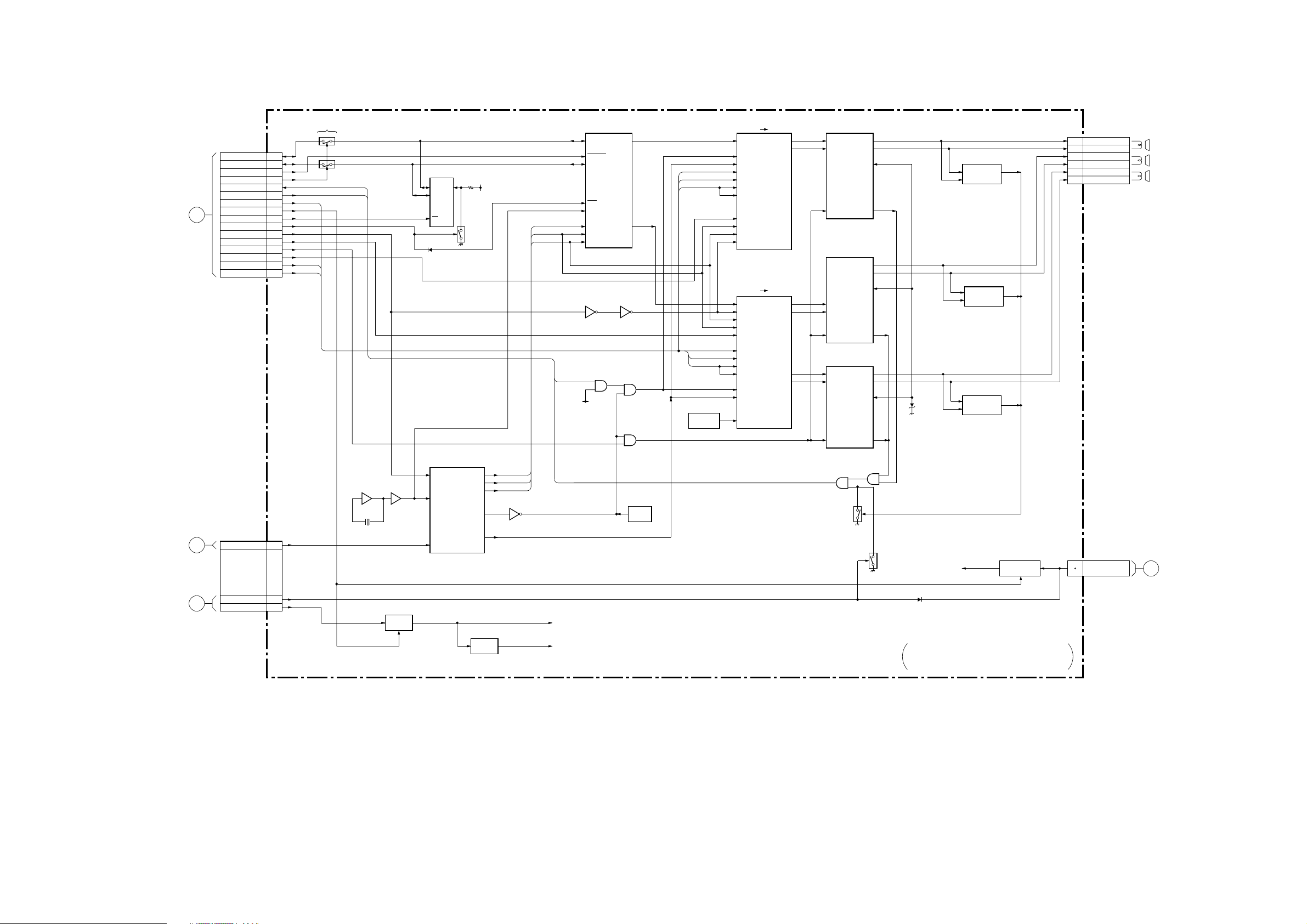
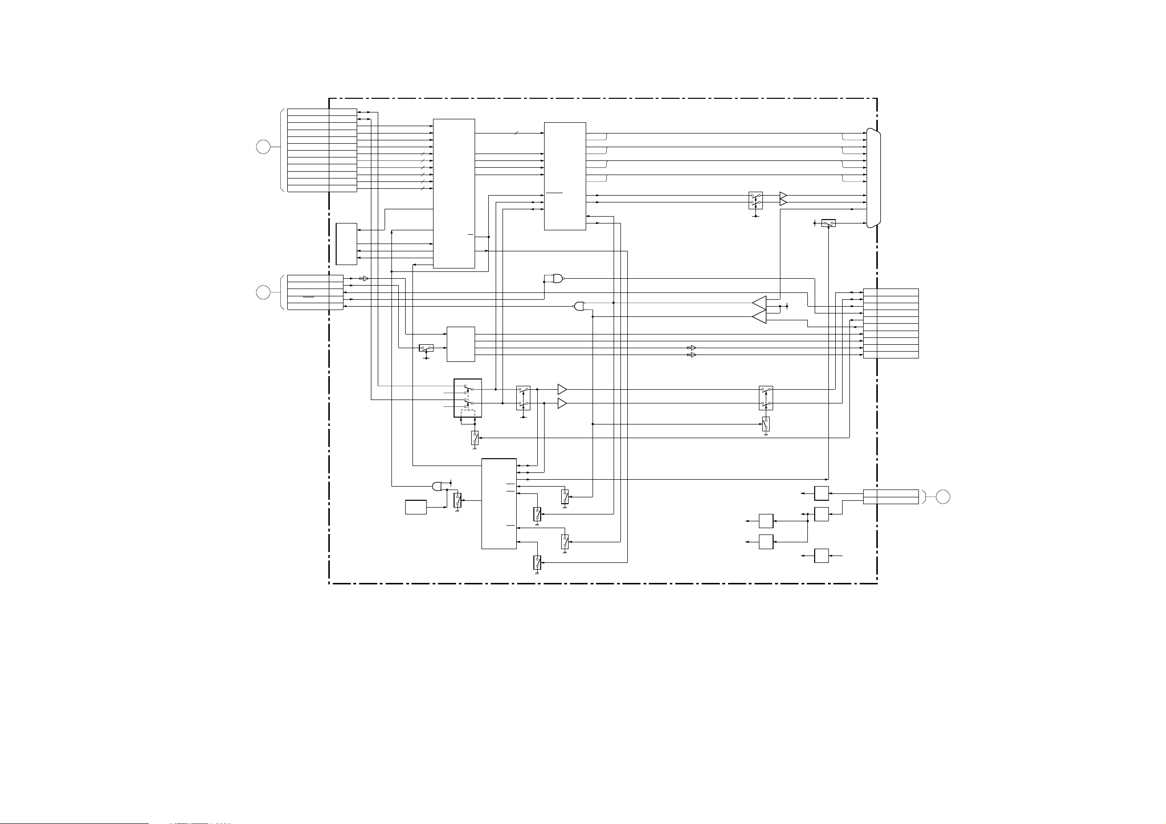
3-2-2. MEDIA RECEIVER UNIT (MBD-Q005) (1) A1MU(1/2), CSMU and H1MU(1/2) Boards
QT BOARD
CN7901
VIDEO IN
1
VIDEO IN
3
HD/DVD IN
4
HD/DVD IN
5
PD BOARD
CN9504
A
TO
AUDIO
AUDIO
AUDIO
AUDIO
B
TO
S VIDEO
VIDEO
L
(MONO)
R
S VIDEO
VIDEO
L
(MONO)
R
Y
B
P
R
P
L
R
Y
B
P
R
P
L
R
CN102
AFTM
TU1V
TU1R
TU1L
SCLK
SDAT
AGC_MUTE
TU100
SUB TUNER
DET_OUT
DE_EM
AFT_OUT
5V(TU)
5V(IF)
5V(D-D)
J100
J101
J102
J103
J104
CN101
Y
L
R
RESET
SDA
SCL
9V
1
2
4
6
8
9
10
Q108,111,118
CL
SCL_M
DA
SDA_M
A_5V
34
12
43
21
S3_SSW
13
7
6
2
4
3
1
TUNER AUDIO R
TUNER AUDIO L
SCL_M
SDA_M
Q115
V1_Y
V1_C
V1_V
V1_L
V1_R
V3_Y
V3_C
V3_V
V3_L
V3_R
VG_1
VB_1
VR_1
C1_L
C1_R
VG_2
VB_2
VR_2
C2_L
C2_R
HDMI_L
HDMI_R
SDA_M
SCL_M
SW9V
Y
DE-EM
TO 2/2
TO 2/2
VIDEO
1
TO 2/2
2
TO 2/2
3
4
5
TO 2/2
Q109
Q103
A1MU(1/2)
(VIDEO SW)
INPUT TERMINAL
AFT1
M_HSYNC
AGC1
S_HSYNC
AFT2
V1_V
V1_Y
V1_C
V3_V
V3_Y
V3_C
S3_SSW
Q107,110
VG_1
VB_1
VR_1
VIDEO
79
Q112,114,116,117
VG_2
VB_2
VR_2
Y DETECT
11
12
13
14
17
18
19
16
33
34
35
40
41
42
26
1
IN1_CV
IN5_S
IN2_CV
CV
Y
C
CV
Y
C
S
Y
CB
CR
Y
CB
CR
IN8_Y
TO 2/2
TO 2/2
VIDEO SW
IN5
IN6
IN9
IN10
6
7
IC101
CV/YOUT1
C/CBOUT1
CROUT1
SEL_OUT1
SYNC_OUT1
CV/YOUT2
C/CBOUT2
EXT_CLK/XTAL
SCL
SDA
CV
Y
IN4
C
S
V2_SSW
V2_C
V2_Y
V2_V
V2_L
V2_R
PC_L
PC_R
ATSC5V
D5V
Q102
58
Q101
59
Q100
60
Q103
56
55
Q104
67
Q105
68
X100
4MHz
51
76
SCL_M
77
SDA_M
7
8
9
10
V2_V
V2_Y
V2_C
V2_SSW
CN104
1
4
6
8
10
12
14
16
18
D5V(SW_5V)
20 20
V/Y
B-Y
R-Y
SUB_Y
SUB_C
CN1507
S_SW2
1
C2
4
Y2
6
V2
8
L2
10
R2
12
PC_L
14
PC_R
16
ATSC_5V
ATSC5V
18
SW5V
H1MU(1/2)
FL1500
D_OVP
9
TO 2/2
IC002
1,2
4
TB1500
43
21
TO 2/2
VIDEO
(MONO)
J1500
PC IN
AUDIO
Q012
AC_RLY
10
S VIDEO
L
R
AUDIO
8
VIDEO IN
2
Q001-007
SPDIF
INV
SUB_C
SUB_Y
AFT1
AFT2
AGC1
M_HSYNC
S_HSYNC
STBY5V
SW3.3V
ATSC5V
AUDIO L/R
V/Y
B-Y
R-Y
SW2.5V
SW3.3V
D5V
SUB6.5V
SDA_M
SCL_M
SDA_M
SCL_M
SDA_S
SCL_S
D5V
CN005
B32
I_MAIN_G
B38
I_MAIN_CV
B34
I_MAIN_B
B40
I_MAIN_C
B36
I_MAIN_R
A36
SET_ON
B27
I_USBCONNECT
B26
I_USBDMNS
B24
I_USBDPLS
A21
I_UARTTXDP
A19 I_UARTRXDP
A34
D_OVP
A16
|
SW_2.5V
B17
A13
|
SW_3.3V
B14
A11
SW_5V
B11
A7
|
SUB_6.5V
B8
CN002
IFP_VBUS
14
13
IFP_UDM
12
IFP_UDP
11
TVM_VBUS
10
TVM_UDM
9
TVM_UDP
7
B_INT
6
I2C_DAT
5
I2C_CLK
4
U2_TX
3
CONTROL_S_OUT
2
MAIN_LOG
1 CONTROL_S_IN
CN003(1/2)
B42
CVY_MAIN
B38
SUB_C
B40
SUB_Y
B26
D_OVP
B20
A23
JIG_UDP
A24
JIG_UDM
A17
B_INT
A21
USER_TXD
A22
USER_RXD
A53
AFT_MAIN
A50
AFT_SUB
B51
AGC_ATT
A49
TU_H_MAIN
A48
TU_H_SUB
A33
HDMI_RST
B10
CABLE_DET
B27
AC_RLY
A27
SET_ON
A25
SIRCS
A20
I2C_SDA
A19
I2C_SCL
B16
SDA_S
B15
SCL_S
B59
|
STBY5V
B60
A57
|
B58
A43,A44
SW_3.3V
A45,A46
B45
ATSC_5V
CN001
9
CABLE_DET
8
7
SET_ON
5
SIRCS
3
SPDIF-
VBUS
D5V
P_ON
C
TO
J1MU BOARD
CN5001
CN1802
19
17
15
13
11
9
7
6
5
4
3
2
1
CSMU
D
TO
J1MU BOARD
CN5003
E
TO
T1MJ BOARD
CN9004
CN1800
10
IFP_VBUS
9
IFP_UDM
8
IFP_UDP
7
TVM_VBUS
6
TVM_UDM
5
TVM_UDP
3
B_INT
2
DAT_S
1 CLK_S
J1801
CONTROL_S
OUT
J1800
CONTROL_S
IN
KDX-46Q005 (UC) 3-6
Page 27
(2) A1MU(2/2) Board
CN103
L
R
TB100
CENTER SPEAKER
IN
CN602
SUB11V_B
SUB11V
SUB6.5V
SW9V
THRU5V
CN004
FAN1
FAN2,3
FAN_ERR2
FAN_ERR3
FAN_ERR1
QMDV BOARD
TO
G1MU BOARD
CN6403
TO
G1MU BOARD
CN6401
TO
CN7309
F
G
TO
FAN
4
2
1
3,4
7,8
11,12
15
1
4,7
5
8
2
T100
SUB_11V_B
SW9V
ATSC5V 1
D007
D008
TO 1/2
MTU_L 22
1
DE-EM
2
TO 1/2
V1_R 2
V3_L 4
3
V3_R 5
TO 1/2
C1_L 10
4
TO 1/2
HDMI_L 16
HDMI_R 17
5
TO 1/2
6
TO 1/2
PC_L
PC_R
7
TO 1/2
IC100
OP AMP
3
4
6
7
PS601
SUB6.5V
IC103
13
5V REG
THERMO SENSOR
IC001
VCC SDA
SCL
A5V
2
SDA_S
SCL_S
TUNER AUDIO L
TUNER AUDIO R
5
2
1
6
NC
24
VCC
9
STBY1
10
STBY2
IC003
1
3
FAN
2
DRIVE
IC004
1
3
FAN
2
DRIVE
AUDIO SW
IN8_L
23MTU_R
IN8_R
25
IN9_L
26
IN9_R
1V1_L
IN1_L
IN1_R
IN2_L
IN2_R
IN4_L
11C1_R
IN4_R
13C2_L
IN5_L
14C2_R
IN5_R
IN6_L
IN6_R
19V2_L
IN7_L
20V2_R
IN7_R
7
IN3_L
8
IN3_R
28
IN10_L
29
IN10_R
SW9V
IC602
DC-DC CTRL
OUT1_U
OUT1_D
LL1
INV1
OUT2_U
OUT2_D
LL2
INV2
IC102
29
27
28
1
17
19
18
14
LOUT1
ROUT1
SCL
SDA
IC006
4
IC007
4
39
37
31
32
1
3
1
3
AUDIO L
AUDIO R
SCL_M
SDA_M
CENT
POL
CENT
Q606
3.3V REG
Q604
2.5V REG
A/D CONVERTER
1
AINR
2
AINL
L605
L603
IC009
DAC
7
DAC0
6
DAC1
IC4000
D607
D609
SW0
SW1
SCL
SDA
2
1
15
14
IC409
3
2
5
6
SDT0
LRCK
SCLK
MCLK
PDN
D615
D617
Q008,010
Q009,010
SCL_S
SDA_S
AMP
9
10
12
11
13
SW
SW
AUDIO L
1
AUDIO R
7
D612
D616
Q402
RESET
SW3.3V
SW2.5V
42
IC401
AUDIO PROCESSOR
56
SC1_IN_L
SC1_IN_R
57
7
I2S_DA_IN1
5
I2S_WS
4
I2S_CL
74
AUDIO_CLOCK_OUT
21
RESET
78
DIGITAL_CONTROL
_OUT_0
8
I2S_DEL_IN
9
I2S_DEL_OUT
10
I2S_DEL_CL
11
DVSUP
IC403
AUDIO DELAY IC
7
LR_CLK
8
BIT_CLK
13
IISM_IN
59
IISM_OUT
11
FCLK
18
RST
PS600
24
9
10
DC_DC CONVERTER
6
18
19
20
21
Q700
1
IC402
SPDIF_OUT
SC1_OUT_L
SC1_OUT_R
SC2_OUT_R
SC2_OUT_L
XTAL_OUT
A0
|
A16
IO0
|
IO7
22
FWR
29
FRD
2
SCL
3
SDA
6
MUTE
IC601
DC_DC CTRL
VCC
STBY1
STBY2
IC700
VCC
VOUT
VDD
VOUT
VDD
VOUT
VDD
VOUT
VDD
OCL+
R/C
OCL-
X400
18.432MHz
IC404
17
8
29
24
SW9V
IC406
SDRAM
A0
|
A16
IO0
|
IO7
WE
OE
Q400
SPDIF
3
Q603
REG
Q605
5V REG
IC405
1
8
TO 1/2
6
5
L602
L604
D608
76 IC410
AUDIO L/R
37
38
33 2
34
71
XTAL_IN
72
39
AHVSUP
A0-A16
IO0-IO7
SCL_M
SDA_M
Q403
MUTE
29
OUT1_U
27
OUT1_D
1
INV1
28
LV1
17
OUT2_U
19
OUT2_D
18
LL2
14
INV2
L701 L702
11
12
13
14
25
27
Q401
BIAS
Q408
8
V+
5
6
2
3
6
7
7
3
D610
D613
D611
D614
D_OVP
7
1
IC407
1
5
D5V
9
TO 1/2
9V SW
IC408
8
V+
3
2
Q405
MUTE
1
10
TO 1/2
SW9V
SW9V
Q407
Q407 Q406
MUTE
AC RLY
D412
D407
D411
Q411
INV
D404
ATSC9V
Q410
Q412,413
Q404
Q608
Q607
STBY5V
D5V
STBY5V
A47
B46
A32
B31
B44
B43
A36
A35
A34
A30
A29
A28
1
3
4
5
1
3
5
6
7
9
13,14
3,4
1
1
2
4
6
J400
L
R
CN003(2/2)
AD_RST
AD_MUTE
LINE_MUTE
SP_MUTE
IFP_H
IFP_V
ATSC_RXD
ATSC_TXD
ATSC_RST
ANT_S
ANT_M
POW_CTL
CN605
MS1
MS2
5V
9V
CN603
IFP_H
IFP_V
ATSC_RXD
ATSC_TXD
ATSC_RST
ATSC_5V
ATSC_11V
CN601
SW_5V
STBY5V
CN606
STBY5V
P_SW(-)
AC_RLY
REC_ON
AUDIO OUT
(VAR/FIX)
SUB WOOFER OUT
(VAR)
H
TO
J1MU BOARD
CN5003
AA
TO
QMDV(2/2)BOARD
CN7300
K
TO
T1MJ BOARD
CN9003
L
TO
G1MU BOARD
CN6402
A1MU(2/2)
AUDIO PROCESSOR
POWER SUPPLY
ATSC5V
KDX-46Q005 (UC) 3-7
Page 28
(3) J1MU Board
CN5000
I_MAIN_G
A9A3A7
V/Y
V/Y
B32
I_MAIN_B
I_MAIN_C
I_MAIN_R
I_MAIN_CV
A5
A1
R-Y
B/Y
B-Y
B36
B40
B34
B38
SET_ON
I_USBDMNS
I_USBDPLS
I_USBCONNECT
B5
A15
A14
A17
B24
B26
B27
A36
M
D_OVP
SW_2.5V
I_UARTTXDP
I_UARTRXDP
B20
B22B7A24
A16
A34
A19
A21
B25
B17
A27
A13
SW_3.3V
TO
DIC3 BOARD
CN4000
SW_5V
B30
B28
A30
A33
A7
B14
B11
A11
B_INTB2
SUB_6.5V
SYSTEM_RSTA31
B34
B8
TO
D5
B4
SW_3.3V
ATSC_5V
A16
B15,B16
B17,B18
M1MU BOARD
CN7004
AD_RST
SP_MUTE
AD_MUTE
LINE_MUTE
A15
B14
B29
A30
IFP_H
IFP_V
A17
A18
ATSC_RXD
ATSC_TXD
ATSC_RST
B25
B26
B27
ANT_S
ANT_M
B31
B32
FMONO
POW_CTL
ATSC_OVP
B7
B9
B33
O_SAP
I_SAP
B10
A11
YOBI_2
YOBI_1
WOOFER_MUTE
A13
A14
B30
SDA_1
SCL_1
IFP_BINT
SYSTEM_RST
A37
A47
A48
A49
N
VBUS
SUB_C
CN5004
CVY_MAIN
A19
A23
SUB_Y
D_OVP
A35
A21
JIG_UDP
A41
B38
B_INT
JIG_UDM
USER_TXD
B37
B44
B40
AFT_SUB
USER_RXD
AFT_MAIN
B39B8B11
AGC_ATT
TU_H_SUB
TU_H_MAIN
A10
B12
B13
SDA_1B8
SCL_1B6
AC_RLY
HDMI_RST
CABLE_DET
A51
B28
A34
SIRCS
SET_ON
B34
B36
SDA_M
SCL_M
B41
B42
SDA_S
SCL_S
A45
A46
STBY5V
A1
A2
A3
J1MU
B42
B38
B40
B26
B20
A23
A24
A17
A21
A22
A53
A50
B51
A49
A48
A33
B10
B27
A27
A25
A20
A19
B16
B15
B59
B60
A57
B58
A43,A44
B45
A47
A45,A46
B46
A32
B31
B44
B43
A36
A35
A34
A30
A29
A28
(RELAY BOARD)
A31
CN5001
I_MAIN_G
I_MAIN_R
I_MAIN_C
I_MAIN_B
I_MAIN_CV
SET_ON
I_USBDPLS
I_USBDMNS
I_USBCONNECT
D_OVP
SW_2.5V
I_UARTRXDP
I_UARTTXDP
A1MU(1/2)BOARD
SW_5V
SW_3.3V
TO
CN005
SUB_6.5V
CN5003
CVY_MAIN
SUB_Y
SUB_C
VBUS
D_OVP
B_INT
JIG_UDM
JIG_UDP
USER_RXD
USER_TXD
AFT_MAIN
AFT_SUB
AGC_ATT
TU_H_MAIN
HDMI_RST
TU_H_SUB
CABLE_DET
D
SCL_M
SDA_M
SIRCS
SET_ON
AC_RLY
TO
A1MU(1/2)BOARD
CN003(1/2)
SCL_S
SDA_S
STBY5V
D5
ATSC_5V
SW_3.3V
AD_RST
AD_MUTE
IFP_V
IFP_H
SP_MUTE
LINE_MUTE
ATSC_RST
ATSC_TXD
ATSC_RXD
HC
ANT_S
ANT_M
POW_CTL
FMONO(NC) A52
I_SAP(NC) A51
O_SAP(NC) B50
YOBI_1(NC) B48
ATSC_OVP(NC) A54
A1MU(2/2)BOARD
YOBI_2(NC) B47
TO
CN003(2/2)
WOOFER_MUTE(NC)
KDX-46Q005 (UC) 3-8
Page 29
(4) DIC3 Board
CN4000 Q4306,4317
IN2A
11
Q4310
OUT2A
21
VIDEO BUFFER
IC4302
20
OUT2B
OUT1B
24
25
OUT1A
R1
AIN5
N1
AIN4
IC4303
VIDEO BUFFER
Q4305,4316
8
IN1A
MSDIO
MSCK
Q4304,4314
3
SDAI2C_SDA
I2C_SCL SCL
4
1.8V
Q4309
Y1
AD4 SEL
17
16
AIN3
L1
OUT3A
OUT3B
OUT2B
OUT2A
J3
AIN2
20
21
OUT1B
OUT1A
J1
AIN1
24
25
Q4303,4313
Q4302,4312
13
IN3A
11
IN2A
8
IN1A
I2CMSCL1
I2CMSDA1
USBCONNECT
MSBS
USBDMNS
I_BOOTMODE
USBDPLS
I_HDMI_ERR
MSDIR
O_HDMI_RESET
UARTTXD1
UARTTXD2
UARTRXD1
MSPI
UARTRXD2
2.5V
3.3V
5V
1
Q4000
1,2
IC4000
7
ENA
14,15
13
REG
1.2V
1.8V
REG
13
14,15
ENA
7
IC4001
1,2
Q4001IC4301
1.8V
REG
3,14,16 2,4
3.3V
IC4803
REG
1.25V
2.5V
6
L.P.F
FL4300
OP AMP
IC4305
Q4300,4307
14
INC+ AOUT2
A17
A19
FIFOCLK_IN
5
Q4301,4308
FL4301
L.P.F
INA+
A20
OUTA
AOUT1
7
16
OUTC
A16
DTOCLK_IN
4
SCLI2C_SCL
I2C_SDA SDA
3
OCPX
IC4300
-
MAIN_D1IN
(M_D1C 0-7)
8
CN4201
49
RA-
50
IC4201
LVDS RECEIVER
D1B0
D1B7
D1R7
D1R0
8
(M_D1R 0-7)
MAIN_D1IN
-
D1G7
D1G0
8
(M_D1Y 0-7)
MAIN_D1IN
-
A4
D1HTIM
21
RD0
RD6
14
D1VTIM
B3
CLKOUT
31
D1CLK
A3
PD
3
RA+
RB+
52
RB-
51
RC+
55
RC-
54
RCLK+
57
RCLK-
56
RD+
60
RD-
59
RDRD+
RCLKRCLK+
RBRB+
RA+
3
PD
D1
D2CLK
31
CLKOUT
G2
D2VTIN
14
RD6
RD0
21
D2HTIN
G1
-
MAIN_D2IN
(M_D2Y 2-9)
8
D2Y
D9Y
D9C
D2C
LVDS RECEIVER
IC4200
RA-
CN4200
8
(M_D2C 2-9)
MAIN_D2IN
-
(M_D2H)
(M_D2V)
(M_D2CLK)
49
50
51
52
57
56
59
60
Q4200
ON
RESET
IC4202
POWER
3.3V
IC4610(1/2)
FP
399
GPIO7
278
252
DRCHSIN
MSDIO
MSCK
49
MSBS 290
USBCONNECT 495
USBDMNS 42
USBDPLS 168
173
MSPO
HD0
199
198
VD0
DRCVSIN
563
USBDPLS
USBDMNS
USBCONNECT
MSBS
MSCK
MSDIO
Q4016
175
UARTRXD1
501
UARTRXD2
50
UARTTXD1
594
UARTTXD2
500
MSDIR
593
MSPI
O_HDMI_RESET
489
I_HDMI_ERR 393
I_BOOTMODE 158
GPIO15
GPIO8
GPIO_INT1
MSPI
MSDIR
UARTTXD2
UARTTXD1
UARTRXD2
UARTRXD1
CN4002
CN4003
IC4614
43
34
IC4615
61
EXTGXHSOUT
141
CCPCKIN_A
247
8
EXTGXIN(EXTGXAIN0-7)
371
PCCLPOUT
459
EXTGXVSIN
122
EXTGXHSIN
243
EXTGXCKIN
CCPIN_A(CCPYIN_A0-A7)
8
PCCOSOUT
474
463
CCPHSIN_A
359
CCPVSIN_A
CCPIN_A(CCPCIN_A0-A7)
8
-
CCPYIN-A0
CCPYIN_A7
CCPCIN_A7
CCPCIN_A0
-
8
EXTGXIN(EXTGXGIN0-7)
8
EXTGXIN(EXTGXBIN0-7)
8
EXTGIN(EXTGXRIN0-7)
Q4009,4012
I2CSSCL2
497
490
GPIO5
GPIO4
35
276
GPIO14
3.3V
Q4006,
Q4007
I2CMSCL1
I2CMSDA1
3.3V
260
EXTGXCKOUT
I2CSSDA2
396
GPIO2
161
16
DQ 0-15
ADDR 0-11
12
DQM,BA0,BA1
XCS,XCAS,XWE
33XRAS,CKE,SDCLK
IC4304
SDRAM
FILM0
106
8
(1MY 2-9)
1MAIN_CCPYUV
1MAIN_CCPYUV
(1MC 2-9)
8
1MAIN_CCPYUV
(1M_CLK/HS/VS)
3
SDRAM
IC4503
B0_0-1
2
2
CAS0,RAS0
CK0,CS0,WE0
3
10
A0_0-10
D0_0-31
32
3
(1M_CLK/HS/VS)
8
(1MC 2-9)
(1MY 2-9)
8
DICD7
DICD0
--
DIYD0
DIYD7
IC4505
DRC MFV1
8
(DRCC1IN 0-7)
DRCIN
-
DY212
DY219
-
DR02
DR09
DB09
DB02
-
DY209
DY202
-
DRCIN
(DRCC2IN 0-7)
8
DRCIN
(DRCY1IN 0-7)
8
DRCIN
(DRCY2IN 0-7)
8
4
124
IC4604
2
IC4502
GPIO_INT3
587
36
GPIO0
3
XINCKBI
132
SSCLK
7
SSON
8
IC4506
PLL CLK GEN. PLL CLK GEN.
IC4508
7
CLKD S1
13
CLKB
9
SSON
8
XIN
3
S0
12
GPIO3
279
4
XIN
X4500
79.99MHz
388
GPIO6
7129
CKCI SSCLK
PLL CLK GEN.
IC4507
8
D0-D7
A0-A21
22
WE,OE,CS1
IC4801
RAM
-
DQ0
DQ7
DQ15/A-1
A0-A20
ROM_WE/OE/CS1
32
D1_0-31
A1_0-10
10
3
CK1,CS1,WE1
CAS1,RAS1
2
2
B1_0-1
IC4504
SDRAM
1
2
4
IC4004
AA22
OSDYS
OSDV
V20
N22
OSDH
X4600
79.99MHz
FP
IC4610(2/2)
IC4600
PLL CLK GEN.
CLKC
47
TALCLKIN GPIO10
277
S1
13
12
S0
387
GPIO9
4
XIN
9
CLKB
8
SSON
PNLCLKINSSCLK
7
PLL CLK GEN.
IC4603
XIN
3
IC4601
SYSTEM RESET
RESETX
345
STANDBYX
448
GPIO11
386
GPIO12
488
IC4608
RTC
CK
3
RESET
8
24
1
297
XRST
VS
71
6.5V 5V 2.5V
VOLTAGE
DETECTOR
IC4613
IC4611
-
1
42
1
IC4602
64
MMD0-63
MMA0-11
12
2
MMBA0-MMBA1
MDQS0-MDQS7
8
MDQM0-MDQM7
8
IC4802
DDR MEMORY
IC4800
614
MWEB
MCASB
78
MRASB
317
MCSB0
201
AJ10GPIO
494
MCLK0B
82
MCLK0
205
MCLK1B
81
MCLK1
204
9
CN4202
I2CMSCLK1
IFPFLDOUT
372
I2CMSDA1
142
IFPMSK1OUT
140
IFPHSOUT
569
IFPCKOUT
10
10
10
10
10
10
IFPR1OUT 0-9
IFPB1OUT 0-9
IFPG2OUT 0-9
IFPG1OUT 0-9
IFPR2OUT 0-9
IFPB2OUT 0-9
XRST
AB7
DIC3
(LVDS RECEIVER,FP,CCPX,DRC MF)
CN7552
M1MU BOARD
TO
P
O
TO
M1MU BOARD
CN7553
CN5000
J1MU BOARD
TO
M
CN7313
QMDV(1/2) BOARD
TO
R
CN9001
T1MJ BOARD
TO
Q
SET_ON
CLK_W
I_MAIN_B
D_OVP(NC)
DAT_W
O_MSDIO(NC)
I_MAIN_CV
B_INT(NC)
I_MAIN_C
O_MSCK(NC)
I_MAIN_R
I_MAIN_G
I_UARTRXD1(NC)
I_USBDPLS
BOOT_MODE
I_MAIN_YS(NC)
O_MSBS(NC)
I_USBCONNECT
I_USBDMNS
I_UARTTXDP
I_UARTTXD1(NC)
HDMI_RESET(NC)
O_MSDIR(NC)
HDMI_ERR(NC)
A_1.8V
SW_2.5V
SW_3.3V
SW_5V
SUB_6.5V
D_1.8V
SYSTEM_RESETX
I_UARTRXDP
O_MSPI(NC)
D_1.2V
D_1.25V
B3
A3
B2
A1
B4
A5
B5
B6
A7
B7
B8
A9
A21
B20
A19
B18
A18
B17
A17
B15
A11
A12
A14
A15
B10,B11
A31
B22
B21
B12
A13
B14
A24-B25
A27-B28
A30,B30
A33-B34
O_PCCOSOUT
I_GXYIN 0-7
I_GXCIN 0-7
I_GXCKIN
I_GXHSIN
I_GXYCCKIN
O_IGXCKOUT
O_IGXHSOUT
O_IFPVSOUT
I_GXYCHSIN
I_GXYCVSIN
I_GXVSIN
CCPM_MUTE
DAT_M
CLK_M
I_GXAIN 6,7
I_GXGIN 0-7
I_GXBIN 0-7
I_GXRIN 0-7
OSDH_M
PC_VPOL
PC_HPOL
OSDV_M
M/S_SW
O_PCCLPOUT
I_GXAIN 0-5
7
4
3
2
8
9
10
19-22
31-34
37
38
39
49
48
47
46
45
43
42
41
1,2
11-14
23-26
35-38
25-28,
13-16,
40
43-46,
49-50
29-32,
17-20,
5-8,
MRXIN3+
MRXCLK+
MRXIN2+
MRXIN3-
MRXCLK-
MRXIN2-
MRXIN1+
MRXIN1-
MRXIN0+
MRXIN0-
MRXIN0MRXIN0+
MRXIN1MRXIN1+
MRXIN2-
MRXCLK-
MRXIN3-
MRXIN2+
MRXCLK+
MRXIN3+
1
2
14
13
11
10
8
7
5
4
4
5
7
8
10
11
13
14
2
1
IFPB2OUT 0-9
IFPR2OUT 0-9
IFPG1OUT 0-9
IFPG2OUT 0-9
IFPB1OUT 0-9
IFPR1OUT 0-9
IFPCK
IFPVS
IFPHS
IFPMSK1OUT
CLK_W
DAT_W
IFPFLDOUT
B3
C3
A4
D3
A3
B1
A1
B25
C21
C16
B21
A25
C28
B16
C12
D7
B4
A9
A13
3
1
S
TO
PD BOARD
CN9502
C
V/Y
R-Y
B-Y
V/Y
C
V/Y
B-Y
R-Y
V/Y
Y DATA
C DATA
DRCFLM2IN
468
13
16
IFPVSOUT
-
EXTGXAIN0
EXTGXAIN7
EXTGXGIN7
EXTGXGIN0
-
EXTGXBIN7
EXTGXBIN0
-
EXTGXRIN7
EXTGXRIN0
-
3.3V
1
555
6
KDX-46Q005 (UC) 3-9
Page 30
(5) T1MJ Board
Q
TO
DIC3 BOARD
CN4202
E
TO
A1MU(1/2)BOARD
CN001
CN9001
IFPVS D3
IFPCK A4
IFPB2OUT2-9
IFPG2OUT2-9
IFPR2OUT2-9
IFPB1OUT2-9
IFPG1OUT2-9
IFPR1OUT2-9
CN9004
SPDIF- 3
SIRCS 5
SET_ON 7
P-ON 8
CABLE_ERROR 9
A1SCL_1
B1SDA_1
B3IFPMSK1OUT
C3IFPHS
D4-D7
C9-C12
C13-B16
B18-B21
A22-A25
D25-C28
IC9300
CONFIG ROM
DCLK
DATA0
NCS
ASDI0
AUDIO L/R
6
2
1
5
IFQO(2)-(9)
IFQO(12)-(19)
IFQO(22)-(29)
IFQE(2)-(9)
IFQE(12)-(19)
IFQE(22)-(29)
Q9017
STBY
3.3V
IC9303
RESET
62
67
68
16
8
8
8
8
8
8
24
14
13
12
25
91
IC9304
4
1
IO
IO
IO
CLK0
IO
IO
IO
IO
IO
IO
DCLK
NCONFIG
DATA0
NCSO
ASDO
PIXS
IC9302
PLD
IO
PLL-OUTP
IO
IO
IO
PD
IO
IC9009
RECEIVER
15 2
1D 1A
1B
3
1R
1Y
1Z
IC9305
1
2
13
12
10 11
Q9023
SET_ON
2
3.3V
1
Q9007
IFQ2-9,12-19,22-29
26
110
1
1
14
13
15
14
3
DAC4
IC9010
DAC
DAC2
CSCL
SCLDAC0
SDA
SW1
SW0
SW2
SW3
24
Q9018
SET_ON
3.3V
157
14
5
1
2
9
10
IC9019
TRANSMITTER
D0
|
TX0-
D23
TX0+
IDCK
DE
HSYNC
VSYNC
RESET#
CSCL
CSDA
IC9007
1
2
IC9004
32
Q9006
Q9009
TX1TX1+
TX2TX2+
TXCTXC+
DSDA
DSCL
HPD
INT
4
IC9008
4
76
Q9005
Q9008
66
80113
1112
2111
42
43
44CSDA
BUS LINE BUFFER
29
30
32
33
35
36
26
27
19
20
18
17
2
1
AUDIO L/R
AUDIO L/R
SET_ON
1.8V
SET_ON
1.5V
T1MJ
Q9010
SET ON
3.3V
IC9006
1
7
IC9005
12 14
2
IC9015
1.8V
REG
IC9301
1.5V
REG
IC9021
3
2
5
6
15
10,11
Q9004
76
23
STBY5V
MDR_SCL
MDR_SDA
STBY
3.3V
SW3.3V
SET_ON
3.3V
STBY
5V
IC9001
IC9002
IC9020
TX0TX0+
TX1TX1+
TX2TX2+
TXCTXC+
DDC_SDA
DDC_SCL
HOT_PLUG_DET
Q9022
3.3V
REG
3.3V
REG
3.3V
SET_ON_5V
REG
CN9008
DISPLAY UNIT
(WHITE CABLE)
CN9005
A1 SCL
A3 SDA
SET_ONA4
POWER_ONB5
BINTA7
CABLE_DETB7
SIRCS+A8
A10
SIRCSSPDIF+A11
A13
SPDIF-
CN9003
STBY5V1
SW_5V3,4
TO
(BLACK CABLE)
A1MU(2/2) BOARD
TO
DISPLAY UNIT
K
TO
CN601
(RECEIVER,TRANSMITTER,PLD)
KDX-46Q005 (UC) 3-10
Page 31

(6) M1MU and H1MJ(2/2) Boards
CN7650
1
GRA -
2
GRA +
4
GRB -
5
GRB +
7
GRC -
8
T
TO
QMDV(1/2) BOARD
CN7304
N
TO
J1MU BOARD
CN5004
GRC +
GRCLK GRCLK +
GRD -
GRD +
GRE -
GRE +
CN7004
IFP_H
IFP_V
AGC_ATT
O_SAP
AD_MUTE
CVY_MAIN
SUB_Y
SUB_C
SP_MUTE
AC_RLY
D_OVP
SYSTEM_RST
VBUS
IFP_BINT
I2CMSDA1
I2CMSCL1
AFT_MAIN
FMONO
I_SAP
AFT_SUB
TU_H_MAIN
TU_H_SUB
AD_RST
ATSC_RXD
ATSC_TXD
ATSC_RST
HDMI_RST
LINE_MUTE
WOOFER_MUTE
ANT_S
ANT_M
POW_CTL
SET_ON
SIRCS
JIG_UDM
JIG_UDP
USER_RXD
USER_TXD
SDA_M
SCL_M
B_INT
CABLE_DET
STBY5V
D5
ATSC_5V
SW3.3V
STBY_3.3V
STBY_2.5V
M_A_1.8V
M_D_1.8V
ADC_3.3V
10
11
13
14
16
17
A17
A18
A10
A11
A15
A19
A21
A23
A30
A34
A35
A37
A41
A47
A48
A49
B8
B9
B10
B11
B12
B13
B14
B25
B26
B27
B28
B29
B30
B31
B32
B33
B34
B36
B37
B38
B39
B40
B41
B42
B44
A51
A1,A2
B1
A3,A4
B3,B4
A16
B15,B16
B17,B18
A56
A57
A58
A59
A60
STBY5V
Q7026,7027,7036
Q7005,7008,7007,7038
I2CMSDA1
I2CMSCL1
SDA_M
SCL_M
STBY5V
SW5V
ATSC5V
SW3.3V
STBY3.3V
STBY2.5V
M A1.8V
M D1.8V
ADC 3.3V
IC7703
REG
IC7402
SW5V
REG SW3.3V
IC7001
REG
IC7000
REG
Q7003
MD1.8V
ADC3.3V
IC7700
STBY3.3V
STBY2.5V
IC7650
MAIN DIN
49
50
51
52
54
55
56
57
59
60
61
62
Q7028,7029,7037
REG
RARA+
RBRB+
RCRC+
RCLKRCLK+
RDRD+
RERE+
Q7009
Q7006
MA1.8V
17-22
24-25
26-29
32-35
36
38-43,45
7,8
10-15
31,46,47
3
PD
Q7004
Q7015,7017
X7001
32.768KHz
D7006
D7004
X7002
10.135MHz
X7000
48MHz
Q7012
Q7025
D7011
GR 0-7
8
GG 0-7
8
GB 0-7
8
GA 0-7
8
GCK,GHS,GVS
3
45
O_BUSSW_RST
155
USB_CLK1
157
USB_CLK0
78
O_AGC_ATT
125
O_SAP
146
O_AD_MUTE
29
DATA_SLICER_MAIN
30
DATA_SLICER_SUB
76
O_AC_RLY
126
I_DOVP
47
O_PTE_RST
136
I_USB_DET
52
O_PF_BINT
39
I_AFTMAIN
53
O_FMONO
121
I_SAP
40
I_AFTSUB
89
I_MAIN_HIN
90
I_SUB_HIN
50
O_AD_RST
111
I_RXD_ATSC
112
I_TXD_ATSC
142
O_ATSC_RST
141
O_HDMI_RST
55
O_ANT_S
54
O_ANT_M
79
POW_CTL
86
I_SIRCS
159
UDM
160
UDP
130
I_USER_RXD
131
O_USER_TXD
44
I_BINTN
84
I_CABLE_DET
93
SUB_CLK0
95
SUB_CLK1
143
O_SP_MUTE
147
O_LMUTE2
145
O_SPWFR_MUTE
59
O_OSC
57
I_OSC
IC7002
SYSTEM
O_MASTER_WAIT
I_PC_SYNC_DET
IC
I_IFP_BUSY
I_CCD_MV
I_CCD_MH
D_R0
|
D_R2
D_G0
|
D_G2
D_B0
|
D_B2
YM_OUT
YS_OUT
OSD_H_SYNC
DOT_CLK
I_RESET
I_CCD_SV
SUB_H_SYNC
I_CCD_SH
I_WAKE
I_KEY1
I_POWER_KEY
O_STBY_LED
O_TIMER_LED
O_LINK_LED
O_POWER_LED
O_PC_PSAVE
IO_SDAT
IO_SCLK
O_BUS_SW1
TRSTX
SCK0
IO_BDAT
IO_BCLK
O_NVM_PR
BUSSW-RST
85
88
101
87
171
172
1
175
75
99
3
132
91
37
104
120
119
118
117
103
102
110
108
48
61
73
MD2
80
SI0
81
SO0
82
109
107
106
IC7003
4
RST
Q7022,7024
Q7011,7013
LEVEL SHIFT
Q7019
IC7550
IFP_H31
57IFP_V
OSD_R5-R7
3
OSD_G5-G7
3
OSD_B5-B7
3
OSD_YM
OSD_YS
OSD_VS
OSD_HS
DOT_CLK_I
Q7704,7709,7715
Q7708,7713
79.99188313MHz
AMP
KEY1
P-ON
11
IC7004
NVM
5
DAT
6
CLK
7
WP
IC7005
9
3
1
X7950
Q7002
Q7039
SDA_S
SCL_S
10
8
4
2
Q7020
AB7
V20
W22
C15
R1
N1
SCL_M
SDA_M
SCL_3.3
SDA_3.3
IC7551
IGPX1_R0
IGPX1_R7
IGPX1_G0
IGPX1_G7
IGPX1_B0
IGPX1_B7
IGPX1_A0
IGPX1_A7
RST
OGPX_HS/VS/CK
OEX_CLP
IGPX0_R5
IGPX0_R7
IGPX0_G5
IGPX0_G7
IGPX0_B5
IGPX0_B7
IGPX0_A6
IGPX0_A7
IC7701
CCPX
XRST
AIN5
AIN4
OSDV
OSDH
REFCLK_IN
MPU
IEX_HS
IEX_VS
IEX_CK
OPC-GE
OPC-BE
IPC_RE
IPC_RO
IPC_GE
IPC_GO
IPC_BE
IPC_BO
ISS_HS
IPC_VS/HS
OUT1Y2
OUT1Y9
OUT1C2
OUT1C9
AOUT2
DT0CLK_IN
AOUT1
FIF0CLK_IN
Q7700,7702,FL7700
A17
L.P.F
A16
Q7701,7703,FL7701
A19
L.P.F
A20
IC7702
12
13
5
6
OGPX_R0-R7
8
OGPX_G0-G7
8
OGPX_B0-B7
8
OGPX_A6,A7
2
1SY2-1_9-1
1SC2-1_9-1
1S_CLK/HS/VS
14
7
MASTER WAIT
IFP BUSY
CCDV M
CCDH M
OGPX_A0-A5
6
OGPX_HS/VS/CK
3
8
8
3
RE0-RE7
RO0-RO7
GE0-GE7
GO0-GO7
BE0-BE7
BO0-BO7
SSHSO
VSOUT/HSOUT
OPC_GE0-7
OPC_BE0-7
OPC_CK/HS/VS
IC7404
CCPX
DR
8
DR
8
DG
8
DG
8
DB
8
DB
8
2
HSYNC1
VSYNC1
RIN1
GIN1
BIN1
SDA
SCL
6
144
22
30
37
118
I2CMSDA1
119
I2CMSCL1
Q7403 Q7407 Q7412,7404
Q7400,7405
STBY5V
M1MU
IC7552
1
4
2
IEX_VS
IEX_HS
IEX_CK
IC7401
IC7403
4
Q7409
15
13
1
14
2
H POL
HD
V POL
VD
C/H
HD
V IN
MULTIVIBRATOR
5
18
19
6
8
IC7400
2B2Q
Q7415
10
KEY1
P_ON
O_TIMER_LED
O_STBY_LED
O_POWER_LED
O_ILINK_LED
(MAIN DIN,MPU)
SCL_M
SDA_M
STBY5V
SDA_S
SCL_S
STBY3.3V
29-32
35-38
5-8
11-14
17-20
23-26
1 2
41
42
43
44
45
48
46
47
2
3
4
43-46
49,50
37
|
39
13-16
19-22
25-28
31-34
7
|
9
2
4
6
8
10
3
4
2
7
9
8
6
11
12
1
2
3
4
6
7
8
CN7553
O_GXRIN0
O_GXRIN7
O_GXGIN0
O_GXGIN7
O_GXBIN0
O_GXBIN7
O_GXAIN6,7
O_I2CSSCL2
O_I2CSSDA2
M/S_SW
IFP_BUSY
OSDV_M
OSDH_M
PC_HPOL
PC_VPOL
CN7552
I_IFPVSOUT
I_IGXHSOUT
I_IGXCKOUT
O_GXAIN0
O_GXAIN5
O_GXCKIN
O_GXHSIN
O_GXVSIN
O_GXYIN0
O_GXYIN7
O_GXCIN0
O_GXCIN7
O_GXYCCKIN
O_GXYCHSIN
O_GXYCVSIN
CN7400
PC_R
PC_G
PC_B
PC_H
PC_V
CN7003
KEY1
P_ON
STBY_5V
TIMER_LED
STBY_LED
POWER_LED
ILINK_LED
SDA_S
SCL_S
CN7002
STBY3.3V
RESET
MD2
BUSY3
SI0
SO0
SCLK0
O
DIC3 BOARD
CN4003
P
DIC3 BOARD
CN4002
(NC)
TO
TO
D1512
Q1504
Q1506
CN1504
PC INPUT
RGB
CN1505
PC_R
PC_G
PC_B
PC_H
PC_V
CN1500
KEY1
P_ON
STBY_5V
ILINK_LED
TIMER_LED
POWER_LED
STBY_LED
SDA_S
SCL_S
2
4
6
8
10
IC1500
EEPROM
5
SDA
6
SCL
S1502
S1515
POWER
Q1500
Q1502
Q1505
Q1507
|
S1508
D1510
3
4
2
6
7
8
9
IC1502
EEP ROM
1
11
SDA
D1511
2
12
SCL
H1MU(2/2)
KDX-46Q005 (UC) 3-11
Page 32

(7) PD Board
HDMI IN
AUDIO
HDMI IN
(6)
HDMI IN
(7)
J9503
L
R
CN9500
D2+
D2D1+
D1D0+
D0-
CLK+
CLKDDC CLK
DDC DAT
DDC +5V
HPD
CEC 13
CN9501
D2+
D2D1+
D1D0+
D0-
CLK+
CLKDDC CLK
DDC DAT
DDC +5V
HPD
SW
RESET
IC9503
3.3V
DC-DC CONV.
+5V
13
3
4
IC9521
5V
REG
D9511
+3.3V
1
13
11
9
7
6
3
4
2
1
2
3
4
5
6
7
8
1
2
4
5
7
8
10
11
14
CN9504
SCLK
SDAT
RESET
CN9505
DEBUG1
DEBUG2
P87
P86
P85
NMI
VCC 3.3V
RESET
CN9502
TX1OUT3+
TX1OUT3-
TX1CLK+
TX1CLKTX1OUT2+
TX1OUT2TX1OUT1+
TX1OUT1TX1OUT0+13
TX1OUT0-
9V
Y
PB
PR
L
R
B
TO
A1MU(1/2)BOARD
CN101
NC
S
TO
DIC3 BOARD
CN4200
IC9515
Q9511
FL9527
FL9531
1.8V
Q9502
+3.3V
REG
12
14
15
11
4
2
5
1
9
10
IC9506
B
A
IC9505
5
+1.8V
IC9507
HDMI RECEIVER
X9501
10MHz
Q9520
DDC
Y
PB
PR
SCK
WS
SDO
MCLK
43
37
38
24
45
19
18
34
27,28
41
42
Q9514
Q9519
DDC
5V_25V_1
Y0-Y7
C0-C7
R0-R7
8
9
Q9505
I-FMT1
IO-SCL1
IO-SDA1
O-RESET1-N
I-SCDT
O-HPGMUTE2
O-HPGMUTE1
O-WPMUTE
OSC2
OSC1
I_V
I_HPGDET1_N
I_HPGDET2_N
8
8
8
1
3
4
6
7
9
10
12
15
16
DDC5V-1
18
19
IC9504
EDID NVM
Q9516
MUTE
1
3
4
6
7
9
10
12
15
16
DDC5V-2
18
19
13CEC
Q9512
MUTE
SCL
SDA
WP
IC9518
EDID NVM
SCL
SDA
WP
IC9509
6
5
7
6
5
7
Q9517
LEVEL
SHIFT
IC9519
LEVEL
SHIFT
52
51
48
47
44
43
40
39
32
31
71
70
67
66
63
62
59
58
30
29
ROX2+
ROX2ROX1+
ROX1ROX0+
ROX0ROXC+
ROXC-
DSCL0
DSDA0
R1X2+
R1X2R1X1+
R1X1R1X0+
R1X0R1XC+
R1XC-
DSCL1
DSDA1
ANGY
ANBPB
ANRPR
SCK
WS
SDO
MCLKOUT
MCLKIN
MUTEOUT
INT
CSCL
CSDA
RESET
SCDT
XTALOUT
XTALIN
R0PWR5V
R1PWR5V
Q8
Q15
Q16
Q23
Q0
Q7
VSYNC
HSYNC
ODCK
DE
17
20
14
86
85
84
88
87
77
104
28
27
102
103
96
X9500
27.000MHz
97
34
33
123-126
129-132
110-113
116-119
133
136-137
140-144
3
2
121
1 DE
CLK
DDC
5V_1
DDC
5V_2
V
H
4
6
2
AUDIO DAC
2
SCLK
3
LRCK
1
SDAT
4
MCLK
IC9517
SUB MICRO
IO-SCL-TV
IO-SDA-TV
+3.3V
V
H
CLK
DE 51
IC9500
BUFFER
12
11
13
16
FSEL
IC9502
8
L
5
R
14
O_FCSW
22
O_ASW2
11
O_ASW1
21
20
36
35
33
32
31
25
NMI
5
RESET-N
IC9501
LVDS TRANSMITTER
10-12
14-16
18-19
TXCLKOUT+
52,6
2-4
8,20
30
25
50
31
TXCLKOUT-
D6
D0
TXCLKIN
A0
54-56
22-24
27-28
DDC
5V_1
DDC
5V_2
TXOUT3+
TXOUT3-
TXOUT2+
TXOUT2TXOUT1+
TXOUT1TXOUT0+
TXOUT0-
PWRDOWN
Y
PB
PR
IC9514
LPF
3
1
2
6
7
5
Q9515 Q9501
37
38
39
40
41
42
45
46
47
48
32
+3.3V
Q9506Q9503
Q9518
Q9513
PD(HDMI)
KDX-46Q005 (UC) 3-12
Page 33

(8) QI Board
iLINK
iLINK
iLINK
CN704
4-PIN
CN703
4-PIN
CN702
4-PIN
L707
L708
4321
5678
L705
L706
8765
1234
L703
L704
8765
1234
IC703
SDRAM
EXT_MEM_AD1-AD15
A
EXT_MEM_DATA0-DATA15
DQ
SDRAM_CKE,CLK,DQMH,DQML
SDRAM_WEZ,RASZ,CSZ,CASZ
X701
24.576MHz
56
57
58
18
64
79
80
62
63
98
106
107
96
97
105
127
126
15
16
4
4
IC601
INTERFACE
TPA0P
TPA0N
TPB0P
TPB0N
TPBIAS0
TPA1P
TPA1N
TPB1P
TPB1N
TPBIA1
TPA2P
TPA2N
TPB2P
TPB2N
TPBIAS2
XO
XI
EXT_MEM_A1
|
EXT_MEM_A15
EXT_MEM_DATA0
|
EXT_MEM_DATA15
HSDI2_CLK
HSDIO_DVALID
HSDIO_ERROR
RESET_ARMZ
PCI_AD0
|
PCI_AD31
PHY8CLK
PHYHCLK
HSDIO_CLK
UART1_RX
UART1_TX
RESET_Z
PCI_AD0-AD31
PCI_C/BE0#-C/BE3#
PCI_GNT0#_ICES,PCI_REQ0#_ICES,PCI_CLKOUT1_ICES,PCI_INTA#_ICES
PCI_PAR,STOP#,SERR#,DEVSEL#,PERR#
PCI_TRDY#,IRDY#,FRAME#,RESET#
HSDI_2_ERR,SYNC,VALID,D0
5583HSDI_2_CLK
HSDI_1_ERR,SYNC,VALID,D0,CLK
HSDIO(HSDI_O_DV0-DV7)
123
HSDIO(HSDI_O_VALID_DV)
120
HSDIO(HSDI_O_SYNC_DV)
IC704
FLIP FLOP
1CK 2Q
141
11
UART1_RX 149
29
UART1_TX
5
23
9382 CLK6M_DV
IC805
PLL(VCO)
VIN
VOUT
3.3VDD
32
12
3
X801 27MHz
CN602
PCI_AD00
|
PCI_C/BE0#
PCI_C/BE3#
A2
B4
PCI_CLKOUT1
B8
A10
A7
A21
PCI_FRAME#
B21
A22
B22
PCI_DEVSEL#
A23
B23
A24
B24
B35
A39
|
B40
A11
PCI_REQ1#(NC)
A9
PCI_GNT1#(NC)
B7
PCI_REQ2#(NC)
B6
PCI_GNT2#(NC)
A6
PCI_CLKOUT2(NC)
B5
PCI_CLKOUT3(NC)
A3
PCI_INTC#(NC)
B2
PCI_INTB#(NC)
CN701
B1
HSDI_2_SYNC
A2
B2
A3
A1
B4
B5
A6
B6
HSDI_1_SYNC
A7
B13
|
A17
A18
A10
B10
A11
B3
B9
/RESET_ICES
B7
A8
PCI_AD31
|
PCI_INTA#
PCI_REQ0#
PCI_GNT0#
PCI_RESE#
PCI_IRDY#
PCI_TRDY#
PCI_STOP#
PCI_PERR#
PCI_PAR
PCI_SERR#
+5V
+3.3V
+2.5V
HSDI_2_D0
HSDI_2_VAL
HSDI_2_ERR
HSDI_2_CLK
HSDI_1_D0
HSDI_1_ERR
HSDI_1_VAL
HSDI_1_CLK
DV656_D0
|
DV656_D7
DV656_CLK
I2S_WS_IN
I2S_SD_IN
I2S_SCK_IN
AUD_EMPH
SPARE
/RESETARM
I
TO
QMDV(2/2) BOARD
CN7305
J
TO
QMDV(2/2) BOARD
CN7308
5VCC
B14,B20
B26,A30
A1,B1
A37,B37
A8,B9
B18,B25
A26,A35
4
4
9
3.3VDD
2.5VCC
4
5
IEEE1394LINK LAYER CONTROLLER
150
102
103
104
STREAM10
STREAM17
27
PACKETEN1
30
SYNC1
29
TSRW1
TXD_P43
RXD_P44
APWM
AMCLK44
AKLCK48
53
VPWM
|
IC802
STREAM20
STREAM27
|
VCLK0
ALRCK
ABCK
PCM1
AEMP1
MA
MO
P32
RESETB
40-47
51
93
24
IC803
94
96
98
DVC_SDRAM_MAO-MA11
DVC_SDRAM_MD0-MD15
CAS,RAS,WE,CLK
153
1
DV656(DV656_D0-D7)
DV656(DV656_CLK)
IC808
FLIP FLOP
IC804
11
42
CLK2
3
CLK1
2
DAT1
IC807
SDRAM
A
12
DQ
16
4
/RESET
/RESET_ARM
2.5VDD
1.8V
8
DVI2S(I2S_WS)
DVI2S(I2S_SD)
9
Q2
DVI2S(I2S_SCK)
AEMP
GPIO_SPARE1
IC602
1.8V
REG
QI
KDX-46Q005 (UC) 3-13
Page 34

(9) QH and QMDV (1/2) Boards
MEMORY
STICK
CN7204
BS
DATA0
INS
SCLK
VDD
2
4
6
8
9
QH
IC7202
MS USB
VM
VP
SDA
SCL
WP
RESET
46
45
39 6
27 7
IC7201
3.3V
LDO
540
457
IC7203
EEPROM
SDA
SCL
WP
IC7204
RESET
Q7202
Q7201
X7201
48MHz
19
43
31
42
52
53
29
30
BS0
DATA0
SCLK0
SCLK
XIN
XOUT
ON1
LED
(MEMORY STICK)
CN7205
2
3
2
3
4
5
TEST
CONNECTOR
GRAPHICS OUT
VCC/VBUS
DD+
SDA CN7207
SCL
WP
RSTN
CN7303
TXDB
RXDB
3.3VIN
CN7302
H-IN
VS-IN
YS-OUT
YM-OUT
CN7311
11
2
3
1
2
4
2
4
8
12
FL7300
IC7330
OUT 10C
D3.3V
IC7335
4
IC7325
DDR SDRAM
49
VREF
IC7323
DDR SDRAM
49
VREF
IC7324
DDR SDRAM
49
VREF
IC7322
DDR SDRAM
49
VREF
USB
5
4
26.1621MHz
1
2
IC7326
EEPORM
SCL
SDA
XWC
IC7321
GFX PLL
SCL
SDA
5
HSI
HSO
4
VSI
VSO
CLK
I2CA_SCL
I2CA_SDA
D0-D7
D24-D31
A0-A14
/WE,/CAS,CKE
/RAS,/CSO
D8-D23
A0-A14
/WE,/CAS,CKE
/RAS,/CSO
D0-D7
D24-D31
A0-A14
/WE,/CAS,CKE
/RAS,/CSO
D8-D23
A0-A14
/WE,/CAS,CKE
/RAS,/CSO
MEM_VREF
D5V
X7300
IC7336
1
4
2
6 547
5
7
3
2
11
14
12
16
15
5
16
15
5
16
15
5
16
15
5
526
USBNA
555
USBPA
556
USB_OVRCUR
515
XTALIN
516
XTALOUT
563
TDB
475
RDB
I2CLCKA
461
I2CDATAA
553
ACBIT_CLK
504
IDE_INTRQ
533
IDE_DMARQ
486
VCXO_INA
530
IDE-DD9
499
IDE-CS#0
DQB
AB
DQA
AA
44
VREF
(1/2)IC7300
XILLEON226
GPIOB0
GPIOB1
I2SSOSCK_OUTA
I2SSD_OUTA
I2SWS_OUTA
TDATA6
GPIOA7
IDE-DD10
IDE-DD0-7
/FRDY
FSTB
RESET#
SMCLKS
SMDATAA
NRSSCLKA
SMCLKA
RESETOUT#
GPIOA5
GPIOA4
ACRESET#
ACXTAL_OUT
SMDATAS
VCXO_INB
TDATA0
TCLKA
TVLDA
TSTRTA
452
454
518 MCK 4
Q7301-7303
492
559
311 DVOVSYNC 33
384
177 DVOGA0
156
6
MUTE
656_CLK
656_VIDEO
AD0-15
ICS0-5
/RD,/WE
BE0-1,ALE0-1
2
DVOGA1
DVOGA2350
DVOGA3159
54-61
IC7305
RESET
16
6
2
IC7318,7319
FLASH MEMORY
363 19
550
464
554
468
187
514
388
368
397
389
/WP I/O
/CE
AD0-7
/RD,/WE,BE0-1
ALE0
9
IC7327
ADC
8
AOUTL
MCLK
1DATA489
SDATA
3LRCK460
LRCK
2/AUD-DEMPH370
SCLK/DEM
IC7341
51
CLKI
Y12-19
48
/RST
3
1
DVOGA0-3
BUS LINE(AD0-AD15)
BUS LINE(/CS0-5)
BUS LINE
(BE0-1,/WE,/RD,CLK,ALE0-1)
8
AOUTR
C2_C9
Y2_Y9
HSO
VSO
CLKO
MUTE0
IICCK
X7301
27MHz
DVOGA0-3
IC7331
F.F
/RD 5
5
/NFCE0
/NFCE1
BUS SEL1
BUS SEL0
5
Q7304
601C0-7
601Y0-7 8
7
6
4
38
47
GA1,3,5,7
IC7320
SERIAL EEPROM
2/WE
Q
D
Q7305
B2-B9
GA0,2,4,6
G2-G5
AD8-15
/CS1-5
1
/S
6
C
LVDS TRANSMITTER
TXIN1-8
TXIN11-18
50
8
TXIN27
25
TXIN23
31
TXCLKIN
32
PWRDOWN
4
8
4
4
AD8-15
8
/CS2-5
ALE1
5
IC7342
TXCLKOUTTXCLKOUT+
8
4
IC7316
BUS SW
3
5
6
13
10
S1 S0
48
TXOUT0-
47
TXOUT0+
46
TXOUT1-
45
TXOUT1+
40
39
38
TXOUT3-
37
TXOUT3+
IC7332
LVDS TRANSMITTER
TA0
34DVOHSYNC310
TA1
13/RESET_SYSTEM
/PDWN
214
TE+
TETD+
TDTCLK+
TCLK-
TC+
TC-
TB+
TB-
TA+
TA-
/CS0
7
CLK
9
18
19
20
21
22
23
24
25
28
29
30
31
I2CA_SDA
I2CA_SCL
AD0-AD7
BE1
BE0
/RD
CN7309
11
2
4
12
8
CN7313
14
13
11
10
7
5
4
2
1
CN7304
1
2
4
5
7
8
10
11
13
14
16
17
CN7306
18,20
22,24
26,28
8
30,32
6
8
1210HRW
3
4
142HIRQ#
16
34
36
38
40
1
Y_OUT
HS_OUT
VS_OUT
AUDIO_LOUT
AUDIO_ROUT
TX1OUT0TX1OUT0+
TX1OUT1TX1OUT1+
TX1OUT2+
TX1CLK-
TX1CLK+
TX1OUT3TX1OUT3+
TE+
TETD+
TDTCLK+
TLCK-
TC+
TC-
TB+
TB-
TA+
TA-
HD0
HD7
HA1
HA0
CS0
RESET_FE
RESET2099
HACK
FE_SDATA
FE_SCLK
FE_VAL
FE_SYNC
FE_SDA
FE_SCL
R
TO
DIC3 BOARD
CN4201
T
TO
M1MU BOARD
CN7650
Z
TO
QT BOARD
CN7900
QMDV(1/2)
(AVOUT,POWER,USB,LVDS)
KDX-46Q005 (UC) 3-14
Page 35

(10) QMDV (2/2) Board
I
TO
QI BOARD
CN602
QI BOARD
CN701
J
TO
CN7305
PCI_AD00
|
PCI_AD31
PCI_C/BE0#
|
PCI_C/BE3#
PCI_INTA#
PCI_CLKOUT1
PCI_REQ0#
PCI_GNT0#
PCI_RESET#
PCI_FRAME#
PCI_IRDY#
PCI_TRDY#
PCI_DEVSEL#
PCI_STOP#
PCI_PERR#
PCI_PAR
PCI_SERR#
+5V
+3.3V
+2.5V
PCI_REQ1#
PCI_GNT1#
PCI_REQ2#
PCI_GNT2#
PCI_CLKOUT2
PCI_CLKOUT3
PCI_INTC#
PCI_INTB#
CN7308
DV656_D0
DV656_D1
DV656_D2
DV656_D3
DV656_D4
DV656_D5
DV656_D6
DV656_D7
DV656_CLK
HSDI_2_CLK
HSDI_2_D0
HSDI_2_SYNC
HSDI_2_VAL
HSDI_2_ERR
HSDI_1_D0
HSDI_1_ERR
HSDI_1_VAL
HSDI_1_CLK
HSDI_1_SYNC
/RESET_ICES
/RESETARM
I2S_WS_IN
I2S_SD_IN
I2S_SCK_IN
B14,B20
B26,A30
A2
B4
B8
A10
A7
A21
B21
A22
B22
A23
B23
A24
B24
A36
A1,B1
A37,B37
A8,B9
B18,B25
A26,A35
B35
A39
B40
A11
A9
B7
B6
A6
B5
A3
B2
B3
A5
A4
B13
A14
B14
A15
B15
A16
B16
A17
DVSCLKA
A18
A1
B1
A2
B2
A3
B4
B5
A6
B6
A7
B7
A8
A10
B10
A11
D0
ERR
VAL
CLK
SYNC
WS
SD
PCI_AD0-31
PCI_C/BE0#-3#
/RESET_FLEX
/PCI_RST_IN
D5V
D3.3V
D2.5V
Q7308
DVSYDATA0-7
32
4
2
183,213,252,287
24
1
IC7315
8
C/BE#0-3
394
INTR#0_A
375
CLKOUT1
345
REQ#0
365
GNT#0
251
FRAME#
250
IRDY#
249
TRDY#
233
DEVSEL#
232
STOP#
231
PERR#
214
PAR
230
SERR#
344
REQ#1
364
GNT#1
366
REQ#2
373
GNT#2
374
CLKOUT2
385
CLKOUT3
395
INTR#2C
396
INTR#1B
383
INTROUT#
386
PCICLK
376
CLKOUT0
TDATB
408
TCLKB
387
TDATA1
380
TDATA2
379
TDATA3
378
TDATA4
377
TDATA5
551
GPIOA1
491
GPIOA11
520
GPIOA9
465
GPIOA0
463
GPIOA10
496
ACDATA_IN1
467
ACDATA_OUT
544
I2SWS_IN
545
I2SSD_IN
543SCK
I2SSCK_IN
(2/2)IC7300
XILLEON226
VDDR3
GPIOA2
ACSYNC
AVDD 1/2
A2VDD 1/2
XMVDD
PMIVDD
VDDDI
APVDD
VDDC18
PCIVREF
AVDDQ
VDDR1
VDDP
522 SPDIFA
524
479,480 DAC_A2.5V_PRI
534
450,476
459
267,441
131,257
393
407
RDA
406
TDA
IC7312
D7306
Q7300
DAC_A2.5V_SEC506,507
PLL_XM1.8V15
PLL_PMI1.8V
DAC_D1.8V
PLL_AP1.8V
VDD_IO1.8V
DAC_REF1.8V447,508
D2.5V
D1.5V
REG
L7301
L7302
IC7306
5,6 2
4
IC7307
5,6
7,8
IC7301
SYNC PWM CONTROL
5
HDRV
3
LDRV
1
FB
7,8
24
IC7302
SYNC PWM CONTROL
5
HDRV
3
LDRV
1
FB
VCC
VCC
2
2
D7312
D7311
D5V
1
D3.3V
IC7314
1.8V LDO
IC7313
1.8V LDO
IC7312
1.8V LDO
IC7311
1.8V LDO
IC7310
1.8V LDO
IC7309
1.5V REGVDDC
D2.5V
D3.3V
QMDV(2/2)
(AVOUT,POWER,USB,LVDS)
CN7307
9V2
4
5V
7,8103.3V
2.5V
CN7300
9,10 +9V
5 +5V
3
BOX_RSTIN
2
TV_TXD
1
TV_RXD
U
TO
QT BOARD
CN7902
AA
TO
A1MU(2/2)BOARD
CN605
KDX-46Q005 (UC) 3-15
Page 36

(11) QT and QUMU Boards
Z
TO
QMDV(1/2)BOARD
CN7306
CN7900
FE_SDA
FE_SCL
RESET_FE
RESET_2099
HA1
HA0
CS0
HRW
HIRQ#
HACK
HD0
HD7
FE_SDATA
FE_SCLK
FE_VAL
FE_SYNC
CN5551
VCC
VPP
IC7900
FE_SDA
1
FE_SCL
2
/RESET_FE
3
4
6
8
10
12
14
16
18
HD0-HD7
+3.3V
2.5V
+9V
8
D7901
Q7902
Q7906
D7902
D7900
IC7905
1.2V REG
IC7901
CONVERTER
32
34
36
38
40
POD INTERFACE CONTROL
7
RESET#
11
HA1
12
HA0_I2CA0
15
HIRQ#
16
HACK
HD
27
TOD
28
TOCLK
29
TOVAL
30
TOSTRT
CLK 5
TICLK
4VALID
TIVAL
96DATA
TIDO
CLK
MPEG_CLK
VALID
MPEG_ENABLE
DATA
MPEG_D7/
FE_SCL
FE_SDA
/RESET_FE
DC_DC
+3.3V
DEM_SCL
DEM_SDA
RESET
MPEG_ERR
FDC_LOCK
FAT_LOCK
D1.2V_DEM
A32V_TU
TU7901
TUNER
SDATA
MDO
MDI
MCLKI
MIVAL
MCLKO
MISTRT
MOVAL
MOSTRT
WAIT#
RST
IREQ#
WE#
IOWR#
IORD#
VS1#
OE#
ADOE
CLK27
HRW_SCL
HCS_SDA
CD#
CE1#
VCCSW
A4_CTX
A5_ITX
A6_ETX
A7_QTX
A8_CRX
A9_DRX
VCCSEL
SAP_IND_I
ST_IND_I
F_MONO_O
POD_CRX
POD_DRX
AGC_OUT
TU_SDA0
TU_SCL0
95
94
82
93
81
80
68
69
67
61
59
60
70
62
66
8
A
D
14
13
71
58
33
40
41
42
43
46
47
34
IF_OUT
MODE_O
AGC_IN
TU_SDA
TU_SCL
AGC_SW
X7900
27MHz
+9V
+5V
+3.3V
MDO0-MDO7
MDI0-MDI7
A0-A3,A10-A11
6
D0-D7
IC7904
43
RESET#
18
44
CSO#
45
HRW
40
HRW#
41
HCS#
16
CD#
19
CE1#
39
VCCSW
34
A4_CTX
33
A5_ITX
32
A6_ETX
31
A7_QTX
28
A8_CRX
27
A9_DRX
24
FDC_CRX
26
FDC_DRX
Q7901
IC7902
4
5
15
2
14
12
Q7900
8
8
PLD
CLK27
CD2#
CD1#
CE1_OUT#
BVCC5#
VCCSEL
Q7904
3
1
13
9,10,11
CN7903
5,7,9
MDO0
66,68
71,73
MDO7
75
27,30
MDI0
32,34
46,48
MDI7
50,52
MCLKI
33
MIVAL
35
MCLKO
51
MISTRT
55
MOVAL
14
MOSTRT
11
WAIT#
21
RESET
23
IREQ#
47
49 WE#
57
IOWR#
59
IORD#
62 VS1#
OE#
63
64 CE2#
13,15
17,19
22,24
26,29
12
56,58
60,65
6,8
10,70
Q7905
+9V
+5V
72,74
76,78
41-45
36-40
1,2 VCC
7,8
8
42
A4-A9
A
6
20
14
46
47
IC7903
15
38
POWER I/F SW
27
BVCC5#
26
BVCC3#
NTSC_STEREO_DEMODULATOR
VIF
SAP_IND
ST_IND
MODE
Q7903
F_MONO
RF AGC
AVCC
BVCC
TU7900
AFT OUT
LOUT
ROUT
+5V
+3.3V
+2.5V
A0
A11
D0
D7
CD2#
3
CD1#
77
67
CE1#
VCC
VPP-2
CN7904
5 VPP
CN7901
2 TU1VDET OUT2
TU1L6
TU1R4
AFT_M1
9 SDA
8 SCL
10 AGC_M
CN7902
2
9V
4
5V
3.3V
10
2.5V
A
TO
A1MU(1/2)BOARD
CN102
U
TO
QMDV(2/2)BOARD
CN7307
CD2#
MDO2
MDO1
MDO0
MOSTRT
MOVAL
INPACK#
WAIT#
A4_CTX
RESET
A5_ITX
A6_ETX
MDI7
A7_QTX
MDI6
MDI5
MCLKI
MDI4
MIVAL
VPP-2
VCC
MDI3
IREQ#
MDI2
WE#
MDI1
MCLKO
MDI0
MISTRT
A8_CRX
IOWR#
A9_DRX
IORD#
A11
VS1#
OE#
CE2#
A10
MDO7
CE1#
MDO6
MDO5
MDO4
MDO3
CD1#
1
5
CN5553
76
75
D2
74
73
D1
72
71
D0
70
68
A0
67
66
A1
64
A2
63
62
A3
60
59
58
57
55
54
52
51
49
48
47
46
43-45
41,42VPP-1
36-40
35
34
33
32
31
30
29
26
25
24
23
22
21
19
18
17
16
15
14
13
11
D7
10
9
D6
8
7
D5
6
5
D4
4
3
D3
QUMU
(RELAY BOARD)
B3378
B32
A32
B31
A31
B30
A30
B29
A29
B28
A28
A27
B26
A26
B25
A25
B24
A24
A23
B22
A22
B21
B20
A20
B19
A19
B18
A18
B17
A17
B16
A16
B15
A15
B14
A14
B13
B12
A12
B11
A11
B10
A10
B9
A9
B8
A8
B7
A7
B6
A6
B5
A5
B4
A4
B3
A3
B2
A2
CN5552
CD2#
MDO2
MDO1
MDO0
MOSTRT
MOVAL
INPACK#
WAIT#
A4_CTX
RESET
A5_ITX
A6_ETX
MDI7
A7_QTX
MDI6
MDI5
MCLKI
MDI4
MIVAL
VPP-2
VPP-1
VCC
VCC
MDI3
IREQ#
MDI2
WE#
MDI1
MCLKO
MDI0
MISTRT
A8_CRX
IOWR#
A9_DRX
IORD#
A11
VS1#
OE#
CE2#
A10
MDO7
CE1#
MDO6
MDO5
MDO4
MDO3
CD1#
D2
D1
D0
A0
A1
A2
A3
CABLE
CARD
D7
D6
D5
D4
D3
(TUNER,POD INTERFACE CONTROL)
QT
KDX-46Q005 (UC) 3-16
Page 37

(12) G1MU Board
AC INLET
CN6003
AC(L)
AC(N)
L6000
F6000
1
3
L6003
D6000RY6000 L6102
Q6000
PH6200
Q6001
Q6002
LATCH
D6002 TH6601
Q6100
CONVERTER
SW
IC6500
8
9
IC6601
CONVERTER
VCC
DRAIN
DRAIN
START UP
VFB
14
2
7
8
5
4
Q6101
Q6102
Q6206
D6214
D6603
D6610
Q6505
Q6506
PLOT.
D6503
1
2
3
4
6
8
D6100
IC6100
SWITCHING
5
ZCD
7
OUT
2
COMP
T6601
FB
11
10
1
IC6501
D6604
IC6500
11
10
PH6601
13
Q6503
Q6504
PH6500
1
15
IC6200
DRIVE
VSENSE
VC1
VGH
VS
VGL
OCP
F/B
23
22
20
16
2
Q6205
CONVERTER
SW
Q6204
CONVERTER
SW
7
2
PH6201
T6200
9
10
13
14
IC6201
D6408
D6401
D6402
1
I
IC6401
9V
REG
IC6402
5V REG
CN6403
SUB11V
31SUB11V_B
2
4
O
1,2
5,6
9,10
13
1
2
4
6
CN6401
SUB11V
SUB6.5V
THRU5V
CN6402
STBY5V
P_SW(-)
AC_RLY
REC_ON
SW9V
F
TO
A1MU(2/2)BOARD
CN602
G
TO
A1MU(2/2)BOARD
CN602
L
TO
A1MU(2/2)BOARD
CN606
IC6602
G1MU
(POWER SUPPY)
KDX-46Q005 (UC) 3-17
Page 38

3-3. FRAME DIAGRAMS
CONTROL-S
CONTROL-S
IN
OUT
JIG
J1800
J1801
1
CLK_S
2
DAT_S
3
B_INT
4
GND
TVM_UDP
5
6
TVM_UDM
7
TVM_VBUS
TO
8
IFP_UDP
9
IFP_UDM
10
IFP_VBUS
11
PAN_UDP
12
PAN_UDM
13
PAN_VBUS
14
GND
CSMU
VIDEO 2
VIDEO8(PC)IN
VIDEO 1
VIDEO 3
HD/DVD IN 4
(1080i/720P/480P/480i)
HD/DVD IN 5
(1080i/720P/480P/480i)
CN1800
14P
INPUT
HDMI IN
123
45678
9
101112131415161718
CEC
CLK+ECLK-
CN9500 CN9501
19P 19P
987
1011121314
L
GNDPRGNDPBGNDYGND
CN7904
5P
V-TYPE
V-TYPE
19
E
NC
D2+ED2-
D1+ED1-
D0+EDO-
HPD
DDC +5V
DDC CLK
DDC DAT
CN9505
9P
SR
RESET
VCC 3.3V
NMI
P85
P86
P87
DEBUG2
DEBUG1
GND
123
45678
9
1413121110
12345
6
GND
GND
GND
SW_5V
SW_5V
STBY5V
CN601
6P
1
VCC
1
VCC
2
VCC
2
VCC
CN5551
3
GND
3
GND
5P
4
GND
4
GND
VPP
5
VPP
5
GND
81
GND
82
GND
83
GND
84
GND
80
80
GND
GND
79
79
GND
D3
78
78
CD2#
CD1#
77
77
IOIS16#
D4
76
76
MDO2
MDO3
75
75
D2
D5
74
74
MDO1
MDO4
73
73
D1
D6
72
72
MDO0
MDO5
71
71
D0
D7
70
70
MOSTRT
GND
69
69
GND
MDO6
68
68
A0
CE1#
67
67
MOVAL
MDO7
66
66
A1
A10
65
65
REG#
CE2#
64
64
A2
OE#
63
63
INPACK#
VS1#
62
62
A3
GND
61
61
GND
A11
60
60
WAIT#
IORD#
59
59
A4_CTX
A9_DRX
58
58
RESET
IOWR#
57
57
A5_ITX
A8_CRX
56
56
VS2#
MISTRT
55
55
A6_ETX
A13
54
54
MDI7
GND
53
53
GND
MDI0
52
52
A7_QTX
MCLKO
51
51
MDI6
MDI1
50
50
A12
WE#
49
49
MDI5
MDI2
48
48
MCLKI
IREQ#
47
47
MDI4
MDI3
46
46
MIVAL
VCC
45
45
VPP-2
VCC
44
44
VPP-2
VCC
43
43
VPP-2
VCC
42
42
VPP-1
CN5553
VCC
41
41
VPP-1
80P
VPP-1
40
40
VCC
WHT
VPP-1
39
39
VCC
VPP-2
38
38
VCC
VPP-2
37
37
VCC
VPP-2
36
36
VCC
MIVAL
35
35
MDI3
MDI4
34
34
IREQ#
MCLKI
33
33
MDI2
MDI5
32
32
WE#
A12
31
31
MDI1
MDI6
30
30
MCLKO
A7_QTX
29
29
MDI0
GND
28
28
GND
MDI7
27
27
A13
A6_ETX
26
26
MISTRT
VS2#
25
25
A8_CRX
A5_ITX
24
24
IOWR#
RESET
23
23
A9_DRX
A4_CTX
22
22
IORD#
WAIT#
21
21
A11
GND
20
20
GND
A3
19
19
VS1#
INPACK#
18
18
OE#
A2
17
17
CE2#
REG#
16
16
A10
A1
15
15
MDO7
MOVAL
14
14
CE1#
A0
13
13
MDO6
GND
12
12
GND
MOSTRT
11
11
D7
D0
10
10
MDO5
MDO0
9
9
D6
D1
8
8
MDO4
MDO1
7
7
D5
6
D2
6
MDO3
MDO2
5
5
D4
IOIS16#
4
4
CD1#
CD2#
3
3
D3
GND
2
2
GND
GND
1
1
GND
QUMU
VIDEO IN 7VIDEO IN 6
9
101112131415161718
CEC
CLK+ECLK-
PD
123456789
GND
SPDIF-
SPDIF+/NC
CN001
CN5552
68P
123
45678
123
45678
9
D2+ED2-
D1+ED1-
D0+EDO-
GND
GND
P_ON
SIRCS
SET_ON
CABLE_DET
9P
GND
GND
CD2#
IOIS16#
MDO2
MDO1
MDO0
MOSTRT
MOVAL
REG#
INPACK#
WAIT#
A4_CTX
RESET
A5_ITX
VS2#
A6_ETX
MDI7
A7_QTX
MDI6
A12
MDI5
MCLKI
MDI4
MIVAL
VPP-2
VPP-1
VCC
VCC
MDI3
IREQ#
MDI2
WE#
MDI1
MCLKO
MDI0
A13
MISTRT
A8_CRX
IOWR#
A9_DRX
IORD#
A11
VS1#
OE#
CE2#
A10
MDO7
CE1#
MDO6
MDO5
MDO4
MDO3
CD1#
GND
GND
1011121314
DGND
DGND
DGND
DGND
TX1CLK+
TX1CLK-
TX1OUT3+
TX1OUT3-
TX1OUT2-
TX1OUT2+
TX1OUT0-
TX1OUT0+
TX1OUT1+
TX1OUT1-
CN9502
14P
FI-E14S
CN005
80P
BLK
B34
A34
B33
A33
B32
A32
D2
B31
A31
D1
B30
A30
D0
B29
A29
A0
B28
A28
A1
B27
A27
A2
B26
A26
A3
B25
A25
B24
A24
B23
A23
B22
A22
B21
A21
B20
A20
B19
A19
B18
A18
B17
A17
B16
A16
B15
A15
B14
A14
B13
A13
B12
A12
B11
A11
B10
A10
B9
A9
B8
A8
B7
A7
B6
D7
A6
B5
D6
A5
B4
D5
A4
B3
D4
A3
B2
D3
A2
B1
A1
TO
FAN
CN003
120P
1
FAN1
2
FAN_ERR1
3
GND
4
FAN2
CN004
5
FAN_ERR2
9P
6
GND
7
FAN3
8
FAN_ERR3
9
GND
HDMI IN
R
AUDIO
J9503
2P
L
H1D H2D
CN1001
CN1101
7P
5P
STBY_5V
SIRCS
GND
3.3V
BL_IN
STBY_5V
GND
MUTE_LED
TIMER_LED
POWER_LED
STBY_LED
STBY_LO
123456789
DRAIN
DRAIN
DRAIN
MRXIN0-
MRXIN0+
MRXIN1-
MRXIN1+
MRXIN2-
MRXIN2+
CN4201
I_MAIN_C
I_MAIN_C
B40
B40
A40
A40
GND
GND
GND
GND
B39
B39
A39
A39
B_INT
B_INT
I_MAIN_CV
I_MAIN_CV
B38
B38
A38
A38
O_MSDIO
O_MSDIO
GND
GND
B37
B37
A37
A37
O_MSCK
O_MSCK
I_MAIN_R
I_MAIN_R
B36
B36
A36
A36
SET_ON
SET_ON
GND
GND
B35
B35
A35
A35
SCL_1
SCL_1
I_MAIN_B
I_MAIN_B
B34
B34
A34
A34
D_OVP
D_OVP
GND
GND
B33
B33
A33
A33
SDA_1
SDA_1
I_MAIN_G
I_MAIN_G
B32
B32
A32
A32
GND
GND
GND
B31
B31
GND
NC
NC
A31
A31
I_MAIN_YS
B30
B30
I_MAIN_YS
NC
NC
A30
A30
O_MSBS
B29
B29
O_MSBS
NC
NC
A29
A29
NC
B28
B28
NC
GND
GND
A28
A28
I_USBCONNECT
B27
B27
I_USBCONNECT
NC
NC
A27
A27
I_USBDMNS
B26
B26
I_USBDMNS
BOOT_MODE
BOOT_MODE
A26
A26
GND
B25
B25
GND
GND
GND
A25
A25
B24
B24
I_USBDPLS
I_USBDPLS
HDMI_ERR
HDMI_ERR
A24
A24
B23
B23
O_MSDIR
O_MSDIR
HDMI_RESET
HDMI_RESET
A23
A23
B22
B22
NC
NC
A22
A22
GND
GND
B21
B21
GND
GND
CN5001
I_UARTTXDP
I_UARTTXDP
A21
A21
80P
B20
B20
I_UARTRXD1
I_UARTRXD1
BLK
A20
A20
O_MSPI
O_MSPI
GND
B19
B19
GND
A19
A19
I_UARTRXDP
I_UARTRXDP
GND
B18
B18
GND
A18
A18
GND
GND
SW_2.5V
B17
B17
SW_2.5V
A17
A17
SW_2.5V
SW_2.5V
SW_2.5V
B16
B16
SW_2.5V
SW_2.5V
A16
A16
SW_2.5V
GND
B15
B15
GND
GND
A15
A15
GND
SW_3.3V
B14
B14
SW_3.3V
SW_3.3V
SW_3.3V
A14
A14
SW_3.3V
SW_3.3V
B13
B13
SW_3.3V
SW_3.3V
A13
A13
GND
GND
B12
B12
GND
GND
A12
A12
SW_5V
SW_5V
B11
B11
SW_5V
SW_5V
A11
A11
SYSTEM_RST
SYSTEM_RST
B10
B10
NC
NC
A10
A10
GND
GND
B9
B9
GND
GND
A9
A9
SUB_6.5V
SUB_6.5V
B8
B8
SUB_6.5V
SUB_6.5V
A8
A8
SUB_6.5V
SUB_6.5V
B7
B7
SUB_6.5V
SUB_6.5V
A7
A7
O_IFPAGOUT
O_IFPAGOUT
B6
B6
O_A_IFPHSOUT
O_A_IFPHSOUT
A6
A6
GND
GND
B5
B5
GND
GND
A5
A5
O_IFPABOUT
O_IFPABOUT
B4
B4
O_A_IFPVSOUT
O_A_IFPVSOUT
A4
A4
GND
GND
B3
B3
GND
GND
A3
A3
O_IFPAROUT
O_IFPAROUT
B2
B2
O_A_IFPVMOUT
O_A_IFPVMOUT
A2
A2
B1
B1
GND
GND
GND
A1
A1
GND
J1MU
STBY5V
B60
B60
STBY5V
STBY5V
A60
A60
STBY5V
STBY5V
B59
B59
STBY5V
GND
A59
A59
GND
D5
B58
B58
D5
D5
A58
A58
D5
D5
B57
B57
D5
D5
A57
A57
D5
GND
B56
B56
GND
NC
A56
NC
A56
GND
B55
B55
GND
NC
A55
+B_OVP
A55
GND
B54
B54
GND
ATSC_OVP
A54
ATSC_OVP
A54
GND
B53
B53
GND
AFT_MAIN
A53
AFT_MAIN
A53
GND
B52
B52
GND
FMONO
A52
FMONO
A52
AGC_ATT
B51
B51
AGC_ATT
A51
I_SAP
A51
I_SAP
B50
B50
O_SAP
O_SAP
A50
AFT_SUB
A50
AFT_SUB
GND
B49
B49
GND
A49
TU_H_MAIN
A49
TU_H_MAIN
YOBI_1
B48
B48
FAN_DRV
A48
A48
TU_H_SUB
TU_H_SUB
YOBI_2
B47
B47
FAN_ERR
AD_RST
A47
A47
AD_RST
B46
B46
AD_MUTE
AD_MUTE
A46
A46
SW3.3V
SW3.3V
B45
B45
ATSC_5V
ATSC_5V
A45
A45
SW3.3V
SW3.3V
IFP_H
B44
B44
IFP_H
SW3.3V
A44
SW3.3V
A44
IFP_V
B43
B43
IFP_V
SW3.3V
A43
SW3.3V
A43
B42
B42
CVY_MAIN
CVY_MAIN
GND
A42
GND
A42
GND
B41
B41
GND
GND
A41
GND
A41
SUB_Y
B40
B40
SUB_Y
GND
A40
GND
A40
GND
B39
B39
GND
GND
A39
GND
A39
SUB_C
B38
B38
SUB_C
GND
A38
GND
A38
GND
B37
B37
GND
A37
GND
A37
GND
GND
B36
GND
B36
ATSC_RXD
A36
ATSC_RXD
A36
GND
B35
GND
B35
ATSC_TXD
A35
ATSC_TXD
A35
GND
B34
GND
B34
ATSC_RST
A34
ATSC_RST
A34
GND
B33
GND
B33
HDMI_RST
A33
HDMI_RST
A33
GND
B32
GND
B32
LINE_MUTE
A32
LINE_MUTE
A32
SP_MUTE
B31
SP_MUTE
B31
CN5003
WOOFER_MUTE
A31
A31
WOOFER_MUTE
120P
GND
B30
GND
B30
BLK
SYSTEM_RST
CABLE_DET
BLK
ANT_S
A30
ANT_S
A30
GND
B29
GND
B29
ANT_M
A29
A29
ANT_M
NC
B28
NC
B28
POW_CTL
A28
A28
POW_CTL
AC_RLY
B27
AC_RLY
B27
SET_ON
A27
SET_ON
A27
D_OVP
B26
D_OVP
B26
GND
A26
GND
A26
GND
B25
GND
B25
SIRCS
A25
SIRCS
A25
SYSTEM_RST
B24
B24
JIG_UDM
A24
JIG_UDM
A24
GND
B23
GND
B23
JIG_UDP
A23
JIG_UDP
A23
GND
B22
GND
B22
USER_RXD
A22
USER_RXD
A22
GND
B21
GND
B21
USER_TXD
A21
USER_TXD
A21
VBUS
B20
VBUS
B20
SDA_M
A20
I2C_SDA
A20
GND
B19
GND
B19
SCL_M
A19
A19
I2C_SCL
GND
B18
B18
GND
A18
A18
NC
NC
GND
B17
B17
GND
A17
A17
B_INT
B_INT
SDA_S
B16
B16
SDA_S
NC
A16
A16
ROM_SDA
SCL_S
B15
B15
SCL_S
NC
A15
A15
DDC_WE
IFP_BINT
B14
B14
IFP_BINT
A14
A14
NC
NC
SDA_1
B13
B13
SDA_1
NC
A13
A13
NC
SCL_1
B12
B12
SCL_1
A12
A12
NC
NC
NC
B11
B11
DE_RST
NC
A11
A11
AC_DET
CABLE_DET
B10
B10
GND
A10
A10
GND
NC
B9
B9
NC
NC
A9
A9
NC
NC
B8
B8
NC
NC
A8
A8
NC
NC
B7
B7
NC
NC
A7
A7
NC
B6
B6
NC
NC
NC
A6
NC
A6
NC
B5
B5
NC
GND
A5
NC
A5
NC
B4
B4
NC
GND
A4
NC
A4
NC
B3
B3
NC
GND
A3
NC
A3
NC
B2
B2
NC
GND
A2
NC
A2
NC
B1
B1
NC
A1
NC
A1
GND
CN5000
CN5004
120P
A1
I_MAIN_C
A1
I_MAIN_C
GND
GND
B1
B1
A2
GND
GND
A2
B2
B2
B_INT
B_INT
A3
I_MAIN_CV
I_MAIN_CV
A3
B3
B3
O_MSDIO
O_MSDIO
A4
GND
GND
A4
B4
B4
O_MSCK
O_MSCK
A5
I_MAIN_R
I_MAIN_R
A5
B5
B5
SET_ON
SET_ON
A6
GND
GND
A6
B6
B6
SCL_1
CLK_W
A7
I_MAIN_B
I_MAIN_B
A7
B7
B7
D_OVP
D_OVP
A8
GND
GND
A8
B8
B8
SDA_1
DAT_W
A9
I_MAIN_G
I_MAIN_G
A9
B9
B9
GND
GND
A10
GND
A10
GND
B10
B10
DIC_D_1.8V
D_1.8V
A11
I_MAIN_YS
A11
I_MAIN_YS
B11
DIC_D_1.8V
B11
D_1.8V
A12
O_MSBS
A12
O_MSBS
B12
DIC_D_1.2V
B12
D_1.2V
A13
DIC_D_1.25V
A13
D_1.25V
B13
GND
B13
GND
A14
A14
I_USBCONNECT
I_USBCONNECT
B14
DIC_A_1.8V
B14
A_1.8V
A15
A15
I_USBDMNS
I_USBDMNS
B15
B15
BOOT_MODE
BOOT_MODE
A16
A16
GND
GND
B16
B16
GND
GND
A17
A17
I_USBDPLS
I_USBDPLS
B17
B17
HDMI_ERR
HDMI_ERR
A18
A18
O_MSDIR
O_MSDIR
B18
B18
HDMI_RESET
HDMI_RESET
A19
A19
NC
I_UARTTXD1
B19
B19
GND
GND
A20
A20
GND
GND
B20
B20
I_UARTTXDP
I_UARTTXDP
80P
A21
A21
NC
I_UARTRXD1
BLK
B21
B21
O_MSPI
O_MSPI
GND
GND
A22
A22
B22
B22
I_UARTRXDP
I_UARTRXDP
A23
A23
GND
GND
B23
B23
GND
GND
A24
A24
SW_2.5V
SW_2.5V
B24
B24
SW_2.5V
SW_2.5V
A25
A25
SW_2.5V
SW_2.5V
B25
B25
SW_2.5V
SW_2.5V
A26
A26
GND
GND
B26
B26
GND
GND
A27
A27
SW_3.3V
SW_3.3V
B27
B27
SW_3.3V
SW_3.3V
A28
A28
SW_3.3V
SW_3.3V
B28
B28
SW_3.3V
SW_3.3V
A29
A29
GND
GND
B29
B29
GND
GND
A30
A30
SW_5V
SW_5V
B30
B30
SW_5V
SW_5V
A31
A31
SYSTEM_RST
SYSTEM_RESETX
B31
B31
NC
NC
GND
GND
A32
A32
B32
B32
GND
GND
SUB_6.5V
SUB_6.5V
A33
A33
B33
B33
SUB_6.5V
SUB_6.5V
SUB_6.5V
SUB_6.5V
A34
A34
B34
B34
SUB_6.5V
SUB_6.5V
O_IFPAGOUT
O_IFPAGOUT
A35
A35
B35
B35
O_A_IFPHSOUT
O_A_IFPHSOUT
GND
GND
A36
A36
B36
B36
GND
GND
O_IFPABOUT
O_IFPABOUT
A37
A37
B37
B37
O_A_IFPVSOUT
O_A_IFPVSOUT
GND
GND
A38
A38
B38
B38
GND
GND
O_IFPAROUT
O_IFPAROUT
A39
A39
B39
B39
O_A_IFPVMOUT
O_IFPVMOUT
GND
GND
A40
A40
B40
B40
GND
GND
A1
STBY5V
A1
STBY5V
STBY5V
B1
B1
STBY5V
A2
STBY5V
A2
STBY5V
GND
B2
B2
GND
A3
D5
A3
D5
D5
B3
B3
D5
A4
D5
A4
D5
D5
B4
B4
D5
A5
GND
A5
GND
NC
B5
B5
NC
A6
GND
A6
GND
NC
B6
B6
NC
A7
A7
GND
GND
ATSC_OVP
B7
B7
ATSC_OVP
A8
A8
GND
GND
AFT_MAIN
B8
B8
AFT_MAIN
A9
A9
GND
GND
FMONO
B9
B9
FMONO
A10
A10
AGC_ATT
AGC_ATT
I_SAP
B10
B10
I_SAP
A11
A11
O_SAP
O_SAP
AFT_SUB
B11
B11
AFT_SUB
A12
A12
GND
GND
TU_H_MAIN
B12
B12
TU_H_MAIN
A13
A13
YOBI_1
NC(FAN_DRV)
B13
TU_H_SUB
B13
TU_H_SUB
NC(FAN_ERR)
A14
A14
YOBI_2
B14
AD_RST
B14
AD_RST
A15
A15
AD_MUTE
AD_MUTE
B15
B15
SW3.3V
SW3.3V
ATSC_5V
A16
A16
ATSC_5V
B16
B16
SW3.3V
SW3.3V
A17
A17
IFP_H
IFP_H
B17
B17
SW3.3V
SW3.3V
A18
A18
IFP_V
IFP_V
B18
B18
SW3.3V
SW3.3V
A19
A19
CVY_MAIN
CVY_MAIN
B19
B19
GND
GND
A20
A20
GND
GND
B20
GND
B20
GND
A21
SUB_Y
A21
SUB_Y
B21
GND
B21
GND
A22
GND
A22
GND
B22
B22
GND
GND
A23
A23
SUB_C
SUB_C
B23
GND
B23
GND
A24
GND
A24
GND
B24
GND
B24
GND
A25
GND
A25
GND
B25
ATSC_RXD
B25
ATSC_RXD
A26
GND
A26
GND
B26
ATSC_TXD
B26
ATSC_TXD
A27
GND
A27
GND
B27
ATSC_RST
B27
ATSC_RST
A28
GND
A28
GND
B28
HDMI_RST
B28
HDMI_RST
A29
GND
A29
GND
B29
LINE_MUTE
B29
LINE_MUTE
A30
SP_MUTE
A30
SP_MUTE
B30
WOOFER_MUTE
B30
WOOFER_MUTE
A31
GND
A31
GND
BLK
B31
ANT_S
B31
ANT_S
A32
GND
A32
GND
B32
ANT_M
B32
ANT_M
A33
NC
A33
NC
B33
POW_CLT
B33
POW_CTL
A34
AC_RLY
A34
AC_RLY
B34
SET_ON
B34
SET_ON
A35
D_OVP
A35
D_OVP
B35
GND
B35
GND
A36
GND
A36
GND
B36
SIRCS
B36
SIRCS
A37
SYSTEM_RST
A37
SYSTEM_RST
B37
JIG_UDM
B37
JIG_UDM
A38
GND
A38
GND
B38
JIG_UDP
B38
JIG_UDP
A39
GND
A39
GND
B39
USER_RXD
B39
USER_RXD
A40
GND
A40
GND
B40
USER_TXD
B40
USER_TXD
A41
A41
VBUS
VBUS
B41
SDA_M
B41
SDA_M
A42
A42
GND
GND
B42
SCL_M
B42
SCL_M
A43
A43
GND
GND
B43
NC
B43
NC
A44
A44
GND
GND
B44
B_INT
B44
B_INT
A45
A45
SDA_S
SDA_S
B45
NC
B45
GND
A46
A46
SCL_S
SCL_S
B46
NC
B46
GND
A47
A47
IFP_BINT
IFP_BINT
B47
NC
B47
NC
A48
A48
SDA_1
I2CMSDA1
B48
NC
B48
NC
A49
A49
SCL_1
I2CMSCL1
B49
NC
B49
NC
A50
A50
NC
NC
B50
NC
B50
NC
A51
A51
CABLE_DET
CABLE_DET
B51
GND
B51
GND
A52
A52
NC
B52
NC
B52
A53
A53
NC
B53
NC
B53
A54
A54
NC
B54
NC
B54
A55
A55
NC
B55
NC
B55
A56
A56
STBY_3.3V
STBY_3.3V
B56
GND
B56
GND
A57
A57
STBY_2.5V
STBY_2.5V
B57
GND
B57
GND
M_A_1.8V
A58
A58
M1_A_1.8V
B58
GND
B58
GND
A59
A59
M1_D_1.8V
M_D_1.8V
B59
GND
B59
GND
A60
A60
ADC_3.3V
ADC_3.3V
B60
GND
B60
GND
18P
CN4000
80P
BLK
I_GXAIN6
I_GXAIN7
GND
GND
I_GXGIN0
I_GXGIN1
I_GXGIN2
I_GXGIN3
GND
GND
I_GXGIN4
I_GXGIN5
123456789
1011121314151617181920212223242526272829303132333435363738394041424344454647484950
123456789
1011121314151617181920212223242526272829303132333435363738394041424344454647484950
GND
GND
GND
GND
O_GXAIN6
O_GXAIN7
O_GXGIN0
O_GXGIN1
O_GXGIN2
O_GXGIN3
O_GXGIN4
O_GXGIN5
CN7004
120P
BLK
101112131415161718
GND
GND
GND
GND
DRAIN
MRXCLK-
MRXCLK+
MRXIN3-
MRXIN3+
DIC3
CN4003
I_GXGIN6
I_GXGIN7
GND
GND
I_GXBIN0
I_GXBIN1
I_GXBIN2
I_GXBIN3
GND
GND
I_GXBIN4
GND
GND
GND
GND
O_GXGIN6
O_GXGIN7
O_GXBIN0
O_GXBIN1
O_GXBIN2
O_GXBIN3
O_GXBIN4
CN7553
123456789
101112131415161718
DRAIN
DRAIN
DRAIN
MRXIN0-
MRXIN0+
MRXIN1-
MRXIN1+
MRXIN2-
MRXIN2+
MRXCLK-
MRXCLK+
CN4200
18P
50P
WHT
I_GXBIN5
I_GXBIN6
I_GXBIN7
GND
GND
I_GXRIN0
I_GXRIN1
I_GXRIN2
I_GXRIN3
GND
GND
I_GXRIN4
I_GXRIN5
GND
GND
GND
GND
O_GXBIN5
O_GXBIN6
O_GXBIN7
O_GXRIN0
O_GXRIN1
O_GXRIN2
O_GXRIN3
O_GXRIN4
O_GXRIN5
50P
WHT
M1MU
GND
GND
GND
GND
DRAIN
MRXIN3-
MRXIN3+
CLK_M
DAT_M
M/S_SW
IFP_BUSY
OSDV_M
PC_HPOL
PC_VPOL
I_GXRIN6
I_GXRIN7
GND
GND
GND
GND
M/S_SW
OSDV_M
PC_HPOL
PC_VPOL
O_GXRIN6
O_GXRIN7
IFP_BUSY
O_I2CSSCL2
O_I2CSSDA2
OSDH_M
OSDH_M
SCL_1
A1
A1
CLK_W
SDA_1
B1
B1
DAT_W
GND
C1
GND
C1
GND
D1
GND
D1
GND
A2
A2
GND
GND
B2
B2
GND
GND
C2
C2
GND
GND
D2
D2
GND
IFPFLDOUT
A3
A3
IFPFLDOUT
IFPMSK1OUT
B3
B3
IFPMSK1OUT
IFPHS
C3
C3
IFPHS
IFPVS
D3
D3
IFPVS
IFPCK
A4
A4
IFPCK
IFPB2OUT0
B4
B4
IFPB2OUT0
IFPB2OUT1
C4
C4
IFPB2OUT1
IFPB2OUT2
D4
D4
IFPB2OUT2
GND
A5
A5
GND
GND
B5
B5
GND
GND
C5
C5
GND
GND
D5
D5
GND
IFPB2OUT3
A6
A6
IFPB2OUT3
IFPB2OUT4
B6
B6
IFPB2OUT4
IFPB2OUT5
C6
C6
IFPB2OUT5
GND
D6
D6
GND
IFPB2OUT6
A7
A7
IFPB2OUT6
IFPB2OUT7
B7
B7
IFPB2OUT7
IFPB2OUT8
C7
C7
IFPB2OUT8
IFPB2OUT9
D7
D7
IFPB2OUT9
GND
A8
A8
GND
GND
B8
B8
GND
GND
C8
C8
GND
D8
GND
D8
GND
IFPG2OUT0
A9
A9
IFPG2OUT0
IFPG2OUT1
B9
B9
IFPG2OUT1
IFPG2OUT2
C9
C9
IFPG2OUT2
D9
D9
IFPG2OUT3
IFPG2OUT3
IFPG2OUT4
A10
A10
IFPG2OUT4
IFPG2OUT5
B10
B10
IFPG2OUT5
IFPG2OUT6
C10
C10
IFPG2OUT6
D10
D10
GND
GND
GND
A11
A11
GND
GND
B11
B11
GND
GND
C11
C11
GND
D11
D11
GND
GND
IFPG2OUT7
A12
A12
IFPG2OUT7
IFPG2OUT8
B12
B12
IFPG2OUT8
IFPG2OUT9
C12
C12
IFPG2OUT9
D12
D12
GND
GND
IFPR2OUT0
A13
A13
IFPR2OUT0
IFPR2OUT1
B13
B13
IFPR2OUT1
IFPR2OUT2
C13
IFPR2OUT2
C13
D13
IFPR2OUT3
D13
IFPR2OUT3
GND
A14
A14
GND
GND
B14
B14
GND
GND
C14
GND
C14
D14
GND
D14
GND
IFPR2OUT4
A15
A15
IFPR2OUT4
IFPR2OUT5
B15
B15
IFPR2OUT5
IFPR2OUT6
C15
IFPR2OUT6
C15
CN4202
120P
WHT
CCPM_MUTE
CCPS_MUTE
GND
GND
GND
123456789
123456789
GND
CN9001
D15
IFPR2OUT7
D15
IFPR2OUT7
120P
IFPR2OUT8
A16
A16
IFPR2OUT8
WHT
IFPR2OUT9
B16
B16
IFPR2OUT9
IFPB1OUT0
C16
C16
IFPB1OUT0
D16
GND
D16
GND
GND
A17
A17
GND
GND
B17
B17
GND
C17
GND
C17
GND
D17
GND
D17
GND
IFPB1OUT1
A18
A18
IFPB1OUT1
IFPB1OUT2
B18
B18
IFPB1OUT2
C18
IFPB1OUT3
C18
IFPB1OUT3
D18
GND
D18
GND
A19
IFPB1OUT4
A19
IFPB1OUT4
IFPB1OUT5
B19
B19
IFPB1OUT5
C19
IFPB1OUT6
C19
IFPB1OUT6
D19
IFPB1OUT7
D19
IFPB1OUT7
A20
GND
A20
GND
GND
B20
B20
GND
C20
GND
C20
GND
D20
GND
D20
GND
A21
IFPB1OUT8
A21
IFPB1OUT8
IFPB1OUT9
B21
B21
IFPB1OUT9
C21
IFPG1OUT0
C21
IFPG1OUT0
D21
IFPG1OUT1
D21
IFPG1OUT1
A22
IFPG1OUT2
A22
IFPG1OUT2
IFPG1OUT3
B22
B22
IFPG1OUT3
C22
IFPG1OUT4
C22
IFPG1OUT4
D22
GND
D22
GND
A23
GND
A23
GND
B23
GND
B23
GND
C23
GND
C23
GND
D23
GND
D23
GND
A24
IFPG1OUT5
A24
IFPG1OUT5
IFPG1OUT6
B24
B24
IFPG1OUT6
C24
IFPG1OUT7
C24
IFPG1OUT7
D24
IFPG1OUT8
D24
IFPG1OUT8
IFPG1OUT9
A25
A25
IFPG1OUT9
IFPR1OUT0
B25
B25
IFPR1OUT0
IFPR1OUT1
C25
C25
IFPR1OUT1
IFPR1OUT2
D25
D25
IFPR1OUT2
GND
A26
A26
GND
GND
B26
B26
GND
GND
C26
C26
GND
GND
D26
D26
GND
IFPR1OUT3
A27
A27
IFPR1OUT3
IFPR1OUT4
B27
B27
IFPR1OUT4
IFPR1OUT5
C27
C27
IFPR1OUT5
IFPR1OUT6
D27
D27
IFPR1OUT6
IFPR1OUT7
A28
A28
IFPR1OUT7
IFPR1OUT8
B28
B28
IFPR1OUT8
IFPR1OUT9
C28
C28
IFPR1OUT9
D28
D28
GND
GND
GND
A29
A29
GND
GND
B29
B29
GND
GND
C29
C29
GND
D29
D29
GND
GND
GND
A30
A30
GND
GND
B30
B30
GND
GND
C30
C30
GND
D30
D30
GND
GND
O_IFPVSOUT
O_IGXHSOUT
O_IGXCKOUT
GND
GND
I_GXYCCKIN
I_GXYCHSIN
I_GXYCVSIN
O_PCCOSOUT
GND
GND
I_GXYIN0
I_GXYIN1
I_GXYIN2
1011121314151617181920212223242526272829303132333435363738394041424344454647484950
1011121314151617181920212223242526272829303132333435363738394041424344454647484950
GND
GND
GND
GND
O_GXYIN0
O_GXYIN1
O_GXYIN2
I_IFPVSOUT
I_IGXHSOUT
I_IGXCKOUT
O_GXYCCKIN
O_GXYCHSIN
O_GXYCVSIN
I_PCCOSOUT
CN7400
CN7002
CN7003
CN7650
GND
GND
SIRCS
SPDIF-
SPDIF+/NC
CN9004
9P
T1MJ
CN4002
50P
WHT
I_GXYIN3
GND
GND
I_GXYIN4
I_GXYIN5
I_GXYIN6
I_GXYIN7
GND
GND
I_GXCIN0
GND
GND
GND
GND
O_GXYIN3
O_GXYIN4
O_GXYIN5
O_GXYIN6
O_GXYIN7
O_GXCIN0
CN7552
50P
WHT
GND
PC_R
GND
PC_G
GND
PC_B
10P
GND
PC_H
GND
PC_V
STBY3.3V
RESET
MD2
BUSY 3
E
8P
SI0
SO0
SCLK0
GND
STBY_5V
KEY1
P_ON
GND
ILINK_LED
TIMER_LED
13P
POWER_LED
STBY_LED
GND
SDA_S
SCL_S
GND
GRA-
GRA+
GND
GRB-
GRB+
GND
GRC-
GRC+
GND
GRCLK-
GRCLK+
21P
GND
GRD-
GRD+
GND
GRE-
GRE+
GND
GND
GND
GND
987654321
GND
P-ON
SET_ON
CABLE_ERROR
I_GXCIN1
I_GXCIN2
I_GXCIN3
GND
GND
O_GXCIN1
O_GXCIN2
O_GXCIN3
1
2
3
4
5
6
7
8
9
10
1
2
3
4
5
6
7
8
1
2
3
4
5
6
7
8
9
10
11
12
13
1
2
3
4
5
6
7
8
9
10
11
12
13
14
15
16
17
18
19
20
21
987654321
10
NC
GND
GND
GND
GND
SW_5V
SW_5V
STBY5V
VOL_DET2
VOL_DET1
CN9003
10P
87654321
24 23 22 21 20 19 18 17
16 15 14 13 12 11 10 9
SCL
A1
FIELD_DET
B1
GND
A2
GND
B2
SDA
A3
CH_STATUS
B3
SET_ON
A4
GND
B4
GND
A5
POWER_ON
B5
NC
A6
NC
B6
BINT
A7
CABLE_DET
B7
SIRCS+
A8
NC
B8
GND
A9
RESERVE1
B9
SIRCS-
A10
GND
B10
SPDIF+
A11
RESERVE2
B11
GND
A12
GND
B12
SPDIF-
A13
RESERVE3
B13
GND
I_GXAIN4
I_GXAIN5
GND
O_GXAIN4
O_GXAIN5
(WHITE CABLE)
(BLACK CABLE)
CN9008
24P
CN9005
26P
GND
GND
I_GXAIN0
I_GXAIN1
I_GXAIN2
I_GXAIN3
GND
I_GXCIN4
I_GXCIN5
I_GXCIN6
GND
O_GXCIN4
O_GXCIN5
O_GXCIN6
GND
I_GXCIN7
GND
GND
I_GXCKIN
I_GXHSIN
I_GXVSIN
O_PCCLPOUT
GND
GND
GND
GND
GND
O_GXCIN7
O_GXCKIN
O_GXHSIN
O_GXVSIN
O_GXAIN0
O_GXAIN1
O_GXAIN2
O_GXAIN3
I_PCCLPOUT
24 23 22 21 20 19 18 17
16 15 14 13 12 11 10 9
8
7654321
SCL
A1
FIELD
B1
GND
A2
GND
B2
SDA
A3
STATUS
B3
SET ON
A4
GND
B4
GND
A5
POWER ON
B5
DE_REBOOT
A6
VBUS
B6
JIG
A7
CABLE DET
B7
SIRCS+
A8
UDM
B8
GND
A9
UDP
B9
SIRCS-
A10
GND
B10
SPDIF+
A11
XRESET
B11
GND
A12
B12
DE_BUSY
SPDIF-
A13
B13
STBY5V
1
2
3
4
5
GND
4
SPDIF-
3
2
SPDIF+/NC
1
GND
7
GND
6
SPDIF-
5
SPDIF+/NC
4
GND
3
SUB11V
2
GND
1
5.0V
1
SUB6.5V
2
GND
3
SUB_11V
FAN1
1
FAN_ERR1
2
GND
3
FAN2
4
FAN_ERR2
5
GND
6
TO
FAN3
7
FAN
FAN_ERR3
8
GND
9
FAN4
10
FAN_ERR4
11
GND
12
CN5901
24P
WHT
CN5102
BLK
5P
STBY5V
CN5902
CN5903
GND
123456789
GND
CN2600
7P
CN2602
AUDIO_VCC
AUDIO_VCC
CN6207
CN6206
3P
CN3005
12P
12345
1234567
987654321
121110
GND
GND
3.3V
STBY
MUTE
BL_IN
CIRCS
POWER
TIMER
STBY_5V
STBY_LO
CN5103
12P
26P
BLK
4P
CN5101
20P
SCDT
SCLATCH2
AMP_RST
SCLATCH
M_RST
CH_RST
CH_WP
3.3V_SW
OF_FLAG
A_MUTE
SP_PROT
CH_IIC_SW
CH_M/S_SW
CLK_D
DAT_D
GND
1011121314151617181920
987654321
GND
DAT_D
SCDT
SLK_D
M_RST
CH_WP
SCLTCH
CH_RST
A_MUTE
SCLTCH2
AMP_RST
3.3V_SW
OF_FLAG
SP_PROT
CH_IIC_SW
CH_M/S_SW
CN2603
20P
CN2601
6P
K
5P
GND
GNDNCAUDIO_VCC
54321
54321
AUDIO_VCC
NC
NC
GND
GND
GND
GND
GND
GND
P_VCC
P_VCC
P_VCC
P_VCC
5P
G2L
CN6202
3P
SUB_11V
BL_ON
GND
123
GND
GND
SCSHIFT
2019181716151413121110
GND
GND
SCSHIFT
6
R-
5
R+
4
L-
3
L+
2
W-
1
W+
G_PROT
FAN_ERR
THERMO_1
THERMO_2
POWER_ON
FAN_DRIVE
AC_OFF_DET
CN6204
30P
WHT
123456789
/CE
VCC
GND
/CSO
DCLK
DATA0
/CONFIG
CONF_DONE
CN8200
10P
DE6
GND
GND
P_VCC
P_VCC
P_VCC
P_VCC
GND
GNDNCG_PROT
302928272625242322212019181716151413121110
R
L
WOOFER
123456789
101112131415161718192021222324252627282930
GND
GND
GND
GND
GND
GND
STBY5V
STBY5V
SUB6.5V
SUB6.5V
SUB6.5V
SUB6.5V
PS_PROT
PANEL_ON
CN6210
3P
WHT
CN6208
7P
CN6203
6P
ASD
AC_OFF_DET
10
GND
CN5105
30P
WHT
POWER_ON
FAN_ERR
FAN_DRIVE
THERMO_2
THERMO_1
13PRI_GND
PFC_OUT
PRI_VCC2
1
PRI_GND2
2
3
PFC_DET
4
PRI_VCC1
5
PRI_GND
7
PFC_OUT
6
STBY5V
5
P_SW<->
4
GND/BL_ON
3
RLY_ON
2
GND
1
RLY_5V
PS_PROT
PANEL_ON
GND
PRI_GND2
1
3
PFC_OUT
PRI_VCC2
1
PRI_GND2
2
PFC_DET
3
PRI_VCC1
4
PRI_GND
5
PFC_OUT
7
STBY5V
6
P_SW(-)
5
GND/BL_ON
4
RLY_ON
3
GND
2
RLY_5V
1
GND
SUB_6.5V
LED UDP
LED UDM
LED VBUS
CN5106
SUB_6.5V
SUB_6.5V
SUB_6.5V
987654321
CN6102
3P
WHT
CN6101
7P
CN6200
6P
987654321
SDA
SCL
GND
RSTX
PROTO
MODE_SEL
9P
CN5407
31P
GND(DCC_SEL)
NON_PANEL_MODE
CN5104
30P
WHT
GND
GND
STBY_5V
STBY_5V
GND
GND
CN6100
2P
G1B
STBY_3.3V
FPGA_SCL
FPGA_SDA
FPGA_BINT
AC(L)
AC(N)
TXO0-
1
TXO0+
2
TXO1-
3
TXO1+
4
TXO2-
5
TXO2+
6
TXOCLK-
7
TXOCLK+
8
TXO3-
9
TXO3+
10
TXE0-
11
TXE0+
12
TXE1-
13
TXE1+
14
TXE2-
15
TO
TXE2+
16
LCD
TXECLK-
17
UNIT
TXECLK+
18
TXE4-
19
TXE4+
20
GND
21
GND
22
GND
23
GND
24
25
DCC
26
VCC
27
VCC
28
VCC
29
VCC
30
NC
31
1
GND
2
SIN
3
SOT
4
SCK
5
RESET
6
SCL
7
SDA
8
BINT
9
P60
10
P61
11
MD0
12
MD2
13
14
NVM_WP1
15
3.3V
16
1.8V_HP
17
1.8V
18
1.5V
19
GND
20
21
22
23
NC
24
NC
25
NC
26
NC
27
NC
28
NC
29
NC
30
1
2
F
AC(L)
1
CN6018
AC(N)
2
2P
AC(L)
CN6001
AC(N)21
2P
E1
CN6051
E1
CN6052
13
GND
SDA_S
SCL_S
CN1507
20P
PC_L
1011121314151617181920
1011121314151617181920
PC_L
CN104
20P
GNDA
GNDA
GNDA
GNDA
GNDA
GNDA
TAB-A
TAB-B
GNDB
GNDB
GNDB
GNDB
GNDB
GNDB
+2.5V
+2.5V
+2.5V
+2.5V
GND
+5V
+5V
+3.3V
+3.3V
PCI_AD01
PCI_AD00
PCI_AD03
PCI_AD02
PCI_AD05
PCI_AD04
PCI_AD07
PCI_AD06
PCI_AD08
PCI_C/BE0#
PCI_AD10
PCI_AD09
PCI_AD12
PCI_AD11
PCI_AD14
PCI_AD13
PCI_C/BE1#
+3.3V
+3.3V
PCI_AD15
PCI_SERR#
PCI_PAR
PCI_PERR#
PCI_STOP#
PCI_DEVSEL#
PCI_TRDY#
PCI_IRDY#
PCI_FRAME#
PCI_C/BE2#
PCI_AD16
PCI_AD17
PCI_AD18
+3.3V
PCI_AD21
PCI_AD19
PCI_AD22
PCI_AD20
PCI_AD23
PCI_AD24
PCI_C/BE3#
PCI_AD26
PCI_AD25
PCI_AD28
PCI_AD27
PCI_AD30
PCI_AD29
PCI_REQ1#
PCI_AD31
PCI_GNT0#
+3.3V
PCI_GNT1#
PCI_REQ0#
+3.3V
PCI_REQ2#
PCI_RESET#
PCI_GNT2#
PCI_CLKOUT2
PCI_CLKOUT3
PCI_CLK
PCI_CLKOUT1
PCI_CLK_SEL
PCI_INT#
PCI_INTC#
PCI_INTB#
PCI_INTA#
+5V
+5V
HSDI_2_CLK
HSDI_2_D0
HSDI_2_SYNC
HSDI_2_VAL
HSDI_2_ERR
AUD_EMPH
SPARE
HSDI_1_D0
SPARE
HSDI_1_ERR
HSDI_1_VAL
HSDI_1_CLK
HSDI_1_SYNC
/RESET_ICES
/RESETARM
SPARE
SPARE
SPARE
I2S_WS_IN
I2S_SD_IN
I2S_SCK_IN
SPARE
SPARE
SPARE
SPARE
DV656_D0
DV656_D1
DV656_D2
DV656_D3
DV656_D4
DV656_D5
DV656_D6
DV656_D7
NC
DV656_CLK
NC
NC
NC
NC
NC
TABA (N.C.)
TABB (N.C.)
GND
GND
GND
GND
GND
GND
GND
PC_R
GND
PC_R
86
86
85
85
88
88
87
87
93
93
91
91
81
81
82
82
94
94
92
92
89
89
90
90
84
84
83
83
B40
B40
A40
A40
B39
B39
A39
A39
B38
B38
A38
A38
B37
B37
A37
A37
B36
B36
A36
A36
B35
B35
A35
A35
B34
B34
A34
A34
B33
B33
A33
A33
B32
B32
A32
A32
B31
B31
A31
A31
B30
B30
A30
A30
B29
B29
A29
A29
B28
B28
A28
A28
B27
B27
A27
A27
B26
B26
A26
A26
B25
B25
A25
A25
B24
B24
A24
A24
B23
B23
A23
A23
B22
B22
A22
A22
B21
B21
A21
A21
B20
B20
A20
A20
B19
B19
A19
A19
B18
B18
A18
A18
B17
B17
A17
A17
B16
B16
A16
A16
B15
B15
A15
A15
B14
B14
A14
A14
B13
B13
A13
A13
B12
B12
A12
A12
B11
B11
A11
A11
B10
B10
A10
A10
B9
B9
A9
A9
B8
B8
A8
A8
B7
B7
A7
A7
B6
B6
A6
A6
B5
B5
A5
A5
B4
B4
A4
A4
B3
B3
A3
A3
B2
B2
A2
A2
B1
B1
A1
A1
A1
A1
B1
B1
A2
A2
B2
B2
A3
A3
B3
B3
A4
A4
B4
B4
A5
A5
B5
B5
A6
A6
B6
B6
A7
A7
B7
B7
A8
A8
B8
B8
A9
A9
B9
B9
A10
A10
B10
B10
A11
A11
B11
B11
A12
A12
B12
B12
A13
A13
B13
B13
A14
A14
B14
B14
A15
A15
B15
B15
A16
A16
B16
B16
A17
A17
B17
B17
A18
A18
B18
B18
A19
A19
B19
B19
A20
A20
B20
B20
41
41
42
42
43
43
44
44
45
45
46
46
47
47
48
48
123456789
GND
GND
PC_R
PC_G
CN1505
10P
GND
ATSC5V
GND
D5V(SW_5V)
GND
GND
D5V
ATSC_5V
GNDA
GNDA
GNDA
GNDA
GNDA
GNDA
TAB-A
TAB-B
GNDB
GNDB
GNDB
GNDB
GNDB
GNDB
+2.5V
+2.5V
+2.5V
+2.5V
GND
+5V
+5V
+3.3V
+3.3V
PCI_AD01
PCI_AD00
PCI_AD03
PCI_AD02
PCI_AD05
PCI_AD04
PCI_AD07
PCI_AD06
PCI_AD08
PCI_C/BE0#
PCI_AD10
PCI_AD09
PCI_AD12
PCI_AD11
PCI_AD14
PCI_AD13
PCI_C/BE1#
+3.3V
+3.3V
PCI_AD15
PCI_SERR#
PCI_PAR
PCI_PERR#
PCI_STOP#
PCI_DEVSEL#
PCI_TRDY#
PCI_IRDY#
PCI_FRAME#
PCI_C/BE2#
PCI_AD16
PCI_AD17
PCI_AD18
+3.3V
PCI_AD21
PCI_AD19
PCI_AD22
PCI_AD20
PCI_AD23
PCI_AD24
PCI_C/BE3#
PCI_AD26
PCI_AD25
PCI_AD28
PCI_AD27
PCI_AD30
PCI_AD29
PCI_REQ1#
PCI_AD31
PCI_GNT0#
+3.3V
PCI_GNT1#
PCI_REQ0#
+3.3V
PCI_REQ2#
PCI_RESET#
PCI_GNT2#
PCI_CLKOUT2
PCI_CLKOUT3
PCI_CLKOUT1
PCI_INTC#
PCI_INTB#
PCI_INTA#
+5V
+5V
HSDI_2_CLK
HSDI_2_D0
HSDI_2_SYNC
HSDI_2_VAL
HSDI_2_ERR
AUD_EMPH
SPARE
HSDI_1_D0
SPARE
HSDI_1_ERR
HSDI_1_VAL
HSDI_1_CLK
HSDI_1_SYNC
/RESET_ICES
/RESETARM
SPARE
SPARE
SPARE
I2S_WS_IN
I2S_SD_IN
I2S_SCK_IN
SPARE
SPARE
SPARE
SPARE
DV656_D0
DV656_D1
DV656_D2
DV656_D3
DV656_D4
DV656_D5
DV656_D6
DV656_D7
GND
DV656_CLK
SPARE
SPARE
SPARE
SPARE
SPARE
TABA (N.C.)
TABB (N.C.)
GND
GND
GND
GND
GND
GND
10
GND
GND
GND
PC_B
PC_H
PC_V
CN103
4P
GND(R)RL
123
1
GND-PR
GND-PB
PR-OUT
VS-OUT
HS-OUT
CN7309
12P
WHT
PHD-L
CN7305
80P SOCKET
QMDV
CN7308
40P SOCKET
B:B ICES TS/656
GND(L)
4
987
65432
GND-R
GND-L
GND-Y
PB-OUT
AUDIO_ROUT
AC INLET
G1MU
CN6402
10P
WHT
STBY5V
P_SW(-)
GND
AC_RLY
GND
REC_ON
123456789
123456789
GND
GND
AC_RLY
REC_ON
STBY5V
P_SW(-)
CN606
10P
NCDAAS
VIF
5V (TU)CLRF AGC
IFP_H
GND
IFP_V
GND
123456789
432
121110
GND
Y-OUT
3.3VIN
AUDIO_LOUT
CN7303
4P
BLK
3
AC(N)
CN6003
1
AC(L)
GND
TU33V
GND
GND
GND
TU33V
SUB-TUNER
C0h
CN603
14P
ATSC_RXD
ATSC_TXD
ATSC_RST
GND
1
TXDB
RXDB
CN7306
40-PIN FFC
V-TYPE
CN7302
S14B-PHDSS
CN7304
17P
JAE FI-X20S-HF
CN7311
MOLEX USB
VERTICAL
CN7313
14P
FI-E14S-R1500
123456789
101112
GND
GND
GND
KEY1
P_ON
STBY_5V
STBY_LED
ILINK_LED
TIMER_LED
POWER_LED
CN1500
34
13P
12
S VIDEO
TB1500
VIDEO
L(MONO)
AUDIO
R
H1MU
CN1504
RGB
15P
BLK
AUDIO
J1500
S_SW2
S2_2
GNDC2GNDY2GNDV2GNDL2GNDR2GND
123456789
123456789
GNDC2GNDY2GNDV2GNDL2GNDR2GND
S2-2
CONTROL_S_IN
MAIN_LOG
CONTROL_S_OUT
U2_TX
I2C_CLK
I2C_DAT
B_INT
GND
TVM_UDP
TVM_UDM
TVM_VBUS
IFP_UDP
IFP_UDM
IFP_VBUS
GND
J100
TB100
J101
J102
J103
J104
J400
CN002
S_SW2
15P
BRN
CN602
80-PIN PLUG
10MM TYPE
1342
S VIDEO
VIDEO
IN
L(MONO)
AUDIO
R
1342
S VIDEO
VIDEO
IN
L(MONO)
AUDIO
R
+
CENTER
SPEAKER
-
Y
PB/CB
VIDEO
PR/CR
L
AUDIO
R
Y
VIDEO
PB/CB
PR/CR
L
AUDIO
R
SUB WOOFER
OUT(VAR)
L
AUDIO OUT
(VAR/FIX)
R
1
1
CONTROL_S_IN
2
2
MAIN_LOG
3
3
CONTROL_S_OUT
4
4
U2_TX
5
5
I2C_CLK
6
6
I2C_DAT
7
7
B_INT
8
8
GND
9
TVM_UDP
9
10
NC
10
CN1802
11
TVM_UDM
11
20P
12
NC
12
13
TVM_VBUS
13
14
NC
14
15
IFP_UDP
15
NC
16
IFP_UDM
17
NC
18
IFP_VBUS
19
GND
20
4321
CN702
iLINK
4-PIN
5678
8765
CN703
iLINK
4-PIN
1234
4321
CN704
iLINK
4-PIN
5678
QI
CN701
40-PIN PLUG
10MM TYPE
CN60021CN60011CN6000
3P
CN6401
SUB11V
SUB11V
GND
GND
SUB6.5V
SUB18V
123456789
10
123456789
10
GND
GND
SUB11V
SUB11V
SUB_18V
SUB11V_B
BTF-PA403Z
TU100
DET OUT
GND
5V (IF)
AFT OUTNCNCNCNCNC5V (D-D)
ATSC_5V
GND
GND
GND
ATSC_11V
ATSC_11V
1011121314
CN7307
10P
RESET-FE
RESET2099
FE-SDATA
FE-SCLK
FE-SYNC
CN7300
10P
PHD-L
BOX_RST-IN
OSDB-OUT
OSDG-OUT
14P
PHD-L
OSDR-OUT
TX1OUT3+
TX1OUT3-
TX1CLK+
TX1CLK-
TX1OUT2+
TX1OUT2-
TX1OUT1+
TX1OUT1-
TX1OUT0+
TX1OUT0-
1
1
SUB11V
2
GND
CN6403
3
SUB11V_B
5P
WHT
4
GND
5
GND
13P
WHT
SUB6.5V
GND
GND
SW9V
SW9V
GND
GND
THRU5V
101112
13
1011121314
15
GND
GND
GND
GND
GND
SW9V
SW9V
THRU5V
SUB6.5V
SUB6.5V
CN602
15P
NC
DE-EM
NC
19
E
HPD
DDC +5V
DDC CLK
DDC DAT
CN9504
9V
RESET
SCLK
SDAT
A GND
1
123456789
9V
SCL
SDA
RESET
A GND
NC
14P
DF13
RLGNDPRGNDPBGNDYGND
65432
R
CN101
14P
BRN
A1MU
TU7901
BTD-CA801Z
8VSB/QAM/QPSK
A9V_TU
A32V_TU
ADR
TU_SDA
TU_SCL
AGC_IN
A5V_TU
IF_OUT
A5V_IF
A9V_IF
AGC_OUT
AGND
SAP_IND_I
DGND
MODE_0
F_MONO_0
DEM_SCL
DEM_SDA
POD_DRX
DGND
POD_CRX
DGND
MPEG_ERR
AGC_SW
MPEG_CLK
MPEG_SYNC
MPEG_ENABLE
DGND
MPEG_D7/
SDATA
MPEG_D6
RESET
MPEG_D5
MPEG_D4
MPEG_D3
MPEG_D2
MPEG_D1
MPEG_D0
ST_IND_I
D3.3V_DEM
DGND
FAT_LOCK
D2.5V_DEM
FDC_LOCK
D1.2V_DEM
TU_SCL_0
TU_SDA_0
AGND
A5V_OOB
CN7204
DATA0
DATA2
INS
DATA3
SCLK
VDD
987
65432
CN102
12P
AFTM
TU1V
GND
TU1R
GND
TU1L
GND
SCLK
SDAT
AGC_MUTENCGND
123456789
101112
987
65432
1
10
SCL
SDA
GND
GND
GND
TU1V
TU1R
TU1L
AFT_M
AGC_M
CN7901
10P
:ZH-SIDE
SM3 CONNECTOR
CN7903(2/2)
80-PIN FFC
TU7900
L OUT
R OUT
NC
MUTE
NC
F MONO
MODE
SAP IND
ST IND
DET OUT
DET OUT2
GND
AFT OUT
9V
VIF
RF AGC
CN7903(1/2)
80-PIN FFC
QT
QH
CN7207
6P
RSTN
SDA
SCL
GND
5V
WP
GND
65432
1
10
CN605
5P
MS1
GND
MS25V9V
12345
1
GND
1
GND
9V
2
2
9V
GND
3
GND
3
5V
4
5V
4
CN7902
GND
GND
5
5
10P
GND
6
GND
6
:ZH-TOP
3.3V
7
3.3V
7
3.3V
8
3.3V
8
GND
9
GND
9
2.5V
10
2.5V
10
FE-SDA
FE-SDA
1
1
FE-SCL
FE-SCL
2
2
RESET-FE
3
3
RESET-2099
4
4
GND
GND
5
5
HA1
HA1
6
6
GND
GND
7
7
HA0
HA0
8
8
GND
GND
9
9
CS0
CS0
10
10
GND
GND
11
11
HRW
HRW
12
12
GND
GND
13
13
HIRQ#
HIRQ#
14
14
GND
GND
15
15
HACK
HACK
16
16
GND
GND
17
17
HD0
HD0
18
18
GND
GND
19
19
CN7900
HD1
HD1
20
20
40-PIN FFC
GND
GND
21
21
L-TYPE
HD2
HD2
22
22
GND
GND
23
23
HD3
HD3
24
24
GND
GND
25
25
HD4
HD4
26
26
GND
GND
27
27
HD5
HD5
28
28
GND
29
29
GND
HD6
30
30
HD6
GND
31
31
GND
HD7
32
32
HD7
GND
33
33
GND
FE-SDATA
34
34
GND
35
35
GND
FE-SCLK
36
36
GND
37
37
GND
FE-VAL
38
38
FE-VAL
GND
39
39
GND
FE-SYNC
40
40
10
+9V
9
+9V
8
GND
7
GND
6
GND
5
+5V
4
GND
3
2
TV_TXD
1
TV_RXD
1
GND
2
H-IN
3
4
VS-IN
5
GND
6
GND
7
8
YM-OUT
9
GND
10
GND
11
12
YS-OUT
13
14
TE+
1
TE-
2
GND
3
TD+
4
TD-
5
GND
6
TCLK+
7
TCLK-
8
GND
9
TC+
10
TC-
11
GND
12
TB+
13
TB-
14
GND
15
TA+
16
TA-
17
1
VBUS
2
D-
VCC
1
3
D+
D-
2
4
GND
SHIELD
5
SHIELD
6
SHIELD
7
1
2
DGND
3
4
5
DGND
6
7
8
DGND
9
10
11
DGND
12
13
14
CN7205
D+
3
ZHR 5P
GND
4
SHIELD
5
MS DUAL CONN
GNDBSDATA1
1
KDX-46Q005 (UC) 3-18E
Page 39

SECTION 4
EXPLODED VIEWS
NOTE: • Items with no part number and no description are
not stocked because they are seldom required for
The components identified ! marked are
critical for safety.
Replace only with the part number specified.
Les composants identifiés par la marque !
sont critiques pour la sécurité.
Ne les remplacer que par une pièce portant
le numéro spécifié.
roution service.
• The construction parts of an assembled part are
indicated with a collation number in the remark
colum.
• Items marked " * " are not stocked since they are
seldom required for routine service. Some delay
should be anticipated when ordering these items.
KDX-46Q005 (UC) 4-1
Page 40

4-1. DISPLAY UNIT (XDM-F4600Q)
4-1-1. REAR FRAME ASSY AND REAR HEATSINK ASSY
#1
#1 #1
#1
#1
4
1
5
5
5
5
2
4
#1
#1
#1
5
3
#1
4
6
REF. No. PART No. DESCRIPTIONRE MARK
1 X-2024-816-2 ASSY, REAR FRAME (L)
2 X-2024-817-2 ASSY, REAR FRAME (R)
3*X-2102-960-1 ASSY, REAR HEATSINK
4 2-583-600-01 SCREW + FLAT HEAD TP 4X12
5 2-583-599-02 SCREW +FLAT HEAD (M4 GRIP)
REF. No. PART No. DESCRIPTIONRE MARK
6 2-349-259-23 PLATE, DECORATION
#1 7-682-961-01 SCREW +PSW 4X8
KDX-46Q005 (UC) 4-2
Page 41

4-1-2. CHASSIS-1
#2
52
51
#7
52
#8
#5
51
#7
52
#5
#2
#2
52
#8
52
55
53
#6
#4
54
#4
#1
#7
#2
#8
#2
55
56
#7
#2
#8
52
57
58
58
REF. No. PART No. DESCRIPTIONRE MARK REF. No. PART No. DESCRIPTIONRE MARK
51 * 2-349-249-01 FAN DUCT
52 1-763-963-21 FAN, DC
53 * 4-888-798-00 BUSHING, RUBBER
54 * A-1126-006-A K COMPL
55 8-835-840-01 MOTOR, DC FAN SFF21A/C-NP
56 1-825-996-11 SPEAKER (L)
57 1-825-996-21 SPEAKER (R)
58 4-302-404-11 TAPPING SCREW (+PWH 4X16)
#1 7-682-961-01 SCREW +PSW 4X8
#2 7-682-962-09 SCREW +PSW 4X10
#4 7-682-947-01 SCREW +PSW 3X6
#5 7-685-152-19 SCREW +P 3X25 TYPE2 NON-SLIT
#6 7-682-949-01 SCREW +PSW 3X10
#7 7-682-947-09 SCREW +PSW 3X6
#8 7-682-953-09 SCREW +PSW 3X20
KDX-46Q005 (UC) 4-3
Page 42

4-1-3. CHASSIS-2
#2
#2
#3
#2
#3
#3
#1
#2
#2
#4
#1
104
#4
#4
#4
102
103
#4
101
#1
105
#4
106
110
107
108
#4
109
#1
#4
REF. No. PART No. DESCRIPTIONRE MARK REF. No. PART No. DESCRIPTIONRE MARK
101 * 4-662-796-01 CLIP, COACHING
102 * A-1076-605-B G1B COMPL
103 * A-1076-579-A F MOUNT
104 * A-1076-606-A G2L COMPL
105 ! 1-819-861-11 AC INLET (WITH NOISE FILTER)
106 2-349-111-01 PLUG HOLDER A
107 A-1139-545-A DE6 COMPL
108 4-635-966-01 SCREW (HEX)
109 4-662-693-21 SCREW M2.6 S-HEAD EG GRIP
110 2-349-248-02 BRACKET, CONNECTOR
111 2-349-281-01 COVER, SERVICE
#1 7-682-961-01 SCREW +PSW 4X8
#2 7-682-962-09 SCREW +PSW 4X10
#3 7-685-661-79 SCREW +BVTP 4X12 TYPE2 IT-3
#4 7-682-947-01 SCREW +PSW 3X6
#9 7-682-951-09 SCREW +PSW 3X14
#10 7-685-647-79 SCREW +BVTP 3X10 TYPE2 IT-3
#9
111
#10
KDX-46Q005 (UC) 4-4
Page 43

4-1-4. BEZEL ASSY AND LCD PANEL
158
#4
#4
#3
#4
#3
#15
#15
153
156
#10
152
#15
#15
151
#15
#3
#15
#15
#4
#3
#4
158
157
REF. No. PART No. DESCRIPTIONRE MARK
151 X-2059-498-2 ASSY, BEZEL
152 * A-1077-244-A H1D MOUNT
153 * A-1077-245-A H2D MOUNT
154 1-830-100-11 HARNESS WITH CONNECTOR (LVDS)
155 1-805-757-21 LCD PANEL (46 INCH WUXGA TFT)
155
154
#4
REF. No. PART No. DESCRIPTIONRE MARK
#3 7-685-661-79 SCREW +BVTP 4X12 TYPE2 IT-3
#4 7-682-947-01 SCREW +PSW 3X6
#10 7-685-647-79 SCREW +BVTP 3X10 TYPE2 IT-3
#15 7-685-648-79 SCREW +BVTP 3X12 TYPE2 IT-3
156 A-1152-223-A FRAM (HORIZ UPPER)
157 A-1152-224-A FRAM (HORIZ LOWER)
158 A-1152-225-A FRAM (VERT)
KDX-46Q005 (UC) 4-5
Page 44

4-2. MEDIA RECEIVER UNIT (MBD-Q005)
4-2-1. PANEL AND COVER
204
209
#4
201
#4
#7
203
202
204
210
206
205
207
#11
211
208
REF. No. PART No. DESCRIPTIONRE MARK REF. No. PART No. DESCRIPTIONRE MARK
201 2-189-543-03 PANEL, TOP
202 X-2050-176-3 PANEL, SIDE (R) ASSY
203 X-2050-175-4 PANEL, SIDE (L) ASSY
204 4-227-843-11 SCREW (TP), FLAT HEAD
205 * 2-595-185-01 LABEL,MODEL NAME
211 * 2-189-190-01 LABEL, CAUTION
#4 7-682-947-01 SCREW +PSW 3X6
#7 7-682-947-09 SCREW +PSW 3X6
#11 7-682-948-09 SCREW +PSW 3X8
206 2-189-544-02 PANEL, BOTTOM
207 2-546-967-01 BASE, FOOT
208 2-546-968-01 CAP, FOOT
209 X-2050-190-1 COVER, TOP ASSY
210 2-583-599-11 SCREW +FLAT HEAD (M4 GRIP)
KDX-46Q005 (UC) 4-6
Page 45

4-2-2. CHASSIS-1
262
264
263
262
264
263
#1
265
258
#11
#12
253
259
#13
252
254
255
#11
251
#11
256
257
261
260
262
REF. No. PART No. DESCRIPTIONRE MARK REF. No. PART No. DESCRIPTIONRE MARK
251 4-635-966-01 SCREW (HEX)
252 4-662-693-03 GRIP, M2.6 S HEAD (EG)
253 ! 1-818-977-11 INLET, AC (WITH NOISE FILTER)
254 3-682-691-00 NUT, WASHER HEXAGON
255 2-189-551-01 COVER (14P), CONNECTOR
261 4-098-001-02 BRACKET, FAN A (L)
262 4-098-024-03 BRACKET, FAN B
263 4-098-025-03 BRACKET, FAN A (R)
264 1-787-088-11 D.C. FAN
265 1-500-511-11 CORE, FERRITE
256 2-592-236-01 COVER ATSC
257 2-591-879-02 PANEL(UC), REAR
258 8-597-906-00 ANTENNA SWITCHE RFD-SA801
259 * A-1102-244-A CSMU MOUNT
260 1-787-372-11 D.C. FAN
#1 7-682-961-01 SCREW +PSW 4X8
#11 7-682-948-09 SCREW +PSW 3X8
#12 7-685-648-79 SCREW +BVTP 3X12 TYPE 2,IT-3
#13 7-682-348-09 SCREW +RK 3X8
KDX-46Q005 (UC) 4-7
Page 46

4-2-3. CHASSIS-2
304
305
303
310
308
313
302
307
#4
301
306
301
309
311
#4
310
REF. No. PART No. DESCRIPTIONRE MARK
301 3-669-145-02 SCREW
302 * 4-097-803-21 SHEET, RADIATION
303 * 1-827-699-51 RF CABLE
304 1-829-702-11 COAXIAL CABLE WITH F-PLUG
305 * 1-469-778-11 CLAMP, FERRITE
312
#4
REF. No. PART No. DESCRIPTIONRE MARK
311 1-830-824-11 CORD WITH CONNECTOR
312 * 1-400-053-11 CORE, FERRITE (SR-S25)
313 * A-1119-820-A ATSC BLOCK ASSY 301, 302, 306
#4 7-682-947-01 SCREW +PSW 3X6
306 1-910-017-73 CONNECTOR ASSY (FFC 40P)
307 1-827-805-31 LEAD WIRE WITH CONNECTOR(LVDS)
308 1-829-590-31 CABLE, USB
309 1-827-805-91 LEAD WIRE WITH CONNECTOR(LVDS)
310 1-500-753-21 CLAMP, FERRITE
KDX-46Q005 (UC) 4-8
Page 47

4-2-4. CHASSIS-3
352
#4
363
360
#4
359
353
356
356
#6
#4
#4
#4
351
356
356
354
#4
355
357
REF. No. PART No. DESCRIPTIONRE MARK REF. No. PART No. DESCRIPTIONRE MARK
351 * A-1119-821-A DDM BLOCK ASSY 356, 357
352 2-345-164-11 WIRE SADDLE
353 2-187-364-01 EDGE HOLDER
354 * A-1102-246-A J1MU MOUNT
355 1-829-362-21 LEAD WIRE WITH CONNECTOR(LVDS)
356 3-669-145-02 SCREW
357 * 4-098-165-01 CLAMPER
359 * 4-662-796-01 CLIP, COACHING
360 * 4-098-147-11 CLAMP
#4 7-682-947-01 SCREW +PSW 3X6
#6 7-682-949-01 SCREW +PSW 3X10
KDX-46Q005 (UC) 4-9
Page 48

4-2-5. CHASSIS-4
#4
401
401
#4
410
411
412
#4
#4
404
407
409
405
406
414
402
403
#4
408
#4
413
407
REF. No. PART No. DESCRIPTIONRE MARK
401 4-382-854-01 SCREW (M3X8), P, SW (+)
402 1-910-019-00 CONNECTOR ASSY (FFC80P)
403 * A-1109-723-A QUMU MOUNT
404 2-633-087-01 SPACER, HEXAGON (M3)
405 * A-1110-537-A A1MU COMPL
406 1-830-534-11 RF CABLE
407 * 1-469-778-11 CLAMP, FERRITE
408 * A-1110-745-A PD MOUNT
409 1-827-805-91 LEAD WIRE WITH CONNECTOR(LVDS)
410 * A-1149-748-A G1MU COMPL
412
REF. No. PART No. DESCRIPTIONRE MARK
411 3-691-950-21 SPACER, P.C. BOARD
412 4-308-030-31 WASHER, DOUBLE STICK TAPE
413 1-830-824-11 CORD WITH CONNECTOR
414 1-818-485-12 PCMCIA CARD CONNECTOR (FRAME)
#4 7-682-947-01 SCREW +PSW 3X6
KDX-46Q005 (UC) 4-10
Page 49

4-2-6. FRONT PANEL ASSY
460
453
455
454
459
452
453
#12
454
456
451
455
#12
#12
458
457
#12
#14
REF. No. PART No. DESCRIPTIONRE MARK REF. No. PART No. DESCRIPTIONRE MARK
451 X-2055-362-2 PANEL ASSY, FRONT 452-455
452 X-2055-363-1 DOOR ASSY
453 3-736-779-71 MAGNET
454 3-703-035-11 SHAFT, LID
455 3-022-410-01 DAMPER
456 2-547-269-01 COVER, I-LINK CABLE
457 * 3-919-255-01 HOLDER, PC BOARD
458 * A-1108-107-A QH COMPL
459 * A-1110-739-A H1MU MOUNT
460 1-481-057-11 CORE, FERRITE (CLAMP FILTER)
#12 7-685-648-79 SCREW +BVTP 3X12 TYPE2 IT-3
#14 7-685-645-79 SCREW +BVTP 3X6 TYPE2 IT-3
KDX-46Q005 (UC) 4-11
Page 50

4-3. PACKING MATERIALS
4-3-1. MEDIA RECEIVER UNIT
503
502
501
502
REF. No. PART No. DESCRIPTIONRE MARK
501 3-704-353-01 SHEET (STANDARD), PROTECTION
502 * 2-514-637-02 PAD
503 * 2-514-636-02 HOLDER
504 * 2-583-597-01 BOTTOM, SPACER
504
REF. No. PART No. DESCRIPTIONRE MARK
KDX-46Q005 (UC) 4-12
Page 51

4-3-2. DISPLAY UNIT AND MEDIA RECEIVER UNIT
577578 576 575
574
572 573
571
566
567
567
569
567
568
557
558
570
556
MBD-Q005
PACKING MATERIALS
555
554
553
552
551
559
560
565
561
562
563
563
564
KDX-46Q005 (UC) 4-13
Page 52

REF. No. PART No. DESCRIPTIONRE MARK
REF. No. PART No. DESCRIPTIONRE MARK
551 X-2024-921-1 STAND ASSY, VERTICAL
552 * 2-548-335-02 HOLDER, STAND
553 7-682-964-01 SCREW +PSW 4X14
554 1-830-257-11 CORD WITH CONNECTOR
555 ! 1-831-312-11 POWER-SUPPLY CORD SET
556 * 2-515-513-01 HOLDER (LOWER)
557 1-765-167-62 CABLE, COAXIAL (WITH (F) PLUG)
558 ! 1-827-118-11 POWER-SUPPLY CORD SET
559 * 2-652-631-02 BOX, STAND
560 * 2-650-243-01 SPACER (SIDE)
561 * 2-650-240-11 CUSHION (LOWER)
562 * 2-514-643-01 BOARD, BOTTOM
563 * 3-674-673-01 STOPPER (A)
565 * 2-514-641-03 TRAY
565 * 4-102-317-01 BAG, PROTECTION
566 * 2-595-450-01 INDIVIDUAL CARTON
567 * 4-067-995-01 HANDLE (E)
568 * 2-650-239-11 CUSHION (UPPER)
569 * 2-650-242-01 HOLDER (UPPER)
570 * 2-650-241-01 BOARD, TOP
571 * 2-629-745-01 BOX, ACCESSORY
572 2-592-150-12 MANUAL, INSTRUCTION (UC)
2-592-150-21 MANUAL, INSTRUCTION (FR)
2-592-150-31 MANUAL, INSTRUCTION (ES)
573 2-592-151-12 GUIDE, QUICK SETUP (UC)
2-592-151-22 GUIDE, QUICK SETUP (FR)
2-592-151-32 GUIDE, QUICK SETUP (ES)
574 1-478-305-11 REMOTE COMMANDER (RM-Y1000)
575 * 2-349-119-01 PLUG HOLDER C
576 4-052-345-01 SCREW, (3X8) (+K), TAPPING
577 4-103-587-01 FOOT (B)
578 1-469-241-11 CORE, FERRITE (RFC-8 BK)
KDX-46Q005 (UC) 4-14E
Page 53

9-878-325-03
Sony EMCS Corporation
Ichinomiya TEC
English
2006BL08-Data
Made in Japan
2006.2
KDX-46Q005 (UC) 52
Page 54

KDX-46Q005
US Model
REPAIR MANUAL
Canadian Model
for Centralized Service Center
XDM-F4600QMBD-Q005
Note:
This manual includes extractions from the service manuals stored in ESI.
For this reason, please note that there are some differences in section names,
age numbers, etc. in this manuals.
Page 55

TABLE OF CONTENTS
• SELF DIAGNOSIS FUNCTION
• DIAGRAMS
CIRCUIT BOARD LOCATIONAL (1/6)
Display Unit (XDM-F4600Q)
Media Receiver Unit (MBD-Q005)
BLOCK DIAGRAMS
Display Unit (XDM-F4600Q)
DE6, H1D and H2D Boards
K Board
F and G1B Boards
G2L Board
Media Receiver Unit (MBD-Q005)
A1MU(1/2), CSMU and H1MU(1/2) Boards
A1MU(2/2) Board
J1MU Board
DIC3 Board
T1MJ Board
M1MU and H1MJ(2/2) Boards
PD Board
QI Board
QH and QMDV(1/2) Boards
QMDV(2/2) Board
QT and QUMU Boards
G1MU Board
FRAME DIAGRAMS
SCHEMATIC DIAGRAMS AND PRINTED
WIRING BOARDS
Display Unit (XDM-F4600Q)
DE6 Board
F Board
G1B Board
G2L Board
H1D Board
H2D Board
K Board
Media Receiver Unit (MBD-Q005)
A1MU Board
CSMU Board
DIC3 Board
G1MU Board
H1MU Board
J1MU Board
M1MU Board
PD Board
QH Board
QI Board
QMDV Board
QT Board
QUMU Board
T1MJ Board
• ELECTRICAL PARTS LIST
Page 56

SELF DIAGNOSIS FUNCTION
1-1. SUMMARY OF SELF-DIAGNOSIS FUNCTION
1. This device includes a self-diagnosis function.
2. In case of abnormalities, the POWER/STANDBY indicator automatically blinks.
It is possible to predict the abnormality location by the number of blinks.
The instruction manual describes blinking of the POWER/STANDBY indicator.
3. If the symptom is not reproduced sometimes in case of a malfunction, there is recording of whether a malfunction was generated or
not.
Operate the remote command to confirm the matter on the screen and to predict the location of the abnormality.
1-2. DIAGNOSIS ITEMS AND PREDICTION OF MALFUNCTION LOCATION
1. When a malfunction occurs the POWER/STANDBY indicator only blinks for one of the following diagnosis items.
In case of two or more malfunctions, the item which first occurred blinks.
If the malfunctions occurred simultaneously, the item with the lower blink count blinks first.
2. The screen display displays the results regarding all the diagnosis items listed below.
•RECEIVER UNIT (MBD-Q005)
Number of
Diagnosis item
BOX TEMP
+B OVP
FAN
LOWB ERR
D OVP
PNL ERR
LED (POWER/STANDBY)
blink times
2 times
3 times
4 times
6 times
8 times
9 times
Possible cause (faulty location)
Excessively high ambient temperature or overheat of BOX (due to dust, etc.).
Improper connection of inter-board connectors.
Fan (or fan stop due to dust or other causes).
• Main converter primary circuit.
• Secondary-side regulator circuit.
• PFC converter circuit.
• AC-RLY circuit, AC-RYL signal line.
• STBY circuit.
• THRU3.3V circuit.
• THRU3.3V, SW_5V, SW_3.3V, SW_2.5V line output (over voltage).
Panel unit.
KDX-46Q005 (UC) 1-1
Page 57

•DISPLAY UNIT (XDM-F4600Q)
Diagnosis item
LED POWER ERR
FAN P-TEMP
POWER (G_PROT)
AU PROT
LED ERR
POWER ERR (PS_PROT)
Number of
LED(POWER ON/STANDBY)
blink times
Green/red alternate blinking
4 times
6 times
7 times
9 times
11 times
FAN
HARNESS
BL (LED)
FAN
LCD
Possible cause (faulty location)
Failure part etc.
• Main converter primary circuit, F/B circuit,
rectifier diodes.
• SUB11V circuit.
• Fan (or fan stop due to dust or other causes).
• Disconnection of fan relay connector,
short-circuit/disconnection due to cable catching.
• Fan drive circuit.
• Excessively high ambient temperature or overheat
of Panel unit (due to dust, etc.)
• SUB6.5V/P_VCC circuit.
• 3.3V, 1.8V (generated from SUB6.5V).
• Speaker output DC (over 2VDC).
• Audio_VCC short-circuit.
• Sub_11V short-circuit
• LED backlight microcomputer communication
error ("No Ack" continues for a predetermined time).
• LED_ERROR: LEDs/arrays in BL (open).
• TEMP_ERROR: LED backlight overheat.
• TEMP SENSOR_ERROR: Boards, I2C bus, harness
disconnection (including communication error)
• PHOTO SENSOR_ERROR: Boards, interface bus,
harness disconnection
(including communication error).
• FAN_ERROR: Fan, fan drive circuit, harness
disconnection
• P_VCC circuit.
• P_VCC (LCD panel power) short-circuit in
T-CON board of LCD.
KDX-46Q005 (UC) 1-2E
Page 58

3-1. CIRCUIT BOARDS LOCATION
3-1-1. DISPLAY UNIT (XDM-F4600Q)
DIAGRAMS
K board
G1B board
F board
DE6 board
3-1-2. MEDIA RECEIVER UNIT (MBD-Q005)
H1D board
G2L board
H2D board
A1MU board
G1MU board
H1MU board
PD board
CSMU board
QH board
QUMU board
J1MU board
T1MJ board
DIC3 board
QT board
QMDV board
QI board
M1MU board
KDX-46Q005 (UC) 3-1
Page 59

2
CN5407
1
.
.
3
4
.
5
6
.
9
10
.
7
8
.
11
12
.
13
14
.
15
16
.
19
20
.
17
18
26
27
30
88,49
TA1 +/-
TB1 +/-
46,47
TC1 +/-
43,44
TD1 +/-
39,40
TCLK +/-
41,42
TA2 +/-
36,37
TB2 +/-
34,35
TC2 +/-
31,32
TD2 +/-
27,28
TCLK2 +/-
29,30
R10
R17
8
8
R27
R20
8
G17
G10
8
G27
G20
8
B17
B10
8
B27
B20
7
HSYNC
8
VSYNC
9
DE
10
CLKIN
19
/PDWN
IC5408
LVDS TRANSMITTER
OVRED(OFR1_2-9)
OVRED(OFR2_2-9)
OVGRN(OFG1_2-9)
OVGRN(OFG2_2-9)
OVBLU(OFG1_2-9)
OVBLU(OFG2_2-9)
50
61
58
24
SDA0
28
SCL0
27
23
SET_ON
48
BUS_SW1
57
CMP_STOP
60
INT_V
25
PANEL_PD
55
3.3V
NVM_ERR
IC5102
DISPLAY ENGINE MINRO CONTROLLER
162
5
IC5908
37
Q5908
CN8200
1
5
2
14
12
4
IC5903
3
13
BA
SCK0
SDT0
SIN0
17
12
11
P61
P60
BINT
22
21
104
MD2
MD0
87
89
68
DE_BUSY
117
PICTURE_LED
118
TIMER_LED
119
POWER_LED
120
STBY_LED
98
MAIN SW
62
STBY_LO_INT
42
BL_IN
910
74
USB_DVP
73
USB_DVM
LIMITTER
Q5103
Q5205
HCONX
80
63
INV_FAIL
1
LED_RST
91
BUS_SW0
IC5107
6
1
5
2
73
64
SCL1
65
SDA1
BUS_SW2
49
95
ERR2
39
TEMP1
40
TEMP2
69
FAN
92
FAN ERR
96
97
93
94
ERR3
POWER
PANELON
ERR1
Q5101
82
CH_M/S_SW
CH_IIC_SW
81
SP PROT
102
OF_FLAG
8
K3.3V_SW
6
CH_NVM_WP
46
CH_RST
51
AUDIO RESET
100
SCLATCH
103
SCLATCH2
10
SDT1
19
SCK1
20
AUDIO
101
CN5104
STBY3.3V
CN5101
EXA SDA
EXA SCL
Q5104
MUTE
AMP
AUDIO RESET
LIMIT.
D5919
D5917
67
2
3
R0 +/-
2
R2 +/-
2
R1 +/-
2
RC +/-
2
HDMI-HPD
DSDA
DSCL
6
5
IC5902
3
B8
A13
A11
A10
A8
B7
A7
B6
A1
A3
A4
B5
CN5902
.
.
B11
B9
A6
76
32
BUS LINE BUFFER
IC5904
STBY3.3V
3
11
8
12
9
7
6
1
3
4
5
CN5103
7
21
Q8204
1
2
7
IC5103
STBY5V
3.3V
CN5106
5
3
2
1
6
7
8
9
STBY3.3V
STBY5V
CN5105
14
13
7-10
3.4
15
16
17
18
19
20
7
2
1
6
5
3
SUB6.5V
STBY5V
CN1001
5
4
3
1
6
7
CN1101
5
4
2
1
IC1101
SIRCS
ILLUMINANCE
IC1102
SENSOR
15
VCC OUT
H2D
H1D
D1001
Q1002
Q1005
Q1007
Q1008
D1002 D1003
25-28
21
IC5902
15
11
EXA SCL
EXA SDA
CN5901
PRO
DE6
IC5103
6
3
RG
CN5903
Q1003
Q1006
Q1001
Q1004
MICRO CONTROLLER
LVDS TRANSMITTER,
TO
G2L BOARD
CN6204
B
IC5110
CN2600
K BOARD
TO
A
TO
K BOARD
CN2603
C
UNIT
PDP
TO
5
7
8
9
4
5
4
3
1
6
7
8
9
10
11
12
13
14
13
12
11
10
9
8
7
3
4
5
6
15
16
17
18
DATAO
/CSO
ASD
VCC
SCK
SDT
SIN
STBY3.3V
RESET
SCL
SDA
BINT
P60
P61
MD0
MD2
SCLATCH
M_RST
CH_RST
CH_WP
3.3V_SW
OF_FLAG
A_MUTE
SP_PROT
DAT_D
CLK_D
CH_M/S_SW
CH_IIC_SW
AMP_RST
SCLATCH2
SCDT
SCSHIFT
TX00 +/-
TX01 +/-
TX02 +/-
TX03 +/-
TX0CLK +/-
TXE0 +/-
TXE1 +/-
TXE2 +/-
TXE3 +/-
TXECLK +/-
DCC
VCC
UDM
CABLE DET
JIG
VBUS
SCL
SDA
SET ON
POWER ON
SIRCS +/-
SPDIF +/-
XRESET
UDP
DE_REBOOT
SPDIF-
3.3V
STBY5V
BL_IN
SIRCS
STBY_LO
STBY
STBY5V
MUTE
TIMER
POWER
SCL
LED UPD
LED UDM
LED VBUS
SDA
PROTO
RSTX
MODE_SEL
PS_PROT
PANEL_ON
SUB_6.5V
STBY_5V
THERMO_1
THERMO_2
FAN_DRIVE
FAN_ERR
POWER_ON
AC_OFF_DET
P_VCC
G_PROT
POWER_LED
TIMER_LED
MUTE_LED
STBY5V
STBY_LED
STBY_LO
BL_IN
3.3V
SIRCS
STBY5V
9
2
LED_INT
Q5904
DISPLAY SIGNAL IN
(WHITE)
T1MJ BOARD
CN9008
RECEIVER
MEDIA
TO
TO
MEDIA
RECEIVER
CN9005
T1MJ BOARD
(BLACK)
DISPLAY SIGNAL IN
BUS LINE BUFF C
IC5906
3.3V_HP
Q5905
21
30,31
33,34
39,40
27,28
ADJ 0N/0P
ADJ 1N/1P
ADJ 2N/2P
AC KN/KP
IC5907
EQULIZER
20,21
17,18
13,14
23,24
ER0 +/ER1 +/ER2 +/ERC +/-
2
2
2
2
60,61
64,65
68,69
56,57
25CEHDMI_RST 99
RX0 +/-
RX2 +/-
RX1 +/-
RXC +/-
RESET
DSCL
DSDA
46
47
XTALOUT
XTALIN
X5901
27MHz
94
95
QO0-7
QO8-15
QO16-23
OE0-7
OE8-15
OE16-23
ODCK
VSYNC
HSYNC
DE
CSDA
CSCL
IC5910
PANEL LINK RECEIVER
45
46
IFQ(IFQ0_2-9)
IFQ(IFQ0_12-19)
IFQ(IFQ0_22-29)
IFQ(IFQE_2-9)
IFQ(IFQE_12-19)
IFQ(IFQE_22-29)
CLK
IFVSYNC
IFHSYNC
IFDE
8
8
8
8
8
8
IFQO
IFQO
IFQO
IFQE
IFQE
IFQE
BDDQ
ODA
BDDQ0-15
OBA0-11
16
12
9
DRAM
IC5301
DQ
A
OVRED1
OVRED2
OVGRN1
OVGRN2
OVBLU1
OVBLU2
DISPLAY ENGINE
IC5302
ONRED(OVRED1_0-9)
OVRED(OVRED2_0-9)
OVGRN(OVGRN1_0-9)
OVGRN(OVGRN2_0-9)
OVBLU(OVBLU1_0-9)
OVBLU(OVBLU2_0-9)
OVVS
OVHS
OVBLKDE
OVCLK2
DCC0
DCC1
CLX
ICFREE
BCSDA
ICSCL
D_DEV_RST
IC FREE
HDMI_RESET
CABLE_DET
STBY_5V
5
6
7
IC5901
BUFF INV.
Q5912
GND(DCC-SEL1)25
IC8209
OFHSYNC
OFVSYNC
OFDE
OFCLK
R15
STBY5V
DE_BUSY
B13
B12
D5921
5
6
IC5911
70
FPGA_BINT
2
5
73
1
6
7
1
2
IC5912
LINE RECEIVER
SPDIFSPDIF+
EXT_SCL
EXT_SDA
3.3V REG
1.5V REG
IC5105
IC8208
STBY3.3V
+1.5V
NON_PANEL_MODE
45
1.5V
1.8V
1.8V-HP
3.3V
FPGA_BINT
FPGA_SDA
FPGA_SCL
NVM_WP1
NON_PANEL_MODE
19
18
17
16
23
22
21
15
14
Q5106
SCL_JIG
SDA_JIG
STBY3.3V
SCL2
SDA2
5V_FPGL_SDA
5V_FPGL_SCL
3.3V
/CE
/CONFIG
CONF_DONE
DCLK
6
5
3
1
4
CONF_DONE
DCLK
nCOFFIG
nCE
DATAO
nCSO
ASDO
P17
R14
R13
SCL
SDA
WP
IC8207
6
5
7
FPGA_SCL
FPGA_SDA
DCLK
DATAO
NCS
ASDIO
IC8202
CONFIGURATION
ROM
5
2
1
7
10
10
10
10
10
10
3
Q8202,8203
IC5104
1
3
2
Q5901 RESET
IC5101
S5799
Q5102
90
RESET
1
2
4
IC5913
7
IC5911
2
1
STBY5V
Q5911
SWITCHING REG
OUT2
INV2
INV1
OUT1
STB
SEL1
19
Q5107
11
PS5101
16
OVP_DET
TMDS_ON
59
52
1
8
5
Q5108
+1.8V
Q5903
Q5902
D5109
IC5909
1.8V REG
3.3V_HP
1.8V_HP
D5110
+3.3V
+1.5V
+1.8V
1.8V_HP
+3.3V
IC5106
SCL2A
SDA2A
WP
66
67
6
5
799
SDA2
SCL2
NVM_WP1
LIMITTER
D5920
LIMITTER
IC5905
3,4 5
IC5109
3-2. BLOCK DIAGRAMS
3-2-1. DISPLAY UNIT (XDM-F4600Q) (1) DE6, H1D and H2D Boards
KDX-46Q005 (UC) 3-2
Page 60

(2) K Board
C
TO
DE5 BOARD
CN5203
A
TO
DE5 BOARD
CN5105
D
TO
G2L BOARD
CN6206
CN2603
DAT_D
SLK_D
CH_M/S_SW
CH_IIC_SW
SP_PROT
A_MUTE
OF_FLAG
3.3V_SW
CH_WP
CH_RST
M_RST
SCLTCH
AMP_RST
SCLTCH2
SCDT
SCSHIFT
CN2600
SPDIF-
SUB11V
5V
3
4
5
6
7
8
9
10
11
12
13
14
15
16
17
18
6
3
1
OF_FLAG
SCDT
SCHIFT
IC2611
413
5
13
2
SP_PRT
A_MUTE
IC2612
1364
X2600
24.576MHz
IC6103
13
+3.3V
REG
IC2610
EEPROM
5
SDA
6
SCL
7
WC
D2627
INTERFACE RECEIVER
XMODE(I) DATA(O)
22
XIN(I)
3
DION(I)
2
8
Q2610
Q2611
IC2600
DIGITAL AUDIO
LRCK(O)
BLK(O)
ERROR(O)
CKOUT(O)
IC6102
1.8V
3.3V
REG
IC2603
DIGITAL AUDIO
PROCESSER
12
I2C_SDA
27
I2CM_S
13
I2C_SCL
26
RST
9
MCLKI
A_MUTE
SP_PRT
+3.3V
+1.8V
14
SDIN1
38
LRCLK
1
SCLKIN
IC2609
1
75
IC2601(2/2)
2
1
3.3V
DATA(O)
LRCK(O)
BLK(O)
1648
15
14
Q2602
34
13
45
SDOUT2
SDOUT1
3
4
3
5
IC2614
2
1
1
32
30
6
4
IC2602
RESET
SCDT
SCSHIFT
OF_FLAG
SCDT
SCSHIFT
OF_FRAG
X2601
49.152MHz
IC2607
12S PWM
31
DATA OUTL1
19
SOFMUTE
36
XFSIIN
21
SCDT
22
SCSHIFT
24
OVFFLAGR
25
OVFFLAGL
23
SCLATCH
29
LRCK
30
BCK
27
INIT
IC2604
12S PWM
31
27
INIT OUTL2
30
BCK
29
LRCK
23
SCLATCH
21
SCDT
22
SCSHIFT
24
OVFFLAGR
25
OVFFLAGL
19
SOFMUTE
36
XFSIIN
48
XFSOIN
OUTL2
OUTL1DATA
OUTR1
OUTR2
11
9
11
9
6
4
IC2608
AUDIO POWER(W)
2
17
PWM_AP OUT_A
4
/RST
IC2606
AUDIO POWER(L)
2
PWM_BP
17
PWM_AP
4
/RST
IC2605
AUDIO POWER(R)
2
17
PWM_AP OUT_A
4
/RST
IC2601(1/2)
10
8
9
Q2603
OUT_BPWM_BP
DREG
/SD
OUT_B
OUT_A
DREG
/SD
OUT_BPWM_BP
DREG
/SD
11
30
25
8
13
30
25
8
13
30
25
8
13
W+
W-
Q2608,Q2609
DC
DETECT
L+
L-
Q2605,Q2607
DC
DETECT
R+
R-
+12V
Q2604,Q2606
DC
DETECT
3
IC6101
+12V REG
2
1
12
13
Q6101
Q6102
D2624
D6101
AUDIO PROCESSOR,
K
AUDIO OUTPUT
1
2
3
4
5
6
1
2
CN2601
W+
WL+
LR+
R-
CN2602
AUDIO_VCC
WOOFFER
L
R
E
TO
G2L BOARD
CN6207
KDX-46Q005 (UC) 3-3
Page 61

2
1
AC(L)
AC(N)
CN6001
CN6018
1
2
AC(L)
AC(N)
CN6100
RECT
D6201
OUT
VCC
CTL
IC6300
18V REG
7
4
3
PFC OUT
PRI_VCC1
PFC DET
CN6101
L6200-L6202
D6210
Q6200-Q6202
PFC SW
31RLY-ON
RLY-5V
CN6200
3
1
2
Q6302
Q6301
OVP
PROTECT
IC6202
1
14
2
3
13
12
LATCH
Q6303
IC6203
VREF
LVP
Q6209
5
6
10
9
7
8
Q6205
SS
OUT
VCC
VREF
CAOUT
SS
VFB
LATCH
RV6200
13
11
SS
Q6207
16
15
9
3
(POWER SUPPLY)
G1B
IC6201
DRIVE
Q6208
GND/BL_ON
P_SW<->
4
5
Q6305
PH6301
F
L6004-6005
PH6300
Q6100
Q6306
STBY5V
Q6304
D6208
T6600
2
6
8
4
D6606
STBY5V
11
10
2
VCC
8
7
DRAIN
DRAIN
5
STARTUP
4
VFB
PH6600
D6604
TH6600
D6600 D6605
IC6600
CONVERTER
D6607
AC INLET
RY6001 RY6101
1
2
1 PRI_VCC2
6 STBY5V
IC6601
1
D6200
D6220
D6202
D6221
TH6300
Q6300
Q6204
Q6206
PFC DRIVE
8
6
Q6210,Q6211
Q6203
IC6200
F6001
IC6400
Q6400
Q6407,Q6408
6
8
PFC DRIVE
Q6403
Q6401
Q6500
TH6500
D6421
D6411
D6420
D6409
Q6504
STBY5V
PH6500
PH6501
Q6505
Q6405
DRIVE
IC6401
3
9
15
16
Q6404
SS
11
13
RV6400
LATCH
VFB
SS
CAOUT
VREF
VCC
OUT
SS
Q6402
8
7
9
10
6
5
Q6406
LVP
VREF
IC6403
Q6503
LATCH
12
13
3
2
14
1
IC6402
PROTECT
OVP
Q6501
Q6502
2
1
3
PFC SW
Q6409-Q6411
D6419
L6400-L6402
18V REG
IC6500
CTL
VCC
OUT
D6410
RECT
D6417
CN6102
3 PFC_OUT
Q6507
Q6506
D6502
H
CN6210
G2L BOARD
TO
F
G
TO
G2L BOARD
CN6208
CN6203
G2L BOARD
TO
D6301
D6213
D6212
D6501
D6401
D6402
3
(3) F and G1B Boards
KDX-46Q005 (UC) 3-4
Page 62

(4) G2L Board
H
TO
G1B BOARD
CN6102
F
TO
G1B BOARD
CN6101
CN6210
PFC_OUT
CN6208
PRI_VCC2
PFC_DET13
PRI_VCC1
PFC_OUT47
D6422
PH6474
Q6470
Q6471
PS6800
IC3004
REG
1
Vin Vout
CTRL
IC3001
CONVERTER
18
VCC OUT1
7
DTC2
3
2
INV1
OUT2
INV2
TH3000
IC3005
4
11
16
9
5
1
3
Q3001
Q3002
L3001
L3002
D3006
D3008
L3003
L3004
D3024
Q3009
Q3004
PS_PROT
PANEL_ON
PS_PROT
Q3007
Q3008 11
CN6207
1
.
AUDIO_VCC
2
CN6204
3
STBY5V
.
4
7
SUB6.5V
10
PANEL_ON
13
PS_PROT
14
THERMO_1
15
FAN_DRIVE
17
FAN_ERR
18
POWER_ON
19
20
AC_OFF_DET
21
G_PROT
25
P_VCC
28
CN3005
1
FAN1
4
FAN2
7
FAN3
10
FAN4
2
FAN_ERR1
5
FAN_ERR2
8
FAN_ERR3
FAN_ERR4
CN6203
1
PLY_5V
3
PLY_ON
4
GND/BL_ON
5
P_SW<->
6
STBY5V
CN6206
1 SUB6.5V
3 SUB_11V
CN6202
SUB_11V
21BL_ON
E
TO
K BOARD
CN2602
B
TO
DE6 BOARD
CN5105
TO
FAN
G
TO
G1B BOARD
CN6200
D
TO
K BOARD
CN2600
TO
LC BOARD
3
D6700
1
2
15
IC6700
DRIVE
VSENSE
F/B
VC1
VG(H)
VS
VG(L)
OCP
23
22
20
16
Q6700
CONVERTER
Q6701
CONVERTER
D6709
2
4
6
7
T6700
PIT
PH6700
D6801
D6804
16
15
14
D6807
12
13
10
D6806
11
9
IC6800
PS3000
G2L
(POWER SUPPLY)
Q3000
Q3003
PANEL_ON
KDX-46Q005 (UC) 3-5
Page 63

3-2-2. MEDIA RECEIVER UNIT (MBD-Q005) (1) A1MU(1/2), CSMU and H1MU(1/2) Boards
QT BOARD
CN7901
VIDEO IN
1
VIDEO IN
3
HD/DVD IN
4
HD/DVD IN
5
PD BOARD
CN9504
A
TO
AUDIO
AUDIO
AUDIO
AUDIO
B
TO
S VIDEO
VIDEO
L
(MONO)
R
S VIDEO
VIDEO
L
(MONO)
R
Y
B
P
R
P
L
R
Y
B
P
R
P
L
R
CN102
AFTM
TU1V
TU1R
TU1L
SCLK
SDAT
AGC_MUTE
TU100
SUB TUNER
DET_OUT
DE_EM
AFT_OUT
5V(TU)
5V(IF)
5V(D-D)
J100
J101
J102
J103
J104
CN101
Y
L
R
RESET
SDA
SCL
9V
1
2
4
6
8
9
10
Q108,111,118
CL
SCL_M
DA
SDA_M
A_5V
34
12
43
21
S3_SSW
13
7
6
2
4
3
1
TUNER AUDIO R
TUNER AUDIO L
SCL_M
SDA_M
Q115
V1_Y
V1_C
V1_V
V1_L
V1_R
V3_Y
V3_C
V3_V
V3_L
V3_R
VG_1
VB_1
VR_1
C1_L
C1_R
VG_2
VB_2
VR_2
C2_L
C2_R
HDMI_L
HDMI_R
SDA_M
SCL_M
SW9V
Y
DE-EM
TO 2/2
TO 2/2
VIDEO
1
TO 2/2
2
TO 2/2
3
4
5
TO 2/2
Q109
Q103
A1MU(1/2)
(VIDEO SW)
INPUT TERMINAL
AFT1
M_HSYNC
AGC1
S_HSYNC
AFT2
V1_V
V1_Y
V1_C
V3_V
V3_Y
V3_C
S3_SSW
Q107,110
VG_1
VB_1
VR_1
VIDEO
79
Q112,114,116,117
VG_2
VB_2
VR_2
Y DETECT
11
12
13
14
17
18
19
16
33
34
35
40
41
42
26
1
IN1_CV
IN5_S
IN2_CV
CV
Y
C
CV
Y
C
S
Y
CB
CR
Y
CB
CR
IN8_Y
TO 2/2
TO 2/2
VIDEO SW
IN5
IN6
IN9
IN10
6
7
IC101
CV/YOUT1
C/CBOUT1
CROUT1
SEL_OUT1
SYNC_OUT1
CV/YOUT2
C/CBOUT2
EXT_CLK/XTAL
SCL
SDA
CV
Y
IN4
C
S
V2_SSW
V2_C
V2_Y
V2_V
V2_L
V2_R
PC_L
PC_R
ATSC5V
D5V
Q102
58
Q101
59
Q100
60
Q103
56
55
Q104
67
Q105
68
X100
4MHz
51
76
SCL_M
77
SDA_M
7
8
9
10
V2_V
V2_Y
V2_C
V2_SSW
CN104
1
4
6
8
10
12
14
16
18
D5V(SW_5V)
20 20
V/Y
B-Y
R-Y
SUB_Y
SUB_C
CN1507
S_SW2
1
C2
4
Y2
6
V2
8
L2
10
R2
12
PC_L
14
PC_R
16
ATSC_5V
ATSC5V
18
SW5V
H1MU(1/2)
FL1500
D_OVP
9
TO 2/2
IC002
1,2
4
TB1500
43
21
TO 2/2
VIDEO
(MONO)
J1500
PC IN
AUDIO
Q012
AC_RLY
10
S VIDEO
L
R
AUDIO
8
VIDEO IN
2
Q001-007
SPDIF
INV
SUB_C
SUB_Y
AFT1
AFT2
AGC1
M_HSYNC
S_HSYNC
STBY5V
SW3.3V
ATSC5V
AUDIO L/R
V/Y
B-Y
R-Y
SW2.5V
SW3.3V
D5V
SUB6.5V
SDA_M
SCL_M
SDA_M
SCL_M
SDA_S
SCL_S
D5V
CN005
B32
I_MAIN_G
B38
I_MAIN_CV
B34
I_MAIN_B
B40
I_MAIN_C
B36
I_MAIN_R
A36
SET_ON
B27
I_USBCONNECT
B26
I_USBDMNS
B24
I_USBDPLS
A21
I_UARTTXDP
A19 I_UARTRXDP
A34
D_OVP
A16
|
SW_2.5V
B17
A13
|
SW_3.3V
B14
A11
SW_5V
B11
A7
|
SUB_6.5V
B8
CN002
IFP_VBUS
14
13
IFP_UDM
12
IFP_UDP
11
TVM_VBUS
10
TVM_UDM
9
TVM_UDP
7
B_INT
6
I2C_DAT
5
I2C_CLK
4
U2_TX
3
CONTROL_S_OUT
2
MAIN_LOG
1 CONTROL_S_IN
CN003(1/2)
B42
CVY_MAIN
B38
SUB_C
B40
SUB_Y
B26
D_OVP
B20
A23
JIG_UDP
A24
JIG_UDM
A17
B_INT
A21
USER_TXD
A22
USER_RXD
A53
AFT_MAIN
A50
AFT_SUB
B51
AGC_ATT
A49
TU_H_MAIN
A48
TU_H_SUB
A33
HDMI_RST
B10
CABLE_DET
B27
AC_RLY
A27
SET_ON
A25
SIRCS
A20
I2C_SDA
A19
I2C_SCL
B16
SDA_S
B15
SCL_S
B59
|
STBY5V
B60
A57
|
B58
A43,A44
SW_3.3V
A45,A46
B45
ATSC_5V
CN001
9
CABLE_DET
8
7
SET_ON
5
SIRCS
3
SPDIF-
VBUS
D5V
P_ON
C
TO
J1MU BOARD
CN5001
CN1802
19
17
15
13
11
9
7
6
5
4
3
2
1
CSMU
D
TO
J1MU BOARD
CN5003
E
TO
T1MJ BOARD
CN9004
CN1800
10
IFP_VBUS
9
IFP_UDM
8
IFP_UDP
7
TVM_VBUS
6
TVM_UDM
5
TVM_UDP
3
B_INT
2
DAT_S
1 CLK_S
J1801
CONTROL_S
OUT
J1800
CONTROL_S
IN
KDX-46Q005 (UC) 3-6
Page 64

(2) A1MU(2/2) Board
CN103
L
R
TB100
CENTER SPEAKER
IN
CN602
SUB11V_B
SUB11V
SUB6.5V
SW9V
THRU5V
CN004
FAN1
FAN2,3
FAN_ERR2
FAN_ERR3
FAN_ERR1
QMDV BOARD
TO
G1MU BOARD
CN6403
TO
G1MU BOARD
CN6401
TO
CN7309
F
G
TO
FAN
4
2
1
3,4
7,8
11,12
15
1
4,7
5
8
2
T100
SUB_11V_B
SW9V
ATSC5V 1
D007
D008
TO 1/2
MTU_L 22
1
DE-EM
2
TO 1/2
V1_R 2
V3_L 4
3
V3_R 5
TO 1/2
C1_L 10
4
TO 1/2
HDMI_L 16
HDMI_R 17
5
TO 1/2
6
TO 1/2
PC_L
PC_R
7
TO 1/2
IC100
OP AMP
3
4
6
7
PS601
SUB6.5V
IC103
13
5V REG
THERMO SENSOR
IC001
VCC SDA
SCL
A5V
2
SDA_S
SCL_S
TUNER AUDIO L
TUNER AUDIO R
5
2
1
6
NC
24
VCC
9
STBY1
10
STBY2
IC003
1
3
FAN
2
DRIVE
IC004
1
3
FAN
2
DRIVE
AUDIO SW
IN8_L
23MTU_R
IN8_R
25
IN9_L
26
IN9_R
1V1_L
IN1_L
IN1_R
IN2_L
IN2_R
IN4_L
11C1_R
IN4_R
13C2_L
IN5_L
14C2_R
IN5_R
IN6_L
IN6_R
19V2_L
IN7_L
20V2_R
IN7_R
7
IN3_L
8
IN3_R
28
IN10_L
29
IN10_R
SW9V
IC602
DC-DC CTRL
OUT1_U
OUT1_D
LL1
INV1
OUT2_U
OUT2_D
LL2
INV2
IC102
29
27
28
1
17
19
18
14
LOUT1
ROUT1
SCL
SDA
IC006
4
IC007
4
39
37
31
32
1
3
1
3
AUDIO L
AUDIO R
SCL_M
SDA_M
CENT
POL
CENT
Q606
3.3V REG
Q604
2.5V REG
A/D CONVERTER
1
AINR
2
AINL
L605
L603
IC009
DAC
7
DAC0
6
DAC1
IC4000
D607
D609
SW0
SW1
SCL
SDA
2
1
15
14
IC409
3
2
5
6
SDT0
LRCK
SCLK
MCLK
PDN
D615
D617
Q008,010
Q009,010
SCL_S
SDA_S
AMP
9
10
12
11
13
SW
SW
AUDIO L
1
AUDIO R
7
D612
D616
Q402
RESET
SW3.3V
SW2.5V
42
IC401
AUDIO PROCESSOR
56
SC1_IN_L
SC1_IN_R
57
7
I2S_DA_IN1
5
I2S_WS
4
I2S_CL
74
AUDIO_CLOCK_OUT
21
RESET
78
DIGITAL_CONTROL
_OUT_0
8
I2S_DEL_IN
9
I2S_DEL_OUT
10
I2S_DEL_CL
11
DVSUP
IC403
AUDIO DELAY IC
7
LR_CLK
8
BIT_CLK
13
IISM_IN
59
IISM_OUT
11
FCLK
18
RST
PS600
24
9
10
DC_DC CONVERTER
6
18
19
20
21
Q700
1
IC402
SPDIF_OUT
SC1_OUT_L
SC1_OUT_R
SC2_OUT_R
SC2_OUT_L
XTAL_OUT
A0
|
A16
IO0
|
IO7
22
FWR
29
FRD
2
SCL
3
SDA
6
MUTE
IC601
DC_DC CTRL
VCC
STBY1
STBY2
IC700
VCC
VOUT
VDD
VOUT
VDD
VOUT
VDD
VOUT
VDD
OCL+
R/C
OCL-
X400
18.432MHz
IC404
17
8
29
24
SW9V
IC406
SDRAM
A0
|
A16
IO0
|
IO7
WE
OE
Q400
SPDIF
3
Q603
REG
Q605
5V REG
IC405
1
8
TO 1/2
6
5
L602
L604
D608
7
76 IC410
AUDIO L/R
37
38
33 2
34
71
XTAL_IN
72
39
AHVSUP
A0-A16
IO0-IO7
SCL_M
SDA_M
Q403
MUTE
29
OUT1_U
27
OUT1_D
1
INV1
28
LV1
17
OUT2_U
19
OUT2_D
18
LL2
14
INV2
L701 L702
11
12
13
14
25
27
6
7
3
D610
D613
D611
D614
5
6
2
3
IC407
D_OVP
5
D5V
TO 1/2
Q401
BIAS
Q408
8
V+
7
1
1
9V SW
IC408
8
V+
3
2
9
Q405
MUTE
1
10
TO 1/2
SW9V
SW9V
Q407
Q407 Q406
MUTE
AC RLY
D412
D407
D411
Q411
INV
D404
ATSC9V
Q410
Q412,413
Q404
Q608
Q607
STBY5V
D5V
STBY5V
A47
B46
A32
B31
B44
B43
A36
A35
A34
A30
A29
A28
1
3
4
5
1
3
5
6
7
9
13,14
3,4
1
1
2
4
6
J400
L
R
CN003(2/2)
AD_RST
AD_MUTE
LINE_MUTE
SP_MUTE
IFP_H
IFP_V
ATSC_RXD
ATSC_TXD
ATSC_RST
ANT_S
ANT_M
POW_CTL
CN605
MS1
MS2
5V
9V
CN603
IFP_H
IFP_V
ATSC_RXD
ATSC_TXD
ATSC_RST
ATSC_5V
ATSC_11V
CN601
SW_5V
STBY5V
CN606
STBY5V
P_SW(-)
AC_RLY
REC_ON
AUDIO OUT
(VAR/FIX)
SUB WOOFER OUT
(VAR)
H
TO
J1MU BOARD
CN5003
AA
TO
QMDV(2/2)BOARD
CN7300
K
TO
T1MJ BOARD
CN9003
L
TO
G1MU BOARD
CN6402
A1MU(2/2)
AUDIO PROCESSOR
POWER SUPPLY
ATSC5V
KDX-46Q005 (UC) 3-7
Page 65

(3) J1MU Board
CN5000
I_MAIN_G
A9A3A7
V/Y
V/Y
B32
I_MAIN_B
I_MAIN_C
I_MAIN_R
I_MAIN_CV
A5
A1
R-Y
B/Y
B-Y
B36
B40
B34
B38
SET_ON
I_USBDMNS
I_USBDPLS
I_USBCONNECT
B5
A15
A14
A17
B24
B26
B27
A36
M
D_OVP
SW_2.5V
I_UARTTXDP
I_UARTRXDP
B20
B22B7A24
A16
A34
A19
A21
B25
B17
A27
A13
SW_3.3V
TO
DIC3 BOARD
CN4000
SW_5V
B30
B28
A30
A33
A7
B14
B11
A11
B_INTB2
SUB_6.5V
SYSTEM_RSTA31
B34
B8
TO
D5
B4
SW_3.3V
ATSC_5V
A16
B15,B16
B17,B18
M1MU BOARD
CN7004
AD_RST
SP_MUTE
AD_MUTE
LINE_MUTE
A15
B14
B29
A30
IFP_H
IFP_V
A17
A18
ATSC_RXD
ATSC_TXD
ATSC_RST
B25
B26
B27
ANT_S
ANT_M
B31
B32
FMONO
POW_CTL
ATSC_OVP
B7
B9
B33
O_SAP
I_SAP
B10
A11
YOBI_2
YOBI_1
WOOFER_MUTE
A13
A14
B30
SDA_1
SCL_1
IFP_BINT
SYSTEM_RST
A37
A47
A48
A49
N
VBUS
SUB_C
CN5004
CVY_MAIN
A19
A23
SUB_Y
D_OVP
A35
A21
JIG_UDP
A41
B38
B_INT
JIG_UDM
USER_TXD
B37
B44
B40
AFT_SUB
USER_RXD
AFT_MAIN
B39B8B11
AGC_ATT
TU_H_SUB
TU_H_MAIN
A10
B12
B13
SDA_1B8
SCL_1B6
AC_RLY
HDMI_RST
CABLE_DET
A51
B28
A34
SIRCS
SET_ON
B34
B36
SDA_M
SCL_M
B41
B42
SDA_S
SCL_S
A45
A46
STBY5V
A1
A2
A3
J1MU
B42
B38
B40
B26
B20
A23
A24
A17
A21
A22
A53
A50
B51
A49
A48
A33
B10
B27
A27
A25
A20
A19
B16
B15
B59
B60
A57
B58
A43,A44
B45
A47
A45,A46
B46
A32
B31
B44
B43
A36
A35
A34
A30
A29
A28
(RELAY BOARD)
A31
CN5001
I_MAIN_G
I_MAIN_R
I_MAIN_C
I_MAIN_B
I_MAIN_CV
SET_ON
I_USBDPLS
I_USBDMNS
I_USBCONNECT
D_OVP
SW_2.5V
I_UARTRXDP
I_UARTTXDP
A1MU(1/2)BOARD
SW_5V
SW_3.3V
TO
CN005
SUB_6.5V
CN5003
CVY_MAIN
SUB_Y
SUB_C
VBUS
D_OVP
B_INT
JIG_UDM
JIG_UDP
USER_RXD
USER_TXD
AFT_MAIN
AFT_SUB
AGC_ATT
TU_H_MAIN
HDMI_RST
TU_H_SUB
CABLE_DET
D
SCL_M
SDA_M
SIRCS
SET_ON
AC_RLY
TO
A1MU(1/2)BOARD
CN003(1/2)
SCL_S
SDA_S
STBY5V
D5
ATSC_5V
SW_3.3V
AD_RST
AD_MUTE
IFP_V
IFP_H
SP_MUTE
LINE_MUTE
ATSC_RST
ATSC_TXD
ATSC_RXD
HC
ANT_S
ANT_M
POW_CTL
FMONO(NC) A52
I_SAP(NC) A51
O_SAP(NC) B50
YOBI_1(NC) B48
ATSC_OVP(NC) A54
A1MU(2/2)BOARD
YOBI_2(NC) B47
TO
CN003(2/2)
WOOFER_MUTE(NC)
KDX-46Q005 (UC) 3-8
Page 66

(4) DIC3 Board
CN4000 Q4306,4317
IN2A
11
Q4310
OUT2A
21
VIDEO BUFFER
IC4302
20
OUT2B
OUT1B
24
25
OUT1A
R1
AIN5
N1
AIN4
IC4303
VIDEO BUFFER
Q4305,4316
8
IN1A
MSDIO
MSCK
Q4304,4314
3
SDAI2C_SDA
I2C_SCL SCL
4
1.8V
Q4309
Y1
AD4 SEL
17
16
AIN3
L1
OUT3A
OUT3B
OUT2B
OUT2A
J3
AIN2
20
21
OUT1B
OUT1A
J1
AIN1
24
25
Q4303,4313
Q4302,4312
13
IN3A
11
IN2A
8
IN1A
I2CMSCL1
I2CMSDA1
USBCONNECT
MSBS
USBDMNS
I_BOOTMODE
USBDPLS
I_HDMI_ERR
MSDIR
O_HDMI_RESET
UARTTXD1
UARTTXD2
UARTRXD1
MSPI
UARTRXD2
2.5V
3.3V
5V
1
Q4000
1,2
IC4000
7
ENA
14,15
13
REG
1.2V
1.8V
REG
13
14,15
ENA
7
IC4001
1,2
Q4001IC4301
1.8V
REG
3,14,16 2,4
3.3V
IC4803
REG
1.25V
2.5V
6
L.P.F
FL4300
OP AMP
IC4305
Q4300,4307
14
INC+ AOUT2
A17
A19
FIFOCLK_IN
5
Q4301,4308
FL4301
L.P.F
INA+
A20
OUTA
AOUT1
7
16
OUTC
A16
DTOCLK_IN
4
SCLI2C_SCL
I2C_SDA SDA
3
OCPX
IC4300
-
MAIN_D1IN
(M_D1C 0-7)
8
CN4201
49
RA-
50
IC4201
LVDS RECEIVER
D1B0
D1B7
D1R7
D1R0
8
(M_D1R 0-7)
MAIN_D1IN
-
D1G7
D1G0
8
(M_D1Y 0-7)
MAIN_D1IN
-
A4
D1HTIM
21
RD0
RD6
14
D1VTIM
B3
CLKOUT
31
D1CLK
A3
PD
3
RA+
RB+
52
RB-
51
RC+
55
RC-
54
RCLK+
57
RCLK-
56
RD+
60
RD-
59
RDRD+
RCLKRCLK+
RBRB+
RA+
3
PD
D1
D2CLK
31
CLKOUT
G2
D2VTIN
14
RD6
RD0
21
D2HTIN
G1
-
MAIN_D2IN
(M_D2Y 2-9)
8
D2Y
D9Y
D9C
D2C
LVDS RECEIVER
IC4200
RA-
CN4200
8
(M_D2C 2-9)
MAIN_D2IN
-
(M_D2H)
(M_D2V)
(M_D2CLK)
49
50
51
52
57
56
59
60
Q4200
ON
RESET
IC4202
POWER
3.3V
IC4610(1/2)
FP
399
GPIO7
278
252
DRCHSIN
MSDIO
MSCK
49
MSBS 290
USBCONNECT 495
USBDMNS 42
USBDPLS 168
173
MSPO
HD0
199
198
VD0
DRCVSIN
563
USBDPLS
USBDMNS
USBCONNECT
MSBS
MSCK
MSDIO
Q4016
175
UARTRXD1
501
UARTRXD2
50
UARTTXD1
594
UARTTXD2
500
MSDIR
593
MSPI
O_HDMI_RESET
489
I_HDMI_ERR 393
I_BOOTMODE 158
GPIO15
GPIO8
GPIO_INT1
MSPI
MSDIR
UARTTXD2
UARTTXD1
UARTRXD2
UARTRXD1
CN4002
CN4003
IC4614
43
34
IC4615
61
EXTGXHSOUT
141
CCPCKIN_A
247
8
EXTGXIN(EXTGXAIN0-7)
371
PCCLPOUT
459
EXTGXVSIN
122
EXTGXHSIN
243
EXTGXCKIN
CCPIN_A(CCPYIN_A0-A7)
8
PCCOSOUT
474
463
CCPHSIN_A
359
CCPVSIN_A
CCPIN_A(CCPCIN_A0-A7)
8
-
CCPYIN-A0
CCPYIN_A7
CCPCIN_A7
CCPCIN_A0
-
8
EXTGXIN(EXTGXGIN0-7)
8
EXTGXIN(EXTGXBIN0-7)
8
EXTGIN(EXTGXRIN0-7)
Q4009,4012
I2CSSCL2
497
490
GPIO5
GPIO4
35
276
GPIO14
3.3V
Q4006,
Q4007
I2CMSCL1
I2CMSDA1
3.3V
260
EXTGXCKOUT
I2CSSDA2
396
GPIO2
161
16
DQ 0-15
ADDR 0-11
12
DQM,BA0,BA1
XCS,XCAS,XWE
33XRAS,CKE,SDCLK
IC4304
SDRAM
FILM0
106
8
(1MY 2-9)
1MAIN_CCPYUV
1MAIN_CCPYUV
(1MC 2-9)
8
1MAIN_CCPYUV
(1M_CLK/HS/VS)
3
SDRAM
IC4503
B0_0-1
2
2
CAS0,RAS0
CK0,CS0,WE0
3
10
A0_0-10
D0_0-31
32
3
(1M_CLK/HS/VS)
8
(1MC 2-9)
(1MY 2-9)
8
DICD7
DICD0
--
DIYD0
DIYD7
IC4505
DRC MFV1
8
(DRCC1IN 0-7)
DRCIN
-
DY212
DY219
-
DR02
DR09
DB09
DB02
-
DY209
DY202
-
DRCIN
(DRCC2IN 0-7)
8
DRCIN
(DRCY1IN 0-7)
8
DRCIN
(DRCY2IN 0-7)
8
4
124
IC4604
2
IC4502
GPIO_INT3
587
36
GPIO0
3
XINCKBI
132
SSCLK
7
SSON
8
IC4506
PLL CLK GEN. PLL CLK GEN.
IC4508
7
CLKD S1
13
CLKB
9
SSON
8
XIN
3
S0
12
GPIO3
279
4
XIN
X4500
79.99MHz
388
GPIO6
7129
CKCI SSCLK
PLL CLK GEN.
IC4507
8
D0-D7
A0-A21
22
WE,OE,CS1
IC4801
RAM
-
DQ0
DQ7
DQ15/A-1
A0-A20
ROM_WE/OE/CS1
32
D1_0-31
A1_0-10
10
3
CK1,CS1,WE1
CAS1,RAS1
2
2
B1_0-1
IC4504
SDRAM
1
2
4
IC4004
AA22
OSDYS
OSDV
V20
N22
OSDH
X4600
79.99MHz
FP
IC4610(2/2)
IC4600
PLL CLK GEN.
CLKC
47
TALCLKIN GPIO10
277
S1
13
12
S0
387
GPIO9
4
XIN
9
CLKB
8
SSON
PNLCLKINSSCLK
7
PLL CLK GEN.
IC4603
XIN
3
IC4601
SYSTEM RESET
RESETX
345
STANDBYX
448
GPIO11
386
GPIO12
488
IC4608
RTC
CK
3
RESET
8
24
1
297
XRST
VS
71
6.5V 5V 2.5V
VOLTAGE
DETECTOR
IC4613
IC4611
-
1
42
1
IC4602
64
MMD0-63
MMA0-11
12
2
MMBA0-MMBA1
MDQS0-MDQS7
8
MDQM0-MDQM7
8
IC4802
DDR MEMORY
IC4800
614
MWEB
MCASB
78
MRASB
317
MCSB0
201
AJ10GPIO
494
MCLK0B
82
MCLK0
205
MCLK1B
81
MCLK1
204
9
CN4202
I2CMSCLK1
IFPFLDOUT
372
I2CMSDA1
142
IFPMSK1OUT
140
IFPHSOUT
569
IFPCKOUT
10
10
10
10
10
10
IFPR1OUT 0-9
IFPB1OUT 0-9
IFPG2OUT 0-9
IFPG1OUT 0-9
IFPR2OUT 0-9
IFPB2OUT 0-9
XRST
AB7
DIC3
(LVDS RECEIVER,FP,CCPX,DRC MF)
CN7552
M1MU BOARD
TO
P
O
TO
M1MU BOARD
CN7553
CN5000
J1MU BOARD
TO
M
CN7313
QMDV(1/2) BOARD
TO
R
CN9001
T1MJ BOARD
TO
Q
SET_ON
CLK_W
I_MAIN_B
D_OVP(NC)
DAT_W
O_MSDIO(NC)
I_MAIN_CV
B_INT(NC)
I_MAIN_C
O_MSCK(NC)
I_MAIN_R
I_MAIN_G
I_UARTRXD1(NC)
I_USBDPLS
BOOT_MODE
I_MAIN_YS(NC)
O_MSBS(NC)
I_USBCONNECT
I_USBDMNS
I_UARTTXDP
I_UARTTXD1(NC)
HDMI_RESET(NC)
O_MSDIR(NC)
HDMI_ERR(NC)
A_1.8V
SW_2.5V
SW_3.3V
SW_5V
SUB_6.5V
D_1.8V
SYSTEM_RESETX
I_UARTRXDP
O_MSPI(NC)
D_1.2V
D_1.25V
B3
A3
B2
A1
B4
A5
B5
B6
A7
B7
B8
A9
A21
B20
A19
B18
A18
B17
A17
B15
A11
A12
A14
A15
B10,B11
A31
B22
B21
B12
A13
B14
A24-B25
A27-B28
A30,B30
A33-B34
O_PCCOSOUT
I_GXYIN 0-7
I_GXCIN 0-7
I_GXCKIN
I_GXHSIN
I_GXYCCKIN
O_IGXCKOUT
O_IGXHSOUT
O_IFPVSOUT
I_GXYCHSIN
I_GXYCVSIN
I_GXVSIN
CCPM_MUTE
DAT_M
CLK_M
I_GXAIN 6,7
I_GXGIN 0-7
I_GXBIN 0-7
I_GXRIN 0-7
OSDH_M
PC_VPOL
PC_HPOL
OSDV_M
M/S_SW
O_PCCLPOUT
I_GXAIN 0-5
7
4
3
2
8
9
10
19-22
31-34
37
38
39
49
48
47
46
45
43
42
41
1,2
11-14
23-26
35-38
25-28,
13-16,
40
43-46,
49-50
29-32,
17-20,
5-8,
MRXIN3+
MRXCLK+
MRXIN2+
MRXIN3-
MRXCLK-
MRXIN2-
MRXIN1+
MRXIN1-
MRXIN0+
MRXIN0-
MRXIN0MRXIN0+
MRXIN1MRXIN1+
MRXIN2-
MRXCLK-
MRXIN3-
MRXIN2+
MRXCLK+
MRXIN3+
1
2
14
13
11
10
8
7
5
4
4
5
7
8
10
11
13
14
2
1
IFPB2OUT 0-9
IFPR2OUT 0-9
IFPG1OUT 0-9
IFPG2OUT 0-9
IFPB1OUT 0-9
IFPR1OUT 0-9
IFPCK
IFPVS
IFPHS
IFPMSK1OUT
CLK_W
DAT_W
IFPFLDOUT
B3
C3
A4
D3
A3
B1
A1
B25
C21
C16
B21
A25
C28
B16
C12
D7
B4
A9
A13
3
1
S
TO
PD BOARD
CN9502
C
V/Y
R-Y
B-Y
V/Y
C
V/Y
B-Y
R-Y
V/Y
Y DATA
C DATA
DRCFLM2IN
468
13
16
IFPVSOUT
-
EXTGXAIN0
EXTGXAIN7
EXTGXGIN7
EXTGXGIN0
-
EXTGXBIN7
EXTGXBIN0
-
EXTGXRIN7
EXTGXRIN0
-
3.3V
1
555
6
KDX-46Q005 (UC) 3-9
Page 67

(5) T1MJ Board
Q
TO
DIC3 BOARD
CN4202
E
TO
A1MU(1/2)BOARD
CN001
CN9001
IFPVS D3
IFPCK A4
IFPB2OUT2-9
IFPG2OUT2-9
IFPR2OUT2-9
IFPB1OUT2-9
IFPG1OUT2-9
IFPR1OUT2-9
CN9004
SPDIF- 3
SIRCS 5
SET_ON 7
P-ON 8
CABLE_ERROR 9
A1SCL_1
B1SDA_1
B3IFPMSK1OUT
C3IFPHS
D4-D7
C9-C12
C13-B16
B18-B21
A22-A25
D25-C28
IC9300
CONFIG ROM
DCLK
DATA0
NCS
ASDI0
AUDIO L/R
6
2
1
5
IFQO(2)-(9)
IFQO(12)-(19)
IFQO(22)-(29)
IFQE(2)-(9)
IFQE(12)-(19)
IFQE(22)-(29)
Q9017
STBY
3.3V
IC9303
RESET
62
67
68
16
8
8
8
8
8
8
24
14
13
12
25
91
IC9304
4
1
IO
IO
IO
CLK0
IO
IO
IO
IO
IO
IO
DCLK
NCONFIG
DATA0
NCSO
ASDO
PIXS
IC9302
PLD
IO
PLL-OUTP
IO
IO
IO
PD
IO
IC9009
RECEIVER
15 2
1D 1A
1B
3
1R
1Y
1Z
IC9305
1
2
13
12
10 11
Q9023
SET_ON
2
3.3V
1
Q9007
IFQ2-9,12-19,22-29
26
110
1
1
14
13
15
14
3
DAC4
IC9010
DAC
DAC2
CSCL
SCLDAC0
SDA
SW1
SW0
SW2
SW3
24
Q9018
SET_ON
3.3V
157
14
5
1
2
9
10
IC9019
TRANSMITTER
D0
|
TX0-
D23
TX0+
IDCK
DE
HSYNC
VSYNC
RESET#
CSCL
CSDA
IC9007
1
2
IC9004
32
Q9006
Q9009
TX1TX1+
TX2TX2+
TXCTXC+
DSDA
DSCL
HPD
INT
4
IC9008
4
76
Q9005
Q9008
66
80113
1112
2111
42
43
44CSDA
BUS LINE BUFFER
29
30
32
33
35
36
26
27
19
20
18
17
2
1
AUDIO L/R
AUDIO L/R
SET_ON
1.8V
SET_ON
1.5V
T1MJ
Q9010
SET ON
3.3V
IC9006
1
7
IC9005
12 14
2
IC9015
1.8V
REG
IC9301
1.5V
REG
IC9021
3
2
5
6
15
10,11
Q9004
76
23
STBY5V
MDR_SCL
MDR_SDA
STBY
3.3V
SW3.3V
SET_ON
3.3V
STBY
5V
IC9001
IC9002
IC9020
TX0TX0+
TX1TX1+
TX2TX2+
TXCTXC+
DDC_SDA
DDC_SCL
HOT_PLUG_DET
Q9022
3.3V
REG
3.3V
REG
3.3V
SET_ON_5V
REG
CN9008
DISPLAY UNIT
(WHITE CABLE)
CN9005
A1 SCL
A3 SDA
SET_ONA4
POWER_ONB5
BINTA7
CABLE_DETB7
SIRCS+A8
A10
SIRCSSPDIF+A11
A13
SPDIF-
CN9003
STBY5V1
SW_5V3,4
TO
(BLACK CABLE)
A1MU(2/2) BOARD
TO
DISPLAY UNIT
K
TO
CN601
(RECEIVER,TRANSMITTER,PLD)
KDX-46Q005 (UC) 3-10
Page 68

(6) M1MU and H1MJ(2/2) Boards
CN7650
1
GRA -
2
GRA +
4
GRB -
5
GRB +
7
GRC -
8
T
TO
QMDV(1/2) BOARD
CN7304
N
TO
J1MU BOARD
CN5004
GRC +
GRCLK GRCLK +
GRD -
GRD +
GRE -
GRE +
CN7004
IFP_H
IFP_V
AGC_ATT
O_SAP
AD_MUTE
CVY_MAIN
SUB_Y
SUB_C
SP_MUTE
AC_RLY
D_OVP
SYSTEM_RST
VBUS
IFP_BINT
I2CMSDA1
I2CMSCL1
AFT_MAIN
FMONO
I_SAP
AFT_SUB
TU_H_MAIN
TU_H_SUB
AD_RST
ATSC_RXD
ATSC_TXD
ATSC_RST
HDMI_RST
LINE_MUTE
WOOFER_MUTE
ANT_S
ANT_M
POW_CTL
SET_ON
SIRCS
JIG_UDM
JIG_UDP
USER_RXD
USER_TXD
SDA_M
SCL_M
B_INT
CABLE_DET
STBY5V
D5
ATSC_5V
SW3.3V
STBY_3.3V
STBY_2.5V
M_A_1.8V
M_D_1.8V
ADC_3.3V
10
11
13
14
16
17
A17
A18
A10
A11
A15
A19
A21
A23
A30
A34
A35
A37
A41
A47
A48
A49
B8
B9
B10
B11
B12
B13
B14
B25
B26
B27
B28
B29
B30
B31
B32
B33
B34
B36
B37
B38
B39
B40
B41
B42
B44
A51
A1,A2
B1
A3,A4
B3,B4
A16
B15,B16
B17,B18
A56
A57
A58
A59
A60
SW5V
STBY5V
Q7026,7027,7036
Q7005,7008,7007,7038
I2CMSDA1
I2CMSCL1
SDA_M
SCL_M
STBY5V
SW5V
ATSC5V
SW3.3V
STBY3.3V
STBY2.5V
M A1.8V
M D1.8V
ADC 3.3V
IC7703
REG
IC7402
REG SW3.3V
IC7001
REG
IC7000
REG
Q7003
MD1.8V
ADC3.3V
IC7700
STBY3.3V
STBY2.5V
IC7650
MAIN DIN
49
50
51
52
54
55
56
57
59
60
61
62
Q7028,7029,7037
REG
RARA+
RBRB+
RCRC+
RCLKRCLK+
RDRD+
RERE+
Q7009
Q7006
MA1.8V
17-22
24-25
26-29
32-35
36
38-43,45
7,8
10-15
31,46,47
3
PD
Q7004
Q7015,7017
X7001
32.768KHz
D7006
D7004
X7002
10.135MHz
X7000
48MHz
Q7012
Q7025
D7011
GR 0-7
8
GG 0-7
8
GB 0-7
8
GA 0-7
8
GCK,GHS,GVS
3
45
O_BUSSW_RST
155
USB_CLK1
157
USB_CLK0
78
O_AGC_ATT
125
O_SAP
146
O_AD_MUTE
29
DATA_SLICER_MAIN
30
DATA_SLICER_SUB
76
O_AC_RLY
126
I_DOVP
47
O_PTE_RST
136
I_USB_DET
52
O_PF_BINT
39
I_AFTMAIN
53
O_FMONO
121
I_SAP
40
I_AFTSUB
89
I_MAIN_HIN
90
I_SUB_HIN
50
O_AD_RST
111
I_RXD_ATSC
112
I_TXD_ATSC
142
O_ATSC_RST
141
O_HDMI_RST
55
O_ANT_S
54
O_ANT_M
79
POW_CTL
86
I_SIRCS
159
UDM
160
UDP
130
I_USER_RXD
131
O_USER_TXD
44
I_BINTN
84
I_CABLE_DET
93
SUB_CLK0
95
SUB_CLK1
143
O_SP_MUTE
147
O_LMUTE2
145
O_SPWFR_MUTE
59
O_OSC
57
I_OSC
IC7002
SYSTEM
O_MASTER_WAIT
I_PC_SYNC_DET
IC
I_IFP_BUSY
I_CCD_MV
I_CCD_MH
D_R0
|
D_R2
D_G0
|
D_G2
D_B0
|
D_B2
YM_OUT
YS_OUT
OSD_H_SYNC
DOT_CLK
I_RESET
I_CCD_SV
SUB_H_SYNC
I_CCD_SH
I_WAKE
I_KEY1
I_POWER_KEY
O_STBY_LED
O_TIMER_LED
O_LINK_LED
O_POWER_LED
O_PC_PSAVE
IO_SDAT
IO_SCLK
O_BUS_SW1
TRSTX
SCK0
IO_BDAT
IO_BCLK
O_NVM_PR
BUSSW-RST
85
88
101
87
171
172
1
175
75
99
3
132
91
37
104
120
119
118
117
103
102
110
108
48
61
73
MD2
80
SI0
81
SO0
82
109
107
106
IC7003
4
RST
Q7022,7024
Q7011,7013
LEVEL SHIFT
Q7019
IC7550
IFP_H31
57IFP_V
OSD_R5-R7
3
OSD_G5-G7
3
OSD_B5-B7
3
OSD_YM
OSD_YS
OSD_VS
OSD_HS
DOT_CLK_I
Q7704,7709,7715
Q7708,7713
79.99188313MHz
AMP
KEY1
P-ON
11
IC7004
NVM
5
DAT
6
CLK
7
WP
IC7005
9
3
1
X7950
Q7002
Q7039
SDA_S
SCL_S
10
8
4
2
Q7020
AB7
V20
W22
C15
R1
N1
SCL_M
SDA_M
SCL_3.3
SDA_3.3
IC7551
IGPX1_R0
IGPX1_R7
IGPX1_G0
IGPX1_G7
IGPX1_B0
IGPX1_B7
IGPX1_A0
IGPX1_A7
RST
OGPX_HS/VS/CK
OEX_CLP
IGPX0_R5
IGPX0_R7
IGPX0_G5
IGPX0_G7
IGPX0_B5
IGPX0_B7
IGPX0_A6
IGPX0_A7
IC7701
CCPX
XRST
AIN5
AIN4
OSDV
OSDH
REFCLK_IN
MPU
IEX_HS
IEX_VS
IEX_CK
OPC-GE
OPC-BE
IPC_RE
IPC_RO
IPC_GE
IPC_GO
IPC_BE
IPC_BO
ISS_HS
IPC_VS/HS
OUT1Y2
OUT1Y9
OUT1C2
OUT1C9
AOUT2
DT0CLK_IN
AOUT1
FIF0CLK_IN
Q7700,7702,FL7700
A17
L.P.F
A16
Q7701,7703,FL7701
A19
L.P.F
A20
IC7702
12
13
5
6
OGPX_R0-R7
8
OGPX_G0-G7
8
OGPX_B0-B7
8
OGPX_A6,A7
2
1SY2-1_9-1
1SC2-1_9-1
1S_CLK/HS/VS
14
7
MASTER WAIT
IFP BUSY
CCDV M
CCDH M
OGPX_A0-A5
6
OGPX_HS/VS/CK
3
8
8
3
RE0-RE7
RO0-RO7
GE0-GE7
GO0-GO7
BE0-BE7
BO0-BO7
SSHSO
VSOUT/HSOUT
OPC_GE0-7
OPC_BE0-7
OPC_CK/HS/VS
IC7404
CCPX
DR
8
DR
8
DG
8
DG
8
DB
8
DB
8
2
HSYNC1
VSYNC1
RIN1
GIN1
BIN1
SDA
SCL
6
144
22
30
37
118
I2CMSDA1
119
I2CMSCL1
Q7403 Q7407 Q7412,7404
Q7400,7405
STBY5V
M1MU
IC7552
1
4
2
IEX_VS
IEX_HS
IEX_CK
IC7401
IC7403
4
Q7409
15
13
1
14
2
H POL
HD
V POL
VD
C/H
HD
V IN
MULTIVIBRATOR
5
18
19
6
8
IC7400
2B2Q
Q7415
10
KEY1
P_ON
O_TIMER_LED
O_STBY_LED
O_POWER_LED
O_ILINK_LED
(MAIN DIN,MPU)
SCL_M
SDA_M
STBY5V
SDA_S
SCL_S
STBY3.3V
29-32
35-38
5-8
11-14
17-20
23-26
1 2
41
42
43
44
45
48
46
47
2
3
4
43-46
49,50
37
|
39
13-16
19-22
25-28
31-34
7
|
9
2
4
6
8
10
3
4
2
7
9
8
6
11
12
1
2
3
4
6
7
8
CN7553
O_GXRIN0
O_GXRIN7
O_GXGIN0
O_GXGIN7
O_GXBIN0
O_GXBIN7
O_GXAIN6,7
O_I2CSSCL2
O_I2CSSDA2
M/S_SW
IFP_BUSY
OSDV_M
OSDH_M
PC_HPOL
PC_VPOL
CN7552
I_IFPVSOUT
I_IGXHSOUT
I_IGXCKOUT
O_GXAIN0
O_GXAIN5
O_GXCKIN
O_GXHSIN
O_GXVSIN
O_GXYIN0
O_GXYIN7
O_GXCIN0
O_GXCIN7
O_GXYCCKIN
O_GXYCHSIN
O_GXYCVSIN
CN7400
PC_R
PC_G
PC_B
PC_H
PC_V
CN7003
KEY1
P_ON
STBY_5V
TIMER_LED
STBY_LED
POWER_LED
ILINK_LED
SDA_S
SCL_S
CN7002
STBY3.3V
RESET
MD2
BUSY3
SI0
SO0
SCLK0
O
DIC3 BOARD
CN4003
P
DIC3 BOARD
CN4002
(NC)
TO
TO
D1512
Q1504
Q1506
CN1504
PC INPUT
RGB
CN1505
PC_R
PC_G
PC_B
PC_H
PC_V
CN1500
KEY1
P_ON
STBY_5V
ILINK_LED
TIMER_LED
POWER_LED
STBY_LED
SDA_S
SCL_S
2
4
6
8
10
IC1500
EEPROM
5
SDA
6
SCL
S1502
S1515
POWER
Q1500
Q1502
Q1505
Q1507
|
S1508
D1510
3
4
2
6
7
8
9
IC1502
EEP ROM
1
11
SDA
D1511
2
12
SCL
H1MU(2/2)
KDX-46Q005 (UC) 3-11
Page 69

(7) PD Board
HDMI IN
AUDIO
HDMI IN
(6)
HDMI IN
(7)
J9503
L
R
CN9500
D2+
D2D1+
D1D0+
D0-
CLK+
CLKDDC CLK
DDC DAT
DDC +5V
HPD
CEC 13
CN9501
D2+
D2D1+
D1D0+
D0-
CLK+
CLKDDC CLK
DDC DAT
DDC +5V
HPD
SW
RESET
IC9503
3.3V
DC-DC CONV.
+5V
13
3
4
IC9521
5V
REG
D9511
+3.3V
1
13
11
9
7
6
3
4
2
1
2
3
4
5
6
7
8
1
2
4
5
7
8
10
11
14
CN9504
SCLK
SDAT
RESET
CN9505
DEBUG1
DEBUG2
P87
P86
P85
NMI
VCC 3.3V
RESET
CN9502
TX1OUT3+
TX1OUT3-
TX1CLK+
TX1CLKTX1OUT2+
TX1OUT2TX1OUT1+
TX1OUT1TX1OUT0+13
TX1OUT0-
9V
Y
PB
PR
L
R
B
TO
A1MU(1/2)BOARD
CN101
NC
S
TO
DIC3 BOARD
CN4200
IC9515
Q9511
FL9527
FL9531
1.8V
Q9502
+3.3V
REG
12
14
15
11
4
2
5
1
9
10
IC9506
B
A
IC9505
5
+1.8V
IC9507
HDMI RECEIVER
X9501
10MHz
Q9520
DDC
Y
PB
PR
SCK
WS
SDO
MCLK
43
37
38
24
45
19
18
34
27,28
41
42
Q9514
Q9519
DDC
5V_25V_1
Y0-Y7
C0-C7
R0-R7
8
9
Q9505
I-FMT1
IO-SCL1
IO-SDA1
O-RESET1-N
I-SCDT
O-HPGMUTE2
O-HPGMUTE1
O-WPMUTE
OSC2
OSC1
I_V
I_HPGDET1_N
I_HPGDET2_N
8
8
8
1
3
4
6
7
9
10
12
15
16
DDC5V-1
18
19
IC9504
EDID NVM
Q9516
MUTE
1
3
4
6
7
9
10
12
15
16
DDC5V-2
18
19
13CEC
Q9512
MUTE
SCL
SDA
WP
IC9518
EDID NVM
SCL
SDA
WP
IC9509
6
5
7
6
5
7
Q9517
LEVEL
SHIFT
IC9519
LEVEL
SHIFT
52
51
48
47
44
43
40
39
32
31
71
70
67
66
63
62
59
58
30
29
ROX2+
ROX2ROX1+
ROX1ROX0+
ROX0ROXC+
ROXC-
DSCL0
DSDA0
R1X2+
R1X2R1X1+
R1X1R1X0+
R1X0R1XC+
R1XC-
DSCL1
DSDA1
ANGY
ANBPB
ANRPR
SCK
WS
SDO
MCLKOUT
MCLKIN
MUTEOUT
INT
CSCL
CSDA
RESET
SCDT
XTALOUT
XTALIN
R0PWR5V
R1PWR5V
Q8
Q15
Q16
Q23
Q0
Q7
VSYNC
HSYNC
ODCK
DE
17
20
14
86
85
84
88
87
77
104
28
27
102
103
96
X9500
27.000MHz
97
34
33
123-126
129-132
110-113
116-119
133
136-137
140-144
3
2
121
1 DE
CLK
DDC
5V_1
DDC
5V_2
V
H
4
6
2
AUDIO DAC
2
SCLK
3
LRCK
1
SDAT
4
MCLK
IC9517
SUB MICRO
IO-SCL-TV
IO-SDA-TV
+3.3V
V
H
CLK
DE 51
IC9500
BUFFER
12
11
13
16
FSEL
IC9502
8
L
5
R
14
O_FCSW
22
O_ASW2
11
O_ASW1
21
20
36
35
33
32
31
25
NMI
5
RESET-N
IC9501
LVDS TRANSMITTER
10-12
14-16
18-19
TXCLKOUT+
52,6
2-4
8,20
30
25
50
31
TXCLKOUT-
D6
D0
TXCLKIN
A0
54-56
22-24
27-28
DDC
5V_1
DDC
5V_2
TXOUT3+
TXOUT3-
TXOUT2+
TXOUT2TXOUT1+
TXOUT1TXOUT0+
TXOUT0-
PWRDOWN
Y
PB
PR
IC9514
LPF
3
1
2
6
7
5
Q9515 Q9501
37
38
39
40
41
42
45
46
47
48
32
+3.3V
Q9506Q9503
Q9518
Q9513
PD(HDMI)
KDX-46Q005 (UC) 3-12
Page 70

(8) QI Board
iLINK
iLINK
iLINK
CN704
4-PIN
CN703
4-PIN
CN702
4-PIN
L707
L708
4321
5678
L705
L706
8765
1234
L703
L704
8765
1234
IC703
SDRAM
EXT_MEM_AD1-AD15
A
EXT_MEM_DATA0-DATA15
DQ
SDRAM_CKE,CLK,DQMH,DQML
SDRAM_WEZ,RASZ,CSZ,CASZ
X701
24.576MHz
56
57
58
18
64
79
80
62
63
98
106
107
96
97
105
127
126
15
16
4
4
IC601
INTERFACE
TPA0P
TPA0N
TPB0P
TPB0N
TPBIAS0
TPA1P
TPA1N
TPB1P
TPB1N
TPBIA1
TPA2P
TPA2N
TPB2P
TPB2N
TPBIAS2
XO
XI
EXT_MEM_A1
|
EXT_MEM_A15
EXT_MEM_DATA0
|
EXT_MEM_DATA15
HSDI2_CLK
HSDIO_DVALID
HSDIO_ERROR
RESET_ARMZ
PCI_AD0
|
PCI_AD31
PHY8CLK
PHYHCLK
HSDIO_CLK
UART1_RX
UART1_TX
RESET_Z
PCI_AD0-AD31
PCI_C/BE0#-C/BE3#
PCI_GNT0#_ICES,PCI_REQ0#_ICES,PCI_CLKOUT1_ICES,PCI_INTA#_ICES
PCI_PAR,STOP#,SERR#,DEVSEL#,PERR#
PCI_TRDY#,IRDY#,FRAME#,RESET#
HSDI_2_ERR,SYNC,VALID,D0
5583HSDI_2_CLK
HSDI_1_ERR,SYNC,VALID,D0,CLK
HSDIO(HSDI_O_DV0-DV7)
123
HSDIO(HSDI_O_VALID_DV)
120
HSDIO(HSDI_O_SYNC_DV)
IC704
FLIP FLOP
1CK 2Q
141
11
UART1_RX 149
29
UART1_TX
5
23
9382 CLK6M_DV
IC805
PLL(VCO)
VIN
VOUT
3.3VDD
32
12
3
X801 27MHz
CN602
PCI_AD00
|
PCI_C/BE0#
PCI_C/BE3#
A2
B4
PCI_CLKOUT1
B8
A10
A7
A21
PCI_FRAME#
B21
A22
B22
PCI_DEVSEL#
A23
B23
A24
B24
B35
A39
|
B40
A11
PCI_REQ1#(NC)
A9
PCI_GNT1#(NC)
B7
PCI_REQ2#(NC)
B6
PCI_GNT2#(NC)
A6
PCI_CLKOUT2(NC)
B5
PCI_CLKOUT3(NC)
A3
PCI_INTC#(NC)
B2
PCI_INTB#(NC)
CN701
B1
HSDI_2_SYNC
A2
B2
A3
A1
B4
B5
A6
B6
HSDI_1_SYNC
A7
B13
|
A17
A18
A10
B10
A11
B3
B9
/RESET_ICES
B7
A8
PCI_AD31
|
PCI_INTA#
PCI_REQ0#
PCI_GNT0#
PCI_RESE#
PCI_IRDY#
PCI_TRDY#
PCI_STOP#
PCI_PERR#
PCI_PAR
PCI_SERR#
+5V
+3.3V
+2.5V
HSDI_2_D0
HSDI_2_VAL
HSDI_2_ERR
HSDI_2_CLK
HSDI_1_D0
HSDI_1_ERR
HSDI_1_VAL
HSDI_1_CLK
DV656_D0
|
DV656_D7
DV656_CLK
I2S_WS_IN
I2S_SD_IN
I2S_SCK_IN
AUD_EMPH
SPARE
/RESETARM
I
TO
QMDV(2/2) BOARD
CN7305
J
TO
QMDV(2/2) BOARD
CN7308
5VCC
B14,B20
B26,A30
A1,B1
A37,B37
A8,B9
B18,B25
A26,A35
4
4
9
3.3VDD
2.5VCC
4
5
IEEE1394LINK LAYER CONTROLLER
150
102
103
104
STREAM10
STREAM17
27
PACKETEN1
30
SYNC1
29
TSRW1
TXD_P43
RXD_P44
APWM
AMCLK44
AKLCK48
53
VPWM
|
IC802
STREAM20
STREAM27
|
VCLK0
ALRCK
ABCK
PCM1
AEMP1
MA
MO
P32
RESETB
40-47
51
93
24
IC803
94
96
98
DVC_SDRAM_MAO-MA11
DVC_SDRAM_MD0-MD15
CAS,RAS,WE,CLK
153
1
DV656(DV656_D0-D7)
DV656(DV656_CLK)
IC808
FLIP FLOP
IC804
11
42
CLK2
3
CLK1
2
DAT1
IC807
SDRAM
A
12
DQ
16
4
/RESET
/RESET_ARM
2.5VDD
1.8V
8
DVI2S(I2S_WS)
DVI2S(I2S_SD)
9
Q2
DVI2S(I2S_SCK)
AEMP
GPIO_SPARE1
IC602
1.8V
REG
QI
KDX-46Q005 (UC) 3-13
Page 71

(9) QH and QMDV (1/2) Boards
MEMORY
STICK
CN7204
BS
DATA0
INS
SCLK
VDD
2
4
6
8
9
QH
IC7202
MS USB
VM
VP
SDA
SCL
WP
RESET
46
45
39 6
27 7
IC7201
3.3V
LDO
540
457
IC7203
EEPROM
SDA
SCL
WP
IC7204
RESET
Q7202
Q7201
X7201
48MHz
19
43
31
42
52
53
29
30
BS0
DATA0
SCLK0
SCLK
XIN
XOUT
ON1
LED
(MEMORY STICK)
CN7205
2
3
2
3
4
5
TEST
CONNECTOR
GRAPHICS OUT
VCC/VBUS
DD+
SDA CN7207
SCL
WP
RSTN
CN7303
TXDB
RXDB
3.3VIN
CN7302
H-IN
VS-IN
YS-OUT
YM-OUT
CN7311
11
2
3
1
2
4
2
4
8
12
FL7300
IC7330
OUT 10C
D3.3V
IC7335
4
IC7325
DDR SDRAM
49
VREF
IC7323
DDR SDRAM
49
VREF
IC7324
DDR SDRAM
49
VREF
IC7322
DDR SDRAM
49
VREF
USB
5
4
26.1621MHz
1
2
IC7326
EEPORM
SCL
SDA
XWC
IC7321
GFX PLL
SCL
SDA
5
HSI
HSO
4
VSI
VSO
CLK
I2CA_SCL
I2CA_SDA
D0-D7
D24-D31
A0-A14
/WE,/CAS,CKE
/RAS,/CSO
D8-D23
A0-A14
/WE,/CAS,CKE
/RAS,/CSO
D0-D7
D24-D31
A0-A14
/WE,/CAS,CKE
/RAS,/CSO
D8-D23
A0-A14
/WE,/CAS,CKE
/RAS,/CSO
MEM_VREF
D5V
X7300
IC7336
1
4
2
6 547
5
7
3
2
11
14
12
16
15
5
16
15
5
16
15
5
16
15
5
526
USBNA
555
USBPA
556
USB_OVRCUR
515
XTALIN
516
XTALOUT
563
TDB
475
RDB
I2CLCKA
461
I2CDATAA
553
ACBIT_CLK
504
IDE_INTRQ
533
IDE_DMARQ
486
VCXO_INA
530
IDE-DD9
499
IDE-CS#0
DQB
AB
DQA
AA
44
VREF
(1/2)IC7300
XILLEON226
GPIOB0
GPIOB1
I2SSOSCK_OUTA
I2SSD_OUTA
I2SWS_OUTA
TDATA6
GPIOA7
IDE-DD10
IDE-DD0-7
/FRDY
FSTB
RESET#
SMCLKS
SMDATAA
NRSSCLKA
SMCLKA
RESETOUT#
GPIOA5
GPIOA4
ACRESET#
ACXTAL_OUT
SMDATAS
VCXO_INB
TDATA0
TCLKA
TVLDA
TSTRTA
452
454
518 MCK 4
Q7301-7303
492
559
311 DVOVSYNC 33
384
177 DVOGA0
156
6
MUTE
656_CLK
656_VIDEO
AD0-15
ICS0-5
/RD,/WE
BE0-1,ALE0-1
2
DVOGA1
DVOGA2350
DVOGA3159
54-61
IC7305
RESET
16
6
2
IC7318,7319
FLASH MEMORY
363 19
550
464
554
468
187
514
388
368
397
389
/WP I/O
/CE
AD0-7
/RD,/WE,BE0-1
ALE0
9
IC7327
ADC
8
AOUTL
MCLK
1DATA489
SDATA
3LRCK460
LRCK
2/AUD-DEMPH370
SCLK/DEM
IC7341
51
CLKI
Y12-19
48
/RST
3
1
DVOGA0-3
BUS LINE(AD0-AD15)
BUS LINE(/CS0-5)
BUS LINE
(BE0-1,/WE,/RD,CLK,ALE0-1)
8
AOUTR
C2_C9
Y2_Y9
HSO
VSO
CLKO
MUTE0
IICCK
X7301
27MHz
DVOGA0-3
IC7331
F.F
/RD 5
5
/NFCE0
/NFCE1
BUS SEL1
BUS SEL0
5
Q7304
601C0-7
601Y0-7 8
7
6
4
38
47
GA1,3,5,7
AD8-15
/CS1-5
IC7320
SERIAL EEPROM
2/WE
Q
D
Q7305
8
B2-B9
GA0,2,4,6
G2-G5
8
5
1
/S
6
C
IC7342
LVDS TRANSMITTER
TXIN1-8
TXIN11-18
50
TXIN27
25
TXIN23
31
TXCLKIN
32
PWRDOWN
4
8
4
4
AD8-15
8
/CS2-5
ALE1
3
5
6
13
10
TXCLKOUTTXCLKOUT+
4
IC7316
BUS SW
S1 S0
48
TXOUT0-
47
TXOUT0+
46
TXOUT1-
45
TXOUT1+
40
39
38
TXOUT3-
37
TXOUT3+
IC7332
LVDS TRANSMITTER
TA0
34DVOHSYNC310
TA1
13/RESET_SYSTEM
/PDWN
214
TE+
TETD+
TDTCLK+
TCLK-
TC+
TC-
TB+
TB-
TA+
TA-
/CS0
7
CLK
9
18
19
20
21
22
23
24
25
28
29
30
31
I2CA_SDA
I2CA_SCL
AD0-AD7
BE1
BE0
/RD
CN7309
11
2
4
12
8
CN7313
14
13
11
10
7
5
4
2
1
CN7304
1
2
4
5
7
8
10
11
13
14
16
17
CN7306
18,20
22,24
26,28
8
30,32
6
8
1210HRW
3
4
142HIRQ#
16
34
36
38
40
1
Y_OUT
HS_OUT
VS_OUT
AUDIO_LOUT
AUDIO_ROUT
TX1OUT0TX1OUT0+
TX1OUT1TX1OUT1+
TX1OUT2+
TX1CLK-
TX1CLK+
TX1OUT3TX1OUT3+
TE+
TETD+
TDTCLK+
TLCK-
TC+
TC-
TB+
TB-
TA+
TA-
HD0
HD7
HA1
HA0
CS0
RESET_FE
RESET2099
HACK
FE_SDATA
FE_SCLK
FE_VAL
FE_SYNC
FE_SDA
FE_SCL
R
TO
DIC3 BOARD
CN4201
T
TO
M1MU BOARD
CN7650
Z
TO
QT BOARD
CN7900
QMDV(1/2)
(AVOUT,POWER,USB,LVDS)
KDX-46Q005 (UC) 3-14
Page 72

(10) QMDV (2/2) Board
I
TO
QI BOARD
CN602
QI BOARD
CN701
J
TO
CN7305
PCI_AD00
|
PCI_AD31
PCI_C/BE0#
|
PCI_C/BE3#
PCI_INTA#
PCI_CLKOUT1
PCI_REQ0#
PCI_GNT0#
PCI_RESET#
PCI_FRAME#
PCI_IRDY#
PCI_TRDY#
PCI_DEVSEL#
PCI_STOP#
PCI_PERR#
PCI_PAR
PCI_SERR#
+5V
+3.3V
+2.5V
PCI_REQ1#
PCI_GNT1#
PCI_REQ2#
PCI_GNT2#
PCI_CLKOUT2
PCI_CLKOUT3
PCI_INTC#
PCI_INTB#
CN7308
DV656_D0
DV656_D1
DV656_D2
DV656_D3
DV656_D4
DV656_D5
DV656_D6
DV656_D7
DV656_CLK
HSDI_2_CLK
HSDI_2_D0
HSDI_2_SYNC
HSDI_2_VAL
HSDI_2_ERR
HSDI_1_D0
HSDI_1_ERR
HSDI_1_VAL
HSDI_1_CLK
HSDI_1_SYNC
/RESET_ICES
/RESETARM
I2S_WS_IN
I2S_SD_IN
I2S_SCK_IN
B14,B20
B26,A30
A2
B4
B8
A10
A7
A21
B21
A22
B22
A23
B23
A24
B24
A36
A1,B1
A37,B37
A8,B9
B18,B25
A26,A35
B35
A39
B40
A11
A9
B7
B6
A6
B5
A3
B2
B3
A5
A4
B13
A14
B14
A15
B15
A16
B16
A17
DVSCLKA
A18
A1
B1
A2
B2
A3
B4
B5
A6
B6
A7
B7
A8
A10
B10
A11
D0
ERR
VAL
CLK
SYNC
WS
SD
PCI_AD0-31
PCI_C/BE0#-3#
/RESET_FLEX
/PCI_RST_IN
D5V
D3.3V
D2.5V
Q7308
DVSYDATA0-7
32
4
2
183,213,252,287
24
1
IC7315
8
C/BE#0-3
394
INTR#0_A
375
CLKOUT1
345
REQ#0
365
GNT#0
251
FRAME#
250
IRDY#
249
TRDY#
233
DEVSEL#
232
STOP#
231
PERR#
214
PAR
230
SERR#
344
REQ#1
364
GNT#1
366
REQ#2
373
GNT#2
374
CLKOUT2
385
CLKOUT3
395
INTR#2C
396
INTR#1B
383
INTROUT#
386
PCICLK
376
CLKOUT0
TDATB
408
TCLKB
387
TDATA1
380
TDATA2
379
TDATA3
378
TDATA4
377
TDATA5
551
GPIOA1
491
GPIOA11
520
GPIOA9
465
GPIOA0
463
GPIOA10
496
ACDATA_IN1
467
ACDATA_OUT
544
I2SWS_IN
545
I2SSD_IN
543SCK
I2SSCK_IN
(2/2)IC7300
XILLEON226
VDDR3
GPIOA2
ACSYNC
AVDD 1/2
A2VDD 1/2
XMVDD
PMIVDD
VDDDI
APVDD
VDDC18
PCIVREF
AVDDQ
VDDR1
VDDP
522 SPDIFA
524
479,480 DAC_A2.5V_PRI
534
450,476
459
267,441
131,257
393
407
RDA
406
TDA
IC7312
D7306
Q7300
DAC_A2.5V_SEC506,507
PLL_XM1.8V15
PLL_PMI1.8V
DAC_D1.8V
PLL_AP1.8V
VDD_IO1.8V
DAC_REF1.8V447,508
D2.5V
D1.5V
REG
L7301
L7302
IC7306
5,6 2
4
IC7307
5,6
7,8
IC7301
SYNC PWM CONTROL
5
HDRV
3
LDRV
1
FB
7,8
24
IC7302
SYNC PWM CONTROL
5
HDRV
3
LDRV
1
FB
VCC
VCC
2
2
D7312
D7311
D5V
1
D3.3V
IC7314
1.8V LDO
IC7313
1.8V LDO
IC7312
1.8V LDO
IC7311
1.8V LDO
IC7310
1.8V LDO
IC7309
1.5V REGVDDC
D2.5V
D3.3V
QMDV(2/2)
(AVOUT,POWER,USB,LVDS)
CN7307
9V2
4
5V
7,8103.3V
2.5V
CN7300
9,10 +9V
5 +5V
3
BOX_RSTIN
2
TV_TXD
1
TV_RXD
U
TO
QT BOARD
CN7902
AA
TO
A1MU(2/2)BOARD
CN605
KDX-46Q005 (UC) 3-15
Page 73

(11) QT and QUMU Boards
Z
TO
QMDV(1/2)BOARD
CN7306
CN7900
FE_SDA
FE_SCL
RESET_FE
RESET_2099
HA1
HA0
CS0
HRW
HIRQ#
HACK
HD0
HD7
FE_SDATA
FE_SCLK
FE_VAL
FE_SYNC
CN5551
VCC
VPP
IC7900
FE_SDA
1
FE_SCL
2
/RESET_FE
3
4
6
8
10
12
14
16
18
HD0-HD7
+3.3V
2.5V
+9V
8
D7901
Q7902
Q7906
D7902
D7900
IC7905
1.2V REG
IC7901
CONVERTER
32
34
36
38
40
POD INTERFACE CONTROL
7
RESET#
11
HA1
12
HA0_I2CA0
15
HIRQ#
16
HACK
HD
27
TOD
28
TOCLK
29
TOVAL
30
TOSTRT
CLK 5
TICLK
4VALID
TIVAL
96DATA
TIDO
CLK
MPEG_CLK
VALID
MPEG_ENABLE
DATA
MPEG_D7/
FE_SCL
FE_SDA
/RESET_FE
DC_DC
+3.3V
DEM_SCL
DEM_SDA
RESET
MPEG_ERR
FDC_LOCK
FAT_LOCK
D1.2V_DEM
A32V_TU
TU7901
TUNER
SDATA
MDO
MDI
MCLKI
MIVAL
MCLKO
MISTRT
MOVAL
MOSTRT
WAIT#
RST
IREQ#
WE#
IOWR#
IORD#
VS1#
OE#
ADOE
CLK27
HRW_SCL
HCS_SDA
CD#
CE1#
VCCSW
A4_CTX
A5_ITX
A6_ETX
A7_QTX
A8_CRX
A9_DRX
VCCSEL
SAP_IND_I
ST_IND_I
F_MONO_O
POD_CRX
POD_DRX
AGC_OUT
TU_SDA0
TU_SCL0
95
94
82
93
81
80
68
69
67
61
59
60
70
62
66
8
A
D
14
13
71
58
33
40
41
42
43
46
47
34
IF_OUT
MODE_O
AGC_IN
TU_SDA
TU_SCL
AGC_SW
X7900
27MHz
+9V
+5V
+3.3V
MDO0-MDO7
MDI0-MDI7
A0-A3,A10-A11
6
D0-D7
IC7904
43
RESET#
18
44
CSO#
45
HRW
40
HRW#
41
HCS#
16
CD#
19
CE1#
39
VCCSW
34
A4_CTX
33
A5_ITX
32
A6_ETX
31
A7_QTX
28
A8_CRX
27
A9_DRX
24
FDC_CRX
26
FDC_DRX
Q7901
IC7902
4
5
15
2
14
12
Q7900
8
8
PLD
CLK27
CD2#
CD1#
CE1_OUT#
BVCC5#
VCCSEL
Q7904
3
1
13
9,10,11
CN7903
5,7,9
MDO0
66,68
71,73
MDO7
75
27,30
MDI0
32,34
46,48
MDI7
50,52
MCLKI
33
MIVAL
35
MCLKO
51
MISTRT
55
MOVAL
14
MOSTRT
11
WAIT#
21
RESET
23
IREQ#
47
49 WE#
57
IOWR#
59
IORD#
62 VS1#
OE#
63
64 CE2#
13,15
17,19
22,24
26,29
12
56,58
60,65
10,70
Q7905
+9V
+5V
72,74
76,78
41-45
36-40
8
42
A4-A9
A
6
20
14
46
47
IC7903
15
38
POWER I/F SW
27
BVCC5#
26
BVCC3#
NTSC_STEREO_DEMODULATOR
VIF
SAP_IND
ST_IND
MODE
Q7903
F_MONO
RF AGC
AVCC
BVCC
TU7900
AFT OUT
LOUT
ROUT
+5V
+3.3V
+2.5V
A0
A11
6,8
D0
D7
CD2#
3
CD1#
77
67
CE1#
VCC
VPP-2
CN7904
1,2 VCC
5 VPP
CN7901
2 TU1VDET OUT2
TU1L6
TU1R4
AFT_M1
9 SDA
8 SCL
10 AGC_M
CN7902
2
9V
4
5V
7,8
3.3V
10
2.5V
A
TO
A1MU(1/2)BOARD
CN102
U
TO
QMDV(2/2)BOARD
CN7307
CD2#
MDO2
MDO1
MDO0
MOSTRT
MOVAL
INPACK#
WAIT#
A4_CTX
RESET
A5_ITX
A6_ETX
MDI7
A7_QTX
MDI6
MDI5
MCLKI
MDI4
MIVAL
VPP-2
VCC
MDI3
IREQ#
MDI2
WE#
MDI1
MCLKO
MDI0
MISTRT
A8_CRX
IOWR#
A9_DRX
IORD#
A11
VS1#
OE#
CE2#
A10
MDO7
CE1#
MDO6
MDO5
MDO4
MDO3
CD1#
1
5
CN5553
76
75
D2
74
73
D1
72
71
D0
70
68
A0
67
66
A1
64
A2
63
62
A3
60
59
58
57
55
54
52
51
49
48
47
46
43-45
41,42VPP-1
36-40
35
34
33
32
31
30
29
26
25
24
23
22
21
19
18
17
16
15
14
13
11
D7
10
9
D6
8
7
D5
6
5
D4
4
3
D3
QUMU
(RELAY BOARD)
B3378
B32
A32
B31
A31
B30
A30
B29
A29
B28
A28
A27
B26
A26
B25
A25
B24
A24
A23
B22
A22
B21
B20
A20
B19
A19
B18
A18
B17
A17
B16
A16
B15
A15
B14
A14
B13
B12
A12
B11
A11
B10
A10
B9
A9
B8
A8
B7
A7
B6
A6
B5
A5
B4
A4
B3
A3
B2
A2
CN5552
CD2#
MDO2
MDO1
MDO0
MOSTRT
MOVAL
INPACK#
WAIT#
A4_CTX
RESET
A5_ITX
A6_ETX
MDI7
A7_QTX
MDI6
MDI5
MCLKI
MDI4
MIVAL
VPP-2
VPP-1
VCC
VCC
MDI3
IREQ#
MDI2
WE#
MDI1
MCLKO
MDI0
MISTRT
A8_CRX
IOWR#
A9_DRX
IORD#
A11
VS1#
OE#
CE2#
A10
MDO7
CE1#
MDO6
MDO5
MDO4
MDO3
CD1#
D2
D1
D0
A0
A1
A2
A3
CABLE
CARD
D7
D6
D5
D4
D3
(TUNER,POD INTERFACE CONTROL)
QT
KDX-46Q005 (UC) 3-16
Page 74

(12) G1MU Board
AC INLET
CN6003
AC(L)
AC(N)
L6000
F6000
1
3
L6003
D6000RY6000 L6102
Q6000
PH6200
Q6001
Q6002
LATCH
D6002 TH6601
Q6100
CONVERTER
SW
IC6500
8
9
IC6601
CONVERTER
VCC
DRAIN
DRAIN
START UP
VFB
14
2
7
8
5
4
Q6101
Q6102
Q6206
D6214
D6603
D6610
Q6505
Q6506
PLOT.
D6503
1
2
3
4
6
8
D6100
IC6100
SWITCHING
5
ZCD
7
OUT
2
COMP
T6601
FB
11
10
1
IC6501
D6604
IC6500
11
10
PH6601
13
Q6503
Q6504
PH6500
1
15
IC6200
DRIVE
VSENSE
VC1
VGH
VS
VGL
OCP
F/B
23
22
20
16
2
Q6205
CONVERTER
SW
Q6204
CONVERTER
SW
7
2
PH6201
T6200
9
10
13
14
IC6201
D6408
D6401
D6402
1
I
IC6401
9V
REG
IC6402
5V REG
CN6403
SUB11V
31SUB11V_B
2
4
O
1,2
5,6
9,10
13
1
2
4
6
CN6401
SUB11V
SUB6.5V
THRU5V
CN6402
STBY5V
P_SW(-)
AC_RLY
REC_ON
SW9V
F
TO
A1MU(2/2)BOARD
CN602
G
TO
A1MU(2/2)BOARD
CN602
L
TO
A1MU(2/2)BOARD
CN606
IC6602
G1MU
(POWER SUPPY)
KDX-46Q005 (UC) 3-17
Page 75

3-3. FRAME DIAGRAMS
CONTROL-S
CONTROL-S
IN
OUT
JIG
J1800
J1801
1
CLK_S
2
DAT_S
3
B_INT
4
GND
TVM_UDP
5
6
TVM_UDM
7
TVM_VBUS
TO
8
IFP_UDP
9
IFP_UDM
10
IFP_VBUS
11
PAN_UDP
12
PAN_UDM
13
PAN_VBUS
14
GND
CSMU
VIDEO 2
VIDEO8(PC)IN
VIDEO 1
VIDEO 3
HD/DVD IN 4
(1080i/720P/480P/480i)
HD/DVD IN 5
(1080i/720P/480P/480i)
CN1800
14P
INPUT
HDMI IN
123
45678
9
101112131415161718
CEC
CLK+ECLK-
CN9500 CN9501
19P 19P
987
1011121314
L
GNDPRGNDPBGNDYGND
CN7904
5P
V-TYPE
V-TYPE
19
E
NC
D2+ED2-
D1+ED1-
D0+EDO-
HPD
DDC +5V
DDC CLK
DDC DAT
CN9505
9P
SR
RESET
VCC 3.3V
NMI
P85
P86
P87
DEBUG2
DEBUG1
GND
123
45678
9
1413121110
12345
6
GND
GND
GND
SW_5V
SW_5V
STBY5V
CN601
6P
1
VCC
1
VCC
2
VCC
2
VCC
CN5551
3
GND
3
GND
5P
4
GND
4
GND
VPP
5
VPP
5
GND
81
GND
82
GND
83
GND
84
GND
80
80
GND
GND
79
79
GND
D3
78
78
CD2#
CD1#
77
77
IOIS16#
D4
76
76
MDO2
MDO3
75
75
D2
D5
74
74
MDO1
MDO4
73
73
D1
D6
72
72
MDO0
MDO5
71
71
D0
D7
70
70
MOSTRT
GND
69
69
GND
MDO6
68
68
A0
CE1#
67
67
MOVAL
MDO7
66
66
A1
A10
65
65
REG#
CE2#
64
64
A2
OE#
63
63
INPACK#
VS1#
62
62
A3
GND
61
61
GND
A11
60
60
WAIT#
IORD#
59
59
A4_CTX
A9_DRX
58
58
RESET
IOWR#
57
57
A5_ITX
A8_CRX
56
56
VS2#
MISTRT
55
55
A6_ETX
A13
54
54
MDI7
GND
53
53
GND
MDI0
52
52
A7_QTX
MCLKO
51
51
MDI6
MDI1
50
50
A12
WE#
49
49
MDI5
MDI2
48
48
MCLKI
IREQ#
47
47
MDI4
MDI3
46
46
MIVAL
VCC
45
45
VPP-2
VCC
44
44
VPP-2
VCC
43
43
VPP-2
VCC
42
42
VPP-1
CN5553
VCC
41
41
VPP-1
80P
VPP-1
40
40
VCC
WHT
VPP-1
39
39
VCC
VPP-2
38
38
VCC
VPP-2
37
37
VCC
VPP-2
36
36
VCC
MIVAL
35
35
MDI3
MDI4
34
34
IREQ#
MCLKI
33
33
MDI2
MDI5
32
32
WE#
A12
31
31
MDI1
MDI6
30
30
MCLKO
A7_QTX
29
29
MDI0
GND
28
28
GND
MDI7
27
27
A13
A6_ETX
26
26
MISTRT
VS2#
25
25
A8_CRX
A5_ITX
24
24
IOWR#
RESET
23
23
A9_DRX
A4_CTX
22
22
IORD#
WAIT#
21
21
A11
GND
20
20
GND
A3
19
19
VS1#
INPACK#
18
18
OE#
A2
17
17
CE2#
REG#
16
16
A10
A1
15
15
MDO7
MOVAL
14
14
CE1#
A0
13
13
MDO6
GND
12
12
GND
MOSTRT
11
11
D7
D0
10
10
MDO5
MDO0
9
9
D6
D1
8
8
MDO4
MDO1
7
7
D5
6
D2
6
MDO3
MDO2
5
5
D4
IOIS16#
4
4
CD1#
CD2#
3
3
D3
GND
2
2
GND
GND
1
1
GND
QUMU
VIDEO IN 7VIDEO IN 6
9
101112131415161718
CEC
CLK+ECLK-
PD
123456789
GND
SPDIF-
SPDIF+/NC
CN001
CN5552
68P
123
45678
123
45678
9
D2+ED2-
D1+ED1-
D0+EDO-
GND
GND
P_ON
SIRCS
SET_ON
CABLE_DET
9P
GND
GND
CD2#
IOIS16#
MDO2
MDO1
MDO0
MOSTRT
MOVAL
REG#
INPACK#
WAIT#
A4_CTX
RESET
A5_ITX
VS2#
A6_ETX
MDI7
A7_QTX
MDI6
A12
MDI5
MCLKI
MDI4
MIVAL
VPP-2
VPP-1
VCC
VCC
MDI3
IREQ#
MDI2
WE#
MDI1
MCLKO
MDI0
A13
MISTRT
A8_CRX
IOWR#
A9_DRX
IORD#
A11
VS1#
OE#
CE2#
A10
MDO7
CE1#
MDO6
MDO5
MDO4
MDO3
CD1#
GND
GND
1011121314
DGND
DGND
DGND
DGND
TX1CLK+
TX1CLK-
TX1OUT3+
TX1OUT3-
TX1OUT2-
TX1OUT2+
TX1OUT0-
TX1OUT0+
TX1OUT1+
TX1OUT1-
CN9502
14P
FI-E14S
CN005
80P
BLK
B34
A34
B33
A33
B32
A32
D2
B31
A31
D1
B30
A30
D0
B29
A29
A0
B28
A28
A1
B27
A27
A2
B26
A26
A3
B25
A25
B24
A24
B23
A23
B22
A22
B21
A21
B20
A20
B19
A19
B18
A18
B17
A17
B16
A16
B15
A15
B14
A14
B13
A13
B12
A12
B11
A11
B10
A10
B9
A9
B8
A8
B7
A7
B6
D7
A6
B5
D6
A5
B4
D5
A4
B3
D4
A3
B2
D3
A2
B1
A1
TO
FAN
CN003
120P
1
FAN1
2
FAN_ERR1
3
GND
4
FAN2
CN004
5
FAN_ERR2
9P
6
GND
7
FAN3
8
FAN_ERR3
9
GND
HDMI IN
R
AUDIO
J9503
2P
L
H1D H2D
CN1001
CN1101
7P
5P
STBY_5V
SIRCS
GND
3.3V
BL_IN
STBY_5V
GND
MUTE_LED
TIMER_LED
POWER_LED
STBY_LED
STBY_LO
123456789
DRAIN
DRAIN
DRAIN
MRXIN0-
MRXIN0+
MRXIN1-
MRXIN1+
MRXIN2-
MRXIN2+
CN4201
I_MAIN_C
I_MAIN_C
B40
B40
A40
A40
GND
GND
GND
GND
B39
B39
A39
A39
B_INT
B_INT
I_MAIN_CV
I_MAIN_CV
B38
B38
A38
A38
O_MSDIO
O_MSDIO
GND
GND
B37
B37
A37
A37
O_MSCK
O_MSCK
I_MAIN_R
I_MAIN_R
B36
B36
A36
A36
SET_ON
SET_ON
GND
GND
B35
B35
A35
A35
SCL_1
SCL_1
I_MAIN_B
I_MAIN_B
B34
B34
A34
A34
D_OVP
D_OVP
GND
GND
B33
B33
A33
A33
SDA_1
SDA_1
I_MAIN_G
I_MAIN_G
B32
B32
A32
A32
GND
GND
GND
B31
B31
GND
NC
NC
A31
A31
I_MAIN_YS
B30
B30
I_MAIN_YS
NC
NC
A30
A30
O_MSBS
B29
B29
O_MSBS
NC
NC
A29
A29
NC
B28
B28
NC
GND
GND
A28
A28
I_USBCONNECT
B27
B27
I_USBCONNECT
NC
NC
A27
A27
I_USBDMNS
B26
B26
I_USBDMNS
BOOT_MODE
BOOT_MODE
A26
A26
GND
B25
B25
GND
GND
GND
A25
A25
B24
B24
I_USBDPLS
I_USBDPLS
HDMI_ERR
HDMI_ERR
A24
A24
B23
B23
O_MSDIR
O_MSDIR
HDMI_RESET
HDMI_RESET
A23
A23
B22
B22
NC
NC
A22
A22
GND
GND
B21
B21
GND
GND
CN5001
I_UARTTXDP
I_UARTTXDP
A21
A21
80P
B20
B20
I_UARTRXD1
I_UARTRXD1
BLK
A20
A20
O_MSPI
O_MSPI
GND
B19
B19
GND
A19
A19
I_UARTRXDP
I_UARTRXDP
GND
B18
B18
GND
A18
A18
GND
GND
SW_2.5V
B17
B17
SW_2.5V
A17
A17
SW_2.5V
SW_2.5V
SW_2.5V
B16
B16
SW_2.5V
SW_2.5V
A16
A16
SW_2.5V
GND
B15
B15
GND
GND
A15
A15
GND
SW_3.3V
B14
B14
SW_3.3V
SW_3.3V
SW_3.3V
A14
A14
SW_3.3V
SW_3.3V
B13
B13
SW_3.3V
SW_3.3V
A13
A13
GND
GND
B12
B12
GND
GND
A12
A12
SW_5V
SW_5V
B11
B11
SW_5V
SW_5V
A11
A11
SYSTEM_RST
SYSTEM_RST
B10
B10
NC
NC
A10
A10
GND
GND
B9
B9
GND
GND
A9
A9
SUB_6.5V
SUB_6.5V
B8
B8
SUB_6.5V
SUB_6.5V
A8
A8
SUB_6.5V
SUB_6.5V
B7
B7
SUB_6.5V
SUB_6.5V
A7
A7
O_IFPAGOUT
O_IFPAGOUT
B6
B6
O_A_IFPHSOUT
O_A_IFPHSOUT
A6
A6
GND
GND
B5
B5
GND
GND
A5
A5
O_IFPABOUT
O_IFPABOUT
B4
B4
O_A_IFPVSOUT
O_A_IFPVSOUT
A4
A4
GND
GND
B3
B3
GND
GND
A3
A3
O_IFPAROUT
O_IFPAROUT
B2
B2
O_A_IFPVMOUT
O_A_IFPVMOUT
A2
A2
B1
B1
GND
GND
GND
A1
A1
GND
J1MU
STBY5V
B60
B60
STBY5V
STBY5V
A60
A60
STBY5V
STBY5V
B59
B59
STBY5V
GND
A59
A59
GND
D5
B58
B58
D5
D5
A58
A58
D5
D5
B57
B57
D5
D5
A57
A57
D5
GND
B56
B56
GND
NC
A56
NC
A56
GND
B55
B55
GND
NC
A55
+B_OVP
A55
GND
B54
B54
GND
ATSC_OVP
A54
ATSC_OVP
A54
GND
B53
B53
GND
AFT_MAIN
A53
AFT_MAIN
A53
GND
B52
B52
GND
FMONO
A52
FMONO
A52
AGC_ATT
B51
B51
AGC_ATT
A51
I_SAP
A51
I_SAP
B50
B50
O_SAP
O_SAP
A50
AFT_SUB
A50
AFT_SUB
GND
B49
B49
GND
A49
TU_H_MAIN
A49
TU_H_MAIN
YOBI_1
B48
B48
FAN_DRV
A48
A48
TU_H_SUB
TU_H_SUB
YOBI_2
B47
B47
FAN_ERR
AD_RST
A47
A47
AD_RST
B46
B46
AD_MUTE
AD_MUTE
A46
A46
SW3.3V
SW3.3V
B45
B45
ATSC_5V
ATSC_5V
A45
A45
SW3.3V
SW3.3V
IFP_H
B44
B44
IFP_H
SW3.3V
A44
SW3.3V
A44
IFP_V
B43
B43
IFP_V
SW3.3V
A43
SW3.3V
A43
B42
B42
CVY_MAIN
CVY_MAIN
GND
A42
GND
A42
GND
B41
B41
GND
GND
A41
GND
A41
SUB_Y
B40
B40
SUB_Y
GND
A40
GND
A40
GND
B39
B39
GND
GND
A39
GND
A39
SUB_C
B38
B38
SUB_C
GND
A38
GND
A38
GND
B37
B37
GND
A37
GND
A37
GND
GND
B36
GND
B36
ATSC_RXD
A36
ATSC_RXD
A36
GND
B35
GND
B35
ATSC_TXD
A35
ATSC_TXD
A35
GND
B34
GND
B34
ATSC_RST
A34
ATSC_RST
A34
GND
B33
GND
B33
HDMI_RST
A33
HDMI_RST
A33
GND
B32
GND
B32
LINE_MUTE
A32
LINE_MUTE
A32
SP_MUTE
B31
SP_MUTE
B31
CN5003
WOOFER_MUTE
A31
A31
WOOFER_MUTE
120P
GND
B30
GND
B30
BLK
SYSTEM_RST
CABLE_DET
BLK
ANT_S
A30
ANT_S
A30
GND
B29
GND
B29
ANT_M
A29
A29
ANT_M
NC
B28
NC
B28
POW_CTL
A28
A28
POW_CTL
AC_RLY
B27
AC_RLY
B27
SET_ON
A27
SET_ON
A27
D_OVP
B26
D_OVP
B26
GND
A26
GND
A26
GND
B25
GND
B25
SIRCS
A25
SIRCS
A25
SYSTEM_RST
B24
B24
JIG_UDM
A24
JIG_UDM
A24
GND
B23
GND
B23
JIG_UDP
A23
JIG_UDP
A23
GND
B22
GND
B22
USER_RXD
A22
USER_RXD
A22
GND
B21
GND
B21
USER_TXD
A21
USER_TXD
A21
VBUS
B20
VBUS
B20
SDA_M
A20
I2C_SDA
A20
GND
B19
GND
B19
SCL_M
A19
A19
I2C_SCL
GND
B18
B18
GND
A18
A18
NC
NC
GND
B17
B17
GND
A17
A17
B_INT
B_INT
SDA_S
B16
B16
SDA_S
NC
A16
A16
ROM_SDA
SCL_S
B15
B15
SCL_S
NC
A15
A15
DDC_WE
IFP_BINT
B14
B14
IFP_BINT
A14
A14
NC
NC
SDA_1
B13
B13
SDA_1
NC
A13
A13
NC
SCL_1
B12
B12
SCL_1
A12
A12
NC
NC
NC
B11
B11
DE_RST
NC
A11
A11
AC_DET
CABLE_DET
B10
B10
GND
A10
A10
GND
NC
B9
B9
NC
NC
A9
A9
NC
NC
B8
B8
NC
NC
A8
A8
NC
NC
B7
B7
NC
NC
A7
A7
NC
B6
B6
NC
NC
NC
A6
NC
A6
NC
B5
B5
NC
GND
A5
NC
A5
NC
B4
B4
NC
GND
A4
NC
A4
NC
B3
B3
NC
GND
A3
NC
A3
NC
B2
B2
NC
GND
A2
NC
A2
NC
B1
B1
NC
A1
NC
A1
GND
CN5000
CN5004
120P
A1
I_MAIN_C
A1
I_MAIN_C
GND
GND
B1
B1
A2
GND
GND
A2
B2
B2
B_INT
B_INT
A3
I_MAIN_CV
I_MAIN_CV
A3
B3
B3
O_MSDIO
O_MSDIO
A4
GND
GND
A4
B4
B4
O_MSCK
O_MSCK
A5
I_MAIN_R
I_MAIN_R
A5
B5
B5
SET_ON
SET_ON
A6
GND
GND
A6
B6
B6
SCL_1
CLK_W
A7
I_MAIN_B
I_MAIN_B
A7
B7
B7
D_OVP
D_OVP
A8
GND
GND
A8
B8
B8
SDA_1
DAT_W
A9
I_MAIN_G
I_MAIN_G
A9
B9
B9
GND
GND
A10
GND
A10
GND
B10
B10
DIC_D_1.8V
D_1.8V
A11
I_MAIN_YS
A11
I_MAIN_YS
B11
DIC_D_1.8V
B11
D_1.8V
A12
O_MSBS
A12
O_MSBS
B12
DIC_D_1.2V
B12
D_1.2V
A13
DIC_D_1.25V
A13
D_1.25V
B13
GND
B13
GND
A14
A14
I_USBCONNECT
I_USBCONNECT
B14
DIC_A_1.8V
B14
A_1.8V
A15
A15
I_USBDMNS
I_USBDMNS
B15
B15
BOOT_MODE
BOOT_MODE
A16
A16
GND
GND
B16
B16
GND
GND
A17
A17
I_USBDPLS
I_USBDPLS
B17
B17
HDMI_ERR
HDMI_ERR
A18
A18
O_MSDIR
O_MSDIR
B18
B18
HDMI_RESET
HDMI_RESET
A19
A19
NC
I_UARTTXD1
B19
B19
GND
GND
A20
A20
GND
GND
B20
B20
I_UARTTXDP
I_UARTTXDP
80P
A21
A21
NC
I_UARTRXD1
BLK
B21
B21
O_MSPI
O_MSPI
GND
GND
A22
A22
B22
B22
I_UARTRXDP
I_UARTRXDP
A23
A23
GND
GND
B23
B23
GND
GND
A24
A24
SW_2.5V
SW_2.5V
B24
B24
SW_2.5V
SW_2.5V
A25
A25
SW_2.5V
SW_2.5V
B25
B25
SW_2.5V
SW_2.5V
A26
A26
GND
GND
B26
B26
GND
GND
A27
A27
SW_3.3V
SW_3.3V
B27
B27
SW_3.3V
SW_3.3V
A28
A28
SW_3.3V
SW_3.3V
B28
B28
SW_3.3V
SW_3.3V
A29
A29
GND
GND
B29
B29
GND
GND
A30
A30
SW_5V
SW_5V
B30
B30
SW_5V
SW_5V
A31
A31
SYSTEM_RST
SYSTEM_RESETX
B31
B31
NC
NC
GND
GND
A32
A32
B32
B32
GND
GND
SUB_6.5V
SUB_6.5V
A33
A33
B33
B33
SUB_6.5V
SUB_6.5V
SUB_6.5V
SUB_6.5V
A34
A34
B34
B34
SUB_6.5V
SUB_6.5V
O_IFPAGOUT
O_IFPAGOUT
A35
A35
B35
B35
O_A_IFPHSOUT
O_A_IFPHSOUT
GND
GND
A36
A36
B36
B36
GND
GND
O_IFPABOUT
O_IFPABOUT
A37
A37
B37
B37
O_A_IFPVSOUT
O_A_IFPVSOUT
GND
GND
A38
A38
B38
B38
GND
GND
O_IFPAROUT
O_IFPAROUT
A39
A39
B39
B39
O_A_IFPVMOUT
O_IFPVMOUT
GND
GND
A40
A40
B40
B40
GND
GND
A1
STBY5V
A1
STBY5V
STBY5V
B1
B1
STBY5V
A2
STBY5V
A2
STBY5V
GND
B2
B2
GND
A3
D5
A3
D5
D5
B3
B3
D5
A4
D5
A4
D5
D5
B4
B4
D5
A5
GND
A5
GND
NC
B5
B5
NC
A6
GND
A6
GND
NC
B6
B6
NC
A7
A7
GND
GND
ATSC_OVP
B7
B7
ATSC_OVP
A8
A8
GND
GND
AFT_MAIN
B8
B8
AFT_MAIN
A9
A9
GND
GND
FMONO
B9
B9
FMONO
A10
A10
AGC_ATT
AGC_ATT
I_SAP
B10
B10
I_SAP
A11
A11
O_SAP
O_SAP
AFT_SUB
B11
B11
AFT_SUB
A12
A12
GND
GND
TU_H_MAIN
B12
B12
TU_H_MAIN
A13
A13
YOBI_1
NC(FAN_DRV)
B13
TU_H_SUB
B13
TU_H_SUB
NC(FAN_ERR)
A14
A14
YOBI_2
B14
AD_RST
B14
AD_RST
A15
A15
AD_MUTE
AD_MUTE
B15
B15
SW3.3V
SW3.3V
ATSC_5V
A16
A16
ATSC_5V
B16
B16
SW3.3V
SW3.3V
A17
A17
IFP_H
IFP_H
B17
B17
SW3.3V
SW3.3V
A18
A18
IFP_V
IFP_V
B18
B18
SW3.3V
SW3.3V
A19
A19
CVY_MAIN
CVY_MAIN
B19
B19
GND
GND
A20
A20
GND
GND
B20
GND
B20
GND
A21
SUB_Y
A21
SUB_Y
B21
GND
B21
GND
A22
GND
A22
GND
B22
B22
GND
GND
A23
A23
SUB_C
SUB_C
B23
GND
B23
GND
A24
GND
A24
GND
B24
GND
B24
GND
A25
GND
A25
GND
B25
ATSC_RXD
B25
ATSC_RXD
A26
GND
A26
GND
B26
ATSC_TXD
B26
ATSC_TXD
A27
GND
A27
GND
B27
ATSC_RST
B27
ATSC_RST
A28
GND
A28
GND
B28
HDMI_RST
B28
HDMI_RST
A29
GND
A29
GND
B29
LINE_MUTE
B29
LINE_MUTE
A30
SP_MUTE
A30
SP_MUTE
B30
WOOFER_MUTE
B30
WOOFER_MUTE
A31
GND
A31
GND
BLK
B31
ANT_S
B31
ANT_S
A32
GND
A32
GND
B32
ANT_M
B32
ANT_M
A33
NC
A33
NC
B33
POW_CLT
B33
POW_CTL
A34
AC_RLY
A34
AC_RLY
B34
SET_ON
B34
SET_ON
A35
D_OVP
A35
D_OVP
B35
GND
B35
GND
A36
GND
A36
GND
B36
SIRCS
B36
SIRCS
A37
SYSTEM_RST
A37
SYSTEM_RST
B37
JIG_UDM
B37
JIG_UDM
A38
GND
A38
GND
B38
JIG_UDP
B38
JIG_UDP
A39
GND
A39
GND
B39
USER_RXD
B39
USER_RXD
A40
GND
A40
GND
B40
USER_TXD
B40
USER_TXD
A41
A41
VBUS
VBUS
B41
SDA_M
B41
SDA_M
A42
A42
GND
GND
B42
SCL_M
B42
SCL_M
A43
A43
GND
GND
B43
NC
B43
NC
A44
A44
GND
GND
B44
B_INT
B44
B_INT
A45
A45
SDA_S
SDA_S
B45
NC
B45
GND
A46
A46
SCL_S
SCL_S
B46
NC
B46
GND
A47
A47
IFP_BINT
IFP_BINT
B47
NC
B47
NC
A48
A48
SDA_1
I2CMSDA1
B48
NC
B48
NC
A49
A49
SCL_1
I2CMSCL1
B49
NC
B49
NC
A50
A50
NC
NC
B50
NC
B50
NC
A51
A51
CABLE_DET
CABLE_DET
B51
GND
B51
GND
A52
A52
NC
B52
NC
B52
A53
A53
NC
B53
NC
B53
A54
A54
NC
B54
NC
B54
A55
A55
NC
B55
NC
B55
A56
A56
STBY_3.3V
STBY_3.3V
B56
GND
B56
GND
A57
A57
STBY_2.5V
STBY_2.5V
B57
GND
B57
GND
M_A_1.8V
A58
A58
M1_A_1.8V
B58
GND
B58
GND
A59
A59
M1_D_1.8V
M_D_1.8V
B59
GND
B59
GND
A60
A60
ADC_3.3V
ADC_3.3V
B60
GND
B60
GND
18P
CN4000
80P
BLK
I_GXAIN6
I_GXAIN7
GND
GND
I_GXGIN0
I_GXGIN1
I_GXGIN2
I_GXGIN3
GND
GND
I_GXGIN4
I_GXGIN5
123456789
1011121314151617181920212223242526272829303132333435363738394041424344454647484950
123456789
1011121314151617181920212223242526272829303132333435363738394041424344454647484950
GND
GND
GND
GND
O_GXAIN6
O_GXAIN7
O_GXGIN0
O_GXGIN1
O_GXGIN2
O_GXGIN3
O_GXGIN4
O_GXGIN5
CN7004
120P
BLK
101112131415161718
GND
GND
GND
GND
DRAIN
MRXCLK-
MRXCLK+
MRXIN3-
MRXIN3+
DIC3
CN4003
I_GXGIN6
I_GXGIN7
GND
GND
I_GXBIN0
I_GXBIN1
I_GXBIN2
I_GXBIN3
GND
GND
I_GXBIN4
GND
GND
GND
GND
O_GXGIN6
O_GXGIN7
O_GXBIN0
O_GXBIN1
O_GXBIN2
O_GXBIN3
O_GXBIN4
CN7553
123456789
101112131415161718
DRAIN
DRAIN
DRAIN
MRXIN0-
MRXIN0+
MRXIN1-
MRXIN1+
MRXIN2-
MRXIN2+
MRXCLK-
MRXCLK+
CN4200
18P
50P
WHT
I_GXBIN5
I_GXBIN6
I_GXBIN7
GND
GND
I_GXRIN0
I_GXRIN1
I_GXRIN2
I_GXRIN3
GND
GND
I_GXRIN4
I_GXRIN5
GND
GND
GND
GND
O_GXBIN5
O_GXBIN6
O_GXBIN7
O_GXRIN0
O_GXRIN1
O_GXRIN2
O_GXRIN3
O_GXRIN4
O_GXRIN5
50P
WHT
M1MU
GND
GND
GND
GND
DRAIN
MRXIN3-
MRXIN3+
CLK_M
DAT_M
M/S_SW
IFP_BUSY
OSDV_M
PC_HPOL
PC_VPOL
I_GXRIN6
I_GXRIN7
GND
GND
GND
GND
M/S_SW
OSDV_M
PC_HPOL
PC_VPOL
O_GXRIN6
O_GXRIN7
IFP_BUSY
O_I2CSSCL2
O_I2CSSDA2
OSDH_M
OSDH_M
SCL_1
A1
A1
CLK_W
SDA_1
B1
B1
DAT_W
GND
C1
GND
C1
GND
D1
GND
D1
GND
A2
A2
GND
GND
B2
B2
GND
GND
C2
C2
GND
GND
D2
D2
GND
IFPFLDOUT
A3
A3
IFPFLDOUT
IFPMSK1OUT
B3
B3
IFPMSK1OUT
IFPHS
C3
C3
IFPHS
IFPVS
D3
D3
IFPVS
IFPCK
A4
A4
IFPCK
IFPB2OUT0
B4
B4
IFPB2OUT0
IFPB2OUT1
C4
C4
IFPB2OUT1
IFPB2OUT2
D4
D4
IFPB2OUT2
GND
A5
A5
GND
GND
B5
B5
GND
GND
C5
C5
GND
GND
D5
D5
GND
IFPB2OUT3
A6
A6
IFPB2OUT3
IFPB2OUT4
B6
B6
IFPB2OUT4
IFPB2OUT5
C6
C6
IFPB2OUT5
GND
D6
D6
GND
IFPB2OUT6
A7
A7
IFPB2OUT6
IFPB2OUT7
B7
B7
IFPB2OUT7
IFPB2OUT8
C7
C7
IFPB2OUT8
IFPB2OUT9
D7
D7
IFPB2OUT9
GND
A8
A8
GND
GND
B8
B8
GND
GND
C8
C8
GND
D8
GND
D8
GND
IFPG2OUT0
A9
A9
IFPG2OUT0
IFPG2OUT1
B9
B9
IFPG2OUT1
IFPG2OUT2
C9
C9
IFPG2OUT2
D9
D9
IFPG2OUT3
IFPG2OUT3
IFPG2OUT4
A10
A10
IFPG2OUT4
IFPG2OUT5
B10
B10
IFPG2OUT5
IFPG2OUT6
C10
C10
IFPG2OUT6
D10
D10
GND
GND
GND
A11
A11
GND
GND
B11
B11
GND
GND
C11
C11
GND
D11
D11
GND
GND
IFPG2OUT7
A12
A12
IFPG2OUT7
IFPG2OUT8
B12
B12
IFPG2OUT8
IFPG2OUT9
C12
C12
IFPG2OUT9
D12
D12
GND
GND
IFPR2OUT0
A13
A13
IFPR2OUT0
IFPR2OUT1
B13
B13
IFPR2OUT1
IFPR2OUT2
C13
IFPR2OUT2
C13
D13
IFPR2OUT3
D13
IFPR2OUT3
GND
A14
A14
GND
GND
B14
B14
GND
GND
C14
GND
C14
D14
GND
D14
GND
IFPR2OUT4
A15
A15
IFPR2OUT4
IFPR2OUT5
B15
B15
IFPR2OUT5
IFPR2OUT6
C15
IFPR2OUT6
C15
CN4202
120P
WHT
CCPM_MUTE
CCPS_MUTE
GND
GND
GND
123456789
123456789
GND
CN9001
D15
IFPR2OUT7
D15
IFPR2OUT7
120P
IFPR2OUT8
A16
A16
IFPR2OUT8
WHT
IFPR2OUT9
B16
B16
IFPR2OUT9
IFPB1OUT0
C16
C16
IFPB1OUT0
D16
GND
D16
GND
GND
A17
A17
GND
GND
B17
B17
GND
C17
GND
C17
GND
D17
GND
D17
GND
IFPB1OUT1
A18
A18
IFPB1OUT1
IFPB1OUT2
B18
B18
IFPB1OUT2
C18
IFPB1OUT3
C18
IFPB1OUT3
D18
GND
D18
GND
A19
IFPB1OUT4
A19
IFPB1OUT4
IFPB1OUT5
B19
B19
IFPB1OUT5
C19
IFPB1OUT6
C19
IFPB1OUT6
D19
IFPB1OUT7
D19
IFPB1OUT7
A20
GND
A20
GND
GND
B20
B20
GND
C20
GND
C20
GND
D20
GND
D20
GND
A21
IFPB1OUT8
A21
IFPB1OUT8
IFPB1OUT9
B21
B21
IFPB1OUT9
C21
IFPG1OUT0
C21
IFPG1OUT0
D21
IFPG1OUT1
D21
IFPG1OUT1
A22
IFPG1OUT2
A22
IFPG1OUT2
IFPG1OUT3
B22
B22
IFPG1OUT3
C22
IFPG1OUT4
C22
IFPG1OUT4
D22
GND
D22
GND
A23
GND
A23
GND
B23
GND
B23
GND
C23
GND
C23
GND
D23
GND
D23
GND
A24
IFPG1OUT5
A24
IFPG1OUT5
IFPG1OUT6
B24
B24
IFPG1OUT6
C24
IFPG1OUT7
C24
IFPG1OUT7
D24
IFPG1OUT8
D24
IFPG1OUT8
IFPG1OUT9
A25
A25
IFPG1OUT9
IFPR1OUT0
B25
B25
IFPR1OUT0
IFPR1OUT1
C25
C25
IFPR1OUT1
IFPR1OUT2
D25
D25
IFPR1OUT2
GND
A26
A26
GND
GND
B26
B26
GND
GND
C26
C26
GND
GND
D26
D26
GND
IFPR1OUT3
A27
A27
IFPR1OUT3
IFPR1OUT4
B27
B27
IFPR1OUT4
IFPR1OUT5
C27
C27
IFPR1OUT5
IFPR1OUT6
D27
D27
IFPR1OUT6
IFPR1OUT7
A28
A28
IFPR1OUT7
IFPR1OUT8
B28
B28
IFPR1OUT8
IFPR1OUT9
C28
C28
IFPR1OUT9
D28
D28
GND
GND
GND
A29
A29
GND
GND
B29
B29
GND
GND
C29
C29
GND
D29
D29
GND
GND
GND
A30
A30
GND
GND
B30
B30
GND
GND
C30
C30
GND
D30
D30
GND
GND
O_IFPVSOUT
O_IGXHSOUT
O_IGXCKOUT
GND
GND
I_GXYCCKIN
I_GXYCHSIN
I_GXYCVSIN
O_PCCOSOUT
GND
GND
I_GXYIN0
I_GXYIN1
I_GXYIN2
1011121314151617181920212223242526272829303132333435363738394041424344454647484950
1011121314151617181920212223242526272829303132333435363738394041424344454647484950
GND
GND
GND
GND
O_GXYIN0
O_GXYIN1
O_GXYIN2
I_IFPVSOUT
I_IGXHSOUT
I_IGXCKOUT
O_GXYCCKIN
O_GXYCHSIN
O_GXYCVSIN
I_PCCOSOUT
CN7400
CN7002
CN7003
CN7650
GND
GND
SIRCS
SPDIF-
SPDIF+/NC
CN9004
9P
T1MJ
CN4002
50P
WHT
I_GXYIN3
GND
GND
I_GXYIN4
I_GXYIN5
I_GXYIN6
I_GXYIN7
GND
GND
I_GXCIN0
GND
GND
GND
GND
O_GXYIN3
O_GXYIN4
O_GXYIN5
O_GXYIN6
O_GXYIN7
O_GXCIN0
CN7552
50P
WHT
GND
PC_R
GND
PC_G
GND
PC_B
10P
GND
PC_H
GND
PC_V
STBY3.3V
RESET
MD2
BUSY 3
E
8P
SI0
SO0
SCLK0
GND
STBY_5V
KEY1
P_ON
GND
ILINK_LED
TIMER_LED
13P
POWER_LED
STBY_LED
GND
SDA_S
SCL_S
GND
GRA-
GRA+
GND
GRB-
GRB+
GND
GRC-
GRC+
GND
GRCLK-
GRCLK+
21P
GND
GRD-
GRD+
GND
GRE-
GRE+
GND
GND
GND
GND
987654321
GND
P-ON
SET_ON
CABLE_ERROR
I_GXCIN1
I_GXCIN2
I_GXCIN3
GND
GND
O_GXCIN1
O_GXCIN2
O_GXCIN3
1
2
3
4
5
6
7
8
9
10
1
2
3
4
5
6
7
8
1
2
3
4
5
6
7
8
9
10
11
12
13
1
2
3
4
5
6
7
8
9
10
11
12
13
14
15
16
17
18
19
20
21
987654321
10
NC
GND
GND
GND
GND
SW_5V
SW_5V
STBY5V
VOL_DET2
VOL_DET1
CN9003
10P
87654321
24 23 22 21 20 19 18 17
16 15 14 13 12 11 10 9
SCL
A1
FIELD_DET
B1
GND
A2
GND
B2
SDA
A3
CH_STATUS
B3
SET_ON
A4
GND
B4
GND
A5
POWER_ON
B5
NC
A6
NC
B6
BINT
A7
CABLE_DET
B7
SIRCS+
A8
NC
B8
GND
A9
RESERVE1
B9
SIRCS-
A10
GND
B10
SPDIF+
A11
RESERVE2
B11
GND
A12
GND
B12
SPDIF-
A13
RESERVE3
B13
GND
I_GXAIN4
I_GXAIN5
GND
O_GXAIN4
O_GXAIN5
(WHITE CABLE)
(BLACK CABLE)
CN9008
24P
CN9005
26P
GND
GND
I_GXAIN0
I_GXAIN1
I_GXAIN2
I_GXAIN3
GND
I_GXCIN4
I_GXCIN5
I_GXCIN6
GND
O_GXCIN4
O_GXCIN5
O_GXCIN6
GND
I_GXCIN7
GND
GND
I_GXCKIN
I_GXHSIN
I_GXVSIN
O_PCCLPOUT
GND
GND
GND
GND
GND
O_GXCIN7
O_GXCKIN
O_GXHSIN
O_GXVSIN
O_GXAIN0
O_GXAIN1
O_GXAIN2
O_GXAIN3
I_PCCLPOUT
24 23 22 21 20 19 18 17
16 15 14 13 12 11 10 9
8
7654321
SCL
A1
FIELD
B1
GND
A2
GND
B2
SDA
A3
STATUS
B3
SET ON
A4
GND
B4
GND
A5
POWER ON
B5
DE_REBOOT
A6
VBUS
B6
JIG
A7
CABLE DET
B7
SIRCS+
A8
UDM
B8
GND
A9
UDP
B9
SIRCS-
A10
GND
B10
SPDIF+
A11
XRESET
B11
GND
A12
B12
DE_BUSY
SPDIF-
A13
B13
STBY5V
1
2
3
4
5
GND
4
SPDIF-
3
2
SPDIF+/NC
1
GND
7
GND
6
SPDIF-
5
SPDIF+/NC
4
GND
3
SUB11V
2
GND
1
5.0V
1
SUB6.5V
2
GND
3
SUB_11V
FAN1
1
FAN_ERR1
2
GND
3
FAN2
4
FAN_ERR2
5
GND
6
TO
FAN3
7
FAN
FAN_ERR3
8
GND
9
FAN4
10
FAN_ERR4
11
GND
12
CN5901
24P
WHT
CN5102
BLK
5P
STBY5V
CN5902
CN5903
GND
123456789
GND
CN2600
7P
CN2602
AUDIO_VCC
AUDIO_VCC
CN6207
CN6206
3P
CN3005
12P
12345
1234567
987654321
121110
GND
GND
3.3V
STBY
MUTE
BL_IN
CIRCS
POWER
TIMER
STBY_5V
STBY_LO
CN5103
12P
26P
BLK
4P
CN5101
20P
SCDT
SCLATCH2
AMP_RST
SCLATCH
M_RST
CH_RST
CH_WP
3.3V_SW
OF_FLAG
A_MUTE
SP_PROT
CH_IIC_SW
CH_M/S_SW
CLK_D
DAT_D
GND
1011121314151617181920
987654321
GND
DAT_D
SCDT
SLK_D
M_RST
CH_WP
SCLTCH
CH_RST
A_MUTE
SCLTCH2
AMP_RST
3.3V_SW
OF_FLAG
SP_PROT
CH_IIC_SW
CH_M/S_SW
CN2603
20P
CN2601
6P
K
5P
GND
GNDNCAUDIO_VCC
54321
54321
AUDIO_VCC
NC
NC
GND
GND
GND
GND
GND
GND
P_VCC
P_VCC
P_VCC
P_VCC
5P
G2L
CN6202
3P
SUB_11V
BL_ON
GND
123
GND
GND
SCSHIFT
2019181716151413121110
GND
GND
SCSHIFT
6
R-
5
R+
4
L-
3
L+
2
W-
1
W+
G_PROT
FAN_ERR
THERMO_1
THERMO_2
POWER_ON
FAN_DRIVE
AC_OFF_DET
CN6204
30P
WHT
123456789
/CE
VCC
GND
/CSO
DCLK
DATA0
/CONFIG
CONF_DONE
CN8200
10P
DE6
GND
GND
P_VCC
P_VCC
P_VCC
P_VCC
GND
GNDNCG_PROT
302928272625242322212019181716151413121110
R
L
WOOFER
123456789
101112131415161718192021222324252627282930
GND
GND
GND
GND
GND
GND
STBY5V
STBY5V
SUB6.5V
SUB6.5V
SUB6.5V
SUB6.5V
PS_PROT
PANEL_ON
CN6210
3P
WHT
CN6208
7P
CN6203
6P
ASD
AC_OFF_DET
10
GND
CN5105
30P
WHT
POWER_ON
FAN_ERR
FAN_DRIVE
THERMO_2
THERMO_1
13PRI_GND
PFC_OUT
PRI_VCC2
1
PRI_GND2
2
3
PFC_DET
4
PRI_VCC1
5
PRI_GND
7
PFC_OUT
6
STBY5V
5
P_SW<->
4
GND/BL_ON
3
RLY_ON
2
GND
1
RLY_5V
PS_PROT
PANEL_ON
GND
PRI_GND2
1
3
PFC_OUT
PRI_VCC2
1
PRI_GND2
2
PFC_DET
3
PRI_VCC1
4
PRI_GND
5
PFC_OUT
7
STBY5V
6
P_SW(-)
5
GND/BL_ON
4
RLY_ON
3
GND
2
RLY_5V
1
GND
SUB_6.5V
LED UDP
LED UDM
LED VBUS
CN5106
SUB_6.5V
SUB_6.5V
SUB_6.5V
987654321
CN6102
3P
WHT
CN6101
7P
CN6200
6P
987654321
SDA
SCL
GND
RSTX
PROTO
MODE_SEL
9P
CN5407
31P
GND(DCC_SEL)
NON_PANEL_MODE
CN5104
30P
WHT
GND
GND
STBY_5V
STBY_5V
GND
GND
CN6100
2P
G1B
STBY_3.3V
FPGA_SCL
FPGA_SDA
FPGA_BINT
AC(L)
AC(N)
TXO0-
1
TXO0+
2
TXO1-
3
TXO1+
4
TXO2-
5
TXO2+
6
TXOCLK-
7
TXOCLK+
8
TXO3-
9
TXO3+
10
TXE0-
11
TXE0+
12
TXE1-
13
TXE1+
14
TXE2-
15
TO
TXE2+
16
LCD
TXECLK-
17
UNIT
TXECLK+
18
TXE4-
19
TXE4+
20
GND
21
GND
22
GND
23
GND
24
25
DCC
26
VCC
27
VCC
28
VCC
29
VCC
30
NC
31
1
GND
2
SIN
3
SOT
4
SCK
5
RESET
6
SCL
7
SDA
8
BINT
9
P60
10
P61
11
MD0
12
MD2
13
14
NVM_WP1
15
3.3V
16
1.8V_HP
17
1.8V
18
1.5V
19
GND
20
21
22
23
NC
24
NC
25
NC
26
NC
27
NC
28
NC
29
NC
30
1
2
F
AC(L)
1
CN6018
AC(N)
2
2P
AC(L)
CN6001
AC(N)21
2P
E1
CN6051
E1
CN6052
13
GND
SDA_S
SCL_S
CN1507
20P
PC_L
1011121314151617181920
1011121314151617181920
PC_L
CN104
20P
GNDA
GNDA
GNDA
GNDA
GNDA
GNDA
TAB-A
TAB-B
GNDB
GNDB
GNDB
GNDB
GNDB
GNDB
+2.5V
+2.5V
+2.5V
+2.5V
GND
+5V
+5V
+3.3V
+3.3V
PCI_AD01
PCI_AD00
PCI_AD03
PCI_AD02
PCI_AD05
PCI_AD04
PCI_AD07
PCI_AD06
PCI_AD08
PCI_C/BE0#
PCI_AD10
PCI_AD09
PCI_AD12
PCI_AD11
PCI_AD14
PCI_AD13
PCI_C/BE1#
+3.3V
+3.3V
PCI_AD15
PCI_SERR#
PCI_PAR
PCI_PERR#
PCI_STOP#
PCI_DEVSEL#
PCI_TRDY#
PCI_IRDY#
PCI_FRAME#
PCI_C/BE2#
PCI_AD16
PCI_AD17
PCI_AD18
+3.3V
PCI_AD21
PCI_AD19
PCI_AD22
PCI_AD20
PCI_AD23
PCI_AD24
PCI_C/BE3#
PCI_AD26
PCI_AD25
PCI_AD28
PCI_AD27
PCI_AD30
PCI_AD29
PCI_REQ1#
PCI_AD31
PCI_GNT0#
+3.3V
PCI_GNT1#
PCI_REQ0#
+3.3V
PCI_REQ2#
PCI_RESET#
PCI_GNT2#
PCI_CLKOUT2
PCI_CLKOUT3
PCI_CLK
PCI_CLKOUT1
PCI_CLK_SEL
PCI_INT#
PCI_INTC#
PCI_INTB#
PCI_INTA#
+5V
+5V
HSDI_2_CLK
HSDI_2_D0
HSDI_2_SYNC
HSDI_2_VAL
HSDI_2_ERR
AUD_EMPH
SPARE
HSDI_1_D0
SPARE
HSDI_1_ERR
HSDI_1_VAL
HSDI_1_CLK
HSDI_1_SYNC
/RESET_ICES
/RESETARM
SPARE
SPARE
SPARE
I2S_WS_IN
I2S_SD_IN
I2S_SCK_IN
SPARE
SPARE
SPARE
SPARE
DV656_D0
DV656_D1
DV656_D2
DV656_D3
DV656_D4
DV656_D5
DV656_D6
DV656_D7
NC
DV656_CLK
NC
NC
NC
NC
NC
TABA (N.C.)
TABB (N.C.)
GND
GND
GND
GND
GND
GND
GND
PC_R
GND
PC_R
86
86
85
85
88
88
87
87
93
93
91
91
81
81
82
82
94
94
92
92
89
89
90
90
84
84
83
83
B40
B40
A40
A40
B39
B39
A39
A39
B38
B38
A38
A38
B37
B37
A37
A37
B36
B36
A36
A36
B35
B35
A35
A35
B34
B34
A34
A34
B33
B33
A33
A33
B32
B32
A32
A32
B31
B31
A31
A31
B30
B30
A30
A30
B29
B29
A29
A29
B28
B28
A28
A28
B27
B27
A27
A27
B26
B26
A26
A26
B25
B25
A25
A25
B24
B24
A24
A24
B23
B23
A23
A23
B22
B22
A22
A22
B21
B21
A21
A21
B20
B20
A20
A20
B19
B19
A19
A19
B18
B18
A18
A18
B17
B17
A17
A17
B16
B16
A16
A16
B15
B15
A15
A15
B14
B14
A14
A14
B13
B13
A13
A13
B12
B12
A12
A12
B11
B11
A11
A11
B10
B10
A10
A10
B9
B9
A9
A9
B8
B8
A8
A8
B7
B7
A7
A7
B6
B6
A6
A6
B5
B5
A5
A5
B4
B4
A4
A4
B3
B3
A3
A3
B2
B2
A2
A2
B1
B1
A1
A1
A1
A1
B1
B1
A2
A2
B2
B2
A3
A3
B3
B3
A4
A4
B4
B4
A5
A5
B5
B5
A6
A6
B6
B6
A7
A7
B7
B7
A8
A8
B8
B8
A9
A9
B9
B9
A10
A10
B10
B10
A11
A11
B11
B11
A12
A12
B12
B12
A13
A13
B13
B13
A14
A14
B14
B14
A15
A15
B15
B15
A16
A16
B16
B16
A17
A17
B17
B17
A18
A18
B18
B18
A19
A19
B19
B19
A20
A20
B20
B20
41
41
42
42
43
43
44
44
45
45
46
46
47
47
48
48
123456789
GND
GND
PC_R
PC_G
CN1505
10P
GND
ATSC5V
GND
D5V(SW_5V)
GND
GND
D5V
ATSC_5V
GNDA
GNDA
GNDA
GNDA
GNDA
GNDA
TAB-A
TAB-B
GNDB
GNDB
GNDB
GNDB
GNDB
GNDB
+2.5V
+2.5V
+2.5V
+2.5V
GND
+5V
+5V
+3.3V
+3.3V
PCI_AD01
PCI_AD00
PCI_AD03
PCI_AD02
PCI_AD05
PCI_AD04
PCI_AD07
PCI_AD06
PCI_AD08
PCI_C/BE0#
PCI_AD10
PCI_AD09
PCI_AD12
PCI_AD11
PCI_AD14
PCI_AD13
PCI_C/BE1#
+3.3V
+3.3V
PCI_AD15
PCI_SERR#
PCI_PAR
PCI_PERR#
PCI_STOP#
PCI_DEVSEL#
PCI_TRDY#
PCI_IRDY#
PCI_FRAME#
PCI_C/BE2#
PCI_AD16
PCI_AD17
PCI_AD18
+3.3V
PCI_AD21
PCI_AD19
PCI_AD22
PCI_AD20
PCI_AD23
PCI_AD24
PCI_C/BE3#
PCI_AD26
PCI_AD25
PCI_AD28
PCI_AD27
PCI_AD30
PCI_AD29
PCI_REQ1#
PCI_AD31
PCI_GNT0#
+3.3V
PCI_GNT1#
PCI_REQ0#
+3.3V
PCI_REQ2#
PCI_RESET#
PCI_GNT2#
PCI_CLKOUT2
PCI_CLKOUT3
PCI_CLKOUT1
PCI_INTC#
PCI_INTB#
PCI_INTA#
+5V
+5V
HSDI_2_CLK
HSDI_2_D0
HSDI_2_SYNC
HSDI_2_VAL
HSDI_2_ERR
AUD_EMPH
SPARE
HSDI_1_D0
SPARE
HSDI_1_ERR
HSDI_1_VAL
HSDI_1_CLK
HSDI_1_SYNC
/RESET_ICES
/RESETARM
SPARE
SPARE
SPARE
I2S_WS_IN
I2S_SD_IN
I2S_SCK_IN
SPARE
SPARE
SPARE
SPARE
DV656_D0
DV656_D1
DV656_D2
DV656_D3
DV656_D4
DV656_D5
DV656_D6
DV656_D7
GND
DV656_CLK
SPARE
SPARE
SPARE
SPARE
SPARE
TABA (N.C.)
TABB (N.C.)
GND
GND
GND
GND
GND
GND
10
GND
GND
GND
PC_B
PC_H
PC_V
CN103
4P
GND(R)RL
123
1
GND-PR
GND-PB
PR-OUT
VS-OUT
HS-OUT
CN7309
12P
WHT
PHD-L
CN7305
80P SOCKET
QMDV
CN7308
40P SOCKET
B:B ICES TS/656
GND(L)
4
987
65432
GND-R
GND-L
GND-Y
PB-OUT
AUDIO_ROUT
AC INLET
G1MU
CN6402
10P
WHT
STBY5V
P_SW(-)
GND
AC_RLY
GND
REC_ON
123456789
123456789
GND
GND
AC_RLY
REC_ON
STBY5V
P_SW(-)
CN606
10P
NCDAAS
VIF
5V (TU)CLRF AGC
IFP_H
GND
IFP_V
GND
123456789
432
121110
GND
Y-OUT
3.3VIN
AUDIO_LOUT
CN7303
4P
BLK
3
AC(N)
CN6003
1
AC(L)
GND
TU33V
GND
GND
GND
TU33V
SUB-TUNER
C0h
CN603
14P
ATSC_RXD
ATSC_TXD
ATSC_RST
GND
1
TXDB
RXDB
CN7306
40-PIN FFC
V-TYPE
CN7302
S14B-PHDSS
CN7304
17P
JAE FI-X20S-HF
CN7311
MOLEX USB
VERTICAL
CN7313
14P
FI-E14S-R1500
123456789
101112
GND
GND
GND
KEY1
P_ON
STBY_5V
STBY_LED
ILINK_LED
TIMER_LED
POWER_LED
CN1500
34
13P
12
S VIDEO
TB1500
VIDEO
L(MONO)
AUDIO
R
H1MU
CN1504
RGB
15P
BLK
AUDIO
J1500
S_SW2
S2_2
GNDC2GNDY2GNDV2GNDL2GNDR2GND
123456789
123456789
GNDC2GNDY2GNDV2GNDL2GNDR2GND
S2-2
CONTROL_S_IN
MAIN_LOG
CONTROL_S_OUT
U2_TX
I2C_CLK
I2C_DAT
B_INT
GND
TVM_UDP
TVM_UDM
TVM_VBUS
IFP_UDP
IFP_UDM
IFP_VBUS
GND
J100
TB100
J101
J102
J103
J104
J400
CN002
S_SW2
15P
BRN
CN602
80-PIN PLUG
10MM TYPE
1342
S VIDEO
VIDEO
IN
L(MONO)
AUDIO
R
1342
S VIDEO
VIDEO
IN
L(MONO)
AUDIO
R
+
CENTER
SPEAKER
-
Y
PB/CB
VIDEO
PR/CR
L
AUDIO
R
Y
VIDEO
PB/CB
PR/CR
L
AUDIO
R
SUB WOOFER
OUT(VAR)
L
AUDIO OUT
(VAR/FIX)
R
1
1
CONTROL_S_IN
2
2
MAIN_LOG
3
3
CONTROL_S_OUT
4
4
U2_TX
5
5
I2C_CLK
6
6
I2C_DAT
7
7
B_INT
8
8
GND
9
TVM_UDP
9
10
NC
10
CN1802
11
TVM_UDM
11
20P
12
NC
12
13
TVM_VBUS
13
14
NC
14
15
IFP_UDP
15
NC
16
IFP_UDM
17
NC
18
IFP_VBUS
19
GND
20
4321
CN702
iLINK
4-PIN
5678
8765
CN703
iLINK
4-PIN
1234
4321
CN704
iLINK
4-PIN
5678
QI
CN701
40-PIN PLUG
10MM TYPE
CN60021CN60011CN6000
3P
CN6401
SUB11V
SUB11V
GND
GND
SUB6.5V
SUB18V
123456789
10
123456789
10
GND
GND
SUB11V
SUB11V
SUB_18V
SUB11V_B
BTF-PA403Z
TU100
DET OUT
GND
5V (IF)
AFT OUTNCNCNCNCNC5V (D-D)
ATSC_5V
GND
GND
GND
ATSC_11V
ATSC_11V
1011121314
CN7307
10P
RESET-FE
RESET2099
FE-SDATA
FE-SCLK
FE-SYNC
CN7300
10P
PHD-L
BOX_RST-IN
OSDB-OUT
OSDG-OUT
14P
PHD-L
OSDR-OUT
TX1OUT3+
TX1OUT3-
TX1CLK+
TX1CLK-
TX1OUT2+
TX1OUT2-
TX1OUT1+
TX1OUT1-
TX1OUT0+
TX1OUT0-
1
1
SUB11V
2
GND
CN6403
3
SUB11V_B
5P
WHT
4
GND
5
GND
13P
WHT
SUB6.5V
GND
GND
SW9V
SW9V
GND
GND
THRU5V
101112
13
1011121314
15
GND
GND
GND
GND
GND
SW9V
SW9V
THRU5V
SUB6.5V
SUB6.5V
CN602
15P
NC
DE-EM
NC
19
E
HPD
DDC +5V
DDC CLK
DDC DAT
CN9504
9V
RESET
SCLK
SDAT
A GND
1
123456789
9V
SCL
SDA
RESET
A GND
NC
14P
DF13
RLGNDPRGNDPBGNDYGND
65432
R
CN101
14P
BRN
A1MU
TU7901
BTD-CA801Z
8VSB/QAM/QPSK
A9V_TU
A32V_TU
ADR
TU_SDA
TU_SCL
AGC_IN
A5V_TU
IF_OUT
A5V_IF
A9V_IF
AGC_OUT
AGND
SAP_IND_I
DGND
MODE_0
F_MONO_0
DEM_SCL
DEM_SDA
POD_DRX
DGND
POD_CRX
DGND
MPEG_ERR
AGC_SW
MPEG_CLK
MPEG_SYNC
MPEG_ENABLE
DGND
MPEG_D7/
SDATA
MPEG_D6
RESET
MPEG_D5
MPEG_D4
MPEG_D3
MPEG_D2
MPEG_D1
MPEG_D0
ST_IND_I
D3.3V_DEM
DGND
FAT_LOCK
D2.5V_DEM
FDC_LOCK
D1.2V_DEM
TU_SCL_0
TU_SDA_0
AGND
A5V_OOB
CN7204
DATA0
DATA2
INS
DATA3
SCLK
VDD
987
65432
CN102
12P
AFTM
TU1V
GND
TU1R
GND
TU1L
GND
SCLK
SDAT
AGC_MUTENCGND
123456789
101112
987
65432
1
10
SCL
SDA
GND
GND
GND
TU1V
TU1R
TU1L
AFT_M
AGC_M
CN7901
10P
:ZH-SIDE
SM3 CONNECTOR
CN7903(2/2)
80-PIN FFC
TU7900
L OUT
R OUT
NC
MUTE
NC
F MONO
MODE
SAP IND
ST IND
DET OUT
DET OUT2
GND
AFT OUT
9V
VIF
RF AGC
CN7903(1/2)
80-PIN FFC
QT
QH
CN7207
6P
RSTN
SDA
SCL
GND
5V
WP
GND
65432
1
10
CN605
5P
MS1
GND
MS25V9V
12345
1
GND
1
GND
9V
2
2
9V
GND
3
GND
3
5V
4
5V
4
CN7902
GND
GND
5
5
10P
GND
6
GND
6
:ZH-TOP
3.3V
7
3.3V
7
3.3V
8
3.3V
8
GND
9
GND
9
2.5V
10
2.5V
10
FE-SDA
FE-SDA
1
1
FE-SCL
FE-SCL
2
2
RESET-FE
3
3
RESET-2099
4
4
GND
GND
5
5
HA1
HA1
6
6
GND
GND
7
7
HA0
HA0
8
8
GND
GND
9
9
CS0
CS0
10
10
GND
GND
11
11
HRW
HRW
12
12
GND
GND
13
13
HIRQ#
HIRQ#
14
14
GND
GND
15
15
HACK
HACK
16
16
GND
GND
17
17
HD0
HD0
18
18
GND
GND
19
19
CN7900
HD1
HD1
20
20
40-PIN FFC
GND
GND
21
21
L-TYPE
HD2
HD2
22
22
GND
GND
23
23
HD3
HD3
24
24
GND
GND
25
25
HD4
HD4
26
26
GND
GND
27
27
HD5
HD5
28
28
GND
29
29
GND
HD6
30
30
HD6
GND
31
31
GND
HD7
32
32
HD7
GND
33
33
GND
FE-SDATA
34
34
GND
35
35
GND
FE-SCLK
36
36
GND
37
37
GND
FE-VAL
38
38
FE-VAL
GND
39
39
GND
FE-SYNC
40
40
10
+9V
9
+9V
8
GND
7
GND
6
GND
5
+5V
4
GND
3
2
TV_TXD
1
TV_RXD
1
GND
2
H-IN
3
4
VS-IN
5
GND
6
GND
7
8
YM-OUT
9
GND
10
GND
11
12
YS-OUT
13
14
TE+
1
TE-
2
GND
3
TD+
4
TD-
5
GND
6
TCLK+
7
TCLK-
8
GND
9
TC+
10
TC-
11
GND
12
TB+
13
TB-
14
GND
15
TA+
16
TA-
17
1
VBUS
2
D-
VCC
1
3
D+
D-
2
4
GND
SHIELD
5
SHIELD
6
SHIELD
7
1
2
DGND
3
4
5
DGND
6
7
8
DGND
9
10
11
DGND
12
13
14
CN7205
D+
3
ZHR 5P
GND
4
SHIELD
5
MS DUAL CONN
GNDBSDATA1
1
KDX-46Q005 (UC) 3-18
Page 76

SCHEMATIC DIAGRAMS AND PRINTED WIRING BOARDS
G
D
S
B1 E1
C2
B2 C1
E2
2
3
4
5
6
7
8
9
0
!¡
!™
!¢
!§
!¶
!•
–
1
G
D
S
B2 E2
C1
B1 C2
E1
B2 E2
C1
B1 C2
E1
B2 E2
C1
B1 C2
E1
!ª
B1 E1
E2
C1(B2)
C2
@º
B1
E2
C1
C2
@™
@£
(B2)
E1
(B2)
E1
E2
B1
C2
C1
@¡
B1
E1
C2
B2
C1
E2
G
S
S
D
G
D
B1
E1
C2
B2
C1
E2
B1
E2
C2C1(B2)
E2
B1
C1
C2E1(B2)
C2
B1
C1
E2E1(B2)
C2
B1
C1
E2
B2
E1
C2
Ver.1.6
Transistor
(FET)
Transistor
Transistor
Transistor
Transistor
Transistor
Transistor
Transistor
Transistor
Transistor
Discrete semiconductot
(Chip semiconductors that are not actually used are included.)
Diode
Diode
Diode
Diode
Diode
Diode
Diode
Diode
Diode
Diode
Source
Source
Anode
Anode
(NC)
(NC)
Cathode
Anode
Cathode
Common
Cathode
Cathode
Common
Cathode
Cathode
Common
Common
Common
Common
Cathode
Anode
Base
Emitter
Collector
Base
Emitter
Collector
Drain
Gate
Gate
Drain
Device Printed symbol Terminal name
Circuit
Terminal name of semiconductors in silk screen
printed circuit ( )
Anode
Anode
Anode Cathode
Anode Anode
Cathode
!£
Transistor
(FET)
Transistor
(FET)
!∞
Emitter
Collector
Base
Transistor
Source
Gate
Drain
Cathode
Anode
Anode
Cathode
Anode
Anode
*
Note:
• All capacitors are in µF unless otherwise noted. (pF: µµF)
Capacitors without voltage indication are all 50 V.
• Indication of resistance, which does not have one for rating
electrical power, is as follows.
Pitch: 5 mm
Rating electrical power 1/4 W (CHIP : 1/10 W)
• All resistors are in ohms.
• : nonflammable resistor.
• : fusible resistor.
• : internal component.
• : panel designation, and adjustment for repair.
• All variable and adjustable resistors have characteristic curve
B, unless otherwise noted.
• : earth-ground.
• : earth-chassis.
• When replacing the part in below table, be sure to perform the
related adjustment.
• All voltages are in V.
• Readings are taken with a 10 M digital multimeter.
• Readings are taken with a color-bar signal input.
• Voltage variations may be noted due to normal production
tolerances.
•
•
• Circled numbers are waveform references.
• :B + bus.
• :B – bus.
• : Signal path.
Note: The components identified by shading and
Note: Les composants identifiés par un tramé et
: Names and values of parts depend on models.
*
: Can not be measured.
*
mark ! are critical for safety. Replace only
with part number specified.
une marque ! sont critiques pour la
sécurité. Ne les remplacer que par une pièce
portant le numéro spécifié.
Page 77

1
3
4
5
62
7
8
9
10
11
13
14
15
1612
YYYY/MM/DD
A
B
C
D
E
F
(TYPE D42)
DRAWNING
SONY STANDARD
G
'90.10
H
I
J
K
L
A1
LED_VBUS
HH:MM
CONNECTOR CASE GROUNDED
CONNECTOR CASE GROUNDED
1234
DE_BUSY
10k
R5981
R5901
0
CHIP
C5901
XX
D5902
XX
D5903
XX
WHT
24P
CN5901
9
D5901
7654321
8
24 23 22 21 20 19 18 17
16 15 14 13 12 11 10
R5902
1k
CHIP
1/16W
R5903
0
CHIP
C5902
XX
3.3V
SN74LVC2G08DCUR
0uH
FB5908
IC5911
VCC
1A
1Y
1B
2B
2Y
5678
2A
GND
BLK
26P
CN5902
STBY5V
SPDIF-
DE_BUSY
GND
XRESET
SPDIF+
GND
SIRCS-
UDP
GND
UDM
SIRCS+
CABLE DET
JIG
VBUS
DE_REBOOT
POWER ON
GND
GND
SET ON
STATUS
SDA
GND
GND
FIELD
SCL
SN74AHC1G32DCKR
IC5913
123
VCC
B
A
45
Y
GND
RESET
002:2C;002:2I
XX
C5903
XX
1k
R5907
10k
XX
R5954
VD5903
FB5901
B13
26
A13
13
B12
25
A12
12
B11
24
A11
11
B10
23
A10
10
B9
22
A9
9
B8
21
A8
8
B7
20
A7
7
B6
19
A6
6
B5
18
A5
5
B4
17
A4
4
B3
16
A3
3
B2
15
A2
2
B1
14
A1
1
STBY_3.3V
0uH
FB5916
C5973
1
25V
2012
DTC144EUA-T106
R5906
100k
1/16W
CHIP
STBY_5V
0uH
4.7k
R5958
R5915
XX
R5904
100
100
R5979
100
R5978
R5905
100
R5996
100
VD5902XXVD5901
POWER_SW_RESET
002:2D
SET_ON
001:5I;001:8J;
002:7H
Q5901
PGB0010603NR
XX
1
2
D5907
PGB0010603NR
D5906
D5908
PGB0010603NR
001:4L
B
10V
C5971
0.1
XX
VD5905
VD5906
XX
R5982
XX
R5908
8.2k
1/16W
CHIP
1
1
2
2
PGB0010603NR
D5909
PGB0010603NR
1
1
2
2
D5913
PGB0010603NR
D5910
PGB0010603NR
HDMI_HPD
R5909
22
1/16W
CHIP
R5977
XX
R5976
XX
XX
VD5907
XX
VD5904
R5916
10k
1/16W
CHIP
R5910
470k
1/16W
CHIP
C5904
R5911
1
100k
6.3V
1/16W
X6S
CHIP
1608
1
2
D5912
1
1
2
2
D5915
PGB0010603NR
1/16W
R5913
100
CHIP
1/16W
R5914
22
CHIP
1
XX
D5926
2
1
XX
D5927
2
XX
VD5908
PGB0010603NR
1234
1234
RCLAMP0504F.TCT
D5917
123
RCLAMP0504F.TCT
D5919
123
STBY_3.3V
XX
FB5924
STBY_3.3V
STBY_3.3V
3.3V
XX
FB5925
FB5926
0uH
1
1
1
2
2
2
D5914
D5918
PGB0010603NR
PGB0010603NR
D5911
D5916
PGB0010603NR
IC5902
SN74LVC2G08DCUR
VCC
1A
1Y
1B
2B
2Y
5678
2A
GND
IC5901
NJM2903V(TE2)
VCC
AO
BO
A-
B-
A+
5678
B+
GND
56
R5920
0
CHIP
4
56
4
LED_UDM
002:16C;002:4A
5V_FPGA_SDA
XX
D5925
D5920
HN1D03FU-TE85R
4
5
6
D5921
HN1D03FU-TE85R
4
5
6
1
2
STBY_3.3V
0uH
FB5902
C5906
0.1
R5922
10V
10k
X7R
1/16W
1005
CHIP
STBY_3.3V
STBY_5V
0uH
FB5911
0uH
FB5903
R5918
470k
1/16W
CHIP
C5905
R5919
0.1
100k
10V
1/16W
X7R
CHIP
1005
R5923
CHIP
3
2
1
3
2
1
R5924
1/16W
CHIP
R5953
10k
1/16W
CHIP
5%
C5908
1
6.3V
X6S
1608
3.3V
0
R5929
22
1/16W
SIRCS-
SIRCS+
SPDIF+
SPDIF-
1k
R5951
10k
1/16W
CHIP
5%
R5927
470k
1/16W
CHIP
R5925
470k
1/16W
CHIP
SIRCS-
SIRCS+
RN4902(T5RSONY,D,F)
MAIN_SW
002:3E;002:5K
HDMI_HPD
R2-
R2+
R1-
R1+
R0+
R0-
RC-
RC+
SET_5V
C5907
0.01
16V
B
FB5904
0uH
1005
SN74LV4052APWR
IC5903
12345678
VCC
2Y0
1Y2
2Y2
1Y1
2COM
1COM
2Y3
1Y0
2Y1
1Y3
INH
10111213141516
A
GND
9
B
GND
R5921
10k
1/16W
CHIP
R5926
100
R5975
SPDIF3-
XX
SPDIF3+
SPDIF-
SPDIF+
STBY_5V
SET_ON
SET_5V
R5995
47k
1/16W
CABLE_DET
Q5912
DTC144EUA-T106
R5912
R5993
Q5906
0
0
001:3E
RN-CP
R5928
1/16W
R5917
22
1/16W
47k
CHIP
STBY_5V
SET_5V
STBY_5V
R5930
CHIP
FB5905
FB5917
0
R2-
R2+
5V_FPGA_SCL
005:1E
XX
0uH
BA8274F-E2
FB5918
0uH
D5923
FB5906
XX
XX
R5933
R5936
0
CHIP
VCC
IC5906
BA8274F-E2
1234
C5912
0.1
10V
X7R
1005
P37
37
P38
38
P39
39
P40
40
P41
41
P42
42
P43
43
P44
44
P45
45
P46
46
P47
47
P48
48
LED_UDP
002:16C;002:5A
JIG
LED_VBUS
3.3V
DS90LV028ATMX
IC5912
1234
VCC
RIN1-
ROUT1
RIN1+
ROUT2
RIN2-
5678
GND
RIN2+
Q5910
RN4902(T5RSONY,D,F)
STBY_3.3V
FB5919
XX
C5910
0.1
10V
C5909
0.1
10V
B
1005
D5922
XX
R5931
XX
5678
LYSYNC
VCC
IC5904
SXLXNC
1234
R5932
XX
5V_FPGA_SCL
5V_FPGA_SDA
R5942
4.7k
R5941
4.7k
C5911
0.1
10V
X7R
1005
R5938
XX
22
1/16W
CHIP
001:16B
5678
LYSYNC
G
SXLXNC
R5937
R5939
XX
001:16C
22
1/16W
CHIP
R1+
R1-
P36
P35
P34
P33
P32
36 35 34 33 32 31 30 29 28 27 26 25
SEL
VCC
GND
ADT1P
ADT1N
VCC
VCC
ADT2N
ADT2P
GND
VCC
VCC
GND
BCKN
BCKP
VCC
VCC
STBY_3.3V
FB5915
123
G
VCC
TEST
P2
P1
C5913
0.1
10V
X7R
1005
XX
0uH
FB5921
10V
C5972
R5944
0.1
XX
R5960
STBY_3.3V
FB5907
0uH
DS90LV011ATMF
IC5905
TTL_IN
VDD
GND
R5934
22
1/16W
CHIP
R5935
22
1/16W
CHIP
IC5907
CXB1441R-T4
GND
BDT0PP4BDT0N
P5
P3
22
BAS316-115
D5930
BAS316-115
D5931
45
OUT+OUT-
SSM6N15FU(TE85R)
S1 G1 D2
Q5909
SSM6N15FU(TE85R)
S1 G1 D2
DSCL
DSDA
R0-
RC+
R0+
P31
P30
P29
GND
ADT0P
ADT0N
GND
BDT1PP7BDT1N
987654321
P8
P6
CN5903
4P
GND
1
SPDIF+/NC
2
SPDIF-
3
GND
4
LVDS_ON
POWER
RN4902(T5RSONY,D,F)
Q5904
S2G2D1
A
R5968
4.7k
1/16W
ERC+
ER0-
ER1+
AVCC
QE17
114
IFQE[23]
AGND
QE16
115
IFQE[19]
IFQE[22]
S5901
RX1+
QE15
116
XX
ER1-
C5952
0.1
10V
X7R
1005
RX1-
QE14
117
IFQE[18]
AVCC
QE13
118
IFQE[16]
IFQE[17]
ER0+
AGND
QE12
119
RX0+
IOGND
120
C5953
RB5903
C5954
1005
RX0-
IOVCC
121
0.1
10V
X7R
1005
68
RB5904
0.1
10V
X7R
AVCC
AGND
QE10
QE11
123
122
68
IFQE[13]
IFQE[14]
IFQE[15]
TESTMODE
002:2F
NON_PANEL_MODE
002:7E
ERC-
C5955
0.1
10V
X7R
1005
RXC+
RXC-
IC5910
SII9011CTU
QE8
QE9
125
124
C5956
0.1
10V
X7R
1005
IFQE[12]
C5957
0.1
10V
X7R
1005
AVCC
RSVD
CGND
CVCC18
127
126
68
RB5905
IFQE[9]
TMDS_ON
001:15I;001:8D;
002:7E
PVCC
QE7
128
C5958
0.1
10V
X7R
1005
PGND
QE6
129
IFQE[8]
IFQE[7]
NC
DSCL
PWR5V
CVCC18
QE4
QE5
ODCK
IOGND
133
132
131
130
C5959
0.1
10V
X7R
CHIP
1005
1/16W
68
R5961
RB5906
IFQE[6]
R5940
10k
1/16W
CHIP
Q5902
DTC144EUA-T106
XX
R5964
XX
R5962
CHIP
CHIP
CHIP
1/16W
1/16W
22
22
R5963
R5965
R5966
DSDA
CSCL
CSDA
QE2
QE3
IOVCC
136
135
134
68
IFQE[5]
IFQE[4]
3.3V
X
6
X
5
X
4
X
3
X
2
X
1
HISTORY
X COUNT
DRAWN BY
.
1
V
T
F
0
.
5
0
0
2
a
P
ISSUED ' . .
R5967
10k
1/16W
002:10K;002:16C;
002:4J;002:7B;
002:9I
002:10J;002:10K;
002:16C;002:4J;
002:6A
1/16W
5%
10k
CGND
CI2CA
CVCC18
QE0
QE1
CVCC18
139
138
137
C5961
0.1
10V
X7R
1005
IFQE[2]
IFQE[3]
R5943
XX
S
Q5903
SI2301BDS-T1
SUFFIX
REPL.
PLANNED BY
1
?
?
F
7
0
.
7
0
2
k
r
u
F
CHIP
EXT_SCL
EXT_SDA
C5960
0.1
10V
X7R
1005
37
QO0
QO1
QO2
N/C
N/C
N/C
363534333231302928272625242322212019181716151413121110
N/C
QO3
C5962
0.1
IOVCC
IOGND
QO4
QO5
QO8
QO7
CGND
C5963
0.1
CVCC18
QO8
QO9
QO10
QO11
C5964
IOVCC
IOGND
QO12
QO13
QO14
QO15
QGND
C5965
CVCC18
QO16
QO17
QO18
QO19
C5966
0.1
987654321
IOVCC
IOGND
QO20
QO21
QO22
QO23
VSYNC
N/C
N/C
N/C
N/C
HSYNCDECGND
144
143
142
141
140
CLK
003:2B
3.3V_HP
R5945
1k
1/16W
CHIP
-
' . .
-
' . .
-
' . .
-
' . .
-
' . .
-
' . .
ECN-NO.
D A T E
1
?
?
.
1
V
T
7
0
.
7
0
.
5
0
o
r
i
h
s
i
j
THIS DOCUMENT IS THE PROPRIETARY PROPERTY OF SONY. ITS USE IS AUTHORIZED ONLY FOR RESPONDING TO A REQUEST FOR QUOTATION,
OR FOR THE PERFORMANCE OF WORK FOR SONY. ALL QUESTIONS MUST BE REFERRED TO THE LOCAL PURCHASING DEPARTMENT OF SONY.
CHECKED BY
.
1
V
T
F
0
.
5
0
0
2
a
r
u
M
?
?
7
a
k
1
7
0
.
i
m
R E V I S I O N
APPROVED BY
1
?
?
.
1
V
T
F
0
.
7
0
.
5
0
0
2
o
d
n
E
7
ER2-
1.8V_HP
FB5913
0uH
C5933
0.01
25V
B
1005
3.3V_HP
FB5912
0uH
L5904
10uH
C5934
100p
50V
CH
1005
R5949
0
CHIP
RC-
C5914
0.1
10V
X7R
1005
P28
P27
P26CEP25
VCC
ACKP
ACKN
YCKN
YCKP
GND
VDT0N
VDT0P
VCC
VCC
YDT1N
YDT1P
GND
YDT2N
YDT2P
VCC
REXT
BDT2P
BDT2N
121110
P9
P12
P11
P10
R5948
4.7k
1/16W
CHIP
5%
STBY_5V
Q5911
2PC4081R-115
10k
R5990
33k
R5992
Q5907
FB5909
R5946
4.7k
1/16W
CHIP
S2G2D1
3.3V
R5989
4.7k
1/16W
CHIP
R5991
10k
STBY_3.3V
0uH
R5988
4.7k
1/16W
CHIP
FPGA_SCL
24
23
22
21
20
19
18
17
16
15
14
13
FPGA_SDA
P24
P23
P22
P21
P20
P19
P18
P17
P16
P15
P14
P13
FB5920
R5947
4.7k
1/16W
CHIP
C5915
1005
STBY_3.3V
XX
0.1
10V
X7R
C5916
ERC-
ERC+
ER0-
ER0+
ER1-
ER1+
ER2-
ER2+
1005
C5917
47
X7R
6.3V
10V
0.1
SIRCS
001:9G;002:8K
C5977
1
25V
2012
002:7G
BUS_SW1
002:7E
SCL0
001:10E;002:7D
001:13I;001:15I;
R5950
XX
002:7E
FL5901
EMI
G
R5987
10k
1/16W
CHIP
5%
1005
SET_ON
Q5908
DTC144EUA-T106
HDMI_RST
TMDS_ON
3.3V_HP
IO
FB5910
0uH
CD74HC4538PWR
IC5914
12345678
Vcc
1Cx
C5976
0.1
2Cx
1RxCx
2RxCx
1R
R5984
0
2R
1A
2A
1B
R5983
0
2B
1Q
2Q
1Q
2Q
GND
R5994
47k
1/16W
CHIP
SN74AHC2G66HDCU3
IC5908
1234
1A
1B
2C
GND
25V
C5922
B
1005
0.01
10V
C5923
B
1005
0.1
C5924
15p
50V
1005
X5901
27MHz
C5925
15p
50V
1005
STBY_5V
FB5923
0uH
C5975
0.1
10V
C5978
XX
C5974
2.2
16V
R5986
10k
R5985
0
SIRCS
10111213141516
LVDS_ON
9
STBY_3.3V
C5919
0.1
10V
B
0uH
FB5922
1005
VCC
1C
2B
2A
SDA0
5678
002:7G
CH
CH
IFQE[29]
IFQE[28]
IFQE[27]
IFQE[26]
R5955
1.5k
32
2
1
41
C5929
1
25V
2012
L5902
10uH
3.3V_HP
C5930
100p
1005
50V
CH
C5931
0.01
1005
25V
1/16W
CHIP
R5956
1/16W
RN-CP
B
1M
L5903
10uH
5%
HDMI_RST
C5932
0.1
10V
X7R
1005
FL5902
IO
001:8D;002:7D
68
RB5901
EMI
G
6.3V
47
C5935
XX
C5937
100p
1005
50V
R5980
CH
C5936
R5957
1k
2012
25V
1
L5905
10uH
FL5903
EMI
IO
G
C5944
C5939
0.1
10V
X7R
1005
C5940
0.1
10V
X7R
1005
C5941
0.1
10V
X7R
1005
C5942
0.1
10V
X7R
1005
C5943
0.1
10V
X7R
1005
R5959
4.7k
1/16W
CHIP
1005
B
25V
0.01
C5938
FL5904
EMI
IO
G
C5946
C5945
6.3V
0.01
1
47
25V
25V
1005
2012
1/16W
CHIP
C5947
6.3V
B
C5948
47
ER2+
C5951
0.1
10V
25V
2012
1
99 98 97 96 95 94 93 92 91 90 89 88 87 86 85 84 83 82 81 80 79 78 77 76 75 74 73
108 107 106 105 104 103 102 101 100
C5949
N/C
N/C
DGND
DVCC18
MUTE
IOVCC
IOGND
SPDIF
SD3
SD2
SD1
SD0
WS
SCK
IOVCC
IOGND
MCLK
CGND
CVCC18
AUDPVCC18
AUDPGND
XTALOUT
XTALIN
XTALVCC
REGVCC
RSVOL
RESET
SCDT
INT
QE23
QE22
QE21
QE20
QE19
N/C
N/C
X7R
1005
0.01
25V
B
1005
7271706968676665646362616059585756555453525150494847464544434241403938
N/C
N/C
AGND
RX2+
RX2-
N/C
N/C
QE18
IOVCC
IOGND
113
112
111
110
109
C5950
0.1
10V
X7R
1005
68
RB5902
IFQE[24]
IFQE[25]
STBY_3.3V
DE6(1/5)
R5969
22
1/16W
CHIP
10V
X7R
1005
10V
X7R
1005
X7R
10V
0.1
1005
10V
X7R
0.1
1005
10V
X7R
1005
R5970
TMDS_ON
3.3V
001:13I;001:8D;
002:7E
L5901
4.7uH
C5918
0.1
10V
X7R
1005
MODEL
PART NO.
TENTATIVE
1-868-046-11
R5971
R5972
68
68
68
RB5907
RB5908
RB5909
RB5910
RB5911
RB5912
C5920
CHIP
S1 G1 D2
47
47
47
47
47
47
1/16W
CHIP
1/16W
CHIP
1/16W
CHIP
1/16W
1k
R5952
47
6.3V
R5973
4.7k
1/16W
CHIP
SSM6N15FU(TE85R)
Q5905
C5967
0.01
25V
B
1005
IFQO[2]
IFQO[3]
IFQO[4]
IFQO[5]
IFQO[6]
IFQO[7]
IFQO[8]
IFQO[9]
IFQO[12]
IFQO[13]
IFQO[14]
IFQO[15]
IFQO[16]
IFQO[17]
IFQO[18]
IFQO[19]
IFQO[22]
IFQO[23]
IFQO[24]
IFQO[25]
IFQO[26]
IFQO[27]
IFQO[28]
IFQO[29]
IFVSYNC
003:2B
IFHSYNC
003:2B
5%
IFDE
003:2B
567
COUNT
SUB
VIN
IC5909
MM1561JFBE
S2G2D1
C5968
R5974
1/16W
CHIP
C5969
47
1
6.3V
25V
2012
CIN
GND
NC
1234
VOUT
DSCL
001:7B
22
3.3V_HP
001:7C
003:3A
FL5905
DSDA
EMI
IO
L5906
10uH
G
IFQ
50V
470p
C5921
C5926
0.1
10V
B
1005
1.8V_HP
C5927
47
6.3V
C5970
FB5914
0uH
100p
50V
CH
1005
16V
2.2
C5928
SV-12749(U/C)
RANK
TOLERANCE
UNIT
mm
ANGLE
SCALE
:
MATERIAL(COLOR)
DESCRIPTION
(E)
DE6 MOUNT
SIGN.
(J)
PART NO.
SV-12749(U/C)
USED ON
ORIGINAL
MODEL
FINISH(COLOR)
FAMILY
SHEET
1/5
B
C
D
E
F
G
H
I
J
K
L
Page 78

YYYY/MM/DD
A
B
C
D
E
F
G
H
I
J
K
L
HH:MM
PICTURE_LED
TIMER_LED
POWER_LED
STBY_LED
1
AC_OFF_DET
002:16I;002:6K
002:8J
002:8J
002:8J
002:8J
RESET
001:2L;002:2I
POWER_SW_RESET
BUS_SW0
002:6A
FAN_ERR
002:15I
PANELON
002:15J
G_PROT
002:15I
PS_PROT
002:15H
Q5101
DTC144EUA-T106
NVM_WP1
M_RST
AU_MUTE
SP_PROT
AU_RES_AMP
C5101
18p
50V
CH
1005
X5101
C5102
6MHz
18p
50V
CH
1005
TESTMODE
001:12I
RB5101
100
002:9F
002:4K
002:4K
002:4K
002:4K
BINT
002:2I
R5101
680
1/16W
CHIP
C5103
0.1
10V
B
1005
Q5102
DTC144EUA-T106
MAIN_SW
001:4J;002:5K
R5103
1M
1/16W
CHIP
R5102
XX
GND
GND
DAT_D
CLK_D
CH_M/S_SW
CH_IIC_SW
SP_PROT
A_MUTE
OF_FLAG
3.3V_SW
CH_WP
CH_RST
M_RST
SCLATCH
AMP_RST
SCLATCH2
SCDT
SCSHIFT
GND
GND
CN5101
20P
2
R5107
10k
1/16W
CHIP
IC5101
PST3627UL
12
GND
VDD
C5104
0.1
10V
B
1005
R5106XXR5109XXR5114
001:7H;002:14E;
002:16J;005:14B
POWER
C5105
R5108
10k
1/16W
CHIP
WXGA:not mounted
R5104
10k
R5105
47k
005:12H;005:17J;
005:9A
002:4K
002:4K
002:4K
002:4K
1
2
3
4
5
6
7
8
9
10
11
12
13
14
15
16
17
18
19
20
OUT
34
CD
D5101
BAS316-115
3.3V
R5117
47k
R5118
47k
R5119
47k
R5121
XX
R5122
XX
R5115
XX
47k
1/16W
CHIP
R5110
47k
R5111
47k
R5112
47k
R5113
47k
1/16W
CHIP
1/16W
CHIP
JL5101
CONF_DONE
DCC
004:8E
K3.3V_SW
OF_FLAGX
SCLATCH
SCLATCH2
R5125
22
R5126
22
47k
1/16W
CHIP
1/16W
CHIP
1/16W
CHIP
1/16W
1/16W
1/16W
CHIP
1/16W
CHIP
CHIP
CHIP
FB5101
FB5102
FB5103
FB5104
FB5105
FB5106
0uH
FB5107
FB5108
FB5109
FB5110
FB5111
FB5112
CH_RST
BL_IN
TEMP3
TEMP2
TEMP1
(PEMT)
22
R5184
1/16W
CHIP
R5187
4.7k
1/16W
CHIP
VSS
AVSS
AVRH
AVCC
5%
5%
10k
R5189
4.7k
R5186
4.7k
1/16W
CHIP
STBY_5V
60
59
58
57
56
55
54
53
52
51
50
49
48
47
46
45
44
43
42
41
40
39
38
37
36
35
34
33
32
31
SN74AHC2G66HDCU3
1234
1A
1B
2C
GND
FAN
002:15I
R5188
10k
1/16W
CHIP
3.3V
R5191
4.7k
JL5103
JL5104
JL5105
JL5106
R5190
XX
R5192
XX
R5193
47k
R5206
47k
R5195
47k
R5196
47k
R5197
47k
R5199
47k
R5202
XX
R5275
XX
R5203
47k
C5113
0.1
10V
B
1005
L5101
4.7uH
C5112
100p
50V
CH
1005
STBY5V
TIMER
POWER
STBY_LO
STBY_5V
CIRCS
BL_IN
CN5103
12P
6
IC5104
R5194
JL5126
R5204
R5198
R5200
10k
R5201
1/16W
C5114
C5115
220
6.3V
C5116
GND
MUTE
STBY
GND
3.3V
VCC
1C
2B
2A
R5207
100
1/16W
STBY_LO_INT
002:5K
10k
XX
R5205
10k
XX
R5208
0
1/16W
CHIP
10k
CHIP
0.1
JL5125
R5209
XX
0.1
10V
B
1005
1
2
3
4
5
6
7
8
9
10
11
12
1/16W
CHIP
R5210
10k
1/16W
CHIP
001:5K
JL5107
JL5108
5678
ICFREE
003:7H
R5214
R5212
100
1/16W
CHIP
CABLE_DET
C5117
22
10V
R52150CHIP
R5216
R5217
R5218
R52190CHIP
FB5116
0uH
R5220
R5213
C5118
R5211
1/16W
100
C5120
6.3V
1608
FB5115
0
100
X6S
0uH
CHIP
FB5117
C5119
0.1
10V
B
1005
R5224
15k
R5225
33k
R5223
RB5102
100
JL5127
R5221
100
R5222
100
XX
1/16W
CHIP
1
C5121
1
6.3V
X6S
1608
MM3123DPLE
IC5105
I
VSS
STBY_5V
0
CHIP
0
CHIP
0
CHIP
0
CHIP
STBY_3.3V
0uH
002:11B;002:6A
002:7A;002:9B
002:10I;003:5I
002:9I;003:5I
100
1/16W
CHIP
1/16W
CHIP
JL5109
001:3J;001:5I;
001:8J
O
C5122
22
6.3V
7
B side B side B side
JL5111
SCL2
EXT_SCL
001:14B;002:10K;
002:16C;002:4J;
002:9I
002:7A;002:7C
SDA2
SCL2
SDA1
SCL1
Q5105
XX
CMP_STOP
OVP_DET
002:14D;005:15B
HDMI_RST
001:10E;001:8D
NVM_ERR
005:8B
PANEL_PD
004:5F
001:13I;001:15I;
TMDS_ON
001:8D
CH_RST
002:4K
D_DEV_RST
BUS_SW2
002:9J
BUS_SW1
CH_NVM_WP
NON_PANEL_MODE
001:12I
BL_IN
002:8K
THERMO_2
THERMO_1
002:15H
SDA0
001:9K
SCL0
001:8K
INT_V
003:7J
SCK1
002:4L
SOT1
002:4L
SCK0
002:2I
SOT0
002:2I
SIN0
002:2I
P61
002:2I
P60
002:2I
SET_ON
STBY_3.3V
JL5110
C5124
C5123
0.1
22
10V
10V
B
1005
3.3V
FB5118
0uH
002:7C;002:9B
INV_FAIL
002:16C
005:7B
003:5I
001:8K
002:4K
002:15I
B side
PICTURE_LED
002:2G
TIMER_LED
002:2G
POWER_LED
002:2G
STBY_LED
002:2G
STBY_LO
002:6K
SIRCS
001:7H;001:9G
002:7F
SCL2
SDA_JIG
3.3V
BL_IN
JL5113JL5112
002:2I
RCLAMP0504F.TCT
123
CH_M/S_SW
CH_IIC_SW
002:4K
002:4K
R5140
R5144
JL5129JL5128
10k
100k
1/16W
1/16W
CHIP
CHIP
R5142
XX
5%
100
R5141
R5143
(PSC1)
(PSC0)
P_ALARM
CH_M/S_SW
SCLATCH
OF_FLAGX
(OF_FLAG2)
K3.3V_SW
987654321
R5147
XX
47k
1/16W
CHIP
R5139
R5146
100
1/16W
CHIP
MAIN_SW
001:4J;002:3E
STBY_LO_INT
002:2E
4
D5103
R5145
10k
1/16W
CHIP
100
HCONX
CH_IIC_SW
SIN0
SCLATCH2
002:7D
2PA1576R-115
C5108
0.1
10V
B
1005
R5149
VCC
HVP
MB90F334APMC-GE1
X0A
SOT0
R5148
100
1/16W
CHIP
001:5F;002:16C
56
R5152
0
CHIP
4
Q5103
R5153
R5150
27
1.5k
1/16W
1/16W
RN-CP
CHIP
C5110
0.1
10V
B
R5154
1005
XX
10k
CHIP
1/16W
10k
CHIP
R5151
1/16W
HVM
VSS
VCC
USB_DVP
IC5102
SCK0
VSS
VCC
X1A
C5109
0.1
10V
B
1005
SN74LVC2G08DCUR
IC5103
1234
1A
VCC
1B
2Y
GND
3
LED_UDM
001:4F;002:16C
USB connector
BLK
5P
CN5102
54321
STBY_3.3V
FB5113
0uH
JL5102
MA157-TX
C5107
0.01
25V
B
1005
R5116
XX
91
92
93
94
95
96
97
98
R5120
XX
99
100
101
102
103
R5123
XX
104
105
C5106
106
0.1
10V
B
107
1005
108
109
110
111
112
113
114
115
116
117
118
119
120
3.3V
R5124
100
1/16W
0uH
0uH
0uH
0uH
0uH
0uH
0uH
0uH
0uH
0uH
0uH
1/16W
R5127
22
CHIP
1/16W
R5128
22
CHIP
MD2
MD0
002:2J
002:2J
R5136
10k
1/16W
CHIP
R5135
R5137
47k
R5133
D5102
10k
1/16W
47k
1/16W
CHIP
1/16W
CHIP
CHIP
90 89 88 87 86 85 84 83 82 81 80 79 78 77 76 75 74 73 72 71 70 69 68 67 66 65 64 63 62 61
MD0
MD1
MD2
RESET
XX
10k
CHIP
10k
R5132
R5131
47k
EXT_SDA
EXT_SCL
CH_M/S_SW
CH_IIC_SW
SP_PROT
OF_FLAGX
K3.3V_SW
CH_NVM_WP
CH_RST
M_RST
SCLATCH
AU_RES_AMP
SCLATCH2
SOT1
SCK1
LED_RSTX
CONF_DONE
DCC_OFF
(TILT_DET)
47k
R5138
JL5124
R5134
10k
1/16W
CHIP
5%
001:14B;002:10J;
002:10K;002:16C;
002:6A
001:14B;002:10K;
002:16C;002:7B;
002:9I
002:4C
002:4C
002:2E
002:3H
002:3H
002:7E
002:7E
002:2E
002:3H
002:2E
002:3H
002:7H
002:7G
BL_ON
(DE_REBOOT)
AU_MUTE
BUS_SW0
FAN ERR
PANELON
ERR1
ERR2
ERR3
POWER
MAIN_SW
NVM_WP1
AUDIO RESET PRO
AUDIO MUTE
SP PROT
AUDIO RESET AMP
BINT
VCC
VSS
X1
X0
DIP SW0
DIP SW1
DIP SW2
DIP SW3
DIP SW4
DIP SW5
TESTMODE
TEST_POWER_ON
PICTURE_LED
TIMER_LED
POWER_LED
STBY_LED
R5129
R5130
1/16W
1Y
2B
2A
R5157
27
1/16W
RN-CP
R5158
XX
USB_DVM
SIN1
47k
R5155
XX
R5156
LED_UDP
R5159
CHIP
VSS
USB_VBUS
SCK1
SOT1
R5163
XX
5678
002:11B;002:7C
001:14B;002:10J;
002:10K;002:16C;
002:4J
005:1E
0
R5162
100
1/16W
CHIP
10k
CHIP
R5160
1/16W
FAN
FPGA_BINT
P61
P60
R5164
10k
R5165
10k
47k
1/16W
R5161
STBY_3.3V
FB5114
0uH
C5111
0.1
10V
5
FPGA_BINT
R5167
R5170
22
R5166
CHIP
22
CHIP
1/16W
CHIP
1/16W
1/16W
SCL2
SDA2
(DE_BUSY)
INT_V
CABLE_DET
SET_ON
R5171
10k
R5168
10k
002:8J
R5169
10k
1/16W
CHIP
Q5104
DTC144EUA-T106
SDA2
EXT_SDA
BUS_SW0
002:2D
R5176
47k
1/16W
CHIP
22
R5172
22
CHIP
1/16W
XX
R5177
SDA1
SCL1
INV_FAIL
SDA0
SCL0
SIRCS
R5178
47k
1/16W
CHIP
R5175
100
1/16W
CHIP
STBY_LO
002:16I;002:2E
R5181
100
1/16W
CHIP
DE_BUSY
R5185
4.7k
1/16W
CHIP
IC FREE
CMP_STOP
STBY_LO_INT
OVP_DET
HDMI_RESET
NVM_ERR
PANEL_PD
WFR_DET
TMDS_ON
D_DEV_RST
BUS_SW2
BUS_SW1
CH_NVM_WP
NON_PANEL_MODE
DEW_DET
LOW_B_DET
SCK3(PCLKI)
SOT3(PSDI)
SIN3(PENI)
UART2
UART2
302928272625242322212019181716151413121110
R5183
4.7k
1/16W
CHIP
R5179
22
1/16W
R5182
CHIP
1/16W
CHIP
R5173
1/16W
22
CHIP
1/16W
R5174
CHIP
22
1/16W
R5180
22
CHIP
AC_OFF_DET
R5226
M24128-BWMN6T(A)
1234
002:7C;003:5I
BUS_SW2
002:7E
8
SSM6N15FU(TE85R)
S1 G1 D2
XX
IC5106
VCC
E0
WP
E1
SCL2A
E2
SDA2A
GND
SCL1
EXT_SCL
Q5106
5678
S2G2D1
R5230
10k
1/16W
CHIP
R5227
22
1/16W
R5229
CHIP
22
1/16W
CHIP
R5228
10k
1/16W
CHIP
C5125
0.1
10V
X7R
1005
IC5108
LM75CIMX-3
STBY_3.3V
SN74AHC2G66HDCU3
1234
9
SCL_JIG
002:2I
R5231
XX
STBY_3.3V
NVM_WP1
002:2E
C5126
0.1
10V
B
1005
3.3V
IC5107
VCC
1A
1C
1B
2B
2C
5678
2A
GND
3.3V
FB5119
5678
A0A1A2
VCC
GND
SCL
SDA
O.S.
1234
R5233
22
1/16W
CHIP
R5232
22
1/16W
CHIP
SDA2
FB5120
0uH
002:6A;002:7C
0uH
C5127
0.1
10V
B
1005
XX
R5234
SDA1
EXT_SDA
002:7C;003:5I
XX
R5235
EXT_SCL
EXT_SDA
10
001:14B;002:16C;
002:4J;002:7B;
002:9I
001:14B;002:10J;
002:16C;002:4J;
002:6A
SUB6.5V
PS5101
3.15A
L5102
10uH
C5128
STBY_3.3V
GND
SIN
SOT
SCK
RESET
SCL
SDA
BINT
P60
P61
MD0
MD2
NON_PANEL_MODE
NVM_WP1
3.3V
1.8V_HP
1.8V
1.5V
GND
FPGA_SCL
FPGA_SDA
FPGA_BINT
NC
NC
NC
NC
NC
NC
NC
CN5104
30P
WHT
1
2
3
GND
4
SCL
5
SDA
6
7
RSTX
8
9
C5145
150p
50V
CH
1005
R5264
1.5k
1/16W
CHIP
5%
R5265
470k
1/16W
CHIP
5%
R5266
XX
D5114
BAS316-115
JL5120
JL5121
SUB6.5V
PANELON
002:2D
15
LED_VBUS
R5267
0
LED_UDM
R5268
CHIP
0
LED_UDP
R5270
CHIP
0
CHIP
CHIP
R5271
22
1/16W
FB5139
0uH
1
1
2
2
D5115
PGB0010603NR
D5116
PGB0010603NR
002:7D;005:15B
C5148
XX
C5146
6800p
R5269
25V
680
B
1/16W
CHIP
1608
5%
D5117
RB520S-30TE61
C5147
10
10V
X7R
3216
B side
B side
B side
JL5122
B side
JL5123
FB5131
0uH
LCD_ON
002:16J
FB5132
0uH
002:2D
PS_PROT
FB5133
0uH
002:7F
THERMO_1
FB5134
0uH
THERMO_2
002:7F
FB5135
0uH
002:6B
FAN
FB5136
0uH
002:2D
FAN_ERR
FB5137
FB5138
0uH
0uH
P_VCC
004:9E
G_PROT
002:2D
ORIGINAL
MODEL
DESCRIPTION
PART NO.
AC_OFF_DET
002:2E;002:6K
IC5110
SN74LVC2G08DCUR
1234
VCC
1A
1Y
1B
2B
2Y
2A
GND
DE6 MOUNT
P-MICRO
SV-12749(U/C)
XX
XX
R5252
1/16W
RN-CP
13
1.8V
B side
JL5116
B side
JL5117
015AZ6.2-Z(TPL3)
L5106
L5104
4.7uH
R5251
15k
1/16W
RN-CP
10k
C5137
4.7
25V
X7R
3216
XX
C5139
4.7
C5138
220p
16V
1005
1.8V
CH
25V
X7R
3216
R5253
4.7k
1/16W
RN-CP
PTZ-TE25-3.9B
1.5V
PTZ-TE25-3.9B
R5255
0
CHIP
BD9851EFV
IC5109
123456789
GND
SEL1
RT
STB
CT
VCC
MON2
VREF
INV2
INV1
FB1
FB2
SCP
DTC2
DTC1
PVCC2
OUT2
PVCC1
10
OUT1PGND
C5140
1
25V
B
3216
3.3V
B side
JL5114
B side
JL5115
L5105
XX
015AZ6.2-Z(TPL3)
R5254
0
CHIP
D5107
FB5123
R5238
470k
1/16W
CHIP
5%
R5239
XX
RSQ035P03TR
0uH
XX
R5237
22
1/16W
CHIP
R5240
22
1/16W
CHIP
Q5107
RSS040P03FD5TB
1234
0uH
FB5124
XX
C5132
XX
C5133
1000p
R5241
50V
6.8k
B
1/16W
CHIP
1005
5%
C5131
10
10V
B
3216
Q5108
456
DDS
GDD
123
FB5126
0uH
1
3
5
7
R5243
22
1/16W
CHIP
1
3
5
R5244
22
7
1/16W
CHIP
FB5125
0uH
FB5127
0uH
R5242
22
1/16W
CHIP
FB5128
12
5678
C5134
68p
50V
CH
1005
0uH
FB5129
0uH
D5106
EC31QS03L-TE12L
R5247
10k
1/16W
RN-CP
R5245
R5248
6.8k
100k
1/16W
1/16W
CHIP
RN-CP
5%
R5249
47k
1/16W
RN-CP
L5103
10uH
C5135
XX
D5105
EC31QS03L-TE12L
R5246
XX
STBY_3.3V
SIN0
002:7H
SOT0
002:7H
SCK0
002:7H
RESET
001:2L;002:2C
SCL_JIG
002:11B
SDA_JIG
002:9B
BINT
002:2E
P60
002:7H
P61
002:7H
MD0
002:4C
MD2
002:4C
NON_PANEL_MODE
3.3V
NVM_WP1
5V_FPGA_SCL
5V_FPGA_SDA
JIG
C5136
R5250
1.8V_HP
11
C5129
4.7
25V
X7R
4.7
3216
25V
X7R
3216
D5104
RB520S-30TE61
C5130
4.7
25V
X7R
3216
FB5121
FB5122
1
22
2
RB5103
3
2
4
4
5
6
6
8
7
8
9
2
22
RB5104
10
4
11
6
12
8
13
14
15
16
17
18
19
20
21
22
23
R5236
22
24
1/16W
CHIP
25
26
27
28
29
30
D5108
11121314151617181920
D5109
C5141
3216
D5110
14
LED VBUS
LED UDM
LED UDP
PROTO
MODE_SEL
CN5106
9P
R5258
10k
1/16W
D5113
CHIP
D5111
BAS316-115
R5256
10k
1/16W
CHIP
5%
C5142
1
25V
B
3216
1
25V
B
D5112
BAS316-115
AC_OFF_DET
C5143
0.1
16V
B
1608
R5257
10k
1/16W
CHIP
5%
STBY_5V
STBY_5V
SUB_6.5V
SUB_6.5V
SUB_6.5V
SUB_6.5V
PANEL_ON
PS_PROT
THERMO_1
THERMO_2
FAN_DRIVE
FAN_ERR
POWER_ON
G_PROT
P_VCC
P_VCC
P_VCC
P_VCC
CN5105
30P
WHT
BAS316-115
5%
R5259
XX
R5261
4.7k
1/16W
RN-CP
R5262
33k
1/16W
RN-CP
C5144
R5263
0.022
47k
25V
1/16W
B
RN-CP
1608
R5260
10k
1/16W
CHIP
5%
STBY_5V
GND
1
GND
2
3
4
GND
5
GND
6
7
8
9
10
GND
11
GND
12
13
14
15
16
17
18
FB5130
0uH
19
20
21
NC
22
GND
23
GND
24
JL5119
25
B side
26
27
28
JL5118
GND
29
B side
GND
30
DE6(2/5)
ALL resistors are in ohms, W
unless otherwise noted.
ALL capacitors are in uF(p:pF)
unless otherwise noted.
3.3V
XX
CHIP
R5272
22
1/16W
OVP_DET
POWER
001:7H;002:16J;
002:3E;005:14B
STBY_3.3V
5678
R5274XXR5273
C5149
1005
FB5140
0.1
10V
B
0uH
16
001:14B;002:10K;
002:4J;002:7B;
EXT_SCL
002:9I
001:14B;002:10J;
EXT_SDA
002:10K;002:4J;
INV_FAIL
002:8D
002:15H
LCD_ON
POWER
001:7H;002:14E;
002:3E;005:14B
002:6A
SHEET
2/5
Page 79

1
2
3
4
5
6
7
8
9
10
11
12
13
14
15
16
YYYY/MM/DD
A
B
C
D
E
F
G
H
I
J
K
L
HH:MM
001:15H
IFHSYNC
001:15G
IFVSYNC
001:15G
001:15G
001:16H
IFQE
CLK
JL5385
JL5386
JL5387
IFDE
R5305
R5303
CHIP
0
XX
R5313
R5312
10k
XX
1/16W
CHIP
IFQE[2]
IFQE[3]
IFQE[4]
IFQE[5]
IFQE[6]
IFQE[7]
IFQE[8]
IFQE[9]
IFQE[12]
IFQE[13]
IFQE[14]
IFQE[15]
IFQE[16]
IFQE[17]
IFQE[18]
IFQE[19]
IFQE[22]
IFQE[23]
IFQE[24]
IFQE[25]
IFQE[26]
IFQE[27]
IFQE[28]
IFQE[29]
IFQO[2]
IFQO[3]
IFQO[4]
IFQO[5]
IFQO[6]
IFQO[7]
IFQO[8]
IFQO[9]
IFQO[12]
IFQO[13]
IFQO[14]
IFQO[15]
IFQO[16]
IFQO[17]
IFQO[18]
IFQO[19]
IFQO[22]
IFQO[23]
IFQO[24]
IFQO[25]
IFQO[26]
IFQO[27]
IFQO[28]
IFQO[29]
B26
A2
A3
D26
D25
E25
E26
A10
C10
A11
B11
C11
D11
A12
B12
C12
D12
A7
C7
A8
B8
C8
D8
A9
B9
C9
D9
A4
B4
C4
A5
B5
C5
A6
B6
C6
D6
B22
C22
A23
C23
A24
B24
D24
A25
C25
C26
B19
C19
D19
A20
B20
C20
A21
C21
D21
A22
A15
B15
C15
D15
A16
C16
A17
B17
C18
D18
IC5302
CXD9816AGG
CLK
IFHSYNC
IFVSYNC
IFMASK[0]
IFMASK[1]
IFDE
IFFIELD
IFQE[0]
IFQE[1]
IFQE[2]
IFQE[3]
IFQE[4]
IFQE[5]
IFQE[6]
IFQE[7]
IFQE[8]
IFQE[9]
IFQE[10]
IFQE[11]
IFQE[12]
IFQE[13]
IFQE[14]
IFQE[15]
IFQE[16]
IFQE[17]
IFQE[18]
IFQE[19]
IFQE[20]
IFQE[21]
IFQE[22]
IFQE[23]
IFQE[24]
IFQE[25]
IFQE[26]
IFQE[27]
IFQE[28]
IFQE[29]
IFQO[0]
IFQO[1]
IFQO[2]
IFQO[3]
IFQO[4]
IFQO[5]
IFQO[6]
IFQO[7]
IFQO[8]
IFQO[9]
IFQO[10]
IFQO[11]
IFQO[12]
IFQO[13]
IFQO[14]
IFQO[15]
IFQO[16]
IFQO[17]
IFQO[18]
IFQO[19]
IFQO[20]
IFQO[21]
IFQO[22]
IFQO[23]
IFQO[24]
IFQO[25]
IFQO[26]
IFQO[27]
IFQO[28]
IFQO[29]
3.3V
D_DEV_RST
002:7E
SDA1
002:10I;002:7C
SCL1
002:7C;002:9I
3.3V
D5301
R5343
IC5302
OVRED
005:2I
47
RB5322
1
IC5302
RB5334
RB5309
RB5336
RB5337
RB5311
RB5339
RB5340
RB5315
2
3
4
5
6
7
8
47
1
2
3
4
5
6
7
8
47
1
2
3
4
5
6
7
8
47
1
2
3
4
5
6
7
8
47
1
2
3
4
5
6
7
8
47
1
2
3
4
5
6
7
8
47
1
2
3
4
5
6
7
8
47
1
2
3
4
5
6
7
8
47
1
2
3
4
5
6
7
8
002:7C
ICFREE
OVCLK2_P
004:5F;005:12D
OVHS_P
005:8J
OVVS_P
005:8J
OVBLKDE_P
005:10J
INT_V
002:7G
OVRED2[0]
OVRED2[1]
OVRED2[2]
OVRED2[3]
OVRED2[4]
OVRED2[5]
OVRED2[6]
OVRED2[7]
OVRED2[8]
OVRED2[9]
OVGRN
005:8A
OVGRN2[0]
OVGRN2[1]
OVGRN2[2]
OVGRN2[3]
OVGRN2[4]
OVGRN2[5]
OVGRN2[6]
OVGRN2[7]
OVGRN2[8]
OVGRN2[9]
OVBLU
005:12D
OVBLU2[0]
OVBLU2[1]
OVBLU2[2]
OVBLU2[3]
OVBLU2[4]
OVBLU2[5]
OVBLU2[6]
OVBLU2[7]
OVBLU2[8]
OVBLU2[9]
D5302
XX
XX
0
CHIP
C5363
R5344
R5351
CXD9816AGG
XX
F26
CLX
G26
BCSDA
0
CHIP
F25
ICI2CCS
F24
ICSCL
0
CHIP
AF22
BYPASSMOD
AF23
BYPASSMOD2
G25
ICCPUSEL
AD21
ITTST
V23
IPTESTCLK1
K25
IPTESTCLK2
K24
PLLEN1
L25
PLLEN2
AB2
PLLEN4
H23
PLLTEST1
M23
PLLTEST2
V3
PLLTEST4
J23
KMETST
OVRED1[0]
OVRED1[1]
OVRED1[2]
OVRED1[3]
OVRED1[4]
OVRED1[5]
OVRED1[6]
OVRED1[7]
OVRED1[8]
OVRED1[9]
OVGRN1[0]
OVGRN1[1]
OVGRN1[2]
OVGRN1[3]
OVGRN1[4]
OVGRN1[5]
OVGRN1[6]
OVGRN1[7]
OVGRN1[8]
OVGRN1[9]
OVBLU1[0]
OVBLU1[1]
OVBLU1[2]
OVBLU1[3]
OVBLU1[4]
OVBLU1[5]
OVBLU1[6]
OVBLU1[7]
OVBLU1[8]
OVBLU1[9]
3.3V
R5317
10k
1/16W
CHIP
RB5312
RB5313
RB5310
8
7
6
5
4
3
2
1
8
7
6
5
4
3
2
1
7
8
5
6
3
4
1
2
1
2
47
3
4
5
6
7
8
47
1
2
3
4
5
6
7
8
47
1
2
3
4
5
6
7
8
RB5318
1
2
3
4
5
6
7
8
RB5319
1
2
3
4
5
6
7
8
RB5314
1
2
3
4
5
6
7
8
R5316
10k
1/16W
CHIP
004:8E
DCC0
004:9E
DCC1
R5307
XX
R5308
22
1/16W
R5309
CHIP
47
1/16W
R5310
CHIP
47
1/16W
R5311
CHIP
47
1/16W
CHIP
R5350
47
1/16W
CHIP
RB5306
RB5307
RB5308
47
CXD9816AGG
47
AE11
OVRED[0]
AD12
OVRED[1]
AE12
OVRED[2]
47
AF12
OVRED[3]
AD15
OVRED[4]
AE15
OVRED[5]
AF15
OVRED[6]
47
AD16
OVRED[7]
AE16
OVRED[8]
AF16
OVRED[9]
AE26
OVRED2[0]
AD25
OVRED2[1]
AD26
OVRED2[2]
AC26
OVRED2[3]
AB24
OVRED2[4]
AB25
OVRED2[5]
AB26
OVRED2[6]
AA24
OVRED2[7]
AA26
OVRED2[8]
Y26
OVRED2[9]
AD8
OVGRN[0]
AE8
OVGRN[1]
AF8
OVGRN[2]
AD9
OVGRN[3]
AE9
OVGRN[4]
AF9
OVGRN[5]
AD10
OVGRN[6]
AE10
OVGRN[7]
AF10
OVGRN[8]
AD11
OVGRN[9]
AF20
OVGRN2[0]
AF21
OVGRN2[1]
AE21
OVGRN2[2]
AD22
OVGRN2[3]
AE22
OVGRN2[4]
AD23
OVGRN2[5]
AE23
OVGRN2[6]
AE24
OVGRN2[7]
AF24
OVGRN2[8]
47
AF25
OVGRN2[9]
AE1
OVBLU[0]
AE3
OVBLU[1]
AD4
OVBLU[2]
47
AF4
OVBLU[3]
AD5
OVBLU[4]
AE5
OVBLU[5]
AF5
OVBLU[6]
AD6
OVBLU[7]
AF6
OVBLU[8]
AD7
OVBLU[9]
AD17
OVBLU2[0]
AE17
OVBLU2[1]
AF17
OVBLU2[2]
AD18
OVBLU2[3]
AF18
OVBLU2[4]
AD19
OVBLU2[5]
AE19
OVBLU2[6]
AF19
OVBLU2[7]
AD20
OVBLU2[8]
AE20
OVBLU2[9]
IC5302
CXD9816AGG
E24
ICBLK
R5324
G24
100
ICFREE
1/16W
CHIP
V26
OEDAC[0]
V25
OEDAC[1]
V24
OEDAC[2]
W26
OEDAC[3]
R26
OEPORT[0]
R25
OEPORT[1]
R24
OEPORT[2]
T26
OEPORT[3]
T25
10k
10k
OEPORT[4]
R5332
R5325
T24
OEPORT[5]
U26
OEPORT[6]
U25
OEPORT[7]
H25
ONLE
H24
ONPLE
J26
ONSCK
J24
ONSDATA
H26
INPSS
K26
OFFIELD
AF2
OVCLK
AF3
OVCLK2
AC1
OVHS
AD2
OVVS
AC3
OVBLKDE
R5387
XX
Mount Mecha
R5386
XX
A5302
C5351
1005
C5352
1005
C5353
1005
C5354
1005
C5355
1005
C5356
1005
C5357
1005
C5358
1005
C5359
1005
0.1
10V
X7R
0.1
10V
X7R
0.1
10V
X7R
0.1
10V
X7R
0.1
10V
X7R
0.1
10V
X7R
0.1
10V
X7R
0.1
10V
X7R
0.1
10V
X7R
JL5341
JL5342
C5398
100p
50V
CH
1005
C5321
100
6.3V
C5322
100
6.3V
C5302
10
6.3V
X6S
2012
C5303
0.1
10V
X7R
1005
C5304
0.1
10V
X7R
1005
C5305
0.1
10V
X7R
1005
C5306
0.1
10V
X7R
1005
C5307
0.1
10V
X7R
1005
C5308
0.1
10V
X7R
1005
C5309
0.1
10V
X7R
1005
C5310
0.1
10V
X7R
1005
C5311
0.1
10V
X7R
1005
C5312
0.1
10V
X7R
1005
C5313
0.1
10V
X7R
1005
C5314
0.1
10V
X7R
1005
C5315
0.1
10V
X7R
1005
C5316
0.1
10V
X7R
1005
C5317
0.1
10V
X7R
1005
C5318
0.1
10V
X7R
1005
C5319
0.1
10V
X7R
1005
264567401
C5320
1005
BDDQ[0]
2
BDDQ[1]
4
BDDQ[2]
6
BDDQ[3]
8
BDDQ[4]
2
BDDQ[5]
4
BDDQ[6]
6
BDDQ[7]
8
68
BDDQ[8]
RB5328
1
BDDQ[9]
3
BDDQ[10]
5
BDDQ[11]
7
68
BDDQ[12]
RB5329
1
BDDQ[13]
3
BDDQ[14]
5
BDDQ[15]
7
R5326
ODDQM[0]
47
1/16W
RB5330
RB5331
RB5332
RB5333
IC5302
R5329
CHIP
47
1/16W
47
CHIP
1
3
5
7
47
1
3
5
7
47
1
3
5
7
R5327
47
1/16W
CHIP
47
1
3
5
7
R5328
22
1/16W
R5331
CHIP
1/16W
CHIP
ODDQM[1]
ODA[0]
ODA[1]
ODA[2]
ODA[3]
ODA[4]
ODA[5]
ODA[6]
ODA[7]
ODA[8]
ODA[9]
ODA[10]
ODBANK[0]
ODRAS
ODCAS
ODWE
ODCS
ODCKE
ODCLKR
3.3V
FB5302
0uH
CXD9816AGG
AA3
OVDDW
AC15
OVDDW
AC19
OVDDW
AC6
OVDDW
AC9
OVDDW
F4
OVDDW
J4
OVDDW
M3
OVDDW
T3
OVDDW
U24
OVDDW
A14
OVDDW
B14
OVDDW
C14
OVDDW
D7
OVDDW
D10
OVDDW
D14
OVDDW
D16
OVDDW
D17
OVDDW
D20
OVDDW
G4
OVDDW
G23
OVDDW
K4
OVDDW
K23
OVDDW
L23
OVDDW
N1
OVDDW
N2
OVDDW
N3
OVDDW
N4
OVDDW
P23
OVDDW
W23
OVDDW
Y25
OVDDW
P24
OVDDW
P25
OVDDW
P26
OVDDW
T4
OVDDW
U4
OVDDW
U23
OVDDW
Y4
OVDDW
Y23
OVDDW
AC7
OVDDW
AC10
OVDDW
AC11
OVDDW
AC13
OVDDW
AC17
OVDDW
AC20
OVDDW
AD13
OVDDW
AE13
OVDDW
AF13
OVDDW
AA25
IVDDW
AE6
IVDDW
B21
IVDDW
E1
IVDDW
0.1
10V
X7R
IC5302
2
4
6
8
2
4
6
8
2
4
6
8
2
4
6
8
2
4
6
8
R5330
1/16W
2
4
6
8
47
CHIP
RB5326
1
3
5
7
RB5327
1
3
5
7
47
IC5302
CXD9816AGG
68
J1
BDDQ[0]
J2
BDDQ[1]
J3
BDDQ[2]
K1
BDDQ[3]
68
K2
BDDQ[4]
L1
BDDQ[5]
L2
BDDQ[6]
L3
BDDQ[7]
M1
BDDQ[8]
M2
BDDQ[9]
R1
BDDQ[10]
R2
BDDQ[11]
R3
BDDQ[12]
T1
BDDQ[13]
T2
BDDQ[14]
U1
BDDQ[15]
U2
ODDQM[0]
U3
ODDQM[1]
C2
ODA[0]
D1
ODA[1]
D2
ODA[2]
D3
ODA[3]
E2
ODA[4]
F2
ODA[5]
F3
ODA[6]
G1
ODA[7]
G2
ODA[8]
G3
ODA[9]
H1
ODA[10]
H2
ODA[11]
AA2
ODBANK[0]
AB1
ODBANK[1]
W1
ODCAS
V1
ODRAS
Y3
ODWE
Y2
ODCS
AA1
ODCKE
C1
ODCLKR
IC5302
CXD9816AGG
H3
OVSS
H4
OVSS
K3
OVSS
L24
OVSS
M4
OVSS
R4
OVSS
T23
OVSS
W24
OVSS
W4
OVSS
Y24
OVSS
AA23
OVSS
AB3
OVSS
AC12
OVSS
AC16
OVSS
AC18
OVSS
AC24
OVSS
AC8
OVSS
AE7
OVSS
L11
CVSS
L12
CVSS
L13
CVSS
L14
CVSS
L15
CVSS
L16
CVSS
M11
CVSS
M12
CVSS
M13
CVSS
M14
CVSS
M15
CVSS
M16
CVSS
N11
CVSS
N12
CVSS
N13
CVSS
N14
CVSS
N15
CVSS
N16
CVSS
N23
CVSS
N24
CVSS
N25
CVSS
N26
CVSS
P11
CVSS
P12
CVSS
P13
CVSS
P14
CVSS
P15
CVSS
P16
CVSS
R11
CVSS
R12
CVSS
R13
CVSS
R14
CVSS
R15
CVSS
R16
CVSS
T11
CVSS
T12
CVSS
T13
CVSS
T14
CVSS
T15
CVSS
T16
CVSS
AB23
IVSS
AC5
IVSS
D22
IVSS
E4
IVSS
BDDQ[0]
BDDQ[1]
BDDQ[2]
BDDQ[3]
BDDQ[4]
BDDQ[5]
BDDQ[6]
BDDQ[7]
ODDQM[0]
ODWE
ODCAS
ODRAS
ODCS
ODBANK[0]
ODA[10]
ODA[0]
ODA[1]
ODA[2]
ODA[3]
C5325
C5327
C5329
1005
C5331
1005
C5333
C5334
0.1
10V
B
1005
C5335
0.01
16V
X7R
1005
C5336
0.01
16V
X7R
1005
C5337
0.01
16V
X7R
1005
C5338
0.01
16V
X7R
1005
C5339
8p
50V
CH
1005
C5340
8p
50V
CH
1005
C5397
100p
50V
CH
1005
C5360
100
6.3V
C5361
100
6.3V
C5323
10
6.3V
B
2012
C5324
0.01
25V
B
1005
0.01
25V
B
1005
C5326
0.01
25V
B
1005
0.01
25V
B
1005
C5328
0.01
25V
B
1005
0.01
25V
B
C5330
0.01
25V
B
1005
0.01
25V
B
C5332
0.01
25V
B
1005
0.01
25V
B
1005
MSM56V16160J-8T3FG1
IC5301
GND
VDD
DQ15
DQ0
DQ14
DQ1
GNDQ
GNDQ
DQ13
DQ2
DQ12
DQ3
VDDQ
VDDQ
87654321
DQ11
DQ4
9
DQ10
DQ5
GNDQ
GNDQ
DQ9
DQ6
DQ8
DQ7
VDDQ
VDDQ
1413121110
NC
LDMQ
UDQM
*WE
CLK
*CAS
171615
CKE
RAS
NC
*CS
A9
A11
A8
A10
A7
A0
A6
A1
232221201918
A5
A2
A4
A3
2524
GNDVDD
C5341
0.01
25V
B
C5342
1005
0.01
R5341
150
33MHz
X5302
IC5302
CXD9816AGG
1/16W
R5335
1/16W
150
R5342
150
1/16W
R5337
150
1/16W
150
R5345
1/16W
150
R5336
R5352
220
1/16W
CHIP
2
1.8V
25V
B
1005
C5343
0.01
25V
B
1005
1
1.8V
FB5304
0uH
AA4
CVDD
AC21
CVDD
AC25
CVDD
AE18
CVDD
AE4
CVDD
AF11
CVDD
AF7
CVDD
B10
CVDD
B16
CVDD
B23
CVDD
B3
CVDD
B7
CVDD
E3
CVDD
F1
CVDD
F23
CVDD
J25
CVDD
L4
CVDD
R23
CVDD
V2
CVDD
W25
CVDD
L5301
10uH
R5334
1/16W
CHIP
C5344
C5349
0.1
10V
B
1005
BDDQ[15]
BDDQ[14]
BDDQ[13]
BDDQ[12]
C5347
0.01
16V
4344454647484950
X7R
BDDQ[11]
1005
BDDQ[10]
BDDQ[9]
BDDQ[8]
C5348
0.01
16V
373839404142
X7R
1005
R5339
1/16W
RN-CP
R5338
1/16W
RN-CP
10k
10k
C5345
0.1
10V
X7R
1005
C5362
6.3V
C5346
6.3V
ODDQM[1]
R5353
10k
1/16W
R5340
RN-CP
10k
1/16W
RN-CP
R5354
10k
1/16W
R5355
RN-CP
10k
1/16W
RN-CP
100
100
343536
282930313233
2627
RN-CP
RN-CP
RN-CP
RN-CP
RN-CP1/16W
RN-CP
1M
0.01
25V
B
1005
CXD9816AGG
A1
CVSS
A13
CVSS
A26
CVSS
B1
CVSS
B2
CVSS
B13
CVSS
B25
CVSS
C3
CVSS
C13
CVSS
C24
CVSS
D4
CVSS
D5
CVSS
D13
CVSS
D23
CVSS
E23
CVSS
P1
CVSS
P2
CVSS
P3
CVSS
P4
CVSS
AB4
CVSS
AC4
CVSS
AC14
CVSS
AC22
CVSS
AC23
CVSS
AD3
CVSS
AD14
CVSS
AD24
CVSS
AE2
CVSS
AE14
CVSS
AE25
CVSS
AF1
CVSS
AF14
CVSS
AF26
CVSS
DE6(3/5)
ALL resistors are in ohms, W
unless otherwise noted.
ALL capacitors are in uF(p:pF)
unless otherwise noted.
ODCLKR
ODCKE
ODA[9]
ODA[8]
ODA[7]
ODA[6]
ODA[5]
ODA[4]
C17
M24
Y1
A19
M26
W2
AC2
AD1
B18
M25
V4
A18
L26
W3
C5350
6.3V
2012
IC5302
10
B
CXD9816AGG
VCOIN1
VCOIN2
VCOIN4
CPOUT1
CPOUT2
CPOUT4
CLKC
XCLKC
VDDP
VDDP
VDDP
GNDP
GNDP
GNDP
IC5302
FB5305
0uH
3.3V
C5399
100p
50V
CH
1005
ORIGINAL
MODEL
DE6 MOUNT
DESCRIPTION
VORTEX-R
PART NO.
SV-12749(U/C)
SHEET
3/5
Page 80

5
OFB1[6]
OFB1[5]
OFB1[4]
C5465
0.1
75 74 73 72 71 70 69 68 67 66 65 64 63 62 61 60 59 58 57 56 55 54 53 52 51
B14
B13
B12
GND
B15
B16
B17
R20
R21
R22
R23
R24
R25
R26
R27
VCC
GND
G20
G21
G22
G23
G24
G25
G26
G27
B20
B21
B22
B23
GND
VCC
B25
B24
C5407
0.1
VCC
B26
OFB1[3]
B11
B27
OFB1[2]
B10
HSYNC
OFG1[9]
G17
OFG1[8]
G16
987654321
OFG1[7]
G15
CLKINDEVSYNC
R5401
XX
OFG1[6]
G14
R/F
OFG1[3]
OFG1[4]
OFG1[5]
G13
G12
IC5408
THC63LVD823
RS
TEST1
R5402
XX
G11
TEST2
R5403
XX
OFG1[2]
G10
MODE1
R5404
OFR1[9]
XX
R17
MODE0
R5405
R5406
R5407
R5408
1/16W
CHIP
10k
10k
10k
10k
6
OFR1[8]
R16
OE
5%
OFR1[7]
R15
6/8
OFR1[6]
R14
/PDWN
C5464
GND
TEST3
10
11
12
13
14
15
R5413
9
TXO0-
1
TXO0+
2
TXO1-
3
TXO1+
4
TXO2-
5
TXO2+
6
TXOCLK-
7
TXOCLK+
8
9
TXO3-
TXO3+
10
TXE0-
11
TXE0+
12
TXE1-
13
TXE1+
14
TXE2-
15
TXE2+
16
TXECLK-
17
TXECLK+
18
TXE4-
19
TXE4+
20
GND
21
GND
22
GND
23
GND
24
XX
GND(DCC_SEL)
25
DCC
26
VCC
27
VCC
28
VCC
29
VCC
30
NC
31
CN5407
C5435
8
3.3V
L5405
FL5401
10uH
EMI
IO
C5419
1000p
R5411
XX
DCC
002:3H
R5412
0
CHIP
DCC0
100p
P_VCC
G
002:15I
C5437
100p
50V
C5421B1000p
DCC1
R5414
1k
7
OFR1[2]
OFR1[4]
OFR1[5]
OFR1[3]
C5414
C5410
C5416
C5412
0.1
0.01
10
C5436
100p
3.3V
L5404
10uH
FL5403
EMI
IO
G
0.1
50V
C5424
1000p
C5411
10
0.1
VCC
R13
R12
R11
R10
LVDS GND
50
TA1-
49
TA1+
48
TB1-
47
TB1+
46
LVDS VCC
45
TC1-
44
TC1+
43
TCLK1-
42
TCLK1+
41
TD1-
40
TD1+
39
LVDS GND
38
TA2-
37
TA2+
36
TB2-
35
TB2+
34
LVDS VCC
33
TC2-
32
TC2+
31
TCLK2-
30
TCLK2+
29
TD2-
28
TD2+
27
26
LVDS GND
PLLGND
PLLVCC
PLLGND
TEST5
TEST4
25242322212019181716151413121110
C5408
C5409
1000p
0.01
16
005:16C
005:16E
005:16F
C5405
1000p
C5406
3
C5422
C5420
10
0.1
0.01
OFB1[7]
OFB1[8]
OFB1[9]
OFR2[2]
OFR2[3]
OFR2[4]
OFR2[5]
OFR2[6]
OFR2[7]
OFR2[8]
OFR2[9]
OFG2[2]
OFG2[3]
OFG2[4]
OFG2[5]
OFG2[6]
OFG2[7]
OFG2[8]
OFG2[9]
OFB2[2]
OFB2[3]
OFB2[4]
OFB2[5]
005:3E
005:3E
005:3D
005:10A
002:7E
OFHSYNC
OFVSYNC
OFCLK
PANEL_PD
4
76
77
78
79
80
81
82
83
84
85
86
87
C5466
0.1
88
89
90
91
92
93
94
95
96
97
98
99
100
C5434
100p
JL5495
JL5496
JL5497
OFDE
R5409
0
CHIP
1
A
B
C
D
E
2
OVBLU
OVGRN
OVRED
3.3V
L5407
10uH
FL5402
EMI
IO
G
C5438
100p
50V
C5423B1000p
OFB2[9]
OFB2[8]
OFB2[7]
F
3.3V
C5439
1000p
B
50V
B
10V
B
10V
0.1
1005
0.1
C5425
C5426
G
H
I
J
1.8V
B
B
25V
1005
0.01
1005
C5429
C5440
1000p
FPGA_1.5V
C5441
1000p
B
50V
50V
B
B
1005
1005
25V
1005
0.01
C5430
X7R
0.1
10V
1005
1005
C5427
B
B
25V
25V
0.01
1005
0.01
C5445
C5444
1.5V
CH
CH
CH
CH
X7R
0.1
10V
50V
0.1
10V
1005
1005
100p
1005
C5443
C5431
C5428
50V
50V
50V
100p
1005
100p
1005
100p
C5442
C5433
C5432
OFB2[6]
YYYY/MM/DD
K
L
HH:MM
DE6(4/5)
ALL resistors are in ohms, W
unless otherwise noted.
ALL capacitors are in uF(p:pF)
unless otherwise noted.
ORIGINAL
MODEL
DE6 MOUNT
DESCRIPTION
LCD PANEL I/F
PART NO.
SV-12749(U/C)
SHEET
4/5
Page 81

A
B
C
D
DTC144EUA-T106
E
F
G
H
I
J
3.3V
10k
1/16W
JIG
Q8204
FPGA_BINT
002:5C
D8205
BAS316-115
003:6A
OVRED1[0-9],OVRED2[0-9]
1
R8219
OVRED
OVRED1[0]
OVRED1[1]
OVRED2[8]
OVRED2[5]
OVRED2[3]
OVRED2[0]
OVRED1[9]
OVRED1[7]
OVRED1[4]
OVRED1[2]
OVRED2[9]
OVRED2[7]
OVRED2[4]
OVRED2[2]
OVRED1[8]
OVRED1[6]
OVRED1[3]
OVRED2[6]
OVRED2[1]
OVRED1[5]
OVGRN1[8]
OVGRN1[7]
OVGRN1[9]
OVGRN2[7]
OVGRN2[4]
OVGRN2[1]
OVGRN2[9]
OVGRN2[6]
OVGRN2[3]
OVGRN2[0]
OVGRN2[8]
OVGRN2[5]
OVGRN2[2]
3.3V
IO
EMI
G
FL8200
10
6.3V
C8217
001:7L;005:14J
001:7L;005:14J
OVBLU2[8]
OVBLU2[5]
OVBLU2[2]
OVBLU2[7]
OVBLU2[4]
OVBLU2[1]
OVBLU2[9]
OVBLU2[6]
OVBLU2[3]
OVBLU2[0]
CH
50V
100p
C8201
OVGRN1[6]
G2[5]
005:14E
G2[8]
005:14E
VCCIO2
GND
B2[6]
005:14D
5
N9 N8 N7 N6 N5 N4 N3 N2 N1
GND
GND
VCCINT
VCCINT
A18A17A16A15A14A13A12A11A10
B1[3]
005:15D
005:15F
R1[6]
B1[6]
005:15D
005:15F
R1[5]
B1[8]
005:15D
005:15F
R1[4]
OVGRN1[2]
M18 M17 M16 M15 M14 M13 M12 M11 M10
B9B8B7B6B5B4B3B2B1
R2[4]
R2[7]
005:14F
005:14F
OVGRN1[3]
G2[3]
005:14E
6
JL8205
G2[6]
005:14E
002:7D
CMP_STOP
G2[9]
B2[2]
005:14E
005:14D
R8251
B2[4]
005:14D
5%
10k
CHIP
1/16W
VCCIO3
B2[7]
B2[9]
005:14D
005:14C
M9 M8 M7 M6 M5 M4 M3 M2 M1
VCCIO1
IC8209
EP1C12F324C8N(300)
GND
GND
VCCINT
B18B17B16B15B14B13B12B11B10
B1[7]
B1[4]
B1[2]
005:15D
005:15D
005:15D
B1[9]
005:15C
7
R2[2]
005:14G
005:15F
R1[8]
R2[5]
005:14F
OVGRN
OVGRN1[0-9],OVGRN2[0-9]
003:6C
005:15F
002:7D
NVM_ERR
R1[7]
OVGRN1[0]
OVGRN1[1]
JL8204
L18 L17 L16 L15 L14 L13 L12 L11 L10
C9C8C7C6C5C4C3C2C1
R2[8]
G2[4]
G2[7]
B2[3]
005:14E
005:14E
005:14D
005:14F
005:14D
B2[5]
B2[8]
005:14D
/STATUS
003:7J
005:17I
nSTATUS (F)
OVHS_P
8
L9 L8 L7 L6 L5 L4 L3 L2 L1
GND
GND
GND
VCCINT
GND
C18C17C16C15C14C13C12C11C10
G1[9]
OVVS_P
003:7J
005:15E
9
005:17J
002:3H;005:12H;
005:15F
005:17H
DCLK
R1[9]
CONF_DONE
JL8202
JL8201
10k
R8256
1/16W
R8255
K18 K17 K16 K15 K14 K13 K12 K11 K10
TCK (F)
DCLK (F)
CONFDONE (F)
PLL2OUTN (F)
PLL2OUTP (F)
D11D10
D9D8D7D6D5D4D3D2D1
R8248
R8249
10k
1/16W
TMS (F)
XX
0
TDO (F)
JL8210
CHIP
1005
GNDAPLL2
D17D16 D18D15D14D13D12
OVBLU1[0]
OVBLU1[1]
K9 K8 K7 K6 K5 K4
GND
GND
VCCINT
VCCIO1
OVBLKDE_P
003:7J
GND
G1[7]
005:15E
0
R8253
MSEL1 (F)
G1[8]
005:15E
ASDO
005:17H
ASDO (F)
PLL1OUTN (F)
10
OFCLK
004:5F
JL8200
1/16W
0
22
R8208
R8252
K3
MSEL0 (F)
PLL1OUTP (F)
E8E7 E9E5E4 E6E2E1 E3
K1J7K2
nCEO (F)
GNDAPLL1
GNDGPLL2
TDI (F)
CLK3 (F)
CLK2 (F)
VCCAPLL2
VCCINT
nCE (F)
GNDGPLL1
VCCAPLL1
CLK1 (F)
CLK0 (F)
nCONFIG (F)
nCSO (F)
VCCIO3
VCCINT
DATA0 (F)
VCCIO1
VCCIO3
VCCIO2
VCCIO2
0.1
10V
C8205
D8203
22
10k
5%
R8243
1/16W
RN-CP
R8244
1/16W
R8245
1/16W
RN-CP
16
1.5V
JL8207
JL8208
L8203
10uH
180
10
CHIP
1k
OFBLU
004:3A
004:3A
OFRED
004:3A
R8224
22
1/16W
R8223
22
1/16W
D8204
PTZ-TE25-3.9B
OFGRN
JL8203
C8234
47
6.3V
005:12D
/CSO
DATAO
005:12E
DCLK
005:9A
ASDO
005:10A
/STATUS
005:8B
002:3H;005:12H;
005:9A
CONF_DONE
/CONFIG
/CE
005:11D
C8235
100p
50V
CH
1005
005:12D
IC8202
3.3V
0uH
R8240
ASDIO
FB8200
XX
2
4
6
8
2
4
6
8
VCC
VCC
DCLK
R8241
10k
1/16W
CHIP
D8201
BAS316-115
47
RB8208
2
4
6
8
47
RB8209
1
3
5
7
47
RB8210
2
4
6
8
47
RB8211
2
4
6
8
47
RB8206
47
RB8207
5678
10k
1/16W
R8216
15
L8202
10uH
D8200
RB083L-20TE25
R8242
10k
1/16W
CHIP
1
3
5
7
2
4
6
8
1
3
5
7
1
3
5
7
1
3
5
7
1
3
5
7
3.3V
0uH
FB8201
0.1
10V
C8200
10k
1/16W
R8217
C8231
2.2
16V
C
2012
D8202
BAS316-115
OFB1[9]
OFB1[8]
OFB1[7]
OFB1[6]
OFB1[5]
OFB1[4]
OFB1[3]
OFB1[2]
OFG1[9]
OFG1[8]
OFG1[7]
OFG1[6]
OFG1[5]
OFG1[4]
OFG1[3]
OFG1[2]
OFR1[9]
OFR1[8]
OFR1[7]
OFR1[6]
OFR1[5]
OFR1[4]
OFR1[3]
OFR1[2]
C8233
1000p
50V
B
1005
C8232
220
6.3V
015AZ6.2-Z(TPL3)
R8221
1/16W
R8250
1/16W
CHIP
10k
1/16W
R8220
C8228
16V
3216
R8237
0
CHIP
Q8202
DTC144EUA-T106
47
RB8202
2
4
6
8
47
RB8203
2
4
6
8
47
RB8204
2
4
6
8
47
RB8205
2
4
6
8
47
RB8200
1
2
3
4
5
6
7
8
47
RB8201
1
2
3
4
5
6
7
8
005:3C
001:7L;005:3D
14
R8239
10k
1/16W
CHIP
10
C8229
150
C
10V
R8238
0
CHIP
Q8203
2PC4081R-115
OFB2[9]
1
OFB2[8]
3
OFB2[7]
5
OFB2[6]
7
OFB2[5]
1
OFB2[4]
3
OFB2[3]
5
OFB2[2]
7
OFG2[9]
1
OFG2[8]
3
OFG2[7]
5
OFG2[6]
7
OFG2[5]
1
OFG2[4]
3
OFG2[3]
5
OFG2[2]
7
OFR2[9]
OFR2[8]
OFR2[7]
OFR2[6]
OFR2[5]
OFR2[4]
OFR2[3]
OFR2[2]
PQ1CZ41H2ZPH
IC8208
OADJ
COM
VOUT
VIN
005:7J
005:6J
005:7J
005:6J
005:5J
005:7J
005:6J
005:7J
005:9J
005:10J
005:10J
005:12H
005:12H
005:12H
005:12G
005:12G
005:9A
R1[9]
005:8B
R1[8]
005:8B
R1[7]
005:6B
R1[6]
005:6B
R1[5]
005:6B
R1[4]
005:5B
R1[3]
005:5B
R1[2]
DCLK
GND
CONF_DONE
VCC
/CONFIG
/CE
DATA0
/CSO
ASD
GND
CN8200
10P
ON/OFF
54321
C8230
0.1
16V
B
1608
OVP_DET
002:14D;002:7D
B1[9]
B1[8]
B1[7]
B1[6]
B1[5]
B1[4]
B1[3]
B1[2]
G1[9]
G1[8]
G1[7]
G1[6]
G1[5]
G1[4]
G1[3]
G1[2]
EPCS4SI8N-D1
1234
NCS
DATA0
VCC
GND
1
2
3
4
5
6
7
8
9
10
Q8201
1/16W
13
L8201
4.7uH
R8233
10k
1/16W
CHIP
POWER
001:7H;002:14E;
002:16J;002:3E
005:7J
B2[9]
005:8J
B2[8]
005:7J
B2[7]
005:5J
B2[6]
005:8J
B2[5]
005:7J
B2[4]
005:8J
B2[3]
005:7J
B2[2]
005:7J
G2[9]
005:5J
G2[8]
005:8J
G2[7]
005:7J
G2[6]
005:5J
G2[5]
005:8J
G2[4]
005:6J
G2[3]
005:5J
G2[2]
005:5J
R2[9]
005:8J
R2[8]
005:6J
R2[7]
005:5J
R2[6]
005:8J
R2[5]
005:6J
R2[4]
005:5J
R2[3]
005:8J
R2[2]
OUT
IC8206
PST3627UL
GND
X7R
1005
10k
1/16W
R8236
FPGA_RST
005:5B
34
CD
VDD
21
X7R
0.1
10V
0.1
10V
1005
C8226
C8225
4.7k
4.7k
R8246
R8247
FPGA_WP
FPGA_SCL
FPGA_SDA
001:7L;005:3D
R8232
22k
1/16W
CHIP
5%
5%
CHIP
3.3V
0uH
FB8203
R8234
22
R8235
22
5678
B
0.1
10V
1005
C8227
R8225
C8206
10k
0.1
1/16W
10V
CHIP
X7R
5%
1005
1.5V
IO
EMI
G
FL8201
10
50V
6.3V
C8236B1000p
C8223
C8224
1000p
003:6E
OVBLU
OVBLU1[0-9],OVBLU2[0-9]
005:15E
005:15E
3.3V
002:3H;005:17J;
005:9A
CONF_DONE
Q8200
DTC144EUA-T106
12
SUB6.5V
50V
1005
4.7k5%CHIP
R8228
1/16W
R8229
10k
1/16W
CHIP
5%
M24C64-WMN6T(B)
IC8207
1234
E0
E1
E2
PS8200
2.5A
R8231
1k
1/16W
CHIP
5%
2PC4081R-115
10k
R8230
VCC
WP
SCL
SDAGND
11
3.3V
0uH
FB8202
CONT
VDD
C8211
GNDOUT
X8200
25MHz
0.1
10V
25V
0.01
C8222
C8221
/CE
003:7J;004:5F
OVCLK2_P
005:17J
/CONFIG
/CSO
OVBLU1[9]
005:17H
DATAO
005:17H
OVBLU1[7]
OVBLU1[8]
G1[3]
G1[2]
OVBLU1[4]
OVBLU1[5]
OVBLU1[6]
005:15E
G1[6]
005:15E
G1[5]
005:15E
G1[4]
OVBLU1[2]
OVBLU1[3]
10V
0.1
C8212
R8254
10k
1/16W
J18
J17
J16
J15
J14
J13
J12
J11
GND
GND
J10
J9
J8
GND
J6
J5
J4
J3
J2
J1
H18
H17
H16
H15
H14
H13
H12
H11
GND
H10
H9
GND
H8
GND
H7
H6
H5
H4
H3
H2
H1
G18
G17
G16
G15
G14
G13
G12
G11
G10
G9
G8
G7
G6
G5
G4
G3
G2
G1
F18
F17
F16
F15
F14
F13
F12
F11
F10
F9
F8
F7
F6
F5
F4
F3
F2
F1
E18
E17
E16
E15
E14
E13
E12
E11
E10
0.1
10V
10V
C8207
R8218
47
1/16W
005:17J
0.1
0.1
10V
0.1
10V
0.1
10V
C8208
C8209
C8210
R8222
1/16W
R8209
1/16W
R8226
1/16W
R8227
1/16W
R8207
47
FPGA_1.5V
0.1
C8213
47
22
22
1/16W
3
P10
P11
P12
P13
P14
P15
P16
22
R8206
1/16W
47
0.1
10V
0.1
10V
C8215
C8214
P17
P18
R1
R2
R3
R4
R5
R6
R7
R8
R9
R10
R11
R12
R13
R14
R15
R16
R17
R18
T1
T2
T3
T4
T5
T6
T7
T8
T9
T10
T11
T12
T13
T14
T15
T16
T17
T18
U1
U2
U3
U4
U5
U6
U7
U8
U9
U10
U11
U12
U13
U14
U15
U16
U17
U18
V1
V2
V3
V4
V5
V6
V7
V8
V9
V10
V11
V12
V13
V14
V15
V16
V17
V18
0.1
10V
0.1
10V
0.1
10V
C8238
C8237
C8216
P9 P8 P7 P6 P5 P4 P3 P2
VCCIO4
VCCIO4
VCCIO3
GND
GND
VCCINT
GND
GND
VCCINT
GND
VCCINT
GND
VCCIO4
VCCIO4
GND
VCCINT
GND
GND
VCCINT
4
005:15G
005:15G
FPGA_RST
R1[2]
R1[3]
OVGRN1[5]
OVGRN1[4]
005:14H
P1
N18 N17 N16 N15 N14 N13 N12 N11 N10
VCCIO1
GND
VCCIO2
A9A8A7A6A5A4A3A2A1
B1[5]
R2[3]
R2[6]
R2[9]
G2[2]
005:15D
005:14G
005:14F
005:14F
005:14E
2
0.1
10V
25V
50V
0.01
C8219
C8218
C8220
1000p
FPGA_WP
005:14J
004:5E
OFDE
JL8211
FPGA_SCL
FPGA_SDA
004:5E
OFVSYNC
004:5E
OFHSYNC
1.5V
1uH
L8200
10
25V
0.1
10V
0.01
6.3V
C8204
C8202
C8203
10V
YYYY/MM/DD
K
L
HH:MM
ORIGINAL
MODEL
DE6 MOUNT
DE6(5/5)
ALL resistors are in ohms,W unless otherwise noted.
ALL capacitors are in uF(p:pF)unless otherwise noted.
DESCRIPTION
FPGA
PART NO.
SV-12749(U/C)
SHEET
5/5
Page 82

DE6 BOARD (A)
Text Search
1716151413121110987654321
A
B
C
D
E
F
DE6
1-868-046-11
G
A-1138-779-A
CN5103
C5112
CN5105
IC5106
R5230
R5227
R5229
FB5115
FB5138
FB5130
FB5135
FB5133
FB5131
C5126
D5106
L5101
R5209
R5275
JL5125
R5202
R5199
R5208
R5197
JL5127
RB5102
R5214
R5206
R5223
R5177
R5207
R5193
JL5106 JL5105
JL5104 JL5103
A
C5136
R5250
R5178
R5203
C5114
R5172
R5125
R5186
R5183
R5179
R5170
R5167
CN5101
FB5105
FB5103
FB5101
L5104
C5135
D5105
R5171
R5182
R5166
R5181
CN5102
R5127
FB5109
FB5107
FB5111
C5139
R5246
L5103
R5164
R5175
R5180
C5109
IC5102
R5160
R5150
R5157
R5162
R5159
R5153
R5152
Q5103
D5103
L5106
C5137
R5148
R5146
D5107
R5147
R5129
R5145
JL5128
R5140
FB5908
C5971
FB5113
IC5911
R5124
R5130
R5137
R5136
D5102
CN5903
R5960
D5108
JL5101
R5134
R5131
JL5102
Q5102
C5425
R5907
R5915
VD5903
R5944
L5105
RB5101
IC5101
C5104
C5102C5101
R5103
R5101
R5120
R5119
R5118
R5106
R5105
R5116
C5103
L5102
X5101
Q5101
PS5101
D8201
FB5901
R5958
D8202
FB5911
R5995
Q5912
FB5915
D5927
R5267
D8203
R8242
R8241
S5901
R5951
R5912
C5972
FB5921
D5925
R5976
R5909
D5115
C8231
R5953
Q5911
R5993
R5975
D5926
R5977
R5914
R5268
L8203
IC5912
D5918
CN5106
R5270
R5272
R5271
D5116
C8235
JL8207
JL8208
L8202
R5983
IC5914
R5985
R5986
D5930
D5931
FB5907
IC5905
R5926
D5921
D5920
D5914
D5911
VD5908VD5907
D5916
CN5902
FB5139
R5984
C5974
Q5910
FB5919
C5910
R5987
C5976
C5978
VD5904
R5978
R5913
R8239
R8238
C5975
FB5923
R5935
R5979
L8201
Q8202
Q8203
R5947
Q5906
R5932
R5954
PS8200
R8233
R8237
C5918
IC5909
C5928
C5926
C5927
C5919
R5994
IC5908
Q5904
R5946
R5235
R5234
FB5909
FB5905
R5930
C5909
FB5917
IC5904
VD5906 VD5905
VD5902 VD5901
L5901
C5920
R5952
FB5922
Q5908
Q5907
R5996
C5921
D5922
R5934
R5931
R5905
R5945
Q5903
R5940
Q5902
C5970
FB5914
R5962
Q5905
C5426
R5244
R5966
R5965R5964
R5963
R5974
R5973
R5968
R5969
R5242
FB5129
FB5127
R5943
C5445
R5967
IC5907
R5236
RB5907
C5939
D5910
D5908
D5913
D5915
C5421
C5424
C5423
C5437
C5438
C5435
C5432
C5414
C5412
C5419
C5409
C5411
C5408
C5405
C5422
C5406
RB5910
RB5909RB5908
IC5910
C5943
FB5913
C5933
FB5912
D5912
D5909
C5965
C5923
C5922
L5902
D5907
C5966
C5932
R5980
C5931
FB5906
FB5918
C5911
D5906
R5970
R5957
C5929
R5933
D5923
IC5408
C5466
R5971
R5972
RB5906RB5905
R5961
RB5904
RB5903
RB5902
RB5901
R5938
R5941
R5936
IC5906
CN5901
CN5407
R5353
R5338
R5341
R5335
C5341
C5444
JL5386
JL5385
R5942
R5939
R5937
D5901
R5414
R5413
R5409
R5412
R5411
JL5496
JL5495
R5313
JL5497
R5303
R5305
L8200
R5312
FL8200
C8220
FL8201
R8247
JL5387
RB5330
FB5305
C5399
C8217
C8202
IC8207
R8236
R8235
R8234
R8246
RB5331
C5338
C8218
C8219
C5443
C8204
JL8200
C8227
FB8203
IC5302
RB5332
JL5341
C5350
C5349
RB8209
RB8210
RB8211
RB8206
RB8207
R8209
R8207
R8206
JL8211
RB5333
RB8208
RB5309
R5326
C5348
C5337
RB5334
RB5328
RB5327
RB8201 RB8200
IC8209
RB5311
RB5322
RB5329
R5328
C5347
JL8203
RB5326
C5336
RB8205 RB8204 RB8203 RB8202
RB5337
RB5336
RB5315
RB5340
RB5339
RB5308RB5307RB5306
RB5310
RB5313RB5312
R5308
R5307
C5339
R5352
X5302
R5334
R5309
FB8200
R8217
R8216
C5340
R5327
CN8200
C5335
C5334
R8218
C8206
FB8202
X8200
R8225
JL8205
C5428
JL8201
C5441
JL8204
JL8202
JL8210
A
B
C
D
E
F
G
1716151413121110987654321
Page 83

DE6 BOARD (B)
Text Search
1716151413121110987654321
A
B
C
D
E
F
1-868-046-11
A-1138-779-A
G
B
DE6
C5427
C8208
R8256
R8251
C8209
R8220
R8224
R8254
R8222
R8227
Q8204
C8216
R8249
R8255
C8221
R8248
R8226
R8219
D8205
R5387
C5361
RB5319
RB5318 RB5314
R8250
IC8202
C8205
C8212
C8211
C8238
C5325
C5328
FB8201
C8200
R8221
R8223
C5332
C5354
R5311
R5350
R5310
C8214
C8215
C5343
JL5342
R8208
R8253
C5326
C5306
C5359
C5304
C5318
C5355
C5319
C5317
R5336
C8222
R8252
C5310
R5345
R5330
C5329
C5320
R5339
C8207
C8237
C8213
C8210
R5332
R5325
C5303
C5305
C5322
C5346
C5344
C5312
C5330
R5355
R5329
IC5301
C5356
C5342
C5362
C5321
C5352
R5354
R5340
R5342
R5337
C5308
R8232
D5301
C5314
C5333
C8223
C8226
IC8206
R5189
C5307
FB5302
C5302
C8224
C8236
R5344
C5327
C5398
C5315
C8203
R8231
Q8201
C8225
R8230
R5988
D5302
C5360
Q5909
C5363
R5351
L5301
C5397
FB5304
C5323
C5316
C8201
R8228
Q8200
R8229
R5989
R5343
R5317
R5324
R5316
C5324
C5311
C5345
C5309
C5351
C5331
C5313
R5331
R5901
C5901
C5357
C5407
C5353
C5358
C5410
R5403
R5406
R5906
R5386
R5404
R5405
C5434
R5902
R5402
R5407
C5420
C5436
R5401
R5408
C5903
D5902
C5430
D5903
C5416
RB5912 RB5911
C5961
C5959
C5942
C5950
C5953
C5464
C5465
X5901
R5959
C5916
C5917
C5439
C5935
C5925
C5938
R5956
FL5901
L5903
FL5902
C5936
C5924
R5955
C5960
FB5910
C5442
FL5401
FL5403
FL5402
C5963C5962
C5930
C5941
D5917
L5405
L5404
L5407
C5934
FL5903
C5944
C5940
C5937
C5912
C5913
R5920
C5433
C5964
L5904
C5945
C5951
L5905
C5956
C5958
C5949
C5946
C5952
C5955
C5954
C5914
R5240
R5226
FL5905
C5967
C5957
C5948
FL5904
R5948
C5915
R5923
D5919
R5903
C5902
FB5128
Q5106
L5906
C5969
C5968
C5947
R5949
FB5125
R5231
R5950
R5243
R5237
RB5104
C5440
RB5103
C5431
FB5920
FB5126
C5125
FB5119
IC5108
C5977
R5232
R5233
C5973
IC5913
D8204
C8233
R8243
R8244
FB5916
R5981
C8234
D8200
R8245
R8240
C8230
R5922
R5916
C5905
FB5903
C5906
R5924
FB5902
IC5902
R5918
R5910
R5911
R5274
C8228
R5919
IC5901
R5904
R5273
C8229
IC8208
R5991
R5927
R5925
C5908
C5904
R5990
R5992
Q5901
R5908
R5982
FB5925 FB5924
FB5926
C8232
D5113
D5114
R5257 R5256
JL5113
D5111
R5258
D5109
D5110
R5260
D5112
R5917
JL5116
JL5117
C5429
JL5114
JL5115
R5117
R5109
D5101
R5921
C5142
R5265
R5251
R5252
R5104
C5106
R5123
R5121
R5122
JL5129
R5114
C5107
R5107
R5929
IC5903
R5928
C5143
R5238
R5245
C5134
JL5124
R5138
R5113
R5102
R5112
R5111
R5110
R5133
C5907
C5146
C5148
R5259
IC5109
C5138
R5253
R5249
C5133
R5248R5247
R5254
R5115
R5135
R5141
FB5904
C5145
R5255
R5264
R5263
C5132
R5241
R5132
C5105
R5108
R5142
R5144
R5143
R5262 R5261
R5269
R5239
D5104
R5139
R5149
D5117
R5266
C5144
C5131
R5155
R5163
C5115
C5108
C5110
R5151
R5128
FB5112
C5147
FB5124
FB5123
R5156
R5174
R5158
R5154
FB5110
FB5108
C5141
C5140
FB5121
FB5122
JL5107
R5161
R5165
R5173
C5113
R5176
Q5105
FB5106
Q5108
R5168
R5198
R5222
R5221
R5204
R5188
FB5104
FB5102
Q5107
C5129
C5130
JL5108
C5121
C5120
R5211
R5212
R5200
R5201
C5118
R5210
R5195
R5224
R5225
R5185
R5187
R5190
R5126
C5128
JL5109
R5205
JL5126
R5196
R5192
R5191
JL5111
IC5105
C5117
C5122
R5194
C5123
IC5110
R5228
IC5107
FB5120
JL5122
JL5120 JL5119JL5118
C5127
C5124
R5213
FB5118
C5116
R5220
FB5116
R5219
R5218
R5217
R5216
R5215
C5149
R5184
JL5110
IC5103
Q5104
FB5140
FB5134
JL5123
JL5121
IC5104
C5119
A
JL5112
B
C
C5111
FB5114
R5169
D
FB5137FB5136
FB5132
E
F
FB5117
G
1716151413121110987654321
Page 84

1 8
2
34
5
6
7
DRAWNING
SONY STANDARD
A3
YYYY/MM/DD
A
B
(TYPE D42)
D
'90.10
E
F
HH:MM
AC(L)
2
AC(N)
1
CN6001
2P
CAM002CAM001
E
1
CN6051
E
1
CN6052
1
CN6053
XX
1
CN6054
XX
2004/06/07 09:57
[SPEC]
????
12A
F6001
XX
L6002
XX
L6003
8mH
L6004
8mH
L6005
A-1076-579-A
SV-12497(J)
SV-12295(J)
A
C6016
XX
B
F6001
10A
250V
JL6003
JL6004
FH6001
FH6002
R6002
1M
1/2W
RN
R6001
8.2M
1W
RN
VD6001
C6002
1
275V
PT
A
B
A-1054-893-A
SV-12275(U/C) 50"
SV-12323(U/C) 42"
SV-12324(U/C) 37"
SV-12273(J) 50"
SV-12272(J) 42"
SV-12270(J) 37"
LCD 46"
LCD 40"
SXRD 60"/70"
A
A
1
4
32
B
C
L6004
D
8mH
C6017
XX
C6018
XX
C
C6019
XX
D
E
C
4
1
L6005
8mH
D
E
32
C6020
C6021
XX
XX
F
F
B
C6006
470p
250V
R6057
XX
R6058
XX
R6059
E
C
XX
4
1
L6003
D
R6060
XX
R6061
XX
R6062
XX
B
E
C6013
32
XX
F
C6015
C6014
XX
XX
F
VD6002
JL6001
JL6002
AC(L)
1
AC(N)
2
CN6018
2P
CC
R6051
XX
R6052
XX
R6053
A
XX
1
4
L6002
B
R6054
XX
R6055
XX
R6056
XX
C
C
C6004
0.22
250V
D
PT
32
D
C6005
470p
250V
B
D
#088
F
04/06/10
X
6
X
5
X
4
X
3
X
2
X
1
HISTORY
X COUNT
DRAWN BY
?
?
?
.6.25
'04
??
?
TOLERANCE
-
' . .
-
' . .
-
' . .
-
' . .
-
' . .
-
' . .
ECN-NO.
SUFFIX
D A T E
REPL.
CHECKED BY
PLANNED BY
??PJ
??PJ
.6.25
'04
.6.25
'04
??
??
THIS DOCUMENT IS THE PROPRIETARY PROPERTY OF SONY. ITS USE IS AUTHORIZED ONLY FOR RESPONDING TO A REQUEST FOR QUOTATION,
OR FOR THE PERFORMANCE OF WORK FOR SONY. ALL QUESTIONS MUST BE REFERRED TO THE LOCAL PURCHASING DEPARTMENT OF SONY.
APPROVED BY
??PJ
.6.25
'04
??
ISSUED ' . .
R E V I S I O N
MODEL
PART NO.
TENTATIVE
UNIT
mm
ANGLE
SCALE
:
MATERIAL(COLOR)
DESCRIPTION
(E)
SIGN.
(J)
F MOUNT
PART NO.
SV-12275(U/C)
USED ON
ORIGINAL
MODEL
FINISH(COLOR)
RANK
FAMILY
SHEET
E
F
Page 85

A6003
C6014
CN6051CN6052CN6053 CN6054
A6002
CN6018
C6015
VD6002
C6020C6021
C6013
L6003
L6005
C6017C6018C6019
C6004
C6005C6006
R6001
A6001
CN6001
R6002
VD6001
F6001FH6001 FH6002
C6016
C6002
L6002
L6004
Page 86

R6056
R6055
R6054
R6053
R6052
R6051
R6062
R6061
R6060
R6059
R6058
R6057
Page 87

1
3
4
5
62
7
8
9
10
11
13
14
15
1612
YYYY/MM/DD
A
B
C
D
E
F
(TYPE D42)
DRAWNING
SONY STANDARD
G
'90.10
H
I
J
K
L
A1
HH:MM
CN6100
2P
AC(L)
AC(N)
MMDL914T1
D6115
1
2
R6168
0
CHIP
JL6200
JL6202
P_SW<->
RY6100
Q6100
2SD2114KT146
D6116
MMDL914T1
R6170
1/10W
RN-CP
A
AC<N>
Mount Mecha
A6200
JL6201
C6142
1
275V
PT
R6172
3.3
10W
RB
R6173
2.2
5W
4
2
RY6101
D6119
MMDL914T1
RF
R6174
3.3
10W
RB
3
1
IC6200
MM1431ATT
C6200
XX
3
2
AC<L>
MMDL914T1
1
R6217
D6212
D6200
RM11A
XX
D6201
D15XB60
C6203
4700p
2kV
E
D6220
ERA22-08KFLB
R6218
XX
R6221
XX
D6213
UDZS-TE17-6.8B
XX
50V
2012
RN-CP
B
2.2
D6211
50V
1/10W
1M
C6222
0.047
R6219
C6221
R6224
1/10W
RN-CP
R6320
1/10W
RN-CP
R6321
1/10W
RN-CP
R6322
1/10W
RN-CP
R6324
1/10W
RN-CP
R6223
1/10W
RN-CP
100k
R6225
1/10W
RN-CP
R6319
100k
1/10W
RN-CP
100k
100k
100k
R6323
1/10W
RN-CP
~
~
C6205
4700p
2kV
D6202
E
RM11A
D6221
ERA22-08KFLB
R6226
R6231
100k
XX
R6220
RN-CP
1/10W
220k
R6222
XX
C6223
100k
1/10W
1/10W
RN-CP
RN-CP
R6227
R6232
0.5%
100k
100k
1/10W
1/10W
RN-CP
RN-CP
R6234
R6228
R6233
2.2k
100k
100k
5%
1/10W
1/10W
1/10W
RN-CP
RN-CP
RN-CP
R6331
R6325
100k
100k
1/10W
1/10W
RN-CP
RN-CP
R6326
R6332
100k
100k
1/10W
1/10W
RN-CP
RN-CP
R6333
R6327
100k
100k
1/10W
1/10W
RN-CP
RN-CP
R6328
R6334
100k
100k
1/10W
1/10W
RN-CP
RN-CP
R6329
R6335
100k
100k
1/10W
1/10W
RN-CP
RN-CP
MM3Z7V5T1
R6330
R6336
82k
82k
1/10W
1/10W
RN-CP
RN-CP
R6229
100k
1/10W
RN-CP
0.5%
D6214
MMDL914T1
C6252
XX
D6215
HRU0103ATRF
2012
2012
RN-CP
B
B
16V
1/10W
0.1 50V
18k
0.47
C6224
R6230
C6225
100k
100k
100k
82k
R6171
4.7k
1/10W
RN-CP
AC_RLY
C6110
0.01
15k
25V
RLY_5V
B
1608
JL6203
L6200
100uH
C6209
1.5
450V
PT
C6208
1
450V
MPS
C6207
XX
R6235
1k
1/10W
RN-CP
R6238
5.6k
1/10W
5%
RN-CP
R6240
22k
5%
1/10W
RN-CP
C6227
1000p
50V
B
C6226
1608
100p
50V
CH
1608
R6239
1M
1/10W
RN-CP
5%
D6216
R6241
XX
R6237
15k
5%
1/10W
RN-CP
5%
R6236
47k
1/10W
RN-CP
Q6203
5%
DTC114EUA-T106
12
11
10
9
8
7
C6257
1.5
450V
PT
R6203
10
1/4W
FPRD
D6203
5%
MA113-(TX)
R6201
0.05
5W
RB
R6202
0.05
5W
RB
C6231
100
25V
Q6204
2SB1121-S-TD
D6217
HRU0103ATRF
D6218
HRU0103ATRF
C6228
0.01
50V
B
2012
L6201
58uH
R6204
22
1/10W
RN-CP
C6229
470p
50V
1608
2SC4081T106R
R6242
2.2k
5%
1/10W
RN-CP
C6230
470p
250V
B
12
1
2
11
3
10
9
8
5
6
7
L6202
58uH
Q6200
SPA20N60C3E8152
R6205
10
1/4W
FPRD
R6206
22
MA113-(TX)
R6207
10k
1/10W
RN-CP
Q6206
C6232
0.022
50V
B
2012
C6233
220
25V
IC6201
R6244
10k
1/10W
RN-CP
5%
R6245
XX
C6235
0.1
50V
2012
B
R6208
10k
5%
1/10W
RN-CP
D6205
UMZ16NT106
R6300
10
1/4W
FPRD
R6246
10
1/4W
FPRD
R6247
47
1/4W
FPRD
5%
10111213141516
9
5%
B
S
D6206
UMZ16NT106
TH6300
C6300
0.022
50V
B
2012
R6248
22k
1/10W
RN-CP
5%
R6249
220k
1/10W
RN-CP
R6250
4.7k
1/10W
RN-CP
5%
C6236
0.01
50V
B
2012
C6301
R6252
4.7k
1/10W
RN-CP
5%
5%
D6204
2SD1621S-TD-E
B
12345678
UC3854BN
Q6205
R6243
22k
1/10W
RN-CP
5%
C6234
1000p
50V
1608
1
2
3
5
6
S
SPA20N60C3E8152
10
50V
R6301
XX
R6254
100k
1/10W
RN-CP
R6256
100k
1/10W
RN-CP
R6258
100k
1/10W
RN-CP
R6260
100k
1/10W
RN-CP
R6262
100k
1/10W
RN-CP
0.5%
0.5%
1/10W
RN-CP
R6251
22k
1/10W
RN-CP
5%
C6237
0.1
50V
B
2012
R6265
6.8k
0.5%
1/10W
RN-CP
1k
RV6200
R6253
10k
1/10W
RN-CP
5%
D6208
RM11A
SPA20N60C3E8152
Q6201
R6209
10
1/4W
FPRD
R6210
22
1/10W
RN-CP
5%
5%
D6207
MA113-(TX)
R6211
10k
1/10W
RN-CP
R6302
100k
5%
1/10W
RN-CP
Q6300
5%
2SA1576A-T106-QR
R6303
22k
1/10W
RN-CP
R6255
100k
1/10W
RN-CP
R6257
100k
1/10W
RN-CP
R6259
100k
1/10W
RN-CP
R6261
100k
1/10W
RN-CP
R6263
8.2k
1/10W
RN-CP
R6264
1.5k
1/10W
RN-CP
5%
2012
2012
1608
RN-CP
B
CH
CH
50V
5%
50V
1/10W
25V
0.047
1500p
15k
1000p
C6239
C6240
R6266
C6238
R6212
22
2W
RS
D6210
SF20L60U-4015
Q6202
S
D6209
UMZ16NT106
C6211
470p
1kV
SL
D6300
R6304
CHIP
R6272
100k
1/10W
RN-CP
R6274
100k
1/10W
RN-CP
R6276
100k
1/10W
RN-CP
C6243
1000p
50V
B
1608
R6269
47k
1/10W
RN-CP
5%
NJM2902M-TE2
12345
C6241
0.022
50V
67
B
2012
C6244
0.01
50V
B
2012
R6268
1k
1/10W
RN-CP
5%
Q6207
2SC4081T106R
R6270
5%
1/10W
RN-CP
C6242
R6267
0.01
10k
25V
1/10W
B
RN-CP
1608
Q6208
2SC4081T106R
XX
0
R6271
1/10W
RN-CP
10k
R6213
10k
C6212
470p
1kV
SL
22
2W
RS
C6210
470p
1kV
SL
R6280
5%
1/10W
RN-CP
IC6202
R6277
1/10W
RN-CP
R6273
1/10W
RN-CP
R6275
1/10W
RN-CP
150k
15k
C6213
470p
1kV
SL
C6214
XX
PFC_DET
100k
100k
R6278
100k
1/10W
RN-CP
5%
2SC4081T106R
R6279
22k
1/10W
RN-CP
C6245
0.01
25V
B
1608
5%
C6215
XX
MA3J142E0LSO
5%
R6282
100k
1/10W
RN-CP
Q6209
R6281
10k
1/10W
RN-CP
C6247
0.01
50V
5%
B
2012
1011121314
89
C6246
1000p
50V
B
5%
1608
C6216
C6217
XX
XX
IC6300
PQ12DZ5UJ00H
GNDNCOUT
54321
C6302
47
25V
D6301
R6285
47k
1/10W
RN-CP
R6286
100k
1/10W
RN-CP
5%
R6283
1k
1/10W
RN-CP
5%
R6284
1/10W
1k
RN-CP
5%
R6288
R6287
0
1k
1/10W
CHIP
RN-CP
C6248
0.01
50V
B
5%
2012
5%
C6249
5%
XX
C6250
50V
C6253
160
450V
CTL
VCC
R6305
47k
1/10W
RN-CP
5%
R6289
100k
1/10W
RN-CP
R6290
4.7k
1/10W
RN-CP
R6293
220k
5%
1/10W
RN-CP
1/10W
5%
R6291
Q6210
2SC4081T106R
R6292
1k
10
1/10W
RN-CP
JL6204
JL6205
5%
2SA1576A-T106-QR
Q6301
DTC114EUA-T106
5%
R6307
10k
5%
1/10W
RN-CP
R6306
10k
1/10W
5%
RN-CP
C6303
1
50V
R6295
4.7k
1/10W
5%
RN-CP
Q6211
2SA1576A-T106-QR
R6296
4.7k
5%
1/10W
RN-CP
R6297
2.2k
1/10W
0.5%
RN-CP
D6219
MMDL914T1
1/10W
RN-CP
RN-CP
R6298
0.5%
1/10W
10
4.7k
RN-CP
R6294
R6299
4.7k
0.5%
1/10W
RN-CP
C6251
0.01
25V
B
1608
JL6206
JL6207
R6308
10k
1/10W
RN-CP
Q6303
R6309
47k
1/10W
RN-CP
2SC4081T106R
5%
220
1
C6304
0.01
25V
1608
C6254
160
450V
B
Q6302
3
2
C6255
160
450V
C6305
100
35V
R6318
10k
1/10W
RN-CP
IC6203
MM1431ATT
PRI_GND
C6256
160
450V
R6214
1M
5%
1/10W
RN-CP
PRI_VCC1
C6306
0.01
5%
25V
B
1608
C6600
4700p
2kV
E
D2SB60A-F04
D6600
C6601
4700p
2kV
E
R6310
1/10W
RN-CP
C6218
10k
5%
C6602
~
~
XX
R6215
5%
1M
1/10W
RN-CP
5%
Q6304
2SA1576A-T106-QR
R6311
47k
1/10W
RN-CP
XX
TH6600
C6603
XX
C6621
XX
R6312
1/10W
RN-CP
10k
C6604
450V
C6605
R6313
1/4W
FPRD
22
47p
2kV
SL
Mount Mecha
C6219
0.01
50V
B
2012
10
R6600
2.2
1W
RS
A6201
Q6305
2SB1121-S-TD
R6314
22k
1/10W
5%
RN-CP
R6601
1
1/4W
FPRD
C6607
2200p
500V
C6620
XX
1234
C6606
4.7
50V
D6201
214976631
D6210,Q6200,Q6201,Q6202,TH6300
214976641
PH6300
PC123Y22JOOF
R6315
10k
5%
1/10W
RN-CP
D6605
10ERB20-TB3
R6604
10
1/4W
FPRD
C6611
XX
C6612
100
50V
D6607
10ERB20-TB3
D6604
10ERB20-TB3
C6610
XX
D6603
XX
R6603
1/10W
RN-CP
C6613
XX
C6614
XX
220
5%
R6602
100k
1W
RS
ERA22-08KFLB
STR-A6169
IC6600
5678
D6602
C6608
2.2
50V
D6601
UDZSTE-175.6B
C6609
1000p
50V
B
1608
G1B(1/2)
PH6301
PC123Y22JOOF
R6605
10
1/4W
FPRD
R6316
470
1/10W
RN-CP
5%
T6600
1
2
3
4
6
8
PH6600
PC123Y22JOOF
C6615
470p
250V
B
C6307
0.01
25V
Q6306
B
DTC114EUA-T106
1608
5%
R6317
1k
1/10W
RN-CP
C6308
XX
C6616
XX
16
15
D6606
10ERB20-TB3
12
11
10
9
R6606
1k
1/10W
RN-CP
5%
R6607
470
1/10W
RN-CP
5%
6
5
4
3
2
1
HISTORY
X COUNT
DRAWN BY
0
2
ISSUED ' . .
JL6208
PRI_VCC2
PRI_GND2
PFC_DET
PRI_VCC1
R6216
C6220
1M
4700p
1/4W
500V
RN
PROT
AC_RLY
RLY_5V
AC_RLY
BL_ON
P_SW<->
L6600
100uH
JL6610
C6617
470
16V
R6608
33k
IC6601
1/10W
RN-CP
MM1431ATT
5%
3
1
2
-
X
' . .
-
X
' . .
-
X
' . .
-
X
' . .
-
X
' . .
-
X
' . .
ECN-NO.
SUFFIX
D A T E
REPL.
CHECKED BY
PLANNED BY
?
?
?
?
?
?
?
?
7
0
/
9
0
/
4
0
?
?
?
?
D
D
C
C
L
L
7
0
/
/
9
9
0
0
/
/
4
4
0
0
0
0
2
2
?
?
?
?
THIS DOCUMENT IS THE PROPRIETARY PROPERTY OF SONY. ITS USE IS AUTHORIZED ONLY FOR RESPONDING TO A REQUEST FOR QUOTATION,
OR FOR THE PERFORMANCE OF WORK FOR SONY. ALL QUESTIONS MUST BE REFERRED TO THE LOCAL PURCHASING DEPARTMENT OF SONY.
JL6600
R6609
10k
1/10W
0.5%
RN-CP
C6619
100
10V
R6610
0
CHIP
C6618
0.1
16V
B
1608
R6611
10k
1/10W
0.5%
RN-CP
2005/01/28 DIB #HGX-D234
JL6601
JL6611
UNIT
ANGLE
SCALE
MATERIAL(COLOR)
DESCRIPTION
(E)
SIGN.
(J)
PART NO.
7
0
R E V I S I O N
APPROVED BY
?
?
?
D
C
L
7
0
/
9
0
/
4
0
0
2
???
MODEL
PART NO.
TENTATIVE
1-864-481-13
1
JL6209
2
3
JL6210
4
5
7
PRI_GND
JL6220
1
2
JL6221
3
JL6222
4
JL6223
5
6
STBY5V
TOLERANCE
mm
:
G1B MOUNT
HGX-Display
PRI_VCC2
PRI_GND2
PFC_DET
PRI_VCC1
PRI_GND
PFC_OUT
CN6101
RLY_5V
GND
RLY_ON
GND/BL_ON
P_SW(-)
STBY5V
CN6200
7P
6P
USED ON
ORIGINAL
MODEL
FINISH(COLOR)
RANK
FAMILY
SV-12497(J)
SHEET
1/2
B
C
D
E
F
G
H
I
J
K
L
Page 88

1
3
4
5
62
7
8
9
10
11
13
14
15
1612
YYYY/MM/DD
A
B
C
D
E
F
(TYPE D42)
DRAWNING
SONY STANDARD
G
'90.10
H
I
J
K
L
A1
HH:MM
IC6400
MM1431ATT
C6431
XX
3
2
D6409
RM11A
ERA22-08KFLB
R6400
XX
D6401
MMDL914T1
1
AC<L>
D6410
D15XB60
C6434
4700p
2kV
E
D6420
R6401
XX
R6404
XX
D6402
UDZS-TE17-6.8B
5%
50V
XX
2012
RN-CP
B
2.2
D6400
50V
1/10W
C6401
1M
0.047
R6402
C6400
R6407
1/10W
RN-CP
R6406
100k
1/10W
RN-CP
100k
R6408
1/10W
RN-CP
R6519
1/10W
RN-CP
R6520
1/10W
RN-CP
R6521
1/10W
RN-CP
R6522
1/10W
RN-CP
R6523
1/10W
RN-CP
R6524
1/10W
RN-CP
RANK
FAMILY
SHEET
A
B
C
D
E
F
G
H
I
J
K
L
2/2
Mount Mecha
A6400
Mount Mecha
A6401
C6449
XX
R6498
R6499
5%
1M
1/10W
RN-CP
L6403
330uH
JL6403
C6455
160
450V
C6504
0.01
R6507
25V
10k
B
1/10W
RN-CP
1608
5%
Q6503
2SA1576A-T106-QR
R6508
47k
1/10W
5%
RN-CP
Q6502
2SC4081T106R
1
R6478
4.7k
1/10W
RN-CP
R6483
R6479
4.7k
1/10W
1/10W
RN-CP
5%
RN-CP
R6480
2.2k
1/10W
RN-CP
R6481
220
1/10W
RN-CP
3
1
2
R6482
4.7k
MM1431ATT
1/10W
RN-CP
10k
IC6403
C6505
C6450
100
35V
0.01
50V
B
2012
C6506
0.01
25V
B
1608
1M
5%
1/10W
12
Q6409
R6492
10k
1/10W
RN-CP
D6414
UMZ16NT106
R6500
10
1/4W
FPRD
R6429
10
1/4W
FPRD
R6430
47
1/4W
FPRD
5%
10111213141516
9
C6414
0.1
50V
B
2012
11
10
9
8
7
L6402
58uH
S
5%
UMZ16NT106
TH6500
C6500
0.022
50V
B
2012
R6431
22k
1/10W
RN-CP
5%
5%
R6432
220k
1/10W
RN-CP
C6415
0.01
50V
2012
B
D6415
R6433
4.7k
1/10W
RN-CP
5%
1
2
3
5
6
S
SPA20N60C3E8152
C6501
10
50V
R6501
XX
R6437
100k
1/10W
RN-CP
R6439
100k
1/10W
RN-CP
R6441
100k
1/10W
RN-CP
R6443
100k
1/10W
RN-CP
R6445
100k
1/10W
RN-CP
0.5%
0.5%
1/10W
R6435
RN-CP
4.7k
R6434
22k
1/10W
RN-CP
5%
C6416
0.1
50V
B
2012
R6448
6.8k
0.5%
1/10W
RN-CP
1k
RV6400
R6436
10k
1/10W
RN-CP
5%
D6417
RM11A
SPA20N60C3E8152
Q6410
R6493
10
1/4W
FPRD
R6494
22
1/10W
RN-CP
5%
5%
D6416
MA113-(TX)
R6495
10k
1/10W
RN-CP
R6502
100k
5%
1/10W
RN-CP
Q6500
5%
2SA1576A-T106-QR
R6503
22k
1/10W
RN-CP
R6438
100k
1/10W
RN-CP
R6440
100k
1/10W
RN-CP
R6442
100k
1/10W
RN-CP
R6444
100k
1/10W
RN-CP
R6446
8.2k
1/10W
RN-CP
R6447
1.5k
1/10W
RN-CP
5%
2012
2012
1608
RN-CP
B
CH
CH
50V
5%
50V
1/10W
25V
0.047
1500p
15k
1000p
C6418
C6419
R6449
C6417
R6496
22
2W
RS
D6419
SF20L60U-4015
Q6411
S
C6441
470p
1kV
SL
D6418
UMZ16NT106
C6442
470p
1kV
SL
D6500
XX
R6455
100k
1/10W
RN-CP
R6457
100k
1/10W
RN-CP
R6459
100k
1/10W
RN-CP
C6422
1000p
50V
B
1608
R6452
47k
1/10W
RN-CP
5%
NJM2902M-TE2
12345
C6420
0.022
50V
67
B
2012
C6423
0.01
50V
B
2012
R6451
1k
1/10W
RN-CP
5%
Q6404
2SC4081T106R
R6453
5%
1/10W
RN-CP
C6421
R6450
0.01
10k
25V
1/10W
B
RN-CP
1608
Q6405
2SC4081T106R
R6454
1/10W
RN-CP
10k
R6497
10k
C6443
470p
1kV
SL
22
2W
RS
R6463
5%
1/10W
RN-CP
IC6402
R6460
1/10W
RN-CP
R6456
1/10W
RN-CP
R6458
1/10W
RN-CP
150k
15k
C6444
470p
1kV
SL
C6445
XX
PFC_DET
100k
100k
R6461
100k
1/10W
RN-CP
5%
2SC4081T106R
R6462
22k
1/10W
RN-CP
C6424
0.01
25V
B
1608
5%
C6446
XX
MA3J142E0LSO
5%
R6465
100k
1/10W
RN-CP
Q6406
R6464
10k
1/10W
RN-CP
C6426
0.01
5%
2012
1011121314
89
C6425
1000p
50V
B
5%
1608
12
1
2
11
3
10
9
5
8
AC<N>
L6400
100uH
C6439
1
C6436
4700p
2kV
D6411
E
RM11A
D6421
ERA22-08KFLB
R6414
100k
1/10W
RN-CP
R6415
100k
1/10W
0.5%
RN-CP
R6416
100k
1/10W
RN-CP
5%
R6531
100k
1/10W
RN-CP
R6532
100k
1/10W
RN-CP
R6533
100k
1/10W
RN-CP
R6534
100k
1/10W
RN-CP
R6535
100k
1/10W
RN-CP
R6536
82k
1/10W
RN-CP
D6403
C6451
XX
HRU0103ATRF
450V
MPS
C6438
XX
R6418
1k
1/10W
RN-CP
R6417
2.2k
1/10W
RN-CP
R6421
5.6k
1/10W
5%
RN-CP
R6423
22k
5%
1/10W
RN-CP
C6406
1000p
50V
1608
C6405
100p
50V
CH
1608
R6422
1M
1/10W
RN-CP
D6405
MM3Z7V5T1
R6424
XX
R6420
15k
5%
1/10W
RN-CP
5%
R6419
47k
1/10W
RN-CP
Q6400
5%
DTC114EUA-T106
D6404
B
5%
~
~
R6409
100k
1/10W
RN-CP
R6410
100k
1/10W
RN-CP
R6411
100k
100k
1/10W
RN-CP
R6525
100k
100k
1/10W
RN-CP
R6526
100k
100k
1/10W
RN-CP
R6527
100k
100k
1/10W
RN-CP
R6528
100k
100k
1/10W
RN-CP
R6529
100k
100k
1/10W
RN-CP
R6530
82k
82k
1/10W
RN-CP
R6412
100k
1/10W
RN-CP
0.5%
MMDL914T1
XX
XX
2012
RN-CP
2012
RN-CP
B
B
C6402
R6403
16V
1/10W
50V
1/10W
220k
0.1
0.47
18k
C6403
R6413
R6405
C6404
7
L6401
58uH
C6435
C6440
1.5
1.5
450V
450V
PT
PT
R6489
R6487
1/4W
10
FPRD
1/4W
FPRD
D6412
5%
MA113-(TX)
R6488
22
1/10W
RN-CP
R6485
0.05
5W
RB
R6486
0.05
5W
RB
C6410
100
25V
Q6401
2SB1121-S-TD
D6406
HRU0103ATRF
C6408
470p
D6407
50V
HRU0103ATRF
B
1608
12345678
2SC4081T106R
R6425
2.2k
5%
1/10W
RN-CP
C6407
0.01
50V
C6409
B
470p
250V
2012
B
6
10
R6490
22
1/10W
RN-CP
5%
5%
D6413
MA113-(TX)
R6491
1/10W
RN-CP
2SD1621S-TD-E
C6412
220
25V
IC6401
UC3854BN
R6427
10k
1/10W
RN-CP
5%
R6428
XX
Q6402
R6426
22k
1/10W
RN-CP
5%
C6413
1000p
50V
B
1608
SPA20N60C3E8152
10k
Q6403
C6411
0.022
50V
B
2012
PRI_GND2
C6447
C6448
XX
IC6500
PQ12DZ5UJ00H
GNDNCOUT
54321
C6502
47
25V
D6501
R6468
47k
1/10W
RN-CP
R6469
100k
1/10W
RN-CP
50V
B
R6466
1k
1/10W
RN-CP
5%
R6467
1k
1/10W
RN-CP
5%
R6470
1k
1/10W
RN-CP
C6427
0.01
50V
B
5%
2012
C6428
XX
C6452
160
XX
450V
5%
R6472
100k
1/10W
RN-CP
R6473
4.7k
1/10W
5%
RN-CP
R6471
0
CHIP
5%
2SC4081T106R
5%
C6429
10
50V
RN-CP
JL6400
JL6401
C6453
160
450V
CTL
VCC
R6504
47k
1/10W
RN-CP
DTC114EUA-T106
R6505
10k
1/10W
5%
RN-CP
5%
Q6408
5%
R6476
220k
5%
1/10W
RN-CP
D6408
MMDL914T1
1/10W
1/10W
RN-CP
5%
4.7k
R6474
Q6407
C6430
R6475
0.01
1k
1/10W
RN-CP
1608
JL6402
C6454
160
450V
Q6501
R6506
10k
5%
1/10W
RN-CP
C6503
50V
2SA1576A-T106-QR
0.5%
RN-CP
0.5%
10
R6477
0.5%
25V
B
D6410
214976631
D6419,Q6407,Q6410,Q6411,TH6500
214976641
5%
R6509
10k
1/10W
RN-CP
5%
2SA1576A-T106-QR
R6510
5%
47k
1/10W
RN-CP
R6512
Q6505
10
2SB1121-S-TD
1/4W
FPRD
R6511
Q6504
1/10W
RN-CP
10k
R6514
10k
5%
1/10W
RN-CP
R6513
22k
1/10W
5%
RN-CP
G1B(2/2)
PC123Y22JOOF
2SD2012(SONY.GR)
35V
47
C6507
PH6500
Q6506
R6515
4.7k
1/10W
RN-CP
D6502
MM3Z18VT1
PH6501
PC123Y22JOOF
5%
PRI_VCC2
C6508
R6516
1/10W
RN-CP
XX
5%
1k
2SA1576A-T106-QR
R6517
5%
1/10W
RN-CP
X
6
X
5
X
4
X
3
X
2
X
1
HISTORY
X COUNT
DRAWN BY
ISSUED ' . .
PRI_GND2
1
PFC_OUT
3
CN6102
3P
WHT
PRI_GND2
STBY5V
PROT
Q6507
R6518
10k
1/10W
5%
RN-CP
10k
-
' . .
-
' . .
-
' . .
-
' . .
-
' . .
-
' . .
SUFFIX
REPL.
PLANNED BY
AC_RLY
C6509
0.01
25V
B
1608
BL_ON
TOLERANCE
UNIT
mm
ANGLE
SCALE
:
MATERIAL(COLOR)
DESCRIPTION
(E)
ECN-NO.
D A T E
THIS DOCUMENT IS THE PROPRIETARY PROPERTY OF SONY. ITS USE IS AUTHORIZED ONLY FOR RESPONDING TO A REQUEST FOR QUOTATION,
OR FOR THE PERFORMANCE OF WORK FOR SONY. ALL QUESTIONS MUST BE REFERRED TO THE LOCAL PURCHASING DEPARTMENT OF SONY.
CHECKED BY
R E V I S I O N
APPROVED BY
MODEL
PART NO.
TENTATIVE
G1B MOUNT
SIGN.
(J)
PART NO.
HGX-Display
USED ON
ORIGINAL
SV-12497(J)
MODEL
FINISH(COLOR)
Page 89

1 2 3 4 5 67
A
B
C
C6255
C6216
C6254
C6215
C6253
C6214
C6256
C6217
D6300
Q6209
R6280
C6211
C6210
R6281
R6203
R6209
R6205
R6299
C6251
R6318
Q6200 Q6201Q6202
R6213
D6210
R6297
R6298
C6241
R6290
D6219
R6295
TH6300
Q6211
R6296
R6294
R6293
R6268
C6234
R6243
A6201
IC6201
R6247
IC6203
Q6203
R6242
C6212 C6213
R6212
C6250
R6277
R6245
D6214
C6233
C6231
C6249
R6246
D6211
C6221
R6219
R6217
R6218
IC6200
D6212
D6213
R6221
R6251
L6200
R6300
R6249
C6237
R6252
C6238
R6265
C6222
RV6200
C6301
R6303
R6202
C6209
C6230
C6302
R6201
C6305
IC6300
L6201
C6303
Q6305
R6313
C6257
C6619
PH6301
R6311
C6612
PH6300
R6310
C6306
R6604
C6613
L6600
T6600
Q6304
D6604
D6605
C6606
A6200
D6606
R6605
C6208
D6201
C6616
R6600
C6203
C6620
IC6600
R6601
C6205
C6605
C6617
C6200
D6200
D6601
TH6600
C6603
D6600
CN6200
R6602
R6603
C6607
D6607
C6608
C6604
C6602
IC6601
C6615
C6601
C6600
C6142
C6434
D6420
R6174
R6171
R6170
C6110
RY6101
C6436
Q6306
C6439
D6410
C6431
D6409
D6116
RY6100
R6172
PH6501PH6600
A6400
PH6500
IC6500
R6173
L6401
L6402
Q6505
C6505
R6485
C6409
C6440
R6512
R6486
C6429
C6501
C6502
C6503
RV6400
C6428
IC6403
Q6500
R6502
R6500
IC6401
R6468
D6501
C6427
R6470
R6483
C6423
R6462
R6451
C6430
R6466
R6401
C6412
C6410
L6400
R6467
C6420
R6453
C6424
C6426
C6425
R6435
R6429
R6430
R6452
R6454
C6422
Q6404
D6500
R6434
Q6407
R6463
Q6406
R6432
C6416
C6443 C6444
R6496
R6475
C6450
R6499
C6451
R6400
A6401
R6494
TH6500
IC6400
C6401
R6404
R6487
R6493
D6416
R6489
Q6409 Q6410Q6411
R6497
D6419
R6405
C6402
C6441
R6403
C6442
C6455
C6448
C6507
Q6506
C6454
C6447
C6453
C6446
C6452
C6445
D
R6216
C6220
CN6101
D6208
L6202
D6220
D6221
C6207
D6202
CN6100
D6421
C6438
D6411
D6417
L6403
A6005
CN6102
Page 90

1 2 3 4 5 67
A
B
R6515
D6502
R6455
R6437
R6457
R6456
R6438
R6439
R6402
D6401
R6459
R6458
R6440
R6441
C6400
D6402
R6461
R6442
D6415
D6418
D6414
D6400
R6465
R6443
R6472
R6469
R6444
R6445
D6412D6413
R6491 R6492R6495
R6488R6490
Q6400
D6403
R6419
R6460
R6428
R6436
C6413
R6425
C6407
C6403
R6427
R6479
R6474
C6421
R6450
Q6402
R6412
D6408
Q6405
R6426
Q6408
R6478
R6473
R6482
C6414
R6431
R6413
Q6403
Q6401
R6446
R6447
R6420
R6424
C6404
R6464
R6480R6481
C6415
D6404
R6421
IC6402
R6433
R6449
R6423
C6418
C6405
C6406
R6477
R6476
C6419
R6422
C6417
C6411
D6405
D6406
C6408
D6407
Q6501
R6471
R6503
C6500
R6501
R6448
R6507
C6504
Q6503
R6505
R6506
R6514
R6508
R6417
R6418
R6511 R6513
Q6502
R6510
R6504
R6498
C6449
C6509
R6518
Q6507
R6516
C6508
Q6504
R6509
C6506
R6517
R6168
D6115
Q6100
C6307
D6119
C6618
R6608
R6609R6610R6611
R6606
C6614
D6602
R6607
C6609
D6603
C6621
R6316
C6610
R6312
R6314
R6315
R6317
C6308
C6611
R6214
C6218
C6304
Q6303
R6308
R6305
R6309
R6307
R6306
R6301
Q6300
Q6301
Q6302
D6301
R6234
R6235
C6300
R6285
R6302
C6235
R6229
C6224
C6223
R6241
R6230
C6225
R6222
R6248
R6237
D6215
C6252
R6220
C6236
R6238
R6266
R6240
C6227
R6324
R6236
R6244
C6239
C6240
R6239
C6226
R6336
R6323
Q6205
C6228
C6232
D6216
R6330
R6335
R6329
R6321 R6322
D6217
C6229
Q6204
Q6206
R6333 R6334
D6218
R6327 R6328
R6283
R6253
R6267
R6270
Q6210
R6292
Q6208
C6242
Q6207
C6245
R6291
R6279
R6215
R6287R6288
R6250
R6263R6264
C6246
C6219
C6244
IC6202
R6284
R6204R6206
R6210
C6247C6248
D6203D6204
D6207
R6211
R6207 R6208
C6243
D6206
D6209
D6205
R6269
R6271
R6304
R6289
R6286
R6282
R6254 R6255 R6256 R6257 R6258 R6259 R6260 R6261 R6262
R6272 R6273 R6274 R6275 R6276 R6278
C
D
R6521 R6522 R6523 R6524
R6527 R6528 R6529 R6530
R6533 R6534 R6535 R6536
R6519 R6520
R6406 R6407 R6408
R6525 R6526
R6409 R6410 R6411
R6531 R6532
R6414 R6415 R6416
R6226R6227R6228
R6325R6326
R6223R6224R6225
R6231R6232R6233
R6331R6332
R6319R6320
Page 91

1
3
4
5
62
7
8
9
10
11
13
14
15
1612
YYYY/MM/DD
A
B
C
D
E
F
(TYPE D42)
DRAWNING
SONY STANDARD
G
'90.10
H
I
J
K
L
A1
HH:MM
PRI_GND
C6719
XX
R6718
5%
1/10W
RN-CP
TO:G1N
for 32"
TO:G1B
for 40",46"
TO:LD2
for 32"
TO:LD
for 40",46"
Mount Mecha
1M
CN6700
CN6208
CN6209
CN6210
WHT
A6004
PFC_DET
PRI_VCC1
PRI_GND
PFC_OUT
XX
PRI_VCC2
PRI_GND2
PFC_DET
PRI_VCC1
PRI_GND
PFC_OUT
7P
PRI_GND
PRI_GND
PFC_OUT
PFC_OUT
XX
PRI_GND
PFC_OUT
3P
A
SUB_11V
0.5%
6
5
4
3
2
1
HISTORY
X COUNT
2
SUB_6.5V
STBY5V
SUB_6.5V
1608
B
25V
0.1
C3057
SUB_6.5V
R3087
10k
1/10W
RN-CP
MMDL914T1
MMDL914T1
R3086
MMDL914T1
15k
1/10W
RN-CP
5%
X
X
X
X
X
X
SUFFIX
REPL.
DRAWN BY
?
?
?
?
7
0
/
9
0
/
4
0
0
?
?
ISSUED ' . .
SUB_11V
SUB_11V
R6478
0
CHIP
R6482
CHIP
PANEL_ON
PS_PROT
FAN_DRIVE
FAN_ERR
AC_DET
G_PROT
0
JL6257
JL6258
JL6259
R3082
1/10W
RN-CP
R3083
1/10W
RN-CP
R3084
1/10W
RN-CP
JL6251
JL6253
JL6254
JL6255
C6404
XX
C6405
XX
P_VCC
FAN_DRIVE
FAN_ERR
15k
15k
15k
R6479
C6403
XX
XX
JL6256
JL6250
C6408
XX
1
BL_ON
2
GND
3
RLY_5V
1
GND
2
RLY_ON
3
GND/BL_ON
4
P_SW<->
5
STBY5V
6
TO:G1N/GIB
GND
1
GND
2
STBY5V
3
STBY5V
4
GND
5
GND
6
7
SUB6.5V
8
SUB6.5V
9
SUB6.5V
SUB6.5V
10
GND
11
GND
12
PANEL_ON
13
PS_PROT
14
THERMO_1
15
THERMO_2
16
FAN_DRIVE
17
FAN_ERR
18
POWER_ON
19
AC_OFF_DET
20
G_PROT
21
NC
22
GND
23
GND
24
P_VCC
25
P_VCC
26
P_VCC
27
P_VCC
28
GND
29
GND
30
C6406
XX
SUB6.5V
1
GND
2
SUB_11V
3
AUDIO_VCC
1
AUDIO_VCC
2
NC
3
GND
4
GND
5
FAN1
1
FAN_ERR1
2
GND
3
FAN2
4
FAN_ERR2
5
GND
6
FAN3
7
FAN_ERR3
8
GND
9
FAN4
10
FAN_ERR4
11
GND
12
CN6202
3P
TO:LC
CN6203
6P
CN6204
30P
WHT
TO:DE5
CN6206
3P
TO:K
CN6207
5P
TO:K
CN3005
12P
TO FAN
C6401
XX
R6484
1/4W
FPRD
JL6252
TH3000
C6407
XX
C6409
XX
MMDL914T1
D3018
D3019
D3020
D3021
10
C6402
XX
R6470
470
1/10W
RN-CP
5%
5%
5%
R3085
15k
1/10W
RN-CP
5%
2005/6/23 HGX-D294
TOLERANCE
-
' . .
-
' . .
-
' . .
-
' . .
-
' . .
-
' . .
ECN-NO.
D A T E
PLANNED BY
?
?
?
D
C
L
7
0
/
9
0
/
4
0
0
2
?
?
THIS DOCUMENT IS THE PROPRIETARY PROPERTY OF SONY. ITS USE IS AUTHORIZED ONLY FOR RESPONDING TO A REQUEST FOR QUOTATION,
OR FOR THE PERFORMANCE OF WORK FOR SONY. ALL QUESTIONS MUST BE REFERRED TO THE LOCAL PURCHASING DEPARTMENT OF SONY.
CHECKED BY
?
D
C
L
0
/
4
0
0
2
?
?
?
?
9
7
0
/
R E V I S I O N
APPROVED BY
?
?
?
D
C
L
7
0
/
9
0
/
4
0
0
2
???
MODEL
PART NO.
TENTATIVE
UNIT
mm
ANGLE
SCALE
:
MATERIAL(COLOR)
DESCRIPTION
(E)
G2L
SIGN.
(J)
PART NO.
HGX-Display
USED ON
ORIGINAL
SV-12497(J)
MODEL
FINISH(COLOR)
RANK
FAMILY
SHEET
B
C
D
E
F
G
H
I
J
K
L
1/1
Q6700,Q6701
214976601
1
2
3
5
JL6231
1
JL6232
2
3
JL6233
4
JL6234
5
JL6235
7
R6701
R6700
10
1/4W
FPRD
R6726
0
CHIP
R6724
XX
R3021
470k
1/10W
RN-CP
5%
D3005
RB521S-30-TE61
R3020
XX
5%
R3003
0
CHIP
C3005
4.7
25V
X7R
3216
C6700
0.47
450V
L6700
220uH
C3029
PT
R6702
1/10W
RN-CP
C3022
3216
0.1
1/2W
RF
R6722
R6723
100k
100k
1/10W
1/10W
RN-CP
RN-CP
C6701
4.7k
0.01
25V
B
0.5%
1608
C6702
4.7
50V
R3000
0
CHIP
C3033
C3032
4.7
4.7
4.7
25V
25V
25V
X7R
X7R
X7R
3216
3216
3216
R3015
C3020
27k
470p
1/10W
50V
RN-CP
CH
0.5%
1608
C3018
XX
R3016
3.9k
1/10W
R3018
820
RN-CP
5%
RN-CP1/10W
0.5%
2.2k
R3019
4700pC3019
RN-CP
1/10W
1608B50V
C3021
R3024
1
5%
47k
10V
1/10W
B
RN-CP
2012
5%
Q3000
2SC4081T106R
R3025
R3017
47k
1/10W
1/10W
RN-CP
RN-CP
C3038
C3039
4.7
4.7
4.7
25V
25V
25V
X7R
X7R
X7R
3216
3216
R6721
100k
1/10W
RN-CP
C6703
XX
C6706
10
D6712
M1FS4-4063
C6704
47
35V
G
S3S2S1
1234
R3022
10k
1/10W
RN-CP
0.5%
5%
R3023
10k
10k
1/10W
RN-CP
0.5%
0.5%
G
S3S2S1
1234
R6720
100k
1/10W
RN-CP
MM3Z15VT1
C6705
1000p
50V
CH
1608
50V
Q3001
FDS4435A
C3008
R3006
470p
10k
50V
1/10W
CH
RN-CP
1608
0.5%
Q3002
FDS4435A
D6701
C3017
R6703
270k
1/10W
RN-CP
R6704
270k
1/10W
RN-CP
R6705
18k
1/10W
RN-CP
0.5%
C6707
0.1
50V
B
2012
C6708
1000p
50V
B
1608
5678
D4 D3 D2 D1
1
25V
B
3216
5678
D4 D3 D2 D1
1
2
4
L6701
330uH
5
NC
6
1
3
PRI_GND
SUB_17.5V
L3000
PS3000
10uH
4A
C3024
4.7
25V
X7R
3216
R3026
47k
1/10W
RN-CP
R3027
5%
47k
1/10W
RN-CP
5%
PANEL_ON
R3028
47k
1/10W
RN-CP
Q3003
5%
2SC4081T106R
C3034
R6725
3216
D6700
MMDL914T1
XX
C3023
4.7
4.7
25V
25V
X7R
X7R
3216
R6475
4.7k
1/10W
RN-CP
R6476
1k
5%
1/10W
RN-CP
5%
R6474
0
CHIP
IC6700
CXD9841M
VSENSE
VD
F/B
CT
D6710
NC
M1FS4-4063
RT
23 22 2124
GND
VG(H)
GND
VS
GND
VB
987654321
GND
10
GND
11 12 13 14
GND
TIMER
NC
SS
VC1
1615
OCP
R6706
1k
1/10W
RN-CP
5%
D3010
EC31QS03L-TE12L
BD9851EFV
12345
SEL1
RT
CT
NON2
INV2
6789
FB2
DTC2
PVCC2
OUT2
10
D3011
EC31QS03L-TE12L
VG(L)
P-GND
R6707
100
1/10W
RN-CP
D3000
EC31QS03L-TE12L
IC3001
GND
STB
VCC
VREF
INV1
FB1
SCP
DTC1
PVCC1
OUT1PGND
D3002
EC31QS03L-TE12L
20 19
NC
1718
VC2
D6702
MM3Z15VT1
0.5%
C3000
1000p
630V
3216
C3001
1000p
630V
3216
R3001
4.7
1/2W
5%
1617181920
1112131415
R3002
4.7
1/2W
5%
C6709
UF4005PKG23
R6710
XX
L3001
10uH
C3012
25V
3216
C3002
1000p
630V
3216
C3003
1000p
630V
3216
PC123Y22JOOF
R6708
XX
R6709
22
1/4W
RF
D6711
M1FS4-4063
0.22
25V
B
2012
D6704
MM3Z15VT1
D6705
C6710
0.01
1608
D6703
XX
C3035
4.7
25V
X7R
3216
MM3Z11VT1
C3009
1
25V
B
3216
1
B
C3036
L3003
10uH
PH6474
D6706
UMZ16NT106
C6712
R6711
22
1/4W
RF
25V
B
C6714
C3025
4.7
25V
X7R
3216
D3012
C3010
0.1
16V
B
1608
C3026
4.7
4.7
25V
25V
X7R
X7R
3216
3216
Q6700
2SK2842-LB142
5%
R6713
10k
1/10W
XX
RN-CP
2SK2842-LB142
D6707
UMZ16NT106
5%
R6714
1/10W
RN-CP
C6713
47
25V
R6712
150
1/10W
RN-CP
0.5%
100
50V
C3006
C3031
4.7
4.7
25V
25V
X7R
X7R
3216
3216
R3008
47k
1/10W
0.5%
RN-CP
R3009
3.3k
0.5%
1/10W
RN-CP
R3007
4.7k
1/10W
RN-CP
5%
0.5%
C3011
0.022
25V
B
1608
C3037
4.7
25V
X7R
3216
Q6701
10k
D6709
10ERB20-TB3
C6711
XX
5%
R3010
10k
1/10W
RN-CP
L3004
C3030
4.7
25V
X7R
3216
AC_DET
R6477
22k
5%
1/10W
RN-CP
STBY5V
C6805
SUB_17.5V
JL6801
1500
25V
L6801
10uH
R6820
C6808
47k
1000
1/10W
35V
RN-CP
5%
R6803
R6811
0
XX
CHIP
R6481
1k
5%
1/10W
R6817
RN-CP
1.8k
1/10W
0.5%
RN-CP
D6422
MM3Z20VT1
R6818
27k
1/10W
RN-CP
R6480
10k
5%
1/10W
RN-CP
R6819
4.7k
1/10W
RN-CP
54321
R3088
13k
1/10W
RN-CP
R3120
1.8k
1/10W
R3090
RN-CP
4.7k
D3022
1/10W
RN-CP
MMDL914T1
PS6800
2.5A
JL6803
JL6804
MMDL914T1
C3059
220
16V
JL6813
JL6814
D6423
R6471
10k
1/10W
RN-CP
5%
R3093
5%
10k
1/10W
RN-CP
IC3005
NJM2125F(TE2)
C3061
0.01
25V
B
1608
JL6823
JL6824
C3062
0.47
2012
123
JL6812JL6802
C6470
0.01
25V
B
1608
2SA1576A-T106-QR
R6472
10k
1/10W
RN-CP
DTC114EUA-T106
16V
B
45
Q6470
Q3008
C6471
0.01
25V
B
1608
R6473
10k
1/10W
5%
RN-CP
Q6471
2SC4081T106R
5%
Q3007
DTC114EUA-T106
D6807
D6806
F10P06Q
D6804
3
2
C3060
47
16V
P_VCC
Q3009
F10P06Q
C6806
470
16V
C6804
C6803
1000
1000
35V
35V
R6814
5%
XX
R6812
4.7
1/10W
RN-CP
0.5%
C6802
0.047
16V
B
1608
R6813
1k
5%
1/10W
RN-CP
1
0.5%
NJM2387DL2-TE1
IC3004
R3091
10k
5%
1/10W
RN-CP
R3092
5%
1k
1/10W
RN-CP
16
C6715
220p
1kV
SL
S
C6716
220p
1kV
SL
C6717
0.027
1kV
PP
S
L3002
10uH
10uH
C3015
470p
50V
1608
R3012
1/10W
RN-CP
FB3002
1.1uH
CH
1.8k
R3040
CHIP
0
C6720
FB3001
1.1uH
R6717
0.22
XX
R3014
1/10W
RN-CP
R3013
2W
RS
C3014
1000p
50V
1608
470k
5%
XX
5%
C6718
R6716
10
1/2W
D3001
PTZ-TE25-8.2A
R3029
5%
1/10W
RN-CP
C3013
XX
B
D3004
RB521S-30-TE61
C3016
1
10V
B
2012
R3041
0
CHIP
D3003
PTZ-TE25-6.2A
XX
1k
R6715
R6719
MM3Z8V2ST1
D3007
MMDL914T1
R3011
2.2k
1/10W
RN-CP
5%
D3008
MM3Z6V2ST1
D3009
MMDL914T1
R3030
5%
1k
1/10W
RN-CP
XX
XX
D3006
PS_PROT
1
2
3
4
5
6
7
8
T6700
PC123Y22JOOF
4
32
JL3001
C3004
39
16V
JL3023JL3013JL3003
R3064
4.7k
C3050
1/10W
0.1
RN-CP
16V
5%
B
1608
C3007
470
16V
JL3024JL3014JL3004
C3063
XX
D3023
XX
PH6700
JL3021JL3011
R3073
10k
1/10W
RN-CP
5%
15
14
13
12
11
10
9
C3027
0.022
25V
B
1608
2SC4081T106R
JL3012JL3002
JL3034
C3028
R3096
1
Q3004
0.022
1608
CHIP
R3042
R3043
R3044
R3045
R3046
R3047
JL3022
25V
B
0
R6802
1/10W
RN-CP
5%
IC6800
MM1431ATT
SUB_6.5V
G_PROT
XX
XX
XX
XX
XX
XX
JL3032
1k
5%
D6801
D10SC4MR
F10P04Q
R6805
XX
R6804
0
CHIP
R6806
1k
1/10W
RN-CP
5%
SUB_11V
D3024
MMDL914T1
DTC114EUA-T106
R3095
XX
G2L
Page 92

A
B
CN6209 CN6210
R6701
A6001
L6700
R6708
C6700
1 2 34
A6003
L3002
D3003
C6808
D6422
D6423
R6480
R6472
C6471
Q6471
L3004
FB3002
D3021
Q6470
R6473
C6470
D3006
R3029
R3073
R3086
R3030
R6814
R6484
C3004
C3057
TH3000
D3007
R3064
C3050
Q3004
Q3007
D3009
D3008
C3027
Q3008
R3087
A6000
R6478
R6479
C6402
R6482
D3024
R3095
C3063
CN6206
CN6207
CN6202
C6403
Q3009
R3096
D3023
CN6203
CN6204
A6002
A6004
D6703
R6710
L6701
D6709
R6717
C6714
R6715
R6719
CN6700
C6715
D6706
Q6700 Q6701
C6717
R6724
C6716
R6711
R6709
CN6208
R6475
C6713
R6716
C6712
D6711
D6705
C6710
T6700
R6700
D6712
IC6700
PH6474
C6704
R6707
C6701
R6702
D6701
C6707
C6703
C6702
C6706
R6706
C6718
R6813
IC6800
PH6700
C6802
D6801
A6007
D6806 D6807
A6005
D6804
A6006
C6805
L3000
PS3000
C6806
C3024
L6801
D3012
PS6800
C3060
R3008
R3009
C3010
C3009
R3027
C3015
R3012
R3007
R3006
C3008
R3023
R3016
R3022
R3015
R3026
D3022
R3088
C3011
R3014
C3014
C3020
Q3003
R3024
R3028
R3090
C3022
R3013
C3016
R3011
C3013
IC3001
D3005
C3018
R3018
C3019
R3019
IC3005
C3062
C3023
D3004
C3021
R3020
R3021
Q3000
R3025
C3029
R3092
R3000
C3012
C3005
IC3004
C6804
D3010
R3041
R3040
C3017
R3003
R3093
D3000
Q3001
Q3002
D3011
R3001
D3002
C3059
R3002
R3045
R3046
R3047
C6803
C3006
L3001
C3030
C3025
D3001
L3003
C3026
D3018
CN3005
R3042
R3043
R3044
D3019
R6481
R6471
FB3001
C3007
D3020
Page 93

1 2 34
A
B
R6477
C6401
C6404
R6470
C6407
R6812
C6409
C6405
C6406
C6408
C3028
R3085
R6820
R3084
R3083
C3035
C3037
R3082
C3031
C3036
C3000C3001
C3002 C3003
C3039
C3033
C3038
C3032
C3061
R3010
R3017
R3091
R3120
C3034
R6805
R6811
R6803
R6817
R6804
R6819
R6818
R6806
R6802
R6705
C6705
C6708
R6474R6476
D6710
C6709
D6704
D6702
R6726
D6707
R6725
R6714
R6713
D6700
R6712
C6719
R6718
C6720
C6711
R6723
R6722
R6721
R6703
R6704
R6720
Page 94

A
B
C
(TYPE D42)
DRAWNING
SONY STANDARD
D
'90.10
3
DTA114EUA-T106
DTA114EUA-T106
DTA114EUA-T106
D1002
L-53SRD-H
D1003
SELU1E50CM
Q1001
Q1004
DTC114EUA-T106
Q1002
Q1005
DTC114EUA-T106
Q1003
Q1006
DTC114EUA-T106
R1004
220
1/10W
RN-CP
5%
C1012
0.1
25V
R1012
F
10k
1608
1/10W
RN-CP
5%
MUTE
R1005
120
1/10W
RN-CP
5%
C1013
0.1
25V
R1013
F
10k
1608
1/10W
RN-CP
5%
R1001
150
1/10W
RN-CP
5%
R1002
270
1/10W
RN-CP
5%
R1003
150
1/10W
RN-CP
5%
JL1001
JL1002
JL1003
JL1004
JL1005
JL1006
JL1007
2
C1015
C1014
22
0.1
16V
25V
F
1608
1
CN1001
7P
STBY_5V
1
GND
2
3
MUTE_LED
4
TIMER_LED
5
POWER_LED
6
STBY_LED
STBY_LO
7
CN1002
XX
GND
1
4
C1010
XX
R1010
XX
5%
R
G
D1001
SMLU12D16W
POWER
C1011
0.1
25V
F
1608
R1011
10k
1/10W
RN-CP
5%
TIMER
Q1007
DTC114EUA-T106
Q1008
DTC114EUA-T106
A
B
C
D
E
F
A4
YYYY/MM/DD
X
6
X
5
X
4
X
3
X
2
X
1
HISTORY
SUFFIX
X COUNT
REPL.
DRAWN BY
?
???
7
0
/
9
0
/
4
0
0
2
??
ISSUED ' . .
HH:MM
04/09/28
H1D
-
' . .
-
' . .
-
' . .
-
' . .
-
' . .
-
' . .
ECN-NO.
D A T E
CHECKED BY
PLANNED BY
LCD??
LCD??
7
0
/
9
0
/
/
4
4
0
0
0
0
2
2
??
??
THIS DOCUMENT IS THE PROPRIETARY PROPERTY OF SONY. ITS USE IS AUTHORIZED ONLY FOR RESPONDING TO A REQUEST FOR QUOTATION,
OR FOR THE PERFORMANCE OF WORK FOR SONY. ALL QUESTIONS MUST BE REFERRED TO THE LOCAL PURCHASING DEPARTMENT OF SONY.
/
9
0
7
0
2
R E V I S I O N
APPROVED BY
LCD??
7
0
/
9
0
/
4
0
0
???
MODEL
PART NO.
TENTATIVE
UNIT
mm
ANGLE
SCALE
:
MATERIAL(COLOR)
DESCRIPTION
(E)
H1D
SIGN.
(J)
PART NO.
HGX-Display
HGX-D078
TOLERANCE
USED ON
ORIGINAL
SV-12497(J)
MODEL
FINISH(COLOR)
RANK
FAMILY
SHEET
1/1
E
F
Page 95

C1015
CN1002
A1001A1002A1003
D1001D1002D1003
CN1001
Page 96

Q1001 Q1002
Q1004 Q1005
C1014
R1001
R1002
R1010
C1010
R1003
R1011
C1011
Q1006
Q1003
R1004
R1012
Q1007
C1012
Q1008
R1005
R1013
C1013
Page 97

1
2
3
4
A
B
C
(TYPE D42)
DRAWNING
SONY STANDARD
D
'90.10
STBY_5V
CN1101
5P
CN1103
XX
SIRCS
3.3V
BL_IN
GP1UM26SRK1F
IC1101
R1104
XX
5%
R1105
1k
1/10W
RN-CP
D1101
XX
C1102
0.1
25V
C1101
F
47
6.3V
1608
3.3V
R1106
5%
33k
1/10W
RN-CP
JL1103
Q1101
2PA1576R-115
VCC
R1111
R1107
10k
1/10W
RN-CP
C1106
50V
GND
OUT
C1103
XX
45
IC1102
JL1104
TPS851(A)
123
1
C1107
0.1
25V
B
1608
3.3V
R1112
0
CHIP
3.3V
R1110
XX
5%
3.3k
1/10W
RN-CP
R1108
330k
1/10W
5%
5%
RN-CP
5%
1
R1109
330k
1/10W
RN-CP
5%
R1101
47
1/10W
RN-CP
C1104
47
6.3V
3.3V
C1105
0.1
25V
1608
5%
B
1
2
GND
3
4
5
1
R1102
CHIP
R1103
CHIP
JL1101
0
JL1102
0
A
B
5
C
D
Ref.1101~
E
F
A4
YYYY/MM/DD
X
6
X
5
X
4
X
3
X
2
X
1
HISTORY
SUFFIX
X COUNT
REPL.
DRAWN BY
?
???
7
0
/
9
0
/
4
0
0
2
??
ISSUED ' . .
HH:MM
H2D
-
' . .
-
' . .
-
' . .
-
' . .
-
' . .
-
' . .
ECN-NO.
D A T E
CHECKED BY
PLANNED BY
LCD??
LCD??
7
0
/
9
0
/
/
4
4
0
0
0
0
2
2
??
??
THIS DOCUMENT IS THE PROPRIETARY PROPERTY OF SONY. ITS USE IS AUTHORIZED ONLY FOR RESPONDING TO A REQUEST FOR QUOTATION,
OR FOR THE PERFORMANCE OF WORK FOR SONY. ALL QUESTIONS MUST BE REFERRED TO THE LOCAL PURCHASING DEPARTMENT OF SONY.
/
9
0
7
0
2
R E V I S I O N
APPROVED BY
LCD??
7
0
/
9
0
/
4
0
0
???
MODEL
PART NO.
TENTATIVE
04/08/31 HGX-D051
USED ON
ORIGINAL
MODEL
FINISH(COLOR)
SIGN.
TOLERANCE
UNIT
mm
ANGLE
SCALE
:
MATERIAL(COLOR)
DESCRIPTION
(E)
H2D
(J)
PART NO.
HGX-Display
SV-12497(J)
RANK
FAMILY
SHEET
1/1
E
F
Page 98

CN1103
IC1101
C1103
IC1102
C1106
C1107
R1112
D1101
R1102
C1105
C1102
C1104
C1101
R1103
Page 99

R1101
CN1101
R1106
R1108R1109
R1111
R1104R1105
R1107
Q1101
R1110
Page 100

YYYY/MM/DD
A
B
C
D
E
F
(TYPE D42)
DRAWNING
SONY STANDARD
G
'90.10
H
I
J
K
L
A1
1608
16V
0.1
C2768
2
HH:MM
SPDIF+/NC
CN2600
21
JL2615
CH_M/S_SW
CH_IIC_SW
CN2603
20P
2004/09/10 14:15
B
1
RN-CP
C6113
7P
1
SP_PROT
A_MUTE
OF_FLAG
3.3V_SW
CH_RST
SCLTCH
AMP_RST
SCLTCH2
SCSHIFT
C2676
C2677
C2743
C2757
C2760
C6102
C6114
C6115
10k
1/10W
10V
0.47
SUB11V
SPDIF-
FB2605
0uH
1608
DAT_D
SLK_D
CH_WP
M_RST
SCDT
5.0V
GND
GND
GND
GND
VCC_DET
R6119
B
GND
GND
GND
CHIP
1608
JL2656
0
1
1
1
2
3
4
5
6
7
8
9
10
11
12
13
14
15
16
17
18
19
20
P25
P26
P27
P28
P29
P30
P31
P32
P33
P34
P35
P36
R2789
0
CHIP
R6118
1
1
2
2
3
3
4
4
5
5
6
6
7
7
MMDL914T1
1
2
3
4
5
6
7
8
9
10
11
12
13
14
15
16
17
18
19
20
0.1
LEAD
50V
0.1
LEAD
50V
0.1
LEAD
50V
100
SMD
6.3V
47
SMD
6.3V
47
SMD
16V
XX
XX
CSFLAG(O)
25
F0(O)
26
27
F2(O)
28 27 26 25
28
VF(O)
29
DVDD(O)
30
DGND(O)
31
LOCK(O)
32
BPSYNC(O)
33
ERROR(O)
34
DO(O)
35
DI(I)
36 35 34 33 32 31 30 29
36
1
XX
R6120
B
0.1
16V
1
C6110
100
16V
2
C6109
JL2613
1
JL2648
JL2649
1
JL2650
1
1
D2622
M1MA152WA-T1
FB2604
0uH
1
2
OF_FLAG
D2627
2B
21
1B
2
FB2607
FB2600
0uH
1
0uH
JL2638
FB2606
0uH
JL2640
JL2637
1
1
JL2652
JL2651
P24
24
23
24232221201918
AUDIO-(O)
F1(O)
CE(I)
37
37
P37
R2781
0
CHIP
PQ070XZ01ZPH
IC6103
1
2
3.3k
R6113
RN-CP
1/10W
B
0.1
16V
C2686
JL2657
JL2606
M1MA152WK-T1
32
1
2
1
R2607
10k
1
1/10W
RN-CP
1
2
JL2603
JL2602
1
JL2601
JL2610
JL2600
JL2631
JL2608
JL2609
JL2611
1
JL2612
1
C6116
R6220
R6221
C2758
0.1
16V
B
1608
P23
P22
P21
21
22
XIN(I)
EMPHA(O)
DIR 3.3V
XSEL(I)
CL(I)
39
38
P40
P39
P38
0
CHIP
CHIP
R2765
R2730
0
CHIP
3.3k
RN-CP
1/10W
1/10W
1
123
2
XX
R2818
1
1
D2623
2
3
1
R2697
10k
1/10W
RN-CP
1
1
1
1
FB2608
1
0uH
1
1
1
1
1
FB2611
0uH
1
R2601
1
R2602
1
1
C2757
100
6.3V
P20
20
XOUT(O)
XMCK(O)
LC89056W-E
IC2600
MODE1(I)
MODE0(I)
40
P41
0
CHIP
R2764
54321
5432
R6112
B
R61111kRN-CP
0.1
16V
C6111
VCC
1
GND
2
3
IC2613
1608
CHIP
Q2610
MUN5115T1
2
Q2611
DTC143EUA-T106
1
JL2639
JL2605
1
JL2604
1
1
1
2
2
FB2609
0uH
2
FB2610
0uH
2
CHIP
0
CHIP
0
R2728
XX
XX
XX
0
SMD
1608
R6208
0
CHIP
2
P19
P18
P17
19
18
17
17
DVDD
DGND
XSTATE(O)
DVDD
DGND
DOSEL0(I)
44434241403938
43
42
41
P44
P43
P42
0
0
R2763
CHIP
0.1
C2767
XX
0
3
1
2
FB2602
0uH
2
FB2603
0uH
16
44
R2746
16V
1
100
6.3V
2
R
B4A
R6224
0
R2817
C2624
6.3V
2
R6212
R2743
47
R2742
47
C2710
47p
C2709
47p
2
1
FB2601
0uH
R2608
0
SCLATCH2
R2610
1/10W
RN-CP
P16
P15
15
161514
DATA(O)
DOSEL1(I)
45
45
P46
P45
0
CHIP
B
1608
1
2
C6112
45
XX
22
2
C2638
0.1
16V
B
1608
1
1
C2711
0.01
25V
1/10W
RN-CP
1/10W
1
1
CH
1
3
2
CHIP
C2675
0.1
16V
B
1608
47
R6209
0
CHIP
P14
14
LRCK(O)
CKSEL0(I)
46
P47
CHIP
R2745
1608
B
25V
0.015
C2766
JL2658
5
1
1
C2753
0.01
25V
B
1608
B
1608
2
RN-CP
50V
1608
2
CH
50V
1608
R2785
1
C2673
50V
2
R2609
0
1
2
P13
13
13
BLK(O)
CKOUT(O)
XMODE(I)
CKSEL1(I)
484746
47
P48
0
R2744
1
2
2
220
1
C
CHIP
AGND
AVDD
LPF(I)
VIN(I)
R(I)
DVDD
DIN2(I)
DIN1(I)
DIN0(I)
DISEL(I)
48
RN-CP
1/10W
100
R2711
C2605
0.1
16V
B
1608
1
2
R2624
100
1/10W
RN-CP
141312
VCC
PROTECT/MUTE LOGIC
JL2607
1
1234567
1
R2619
100
1
1/10W
C2619
RN-CP
0.1
16V
2
XX
R2816
R2623
100
1/10W
RN-CP
CHIP
0
R6211
JL2635
1
87654321
9
R2714
10
XX
11 12 13 14 15 16 17 18 19
CHIP
R2717
0
CHIP
R2718
0
R2719
CHIP
JL2641
0
1
JL2642
1
R2783
47
1/10W
RN-CP
1/10W
R2784
RN-CP
47
1/10W
RN-CP
R2675
22k
1/10W
RN-CP
R2723
CHIP
R2786
0
2
Q2601
XX
1
0
R2613
CHIP
2
Q2600
XX
1
R2612
0
CHIP
1
B
25V
0.01
C2761
B
12
25V
0.01
2
C2762
121110
P12
11
P11
10
P10
9
9
P9
RN-CP
8
1/10W
87654321
4.7k
P8
7
R2681
P7
6
DGND
SPDIF(O)
R2632
CHIP
B
P6
0.1
16V
1608
5
P5
4
P4
3
P3
2
P2
1
P1
R2645
0
CHIP
0
3
R2626
1/10W
RN-CP
SN74LV08APWR
2
R2627
1/10W
RN-CP
R2620
IC2603
CXD9835TN
1
C2678
47p
CH
RN-CP
RN-CP1/10W
1/10W
22k
10k
R2695
R2722
XX
R2618
XX
3
S
R2617
3
S
1
2
2
1
RN-CP
1/10W
100
R2679
1
RN-CP
1/10W
5.6k
R2682
C2765
R2629
100
100
1/10W
RN-CP
1
JL2614
11
98
10
1011121314
IC2601
R2628
100
100
1/10W
RN-CP
1/10W
10k
RN-CP
R2807
38 37 36 35 34 33 32 31
JL2644
1
30 29
JL2645
1
JL2646
202122232425262728
1
R2802
0
2
C2679
50V
47p
2
1
1608
5678
SDA5GND
SCL
6
WP7
7
VCC
8
C2754
2
470p
1
50V
B
1608
2A
CHIP
R2676
0
R2683
CHIP
XX
Q2602
DTC114EUA-T106
0
R6210
47
6.3V
C2760
C2763
0.1
16V
B
2
R2680
33k
1/10W
1
RN-CP
2
B
0.1
16V
C2764
R6226
8.2k
1/10W
RN-CP
100
1/10W
R2644
RN-CP
89
GND
6543
7
SOFTMUTE
CHIP
0
JL2643
1
R2616
XX
R2736
1/10W
RN-CP
1
1/10W
R2741
10k
RN-CP
CHIP
50V
CH
1608
4
3
A2
2
A1
1
1234
A0
IC2610
M24C32-WMN6T(B)
1A
0
R2638
XX
1
2
R2639
10
1/10W
3
RN-CP
JL2616
CHIP
R6225
1/10W
RN-CP
100
R2636
RN-CP
1/10W
100
R2635
RN-CP
1/10W
3.3V
12V
P13
13
13
XOVSS
VSSL
OUTL1
VDDL
OUTL2
VSSL
VSSR
OUTR1
VDDR
OUTR2
VSSR
VSUBC
XVSS
XFSOIN
4847464544434241403938
48
47
P48
1
2
R2656
1/10W
RN-CP
P13
13
13
XOVSS
VSSL
OUTL1
VDDL
OUTL2
VSSL
VSSR
OUTR1
VDDR
OUTR2
VSSR
VSUBC
XVSS
XFSOIN
4847464544434241403938
48
47
P48
1
R2653
47
1/10W
RN-CP
2
1
1
2
2
C2629
C2630
0.1
16V
B
1608
1
1
2
2
0.1
16V
B
1608
NJM2870F18(TE2)
12
121110
P12
11
P11
10
P10
9
987654321
P9
8
P8
7
P7
6
P6
5
P5
4
P4
3
P3
2
P2
1
P1
47
12
121110
P12
11
P11
10
P10
9
987654321
P9
8
P8
7
P7
6
P6
5
P5
4
P4
3
P3
2
P2
1
P1
2
CHIP
0
1
R6216
47
6.3V
5
IC6102
123
9
C2724
2
1
0.1
16V
B
1608
2
1
C2725
0.1
16V
B
1608
2
1
C2634
22
6.3V
0
CHIP
R6214
C2632
0.1
2
1
16V
B
1608
C2631
0.1
2
1
16V
B
1608
2
1
C2617
22
6.3V
0
CHIP
R6215
1.8V
JL2660
1
4
45
1608
1
1
B
C6101
16V
47
0.1
6.3V
C6108
2
2
321
C6107
1
0.1
16V
B
1608
2
10
R2659
R27291kRN-CP
1/10W
JL2663
0
CHIP
JL2662
C2730
C2642
C2641
C2731
1608
1608
1608
C2644
C2643
1
0.1
25V
B
1608
0.1
25V
B
JL2664
R2662
47
1/10W
RN-CP
0.1
25V
B
0.1
25V
B
1
0.1
25V
B
1608
0.1
25V
B
1608
R2766
47
1/10W
RN-CP
1
2
1
2
R2604
0
1
CHIP
C2639
1
47p
50V
1608
2
1
2
R2605
0
CHIP
R2669
R2667
47
1/10W
RN-CP
1
C2633
47p
50V
2
1608
1
2
R2606
0
CHIP
2SC2712-YG-TE85L
1
C2614
2
3
1
CH
2
R2670
1
CH
2
47p
50V
CH
1608
R2760
XX
R2671
560
R2767
0
D2629
DA221-TL
2
R2761
1/10W
560
RN-CP
R2677
0
R2673
1/10W
560
RN-CP
1/10W
RN-CP
C2647
25V
3216
R2666
XX
JL2620
R2674
CHIP
Q2603
11
1
CHIP
0
CHIP
R6204
C2733
CHIP
XX
C2732
1
1
CHIP
0
JL2632
C2729
47p
50V
CH
1608
C2654
XX
CHIP
C2653
1
25V
B
1
3216
CHIP
0
JL2621
C2652
47p
50V
CH
1608
R2687
C2651
47p
1/10W
50V
RN-CP
CH
1608
1
1
B
R2678
0
1
0
C2650
XX
R2732
0
CHIP
1
2
3
R2660
100k
1/10W
RN-CP
1
EB2600
0
0
CHIP
R6205
R6207
0
0
R6200
CHIP
R6206
R6103
0
CHIP
Q6101
2SC2712-YG-TE85L
C2734
R2768
XX
1
GND
1
PWM_BP
2
2
GND
3
/RST
4
DREG_RTN
5
GREG
6
B
1
M3
25V
3216
7
2
DREG
8
97653214 8
DGND
9
M1
10
M2
11
DVDD
12
/SD
13
DGND
14
/OTW
1
15
GND
1/10W
R2759
1716151413121110
22k
RN-CP
16
1
PWM_AP
18
17
2
18
CXD9774M
S-MASTER
POWER IC
Q2608
2SA1037AK-T146-QR
R2777
0
CHIP
R2689
XX
1
GND
1
PWM_BP
2
2
GND
3
/RST
4
DREG_RTN
5
GREG
6
M3
7
2
DREG
8
97653214 8
DGND
9
M1
10
M2
11
DVDD
12
/SD
13
DGND
14
/OTW
1
15
GND
R2688
1/10W
1716151413121110
16
22k
RN-CP
1
PWM_AP
18
17
2
18
CXD9774M
S-MASTER
POWER IC
CXD9774M
S-MASTER
POWER IC
22k
1
GND
1
PWM_BP
2
2
GND
3
/RST
4
DREG_RTN
5
GREG
6
M3
7
2
DREG
8
97653214 8
DGND
9
M1
10
M2
11
DVDD
12
/SD
13
CHIP
DGND
14
/OTW
15
GND
1716151413121110
16
1
PWM_AP
18
17
2
R2686
18
XX
2SA1037AK-T146-QR
R2663
R2664
10k
0
1/10W
RN-CP
CHIP
1
R2665
2SA1037AK-T146-QR
0
CHIP
2
C2640
4.7
35V
F
3216
0
CHIP
R6201
0
CHIP
R6202
1
2
1
3
3
2SC2712-YG-TE85L
1
25V
2
1
B
3216
GREG
GVDD
GND
BST_B
PVDD_B
PVDD_B
OUT_B
OUT_B
GND
GND
OUT_A
OUT_A
PVDD_A
PVDD_A
BST_A
GND
GVDD
192021222324252627282930313233343536
GREG19GND
C2728
2
1
1
25V
B
3216
IC2608
3
3
2
1
1
Q2609
2SA1037AK-T146-QR
DC DETECT
C2658
1
25V
B
3216
2
1
GREG
GVDD
GND
BST_B
PVDD_B
PVDD_B
OUT_B
OUT_B
GND
GND
OUT_A
OUT_A
PVDD_A
PVDD_A
BST_A
GND
GVDD
192021222324252627282930313233343536
GREG19GND
C2657
2
1
1
25V
B
3216
IC2606
IC2605
2
1
B
C2655
1
3216
25V
GREG
GVDD
GND
BST_B
PVDD_B
PVDD_B
OUT_B
OUT_B
GND
GND
OUT_A
OUT_A
PVDD_A
PVDD_A
BST_A
GND
GVDD
192021222324252627282930313233343536
GREG19GND
2
1
C2656
1
25V
B
3216
3
3
2
1
1
Q2605
Q2607
2SA1037AK-T146-QR
3
3
2
1
1
Q2606
Q2604
2SA1037AK-T146-QR
DC DETECT
C2649
3216
CHIP
R6104
1/10W
RN-CP
Q6102
36
35
34
33
32
31
30
29
28
27
26
25
24
23
22
21
20
C2752
4.7
35V
3216
36
35
34
33
32
31
30
29
28
27
26
25
24
23
22
21
20
36
35
34
33
32
31
30
29
28
27
26
25
24
23
22
21
20
4.7
35V
F
10k
F
JL2670
2
JL2671
JL2672
2
C2648
2
2
3216
CHIP
1
2
1
2
JL2673
1
2
4.7
35V
F
0
21
JL2669
21
21
JL2674
R6203
R2706
XX
R6107
1/10W
RN-CP
R6105
R6106
2.2k
1/10W
1/10W
RN-CP
RN-CP
R2770
0
CHIP
2
1
21
D2617
P6SMBJ30A-5
D2616
P6SMBJ30A-5
2
1
R2769
0
CHIP
R2704
1/10W
R27571kRN-CP
1/10W
RN-CP
R2780
R2779
100k
120k
1/10W
1/10W
RN-CP
RN-CP
R2778
100k
1/10W
RN-CP
R2699
0
CHIP
1
21
D2603
P6SMBJ30A-5
D2602
P6SMBJ30A-5
2
1
R2701
0
CHIP
R2700
0
CHIP
2
1
21
D2601
P6SMBJ30A-5
D2600
P6SMBJ30A-5
C2661
2
1
0.033
R2698
0
CHIP
R2693
100k
R2685
120k
1/10W
1/10W
RN-CP
RN-CP
R2692
R2691
R2684
120k
1/10W
RN-CP
R2690
100k
1/10W
RN-CP
C2735
0.033
C2659
0.033
2012
100k
100k
R2709
22k
C2736
0.033
2012
25V
2012
1k
25V
2012
C2662
0.033
2012
25V
C6102
47
16V
0
CHIP
1k
25V
B
1
C2740
0.1
1608
25V
1
2
C2739
0.1
25V
1608
2
1/4W
R2772
3.3
RN-CP
R2771
3.3
2
C2738
0.1
25V
1608
1
2
C2737
0.1
1608
25V
1
2
1
L2612
50nH
B
R2705
1k
1/10W
RN-CP
C2660
0.033
25V
2
B
2012
1
C2672
0.1
25V
1608
2
1
C2671
0.1
25V
1608
2
1/4W
R2708
3.3
RN-CP
1/4W
R2707
3.3
RN-CP
2
C2670
0.1
1
25V
1608
2
C2669
0.1
25V
1608
1
B
25V
B
1
C2666
0.1
2
1608
25V
1
C2665
0.1
2
1608
25V
1/4W
R2703
RN-CP
3.3
1/4W
R2702
3.3
RN-CP
2
C2664
0.1
25V
1608
2
1
C2663
B
0.1
1
25V
1608
B
1/10W
RN-CP
1/10W
RN-CP
K
C2685
RN-CP
1/4W
B
B
B
B
B
R6115
R6116
1
0.1
25V
B
2
1608
1
L2613
B
B
B
B
1
L2605
1
L2604
1
L2603
B
B
0
CHIP
1608
XX
D6101
MMDL914T1
2
50nH
6.8k
CHIP
1/4W
2
50nH
2
50nH
2
50nH
1
L2602
50nH
R-
1
2
21
R2812
21
MA8027-H-TX
W+
2
L2615
CHIP
10uH
L2614
10uH
L2610
10uH
L2609
10uH
L2608
10uH
L2607
10uH
R6121
XX
1/4W
XX
R6117
C2742
50V
C2741
50V
6.8k
D2624
C2683
C2681
C2680
1
R2811
CHIP
50V
50V
50V
13
1
RN-CP
1/10W
JL2659
1
47k
R6123
RN-CP
1/10W
R6122
4.7k
1/10W
RN-CP
S-W
R2774
4.7k
1/10W
RN-CP
21
1
2
1
1
2
21
R2773
4.7k
1/10W
RN-CP
6.8k
CHIP
1/4W
R2809
CHIP
6.8k
1/4W
R2810
R2716
4.7k
1/10W
RN-CP
L+
21
1
1
2
1
C2682
2
1
50V
SIGN1261
L-CH
R-CH
R2713
4.7k
1/10W
RN-CP
21
1
1
2
1
1
2
21
47k
R6110
47k
R6109
RN-CP
1/10W
C6116
0.1
50V
B
2012
1
1
2
2
C2743
XX
C2744
6.8k
1/4W
R2819
C6114
0.1
50V
B
2012
1
1
2
2
C2677
R2715
XX
4.7k
1/10W
RN-CP
C6115
0.1
50V
B
2012
1
1
2
2
C2688
C2676
XX
R2712
4.7k
1/10W
RN-CP
X
6
X
5
X
4
X
3
X
2
X
1
HISTORY
SUFFIX
X COUNT
DRAWN BY
ISSUED ' . .
14
NJM2387DL2-TE1
IC6101
12VREG
54321
5432
1
1
C6103
C6104
1000p
47
50V
35V
B
2
2
1608
2
L2611
XX
1
APPROVED BY
R6128
C2749
0.22
25V
B
2012
C2746
0.22
25V
B
2012
1
C2696
0.22
25V
B
2
2012
1
C2695
0.22
25V
B
2
2012
R+
1
C2694
0.22
25V
B
2
2012
1
C2693
0.22
25V
B
2
2012
R E V I S I O N
TENTATIVE
3.9k
R6108
RN-CP
1/10W
PS2602
6.3A
72V
1
1
2
2
C2745
1500
330
35V
35V
6.8k
CHIP
1/4W
R2820
PS2600
3.15A
72V
1
1
2
2
C2691
C2690
330
1500
35V
35V
PS2601
3.15A
72V
1
1
2
2
C2689
330
1500
35V
35V
-
' . .
-
' . .
-
' . .
-
' . .
-
' . .
-
' . .
ECN-NO.
D A T E
REPL.
CHECKED BY
PLANNED BY
THIS DOCUMENT IS THE PROPRIETARY PROPERTY OF SONY. ITS USE IS AUTHORIZED ONLY FOR RESPONDING TO A REQUEST FOR QUOTATION,
OR FOR THE PERFORMANCE OF WORK FOR SONY. ALL QUESTIONS MUST BE REFERRED TO THE LOCAL PURCHASING DEPARTMENT OF SONY.
15
XX
R6129
XX
1
C2751
1000p
50V
B
2
1608
1
C2750
1000p
1
50V
B
2
1608
2
R2776
D2618
3.3
1/10W
XX
RN-CP
R2775
3.3
1/10W
D2718
RN-CP
C2704
1000p
C2703
1000p
R2727
1/10W
RN-CP
1608
C2701
1000p
C2698
1000p
C2697
1000p
1
1608
2
1
2
1608
3.3
3.3
50V
50V
1608
1
C2700
1000p
2
C2699
1
1000p
2
R2725
1/10W
RN-CP
3.3
1608
1608
C2748
1000p
C2747
1000p
1608
50V
50V
B
1608
50V
1608
3.3
50V
50V
21
XX
50V
B
1608
50V
B
B
B
D2605
XX
21
D2604
XX
B
50V
B
B
D2606
XX
21
D2607
B
XX
B
SIGN.
2
1
1
2
2
1
R2726
1/10W
RN-CP
C2702
2
1000p
2
1
1
R2724
1/10W
RN-CP
2
1
2
1
MODEL
SV-12275(U/C)
PART NO.
C2687
0.1
50V
2012
21
21
21
TOLERANCE
UNIT
mm
ANGLE
SCALE
:
MATERIAL(COLOR)
DESCRIPTION
(E)
(J)
K MOUNT
PART NO.
2004PDP(U/C)
1612
JL2630
1
JL2629
1
1
AUDIO_VCC
1
2
1
AUDIO_VCC
2
3
NC
3
2
4
B
GND
4
5
GND
5
CN2602
5P
JL2627
1
JL2626
1
JL2625
1
JL2653
1
JL2654
1
JL2655
1
0
XX
XX
CHIP
R6221
R6220
JL2677
JL2676
JL2675
JL2634
1
W+
1
1
JL2633
W-
2
W-
2
1
JL2624
3
L+
3
1
JL2623
4
L-
4
1
JL2622
5
R+
5
1
JL2628
6
R-
6
1
CN2601
6P
USED ON
ORIGINAL
MODEL
FINISH(COLOR)
R6222
XX
JL2678
R6223
RANK
FAMILY
SHEET
A
B
C
D
E
F
G
H
I
J
K
L
1/1
C2707
47p
2
50V
CH
1608
1
1/10W
R2738
R2622
10k
1/10W
RN-CP
R2668
0
CHIP
1
2
JL2636
1
1234
1
2A33Y21A
1Y73A62Y
VCC
8
D2620
D2621
R2806
1/10W
RN-CP
RN-CP
1/10W
47
R2804
4
5
654
IY
2Y
VCC
2A
GND
321
21A1
3
SN74LVC2GU04DCKR
32
2
1
2
CH
1608
1/10W
RN-CP
RN-CP
47
C2637
1/10W
R2657
47
R2621
1/10W
RN-CP
XX
RN-CP
47k
IC2612
10k
R2793
5
1
21
D2619
1/10W
100
RN-CP
R2735
100
1/10W
RN-CP
R2642
470k
1/10W
RN-CP
1SS388(TPL3)
1/10W
R2734
RN-CP
100
3.3V
4
R2641
10k
1/10W
RN-CP
R2805
0
CHIP
1/10W
R2798
RN-CP
100
R2799
1/10W
100
RN-CP
R6213
0
100
CHIP
2
1
6.3V
C2645
2
1
47
B
C2705
0.01
1608
25V
1/10W
R2737
RN-CP
100
2
1608
C2706
10V
0.47
B
1/10W
R2739
47
RN-CP
2
1
10V
C2708
B
1608
0.47
R2740
XX
R2796
XX
R2797
R2808
XX
XX
R2803
XX
R2782
0
CHIP
CHIP
R2790
0
R2792
CHIP
0
R2615
10k
1/10W
RN-CP
C2636
0.22
2
10V
B
1608
4
2
GND
C2635
0.1
16V
B
1
IC2609
SN74AHC2G14HDCUR
1608
5678
0
CHIP
R2694
5
R2603
0
CHIP
1
3
M1MA152WK-T1
JL2618
1
JL2617
1
C2622
0.1
16V
B
1608
2
1
M1MA152WA-T1
32
6
1
2
R2611
1M
1/10W
RN-CP
R2614
470
1/10W
RN-CP
1
41
24.576MHz
X2600
1
2
C2608
C2609
10p
CH
10p
50V
50V
1608
R2794
100
JL2619
1/10W
R2795
1
100
RN-CP
1
10k
62
33k
R2813
RN-CP
1/10W
R2814
R2815
XX
12k
1/10W
RN-CP
R2696
10k
1/10W
C2692
RN-CP
0.1
16V
B
1
2
SN74LVC1G08DCKR
IC2614
5
123
Y
A
1
B
2
45
VCC4GND
3
R2643
R6219
0
XX
R6217
0
R6218
CHIP
0
CHIP
CHIP
C2621
0.01
R3112N421A-TR-FA
25V
IC2602
5
1608
RESET
2
1
VCC
2
45
NC4GND
1
3
RESET DELAY
C
13 12
11 10
14
1
2
SN74LV4066APWR
IC2611
C2684
0.1
16V
B
1234567
1608
21
43
1B
1A
2B
R2710
XX
XX
R2788
123
INIT
B
9
8
1011121314
6
7
5
C
2A
R2787
7
C2717
C2718
47p
47p
50V
50V
CH
CH
1608
1608
2
2
1
1
R2625
1/10W
1/10W
RN-CP
1/10W
RN-CP
OVFFLAGL
P25
25
2
SFLAG
P26
26
INIT
P27
27
MCKSEL
P28
28
LRCK
P29
29
BCK
P30
30
DATA
P31
31
2
BFVDD
P32
32
BFVSS
P33
33
TEST
P34
34
2
DVDD
P35
35
XFSIIN
36 35 34 33 32 31 30 29 28 27 26 25
P36
36
JL2647
C2618
C2616
47p
47p
50V
50V
CH
CH
1608
1608
2
2
1
1
R2637
1/10W
RN-CP
OVFFLAGL
P25
25
2
SFLAG
P26
26
INIT
P27
27
MCKSEL
P28
28
LRCK
P29
29
BCK
P30
30
DATA
P31
31
2
BFVDD
P32
32
BFVSS
P33
33
TEST
P34
34
2
DVDD
P35
35
XFSIIN
36 35 34 33 32 31 30 29 28 27 26 25
P36
36
JL2666
JL2665
1
1
R2756
10k
1/10W
RN-CP
C2716
47p
50V
CH
1608
1
R2747
47
RN-CP
C2714
0.1
1
16V
B
1608
1
C2713
0.1
16V
B
1608
VCC_DET
OF_FLAG
XX
C2615
47p
50V
CH
1608
1
R2646
47
C2613
1
0.1
16V
B
1608
C2612
0.1
1
16V
B
1608
89
R2720
220p
50V
B
1608
8
R2754
CHIP
CH
50V
1608
C2719
47p
SHIFT
50V
47p
CH
C2646
1608
2
1/10W
1/10W
1/10W
RN-CP
RN-CP
RN-CP
47
47
47
R2750
R2748
R2749
1
1/10W
RN-CP
10k
10k
10k
R2751
P24
P23
P22
P21
P20
P19
24
23
21
20
22
19
2423222120191817161514
SCDT
PGMUTE
SCLATCH
SCSHIFT
OVFFLAGR
IC2607
CXD9788AR
I2S PWM
FSOI
HPOUTR1
HPVSSR
HPOUTR2
FSOCKO
37
41
40
39
38
37
P42
P41
P40
P39
P38
P37
1
C2756
0.1
16V
B
1608
R2733
CHIP
C2667
47p
C2620
50V
47p
CH
SCDT
50V
CH
1608
1608
2
1/10W
1/10W
RN-CP
1/10W
RN-CP
RN-CP
1
47
47
47
R2648
R2649
R2650
1/10W
RN-CP
10k
R2651
P24
P23
P22
P21
P20
P19
24
23
21
20
22
19
2423222120191817161514
SCDT
PGMUTE
SCLATCH
SCSHIFT
OVFFLAGR
IC2604
CXD9788AR
S-MASTER
I2S PWM
HPVSSR
FSOI
FSOCKO
HPOUTR1
HPOUTR2
37
41
40
39
38
37
P42
P41
P40
P39
P38
P37
R2647
C2674
100
0.1
1/10W
16V
RN-CP
B
1608
1
CONT
2
GND OUT
49.152MHz
R6101
10k
1/10W
RN-CP
R6102
XX
JL2668
JL2667
1
1
0
1
2
18
SOFMUTE
HPVDDR
42
1
2
0
1
2
18
SOFMUTE
HPVDDR
42
1
2
X2601
JL2661
R2753
R2752
1/10W
RN-CP
P18
NSPMUTE
HPOUTL2
P43
R2655
R2654
1/10W
RN-CP
R2652
1/10W
RN-CP
P18
NSPMUTE
HPOUTL2
P43
XX
47
R2755
10k
1/10W
RN-CP
B
16V
XX
C2720
1
2
C2721
2
1
P17
P16
16
15
17
DVSS
DVDD
HPOUTL1
HPVSSL
45
44
43
P45
P44
C2755
0.1
16V
1608
XX
47
10k
B
1608
XX
C2623
1
2
C2625
2
1
1.8V
P17
P16
16
15
17
DVSS
DVDD
HPVSSL
HPOUTL1
45
44
43
P45
P44
C2668
0.1
16V
B
1608
C2627
4
VDD
3
1
1.8 REG
1
C6105
XX
2
1608
0.1
P15
P46
B
0.1
P15
P46
XX
C6100
16V
6.3V
1
C2722
2
1608
XDVDD
HPVDDL
46
1
2
C2727
1608
C2626
0.1
1
16V
1608
2
XDVDD
HPVDDL
46
1
2
47
0.1
16V
P14
14
P47
0.1
16V
B
P14
14
P47
C2628
1608
12V
B
XFSOOUT
XVDD
B
XFSOOUT
XVDD
0.1
16V
B
C6106
 Loading...