Sony KDS-50A2000, KDS-50A2010, KDS-55A2000, KDS-60A2000, KDS-60A2010 Service Manual
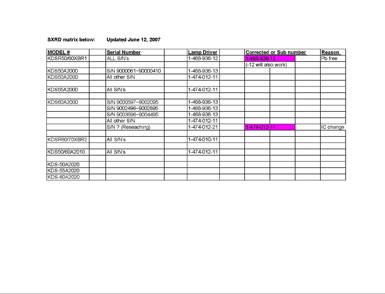
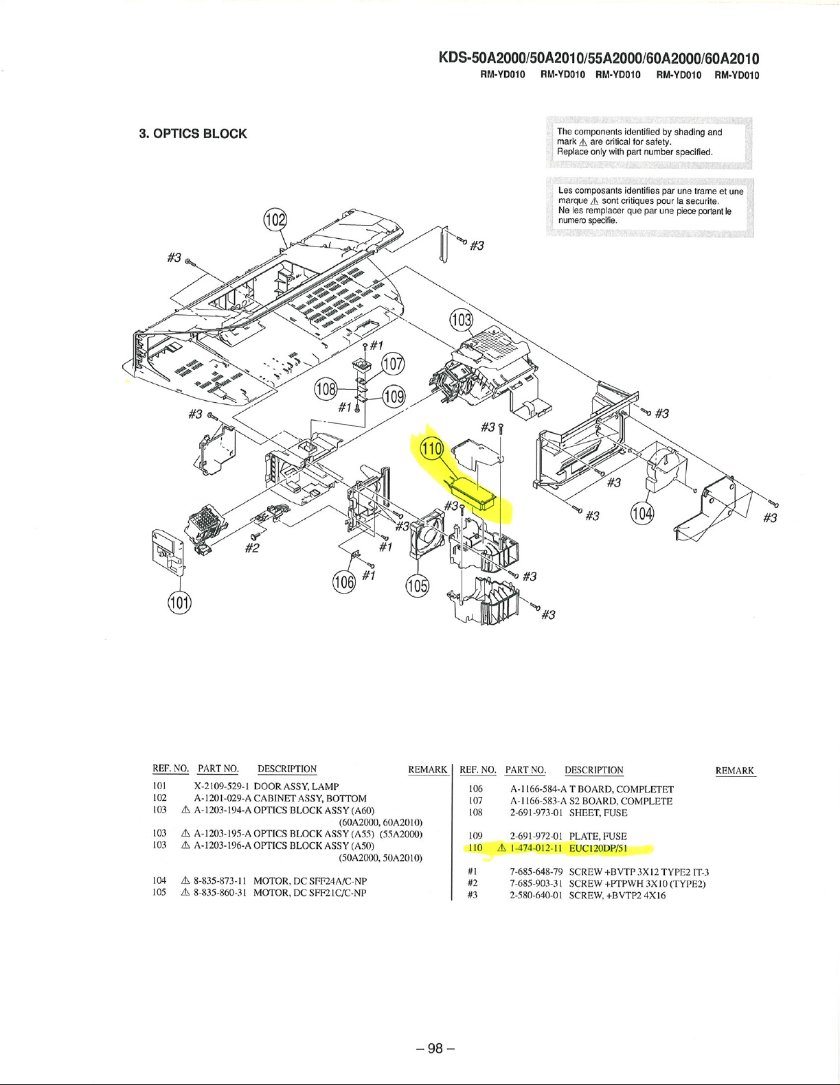

HISTORY
Model Name:
SERVICE MANUAL
Part No. : 9-872-789-02
When clicking an item, it’s detail is displayed.
Date SUPP./CORR. Description of SUP/COR
2006.6 – NEW
2006.7 SUPP.-1 Addition of KDS-50A2010 and 60A2010 Yes
KDS-50A2000/50A2010/55A2000/60A2000/60A2010
Change of
main text
SERVICE MANUAL
SP-3
CHASSIS
MODEL COMMANDER DEST. CHASSIS NO.
–––––– –––––––––––– ––––– –––––––––––
KDS-50A2000
KDS-50A2000
KDS-50A2010
KDS-55A2000
KDS-55A2000
RM-YD010
RM-YD010
RM-YD010
RM-YD010
RM-YD010
USA
CANADA
MEXICO
USA
CANADA
MODEL COMMANDER DEST. CHASSIS NO.
–––––– –––––––––––– ––––– –––––––––––
KDS-60A2000
KDS-60A2000
KDS-60A2010
RM-YD010
RM-YD010
RM-YD010
USA
CANADA
MEXICO
OPEN
KDS-50A2000/50A2010/55A2000/60A2000/60A2010
POWER
LAMP
POWER
TIMER
RM-YD010
SXRD PROJECTION TV

KDS-50A2000/50A2010/55A2000/60A2000/60A2010
K RM-YD010 RM-YD010 RM-YD010 RM-YD010 RM-YD010
Specifications
Te levision system:
NTSC American TV Standard
AT SC (8VSB terrestrial) ATSC compliant 8VSB
QAM on cable ANSI/SCTE 07 2000
Channel coverage:
Terrestrial (analog) 2-69
Cable TV (analog) 1-125
Terrestrial (digital) 2-69
Cable TV (digital) 1-135
Antenna:
75-ohm external terminal for VHF/UHF
Screen size (measured diagonally):
KDS-50A2000/KDS-50A2010: 50 inches
KDS-55A2000: 55 inches
KDS-60A2000/KDS-60A2010: 60 inches
Projection system
3 SXRD panel, 1 lens projection system
SXRD panel
0.61 inch SXRD panel 6,220,800 pixels (2,073,600 × 3)
Projection lens
High performance, large diameter hybrid lens F2.5
Lamp
Ultra High Pressure Lamp , 120W, XL-5200
VIDEO IN 1/2/3:
YPBP
(Component Video) (VIDEO 2 only):
R
Y: 1.0 Vp-p, 75 ohms unbalanced,
P
P
S VIDEO (4-pin mini DIN) (VIDEO 1 only):
VIDEO: 1 Vp-p, 75 ohms unbalanced, sync negative
AUDIO: 500 mVrms (100% modulation)
Signal format: 480i, 480p, 720p, 1080i
Y: 1.0 Vp-p, 75 ohms unbalanced, sync negative
C: 0.286 Vp-p (Burst signal), 75 ohms
Impedance: 47 kilohms
HD/DVD IN 4/5:
(Component Video) :
YPBP
R
Y: 1.0 Vp-p, 75 ohms unbalanced,
P
P
AUDIO: 500 mVrms (100% modulation)
Signal format: 480i, 480p, 720p, 1080i
Impedance: 47 kilohms
HDMI IN 6/7:
HDMI: Video: 480i, 480p, 720p, 1080i, 1080p
AUDIO (for HDMI IN 7):
Audio: Two channel linear PCM 32, 44.1 and
500 mVrms (100% modulation)
Impedance: 47 kilohms
(Does not include CableCARD
functionality)
sync negative
B
: 0.7 Vp-p, 75 ohms
R
: 0.7 Vp-p, 75 ohms
sync negative
B
: 0.7 Vp-p, 75 ohms
R
: 0.7 Vp-p, 75 ohms
48 kHz, 16, 20 and 24 bits
AUDIO OUT:
500 mVrms (100% modulation)
More than 1 Vrms at the maximum volume setting (Variable)
50
0 mVrms (Fixed)
DIGITAL OUT(OPTIVAL):
Optical Digital Audio Output (PCM/Dolby digital)
PC IN 8:
D-sub 15-pin, analog RGB, 0.7 Vp-p, 75 ohms, positive
See the PC Input Signal Reference Chart on page 61
PC AUDIO INPUT:
Stereo mini jack, 0.5 Vrms, 47 kilohm
Speaker:
Full range: 70 × 130 mm (2 × 5 inches) (2)
7
1
/
8
/
8
Speaker output:
12 W + 12 W
Power requirement:
120 V AC, 60 Hz
Power consumption:
In use: 210W
In standby: Less than 0.5W
Dimensions (W/H/D):
KDS-50A2000/KDS-50A2010: 1180 × 839 × 447 mm
KDS-55A2000: 1292 × 913 × 480 mm
KDS-60A2000/KDS-60A2010: 1413 × 988× 514 mm
7
/8 × 36 × 19 inches)
(50
1
/2 × 33 1/8 × 17 5/8 inches)
(46
3
(55
/4 × 39 × 20 1/4 inches)
Mass:
KDS-50A2000/KDS-50A2010: 34 kg (75 lb.)
KDS-55A2000: 38 kg (83 lb. 13 oz.)
KDS-60A2000/KDS-60A2010: 43 kg (94 lb. 13 oz.)
Supplied accessories:
Remote control RM-YD010 (1)
Size AA batteries (2)
Operating Instructions (1)
Quick Setup Guide (1)
Warranty Card (1) (A2000)
Product Registration Card (1) (A2000)
Optional accessories:
TV Stand: SU-RS11M(KDS-50A2000/KDS-50A2010)
SU-RS11X
(KDS-55A2000/KDS-60A2000/KDS-60A2010)
Lamp: XL-5200
Design and specifications are subject to change
without notice.
– 2 –

Replacing the Lamp
The projection lamp, like all lamps, will eventually lose brightness and
functionality, which affects the overall performance of your TV. How long
the lamp maintains its brightness will vary depending upon your usage and
environmental conditions. To maintain the quality of your viewing
experience, Sony recommends that you replace the lamp (1) after
approximately 8,000 hours of use; (2) when the screen becomes dark or the
color looks unusual; (3) when the LAMP LED on the front of the TV blinks;
or (4) when the lamp replacement message appears on the TV screen.
•
•
•
•
•
•
KDS-50A2000/50A2010/55A2000/60A2000/60A2010
K RM-YD010 RM-YD010 RM-YD010 RM-YD010 RM-YD010
WARNING
Electric appliances can cause fire or high temperature, resulting in
injury or death. Be sure to follow the instructions below.
Use a Sony XL-5200 replacement lamp (not supplied) for replacement.
Use of any other lamp may damage the TV.
Do not remove the lamp for any purpose other than replacement. Doing
so may cause injury or fire.
Do not put flammable materials and metal objects inside the lamp
receptacle of the TV after removing the lamp. Doing so may cause fire
or electrical shock. Do not touch the lamp receptacle once the lamp has
been removed.
When the lamp eventually burns out, you may hear a noticeable pop
sound. This is normal and it is inherent to this type of lamp.
In rare instances, the bulb may pop inside the lamp unit, but the lamp
unit is designed to contain all of the broken glass pieces inside the lamp
unit.
This TV’s lamp contains mercury and should be disposed of properly.
Consult your local authorities regarding safe disposal. The material
contained in this lamp are similar to those of a fluorescent lamp, so you
should dispose of it in the same way.
How to Replace the
Lamp
1
Turn off the power on the main unit. Wait several minutes, then unplug
the power cord.
(The cooling fan will continue to operate for about two minutes after
turning the power off.)
2
Wait at least 30 minutes after unplugging the power cord to allow the
lamp to cool down before replacing it. To avoid being burned, do not
touch the lamp receptacle once the lamp has been removed.
(Continued)
– 3 –
KDS-50A2000/50A2010/55A2000/60A2000/60A2010
K RM-YD010 RM-YD010 RM-YD010 RM-YD010 RM-YD010
3 Take th e new lamp out of the box.
Do not touch the glass portion of the new lamp.
•Do not shake the lamp. Vibration can damage the lamp or shorten
its life.
•Avoid touching the front glass of a new lamp or the glass of the
lamp receptacle. This may reduce picture quality or lamp life.
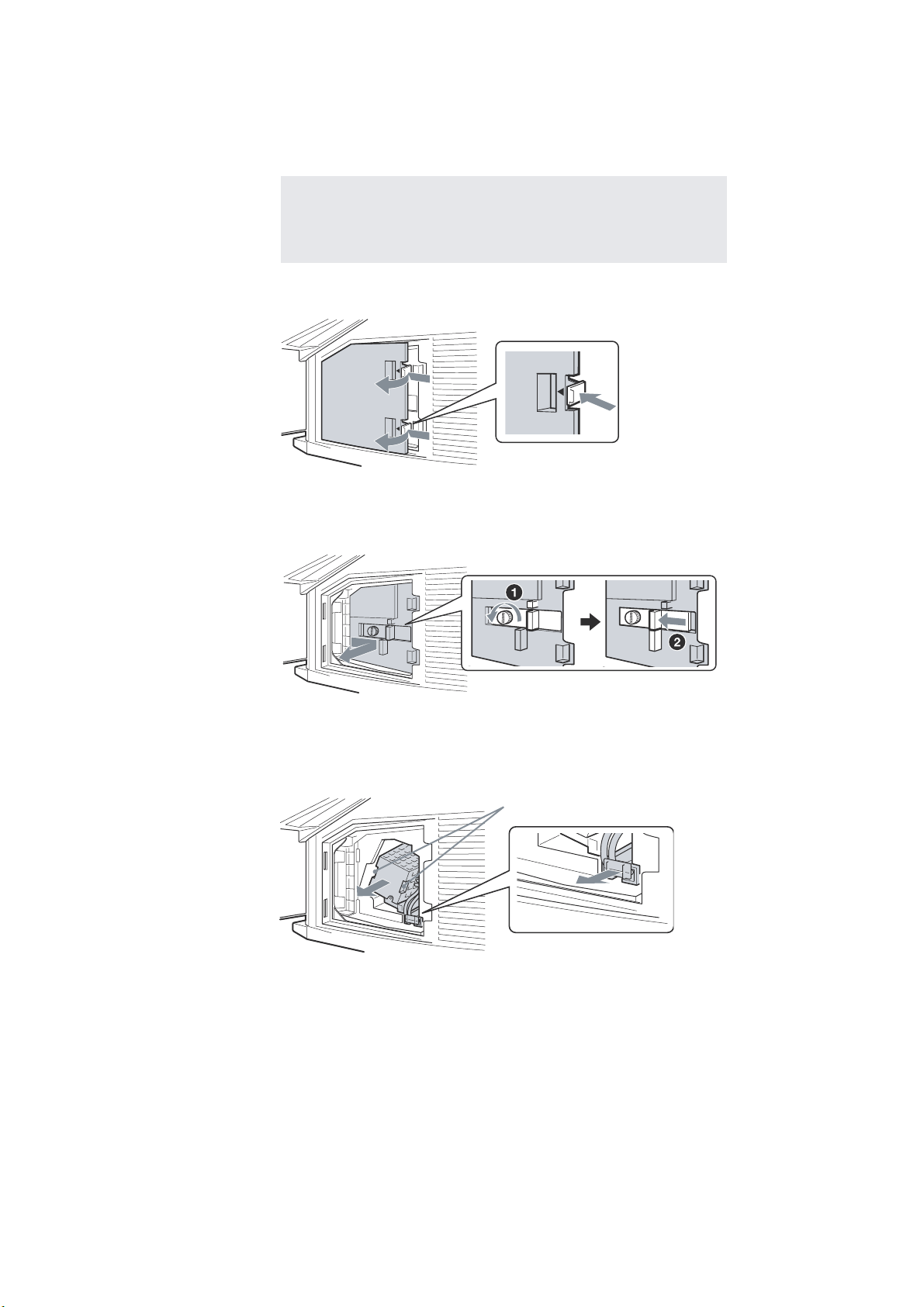
4 Remove the outside lamp cover.
Release the two clamps as shown in the illustration below.
5 Remove the lamp door.
Turn the screw counterclockwise and slide the lever to the left. Remove
the door.
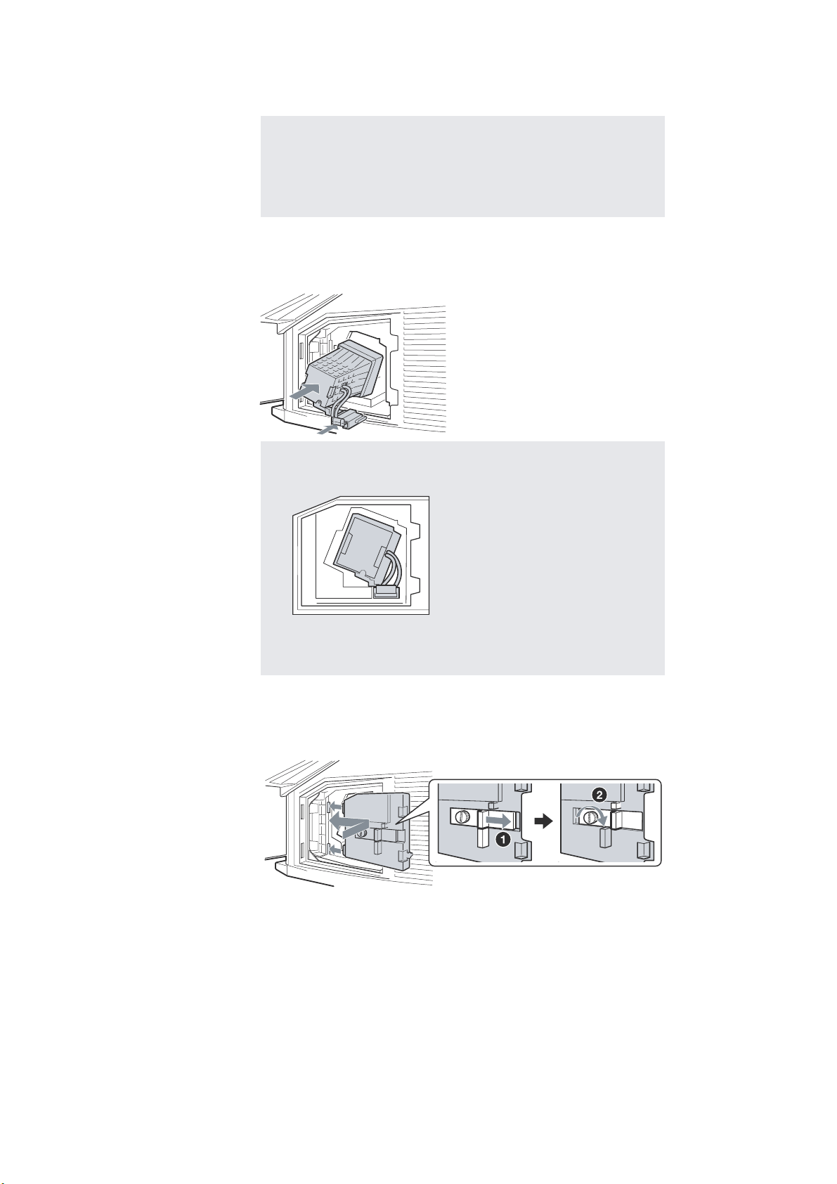
6 Pull out the lamp.
Hold the indented grooves on the top corners of the lamp, as shown in
the illustration, and pull the lamp straight out. If the lamp is hard to
remove, pull the right side of the lamp for additional traction.
Hold this part of the lamp
– 4 –
KDS-50A2000/50A2010/55A2000/60A2000/60A2010
K RM-YD010 RM-YD010 RM-YD010 RM-YD010 RM-YD010
•Do not touch the inside of the lamp compartment.
•The lamp is very hot immediately after use. Never touch the glass
portion of the lamp or the surrounding parts.
•After the used lamp has cooled, place it into the empty box of the
replacement lamp. Never put the used lamp into a plastic bag.
7
Put the new lamp into its place.
Insert the new lamp by pressing the two parts firmly into place as shown
in the illustration. Make sure the lamp is securely mounted into the
compartment. Failure to do so may cause a fire or the screen to go dark.
•The lamp compartment is tilted, as shown in the following
illustration.
•If the lamp is not securely reattached, the self-diagnostic function
may be triggered and the POWER LED blinks three times.
8
Reattach the lamp door.
Replace the door by inserting the two tabs in the slot from the left side.
Slide the lever to the right and then turn the screw clockwise to secure
the door.
– 5 –
(Continued)

KDS-50A2000/50A2010/55A2000/60A2000/60A2010
K RM-YD010 RM-YD010 RM-YD010 RM-YD010 RM-YD010
9
Put the outside lamp cover back in its place.
Replace the cover, inserting it from the left side. Press the two tabs on
the right side to secure the cover.
10
Turn on the TV and set the
settings. This setting is necessary to inform you when the
next lamp replacement is needed.
•Until you set the Lamp Replacement option, a message
announcing that the lamp is at the end of its life will appear every
time you turn on the TV.
•Consult your Sony dealer for a Sony XL-5200 replacement lamp.
•Take great care when replacing the lamp or plugging in/unplugging
the connecting cords. Rough handling may cause the TV to fall,
damaging the TV, the TV stand and the floor.
Lamp Replacement
option in the
Setup
The used lamp
For customers in the United States:
This product contains mercury. Disposal of this product may be regulated if
sold in the United States. For disposal or recycling information, please
contact your local authorities or the Electronics Industries Alliance
(http://www.eiae.org).
•
Do not leave the used lamp near flammable materials or within the
reach of children.
•
Do not pour water onto the used lamp or put any object inside the lamp.
Doing so may cause the lamp to burst.
For replacement lamp information visit:
U. S. residents: http://www.sonystyle.com/tv/
Canadian residents: http://www.sonystyle.ca/tv/
– 6 –

KDS-50A2000/50A2010/55A2000/60A2000/60A2010
Fig. B. Checking for earth ground.
Trouble Light
AC Outlet Box
Ohmmeter
Cold-water Pipe
K RM-YD010 RM-YD010 RM-YD010 RM-YD010 RM-YD010
SAFETY CHECK-OUT
( US model only )
After correcting the original service problem, perfom the follow-
ing safety checks before releasing the set to the customer:
l. Check the area of your repair for unsoldered or poorly-sol-
dered connections. Check the entire board surface for solder
splashes and bridges.
2. Check the interboard wiring to ensure that no wires are
“pinched” or contact high-wattage resistors.
3. Check that all control knobs, shields, covers, ground straps,
and mounting hardware have been replaced. Be absolutely
certain that you have replaced all the insulators.
4. Look for unauthorized replacement parts, particularly transistors, that were installed during a previous repair. Point them
out to the customer and recommend their replacement.
5. Look for parts which, through functioning, show obvious
signs of deterioration. Point them out to the customer and
recom mend their replacement.
6. Check the line cords for cracks and abrasion. Recommend
the replacement of any such line cord to the customer.
7. Check the condition of the monopole antenna (if any). Make
sure the end is not broken off, and has the plastic cap on it.
Point out the danger of impalement on a broken antenna to
the customer, and recommend the antenna’s replacement.
8. Check the B+ and HV to see they are at the values specified.
Make sure your instruments are accurate;be suspicious of
your HV meter if sets always have low HV.
9. Check the antenna temminals, metal trim, “metallized” knobs,
screws, and all other exposed metal parts for AC leakage.
Check leakage as described below.
LEAKAGE TEST
The AC leakage from any exposed metal part to earth ground and
from all exposed metal parts to any exposed metal part having a
return to chassis, must not exceed 0.5mA (500 microampers) . Leakage current can be measured by any one of three methods.
1. A commercial leakage tester, such as the Simpson 229 or
RCA WT-540A. Follow the manufacturers’ instructions to
usc these instruments.
2. A battery-operated AC milliammeter. The Data Precision 245
digital multimeter is suitable for this job.
3. Measuring the voltage drop across a resistor by means of a
VOM or battery-operated AC voltmeter. The “limit” indication is 0.75V, so analog meters must have an accurate lowvoltage scale. The Simpson 250 and Sanwa SH-63Trd are
examples of a passive VOM that is suitable. NearIy all battery operated digital multimeters that have a 2V AC range
are suitable. (See Fig. A)
HOW TO FIND A GOOD EARTH GROUND
A cold-water pipe is guaranteed earth ground;the cover-plate retaining screw on most AC outlet boxes is also at earth ground. If
the retaining screw is to be used as your earth-ground, verify that it
is at ground by measuring the resistance between it and a coldwater pipe with an ohmmeter. The reading should be zero ohms. If
a cold-water pipe is not accessible, connect a 60-l00 watts trouble
light (not a neon lamp) between the hot side of the receptacle and
the retaining screw. Try both slots, if necessary, to locate the hot
side of the line, the lamp should light at normal brilliance if the
screw is at ground potential. (See Fig. B)
Fig. A. Using an AC voltmeter to check AC leakage.
1.5 µ F
To Exposed Metal
Parts on Set
1.5k Ω
Earth Ground
AC
voltmeter
(0.75V)
– 7 –

KDS-50A2000/50A2010/55A2000/60A2000/60A2010
K RM-YD010 RM-YD010 RM-YD010 RM-YD010 RM-YD010
CAUTION
These servicing instructions are for use by qualified service personnel only.
To reduce the risk of electric shock, do not perform any servicing
other than that contained in the operating instructions unless you
are qualified to do so.
WARNING!!
AN ISOLATION TRANSFORMER SHOULD BE USED DURING
ANY SERVICE TO AVOID POSSIBLE SHOCK HAZARD, BECAUSE OF LIVE CHASSIS.
THE CHASSIS OF THIS RECElVER IS DIRECTLY CONNECTED
TO THE AC POWER LINE.
SAFETY-RELATED COMPONENT WARNING!!
COMPONENTS IDENTIFIED BY SHADING AND MARK ! ON THE
SCHEMATIC DIAGRAMS, EXPLODED VIEWS AND IN THE
PARTS LIST ARE CRITICAL TO SAFE OPERATION. REPLACE
THESE COMPONENTS WITH SONY PARTS WHOSE PART NUMBERS APPEAR AS SHOWN IN THIS MANUAL OR IN SUPPLEMENTS PUBLISHED BY SONY. CIRCUIT ADJUSTMENTS THAT
ARE CRITICAL TO SAFE OPERATION ARE IDENTIFIED IN THIS
MANUAL. FOLLOW THESE PROCEDURES WHENEVER CRITICAL COMPONENTS ARE REPLACED OR IMPROPER OPERATION IS SUSPECTED.
ATTENTION!!
AFIN D’EVITER TOUT RISQUE DELECTROCUTION PROVENANT D’UN CHÁSSIS SOUS TENSION, UN TRANSFORMATEUR
D’ISOLEMENT DOIT ETRE UTILISÉ LORS DE TOUT DEPANNAGE.
LE CHÁSSIS DE CE RECEPTEUR EST DIRECTEMENT RACCORDÉ Á L’ALIMENTATION SECTEUR.
ATTENTION AUX COMPOSANTS RELATIFS ÁLA
SÉCURITÉ!!
LES COMPOSANTS IDENTIFIÉS PAR UNE FRAME ET PAR UNE
MAPQUE ! SUR LES SCHÉMAS DE PRINCIPE, LES VUES EXPLOSÉES ET LES LISTES DE PIECES SONT D’UNE IMPORTANCE
CRITIQUE POUR LA SÉCURITÉ DU FONCTIONNEMENT. NE LES
REMPLACER QUE PAR DES COMPOSANTS SONY DONT LE
NUMÉRO DE PIÉCE EST INDIQUÉ DANS LE PRÉSENT MANUEL OU DANS DES SUPPLÉMENTS PUBLIÉS PAR SONY. LES
RÉGLAGES DE CIRCUIT DONT L’IMPORTANCE EST CRITIQUE
POUR LA SÉCURITÉ DU FONCTIONNEMENT SONT IDENTIFIES
DANS LE PRÉSENT MANUEL. SUIVRE CES PROCÉDURES
LORS DE CHAQUE REMPLACEMENT DE COMPOSANTS CRITIQUES, OU LORSQU’UN MAUVAIS FONCTIONNEMENT SUSPECTÉ.
– 8 –

KDS-50A2000/50A2010/55A2000/60A2000/60A2010
K RM-YD010 RM-YD010 RM-YD010 RM-YD010 RM-YD010
TABLE OF CONTENTS
Section Title Page
–––––– –––– ––––
SPECIFICATIONS ....................................................... 2
REPLACING THE LAMP ........................................... 3
1. SELF DIAGNOSIS FUNCTION ..................... 11
2. DISASSEMBLY
2-1. Rear Cover .......................................................... 14
2-2. Chassis Block ..................................................... 15
2-3. Shield ATSC ....................................................... 16
2-4. Terminal Bracket ................................................ 16
2-5. QT Board, QM Board ......................................... 17
2-6. Main Shield ........................................................ 18
2-7. A1, B1, S1 Boards .............................................. 18
2-8. Lamp Fan Unit .................................................... 19
2-9. Power Block ....................................................... 19
2-10. Scirocco Fan ....................................................... 20
2-11. Unit Cover Assembly ......................................... 20
2-12. Optics Block Assembly ...................................... 21
2-13. Screen Frame Block Assembly .......................... 22
2-14. Front Terminal Bracket ...................................... 22
2-15. Mirror Cover Block ............................................ 23
3. ELECTRICAL ADJUSTMENTS
3-1. Picture Distortion Correction Mechanism ............ 24
3-1-1. V-TRAP Correction 1 ................................... 24
3-1-2. V-TRAP Correction 2 ................................... 24
3-1-3. Picture Rotation Correction 1 ....................... 24
3-1-4. Picture Rotation Correction 2 ....................... 24
3-2. Electrical Adjustment by Remote Commander .... 24
3-2-1. Method of Setting the Service Adjustment
Mode ............................................................... 24
3-2-2. Service Mode Adjustment ............................ 24
3-2-3. Memory Write Confirmation Method .......... 25
3-2-4. Adjusting Buttons and Indicator ................... 25
3-3. To Read Lamp and Panel Time ......................... 25
3-4. Test Reset ........................................................... 25
3-5. H/V Center Confirmation and Adjustment ........ 25
Section Title Page
–––––– –––– ––––
4. DIAGRAMS
4-1. Block Diagram (1) .............................................. 26
Block Diagram (2) .............................................. 27
Block Diagram (3) .............................................. 28
Block Diagram (4) .............................................. 29
Block Diagram (5) .............................................. 30
Block Diagram (6) .............................................. 31
Block Diagram (7) .............................................. 32
Block Diagram (8) .............................................. 33
Block Diagram (9) .............................................. 34
Block Diagram (10) ............................................ 35
4-2. Frame Schematic Diagram ................................. 36
4-3. Circuit Boards Location ..................................... 37
4-4. Schematic Diagrams ........................................... 37
(1) Schematic Diagram of A1 (1/6) Board .............. 38
(2) Schematic Diagram of A1 (2/6) Board ............. 39
(3) Schematic Diagram of A1 (3/6) Board ............. 40
(4) Schematic Diagram of A1 (4/6) Board ............. 41
(5) Schematic Diagram of A1 (5/6) Board ............. 42
(6) Schematic Diagram of A1 (6/6) Board .............. 43
(7) Schematic Diagram of B1 (1/11) Board ........... 44
(8) Schematic Diagram of B1 (2/11) Board ........... 45
(9) Schematic Diagram of B1 (3/11) Board ........... 46
(10) Schematic Diagram of B1 (4/11) Board ........... 47
(11) Schematic Diagram of B1 (5/11) Board ............ 48
(12) Schematic Diagram of B1 (6/11) Board ............ 49
(13) Schematic Diagram of B1 (7/11) Board ............ 50
(14) Schematic Diagram of B1 (8/11) Board ........... 51
(15) Schematic Diagram of B1 (9/11) Board ........... 52
(16) Schematic Diagram of B1 (10/11) Board .......... 53
(17) Schematic Diagram of B1 (11/11) Board ......... 54
(18) Schematic Diagram of C (1/11) Board ............. 55
(19) Schematic Diagram of C (2/11) Board ............. 56
(20) Schematic Diagram of C (3/11) Board ............. 57
(21) Schematic Diagram of C (4/11) Board ............. 58
(22) Schematic Diagram of C (5/11) Board .............. 59
(23) Schematic Diagram of C (6/11) Board .............. 60
(24) Schematic Diagram of C (7/11) Board .............. 61
(25) Schematic Diagram of C (8/11) Board ............. 62
(26) Schematic Diagram of C (9/11) Board ............. 63
(27) Schematic Diagram of C (10/11) Board ............ 64
(28) Schematic Diagram of C (11/11) Board ............ 65
(29) Schematic Diagram of G (1/2) Board ................ 66
(30) Schematic Diagram of G (2/2) Board ............... 67
– 9 –

KDS-50A2000/50A2010/55A2000/60A2000/60A2010
K RM-YD010 RM-YD010 RM-YD010 RM-YD010 RM-YD010
Section Title Page
–––––– –––– ––––
(31) Schematic Diagram of H1 Board ...................... 68
(32) Schematic Diagram of H2 Board ....................... 69
(33) Schematic Diagram of H3 Board ....................... 70
(34) Schematic Diagram of QM (1/6) Board ............ 71
(35) Schematic Diagram of QM (2/6) Board ............ 72
(36) Schematic Diagram of QM (3/6) Board ............ 73
(37) Schematic Diagram of QM (4/6) Board ............ 74
(38) Schematic Diagram of QM (5/6) Board ............ 75
(39) Schematic Diagram of QM (6/6) Board ............ 76
(40) Schematic Diagram of QT Board ...................... 77
(41) Schematic Diagram of S1, S2 Boards ................ 78
(42) Schematic Diagram of T Board ......................... 79
4-5. Printed Wiring Boards ........................................ 80
(1) A1 Board (Side A).............................................. 80
(2) A1 Board (Side B) .............................................. 81
(3) B1 Board (Side A) .............................................. 82
(4) B1 Board (Side B) .............................................. 83
(5) C Board (Side A) ................................................ 84
(6) C Board (Side B) ................................................ 85
(7) G Board (Side A) ................................................ 86
(8) G Board (Side B) ................................................ 87
(9) H1, H2 Boards .................................................... 88
(10) H3 Board ............................................................. 89
(11) QM Board (Side A) ............................................ 90
(12) QM Board (Side B) ............................................ 91
(11) QT Board (Side A) ............................................. 92
(12) QT Board (Side B) ............................................. 93
(13) S1, S2, T Boards ................................................. 94
4-6. Semiconductors .................................................. 95
Section Title Page
–––––– –––– ––––
5. EXPLODED VIEWS
5-1. Screen, Covers .................................................... 96
5-2. Chassis Assembly ............................................... 97
5-3. Optics Block ....................................................... 98
6. ELECTRICAL PARTS LIST
• A1 Board ................................................................... 99
• B1 Board ................................................................... 112
• C Board ..................................................................... 122
• G Board ..................................................................... 133
• H1 Board ................................................................... 137
• H2 Board ................................................................... 137
• H3 Board ................................................................... 137
• QM Board ................................................................. 138
• QT Board .................................................................. 143
• S1 Board .................................................................... 144
• S2 Board .................................................................... 144
• T Board ..................................................................... 144
– 10 –

KDS-50A2000/50A2010/55A2000/60A2000/60A2010
r
K RM-YD010 RM-YD010 RM-YD010 RM-YD010 RM-YD010
SECTION 1
SELF DIAGNOSIS FUNCTION
1. Summary of Self-Diagnosis Function
-This device includes a self-diagnosis function.
-Incaseofabnormalities, the POWER indicatorautomatically blinks. It is possible to
predict the abnormality location by the number of blinks. The Instruction
describes blinking of thePOWER indicator.
-Ifthe symptom is not reproduced sometimes in case of a malfunction, there is recording of
whether a malfunction was generated or not. Operate the remote command to confirm the
matter on the screen and to predict the location of the abnormality.
2. Diagnosis Items and Prediction of Malfunction Location
-When a malfunction occurs the POWER indicator only blinks for one of the
following diagnosis items. In case of two or more malfunctions, the item which first
occurred blinks. If the malfunctions occurred simultaneously, the item with the lowe
blink count blinks first.
-The screen display displays the results regarding all the diagnosis items listed below.
Thedisplay "0" means that no malfunctions occurred.
Manual
Number of times
Diagnosis Item
Temp. over
La
mp cover
Fan error
Lamp driver
Power error 6 times
Audio prot 7 times
Power
Device error
OVP
POWER
indicator blinks
2 times
3
times
4 times
5 times
times
8
9 times
Probable Cause
Location
-The periphery of lamp
heats up abnormally
-L
amp cover is not
attached securely.
power is not
-Fan1
supplied.
-Fan connector is not
attached securely.
-Lampdriver is faulty. - No picture/No sound
- D5V is not
supplied.
- Speaker line is shorted.
over voltage.
is
-7V
Temperature sensors,
Bus decoder ICs
(IC1700, 1800, 1900,
5066, 2305)
IC6402
Defected symptoms
-Nopicture/No sound
-Nopicture/No sound
-Nopicture/No sound
-Nopicture/No sound
-Nopicture/No sound
-Nopicture/No sound
-No picture
Lamp error L
AMP-LEDflashes - No picture/No sound
-Lampfor the light
source burns out.
– 11 –
KDS-50A2000/50A2010/55A2000/60A2000/60A2010
m
r
m
m
K RM-YD010 RM-YD010 RM-YD010 RM-YD010 RM-YD010
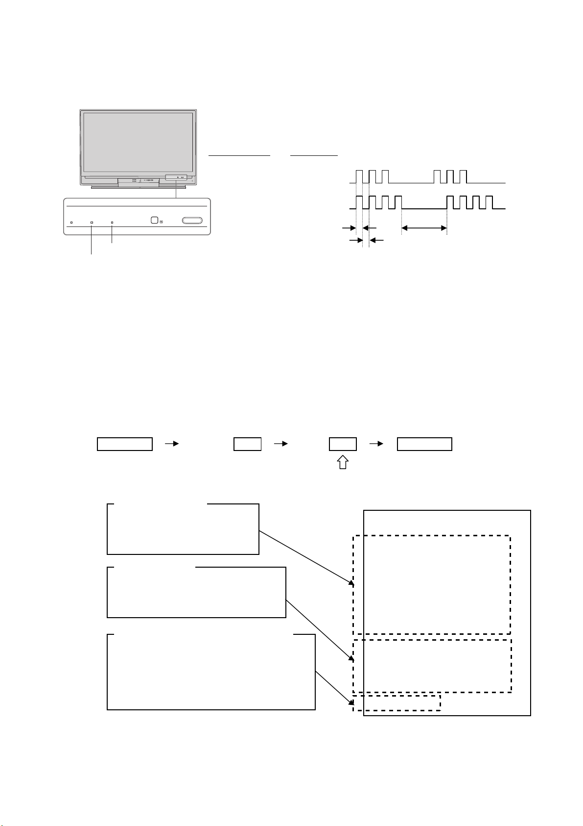
3. Blinking count display ofPOWER/STANDBY indicator
-One blink is not used for self-diagnosis.
-Example
Diagnosis ite
LEDblinks
OPEN
POWER
LAMP
POWER
TIMER
Lamp cove
3 times
Fan 4 times
R
LAMP
TIMER
POWER indicator
LAMP indicator
POWER
POWE
LEDON:0.3sec
LEDOFF : 0.3sec
LED OFF
3.0sec
-Release of POWER/STANDBY indicator blinking
The POWER/STANDBY indicatorblinking display is released by removing the plug fro
the power or leaving for 2 minutes.
4. Self-diagnosis screen displays
-Incases of malfunctions where it is not possible to determine the symptom such as when
the power goes off occasionally or when the screen disappears occasionally, there is a
screen display on whether the malfunction occurred or not in the past (and whether the
detection circuit operated or not) in order to allow confirmation.
<Screen Display Method>
-Quickly press the remote command button in the following order from the standby state.
DISPLAY 5 - POWER
ChannelVol
Be aware that thisdiffers fro
service mode (Vol +).
Error information
002 : LED blink times
SELF CHECK
TEMP : Panel Temp Error
001 : Error count (Max 255)
002 : TEMP 001
003 : L_COVER 000
Reboot counter
102 : Error number
TVM_WDT : Reboot micro
002 : WDT count (Max 255)
Boot count and total power on time
Display rule
12345-67890 : alternately display
(ex.) Boot Count 13579 times
Total power on time 24680 hours
Each max is 99999
004 : FAN 003
005 : L_DRIVER 000
006 : POWER 000
007 : AUDIO 000
008 : P_OVP 000
009 : DEVICE 000
101 : DTT_WDT 000
102 : TVM_WDT 002
103 : WEM_WDT 000
104 : DEM_WDT 000
12345-67890
* The boot count is increased at all power on timing.
(AC Off ->Power On, Main SW Off -> Power On, Standby -> Power On)
* The total power on time is written to NVM at 1 time per a hour.
the method of entering the
– 12 –

KDS-50A2000/50A2010/55A2000/60A2000/60A2010
-The results display is not automatically cleared. In case of repairs and after repairs, chec
k
the self-diagnosis screen and be sure to return the results display to "0".
-Ifthe results display is not returned to "0" it will not be possible to judge a new malfunction
after completing repairs.
<Method of Clearing Results Display>
1. Power off (Set to the standby mode)
2. Channel Vol
3. Channel
<Method of Ending Self-Diagnosis Screen>
-When ending the self-diagnosis screen completely, turn the power switch OFF on the
remote commander or the main unit.
5. Self-Diagnosis function operation
8ENTER
DISPLAY 5 - POWER
2:Temp over When the inside temperature sensed with IC3150, IC3200 and IC2000
mounted on S1 board, S2 board and C board respectively exceed
the threshold, DEM (Display Engine u-com) detects it and makes
turn off the lamp.
3:Lamp cover When the lamp cover is opened or harness from T board is off, DEM detects it
and makes turn off the lamp
4:FAN error When any FAN is stopping or harness is not connected correctly,
DEM detects it and makes turn off the lamp
5:Lamp Driver When the ballast is not working with high voltage, DEM detects it and makes
turn off the lamp
6:Power error When the voltage converted on 5V regulated from 11V is low, TVM
(TV u-com) detects it and makes turn off the lamp.
7:Audio When DC is appeared by audio amp failure at speaker line, DEM detects it
and makes turn off the lamp.
8:Power-OVP When the output voltage from 7V is abnormally high, TVM detects
it and makes turn off the lamp.
9:Device error When the temperature sensor and bus decoder ICs do not return ACK on IIC
bus to DEM, DEM detects it and makes turn off the lamp.
LAMP : Lamp When the lamp is broken, DEM detects it.
K RM-YD010 RM-YD010 RM-YD010 RM-YD010 RM-YD010
– 13 –
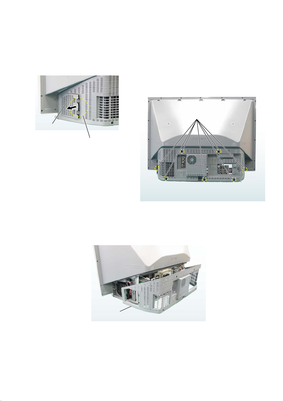
2-1. REAR COVER
3
2
1 Pull the claw
Lamp door
7 screws (+BVTP2 4x16)
Rear cover
KDS-50A2000/50A2010/55A2000/60A2000/60A2010
K RM-YD010 RM-YD010 RM-YD010 RM-YD010 RM-YD010
SECTION 2
DISASSEMBLY
– 14 –
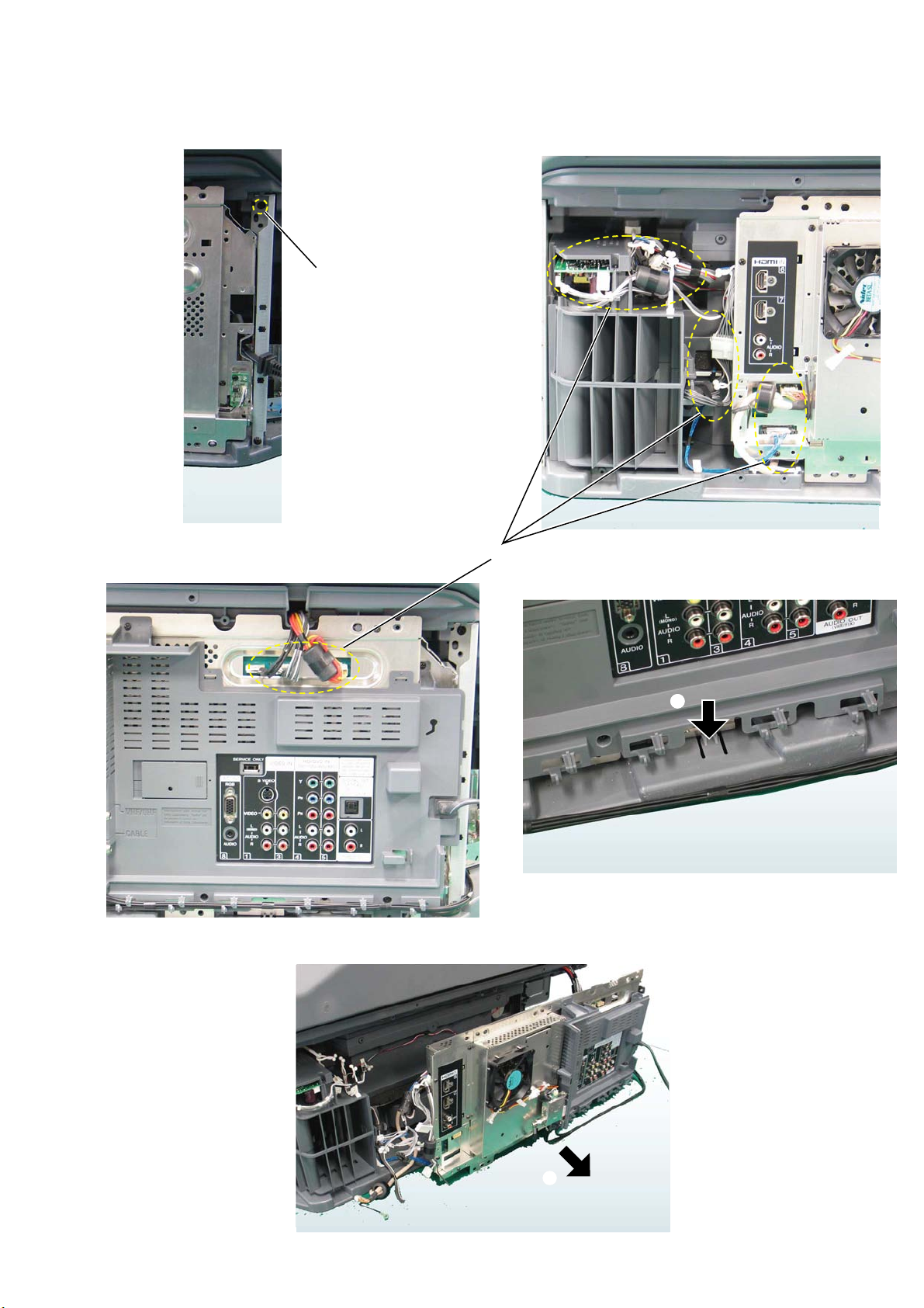
2-2. CHASSIS BLOCK
2 Screw (+BVTP2 4x16)
1 Connectors
3
3
KDS-50A2000/50A2010/55A2000/60A2000/60A2010
K RM-YD010 RM-YD010 RM-YD010 RM-YD010 RM-YD010
– 15 –
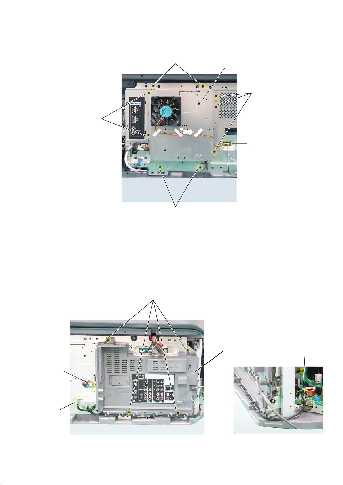
2-3. SHIELD ATSC
KDS-50A2000/50A2010/55A2000/60A2000/60A2010
K RM-YD010 RM-YD010 RM-YD010 RM-YD010 RM-YD010
2 2 screws (+BVST 3x6)
2 2 screws (+BVST 3x6)
2 2 screws (+BVST 3x6)
Shield ATSC
2 3 screws (+BVST 3x6)
1 Connector
2-4. TERMINAL BRANCKET
1 Connector
1 F cable
2 4 screws (+BVST 3x6)
Te r minal bracket
1 2 connectors
– 16 –
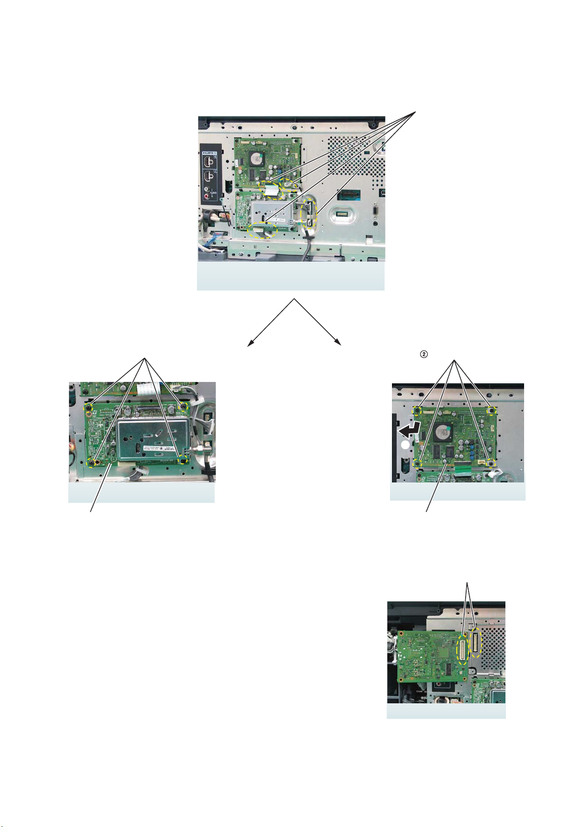
2-5. QT BOARD, QM BOARD
KDS-50A2000/50A2010/55A2000/60A2000/60A2010
K RM-YD010 RM-YD010 RM-YD010 RM-YD010 RM-YD010
1 6 connectors
2 4 screws (+BVST 3x6)
3 QT board
4 screws (+BVST 3x6)
3
4 QM board
Be careful about the connector connected
between QM board and A1 board.
– 17 –
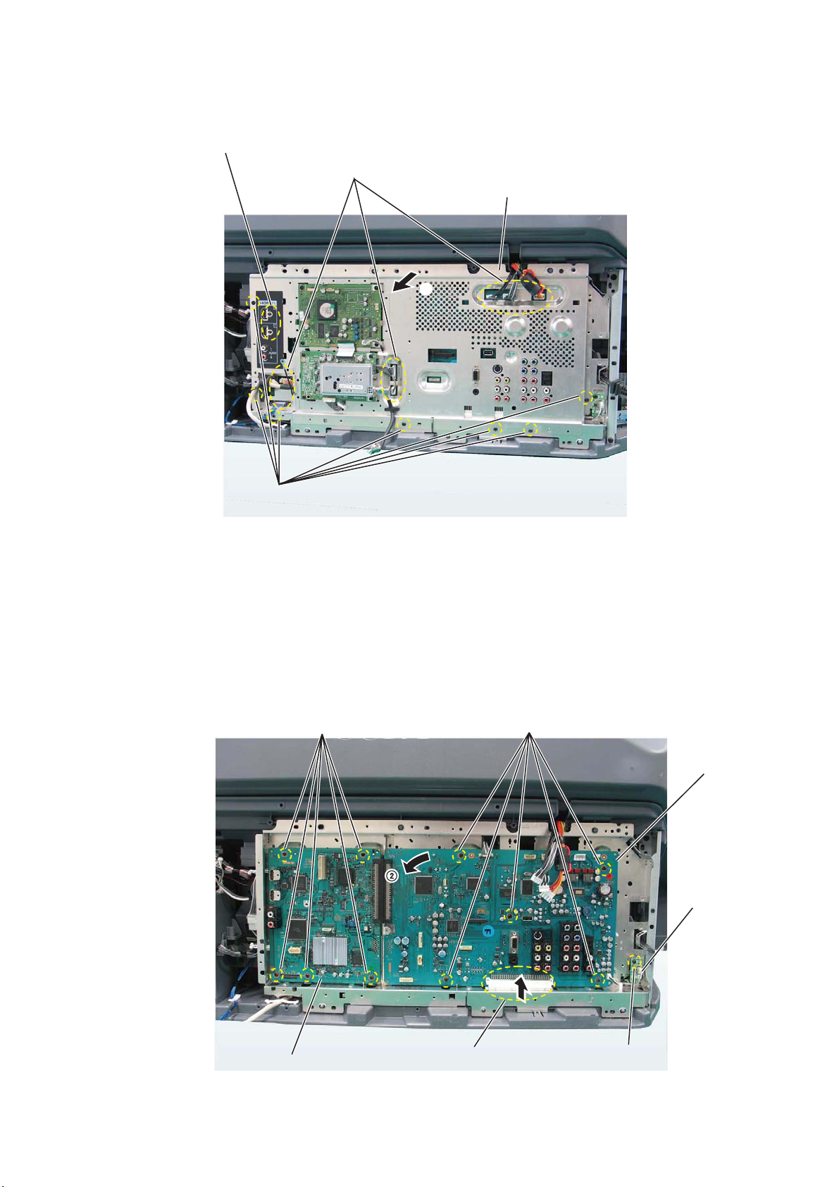
2-6. MAIN SHIELD
2 screws (+PSW M 3x8)
3
KDS-50A2000/50A2010/55A2000/60A2000/60A2010
K RM-YD010 RM-YD010 RM-YD010 RM-YD010 RM-YD010
1 7 connectors
Main shield
4
2 7 screws (+BVST 3x6)
2-7. A1, B1, S1 BOARD
1 5 screws (+BVST 3x6)
1 5 screws (+BVST 3x6)
A1 board
S1 board
5
B1 board
3
– 18 –
Connector
4 Screw (+BVST 3x6)
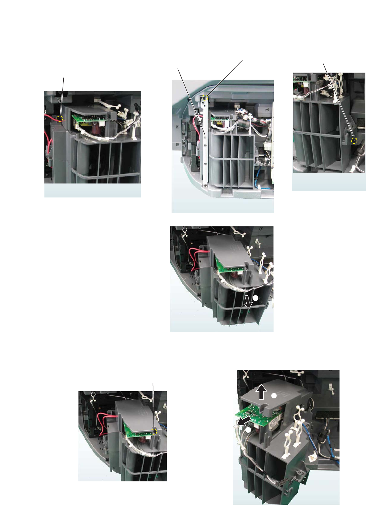
2-8. LAMP FAN UNIT
Screw (+BVTP2 4x16)
3
KDS-50A2000/50A2010/55A2000/60A2000/60A2010
K RM-YD010 RM-YD010 RM-YD010 RM-YD010 RM-YD010
2
Side stay (R)
1 Screw (+BVTP2 4x16)
Screw (+BVTP2 4x16)
3
2-9. POWER BLOCK
4
1 Screw (+BVTP2 4x16)
2
3
– 19 –
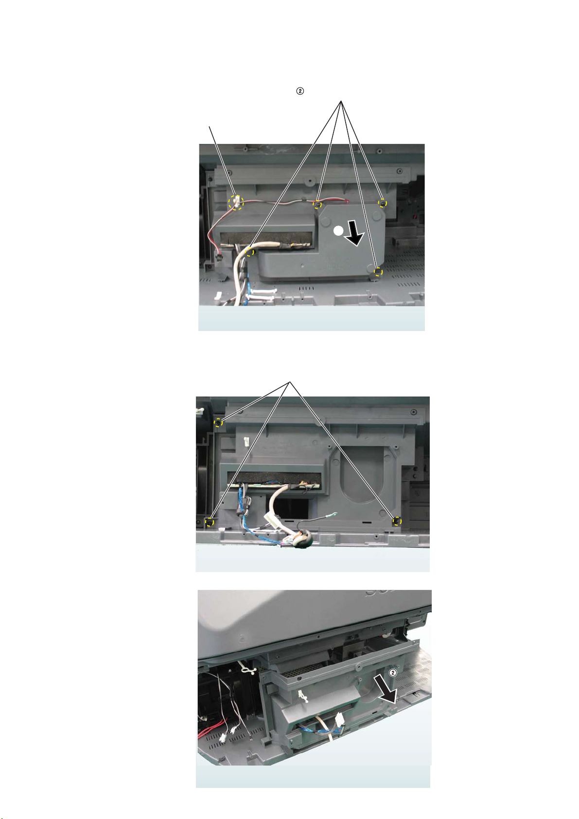
2-10. SCIROCCO FAN
KDS-50A2000/50A2010/55A2000/60A2000/60A2010
K RM-YD010 RM-YD010 RM-YD010 RM-YD010 RM-YD010
4 screws (+BVTP2 4x16)
1
3
2-11. UNIT COVER ASSEMBLY
3 screws (+BVTP2 4x16)
1
– 20 –
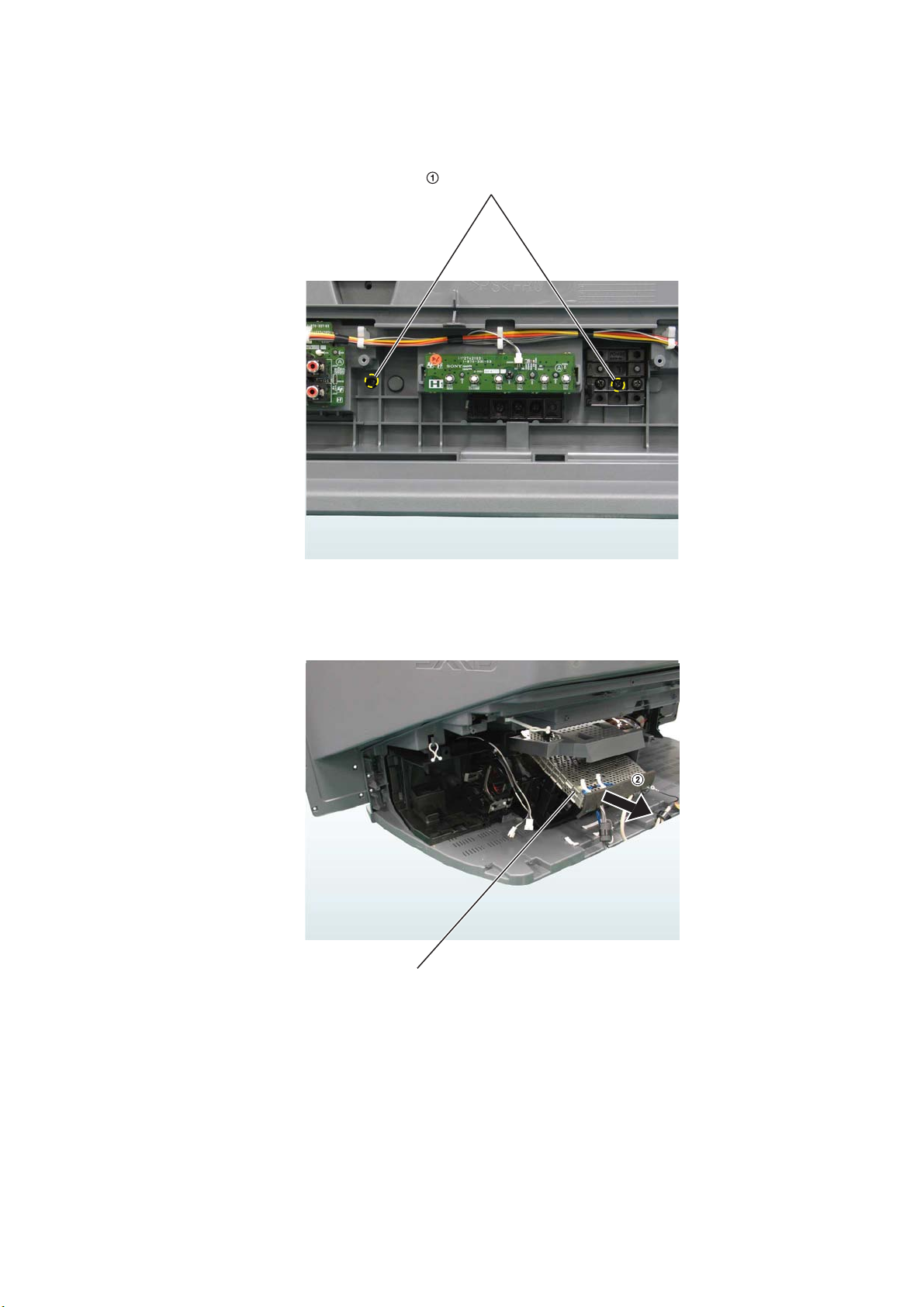
2-12. OPTICS BLOCK ASSEMBLY
KDS-50A2000/50A2010/55A2000/60A2000/60A2010
K RM-YD010 RM-YD010 RM-YD010 RM-YD010 RM-YD010
2 screws (+BVTP2 4x16)
Optics block assembly
– 21 –
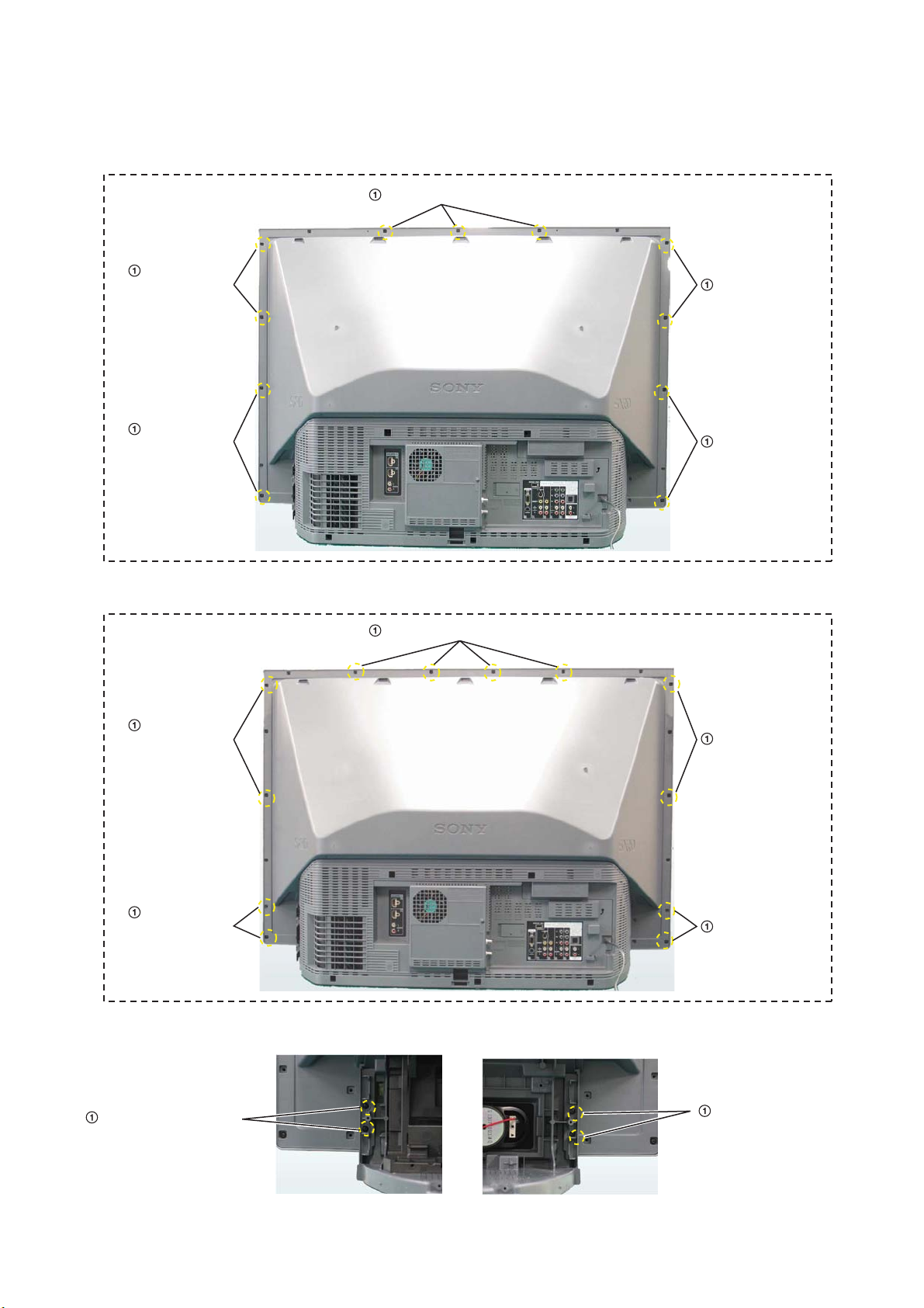
2-13. SCREEN FRAME BLOCK ASSEMBLY
50A2000
3 screws (+BVTP2 4x16)
KDS-50A2000/50A2010/55A2000/60A2000/60A2010
K RM-YD010 RM-YD010 RM-YD010 RM-YD010 RM-YD010
2 screws
(+BVTP2 4x16)
2 screws
(+BVTP2 4x16)
55A2000/60A2000
2 screws
(+BVTP2 4x16)
2 screws
(+BVTP2 4x16)
4 screws (+BVTP2 4x16)
2 screws
(+BVTP2 4x16)
2 screws
(+BVTP2 4x16)
2 screws (+BVTP2 4x16)
2 screws
(+BVTP2 4x16)
2 screws
(+BVTP2 4x16)
2 screws (+BVTP2 4x16)
– 22 –
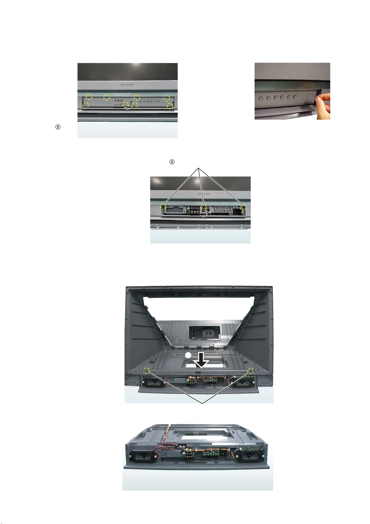
2-14. FRONT TERMINAL BRACKET
Remove 7 claws of front terminal bracket by inserting the
pin 5 to 10mm to the 7 square holes on the edge of front
teminal bracket.
At this time, pay attention not to scratch front terminal bracket.
KDS-50A2000/50A2010/55A2000/60A2000/60A2010
K RM-YD010 RM-YD010 RM-YD010 RM-YD010 RM-YD010
2 screws (+BVTP2 4x16)
2-15. MIRROR COVER BLOCK
2
2 screws (+BVTP2 4x16)
1
– 23 –

K RM-YD010 RM-YD010 RM-YD010 RM-YD010 RM-YD010
SECTION 3
ELECTRICAL ADJUSTMENTS
3-1. PICTURE DISTORTION CORRECTION
MECHANISM
3-1-1. V-TRAP Correctin 1
In case of movimg the V spacer by changing the position of center screw on the V spacer 2 to 1, the picture center goes down and
square to trapezoid as shown in figure.
3-1-2. V-TRAP Correctin 2
In case of movimg the V spacer by changing the position of center screw on the V spacer 2 to 3, the picture center goes up and
square to trapezoid as shown in figure.
KDS-50A2000/50A2010/55A2000/60A2000/60A2010
3-2. ELECTRICAL ADJUSTMENT BY REMOTE
COMMANDER
By using remote commander (RM-YD010), all circuit adjust-
ments can be made.
NOTE : Test Equipment Required.
1. Pattern Generator (with component outputs)
2. Oscilloscope
3. Digital multimeter
3-2-1. Method of Setting the Service Adjustment
Mode
3-1-3. Picture Rotation Correctin 1
In case of movimg the R spacer by changing the position of
screws on the R spacer B to A, the picture rotates clockwise as
shown in figure.
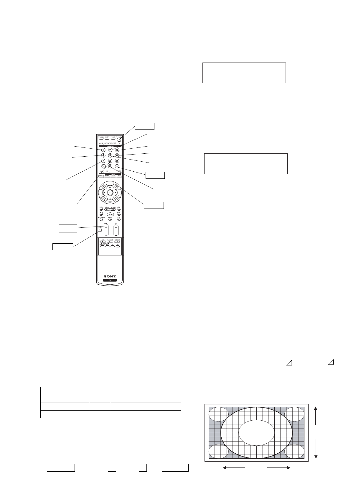
1. Standby mode. (Power off)
2. DISPLAY t 5 t VOL (+) t TV POWER
on the remote commander.
(Press each button within a second.)
The following service screen will appear.
Category Name
Item Name
Item No.
VERSION 0 0 SERVICE
VER TVMICRO
Item Name Input Signal
F/A : xxxxxxxx
CBA : xxxxxxxx
Category Name
D9671-1 0 0 G
I2CSCAL
96H 28DEG
9CH 24DEG
LCD PJ ENGINE VER.10.00B
Item No.
03/10/07 732B
Data
Mode
Data
3-1-4. Picture Rotation Correctin 2
In case of movimg the R spacer by changing the position of
screws on the R spacer B to C, the picture rotates counterclock-
wise as shown in figure.
<LCD PROJECTOR ENGINE>
3-2-2. Service Mode Adjustment
1. The SCREEN displays the item being adjusted.
2. Press “1” or “4” on the remote commander to select the
adjustment item.
3. Press “3” or “6” on the remote commander to change the data.
4. Press “2” or “5” on the remote commander to select the category.
5. If you want to recover the latest values press “-” then
“[ENTER]” to read the memory.
6. Press “[MUTING]” then “[ENTER]” to write into memory.
7. Turn power off.
– 24 –
KDS-50A2000/50A2010/55A2000/60A2000/60A2010
K RM-YD010 RM-YD010 RM-YD010 RM-YD010 RM-YD010
<Method of setting the shipping condition>
1. Service Adjustment mode.
2. Press “8” then “[ENTER]”
3. Wait until appearing “ Initial Setup” display.
4. Disconnect AC plug and connect again to change factory reset
condition completely.
3-2-3. Memory Write Confirmation Method
1. After adjustment, turn power off with the remote commander.
2. Turn power on and set to service mode.
3. Call the adjusted items again and confirm they were adjusted.
3-2-4. Adjusting Buttons and Indicator
POWER
Adjustment category
up
Adjustment item
up
Adjustment item
down
Initialize data
(Not stored)
User control goes
to the standerd state
(Shipping Conditions)
VOL +
MUTING
Data up
Data down
Adjustment category
down
ENTER
Read data from
NVM
DISPLAY
2. Press the “JUMP ” key [3 times].
You’ll get into DE-micro service menu .
3. Press “2 ” key [12 times] to show the following display .
Example
DEM SERVICE
13 Timer
1 LAMP TIMER 14
This screen reads
“Total lamp time is 14 hours”.
To reset lamp time,
press “1 ” to set the reset.
press “3 ” , “MUTE ” and “ENTER ” keys in sequence.
WRI-EXE(Red Character) is momentarily displayed and
LampTM will be reset to “0 ”.
4. Press “ 1 ” key [7 times].
Example
DEM SERVICE
13 Timer
2 LAMP TIMER 0
<To get out of the Service menu>
The Service menu is cleared by turning off the set with a remote
commander or the power switch .
3-4. Test Reset
The user settings can be reset to the factory default condition as
follows.
1. Press “TEST “ and “RESET “ key in sequence when the set is ON
.
The LAMP,TIMER and POWER LED light and the picture is
muted.
After about 5 seconds the LAMP and TIMER LED go off,
and the color of POWER LED changes from amber to green.
After another 10 seconds the reset is completed and the initial
set-up display appears.
RM-YD010
FUNCTION OF KEYS ON COMMANDER
• 1 : Changes adjustment item. (item No. moves up)
• 4 : Changes adjustment item. (item No. moves down)
• 2 : Changes adjustment category.
(category moves up)
• 5 : Changes adjustment category.
(category moves down)
• 3 : Changes data value. (up)
• 6 : Changes data value. (down)
Commander Function
Button Mode Description
[MUTING] + [ENTER] WRITE Writes data to NVM.
- + [ENTER] READ Reads data from NVM.
8 + [ENTER] RESET Set the shipping condition.
3-3. To read Lamp and Panel time
The lamp and panel time of the set are displayed as follows .
<Enter the service mode>
1. Press the keys of the remote commander in rapid sequence as follows , when the set is in standby mode.
3-5. H/V Center Confirmation and Adjust-
ment
Please check the picture horizontal/vertical center after the re-
placement of the following parts .
• Optical block
• Top assembly
1, Check H/V center with 480i monoscope signal in “Full “
mode .
2, If the center is shifted , adjust it with the following service items .
Please record the steps shifted as
CXD9713 .
DEM/TG H_CENT (for H center)
V_CENT (for V center)
DFD 16 and
V_SENT
DISPLAY t Channel 5 t Vol + t POWER
– 25 –
H_CENT
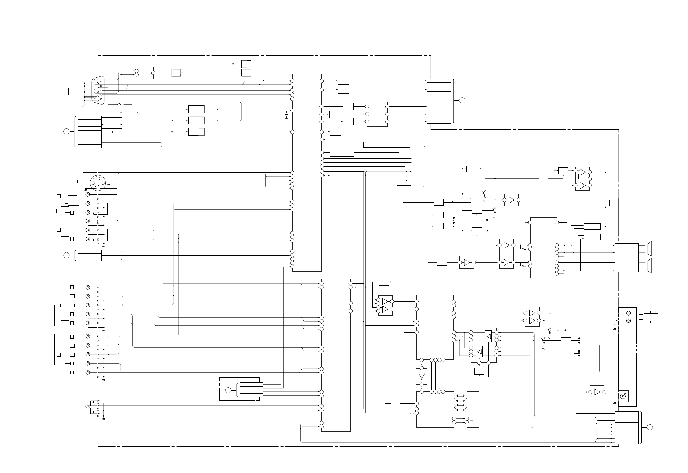
4-1. BLOCK DIAGRAM (1)
SECTION 4
DIAGRAMS
KDS-50A2000/50A2010/55A2000/60A2000/60A2010
K RM-YD010 RM-YD010 RM-YD010 RM-YD010 RM-YD010
VIDEO IN
HD/DVD IN
QT BOARD
CN7803
1
AUDIO
3
AUDIO
H3 BOARD
4
AUDIO
5
AUDIO
TO
A
M
TO
CN3100
CN8570
PC IN
RGB
S VIDEO
VIDEO
L (MONO)
R
VIDEO
L (MONO)
R
Y
P
B
P
R
L
R
Y
P
B
P
R
L
R
J8570
PC IN
AUDIO
CN8303
CN8006 (1/2)
TB8300
V
L
R
V
L
R
CN8301
J8401
1 2
GRN
BLU
RED
WHT
RED
GRN
BLU
RED
WHT
RED
IC8570
EEPROM
SCL
6
WP
7
SDA
TU_V_OUT
AFT_MAIN
AGC
SCL_3.3V
SDA_3.3V
AU_L3
AU_R3
PC_B
PC_G
PC_R
AU_L1
AU_R1
5
D5V
AUDIO R
TO/FROM 2/2
VIDEO
K
AUDIO L
K
K
SCL
PC_V
PC_H
SDA
Vcc
F8570
9AFT_OUT
14AGC_MUTE
12TU_SCL
13TU_SDA
10TU_V_OUT
TV_M_L_IN
7TU_L_OUT
TV_M_R_IN
5TU_R_OUT
Y1
CY
C1
43
S1
V1
V3
CR2
1COMP2_CR
CB2
3COMP2_CB
Y2
5COMP2_Y
Y4
CB4
CR4
AU_L4
AU_R4
Y5
CB5
CR5
AU_L5
AU_R5
PC_AU_R
PC_AU_L
K
AUDIO L/R
Q8570
SW
Q8308, 8309
BUFFER
Q8317-8319
BUFFER
Q8313, 8315
BUFFER
Y4
CB4
CR4
Y5
CB5
CR5
D5V
WRT_PRT
MAIN_H_SYNC
V_DET
AUDIO L/R
K
TO
H3 BOARD
CN3101
N
Q8314
CLAMP
Q8316
CLAMP
TO/FROM
2/2
CN8001 (1/2)
VIDEO
K
15V2_V
14COMP_DET
17V2_L
19V2_R
V3
S1
V1
Y1
C1
V2
COMP_DET
V2_INPUT_L2
V2_INPUT_R2
X8300
4MHz
PC_V
PC_H
37
IN4_V
38
IN4_H
92
B_IN14
93
G_IN14
94
R_IN14
49
EXT_CLK/XTAL
1
IN2_CV
21
CV3
116
S1_4
119
CV/CR/R_IN9
118
Y/Y/G_IN9
117
C/CB/B_IN9
2
Y/Y/G_IN8
1
C/CB/B_IN8
3
C/CB/B_IN8
6
Y/Y/G_IN7
5
C/CB/B_IN7
7
C/CB/B_IN7
11
Y/Y/G_IN6
9
C/CB/B_IN6
10
C/CB/B_IN6
23
CV2
8
S1_3
IC8301
VIDEO SW
CV/YOUT1_2
COUT1_2
C/CR/R_OUT1_1
CV/Y/G_OUT1_1
C/CB/B_OUT1_1
SYNC_OUT1
SYNC_IN1
CVOUT3
SEL_HOUT1
SEL_VOUT1
PS_HVCS
TV_M_L_IN
TV_M_R_IN
AU_L1
AU_R1
AU_L3
AU_R3
AU_L4
AU_R4
AU_L5
AU_R5
DVI_L
DVI_R
AUDIO L
SC1_IN_L
SC1_IN_R
I2C_CL
I2CDA
RESETQ
AUDIO_CLOCK_OUTPCLK
74
2
4
11
SCL
SDA
A27
A28
A29
A30
A31
TO/FROM
2/2
K
K
IC9304
59 13 8 11
IC9305
CN8304 (1/4)
MAIN_CV/Y
MAIN_C
MAIN_CR/R
MAIN_Y/G
MAIN_CB/B
Q9608
SW
Q9604
SW
Q9610
SW
Q9818
AMP
AUDIO R
SP_OUT_L
SP_OUT_R
SC2_OUT_L
SC2_OUT_R
DSP
I2S_DA_IN3
I2S_WS3
I2S_CL3
I2S-DEL_IN
I2S-DEL_OUT9I2S-DEL_CL10I2S-DEL_WS
8
11
IISM_IN
BIT_CLK
IISM_OUT
DELAY
TO
B1 BOARD
B
CN4000
Q9816
11V AP +B
D9815
D9816
IO0
ı
IO7
LR_CLK
A0
ı
A16
FWR
FRD
IC9807
5
28
27
34
33
22
20
19
292229
Q9803
AMP
IC9306
I/O1
I/O8
A16
22
REG.
SW
A0
14
16
18
RAM
ı
ı
3
5
7
WE
OE
Q9806
Q9810
SW
Q9601
SW
AUDIO L
7
AUDIO R
IC9400
I2S SELECTOR
19 1
Q9300
SW
D9814
K
K
IC9809
MUTE AMP
3
Q9809
5
3
IC9802
AMP
FE_BCK
6
FE_LRCK
4
FE_DATA
2
HDMI_BCK
17
HDMI_LRCK
15
HDMI_DATA
13
HDMI/DTT_SW
FROM 2/2
A1(1/2)
VIDEO/AUDIO SWITCH,
( )
Q9820
SW
1
IC9804
AP
STBY/MUTE
6
7
1
IC9308
5
3
IN1
8
CP1O
7
19
IN2
20
CP2O
AMP
7
1
OUTA1
OUTA1
OUTB1
OUTB1
OUTB2
OUTB2
OUTA2
OUTA2
Q9311
A9V
VREF
Q9310
14
48
47
43
41
38
36
32
31
AUDIO AMP
IC9803
D9316
Q9314
AMP
5
+
3
D9311
SW
D9317
Q9602
SW
HDMI_INT
LINE_MUTE
Q9819
AMP
7
6
1
Q9811, 9813
DC DET
Q9812, 9814
DC DET
IC9301
3
AMP
FE_BCK
FE_LRCK
FE_DATA
HDMI_BCK
HDMI_LRCK
HDMI_DATA
DVI_L
DVI_R
Q9815
SW
AUDIO L
AUDIO L
AUDIO R
AUDIO R
VAR_L
VAR_R
FROM 2/2
4
K
K
K
K
A49
A43
B43
A44
B59
A60
B60
A54
A55
CN9800
39
34
42
37 R+
TB8301
CN8304 (2/4)
FE_SPDIF
FE_ABCK
FE_ALRCK
FE_ADATA
HDMI_ABCK
HDMI_ALRCK
HDMI_ADATA
DVI_LR_IN_L
DVI_LR_IN_R
L+
L-
R-
L
R
L
AUDIO OUT
(VAR/FIX)
R
DIGITAL OUT
(OPTICAL)
TO
B1 BOARD
CN4000
SP_L
SP_R
C
1
7
Q9316
B_12V
AUDIO L
AUDIO R
SW
CV/Y
K
C
K
CR/R
K
Y/G
K
CB/B
K
SP_PROT
DATA_SLICER_MAIN
VSW_HS
VSW_VS
PC_SYNC_DET
I2C_5V
SP_MUTE
AMP_RST
PFC_DET
56
K
57
K
2
3
21
IC9303
18
2
3
IN1_L
IN1_R
IN5_L
IN5_R
IN6_L
IN6_R
IN7_L
IN7_R
IN8_L
IN8_R
IN4_L
IN4_R
IN3_R
IN3_L
IN9_L
IN9_R
BUFFER
IC9602
AUDIO SW
Q8300
BUFFER
Q8301
BUFFER
Q8305
BUFFER
Q8307
Q8306
BUFFER
Q8311
BUFFER
Q8327, 8328, 8330
BUFFER
SCL_5V
SDA_5V
CLK-1
DAT-1
LOUT1
ROUT1
31
32
39
37
AUDIO L
AUDIO R
IC8302
BUFFER
OUT3
IN+3
10
5
12
K
K
7
OUT1
IN+1
1
1
OUT2
IN+2
Q9614
AMP
IC9606
INV.
+
3
-
2
+
5
-
6
DLY_RST RST
FROM 2/2
90
89
85
83
81
40
41
71
53
54
50
SCL
60
SDA
59
1
2
13
14
16
17
19
20
22
23
10
11
8
7
25
26
– 26 –
KDS-50A2000/50A2010/55A2000/60A2000/60A2010
K RM-YD010 RM-YD010 RM-YD010 RM-YD010 RM-YD010
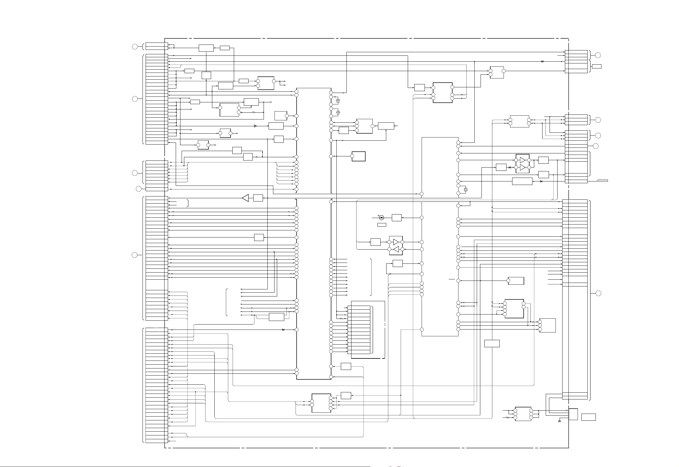
BLOCK DIAGRAM (2)
TO
QM BOARD
CN7306
TO
G BOARD
CN6902
TO
H2 BOARD
CN3050
H1 BOARD
FROM
CN3000
S
F
G
E
TO
B1 BOARD
CN4000
H
TO
JIG
CN8803
CN8805
FAN_DRV
A9V
FAN_ERR
LAMP_EX_FAN (FAN1)
PANEL_FAN (FAN3)
11V
11V
11V
11V
11V
11V
REC_ON
AC_RLY
STBY_5V
6.5V
6.5V
6.5V
6.5V
6.5V
D3.3V
6.5V
6.5V
16.5V
16.5V
16.5V
PFC_DET
PANEL_FAN_CONT
CN8001 (2/2)
SIRCS
P_ON
POW_LED
STBY_LED
LAMP_LED
P_MUTE_LED
TIMER_LED
KEY
CN8304 (3/4)
MUTE2
PC_V_SYNC
H_SYNC
DL_MODE
SCL_IFP_TVM
SDA_IFP_TVM
UART_TXD_IFP
UART_RXD_IFP
BE_RST
SET_ON
FE_RST
UART_TX_FE
UART_RX_FE
WRT_PRT
HDMI_RST
HDMI_INT
CCDM_H
INPUT_CE
INPUT_SEL
SCL_HDMI
SDA_HDMI
BOOT_MODE
I_USBDPLS
I_USBCONNECT
I_USBDMNS
TXD_IFP_LOG
RXD_IFP_LOG
UART_LOG_TX_FE
UART_LOG_RX_FE
CN8004
TV_BINT
E_BINT
SCL_TV
SDA_TV
SCL_IFP
SDA_IFP
SCL_DEM_100K
SDA_DEM_100K
SCL_DEM_400K
SDA_DEM_400K
IFP_BOOTMODE
TVM_TXD
TVM_RXD
DTT_TXD
DTT_RXD
DEM_TXD
DEM_RXD
RESET (DE)
SCK (DE)
FLASH_WRITE (DE)
SYNCHRO_MODE (DE)
IFP_UDP
IFP_UDM
IFP_VBUS
IFP_TXD
IFP_RXD
RST_M
SYNCHRO_MODE_M
FLASH_WRITE_M
TU_V_OUT
110.5V
210.5V
B32
A12
B31
FAN1
A30
FAN3
C30
A15
B15
C15
A16
B16
C16
A24
B24
A26
A20
B20
C20
A21
B21
A33
C21
C22
A28
B28
C28
B24
A29
7
5
9
11
13
15
17
20
A16
B31
A32
A25
A33
A34
A37
A38
B37
B41
B45
A47
A48
B49
A52
B53
B55
A58
A59
A50
A51
BOOT_MODE
B34
A39
IFP_VBUS
B39
A40
A41
A42
A45
LOG_RXD
A46
3
4
5
6
7
8
9
10
11
12
BOOT_MODE
14
15
16
17
LOG_RXD
18
DEM_TXD
19
DEM_RXD
20
23
24
FLASH_WRITE_DE
25
SYNCHRO_MODE_DE
26
27
28
29
31
32
35
37
38
39
IC8001
VSW_HS
VSW_VS
IFP_UDP
IFP_UDM
IFP_TXD
IFP_RXD
LOG_TXD
SCL_5V
SDA_5V
SCL_IFP
SDA_IFP
LOG_TXD
SCK_DE
IFP_UDM
IFP_TXD
IFP_RXD
IFP_TXD
IFP_RXD
TU_V_OUT
FL8808
3.3V REG.
FROM 1/2
A9V
11V
STBY_5V
F8800
7V
16.5V
Q8801
10.5V REG.
Q8802
SW.
IC8805
SW. REG. CONT.
IC8000
1.8V REG.
I
SCL_DAC
SDA_DAC
F8801
Q8804, 8816
SW.
72
CTL/SS
I
STBY3.3V
O
TO/FROM 1/2
E_BINT
SCL_JIG
SDA_JIG
JIG_RESET
OUT
INV
O
Q8012
MUTE2
PFC_DET
WRT_PRT
HDMI_INT
AFT_MAIN
SCL_3.3V
SDA_3.3V
I2C_S
SW
AGC
F8802
5
STBY1.8V
IC8006
4
Q8819
3.3V REG.
Q8011
SW
CN8801
11
LAMP TXD
LAMP_RXD
A26
A17
A18
A15
B15
B16
B17
A19
A20
A21
A22
A23
A24
B23
B25
B26
A1, A2
A3, A4
A7-9
B7-9
A10-13
A35
A36
7
2
3
1
3
4
1
3
4
5
7
9
11
13
ANTSW_MAIN
D5V
FAN4_PROT
FAN4_POW
CN8003
D3.3V
SDA_E
SCL_E
CN8000
D3.3V
SDA_E
SCL_E
LAMP_COVER
FLAG
LAMP_ON
LAMP_POWER
HV_DET
CN8304 (4/4)
IFP_VSYNC
SCL_SENSE
SDA_SENXE
PANEL_ON
ROOK_RST
MUTE
NVM_WP2
SCL_E
SDA_E
IRIS_CTRL
IRIS_FB
SCL_IFP_DEM
SDA_IFP_DEM
LVDS _PD_DEM
COM_RST
DE_BUSY
16.5V->D5V
A9V
7V
D3.3V
FE_USB_PB
FE_USB_NB
VBUS
DD+
GND
CN8305
USB
SERVICE
ONLY
FAN_DRV
SCL_SENSE
SDA_SENSE
Q8021
SW
D5V
D3.3V
FAN4_POW
3
IIC-BUS REPEATER
2
IC8504
4OUT
IC8573
GATE
2B
6
1B
2
2C
3
7
1C
IC8009
SCLB
SCLA
SDAB
SDAA3
IC8007
AMP
5
3
Q8024, 8025, 8027
SW
RESET
2A
5
1A
1
IC8304
REG.
2
3
4
7
6
7
1
8
7
6
PFC_DET
LEVEL SHIFT
1
4
IC8802
FAN4 REG.
Q8505
IC8801
Vin
On Off Cont
SCL_5V
SDA_5V
Vout
D3.3V
Q8812, 8813
LEVEL SHIFT
4
IC8008
SW
Q8034
Q8015
5V REG.
RESET
OUT
SW
SIRCS
P_ON
PWR_LED
STBY_LED
LAMP_LED
PMUTE_LED
TIMER_LED
V5V
D5V
4
IC8003
BE MICRO
134
O_BE_ON
133
O_AC_RLY
128
I_LB_ERR
127
I_D_OVP
127
I_AC_DET
91
I_WAKE
86
I_SIRCS
103
I_POWER_KEY
117
O_PWR_LED
118
O_STBY_LED
119
O_LAMP_LED
120
O_PMUTE_LED
121
O_TIMER_LED
37
I_KEY
55
O_DL_MODE
108
IO_IIC_SCL4
110
IO_IIC_SDA4
84
O_UART_TXI
88
I_UART_RXI
47
O_BE_RESET
134
O_BE_ON
113
O_FE_RST
112
O_UART_TX2
111
I_UART_RX2
130
O_PC_HDMI_WP
53
O_HDMI_RST
98
I_HDMI_PC_INT
2
MAIN_H
132
O_HDMI_CE
51
O_HDMI_SEL
78
IO_IIC_SCLK1
I_PC_SYNC_DET
79
IO_IIC_SDA1
O_LINE_MUTE
39
I_AFT_MAIN
45
O_AGC_ATT/O_AGC_MUTE
105
IO_IIC_SCL2
106
IO_IIC_SDA2
44
I_BINT
81
O_UART_TXD
80
I_UART_RXD
I_SYNCHRO_MODE_M
SCL_JIG
6
SDA_JIG
2
O_ANT_M
I_OSC
O_OSC
SUB_CLK_0
SUB_CLK-1
IO_IIC_SDA3
IO_IIC_SCL3
O_NVM_WP
TRSTX
I_RESET
I_VBLK
I_MAIN_HIN
I_V_DET
I_SP_PROT
DATASLICERMAIN
O_AMP_RST
O_DLY_MUTE
O_SP_MUTE
O_HDMI_DTT_SW
O_DLY_RST
BREAK
ICD3
ICD2
ICD1
ICD0
ICS2
ICS1
ICS0
ICLK
MD2
IC8573
GATE
2B
2A
1A
1B
54
57
59
93
95
109
107
129
61
75
97
89
48
149
29
85
138
144
147
148
150
152
63
70
69
68
67
66
65
64
62
73
50
32C
5
1
71C
X8002
10.135MHz
X8001
32.768kHz
Q8006
SW
PANEL_FAN_CONT
PFC_DET
MAIN_H_SYNC
V_DET
SP_PROT
DATA_SLICER_MAIN
PC_SYNC_DET
AMP_RST
DLY_MUTE
LINE_MUTE
SP_MUTE
HDMI/DTT_SW
DLY_RST
STBY
1
3.3V
2
3
4
5
6
7
8
9
10
11
12
14 ICLK
Q8014
SW
SYNCHRO_MODE_M
Q8506
SW
IC8004
NVM
5DAT
6CLK
7
WP
IC8005
RESET
4RST
LAMP TXD
LAMP_RXD
CN8002
UVCC
XTRST
XRSTIN
XINIT
BREAK
ICD3
ICD2
ICD1
ICD0
ICS2
ICS1
ICS0
FLASH_WRITE_M
D3.3V
8VCC
Q8578
SW
TO/FROM
CHECK
D8583
TIMER
1/2
FOR
Q8032, 8033
B+ SW
DAC _I2C
UVCC
Q8578
SW
6
2
5
3
Q8503
SW
FLASH_WRITE_DE
DEM_RXD
DEM_TXD
SCK_DE
SYNCHRO_MODE_DE
E_BINT
Q8700
SW
SDA_DAC
SCL_DAC
1
5
2
Q8034
SW
Q8007
SW
CH_NVM_WP
46
TIMER_LED
118
PD_SENB
32
SIO_SOT3
33
MD0
89
MD2
87
SIO_SIN0
11
SIO_SOT0
12
SIO_SCK0
17
SYNCHRO_MODE
22
104
B_INT
IC8804
FAN CONTROL
6
DAC1
9
SW2
14
SDA
3
DAC3
15
SCL
5
DAC2
IC8505
DE MICRO
FANERR
LAMP_COVER
LAMP_PROT
LAMP_ON
LAMP_MODE
LAMP_MODE
X1
X0
INT_V
PANEL_ON
D_DEV_RST
PIC_MUTE
NVM_WP2
IRIS_PPG
IRIS_FB
I2C_SCL0
I2C_SDA0
PANEL_PD
DE_BUSY
RESET
I2C_SDA1
I2C_SCL1
BUS_SW0
I2C_SDA2
I2C_SCL2
NVM_WP1
A1 (2/2)
FAN1
FAN3
92
63
83
86
84
84
107
X8500
6MHz
108
25
93
50
51
35
69
41
27
28
55
68
90
65
64
91
67
66
99
JIG_RESET
DAC_I2C
(BE MICRO, DE MICRO, CONNECTOR I/F))
D8811
D3.3V
Q8023
SW
Q8022
SW
IFP_VS
SCL_SENSE
SDA_SENSE
SCL_IFP
SDA_IFP
D5V
A9V
7V
D3.3V
IC8506
5SDA2A
6SCL2A
7
WP
D5V
FAN1_POW
NVM
ANTENNA
I
SWITCH
FAN4
TO
S1 BOARD
CN3150
J
TO
S2 BOARD
CN3200
K
TO
T BOARD
L
CN3250
TO
LAMP DRIVER
HV DETECT CABLE
TO
B1 BOARD
CN4000
D
TO
– 27 –
 Loading...