

Sony KDL-70R520A, KDL-60R551A, KDL-50R555A, KDL-70R550A, KDL-70R551A Service Manual
...
HISTORY INFORMATION FOR THE FOLLOWING MANUAL:
Self Diagnosis
SERVICE MANUAL
MODEL COMMANDER DESTINATION
KDL-50R550A RM-YD094 US / Canada
KDL-50R550A RM-YD094 Mexico / Latin America
KDL-50R555A RM-YD095 Chile / Peru / Venezuela
KDL-50R557A RM-YD095 Colombia
KDL-60R520A RM-YD096 US / Canada
KDL-60R550A RM-YD094 US / Canada
KDL-60R550A RM-YD094 Mexico / Latin America
KDL-60R551A RM-YD094 Mexico / Latin America
KDL-60R555A RM-YD094 Chile / Peru / Venezuela
RB1FK
Segments: BL
CHASSIS
KDL-60R557A RM-YD094 Colombia
KDL-70R520A RM-YD096 US
KDL-70R550A RM-YD094 US / Canada
KDL-70R550A RM-YD094 Mexico / Latin America
KDL-70R551A RM-YD094 Mexico / Latin America
KDL-70R555A RM-YD094 Chile / Peru / Venezuela
KDL-70R557A RM-YD094 Colombia
Supported model
ORIGINAL MANUAL ISSUE DATE: 12/2013
REVISION DATE SUBJECT
12/9/2013 Original Manual Release Date
9-883-557-51
LCD DIGITAL COLOR TV

Chassis: RB1FK, BL
TABLE OF CONTENTS
SECTION TITLE PAGE
SECTION 1: DIAGRAMS ................................................................................................................................................................................................... 7
1-1. Printed Circuit Boards and Schematic Diagrams Information .................................................................................................................... 7
1-2. Circuit Boards Location .................................................................................................................................................................................. 8
1-3. Connector Diagrams ........................................................................................................................................................................................ 9
For 50” Models Only ........................................................................................................................................................................................9
For 60” & 70” Models Only ............................................................................................................................................................................ 10
1-4. Main Board (A Board) .................................................................................................................................................................................... 11
A Board Component Side .............................................................................................................................................................................. 11
A Board Conductor Side ................................................................................................................................................................................12
A Board Schematic ........................................................................................................................................................................................13
SECTION 2: POWER SUPPLY BOARD (G BOARD) ..................................................................................................................................................... 39
G Board Component Side .............................................................................................................................................................................39
G4 Schematic for 50” Models Only ..............................................................................................................................................................40
GE60 Schematic for 60” Models Only .......................................................................................................................................................... 41
GE70 Schematic for 70” Models Only .......................................................................................................................................................... 43
SECTION 3: IR BOARD (H BOARD) ..............................................................................................................................................................................46
H Board Component Side ..............................................................................................................................................................................46
H Board Conductor Side ...............................................................................................................................................................................46
H Board Schematic ........................................................................................................................................................................................47
SECTION 4: ELECTRICAL PART LIST .......................................................................................................................................................................... 48
APPENDIX A: ENCRYPTION KEY COMPONENTS ..................................................................................................................................................... A-1
Chassis: RB1FK, BL 2
Chassis: RB1FK, BL
CAUTIONS AND WARNINGS
CAUTION
. To reduce the risk of electric shock, do not
WARNING!!
An isolation transformer should be used during any service to avoid possible shock hazard, in case of live chassis.
!
SAFETY-RELATED COMPONENT WARNING!!
shading and
NOTE: Do not modify the original design without obtaining written permission from the manufacturer or you will void the
original parts and labor warranty.
!
mark on the schematic diagrams and the parts list. It is essential that these critical parts be replaced only
ATTENTION!!
ainsi.
ALERTE!!
lors de tout dépannage.
!
ATTENTION AUX COMPOSANTS
RELATIFS A LA SECURITE!!
les listes de pieces sont d’une importance critique pour la securite du fonctionnement. Ne les remplacer que par des
composants Sony dont le numero de piece est indique dans le present manuel ou dans des supplements publies par
present manuel. Suivre ces procedures lors de chaque remplacement de composants critiques, ou lorsqu’un mauvais
fonctionnement suspecte.
Chassis: RB1FK, BL 3
!
sur les schemas de principe, les vues explosees et
Chassis: RB1FK, BL
USE CAUTION WHEN HANDLING THE LCD PANEL
When repairing the LCD panel, be sure you are grounded by using a wrist band.
When installing the LCD panel on a wall, the LCD panel must be secured using the 4 mounting holes on the rear
cover.
To avoid damaging the LCD panel:
1. Do not press on the panel or frame edge to avoid the risk of electric shock.
2. Do not scratch or press on the panel with any sharp objects.
3. Do not leave the module in high temperatures or in areas of high humidity for an extended period of time.
4. Do not expose the LCD panel to direct sunlight.
5. Avoid contact with water. It may cause a short circuit within the module.
6. Disconnect the AC power when replacing the backlight (CCFL) or inverter circuit.
(High voltage occurs at the inverter circuit at 650Vrms.)
7. Always clean the LCD panel with a soft cloth material.
8. Use care when handling the wires or connectors of
the inverter circuit. Damaging the wires may cause a
short.
9. Protect the panel from ESD to avoid damaging the
electronic circuit (C-MOS).
10. During the repair, DO NOT leave the Power On for
more than 1 hour while the TV is face down on a
cloth.
CLEANING THE LCD PANEL
CAUTION: When cleaning the TV, be sure to unplug the power cord to avoid any chance of electric shock.
Clean the cabinet of the TV with a dry soft cloth.
Wipe the LCD screen gently with a soft cloth.
Stubborn stains may be removed with a cloth slightly moistened with a solution of mild soap and warm water.
If using a chemically pretreated cloth, please follow the instruction provided on the package.
Never use strong solvents such as a thinner, alcohol or benzine for cleaning.
Periodic vacuuming of the ventilation openings is recommended to ensure proper ventilation.
Do Not use paper towels, any type of abrasive pad, rags, rubber or vinyl materials to clean the screen. Using
these materials could easily scratch the screen which may result in permanent damage.
Do Not use any cleaning product containing alkaline/acid cleaner, scouring powder, or volatile solvent, such as
alcohol, ammonia, benzine, thinner or insecticide. Using any of these harsh cleaners may result in permanent
damage to the screen.
Do Not spray water or detergent directly onto the TV screen . If liquid drips into the bottom of the screen it may
cause a failure.
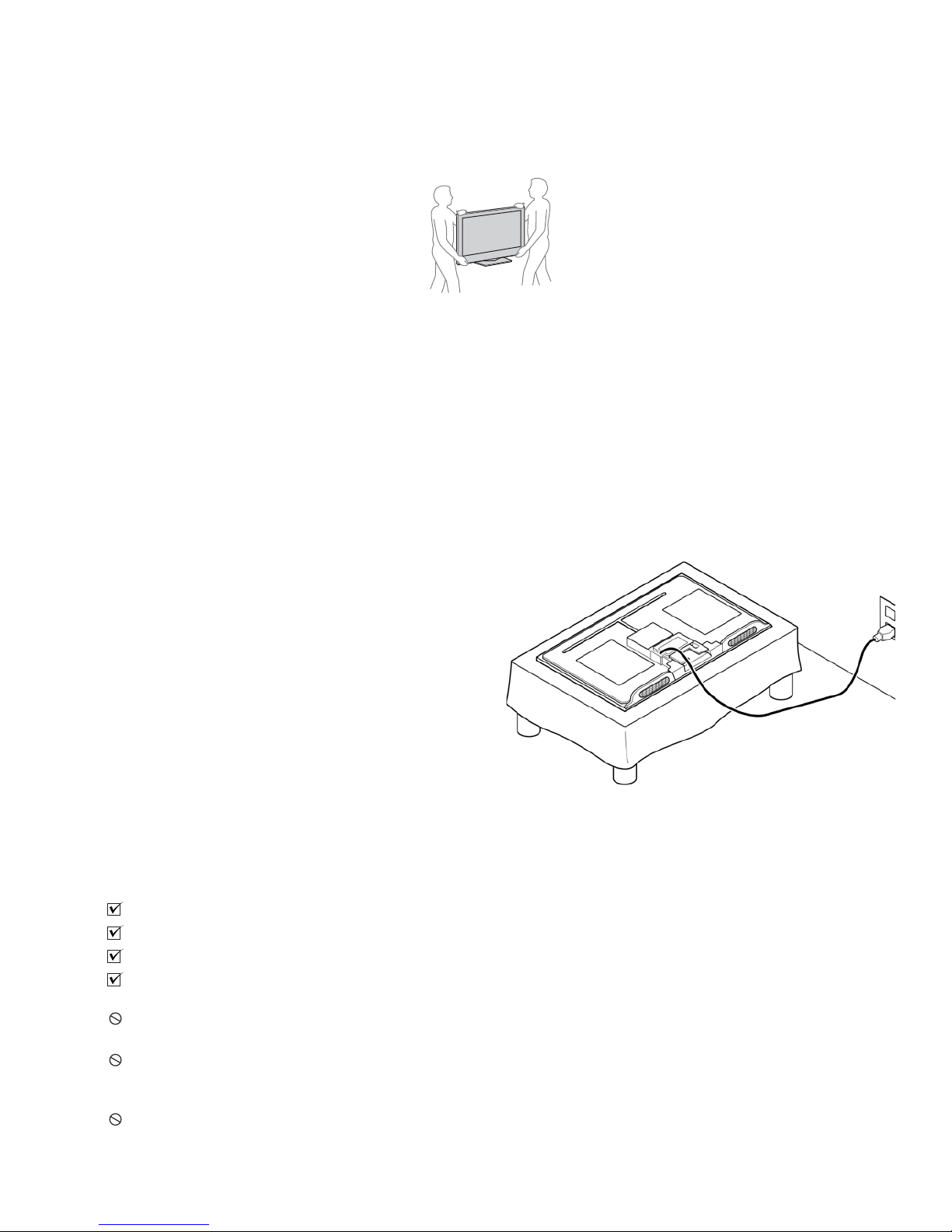
SETTING UP AND CARRYING THE TV
• Disconnect all cables when carrying the TV.
• Carry the TV with the adequate number of people; larger size TVs require two or more people.
• Correct hand placement while carrying the TV is very important for safety and to avoid damage.
Chassis: RB1FK, BL 4
SAFETY CHECK-OUT
Trouble Light
Chassis: RB1FK, BL
After correcting the original service problem, perform the
following safety checks before releasing the set to the
customer:
1. Check the area of your repair for unsoldered or
poorly soldered connections. Check the entire
board surface for solder splashes and bridges.
2. Check the interboard wiring to ensure that no
wires are “pinched” or touching high-wattage
resistors.
3. Check that all control knobs, shields, covers,
ground straps, and mounting hardware have been
replaced. Be absolutely certain that you have
replaced all the insulators.
4. Look for unauthorized replacement parts,
particularly transistors, that were installed during
a previous repair. Point them out to the customer
and recommend their replacement.
5. Look for parts which, though functioning, show
obvious signs of deterioration. Point them out to
the customer and recommend their replacement.
6. Check the line cords for cracks and abrasion.
Recommend the replacement of any such line
cord to the customer.
7. Check the antenna terminals, metal trim,
“metallized” knobs, screws, and all other exposed
metal parts for AC leakage. Check leakage as
described in “Leakage Test”.
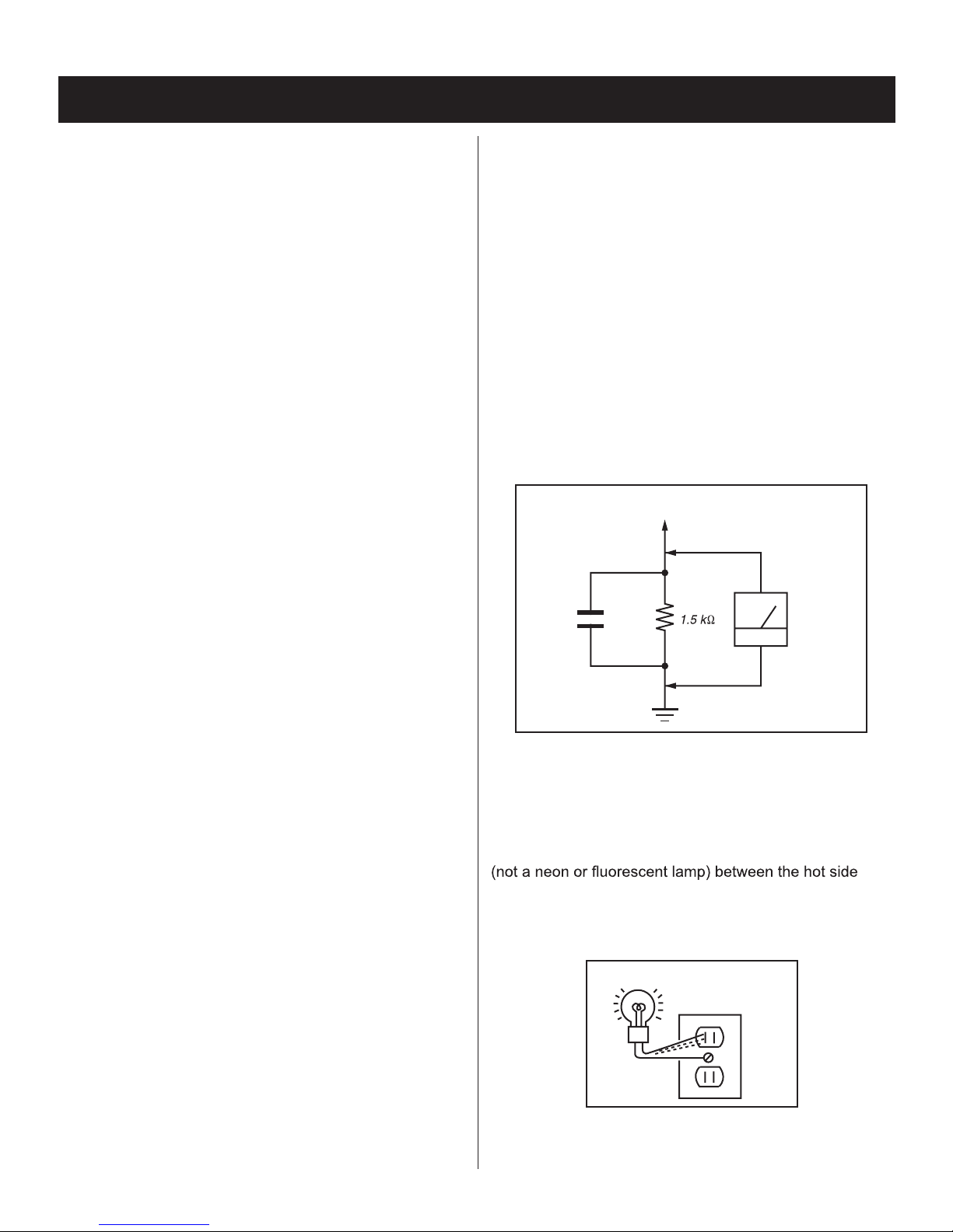
LEAKAGE TEST
The AC leakage from any exposed metal part to earth
ground and from all exposed metal parts to any exposed
metal part having a return to chassis, must not exceed
0.5 mA (500 microamperes). Leakage current can be
measured by any one of three methods.
1. A commercial leakage tester. Follow the
manufacturers’ instructions provided with the
tester.
2. A battery-operated AC milliammeter.
3. Measuring the voltage drop across a resistor
by means of a VOM or battery-operated AC
voltmeter. The “limit” indication is 0.75 V, so
analog meters must have an accurate low
voltage scale. Nearly all battery-operated digital
multimeters that have a 2 VAC range are suitable.
(see Figure A)
To Exposed Metal
Parts on Set
AC
0.15 µF
Voltmeter
(0.75V)
Chassis: RB1FK, BL 5
Earth Ground
Figure A. Use an AC voltmeter to check AC leakage.
HOW TO FIND A GOOD EARTH GROUND
The cover-plate retaining screw on most AC outlet boxes
is at earth ground. Verify the AC outlet box retaining screw
ground by connecting a 60W to 100W incandescent
of the receptacle and the retaining screw. Try both slots,
if necessary, to locate the hot side on the line; the lamp
should light at normal brilliance if the screw is at ground
potential. (see Figure B)
AC Outlet Box
Figure B. Checking for earth ground.
Chassis: RB1FK, BL
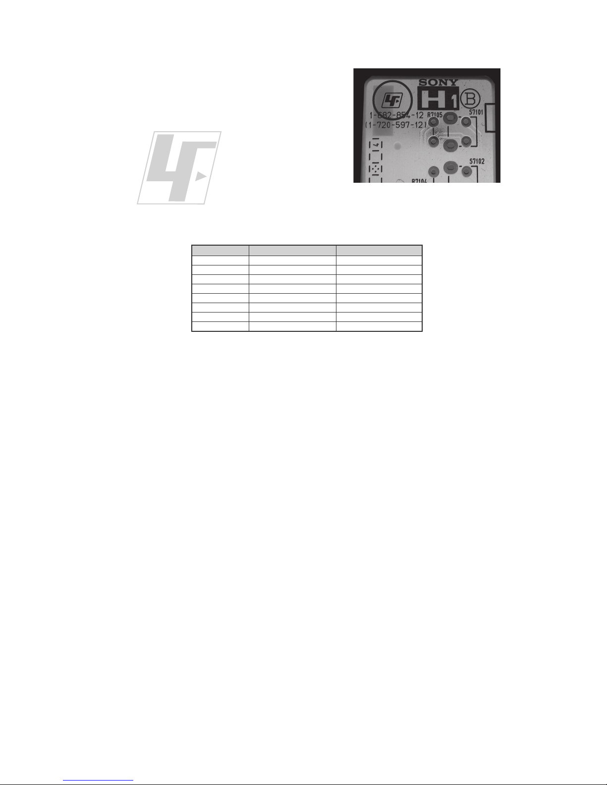
Th
e circuit boards used in these models have been processed using
Due
This
Lead Free Solder. The boards are identified by the LF logo located
close to the board designation e.g. H1 etc [ see example ]. The
servicing of these boards requires special precautions to be taken as
outlined below.
example
It is strongly recommended to use Lead Free Solder material in order to guarantee optimal quality of new solder joints.
Lead Free Solder is available under the following part numbers :
rebmuntraP retemaiD skrameR
91-500-046- m7 m3. g0 K52.0
02-500-046- m7 m4. g0 K05.0
12-500-046- m7 m5. g0 K05.0
22-500-046- m7 m6. g0 K52.0
32-500-046- m7 m8. g0 K00.1
42-500-046- m7 m0. g1 K00.1
52-500-046- m7 m2. g1 K00.1
62-500-046- m7 m6. g1 K00.1
to the higher melting point of Lead Free Solder the soldering iron tip temperature needs to be set to 370 degrees celsius.
requires soldering equipment capable of accurate temperature control coupled with a good heat recovery characteristics.
Chassis: RB1FK, BL 6
Chassis: RB1FK, BL
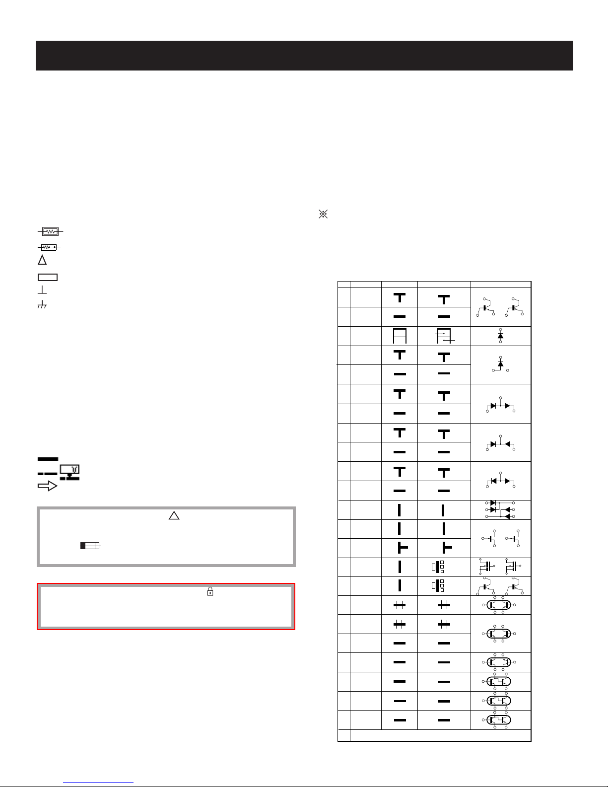
Terminal name of semiconductors in silk screen
SECTION 1: DIAGRAMS
1-1. PRINTED CIRCUIT BOARDS AND SCHEMATIC DIAGRAMS INFORMATION
REFERENCE INFORMATION
All capacitors are in µF unless otherwise noted. pF : µµF 50WV or
less are not indicated except for electrolytics and tantalums.
All electrolytics are in 50V unless otherwise specied.
All resistors are in ohms. kΩ=1000Ω, MΩ=1000kΩ
Indication of resistance, which does not have one for rating
electrical power, is as follows: Pitch : 5mm
Rating electrical power :
1
/4 W in resistance, 1/
W and 1/
10
W in chip resistance.
16
1
/4 W
: nonammable resistor
: fusible resistor
RESISTOR
: RN METAL FILM
: RC SOLID
: FPRD NONFLAMMABLE CARBON
: FUSE NONFLAMMABLE FUSIBLE
: RW NONFLAMMABLE WIREWOUND
: RS NONFLAMMABLE METAL OXIDE
: RB NONFLAMMABLE CEMENT
: ADJUSTMENT RESISTOR
COIL
: LF-8L MICRO INDUCTOR
: internal component
: panel designation and adjustment for repair
: earth ground
printed circuit ( )
Device Printed symbol Terminal name
Transistor
1
*
: earth-chassis
Transistor
2
All variable and adjustable resistors have characteristic curve B, unless
3
Diode
Cathode
otherwise noted.
Readings are taken with a color-bar signal input.
Readings are taken with a 10MΩ digital multimeter.
Voltages are DC with respect to ground unless otherwise noted.
Voltage variations may be noted due to normal production
tolerances.
All voltages are in V.
S : Measurement impossibility.
: B+line.
: B-line. (Actual measured value may be different).
: signal path. (RF)
Circled numbers are waveform references.
The components identied by shading and ! symbol are critical for safety. Replace
only with part number specied.
The symbol indicates a fast-blow fuse and is displayed on the component
side of the board. Replace only with fuse of the same rating as marked.
NOTE: The components identied by a red outline and a mark contain condential
information. Specic instructions must be adhered to whenever these components
are repaired and/or replaced.
See Appendix A: Encryption Key Components in the back of this manual.
Diode
Diode
5
Diode
6
Diode
7
8
Diode
Diode
9
Diode
10
Diode
11
Diode
12
Transistor
13
(FET)
Transistor
14
(FET)
Transistor
15
(FET)
Transistor
16
Transistor
17
Transistor
18
Transistor
19
Transistor
20
Transistor
21
Transistor
22
Transistor
23
Discrete semiconductor
–
(Chip semiconductors that are not actually used are included.)
Anode
Anode
Anode
Anode Cathode
Anode
Anode Anode
Cathode
Cathode
Anode
Anode
Cathode
4
Chassis: RB1FK, BL 7
CAPACITOR
: TA TANTALUM
: PS STYROL
: PP POLYPROPYLENE
: PT MYLAR
: MPS METALIZED POLYESTER
: MPP METALIZED POLYPROPYLENE
: ALB BIPOLAR
: ALT HIGH TEMPERATURE
: ALR HIGH RIPPLE
Collector
Base
Collector
Base
Cathode
Cathode
Common
Common
Common
Common
Common
Common
Drain
Drain
C2
C1
E1
E2
C2
B1
E2
C2
Emitter
Emitter
(NC)
(NC)
Cathode
Anode
Cathode
Cathode
Cathode
Anode
Anode
Source
Gate
Source
Gate
Source
Drain
Gate
Emitter
Collector
Base
B1 E1
B2 C1E2
B2 E2
B1 C2
B2 E2C1
B1 C2E1
B2 E2C1
B1 C2E1
B1 E1
C1(B2)
(B2)
E1
E2
C2C1
(B2)
E1
B1
C1
Anode
Circuit
D
G
D
S
B1
B1
B1
B1
B1
B1
D
G
S
S
D
G
S
C2
C1
B2
E1
E2
C2
C1
B2
E1
E2
E2
E1
B2
C1
C2
C2C1(B2)
E2
E2
E2E1(B2)
C1
C2
C2E1(B2)
C1
C2
Ver.1.6
G
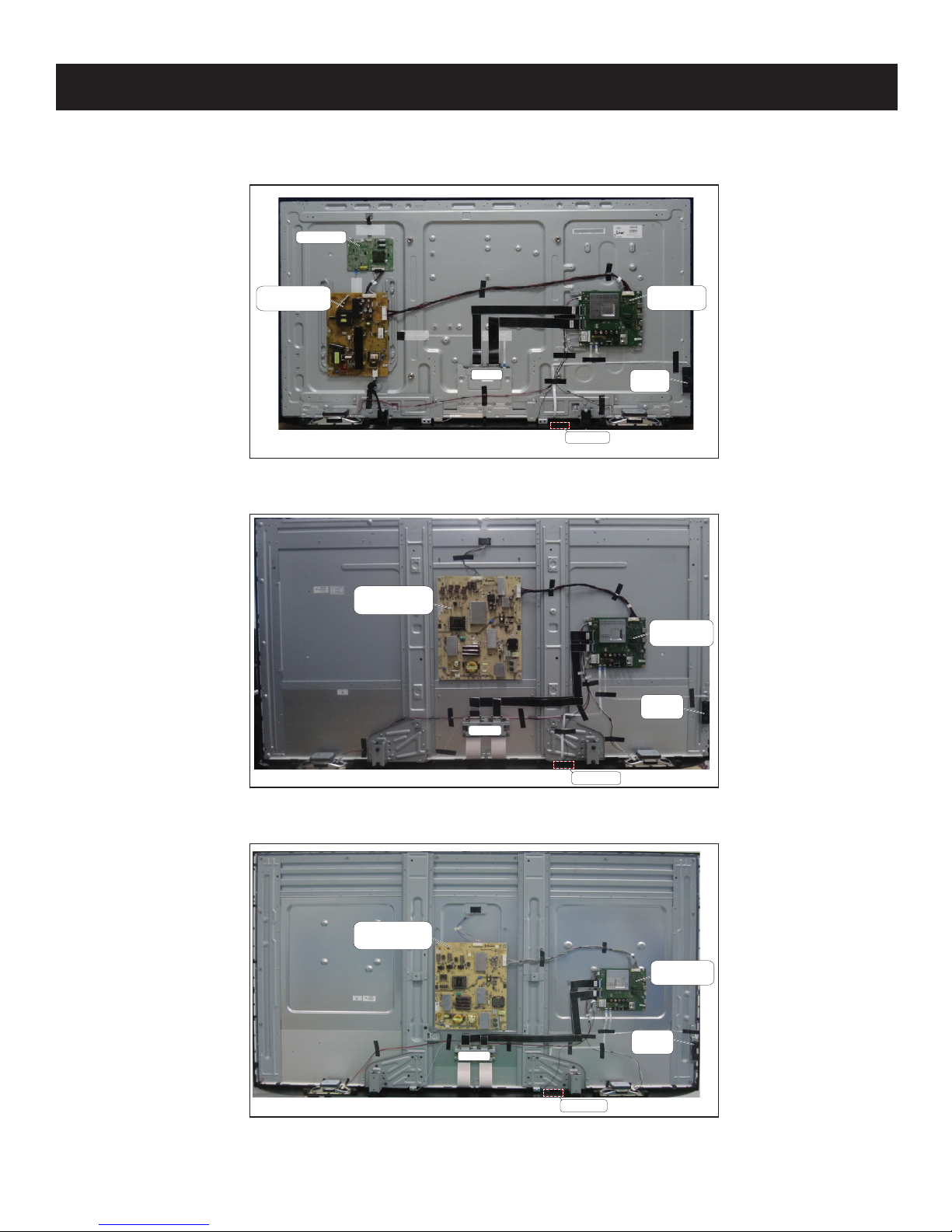
1-2. CIRCUIT BOARDS LOCATION
LD BOARD
Chassis: RB1FK, BL
SECTION 1: DIAGRAMS
POWER SUPPLY
BOARD (G4)
TCON
Figure 1-1. 50” Models
POWER SUPPLY
BOARD (GE60)
TCON
H BOARD
4
MAIN BOARD
(A BOARD)
SWITCH
UNIT
MAIN BOARD
(A BOARD)
SWITCH
UNIT
Chassis: RB1FK, BL 9
Figure 1-2. 60” Models
POWER SUPPLY
BOARD (GE70)
TCON
Figure 1-3. 70” Models
H BOARD
H BOARD
MAIN BOARD
(A BOARD)
SWITCH
UNIT
Chassis: RB1FK, BL 9
Chassis: RB1FK, BL
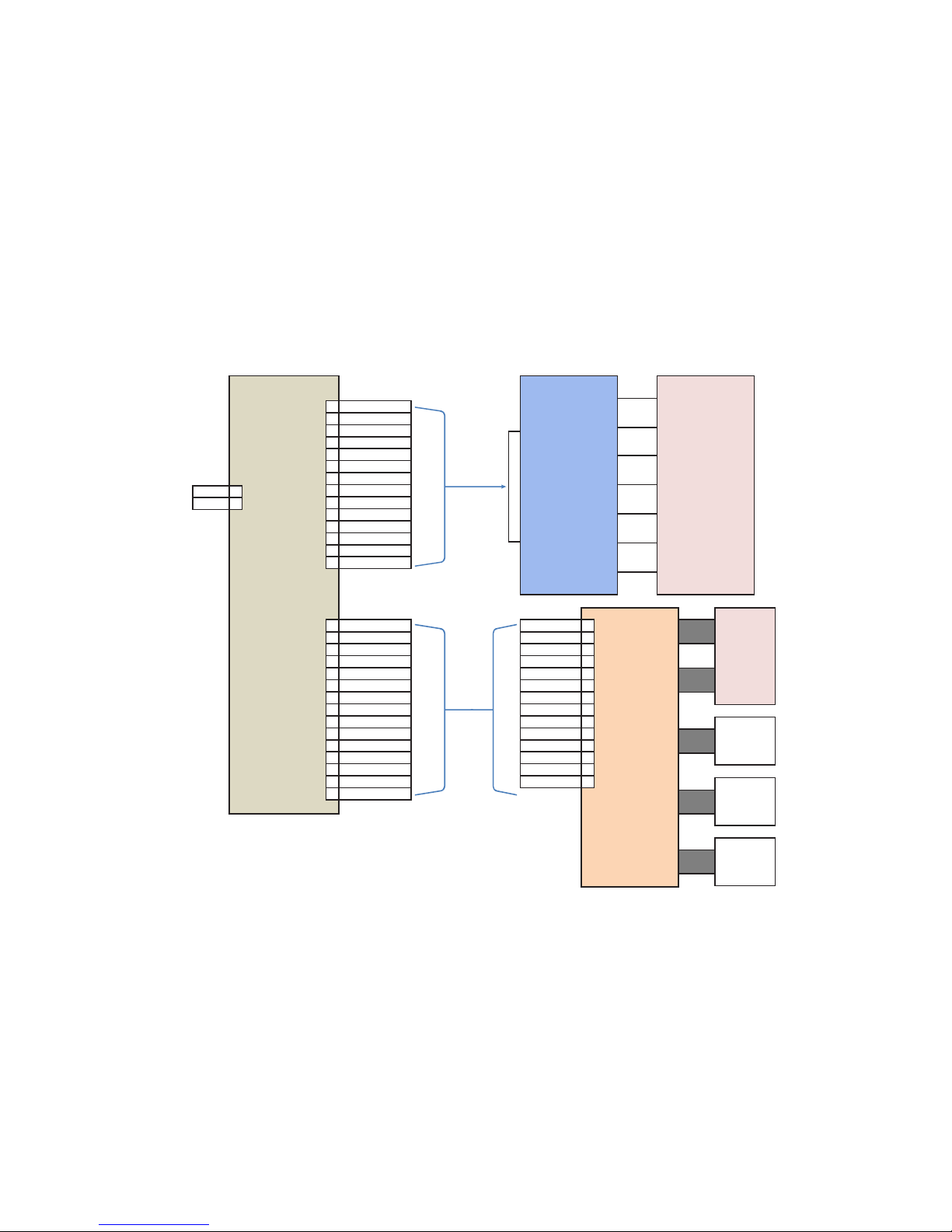
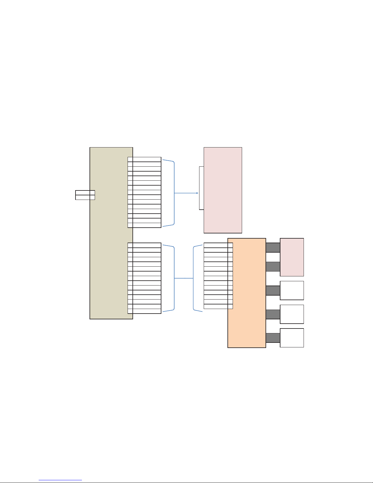
1-3. CONNECTOR DIAGRAMS
FOR 50” MODELS ONLY
Power Supply
G4(50”)
CN6401 CN201
CN6402
CN6101
3_3VSB
ACD
Power ON
Audio_12V_GND
Audio_12VGND
REG_12V_GND
REG_12V_GND
Audio_12V
REG_12V
REG_12V
REG_12V
BL_Error
BL_ON
PWM_DIMMER
NC
UNAEG_24V
UNAEG_24V
UNAEG_24V
UNAEG_24V
UNAEG_24V
GND
GND
GND
GND
GND
BL_ERR
BL_ON
PWM_DIMMER
NC
AC_N
ACL_L
1
2
3
4
5
6
7
8
9
#
#
#
#
#
1
2
1
2
3
4
5
6
7
8
9
#
#
#
#
#
#
1
5
6
9
#
2
7
#
3
8
#
#
#
4
SB_3.3V
AC_DET#
PSU_EN#
GND
GND
GND
GND
AUD_12V
PSU_12V
PSU_12V
TCON_12V
PSU_BL_ERR#
PSU_BL_EN#
PSU_BL_PWM
Converter Backlight LED
Main
Board
Panel
T-CON
CN4005
CN4004
CN4007
CN4007
CN8001
L/R
FFC
10pin
FFC
6pin
FFC
51pin
FFC
41pin
Keypad
IR/LED
/ABS
Speaker
Chassis: RB1FK, BL 10
Chassis: RB1FK, BL
1-3. CONNECTOR DIAGRAMS
Power Supply
DPS-248BP(70”)
CN2 CN201
CN3
CN1
3_3VSB
ACD
Power ON
Audio_12V_GND
Audio_12VGND
REG_12V_GND
REG_12V_GND
Audio_12V
REG_12V
REG_12V
REG_12V
BL_Error
BL_ON
PWM_DIMMER
NC
LED1+
LED1-
LED2+
LED2-
LED3+
LED3-
LED4+
LED4-
AC_N
ACL_L
1
2
3
4
5
6
7
8
9
10
11
12
13
14
15
1
2
1
2
3
4
5
6
7
8
9
10
11
12
13
14
15
1
5
6
9
11
2
7
12
3
8
10
13
14
4
SB_3.3V
AC_DET#
PSU_EN#
GND
GND
GND
GND
AUD_12V
PSU_12V
PSU_12V
TCON_12V
PSU_BL_ERR#
PSU_BL_EN#
PSU_BL_PWM
DPS-200PP(60”)
Backlight LED
Main
Board
Panel
T-CON
CN4005
CN4004
CN4007
CN4007
CN8001
L/R
FFC
10pin
FFC
6pin
FFC
51pin
FFC
41pin
Keypad
IR/LED
/ABS
Speaker
FOR 60” & 70” MODELS ONLY
Chassis RB1FK, BL 11
Chassis RB1FK, BL
A
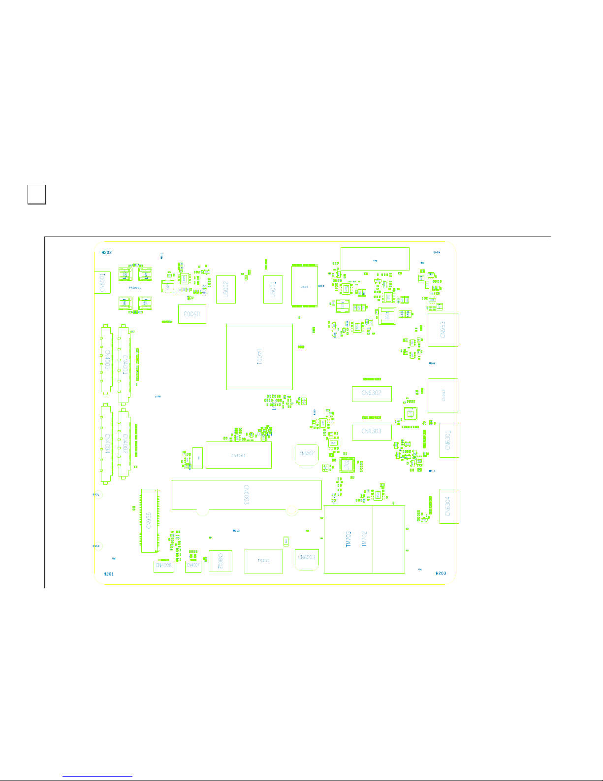
1 | 2 | 3 | 4 | 5 | 6 | 7 | 8 | 9 | 10 | 11 | 12 | 13 | 14 | 15 | 16 | 17 | 18 | 19 | 20 | 21 | 22 | 23 | 24 | 25 | 26 |
A
—
B
—
C
—
D
—
E
—
F
—
[SYSTEM POWER/YPBPR/AV/SPDIF/USB/HDMI/DDR/FLASH/PREAMP/AUDIO AMP/LVDS/DEMOD/TUNER/ETHERNET]
A BOARD COMPONENT SIDE
1-4. MAIN BOARD (A BOARD)
Chassis RB1FK, BL 12
Chassis RB1FK, BL
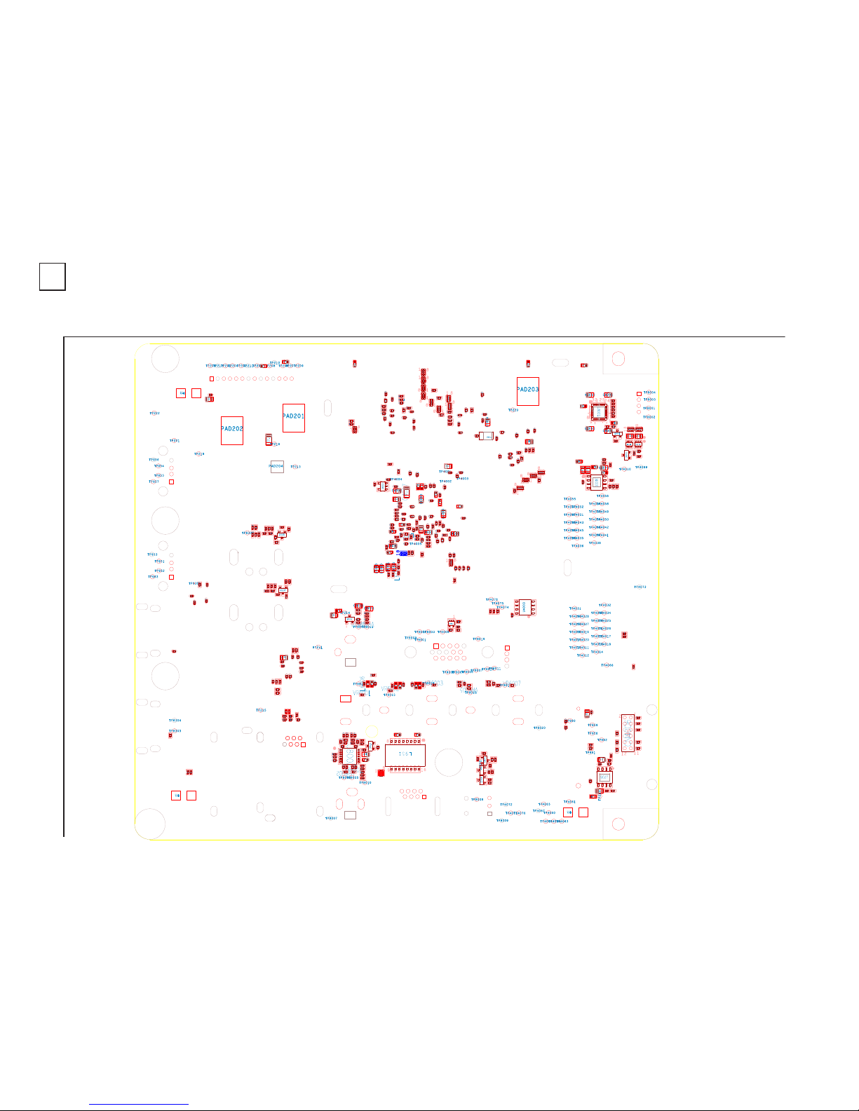
1 | 2 | 3 | 4 | 5 | 6 | 7 | 8 | 9 | 10 | 11 | 12 | 13 | 14 | 15 | 16 | 17 | 18 | 19 | 20 | 21 | 22 | 23 | 24 | 25 | 26 |
A
—
B
—
C
—
D
—
E
—
F
—
A
[SYSTEM POWER/YPBPR/AV/SPDIF/USB/HDMI/DDR/FLASH/PREAMP/AUDIO AMP/LVDS/DEMOD/TUNER/ETHERNET]
A BOARD CONDUCTOR SIDE
Chassis RB1FK, BL 13
Chassis RB1FK, BL
A BOARD SCHEMATIC
A BOARD SCHEMATIC DIAGRAM (1 OF 26)
1
1
2
2
3
3
4
4
5
5
6
6
7
7
8
8
A A
B B
C C
D D
E E
F F
G G
H H
Drawn :
Checked
Approved
File Name :
PART NO.
Date :
LY.REV :
REV.
SHEET
____ OF ____
PWB :
DESCRIPTION :
1
<RevCode>
10-20-2005
297005040100.BRD
00
297005040100.DSN
10-20-2005
10-20-2005
2970050401-SC
25
SCHEMATIC OF LCD TV MONITOR
Monday, January 07, 2013
Drawn :
Checked
Approved
File Name :
PART NO.
Date :
LY.REV :
REV.
SHEET
____ OF ____
PWB :
DESCRIPTION :
1
<RevCode>
10-20-2005
297005040100.BRD
00
297005040100.DSN
10-20-2005
10-20-2005
2970050401-SC
25
SCHEMATIC OF LCD TV MONITOR
Monday, January 07, 2013
Drawn :
Checked
Approved
File Name :
PART NO.
Date :
LY.REV :
REV.
SHEET
____ OF ____
PWB :
DESCRIPTION :
1
<RevCode>
10-20-2005
297005040100.BRD
00
297005040100.DSN
10-20-2005
10-20-2005
2970050401-SC
25
SCHEMATIC OF LCD TV MONITOR
Monday, January 07, 2013
8001~8299
REFERENCE REFERENCEPAGE. FUNCTION PAGE. FUNCTION
01. Page List
02. BLOCK DIAGRAM.
04. Power Distribution I.
05. Power Distribution II.
07. Power Distribution IV.
09. YPBPR & AV Interface.
11. HDMI Interface II
10. HDMI Interface I
12. RF Silicon Tuner
13. RF Demodulator
06. Power Distribution III.
15. MT5396 DDR I
16. MT5396 DDR II
17. MT5396 FRONT END
5001~5199 (For DDR)
201~299
2201~2299
6001~6099
4001~4399
08. VGA Interface.
6301~6399
22. AUDIO AMPLIFIER.
23. AUDIO LINE-OUT & SPDIF.
26. History.
24. Panel LVDS Interface.
03. Power Structure.
18. MT5396 Ethernet & USB.
951~999 (Ethernet
& USB & WIFI)
4001~4399
14. MT5396 Power
701~799
19. MT5396 Flash & Reset.
20. MT5396 RX/TX
21. MT5396 CI & Sub-BD
25. Ralink WiFi Module.
951~999 (Ethernet
& USB & WIFI)
Chassis RB1FK, BL 14
Chassis RB1FK, BL
A BOARD SCHEMATIC DIAGRAM (2 OF 26)
1
1
2
2
3
3
4
4
5
5
6
6
7
7
8
8
A
A
B
B
C
C
D
D
E
E
F
F
G
G
H
H
Drawn :
Checked
Approved
File Name :
PART NO.
Date :
LY.REV :
REV.
SHEET
____ OF ____
PWB :
DESCRIPTION :
2
<RevCode>
10-20-2005
297005040100.BRD
00
297005040100.DSN
10-20-2005
10-20-2005
2970050401-SC
25
SCHEMATIC OF LCD TV MONITOR
Monday, January 07, 2013
Drawn :
Checked
Approved
File Name :
PART NO.
Date :
LY.REV :
REV.
SHEET
____ OF ____
PWB :
DESCRIPTION :
2
<RevCode>
10-20-2005
297005040100.BRD
00
297005040100.DSN
10-20-2005
10-20-2005
2970050401-SC
25
SCHEMATIC OF LCD TV MONITOR
Monday, January 07, 2013
Drawn :
Checked
Approved
File Name :
PART NO.
Date :
LY.REV :
REV.
SHEET
____ OF ____
PWB :
DESCRIPTION :
2
<RevCode>
10-20-2005
297005040100.BRD
00
297005040100.DSN
10-20-2005
10-20-2005
2970050401-SC
25
SCHEMATIC OF LCD TV MONITOR
Monday, January 07, 2013
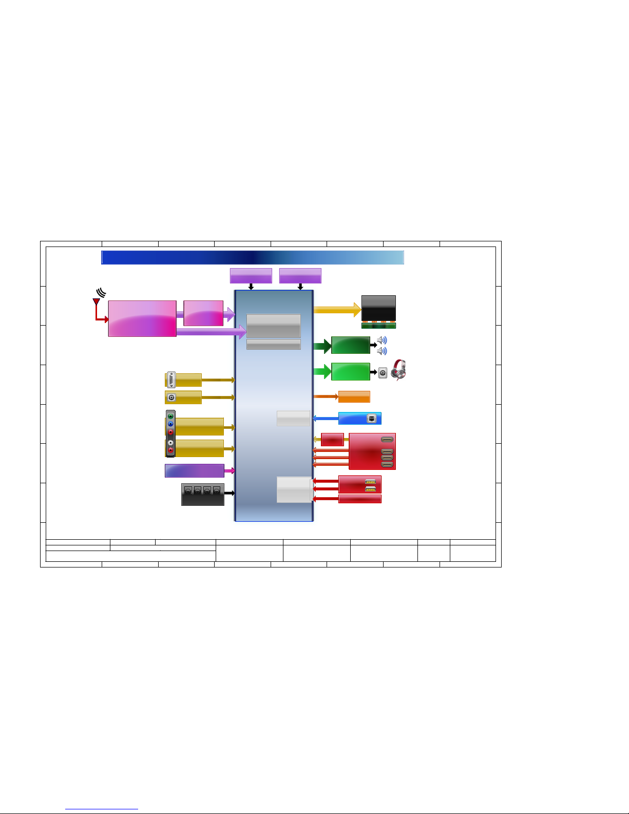
MT5396
SPDIF
Line out Driver
APA2172
Amplifier
YDA176
Speaker
(8 Ω/10W)
R
L
Line out / HP
LVDS
I2S
PWM
IF
TS
IF
LCM Panel
(120/100Hz)
Ethernet PHY
Tuner
NA/MX: RA227TN
PAA/PAD/(CHA/CHD): RE227TN
CHA/CHD: RC221TN
COL/CHI/PE: RB221TN
Demod.
CHD: CXD2840ER
CHI/PE: CXD2838ER
COL: CXD2837ER
Demod.
ATSC/DVB-T/DVB-C
120 Hz MEMC
DDR3
2Gx2+1Gx1
NAND Flash
256 MB
HDMI1 (ARC)
MHL IC
SII1292
HDMI2 (MHL)
HDMI 3
HDMI 4
USB 2
WiFi
Ethernet
USB 1
Keypad
IR / LED / Light Sensor
YPbPr/CVBS
VGA-R/L
VGA
YPbPr-R/L/CVBS-R/L
Block Diagram (BL)
Chassis RB1FK, BL 15
Chassis RB1FK, BL
A BOARD SCHEMATIC DIAGRAM (3 OF 26)
1
1
2
2
3
3
4
4
5
5
6
6
7
7
8
8
A A
B B
C C
D D
E E
F F
G G
H H
Drawn :
Checked
Approved
File Name :
PART NO.
Date :
LY.REV :
REV.
SHEET
____ OF ____
PWB :
DESCRIPTION :
3
<RevCode>
10-20-2005
297005040100.BRD
00
297005040100.DSN
10-20-2005
10-20-2005
2970050401-SC
25
SCHEMATIC OF LCD TV MONITOR
Monday, January 07, 2013
Drawn :
Checked
Approved
File Name :
PART NO.
Date :
LY.REV :
REV.
SHEET
____ OF ____
PWB :
DESCRIPTION :
3
<RevCode>
10-20-2005
297005040100.BRD
00
297005040100.DSN
10-20-2005
10-20-2005
2970050401-SC
25
SCHEMATIC OF LCD TV MONITOR
Monday, January 07, 2013
Drawn :
Checked
Approved
File Name :
PART NO.
Date :
LY.REV :
REV.
SHEET
____ OF ____
PWB :
DESCRIPTION :
3
<RevCode>
10-20-2005
297005040100.BRD
00
297005040100.DSN
10-20-2005
10-20-2005
2970050401-SC
25
SCHEMATIC OF LCD TV MONITOR
Monday, January 07, 2013
 Loading...