

Page 1
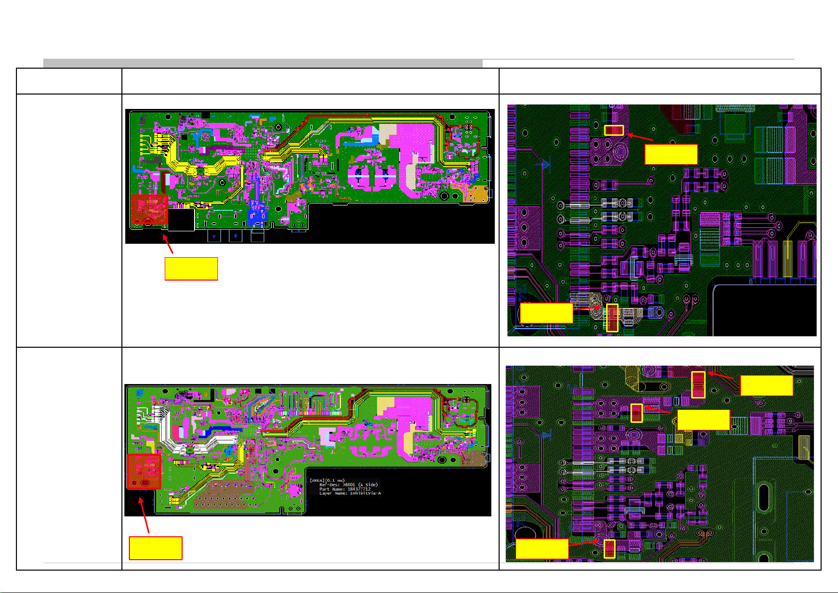
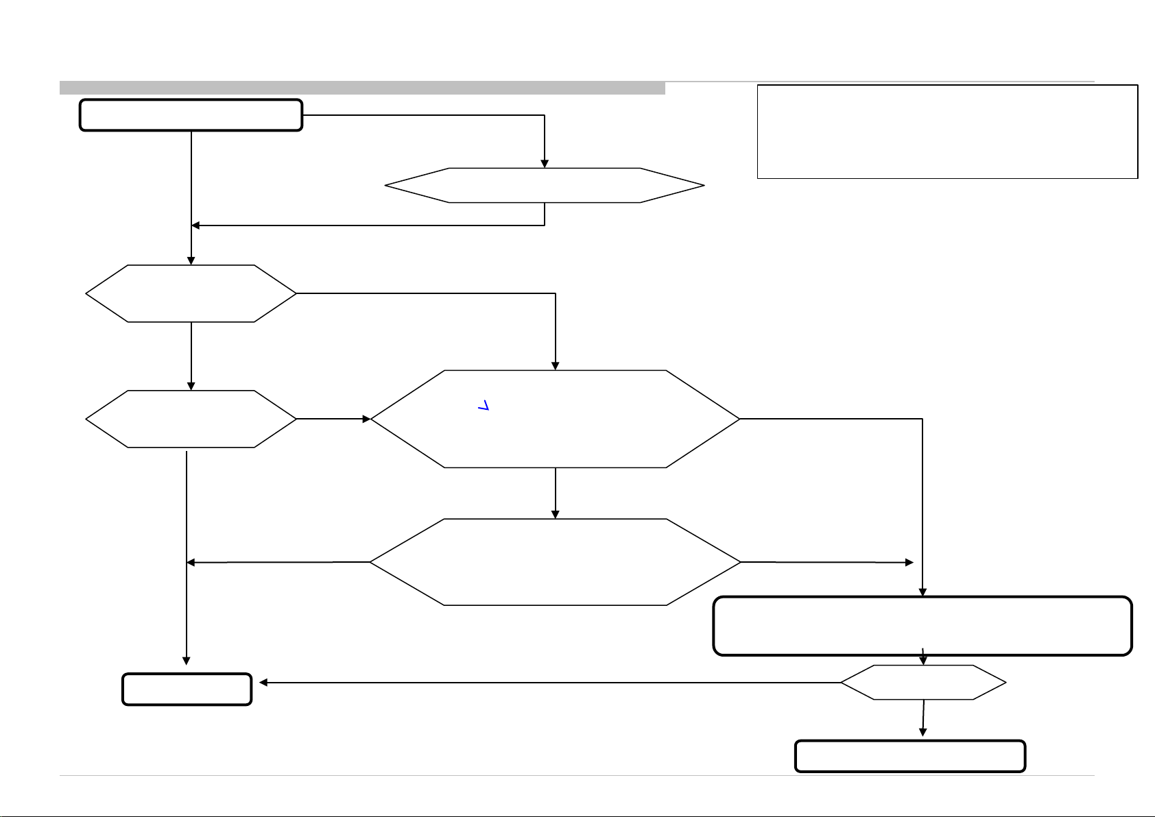
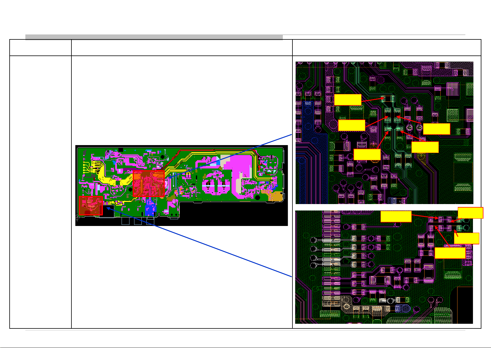
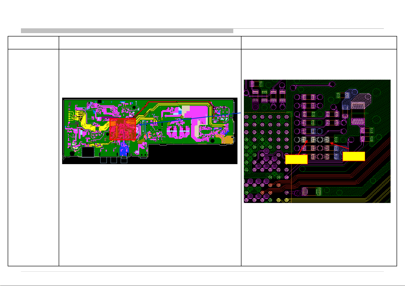
HISTORY INFORMATION FOR THE FOLLOWING MANUAL:
SERVICE MANUAL (COMMON)
Version Date Subject
1 01/2016 1st Issue.
GN2S CHASSIS
Segment: QW
LCD TV
9-888-190-01
For SM - Unique , please refer :
9-888-190-Ax ( America )
9-888-190-Cx ( China)
9-888-190-Ex ( Europe )
9-888-190-Px ( Pan Asia)
Page 2
SERVICE MANUAL (COMMON)
GN2S CHASSIS
Segment: QW
LCD TV
Page 3
MODEL LIST
THIS SERVICE MANUAL CONTAINS COMMON INFORMATION FOR BELOW REGIONS AND MODELS:
REGION
ASIA AMERICA EUROPE
CHINA
MODEL
KLV-32W6*D KLV-40W6*D KLV-48W6*D
KDL-32W6*D KDL-40W6*D KDL-48W6*D KDL-55W6*D
Page 4
Section Title
1. SAFETY NOTES
1
1
1
1
1
1
1
1
)…………………………………….
2. SELF DIAGNOSTIC FUNCTION
2
Overview of Control Buttons .................................................................. .
2
……….....................................................................
2
………………........................................................................
2
2
............................................................................................
3. TROUBLE SHOOTING
3
.............................................................................................
3
3
No Picture................................................................ ............ ............ ........ .
3
TABLE OF CONTENTS
Section Title
4. SERVICE ADJUSTMENTS
4
Accessing Service Mode .....................................................................
4
Accessing Software Version....................……….………………………
4
Accessing Self Diagnostic History………………………………..……..
4
Accessing Self Diagnostic Menu………………………………………...
4
Accessing Serial Number Edit……………….…………………………..
4
Accessing Model Number Setting........................................................
4
White Balance..................................................... ............... ............ ......
4
Aging Mode...................................................... .................. ................ ..
4
Tuner Detection........................................................ ............... .............
5. DIAGRAMS
5
Circuit Board Location .........................................................................
5
Block Diagram......................................................................................
5
Connector Diagram
Page
-1. Warnings and Caution………………………………………………………. 5
-2. Caution Handling of LCD Panel ......…………….................................... 5
-3. Caution About the Lithium Battery……………......................................... 6
-4. Safety Check Out ........................……………......................................... 6
-5. Leakage Test .......................................................................................... 6
-6. How to Find a Good Earth Ground………………………………………… 6
-7. Lead Free Information….…………………………………………………… 7
-8. Handling the Flexible Flat Cable (FFC
-1.
-2. LED Display Control
-3. LED Pattern
-4. Standby LED Error Display…………………………………………………. 8
-5. Triage Chart
-1. LED Blinking
-2. No Power…….……………………………………………………………….. 28
-3.
-4. No Sound.............................………………………………………….......... 107
7
8
8
8
9
12
54
Page
-1.
-2.
-3.
-4.
-5.
-6.
-7.
-8.
-9.
-1.
-2.
-3.
Please refer to Service Procedure for Panel , Board and Software Change / Upgrade
Manual , part number 9-888-196-0x in TISS .
Please refer Service Manual – Unique for below information :
………………………………………...................... 147
129
129
130
130
132
133
135
139
140
143
144
-Safety Warnings
-Wire Dressing
-Circuit Board Location
-Disassembly and Exploded View.
Note: Pictures provided in this Ser vice Manual might have slight difference from the
actual sets.
4
Page 5
SECTION 1
4
3) Do not leave the module in high temperature or in areas of high humidity for
6) Di
klight (CCFL)
Correct
hand
placement
while
carrying
theTVis
very
important
for
8) Use care when handling the wires or connectors of the inverter circuit.
components
with
Sony
parts
whose
part
numbers
appear
as
shown
in
this
p
th
hile the TV is f
p
p
SAFETY NOTES
1-1. Warnings and Caution
1) These servicing instructions are for use by qualified service personnel only.
2) To reduce the risk of electric shock, do not perform any servicing other than
that contained in the operating instructions unless you are qualified to do so.
3) An isolation transformer should be used during any service to avoid
Possible shock hazard, because of live chassis. The chassis of this receiver is
directly connected to the ac power line.
4)Be sure tofollow these guidelines to protect yourproperty and
avoid causing serious injury :
• Carry the TV with an adequate number of people; larger size TVs require
two or more people.
•
safety and to avoid damages.
5) Components identified by shading and mark on the exploded views,
and in the parts list are critical for safe operation. Replace these
manual or in supplements published by Sony. Circuit adjustments that are
critical for safe operation are identified in this manual. Follow these
procedures whenever critical components are replaced or improper
eration is suspected.
o
!
1-2. Caution Handling of LCD Panel
When repairing the LCD Panel, make sure you are grounded with a wrist band.
When repairing the LCD Panel on the wall, the panel must be secured using the
mounting holes on the rear cover.
1) Do not press the panel or frame edge to avoid the risk of electric shock.
2) Do not scratch or press on the panel with any sharp objects.
an extended period of time.
4) Do not expose the LCD panel to direct sunlight.
5) Avoid contact with water. It may cause short circuit within the module.
sconnect the AC power when replacing the bac
inverter circuit. (High voltage occurs at the inverter circuit at 650Vrms)
7) Always clean the LCD panel with a soft cloth material.
Damaging the wires may cause a short circuit.
9) Protect the panel from ESD to avoid damaging the electronic circuit (C-MOS).
10) During the repair, DO NOT leave the Power On or Burn-in period for more
an 1 hour w
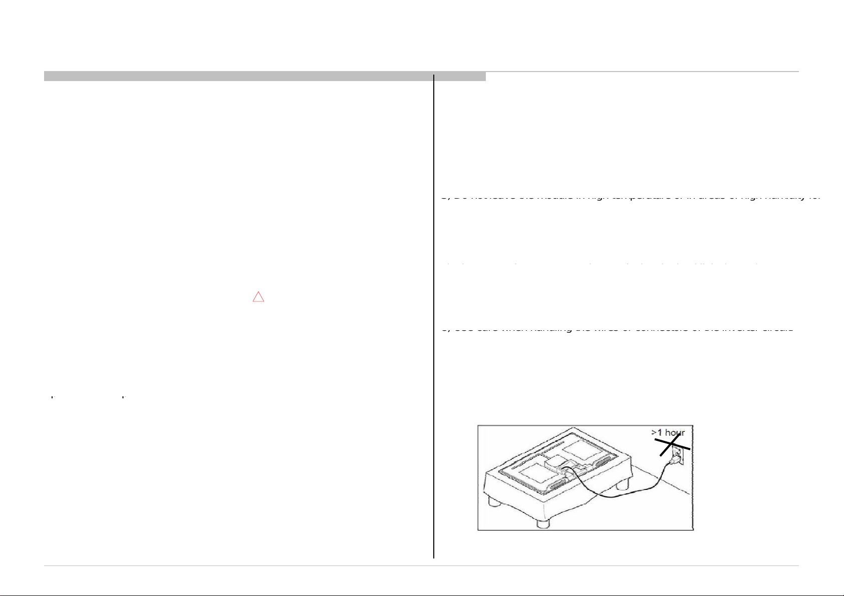
ace down on a cloth.
or
Figure 1. TV is faced down on a cloth during repair.
5
Page 6
1-3. Caution About the Lithium Battery
1) Danger of explosion if battery is incorrectly replaced. Replace only with
the same or equivalent type.
2) Outer case broken battery should not contact to water.
1-4. Safety Check-Out
After correcting the original service problem, perform the following
safety checks before releasing the set to the customer:-
1) Check the area of your repair for unsoldered or poorly soldered
connections. Check the entire board surface for solder splashes and bridges.
2) Check the inter board wiring to ensure that no wires are pinched or
contact high-wattage resistors.
3)Check all control knobs, shields, covers, ground straps and mounting
hardware have been replaced. Be absolutely certain you have replaced all
the insulators.
4) Look for unauthorized replacement parts, particularly transistors that
were installed during a previous repair. Point them out to the customer and
recommend their replacement.
5) Look for parts which, though functioning show obvious signs of
deterioration. Point them out to the customer and recommend their
replacement.
6) Check the line cords for cracks and abrasion. Recommend the
replacement of any such line cord to the customer.
7) Check the antenna terminals, metal trim, metalized knobs, screws and all
other exposed metal parts for AC leakage. Check leakage test as described
next.
8. For safety reasons, repairing the Power board and/or Inverter board is
prohibited.
1-5.Leakage Test
The AC leakage from any exposed metal part to earth ground and from all
exposed metal parts to any exposed metal part having a return to chassis must
not exceed 0.5mA (500 microamperes).
Leakage current can be measured by any one of the three methods:-
1) A commercial leakage tester such as the SIMPSON 229 or RCA WT540A.
Follow the manufacturers instructions to use those instructions.
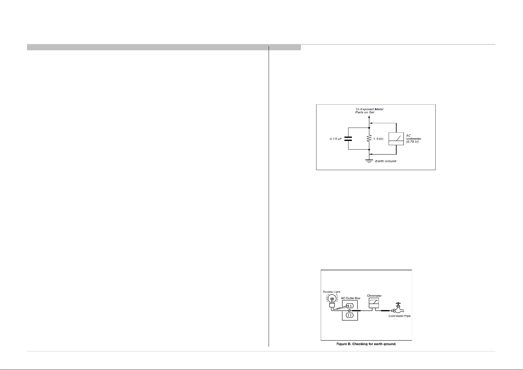
2) A battery-operated AC milliampmeter The DATA PRECISION 245 digital
multimeter is suitable for this job.
3) Measuring the voltage drop across a resistor by means of a VOM or battery
operated AC voltmeter. The 'limit' indication is 0.75V so analog meters must
have an accurate low voltage scale. The SIMPSON'S 250 and SANWA SH63TRD are examples of passive VOMs that are suitable. Nearly all battery
operated digital multimeter that have a 2 VAC range are suitable.
(see Figure 2.)
Figure 2. AC voltmeter to check AC leakage
1-6. How to Find a Good Earth Ground
1) A cold-water pipe is a guaranteed earth ground; the cover-plate retaining
screw on most AC outlet boxes is also at earth ground.
2) If the retaining screw is to be used as your earth ground, verify that it is at
ground by measuring the resistance between it and a cold-water pipe with an
ohmmeter. The reading should be zero ohms.
3) If a cold-water pipe is not accessible, connect a 60- to 100-watt troublelight (not a neon lamp) between the hot side of the receptacle and the
retaining screw. Try both slots, if necessary, to locate the hot side on the line;
the lamp should light at normal brilliance if the screw is at ground potential
(see Figure 3).
Figure 3. Checking for earth
ground.
6
Page 7
1-7. Lead Free Information
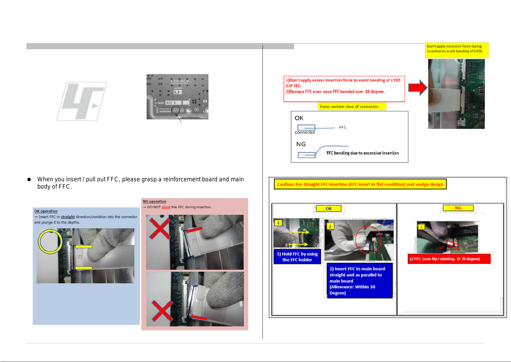
The circuit boards used in these models have been processed using Lead
Free Solder. The boards are identified by the LF logo located close to the
board designation.
The servicing of these boards requires special precautions. It is strongly
Figure 4: LF Logo
Figure 5: LF logo on circuit board
recommended to use Lead Free Solder material in order to guarantee optimal
quality of new solder joints.
1-8. Handling the FLEXIBLE FLAT CABLE (FFC)
When you insert / pull out FFC, please grasp a reinforcement board and main
body of FFC.
7
Page 8
1-8. Handling the FLEXIBLE FLAT CABLE (FFC)
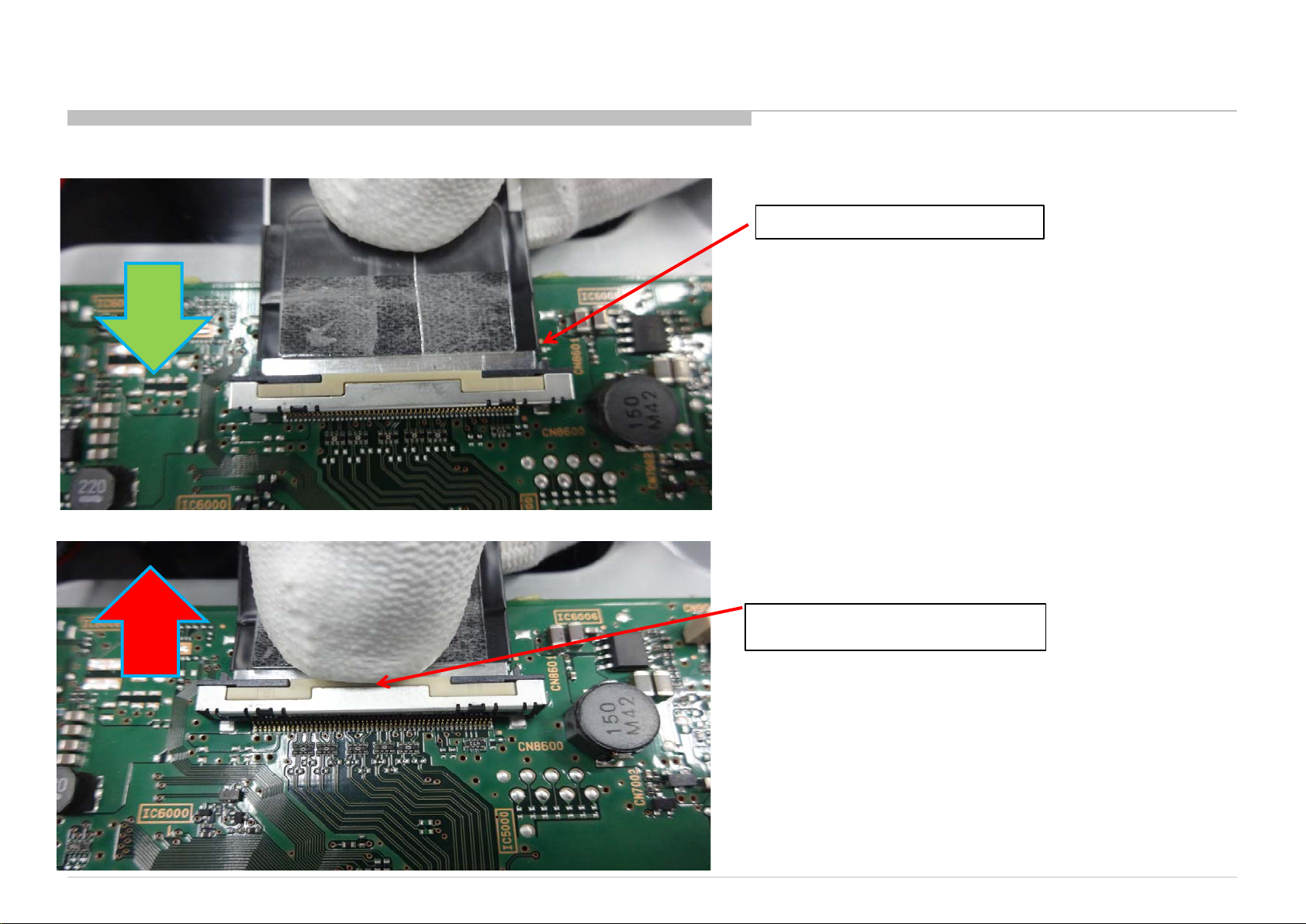
<INSERTION>
Insert properly without slanting
<PULL OUT>
Press release button at the same
time pull out FFC cable
8
Page 9
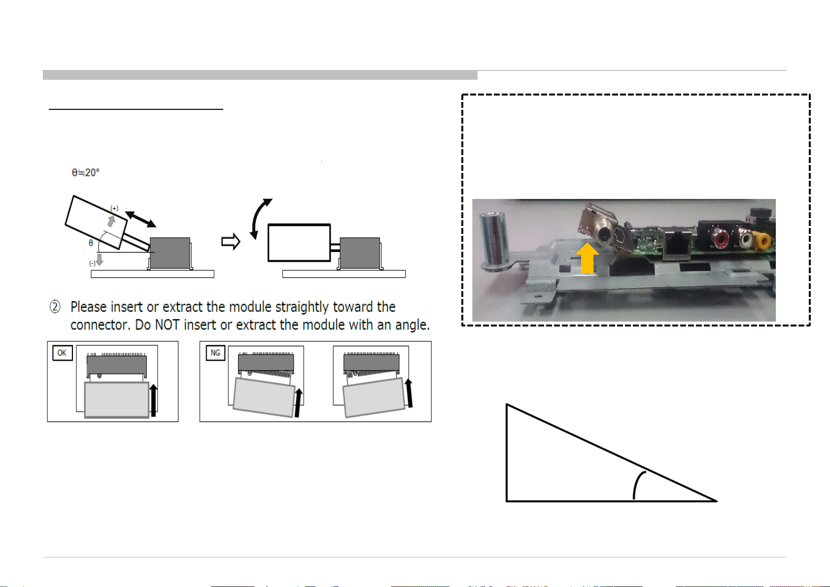
1-9. Assemble and Dissemble Tuner Module
Tuner Module treatmen t way
1. The insertion & extraction angle of the module is permitted to
specified degree for connector
Push down to screw.
For removing Tuner Module,
After un screwed, Automatically the Module
will float to correct degree.
So please extract it with keeping this degree.
20°
Reference paper for 20 degree
(If need please use for fit by cutting this paper)
20°
9
Page 10
SECTION 2
SELF DIAGNOSTIC FUNCTION
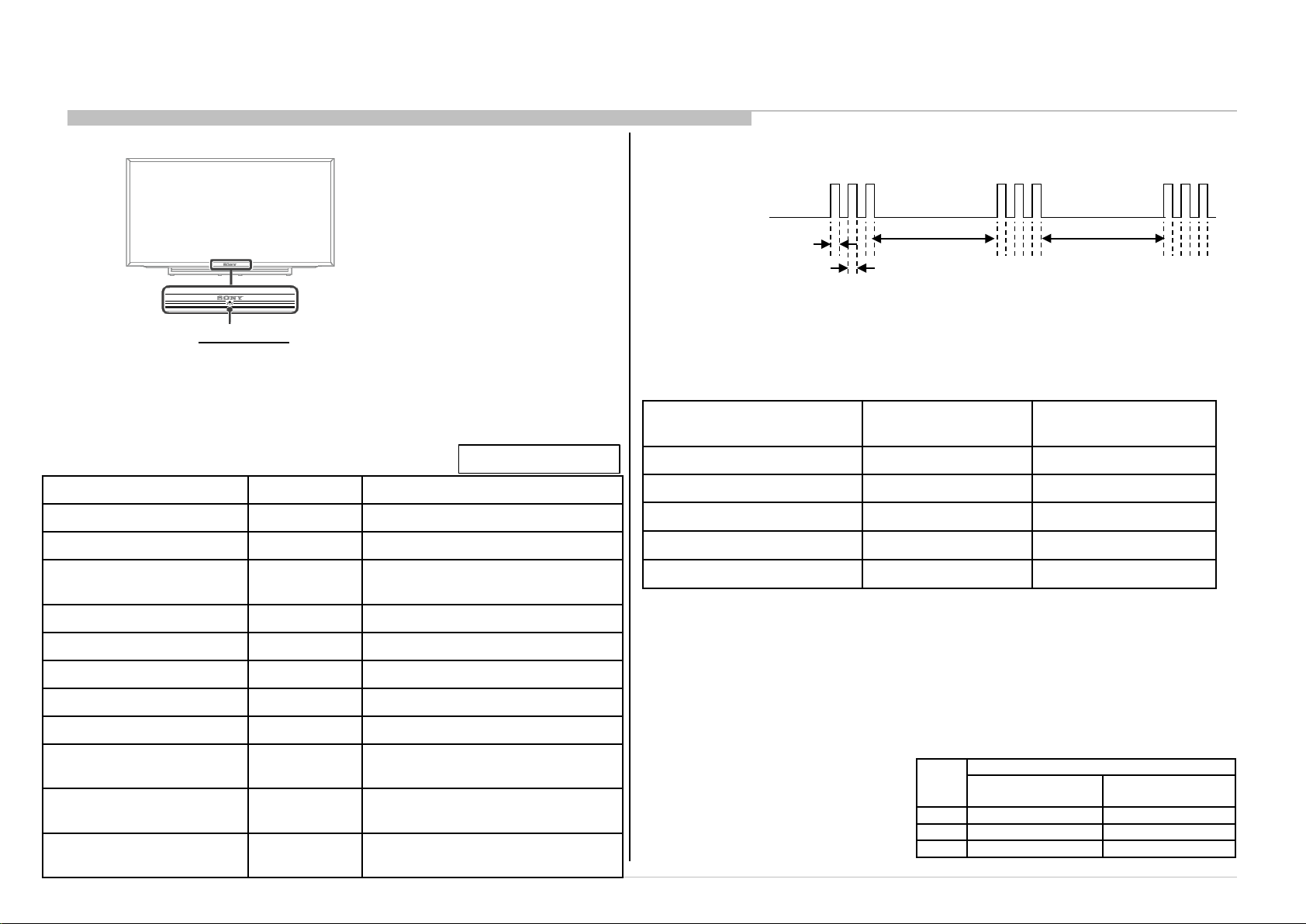
2-1. Overview of Control Buttons
LED Indicator
• Lights up in green when you select “Picture Off”.
• Lights up in amber when you set the timer or
“Photo Frame Mode”.
• Lights up in green when the TV is turned on.
• Flashes while the remote is being operated.
2-2. LED Display Control
Status LED Colour Remarks
Power Off ( AC Off and *1) OFF *1 power switch off (by touch button)
Power On Green
Standby(by remote control off
and Side Key off)
OFF
Amber = Red + Green
2-3. LED Pattern
When safety shutdown occurs, Standby LED displ ay reports the cause by using the lightning
0.5sec
.
3.0sec 3.0sec
patterns as indicated below
0.5sec
Example: The figure above shows LED display when SHUTDOWN is caused by Audio
Error. It repeats flashing for a specifi ed num ber of tim es i n 0.5sec/c ycle and has a 3 seconds interval of li ghting
off. Please note that a 3 seconds interval of lighting off is fixed regardless of abnormal state types.
2-4. Standby LED Error Display
The Number of Standby LED
(RED blinking)
2 Main Power Error AC adapter Error
3 Audio Error B* board Error
4 Panel Power Error B* board Error
5 Panel I2C COMM Error B* or Source board Error
6 Backlight Error B* board Error
Error Detection Error Location
Picture Off Green
Set "Sleep Timer" Amber
Set "On Timer” ( Power On ) Amber
Set "On Timer”( Standby ) Amber
Picture Frame Amber
Failure Red Blinking
Error of panel ID
Software Updating
6
Amber/Green
Blinking
Amber
Blinking
The number of LED blinking indicates
cause of failure.
Blinking:0.5sec Amber/ 0.5sec Green
Blinking: 1sec On / 1sec Off
B* Board Type
Size
PAN ASIA,AMERICA,
CHINA
32” BBA BBE
40” BBA BBE
48” BBA BBE
EUROPE
10
Page 11
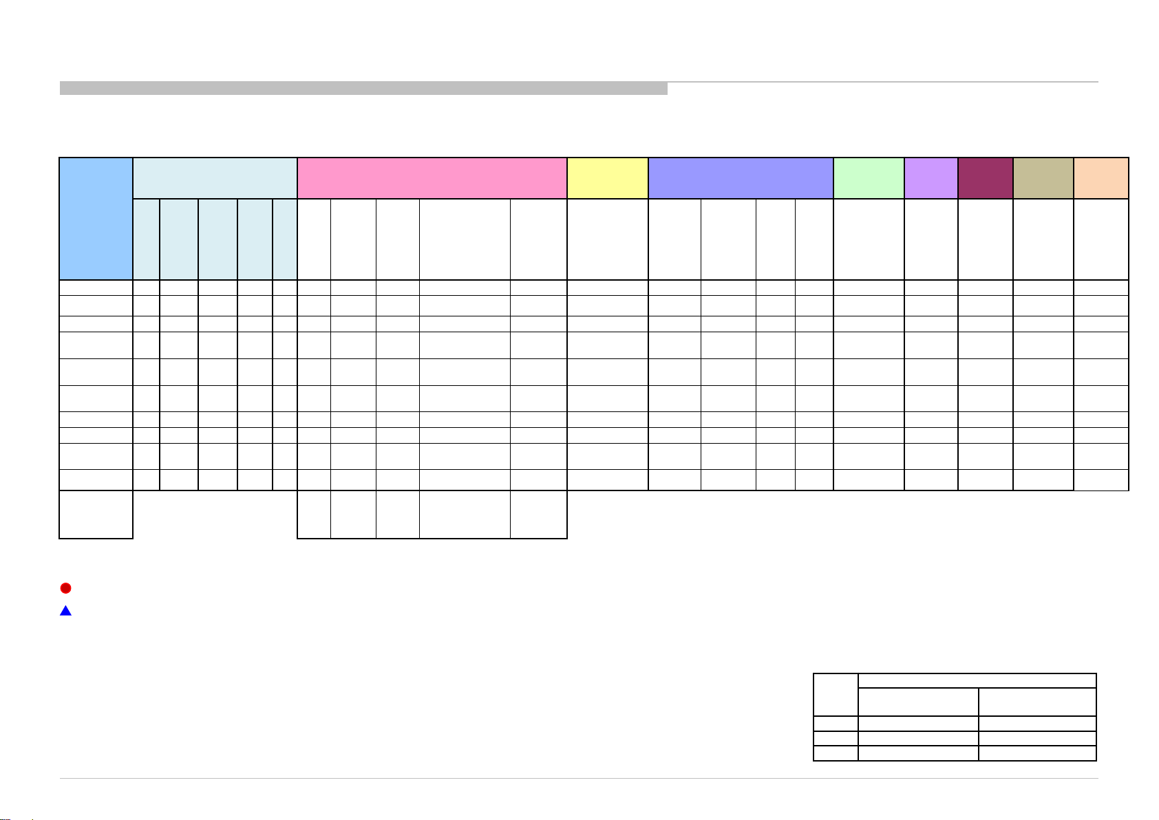
2-5. Triage Chart
(missing/
distorted)
Stationary
dots
Cannot
(Tact-Key OK)
Segment
Reference
QT QW QW-L SE3N SE3 2 3 4 5 6
Symptoms - Shutdown. Power LED
blinking red diagnostics sequences
B* Board Y Y Y Y Y
AC Adaptor Y Y Y Y Y
H* Board Y Y Y Y Y
Stereo
Speaker
Assist
Speaker
Wi-Fi
module
Y Y Y Y Y
Y Y
Y Y Y
LVDS FFC Y Y Y Y Y
LED Panel Y Y Y Y
Tuner
module
Y Y Y Y Y
Switch Unit Y Y Y Y Y
Problem
Power Audio
No Power
(No Pic, No
Sound, No BL)
No Power LED
&
No Reponse to
remote
(Dead Set)
colored
lines or
Video
(missing/distorted)
No Video
in 1(one)
of Inputs
No
Video
in
All
Inputs
RF
Tune
Remote
No Reponse
when press
remote key
Panel
(Power)
Panel
(Communication)
Panel
(Backlight)
Network
*QT,QW,
SE3N
Wireless
can't
connect
Audio
No Audio
front LED Tact-Key
No
No LED
(Set is still
alive)
Response
when
press
Tact-Key
(Remote
OK)
Most likely defective part
Secondary possible defective part
B* Board Type
Size
PAN ASIA,AMERICA,
CHINA
EUROPE
32” BBA BBE
40” BBA BBE
48” BBA BBE
11
Page 12
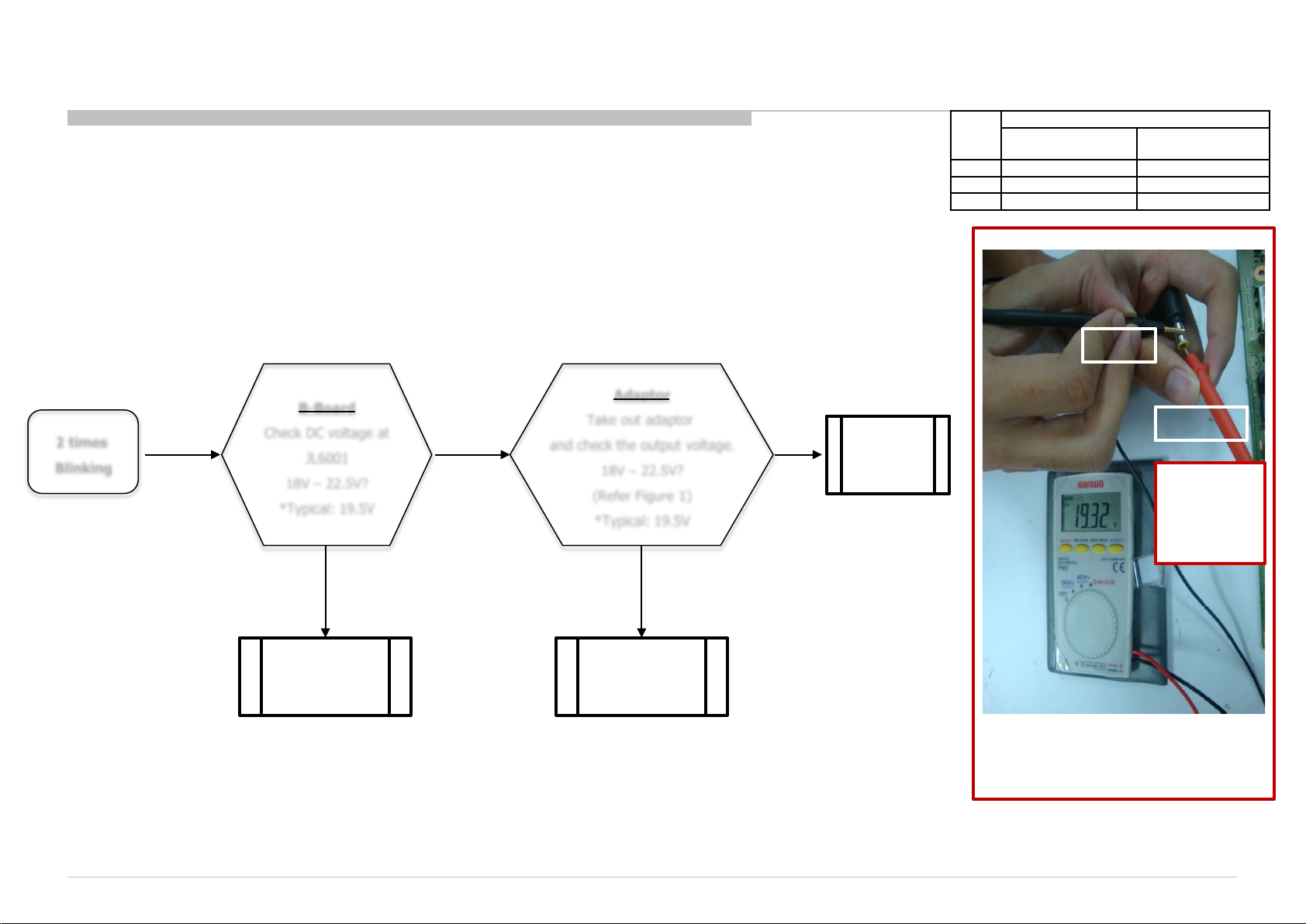
3-1. LED BLINKING
3-1-1. 2x Blinking (Main power Error)
BBE, BBA board (QW, QWL) only
SECTION 3
TROUBLESHOOTING
B* Board Type
Size
PAN ASIA,AMERICA,
CHINA
32” BBA BBE
40” BBA BBE
48” BBA BBE
-ve
EUROPE
2 times
Blinking
B-Board
Check DC voltage at
JL6001
18V – 22.5V?
*Typical: 19.5V
Yes
Change B-board Change B-board
No
and check the output voltage.
Adaptor
Take out adaptor
18V – 22.5V?
(Refer Figure 1)
*Typical: 19.5V
Yes
No
+ve
Change
adaptor
Ensure that
+ve probe is
touching the
needle.
Figure 1: How to check adaptor’s output
voltage.
12
Page 13
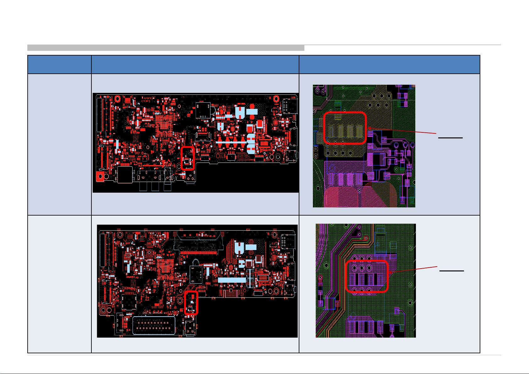
2 x Blinking (Checking Point)
Board Name Board PWB (A side) Detail
BBA
(Q6020)
Q6020
BBE
(Q6020)
Q6020
13
Page 14
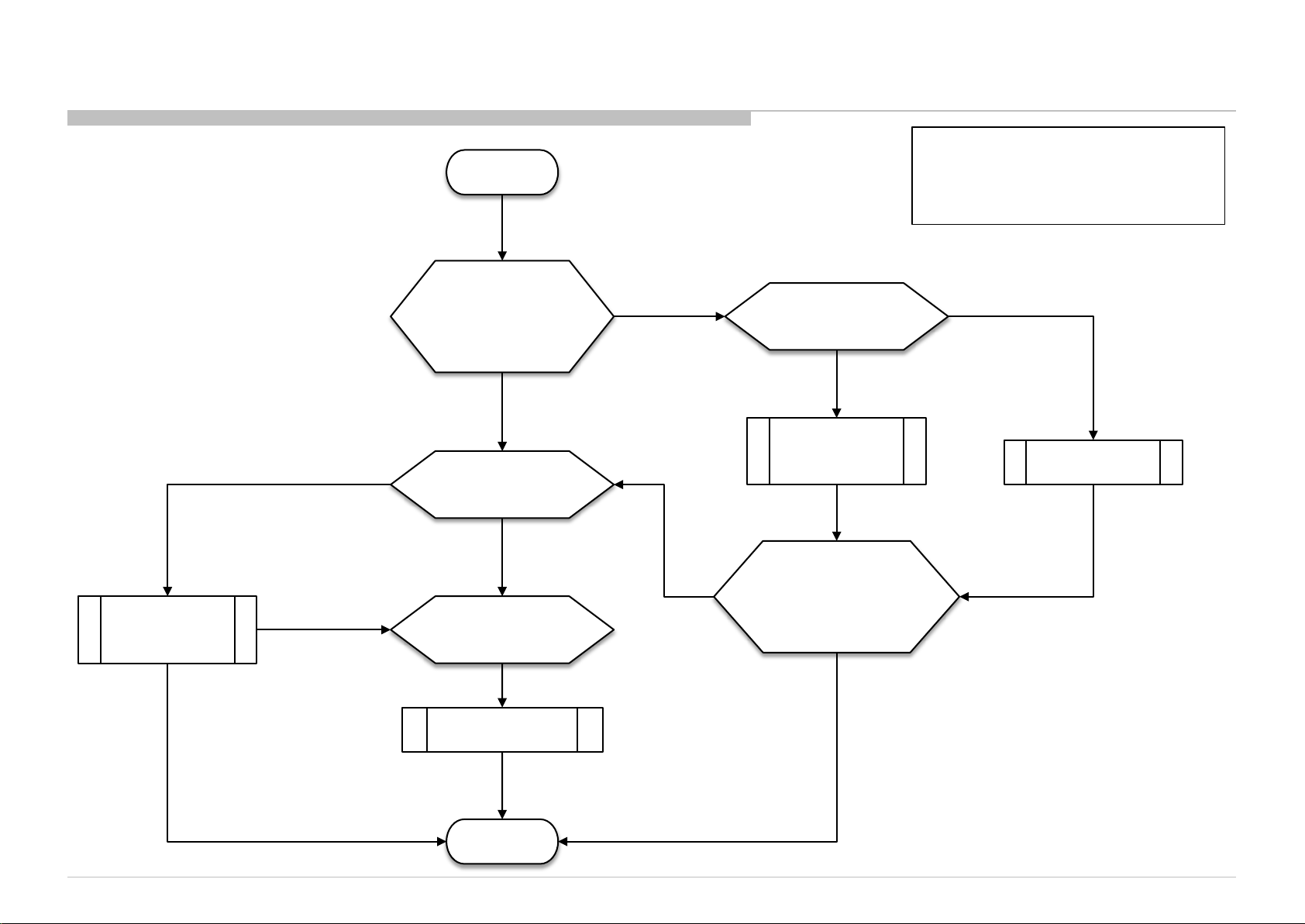
3-1. LED BLINKING
3-1-2. 3x Blinking (Audio Error)
START
3x blinking
TV must be power OFF condition
before unplug any of the
FFC/FPC/wire/cable from the board.
-> This is to prevent possibility
circuit damage happen.
No connectivity of F4000
F4000 broken,
Replace F4000
3x blinking
Remove
Speaker Connector
at CN4001 & perform
AC OFF - ON
3x blinking
Check connectivity
of F4000
3x blinking &
F4000 OK
Audio IC problem,
IC4001 damage
No 3x blinking
3x blinking
Check Speaker harness
And Speaker impedance
No connectivity for
speaker harness
Change Speaker
Harness
Connect back
Speaker Connector
to CN4001
& perform AC OFF - ON
Speaker Impedance
≠ 6~8 Ω
Change Speaker
No 3x blinking
Change BB* board
No 3x blinking
DONE
14
Page 15
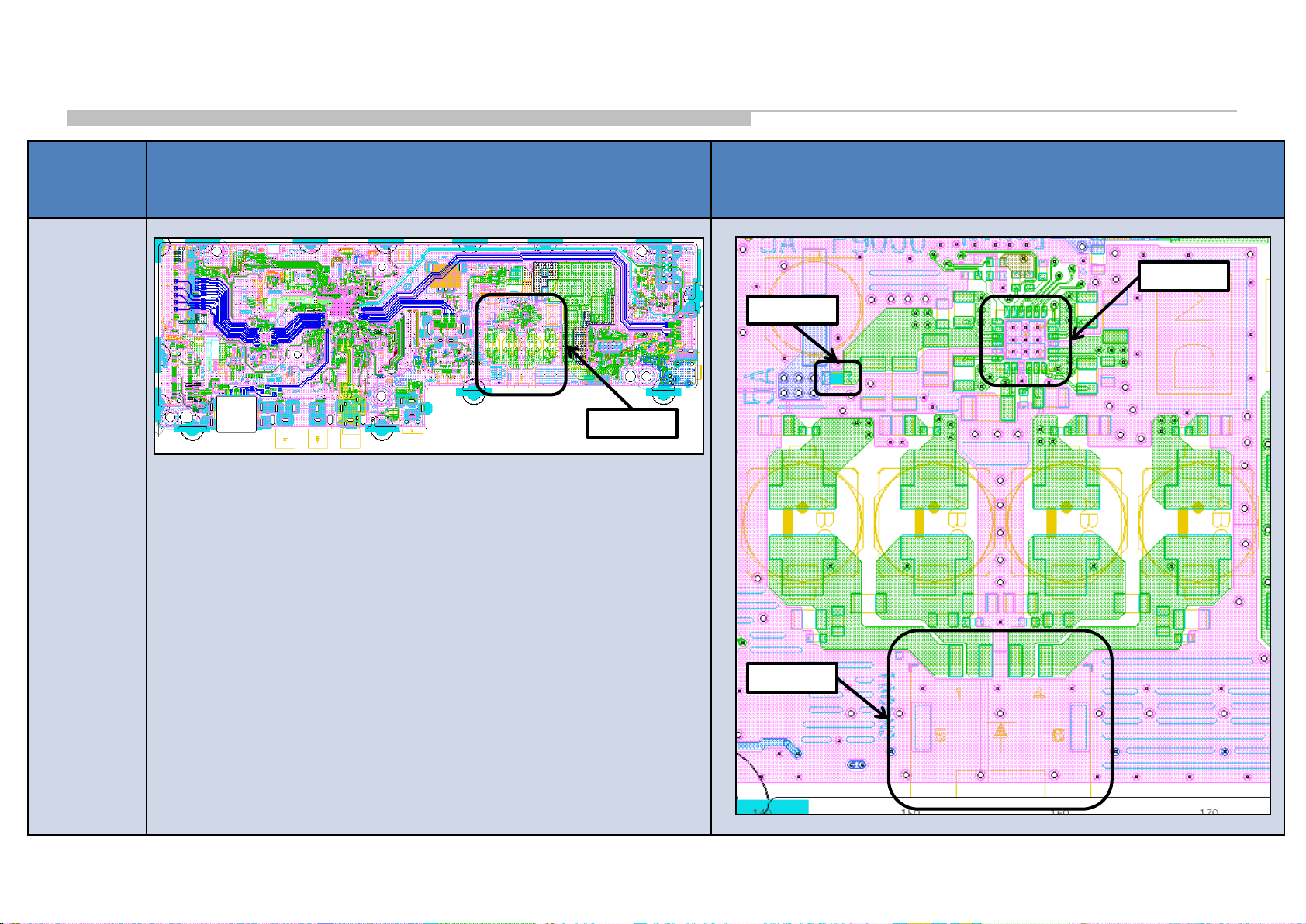
3x Blinking (Checking Point)- BBA
Board
Name
BBA
(QW, QT)
IC4001
F4000
CN4001
Board PWB (A side) Details
IC4001
F4000
Details
CN4001
15
Page 16
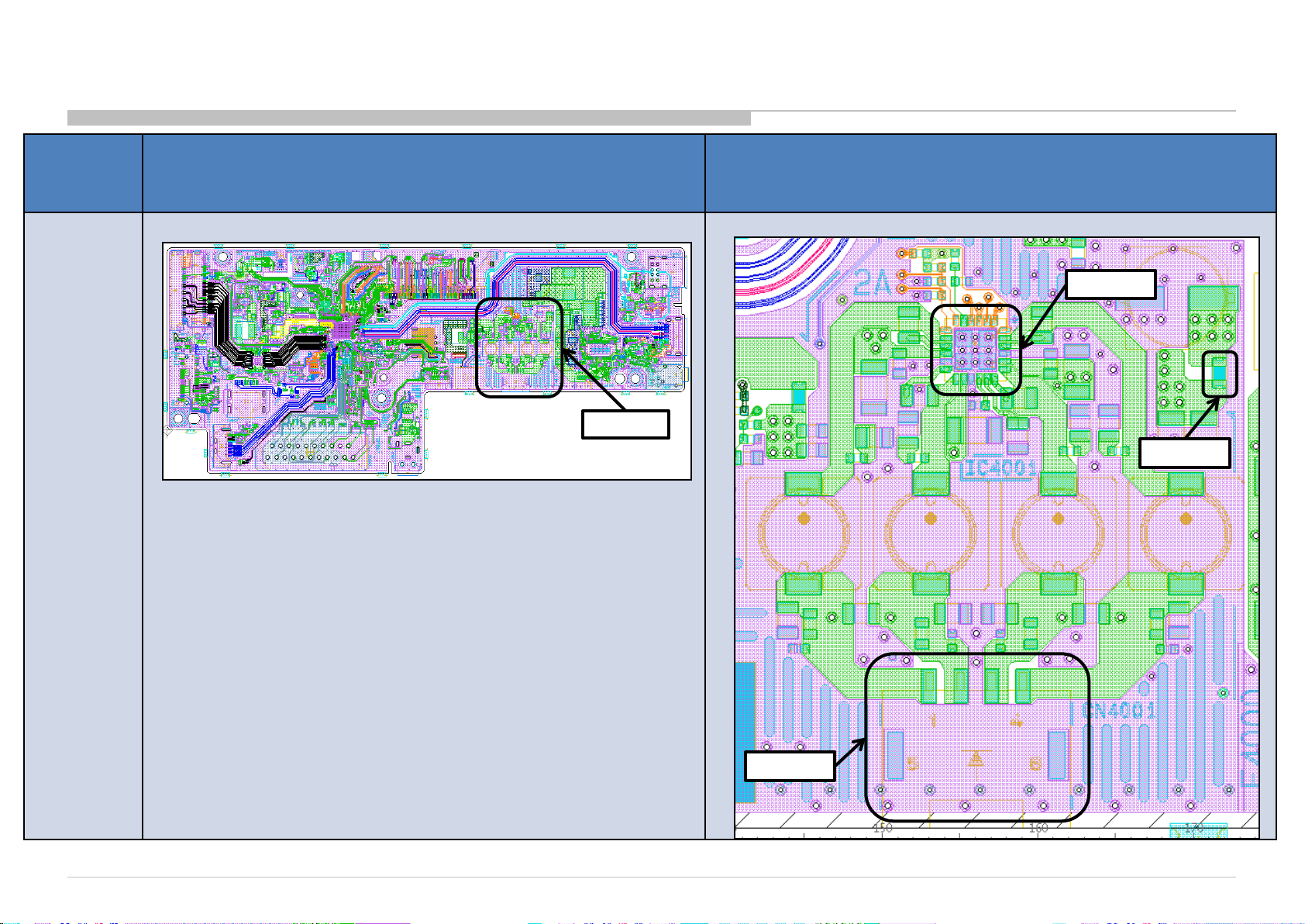
3x Blinking (Checking Point)- BBE
Board Name Board PWB (A side) Details
BBE
(QW, QWL,
QT)
IC4001
F4000
CN4001
Details
IC4001
F4000
CN4001
16
Page 17
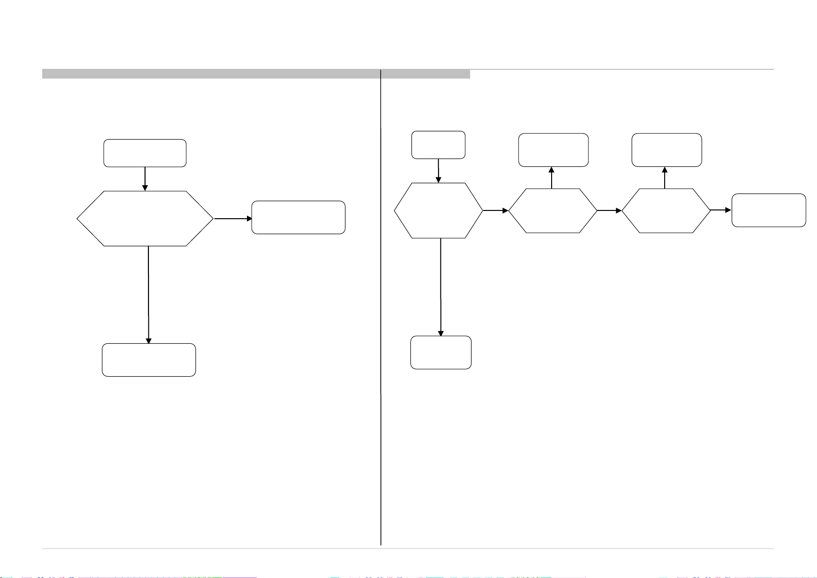
3-1. LED BLINKING
3-1-3. 4 x Blinking (Panel Power Error)- BBA
3-1-4. 4 x Blinking (Panel Power Error)- BBE
Start
Check voltage at
JL6030(BBA)
11.52V-12.82V?
Yes
End
No
IC6019 Checking
Procedure
Start
Check voltage at
JL6034(BBE)
11.52V-12.82V?
Yes
End
MTK Problem
or TV in stand-
No
Check PANEL_PWR
3.00V-3.33V?
by mode.
No
Yes
Check JL6034 (BBE)
11.52V-12.82V?
Replace
Q6023
Yes
No
Refer IC6019
Checking
Procedure
17
Page 18
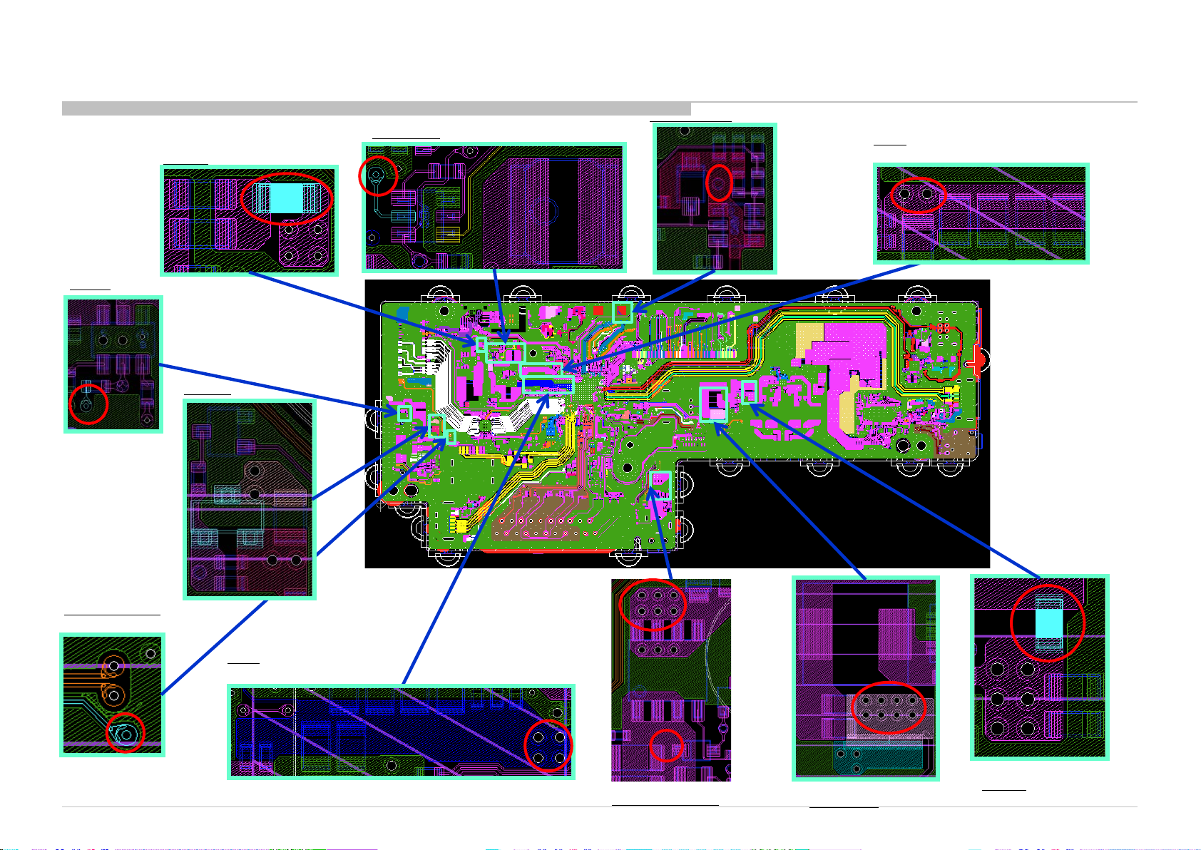
4 x Blinking (Checking Point) QW/QT-BBE [1/2]
POWER1
F6003
EN_V
Q6023
3.3V_STBY
1.5V
PANEL_PWR
1.2V
19.5V
Q6020
19.5V_ADP
19.5V & Q6020
F6002
STBY_5V
18
Page 19
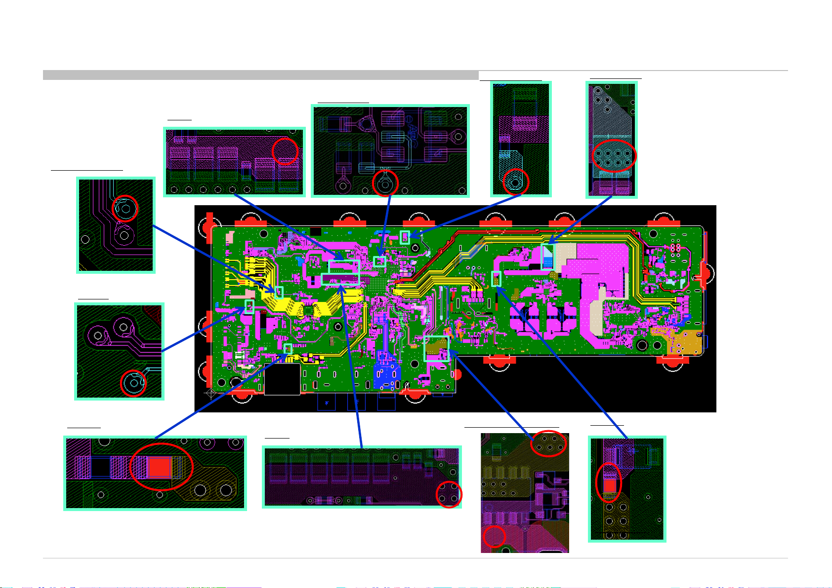
4 x Blinking (Checking Point) QW/QT –BBA [2/2]
1.5V
PANEL_PWR
EN_V
POWER1
3.3V_STBY
STBY_5V
F6003
1.2V
19.5V & Q6020
19.5V
Q6020
19.5V_ADP
F6002
F6002
19
Page 20
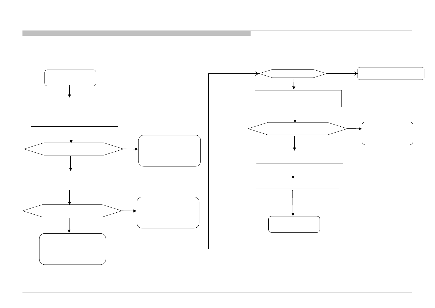
3-1. LED BLINKING
3-1-5. 5 x Blinking (Panel I2C Error - General Checking)
START
Reinsert LVDS Flat
Flexible Cable (FFC) at B-Board
and Panel Side. Make sure FFC is
taped properly.
5 Times Blinking happen?
YES
Replace LVDS Flat Flexible
Cable (FFC)
5 Times Blinking happen?
YES
Check voltage PANEL_SDA &
PANEL_SCL.
Is 3V available?
No
No
TV set is OK now
NG Symptom:
Incorrect FFC Insertion
TV set is OK now
NG Symptom:
LVDS Cable NG
Is 3V -3.33V available?
YES
Replace
O-Cell* or Panel Module*
5 Times Blinking happen?
YES
Replace B-Board
TV Boots Up Normally
END
NO
No
Refer to Panel I2C
Manual Checking
TV set is OK now
NG Symptom:
B-Board Issue NG
* O-Cell or Panel
Module
replacement
depends on
service
capabilities
20
Page 21
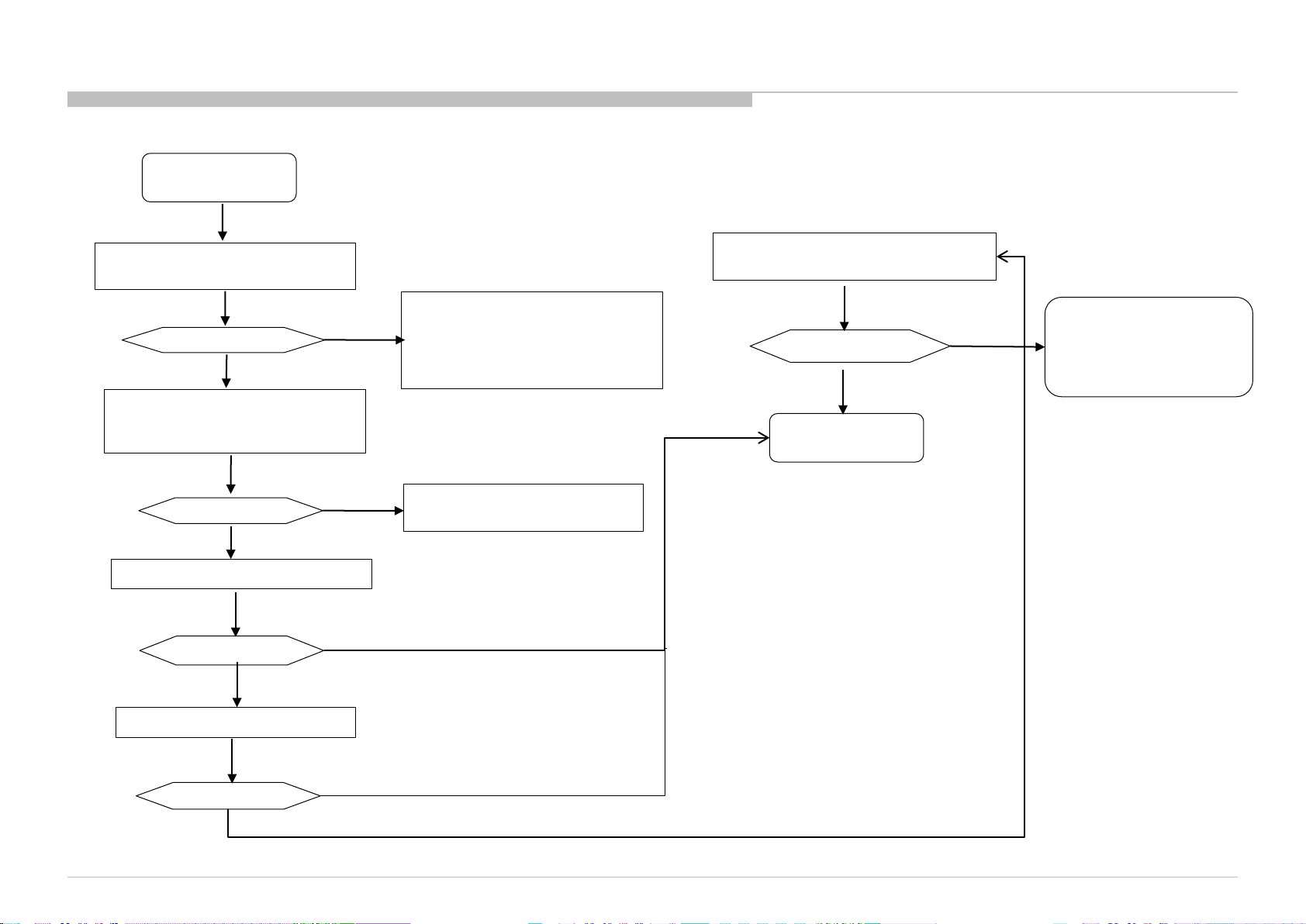
3-1. LED BLINKING
3-1-6. 5x Blinking (Panel I2C Checking Manual)
START
Check Impedance at PANEL_SDA &
PANEL_SCL.
Is High Impedance?
Yes
Check voltage 3.3V at
Q8601 (Source).
3V available?
Is 3V-3.33V available?
YES
Replace Q8601
5 Times
Blinking happen?
Yes
No
No
NO
Suspect IC5000/IC5001/IC9000 NG
IC9000 – Refer to 6X Blinking
IC5001 – Refer to No Picture
Troubleshooting
IC5000 – Replace Board
DDCON checking procedure
(IC6009)
Check CN8600 (32”F/40”/43”/ 48”/49”)
or CN8601 (32”W) condition.
NO
Is Connector OK?
YES
END
Replace CN8600/CN8601
NG Symptom:
CN8600/CN8601 Mount
or Part Issue
Replace Q8600?
5 Times
Blinking happen?
Yes
No
21
Page 22
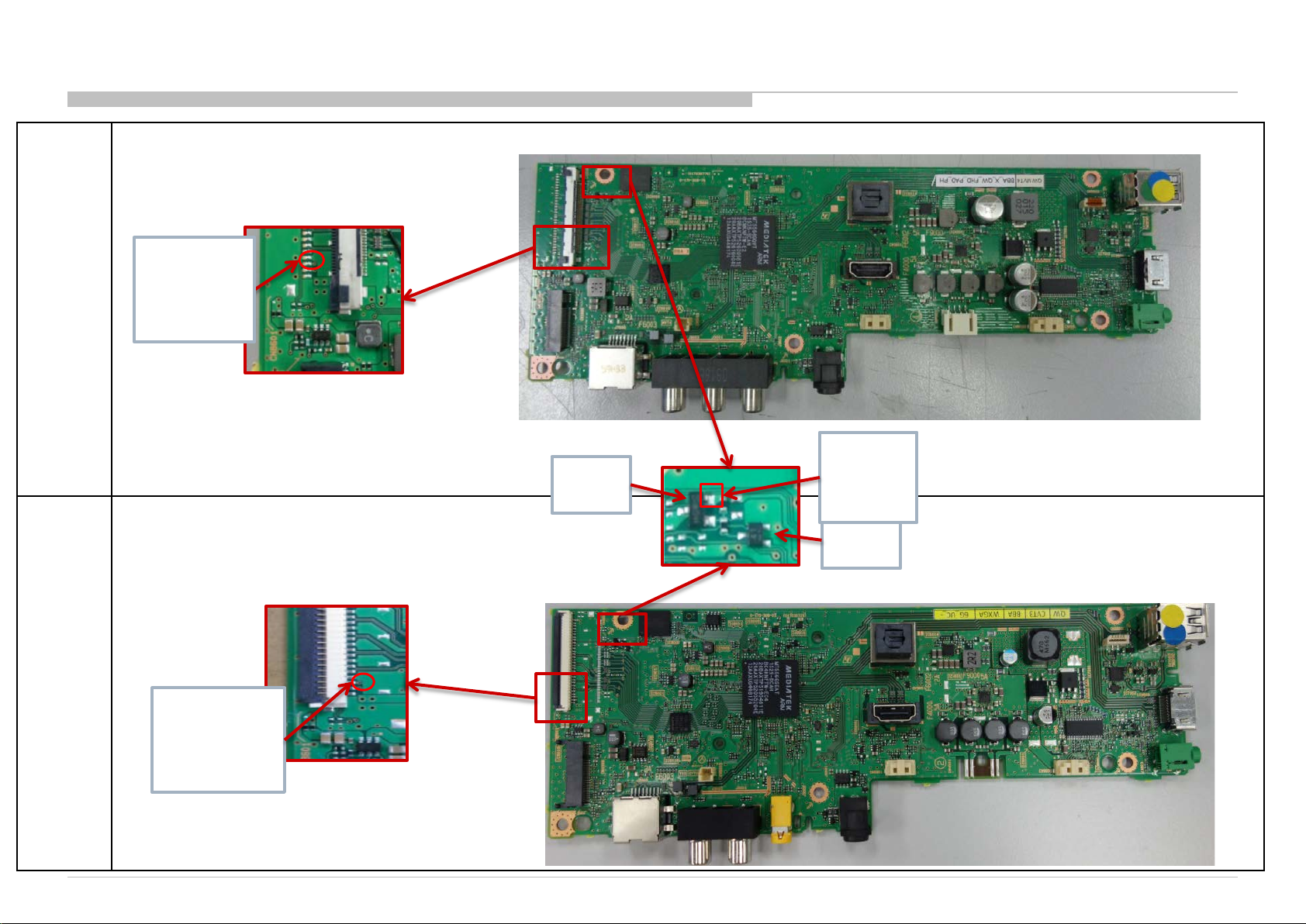
5 x Blinking (checking Point [1/2])
BBA
FHD
PANEL_SD
A (Top)
PANEL_SC
L (Bottom)
BBA
WXGA
Q860
1
Q8601
(Source
)
Q860
0
PANEL_SDA
(Top)
PANEL_SCL
(Bottom)
22
Page 23
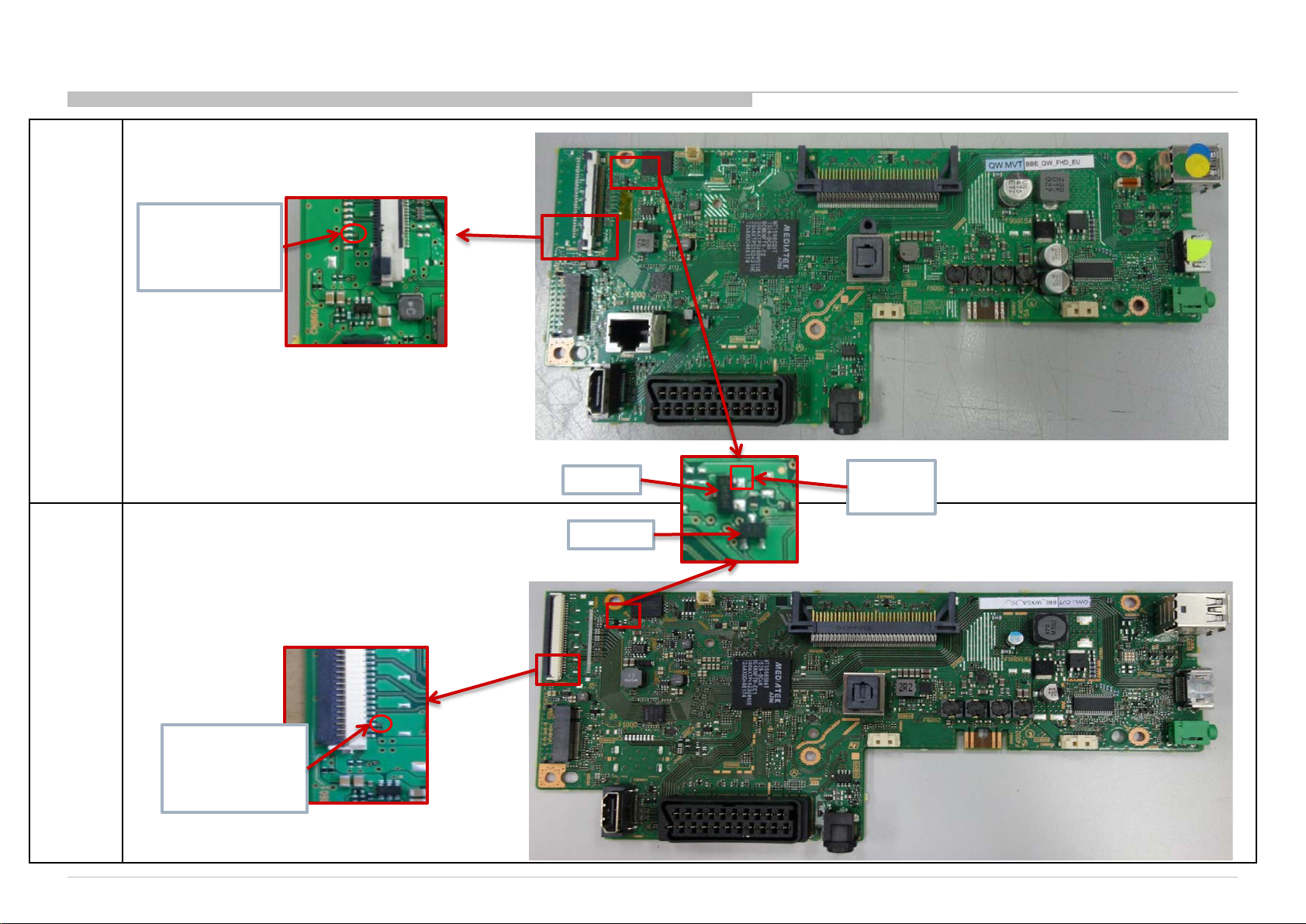
5 x Blinking (Panel I2C Checking Manual [2/2])
BBE
FHD
PANEL_SDA
(Top)
PANEL_SCL
(Bottom)
BBE
WXGA
PANEL_SDA
(Top)
PANEL_SCL
(Bottom)
Q8601
Q8600
Q8601
(Source)
23
Page 24
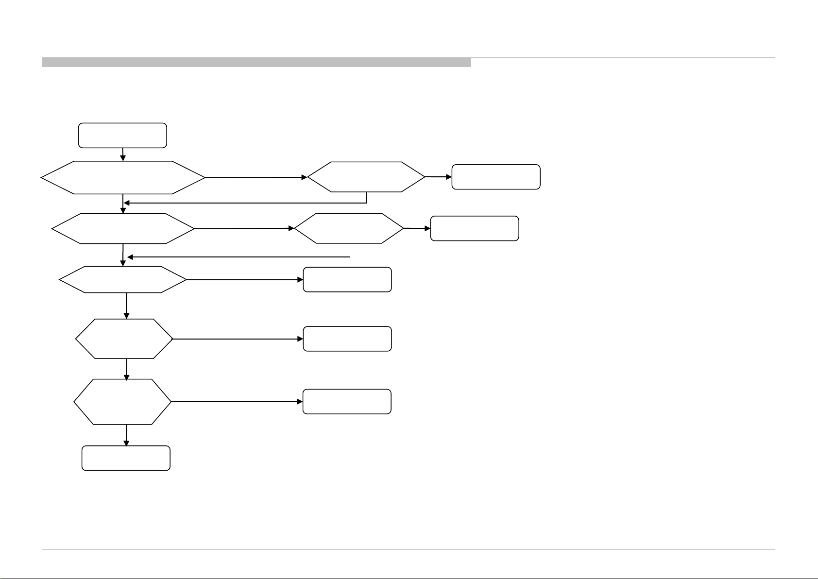
3-1. LED BLINKING
3-1-7. 6x Blinking (Backlight Error)- QW
6x Blinking
Check if LED harness (CN9000)
is connected properly?
Yes
Check F9000 Fuse.
Impedance fuse > 1Ω?
No
Change B Board.
AC ON 6x Blinking?
Yes
Able to repair
Panel Module?
Yes
Change Harness.
AC ON 6x Blinking?
Yes
Replace LS bar*
No
Yes
Yes
Yes
No
No
No
Connect LED harness
AC ON 6x Blinking?
Change F9000 Fuse.
AC ON 6x Blinking?
B Board broken**
Change Panel Module
Harness broken
No
No
LED harness loose
Fuse F9000 broken
*To avoid changing all LS bar, please follow steps below
(1) Turn off AC
(2) Unplug DC adaptor from DC jack
(3) Plug in DC adaptor to DC jack
(4) Turn on AC
(5) LS bar will turn on for ~4s before 6x blinking
(6) Observe which LS bar cannot turn on during power on
(7) Replace LS bar that failed to turn on
**For 6x blinking B Board Troubleshooting please refer
next page.
24
Page 25
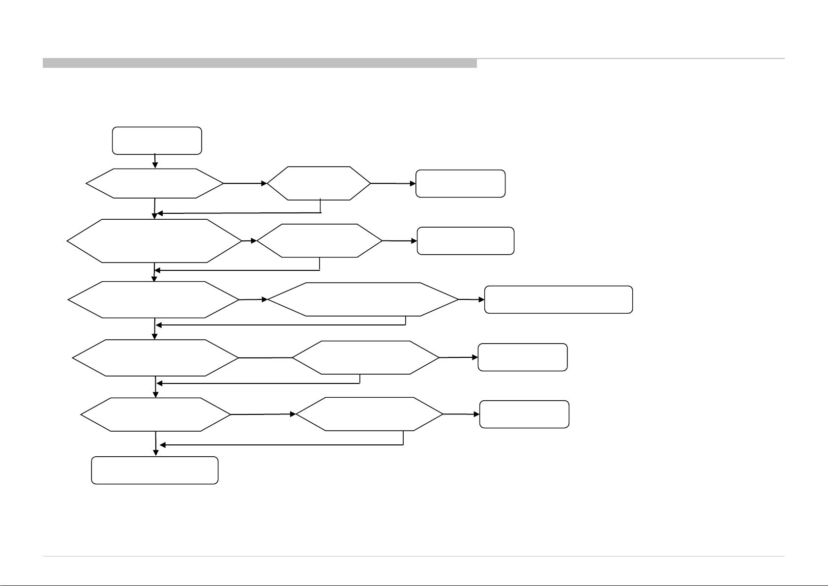
3-1. LED BLINKING
3-1-8. 6x Blinking (Backlight Error - B Board Troubleshooting)-QW
B-Board Broken
Check D9001 (AC OFF)
VF > 0.1V and < 0.8V?
Yes
Check LED_VCC (AC OFF)
LED_VCC short to ground?
Impedance > 1kΩ?
Yes
Check D9002 (AC OFF)
VF > 0.5V and < 1V?
Yes
Check L9001 (AC OFF)
L9001 impedance < 1Ω?
Yes
Check Q9000 (AC OFF)
Impedance RDS > 100 ohm
Yes
No
Yes
No
Yes
No
Yes
No
Yes
No
Yes
Change D9001.
AC ON 6x Blinking?
Change C9026 & C9027
AC ON 6x Blinking?
Change D9002, Q9001, and RB9001
AC ON 6x Blinking?
Change L9001
AC ON 6x Blinking?
Change Q9000
AC ON 6x Blinking?
No
No
D9001 broken
C9026 & C9027 broken
No
D9002, Q9001, and RB9001 broken
No
No
L9001 broken
Q9000 broken
Suspect : Other Part damage
Change the board
25
Page 26
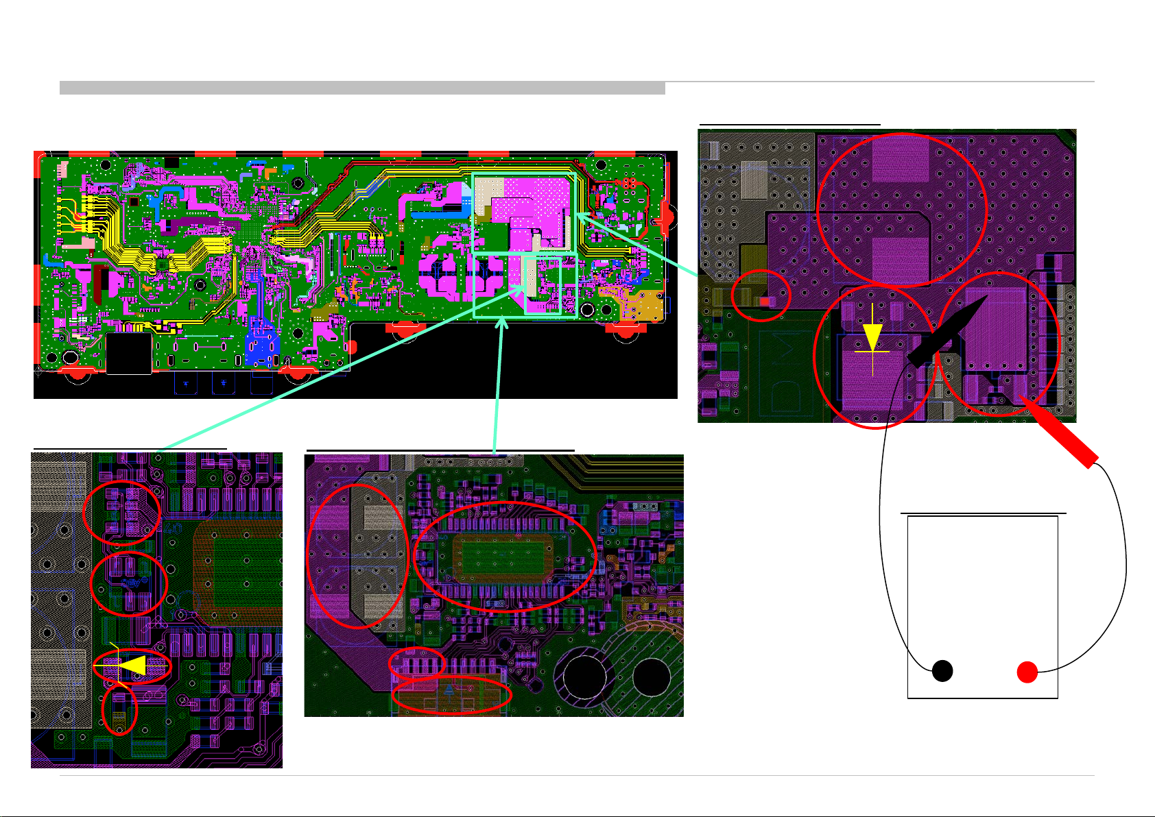
6x Blinking (Checking Point) QW-BBA [1/2]
F9000, L9001, D9001, Q9000
L9001
F9000
S
Q9000
D9001
D
RB9001, Q9001, D9002, R9021
RB9001
Q9001
D9002
R9021
C9026, C9027, CN9000, IC9000, LED_VCC
C9026
IC9000
C9027
LED_VCC
CN9000
Q9000 RDS Measurement
Multimeter
-ve
+ve
26
Page 27
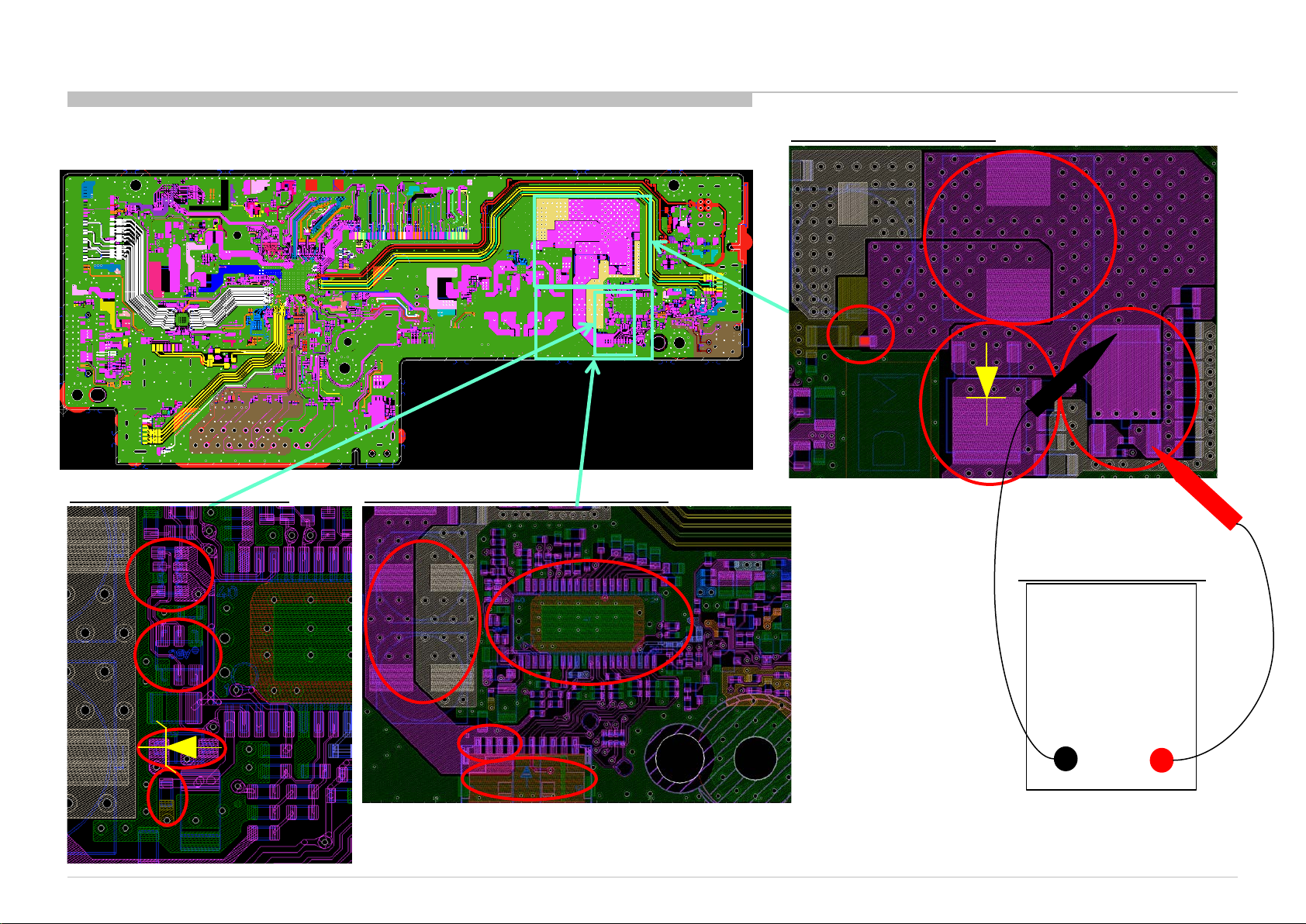
6x Blinking (Checking Point) QW-BBE [2/2]
F9000, L9001, D9001, Q9000
L9001
F9000
S
Q9000
D9001
D
RB9001, Q9001, D9002, R9021
RB9001
Q9001
D9002
R9021
C9026, C9027, CN9000, IC9000, LED_VCC
C9026
IC9000
C9027
LED_VCC
CN9000
Q9000 RDS Measurement
Multimeter
-ve
+ve
27
Page 28
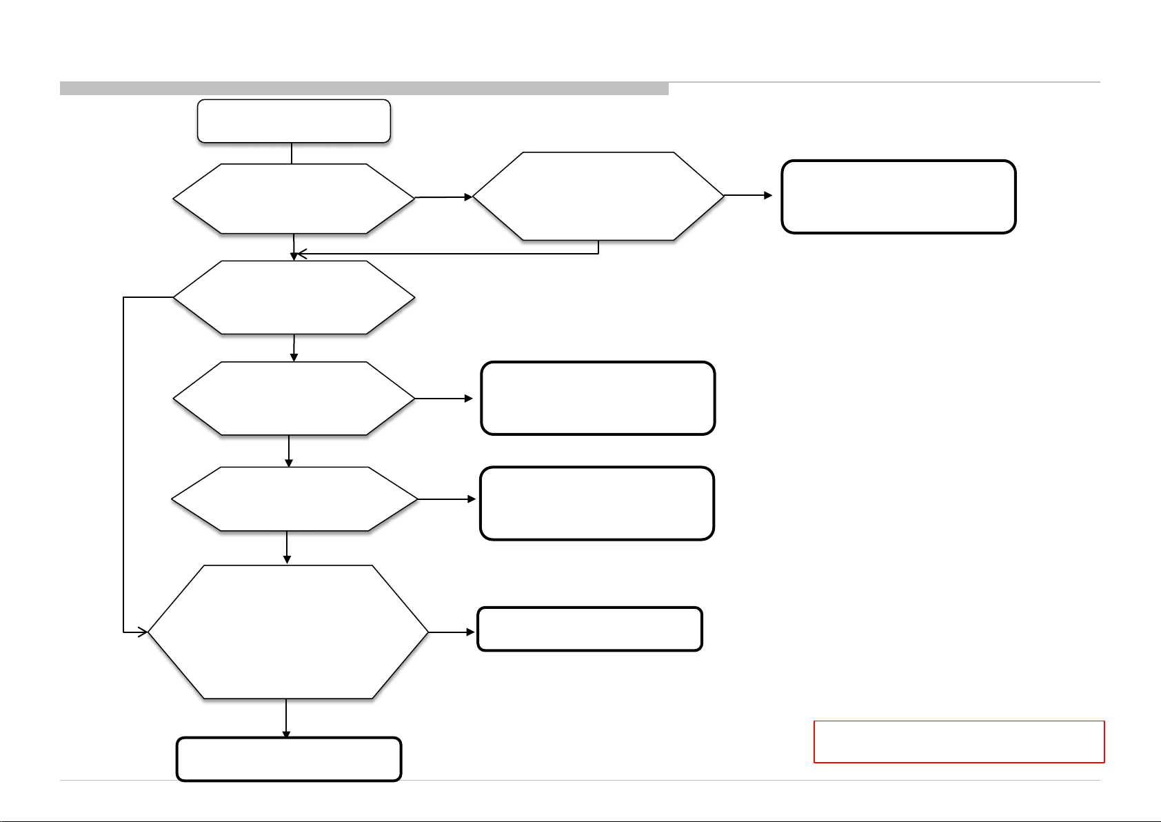
3-2. NO POWER
3-2-1.H-board troubleshooting flow (for QW, QWL)
TV cannot be controlled
by remote commander
Yes
Check Green LED
at Power LED indicator.
Is it lighted up?
No
Check voltage at
Pin1 of H board connector
(refer next page)
Is it 5V?
No
Check H board to B board
harness condition.
Is it connected properly?
Yes
Check voltage at resistor of
5V source of B board.
Is it 5V?
Yes
No
Yes
No
Place remote commander (RC)
near to window and press RC key.
Is the LED blinking?
No
Connect harness properly
STBY5V NG. Refer toIC6014
troubleshooting section
Yes
Change Mechanical part
(ex. Ornamental panel,
or guide light)
Check SIRCS voltage
using multimeter
at R5038 on B board.
Then press and hold RC key and
observe voltage drop.
Does it drop
from 3.9V to (<2.9V)?
Yes
Main IC SIRCS line broken.
Change B-board
No
IR sensor broken.
Change H board.
Condition: TV is plugged to AC power supply,
and AC power supply is turned ON.
28
Page 29
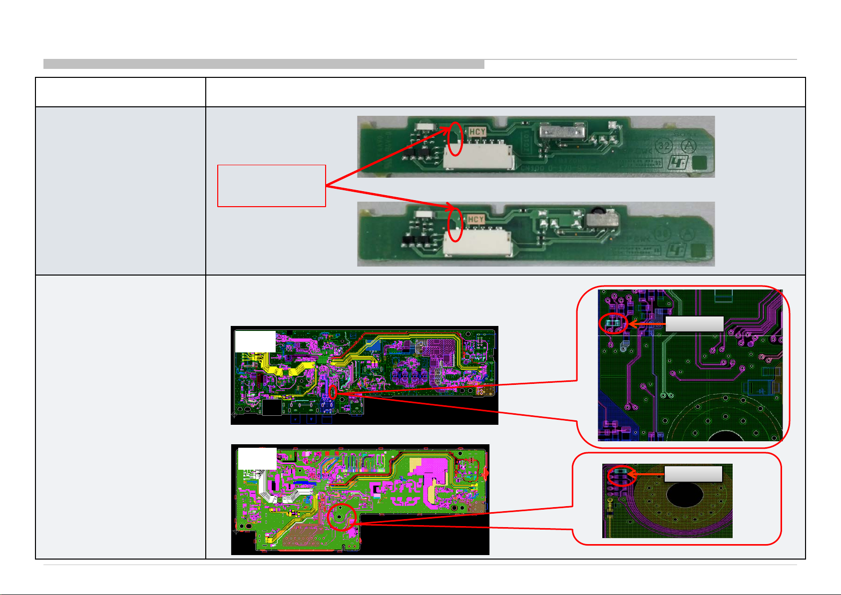
H-board troubleshooting flow (Checking Point)
Board name Board picture
HCY
Pin 1 of
H board connector
B board
R5038
BBA
BBE
R5038
29
Page 30
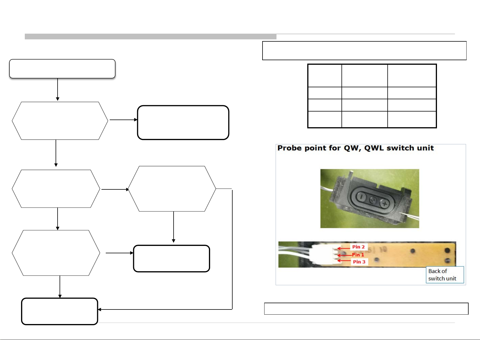
3-2. NO POWER
3-2-2 : Switch unit troubleshooting flow (for QW, QWL)
Switch Unit NOT FUNCTIONING
Check if Wire Harness
And Connector is
connected properly?
Yes
** Check 3.3V
in Pin2, CN1
(Switch Unit).
Is it 3.3V?
No
No
Change Wire Harness
And connect properly
**Check 3.3V in (Pin
8, CN9702 on
B board . Is it 3.3V?
*VOLTAGE LEVEL FOR EACH PRESSED BUTTON (for QW, QWL, QT
switch unit only)
KEY Voltage
(average)
+
No Input
0.000
1.05
2.420
Voltage
range
0.00 – 0.2
1.00 – 1.13
2.26 – 2.58
Yes
*Check Pin 1
Voltage Level in CN1
(switch unit). Is
voltage level
according to key
pressed?
Yes
Change B-board
Yes
NG
Change Switch Unit
No
**see next page for probing point of B board
30
Page 31
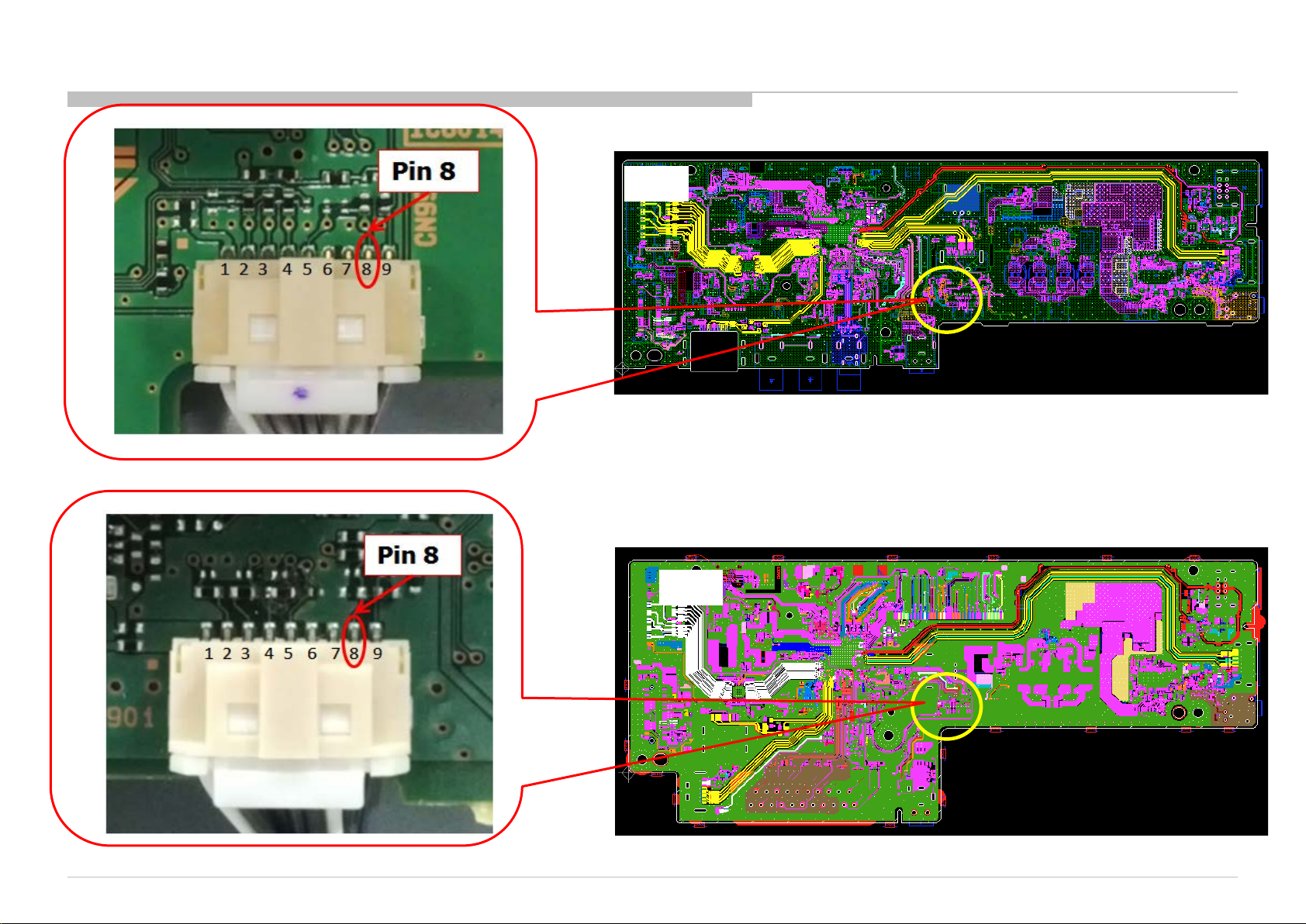
BBA
Pin 8
BBE
31
Page 32
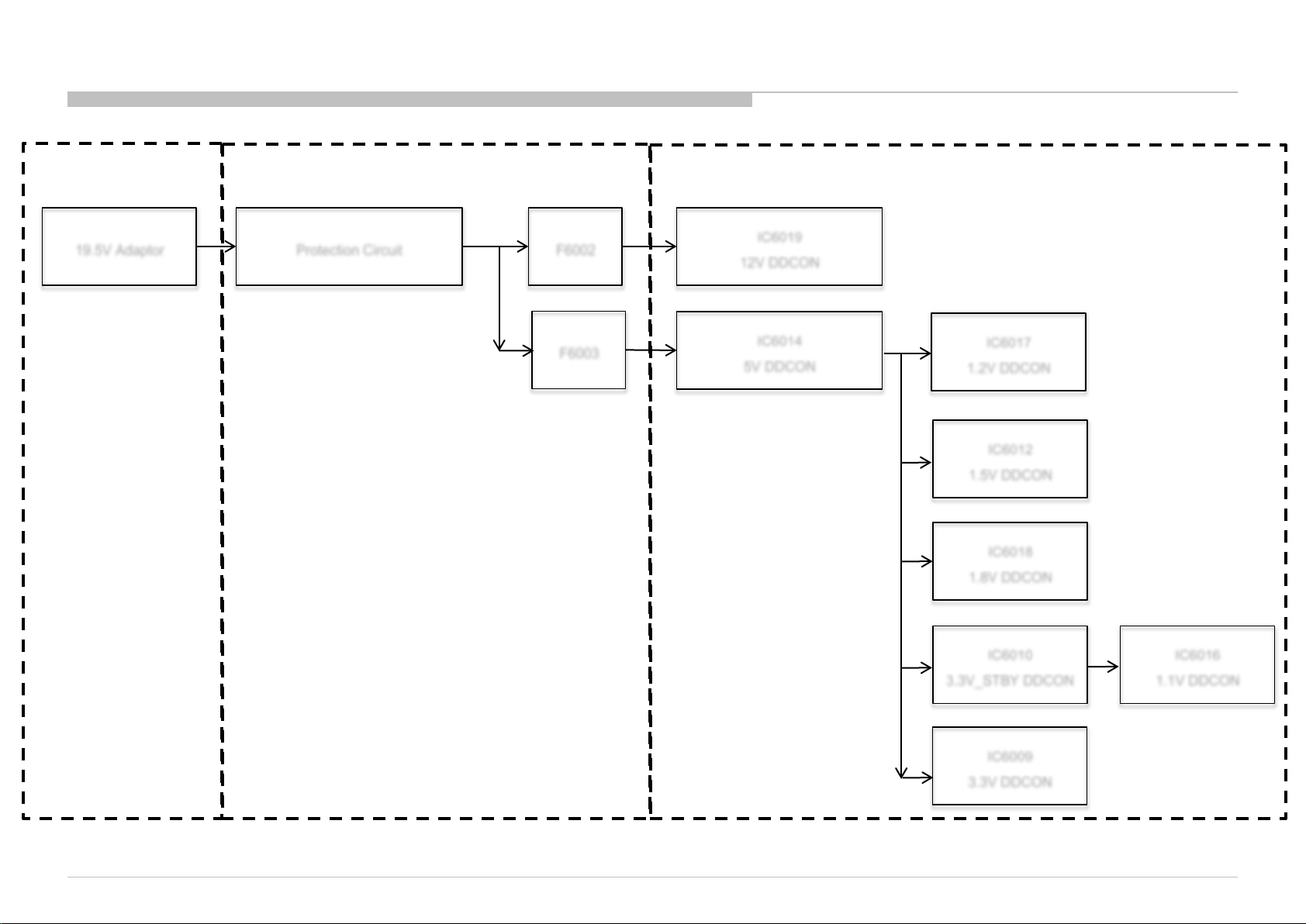
3-2-3. DC-DC Converter Basic Block Diagram
Input Circuit
Side
19.5V Adaptor
Protection Circuit
Protection Circuit
Side
F6002
F6003
IC6019
12V DDCON
IC6014
5V DDCON
DDCON
Side
IC6017
1.2V DDCON
IC6012
1.5V DDCON
IC6018
1.8V DDCON
IC6010
3.3V_STBY DDCON
IC6009
3.3V DDCON
IC6016
1.1V DDCON
32
Page 33
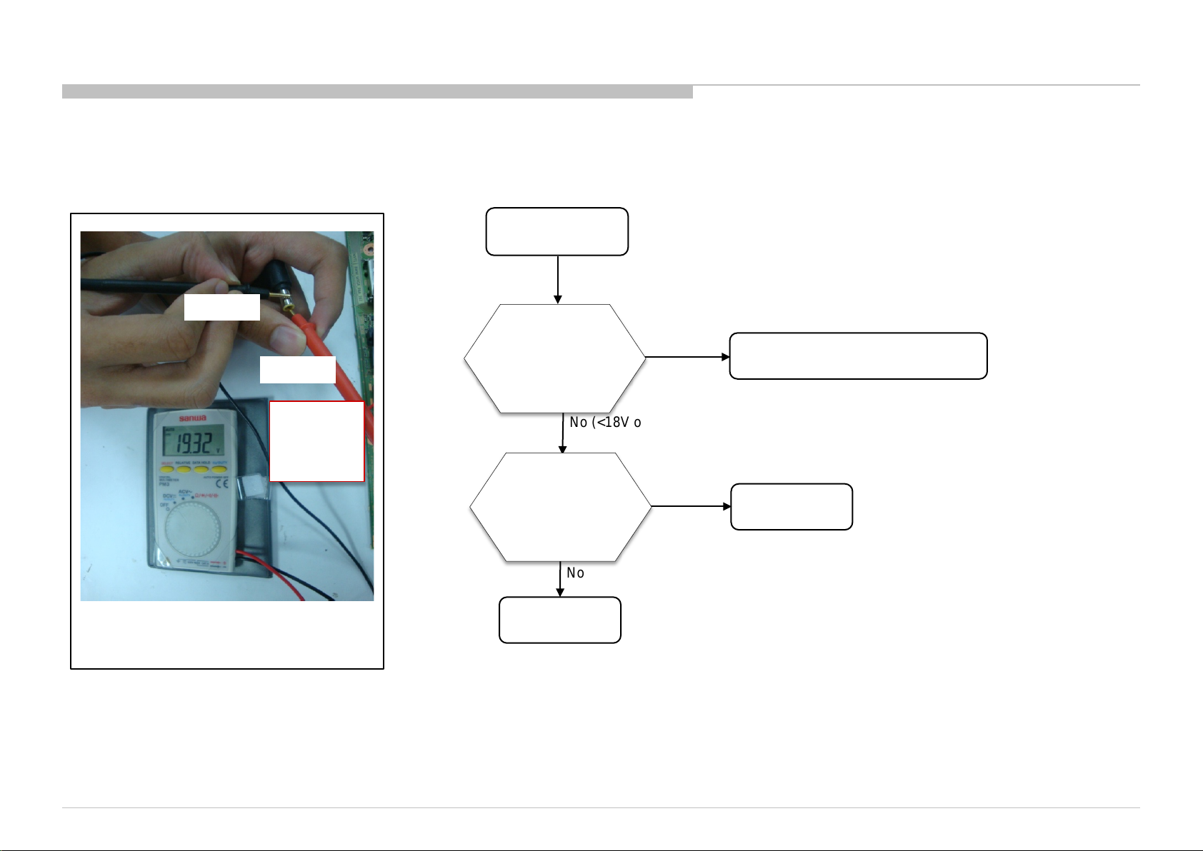
3-2-4. Adaptor Checking Procedure
Start
-ve
+ve
Ensure that
+ve probe is
touching the
needle.
Figure-1: How to check adaptor’s output
voltage.
Take out adaptor.
Check the output voltage.
18V – 22.5V?
(Refer Figure-1)
No (<18V or >22.5V)
Change adaptor.
Check the output voltage.
18V – 22.5V?
(Refer Figure-1)
No
AC Source
Yes
Yes
Refer ‘Protection Circuit -
Checking Procedure -next page.
Adaptor
33
Page 34

3-2. NO POWER
3-2-5. Protection Circuit– Checking Procedure
Refer
Adaptor Checking Procedure
Start
B-Board
Check voltage at
Q6020 (PIN5-PIN8)
18V-22.5V?
YES
Refer
‘No Power -DDCON Checking Procedure’
NO (0V)
B-Board
Check voltage at
Q6020 (PIN1-PIN3)
18V-22.5V?
NO
B-Board
Remove Q6020 &
Check 19.5V_ADP line by
continuity test.
Short or OK?
OK
YES
SHORT
B-Board
Check voltage at Q6020 – PIN4
9V–11V or 18V–22.5V?
18V–22.5V
J6001 or Q6019 damage or
Adaptor not inserted properly
B-Board
Remove J6001 &
Check 19.5V_ADP line by
continuity test.
Short or OK?
OK
9V–11V
SHORT
B-Board
Replace Q6020 &
Check voltage at
Q6020 (PIN5-PIN8)
18V-22.5V?
NO
Refer
‘Fuse Checking Procedure’
Check & remove any foreign material
Check 19.5V_ADP line by
B-Board
On the board.
continuity test.
Short or OK?
OK
YES
Q6020 Damage
SHORT
PWB
Refer
Adaptor Checking Procedure
J6001 Damage
Foreign Material
34
Page 35
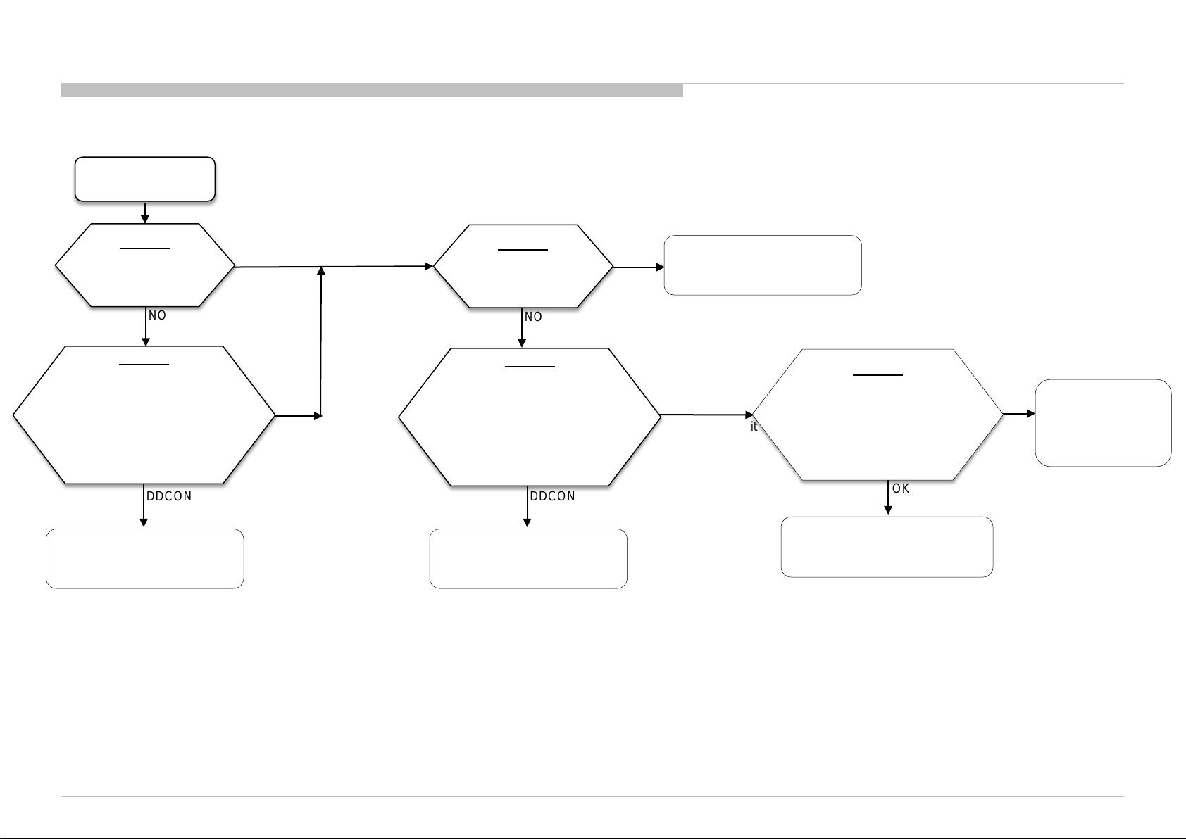
3-2-6. Fuse Checking Procedure
Start
B-Board
Check F6002 by
Continuity Test.
NO
B-Board
Replace F6002 & check
continuity test at both
F6002 terminals.
Short at ‘Protection Circuit’ side
or ‘DDCON’ side?
DDCON
Refer No Power -DDCON
Checking Procedure.
OK
Protection Circuit
B-Board
Check F6003 by
Continuity Test.
NO
B-Board
Replace F6003 & check
Check continuity test at both
F6003 terminals.
Short at ‘Protection Circuit’ side
or ‘DDCON’ side?
DDCON
Refer No Power -DDCON
Checking Procedure.
OK
Refer DDCON
Checking Procedure.
Protection Circuit
B-Board
Check & remove any foreign material
On the board.
Check 19.5V line by continuity test.
Short or OK?
OK
Foreign Material
NO
Refer
Audio & LED Driver
Checking Procedure
35
Page 36
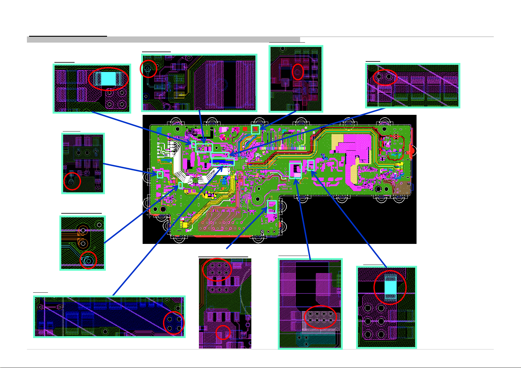
Checking Point - BBE
F6003
EN_V
PANEL_PWR
3.3V_STBY
POWER1
1.5V
1.2V
19.5V & Q6020
19.5V
Q6020
19.5V_ADP
STBY_5V
F6002
36
Page 37
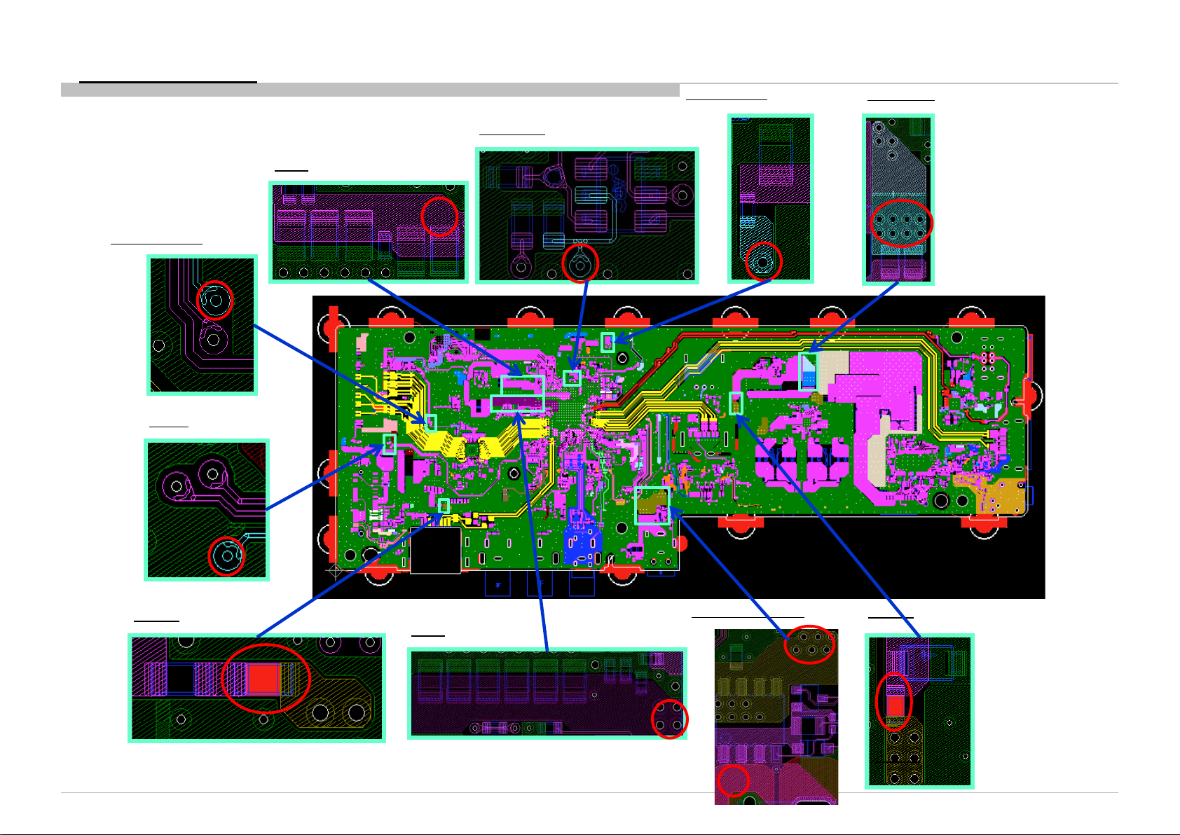
Checking Point - BBA
PANEL_PWR
EN_V
1.5V
POWER1
3.3V_STBY
STBY_5V
F6003
1.2V
19.5V & Q6020
19.5V
Q6020
19.5V_ADP
F6002
F6002
37
Page 38
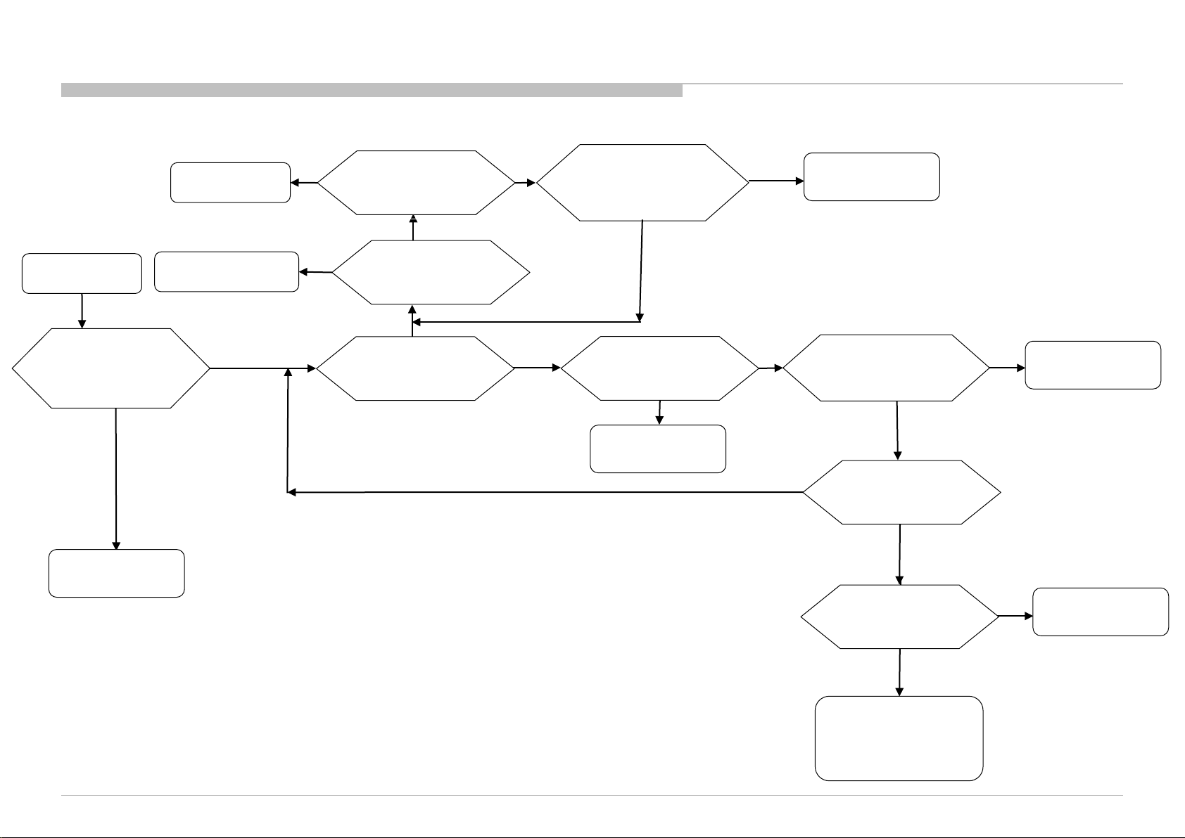
3-2. NO POWER
3-2-7. : No Power- IC6014 (5V DDCON) Checking Procedure
Replace F6002 &
Check IC6014
PIN7-PIN9(BBA/BBE)
18V-22.5V?
Yes
Check JL6018.
18V-22.5V?
Start
F6002 damage
Refer Protection Circuit
Checking Procedure
Yes
No
No
Replace IC6014 &
Check IC6014
PIN7-PIN9 (BBA/BBE)
18V-22.5V?
No
Yes
IC6014 damage.
Check voltage at
JL6019(BBA/BBE).
5.00V-5.19V?
Yes
Refer IC6010
Checking
Procedure
No
No
Check IC6014
PIN7-PIN9(BBA/BBE)
18V-22.5V?
Yes
Check CL6054(BBA/BBE)
3.89V-4.71V?
No
Check R6228 &
R6229 mounting
condition.
Yes
OK
Replace IC6014 &
check again JL6019.
5.00V-5.19V?
No
Check JL6019 by
Continuity Test.
OK or short?
Short
Check & remove any
foreign material
attach to the board.
Still shorted?
Short
Refer to IC6010, USB &
H-Board
Checking Procedure
Yes
No
IC6014 damage.
Foreign material
38
Page 39
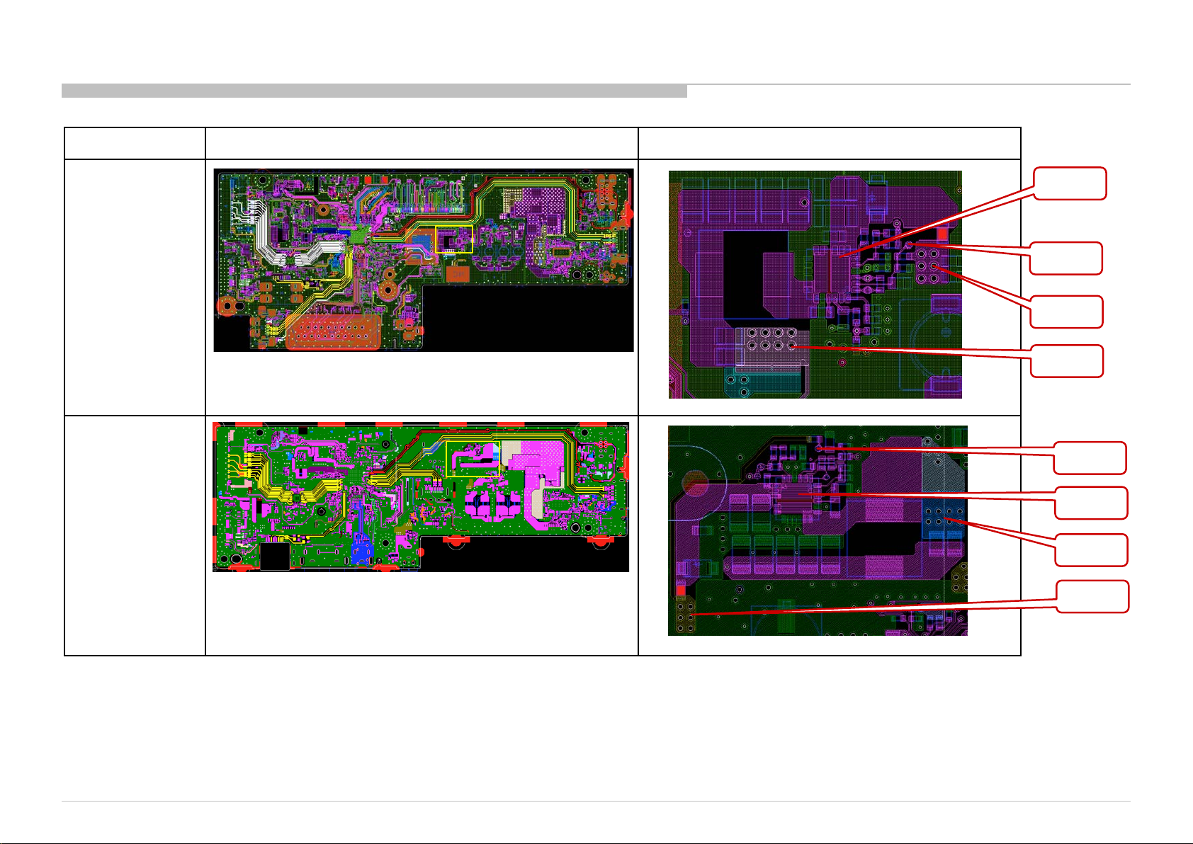
IC6014 Checking Procedure- Checking Point
Board Name Board PWB (A side) Detail
BBE
(5V)
BBA
(5V)
IC6014
CL6054
JL6018
JL6019
CL6054
IC6014
JL6019
JL6018
39
Page 40
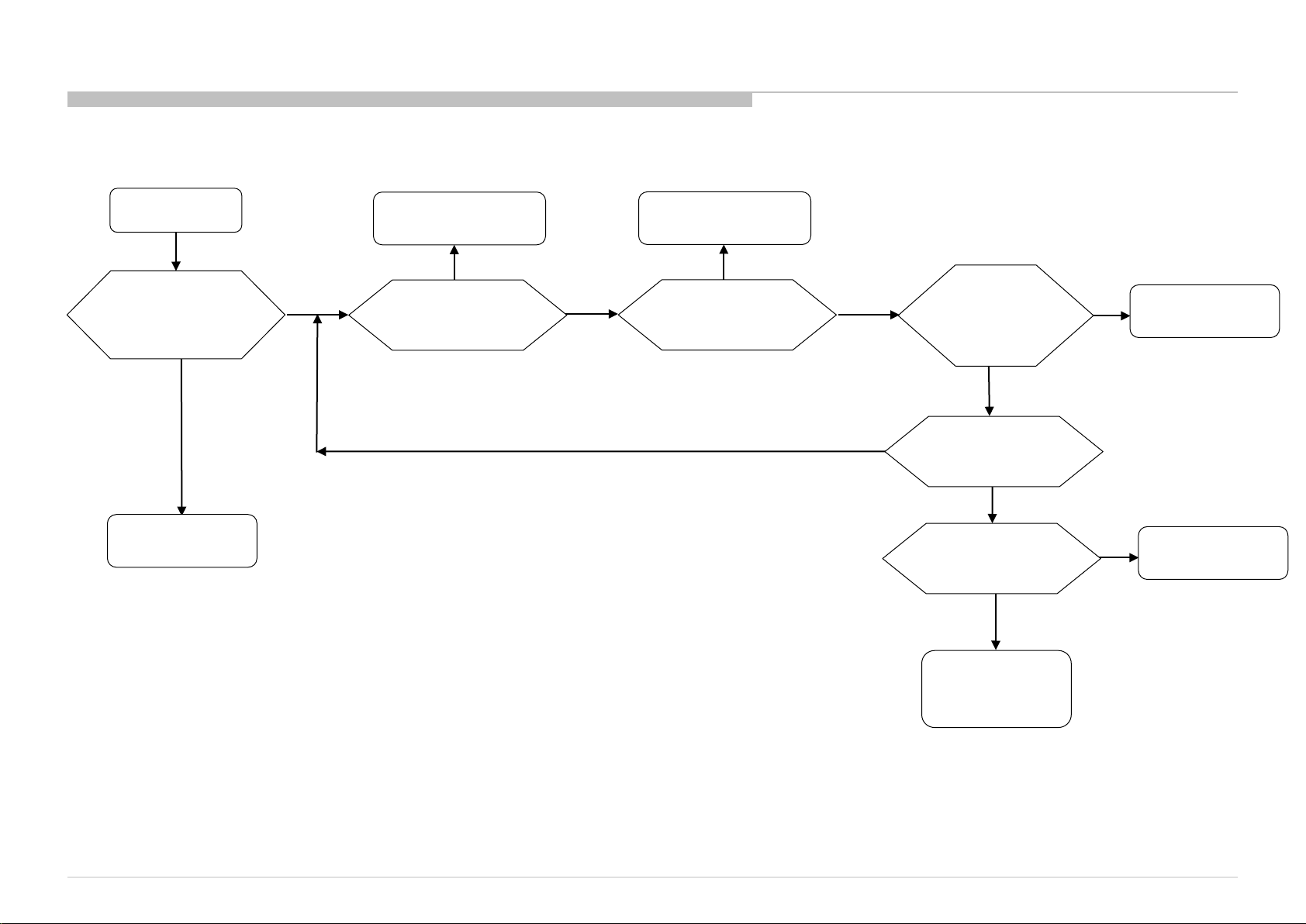
3-2-8. No Power-IC6010 (3.3V_STBY DDCON) Checking Procedure
Start
Check voltage at
JL6036(BBA/BBE).
3.267V-3.333V?
Yes
Refer IC6017
Checking
Procedure
No
Refer IC6014
Checking Procedure
No
Check CL6035(BBA/BBE)
5.00V-5.19V?
Yes
Refer IC6014
Checking Procedure
No
Check CL6035(BBA/BBE)
5.00V-5.19V?
Yes
OK
Replace
IC6010 & check
again at
JL6036.
3.267V-
3.333V?
No
Check JL6036 by
Continuity Test.
OK or short?
Short
Check & remove any
foreign material
attach to the board.
Still shorted?
Short
Yes
No
IC6010 damage.
Foreign material
MTK damage or
Refer to H-Board
Checking
Procedure
40
Page 41

IC6010 Checking Procedure (Checking Point)
Board Name Board PWB (A side) Detail
BBE
(STBY_3.3V)
BBA
(STBY_3.3V)
IC6010
JL6036
CL6035
CL6035
IC6010
JL6036
41
Page 42
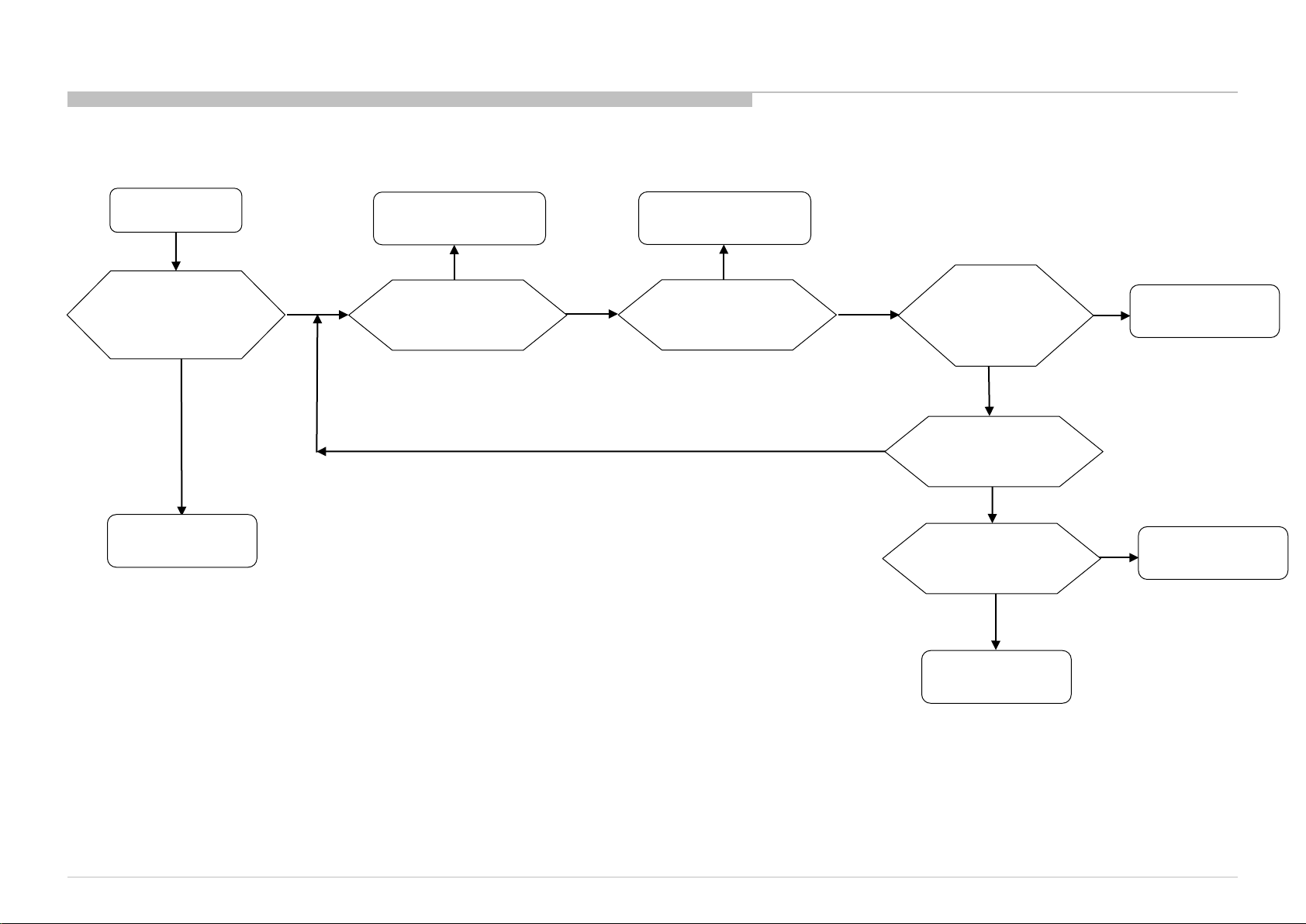
3-2.9. No Power-IC6017(1.2V DDCON) Checking Procedure
Start
Check voltage at
JL6040(BBE)/
JL6031(BBA).
1.18V-1.22V?
Yes
End
No
Refer IC6014
Checking Procedure’
No
Check CL6064(BBA/BBE)
5.00V-5.19V?
Yes
TV in stand-by mode.
No
Check JL6027(BBA/BBE)
3.00V-3.33V?
Yes
OK
Replace
IC6017 & check
again
JL6040(BBE)/
JL6031(BBA).
1.18V-1.22V?
No
Check JL6040(BBE)/
JL6031(BBA).
by Continuity Test.
OK or short?
Short
Check & remove any
foreign material
attach to the board.
Still shorted?
Short
Yes
No
IC6017 damage.
Foreign material
MTK damage.
42
Page 43
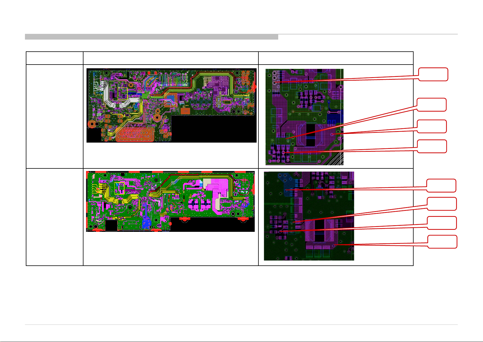
IC6017 Checking Procedure (Checking Point)
Board Name Board PWB (A side) Detail
BBE
(1.2V)
BBA
(1.2V)
CL6064
IC6017
JL6040
CL6065
CL6064
IC6017
CL6065
JL6031
43
Page 44
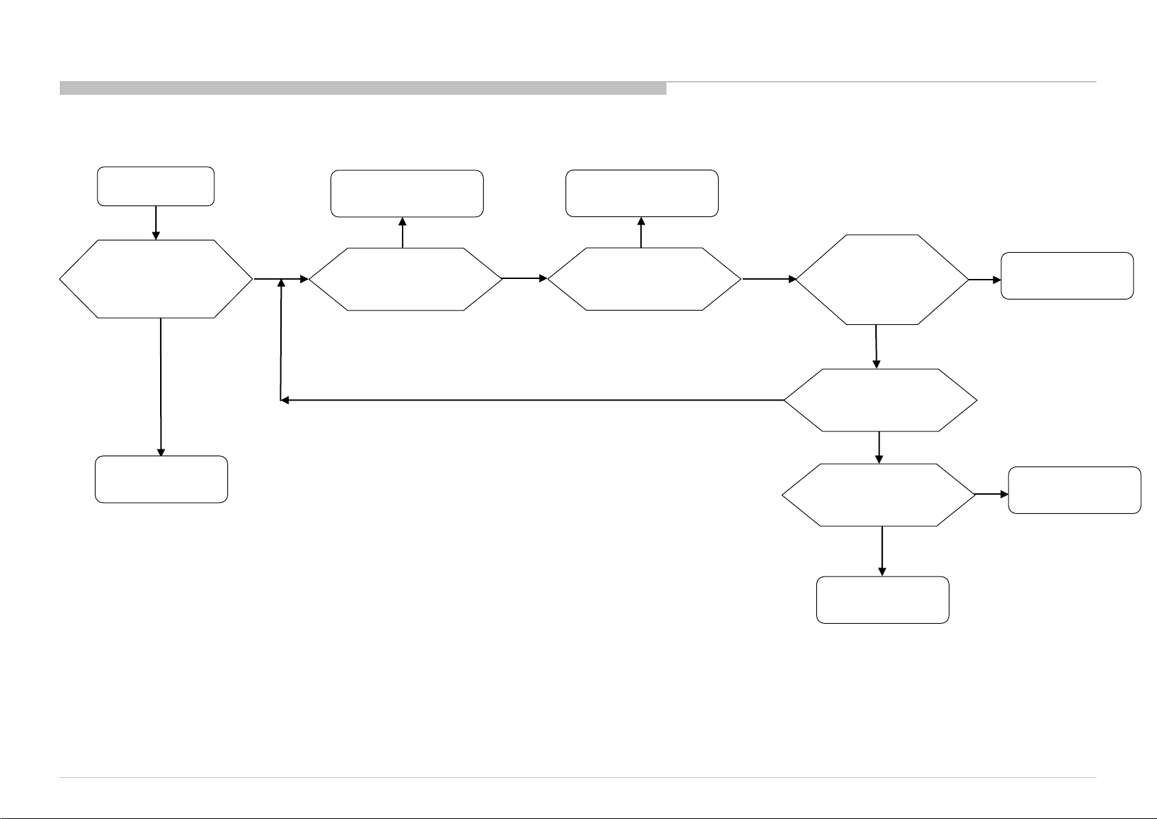
3-2-11. No Power-IC6012(1.5V DDCON) Checking Procedure
Start
Check voltage at
JL6037(BBE)/
JL6033(BBA).
1.48V-1.54V?
Yes
End
No
Refer IC6014
Checking Procedure’
No
Check CL6039(BBA/BBE)
5.00V-5.19V?
Yes
TV in stand-by mode
or MTK damage.
No
Check CL6043(BBA/BBE)
3.00V-3.33V?
Yes
OK
Replace
IC6012 & check
again
JL6037(BBE)/
JL6033(BBA).
1.48V-1.54V?
No
Check JL6037(BBE)/
JL6033(BBA).
by Continuity Test.
OK or short?
Short
Check & remove any
foreign material
attach to the board.
Still shorted?
Short
Yes
No
IC6012 damage.
Foreign material
MTK damage.
44
Page 45
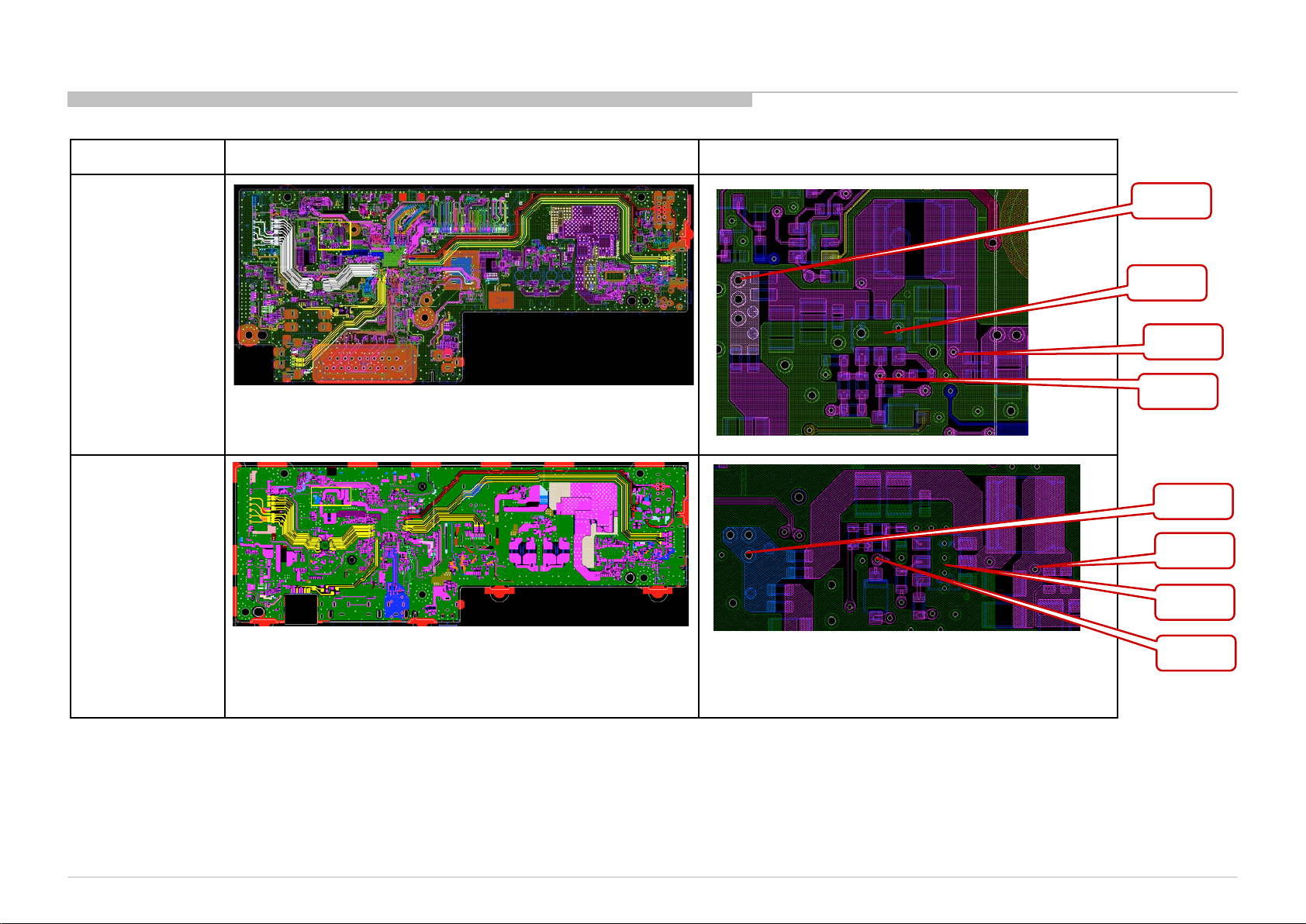
IC6012 Checking Procedure (Checking Point)
Board Name Board PWB (A side) Detail
BBE
(1.5V)
BBA
(1.5V)
CL6039
IC6012
JL6037
CL6043
CL6039
JL6033
IC6012
CL6043
45
Page 46
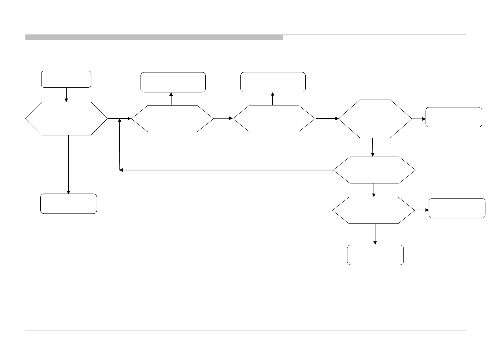
3-2-12. No Power-IC6018(1.8V DDCON) Checking Procedure
Start
Check voltage at
JL6039(BBE)/
JL6032(BBA).
1.78V-1.86V?
Yes
End
No
Refer IC6014
Checking Procedure’
No
Check CL6069(BBA/BBE)
5.00V-5.19V?
Yes
TV in stand-by mode.
No
Check CL6070(BBA/BBE)
3.00V-3.33V?
Yes
OK
Replace
IC6018 & check
again
JL6039(BBE)/
JL6032(BBA).
1.78V-1.86V?
No
Check JL6039(BBE)/
JL6032(BBA).
by Continuity Test.
OK or short?
Short
Check & remove any
foreign material
attach to the board.
Still shorted?
Short
Yes
No
IC6018 damage.
Foreign material
Refer Tuner
Checking
Procedure
46
Page 47

IC6018 Checking Procedure (Checking Point)
Board Name Board PWB (A side) Detail
BBE
(3.3V)
BBA
(3.3V)
CL6012
CL6037
IC6009
JL6038
CL6037
IC6009
JL6034
CL6012
47
Page 48
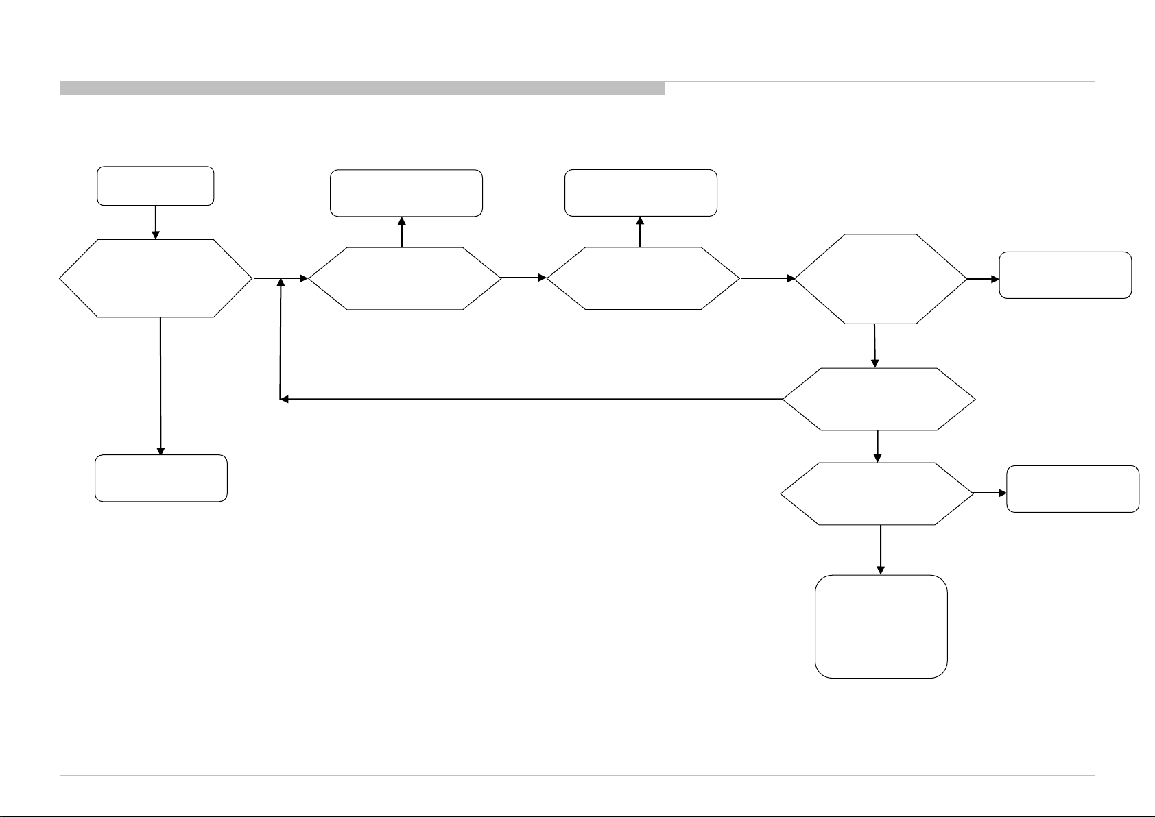
3-2-13. No Power-IC6009( 3.3V DDCON) Checking Procedure
Start
Check voltage at
JL6038(BBE)/
JL6034(BBA).
3.267V-3.333V?
Yes
End
No
Refer IC6014
Checking Procedure’
No
Check CL6037(BBA/BBE)
5.00V-5.19V?
Yes
TV in stand-by
mode.
No
Check CL6012(BBA/BBE)
3.00V-3.33V?
Yes
OK
Replace IC6009
& check again
at
JL6038(BBE)/
JL6034(BBA).
3.267V-3.333V?
No
Check JL6038(BBE)/
JL6034(BBA) by
Continuity Test.
OK or short?
Short
Check & remove any
foreign material
attach to the board.
Still shorted?
Short
Yes
No
IC6009 damage.
Foreign material
Refer LED Driver,
Nand, USB, Audio,
H-Board, Tuner,
MTK Checking
Procedure
48
Page 49
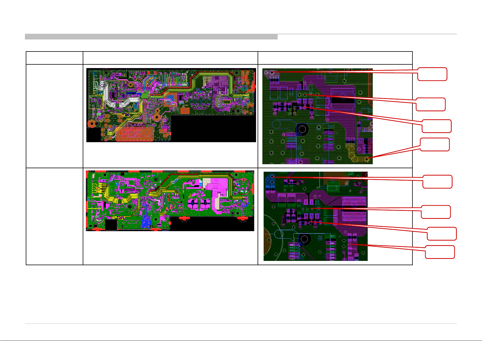
IC6009 Checking Procedure (Checking Point)
Board Name Board PWB (A side) Detail
BBE
(1.8V)
BBA
(1.8V)
CL6069
IC6018
CL6070
JL6039
CL6069
IC6018
CL6070
JL6032
49
Page 50
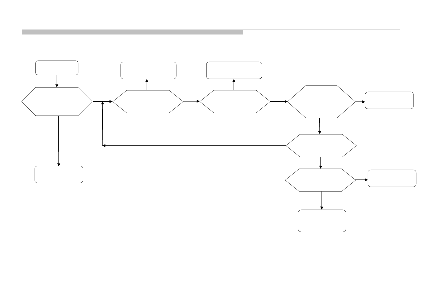
3-2-14. No Power-IC6016(1.1V DDCON) Checking Procedure
Start
Check voltage at
JL6035(BBA/BBE).
1.09V-1.11V?
Yes
End
No
Refer IC6010
Checking Procedure’
No
Check CL6037(BBA/BBE)
3.267V-3.333V?
Yes
TV in stand-by mode
or MTK damage.
No
Check CL6008 (BBA/BBE)
3.00V-3.33V?
Yes
OK
Replace IC6016
& check again at
JL6035
(BBA/BBE).
1.09V-1.11V?
No
Check JL6035
(BBA/BBE) by
Continuity Test.
OK or short?
Short
Check & remove any
foreign material
attach to the board.
Still shorted?
Short
Yes
No
IC6016 damage.
Foreign material
Refer Beryls
Checking
Procedure
50
Page 51
Troubleshooting
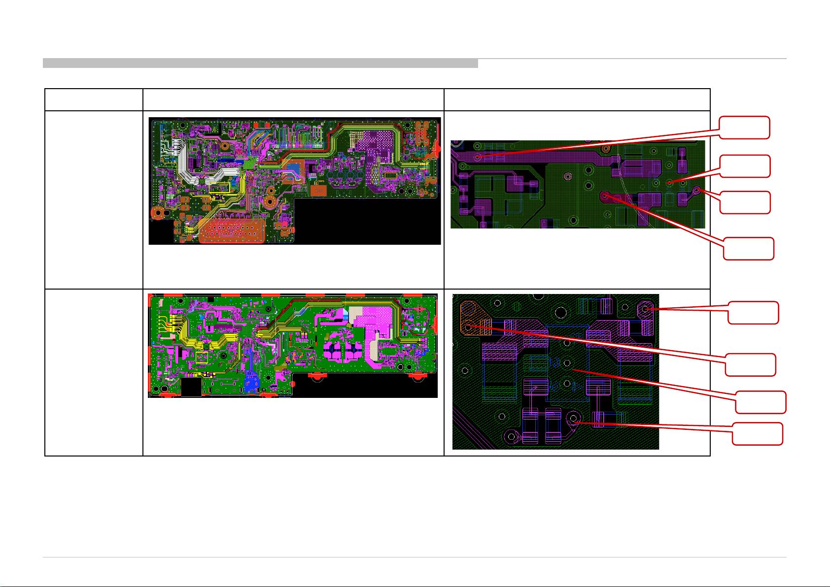
IC6016 Checking Procedure (Checking Point)
Board Name Board PWB (A side) Detail
BBE
(1.1V)
BBA
(1.1V)
JL6035
IC6016
CL6008
CL6062
JL6035
CL6060
IC6016
CL6008
51
Page 52
Troubleshooting
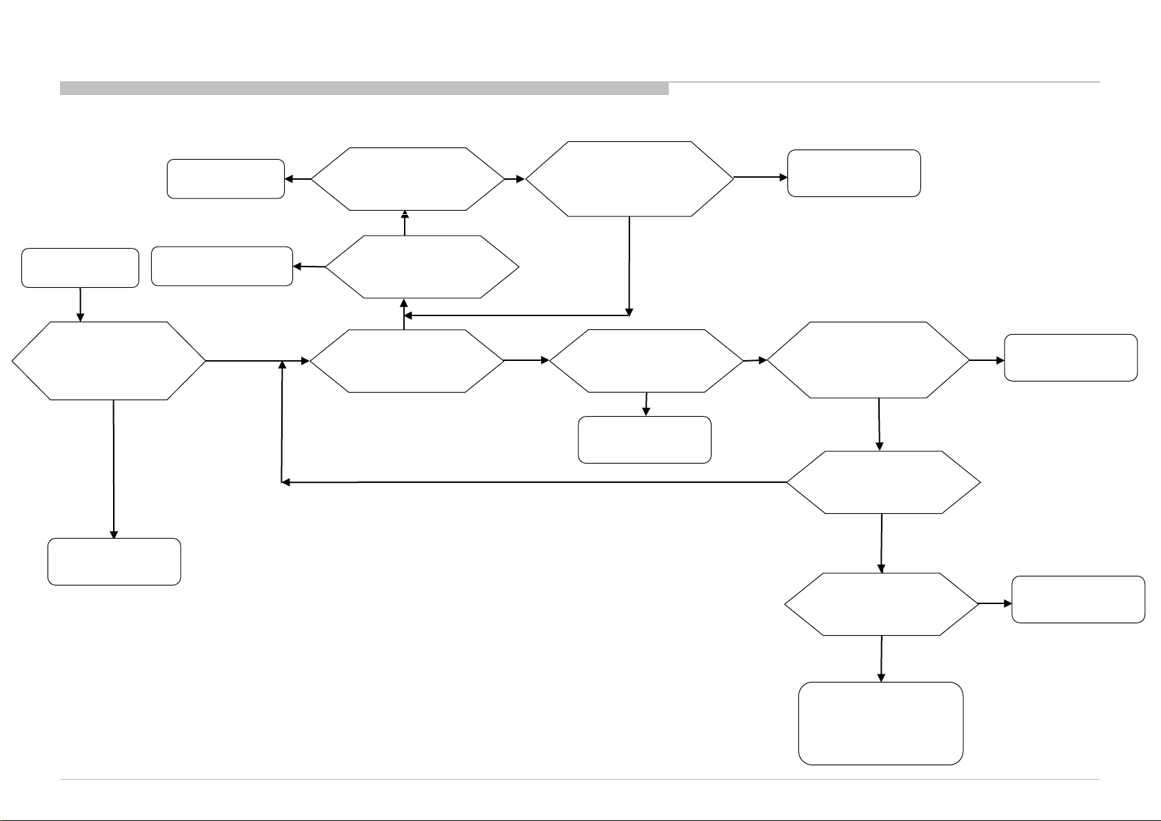
3-2-15. No Power-IC6019(12V DDCON) Checking Procedure
Replace F6003 &
Check IC6019
PIN-2 (BBA/BBE)
18V-22.5V?
Yes
Check JL6018.
18V-22.5V?
Start
F6003 damage
Refer Protection Circuit
Checking Procedure
Yes
No
No
Replace IC6019 &
Check IC6019
PIN-2 (BBA/BBE)
18V-22.5V?
No
Yes
IC6019 damage.
Check voltage at
JL6030(BBA)
JL6034(BBE)
11.52V-12.82V?
Yes
End
No
No
Check IC6019
PIN-2 (BBA/BBE)
18V-22.5V?
Yes
Check IC6019 (PIN-3)
3.00V-3.33V?
No
MTK Problem or
TV in stand-by
mode.
Yes
OK
Replace IC6019 &
check again
JL6030(BBA)
JL6034(BBE)
11.52V-12.82V?
No
Check JL6030(BBA)
JL6034(BBE)
by Continuity Test.
OK or short?
Short
Check & remove any
foreign material
attach to the board.
Still shorted?
Short
Refer to LVDS Checking
Procedure
Yes
No
IC6014 damage.
Foreign material
52
Page 53
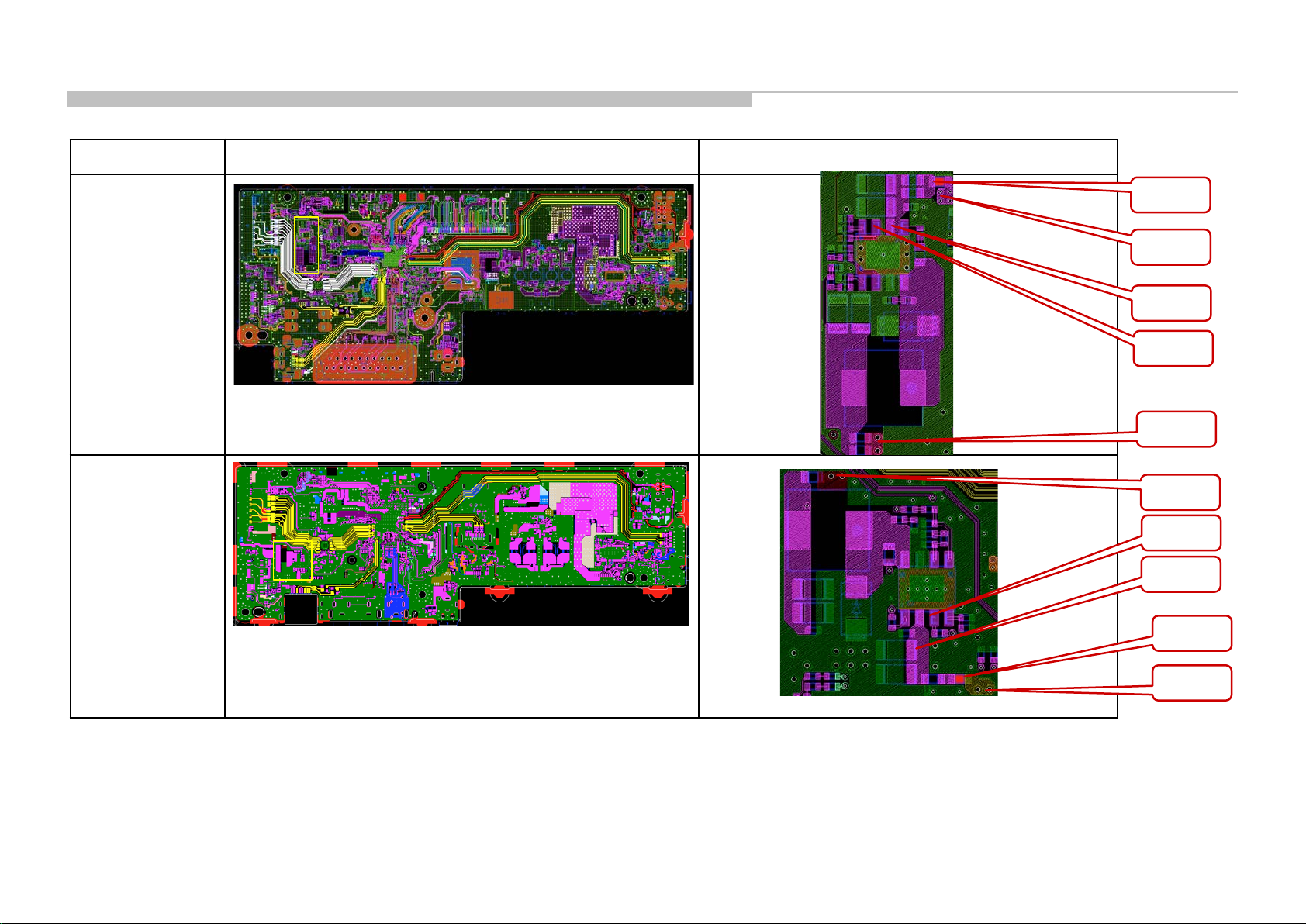
Troubleshooting
No Power-IC6019 Checking Procedure (Checking Point)
Board Name Board PWB (A side) Detail
BBE
(12V)
BBA
(12V)
F6003
JL6018
PIN-2
PIN-3
JL6034
JL6030
PIN-3
PIN-2
F6003
JL6018
53
Page 54
3-3. No Picture
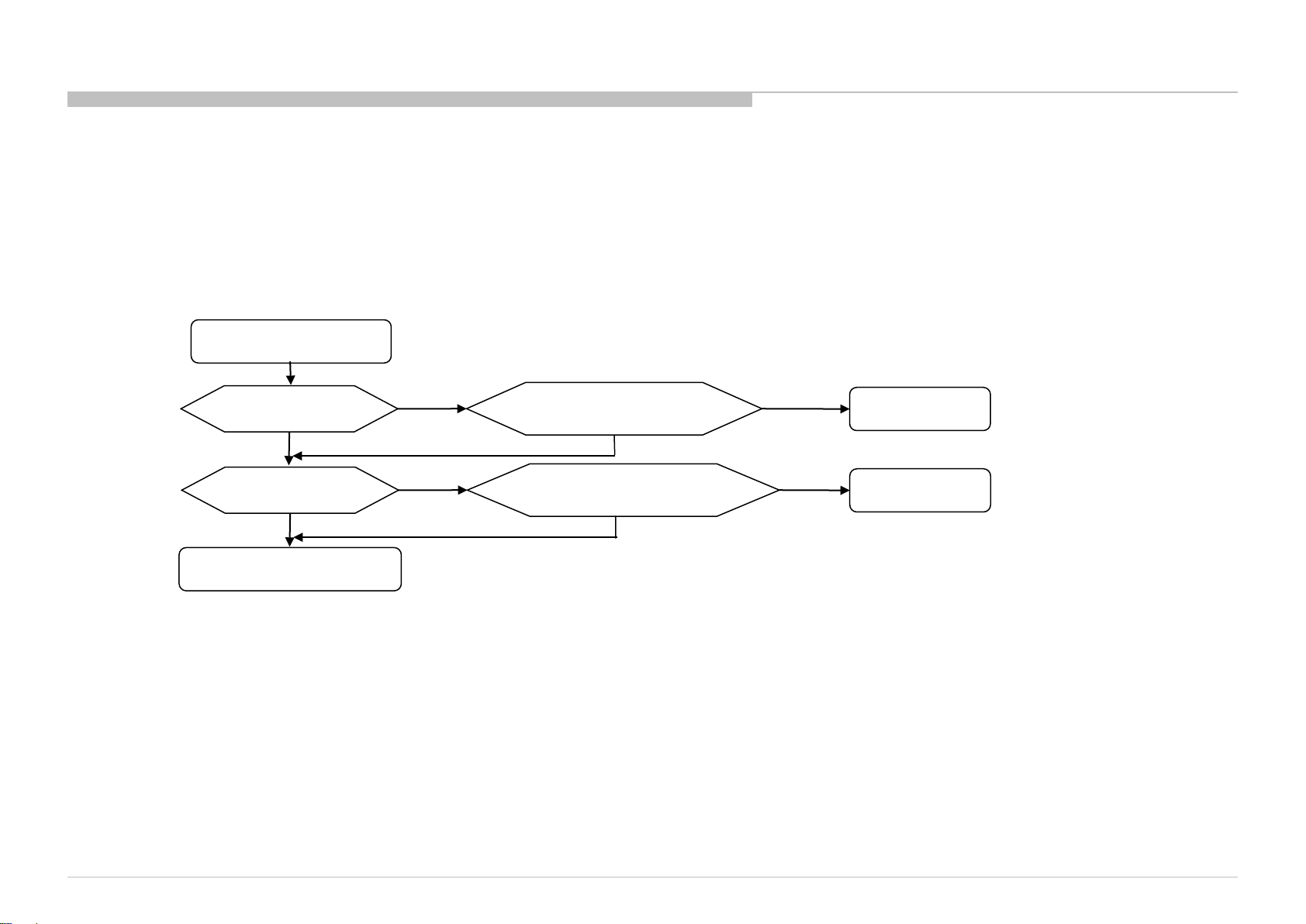
3-3-1. Screen Blank, No Backlight [For QW/QT]
Screen Blank, No backlight
Check R9021
R >9Ω and <11Ω?
Yes
Check REG9V (AC ON)
V=8.9V to 9.1V?
Yes
Suspect : Other Part damage
Change the board
No
Yes
No
Yes
Change R9021
AC ON screen blank, No backlight?
Change IC9000
AC ON screen blank, No backlight?
No
R9021 broken
No
IC9000 broken
54
Page 55
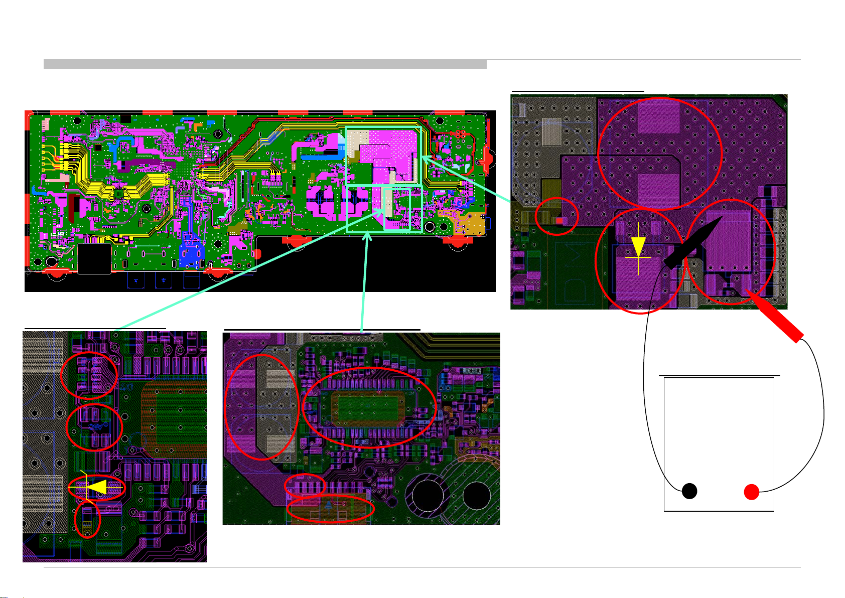
Screen Blank, No Backlight - Checking Point [1/2]-BBA
F9000, L9001, D9001, Q9000
L9001
F9000
S
Q9000
D9001
D
RB9001, Q9001, D9002, R9021
RB9001
Q9001
D9002
R9021
C9026, C9027, CN9000, IC9000, LED_VCC
C9026
IC9000
C9027
LED_VCC
CN9000
Q9000 RDS Measurement
Multimeter
-ve
+ve
55
Page 56

Screen Blank, No Backlight - Checking Point [2/2]-BBE
F9000, L9001, D9001, Q9000
L9001
F9000
S
Q9000
D9001
D
RB9001, Q9001, D9002, R9021
RB9001
Q9001
D9002
R9021
C9026, C9027, CN9000, IC9000, LED_VCC
C9026
IC9000
C9027
LED_VCC
CN9000
Q9000 RDS Measurement
Multimeter
-ve
+ve
56
Page 57
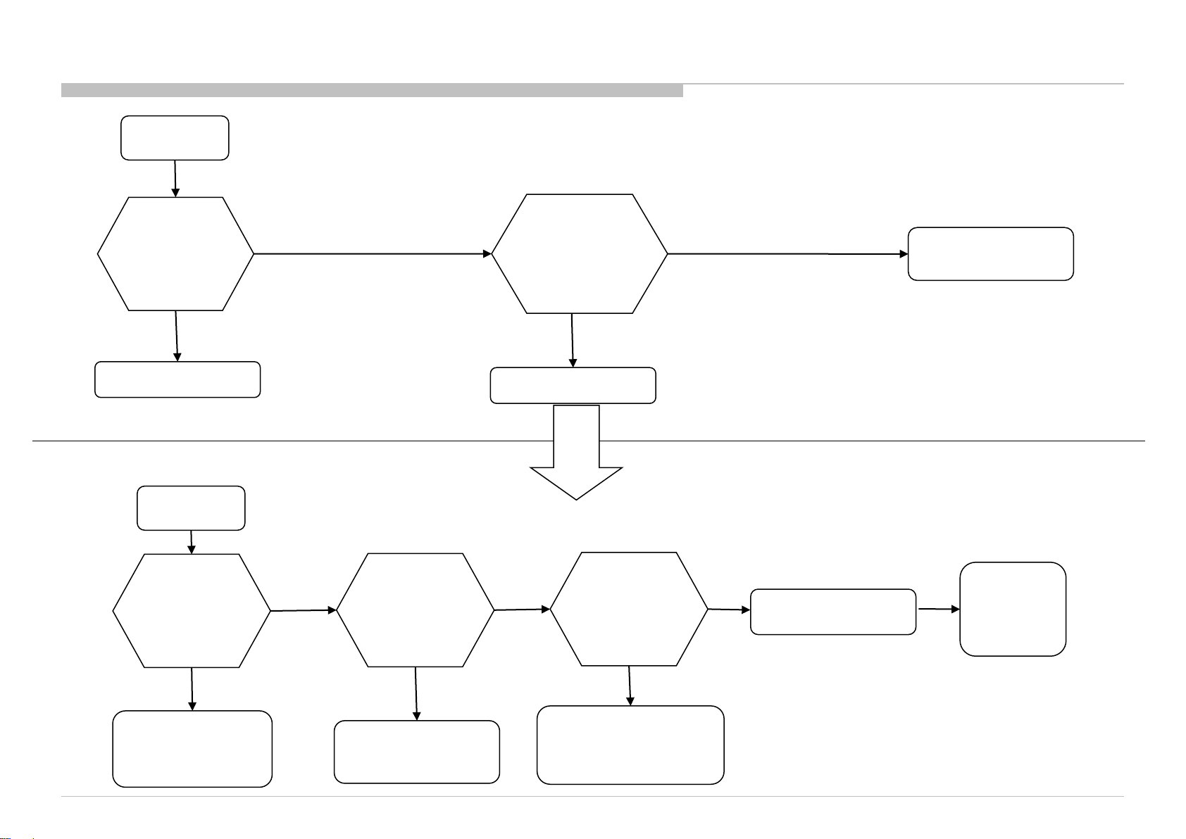
3-3-2. Screen Blank, Backlight visible(General Checking)
START
Replace LVDS FFC
Harness
Picture OK
LVDS FFC Harness Problem
Still No Picture
Troubleshooting Detail No Picture (Main Board Issue)
START
Still No
Check
1.1 V Supply Voltage
Is it 1.1V?
Picture
Check 3.3V_PANEL
Voltage
Is it 3V- 3.33V?
Change Main Board
Main board problem
Still No
Picture
Check BE_RST Voltage
Picture OK
Is 3V-3.33V ?
Still no picture
Have
Voltage
Suspect IC5001 NG
Change IC5001
Panel Problem
END
Picture OK
No Voltage
Refer to 1.1V DDCON
Troubleshooting manual
(IC 6016)
No Voltage
Refer to Panel I2C
Checking Manual
No Voltage
Suspect IC5000 NG
Replace Board
57
Page 58
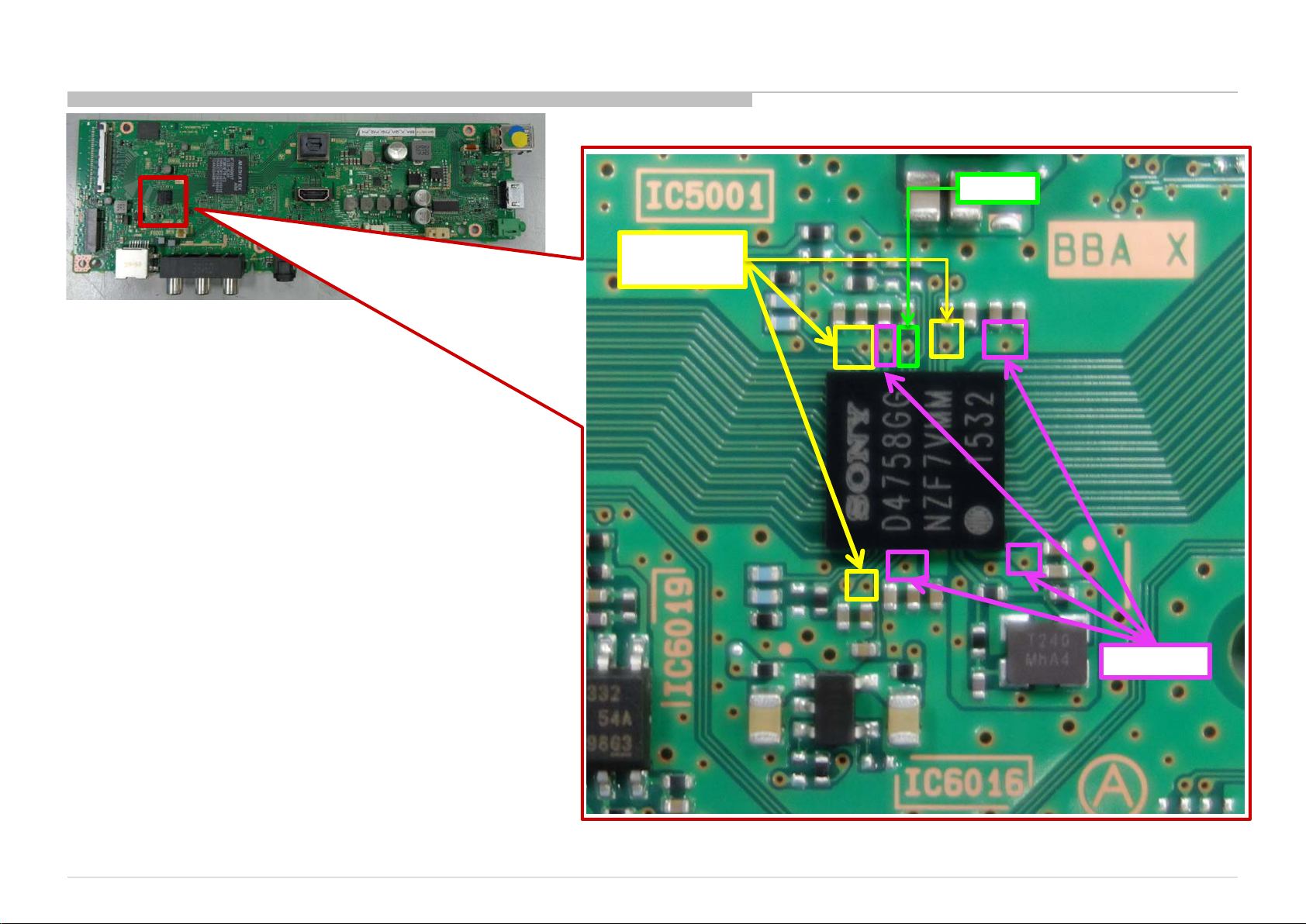
Screen Blank, Backlight visible(Checking Point )-BBA
Check Item:
1. Supply voltage
2. Supply voltage impedance
BE_RST
3.3V_PANEL
Supply
1.1V Supply
58
Page 59
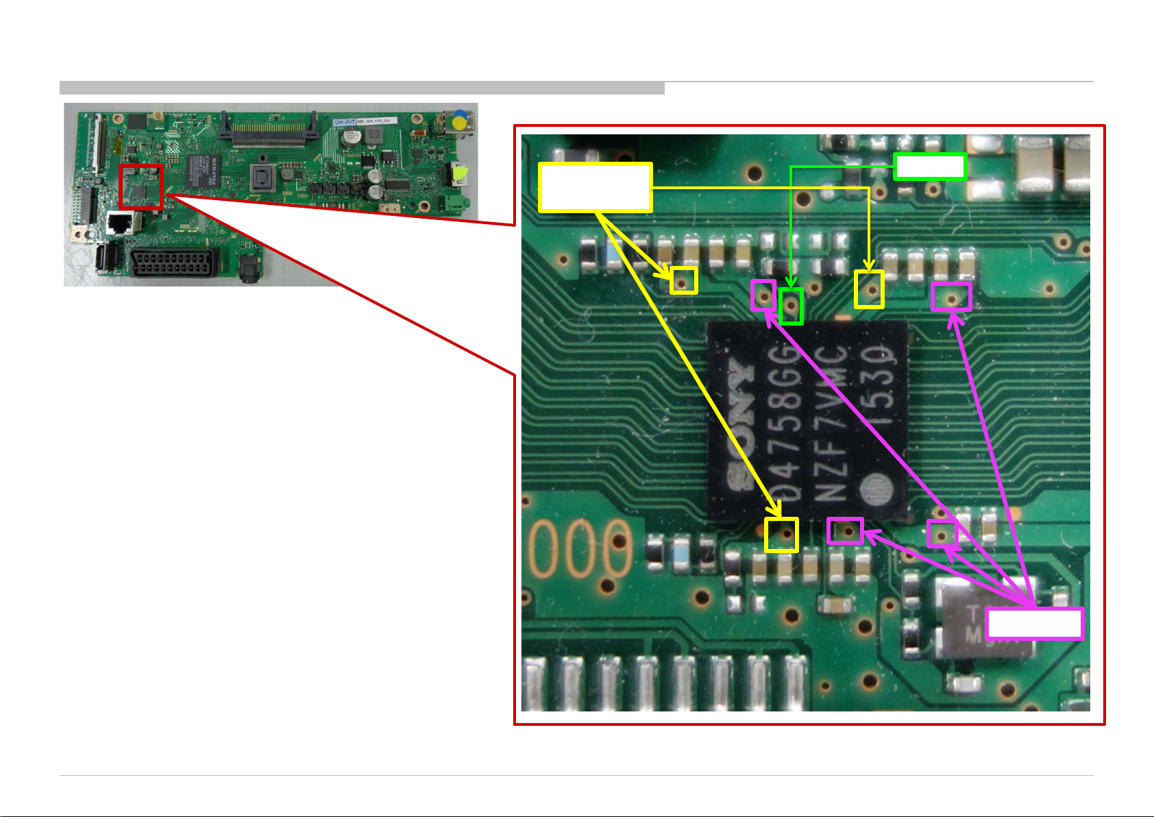
Screen Blank, Backlight visible(Checking Point )-BBE
Check Item:
1. Supply voltage
2. Supply voltage impedance
3.3V_PANEL
Supply
BE_RST
1.1V Supply
59
Page 60
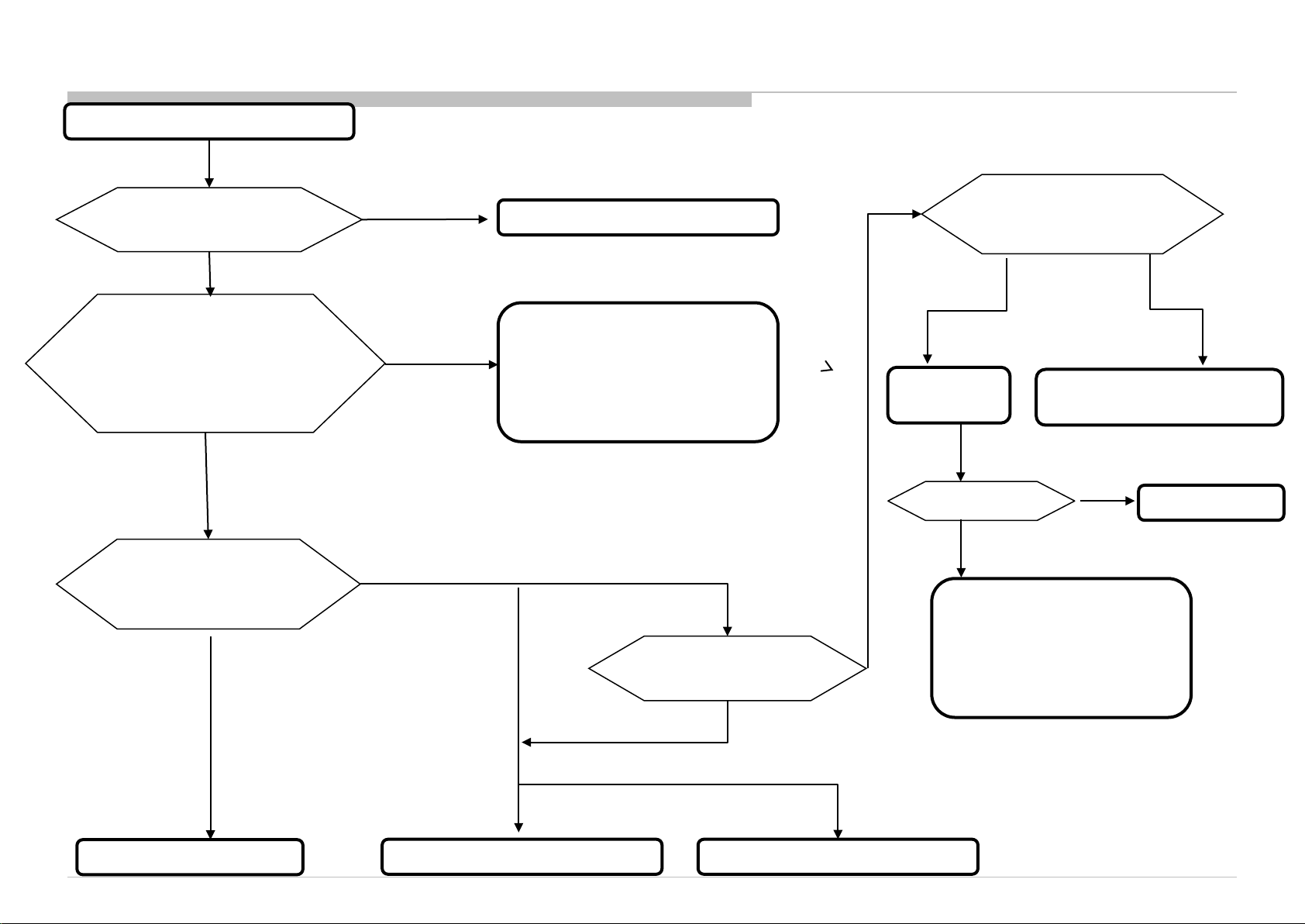
3.3.3 : No Picture: Tuner (for Analogue , Digital and Satellite)
RF input no picture / noisy picture
Check RF source cable
and antenna, OK?
OK
Check Tuner power line:
3.3V at CL1005 = 3.3V?
1.8V at C1019 = 1.8V?
OK
Tuning for Analog, Digital or
Satellite?
NG
NG
Digital
Change RF cable and antenna
For 1.8V Please refer DDCON
troubleshooting
For 3.3V Please refer DDCON
troubleshooting
Check Tuner power line
12V at F1000 = 12V?
Satellite
Change part
Problem solved?
NG
Check fuse F1000 continuity.
Part broken?
YES
Please refer DDCON 12V LNB
F1000
NG
Change Tuner Module EU-
(Please refer page Assemble
and Dissemble Tuner Module)
Voltage troubleshooting
OK
T2S2
(CE243ZP )
NO
Done (End)
Refer Analog Tuning
For TW , LA-ATSC
(MX/UC) , LA-ISDB(BR) ,
PH_ISDB-T & AEP (STD)
only
Refer Digital Tuning 1
OK
For AEP-T2S2, PA_T2,
CH and LA-T2(COL) only
Refer Digital Tuning 2
60
Page 61
No Picture : Tuner (for Analogue , Digital and Satellite)-Checking Point
Board Name Board PWB (B side) Detail
BBA board
(A side)
(3.3V)
C1005
(1.8V)
C1019
BBE board
(A side)
(3.3V)
C1005
(1.8V)
C1019
BBA board
(A side)
Detail
BBE board
(A side)
C1019
C1005
F1000
C1019
Detail
C1005
61
Page 62
3.3.4 : For Analogue Tuning Failed ( All destination)
Analog Tuning
For Other destination
Channel can be lock?
OK
For LA-ISDB(BR/AR),
PH_ISDB-T &
LA-T2(COL)
NG
Notes:
- Parts for IFOUTN1 line: FB1000, C1011, C1027, R1055, R1057
- Parts for IFOUTP1 line: FB1001, C1012, C1028, R1056
- Parts for IFAGC1 line: C1029, R1058
Confirm Antenna or Cable connection
Picture quality is noisy?
Not Noisy
Done (End)
Noisy
OK
Check part mounting condition
for analog control line
“IFOUTN1, IFOUTP1, IFAGC1”
OK
Please re-upgrade Firmware
(PKG), Check again Picture
quality?
NG
NG
Change Tuner Module
(Please refer page Assemble and Dissemble Tuner Module)
OK
Problem solved?
NG
Change B-board
62
Page 63
For Analogue Tuning Failed -Checking Point [1/4]
Board Name Board PWB (A side) Detail
BBA board
(A side)
(IFOUTN1)
FB1000
C1011
C1027
R1055
(IFOUTP1)
FB1001
C1012
C1028
R1056
C1027
C1027
C1027
FB1001
C1056
C1028
C1011
C1012
FB1000
C1011
63
Page 64
For Analogue Tuning Failed -Checking Point [2/4]
Board Name Board PWB (A side) Detail
BBA board
(A side)
(IFAGC1)
C1029
R1058
R1058
C1029
64
Page 65
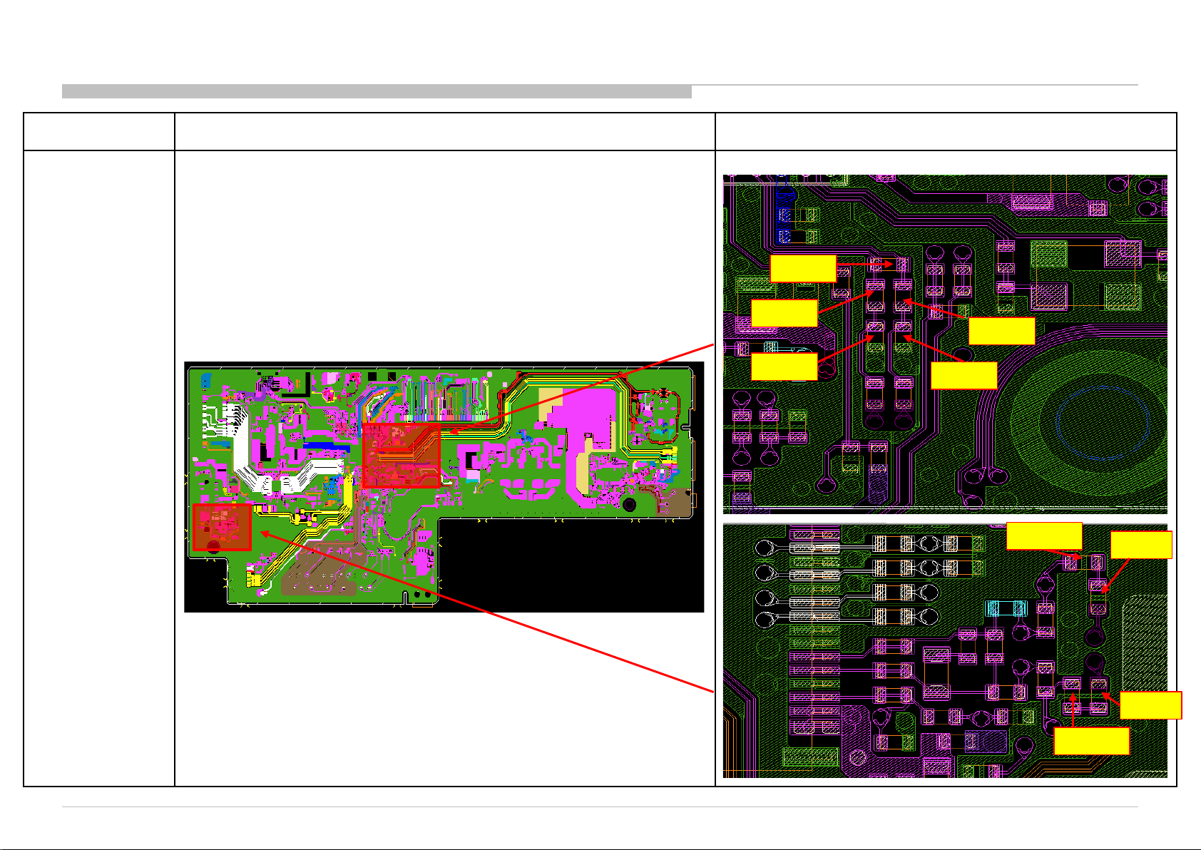
For Analogue Tuning Failed - Checking Point [3/4]
Board Name Board PWB (A side) Detail
BBE board
(A side)
(IFOUTN1)
FB1000
C1011
C1027
R1055
(IFOUTP1)
FB1001
C1012
C1028
R1056
R1057
R1055
C1027
C1028
R1056
FB1001
C1012
FB1000
C1011
65
Page 66
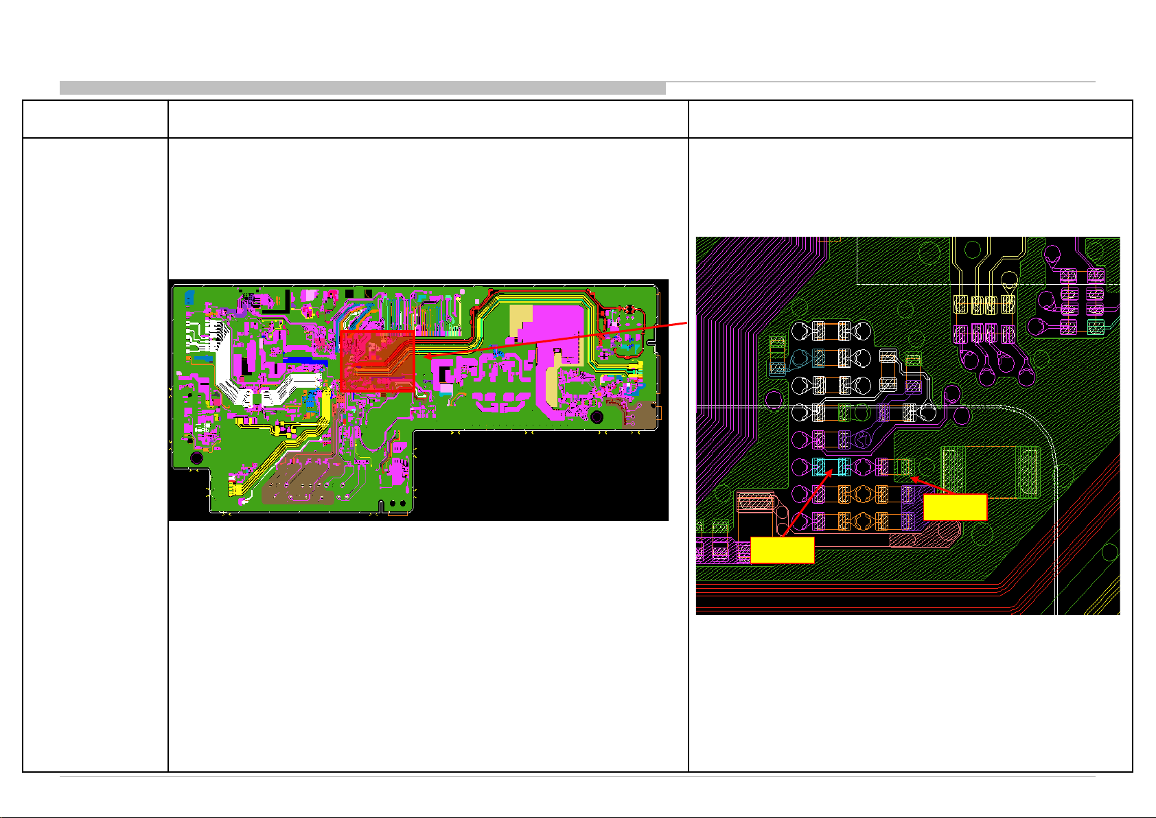
For Analogue Tuning Fail ed -Checking Point [4/4]
Board Name Board PWB (A side) Detail
BBE board
(A side)
(IFAGC1)
C1029
R1058
R1058
C1029
66
Page 67
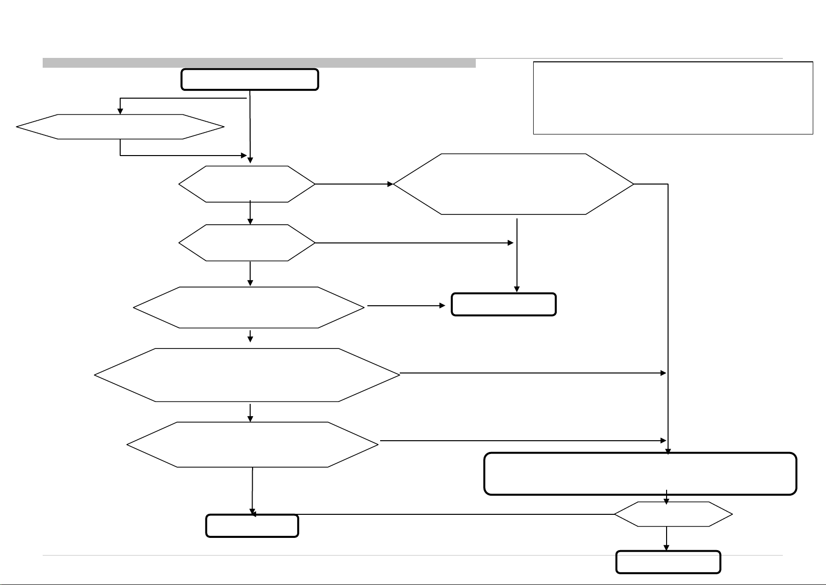
3-3-5. For Digital Tuning 1: Only for TW , AM-ATSC(MX/UC) , LA-ISDB(BR/AR) , PH_ISDB-T , AEP(STD) .
LA-ISDB(BR/AR)
Confirm Antenna or Cable connection
Confirm UEC of digital RF by Service mode
If UEC > 0
Digital Tuning 1
Channel can be lock?
NG
Sound is normal?
No sound
For Other
destination
OK
OK
If UEC = 0
Notes:
- Parts for IFOUTN1 line: FB1000, C1011, C1027, 1055, R1057
- Parts for IFOUTP1 line: FB1001, C1012, C1028, R1056
- Parts for IFAGC1 line: C1029, R1058
- Parts for M_SCL line: R5024
- Parts for M_SDA line: R5021
Check part mounting condition for
digital control line
“M_SCL,M_SDA”
OK
Change B-board
NG
Check part mounting condition for digital data line
“IFOUTN1, IFOUTP1, IFAGC1”
OK
Please re-upgrade Firmware
(PKG),
Check again Picture quality?
OK
Done (End)
NG
NG
Change Tuner Module
(Please refer page Assemble and Dissemble Tuner Module)
OK
Problem solved?
NG
Change B-board
67
Page 68
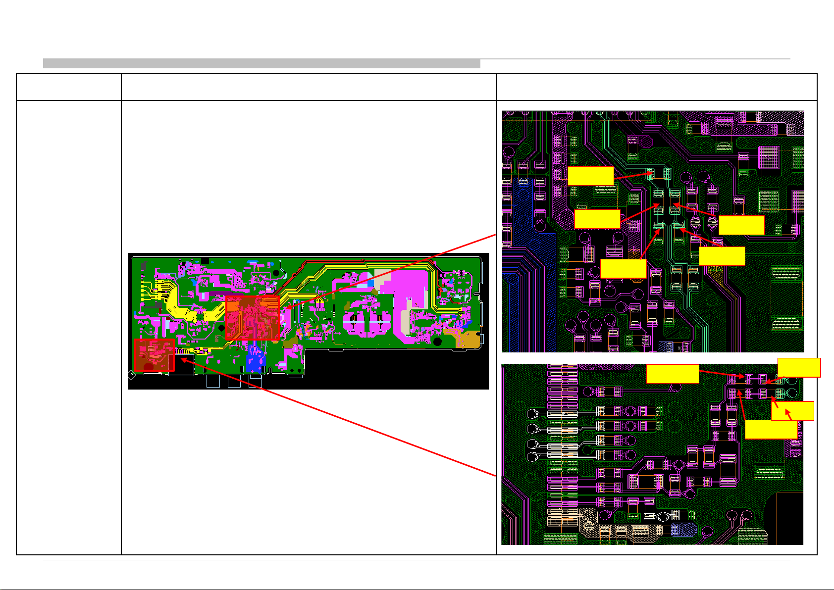
For Digital Tuning 1: Only for TW , AM-ATSC(MX/UC) , LA-ISDB(BR/AR) , PH_ISDB-T , AEP(STD)- Checking Point [1/2]
Board Name Board PWB (A side) Detail
BBA board
(A side)
(IFOUTN1)
FB1000
C1011
C1027
C1027
R1055
C1027
(IFOUTP1)
FB1001
C1012
C1028
C1027
R1056
FB1001
C1056
C1028
C1011
C1012
C1011
FB1000
68
Page 69
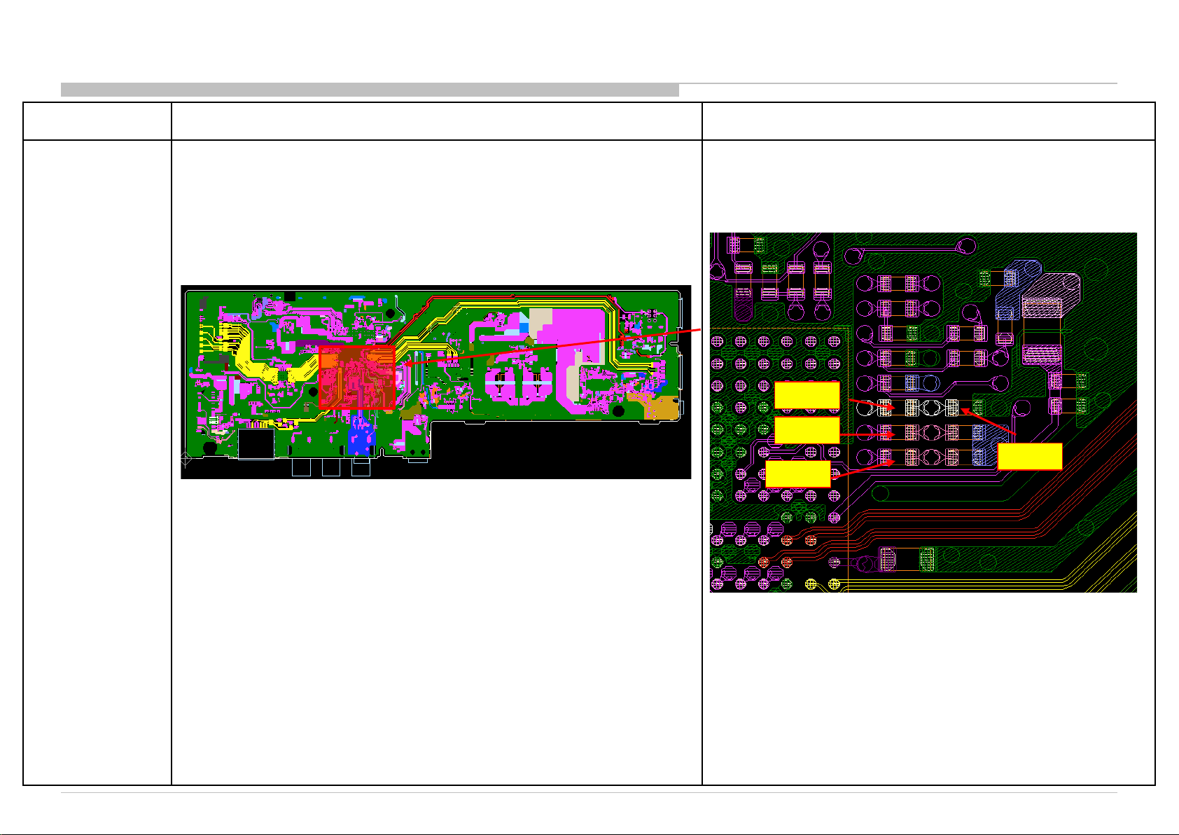
For Digital Tuning 1: Only for TW , AM-ATSC(MX/UC) , LA-ISDB(BR/AR) , PH_ISDB-T , AEP(STD)- Checking Point [ 2/2]
Board Name Board PWB (A side) Detail
BBA board
(A side)
(IFAGC1)
C1029
R1058
(M_SCL)
R5024
(M_SDA)
R5021
R1058
R5024
R5021
C1029
69
Page 70
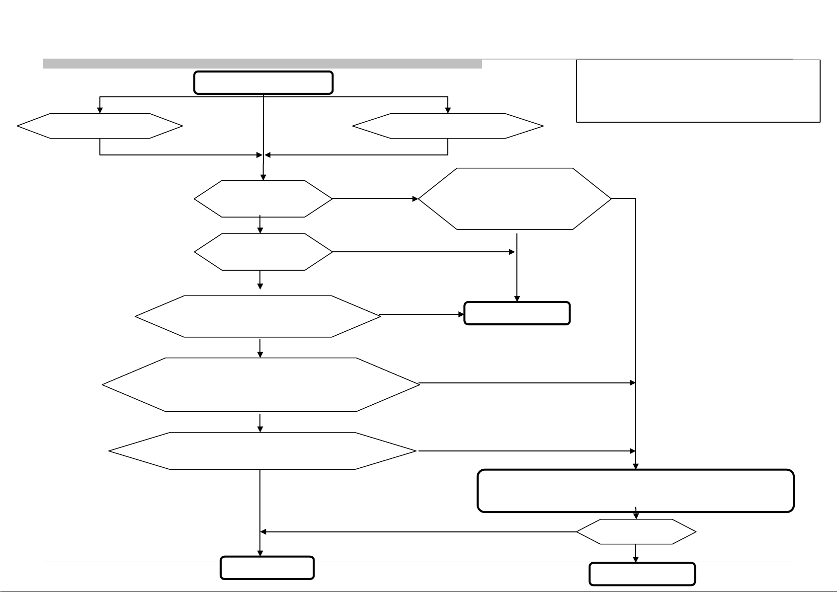
3-3-6. For Digital Tuning 2: AEP-T2S2, EU-T2, PA-T2, CH, and LA-T2(COL).
For and LA-T2(COL) only For AEP-T2S2
Confirm ANT or Cable connection
Digital Tuning 2
For EU-T2,
PA-T2,
and
CH
Confirm ANT or Satellite connection
Notes:
- Parts for M_SCL line: R5024
- Parts for M_SDA line: R5021
- Parts for DEMOD_TSCLK line: R1072
- Parts for DEMOD_TSDATA line: R1071
NG
Channel can be lock?
OK
Sound is normal?
OK
No sound
Confirm UEC of digital RF by Service mode
If UEC > 0
Check part mounting condition for digital data line
“DEMOD_TSCLK, DEMOD_TSDATA”
O
Please re-upgrade Firmware (PKG),
K
Check again Picture quality?
If UEC = 0
NG
NG
Check part mounting condition for
digital control line
“M_SDA,M_SCL”
NG
Change B-board
OK
OK
Done (End)
Change Tuner Module
(Please refer page Assemble and Dissemble Tuner Module)
OK
Problem solved?
NG
Change B-board
70
Page 71
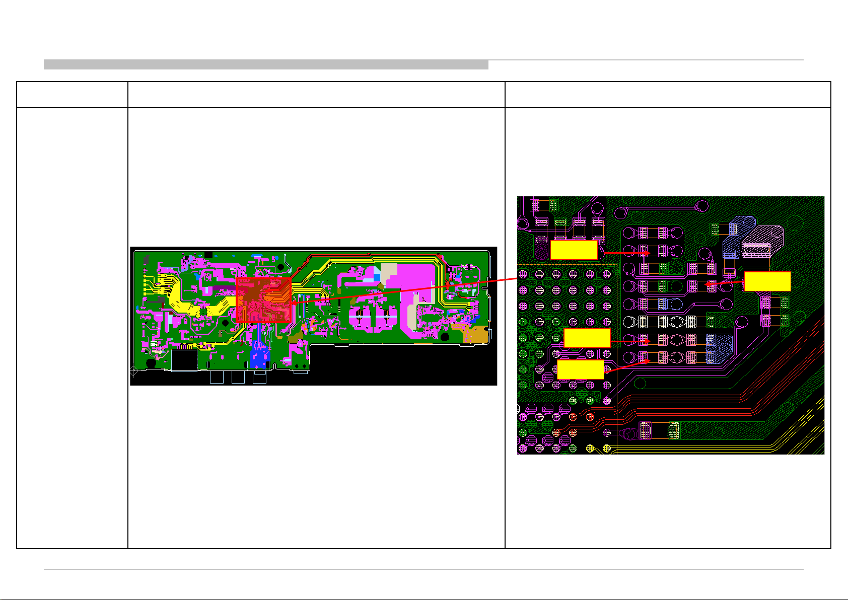
For Digital Tuning 2: AEP-T2S2, EU-T2, PA-T2, CH, and LA-T2(COL)-Checking Point [1/2]
Board Name Board PWB (A side) Detail
BBA board
(A side)
(M_SCL)
R5024
(M_SDA)
R5021
(DEMOD_TSCLK )
R1072
(DEMOD_TSCLK )
R1071
R1072
R1072
R5024
R5021
71
Page 72
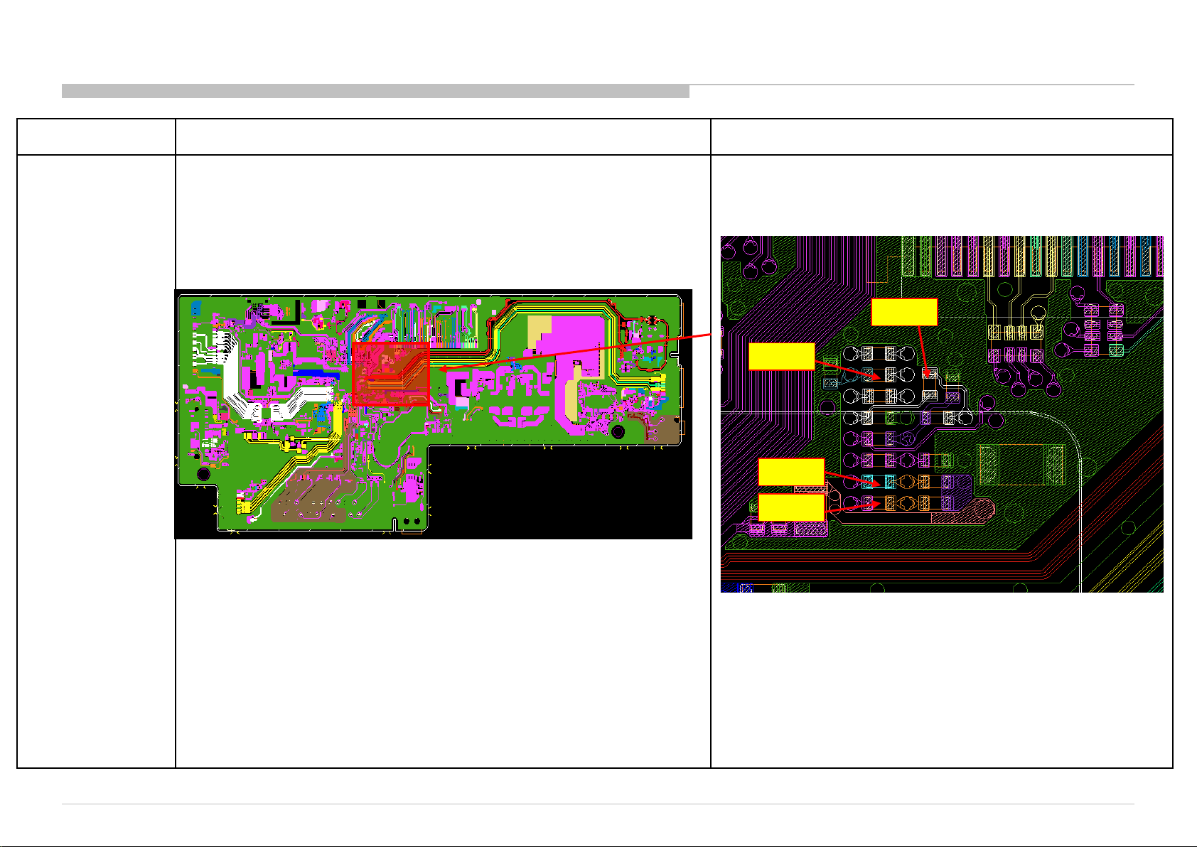
For Digital Tuning 2: AEP-T2S2, EU-T2, PA-T2, CH, and LA-T2(COL)-Checking Point [2/2]
Board Name Board PWB (A side) Detail
BBE board
(A side)
(M_SCL)
R5024
(M_SDA)
R5021
(DEMOD_TSCLK )
R1072
(DEMOD_TSCLK )
R1071
R1072
R1071
R5024
R5021
72
Page 73
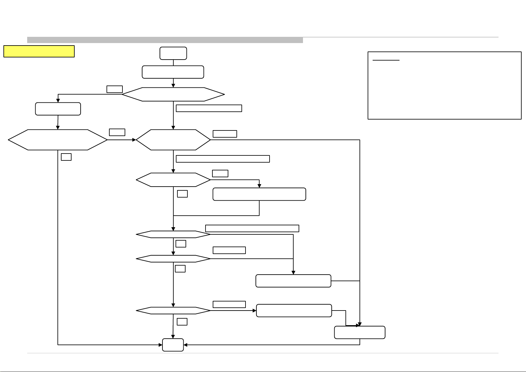
3-3-7. : USB Port1 – No Detection / Cannot Play / No Picture / No Sound
TV turn ON condition:
Change to ON
Detection OK
and
Picture and Sound OK
OK
OFF
NG
START
Do a Factory Setting
*1 Confirm USB Auto
Start is ON or OFF
ON
Check 5V at
C7020 (USB
port1)
Have 5V but No detection
*2 Confirm USB
file format
OK
Detection OK
OK
Picture OK
OK
Remarks:
*1 Confirm USB Auto Start at Set-up Menu.
*2 Confirm with OSD on bottom panel, if
playback not support.
Please refer to IM for detail supported USB
format.
No 5V
NG
Change to supported USB format
USB format OK but No detection
Picture NG
Sound OK
OK
END
Main IC (IC5000) problem
Sound NG
Audio IC IC4001) problem
Change B-Board
73
Page 74
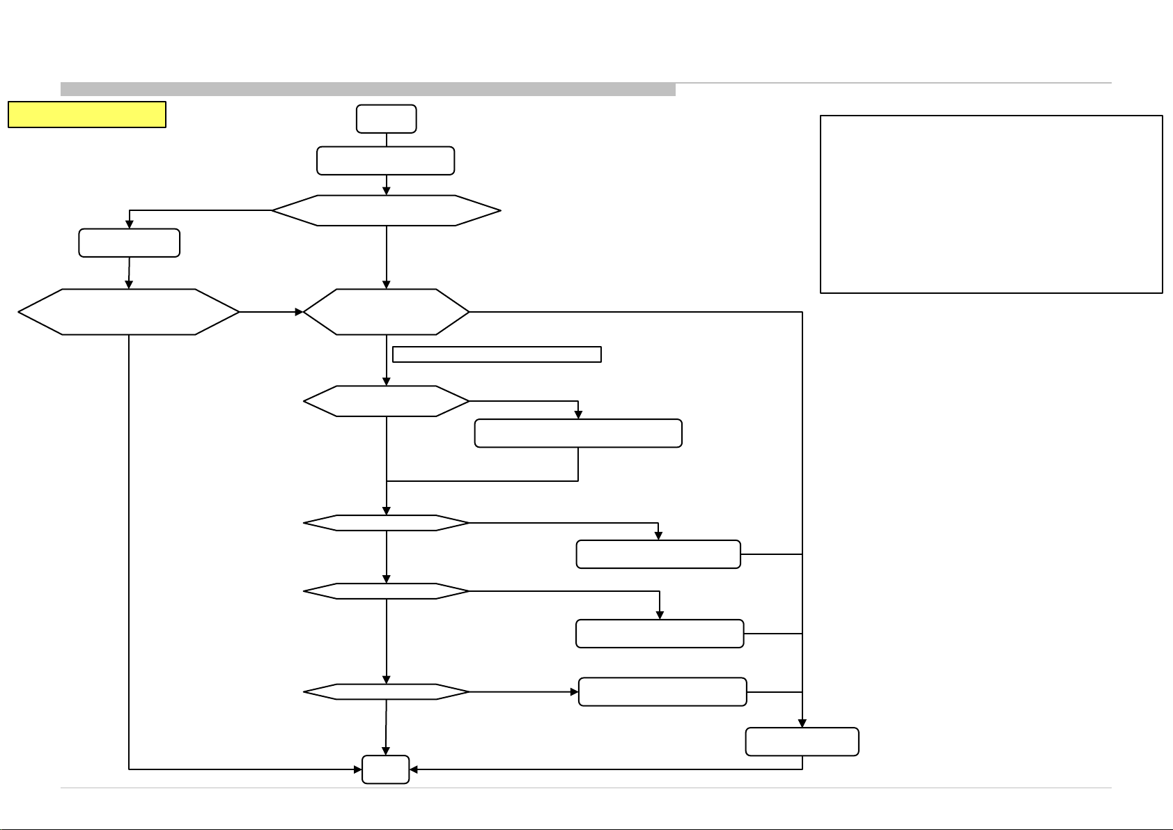
3-3-8. : USB Port2 – No Detection / Cannot Play / No Picture / No Sound
TV turn ON condition:
Change to ON
Detection OK
and
Picture and Sound OK
OK
OFF
NG
START
Do a Factory Setting
*1 Confirm USB Auto
Start is ON or OFF
ON
Check 5V at
C7021 (USB
port2)
Have 5V but No detection
*2 Confirm USB
file format
OK
Detection OK
OK
Picture OK
OK
Remarks:
*1 Confirm USB Auto Start at Set-up Menu.
*2 Confirm with OSD on bottom panel, if
playback not support.
Please refer to IM for detail supported USB
format.
*3 For model have USB Port2
No 5V
NG
Change to supported USB format
USB format OK but No detection
Hub IC (IC7001) problem
Picture NG
Main IC (IC5000) problem
Sound OK
OK
END
Sound NG
Audio IC IC4001) problem
Change B-Board
74
Page 75
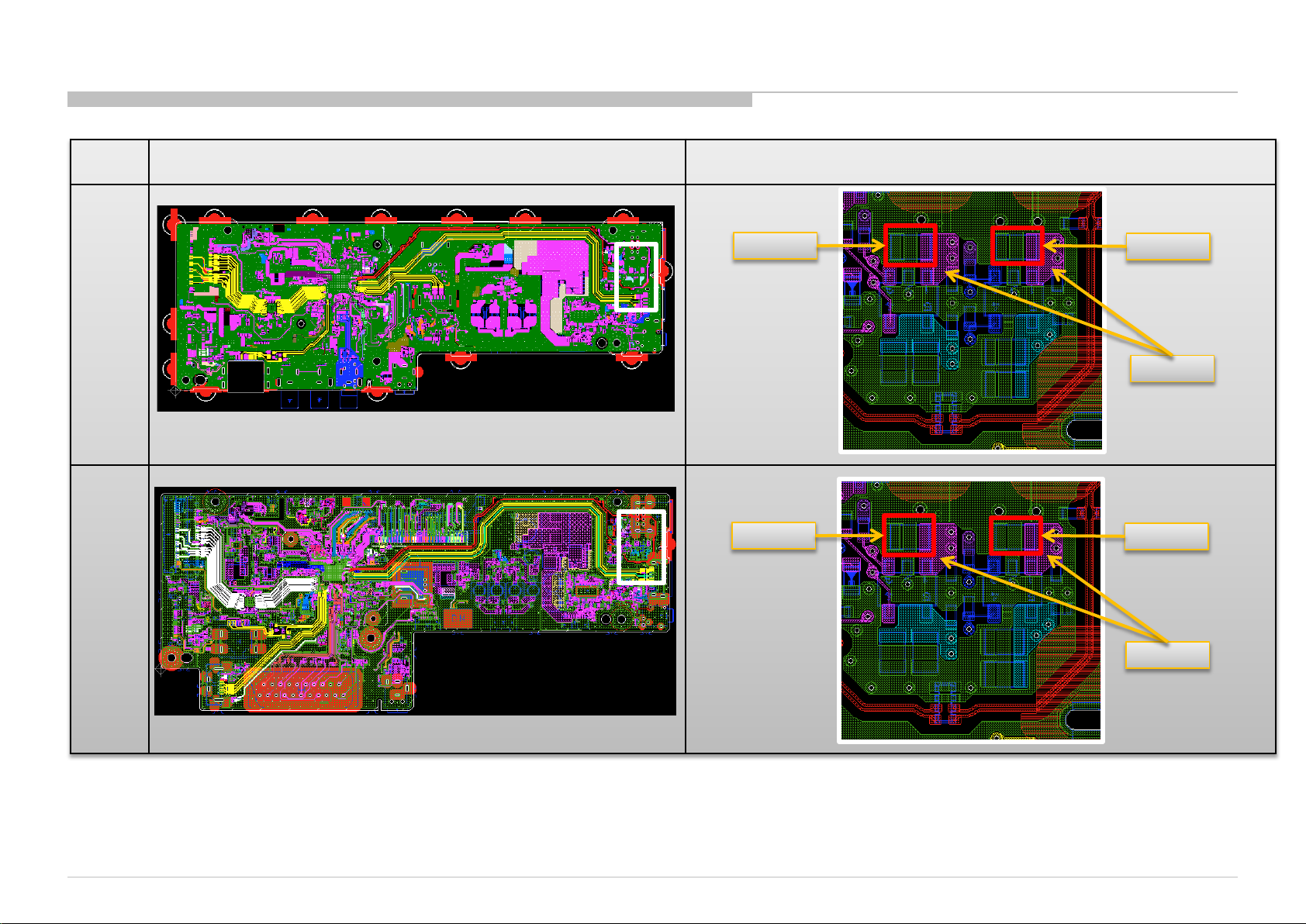
USB (B-board Checking) – Checking 5V Points [1/2]
SECTION 3
TROUBLESHOOTING
Board
Name
BBA
(QW;
QT)
BBE
(QW;
QW-L;
QT)
Board PWB (A side) Detail
C7020
C7020
C7021
Have 5V?
C7021
Have 5V?
75
Page 76
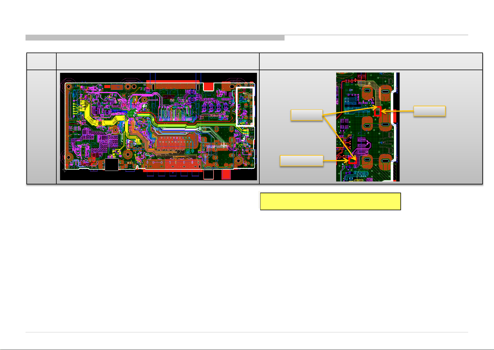
USB (B-board Checking) – Checking 5V Points [2/2]
Board
Name
BB3
(SE3;
SE3N)
Board PWB (A side) Detail
Have 5V?
(*3) C7021
Remark:
(*3) For model have USB Port2
C7020
76
Page 77
3-3-9 : Ethernet – No Connect
START
Check if TV has good
cable connection
Set-up Network setup
Failed
Check if the Ethernet
cable is good
NG
Change a good cable
TV turn ON condition:
OK
OK
Failed
Check if any abnormal
or broken point on
Ethernet Connector
No
Check if TV has MAC Address
Set-up Network setup
Yes
Yes
Connector NG
Change B Board
T7000 or T7001 or Main IC
(IC5000) NG
Change B Board
Check TV has connection OK
Set-up Network setup
OK
Failed
Invalid MAC Address
Change B Board
END
77
Page 78
3-3-10 : CI Slot – No Detection / No Picture / No Sound
START
TV turn ON condition:
Remarks:
*1 Important: Please use a known Good CICAM
for testing
Check CI
or
CI+ case
CI+
Check service menu for
CI+ Credentials CI+ Key
Invalid key
Invalid Key
Change B Board
CI
Valid key
*1 Insert Good CICAM and
Check if TV can detect CICAM
Channel Setup Digital Setup
CA Module
No
Check any pin on
CI Slot is bend or
broken.
Yes
Connector NG
Change B Board
Yes
No
Insert CICAM and
Check CI 5V
at PIN 17/18/51/52
No
IC7000 NG
Change B Board
Yes
*2 Insert CICAM and
Check CI Detection
at Pin 36/67
No
*2 Both CI Detection at Pin 36/67 should be 3.3V
before CICAM insert and 0v when CICAM
inserted.
*3 Confirm these 13 resistors part are mount
properly.
Yes
*3 Check Resistor
Part mounting
Yes
END
Power 3.3V NG
Change B Board
NG
Part Knock Off
Change B Board
Picture and
Sound OK
NG
Main IC (IC5000) NG
Change B Board
78
Yes
Page 79
CI Slot (B-board Checking) – Checking 5V Points [1/3]
Board
Name
BBE
(QW;
QW-L;
QT)
Board PWB (A side) Detail
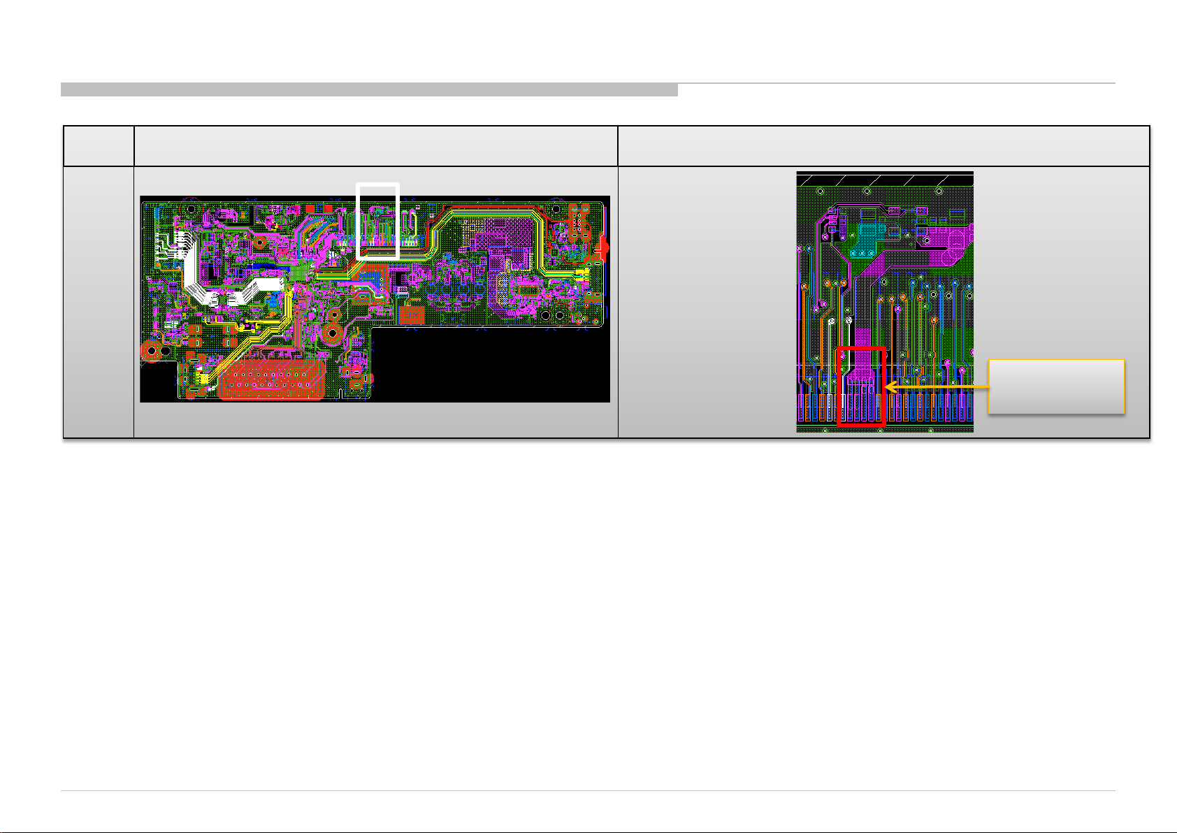
CI 5V at PIN
17/18/51/52
79
Page 80
CI slot (B-board Checking) – Checking CI Detection Pin Points [2/3]
Board
Name
BBE
(QW;
QW-L;
QT)
Board PWB (A side) Detail
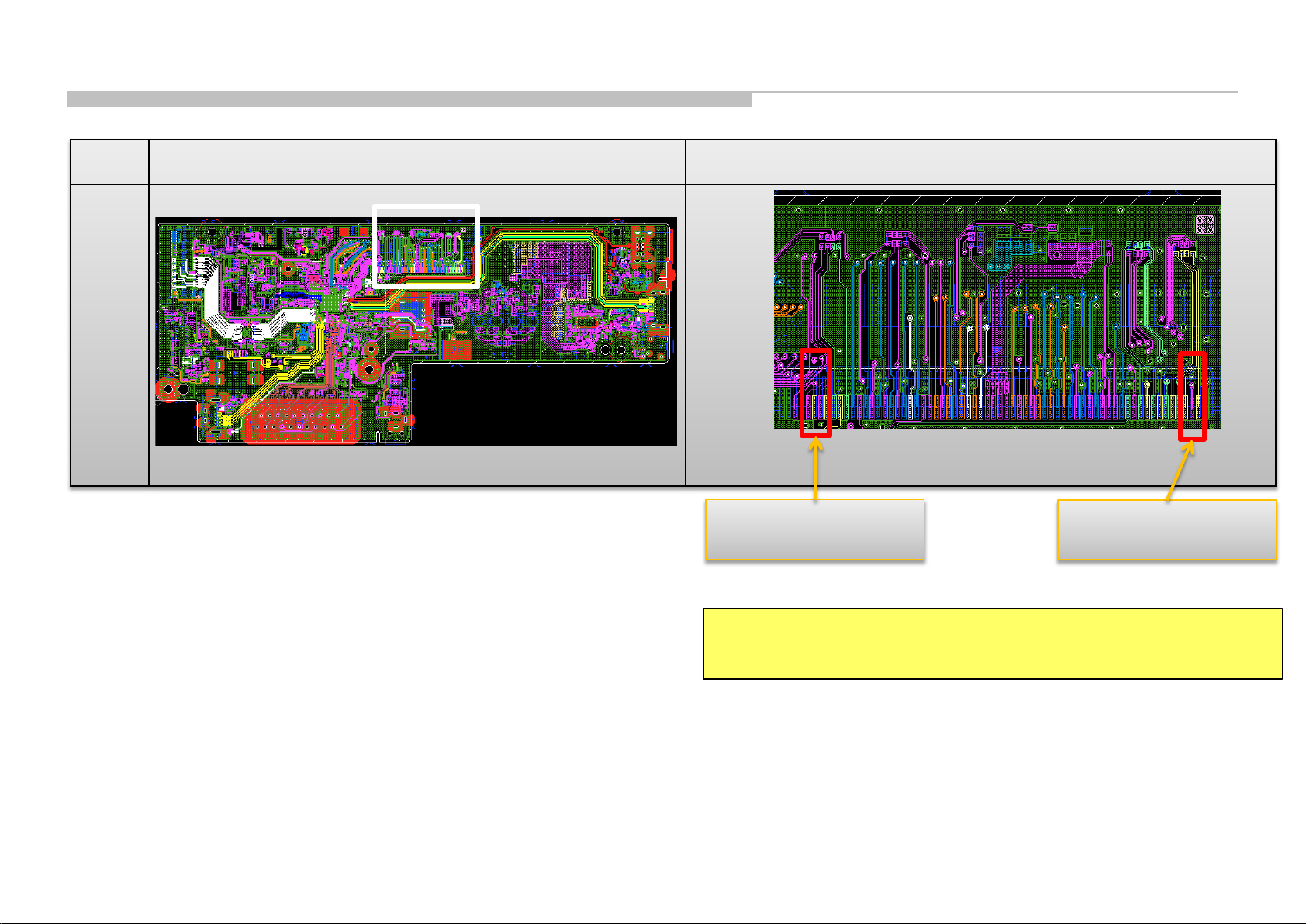
Card Detect 2 – PIN 67
Card Detect 1 – PIN 36
Remark:
Both CI Detection Pin should be 3.3V before CICAM insert and 0v when CICAM
inserted.
80
Page 81
Troubleshooting
CI slot (B-board Checking) – Checking Resistor Part Mounting Points [3/3]
Board
Name
Board PWB (A side) Detail
BBE
(QW;
QW-L;
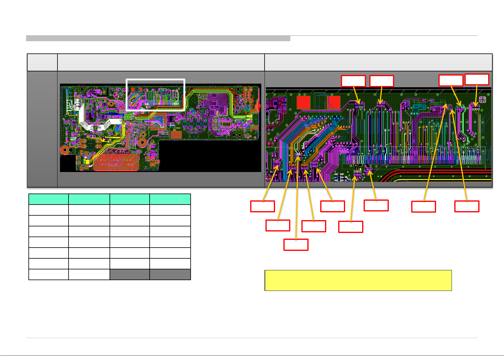
QT)
Ref. No. Location Ref. No. Location
RB7003 1 RB7010 8
RB7002 2 RB7011 9
RB7000 3 RB7008 10
8
1
2
4
5
6
9
7
12
10
11
13
RB7001 4 RB7006 11
RB7004 5 R7000 12
RB7007 6 R7001 13
RB7009 7
3
Remark:
Confirm these 13 resistors part are mount properly or not.
81
Page 82
Troubleshooting
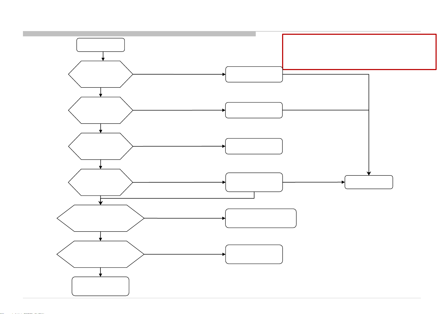
3-3-11. HDMI No Picture (a)
1. HDMI NO PICTURE
[NG] No picture
[NG] No picture
[NG] No picture
[OK] Connector no abnormality
HDMI No Picture
Verify with other
HDMI source /cable
Factory reset
HDMI source & re-verify
Verify by using laptop
Physical appearance
check on
HDMI connector
[OK] Picture recovered
[OK] Picture recovered
[OK] Picture recovered
[NG] Connector abnormal
[NG] No picture
HDMI source/
cable problem
HDMI source
setting problem
Go to
"HDCP Failure Analysis"
HDMI Connector Broken
Replace → Re-verify
Checking condition:
- TV ON & HDMI Source ON except if the flow mentioned is AC OFF.
- TV HDMI input connected to HDMI source output
- TV Input: HDMI
[OK] Picture recovered
END
Check voltage of +5V Power
HDMI1: Pin18 @ CN3601
HDMI2: Pin18 @ CN3600
[OK] Vdc = 4.8 ~ 5.3V
Check voltage of HPD
HDMI1: Pin19 @ CN3601
HDMI2: Pin19 @ CN3600
[OK] Vdc = 2.4 ~ 5.3V
“Main Flow Continue"
Go to
[NG] Vdc ≠ 4.8 ~ 5.3V
[NG] Vdc ≠ 2.4~ 5.3V
Go to
“+5V Power Failure Analysis"
Go to
“HPD Failure Analysis"
82
Page 83
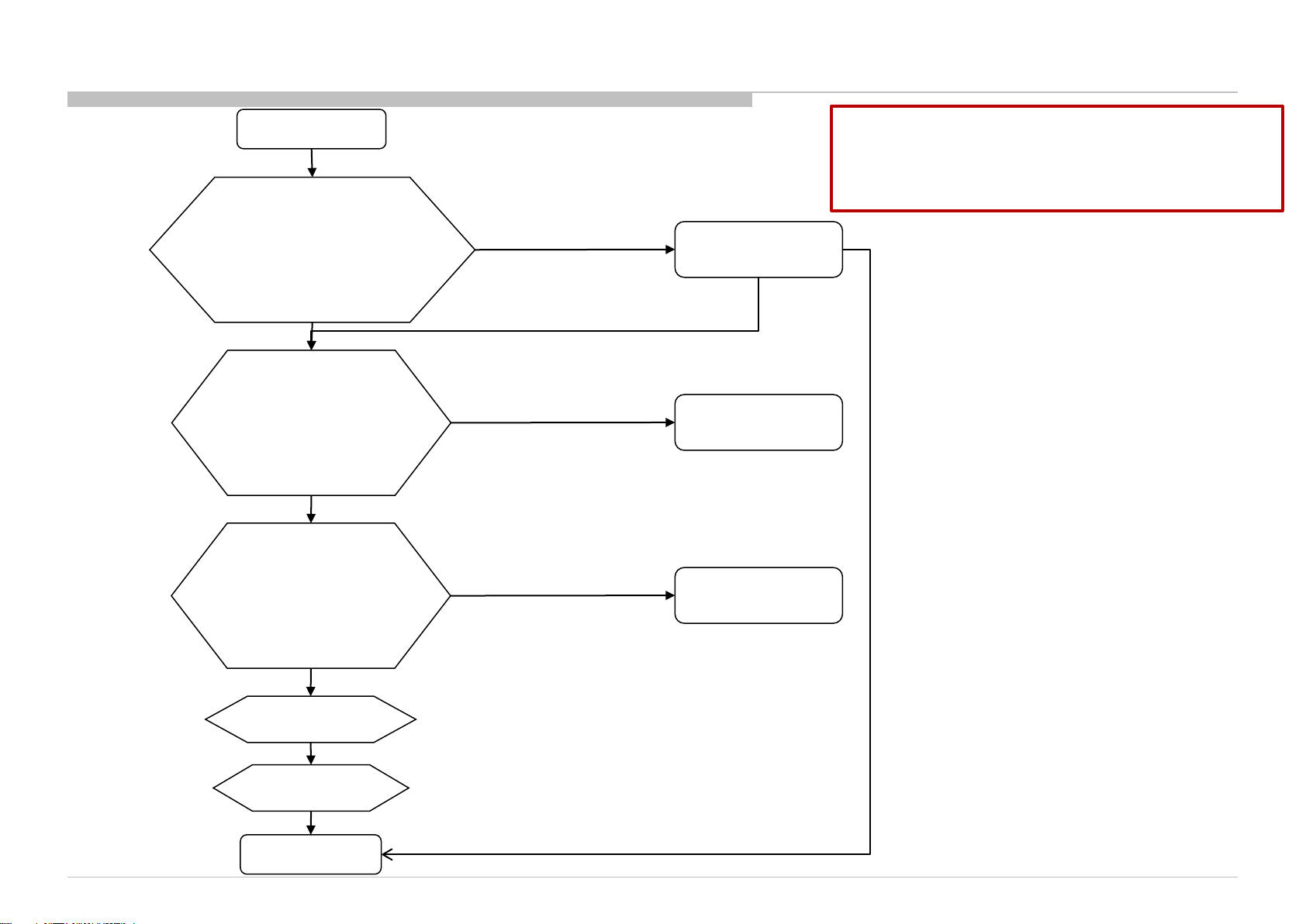
3-3-11. HDMI No Picture – Continue (b)
1. HDMI NO PICTURE
[OK] Impedance = 100Ω
Pin15 (SCL) Pin 16 (SDA) @ CN3601
Pin15 (SCL) Pin 16 (SDA) @ CN3600
[OK] Vdc = 3.5 ~ 5.5V
Main Flow Continue
Check impedance of
series resistor
at SCL & SDA
during AC OFF
HDMI1:
R3608 (SCL) & R3610 (SDA)
HDMI2:
R3618 (SCL) & R3617 (SDA)
Check voltage of SCL & SDA line
HDMI1:
HDMI2:
Check voltage @ TMDS lines
HDMI1:
Pin1,3,4,6,7,9,10 & 12 @ CN3601
HDMI2:
Pin1,3,4,6,7,9,10 & 12 @ CN3600
[NG] Impedance ≠ 100Ω
[NG] No picture
[NG] Vdc ≠ 3.5 ~ 5.5V
[NG] Vdc ≠ 2.6 ~ 3.475V
Series Resistor Broken
Replace → Re-verify
Go to
“I2C Failure Analysis"
Go to
"TMDS Failure Analysis"
Checking condition:
- TV ON & HDMI Source ON except if the flow mentioned is AC OFF.
- TV HDMI input connected to HDMI source output
- TV Input: HDMI
[OK] Picture recovered
[OK] Vdc = 2.6 ~ 3.475V
Replace B-board & re-verify
Escalate this issue to
R&D team
END
83
Page 84
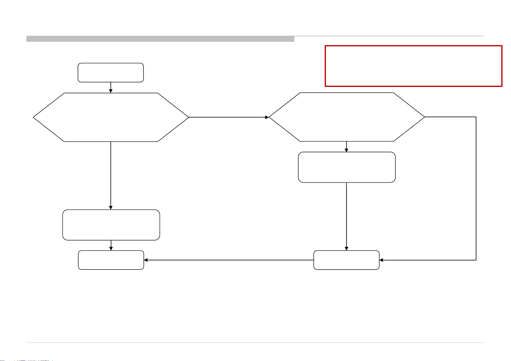
3-3-12. : HDMI No Picture – HDCP Failure Analysis
HDCP Failure Analysis
Checking condition:
- TV ON & HDMI Source ON except if the flow mentioned is AC OFF.
- TV HDMI input connected to HDMI source output
- TV Input: HDMI
Verify the HDMI source is compatible
with HDCP version 1.4
[NG] Not Compatible
HDMI Source HDCP
incompatible version
END
[OK] Compatible
Replace B-board & re-verify
[NG] No picture
[OK] Picture recovered
HDCP key corrupted
Escalate this issue to
R&D team
84
Page 85
3-3-13. HDMI No Picture – +5V Power Failure Analysis
1. HDMI NO PICTURE
+5V Power Failure
Analysis
Check impedance
of varistor during AC OFF
HDMI1: VD3607
HDMI2: VD3606
[NG] Short circuit
[OK] Open circuit
Go back to "Check
voltage of HPD"
Varistor Broken
Replace broken Varistor
& Re-verify
[OK] Picture recovered
END
[NG] No picture
Checking condition:
- TV ON & HDMI Source ON except if the flow mentioned
is AC OFF.
- TV HDMI input connected to HDMI source output
- TV Input: HDMI
85
Page 86
3-3-14 : HDMI No Picture – HPD Failure Analysis
1. HDMI NO PICTURE
HPD Failure Analysis
Check impedance of Varistor, Diode
& Resistor during AC OFF
HDMI1: VD3609, D3602, R3602, R3604 & Q3600
HDMI2: VD3608, D3601, R3601, R3644, R3620 &
[NG] Any of the part as below
VD3609, VD3608: = Short circuit
R3602,R3601: ≠ 33Ω
R3604,R3620: ≠ 1KΩ
R3644: ≠ 0Ω
Q3600, Q3611: V
CE = Short
Q3611
[OK] All the part as below
VD3609, VD3608: ≠ Short circuit
R3602,R3601: = 33Ω
R3604,R3620: = 1KΩ
R3644: = 0Ω
Q3600, Q3611: V
CE = Open
[NG] short Circuit / Low impedance
[OK] Picture recovered
Checking condition:
- TV ON & HDMI Source ON except if the flow mentioned is AC OFF.
- TV HDMI input connected to HDMI source output
- TV Input: HDMI
Check HPD GPIO Line Short to Ground
during AC OFF
HDMI1: Pin 19 @ CN3601
HDMI2: Pin 19 @ CN3600
Internal Main SoC (IC5000) broken
Replace B-board & re-verify
[OK] Open Circuit
Varistor/Diode/Resistor/
Transistor is broken
Replace the Broken Varistor/
Diode/Resistor & Re-verify
[OK] Picture recovered
END
[NG] No picture
[NG] No picture
Escalate this issue to
R&D team
Go back to "Check
impedance of serial
resistor at SCL & SDA
during AC OFF""
86
Page 87
3-3-15 : HDMI No Picture – I2C Failure Analysis
1. HDMI NO PICTURE
I2C Failure Analysis
Checking condition:
- TV ON & HDMI Source ON except if the flow mentioned is AC OFF.
- TV HDMI input connected to HDMI source output
- TV Input: HDMI
Check impedance of network resistor
during AC OFF
HDMI1: RB3608
HDMI2: RB3611
[NG] Impedance ≠ 47KΩ
Network resistor broken
Replace network resistor
& Re-verify
Check SCL & SDA GPIO Line Short to Ground
[OK] Impedance ≈ 47KΩ
[OK] Open Circuit (≈ 100kΩ)
HDMI1: Pin15 (SCL) ,Pin 16 (SDA) @ CN3601
HDMI2: Pin15 (SCL) ,Pin 16 (SDA) @ CN3600
[NG] short Circuit / Low impedance
Internal Main SoC (IC5000) broken
[OK] Picture recovered
Replace B-board & re-verify
[NG] No picture
Escalate this issue to
R&D team
Go back to "Check
voltage at TMDS lines"
[NG] No picture
[OK] Picture recovered
END
87
Page 88
3-3-16 : HDMI No Picture – TMDS Failure Analysis
1. HDMI NO PICTURE
TMDS Failure Analysis
Checking condition:
- TV ON & HDMI Source ON except if the flow mentioned is AC OFF.
- TV HDMI input connected to HDMI source output
- TV Input: HDMI
Check impedance of network resistor
, serial resistor and CMF(Filter) during
AC OFF
HDMI1 : RB3600,RB3601,RB3604,RB3605
HDMI2 : RB3602,RB3603,RB3606,RB3607
,R3622,R3623
[NG] Impedance ≠ 0Ω
Network resistor/serial
resistor/ CMF broken
Replace Network resistor/
serial resistor/CMF & Re-verify
[OK] Impedance ≈ 0Ω
[NG] No picture
Check TMDS GPIO Line Short to Ground
HDMI1: Pin1, 3, 4, 6, 7, 9, 10 & 12 at CN3601
HDMI2: Pin1, 3, 4, 6, 7, 9, 10 & 12 at CN3600
[NG] short Circuit / Low impedance
Internal Main SoC (IC5000) broken
[OK] Picture recovered
Replace B-board & re-verify
during AC OFF
[NG] No picture
Escalate this issue to
R&D team
[OK] Open Circuit
[OK] Picture recovered
END
88
Page 89
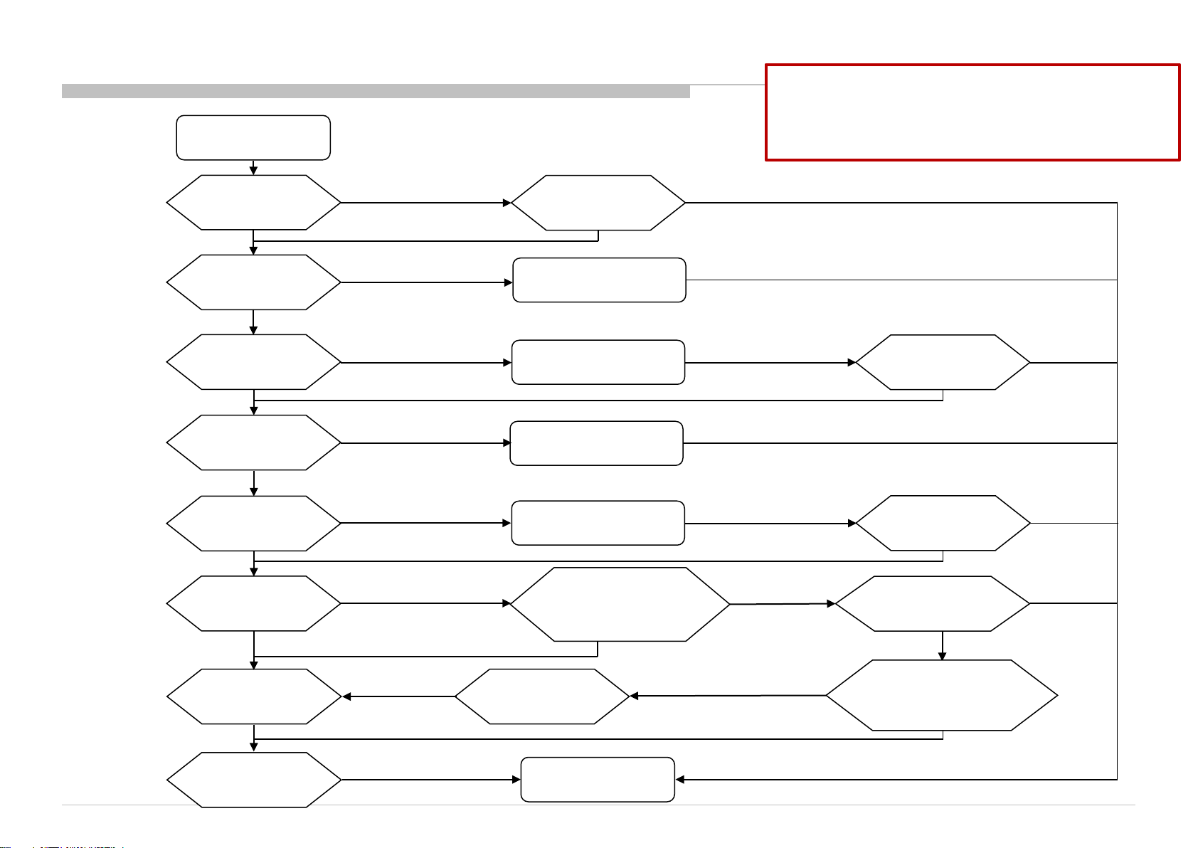
3-3-17 : CEC Not Function- Bravia Sync (CEC) not function- HDMI
Bravia Sync (CEC)
Not Function
Checking condition:
- TV ON & HDMI Source ON except if the flow mentioned is AC OFF.
- TV HDMI input connected to HDMI source output
- TV Input: HDMI
Check CEC BRAVIA Sync
Device List "Enable"
[NG] No CEC device list
Source side Support CEC
[OK] Support CEC
Check Source and TV
CEC/BRAVIA Sync setting
[OK] Setting is "ON"
Change other HDMI
cable that proven OK
& Re- Verify
[NG] CEC not function
Physical appearance
check on HDMI connector
[OK] Connector no abnormality
Check voltage at CEC pin
[OK] Voltage ≈ 2.5~3.63V
Replace B-board &
re-verify
[OK] Source device listed
[NG] CEC not function
[NG] Not Support CEC
[OK] Setting is "OFF"
[OK] CEC functioning
[NG] Connector abnormal
[NG] Voltage ≠ 2.5~3.63V
[OK] VD: Open circuit, R3613: ≈100Ω
Internal Main SoC
(IC5000) broken
Make Factory reset
To Source and TV "
Source side not
support CEC
Source and TV CEC
setting problem
Customer HDMI cable
problem
HDMI connector broken
Check impedance of
varistor &
resistor during AC OFF
VD3601, VD3600 & R3613
[OK] CEC functioning
[NG] CEC not function
[NG] CEC not function
[NG] VD: Short circuit,
R3613: ≠100Ω
[NG] short Circuit /
Low impedance
[OK] Open Circuit
Turn to “ON” CEC
Setting & Re-verify
Replace HDMI
Connector & Re-verify
Replace varistor & resistor
& Re-verify
[NG] CEC not function
Check CEC GPIO
Line Short to Ground
During AC OFF
Pin 13 @ CN3600/CN3601
[OK] CEC functioning
[OK] CEC functioning
[OK] CEC functioning
Escalate this issue
to R&D team
END
89
Page 90
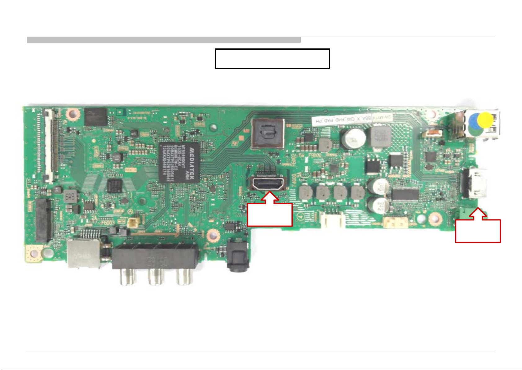
HDMI No Picture- Checking Point[1/8]
QW – BBA (Side A)
HDMI1
(CN3601)
HDMI2
(CN3600)
90
Page 91
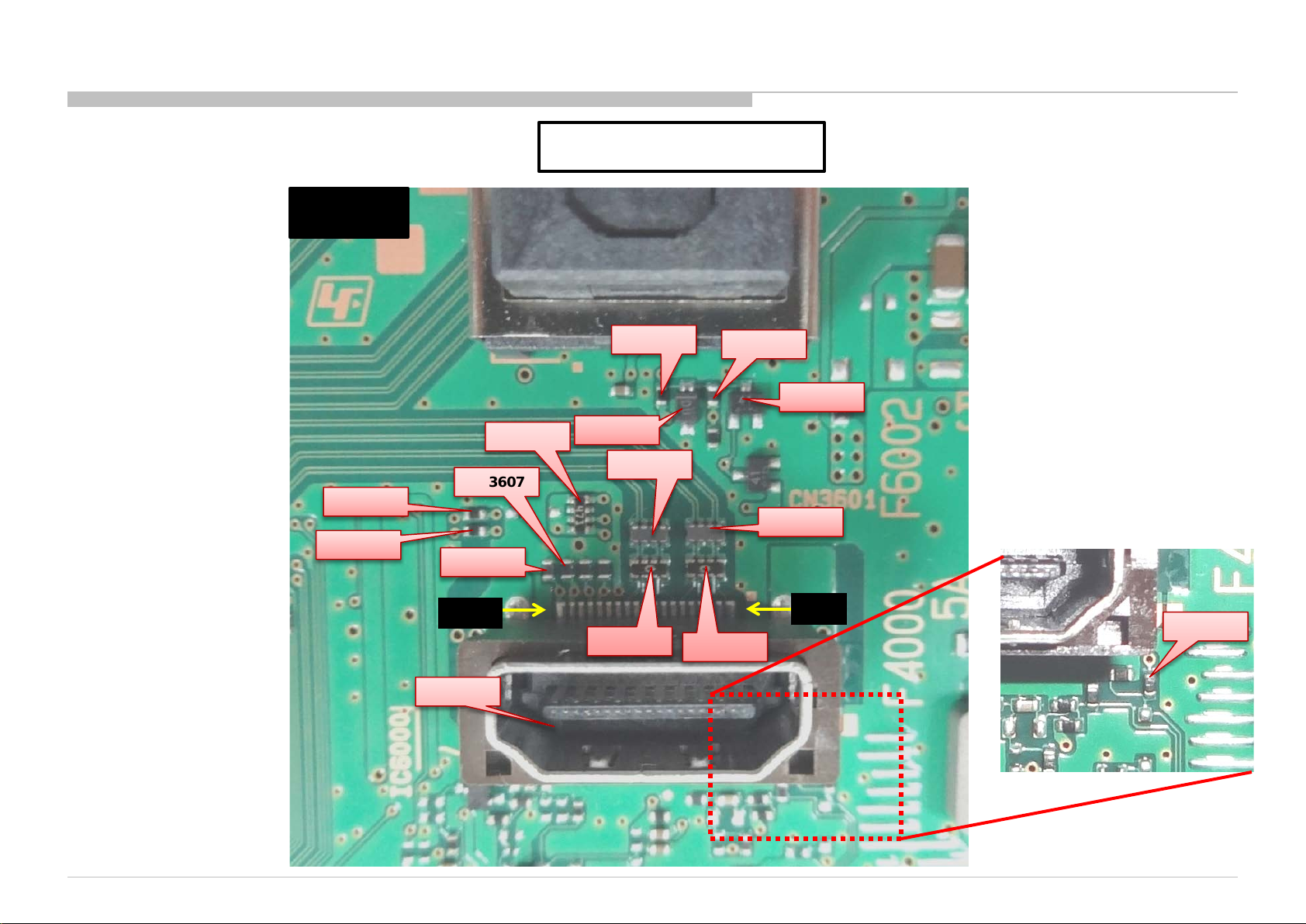
HDMI No Picture- Checking Point[2/8]
HDMI1
QW – BBA (Side A)
R3608
R3610
VD3607
VD3609
Pin 19
CN3601
RB3608
R3604
D3602
RB3605
RB3601
R3602
Q3600
RB3604
Pin 1
CN3601
RB3600
91
Page 92
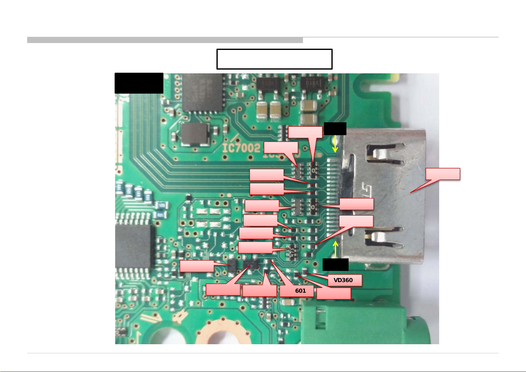
HDMI No Picture- Checking Point[3/8]
HDMI2
QW – BBA (Side A)
D3601
Q3611
R3622
R3623
RB3607
R3618
R3617
RB3611
R3644
RB3606
R3601
RB3602
Pin 1
CN3600
RB3603
VD3608
Pin 19
VD3606
R3620
92
Page 93
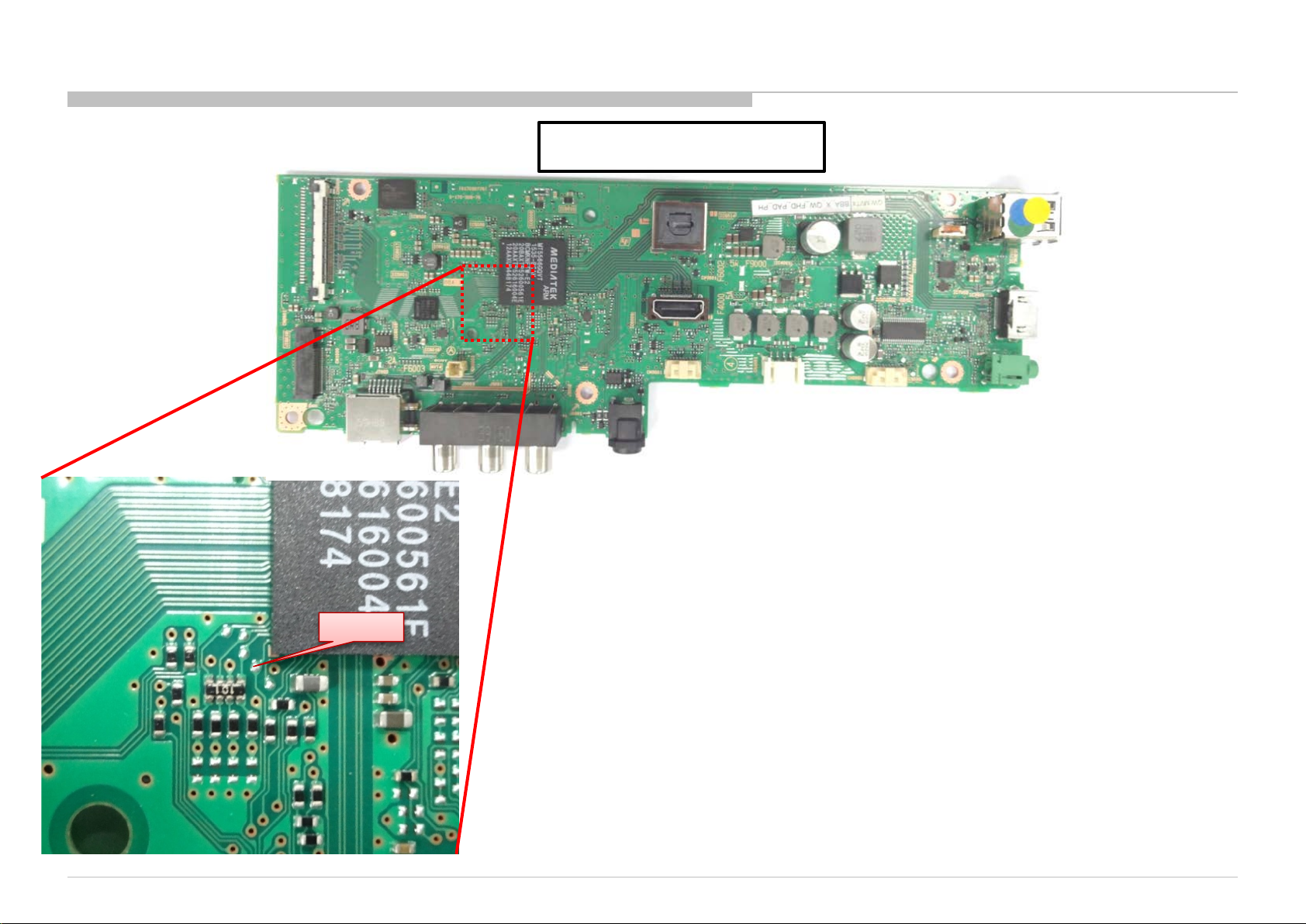
HDMI No Picture- Checking Point[4/8]
QW – BBA (Side A)
CL5007
93
Page 94
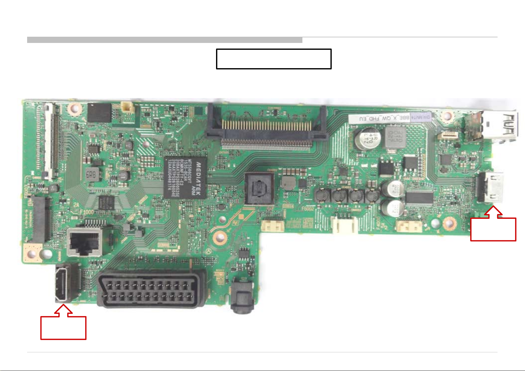
HDMI No Picture- Checking Point[5/8]
QW – BBE (Side A)
HDMI1
(CN3601)
HDMI2
(CN3600)
94
Page 95
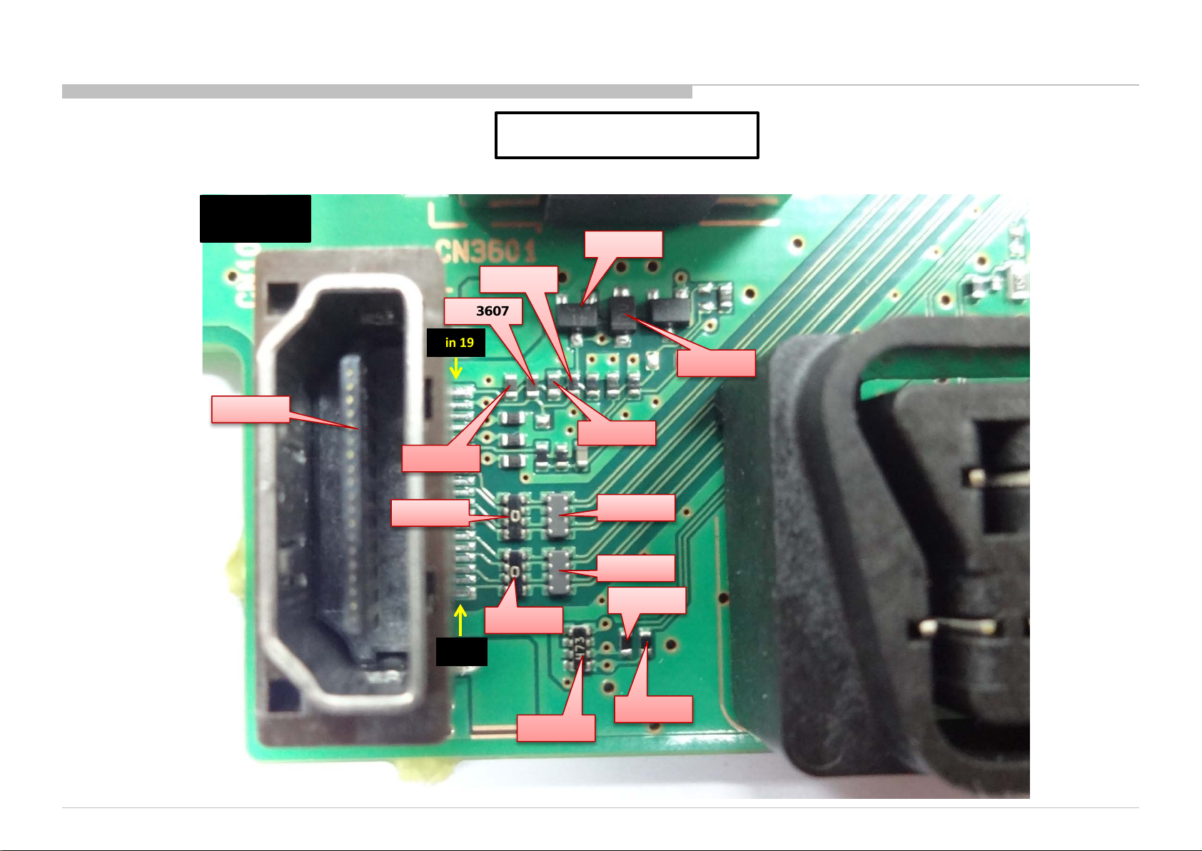
HDMI No Picture- Checking Point[6/8]
HDMI1
CN3601
QW – BBE (Side A)
Q3600
R3604
VD3607
Pin 19
D3602
R3602
VD3609
RB3601
Pin 1
RB3605
RB3604
R3610
RB3600
R3608
RB3608
95
Page 96
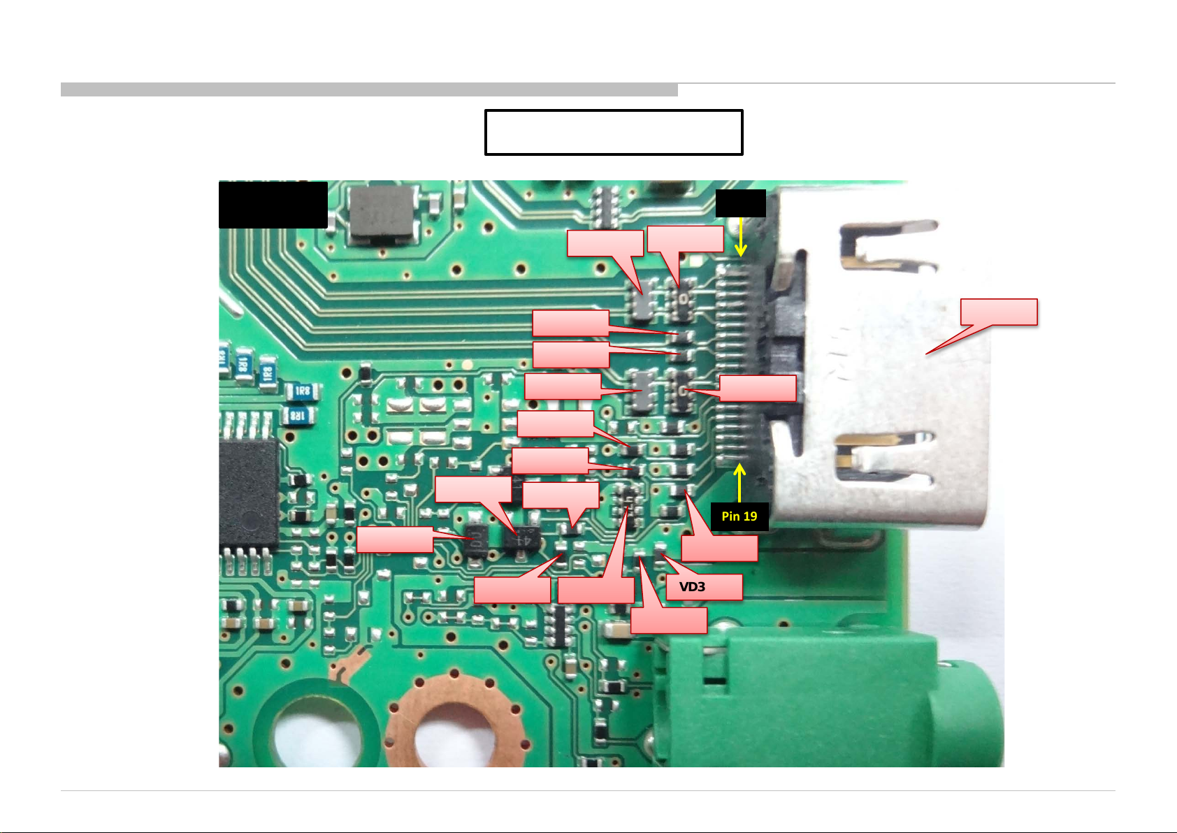
HDMI No Picture- Checking Point[7/8]
QW – BBE (Side A)
HDMI2
D3601
Q3611
R3644
R3622
R3623
RB3607
R3618
R3617
R3601
RB3606
RB3611
Pin 1
RB3602
CN3600
RB3603
Pin 19
VD3608
VD3606
R3620
96
Page 97
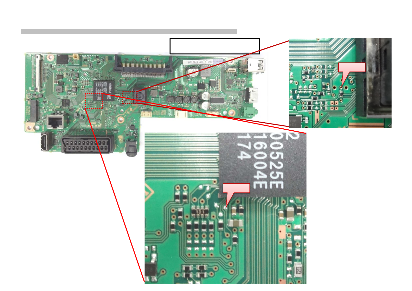
HDMI No Picture- Checking Point[8/8]
QW – BBE (Side A)
R3613
CL5007
97
Page 98
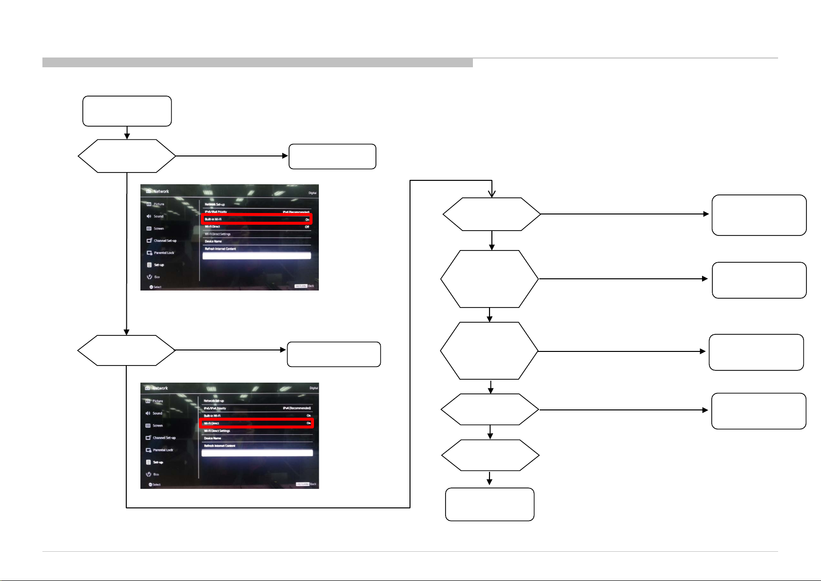
3-3-19. WiFi- Cannot Search Device - Connection Failed
Start
Connection Failed
Check Built-In WiFi
UI
OK
Check WiFi Direct
UI
OK
NG: Built-In WiFi Off
NG: WiFi Direct Off
WiFi Feature is
Not Enable
WiFi Direct Feature is
Not Enable
Check STBY_5V
Q9901
OK
Check Harness
Connection
CN9900
OK
Check TP-VCC
J20H090
OK
Check AP/Device
OK
Change B*Board /
WiFi Module
NG: DC Voltage not 5V
NG: Harness Connection Not Ok
NG: DC Voltage is not 5V
NG: Signal Strength Low
Mosfet Q9901
Broken
(Change B*Board)
Harness not in
Good Condition
(Change Harness)
WiFi Module
J20H090 Broken
(Change WiFi Module)
AP Device
Problem
(Change AP/Device)
OK
END
Connection Success
98
Page 99
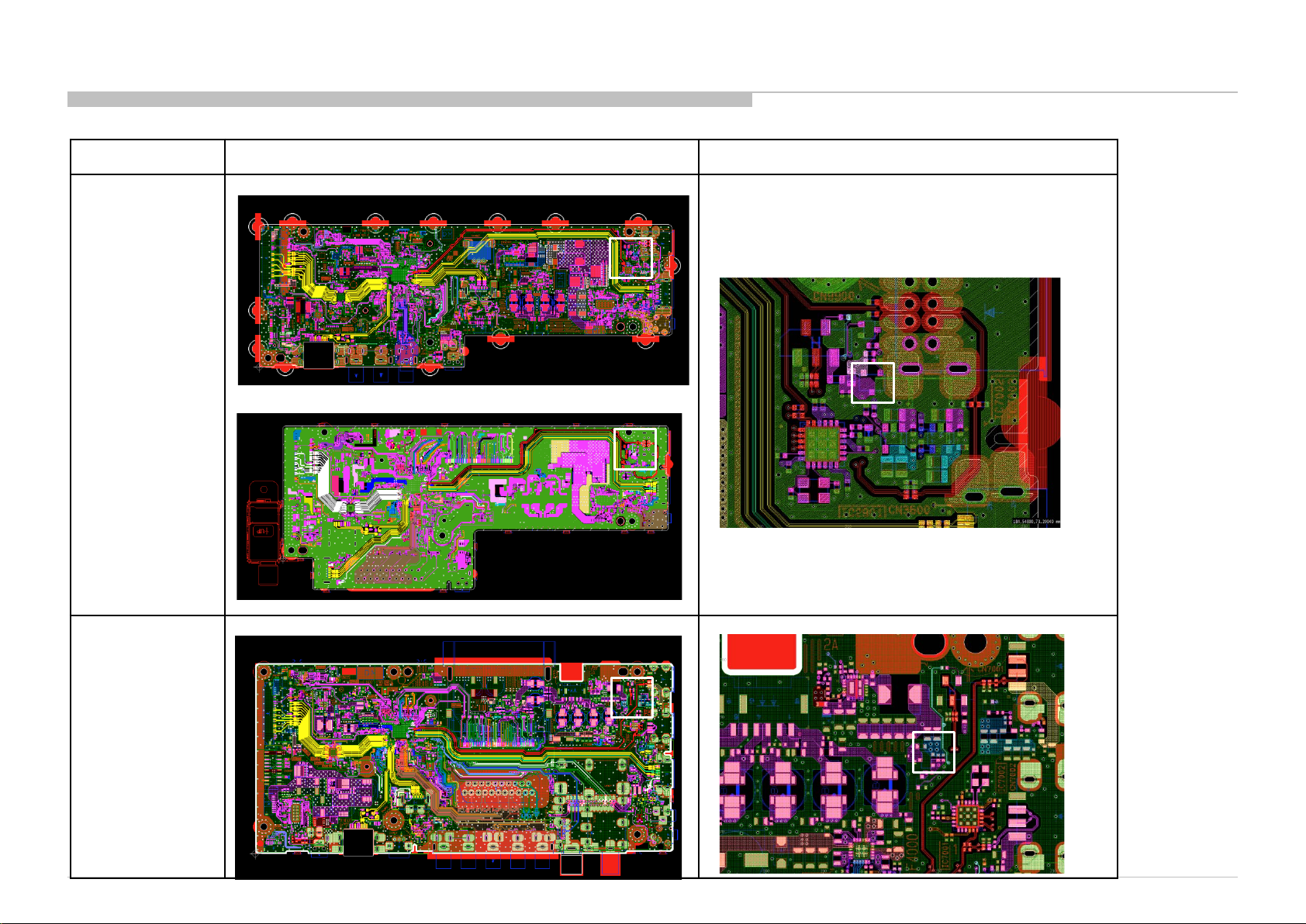
WiFi- Cannot Search Device - Connection Failed – Checking Point [1/2]
Board Name Board PWB (A side) Detail
B*Board
(BBA,BBE)
Q9901
B*Board
(BB3)
Q9901
BBA
BBE
Q9901
Q9901
Q9901
Q9901
Q9901
99
Page 100
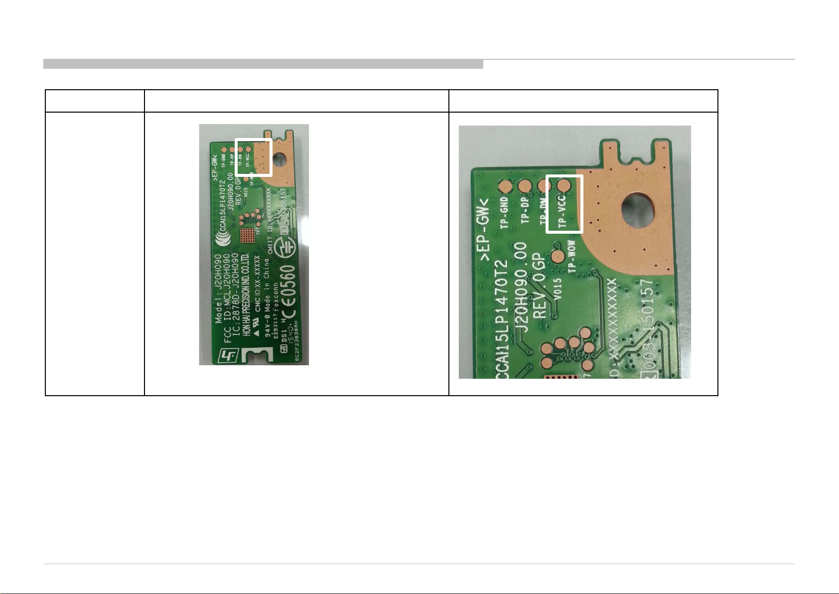
WiFi- Cannot Search Device - Connection Failed – Checking Point [2/2]
Board Name Board PWB (B side) Detail
WiFi Module
J20H090
TP-VCC
TP-VCC
100
 Loading...