

Page 1

KDE55XBR950
UC Model
PANEL MODULE SERVICE MANUAL
PDP Module Name
FPF55C17196UA
FLAT PANEL COLOR TV
Page 2

CONTENTS
1 OUTLINE ..................................................................................................................................1
1.1 Panel Dimension ................................................................................................................1
1.2 Feature...............................................................................................................................1
1.3 Specification .......................................................................................................................2
1.3.1 Functional specification ...............................................................................................2
1.3.2 Display quality specification.........................................................................................3
1.3.3 I/O Interface Specification............................................................................................ 4
2 SAFETY HANDLING of THE PLASMA DISPLAY ..................................................................... 8
2.1 Notes to Follow During Servicing ....................................................................................... 8
3 NAME and FUNCTION .............................................................................................................9
3.1 Configuration ......................................................................................................................9
3.2 Block Diagrams ................................................................................................................10
3.2.1 Signal Diagrams ........................................................................................................10
3.2.2 Power Diagrams ........................................................................................................ 11
3.3 Function............................................................................................................................12
3.3.1 Logic board Function .................................................................................................12
3.3.2 Function of X-SUS Board ..........................................................................................13
3.3.3 Function of Y-SUS Board........................................................................................... 13
3.4 Protection function............................................................................................................14
4 PROBLEM ANALYSIS ............................................................................................................15
4.1 Outline of Repair Flow......................................................................................................15
4.2 Outline of PDP Module Repair Flow.................................................................................16
4.3 Checking the Product Requested for Repair....................................................................19
4.4 Operation Test Procedure ................................................................................................20
4.5 Fault Symptom .................................................................................................................22
4.6 Problem Analysis Procedure ............................................................................................ 25
4.6.1 "The entire screen does not light.(Main power is turned off)” Problem analysis
procedure............................................................................................................................25
4.6.2 "Vertical line/Vertical bar" Problem analysis procedure.............................................. 31
4.6.3 "Horizontal bar" Problem analysis procedure.............................................................35
4.7 Problem Analysis Using a Personal Computer................................................................. 36
4.7.1 Connecting a computer..............................................................................................36
4.7.2 Preparing a computer ................................................................................................36
4.7.3 Problem Analysis Procedure...................................................................................... 37
5 Disassembling and Reassembling..........................................................................................40
5.1 Exploded View..................................................................................................................40
5.2 X-SUS Circuit Board Removal/Installation Procedure......................................................41
Page 3

5.3 Y-SUS Circuit Board Removal/Installation Procedure................................................................43
5.4 ABUS-U1 Circuit Board Removal/Installation Procedure.......................................................... 45
5.5 ABUS-U2 Circuit Board Removal/Installation Procedure.......................................................... 47
5.6 ABUS-U3 Circuit Board Removal/Installation Procedure .......................................................... 49
5.7 ABUS-U4 Circuit Board Removal/Installation Procedure .......................................................... 51
5.8 ABUS-D1 Circuit Board Removal/Installation Procedure..........................................................53
5.9 ABUS-D2 Circuit Board Removal/Installation Procedure..........................................................55
5.10 ABUS-D3 Circuit Board Removal/Installation Procedure........................................................ 57
5.11ABUS-D4 Circuit Board Removal/Installation Procedure.........................................................59
5.12 LOGIC Board Removal/Installation Procedure......................................................................... 61
5.13 Complete Panel Chassis Removal/Installation Procedure......................................................63
6 Operation Check and Adjustment Method..........................................................................................66
6.1 List of Check and Adjustment Items.............................................................................................66
6.2 Check and Adjustment Method.....................................................................................................67
6.2.1 Check and adjustment procedure.........................................................................................67
6.2.2 Parameter adjustment............................................................................................................68
6.2.3 Operation performance check items.....................................................................................70
6.2.4 Heat Run Test...........................................................................................................................72
6.2.5 Logic board parameter forwarding .......................................................................................74
6.2.6 Accumulation time reset.........................................................................................................76
6.2.7 Setup before shipment...........................................................................................................77
7 The parts information .............................................................................................................................78
7.1 FPF55C17196UA-53 configuration list.......................................................................................78
8 packing Procedure................................................................................................................................79
8.1 Single packing................................................................................................................................ 79
Page 4

Caution
Scope; 55P1 series
(Model name; FPF55C17196UA)
Before doing the service operation please be sure to read this service
analysis manual. This module has a lot of devices to secure the safety
against the fire, electric shock, injury and harmful radiation.
To maintain the safety control, please follow the instructions and remarks
described in this service analysis manual.
Page 5
)
1 OUTLINE
The module is a plasma display module which can be designed in there is no fan in addition to a
general feature of the plasma display such as a flat type, lightness, and high-viewing-angle and
terrestrial magnetism.
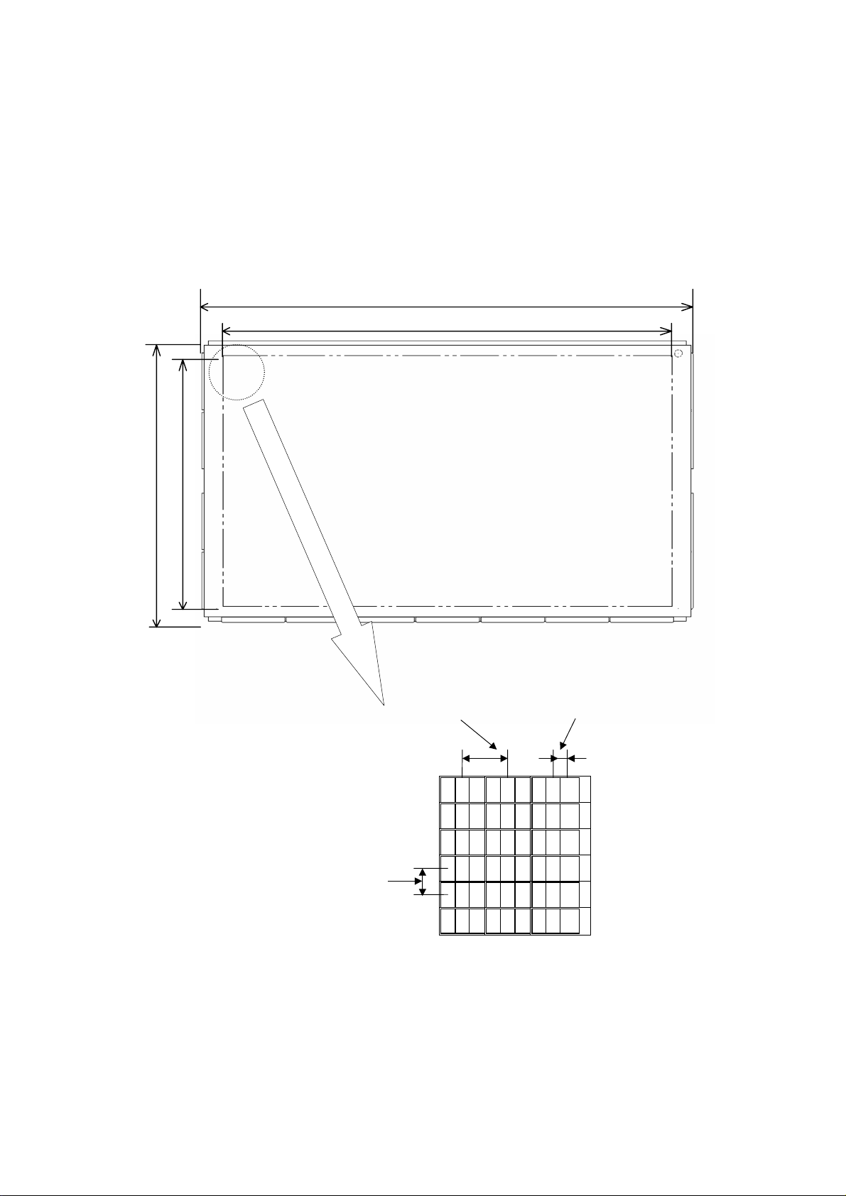
1.1 PANEL DIMENSION
1340(Glass
1229.4
691.2
750(Glass)
Pixel pitch(horizontal)
Pixelpitch(Vertical)
0.90mm
RGB
RGB
RGB
RGB
RGB
RGB
0.90 mm
RGB
RGB
RGB
RGB
RGB
RGB
1.2 FEATURE
1. For high definition television and monitor by Progressive method
2. For FAN Less design(Low consumption electric power)
3. Flat type・Lightness
4. Customizing of module equipped with communication function
-1-
Sub- pixel pitch(horizontal)
0.30mm
RGB
RGB
RGB
RGB
RGB
RGB
Page 6

1.3 SPECIFICATION
1.3.1 Functional specification
Item NO
Specification
UA-5*
Externals
Display panel
Color Grayscale(standard)
BrightNess
Chromaticity
Coordinates
Contrast Contrast in Darkroom(60Hz)
Data signal
Module size
Weight
Display size
Resolution
Pixel pitch
Sub pixel pitch
White(display load Ratio 1%,standard)
(x,y)、white 10%
Video signal (RGB each color)
1 1340 × 760 × 66mm
2 30kg
3 1229.4 × 691.2mm
(55inch: 16:9)
4 1366 × 768 pixel
5 0.90(H) × 0.90(V)mm
6 0.30(H) × 0.90(V)mm
9 RGB each color 256 Grayscale
11 1000cd/ m2
14 (0.290,0.290)
15 900:1
16 LVDS(10bit)X1 or LVDS(10bit)X2
Dot clock(max)
Sync Signal
Powersupply
Noise Shade noise at 18dB(A) or less
Guarantee
environment
Horizontal Sync Signal(max)
Vertical Sync Signal
Input voltage/current
Standby electric power(max)
Temperature(operation)
Temperature(storage)
Humidity(operation)
Humidity(storage)
17 85MHz
18 50KHz(LVDS)
19 50Hz ± 1.9 / 60 ± 1.7Hz (LVDS)
20 +3.3/+5/+75-90/+50-65V
21 1W
22 25dB(A) or less
23
24
25 20 ~ 85 %RH (no condensation)
26 20 ~ 80 %RH (no condensation)
0 ~ 45 °C
0 ~ 45 °C
*It is made to give priority when there is a delivery specification according to the customer.
DC, 0.05/7.5/7.5/6A
-2-
Page 7
1.3.2 Display quality specification
Specification
Item NO
UC-5*
Non-lighting cell
defect
Non-extinguishing
cell defect
Flickering cell defect
High intensity cell
defect
Brightness variation
Color variation White block of 10% load [9 point]
Total number (subpixel)
Density (subpixel/cm2)
Size (H x V) (subpixel)
Total number (subpixel)
Density (subpixel/ cm
Flickering lighting cell defect
(sub pixel/cm
Flickering non-extinguishing cell defect
Twice or more bright point
White block of 10% load [9 point] (%)
In area adjacent 20mm [White] (%)
2
)
2
)
1 15 or less
2 2 or less
(However,1 continuousness or less)
3 1x2 or less, Or 2x1 or less
4
5 Each color 2 cells max
6 5 or less
7 Number on inside of
8 0
9 20 or less
10 10 or less
11 X: Average ± 0.020
6 or less(each color 2 or less)
(However,1 continuousness or less)
Non-extinguishing cell defect
y: Average ± 0.020
*It is made to give priority when there is a delivery specification according to the customer.
-3-
Page 8

A
1.3.3 I/O Interface Specification
(1) LVDS Signal Definition and Function
A video signal (display data signal and control signal) is converted from parallel data to serial
data with the LVDS transmitter and further converted into four sets of differential signals before
input to this product. These signals are transmitted seven times faster than dot clock signals.
The dot clock signal is converted into one set of differential signals by the transmitter before
input to this product. The LVDS signal definition and function are summarized below:
No. Item Signal Name
Number
of
signals
I/O Form Content of definition
1
Video Signal
Timing Signal
(ODD)
2
Video Signal
Timing Signal
(EVEN)
Display signal
3
4
5
6 SDA 1 I/O
Clock (ODD)
Clock (EVEN)
Power down
Signal
Communication
7
RA0RA0+
RA1RA1+
RA2RA2+
RA3RA3+
RA4R
4+
RB0RB0+
RB1RB1+
RB2RB2+
RB3RB3+
RB4RB4+
RACLKINRACLKIN+
RACLKINRACLKIN+
PDWN 1 Input LVTTL
SCL 1 I/O
1
1
1
1
1
1
1
1
1
1
1
1
1
1
1
1
1
1
1
1
1
1
1
1
Input
Input
Input
Input
LVDS
Differential
LVDS
Differential
LVDS
Differential
LVDS
Differential
LVTTL
2
(I
C)
Differential serial data signal.
Input video and timing signals after
differential serial conversion using a
dedicated transceiver.
The serial data signal is transmitted
seven times faster than the base
signal.
Differential serial data signal.
Input video and timing signals after
differential serial conversion using a
dedicated transceiver.
The serial data signal is transmitted
seven times faster than the base
signal.
Input the clock signal after
differential conversion using a
dedicated transceiver.
The clock signal is transmitted at
the same speed as the base signal.
Low :LVDS receiver outputs are all
“L”.
High: Output signals are active.
2
I
C bus serial data communication
signal.
Communication with the control
MPU of this product is enabled.
“High”: Low power consumption
8
9
10
Control
MPU Communication / Control
CPUGO 1 Input LVTTL
PDPGO 1 Input LVTTL
IRQ 1
Outpu
t
LVTTL
mode of the control MPU of this
product is released.
“High”: This product is started.
(CPUGO=“High” Effective)
It changes into "Low" → "High"
when this product enters the
undermentioned state.
1. Vcc/Va/Vs output decrease
2. Circuit abnormality detection
-4-
Page 9

A
B
(2) Video Signal Definition and Function
The table below summarizes the definitions and functions of input video signals before LVDS
conversion.
Item Signal name
Original
Display signal
(before LVDS
transmittance)
Video signal
(ODD)
Video signal
(EVEN)
Clock
Horizontal
sync signal
Vertical sync
signal
Blanking
signal
DATA-RA
DATA-GA
DATA-BA
DATA-RB
DATA-GB
DATA-BB
DCLK
DCLK
Hsync
Vsync
BLANKA
BLANKB
Number
of signals
Input/
output
10
10
10
10
10
10
2 Input
1 Input
1 Input
2 Input
Input
Input
Display data signal
RA9/GA9/BA9 is the highest intensity bit.
RA0/GA0/BA0 is the lowest intensity bit.
Display data signal
RB9/GB9/BB9 is the highest intensity bit.
RB0/GB0/BB0 is the lowest intensity bit.
Video signal timing: These signals
continuously input are necessary. Data are
read when these signals are fallen.
Regulates one horizontal line of data: Begins
control of the next screen when
fallen.
Screen starts up control timing signal: Begins
control of the next screen when
fallen.
Input the same frequency in both
odd-numbered and even-numbered fields.
Display period timing signal.
H indicates the display period and L indicates
the non display period.
Note:
Set this timing properly like followings, as is
used internally for signal processing.
・Set the blanking period so that the number of
effective display data items in one horizontal
period is 1366.
・Set the number of blanking signals in one
vertical period to 384, which is one half the
number of effective scan lines.
Signal definition and function
Hsync is
Vsync is
If the
BLANK changes when the Vsync
frequency is switched, the screen display may
be disturbed or brightness may change.
The screen display is restored to the normal
state later when the
constant again.
BLANK length is
-5-
Page 10

)
)
(3) Connector Specification
The connector specification is shown below. Please do not connect anything with the terminal NC.
(3-1) Signal connector [CN1]
Pin No. Signal name Pin No. Signal name
1 RA0- 2 GND(LVDS
3 RA0+ 4 SCL
5 RA1- 6 GND
7 RA1+ 8 SDA
9 RA2- 10 GND(LVDS)
11 RA2+ 12 CPUGO
13 RACLK- 14 PDPGO
15 RACLK+ 16 IRQ
17 RA3- 18 PDWN
19 RA3+ 20 GND(LVDS)
21 RA4- 22 GND
23 RA4+ 24 GND
25 GND 26 GND
27 GND 28 GND
29 GND 30 GND
DF13-30DP-1.25 V (tin-plated) (Maker: HIROSE DENKI)
[Conforming connector] Housing: DF13-30DS-1.25C Contact: DF13-2630SCF
(3-2) Signal connector [CN2]
Pin No. Signal name Pin No. Signal name
1 RA0- 2 GND(LVDS
3 RA0+ 4 SCL
5 RA1- 6 GND
7 RA1+ 8 SDA
9 RA2- 10 GND(LVDS)
11 RA2+ 12 CPUGO
13 RACLK- 14 PDPGO
15 RACLK+ 16 IRQ
17 RA3- 18 PDWN
19 RA3+ 20 GND(LVDS)
21 RA4- 22 GND
23 RA4+ 24 GND
25 GND 26 GND
27 GND 28 GND
29 GND 30 GND
DF13-30DP-1.25 V (tin-plated) (Maker: HIROSE DENKI)
[Conforming connector] Housing: DF13-30DS-1.25C Contact: DF13-2630SCF
-6-
Page 11

(3-3) Power Source Connectors (PSU only is used on repair working)
(a) Power input / Signal control connector [CN3]
Pin No. Symbol
1 N.C.
2 VSAGO
3 VCEGO
4 Vrs
5 Vra
6 GND
7 GND
8 GND
9 Vpr2
10 Vcc
11 Vcc
B11B-PH-SM3-TB (Maker: JST)
[Conforming connector]
Housing: PHR-11
Contact: SPH-002T-P0.5L
(b) Power supply output connector for system [CN21]
Pin No. Symbol
1 Va
2 Va
3 Vcc
4 Vcc
5 Vcc
6 GND
7 GND
8 GND
9 Vs
10 Vs
11 Vs
B10P-VH (Maker: JST)
[Conforming connector]
Housing: VHR-10N
Contact: SVH-21T-P1.1
-7-
Page 12

2 SAFETY HANDLING of THE PLASMA DISPLAY
2.1 NOTES TO FOLLOW DURING SERVICING
The work procedures shown with the Note indication are important for ensuring the
safety of the product and the servicing work. Be sure to follow these instructions.
Before starting the work, secure a sufficient working space.
At all times other than when adjusting and checking the product, be sure to turn OFF the
main POWER switch and disconnect the power cable from the power source of the display
(jig or the display itself) during servicing.
To prevent electric shock and breakage of PC board, start the servicing work at least 30
seconds after the main power has been turned off. Especially when installing and removing
the power supply PC board and the SUS PC board in which high voltages are applied, start
servicing at least 4 minutes after the main power has been turned off.
While the main power is on, do not touch any parts or circuits other than the ones specified.
The high voltage power supply block within the PDP module has a floating ground. If any
connection other than the one specified is made between the measuring equipment and
the high voltage power supply block, it can result in electric shock or activation of the
leakage-detection circuit breaker.
When installing the PDP module in, and removing it from the packing carton, be sure to
have at least two persons perform the work while being careful to ensure that the flexible
printed-circuit cable of the PDP module does not get caught by the packing carton.
When the surface of the panel comes into contact with the cushioning materials, be sure to
confirm that there is no foreign matter on top of the cushioning materials before the surface
of the panel comes into contact with the cushioning materials. Failure to observe this
precaution may result in the surface of the panel being scratched by foreign matter.
When handling the circuit PC board, be sure to remove static electricity from your body
before handling the circuit PC board.
Be sure to handle the circuit PC board by holding the such large parts as the heat sink or
transformer. Failure to observe this precaution may result in the occurrence of an
abnormality in the soldered areas.
Do not stack the circuit PC boards.
Failure to observe this precaution may result in problems resulting from scratches on the
parts, the deformation of parts, and short-circuits due to residual electric charge.
Routing of the wires and fixing them in position must be done in accordance with the
original routing and fixing configuration when servicing is completed.
All the wires are routed far away from the areas that become hot (such as the heat sink).
These wires are fixed in position with the wire clamps so that the wires do not move,
thereby ensuring that they are not damaged and their materials do not deteriorate over
long periods of time. Therefore, route the cables and fix the cables to the original position
and states using the wire clamps.
Perform a safety check when servicing is completed.
Verify that the peripherals of the serviced points have not undergone any deterioration
during servicing. Also verify that the screws, parts and cables removed for servicing
purposes have all been returned to their proper locations in accordance with the original
setup.
-8-
Page 13

3 NAME and FUNCTION
4
ABUS
ABUS
ABUS
e
M
e
4
e
e
C
A
3.1 CONFIGURATION
DM
-U1
Signal Cable
Serial ID Label
-U2
Product Label
Signal Cable
P.S. Cabl
-U3
ABUS-U
Signal Cable
P.S. Cable
XBB
SD
ABUS-D1
Y- S U S
ABUS-D2
Signal Cabl
ABUS-D3
LOGI
Signal Cabl
X-SUS
ABUS-D
P.S. Cabl
-9-
Page 14

3.2 Block Diagrams
γ
U
YYYY
S
S
X
X
-
-
S
S
C
C
A
L
L
A
3
A
4
A
5
A
6
A
7
A
8
A
9
A
0
A
A
3
A
4
A
5
A
6
A
7
A
8
A
9
A
0
A
3.2.1 Signal Diagrams
----SU
SUS B.
B.
B. B.
SUSSU
Y-SUS
Y-SUS
MMMM
MMMM
SSSS
DDDD
SSSS
DDDD
EVEN SW
Y- S C A N
EVEN SW
ODD SW
Y-SC AN
ODD SW
POS /NEG
RESET SW
ABUS U1
ABUS U1....
ABUS U1ABUS U1
DMU1
DMU2 ADMU
ABUS U2
ABUS U2
ABUS U2ABUS U2
DMU
DMU
DMU
ABUS U3
ABUS U3
ABUS U3ABUS U3
DMU
DMU
CNU3-8CNU3-7
DMU
ABUS U4
ABUS U4....
ABUS U4ABUS U4
DMU1
DMU11
XXXX
BBBB
BBBB
XXXX
BBBB
BBBB
X
-SU
SUS B.
B.
-
SUSSU
B. B.
X
X-SUS
EVEN SW
X-SCAN
EVEN SW
X-SUS
ODD SW
X-SCAN
ODD SW
POS
RESET SW
SIGNA
SIGNAL
SIGNALSIGNA
INPUT
INPUT
INPUT INPUT
CN1
CN2
Isk
Iak
Thermistors
CN4
CN31
LVD S
Analog Sw
OSC
10MHz
LVD S
I2C
DML1 ADML2 ADML
ABUS D1
ABUS D1....
ABUS D1ABUS D1
comp.
V-S YN C c ont.
SCI.
Failure DET.
FLASH MEMORY
CND2-6
DML
DML
DML
DML
ABUSD2
ABUSD2
ABUSD2ABUSD2
ABUS D3
ABUS D3
ABUS D3ABUS D3
CND3-8
CND3-9
SCAN CONTROLLER
DATA PROCESSOR ×2
RGB
GAIN
DITHER
/ERR DIF.
MP
APC cont.
I/O
DML
DML
CND3-10
TIMMING ROM
SUB FIELD
PRC.
12.75MHz
OSC
12.75MHz
EEPROM
D/A
DML1
DML11
ABUS D4
ABUS D4....
ABUS D4ABUS D4
25.5MHz
MEMORY
CONTROLLER
51MHz
×4
Vrs
Vra
Vrw
Vrx
Vq
Vu
LOGI
LOGIC B.
LOGICLOGI
B.
B. B.
FRAME
MEMORY
CN21
CN3
CN7
CN8
CN5
CN6
-10-
Page 15

3.2.2 Power Diagrams
YYYY
S
S
X
X
-
-
S
S
C
C
V
V
0
9
A
w
4
6
3
4
-
5
0
----SU
SUS B.
B.
B. B.
SUSSU
Y-SUS
Y-SUS
SSSS
DDDD
MMMM
SSSS
DDDD
MMMM
CN3
CN31
EVEN SW
Y- S C A N
EVEN SW
ODD SW
Y-SC AN
ODD SW
POS/NEG
RESET SW
Vcc 5V
Vs 85V
Vx 40V
Vw 190
CNU
ABUS U1
ABUS U1....
ABUS U1ABUS U1
ADMU1
ADMU2 ADMU3 ADMU4 ADMU5 ADMU6 ADMU7 ADMU8 ADMU9 ADMU10 ADMU11
ABUS U2
ABUS U2
ABUS U2ABUS U2
ABUS U3
ABUS U3
ABUS U3ABUS U3
ABUS U4
ABUS U4....
ABUS U4ABUS U4
XXXX
BBBB
BBBB
XXXX
BBBB
BBBB
ADML1 ADML2 ADML3 ADML4 ADML5 ADML6 ADML7 ADML8 ADML9 ADML10 ADML11
ABUS D1
ABUS D1....
ABUS D1ABUS D1
ABUSD2
ABUSD2
ABUSD2ABUSD2
ABUS D3
ABUS D3
ABUS D3ABUS D3
ABUS D4
ABUS D4....
ABUS D4ABUS D4
CN22
Vcc 5V
Va 6 3V
Vcc 5V
Va 6 3V
X
-SU
SUS B.
B.
-
SUSSU
CN2
EVEN SW
EVEN SW
ODD SW
ODD SW
POS/NEG
RESET SW
Vcc 5V
Vs 85V
Vx 40V
Vw 190V
B. B.
X-SUS
X-SCAN
X-SUS
X-SCAN
X
CN2
DC/DC
CONVERTER
Vu 35V
Vq -40V
YFVE Vy VE
18V 18V 17V
DC/DC
CONVERTER
CN3
Vpr2 3.3V
CPUgo
PDPgo
from PSY(+5V/+3.3V)
from EXT.CONT.
D/
MPU
rst
LOGI
LOGIC B.
LOGICLOGI
CN
Vra
Vrs
Vr
Vrx
Vu
Vq
YSTBY
B.
B. B.
XFVE Vxx VE
18V 20V 17V
DC/DC
CONVERTER
Vcc 5V
CN21
xvxwgo
RST
CN2
from PSY(+5V/+63V/+85V)
Vs 85V
Vs 85V
-11-
Page 16

3.3 FUNCTION
3.3.1 Logic board Function
(1) Data Processor
- γ adjustment(1 / 2.2 / 2.4 / 2.6 / 2.8)
- NTSC/EBU format(Color matrix) Switch
- RGB gain Control(White balance adjustment, Amplitude limitation)
- Error Diffusion Technology(Grayscale adjustment)
- Dither(Grayscale adjustment)
- Burn-in Pattern generation
(2) Data Converter
- Quasi out-line adjustment (luminous pattern control)
(3) Scan Controller
- Address driver control signal generator (ADM)
- scan driver control signal generator (SDM)
- X/Y sustain control signal generator
(4) Waveform ROM
- Waveform Pattern for drive / Timing memory
(5) MPU
- Synchronous detection
- System control
- Driving voltage(Va, Vs, Vr, Vw, Vu, Vq) Minute adjustment
- Abnormal watch (breakdown detection)/abnormal processing
- Is(sustain) current control (sustain pulse control)
- Ia(address) current control (sub-field control)
- External communication control
- Flash memory (firmware)
(6) EEPROM
- Control parameter memory
- The accumulation energizing time (Every hour).
- Abnormal status memory (16 careers)
-12-
Page 17

3.3.2 Function of X-SUS Board
(1) DC/DC power supply block
Vs (+85V) Æ Vw (+190V) / Vx (+40V) / Vu (+35V) / Vq (-40V)
Vcc (+5V) Æ Vex (+16V) / XFve (+18V, floating)
(2) X switching block
Switching during address period
Switching during sustain period
Switching during reset period
(3) Current detector block
Isx (sustain) current detection
Ia (address) current detection
(4) Voltage detector block
Vs (sustain) voltage detection
Va (address) voltage detection
3.3.3 Function of Y-SUS Board
(1) DC/DC power supply block
Vcc (+5V) Æ Vey (+16V) / YFve (+18V, floating)
(2) Y Switching block
Switching during address period
Switching during sustain period
Switching during reset period
(3) Current detector block
Isy (sustain) current detection
-13-
Page 18
3.4 PROTECTION FUNCTION
State of protection operation
(√:State change、、、、There is no change at the blank.)
Abnormality part
Reactivation
condition when
abnormal content
is excluded
Vw
Vx
Vs
Va
Vex
Vey
State Vw, Vx Vs Va Vex Vey Vcc Vpr
Overvoltage Stop(no latch)
Overcurrent Delay Latch
Overvoltage Stop(no latch)
Overcurrent Delay Latch
Overvoltage Latch
Low voltage Latch
Overcurrent Delay Latch
Overvoltage Latch
Low voltage Latch
Overcurrent Delay Latch
Overvoltage Stop(no latch)
Voltage
Overcurrent
pendency(no
latch)
Va
ux
√ √ √ √ √ √ √
√ √ √ √ √ √ √
√ √ √ √ √ √ √
√ √ √ √ √ √ √
√ √ √ √ √ √ √
√ √ √ √ √ √ √
√ √ √ √ √ √ √
√ √ √ √ √ √ √
√ √ √ √ √ √ √
√ √ √ √ √ √ √
√ √ √ √ √ √ √
√ √ √ √ √ √ √
AC
Re-turn
ing on
Yes
Yes
Yes
Yes
Yes
Yes
Yes
Yes
Yes
Yes
Yes
Vcc
Vpr2
Overvoltage Latch
Overcurrent Delay Latch
Overcurrent Delay Latch
√ √ √ √ √ √ √
√ √ √ √ √ √ √
√ √ √ √ √ √ √ √ √
-14-
Yes
Yes
Yes
Page 19
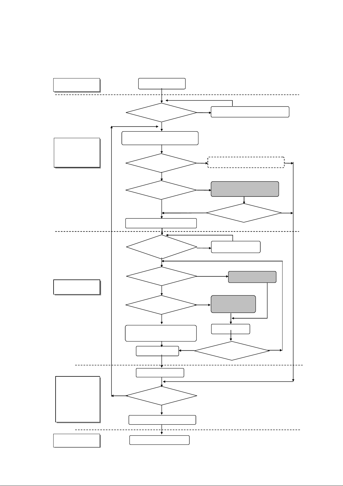
4 PROBLEM ANALYSIS
Y
Y
YNY
YYY
Y
4.1 OUTLINE OF REPAIR FLOW
Client
Product
manufacturer
(Repair center)
Client claim
Repair product
and Claim contents match
Product block/PDP module block
Locating cause of problem
Is PDP module block
Defective ?
Is the Panel defective ?
PDP module sent to factory
Repair product and
claim contents match
Recheck the problem description
N
Product problem analysis/Repair
PC board replacement/Parts
N
N
replacement
Operation normal ?
Recheck problem
description
Y
Repair center
Product
manufacturer
(Repair center)
Client
Is the panel faulty?
PC board
unacceptable (NG) ?
Processing to prevent
recurrence
Packing/Shipment
Installation in product
N
Product runs normally ?
Return of repaired product
End of repair
Panel replacement/IC
module replacement
N
PC board
replacement/Parts
replacement
N
Heat run
Operation normal ?
N
-15-
Page 20
4.2 OUTLINE OF PDP MODULE REPAIR FLOW
Receipt of returned product
(Chapter 4.3)
returned product agree with ID
Does ID of
of actual
Yes
Appearance check
Yes
Appearance unacceptable
(NG) ?
Yes
Repair of appearance
requested ?
Yes
Repair defective spots
No
No
No
Repair description and returned
product rechecked.
Perform operation test
(Chapter 4.4).
Problem recurred ?
2
Check description of
repair request.
4
No
Yes
Contents match ?
Yes
13 5
No
Problem symptom
nonrecurrence analysis mode
-16-
Page 21

1
Fault mode classification (Chapter 4.5)
Fault analysis (Chapter 4.6)
Repair of faulty spots (Chapter 5)
Replace LOGIC PC board or
panel chassis ?
No
3
Perform operation test (Chapter 4.4)
Problem repaired?
Yes
Warranty test (Running)
End of repair
Yes
Adjustment (Chapter 6)
No
Shipment
-17-
Page 22

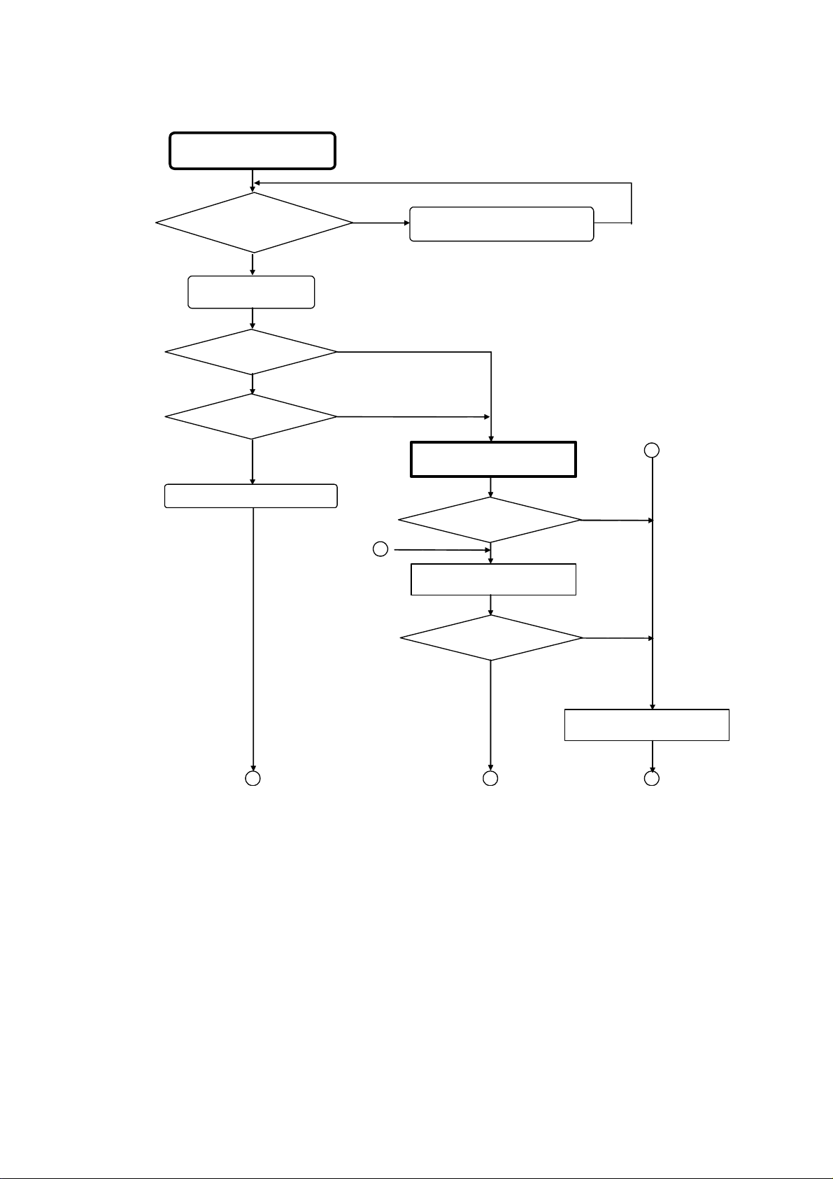
Problem symptom nonrecurrence
5
analysis mode/Shipment process mode
Implement module tapping
Problem recurs ?
No
Yes
Turn off the main power
2
Perform running test (Burn-in pattern)
No
Problem recurs ?
Yes
3
-18-
Page 23

4.3 CHECKING THE PRODUCT REQUESTED FOR REPAIR
Check the serial ID number of the product requested for repair before starting the problem
analysis and repair. Structure of serial ID number is shown below.
(1) Checking serial ID number of PDP module (14 digits)
The serial ID number of the product that is brought in for service and that of the
completed panel chassis has the structure as shown below.
The serial ID number is shown on the bar code label that is attached to the rear of the
chassis (aluminum).
N9A 4 01 001A1 01A
Version No.: 01 ~ 99
A ~ Z (excluding I and O)
Lot No.: 001 ~ 999
A ~ Z (excluding I and O)
1 ~ 3
Production week code: 01 ~ 53
Production year (low digit): 0 ~ 9
Product code: N9A- model 55 type
Module product label Serial ID label of panel chassis
* The module serial ID number and the serial ID number of the completed chassis are usually the same
when the product is brought in for repair for the first time.
(2) Checking serial ID number of constituent PC boards (12 digits)
The serial ID number of the module constituent PC boards has the following structure.
The serial ID number is shown on the bar code label that is attached to each PC board.
CP 1 01 00001 1A
Version No.: 1 ~ 9 , a~z
A ~ Z (excluding I and O)
Lot No.: 00001 ~ Z9999
Production week code: 01 ~ 53
Production year (low digit): 0 ~ 9
Product code: Different 2 digits for each board
-19-
Page 24

4.4 OPERATION TEST PROCEDURE
d
f
Five screws
Photp 4.1 Photo 4.2
(1) Prepare the test equipment.
(2) Set the PSU board (PS-jig) by five M3X8 screw on the module o
requestedfor repair. (photo4.1)
(3) Connect the cable connector from PSU board to CN9 on logic boar
and CN21 on XSUS board. (photo4.2)
(4) Set the module of requested repair to a stand.
(5) Connect between the CN1/CN2 on the logic board and the CN5/CN7
on the interface board (I/F-jig) by particular cable. (photo4.3)
(6) Turn on the AC power to the interface board (I/F-jig).
(7) Select the signal used when a problem occurs, or full white pattern.
(8) Turn on the PDP go switch on the interface board (I/F-jig). (Then, the main
power of the module is turned on.)
Check Fault Symptom
CN21
X-SUS
CN9
LOGIC
-20-
Page 25

F
Photo 4.3
< State of initialization>
CN7 CN5
CN2
CN1
PDPgo switch
ON
OF
Select switch of Display size,
Synchronous, and Clock signal
-21-
Page 26

4.5 FAULT SYMPTOM
NO Fault
contents
Entire screen
1 After momentarily going on, the
does not light.
2
3 Single vertical line (of different
Vertical line
4 Single vertical line (of different
screen becomes black
immediately or after a few
seconds. (Main power is turned
off.)
Screen lights dimly even on the
back screen.
color) start point at center of
screen
color) start point exclude at
center of screen
Fault status Suspected
5
Single full vertical line (of different
color)
Analysis
fault location
X-SUS,Y-SUS
PSU, Panel
chassis, Logic
ABUSL or R
Logic Replace
procedure
and
measure
Refer to
Chapter
4.6.1
Logic
board
Panel chassis
Logic, ABUS,
ADM
Refer to
Chapter
4.6.2
Panel chassis Replace
Panel
chassis
Logic Replace
Logic
board
6
Vertical bar Bar width of 1/33 of horizontal
7 Abnormal display at bar width of
8 Abnormal display at bar width of
9 Abnormal display at bar width of
10 Abnormal display at bar width of
11 Abnormal display at upper side
size or abnormal display in
multiples of 1/33.
1/11 of horizontal size or
multiples of 1/11
.
1/11 of horizontal size (Vertical
bar of different color)
2/11 of horizontal size (Vertical
bar of different color)
2/11 of horizontal size (Vertical
bar of different color)
or lower side of horizontal size
(Vertical bar of different color)
Panel chassis
(ADM)
Panel chassis
ABUS
Connection of
above boards.
Connection of
ADM,
ABUS
Connection of
ABUS
Connection of
ABUS
Connection of
ABUS and
Logic or
X-SUS and
ABUS
Refer to
Chapter
4.6.2
Refer to
Chapter
4.6.2
-22-
Page 27

NO Fault contents Fault status Suspected
A
fault location
12 One hall horizontal line
Horizontal line
does’nt light or one horizontal
line does not light from the
effective scan area.
13
Horizontal bar
14 Abnormal display (or no
15
16 Image sticking Fixed display contents are
17 Stains Oval-shaped points having
18 Twinkle The entire screen
19 Flicker The entire screen flickers
20 Luminance is
abnomal
21 Chrominance is
abnomal
22 Synchronization
is disturbed
Every other line does’nt light
on entire screen.
display) at bar width of 1/12 of
vertical size or multiples of
1/12
Abnormal display (or no
display) at bar width of 1/2 of
vertical size or multiples of
1/2
always displayed.
abnormal luminance are
scattered in the upper or
lower part of screen
momentarily becomes
brighter or darker
continuously
Screen is too dark or too
bright (out of specifications)
Colors cannot be displayed
correctly
Panel chassis
(SDM)
X-SUS
Y-SUS
ABUS-D2
ABUS-D3
BCDEFG
Panel chassis
(SDM)
Panel chassis
Y-SUS
X-SUS
Connection of
board
Panel chassis Judge after
Panel chassis Judge after
Poor
connector
contact
(CN1,2)
Logic
Logic
Analysis
procedure and
measure
Replace Panel
chassis
Replace
X-SUS/Y-SUS
ABUS-D2
ABUS-D3
Replace Panel
chassis
Refer to
Chapter 4.6.3
operating test
on full white
display,
Replace Panel
chassis
operating test
on full white
display,
Replace Panel
chassis
Connector /
cable
re-connection
or cable
exchange
Replace logic
board
Replace logic
board
-23-
Page 28

NO Fault contents Fault status Suspected
fault
location
23
Picture
distorted
Logic
24
Steps of
gradarion are
skipped
Luminance linearity is
poor
Logic
25
Abnormal
sound
26
External
communication
Adjustment and γ
cannrot be changed
PSU
X-SUS
Y- SU S
Panel
Logic
is abnormal
27
No light after
abnormal
display
Brightly and random
display, and it becomes
no light afterwards.
Y-SUS
Analysis
procedure and
measure
Replace logic
board
Replace logic
board
Abnormal
locations are
exchanged
Replace logic
board
Replace Y-SUS
board
-24-
Page 29

4.6 PROBLEM ANALYSIS PROCEDURE
p
(
p
4.6.1. "The entire screen does not light (Main power is turned off)” Problem analysis procedure
The entire screen does not light.
(Main power is turned off.)
PC for analysis
Connected?
N
Y
Analysis using PC
Chapter 4.7
Remove CN9 (LOGIC)
Turn on AC power.
PSU board
r2 (3.3V)
V
N
PSU board is
defective.
Turn off AC power.
Connect CN 9 (LOGIC).
Turn on AC power
Y
STANDBY power
supply has defect
Remove the following power connectors
PSU board
r2 (3.3V) exists?
V
Y
Turn off the AC power.
(4 locations):
CN 21 (X-SUS)
CN 31 (Y-SUS)
CN 4-5 (ABUS-U4)
CN 24
ABUS-D4)
N
LOGIC board is
defective.
STANDBY power supply
(MPU power supply) system
has short-circuited.
Turn off the AC
power.
End of analysis
(1)
-25-
Page 30

A
p
(1)
CN21
(3)(4) : Vcc
(5)(6)(7)’: GND
(8)(9)(10) : Vs
X-SUS board
CN21 (3)-(5) pins or
CN21 (7)-(8) pins
are shorted.
N
Y
X-SUS board is
defective.
Switching circuit (power supply)
has short-circuit.
CN31
(2)(3)(4): Vs
(7) : Vcc
(6)(8) : GND
CNU4-5
(1)(2): Va
(4)(5) : Vcc
(6)(7): GND
Y-SUS board
CN31 (4)-(6) pins or
CN31 (7)-(8) pins
are shorted.
N
ABUSU4 board
CNU4-5 (1)-(7) or
CNU4-5 (5)-(7) short
N
Y
Remove SDM from the
following (2) connectors.*
CN 32
CN 33
Y-SUS board
CN31 (4)-(6) pins or
CN32 (7)-(8) pins
are shorted.
Y
Y
Disconnect the following (3)
connectors.*
CNU2-4(ABUS-U2)
CNU3-5(ABUS-U3)
CNU3-10(ABUS-U3)
* Refer to Chapter 5.3 for
SDM removal procedure.
SDM is
defective
(Panel chassis
is defective.)
SDM chip/Flexible shorted
Y-SUS board is
defective.
Switching circuit
(power supply) has
CNU4-5
1
in
(2)
Each ABUS-U* board
CNU1-4(1)-(7) or (5)-(7)
CNU2-7(1)-(7) or (5)-(7)
CNU3-10(1)-(7) or 5)-(7)
CNU4-3(1)-(7) or (5)-(7)
short
Y
Power supply circuit has short-circuited.
N
ADM is defective
(Panel chassis is
defective.)
DM chip/Flexible shorted
ABUS-U* board
is defective.
End of analysis
-26-
Page 31

p
(2)
CND4-5
(1)(2): Va
(4)(5): Vcc
(6)(7): GND
Re-connect the following (4)
Power supply connectors.
ABUSD4 board
CND4-5 (1)-(7) or
CND4-5 (5)-(7)
short.
N
CN21 (X-SUS)
CN31 (Y-SUS)
CNU4-5 (ABUS-U4)
CN24 (ABUS-D4)
Y
Disconnect the following (3)
connectors.*
CND2-4(ABUS-D2)
CND3-5(ABUS-D3)
CND3-10(ABUS-D3)
Each ABUS-D* board
CND2-4 (1)-(7) or (5)-(7)
CND2-9 (1)-(7) or (5)-(7)
CND3-12 (1)-(7) or (5)-(7)
CND4-3 (1)-(7) or (5)-(7)
short.
Y
Power supply circuit has short-circuited.
CND4-5
N
ADM is defective
(Panel chassis is
defective.)
ADM chip/Flexible shorted
ABUS-D* board is
defective.
1
in
End of analysis
Turn on AC power.
Turn on the PDP go switch on the
interface board jig.
PSU board
Vcc (5V) exist?
Y
(3)
N
LOGIC board is
defective.
Control logic power system has short-circuited.
Turn off the AC
power.
End of analysis
-27-
Page 32

(
(3)
Turn on AC power.
PSU board
Va (63V) exist?
N
Turn off the AC power.
Disconnect
CNU4-5(ABUSU4).
Turn on AC power.
PSU board
Va (63V) exist?
N
Turn off the AC power.
Disconnect
CND4-5(ABUSD4).
Turn on AC power.
Y
ADM is defective.
ADM chip has abnormality.
Y
ABUSU1-4 boards
are defective.
Power supply line has abnormality.
Ex. capacitor)
PSU board
Va (63V) exist?
N
PSU board
Vs (85V) exist?
N
Turn off the AC power.
(4)
Y
ABUSD1-4 boards
are defective.
Turn off the AC power.
Power supply line has abnormality.
(Ex. capacitor)
End of analysis
Y
PSU board is
defective (Vs).
Turn off the AC power.
End of analysis
-28-
Page 33

A
(4)
Disconnect between
SDM and Y-SUS
Measure of SDM power line
resistor (A1-A2, B1-B2,
C1-C2, D1-D2)
Does SDM power
supply line short?
N
Y
SDM is defective.
(Panel chassis is
defective.)
SDM chip operation is abnormal.
Turn on AC power.
Y
Turn off the
AC power.
N
PSU board
Vs (85V) and Vcc
(5V) exist?
(5)
Turn off the AC
power.
1
A2
B1
B2
C1
C2
D1
D2
-29-
Page 34

X
X
A
A
A
A
(5)
Disconnect between
XBB and X-SUS
Measure of XBB line resistor
(A1-B1, B1-A2, A2-B2, B2-A3,
A3-B3, B3-A4, A4-B4)
Does XBB line
short?
Y-SUS board is defective.
-SUS board is defective.
XBB is defective. (Panel
chassis is defective.)
-SUS board is defective.
Turn off the AC power.
End of analysis
1
B1
2
B2
3
B3
4
B4
-30-
Page 35

4.6.2 "Vertical line/Vertical bar" Problem analysis procedure
A
j
Vertical line/Vertical bar
LOGIC ~ ABUS board signal
cable has abnormal appearance?
N
Y
Signal cable is
defective.
ADM flexible has abnormal
appearance?
N
Turn on the power.
One vertical line?
N
Y
Y
Tap lightly on ADM flexible
heat-melted junction.
ny changes
phenomena?
N
ADM is defective.
(Panel chassis is
defective.)
Y
Heat-melted
unction is defective
(Panel chassis is
defective.)
End of analysis
Turn off the
power.
Panel address has open
circuit or ADM IC chip is
(Panel chassis is defective.)
(1)
defective.
End of analysis
-31-
Page 36

N
(1)
Bar of 1/2 width on
the upside does
not light?
Bar of 1/2 width on
the downside does
not light?
N
N
Y
Voltage exists at
ABUSU4 board
CN U4-5.
N
Turn off the power.
Disconnect CNU4-5 on the
ABUSU4 board.
Turn on the power.
Voltage exists
at PSU Side?
N
Y
Voltage exists at
ABUSD4 board
CND4-5?
N
Y
Y
Y
LOGIC board is
defective.
ABUSU* board is
defective.
PSU cable is
defective. Connector
has poor connection
(LOGIC board is
defective.)
LOGIC board is
defective.
(2)
Turn off the power.
Disconnect CND4-5 on the
ABUSD4 board.
Turn on the power.
Voltage exists
at PSU Side?
N
-32-
Y
ABUSD board is
defective.
PSU cable is defective. Connector
has poor connection.
(PSU board is defective.)
Turn off the power.
End of analysis
Page 37

p
(2)
Vertical line of
different color
does appear?
Y
N
Exists on half
upside?
Y
N
Turn off the power.
Replace ABUSU board
(Backup part).
Turn on the main power.
Normal?
Y
ABUSU board is
defective.
N
Replace LOGIC board (Backup part)
Turn off the power.
Turn on the power.
Y
Normal?
LOGIC board is
defective.
N
Turn off the power.
Replace signal cable between
LOGIC and ABUSU.
Turn on the
Normal?
ower.
Y
N
Signal cable is
defective.
ADM is defective.
(Panel chassis is
defective.)
Turn off the power.
End of analysis
(3)
(4)
-33-
Page 38

(3)
(4)
Replace ABUSD board (Backup part).
Turn off the power.
Turn on the power.
Normal?
Y
ABUSD board is
defective.
N
Replace LOGIC board (Backup part).
Turn off the power.
Turn on the power.
Normal?
N
Y
LOGIC board is
defective.
Replace signal cables between LOGIC
Turn off the power.
and ABUS.
Turn on the power.
Panel is defective.
(Panel chassis is
defective.)
Normal?
N
Y
Signal cable is
defective.
ADM is defective.
(Panel chassis is
defective.)
Turn off the main power.
End of analysis
-34-
Page 39

4.6.3 "Horizontal bar" Problem analysis procedure
Replace Y-SUS board (Backup part).
Horizontal bar
Turn off the power.
Turn on the power.
Normal?
Replace Y-SUS board (Defective product).
Replace X-SUS board (Backup part)
Turn off the power.
Turn on the power.
N
Y
Y-SUS board is
defective.
Normal?
N
Y
X-SUS board is
defective.
Replace X-SUS board (Defective product).
Replace ABUS-D2 and D3 board (Backup part)
Turn off the power.
Turn on the power.
Normal?
N
Y
ABUS-D2 and D3 board
are defective.
Panel chassis is
defective.
Turn off the power.
End of analysis
-35-
Page 40

4.7 PROBLEM ANALYSIS USING A PERSONAL COMPUTER
4.7.1 Connecting a computer
(1) Set the module in accordance with Chapter 4.4.
(2) Connect the RS-232C terminal of the computer to the RS-232C terminal of the interface
board.
(3) Turn on the main power to the interface board. (Red LED goes on.)
POWER indicator (red LED)
4.7.2 Preparing a computer
(1) Turn on the main power to the computer.
(2) Set the PDPgo switch on the interface board to ON and turn on the main power to the
module.
(3) For computer running MS-DOS:
C: \ >FHPP1<ENTER>
For computer running WINDOWS:
Start menu → Run → FHPP1<ENTER>
(4) The following menu screen appears.
Main menu
*1: Use COM1: for the computer's communication port.
*2: Set the communication setup as follows.
Speed: 9600 bps
Data: 7 bits
Parity: none
In Windows, restart the computer after setting the communication setup.
*3: If the program starts up while the module standby power is not yet turned on, the menu
screen will not be displayed.
Stop bit: 1 bit
-36-
Page 41

4.7.3 Problem Analysis Procedure
(1) Select the problem analysis menu from the main menu using the ↑key or ↓key and press
<ENTER> key to start the program.
Main menu
(2) Check the error code (hexadecimal number) from the Latest error code read-out menu and
locate the faulty position from the following table.
Problem analysis menu
The state of the module
The latest error code
A past error code is shown in
new the order.
All error code is cleared to 0.
Example of displaying breakdown analysis
(3) Confirm the latest error code, and then the faulty point is specified from the Error code table.
(4) Select RETURN using the ↑key or ↓key and press <ENTER> key to start the program, then
the screen returns to the menu screen.
* When EXIT is selected, the screen returns to the WINDOWS or DOS screen.
-37-
Page 42

Error code table
Detect
ERR
code
position
(board)
Contents
(In the order of higher probability of defect)
(1) (2) (3) (4) (5) (6) (7)
00 LOGIC STANDBY power is stopped PSU PSU temperature
LOGIC
02 ROM data of waveform is abnormal LOGIC
04 3.3V power voltage has dropped LOGIC PSU
06 3.3V power startup is faulty X-SUS Y-SUS
08 1V power voltage has dropped LOGIC PSU
0A 1V power startup is faulty X-SUS Y-SUS ADM1-22 PSU ABUS LOGIC
18 Internal I2C_SCL1_LOW level LOGIC
19 Internal I2C_ACK does not respond LOGIC
1C EEPROM initial setting is defective LOGIC
1D EEPROM write-down is defective LOGIC
1E EEPROM user initial setting is
LOGIC
defective
1F
EEPROM factory setting reading is
LOGIC
defective
X-SUS
24 Vex power voltage has decreased X-SUS LOGIC
25 Vex power voltage is excessive X-SUS
26 Vex power startup is faulty. X-SUS LOGIC
28 Vx power voltage has dropped X-SUS LOGIC
29 Vx power voltage is excessive X-SUS
2A Vx power startup is faulty. X-SUS LOGIC
39 Vs power current is excessive
X-SUS Panel LOGIC
(during operation)
3B Vs power current is excessive
X-SUS Panel LOGIC
(during startup)
3C Vq power voltage has dropped X-SUS
3D Vq power voltage is excessive X-SUS
3E
44 Vey power voltage has dropped Y-SUS LOGIC
Y-SUS
Vq power startup is faulty. X-SUS
45 Vey power voltage is excessive Y-SUS
46 Vey power startup is faulty. Y-SUS LOGIC
48 Vu power voltage has dropped Y-SUS
49 Vu power voltage is excessive Y-SUS
4A Vu power startup is faulty. Y-SUS
59 Vs power current is excessive
Y-SUS Panel LOGIC
(during operation)
5B Vs power current is excessive
Y-SUS Panel LOGIC
(during startup)
5D
X-SUS
61 Vs power voltage is excessive PSU X-SUS LOGIC
Y-SUS
62 Vs power startup is faulty. X-SUS Y-SUS PSU LOGIC
64 Ve power voltage has dropped LOGIC X-SUS Y-SUS
SDM current is excessive SDM Y-SUS Panel LOGIC
65 Ve power voltage is excessive X-SUS Y-SUS
66 Ve power startup is faulty. LOGIC X-SUS Y-SUS
68 Vw power voltage has dropped Y-SUS X-SUS LOGIC
69 Vw power voltage is excessive X-SUS
6A
ABUS
81 Va power voltage is excessive PSU X-SUS LOGIC
82 Va power startup is faulty.
99 Va power current is excessive
9B
Vw power startup is faulty. Y-SUS X-SUS LOGIC
(during operation)
Va power current is excessive
(during startup)
ADMU1-U11
ADND1-D11
ADMU1-U11
ADND1-D11
ADMU1-U11
ADND1-D11
PSU X-SUS LOGIC ABUS
ABUS X-SUS PSU LOGIC
ABUS X-SUS PSU LOGIC
Suspected faulty board
ADMU1-U11
ADND1-D11
PSU
ABUSU1-U4
ABUSD1-D4
Remarks
has probably
increased
LOGIC
-38-
Page 43

Detect
ERR
position
code
(board)
9D Va power current is excessive (during
A5 ADM-D1 ADM-D1 has abnormal heat generation. ADM-D1 PSU LOGIC
A7 ADM-U1 ADM-U1 has abnormal heat generation. ADM-U1 PSU LOGIC
A9 ADM-D2 ADM-D2 has abnormal heat generation. ADM-D2 PSU LOGIC
AB ADM-U2 ADM-U2 has abnormal heat generation. ADM-U2 PSU LOGIC
AD ADM-D3 ADM-D3 has abnormal heat generation. ADM-D3 PSU LOGIC
AF ADM-U3 ADM-U3 has abnormal heat generation. ADM-U3 PSU LOGIC
B1 ADM-U4 ADM-U4 has abnormal heat generation. ADM-U4 PSU LOGIC
B3 ADM-D4 ADM-D4 has abnormal heat generation. ADM-D4 PSU LOGIC
B5 ADM-U5 ADM-U5 has abnormal heat generation. ADM-U5 PSU LOGIC
B7 ADM-D5 ADM-D5 has abnormal heat generation. ADM-D5 PSU LOGIC
B9 ADM-U6 ADM-U6 has abnormal heat generation. ADM-U6 PSU LOGIC
BB ADM-D6 ADM-D6 has abnormal heat generation. ADM-D6 PSU LOGIC
BD ADM-U7 ADM-U7 has abnormal heat generation. ADM-U7 PSU LOGIC
BF ADM-D7 ADM-D7 has abnormal heat generation. ADM-D7 PSU LOGIC
C5 ADM-U8 ADM-U8has abnormal heat generation. ADM-U8 PSU LOGIC
C7 ADM-D8 ADM-D8 has abnormal heat generation. ADM-D8 PSU LOGIC
C9 ADM-U9 ADM-U9has abnormal heat generation. ADM-U9 PSU LOGIC
CB ADM-D9 ADM-D9 has abnormal heat generation. ADM-D9 PSU LOGIC
CD ADM-U10 ADM-U10has abnormal heat
CF ADM-D10 ADM-D10 has abnormal heat
D1 ADM-U11 ADM-U11has abnormal heat
D3 ADM-D11 ADM-D11 has abnormal heat
E2 LOGIC 5V power startup is faulty. X-SUS Y-SUS PANEL PSU ABUS LOGIC
FC PSU Detection error of Vs and Va voltage. PSU LOGIC
operation)
generation.
generation.
generation.
generation.
Contents
Contents
(In the order of higher probability of defect)
(1) (2) (3) (4) (5) (6) (7)
ADM1-8 ABUS PSU LOGIC Excess current is
ADM-U10 PSU LOGIC
ADM-D10 PSU LOGIC
ADM-U11 PSU LOGIC
ADM-D11 PSU LOGIC
Suspected faulty board
Remarks
detected in ACCC
operation.
It can possibly
occur depending
on screen display.
-39-
Page 44

5 DISASSEMBLING AND REASSEMBLING
⑬
③
④
⑤
⑥⑦⑧
⑫① ⑭⑮⑯ ⑱
⑰
⑲
Unless otherwise specified, use the torque screwdriver for screw tightening, following the
tightening torques.
Screw size Tightening torque
M 3 0.69±0.049Nm (7±0.5kg·cm)
M 4 1.18±0.098Nm (12±1.0kg·cm)
5.1 Exploded View
②
⑲
⑲
⑨
⑩
⑲
⑪
⑲
⑲
-40-
Page 45

5.2 X-SUS Circuit Board Removal/Installation Procedure
(4)
When removing the circuit board after the main power is turned on/off, wait for at
Note
CN22
(5)
least four minutes before starting to remove the circuit board.
If the circuit board removal is started immediately after turning off the main power, it
can result in electric shock or damage to the circuit due to residual electric charge.
Remove the circuit board following the steps below. To install the circuit board, reverse the removal
procedure.
(1) Remove the fixing screws (M3x8) fixing XBB at 4 locations.
(2) Pull out the XBB board horizontally and disconnect the connectors (CN26, CN27).
(3) Release the lock of the FPC connector (CN20) and disconnect the signal cable.
(4) Disconnect the cables from the VH connectors (CN22, CN23, CN24).
(5) Remove the fixing screws (M3x8) fixing XSUS at 7 locations.
(6) Release the space holder (rod) at the 3 locations.
(7) Remove the X-SUS board.
(1)
(4)CN23
(6)
(2)CN26
(5)
Pull out
(5)
(5)
(5)
(5)
(3)CN20
(5)
Pull out
(6)
Note
(4)CN24
*
On handling the FPC connector
To release the lock, release it by gently flipping it with the nail of the
thumb or forefinger. Never pinch the lock lever with fingers or hook
on it (especially with a fingernail). Doing so might damage the lock
lever.
(1)
(1)
(2)CN27
(6)
(1)
-41-
Page 46

p
y
③
Note
Pick up and release upper the lock of space
holder (rod). Moreover, confirm the lock surel
combines intuition when you install the board.
Space holder (rod)
Pick up Pick u
PCB
-42-
Page 47

5.3 Y-SUS Circuit Board Removal/Installation Procedure
3
When removing the circuit board after the main power is turned on/off, wait for at
Note
(1)
(1)
least four minutes before starting to remove the circuit board.
If the circuit board removal is started immediately after turning off the main power, it
can result in electric shock or damage to the circuit due to residual electric charge.
Remove the circuit board following the steps below. To install the circuit board, reverse the removal
procedure.
(1) Remove the fixing screws (M3x8) fixing SDM at 6 locations.
(2) Pull out the SDM board horizontally and disconnect the connectors (CN32, CN33).
(3) Release the lock of the FPC connector (CN30) and disconnect the signal cable.
(4) Disconnect the power supply connectors (CN31).
(5) Remove the fixing screws (M3x8) fixing YSUS at 6 locations.
(6) Release the space holder (rod) at the 4 locations.
(7) Remove the Y-SUS board.
(6)
(4)CN31
(2)CN32
(5)
(1)
Pull out
(5)
(1)
(5)
Pull out
(2)CN3
(1)
(6)
(1)
Note
* On handling the FPC connector
To release the lock, release it by gently flipping it with the nail of the
thumb or forefinger. Never pinch the lock lever with fingers or hook
on it (especially with a fingernail). Doing so might damage the lock
lever.
(3)CN30
(6)
(5)
(5)
(5)
(6)
-43-
Page 48

y
p
④
Note
Pick up and release upper the lock of space
holder (rod). Moreover, confirm the lock surel
combines intuition when you install the board.
Space holder (rod)
Pick up Pick u
PCB
-44-
Page 49

5.4 ABUS-U1 Circuit Board Removal/Installation Procedure
3
When removing the circuit board after the main power is turned on/off, wait for at
Note
least four minutes before starting to remove the circuit board.
If the circuit board removal is started immediately after turning off the main power, it
can result in electric shock or damage to the circuit due to residual electric charge.
Remove the circuit board following the steps below. To install the circuit board, reverse the removal
procedure.
(1) Release the lock of CNU1-3 and then reconnect the signal cable (FPC).
(2) Release the lock of CNU1-1, CNU1-2 by lifting the lock and then reconnect flexible cable of ADM.
(3) Release the power supply connector CNU2-4 on the ABUS-U2 board.
(4) Remove the fixing screws (M3x8) fixing ADM at 4 locations.
(5) Remove the fixing screws (M3x8) fixing ABUS-U1 at 1 location.
(6) Release the space holder (rod) at the 1 location.
(7) Remove the ABUS-U1 board.
(2)CNU1-1
(2)CNU1-2
(3)CNU2-4
(4)
(4)
(4)
(6)
(2)CN3
(5)
(1)CNU1-3
Note
(4)
* On handling the FPC connector
To release the lock, release it by gently flipping it with the nail of the
thumb or forefinger. Never pinch the lock lever with fingers or hook
on it (especially with a fingernail). Doing so might damage the lock
lever.
-45-
Page 50

y
p
⑤
Note
Pick up and release upper the lock of space
holder (rod). Moreover, confirm the lock surel
combines intuition when you install the board.
Pick up Pick u
Space holder (rod)
PCB
-46-
Page 51

5.5 ABUS-U2 Circuit Board Removal/Installation Procedure
3
When removing the circuit board after the main power is turned on/off, wait for at
Note
least four minutes before starting to remove the circuit board.
If the circuit board removal is started immediately after turning off the main power, it
can result in electric shock or damage to the circuit due to residual electric charge.
Remove the circuit board following the steps below. To install the circuit board, reverse the removal
procedure.
(1) Release the lock of CNU2-5, CNU2-6 and then reconnect the signal cable (FPC).
(2) Release the lock of CNU2-1, CNU2-2, CNU2-3
(3) Release the CNU2-4 and power supply connector CNU3-5 on the ABUS-U3 board.
(4) Remove the fixing screws (M3x8) fixing ADM at 6 locations.
(5) Remove the fixing screws (M3x8) fixing ABUS-U2 at 2 locations.
(6) Release the space holder (rod) at the 1 location.
(7) Remove the ABUS-U2 board.
(2)CNU2-3
(2)CNU2-1
(2)CNU2-2
by lifting the lock and then reconnect flexible cable of ADM.
(3)CNU3-5
(3)CNU2-4
(4)
(4)
(4)
(5)
(2)CN3
(1)CNU2-5
Note
* On handling the FPC connector
To release the lock, release it by gently flipping it with the nail of the
thumb or forefinger. Never pinch the lock lever with fingers or hook
on it (especially with a fingernail). Doing so might damage the lock
lever.
(4)
(4)
(6)
(1)CNU2-6
(4)
(5)
-47-
Page 52

y
p
⑥
Note
Pick up and release upper the lock of space
holder (rod). Moreover, confirm the lock surel
combines intuition when you install the board.
Space holder (rod)
Pick up Pick u
PCB
-48-
Page 53

5.6 ABUS-U3 Circuit Board Removal/Installation Procedure
When removing the circuit board after the main power is turned on/off, wait for at
Note
(2)CNU3-4
least four minutes before starting to remove the circuit board.
If the circuit board removal is started immediately after turning off the main power, it
can result in electric shock or damage to the circuit due to residual electric charge.
Remove the circuit board following the steps below. To install the circuit board, reverse the removal
procedure.
(1) Release the lock of CNU3-6, CNU3-7, CNU3-8, CNU3-9 and then reconnect the signal cable (FPC).
(2) Release the lock of CNU3-1, CNU3-2, CNU3-3, CNU3-4
of ADM.
(3) Release the power supply connector CNU3-5, CNU3-10 on the ABUS-U3 board.
(4) Remove the fixing screws (M3x8) fixing ADM at 8 locations.
(5) Remove the fixing screws (M3x8) fixing ABUS-U3 at 2 locations.
(6) Release the space holder (rod) at the 1 location.
(7) Remove the ABUS-U3 board.
by lifting the lock and then reconnect flexible cable
(2)CNU3-3
(2)CNU3-2
(2)CNU3-1
(4)
(4)
(4)
(4)
(6)
(4)
(4)
(4)
(5)
(5)
(1)CNU3-6(3)CNU3-5
Note
* On handling the FPC connector
To release the lock, release it by gently flipping it with the nail of the
thumb or forefinger. Never pinch the lock lever with fingers or hook
on it (especially with a fingernail). Doing so might damage the lock
lever.
(4)
(1)CNU3-10
(1)CNU3-9
(1)CNU3-8(1)CNU3-7
-49-
Page 54

y
p
⑦
Note
Pick up Pick u
Pick up and release upper the lock of space
holder (rod). Moreover, confirm the lock surel
combines intuition when you install the board.
Space holder (rod)
PCB
-50-
Page 55

5.7 ABUS-U4 Circuit Board Removal/Installation Procedure
When removing the circuit board after the main power is turned on/off, wait for at
Note
(3)CNU3-10
least four minutes before starting to remove the circuit board.
If the circuit board removal is started immediately after turning off the main power, it
can result in electric shock or damage to the circuit due to residual electric charge.
Remove the circuit board following the steps below. To install the circuit board, reverse the removal
procedure.
(1) Release the lock of CNU4-4 and then reconnect the signal cable (FPC).
(2) Release the lock of CNU4-1, CNU4-2
(3) Release the CNU4-5 and power supply connector CNU3-10 on the ABUS-U3 board.
(4) Remove the fixing screws (M3x8) fixing ADM at 8 locations.
(5) Remove the fixing screws (M3x8) fixing ABUS-U3 at 2 locations.
(6) Release the space holder (rod) at the 1 location.
(7) Remove the ABUS-U3 board.
by lifting the lock and then reconnect flexible cable of ADM.
(4)
(2)CNU4-2
(2)CNU4-1
(4)
(5)
(4)
(5)
(6)
(1)CNU4-4 (3)CNU4-5
Note
* On handling the FPC connector
To release the lock, release it by gently flipping it with the nail of the
thumb or forefinger. Never pinch the lock lever with fingers or hook
on it (especially with a fingernail). Doing so might damage the lock
lever.
(4)
-51-
Page 56

e
y
p
⑧
Note
Pick up and release upper the lock of spac
holder (rod). Moreover, confirm the lock surel
combines intuition when you install the board.
Space holder (rod)
-52-
Pick up Pick u
PCB
Page 57

5.8 ABUS-D1 Circuit Board Removal/Installation Procedure
When removing the circuit board after the main power is turned on/off, wait for at
Note
least four minutes before starting to remove the circuit board.
If the circuit board removal is started immediately after turning off the main power, it
can result in electric shock or damage to the circuit due to residual electric charge.
Remove the circuit board following the steps below. To install the circuit board, reverse the removal
procedure.
(1) Release the lock of CND1-3 and then reconnect the signal cable (FPC).
(2) Release the lock of CND1-1, CND1-2 by lifting the lock and then reconnect flexible cable of ADM.
(3) Release the power supply connector CND2-4 on the ABUS-U3 board.
(4) Remove the fixing screws (M3x8) fixing ADM at 4 locations.
(5) Remove the fixing screws (M3x8) fixing ABUS-D1 at 1 location.
(6) Release the space holder (rod) at the 1 location.
(7) Remove the ABUS-D1 board.
(1)CND1-3
(5)
(6)
(4)
(4)
(4)
(4)
(2)CND1-1 (2)CND1-2
Note
* On handling the FPC connector
To release the lock, release it by gently flipping it with the nail of the
thumb or forefinger. Never pinch the lock lever with fingers or hook
on it (especially with a fingernail). Doing so might damage the lock
lever.
(3)CND2-4
-53-
Page 58

⑨
e
y
p
Note
Pick up and release upper the lock of spac
holder (rod). Moreover, confirm the lock surel
combines intuition when you install the board.
Space holder (rod)
Pick up Pick u
PCB
-54-
Page 59

5.9 ABUS-D2 Circuit Board Removal/Installation Procedure
When removing the circuit board after the main power is turned on/off, wait for at
Note
(1)CND2-6 (1)CND2-7
least four minutes before starting to remove the circuit board.
If the circuit board removal is started immediately after turning off the main power, it
can result in electric shock or damage to the circuit due to residual electric charge.
Remove the circuit board following the steps below. To install the circuit board, reverse the removal
procedure.
(1) Release the lock of CND2-5, CND2-6, CND2-7, CND2-8 and then reconnect the signal cable (FPC).
(2) Release the lock of CND2-1, CND2-2, CND2-3
(3) Release the power supply connector CND2-4 on the ABUS-D2 board and CND3-5 on the ABUS-D3 board.
(4) Remove the fixing screws (M3x8) fixing ADM at 6 locations.
(5) Remove the fixing screws (M3x8) fixing ABUS-D2 at 2 locations.
(6) Release the space holder (rod) at the 2 locations.
(7) Remove the ABUS-D2 board.
by lifting the lock and then reconnect flexible cable of ADM.
(1)CND2-8
(1)CND2-5
(3)CND2-4
(2)CND2-3
Note
(5)
(4)
(5)
(4)
(4)
(6)
(4)
(4)
(6)
(4)
(2)CND2-2 (2)CND2-1
(3)CND2-9
* On handling the FPC connector
To release the lock, release it by gently flipping it with the nail of the
thumb or forefinger. Never pinch the lock lever with fingers or hook
on it (especially with a fingernail). Doing so might damage the lock
lever.
-55-
Page 60

⑩
p
e
y
Note
Pick up and release upper the lock of spac
holder (rod). Moreover, confirm the lock surel
combines intuition when you install the board.
Space holder (rod)
Pick up Pick u
PCB
-56-
Page 61

5.10 ABUS-D3 Circuit Board Removal/Installation Procedure
When removing the circuit board after the main power is turned on/off, wait for at
Note
least four minutes before starting to remove the circuit board.
If the circuit board removal is started immediately after turning off the main power, it
can result in electric shock or damage to the circuit due to residual electric charge.
Remove the circuit board following the steps below. To install the circuit board, reverse the removal
procedure.
(1) Release the lock of CND3-6, CND3-7, CND3-8, CND3-9, CND3-10, CND3-11 and then reconnect the signal
cable (FPC).
(2) Release the lock of CND3-1, CND3-2, CND3-3, CND3-4
of ADM.
(3) Release the power supply connector CND3-4,CND 3-12 .
(4) Remove the fixing screws (M3x8) fixing ADM at 8 locations.
(5) Remove the fixing screws (M3x8) fixing ABUS-D3 at 2 locations.
(6) Release the space holder (rod) at the 2 locations.
(7) Remove the ABUS-D3 board.
by lifting the lock and then reconnect flexible cable
(1)CND3-9 (1)CND3-8
(1)CND3-7
(1)CND3-6
(3)CND3-5
(4)
Note
(5)
(4)
(4)
(6)
(6)
(4)
(4)
(1)CND3-10
(5)
(1)CND3-11
(3)CND3-12
(4)
(4)
(4)
(2)CND3-2 (2)CND3-3 (2)CND3-4
(2)CND3-1
* On handling the FPC connector
To release the lock, release it by gently flipping it with the nail of the
thumb or forefinger. Never pinch the lock lever with fingers or hook
on it (especially with a fingernail). Doing so might damage the lock
lever.
-57-
Page 62

⑪
e
y
p
Note
Pick up and release upper the lock of spac
holder (rod). Moreover, confirm the lock surel
combines intuition when you install the board.
Space holder (rod)
Pick up Pick u
PCB
-58-
Page 63

5.11 ABUS-D4 Circuit Board Removal/Installation Procedure
When removing the circuit board after the main power is turned on/off, wait for at
Note
least four minutes before starting to remove the circuit board.
If the circuit board removal is started immediately after turning off the main power, it
can result in electric shock or damage to the circuit due to residual electric charge.
Remove the circuit board following the steps below. To install the circuit board, reverse the removal
procedure.
(1) Release the lock of CND4-4 and then reconnect the signal cable (FPC).
(2) Release the lock of CND4-1, CND4-2
(3) Release the CND4-5 and power supply connector CND3-12 on the ABUS-D3.
(4) Remove the fixing screws (M3x8) fixing ADM at 4 locations.
(5) Remove the fixing screws (M3x8) fixing ABUS-D4 at 2 locations.
(6) Release the space holder (rod) at the 1 location.
(7) Remove the ABUS-D4 board.
by lifting the lock and then reconnect flexible cable of ADM.
(1)CND4-4
(3)CND4-5
(5)
(4)
(3)CND3-12
Note
* On handling the FPC connector
To release the lock, release it by gently flipping it with the nail of the
thumb or forefinger. Never pinch the lock lever with fingers or hook
on it (especially with a fingernail). Doing so might damage the lock
lever.
(6)
(4)
(4)
(2)CND4-2
(5)
(4)
(2)CND4-1
-59-
Page 64

⑫
e
y
p
Note
Pick up and release upper the lock of spac
holder (rod). Moreover, confirm the lock surel
combines intuition when you install the board.
Pick up Pick u
Space holder (rod)
PCB
-60-
Page 65

5.12 LOGIC Circuit Board Removal/Installation Procedure
(1)CN6
(2)CN3
Remove the circuit board following the steps below. To install the circuit board, reverse the removal
procedure.
(1) Release the lock of CN4, CN5, CN6, CN7, and then reconnect the signal cable (FPC).
(2) Release the lock of CN3
(3) Remove the fixing screws (M3x8) fixing LOGIC at 3 locations.
(4) Release the space holder (rod) at the 2 locations.
(5) Remove the LOGIC board.
by lifting the lock and then reconnect signal cable.
(1)CN5
(3)
(3)
(3)
(1)CN4
(1)CN8
(1)CN7
Note
(4)
(4)
* On handling the FPC connector
To release the lock, release it by gently flipping it with the nail of the
thumb or forefinger. Never pinch the lock lever with fingers or hook
on it (especially with a fingernail). Doing so might damage the lock
lever.
-61-
Page 66

e
y
p
②
Note
Pick up and release upper the lock of spac
holder (rod). Moreover, confirm the lock surel
combines intuition when you install the board.
Space holder (rod)
Pick up Pick u
PCB
-62-
Page 67

5.13 Complete Panel chassis Removal / Installation Procedure
(1) Remove the board of 11 types (X-SUS, Y-SUS, ABUS-U1, U2, U3, U4, D1, D2, D3, D4, and LOGIC) that
are installed in the panel module. For the removal procedure, refer to section 5.2 to 5.7.
Note: Before removing the board of 11 types, be sure to release the three power supply cables and tweleve
FFC cables (White color).
-63-
Page 68

(2) Install the 11 tpyes boards that were removed by step (1) at panel chassis of repair part. (Refer to
t he disassembly figure shown in Section 5.1)
(3) Print the serial ID number of the product to be repaired on the product label which is prepared
separately. Attach the product label to the panel chassis above the Y-SUS board (See the
following photo.)
Product label
-64-
Page 69

(4) After the installation of the board is complete, connect the cables as shown below photo.
Fix the power supply cable at the cable clamp.
Expansion photo.
-65-
Page 70

6 OPERATION CHECK AND ADJUSTMENT METHOD
6.1 LIST OF CHECK AND ADJUSTMENT ITEMS
-
6
6
-
Adjustment item
(Major item)
Parameter
adjustment
Default setting
Adjustment item
(Minor item)
Vs voltage adjustment
Va voltage adjustment
Vw voltage adjustment
Vx voltage adjustment
Vq voltage adjustment
Vu voltage adjustment
Error history clear LOGIC board (EEPROM)
Accumulated power-on
time clear
(Name of the part)
LOGIC board(Vsvolt data)
X-SUSboard (TP:PVS)
LOGIC board(Vavolt data)
X-SUSboard (TP:PVA)
LOGIC board(Vwvolt data)
X-SUSboard (TP:PVW)
LOGIC board(Vxvolt data)
X-SUSboard (TP:PVX)
LOGIC board(Vqvolt data)
X-SUSboard (TP:PVQ)
LOGIC board(Vuvolt data)
Y-SUSboard (TP:PVU)
LOGIC board (EEPROM)
(Reference)
When PDP
panel is
replaced
〇
〇
〇
〇
〇
〇
〇 〇 〇 〇 〇 〇
〇
When X-SUS
board is
replaced
When Y-SUS
board is
replaced
When LOGIC
board is
replaced
〇
〇
〇
〇
〇
〇
When ABUS
board is
replaced
When PSU
board is
replaced
Jig/tools
Interface board,
personal computer,
Digital voltmeter
Interface board,
personal computer
{ : Check, adjustment, or setup
Page 71

s
s
n
6.2 CHECK AND ADJUSTMENT METHOD
6.2.1 Check and adjustment procedure
Check and adjustment
Y
Was LOGIC board
replaced?
Logic board data transfer (Section 6.2.5)
N
Was Panel chassi
replaced?
Normally?
Y
Burn-inmode setting (Section 6.2.4)
Heat run (Setion 6.2.4)
Abnormal
operation?
Y
Parameter adjustment (Section 6.2.2)
Operation and Performance check
N
Y
N
Was Panel chassi
replaced?
Y
Reset an accumulated power-o
time (Section 6.2.6)
N
Default setup (Error history clear) (Section 6.2.7)
End
-67-
Re-analysis to Section 4.2
Page 72

6.2.2 Parameter adjustment
List of parameter adjustment items
item Adjusment items parameter
1 Vs Voltage Vrs X-SUS
2 Va Voltage Vra X-SUS
3 Vw Voltage Vrw X-SUS
4 Vx Voltage Vrx X-SUS
5 Vq Voltage Vrq X-SUS
6 Vu Voltage Vru Y-SUS
*: Voltage setting label shows the following messages at the top left of the back of the chassis.
< LOT > XXXXXXXXXXXXXX
Vs=XXX.X V Va=XX.X V
Vw=XXX.X V Vx=XX.X V
Vq=XXX.X V Vu=XX.X V
Measurement
point
Adjustment value (conditions) Remarks
Voltage setting label indication value* ;
±1% (all black)
Voltage setting label indication value* ;
±2% (all black)
Voltage setting label indication value* ;
±2% (all black)
Voltage setting label indication value* ;
±3% (all black)
Voltage setting label indication value* ;
±3% (all black)
Voltage setting label indication value* ;
±3% (all black)
6,
1,2,
3,4,
5
-68-
Page 73

(1) From the main menu, select the voltage adjustment menu with the ↑ key or ↓ key and press the
<ENTER> key.
Main menu
Module information menu
POWER ON menu
Problem analysis menu
→Voltage adjustment menu
Accumulated power-on time menu
Logic board change menu
EXIT
(2) From the voltage adjustment menu, adjust parameters in the order starting from Vs, Va, Vw, Vx, Vq,
Vu.
Select parameter with the ↑ key or ↓ key and adjust the parameter with the → key (increment) or ←
key (decrement). The adjustment values are shown on the voltage label that is attached to the
panel chassis.
Voltage adjustment menu
→Voltage adjustment / Vs[V] = :**.**
Voltage adjustment / Va[V] = :**.**
Voltage adjustment / Vw[V] = :**.**
Voltage adjustment / Vx[V] = :**.**
Voltage adjustment / Vq[V] =- :**.**
Voltage adjustment / Vu[V] = :**.**
RETURN
EXIT
** Numbers are shown in decimal values.
Input the numeric value/dot and press the <ENTER> key and then press the <ENTER> key again
to set the adjustment value directly.
(3) Select RETURN with the ↑ key or ↓ key and press the <ENTER> key to return to the menu screen.
-69-
Page 74

W
6.2.3 Operation performance check items
(1) Environmental conditions
Temperature: Room temperature
Judgment distance: 1 meter from panel screen
Preheat run: 5 minutes with entire screen lit (white)
(2) Test patterns:
PSEL Push SW Display pattern Size Details
H 0 White screen
H 1 Cross slash Large 24 × 24
H 2 Vertical stripe Every other dot
H 3 Horizontal stripe Every other line
H 4 Color bars Vertical bar H_blk divided in 8
H 5 Gray scale Horiz. direction Every 3 dots
H 6 Color gray scale Horiz. direction Every 3 dots
H 7 Divided WINDOW 9 blocks Follow the ROM
L 0 1% WINDOW Center Follow the ROM
L 1 Cross slash Small 12 × 12
L 2 Vertical stripe Every other cell
L 3 Horizontal stripe Every 2 lines
L 4 Color bars Horizontal bar V_blk divided in 8
L 5 Gray scale Vert. direction Every 4 dots
L 6 Color gray scale Vert. direction Every 4 dots *2
L 7 Divided WINDOW 16 blocks Follow ROM *3
PDPGO SW
CPUGO S
-70-
Page 75

(3) Judgment
Item Test items Test signal Judgment criterion
1 Brightness non-uniformity White screen (W) Brightness non-uniformity in the form of stripes
must not be visible in vertical and horizontal
directions.
2 Black noise Horizontal gray scale
(Each color of R/G/B)
3 Number of defects
4 Number of extra dots
5 Number of flickering dots
The entire screen lights
(Each color of W/R/G/B)
Rank 3 or higher in the 5-step evaluation.
<Rank>
5: No noise
4: Small noise is intermittently visible
3: Noise of 1 line is not visible continuously
2: Noise occurs continuously
1: Much noise occurs continuously
Conforms to Section 1.3.2 Display quality
specifications.
However, when Delivery Specifications Sheets
are prepared for each client, the specifications
shown in the Delivery Specifications Sheet must
be met.
(4) Power ON/OFF
*Power ON
Set both PDPGO-SW and CPUGO-SW to CN.
*Power OFF
Set only PDPGO-SW to OFF.(The CPUGO-SW remains ON.)
-71-
Page 76

6.2.4 Heat Run Test
(1) Set the module by following the same procedure as that for Problem Analysis in Section
4.7.
(2) From the main menu, select the POWER ON menu with the ↑ key or ↓ key and press
the <ENTER> key.
Main menu
(3) From the POWER ON menu, select Internal pattern generation with the ↑ key or ↓ key
and press the <ENTER> key. When you press the → key, the main power of the
module is turned on. (When you press the ← key, the main power is turned off.)
POWER ON menu
-72-
Page 77

(4) To change the internal pattern, select the internal pattern selection from the POWER
ON menu using the ↑(up) or ↓(down) key, and press the <ENTER> key.
Setup
value
00 01 to 08 patterns are displayed every 2
seconds.
01 Entire screen is blue 06 Entire screen is yellow
02 Entire screen is red 07 Entire screen is white
03 Entire screen is magenta 08 Entire screen is black
04 Entire screen is green F6 Plant burn-in pattern
Display pattern Setup
value
05 Entire screen is cyan
Display pattern
From the POWER ON menu, select Burn-in start with the ↑ key or ↓ key
and press the <ENTER> key. The display pattern is automatically generated in PDP.
(6) Select RETURN with ↑ key or ↓ key and press <ENTER> key to return to the menu
screen.
-73-
Page 78

6.2.5 Logic board parameter forwarding
(1) The module is set according to the same to failure analysis procedure in clause 4.7.
The logic board before being exchanged is installed in the module.
(2) From the main menu, select change Logic board menu with the ↑ key or ↓ key and
press the <ENTER> key.
Main menu
(3) From the logic board change menu, select data copy with the ↑ key or ↓ key and press
the <ENTER> key. Data is read before the Logic board is exchanged.
Logic board change menu
(4) The Logic board is exchanged.
-74-
Page 79

(5) From the logic board change menu, select data paste with the ↑ key or ↓ key and press
the <ENTER> key. Data is written in the exchanged Logic board.
Logic board change menu
(6) Select RETURN with ↑ key or ↓ key and press <ENTER> key to return to the menu
screen.
-75-
Page 80

6.2.6 Accumulation time reset
(1) The module is set according to the same to failure analysis procedure in clause 4.7.
(2) From the main menu, select Power-on time menu with the ↑ key or ↓ key and press the
<ENTER> key.
Main menu
(3) From the Power-on time menu, select Operation hours with the ↑ key or ↓ key and
press the <ENTER> key. The Operation hour is input. *It is not possible to change in
the energizing time according to the version of the service software.
Accumulated power on time menu
(4) "minute" is continuously input and < ENTER > key is pushed.
(5) "Second" is continuously input and < ENTER > key is pushed.
(6) Select RETURN with ↑key or ↓key and press <ENTER> key to return to the menu
screen.
-76-
Page 81

6.2.7 Setup before shipment
Before shipment from service, perform the following setup or initialization.
1) Initial values that are shown in the List of EEPROM contents in Section 3.3.1.
(Main power of the module is turned off.)
Clearing the error codes
Select EXIT menu with the ↑ key or ↓key and press the
<ENTER> key.
Shipping the set screen is displayed, and “Y" is pushed.
In shipping the set processing, there is a thing that the power supply of the module turns
on automatically.
The shipment setting ends, and when the power supply of the module is on, the power
supply is turned off automatically.
“N" When the key is pushed, the shipment setting is not done, and the power supply is
turned off.
Shipment from service setting? (Input the "Y" or "N" key)
-77-
Page 82

7 THE PARTS INFORMATION
7.1 FPF55C17196UA-53 CONFIGURATION LIST Model Repair Parts List
Model name Panel Module type Part Number Description Note (Supplier's parts name)
1
KDE55XBR950 (U/C) A-1078-433-A PDP Module Assy -
FPF55C17196UA-53
2
3
4
5
6
7
8
9
10
11
12
1-789 -051-11 X-SUS board FPF24R -XSS0 018
1-789 -052-11 Y-SUS board FPF24R -YSS0019
1-789 -054-11 ABUS-U1 FPF24R-ABU000701
1-789 -055-11 ABUS-U2 FPF24R-ABU000702
1-789 -056-11 ABUS-U3 FPF24R-ABU000703
1-789 -057-11 ABUS-U4 FPF24R-ABU000704
1-789 -058-11 ABUS-D1 FPF24R-ABD000711
1-789 -059-11 ABUS-D2 FPF24R-ABD000712
1-789 -060-11 ABUS-D3 FPF24R-ABD000713
1-789 -061-11 ABUS-D4 FPF24R-ABD000714
1-789 -053-11 Logic board FPF24R -LGC002503
‑78‑
Page 83

8 PACKING PROCEDURE
8.1 Single Packing
-79-
Page 84

9-878-253-01
Sony EMCS Corporation
Ichinomiya TEC
2004FL08-Data
Made in Japan
2004. 6
 Loading...