

Sony KDE-37XS955, KDE-42XS955 Schematic
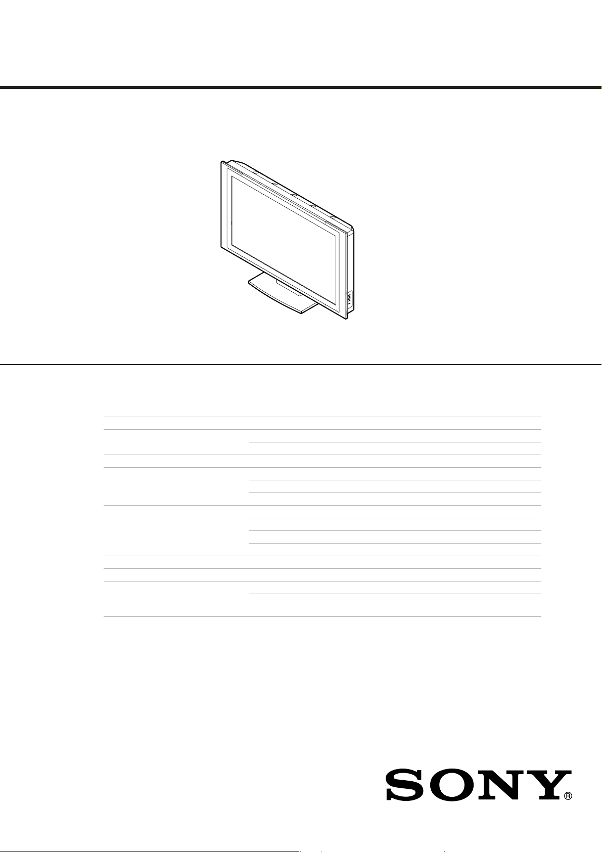
KDE-37/42XS955
SERVICE MANUAL
US Model
Canadian Model
XS2 CHASSIS
SPECIFICATIONS
Panel System Plasma Display panel
Display resolution KDE-37XS955 1024 pixels (horizontal) × 1024 pixels (vertical)
KDE-42XS955
Antenna 75 ohm external terminal for VHF/UHF
Television System NTSC American TV Standard
ATSC (8VSB terrestrial) ATSC compliant 8VSB
QAM on cable ITU-T J.83 Annex B compliant 64/256 QAM
Channel Coverage 2-69
Power Requirements 120V, 60 Hz
Inputs/Outputs
HDMI IN Video 1080i, 720p, 480p, 480i
Terrestrial (analog)
Cable TV (analog)
Terrestrial (digital) 2-69
Cable TV (digital)
Audio Two channel linear PCM 32, 44.1 and 48 kHz,
1024 pixels (horizontal) × 1024 pixels (vertical)
1-125
1-135
16, 20 and 24 bits
FLAT PANEL COLOR TV

Video (IN) 1 Vp-p, 75 ohms unbalanced, sync negative
S Video (IN)
3 total (1 on left side panel)
3 total (1 on left side panel)
Y: 1 Vp-p, 75 ohms unbalanced, sync negative
C: 0.286 Vp-p (Burst signal), 75 ohms
Audio (IN) 500 mVrms (100% modulation)
5 total (1 on left side panel)
Impedance: 47 kilohm
Component Video Input
CONTROL S (IN) Mini jack
2 (Y, P
1
B
, PR)
CONTROL S (OUT)
Digital Audio Optical Output
1Optical rectangular (1)
Y: 1.0 Vp-p, 75 ohms unbalanced, sync negative;
P
B
: 0.7 Vp-p, 75 ohms
R
: 0.7 Vp-p, 75 ohms
P
Mini jack
(PCM/Dolby Digital)
Variable/Fixed Audio (OUT) 1 More than 408 mVrms at the maximum volume
setting (Variable)
More than 408 mVrms (Fixed)
Impedance (output): 2 kilohms
Sub woofer (OUT) Phono jack
™
CableCARD
slot PCMCIA Type I/II
1
Screen Size (measured diagonally) KDE-37XS955 37 inches
KDE-42XS955
42 inches
Speaker Output 25 W × 2 + 50 W woofer
CENTER SPEAKER IN Max. 180 W (6 Ω), 1 kHz, Sensitivity 30 Vp-p
Dimensions (W × H × D) KDE-37XS955 1048 × 679 × 360 mm
3
(41
/8× 26 3/4× 14 1/4 in)
KDE-42XS955
1139 × 752 × 360 mm
7
/8× 29 5/8× 14 1/4 in)
(44
Mass KDE-37XS955 51.0 kg (112 lb 7 oz)
KDE-42XS955
56.5 kg (124 lb 9 oz)
Power Consumption In Use KDE-37XS955: 350 W
KDE-42XS955: 385 W
In Standby 0.5 W
CableCARD Standby KDE-37XS955: 26 W
KDE-42XS955: 26 W
Supplied Accessories Remote Control (1)
RM-Y1004
AA (R6) Batteries (2)
AC power cord (1)
AC plug holder (1)
Cable band (1)
Cable band screw (1)
AC cord clamp (1)
Cleaning Cloth (1)
Operating Instructions (1)
Quick Setup Guide (1)
Warranty Card (1)
Design and specifications are subject to change without notice.
KDE-37XS955/42XS955 (UC) 2

WARNING AND CAUTIONS
A
A
CAUTION
These servicing instructions are for use by qualified service personnel only To reduce the risk of electric shock, do not perform any
servicing other than that contained in the operating instructions unless you are qualified to do so.
WARNING!!
n isolation transformer should be used during any service to avoid possible shock hazard, because of live chassis. The chassis of
this receiver is directly connected to the ac power line.
!
SAFETY-RELATED COMPONENT WARNING!!
Components identified by shading and ! mark on the schematic diagrams, exploded views, and in the parts list are critical for safe
operation. Replace these components with Sony parts whose part numbers appear as shown in this manual or in supplements
published by Sony. Circuit adjustments that are critical for safe operation are identified in this manual. Follow these procedures
whenever critical components are replaced or improper operation is suspected.
ATTENTION!!
Ces instructions de service sont à l’usage du personnel de service qualifié seulement. Pour prévenir le risque de choc électrique, ne
pas faire l’entretien autre que celui contenu dans le Mode d’emploi à moins que vous soyez qualifié faire ainsi.
fin d’eviter tout risque d’electrocution provenant d’un chássis sous tension, un transformateur d’isolement doit etre utilisé lors de tout
dépannage. Le chássis de ce récepteur est directement raccordé à l’alimentation du secteur
!
ATTENTION AUX COMPOSANTS RELATIFS A LA SECURITE!!
Les composants identifies par une trame et par une marque ! sur les schemas de principe, les vues explosees et les listes de pieces
sont d’une importance critique pour la securite du fonctionnement. Ne les remplacer que par des composants Sony dont le numero
de piece est indique dans le present manuel ou dans des supplements publies par Sony. Les reglages de circuit dont l’importance
est critique pour la securite du fonctionnement sont identifies dans le present manuel. Suivre ces procedures lors de chaque
remplacement de composants critiques, ou lorsqu’un mauvais fonctionnement suspecte.
KDE-37XS955/42XS955 (UC) 3
SAFETY CHECK-OUT
After correcting the original service problem, perform the
following safety checks before releasing the set to the customer:
1. Check the area of your repair for unsoldered or poorly-soldered connections. Check the entire board surface for solder
splashes and bridges.
2. Check the interboard wiring to ensure that no wires are
“pinched” or contact high-wattage resistors.
3. Check that all control knobs, shields, covers, ground straps,
and mounting hardware have been replaced. Be absolutely certain that you have replaced all the insulators.
4. Look for unauthorized replacement parts, particularly transistors, that were installed during a previous repair. Point them
out to the customer and recommend their replacement.
5. Look for parts which, though functioning, show obvious signs
of deterioration. Point them out to the customer and recommend their replacement.
6. Check the line cords for cracks and abrasion. Recommend the
replacement of any such line cord to the customer.
7. Check the antenna terminals, metal trim, “metallized” knobs,
screws, and all other exposed metal parts for AC Leakage.
Check leakage as described right.
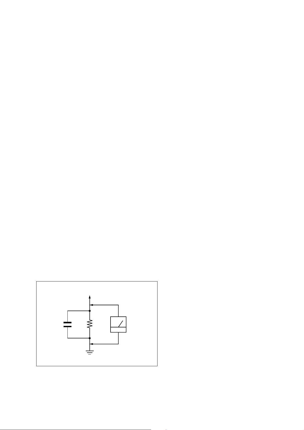
LEAKAGE TEST
The AC leakage from any exposed metal part to earth ground and
from all exposed metal parts to any exposed metal part having a
return to chassis, must not exceed 0.5 mA (500 microamperes).
Leakage current can be measured by any one of three methods.
1. A commercial leakage tester, such as the Simpson 229 or RCA
WT-540A. Follow the manufacturers’ instructions to use these
instruments.
2. A battery-operated AC milliammeter. The Data Precision 245
digital multimeter is suitable for this job.
3. Measuring the voltage drop across a resistor by means of a
VOM or battery-operated AC voltmeter. The “limit” indication is 0.75 V, so analog meters must have an accurate lowvoltage scale. The Simpson 250 and Sanwa SH-63Trd are examples of a passive VOMs that are suitable. Nearly all battery
operated digital multimeters that have a 2 V AC range are suitable. (See Fig. A)
WARNING!!
SAFETY-RELATED COMPONENT WARNING!!
COMPONENTS IDENTIFIED BY SHADING AND MARK !
ON THE SCHEMATIC DIAGRAMS, EXPLODED VIEWS
AND IN THE PARTS LIST ARE CRITICAL FOR SAFE
OPERATION. REPLACE THESE COMPONENTS WITH
SONY PARTS WHOSE PART NUMBERS APPEAR AS
SHOWN IN THIS MANUAL OR IN SUPPLEMENTS PUBLISHED BY SONY. CIRCUIT ADJUSTMENTS THAT ARE
CRITICAL FOR SAFE OPERATION ARE IDENTIFIED IN
THIS MANUAL. FOLLOW THESE PROCEDURES WHENEVER CRITICAL COMPONENTS ARE REPLACED OR
IMPROPER OPERATION IS SUSPECTED.
AVERTISSEMENT!!
ATTENTION AUX COMPOSANTS RELATIFS À LA
SÉCURITÉ!!
LES COMPOSANTS IDENTIFIÉS PAR UNE TRAME ET
UNE MARQUE ! SONT CRITIQUES POUR LA
SÉCURITÉ. NE LES REMPLACER QUE PAR UNE
PIÈCE PORTANT LE NUMÉRO SPECIFIÉ. LES
RÉGLAGES DE CIRCUIT DONT L’IMPORTANCE EST
CRITIQUE POUR LA SÉCURITÉ DU
FONCTIONNEMENT SONT IDENTIFIÉS DANS LE
PRÉSENT MANUEL. SUIVRE CES PROCÉDURES
LORS DE CHAQUE REMPLACEMENT DE
COMPOSANTS CRITIQUES, OU LORSQU’UN MAUVAIS
FONCTIONNEMENT EST SUSPECTÉ.
To Exposed Metal
Parts on Set
0.15 µF
1.5 k
Ω
Earth Ground
AC
Voltmeter
(0.75 V)
Fig. A. Using an AC voltmeter to check AC leakage.
KDE-37XS955/42XS955 (UC) 4

TABLE OF CONTENTS
1. DISASSEMBLY ............................................ 1-1
1-1. SERVICE POSITION ........................................ 1-1
1-1-1. PANELS AND CAP REMOVAL ................. 1-1
1-1-2. WOOFER BLOCK REMOVAL ................... 1-1
1-1-3. REAR COVER ASSY REMOVAL .............. 1-1
1-2. STAND REMOVAL .......................................... 1-2
1-3. REAR COVER ASSY REMOVAL .................. 1-2
1-4. QU BOARD REMOVAL .................................. 1-3
1-5. QM AND QT BOARDS REMOVAL ............... 1-3
1-6. A2FU, DE1, DIC3 AND M1U
BOARDS REMOVAL ....................................... 1-4
1-7. A1U, H2, P AND QH BOARDS REMOVAL
............................................................................ 1-4
1-8. G1, G2F AND K BOARDS REMOVAL .......... 1-5
1-9. F AND H1U BOARDS REMOVAL ................. 1-5
1-10. PLASMA DISPLAY PANEL
ASSY REMOVAL ............................................. 1-6
1-11. H3 AND H4 BOARDS REMOVAL ................. 1-7
1-12. H5 BOARD REMOVAL ................................... 1-7
2. ADJUSTMENTS
and TROUBLESHOOTING .......................... 2-1
2-1. WHITE BALANCE ADJUSTMENT ................ 2-1
2-1-1. Measurement equipment ................................ 2-1
2-1-2. Measuring procedure ..................................... 2-1
2-1-3. Service mode .................................................. 2-1
2-2. TROUBLESHOOTING ..................................... 2-2
3. DIAGRAMS ................................................... 3-1
3-1. BLOCK DIAGRAMS ........................................ 3-1
(1) A1U AND H2 BOARDS .................................. 3-1
(2) A2FU (1/2) BOARD ......................................... 3-2
(3) A2FU (2/2) AND H4 BOARDS ....................... 3-3
(4) DE1 BOARD .................................................... 3-4
(5) DIC3 BOARD ................................................... 3-5
(6) F AND G1 BOARD .......................................... 3-6
(7) G2F BOARD ..................................................... 3-7
(8) K BOARD ......................................................... 3-8
(9) H1U, H3, H5 AND M1U BOARDS ................ 3-9
(10) P BOARD ........................................................ 3-10
(11) QH AND QM BOARDS ................................ 3-11
(12) QT AND QU BOARDS .................................. 3-12
3-2. FRAME DIAGRAMS ........................................ 3-13
3-3. CIRCUIT BOARDS LOCATION ..................... 3-14
3-4. SCHEMATIC DIAGRAMS AND
PRINTED WIRING BOARDS ........................ 3-14
(1) Schematic Diagrams of A1U Board .............. 3-15
(2) Schematic Diagrams of A2FU Board............ 3-19
(3) Schematic Diagrams of DE1 Board .............. 3-22
(4) Schematic Diagrams of DIC3 Board ............. 3-27
(5) Schematic Diagram of F Board ..................... 3-34
(6) Schematic Diagrams of G1 Board ................. 3-35
(7) Schematic Diagrams of G2F Board............... 3-38
(8) Schematic Diagram of H1U and H2 Boards
........................................................................ 3-41
(9) Schematic Diagram of H3 and H4 Boards
........................................................................ 3-42
(10) Schematic Diagram of H5 Board .................. 3-43
(11) Schematic Diagram of K Board .................... 3-44
(12) Schematic Diagrams of M1U Board ............. 3-46
(13) Schematic Diagram of P Board ..................... 3-55
(14) Schematic Diagram of QH Board .................. 3-54
(15) Schematic Diagrams of QM Board ............... 3-55
(16) Schematic Diagrams of QT Board ................ 3-60
(17) Schematic Diagram of QU Board .................. 3-63
3-5. SEMICONDUCTORS ....................................... 3-64
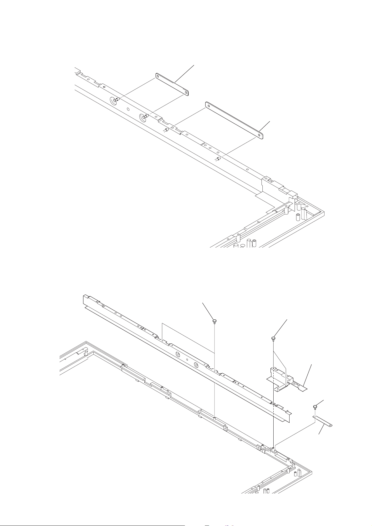
4. EXPLODED VIEWS ...................................... 4-1
4-1. REAR COVER ASSY AND STAND ............... 4-2
4-2. CHASSIS-1 ........................................................ 4-4
4-3. CHASSIS-2 ........................................................ 4-5
4-4. CHASSIS-3 ........................................................ 4-6
4-5. CHASSIS-4 ........................................................ 4-7
4-6. PACKING MATERIALS .................................. 4-8
5. ELECTRICAL PARTS LIST ........................ 5-1
KDE-37XS955/42XS955 (UC) 5
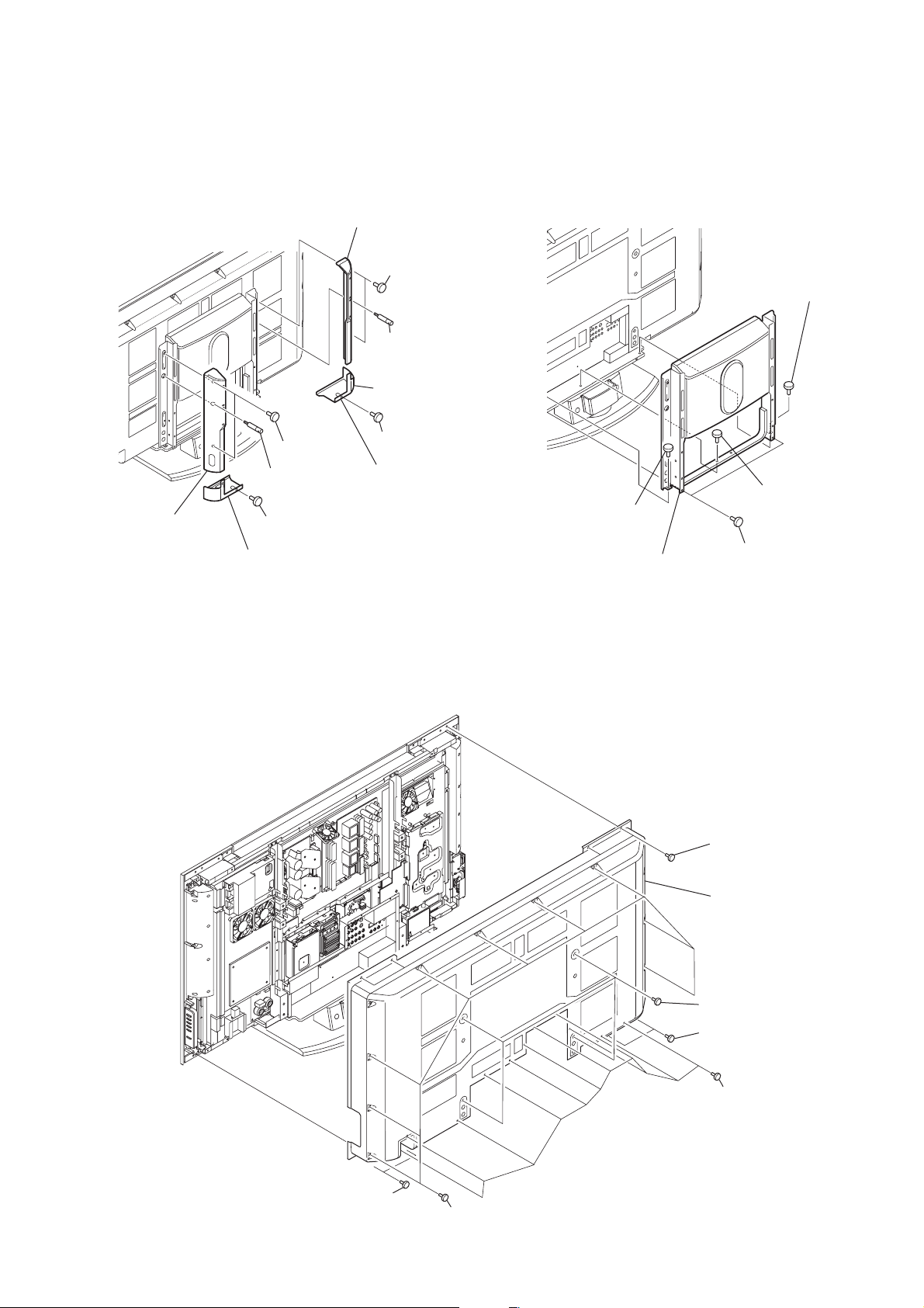
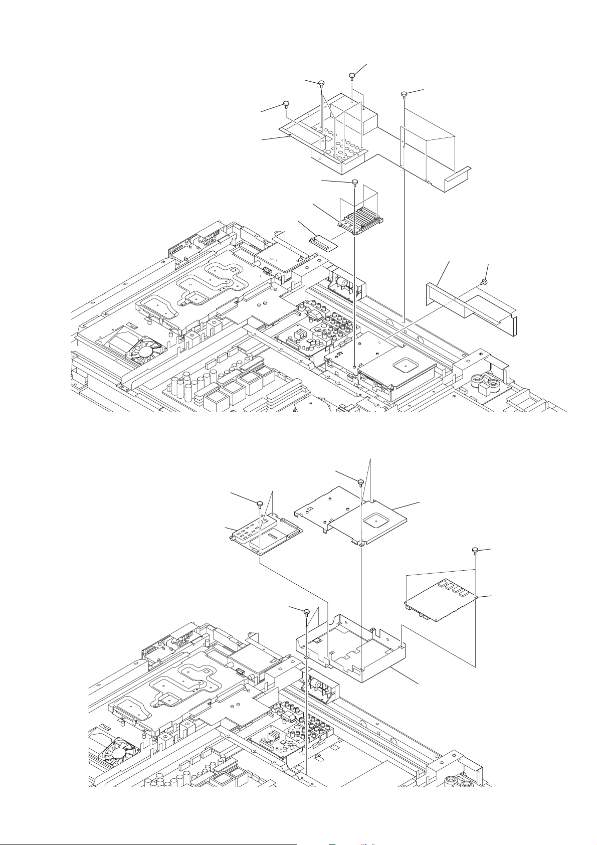
1-1. SERVICE POSITION
1-1-1. PANELS AND CAP REMOVAL
SECTION 1
DISASSEMBLY
1-1-2. WOOFER BLOCK REMOVAL
7 Two screws
(+BVTT 4x6)
1 Screw
(+PSW 4x10)
6 Screw
(HOOK, M5)
5 Cap,bottom(L)
9 Screw
(+BVTP 4x10)
0 Cap,bottom(L)
3 Panel(R),ornament
2 Two screws
(+BVTT 4x6)
1 Screw
(HOOK, M5)
4 Screw
(+BVTP 4x10)
5 Cap,bottom(R)
1-1-3. REAR COVER ASSY REMOVAL
1 Screw
(+PSW 4x10)
4 Woofer block
3 Two screws
(BUTTON HEAD 6x40)
2 Two screws
(+BVTP 4x10)
4 Four screws
(+PSW 4x6)
3 Two screws
(+PSW 4x6)
6 Rear cover assy
1 Six screws
(+PSW 5x10)
3 Two screws
(+PSW 4x6)
2 Eleven screws
(+PSW 3x6)
5 Nine screws
(+BVTP 4x16)
KDE-37XS955/42XS955 (UC) 1-1
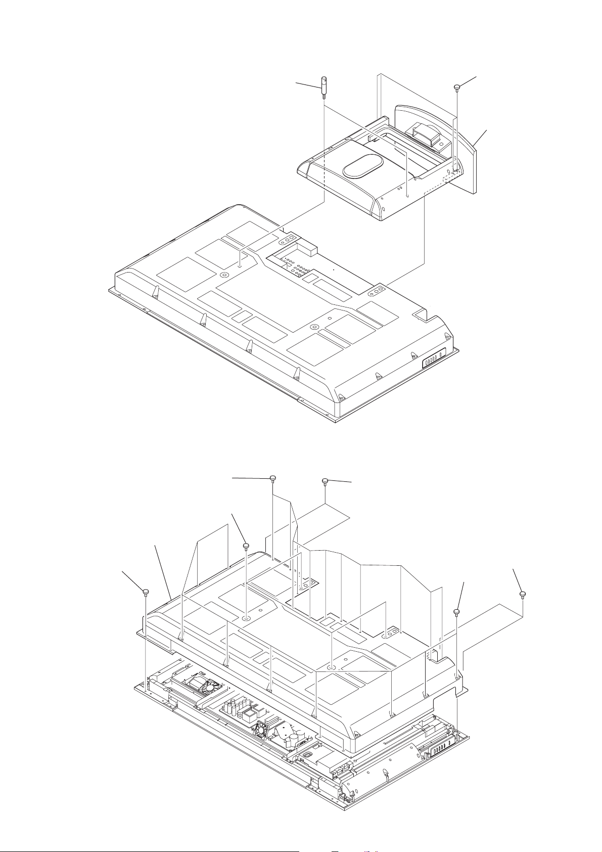
1-2. STAND REMOVAL
1 Two screws
3 Stand
2 Four screws
(+PSW (M5))
1-3. REAR COVER ASSY REMOVAL
2 Eleven screws
(+PSW 3x6)
1 Six screws
6 Rear cover assy
4 Four screws
(+PSW 4x6)
(+PSW 5x10)
3 Four screws
(+PSW 4x6)
5 Nine screws
(+BVTP 4x16)
3 Four screws
(+PSW 4x6)
KDE-37XS955/42XS955 (UC) 1-2
1-4. QU BOARD REMOVAL
6 Screw
(+PSW 3x8)
7 Twrminal board
4 Five screws
(+BVTP 3x12)
8 Four screws
(+PSW 3x8)
9 Pod assy
0 QU board
5 Two screws
(+BVTP 4x16)
3 Four screws
(+PSW 3x6)
1-5. QM AND QT BOARDS REMOVAL
5 Two screws
(+PSW 3x6)
6 QT board
1 Two screws
(+PSW 3x6)
2 ATSC bracket
2 Shield ATSC top
1 Two screws
(+PSW 3x6)
7 Two screws
(+PSW 3x6)
3 Two screws
(+PSW 3x6)
4 QM board
8 Shield ATSC bottom
KDE-37XS955/42XS955 (UC) 1-3
1-6. A2FU, DE1, DIC3 AND M1U BOARDS REMOVAL
8 Four screws
(WASHER HEAD (+P 3X5))
2 Two screws
(+PSW 3x6)
3 Shield DM top
6 Four screws
(WASHER HEAD (+P 3X5))
4 Four screws
(WASHER HEAD (+P 3X5))
5 DE1 board
qa Shield DM bottom
9 M1U board
7 DIC3 board
1 A2FU board
0 Four screws
(+PSW 3x6)
1-7. A1U, H2, P AND QH BOARDS REMOVAL
7 Screw
(+PSW 3x10)
8 Four screws
(+BVTP 3x12)
9 QH board
0 Screw
(+BVTP 3x12)
qa Two screws
(+PSW 3x10)
5 Two screws
(+BVTP 3x12)
6 H2 board
0 Screw
(+BVTP 3x12)
qs Connector panel assy
1 Three screws
(+PSW 3x6)
4 A1U board
2 P board
3 Four screws
(+PSW 3x6)
KDE-37XS955/42XS955 (UC) 1-4
1-8. G1, G2F AND K BOARDS REMOVAL
d
6 Two screws
(+BVTP 3x12)
2 Two screws
(+BVTP 4x16)
8 Two screws
(+BVTP 3x12)
7 Control panel assy
9 H1U board
1 Two screws
(+PSW 3x6)
4 Two screws
(+PSW 3x6)
5 F board
3 Bottom plate
1 Two screws
(+PSW 3x6)
2 Shield K upper
4 K board
0 G2F board
3 Two screws
(+PSW 3x6)
5 Four screws
(+PSW 3x10)
9 Four screws
(+PSW 3x6)
7 Three screws
(+PSW 3x6)
8 G1 boar
6 Shield K bottom
1-9. F AND H1U BOARDS REMOVAL
KDE-37XS955/42XS955 (UC) 1-5
1-10. PLASMA DISPLAY PANEL ASSY REMOVAL
KDE-42XS955
qa Screw
(+PS 4x8)
8 Three screws
(+BVTP 4x16)
9 Five screws
(+PSW 4x8)
0 Shield SUS(L)
8 Three screws
(+BVTP 4x16)
0 Shield SUS(L)
3 Four screws
(+P 4x16)
qd Four screws
(+PSW 4x8)
KDE-37XS955
9 Six screws
(+PSW 4x8)
6 Six screws
(+PSW 4x8)
qs Shield A bottom
qf Four screws
(+PSW 4x8)
5 Four screws
(+BVTP 4x16)
7 Shield SUS(R)
qg Plasma disply panel ASSY
4 Spaker(L)
1 Four screws
(+P 4x16)
2 Speaker(R)
KDE-37XS955/42XS955 (UC) 1-6
1-11. H3 AND H4 BOARDS REMOVAL
1 H4 board
2 H3 board
1-12. H5 BOARD REMOVAL
3 Two screws
(+BVTP 4x16)
1 Two screws
(+BVTP 4x16)
2 Corner bracket
5 Screw
(+BVTP 3x12)
6 H5 board
KDE-37XS955/42XS955 (UC) 1-7E
SECTION 2
ADJUSTMENTS and TROUBLESHOOTING
2-1. WHITE BALANCE ADJUSTMENT
When the Panel or DE1 Board is replaced or is repaired, W/B
should be adjusted.
2-1-1. Measurement equipment
1. Color analyzer (CA-100 manufactured by MINOLTA)
2. Signal generator (ASTRO DESIGN VG-828D)
2-1-2. Measuring procedure
1. Dab the W/B adjustment jig (CA-100) at the glass face of the
panel.
2. Connect the Signal generator (VG-828D) to the component
terminal.
3. Input All-white signal (70%).
4. Make the settings as follows.
• Set the quality mode to PRO.
• Set the PICTURE to MAX.
5. Set the color temp, be adjusted cool.
6. Adjust the color temperature of the “highlight” side with the
following items of service mode menu, fixed a avlue of one of
RGBs 255.
*Operation Register
Service mode “53 FHP_I_1”
36 : RGAIN
37 : GGAIN ×××
38 : BGAIN ×××
Note: Refer to section 2-1-3 for adjustment in service mode.
×××
4. After the adjustment is completed, save the data using the
MUTE and ENTER keys.
7. Adjust Cool, Neutral, Warm of each color temperature.
Adjustment target values:
MODE x y
COOL
NEUTRAL
WARM
0.2684 ± 0.003 0.2700 ± 0.003 13550K + 0MPCD
0.2849 ± 0.003 0.2931 ± 0.003 9300K + 0MPCD
0.2951 ± 0.003 0.3044 ± 0.003 8000K + 0MPCD
2-1-3. Service mode
1. How to Enter Service Mode
1) Turn on the main power switch to place this set in standby
mode. (The LED will light red.)
2) Press the buttons on the commander as follows to enter
service mode.
5
(VOLUME +)(DIGIT 5)(DISPLAY) (POWER)
2. Press the JUMP key on the commander three times.
3. How to Adjust
“53 FHP_I_1”
Category name.
(Can be changed with the 2 and 5 keys on the commander.)
36 RGAIN
×××
Data Can be changed with the 3 and
6 keys on the commander.
Item Name
Item No.
Can be changed with the 1 and
4 keys on the commander.
Enter the
“Service mode”
KDE-37XS955/42XS955 (UC) 2-1

2-2. TROUBLESHOOTING
Twin View
Problem Possible Remedies
I cannot get Twin View to work s If you are using a cable box to unscramble all channels (as shown on page 26), you
There is no Twin View window,
or it is just static
Tw in View cannot display
anything but TV channels
Tw in View displays the sa m e
program in both windows
cannot use the Twin View feature. This is because the cable box can unscramble
only one channel at a time. But if you need the cable box to unscra mble only some
(usually premium) channels, you can use Twin View for unscrambled channels if
you connect both a cable and cable box, as shown on page 25.
s You can use T win V iew to vie w a signal from a different source that is connected to
the TV's A/V jacks (such as a VCR or DVD player) in the second window by
pressing the TV/VIDEO button while in Twin View.
s Digital sources, as well as any sources connected to the VIDEO 4, VIDEO 5,
VIDEO 6 inputs, d isplay in the left window, but not in the right wi ndows.
s Be sure the Twin View window is set to a video input or channel that has a signal
airing.
s You might be tuned to a video input with nothing connected to it. Try cycling
through the video inputs by pressing the TV/VIDEO button.
s Try cycling thr ough the video inputs by pressing the TV/VIDEO button. Check
that the Label Video Inputs option is not set to Skip. (See the Setup Menu on
page 105.)
s Both Twi n V ie w windo ws mig ht be set to the same cha nnel. T ry chan ging channels
in either window.
Remote Control
Problem Possible Remedies
Remote control does not oper a tes The batteries could be weak. Replace the batteries.
s Check the orientation of the batteries.
s Press the TV (FUNCTION) button. You may have inadvertently pressed the
SAT/CABLE (FUNCTION) button, which changes the remote control to SAT or
CABLE mode.
s Make sure the TVís power cord is connected securely to the wall outlet.
s Locate the TV at least 3-4 feet away from fluorescent lights.
Cannot change channels with
the remote control
Remote control does not operate
non-Sony video equipment
CableCARD
™
s If you are using the TV to chan ge channels, first press the TV (FUNCTION)
button.
s If you are using another device to change channels, be sure you have not
inadvertently switched your TV from the channel 3 or 4 setting. Use the Channel
Fix option to ìfixî the channel based on the hookup you used (see page 99) .
s If you are using another device to change channels, be sure to press the
FUNCTION button for that device. For example, i f you are using your cable box
to change channels, be sure to press the SAT/CABLE (FUNCTION) button.
s If you replaced the batteries to the remote recently, the code numbers for the video
equipment may need to be reset.
s There may be more than one code for the equipment that you are attempting to
operate.
s There is a possibility that some non-Sony equipment cannot be operated by your
Sony TV remote.You may need to use the equipmentís origi nal remote control.
Problem Possible Remedies
Problems using CableCARD™
or CableCARD
™
services
s Check that the CableCARD
s The CableCARD
can receive digital cable TV services. See the activation instructions on page 51.
s Check the Diagnostics and CableCARD
can be useful in providing information to an authorized technician or repair
person.)
s Contact your cable TV provider.
™
™
must be activated by your local cable TV provider before you
is inserted properly (see page 51).
™
menu options (see page 108). (This
KDE-37XS955/42XS955 (UC) 2-2

Channels
Problem Possible Remedies
Cannot receive upper channels
(UHF) when using an antenna
TV is fixed to one channel s Use Auto Program in the Channel Menu to add receivable channels that are not
Cannot receive any channels
when using cable TV
Cannot receive or select
channels
Some digital cable channel s are
not being displayed
s Press ANT to select the VHF/UHF input (see page 57).
s Use Auto Program in the Channel Menu to add receivable channels that are not
presently in the TVís memory (see page 99).
presently in the TVís memory (see page 99).
s Check your Channel Fix settings (see page 99).
s Use Auto Program in the Channel Menu to add receivable channels that are not
presently in the TVís memory (see page 99).
s Press ANT to select the CABLE input (see page 57).
s Use Auto Program in the Channel Menu to add receivable TV channels that are
not presently in TV memory (see pag e 99).
s Certain cable TV compani es have limitations on the broadcast of digital cable
channels. Check with your cable TV company for more information.
s Check with your cable TV company if the channels are scrambled or encrypted.
You will need a CableCARD or a separate set-top box to view those channels.
s Some optional digital cable broadcast formats may no t be supported. If your cable
TV company is br oadc astin g digita l sign al s in unsup p orted broadc as t format s, you
will need a separa te s et-top box pro vi ded b y your c abl e TV com pan y to vie w thos e
channels.
s The digital cable channel may be set to Hide in the Channel Menu (see page 99).
s Use the Digital Channels feature to search for new digital channels (see page 99).
Memory Stick
Problem Possible Remedies
Image does not display/C annot
see all files
JPEG image displays
undesirable motio n or flicker in
full screen
Rotation not saved after
Memory Stick is ejected or
Memory Stick Viewer is closed
Cannot show (or hide) file
information in full screen or
Slide Show
Cannot set print quantity s The Memory Stick might be lo c k e d. Unloc k the Me mo ry Stick and try rotating the
Cannot see Menu s Press V to display the Menu again.
Cannot hear audio whil e using
Memory Stick
Not all MP3 files on Memory
Stick are included when the
Music /Complete List option is
selected (page 88)
Cannot see MP3 list to play
music
MP3 file does not play back
correctly
s Make sure the image file is a JPEG (.jpg, .jpeg) file or an MPEG1 (.mpg, .mpeg)
file.
s Make sure the Memory Stick is inserted properly (see page 78).
s Check the Filter option setting (see page 89).
s Check the Select Folder setting (see page 89) and ensure that files are either in
DCF directories if Digital Camer a Folders is selected (see page 89), or in the
currently selected folder if Select a Folder is selected (see page 89).
s The maximum number of files the Memory Stick Viewer can display is 2,000 files
total, including all JPEG, MPEG1, and MP3 files.
s If you are using a Memory Stick with the Memory Select function, try changing
the position of the A/B select switch.
s JPEGs captu red using a digital video camera may appear to display motion in fu ll
screen. This is a result of the way digital video cameras record still images, and is
not a result of a malfunction with the TV.
s The Memory Stick might be lo c k e d. Unlo ck the Me mo ry Sti ck a n d try rotating the
image again.
s The file might not have information (EXIF data) that is usually generated when a
digital camera records a photo. In this case, it is not possible to save the rotation.
s There might be insuf ficient space on the Memory Stick to save the rotated file. Try
deleting one or more files and rotating the image again.
s Set the File Information option to On or Off (see page 88).
image again.
s Check the TVís volume or Speaker (page 96) settings.
s To hear JPEG voice memo in full screen view, select the Digital Camera Folders
option and set the Filter option to Show All Print Marks.
s Check that the Music option is not to set to Off (see page 88).
s The Memory Stick Viewer can display a maximum of 2,000 files total, including
all JPEG, MPEG1, and MP3 files.
s Make sure that the file is named with the file extension (.mp3).
s MP3 files on your Memory Stick only can be played as background music during a
Slide Show (see page 88).
s The Memory Stick Viewer supports only MP3 files with a fixed data rate of
128 kbps (kilobit s per second).
KDE-37XS955/42XS955 (UC) 2-3
MP3 files on the Memory Stick
are not listed
Music files are playing in wrong
order
MPEG1 movie does not play
back correctly
Problem Possible Remedies
MPEG1 quality is poor when
enlarged (page 86)
Error message is displayed s No Memory Stick There is no Memory Stick in the slot.
Error icon is displayed The file is not a vali d MPEG1 or JPEG format, or it is a
s Only MP3 files that are named with the file extension (.mp3) are displayed in the
list.
s MP3 files are played in alphabetical order, according to the folder in which they
are stored. If you want t o change the playlist order, rename your files
alphabetically in the order in which you want them to play.
s Some variations o f M PEG1 movies may not be compatible with the Memory Stick
Viewer.
s The quality of the movie when enlarged depends on the resolution of the MPEG1
file. See your cameraís instruction manual for details.
s Memory Stick
Locked
s Memory Stick Error The Memory Stick in the slot might be damaged; try a
s Format Error The Memory Stick m ay h a v e be en formatte d us ing a PC
The lock mechanism on the Memory Stick is engaged.
different Memory Stick.
or other device that is not compatible with cameras.
progressive JPEG (whi ch is not supported).
The thumbnail is not DCF-compatible.
The file is a JPEG or an MPEG1, but the thumbnail is
unreadable.
The file is unreadable.
Audio
Problem Possible Remedies
Good picture, no sound s Press MUTING so that the word Muting disappears from the screen (see page 56).
s Make sure the Speaker optio n is set to On in the Audio Menu (see page 96 ).
s Make sure the MTS option is set to Stereo or Mono (see page 95).
Cannot gain enough volume
when using a cable box
Sound seems weak or
insufficient
Cannot raise the volume on
external audio speakers
There is no sound from
WOOFER
s Increase the volume of the cable box using the cable box’s remote control. Then
press TV (FUNCTION) and adjust the TVís volume.
s The TV’s audio might be set to Auto SAP or Mono, when it might be better set to
Stereo. In the Audio Menu (see page 95), set the MTS setting to Stereo. If
already set to Stereo, switch to Mono (which may reduce backgr ound noise
during weak stereo broadcasts).
s If the Speaker option is set to Off and the Audio Out option is set to Fixed (in
order to output the sound to your audio system) use your audio receiver to adjust
the sound (see page 96). Or, to use the TV remote control, set the Audio Out
option to Variable.
s To turn on the TV speakers, set the Speaker option to On (see page 96).
s Check the screen if there i s a di splay message stating the WOOFER is
disconnected. If the message i s shown, you may need to contact yo ur dealer or
Sony Customer Information Service Center to check the connection.
KDE-37XS955/42XS955 (UC) 2-4

Video
Problem Possible Remedies
No picture (screen not lit), no
sound
Dark, poor or no picture (screen
lit), good sound
No color./Dark picture./
Color is not correct.
Only snow and noise appear on
the screen
Dotted lines or stripes s Adjust the antenna.
Double images or ghosts s Using a highly directional outdoor antenna or a cable may solve the problem.
Striped noise during
playback/recording of a VCR
Image left on screen s Perform image retention recovery. (see page 98)
The screen flickers when
turning on the TV.
ìBlack boxî on screen s You have selected a text option in the Setup Menu and no text is available. (See
Bars appear at the top and
bottom of the screen
Certain programs on DVD or
other digital sources display a
loss of detail, especially during
fast-motion or dark scenes
s If your TV does not turn on, and a red light keeps flashing, your TV may need
service. Call your local Sony Service Center.
s Make sure the power cord is plugged in.
s Press the POWER button on the right side of the TV.
s Press the TV/VIDEO button to cycle through the connected video sources.
s Try another channel; it could be station trouble.
s Adjust the Picture option in the Video Menu (see page 92).
s Adjust the Brightness option in the Video Menu (see page 92).
s Check the antenna/ cable connections.
s Press the PICTURE (MODE) button to select the desired Picture mode
(see page 56).
s Adjust the Color option in the Video Menu (see page 92) .
s Check the antenna/ cable connections.
s Try another channel; it could be station trouble.
s Press ANT to change the input mode (see page 57).
s Move the TV away from noise sources such as cars, neon signs, or hair-dryers.
s Video head interference. Keep your VCR away from the TV.
s Leave a space of 30 cm (11 7/8 inches) between your VCR and the TV to avoid
noise.
s Avoid installing your VCR in front of the TV or at the side of the TV.
s Use the Screen Saver function (see page 98).
s This is caused by feature of the Plasma Display Panel, and does not indicate a
malfunction of the TV.
page 104 to reset Setup selections.) To turn off this featu re, set the Caption Vision
option to Off. If you were trying to select closed captioning, select CC1 instead of
TEXT 1-4.
s Some wide-screen programs are filmed in aspect ratios that are greater than 16:9,
such as 2.35:1. (This is especially common with theatrical releases). Your TV will
show these programs with bars at the top and bottom of the screen. For more
details, check the documentation that came with your DVD (or contact your
program provider).
s The compression used by certain digital broadcasts and DVDs may cause your
TVís screen to display less detail than usual, or cause artifacts (small blocks or
dots, pixelations) to appear on your screen. This is due to your TVís large screen
and ability to show very fine detail, and is normal for certain digitally recorded
programs. Adjust the reality/clarity in the DRC Palette option (see page 93) to
optimize the picture while viewing these sources.
KDE-37XS955/42XS955 (UC) 2-5

General
Problem Possible Remedies
How to reset TV to factory
settings
How to restore V ideo settin gs to
factory settings
How to restore Audio settin gs to
factory settings
Cannot cycle through the other
video equipment co nnected to
the TV
Cannot operate Menu s If a Menu option appears in gray, this indicates that the TV is in a state in which
Lost password s In the password screen (see page 101), enter the following master password: 4357.
TIMER LED on front panel is lit s The LED (see page 16) blinks when the TV is turned on, then shuts off when the
Digital cable box does not work s If you are connecting a VCR and digital cable box u sing a sp litte r, as described on
Cannot record digital channels
to VCR
s Turn on the TV. While holding down the RESET button on the remote control,
press the POWER button on the right side of the TV. (The TV will turn itself off,
then back on again.) Release the RESET button.
s Press the RESET button on the remote control while in the Video Menu (see p a ge
92).
s Press the RESET button on the remote control while in the Audio Menu (see page
95).
s Be sure the Label Video Inputs option is not set to Skip (see page 105).
the Menu option is not available.
The master password clears your previous password; it cannot be used to
temporarily unblock chann el s.
picture is displayed. If the LED blinks continuously, this may indicate the TV
needs service. When lit, indicates that the timer is set (page 107). When the timer
is set, this LED will remain lit even when the TV is turned off.
page 32, you must use a special bi-direc tional spli tter that is d esign ed to wo rk with
your digital cable box. Contact your cable TV company for details.
s Only analog channels can be recorded to your VCR.
KDE-37XS955/42XS955 (UC) 2-6E
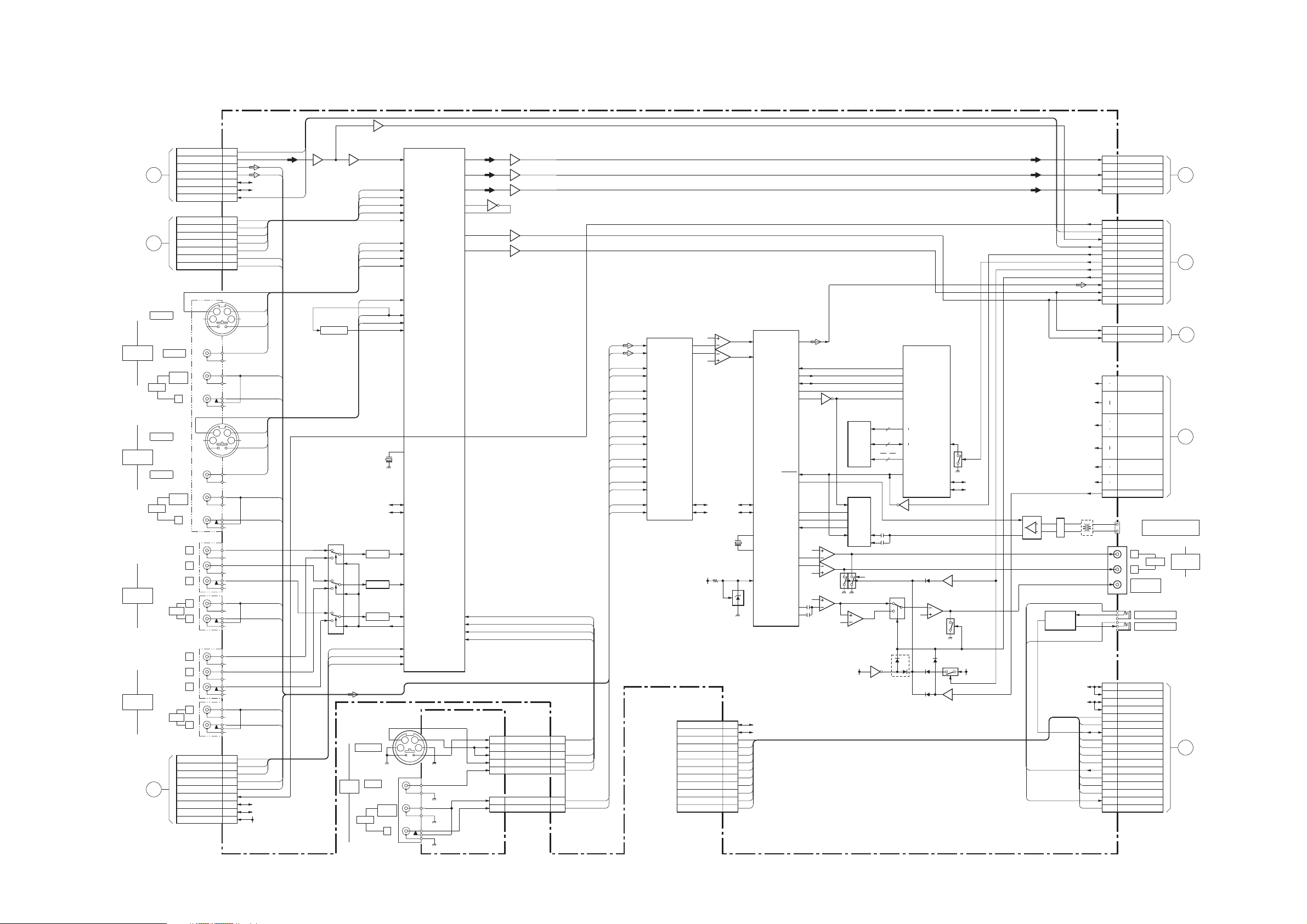
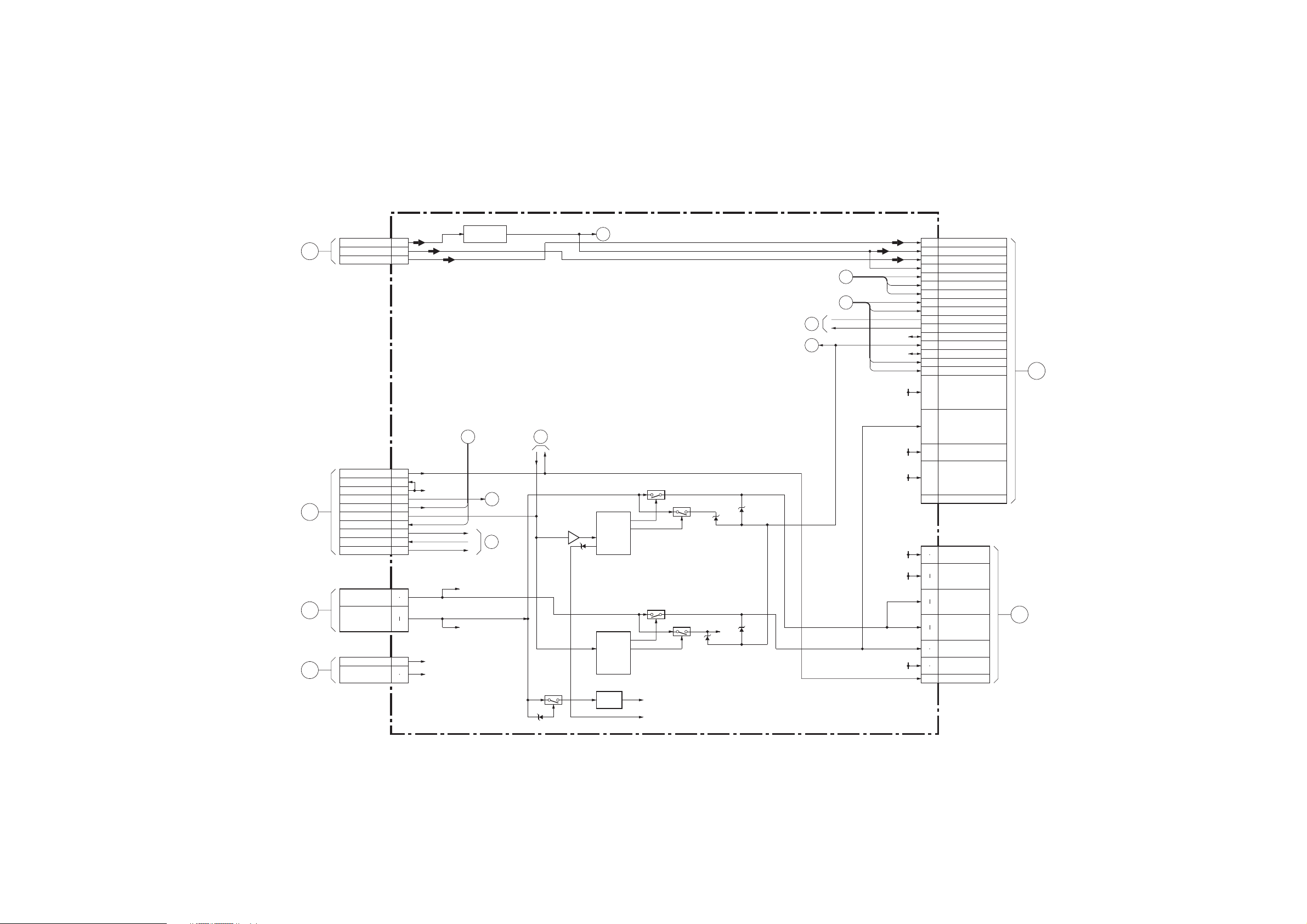
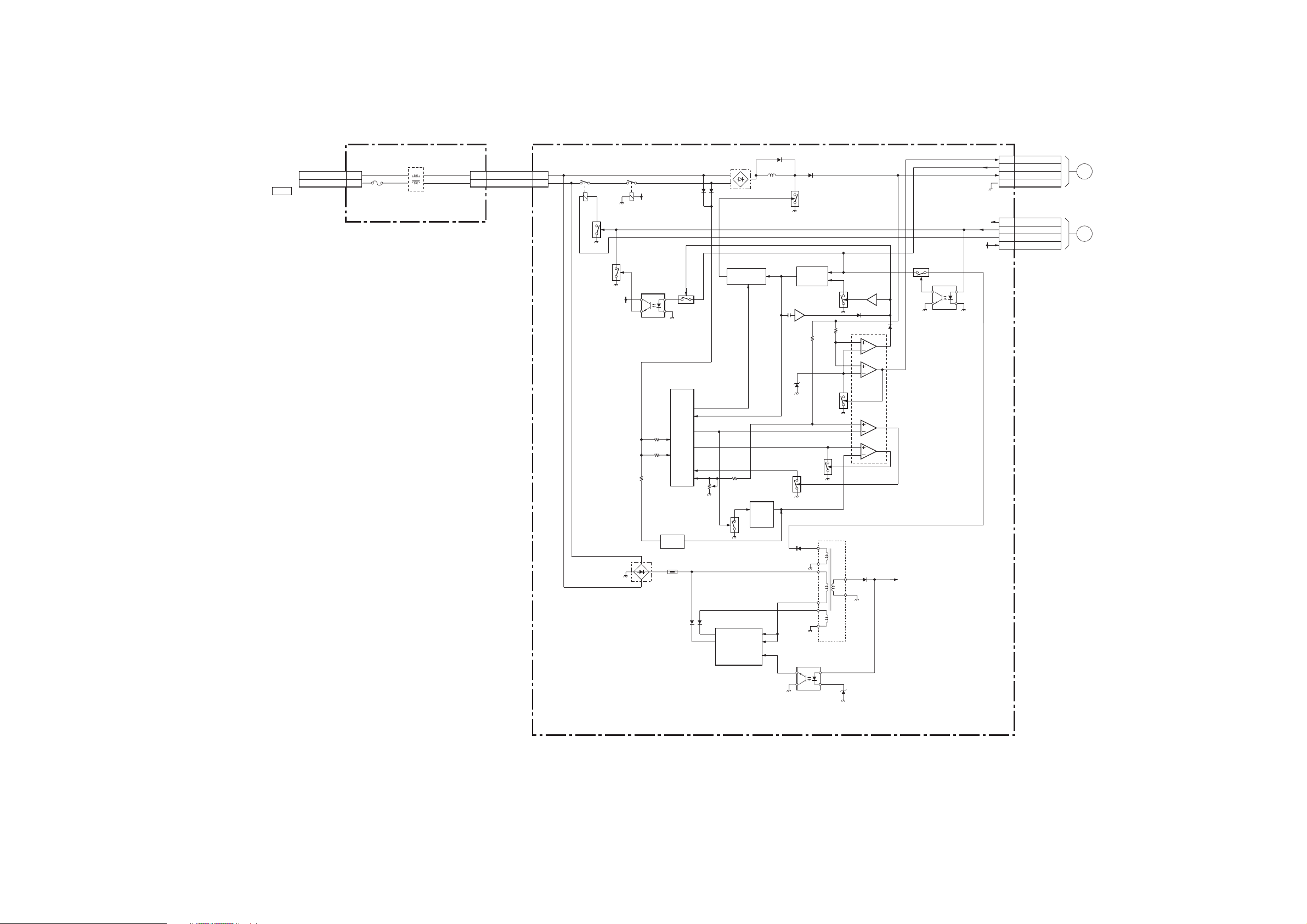
3-1. BLOCK DIAGRAMS
(1) A1U AND H2 BOARDS
SECTION 3
DIAGRAMS
TO
QT BOARD
CN7901
TO
QM BOARD
CN7309
VIDEO IN
3
VIDEO IN
1
HD/DVD IN
4
HD/DVD IN
5
TO
P BOARD
CN9504
N
O
S VIDEO
AUDIO
S VIDEO
VIDEO
AUDIO
A
VIDEO
L
(MONO)
R
L
(MONO)
R
AUDIO
AUDIO
CN005
AFTM
TU1V
TU1R
TU1L
SCLK
SDAT
AGC MUTE
CN006
Pr
Pb
Y
H
V
R
L
J309
SW1
SW2
J304
3P
R
P
P
B
Y
L
R
J302
J310
3P
R
P
B
P
Y
L
R
J300
2P
CN002
Y
PB
PR
L
R
RESET
SDA
SCL
9V
Q305
AFT1
1
2
AUDIO R
AUDIO L
SCL
SDA
CR
CB
HS
VS
V3_Y
V3_C
V3_SSW
V3_V
V1_Y
V1_C
V1_SSW
V1_V
COMP1_L
COMP1_R
COMP2_L
COMP2_R
SDA
SCL
SW9V
Y
ATSC R
ATSC L
V3_L
V3_R
V1_L
V1_R
Y
PB
PR
HDMI_L
HDMI_R
R
L
4
6
8
9
10
A2
A4
A6
B1
B2
B4
B6
43
1
2
V1
L1
R1
43
1
2
V2
L2
R2
R
R
13
11
9
7
6
4
3
2
1
Q317
VIDEO
AGC1
Q302-304
SYNC SEP
IC404
8
9
11
14
16
1
Y
PB
PR
AUDIO L/R
Q315
6
7
5
12
3
2
VIDEO2
INPUT
Y
CB
CR
HS
VS
V3_V
V3_Y
V3_C
V3_SSW
V1_V
V1 V
V1_C
V1_SSW
X302
4MHz
Q410
BUFFER
Q411
BUFFER
Q412
BUFFER
S VIDEO
VIDEO
AUDIO
SCL
SDA
L
(MONO)
R
VIDEO SW
79
IN1_CV
40
IN1O_Y
41
IN10_CB
42
IN10_CR
43
IN10_L1/H
44
IN10_L2/V
17
IN6_CV
18
IN6_Y
19
IN6_C
16
IN6_S
12
IN5_CV
13
IN5_Y
14
IN5_C
11
IN5_S
51
EXT_CLK/XTAL
76
SCL
77
SDA
35
IN9_CR
34
IN9_CB
33
IN9_Y
74
DC_OUT
26
IN8_Y
27
IN8_CB
28
IN8_CR
J1101
6P
34
1
2
J1102
V
L
R
IC303
CV/YOUT1
C/CBOUT1
CROUT1
SEL_OUT1
SYNC_IN1
CV/YOUT2
C/CBOUT2
IN4_CV
IN4_Y
IN4_C
IN4_S
Q316
Y
58
B-Y
59
R-Y
60
56
55
67
68
7
8
9
6
Q314
Q313
Q318
Q320
Q321
CN1102 CN004
CN1104
V2_SW
2
V2 S2
4
V2 C
6
V2 Y
8
10
V2 V
2
V2 L
4
V2 R
H2
SUB_Y/CB/Y
SUB_C/CB
V2_SSW
V2_SSW
1
2
V2_C
4
V2_Y
6
V2_V
8
10
12
V2_V
V2_Y
V2_C
V2 L
V2 R
AUDIO L
L
R
AUDIO R
ATSC_L
ATSC_R
V3_L
V3_R
V1_L
V1_R
COMP1_L
COMP1_R
COMP2_L
COMP2_R
HDMI_L
HDMI_R
V2_L
V2_R
22
23
28
29
4
5
1
2
10
11
13
14
16
17
19
20
IC507
AUDIO SW
IN8_L
IN8_R
IN10_L
IN10_R
IN2_L
IN2_R
IN1_L
IN1_R
IN4_L
IN4_R
IN5_L
IN5_R
IN6_L
IN6_R
IN7_L
IN7_R
LOUT1
ROUT1
SCL
SDA
39
37
31
32
SW9V
CN304
CLK_S
DAT_S
B_INT
TVM_UDP
TVM_UDM
TVM_VBUS
IFP_UDP
IFP_UDM
IFP_VBUS
PAN_UDP
PAN_UDM
PAN_VBUS
IC526
3
2
6
5
SCL
SDA
X501
1
7
SCL
SDA
1
IC514
1
2
3
5
6
7
8
9
10
11
12
13
56
57
2
3
71
7218.432MHz
39
3
2
IC522
AUDIO PROCESSOR
SC1_IN_L
SC1_IN_R
I2S_DEL_IN
I2S_DEL_OUT
I2S_DEL_CS
AUDIO_CLOCK
_CONTROL_OUT_0
SCL
SDA
XTAL_IN
XTAL_OUT
AHVSUP
SCL
SDA
SPDIF
_OUT
DVSUP
_OUT
RESET
DIGITAL
I2C_CL
I2C_WS
I2C DAIN1
SC1_OUT_L
SC1_OUT_R
SC2_OUT_L
SC2_OUT_R
AUDIO L/R
76
8
9
10
11
74 2 4
78
4
5
7
37
36
34 2
33
A1U
CN306
5
MAIN_Y/CV
1
MAIN_C/CB
MAIN_CR
3
CN001
HDMI RST
1
AFT MAIN
2
TU_H_MAIN
4
AGC_ATT
6
AD_RST
7
AD_MUTE
8
LINE MUTE
9
SP MUTE
11
SPDIF
15
SUB_C
18
20
SUB_Y
CN301
SUB_C
12SUB_Y
CN010
1
STBY5V
2
5
SW9V
7
9
11
D5V
12
15
A5V
18
24
3.3V
25
27
11V
28
30
AC_RLY
J305
J307
L
R
SUBWOOFER
OUT(VAR)
CONTROL S IN
CONTROL S OUT
CN011
I2C_SCL
3
I2C_SCL
4
I2C_SDA
7
I2C_SDA
8
B_INT
9
USBDPLS
13
SIRCS
14
USBDMNS
15
USBCONNECT
17
JIG_VBUS
19
JIG_UDP
21
UARTRXDP
22
JIG_UDM
23
PAN_UDM
25
PAN_UDP
27
USER_TXD
28
29
PAN_VBUS
A2FU(1/2)BOARD
A2FU(2/2) BOARD
AA
A2FU(1/2)BOARD
CENTER SPEAKER IN
180W(6 )MAX
AUDI0 IN
AUDIO
(VAR/FIX)
J303
J301
A2FU(2/2)BOARD
59
IISM_OUT
13
IISM_IN
8
BIT_CLK
7
LR_CLK
11
A0-A16
17
IO0-I07
WE/OE
1
2
7
8
2
1821
IC502
D505
FCLK
A0
A16
IO0
IO7
RST
Q509
5
1
IC512
IC524
SRAM
IC521
ADC
11
12
10
9
13
IC504
5
7
6
2
1
3
IC501
3
Q504
Q503
16
IC501
5
7
6
D5V
Q505
IC523
DELAY IC
MUTE
IC510
2
3
D509
D510
D609
SCL
SDA
Q508
1
Q502
Q514
Q515
Q512
Y
B-Y
R-Y
AFT1
AGC1
AUDIO L/R
STBY5V
SW9V
D5V
6
Q510
SCL
SDA
POL
CENT
STBY5V
2
5
IC500
MAIN_LOG
Q306-Q312
U2_TX
MAIN_LOG
U2_TX
MATREX
IN-OUT
CTRL
A5V
3.3V
SUB11V
T501
SCL
SDA
(VIDEO SW,AUDIO SW,
AUDIO PROCESSOR,INPUT TERMINAL)
B
TO
CN8209
G
TO
CN8205
TO
M1U BOARD
CN7005
D
TO
CN8206
E
TO
CN8207
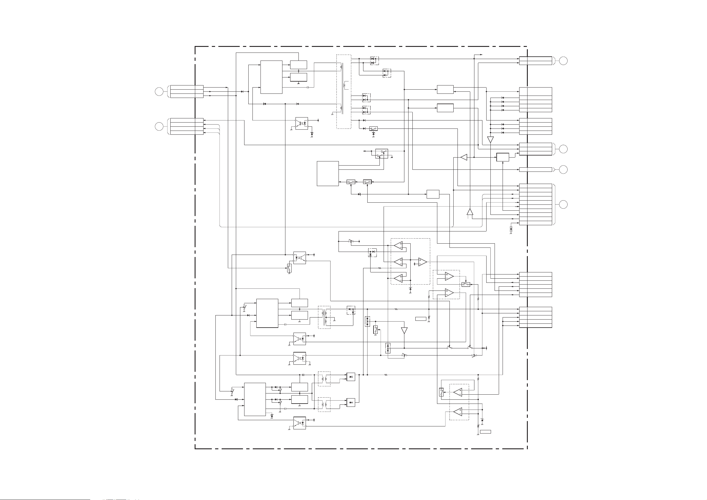
KDE-37XS955/42XS955 (UC) 3-1
(2) A2FU (1/2) BOARD
B
TO
A1U BOARD
CN306
C
TO
G2F BOARD
CN6004
J
TO
G2F BOARD
CN6008
F
TO
G2F BOARD
CN6009
CN8209
MAIN-Y/CV
MAIN-CR
MAIN-C/CB
CN2005
AC_RLY
P_SW
STBY5V
+B_OVP
PS_PROT
POW_CTL
PANEL_ON
FAN_ERR
FAN_DRV
THRMO_G
CN2001
SUB6.5V
SUB11V
CN2004
ATSC5V
SW9V
Q2015-2018
Y
1
R-Y
3
5
3
4
6
7
8
9
10
11
12
13
3
4
8
10
3
5
6
B-Y
STBY5V
ATSC5V
SW9V
BUFFER
TO 2/2
5
SUB6.5V
SUB11V
7
6
TO 2/2
TO 2/2
8
TO 2/2
Q2008
Q2009
Q2001
Q2002
TO 2/2
9
IC2001
DC-DC CONV.
OUT2
OUT1
7
DTC2
19
STB
IC2002
DC-DC CONV.
OUT1
19
OUT2
STB
IC2004
1
9V
REG
Y
TO 2/2
3
TO 2/2
2
IFT_BINT
11
1
SET_ON
SUB6.5V
TO 2/2
TO 2/2
Q2004
Q2003
9
11
Q2014
Q2006
11
9
3
ATSC9V
ATSC11V
D2016
D2011
2.5V
D2013
D2014
A2FU(1/2)
(POWER SUPPLY)
B-Y
R-Y
SCL_1
SDA_1
SW2.5V
SW5V
STBY5V
SW9V
11V
CN8203
A1,A7
A3
A5
A9
A14
A15
A17
A19
A21
B2
B5
B6
B7
B8
B20
B22
A24
B24
A25
B25
A27
B27
A28
B28
A30
B30
A33
B33
A34
B34
A31
CN8206
1
2
5
7
9
12
15
18
24
25
27
28
30
I_MAIN_C
I_MAIN_CV
I_MAIN_R
I_MAIN_G
I_USBCONNECT
I_USBDMNS
I_USBDPLS
I_UAETTXD1
I_UARTRXD1
B_INT
SET_ON
SCL_1
D_OVP
SDA_1
I_UARTTXDP
I_UARTRXDP
SW2.5V
SW3.3V
SW5V
SUB6.5V
SYSTEM RST
STBY5V
SW9V
D5V
A5V
3.3V
11V
AC_RLY
DIC3 BOARD
CN4000
D
TO
A1U BOARD
CN010
I
TO
KDE-37XS955/42XS955 (UC) 3-2
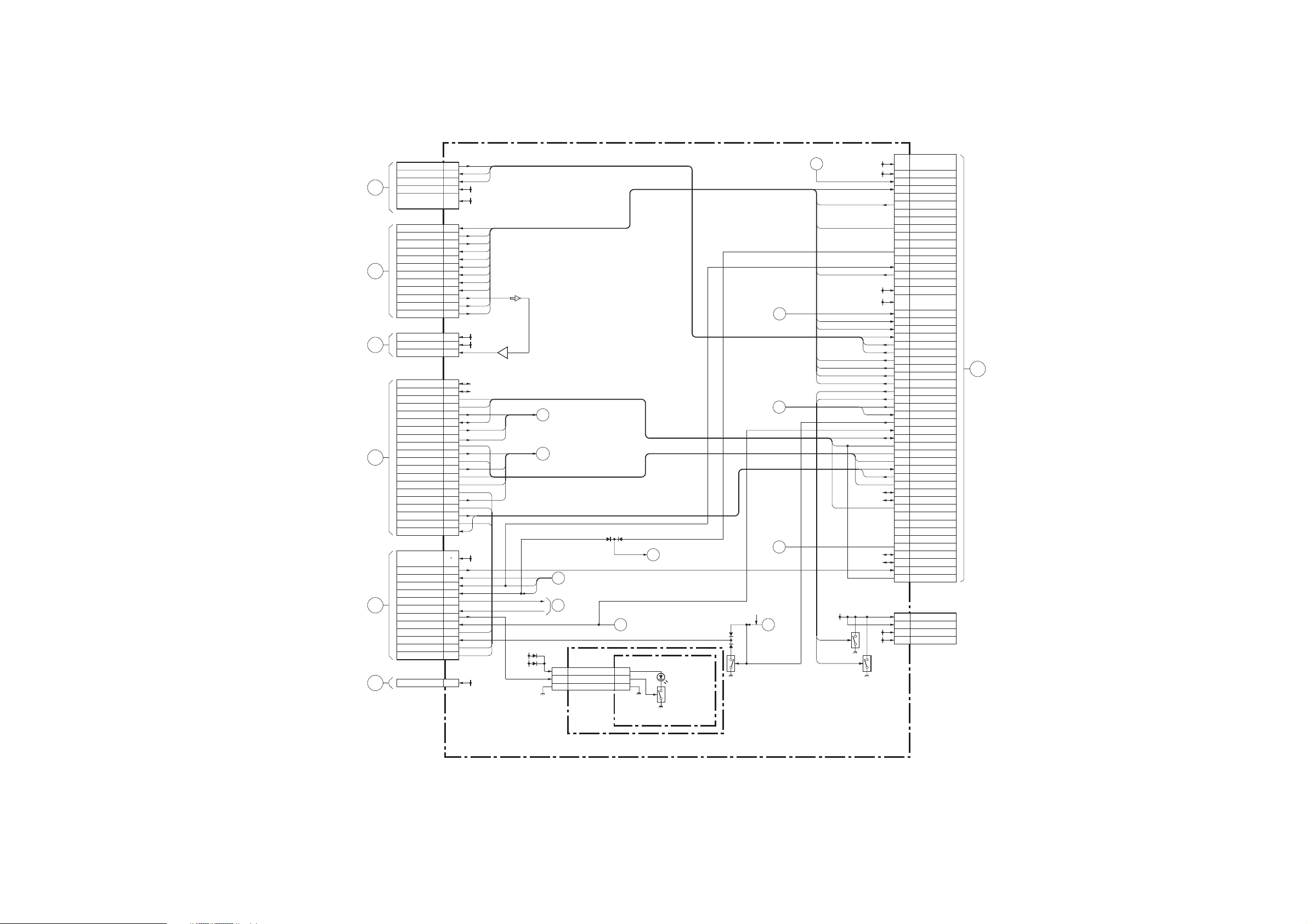
(3) A2FU (2/2) AND H4 BOARDS
M
TO
QM BOARD
CN7300
G
TO
A1U BOARD
CN001
H
TO
K BOARD
CN2600
E
TO
A1U BOARD
CN011
K
TO
DE1 BOARD
CN5203
Y
TO
QT BOARD
CN7902
CN8208
RXD
TXD
RESET
5V
9V
CN8205
HDMI RST
AFT MAIN
TU-H-MAIN
AGC ATT
AD RST
AD MUTE
LINE MUTE
SP MUTE
WOOFER MUTE
SPDIF
SUC C
SUB Y
CN2002
SW5V
SUB11V
SPDIF-
CN8207
I2C SCL
I2C SDA
B INT
AC DET(NC)
USBDPLS
SIRCS
USBDMNS
USBCONNECT
JIG VBUS
UART TRXD1
JIG UDP
UART TRXDP
JIG UDM
UART TXD1
PAN UDM
UART TXDP
PAN UDP
USER TXD
PAN VBUS
USESR RXD
CN8201
SUB6.5V
SYS RESET
THERMO G
FAN ERROR
FAN DRV
PANEL ON
PS PROT
LOGO
D OVP
PAN UDP
SET-ON DE
PAN UDM
PAN VBUS
CN8210
CN8204
A1,A2
TO 1/2
1
2
3
5
ATSC5V
9
ATSC9V
10
1
2
4
6
5
8
9
11
13
15
18
20
1
3
6
3
7
9
10
13
14
15
17
19
20
21
22
23
24
25
26
27
28
29
30
3
6
7
8
9
10
11
12
13
14
15
16
17
18
2ATSC A9V
AUDIOL/R
D5V
11V
I2C-SCL
I2C-SDA
6.5V
ATSC A9V
Q2005
STBY5V
A5V
3
2
CN2003
TO 1/2
TO 1/2
6
5
1
TO 1/2
TO 1/2
THRU5V
TO 1/2
9
TO 1/2
8
TO 1/2
FAN DRIVE
TO 1/2
111
CN1501
1
LOGO
22
33 GND
TO 1/2
6
D1501,1503,1505
D1507,1509,1511
D1513
Q1501-15073
Q2010
11
SET_ON
TO 1/2
7
IFT_BINT
ATSC5V
ANTM
ANTS
Q2012
STBY5V
D5V
ATSC5V
SW3.3V
ISC SDA
I2C-SCL
SDA-1
SCL-1
5V
9V
Q2013
B1
A3-B4
B6
B8
B9
A10
B10
A11
B11
A12
FAN_POW_SW(NC)
B12
TU_H_MAIN(NC)
A13
FAN_SPEED(NC)
B13
TU_H_SUB(NC)
A14
B14
A15
A16
B15,B16
B17,B18
A19
A21
A23
B25
B26
B27
B28
B29
A30
B30
B31
B32
B33
A34
B34
A35
B36
A37
B37
B38
B39
B40
A41
B41
B42
B44
A45
B45
A46
B46
A47
A48
A49
A50
B50
CN8211
1
3
4
5
STBY5V
D5V
+B OVP
AFT_MAIN
FMONO(NC)
AGC_ATT
I_SAP(NC)
O_SAP(NC)
AFT_SUB(NC)
FAN_EROR
AD_RST
AD_MUTE
ATSC5V
SW3.3V
CVY_MAIN
SUB_Y
SUB_C
ATSC_RXD
ATSC_TXD
ATSC_RST
HDMI_RST
LINE_MUTE
SP_MUTE
WOOFER_MUTE
ANT_S
ANT_M
POW_CLT
AC_RLY
SET_ON
D_OVP
SIRCS
SYSTEM_RST
JIG_UDM
JIG_UDP
USER_RXD
USER_TXD
VBUS
I2C_SDA
12C_SCL
B_INT
I2C_SW(NC)
ROM_SDA(NC)
ROM_SCL(NC)
DDC_WE(NC)
IFP_BINT
SDA_1
SCL_1
DE_RST
AC_DET
MS1
MS2
5V
9V
L
TO
M1U BOARD
CN7004
H4
A2FU(2/2)
KDE-37XS955/42XS955 (UC) 3-3
(4) DE1 BOARD
R
TO
DIC3 BOARD
CN4202
K
TO
A2NU(2/2)BOARD
CN8201
U
TO
K BOARD
CN2603
CN5101
SCL_1
SDA_1
IFPFLDOUT
IFPHS
IFPVS
IFPCK
IFPB2OUT0-9
IFPG2OUT0-9
IFPR2OUT0-9
IFPB1OUT0-9
IFPG1OUT0-9
IFPR1OUT0-9
CN5203
SYS_RESET
THERMO_G/3.3V
FAN_ERROR
FAN_DRY 10
PANEL_ON/DAT_D 11
PS_PROT/CLK_D 12
LOGO 13
D_OVP 14
PAN_UDP 15
SET_ON_DE 16
PAN_UDM 17
PAN_VBUS 18
DAT_D 23
CLK_D 24
CH_M/S_SW 25
CH_IIC_SW 26
SP_PROT 27
A_MUTE 28
OF_LAG 29
3.3V_SW 30
CH_WP 31
CH_RST 32
M_RST 33
SCLATCH 34
AMP_RST 35
SCLATCH2 36
SCDT 37
SCSHIFT 38
A1
B1
A3
C3
D3
A4
7
8
9
EXT_SDA
EXT_SCL
IFP_SCL
IFP_SDA
IC5201
SYSTEM
RESET
NC
IFFIELD
IFHSYNC
IFVSYNC
CLK
IFQO0-9
IFQO10-19
IFQO20-29
IFQE0-9
IFQE10-19
IFQE20-29
IC5401
5
6
R
G
B
54
OVHS_P
55
OVVS_P
56
OVBLKDE_P
11
CLKIN
22
RD
IC5203
EEPROM
SDA2A
SCL2A
WP
Q5202
LVDS TRANSMITTER
TA -
TA +
TB -
TB +
TC -
TC +
TCLK -
TCLK +
TD -
TD +
TE -
TE +
TD6
Q5203
IC5302
CPU
OVRED0-9
E26
IFFIELD
A2
IFHSYNC
A3
IFVSYNC
B25
CLK
10
10
10
10
10
10
X5302
33MHz
Q5205
3.3V
AC2
CLKC
ADI
XCLKC
ICSCL
BCSDA
27
SCL0
28
SDA0
64
SCL1
65
SDA1
90
RESET
TEMP1
92
FAN_ERR
69
FAN
93
PANELON
95
ERR2
70
LOGO
74
USB_DVP
73
USB_DVM
71
USB_VBUS
82
CH_M/S_SW
81
CH_IIC_SW
102
SP SPOT
101
AUDIO MUTE
8
OF_FLAGX
6
K3.3V_SW
46
CH_NVM_OP
51
CH_RST
100
AUDIO RESET PRO
9
SCL_LATCH
103
AUDIO RESET AMP
10
SCLATCH2
19
SOT1
20
SCK1
80 HCDHX
IFQO0-29
IFQE0-29
SYSTEM CONTROL
OVGRN0-9
OVBLU0-9
OVHS
OUVS
OVBLKDE
OVCLK
CLX
ICBLK
ICFREE
OFFIELD
IC5202
AC1
AD2
AC3
AF2
F26
E24
G24
K26
FHP_CPUGO
FHP_PDPGO
P_ALARM
D_DEV_RST
PANEL_PD
IC BLK
IC FREE
DEW_DET
NVM_WP1
DEW_DET
BUS_SW0
OVRED1
OVGRN1
OVBLU1
OVHS
OVVS
OVBLKDE
OVCLK
25
INT_V
84
85
83
11
SINO
12
SOTO
17
SCKO
50
55
60
61
104
BINT
21
P60
22
P61
89
MD0
87
MD2
53
67
SDA2
66
SCL2
99 7
44
91
107
XI
108
XO
X5201
6MHz
8
8
8
PANEL_PD
SUB6.5V
Q5208
L5414 - L5419
31
30
29
28
25
24
23
22
21
20
19
18
3
IC5204
65
2
1
3,7
+3.3V
+1.8V
FILTER
EXT_SDA
EXT_SCL
2
2
EXT_SCL
EXT_SDA
FHP_CPUGO
FHP_PDPGO
P_ALARM
IC5210
+3.3V REG
5
IC5207
+1.8V REG
5
FHP_CPUGO
FHP_PDPGO
P_ALARM
JIG_RESET
1
1
SUB6.5V
CN5401
1
TA -
3
TA+
5
TB-
7 TB+
9 TC-
11 TC+
13 TCLK-
15 TCLK+
17 TD-
19 TD+
21 TE-
23 TE+
4 SCL/LVDSGND
8 SDA/LVDSGND
12
CPUG0/GND
PDPG0/GND
14
16 IRQ/GND
18 PWDN/GND
CN5201
SIN
3
SOT
4
5
SCK
RESET6
BINT9
P6010
P6111
M0012
M0213
CN5212
1 WFR_DET
CN5213
1
DEW_DET
3 GND
TO
PANEL
UNIT
TO
WOOFER
SPEAKER
TO
SENSOR
DE1(SYSTEM CONYROL, LVDS TRANSMITTER)
KDE-37XS955/42XS955 (UC) 3-4
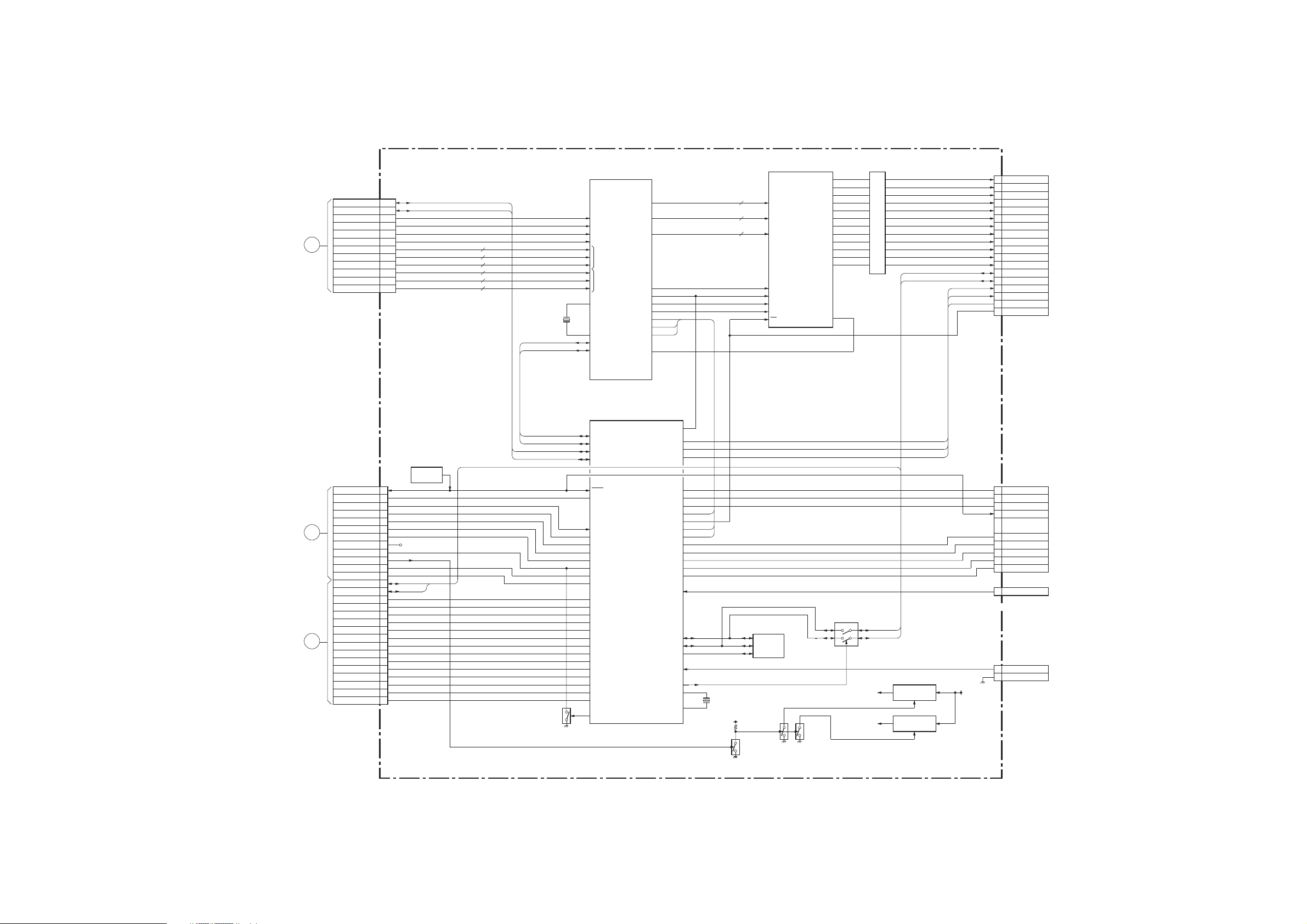
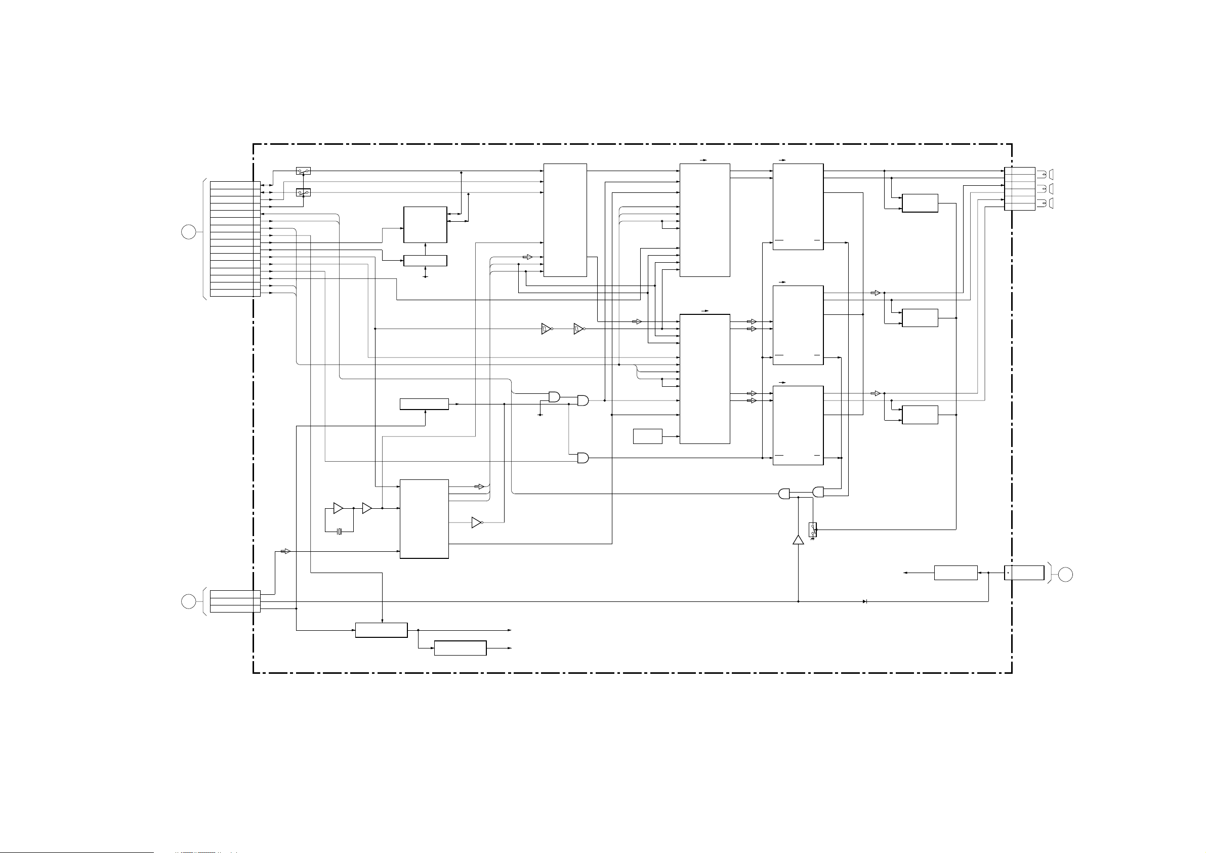
(5) DIC3 BOARD
I
TO
A2FU(1/2)BOARD
CN8203
Q
TO
M1U BOARD
CN7552
S
TO
M1U BOARD
CN7553
CN4000 Q4306,4317
CN4002
CN4003
A1
B2
A3
B3
B4
A5
B5
B6
A7
B7
B8
A9
A11
A12
A14
A15
B15
A17
B17
A18
B18
A19
B20
A21
B21
B22
A31
B10,B11
B12
A13
B14
A24-B25
A27-B28
A30,B30
A33-B34
2
3
4
7
8
9
10
13-16
19-22
25-28
31-34
37
38
39
40
43-46
-
49-50
1,2
5-8
11-14
17-20
23-26
29-32
35-38
41
42
43
45
46
47
48
49
I_BINT
MSDIO
MSCK
I2CMSCL1
D_OVP
I2CMSDA1
M_YS
MSBS
USBCONNECT
USBDMNS
I_BOOTMODE
USBDPLS
I_HDMI_ERR
MSDIR
O_HDMI_RESET
UARTTXD1
UARTTXD2
UARTRXD1
MSPI
UARTRXD2
1
SW2.5V
SW3.3V
SW5V
I_BINT
SW3.3V
1
24
IC4609
3.3V
IC4615
34
61
CCPIN_A(CCPYIN_A0-A7)
CCPIN_A(CCPCIN_A0-A7)
I_GXAIN0_A-I_GXAIN7_A
I_GXGIN0_A-I_GXGIN7_A
I_GXBIN0_A-I_GXBIN7_A
I_GXRIN0_A-I_GXRIN7_A
Q4009,4012
SW3.3V
IC4002
I2C_SDA
I2C_SCL
I2C_MSCL1
I2C_MSDA1
I_MAIN_C
B_INT
I_MAIN_CV
O_MSDIO(NC)
I_MSLK(NC)
I_MAIN_R
SET_ON
CLK_W
I_MAIN_B
D_OVP
DAT_W
I_MAIN_G
I_MAIN_YS(NC)
O_MSBS(NC)
I_USBCONNECT
I_USBDMNS
BOOT_MODE
I_USBDPLS
HDMI_ERR(NC)
O_MSDIR(NC)
HDMI_RESET(NC)
I_UARTTXD1(NC)
I_UARTTXDP
I_UARTRXD1(NC)
O_MSPI(NC)
I_UARTRXDP
SYSTEM_RESETX
D_1.8V(NC)
D_1.2V(NC)
D_1.25V(NC)
A_1.8V(NC)
SW_2.5V
SW_3.3V
SW_5V
SUB_6.5V
O_IFPVSOUT
O_IGXHSOUT
O_IGXCKOUT
I_GXYCCKIN
I_GXYCHSIN
I_GXYCVSIN
O_PCCOSOUT
I_GXYIN 0-7
I_GXCIN 0-7
I_GXCKIN
I_GXHSIN
I_GXVSIN
O_PCCLPOUT
I_GXAIN 0-5
I_GXAIN 6,7
I_GXGIN 0-7
I_GXBIN 0-7
I_GXRIN 0-7
CLK_M
DAT_M
M/S_SW
OSDV_M
PC_HPOL
PC_VPOL
OSDH_M
CCPM_MUTE
Q4305,4316
Q4304,4314
Q4303,4313
Q4302,4312
IC4000
1,2
1.2V
7
ENA
IC4001
1,2
1.8V
7
ENA
1.8V
399
MSDIO
MSCK
MSBS 290
USBCONNECT 495
USBMNS 42
USBDPLS 168
Q4016
173
S4600
IC4614
43
16
16
6
3
4
7
Q4006,
8
8
8
8
Q4007
501
175
594
593
500
489
141
260
247
463
359
474
243
122
459
371
497
396
276
490
161
SW3.3V
UARTRXD2
UARTRXD1
UARTTXD2
UARTTXD1
MSPI
MSDIR
I_HDMI_ERR 393
O_HDMI_RESET
I_BOOTMODE 158
2
1
I2C_SCL SCL
I2C_SDA SDA
14,15
REG
13
14,15
REG
13
REG
IC4610(1/2)
MSDIO
49
MSCK
MSBS
USBCONNECT
USBMNS
USBDPLS
MSPO
40
GPIO_INT0
UARTRXD2
UARTRXD1
UARTTXD2
50
UARTTXD1
MSPI
MSDIR
GPIO_INT1
GPIO8
GPIO15
EXTGXHSOUT
EXTGXCKOUT
CCPCKIN_A
CCPHSIN_A
CCPVSIN_A
PCCOSOUT
I_GXYIN0-A
I_GXYIN7-A
I_GXCIN0-A
I_GXCIN7-A
EXTGXCKIN
EXTGXHSIN
EXTGXVSIN
PCCLPOUT
I2CSSCL2
I2CSSDA2
GPIO14
35
GPIO4
GPIO5
GIPO2
IC4302
VIDEO BUFFER
11
IN2A
8
IN1A
3
SDAI2C_SDA
4
IC4303
VIDEO BUFFER
13
IN3A
11
IN2A
8
IN1A
3
4
SCLI2C_SCL
Q4000
Q4001IC4301
3,14,16 2
FP
GPIO7
DRCHSIN
Q4310
21
OUT2A
20
OUT2B
25
OUT1A
24
OUT1B
OUT3A
OUT3B
OUT2A
OUT2B
OUT1A
OUT1B
Q4309
17
16
21
20
25
24
IC4305
Q4300,4307
OP AMP
14
INC+ AOUT2
Q4301,4308
5
INA+
7
OUTA
16
OUTC
IC4803
1.25V
6
REG
278
252
563
4
IC4304
SDRAM
1.8V
167
FL4300
L.P.F
FL4301
L.P.F
3.3V
2.5V
199
196
262
106
DQ 0-15
16
ADDR 0-11
12
DQM,BA0,BA1
3
XCS,XCAS,XWE
33XRAS,CKE,SOCLK
197
15
AIN5
13
AIN4
20
AD4 SEL
11
AIN3
AIN2
9
AIN1
69
67
AOUT1
66
FIFOCLK_IN
70
DTOCLK_IN
HDD
VDDDRCVSIN
CK2CQCCPYIN_B0
FIM0
OSDV
46
OSDH
IC4300
OCPX
-
-
7
90
4
28
44
MAIN_D2IN
(M_D2C 2-9)
8
MAIN_D2IN
(M_D2Y 2-9)
8
(M_D2H)
(M_D2V)
(M_D2CLK)
Q4200
1MAIN_CCPYUV
(1MY 2-9)
1MAIN_CCPYUV
(1MC 2-9)
1MAIN_CCPYUV
(1M_CLK/HS/VS)
(1M_CLK/HS/VS)
IC4503
SDRAM
IC4504
SDRAM
IC4004
2
4
1
D2C
D2Y
D9Y RD8
HTIM
VTIM
CLK
XRST
OSDY
IC4202
POWER
ON
RESET
3.3V
(1MY 2-9)
8
(1MC 2-9)
8
3
D0_0-31
32
A0_0-10
10
CK0,CS0,WE0
CAS0,RAS0
B0_0_1
D1_0-31
32
A1_0-10
10
CK1,CS1,WE1
CAS1,RAS1
B1_0_1
IC4200
LVDS RECEIVER
RA1
RA8D9C
RD1
--
21
RD0
14
RD6
RCLK-
RCLK+
31
CLKOUT
3
PD
8
8
3
IC4505
DRC MFV1
DIYD0
DIYD7
DICD0
--
DICD7
3
2
2
3
2
2
49
RA-
50
RA+
51
RB-
52
RB+
56
57
59
RD-
60
RD+
DRCIN
DB02
(DRCC1IN 0-7)
-
DB09
DRCIN
DR02
(DRCC2IN 0-7)
-
DR09
DY212
DY219
DY202
DY209
DRCIN
(DRCY1IN 0-7)
DRCIN
(DRCY2IN 0-7)
-
IC4502
4
297
XRST
132
7
PLL CLK GEN.
7129
CLKI SSCLK
CN4200
1
MRXIN0-
2
MRXIN0+
MRXIN1-
4
MRXIN1+
5
MRXIN2-
7
8
MRXIN2+
10
MRXCLK-
11
MRXCLK+
13
MRXIN3-
14
MRXIN3+
8
8
8
8
2
124
IC4604
IC4506
PLL CLK GEN. PLL CLK GEN.
3
SSCLK
XINCKBI
8
SSON
IC4507
8
SSON
13
XIN
IC4508
7
CLKD S1
9
CLKB
IC4801
ROM
DQ0
-
DQ7
A0-A20
DQ15,A-1
S1
XIN
79.99MHz
13
12
4
X4500
WE,OE,CE
IC4610(2/2)
D0-D7
8
A0-A21
22
FP
IC4600
PLL CLK GEN.
47
TALCLKIN GPIO10
X4600
79.99MHz
GPIO6
587
GPIO_INT3
36
279
388
GPIO0
GPIO3
GPIO6
GPIO11
GPIO12
386
488
IC4608
IC4611
IC4613
VOLTAGE
DETECTOR
6.5V 5V 2.5V
CLKC
4
XIN
IC4603
PLL CLK GEN.
8
SSON
SYSTEM RESET
3
24
1
-
71
S1
S0
CLKB
XIN
IC4601
CK
RTC
VS
IC4602
RESET
1
DDR MEMORY
32
12
ROM_WE/OE/CS1
MCLK1
MCLK1B
MCLK0
MCLK0B
AJ10GPIO
MCSB0
MRASB
MCASB
MMEB
MMD0-63
MMA0-11
MMBA0-MMBA1
2
MDQS0-MDQS7
8
MDQM0-MDQM7
8
204
81
205
82
494
201
317
78
614
13
12
9
3
7
42
1
IC4800
IC4802
9
I2CMSCLK1
372
IFPFLDOUT
142
IFPMSK1OUT
140
IFPHSOUT
13
IFPVSOUT
569
IFPCKOUT
277
387
GPIO9
PNLCLKINSSCLK
345
8
RESETX
48
STANDBYX
340
ARM_TDO
543
ARM_TCK
632
ARM_TRST
105
ARM_TDI
227
ARM_TMS
I2CMSDA1
61
IC4614
IFPR1OUT 0-9
IFPG1OUT 0-9
IFPB1OUT 0-9
IFPR2OUT 0-9
IFPG2OUT 0-9
IFPB2OUT 0-9
A1
B1
A3
B3
C3
D3
A4
B25
C28
10
C21
A25
10
C16
B21
10
A13
B16
10
A9
C12
10
B4
D7
10
6
5
4
3
2
DIC3
(LVDS RECEIVER,FP,CCPX,DRC MF)
CN4202
CLK_W
DAT_W
IFPFLDOUT
IFPMSK1OUT
IFPHS
IFPVS
IFPCK
IFPR1OUT 0-9
IFPG1OUT 0-9
IFPB1OUT 0-9
IFPR2OUT 0-9
IFPG2OUT 0-9
IFPB2OUT 0-9
CN4600
TDO
TCK
TRST
TDI
TMS
R
TO
DE1 BOARD
CN5101
KDE-37XS955/42XS955 (UC) 3-5
(6) F AND G1 BOARDS
TO
AC INLET
AC IN
CN6001
AC(N)
AC(L)
1
2
F
F6001
L6002-6005
CN6018
2
1
AC(N)
AC(L)
CN6014
2
1
RY6001
Q6915
STBY5V
RY6002
Q6903
RLY5V
PH6904
Q6201,6202
PROTECT
D6100
IC6202
DRIVE
6
CAOUT
8
AC OFF
TH6101
D6106
Q6217
D6201,
6225 6226
16
OUT
15
VCC
9
VREF
3
13
SS
11
VFB
RV6201
Q6209
D6103
2
5
D6205
D6208,
Q6203,Q6205
PFC DRIVE
IC6101
DRIVER
VCC
START UP
RECT
DRAIN
DRAIN
D6216
L6201,L6203
Q6210
SS
Q6212
Q6213
D6218
LATCH
7
8
4
FB
D6217
Q6206,6207,6219
PFC SW
IC6201
12V REG
VCC
3
OUT
CTL
Q6214
OVP
Q6208
IC6204
VREF
Q6211
LVP
Q6204
SS
PH6101
2
1
8
6
4
3
T6101
D6104
CN6017
1
PFC_DET
3
PRI_VCC1
5
PFC_OUT
PRI_GND
2
RLY5V
STBY5V
1
2
12
13
10
11
10
Q6215
Q6216
LATCH
IC6203
PROTECT
3
2
5
6
9
D6105
14
1
7
8
Q6218
PH6905
STBY5V
CN6901
RLY_5V
31RLY_ON
P_SW(-)
5
STBY5V
6
W
TO
G2F BOARD
CN6010
X
TO
G2F BOARD
CN6301
IC6102
VREF
(POWER SUPPLY)G1
KDE-37XS955/42XS955 (UC) 3-6
(7) G2F BOARD
W
TO
G1 BOARD
CN6017
X
TO
G1 BOARD
CN6901
CN6010
PFC DET
PRI VCC
PFC OUT
CN6301
RLY 5V
RLY ON
P-SW(-)
STBY 5V
T6301
IC6301
DRIVER
15
VC1
Q6502
SW
D6501
1
VSENSE
VC1
2
F/B
2
1
VSENSE
15
VC1
2
F/B
IC6701
DRIVER
VG(H)
VG(L)
F/B
D6310
IC6501
DRIVER
VS
OCP
VC2
Q6702
SW2
D6301
15
D6700
1
2
5
1
3
5
6
VG(H)
VG(L)
23
22
20
16
17
VG(H)
VG(L)
VS
OCP
D6702
OCP
VS
23
22
20
16
23
22
20
16
Q6703
Q6704
Q6301
CONVERTER
Q6302
CONVERTER
D6308
PH6401
ISOLATER
PH6902
ISOLATER
Q6901
Q6503
CONVERTER
Q6514
CONVERTER
PH6601
ISOLATER
PH6903
ISOLATER
Q6705
CONVERTER
Q6706
CONVERTER
PH6801
ISOLATER
SUB11V
IC6405
VREF
IC6408
DC-DC CONV.
SUB11V
T6501
PIT D6601
3
6
SUB11V
T6701
PIT
3
6
T6702
PIT
3
6
SUB11V
2
4
6
7
OUT2 U
OUT2 D
SBY 2
15
12
10
15
10
15
10
PIT
17
19
10
D6911
LATCH
14
10
13
11
16
15
9
Q6411
Q6412
D6801
D6804
D6406
D6408
D6407,D6417
D6403
Q6405
D6402
D6405
D6404
VCC
5V
Q6409
Q6410
D6418
SUB11V
D6908
D6810
Q6801
Q6802
D6409
Q6406
D6401
IC6901 OVP,LVP
7
1
6
10
13
11
4
2
5
Q6916
Q6917
LATCH
D6912
Q6909,Q6912
9
8
VCC5V
IC6902
V REF
RV6801
VA_ADJ
IC6407
REG
14
Q6805
LATCH
1
Q6905
Q6913
IC6403
3
FAN
4
DRIVE
IC6402
5V
REG
Q6902
Q6910
LATCH
IC6404
RLY_ON
IC6802(1/2)BUFF
12
13
2
3
LATCH
14
6804
1
Q6908
Q6907
9
8
10
5
7
6
IC6802(2/2)
CONTROL
SUB11V
Q6407
Q6408
IC6401
21
9V REG
4
4
13
VCC5V
Q6914
SW
IC6801
VREF
RV6802
VS_ADJ
8-10
3.4
1.4
7.10
2
5
8
11
1.4.7
2
5
8
1
3
5.6
1.2 AUDIO25V
1
3
4
6
7
8
9
11
12
13
TH6403
1
3
5
6
7
8
1
3
8
9
10
CN6008
SUB11V
SUB6.5V
CN6006
FAN
FAN ERR
FAN ERR
FAN ERR
FAN ERR
CN6021
FAN
FAN ERR
FAN ERR
FAN ERR
CN6009
SUB18V
THRU5V
SW9V
CN6005
CN6004
TU32V
AC RLY
P-SW(-)
STBY5V
OVP
PS PROT
REC ON
FAN ERR
FAN DRVIVE
THERMO
CN6007
VCC5V
VPR2
VRA
VRS
VCEGO
VSAGO
CN6013
VA
VCC5V
VS
VS
VS
J
TO
A2FU(1/2)BOARD
CN2001
TO
FAN
TO
FAN
F
TO
A2FU(1/2)BOARD
CN2004
V
TO
K BOARD
CN2602
C
TO
A2FU(1/2)BOARD
CN2005
TO
PANEL
UNIT
TO
PANEL
UNIT
G2F
(POWER)
KDE-37XS955/42XS955 (UC) 3-7
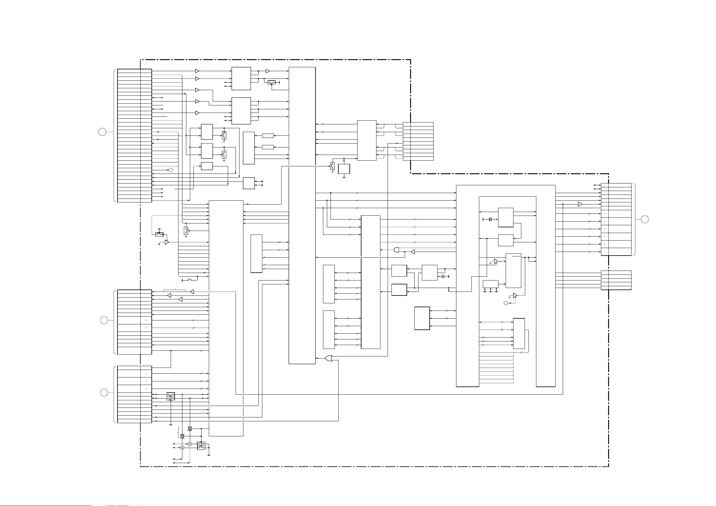
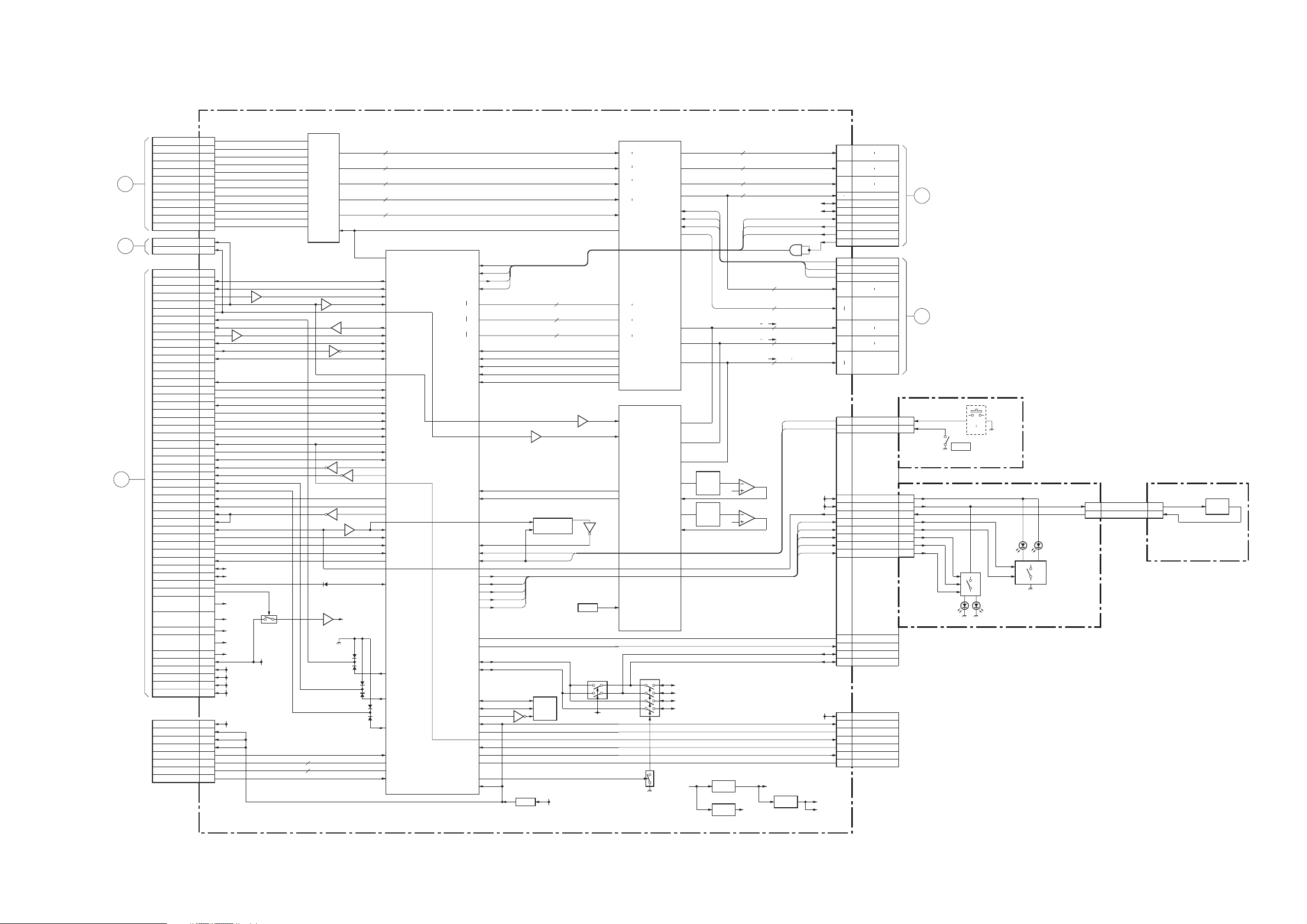
(8) K BOARD
U
TO
DE1 BOARD
CN5203
H
TO
A2FU(2/2)BOARD
CN2002
CN2603
DAT_D
SLK_D
CH_M/S_SW
CH_IIC_SW
SP_PRT
A_MUTE
OF_FLAG
3.3V_SW
CH_WP
CH_RST
M_RST
SCLTCH
AMP_RST 15
SCLTCH2 16
SCDT 17
SCSHIFT 18
CN2600
SPDIF-
SUB11V
5V
3
4
5
6
7
8
OF_FLAG
9
10
11
12
13
14
SCDT
SSCHIFT
AUDIO L/R
6
3
1
IC2611
4
1
3
18
2
5
SP_PRT
A_MUTE
IC2610
EEPROM
SDA
7
VCCDET
XMODE(I) DATA(O)
IC2612
X2600
24.576MHz
13
22
3
2
IC6103
+3.3V REG
XIN(I)
DION(I)
SCL
NP7
VCC
Q2610,Q2611
CH RESET
3.3V
IC2602
RESET
DELAY
IC2600
CONT.SIG.GEN.
LRCK(O)
BLK(O)
ERROR(O)
CKOUT(O)
+1.8V REG
5
6
1
AUDIO L/R
1648
15
14
34
13
IC6102
Q2602
DATA(O)
LRCK(O)
BCK(O)
45
IC2603
DIGITAL AUDIO PROCESSOR
12
I2C_SDA
27
I2CM_S
13
I2C_SCL
9
A_MUTE
SP_PRT
+3.3V
+1.8V
MCLKI
14
SDIN1
38
LRCLK
1
SCLKIN
IC2609
1
75
IC2601(2/2)
2
3
1
3.3V
AUDIO L/R
SDOUT2
SDOUT1
3
4
5
IC2614
2
1
IC2607
32
SCDT
SCSHIFT
OF_FLAG
30
AUDIO L/R
SCDT
SCSHIFT
OF_FLAG
6
X2601
49.152MHz
4
12S PWM
31
DATA OUTL1
19
SOFMUTE
36
XFSIN
21
SCDT
22
SCSHIFT
24
OVFFLAGR
25
OVFFLAGL
23
SCLATCH
29
LRCK
30
BCK
27
INIT
IC2604
12S PWM
31
27
INIT OUTL2
30
BCK
29
LRCK
23
SCLATCH
21
SCDT
22
SCSHIFT
24
OVFFLAGR
25
OVFFLAGL
19
SOFMUTE
36
XFSIN
48
XFSOIN
11
9
OUTL2
AUDIO R
11
OUTL1DATA
9
AUDIO L
6
OUTR1
4
OUTR2
K
(AUDIO PROCESSOR,AUDIO DRIVE)
IC2608
PWM WOOFFER DRIVE
2
17
PWN_AP OUT_A
4
RST
IC2606
PWM AUDIO LCH DRIVE
2
PWN_BP
17
PWN_AP
4
RST
IC2605
PWM AUDIO RCH DRIVE
2
17
PWN_AP OUT_A
4
RST
IC2601(1/2)
10
8
9
Q6101
Q6102
OUT_BPWN_BP
DREG
SD
OUT_B
OUT_A
DREG
SD
OUT_BPWN_BP
DREG
SD
5
30
25
8
13
30
25
8
13
30
25
8
13
12
13
Q2603
AURIO R
AURIO R
D6101
W+
W-
L+
L-
R+
R-
+12V
Q2608,Q2609
DC
DETECT
Q2605,Q2607
DC
DETECT
Q2604,Q2606
DC
DETECT
IC6101
+12V REG
CN2601
1
W+
2
W-
3
L+
4
L-
5
R+
6
R-
CN2602
1
AUDIO_VCC
2
WOOFFER
L
R
V
TO
G2F BOARD
CN6005
KDE-37XS955/42XS955 (UC) 3-8
(9) H1U, H3, H5 AND M1U BOARDS
CN7650
T
TO
QM BOARD
CN7304
AA
TO
A1U BOARD
CN301
L
TO
A2FU(2/2)BOARD
CN8204
GRA -
GRA +
GRB -
GRB +
GRC -
GRC +
GRCLK -
GRCLK +
GRD -
GRD +
GRE -
GRE +
SUB Y
SUB C
REC ATT
D SAP
AD MUTE
CVY MAIN
SUB Y
SUB C
SP MUTE
AC RLY
D OVP
SYSTEM RST
V BUS
IFP BINT
I2CMSDA1(NC)
I2CMSCL1(NC)
DE RST
+B OVP
AFT MAIN
FMONO
I SAP
AFT SUB
TU H MAIN
TU H SUB
AD RST
ATSC RXD
ATSC TXD
ATSC RST
HDMI RST
LINE MUTE
WOOFER MUTE
ANT S
ANT M
POW CTL
SET ON
SIRCS
JIG UDM
JIG UDP
USER RXD
USER TXD
I2C SDA
I2C SLK
B INT
AC DET
STBY 5V
ATSC 5V
SW3.3V
SW9V
STBY 3.3V
STBY 2.5V
DIC A 1.8V
DIC D 1.8V
ADC 3.3V
UVCC
XTRST
XRSTIN
CINIT
DPEAK
ICD 0-3
ICS 0-2
ICLK
CN7005
CN7004
D5
CN7001
1
2
4
5
7
8
10
11
13
14
16
17
A10
A11
A15
A19
A21
A23
A30
A34
A35
A37
A41
A47
A48
A49
A50
B6
B8
B9
B10
B11
B12
B13
B14
B25
B26
B27
B28
B29
B30
B31
B32
B33
B34
B36
B37
B38
B39
B40
B41
I2C SDA-X
B42
I2C SCL-X
B44
B50
A1,A2
STBY5V
B1
A3,A4
SW5V
B3,B4
A16
ATSC5V
B15,B16
SW3.3V
B17,B18
A52
SW9V
A56
STBY2.5V
A57
DIC A1.8V
A58
DIC D1.8V
A59
ADC 3.3V
A60
STBY3.3V
1
2
3
4
5
6-9
10-12
14
M1U
Q7026,7027,7036
Q7005,7008,7007,7038
Q7018
ICD 0-3
ICS 0-2
(MAIN DIN,MPU)
STBY3.3V
IC7650
MAIN DIN
49
RA-
50
RA+
51
RB-
52
RB+
54
RC-
55
RC+
56
RCLK-
57
RCLK+
59
RD-
60
RD+
61
RE-
62
RE+
Q7710,7714
4
3
17-22
24-25 GR 0-7
26-29
36,45
7,8
46,47,31
3
PD
Q7028,7029,7037
Q7009
Q7006
Q7003
Q7604
Q7012
Q7015,2017
Q7025
NC
D7006
D7004
D7011
8
GG 0-732,33-35
8
GB 0-738-43
8
GA 0-710-15
8
GVS,GHS,GSK
3
45
125
O SAP
146
O AD MUTE
29
DATA SLICER MAIN
30
DATA SLICER SUB
76
O AC RLY
126
I DOVP
47
O PTE RESET
136
I VSD DET
52
O PF BINT
49
O DERST
127
I ATSC OVP
39
I AFTMAIN
53
O FMONO
121
I SAP
40
I AFTSUB
89
I MAIN H1H
90
I SUB H1H
50
O AD RST/O MS RST
111
I RXD ATSC
112
I TXD ATSC
142
O ATSC RST
141
O HDMI RST
55
O ANT S
54
O ANT M
79
POW CTL
86
I SIRCS
159
UDM
160
UDP
130
I USER RXD
131
O USER TXD
44
I BINTN
143
O SP MUTE
147
O LMUTE2
145
O SPWFR MUTE
83
I_DPEAK
67-70
ICD 0-3
64-66
ICS 0-2
22
ICLK
IC7002
SYSTEM UC
MASTER WAIT
I POWER LED
O PICCFF LED
O TIMER LED
O POWER LED
LAMP ERR LED
O ISTBY LED
BUS SW-RST
I IFP BUSY
I CCD MV
I CCD MH
D R0
D R2
D G0
D G2
D B0
D B7
YMOUT
YSOUT
DOT CLK
VSYNC
OSDHSYNC
I CODSV
SUB HSYNC
KEY WAKE
I KEY1
PCSTBY LED
O STBY LED
IO SDAT
IO SCLK
IO SDAT
IO SCLK
O_NVMPR
TRSTX
MD2
SI0
SD0
SCK0
O BUS SW
I RESET
85
88
101
87
171
172
175
176
1
99
3
91
37
104
149
146
119
120
117
153
118
110
108
109
107
106
61
73
80
81
82
48
75
5
6
7
Q7019
IC7003
RESET STBY3.3V
PSD R5-R7
3
OSD G5-G7
3
OSD B5-B7
3
OSD YM
OSD YS
DOT CLK I
Q7708,7713
Q7704,7709,7715
Q7022,7024
AMP
79.99MHz
IC7004
NVM
DAT
CLK
WP
54
13
15
Q7002
X7950
217
XTAL
Q7011,7013
BUS LINE SW
STBY3.3V
IC7551
MPU
IGPX1-R0
IGPX1-R7
IGPX1-G0
IGPX1-G7
IGPX1-B0
IGPX1-B7
IGPX1-A0
IGPX1-A7
IGPX1VS/HS/CK
OGPX_HS/VS/CK
RST
IGPX0-R5
IGPX0-R7
IGPX0-G5
IGPX0-G7
IGPX0-B5
IGPX0-B7
IGPX0-A6
IGPX0-A7
OEX CK
OEX VS
OEX HS
IC7701
CCPX
AIN4
AIN5
OSD V
OSD H
PEF CLKIN
IC7005
11
9
1
3
OGPX_R0-R7
8
OGPX_G0-G7
8
OGPX_B0-B7
8
OGPX_A6,A7
2
IEX HS
IEX VS
IEX CK
Q7700
69
AOUT2
DT0CLKIN
AOUT1
FIF0CLKIN
10
8
2
4
Q7020
Q7702
FL7700
70
Q7701
67
Q7703
FL7701
66
I2C SCL X
I2C SDA X
SDAT
SCLK
STBY5V STBY3.3V
IC7001
IC7000
MASTER WAIT
IFP BUSY
CCDV M
CCDH M
OGPX_HS/VS/CK
1SC2-1 9 OPC BE0-7
1SY2-1 9 OPC GE0-7
1S-CLK/HS/VS OPC CK/HS/VS
IC7702
14
16
15
5
7
6
3.3V
REG
2.5V
STBY2.5V
REG
IC7552
4
OGPX_A0-A5
6
3
8
8
3
IC7700
1.8V
REG
I2C SCLX
I2C SDAX
1
2
SW5V
STBY5V
I2C SDAS
I2C SLKS
STBY3.3V
29-32
35-38
5-8
11-14
17-20
23-26
1 2
41
42
43
44
45
48
2
3
4
43-46
49,50
37
39
13-16
19-22
25-28
31-34
7
9
CN7003
4
6
9
10
11
12
13
14
15
16
19 LAMP ERR LED
21
26
25
1
2
3
4
6
7
8
DIC A1.8V
DIC D1.8V
CN7553
O GXRIN0
O GXRIN7
O GXGIN0
O GXGIN7
O GXBIN0
O GXBIN7
O GXAIN6,7
O I2CSSCL2
O I2CS SDA2
M/S SW
IFP BUSY
OSDV M
OSDH M
CN7552
I IFPVSOUT
I IGXHSOUT
I IGXCKOUT
O GXAIN0
O GXAINS
O GXCKIN
O GXHSIN
O GXVSIN
O GXYIN0
O GXYIN7
O GXCIN0
O GXCIN7
O GXYCKIN
O GXYCHSIN
O GXYCVSIN
KEY1
P ON
SW5V/THRU
STBY5V
SIRCS
PCSTBY LED
PICOFF LED
TIMER LED
STBY LED
POWER LED
ILINK LED
SCL
SDA
CN7002
STBY3.3V
RESET
MD2
BUSY3
SI0
SO0
CLK K0
S
TO
DIC3 BOARD
CN4003
Q
TO
DIC3 BOARD
CN4002
CN1051
4
6
CN1200
1
1
2
2
3
3
5
5
6
6
7
7
8
8
9
9
D1205
S1056
POWER
S1051
S1055
H1U
D1203
Q1201
Q1204
Q1205
Q1207
D1206
D1204
Q1203
Q1206
CN1201
H3
STBY5V
1
SIRCS
2
CN1601
1
2
IC1601
SIRCS
H5
KDE-37XS955/42XS955 (UC) 3-9
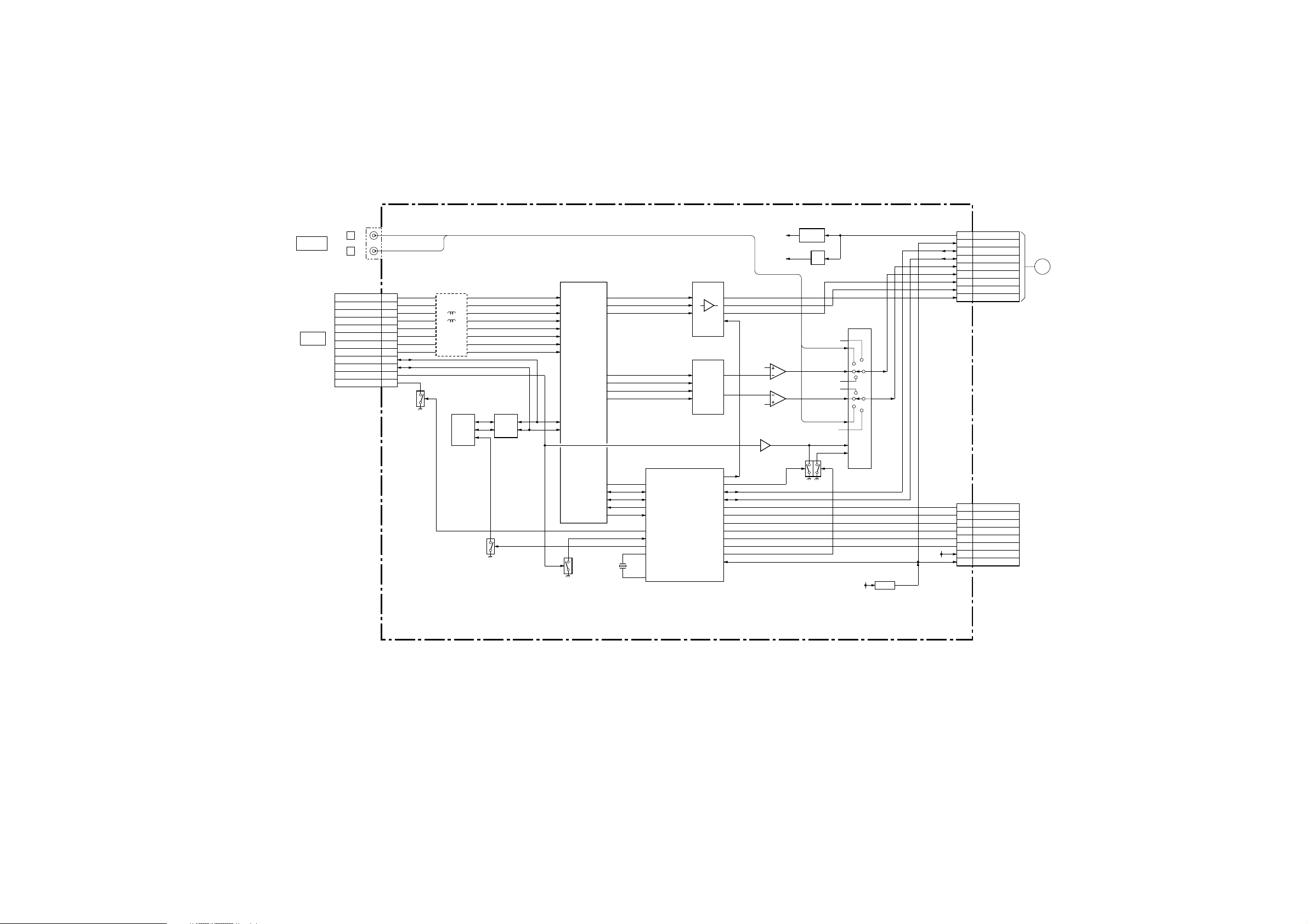
(10) P BOARD
HDMI
AUDIO
HDMI
PC
J9503
L
R
CN9500
D2+
D2-
D1+
D1-
D0+
D0-
CLK+
CLK-
DDC CLK
DDC DAT
DDC +5V
HPD
+5V
IC9514
LPF
Q9511
1
7
IC9503
3.3V
DD CONV.
IC9521
5V
REG
L
R
Q9502
12
14
15
11
4
2
5
1
9
10
IC9506
SW
B
A
+3.3V
13
3
IC9522
5
RESET
+3.3V
4
L
R
4
6
2
AUDIO DAC
2
SCK
3
LRCK
1
SDAT
4
MCLK
IC9517
SUB MICRO
IO-SCL-TV
IO-SDA-TV
REESET-N
IC9500
BUFFER
FSEL
IC9502
O-FCSW
O-ASW2
O-ASW1
12
11
13
16
8
L
5
R
14
22
21
20
36
35
33
32
31
25
11
5
IC9505
FL9501
Q9516
MUTE
FL9504-9506
IC9504
EDID NVM
SCL
SDA
WP
6
5
7
Q9517
IC9509
LEVEL
SHIFT
1
3
4
6
7
9
10
12
15
16
18
19
HDMI RECEIVER
97
RX2+
96
RX2-
92
RX1+
91
RX1-
87
RX0+
86
RX0-
84
RXC+
83
RXC-
76
DSCL
77
DSDA
Q9514
ANGY
ANBPB
ANRPR
SCK
WS
SDO
MCLKOUT
V
CSCL
CSDA
RESET
12
15
7
32
31
30
26
74
75
72
71
X9501
10MHz
Y
PB
PR
27,2834
37
38
24
43
19
41
34
8
9
IO-SCL1
IO-SDA1
O-RESET1-N
I-FMT1
O-HPGMUTE2
I-HPGDET1-N
OSC2
OSC1
+3.3V
3
2
6
5
Q9503,9506
1
2
3
4
6
7
9
11
13
1
2
3
4
5
6
7
8
CN9504
9V
RESET
SCLK
SDAT
PR
PB
CN9505
DEBUG1
DEBUG2
P87
P86
P85
NMI
VCC 3.3V
RESET
R
L
Y
A
TO
A1U BOARD
CN002
P(HDMI)
KDE-37XS955/42XS955 (UC) 3-10
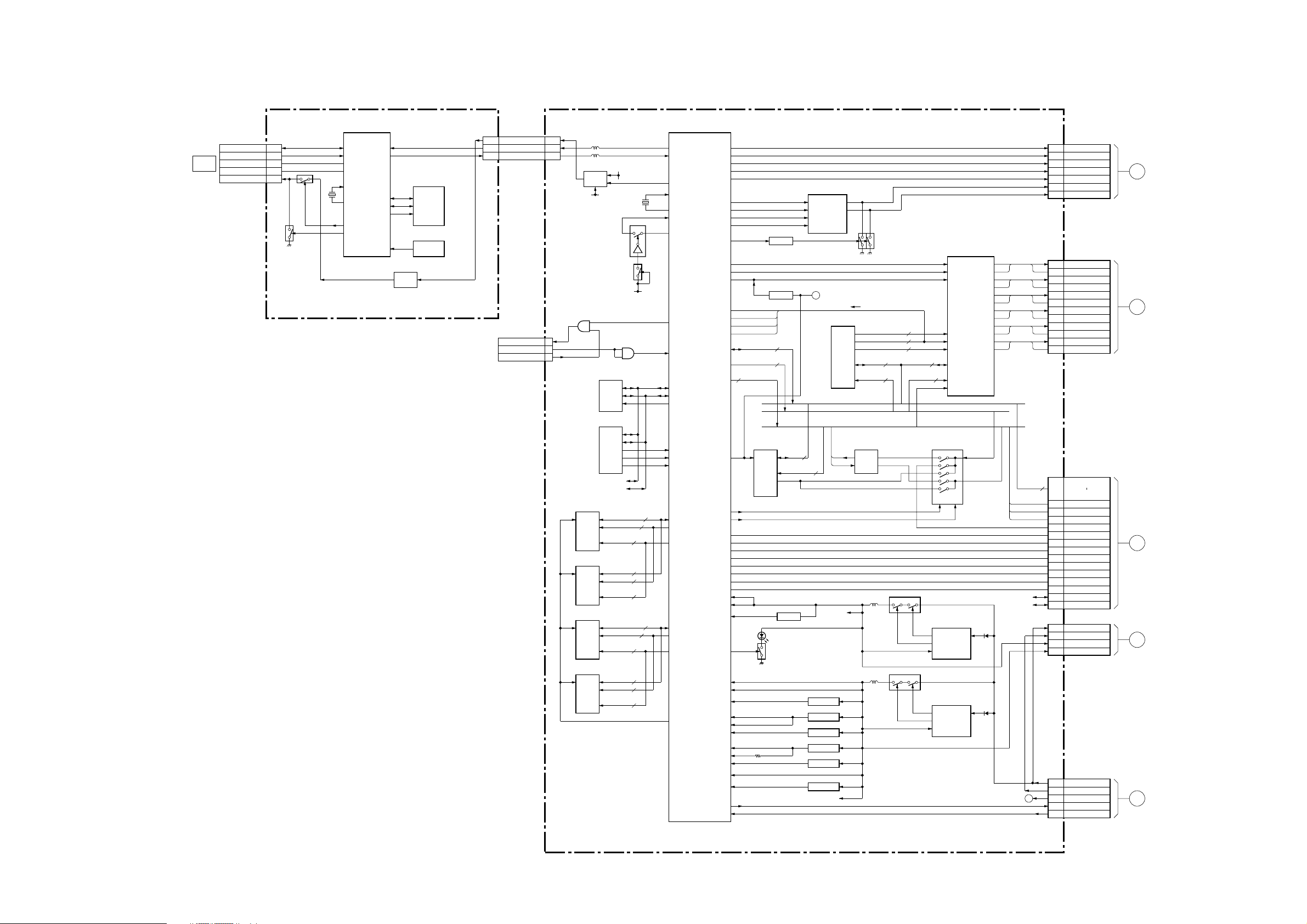
(11) QH AND QM BOARDS
MEMORY
STICK
CN7204
BS
DATA0
INS
SCLK
VDD
2
4
6
8
9
QH
IC7202
MS USB
Q7202
Q7201
X7201
48MHz
19
43
31
42
52
53
29
30
BS0
DATA0
SCLK0
SCLK
XIN
XOUT
ON1
LED
VM
VP
SDA
SCL
WP
RESET
46
45
39 6
27 7
IC7201
3.3V
LDO
540
457
IC7203
EEPROM
SDA
SCL
WP
IC7204
RESET
(MEMORY STICK)
CN7201
2
3
TEST
CONNECTOR
VCC/VBUS
D-
D+
CN7303
TXDB
RXDB
3.3VIN
CN7311
11
2
3
1
2
4
FL7300
IC7330
PWR CTL
D3.3V
IC7335
4
IC7325
DDR SDRAM
49
VREF
IC7323
DDR SDRAM
49
VREF
IC7324
DDR SDRAM
49
VREF
IC7322
DDR SDRAM
49
VREF
USB
5
4
26.1621MHz
1
2
IC7326
EEPORM
SCL
SDA
XWC
IC7321
GFX PLL
SCL
SDA
HSO
VSO
CLK
I2CA_SCL
I2CA_SDA
D0-D7
D24-D31
A0-A14
/WE,/CAS,CKE
/RAS,/CSO
D8-D23
D0-D7
D24-D31
A0-A14
/WE,/CAS,CKE
/RAS,/CSO
D8-D23
MEM_VREF
D5V
X7300
IC7315
42
1
Q7308
D3.3V
IC7336
1
4
2
6 547
5
7
3
2
11
14
12
16
15
5
16
15
5
16
15
5
16
15
5
526
555
556
515
516
386
376
475
563
461
553
504
533
486
44
IC7300
USBPA
USBNA
USBOVRUR
XTALIN
XTALOUT
PCICLK
CLKOUT0
PDB
TDB
IDE_INTRQ
IDE_DMARQ
VCOX_INA
DQB
AB
DQA
AA
VREF
DAC4
DAC6
DAC5
GPIOB0
GPIOB1
GPIOA7
/FRDY
FSTB
RESET#
SMCCLK
SMDATAA
NRSSCLKAA
SMCLKA
RESETOUT
ACRESET#
ACXTAL_OUT
SMDATAS
VCXO_INB
TDATA0
TCLKA
TVLDA
TSTRTA
VDDP
VDDR3
ACSYNC
AVDD 1/2
A2VDD 1/2
XMVDD
PMIVDD
VDDDI
APVDD
VDDC18
PCIVREF
A2VDDQ
VDDR1
TDA
RDA
536
564
535
452
454
518 MCK 4
Q7301-7303
492
311 DVDVSYNC 33
177 DVOGA0
156
6
363 19
550
464
554
468
187
514
388
368
397
389
522 SPDIFA
524
479,480 DAC_A2.5V_PRI
534
450,476
459
267,441
131,257
393
406
407
MUTE
IC7305
2
RESET
DVOGA1
DVOGA2350
DVOGA3159
AD0-15
16
ICS0-5
6
/RD,/WE
BE0-1,ALE0-1
IC7318,7319
FLASH MEMORY
/WP I/O
/CE
D7306
Q7300
DAC_A2.5V_SEC506,507
PLL_XM1.8V15
PLL_PM1.8V
DAC_DL8V
PLL_AP1.8V
VDD_IO1.8V
DAC_REF1.8V447
D2.5V
D1.5V
AD0-7
/RD,/WE,BE0-1
ALE0
9
IC7312
REG
IC7327
ADC
8
AOUTL
MCLK
1DATA489
SDATA
3LRCK460
LRCK
2/AUD-DEMPH2370
SCLK/DEM
3
1
BUS LINE(AD0-AD15)
BUS LINE(/CS0-5)
BUS LINE
(BE0-1,/WE,/RB,CLK,ALE0-1)
8
D3.3V
IC7314
1.8V LDO
IC7313
1.8V LDO
IC7312
1.8V LDO
IC7311
1.8V LDO
IC7310
1.8V LDO
IC7309
1.5V REGVDDC
AOUTR
DVOGA0-3
IC7331
/RD 5
5
/CE
BUS SEL1
BUS SEL0
D3.3V
D2.5V
5
Q7304
GA1,3,5,7
F.F
AD8-15
/CS1-5
IC7320
SERIAL EEPROM
2/WE
/S
Q
D
Q7305
B2-B9
GA0-GA7
G2-G5
8
5
1
6
O
8
8
4
AD8-15
/CS2-5
ALE1
IC7306
42
IC7307
24
8
4
3
5
6
13
10
S1 S0
SYNC PWM CONTROL
5
HDRV
3
LDRV
1
FB
SYNC PWM CONTROL
5
HDRV
3
LDRV
1
FB
IC7332
LVDS TRANSMITTOR
VCC
VCC
TE+
TE-
TD+
TD-
TCLK+
TCLK-
TC+
TC-
TB+
TB-
TA+
TA-
7
/CS0
9
CLK
2
2
34DVDHSYNC310
13/RESET_SYSTEM
/PDWN
IC7316
BUS SW
24
IC7301
IC7302
18
19
20
21
22
23
24
25
28
29
30
31
I2CA_SDA
I2CA_SCL
AD0-AD7
BE1
BE0
/RD
1
CN7309
3
7
11
2
4
12
8
CN7304
1
2
4
5
7
8
10
11
13
14
16
17
CN7306
18,20
22,24
26,28
8
30,32
6
8
12
10
3
4
142HIRQ#
16
34
36
38
40
1
CN7307
4
7,8103.3V
CN7300
9,10 +9V
5 +5V
3
2
1
PR_OUT
PB_OUT
Y_OUT
HS_OUT
VS_OUT
AUDIO_LOUT
AUDIO_ROUT
TE+
TE-
TD+
TD-
TCLK+
TLCK-
TC+
TC-
TB+
TB-
TA+
TA-
HD0
HD7
HA1
HA0
HRW
CS0
RESET_FE
RESET2099
HACK
FE_SDATA
FE_SCLK
FE_VAL
FE_SYNC
FE_SDA
FE_SCL
9V2
5V
2.5V
BOX_RST_IN
TV_TXD
TV_RXD
O
TO
A1U BOARD
CN006
T
TO
M1U BOARD
CN7650
Z
TO
QT BOARD
CN7900
P
TO
QT BOARD
CN7902
M
TO
A2FU(2/2)BOARD
CN8208
(AVOUT,POWER,USB,LVDS)
QM
KDE-37XS955/42XS955 (UC) 3-11
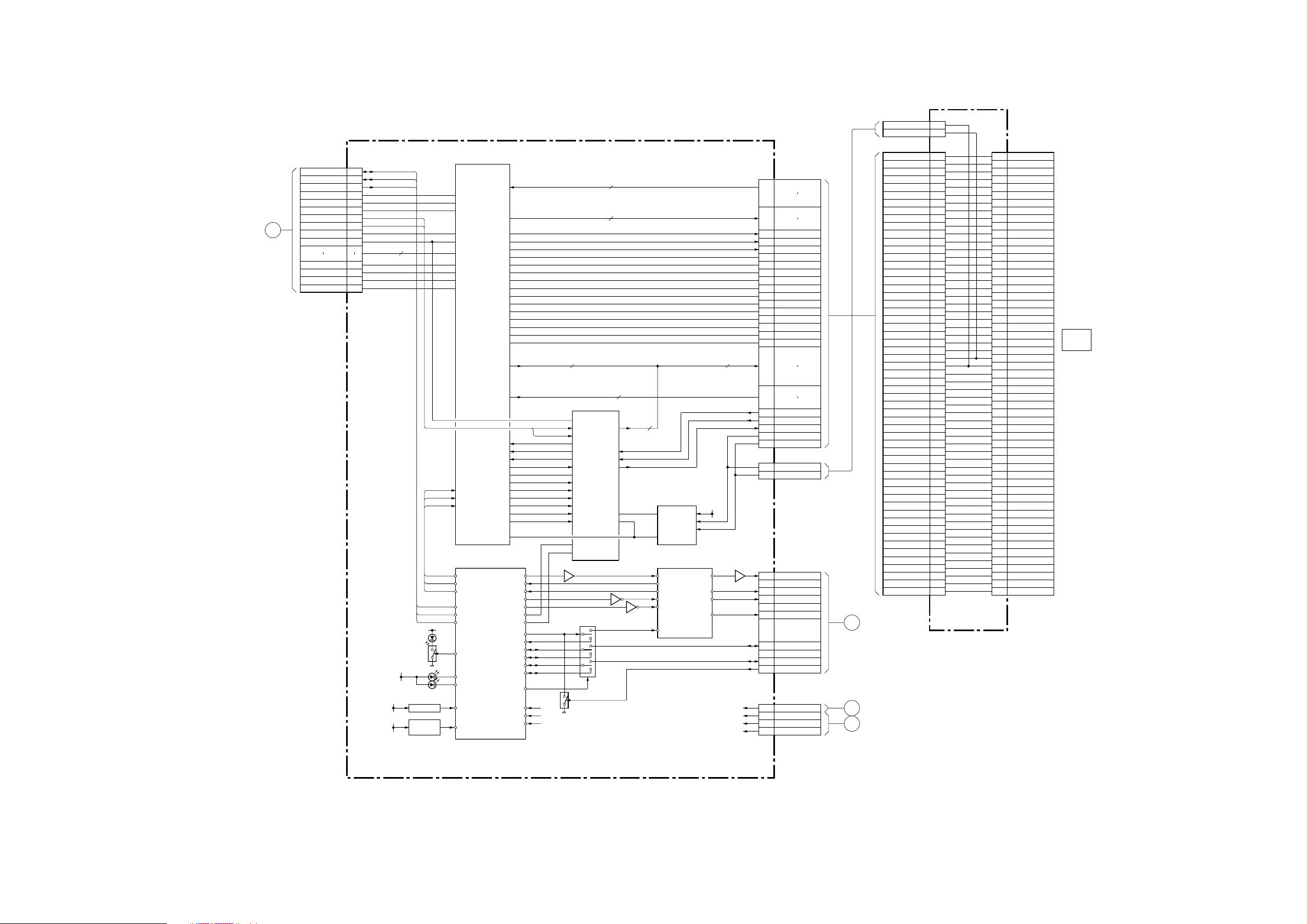
(12) QT AND QU BOARDS
Z
TO
QM BOARD
CN7306
CN7900
FE_SDA
FE_SEL
RESET_FE
RESET_2099
HA1
HA0
CS0
HRW
HIRQ#
HACK
HD0
HD7
FE_SDATA
FE_SCLK
FE_VAL
FE_SYNC
10
12
14
16
18
32
34
36
38
40
1
2
3
4
6
8
FE_SDA
FE_SCL
/RESET_FE
HD0-HD7
8
+3.3V
2.5V
+9V
CLK 5
CLK
VALID
DATA
FE_SCL
FE_SDA
/RESET_FE
D3.3V
D7901
Q7902
Q7906
D7902
D7900
IC7905
1.2V REG
IC7901
DC_DC
CONVERTER
IC7900
POD INTERFACE CONTROL
MCLKI
MIVAL
MCLKO
MISTRT
MOVAL
MOSTRT
WAIT#
IREQ#
IOWR#
IORD#
HRW_SCL
HCS_SDA
VCCSW
A4_CTX
A5_ITX
A6_ETX
A7_QTX
A8_CRX
A9_DRX
VCCSEL
TU7901
TUNER
HD
MDI
95
94
82
93
81
80
68
69
RST
67
61
WE#
59
60
70
VS1#
62
OE#
66
ADOE
A
D
14
13
71
CD#
58
CE1#
33
40
41
42
43
46
47
34
IF_OUT
SAP_IND_I
ST_IND_I
MODE_O
F_MONO_O
POD_CRX
POD_DRX
AGC_IN
AGC_OUT
TU_SDA
TU_SDA0
TU_SCL
TU_SCL0
AGC_SW
7
RESET#
11
HA1
12
HA0_I2CA0
15
HIR0#
16
HACK
HD
27
TOD
28
TOCLK
29
TOVAL
30
TOSTRT
TICLK
4VALID
TIVAL
96DATA
TIDO
MPEG_CLK
MPEG_ENABLE
MPEG_D7/
DEM_SL
DEM_SDA
RESET
MPEG_ERR
FDC_LOCK
FAT_LOCK
D1.2V_DEM
A32V_TU
+9V
+5V
+3.3V
HD0-HD7
MDI0-MDI7
A0-A3,A10-A11
6
D0-D7
IC7904
18
44
CSO#
45
HRW
40
HRW#
41
HCS#
16
CD#
19
CE1#
39
VCCSW
34
A4_CTX
33
A5_ITX
32
A6_ETX
31
A7_QTX
28
A8_CRX
27
A9_DRX
24
FDC_CRX
26
FDC_DRX
Q7901
IC7902
4
5
15
2
14
12
Q7900
8
8
PLD
CD2#
CD1#
CE1_OUT#
BVCC5#
VCCSEL
Q7904
3
1
13
9,10,11
CN7951
VCC
VPP
CD2#
MDO2
CN7103
5,7,9
MDO0
66,68
71,73
MDO7
75
27,30
MDI0
32,34
46,48
MDI7
50,52
MCLKI
33
MIVAL
35
MCLKO
51
MISTRT
55
MOVAL
14
MOSTRT
11
21
WAIT#
RESET
23
IREQ#
47
49 WE#
IOWR#
57
IORD#
59
62 VS1#
63
OE#
64 CE2#
13,15
17,19
22,24
26,29
12
56,58
60,65
10,70
Q7905
+9V
+5V
72,74
76,78
41-45
36-40
8
A4-A9
A
6
14
46
47
IC7903
15
38
POWER I/F SW
27
BVCC5#
26
BVCC3#
NTSC_STEREO_DEMODULATOR
VIF
SAP_IND
ST_IND
MODE
Q7903
F_MONO
RF AGC
AVCC
BVCC
TU7900
LOUT
ROUT
AFCONT
+5V
+3.3V
+2.5V
A0
A11
6,8
D0
D7
CD2#
3
CD1#
77
67
CE1#
VCC
VPP-2
CN7904
1,2 VCC
5 VPP
CN7901
2 TU1VDET OUT2
TU1L6
TU1R4
AFT_M1
9 SDA
8 SCL
10 AGC M
CN7902
2
9V
4
5V
7,8
3.3V
10
2.5V
N
TO
A1U(1/2)BOARD
CN005
A2NU(2/2)BOARD
Y
P
TO
QM BOARD
CN7307
TO
CN8210
MDO1
MDO0
MOSTRT
MOVAL
INPACK#
WAIT#
A4_CTX
RESET
A5_ITX
A6_ETX
MDI7
A7_QTX
MDI6
MDI5
MCLKI
MDI4
MIVAL
VPP-2
VCC
MDI3
IREQ#
MDI2
WE#
MDI1
MCLKO
MDI0
MISTRT
A8_CRX
IOWR#
A9_DRX
IORD#
A11
VS1#
OE#
CE2#
A10
MDO7
CE1#
MDO6
MDO5
MDO4
MDO3
CD1#
1
5
CN7953
5
6
D2
7
8
D1
9
10
D0
11
13
A0
14
15
A1
17
A2
18
19
A3
21
22
23
24
26
27
29
30
32
33
34
35
36
41
46
47
48
49
50
51
52
55
56
57
58
59
60
62
63
64
65
66
67
68
70
D7
71
72
D6
73
74
D5
75
76
D4
77
78
D3
QU
(RELAY BOARD)
B333
B32
A32
B31
A31
B30
A30
B29
A29
B28
A28
A27
B26
A26
B25
A25
B24
A24
A23
B22
A22
B21
B20
A20
B19
A19
B18
A17
B16
A16
B15
A15
B14
A14
B13
B12
A12
B11
A11
B10
A10
B9
A9
B8
A8
B7
A7
B6
A6
B5
A5
B4
A4
B3
A3
B2
A2
B-SS12324<UC.>-QU
CN7952
CD2#
MDO2
MDO1
MDO0
MOSTRT
MOVAL
INPACK#
WAIT#
A4_CTX
RESET
A5_ITX
A6_ETX
MDI7
A7_QTX
MDI6
MDI5
MCLKI
MDI4
MIVAL
VPP-2
MDI3
IREQ#
MDI2
MDI1
MCLKO
MDI0
MISTRT
A8_CRX
IOWR#
A9_DRX
IORD#
VS1#
CE2#
MDO7
CE1#
MDO6
MDO5
MDO4
MDO3
CD1#
D2
D1
D0
A0
A1
A2
A3
VCC
WE#
A11
OE#
A10
D7
D6
D5
D4
D3
CABLE
CARD
(TUNER,POD INTERFACE CONTROL)
QT
KDE-37XS955/42XS955 (UC) 3-12
 Loading...