

Sony ILX522K Datasheet

2048 × 2pixel CCD Linear Sensor (Color)
For the availability of this product, please contact the sales office.
Descriptions
The ILX522K is a reduction type CCD linear
sensor designed for color image scanner use. This
sensor reads B4 size documents at a density of 200
DPI. (Dot Per Inch), and has 2lines analog
memories to adjust the position of green line and
red/blue line. A built-in timing generator and clockdrivers ensure direct drive at 5V logic.
ILX522K
22 pin DIP (Cer-DIP)
Features
• Number of effective pixels: 2048 × 2pixels
• Pixel size
Red/Blue pixel: 14µm × 12µm (14µm pitch)
Green pixel: 14µm × 14µm (14µm pitch)
• Built-in timing generator, clock-drivers
• Ultra-low lag
• Good linearity
• High sensitivity
• Input Clock Pulse: CMOS 5V drive
Absolute Maximum Ratings
• Supply voltage VDD1 11 V
VDD2 6V
Pin Configuration (Top View)
φRS
VDD1
VOUT-R/B
1
2
G1
G2
R1
B1
3
NC
22
GND
21
V
DD2
20
Block Diagram
φROG
GND
9
15
Driver
Clock driver
φV1
12
Driver
Analog memory
CCD analog shift register
φV2
11
Driver
D46
D33
B1024
R1024
Readout gate
Analog memory
B1
R1
D32
D46
D33
G2048
G2047
Readout gate
G2
CCD analog shift register
G1
D32
Clock driver
14
GND
DD2
13
V
10
GND
8
DD1
V
16
φCLK
18
GND
VOUT-G
VDD1
NC
NC
DD1
V
φROG
GND
4
5
6
7
8
9
10
11
G2047
G2048
R1024
B1024
VGG
19
D13
GND
18
NC
17
φCLK
16
GND
15
GND
14
DD2
V
13
φV1φV2
12
Output
amplifier
3
OUT-R/B
V
Driver
1
φRS
Output
amplifier
4
OUT-G
V
D13
19
GG
V
Sony reserves the right to change products and specifications without prior notice. This information does not convey any license by
any implication or otherwise under any patents or other right. Application circuits shown, if any, are typical examples illustrating the
operation of the devices. Sony cannot assume responsibility for any problems arising out of the use of these circuits.
– 1 –
5
21
20
2
E95436-PP
DD1
V
GND
DD2
V
DD1
V
Pin Description
ILX522K
Pin No.
1
2
3
4
5
6
7
8
9
10
11
12
13
14
15
16
Symbol
φRS
VDD1
VOUT-R/B
VOUT-G
VDD1
NC
NC
VDD1
φROG
GND
φV2
φV1
VDD2
GND
GND
φCLK
Description
Clock pulse input
9V power supply
R/B signal out
G signal out
9V power supply
NC
NC
9V power supply
Clock pulse input
GND
Clock pulse input
Clock pulse input
5V power supply
GND
GND
Clock pulse input
17
18
19
20
21
22
NC
GND
VGG
VDD2
GND
NC
NC
GND
Output gate bias
5V power supply
GND
NC
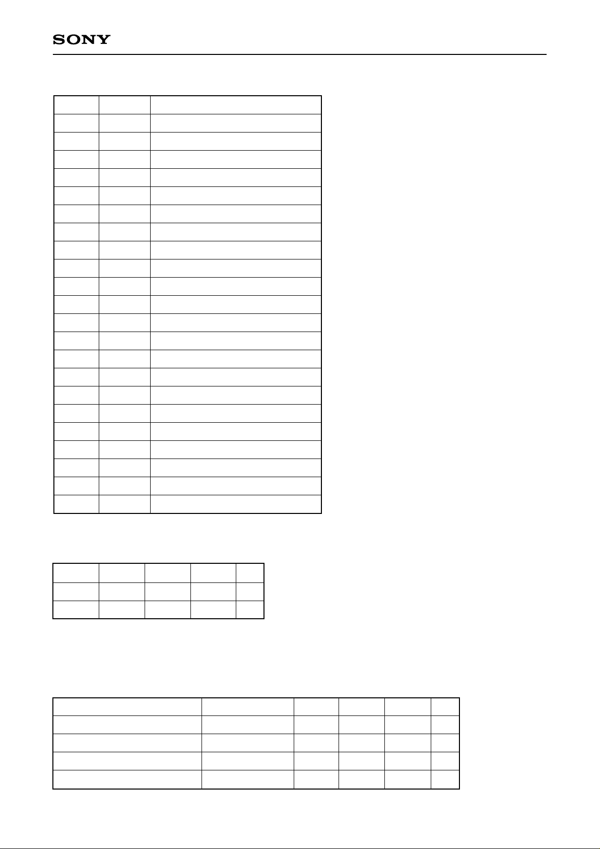
Recommended Supply Voltage
Item
VDD1
VDD2
Min.
8.5
4.75
Typ.
9.0
5.0
Max.
9.5
5.25
Unit
V
V
Note) Rules for raising and lowering power supply voltage.
To raise power supply voltage, first raise VDD1 (9V) and then VDD2 (5V).
To lower voltage, first lower VDD2 (5V) and then VDD1 (9V).
Clock Characteristics
Item Symbol Min. Typ. Max. Unit
Input capacity of φRS, φCLK
Input capacity of φV1, φV2
Input capacity of φROG
Input clock frequency
CφRS, CφCLK
CφV1, CφV2
CφROG
fφRS, fφCLK
– 2 –
—
—
—
—
10
10
10
—
—
—
—
3.5
pF
pF
pF
MHz

Electrical Characteristics (Note 1)
A
(Ta = 25°C, VDD1 = 9V, VDD2 = 5V fφRS = 3.5MHz Light source = 3200K, IR cut filter CM-500S (t = 1.0mm))
Item Symbol Min. Typ. Max. Unit Remarks
ILX522K
Red
Sensitivity
Sensitivity nonuniformity
Saturation output voltage
Dark voltage average
Dark signal nonuniformity
Image lag
9V supply current
5V supply current
Total transfer efficiency
Output impedance
Offset level
Note:
1) In accordance with the given electrooptical characteristics, the black level is defined as the average of D3,
D4, to D10.
2) For the sensitivity test light is applied with a uniform intensity of illumination.
3) PRNU is defined as indicated below in each color. Ray incidence conditions are the same as for Note 2.
Green
Blue
Green
Red/Blue
Green
Red/Blue
RR
RG
RB
PRNU
VSAT
VDRK-G
VDRK-R/B
DSNU-G
DSNU-R/B
IL
IVDD1
IVDD2
TTE
ZO
VOS
5.2
6.5
2.8
—
1.0
—
—
—
—
—
—
—
92.0
—
—
8.0
10.0
4.3
5.0
1.5
0.3
1.5
0.6
2.0
0.02
20
16.0
98.0
150
5.4
10.8
13.5
5.8
15.0
—
1.5
9.0
3.0
12.0
—
40
32.0
—
—
—
V/(lx · s)
%
V
mV
%
mA
mA
%
Ω
V
Note 2
Note 3
Note 4
Note 5
Note 6
—
—
—
—
Note 7
PRNU = × 100 [%]
The maximum output of each color is set to VMAX, the minimum output to VMIN, and the average output to
VAVE.
4) Use below the minimum value of the saturation output voltage.
5) Optical signal accumulated time τint stands at 5ms.
6) VOUT-G = 500mV (Typ.)
7) VOS is defined as indicated below.
(VMAX – VMIN)/2
VAVE
∗
VOUT
A
OS
V
GND
∗
VOUT indicates VOUT-G and VOUT-R/B.
– 3 –

ILX522K
2088 2094
D46
D40
D39
D33 D34
G2048
G2047
G2046
G1 G2
D32
D46
D40
D39
D33 D34
B1024
R1024
B1023
B1
R1
D32
1 Line Output (2094 pixels)
5V
0V
φROG
Clock Timing Chart
5V
φV1
0V
5V
φV2
0V
5V
123
0 0
φCLK
0V
5V
φRS
0V
OUT-G
V
D1 D2 D3 D12 D13 D14 D30 D31
Optical Black (18 pixels)
Dummy Signal (32 pixels)
D1 D2 D3 D12 D13 D14 D30 D31
VOUT-R/B
Note) φCLK, φRS pulses must have more than 2094 cycles.
– 4 –
 Loading...