

Page 1
ICF-S79/S79L/S79V
e
SERVICE MANUAL
Ver 1.2 2002.02
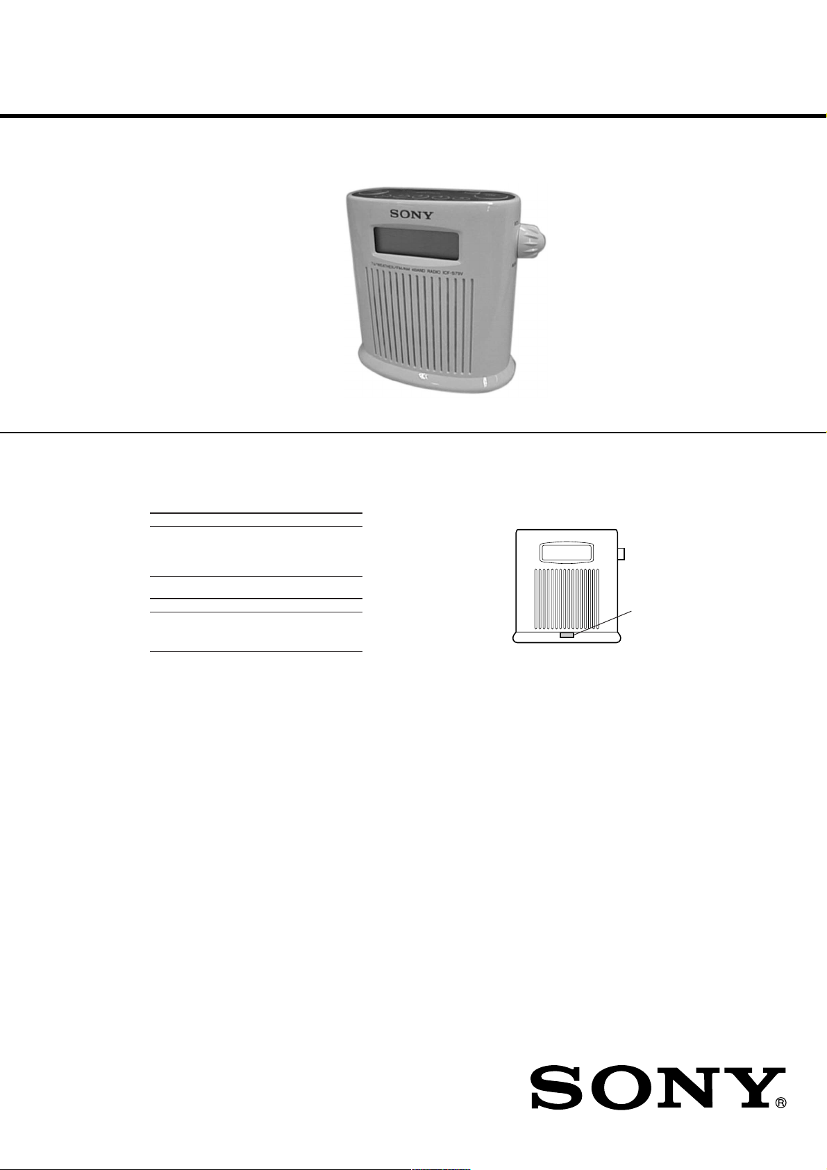
Photo: ICF-S79V (Original Type)
SPECIFICATIONS
Frequency range:
Model for North and South America
Band ICF-S79V Channel step
FM 87.5 – 108 MHz 0.1 MHz
AM 530 – 1,710 kHz 10 kHz
TV 2 – 13 ch —
WEATHER 1 – 5 ch —
Model for other countries
Band
ICF-S79 ICF-S79L
FM
87.5 – 108 MHz 87.5 – 108 MHz 0.05 MHz*
AM(MW) 531 – 1,602 kHz 531 – 1,602 kHz 9 kHz
LW
— 153 – 279 kHz 9 kHz
* The frequency display is raised or lowered by steps of
0.1 MHz. For example, both 88.00 MHz and 88.05 MHz
will be displayed as “88.0 MHz.”
Time display:
Model for North and South America: 12-hour
system
Model for other countries: 24-hour system
Speaker:
Power output:
Power requirements:
Dimensions: Approx. 143.5 x 139 x 67 mm
Mass: Approx. 523 g (1lb 2oz) incl. batteries
Supplied accessories: Suction cup (1), Strap (1)*
Design and specifications are subject to change
without notice.
1
7.7 cm (3
220 mW (at 10% harmonic distortion)
4.5 V DC, three size C (R14) batteries
(w/h/d) (Approx. 5
inches) incl. projecting parts and controls
*North and South American model only
/8 inches), 8 ohms
3
/4 x 5 1/2 x 2 3/
Channel Step
4
US Model
ICF-S79V
AEP Model
ICF-S79/S79L
UK Model
ICF-S79L
MODEL IDENTIFICATION
There are two types of ICF-S79V.
Please look at the mark of set shown below.
no mark: Original Typ
Liv : Liv Type
Notes on chip component replacement
• Never reuse a disconnected chip component.
• Notice that the minus side of a tantalum capacitor may be dam-
aged by heat.
ICF-S79
FM/AM SYNTHESIZED RADIO
ICF-S79L
TV/WEATHER/FM/AM SYNTHESIZED RADIO
9-925-738-12 Sony Corporation
2002B0500-1 Personal Audio Company
C 2002.02 Published by Sony Engineering Corporation
FM/MW/LW SYNTHESIZED RADIO
ICF-S79V
Page 2
This section is extracted from
instruction manual.
SECTION 1
GENERAL
– 2 –
Page 3
– 3 –
Page 4
SECTION 2
d
DISASSEMBLY
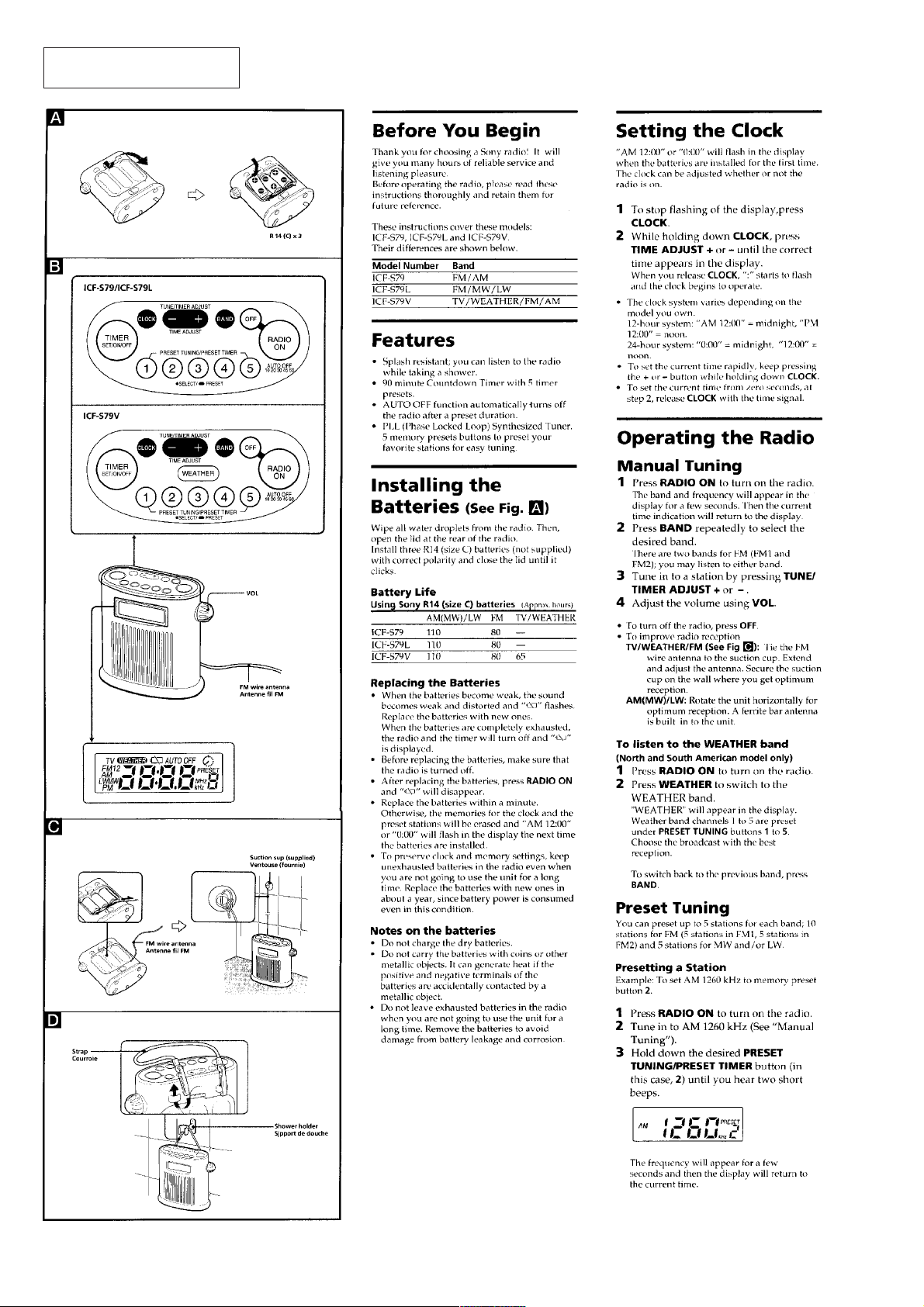
Note: Follow the disassembly procedure in the numerical order given.
REAR CABINET
5
BATT lead (red)
3
two claws
5
antenna lead
4
rear cabinet
2
six screws
(BTP 3 × 25)
1
battery case li
5
BATT lead (white)
– 4 –
Page 5
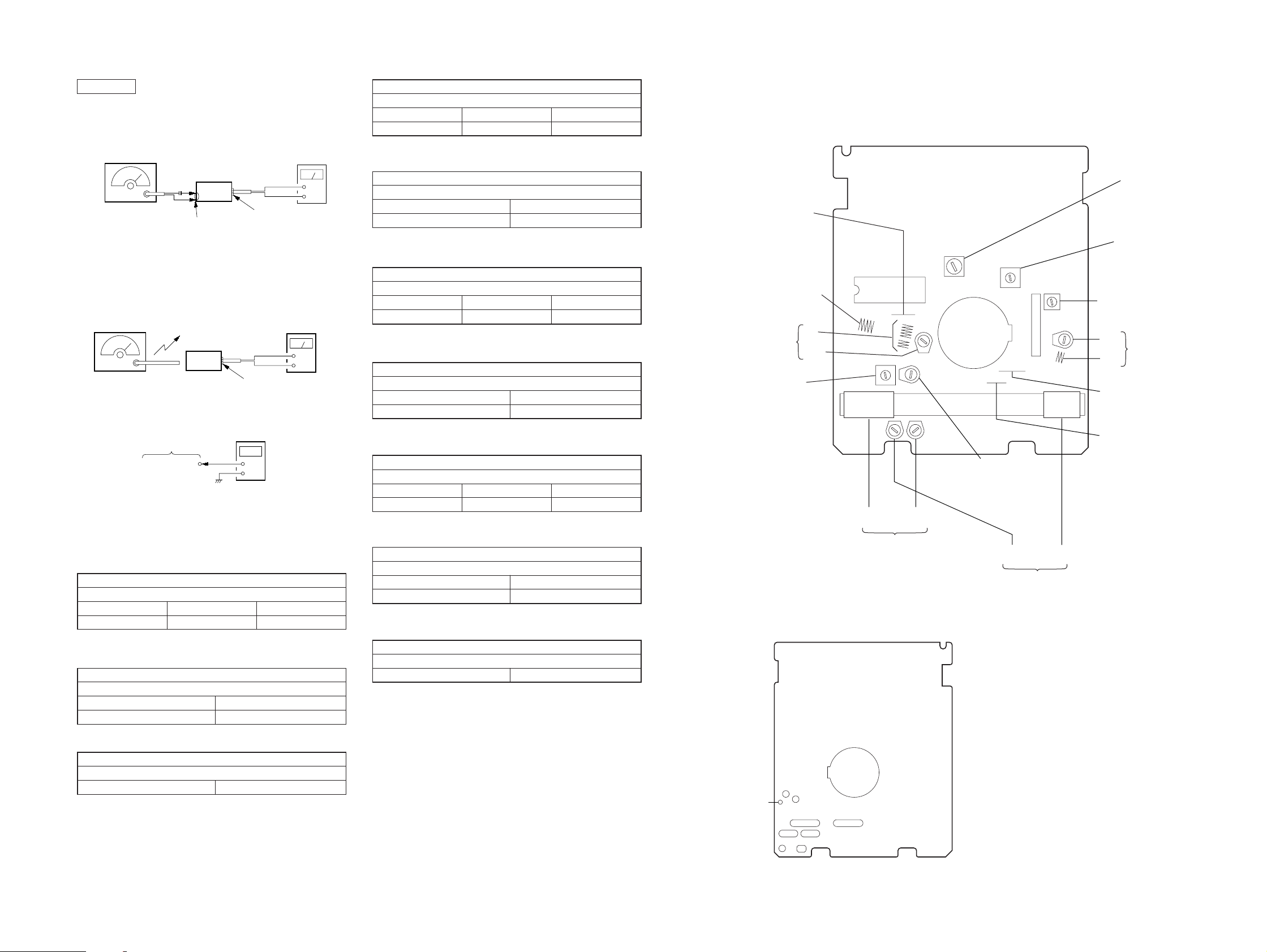
SECTION 3
FM antenna
ground
(JW17)
L8
FM FREQUENCY
COVERAGE
L9
AM (MW)
FREQUENCY
COVERAGE
L5 CT3
AM (MW)
TRACKING
TV TRACKING
(ICF-S79V only)
T1
TV IF
(ICF-S79V only)
L2
TV FREQUENCY
COVERAGE
(ICF-S79V only)
CT5
LW FREQUENCY
COVERAGE
(ICF-S79L only)
TV antenna
ground
(JW20)
FM/TV
antenna input
(JW18)
CT1
L1
T2
AM IF
FM
TRACKING
L6
CT4
CT2 L5
LW TRA CKING
(ICF-S79L only)
MW LWL5
IC1
IC2
TP
(VT)
r
ELECTRICAL ADJUSTMENTS
0dB=1 µV
[FM/TV Section]
Setting:
BAND switch: FM1 or TV
FM RF SSG
0.01
µ
F
±
22.5 kHz frequency
deviation by 400 Hz
signal
Output level: as low as possible
FM lead wire antenna terminal
[AM (LW/MW) Section]
Setting:
BAND switch: AM (MW) or LW
Put the lead-wire
AM RF SSG
30% amplitude
modulation by
400 Hz signal
Output level: as low as possible
antenna close to
the set.
set
set
speaker terminal
level meter
+
–
speaker terminal
level meter
+
–
FM FREQUENCY COVERAGE ADJUSTMENT
Adjust for a reading on digital voltmeter.
L8 87.5 MHz (TV 2 ch)
Confirm 108.0 MHz
Note: Not use the FM RF signal generator in this adjustment.
2.3 ± 0.1 V (1.0 ± 0.1 V)
8.5 ± 0.5 V (12.5 ± 0.5 V)
( ): ICF-S79V
FM TRACKING ADJUSTMENT
Adjust for a maximum reading on level meter.
L6 87.5 MHz (TV 2 ch (59.75 MHz))
CT4 108.0 MHz
( ): ICF-S79V
ICF-S79L only
LW FREQUENCY COVERAGE ADJUSTMENT
Adjust for a reading on digital voltmeter.
CT5 153 kHz 2.3 ± 0.1 V
Confirm 279 kHz 8.5 ± 0.5 V
Note: Not use the AM RF signal generator in this adjustment.
ICF-S79L only
LW TRACKING ADJUSTMENT
Adjust for a maximum reading on level meter.
L5 (LW side) 162 kHz
CT2 243 kHz
Adjustment and Connection Location:
[MAIN BOARD] (Component Side)
MAIN board
TP
(VT)
digital voltmete
+
–
Repeat the procedures in each adjustment several times, and the
frequency coverage and tracking adjustments should be finally done
by the trimmer capacitors.
ICF-S79V only
TV FREQUENCY COVERAGE ADJUSTMENT
Adjust for a reading on digital voltmeter.
L2 WEATHER 2 ch 1.0 ± 0.1 V
Confirm TV 13 ch 10 ± 0.5 V
Note: Not use the FM RF signal generator in this adjustment.
ICF-S79V only
TV TRACKING ADJUSTMENT
Adjust for a maximum reading on level meter.
L1 WEATHER 2 ch (162.40 MHz)
CT1 TV 13 ch (215.75 MHz)
ICF-S79V only
Adjust for a maximum reading on level meter.
TV IF ADJUSTMENT
T1 10.7 MHz
AM (MW) FREQUENCY COVERAGE ADJUSTMENT
Adjust for a reading on digital voltmeter.
L9 531 kHz (530 kHz) 2.8 ± 0.1 V
Confirm 1,602 kHz (1,710 kHz) 9.5 ± 0.5 V
Note: Not use the AM RF signal generator in this adjustment.
AM (MW) TRACKING ADJUSTMENT
Adjust for a maximum reading on level meter.
L5 <MW side> 621 kHz (590 kHz)
CT3 1,395 kHz (1,490 kHz)
AM IF ADJUSTMENT
Adjust for a maximum reading on level meter.
T2 455 kHz
( ): ICF-S79V
< >: ICF-S79L
( ): ICF-S79V
[MAIN BOARD] (Conductor Side)
– 5 –
– 6 –
Page 6
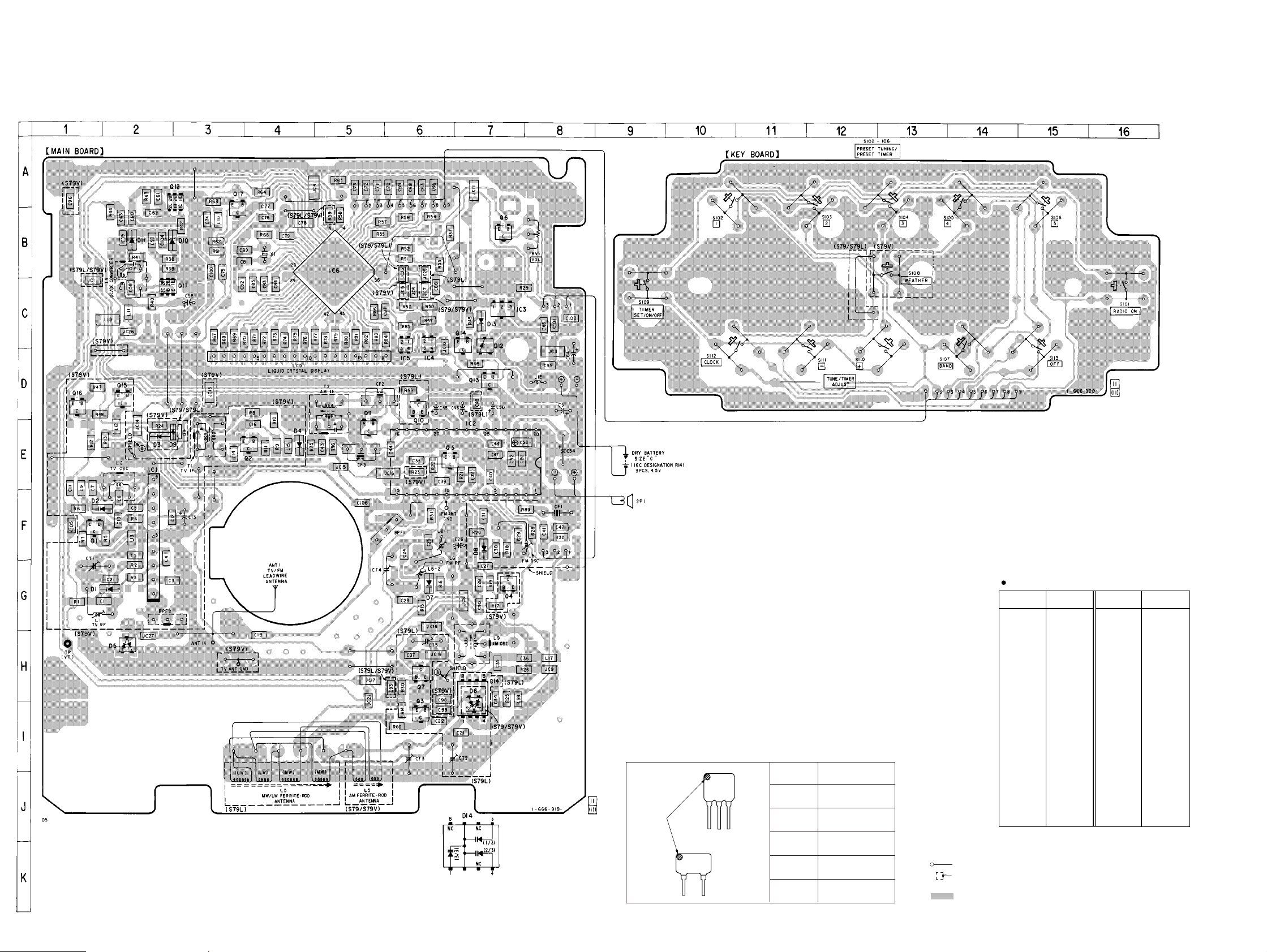
ICF-S79/S79L/S79V
4-1. PRINTED WIRING BOARDS
SECTION 4
DIAGRAMS
HOW TO CHANGE THE CERAMIC FILTERS
This model is used two ceramic filters of CF1, CF3.
Y ou must use same type of color marked cer amic filters in order to
meet same specifications.
Therefore, the ceramic filter must change two pieces together since
it's supply two pieces in one package as a spare parts.
Mark Center frequency
CF3
mark
CF1
red 10.70 MHz
blue 10.67 MHz
orange 10.73 MHz
black 10.64 MHz
white 10.76 MHz
Semiconductor Location
Ref. No. Location Ref. No. Location
D1 G-1 Q1 F-1
D2 F-1 Q2 E-4
D3 E-2 Q3 I-6
D4 E-4 Q4 G-7
D5 H-2 Q5 E-6
D6 H-7 Q6 B-7
D7 G-6 Q7 H-6
D8 F-7 Q9 E-5
D9 E-2 Q10 D-6
D10 B-2 Q11 C-2
D11 B-2 Q12 A-2
D12 C-7 Q13 D-7
D13 C-7 Q14 C-7
D14 H-7 Q15 D-2
IC1 F-2 Q17 A-3
IC2 E-7
IC3 C-7
IC4 C-6
IC5 C-6
IC6 B-5
Note on Printed Wiring Board:
• : parts extracted from the component side.
• : indicates side identified with part number.
¢
•
• : Pattern from the side which enables seeing.
: internal component.
Q16 D-1
– 7 –
– 8 –
Page 7
4-2. SCHEMATIC DIAGRAM (ICF-S79/S79L) • See page 11 for Waveforms and IC Block Diagrams.
ICF-S79/S79L/S79V
Note on Schematic Diagram:
• All capacitors are in µF unless otherwise noted. pF: µµF
50 WV or less are not indicated except for electrolytics
and tantalums.
• All resistors are in Ω and 1/
specified.
• ¢ : internal component.
• : panel designation.
•
B+: B+ Line.
• : adjustment for repair.
• Power voltage is dc 4.5 V and fed with regulated dc power
supply from battery terminal.
• Voltages and waveforms are dc with respect to ground
under no-signal (detuned) conditions.
no mark : FM (TV 2 – 6 ch)
( ) : AM (MW)
[]: LW
W or less unless otherwise
4
• Voltages are taken with a V OM (Input impedance 10 MΩ).
V oltage variations may be noted due to normal production
tolerances.
• Waveforms are taken with a oscilloscope.
V oltage variations may be noted due to normal production
tolerances.
• Circled numbers refer to waveforms.
• Signal path.
: FM
: AM (MW/LW)
– 9 –
– 10 –
Page 8
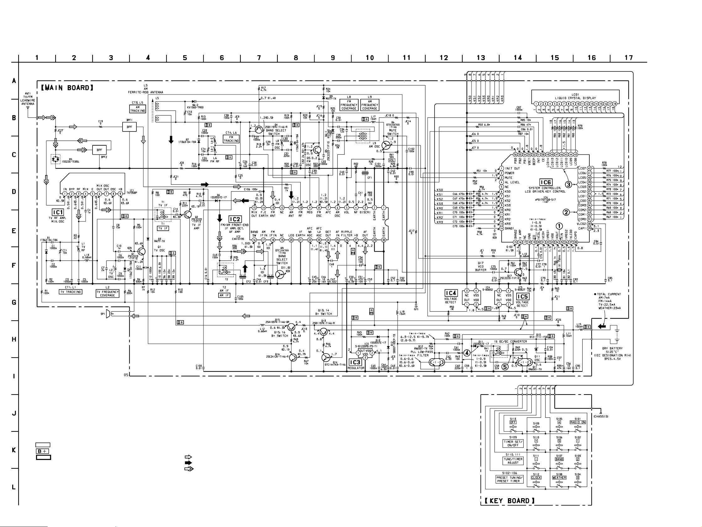
ICF-S79/S79L/S79V
4-3. SCHEMATIC DIAGRAM (ICF-S79V) • See page 11 for Waveforms and IC Block Diagrams.
Note on Schematic Diagram:
• All capacitors are in µF unless otherwise noted. pF: µµF 50
WV or less are not indicated except for electrolytics and
tantalums.
• All resistors are in Ω and 1/
specified.
• ¢ : internal component.
• : panel designation.
• : B+ Line.
• : adjustment f or repair.
• Power voltage is dc 4.5 V and fed with regulated dc power
supply from battery terminal.
• Voltages and wavef orms are dc with respect to ground under no-signal (detuned) conditions.
no mark : FM (TV 2 – 6 ch)
( ) : AM
<< >> : TV (7 – 13 ch)
W or less unless otherwise
4
• Voltages are taken with a VOM (Input impedance 10 MΩ).
V oltage variations may be noted due to normal production
tolerances.
• Waveforms are taken with a oscilloscope.
V oltage variations may be noted due to normal production
tolerances.
• Circled numbers refer to waveforms.
• Signal path.
: FM
: AM
: TV
– 11 –
– 12 –
Page 9

• Wavef orms
• IC Block Diagrams
1 IC6 @∞ (XIN)
13.3 µs
2 IC6 #¡ – #¢ (COM0 – COM3)
32 ms
3 IC6 #∞ – $• (LCD0 – LCD13)
2 Vp-p
3 Vp-p
3 Vp-p
IC1 TA7358P (ICF-S79V only)
REGULATOR
BIAS
RF
MIX OSC
5 6 7 8 9
4
MIX
RF OUT
GND
MIX OUT
OSC OUT
OSC
1
RF IN
AMP
2 3
BYPASS
IC2 CXA1019S
GND
GND
AF OUT
VCC
RIPPLE
FILTER
AF IN
DET OUT
AFC AGC
AFC AGC
FM FE
FM OSC
REG OUT
IF GND
TUNING
METER
FM RF
23 22 21 202425 19 18 17 1629 28 27 2630
AM IF DET AGC
AF POWER AMP AM FE FM IF
FM
DISCRIMINATOR
2 3
1
GND
GND
5 6 7 8 9 10 1514131211
4
NF
FM DISCRI
VOL
AFC
AM OSC
VCC
METER
AM RF IN
N.C
N.C
FM IF IN
FE GND
FM RF IN
AM IF IN
FM/AM BAND
SELECT
IF OUT
FM/AM
32 ms
4 D11 ANODE
440 ns
5 Q11-1 COLLECTOR
360 ns
30 Vp-p
6 Vp-p
– 13 –
Page 10

4-4. IC PIN FUNCTION DESCRIPTION
MAIN BOARD IC6 µPD17071GB-517-1A7
(SYSTEM CONTROLLER, LIQUID CRYSTAL DISPLAY CONTROLLER, KEY CONTROL)
Pin No. Pin Name I/O Function
1 INIT OUT O
2 POWER O
3 MUTE O
4 AL LEVEL O
5NCO
6 to 9 KS0 to KS3 O
10 to 13 KR0 to KR3 I
14 BAND1 O
15 BAND2 O
16 V AMP —
17 NC O
18 GND —
19 EO O
20 VCOL I
21 VCOH I
22 VREG1 —
23 VDD —
24 XOUT O
25 XIN I
26 VREG2 —
27 VLCD0 —
28 CAP0 —
29 CAP1 —
30 VLCD2 —
31 to 34 COM0 to COM3 O
35 to 48 LCD0 to LCD13 O
49 LCD14 O
50 CE I
51 INT I
52 BEEP O
53 VDET I
54 PB1 I
55 PB2 I
56 PB3 I
Initialize signal output for the destination select
Radio power on/off control signal output “H”: power on
Mute on/off control signal output “L”: mute on
Beep sound level variable output terminal Not used (open)
Not used (open)
Key strobe signal output terminal
Key return signal input terminal
Band select signal output terminal *1
Band select signal output terminal *1
Used for ICF-S79L/S79V only (ICF-S79: not used (open))
Power supply terminal for buffer amplifier
Not used (open)
Ground terminal
PLL error signal output terminal
AM (MW) or LW VCO input terminal
FM, TV or WEATHER VCO input terminal
Power supply terminal (connected to the coupling capacitor)
Power supply terminal (+2.2 V)
System clock output terminal (75 kHz)
System clock input terminal (75 kHz)
Power supply terminal (connected to the coupling capacitor)
Terminal for doubler circuit capacitor connection to develop liquid crystal display drive
voltage
Common drive signal output to the liquid crystal display (LCD1)
Segment drive signal output to the liquid crystal display (LCD1)
Segment drive signal output terminal Not used (open)
Power failure detection signal input from the IC5 Normally: “H”
Not used (fixed at “L”)
Beep sound drive signal output terminal
Power failure detection signal input from the IC4 Normally: “H”
Initialize signal input for the destination select Fixed at “L”
Initialize signal input for the destination select
ICF-S79/S79L: initialize mode at “H”, ICF-S79V: fixed at “L”
Initialize signal input for the destination select
ICF-S79L: initialize mode at “H”, ICF-S79/S79V: fixed at “L”
*1 Band select signal
BAND1 (pin !¢)
BAND2 (pin !∞)
FM (TV L)
“L” “L” “H” “H”
“L” “H” “L” “H”
TV H/
WEATHER
AM (MW) LW
– 14 –
Page 11

SECTION 5
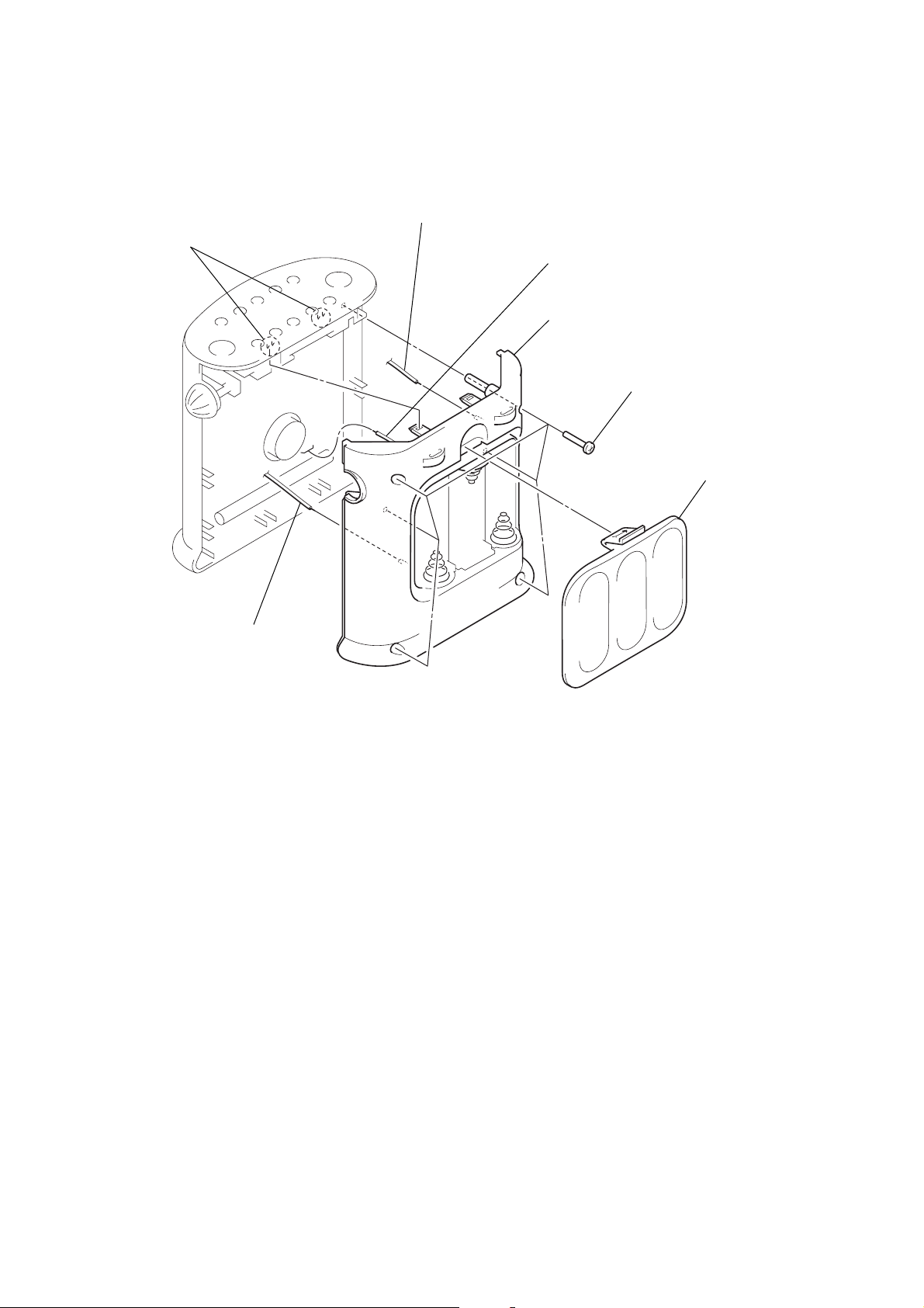
EXPLODED VIEW
Ver 1.2
NOTE:
• -XX and -X mean standardized parts, so they
may have some difference from the original one.
• Color Indication of Appearance Parts
Example:
KNOB, BALANCE (WHITE) . . . (RED)
↑↑
Parts Color Cabinet's Color
4
2
not supplied
3
1
• Items marked “*” are not stocked since they
are seldom required for routine service. Some
delay should be anticipated when ordering these
items.
• The mechanical parts with no reference number in the exploded views are not supplied.
• Accessories and packing materials are gi ven in
the last of the electrical parts list.
7
6
14
LCD1
not supplied
• Please refer to model identification (page
1) for system of original type and Liv
type.
9
8
not supplied
11
10
12
13
15
17
18
Ref. No. Part No. Description Remark
1 X-3374-190-1 CABINET (FRONT) ASSY (S79V: Original type)
1 X-3374-190-2 CABINET (FRONT) ASSY (S79L)
1 X-3374-190-3 CABINET (FRONT) ASSY (S79)
1 X-3374-190-6 CABINET (FRONT) ASSY (S79V: Liv type)
2 3-016-880-01 PLATE (BUTTON), SHEET (S79V: Original type)
2 3-016-880-11 PLATE (BUTTON), SHEET (S79/S79L)
2 3-016-880-31 PLATE (BUTTON), SHEET (S79V: Liv type)
* 3 3-016-863-01 CHASSIS
* 4 A-3679-918-A MAIN BOARD, COMPLETE (S79)
* 4 A-3679-919-A MAIN BOARD, COMPLETE (S79V)
* 4 A-3679-921-A MAIN BOARD, COMPLETE (S79L)
6 3-016-875-01 SHEET (BATTERY) (A)
7 3-016-869-01 TERMINAL (+), BATTERY
8 3-016-861-01 CABINET (REAR)
(S79/S79L/S79V: Original type)
8 3-016-861-31 CABINET (REAR) (S79V: Liv type)
16
SP1
Ref. No. Part No. Description Remark
9 3-016-871-01 TERMINAL (+.–) (A), BATTERY
10 3-016-872-01 TERMINAL (+.–) (B), BATTERY
11 3-016-870-01 TERMINAL (–), BATTERY
12 7-685-152-19 SCREW +BTP 3X25 TYPE2 N-S
13 3-016-876-01 SHEET (BATTERY) (B)
14 3-368-852-01 FOOT
15 3-016-862-01 LID, BATTERY CASE
(S79/S79L/S79V: Original type)
15 3-016-862-21 LID, BATTERY CASE (S79V: Liv type)
16 3-016-867-01 SPRING, SP
17 3-016-873-01 SPRING, RING
18 3-016-864-01 KNOB (VOL) (S79/S79L/S79V: Original type)
18 3-016-864-21 KNOB (VOL) (S79V: Liv type)
SP1 1-504-918-11 SPEAKER (7.7CM)
LCD1 1-801-854-11 DISPLAY PANEL, LIQUID CRYSTAL
– 15 –
Page 12

KEY
MAIN
SECTION 6
ELECTRICAL PARTS LIST
NOTE:
• Due to standardization, replacements in the
parts list may be different from the parts specified in the diagrams or the components used on
the set.
• -XX and -X mean standardized parts, so they
may have some difference from the original one.
• RESISTORS
All resistors are in ohms.
METAL: Metal-film resistor .
METAL OXIDE: Metal oxide-film resistor.
F: nonflammable
Ref. No. Part No. Description Remark
KEY BOARD (INCLUDED MAIN BOARD)
**********
< SWITCH >
S101 1-554-303-21 SWITCH, TACTILE (RADIO ON)
S102 1-554-303-21 SWITCH, TACTILE
(PRESET TUNIG/PRESET TIMER 1)
S103 1-554-303-21 SWITCH, TACTILE
(PRESET TUNIG/PRESET TIMER 2)
S104 1-554-303-21 SWITCH, TACTILE
(PRESET TUNIG/PRESET TIMER 3)
S105 1-554-303-21 SWITCH, TACTILE
(PRESET TUNIG/PRESET TIMER 4)
S106 1-554-303-21 SWITCH, TACTILE
(PRESET TUNIG/PRESET TIMER 5)
S107 1-554-303-21 SWITCH, TACTILE (BAND)
S108 1-554-303-21 SWITCH, TACTILE (WEATHER) (S79V)
S109 1-554-303-21 SWITCH, TACTILE (TIMER SET/ON/OFF)
S110 1-554-303-21 SWITCH, TACTILE (TUNE/TIMER ADJUST +)
S111 1-554-303-21 SWITCH, TACTILE (TUNE/TIMER ADJUST –)
S112 1-554-303-21 SWITCH, TACTILE (CLOCK)
S113 1-554-303-21 SWITCH, TACTILE (OFF)
************************************************************
• Items marked “*” are not stocked since they
are seldom required for routine service.
Some delay should be anticipated when ordering these items.
• SEMICONDUCTORS
In each case, u: µ, for example:
uA. . : µA. . uPA. . : µPA. .
uPB. . : µPB. . uPC. . : µPC. .
uPD. . : µPD. .
• CAPACITORS
uF: µF
• COILS
uH: µH
When indicating parts by reference
number, please include the board.
Ref. No. Part No. Description Remark
C4 1-163-217-11 CERAMIC CHIP 1PF 0.25PF50V
(S79V)
C5 1-163-141-00 CERAMIC CHIP 0.001uF 5% 50V
(S79V)
C6 1-163-141-00 CERAMIC CHIP 0.001uF 5% 50V
(S79V)
C7 1-163-085-00 CERAMIC CHIP 2PF 0.25PF50V
(S79V)
C8 1-163-231-11 CERAMIC CHIP 15PF 5% 50V
(S79V)
C9 1-163-141-00 CERAMIC CHIP 0.001uF 5% 50V
(S79V)
C10 1-163-217-11 CERAMIC CHIP 1PF 0.25PF50V
(S79V)
C11 1-163-009-11 CERAMIC CHIP 0.001uF 10% 50V
(S79V)
C12 1-163-009-11 CERAMIC CHIP 0.001uF 10% 50V
(S79V)
C13 1-124-584-00 ELECT 100uF 20% 10V
(S79V)
C14 1-164-232-11 CERAMIC CHIP 0.01uF 50V
(S79V)
C15 1-164-232-11 CERAMIC CHIP 0.01uF 50V
(S79V)
* A-3662-876-A MAIN BOARD, COMPLETE (S79)
* A-3662-879-A MAIN BOARD, COMPLETE (S79V)
* A-3662-888-A MAIN BOARD, COMPLETE (S79L)
(INCLUDING KEY BOARD)
**********************
* 3-016-863-01 CHASSIS
< BAND PASS FILTER >
BPF1 1-236-711-21 FILTER, BAND PASS (S79/S79L)
BPF1 1-239-813-21 FILTER, BAND PASS (S79V)
BPF2 1-233-521-11 FILTER, BAND PASS (S79V)
< CAPACITOR/CHIP CONDUCTOR >
C1 1-163-141-00 CERAMIC CHIP 0.001uF 5% 50V
C2 1-163-141-00 CERAMIC CHIP 0.001uF 5% 50V
C3 1-163-009-11 CERAMIC CHIP 0.001uF 10% 50V
(S79V)
(S79V)
(S79V)
– 16 –
C16 1-164-232-11 CERAMIC CHIP 0.01uF 50V
(S79V)
C19 1-216-295-00 CONDUCTOR, CHIP (2012)
C21 1-163-118-00 CERAMIC CHIP 110PF 5% 50V
(S79L)
C22 1-163-133-00 CERAMIC CHIP 470PF 5% 50V
(S79L)
C23 1-163-141-00 CERAMIC CHIP 0.001uF 5% 50V
C24 1-163-141-00 CERAMIC CHIP 0.001uF 5% 50V
C25 1-216-295-91 CONDUCTOR, CHIP (2012)
C26 1-104-396-11 ELECT 10uF 20% 16V
C27 1-163-141-00 CERAMIC CHIP 0.001uF 5% 50V
(S79V)
C27 1-216-295-00 CONDUCTOR, CHIP (2012) (S79/S79L)
C28 1-164-232-11 CERAMIC CHIP 0.01uF 50V
C29 1-163-085-00 CERAMIC CHIP 2PF 0.25PF50V
C30 1-163-141-00 CERAMIC CHIP 0.001uF 5% 50V
C31 1-163-125-00 CERAMIC CHIP 220PF 5% 50V
C32 1-163-085-00 CERAMIC CHIP 2PF 0.25PF50V
C33 1-163-009-11 CERAMIC CHIP 0.001uF 10% 50V
Page 13

MAIN
Ref. No. Part No. Description Remark Ref. No. Part No. Description Remark
C34 1-164-232-11 CERAMIC CHIP 0.01uF 50V
C35 1-163-131-00 CERAMIC CHIP 390PF 5% 50V
C36 1-163-229-11 CERAMIC CHIP 12PF 5% 50V
C37 1-163-128-00 CERAMIC CHIP 300PF 5% 50V
(S79L)
C38 1-163-251-11 CERAMIC CHIP 100PF 5% 50V
C39 1-164-232-11 CERAMIC CHIP 0.01uF 50V
C40 1-164-232-11 CERAMIC CHIP 0.01uF 50V
C41 1-164-346-11 CERAMIC CHIP 1uF 16V
C42 1-164-232-11 CERAMIC CHIP 0.01uF 50V
C43 1-163-251-11 CERAMIC CHIP 100PF 5% 50V
C44 1-164-232-11 CERAMIC CHIP 0.01uF 50V
C45 1-126-163-11 ELECT 4.7uF 20% 50V
C46 1-104-396-11 ELECT 10uF 20% 16V
C47 1-163-037-11 CERAMIC CHIP 0.022uF 10% 25V
C93 1-164-232-11 CERAMIC CHIP 0.01uF 50V
(S79L/S79V)
C95 1-163-038-00 CERAMIC CHIP 0.1uF 25V
C96 1-163-229-11 CERAMIC CHIP 12PF 5% 50V
(S79V)
C98 1-163-235-11 CERAMIC CHIP 22PF 5% 50V
(S79V)
C99 1-163-229-11 CERAMIC CHIP 12PF 5% 50V
(S79V)
C100 1-164-232-11 CERAMIC CHIP 0.01uF 50V
C101 1-163-009-11 CERAMIC CHIP 0.001uF 10% 50V
C102 1-163-251-11 CERAMIC CHIP 100PF 5% 50V
C104 1-164-232-11 CERAMIC CHIP 0.01uF 50V
C105 1-163-251-11 CERAMIC CHIP 100PF 5% 50V
C106 1-163-251-11 CERAMIC CHIP 100PF 5% 50V
C48 1-164-346-11 CERAMIC CHIP 1uF 16V
C49 1-163-809-11 CERAMIC CHIP 0.047uF 10% 25V
C50 1-123-618-11 ELECT 22uF 20% 6.3V
C51 1-126-925-11 ELECT 470uF 20% 10V
C52 1-164-004-11 CERAMIC CHIP 0.1uF 10% 25V
C53 1-135-091-00 TANTALUM CHIP 1uF 20% 16V
C54 1-126-925-11 ELECT 470uF 20% 10V
C56 1-104-396-11 ELECT 10uF 20% 16V
C57 1-164-346-11 CERAMIC CHIP 1uF 16V
C58 1-163-235-11 CERAMIC CHIP 22PF 5% 50V
C59 1-164-346-11 CERAMIC CHIP 1uF 16V
C60 1-163-125-00 CERAMIC CHIP 220PF 5% 50V
C61 1-163-009-11 CERAMIC CHIP 0.001uF 10% 50V
C62 1-110-501-11 CERAMIC CHIP 0.33uF 10% 16V
C63 1-164-232-11 CERAMIC CHIP 0.01uF 50V
C64 1-126-916-11 ELECT 1000uF 20% 6.3V
C65 1-163-009-11 CERAMIC CHIP 0.001uF 10% 50V
C66 1-163-133-00 CERAMIC CHIP 470PF 5% 50V
C67 1-163-133-00 CERAMIC CHIP 470PF 5% 50V
C68 1-163-133-00 CERAMIC CHIP 470PF 5% 50V
C69 1-163-133-00 CERAMIC CHIP 470PF 5% 50V
C70 1-163-251-11 CERAMIC CHIP 100PF 5% 50V
C71 1-163-251-11 CERAMIC CHIP 100PF 5% 50V
C72 1-163-251-11 CERAMIC CHIP 100PF 5% 50V
C73 1-163-251-11 CERAMIC CHIP 100PF 5% 50V
C74 1-164-232-11 CERAMIC CHIP 0.01uF 50V
C75 1-163-009-11 CERAMIC CHIP 0.001uF 10% 50V
C76 1-164-232-11 CERAMIC CHIP 0.01uF 50V
C77 1-164-232-11 CERAMIC CHIP 0.01uF 50V
C78 1-113-677-11 CERAMIC CHIP 1uF 25V
C79 1-163-038-00 CERAMIC CHIP 0.1uF 25V
C80 1-163-108-00 CERAMIC CHIP 43PF 5% 50V
C81 1-163-099-00 CERAMIC CHIP 18PF 5% 50V
C82 1-163-038-00 CERAMIC CHIP 0.1uF 25V
C83 1-163-038-00 CERAMIC CHIP 0.1uF 25V
C84 1-164-232-11 CERAMIC CHIP 0.01uF 50V
C85 1-163-038-00 CERAMIC CHIP 0.1uF 25V
C86 1-164-232-11 CERAMIC CHIP 0.01uF 50V
C87 1-163-009-11 CERAMIC CHIP 0.001uF 10% 50V
C90 1-164-232-11 CERAMIC CHIP 0.01uF 50V
(S79L)
< CERAMIC FILTER >
CF1 1-577-324-11 FILTER, CERAMIC
CF2 1-577-072-21 FILTER, CERAMIC (S79/S79V)
CF2 1-578-677-21 FILTER, CERAMIC (S79L)
CF3 1-577-324-11 FILTER, CERAMIC
< TRIMMER >
CT1 1-141-304-21 CAP, TRIMMER 10PF (S79V)
CT2 1-141-245-00 CAP, TRIMMER 30PF (S79L)
CT3 1-141-304-21 CAP, TRIMMER 10PF
CT4 1-141-304-21 CAP, TRIMMER 10PF
CT5 1-141-260-00 CAP, TRIMMER 50PF (S79L)
< DIODE/CHIP CONDUCTOR >
D1 8-713-100-11 DIODE 1T362 (S79V)
D2 8-713-100-11 DIODE 1T362 (S79V)
D3 8-719-421-40 DIODE MA77 (S79V)
D4 8-719-988-62 DIODE 1SS355 (S79V)
D5 8-719-800-76 DIODE 1SS226
D6 8-719-951-05 DIODE KV1560 (S79/S79V)
D7 8-713-100-11 DIODE 1T362 (S79/S79L)
D7 8-719-002-81 DIODE 1T363 (S79V)
D8 8-713-100-11 DIODE 1T362 (S79/S79L)
D8 8-719-002-81 DIODE 1T363 (S79V)
D9 1-216-295-00 CONDUCTOR, CHIP (2012) (S79/S79L)
D9 8-719-421-40 DIODE MA77 (S79V)
D10 8-719-977-40 DIODE UDZ-TE-17-13B (S79/S79L)
D10 8-719-977-49 DIODE UDZ-TE-17-15B (S79V)
D11 8-719-988-62 DIODE 1SS355
D12 8-719-941-04 DIODE SB007-03CP
D13 8-719-988-62 DIODE 1SS355
D14 8-719-023-99 DIODE KV1563M-3 (S79L)
< IC >
IC1 8-759-204-01 IC TA7358P (S79V)
IC2 8-752-055-05 IC CXA1019S
IC3 8-759-255-04 IC S-81220PG-PS-T1
IC4 8-759-480-31 IC S-80832ANNP-EDW-T2
IC5 8-759-466-70 IC S-80827ANNP-EDQ-T2
IC6 8-759-474-42 IC uPD17071GB-517-1A7
C92 1-163-251-11 CERAMIC CHIP 100PF 5% 50V
– 17 –
Page 14

MAIN
Ref. No. Part No. Description Remark Ref. No. Part No. Description Remark
< CHIP CONDUCTOR >
JC1 1-216-295-00 CONDUCTOR, CHIP (2012) (S79L/S79V)
JC3 1-216-296-00 CONDUCTOR, CHIP (3216)
JC4 1-216-296-00 CONDUCTOR, CHIP (3216)
JC5 1-216-295-00 CONDUCTOR, CHIP (2012) (S79V)
JC6 1-216-295-00 CONDUCTOR, CHIP (2012)
Q12 8-729-402-19 TRANSISTOR XN6501
Q13 8-729-904-87 TRANSISTOR 2SB1197K-R
Q14 8-729-027-60 TRANSISTOR DTC144TKA-T146
Q15 8-729-216-22 TRANSISTOR 2SA1162-G (S79V)
Q16 8-729-901-73 TRANSISTOR 2SC2412K (S79V)
Q17 8-729-102-07 TRANSISTOR 2SC2223-F13
JC7 1-216-295-00 CONDUCTOR, CHIP (2012) (S79/S79V)
JC8 1-216-296-00 CONDUCTOR, CHIP (3216)
JC9 1-216-295-00 CONDUCTOR, CHIP (2012)
JC10 1-216-295-00 CONDUCTOR, CHIP (2012)
JC11 1-216-296-00 CONDUCTOR, CHIP (3216)
JC13 1-216-296-00 CONDUCTOR, CHIP (3216) (S79V)
JC14 1-216-296-00 CONDUCTOR, CHIP (3216)
JC15 1-216-295-00 CONDUCTOR, CHIP (2012)
JC16 1-216-296-00 CONDUCTOR, CHIP (3216)
JC17 1-216-296-00 CONDUCTOR, CHIP (3216)
JC18 1-216-296-00 CONDUCTOR, CHIP (3216)
JC19 1-216-296-00 CONDUCTOR, CHIP (3216) (S79L)
JC21 1-216-295-00 CONDUCTOR, CHIP (2012)
JC23 1-216-295-00 CONDUCTOR, CHIP (2012) (S79/S79L)
JC25 1-216-295-00 CONDUCTOR, CHIP (2012) (S79L)
JC26 1-216-295-00 CONDUCTOR, CHIP (2012)
JC27 1-216-295-00 CONDUCTOR, CHIP (2012)
< COIL >
L1 1-416-501-11 COIL, AIR-CORE (TV RF) (S79V)
L2 1-402-966-11 COIL (TV OSC) (S79V)
L5 1-501-722-11 ANTENNA, FERRITE-ROD (AM) (S79/S79V)
L5 1-501-723-11 ANTENNA, FERRITE-ROD (MW/LW) (S79L)
L6-1 1-416-459-11 COIL, AIR-CORE (FM RF)
L6-2 1-428-229-11 COIL, AIR-CORE (FM RF) (S79V)
L6-2 1-428-290-11 COIL, AIR-CORE (FM RF) (S79/S79L)
L8 1-406-922-11 COIL, AIR-CORE (FM OSC)
L9 1-406-485-11 COIL (AM OSC)
L10 1-412-937-11 INDUCTOR 0.68uH
L11 1-412-951-11 INDUCTOR 10uH
L12 1-412-937-11 INDUCTOR 0.68uH (S79V)
L13 1-412-937-11 INDUCTOR 0.68uH (S79V)
L15 1-408-982-11 INDUCTOR 100uH
L17 1-412-951-11 INDUCTOR 10uH
< RESISTOR/CHIP CONDUCTOR >
R1 1-216-097-00 METAL CHIP 100K 5% 1/10W
(S79V)
R2 1-216-097-00 METAL CHIP 100K 5% 1/10W
(S79V)
R3 1-216-009-00 METAL CHIP 22 5% 1/10W
(S79V)
R4 1-216-109-00 METAL CHIP 330K 5% 1/10W
(S79V)
R5 1-216-097-00 METAL CHIP 100K 5% 1/10W
(S79V)
R6 1-216-109-00 METAL CHIP 330K 5% 1/10W
(S79V)
R7 1-216-049-11 METAL CHIP 1K 5% 1/10W
(S79V)
R8 1-216-025-00 METAL CHIP 100 5% 1/10W
(S79V)
R9 1-216-041-00 METAL CHIP 470 5% 1/10W
(S79V)
R10 1-216-065-00 METAL CHIP 4.7K 5% 1/10W
(S79V)
R11 1-216-105-00 METAL CHIP 220K 5% 1/10W
(S79V)
R12 1-216-073-00 METAL CHIP 10K 5% 1/10W
(S79V)
R13 1-216-025-00 METAL CHIP 100 5% 1/10W
(S79V)
R14 1-216-097-00 METAL CHIP 100K 5% 1/10W
(S79L)
R15 1-216-097-00 METAL CHIP 100K 5% 1/10W
R16 1-216-097-00 METAL CHIP 100K 5% 1/10W
R17 1-216-065-00 METAL CHIP 4.7K 5% 1/10W
(S79V)
R18 1-216-057-00 METAL CHIP 2.2K 5% 1/10W
R19 1-216-097-00 METAL CHIP 100K 5% 1/10W
R20 1-216-097-00 METAL CHIP 100K 5% 1/10W
L18 1-410-204-31 INDUCTOR CHIP 10uH
< LIQUID CRYSTAL DISPLAY >
LCD1 1-801-854-11 DISPLAY PANEL, LIQUID CRYSTAL
< TRANSISTOR >
Q1 8-729-102-07 TRANSISTOR 2SC2223-F13 (S79V)
Q2 8-729-102-07 TRANSISTOR 2SC2223-F13 (S79V)
Q3 8-729-102-07 TRANSISTOR 2SC2223-F13 (S79L)
Q4 8-729-904-87 TRANSISTOR 2SB1197K-R (S79V)
Q5 8-729-102-07 TRANSISTOR 2SC2223-F13
Q6 8-729-027-39 TRANSISTOR DTA144TKA-T146
Q7 8-729-901-73 TRANSISTOR 2SC2412K (S79L)
Q9 8-729-027-60 TRANSISTOR DTC144TKA-T146
Q10 8-729-921-72 TRANSISTOR 2SD1781K-R (S79L)
Q11 8-729-402-19 TRANSISTOR XN6501
R21 1-216-089-00 METAL CHIP 47K 5% 1/10W
R22 1-216-037-00 METAL CHIP 330 5% 1/10W
R23 1-216-073-00 METAL CHIP 10K 5% 1/10W
(S79V)
R24 1-216-073-00 METAL CHIP 10K 5% 1/10W
(S79V)
R25 1-216-073-00 METAL CHIP 10K 5% 1/10W
R26 1-216-121-00 METAL CHIP 1M 5% 1/10W
R28 1-216-049-11 METAL CHIP 1K 5% 1/10W
R29 1-216-069-00 METAL CHIP 6.8K 5% 1/10W
R30 1-216-065-00 METAL CHIP 4.7K 5% 1/10W
(S79L)
R31 1-216-049-11 METAL CHIP 1K 5% 1/10W
R32 1-216-021-00 METAL CHIP 68 5% 1/10W
R33 1-216-295-00 CONDUCTOR, CHIP (2012)
R35 1-216-057-00 METAL CHIP 2.2K 5% 1/10W
R36 1-216-037-00 METAL CHIP 330 5% 1/10W
R38 1-216-097-00 METAL CHIP 100K 5% 1/10W
– 18 –
Page 15

MAIN
Ref. No. Part No. Description Remark Ref. No. Part No. Description Remark
R39 1-216-089-00 METAL CHIP 47K 5% 1/10W
R40 1-216-105-00 METAL CHIP 220K 5% 1/10W
R41 1-216-049-11 METAL CHIP 1K 5% 1/10W
R42 1-216-097-00 METAL CHIP 100K 5% 1/10W
R43 1-216-073-00 METAL CHIP 10K 5% 1/10W
RV1 1-225-550-11 RES, VAR, CARBON 50K (VOL)
< VARIABLE RESISTOR >
< TRANSFORMER >
R44 1-216-073-00 METAL CHIP 10K 5% 1/10W
R45 1-216-097-00 METAL CHIP 100K 5% 1/10W
R46 1-216-065-00 METAL CHIP 4.7K 5% 1/10W
R47 1-216-073-00 METAL CHIP 10K 5% 1/10W
(S79V)
R48 1-216-065-00 METAL CHIP 4.7K 5% 1/10W
(S79V)
R49 1-216-121-00 METAL CHIP 1M 5% 1/10W
R50 1-216-121-00 METAL CHIP 1M 5% 1/10W
R51 1-216-073-00 METAL CHIP 10K 5% 1/10W
R52 1-216-073-00 METAL CHIP 10K 5% 1/10W
R53 1-216-069-00 METAL CHIP 6.8K 5% 1/10W
R54 1-216-065-00 METAL CHIP 4.7K 5% 1/10W
R55 1-216-065-00 METAL CHIP 4.7K 5% 1/10W
R56 1-216-065-00 METAL CHIP 4.7K 5% 1/10W
R57 1-216-065-00 METAL CHIP 4.7K 5% 1/10W
R58 1-216-065-00 METAL CHIP 4.7K 5% 1/10W
R59 1-216-049-11 METAL CHIP 1K 5% 1/10W
(S79L/S79V)
R60 1-216-121-00 METAL CHIP 1M 5% 1/10W
(S79L)
R61 1-216-097-00 METAL CHIP 100K 5% 1/10W
R62 1-216-033-00 METAL CHIP 220 5% 1/10W
R63 1-216-001-00 METAL CHIP 10 5% 1/10W
R64 1-216-073-00 METAL CHIP 10K 5% 1/10W
R65 1-216-001-00 METAL CHIP 10 5% 1/10W
R66 1-216-049-11 METAL CHIP 1K 5% 1/10W
R67 1-216-097-00 METAL CHIP 100K 5% 1/10W
R68 1-216-097-00 METAL CHIP 100K 5% 1/10W
T1 1-403-872-00 TRANSFORMER, IF (TV IF) (S79V)
T2 1-404-790-11 TRANSFORMER, IF (AM IF) (S79/S79V)
T2 1-404-902-41 TRANSFORMER, IF (AM IF) (S79L)
T3 1-449-138-11 TRANSFORMER, DC-DC CONVERTER
< VIBRATOR >
X1 1-767-517-11 VIBRATOR, CRYSTAL (75kHz)
************************************************************
MISCELLANEOUS
***************
SP1 1-504-918-11 SPEAKER (7.7CM)
************************************************************
ACCESSORIES & PACKING MATERIALS
********************************
3-917-356-01 SUCKER
3-860-702-11 MANUAL, INSTRUCTION
(ENGLISH, FRENCH, GERMAN, ITALIAN)
3-860-702-21 MANUAL, INSTRUCTION
(DUTCH, SWEDISH, SPANISH, PORTUGUESE)
3-860-702-31 MANUAL, INSTRUCTION (FINNISH, DANISH)
X-3897-401-1 STRAP ASSY (S79V)
R69 1-216-097-00 METAL CHIP 100K 5% 1/10W
R70 1-216-097-00 METAL CHIP 100K 5% 1/10W
R71 1-216-097-00 METAL CHIP 100K 5% 1/10W
R72 1-216-097-00 METAL CHIP 100K 5% 1/10W
R73 1-216-097-00 METAL CHIP 100K 5% 1/10W
R74 1-216-097-00 METAL CHIP 100K 5% 1/10W
R75 1-216-097-00 METAL CHIP 100K 5% 1/10W
R76 1-216-097-00 METAL CHIP 100K 5% 1/10W
R77 1-216-097-00 METAL CHIP 100K 5% 1/10W
R78 1-216-097-00 METAL CHIP 100K 5% 1/10W
R79 1-216-097-00 METAL CHIP 100K 5% 1/10W
R80 1-216-097-00 METAL CHIP 100K 5% 1/10W
R81 1-216-097-00 METAL CHIP 100K 5% 1/10W
R82 1-216-097-00 METAL CHIP 100K 5% 1/10W
R83 1-216-097-00 METAL CHIP 100K 5% 1/10W
R84 1-216-097-00 METAL CHIP 100K 5% 1/10W
R85 1-216-073-00 METAL CHIP 10K 5% 1/10W
R86 1-216-089-00 METAL CHIP 47K 5% 1/10W
R87 1-216-073-00 METAL CHIP 10K 5% 1/10W
R89 1-216-025-00 METAL CHIP 100 5% 1/10W
R93 1-216-065-00 METAL CHIP 4.7K 5% 1/10W
(S79L)
– 19 –
Page 16

ICF-S79/S79L/S79V
MEMO
– 20 –
Page 17

ICF-S79/S79L/S79V
6
7
8
SERVICE MANUAL
Ver 1.1 1999.11
US Model
ICF-S79V
AEP Model
ICF-S79/S79L
UK Model
ICF-S79L
• IC Block Diagrams
– MAIN BOARD –
IC1 TA2030FN (EL)
FM OSC
TV OSC
VCC
FM RF
TV RF
GND
16 15 14 13 12 11 10 9
FM
TV RF
AMP
FM RF
AMP
TV
OSC
BUFFERMIX
POWER/MODE
OSC
SWITCH
BUFFER
OSC OUT
AMP
MIX OUT
IF
• Change
• EXPLODED VIEW
! : indicates added portion.
Page Before Change After Change
Ref. No. Part No. Description Remark
* 4 A-3679-919-A MAIN BOARD, COMPLETE (S79V)
12 7-685-152-19 SCREW +BTP 3X25 TYPE N-S
Ref. No. Part No. Description Remark
* 4 A-3683-150-A MAIN BOARD, COMPLETE (S79V)
12 7-685-552-14 SCREW +BTP 3X25 TYPE N-S
19 3-043-481-01 SHEET (B), INSULATING
20 3-043-482-01 INSULATING SH
21 3-043-480-01 SHEET (C), INSULATING
• ACCESSORIES & PACKING MATERIAL
Page Before Change After Change
Ref. No. Part No. Description Remark
3-917-356-01 SUCKER
3-860-702-11 MANUAL, INSTRUCTION
(ENGLISH, FRENCH, GERMAN, ITALIAN)
(DUTCH, SWEDISH, SPANISH,
(FINNISH, DANISH)
19
3-860-702-21 MANUAL, INSTRUCTION
3-860-702-31 MANUAL, INSTRUCTION
X-3897-401-1 STRAP ASSY (S79V)
PORTUGUES)
Ref. No. Part No. Description Remark
3-040-605-01 SUCKER
3-860-702-11 MANUAL, INSTRUCTION
(ENGLISH, FRENCH, GERMAN, ITALIAN)
3-860-702-21 MANUAL, INSTRUCTION
(DUTCH, SWEDISH, SPANISH,
3-860-702-31 MANUAL, INSTRUCTION
X-3897-401-1 STRAP ASSY (S79, S79V)
PORTUGUES) (S79)
(FINNISH, DANISH) (S79)
SUPPLEMENT-1
File this supplement with the service manual.
Subject:
• Circuit Change (ICF-S79V)
• Chang e
• Circuit Change (ICF-S79V)
As a result of circuit change, the board in the ICF-S79V was also changed.
• DISCRIMINATION
– MAIN BOARD (Conductor side) – (ICF-S79V)
1 2 3 4 5 6 7 8
TV IN
TV BY
RF GND
FM BY
FM IN
IC2 CXA1019M
FM/AM
IF OUT
14 13
15
SELECT
FM/AM BAND
FE GND
16
AM IF IN
FM RF IN
NC
12 10
11
FM IF
TUNING METER
18
17
NC
FM IF IN
AM RF IN
19
METER
PW SW
MODE SW
FM RF
987 216 5 34
20
IF GND
IF OUT
FM OSC
REG OUT
FM FE
FM
DISCRIMINATOR
AM FE
AM IF DET AGC
21
22
AFC AGC
AFC AGC
AFC
23
DET OUT
AM OSCNFVOL
24
AF IN
AF POWER AMP
26
25
RIPPLE FILTER
VCC
FM DISCRI
27
AF OUT
not supplied
%
$
19
6
7
15
20
not
supplied
GND
#
$
not
supplied
21
28
GND
Former : 1-666-919-11
New : 1-676-960-11
– 2 – – 3 –
– 4 –
Page 18

ICF-S79/S79L/S79V
• PRINTED WIRING BOARDS (ICF-S79V)
• Semiconductor
Location
Ref. No. Location
D1 B-10
D2 B-11
D3 A-10
D4 A-11
D5 H-11
D6 I-15
D10 B-12
D11 B-12
D12 C-16
D13 C-16
IC1 C-10
IC2 F-16
IC3 C-16
IC4 C-15
IC5 C-15
IC6 B-14
IC7 F-14
Q2 B-16
Q3 H-16
Q4 B-12
Q5 A-12
Q6 B-6
Q7 F-14
Q8 E-14
Q9 E-14
Q11 C-12
Q12 A-13
Q13 D-16
Q14 C-15
Q15 E-13
Q16 E-13
1 2 3 4 5 6 7 8 9 10 11 12 13 14 15 16 17 18 19 20 21 22 23 24 25
MAIN BOARD
A
B
C
(COMPONENT SIDE)
MAIN BOARD
FM RF
R63
Q6
ECB
JC25C77
C93
R62
R61
JC24
C31
C29
C74
L12
JC23
C30
R17
C28
L14
R13
R12
JC2
L13
JC31
C123
JC32
T2
123
54
D3
A
R9
C3
R2
C1
L1
TV RF
D
JC21
C124
E
DRY BATTERY
SIZE "C"
F
C35
JC22
(IEC DESIGNATION R14)
3PCS. 4.5V
WHT
RED
G
ANT1
TV/FM
LEADWIRE
H
ANTENNA
C120
(CONDUCTOR SIDE)
L3
C19
R10
R8
K
C18
CT2
C17
C2
A
D1
CT1
K
C75
16 9
C23
R1
IC1
18
C9
C25
JC30
C99
BPF1
B.P.F
51
C113C103
L7
A
A/K
C119
D4
K
A
C21
L4
R3
FM OSC
A
K
D2
L2
TV OSC
R4
C8
C4
C11
R16
R15
R94
C12
C14
C107
JC29
C27
C104
K
D5
R11
C20
C5
C6
C22
R33 R35
T2
C122
DC/DC
CONVERTER
R18
L11
TV IF
R19
C121
R20
TP
(GND)
C33
Q5
+
BCE
R36
Q4
BCE
D11
C59
1423
C106
L10
C32
C63
R34
D10
K
K
A
R41
C58
L8
C13
C55
C57
A
R38
R39
2B2E1E
5
Q11
2C1B1C
R40
R67
R69
R68
11018
R43
C60
R64
2B2E1E
Q12
C62
2C1B1C
R44
R42
C79
C78
R66
C80
X1
C81
C82
C83
C56
C85
+
C117
R71
R73
R72
R70
C112
(LIQUID CRYSTAL DISPLAY)
R60
C114
C115
R65
C73
C76
28
29
C84
R75
R74
R76
LCD1
R77
R58
R59
15
14
IC6
43
42
R81
R79
R80
R78
C72
R82
C70
C71
R57
R55
1
56
C87
R86
R83
R84
C67
C68
C69
R56
R52
R51
C100
JC5
JC6
R87 R50
R49
R85
21
IC5 IC4
342134
C116
+
L9
C105
JC27
JC9
JC13
Q16
ECB
C111
Q15
ECB
C88 R93
R47
R48 C89
C98
+
R91
C91
R90
Q9
ECB
Q8
ECB
C92
R92
L6
AM OSC
Q7
ECB
C95
3
IC7
12
C94
R31
C38
+
C66
19
R54
R53
JC7
C86
JC10
C40
C41
R89
1
C36
C39
C43
14 15
R30
Q14
ECB
KEY BOARD
91
JC11
Q2
RV1
ECB
YOL
C101
R29
R28
21
D13
IC3
A
R45
3
K
K
D12
A
R46
Q13
ECB
JC14
C42
R32
CF1
R27
IC2
CF2
Q3
ECB
C50
+
28
C51
C48
C44
R5
C96
C102
C65
C64
JC3
+
C118
WHT
C54
C109C110
C52
C46
C53
+
+
C47
C45
+
CF3
T1
AM IF
SP1
RED
C108
+
S101
RADIO
ON
S106
S106
S113
OFF
S105 S104 S103 S102
S107 S110
BAND
+
S108
WEATHER
TUNE/TIMER ADJUST
TIME ADJUST
–
S112S111
CLOCK
S109
TIMER
SET/ON/OFF
11
1-676-961-
5
S105
4
S104
3
PRESET TUNING/PRESET TIMER
PRESETSELECT/
S103
2
S102
1
(11)
Note on Printed Wiring Boards:
• X : parts extracted from the component side.
• Y : parts extracted from the conductor side.
• W : indicates side identified with part number.
z
•
•
: Through hole.
f
: internal component.
• b : Pattern from the side which enables seeing.
(The other layers' patterns are not indicated.)
Caution:
Pattern face side: Parts on the pattern face side seen from
(Conductor Side) the pattern face are indicated.
Parts face side: Parts on the par ts face side seen from
(Component Side) the parts face are indicated.
– 5 –
I
CT3
11
J
05
1-676-960-
(11)
– 6 –
L5
AM FERRITE-ROD
ANTENNA
– 7 –
AA
D6
R26
R25
(VT)
TP
K
C34
11
1-676-960-
(11)
– 8 –
Page 19

• SCHEMATIC DIAGRAM (ICF-S79V) • See page 2 for IC Block Diagrams.
ICF-S79/S79L/S79V
• Waveforms
– MAIN Board –
1 IC6 wf (XOUT)
500mV/DIV, 5µs/DIV
13.4 µs
2 Q11-1 (Base), -2 (Collector)
200mV/DIV, 100ns/DIV
1.8 Vp-p
688 mVp-p
3 Q11-1(Collector)
2V/DIV, 100ns/DIV
5.4 Vp-p
322 ns
Floating
Land
320 ns
Note on Schematic Diagram:
• All capacitors are in µF unless otherwise noted. pF: µµF
50 WV or less are not indicated except for electrolytics
and tantalums.
• All resistors are in Ω and 1/
specified.
f
•
• C : panel designation.
• U : B+ Line.
• H : adjustment for repair.
• Power v oltage is dc 4.5 V and f ed with regulated dc power
• Voltages and waveforms are dc with respect to ground
• Voltages are tak en with a VOM (Input impedance 10 MΩ).
• Waveforms are taken with a oscilloscope.
• Circled numbers refer to waveforms.
• Signal path.
: internal component.
supply from battery terminal.
under no-signal (detuned) conditions.
no mark : FM (TV2-6ch)
( ) : AM
〈〈 〉〉 : TV (7-13ch)
Voltage variations may be noted due to normal production tolerances.
Voltage variations may be noted due to normal production tolerances.
F : FM (TV2-6ch)
f : AM
L : TV (7-13ch)
4
W or less unless otherwise
– 9 –
– 10 –
– 11 –
Page 20

KEY MAIN
MAINMAIN
• ELECTRICAL PARTS LIST (ICF-S79V)
NOTE:
•Due to standardization, replacements in the
parts list may be different from the parts specified in the diagrams or the components used
on the set.
•-XX and -X mean standardized parts, so they
may have some difference from the original
one.
•RESISTORS
All resistors are in ohms.
METAL: Metal-film resistor.
METAL OXIDE: Metal oxide-film resistor.
F: nonflammable
Ref. No. Part No. Description Remark Ref. No. Part No. Description Remark
* 1-676-961-11KEY BOARD
**********
< SWITCH >
S101 1-554-303-21SWITCH, TACTILE (RADIO ON)
S102 1-554-303-21SWITCH, TACTILE (1)
S103 1-554-303-21SWITCH, TACTILE (2)
S104 1-554-303-21SWITCH, TACTILE (3)
S105 1-554-303-21SWITCH, TACTILE (4)
S106 1-554-303-21SWITCH, TACTILE (5)
S107 1-554-303-21SWITCH, TACTILE (BAND)
S108 1-554-303-21SWITCH, TACTILE (WEATHER)
S109 1-554-303-21SWITCH, TACTILE (TIMER SET/ON/OFF)
S110 1-554-303-21SWITCH, TACTILE (+)
S111 1-554-303-21SWITCH, TACTILE (-)
S112 1-554-303-21SWITCH, TACTILE (CLOCK)
S113 1-554-303-21SWITCH, TACTILE (OFF)
**************************************************************
* A-3683-150-AMAIN BOARD, COMPLETE
*********************
* 3-016-863-01CHASSIS
3-043-480-01SHEET (C), INSULATING
3-043-481-01SHEET (B), INSULATING
3-043-482-01INSULATING SHEET (A)
< BAND PASS FILTER >
BPF1 1-781-765-21FILTER, BAND PASS
< CAPACITOR >
C1 1-164-357-11CERAMIC CHIP 1000PF 5% 50V
C2 1-164-357-11CERAMIC CHIP 1000PF 5% 50V
C3 1-163-021-11CERAMIC CHIP 0.01uF 10% 50V
C4 1-164-357-11CERAMIC CHIP 1000PF 5% 50V
C5 1-163-141-00CERAMIC CHIP 0.001uF 5% 50V
C6 1-163-141-00CERAMIC CHIP 0.001uF 5% 50V
C8 1-162-905-11CERAMIC CHIP 1PF 0.25PF50V
C9 1-162-965-11CERAMIC CHIP 0.0015uF10% 50V
C11 1-163-021-11CERAMIC CHIP 0.01uF 10% 50V
C12 1-162-970-11CERAMIC CHIP 0.01uF 10% 25V
C13 1-126-916-11ELECT 1000uF 20% 6.3V
C14 1-162-970-11CERAMIC CHIP 0.01uF 10% 25V
C17 1-164-357-11CERAMIC CHIP 1000PF 5% 50V
C18 1-164-357-11CERAMIC CHIP 1000PF 5% 50V
•Items marked “*” are not stocked since they
are seldom required for routine service.
Some delay should be anticipated when ordering these items.
•SEMICONDUCTORS
In each case, u: µ, for example:
uA. . : µA. . uPA. .: µPA. .
uPB. .: µPB. . uPC. .: µPC. .
uPD. .: µPD. .
•CAPACITORS
uF: µF
•COILS
uH: µH
C19 1-163-021-11CERAMIC CHIP 0.01uF 10% 50V
C20 1-163-127-00CERAMIC CHIP 270PF 5% 50V
C21 1-164-357-11CERAMIC CHIP 1000PF 5% 50V
C22 1-162-970-11CERAMIC CHIP 0.01uF 10% 25V
C23 1-162-912-11CERAMIC CHIP 7PF 0.5PF 50V
C25 1-162-970-11CERAMIC CHIP 0.01uF 10% 25V
C27 1-163-251-11CERAMIC CHIP 100PF 5% 50V
C28 1-162-905-11CERAMIC CHIP 1PF 0.25PF50V
C29 1-164-357-11CERAMIC CHIP 1000PF 5% 50V
C30 1-162-905-11CERAMIC CHIP 1PF 0.25PF50V
C31 1-164-357-11CERAMIC CHIP 1000PF 5% 50V
C32 1-162-970-11CERAMIC CHIP 0.01uF 10% 25V
C33 1-124-584-00ELECT 100uF 20% 10V
C34 1-163-021-11CERAMIC CHIP 0.01uF 10% 50V
C35 1-163-131-00CERAMIC CHIP 390PF 5% 50V
C36 1-163-229-11CERAMIC CHIP 12PF 5% 50V
C38 1-124-589-11ELECT 47uF 20% 16V
C39 1-163-021-11CERAMIC CHIP 0.01uF 10% 50V
C40 1-163-021-11CERAMIC CHIP 0.01uF 10% 50V
C41 1-164-346-11CERAMIC CHIP 1uF 16V
C42 1-163-021-11CERAMIC CHIP 0.01uF 10% 50V
C43 1-164-004-11CERAMIC CHIP 0.1uF 10% 25V
C44 1-163-021-11CERAMIC CHIP 0.01uF 10% 50V
C45 1-126-163-11ELECT 4.7uF 20% 50V
C46 1-104-396-11ELECT 10uF 20% 16V
C47 1-163-037-11CERAMIC CHIP 0.022uF 10% 25V
C48 1-164-346-11CERAMIC CHIP 1uF 16V
C50 1-126-514-11ELECT 22uF 20% 6.3V
C51 1-126-925-11ELECT 470uF 20% 10V
C52 1-164-004-11CERAMIC CHIP 0.1uF 10% 25V
C53 1-164-346-11CERAMIC CHIP 1uF 16V
C54 1-126-925-11ELECT 470uF 20% 10V
C55 1-162-970-11CERAMIC CHIP 0.01uF 10% 25V
C56 1-124-584-00ELECT 100uF 20% 10V
C57 1-164-346-11CERAMIC CHIP 1uF 16V
C58 1-163-235-11CERAMIC CHIP 22PF 5% 50V
C59 1-164-346-11CERAMIC CHIP 1uF 16V
C60 1-164-230-11CERAMIC CHIP 220PF 5% 50V
C62 1-110-501-11CERAMIC CHIP 0.33uF 10% 16V
C63 1-163-021-11CERAMIC CHIP 0.01uF 10% 50V
C64 1-126-916-11ELECT 1000uF 20% 6.3V
C65 1-163-009-11CERAMIC CHIP 0.001uF 10% 50V
C66 1-163-133-00CERAMIC CHIP 470PF 5% 50V
When indicating parts by reference
number, please include the board.
Ref. No. Part No. Description Remark
C67 1-163-133-00CERAMIC CHIP 470PF 5% 50V
C68 1-163-133-00CERAMIC CHIP 470PF 5% 50V
C69 1-163-133-00CERAMIC CHIP 470PF 5% 50V
C70 1-163-251-11CERAMIC CHIP 100PF 5% 50V
C71 1-163-251-11CERAMIC CHIP 100PF 5% 50V
C72 1-163-251-11CERAMIC CHIP 100PF 5% 50V
C73 1-163-251-11CERAMIC CHIP 100PF 5% 50V
C74 1-162-970-11CERAMIC CHIP 0.01uF 10% 25V
C75 1-163-021-11CERAMIC CHIP 0.01uF 10% 50V
C76 1-163-021-11CERAMIC CHIP 0.01uF 10% 50V
C77 1-162-927-11CERAMIC CHIP 100PF 5% 50V
C78 1-164-346-11CERAMIC CHIP 1uF 16V
C79 1-164-156-11CERAMIC CHIP 0.1uF 25V
C80 1-164-379-11CERAMIC CHIP 43PF 5% 50V
C81 1-162-918-11CERAMIC CHIP 18PF 5% 50V
C82 1-164-156-11CERAMIC CHIP 0.1uF 25V
C83 1-164-156-11CERAMIC CHIP 0.1uF 25V
C84 1-162-970-11CERAMIC CHIP 0.01uF 10% 25V
C85 1-164-156-11CERAMIC CHIP 0.1uF 25V
C86 1-163-021-11CERAMIC CHIP 0.01uF 10% 50V
C87 1-163-009-11CERAMIC CHIP 0.001uF 10% 50V
C88 1-163-031-11CERAMIC CHIP 0.01uF 50V
C89 1-163-031-11CERAMIC CHIP 0.01uF 50V
C91 1-163-031-11CERAMIC CHIP 0.01uF 50V
C92 1-163-031-11CERAMIC CHIP 0.01uF 50V
C93 1-163-141-00CERAMIC CHIP 0.001uF 5% 50V
C94 1-163-031-11CERAMIC CHIP 0.01uF 50V
C95 1-163-031-11CERAMIC CHIP 0.01uF 50V
C96 1-163-031-11CERAMIC CHIP 0.01uF 50V
C98 1-126-382-11ELECT 100uF 20% 6.3V
C99 1-163-031-11CERAMIC CHIP 0.01uF 50V
C100 1-163-031-11CERAMIC CHIP 0.01uF 50V
C101 1-163-009-11CERAMIC CHIP 0.001uF 10% 50V
C102 1-163-251-11CERAMIC CHIP 100PF 5% 50V
C103 1-163-141-00CERAMIC CHIP 0.001uF 5% 50V
C104 1-163-031-11CERAMIC CHIP 0.01uF 50V
C105 1-163-031-11CERAMIC CHIP 0.01uF 50V
C106 1-162-970-11CERAMIC CHIP 0.01uF 10% 25V
C107 1-163-031-11CERAMIC CHIP 0.01uF 50V
C108 1-163-031-11CERAMIC CHIP 0.01uF 50V
C109 1-163-031-11CERAMIC CHIP 0.01uF 50V
C110 1-163-031-11CERAMIC CHIP 0.01uF 50V
C111 1-163-031-11CERAMIC CHIP 0.01uF 50V
C112 1-163-021-11CERAMIC CHIP 0.01uF 10% 50V
C113 1-163-031-11CERAMIC CHIP 0.01uF 50V
C114 1-163-031-11CERAMIC CHIP 0.01uF 50V
C115 1-163-031-11CERAMIC CHIP 0.01uF 50V
C116 1-163-031-11CERAMIC CHIP 0.01uF 50V
C117 1-162-970-11CERAMIC CHIP 0.01uF 10% 25V
C118 1-163-031-11CERAMIC CHIP 0.01uF 50V
C119 1-163-021-11CERAMIC CHIP 0.01uF 10% 50V
C120 1-163-031-11CERAMIC CHIP 0.01uF 50V
C121 1-163-141-00CERAMIC CHIP 0.001uF 5% 50V
C122 1-162-970-11CERAMIC CHIP 0.01uF 10% 25V
C123 1-163-141-00CERAMIC CHIP 0.001uF 5% 50V
C124 1-163-141-00CERAMIC CHIP 0.001uF 5% 50V
Ref. No. Part No. Description Remark
< FILTER >
CF1 1-577-324-11FILTER, CERAMIC (10.7MHz)
CF2 1-577-324-11FILTER, CERAMIC (10.7MHz)
CF3 1-577-072-21FILTER, CERAMIC (450kHz)
< TRIMMER >
CT1 1-141-601-21CAP, ADJ 10PF
CT2 1-141-601-21CAP, ADJ 10PF
CT3 1-141-601-21CAP, ADJ 10PF
< DIODE >
D1 8-713-100-11DIODE 1T362
D2 8-713-100-11DIODE 1T362
D3 8-719-945-44DIODE SVC203CP-A
D4 8-719-945-44DIODE SVC203CP-A
D5 8-719-800-76DIODE 1SS226
D6 8-719-951-05DIODE KV1560
D10 8-719-977-40DIODE UDZ-TE-17-13B
D11 8-719-988-61DIODE 1SS355TE-17
D12 8-719-941-04DIODE SB007-03CP
D13 8-719-988-61DIODE 1SS355TE-17
< IC >
IC1 8-759-658-32IC TA2030FN (EL)
IC2 8-752-050-16IC CXA1019M
IC3 8-759-255-04IC S-81220PG-PS-T1
IC4 8-759-489-98IC S-80732SN-DW-T1
IC5 8-759-387-54IC S-80727-SN-DQ-T1
IC6 8-759-493-75IC uPD17071GB-521-1A7
IC7 8-759-662-22IC S-81224SGUP-DQX-T1
< RESISTER >
JC2 1-216-864-11METAL CHIP 0 5% 1/16W
JC3 1-216-296-00SHORT 0
JC5 1-216-295-00SHORT 0
JC6 1-216-295-00SHORT 0
JC7 1-216-295-00SHORT 0
JC9 1-216-295-00SHORT 0
JC10 1-216-295-00SHORT 0
JC11 1-216-295-00SHORT 0
JC13 1-216-295-00SHORT 0
JC14 1-216-296-00SHORT 0
JC21 1-216-295-00SHORT 0
JC22 1-216-295-00SHORT 0
JC23 1-216-864-11METAL CHIP 0 5% 1/16W
JC24 1-216-864-11METAL CHIP 0 5% 1/16W
JC25 1-216-864-11METAL CHIP 0 5% 1/16W
JC27 1-216-864-11METAL CHIP 0 5% 1/16W
JC29 1-216-295-00SHORT 0
JC30 1-216-295-00SHORT 0
JC31 1-216-295-00SHORT 0
JC32 1-216-864-11METAL CHIP 0 5% 1/16W
< COIL/TRANSFORMER >
L1 1-428-290-11COIL, AIR-CORE (TV RF)
L2 1-402-966-11COIL (TV OSC)
L3 1-416-458-11COIL, AIR-CORE (FM RF)
L4 1-428-769-11COIL, AIR-CORE (FM OSC)
Ref. No. Part No. Description Remark
L5 1-501-722-21ANTENNA, FERRITE-ROD (AM)
L6 1-406-485-11COIL (AM OSC)
L7 1-410-294-11INDUCTOR 38uH
L8 1-410-204-31INDUCTOR CHIP10uH
L9 1-412-937-11INDUCTOR CHIP0.68uH
L10 1-410-204-31INDUCTOR CHIP10uH
L11 1-435-353-11TRANSFORMER, IF
L12 1-414-235-22INDUCTOR CHIP0uH
L13 1-414-235-22INDUCTOR CHIP0uH
L14 1-414-235-22INDUCTOR CHIP0uH
< LIQUID CRYSTAL DISPLAY >
LCD1 1-801-854-11DISPLAY PANEL, LIQUID CRYSTAL
< TRANSISTOR >
Q2 8-729-027-39TRANSISTOR DTA144TKA-T146
Q3 8-729-027-60TRANSISTOR DTC144TKA-T146
Q4 8-729-102-07TRANSISTOR 2SC2223-F13
Q5 8-729-102-07TRANSISTOR 2SC2223-F13
Q6 8-729-102-07TRANSISTOR 2SC2223-F13
Q7 8-729-904-87TRANSISTOR 2SB1197K-R
Q8 8-729-120-28TRANSISTOR 2SC1623-L5L6
Q9 8-729-120-28TRANSISTOR 2SC1623-L5L6
Q11 8-729-920-59TRANSISTOR IMX2
Q12 8-729-920-59TRANSISTOR IMX2
Q13 8-729-904-87TRANSISTOR 2SB1197K-R
Q14 8-729-027-60TRANSISTOR DTC144TKA-T146
Q15 8-729-026-49TRANSISTOR 2SA1037AK-T146-R
Q16 8-729-120-28TRANSISTOR 2SC1623-L5L6
< RESISTOR >
R1 1-216-845-11METAL CHIP 100K 5% 1/16W
R2 1-216-845-11METAL CHIP 100K 5% 1/16W
R3 1-216-845-11METAL CHIP 100K 5% 1/16W
R4 1-216-845-11METAL CHIP 100K 5% 1/16W
R5 1-216-099-00METAL CHIP 120K 5% 1/10W
R8 1-216-845-11METAL CHIP 100K 5% 1/16W
R9 1-216-845-11METAL CHIP 100K 5% 1/16W
R10 1-216-845-11METAL CHIP 100K 5% 1/16W
R11 1-216-845-11METAL CHIP 100K 5% 1/16W
R12 1-216-809-11METAL CHIP 100 5% 1/16W
R13 1-216-809-11METAL CHIP 100 5% 1/16W
R15 1-216-827-11METAL CHIP 3.3K 5% 1/16W
R16 1-216-795-11METAL CHIP 6.8 5% 1/16W
R17 1-216-805-11METAL CHIP 47 5% 1/16W
R18 1-216-833-11RES, CHIP 10K 5% 1/16W
R19 1-216-097-00RES, CHIP 100K 5% 1/10W
R20 1-216-089-00RES, CHIP 47K 5% 1/10W
R25 1-216-073-00METAL CHIP 10K 5% 1/10W
R26 1-216-121-00RES, CHIP 1M 5% 1/10W
R27 1-216-057-00METAL CHIP 2.2K 5% 1/10W
R28 1-216-049-11RES, CHIP 1K 5% 1/10W
R29 1-216-069-00METAL CHIP 6.8K 5% 1/10W
R30 1-216-037-00METAL CHIP 330 5% 1/10W
R31 1-216-049-11RES, CHIP 1K 5% 1/10W
R32 1-216-021-00METAL CHIP 68 5% 1/10W
R33 1-216-841-11METAL CHIP 47K 5% 1/16W
Ref. No. Part No. Description Remark
R34 1-216-805-11METAL CHIP 47 5% 1/16W
R35 1-216-845-11METAL CHIP 100K 5% 1/16W
R36 1-216-817-11METAL CHIP 470 5% 1/16W
R38 1-216-845-11METAL CHIP 100K 5% 1/16W
R39 1-216-841-11METAL CHIP 47K 5% 1/16W
R40 1-216-849-11METAL CHIP 220K 5% 1/16W
R41 1-216-821-11METAL CHIP 1K 5% 1/16W
R42 1-216-845-11METAL CHIP 100K 5% 1/16W
R43 1-216-833-11RES, CHIP 10K 5% 1/16W
R44 1-216-833-11RES, CHIP 10K 5% 1/16W
R45 1-216-097-00RES, CHIP 100K 5% 1/10W
R46 1-216-065-00RES, CHIP 4.7K 5% 1/10W
R47 1-216-073-00METAL CHIP 10K 5% 1/10W
R48 1-216-065-00RES, CHIP 4.7K 5% 1/10W
R49 1-216-121-00RES, CHIP 1M 5% 1/10W
R50 1-216-121-00RES, CHIP 1M 5% 1/10W
R51 1-216-073-00METAL CHIP 10K 5% 1/10W
R52 1-216-073-00METAL CHIP 10K 5% 1/10W
R53 1-216-069-00METAL CHIP 6.8K 5% 1/10W
R54 1-216-065-00RES, CHIP 4.7K 5% 1/10W
R55 1-216-065-00RES, CHIP 4.7K 5% 1/10W
R56 1-216-065-00RES, CHIP 4.7K 5% 1/10W
R57 1-216-065-00RES, CHIP 4.7K 5% 1/10W
R58 1-216-065-00RES, CHIP 4.7K 5% 1/10W
R59 1-216-049-11RES, CHIP 1K 5% 1/10W
R60 1-216-113-00METAL CHIP 470K 5% 1/10W
R61 1-216-845-11METAL CHIP 100K 5% 1/16W
R62 1-216-813-11METAL CHIP 220 5% 1/16W
R63 1-216-803-11METAL CHIP 33 5% 1/16W
R64 1-216-073-00METAL CHIP 10K 5% 1/10W
R65 1-216-001-00METAL CHIP 10 5% 1/10W
R66 1-216-821-11METAL CHIP 1K 5% 1/16W
R67 1-216-845-11METAL CHIP 100K 5% 1/16W
R68 1-216-845-11METAL CHIP 100K 5% 1/16W
R69 1-216-845-11METAL CHIP 100K 5% 1/16W
R70 1-216-845-11METAL CHIP 100K 5% 1/16W
R71 1-216-845-11METAL CHIP 100K 5% 1/16W
R72 1-216-845-11METAL CHIP 100K 5% 1/16W
R73 1-216-845-11METAL CHIP 100K 5% 1/16W
R74 1-216-845-11METAL CHIP 100K 5% 1/16W
R75 1-216-845-11METAL CHIP 100K 5% 1/16W
R76 1-216-845-11METAL CHIP 100K 5% 1/16W
R77 1-216-845-11METAL CHIP 100K 5% 1/16W
R78 1-216-845-11METAL CHIP 100K 5% 1/16W
R79 1-216-845-11METAL CHIP 100K 5% 1/16W
R80 1-216-845-11METAL CHIP 100K 5% 1/16W
R81 1-216-845-11METAL CHIP 100K 5% 1/16W
R82 1-216-845-11METAL CHIP 100K 5% 1/16W
R83 1-216-845-11METAL CHIP 100K 5% 1/16W
R84 1-216-845-11METAL CHIP 100K 5% 1/16W
R85 1-216-073-00METAL CHIP 10K 5% 1/10W
R86 1-216-089-00RES, CHIP 47K 5% 1/10W
R87 1-216-073-00METAL CHIP 10K 5% 1/10W
R89 1-216-025-00RES, CHIP 100 5% 1/10W
R90 1-216-065-00RES, CHIP 4.7K 5% 1/10W
R91 1-216-097-00RES, CHIP 100K 5% 1/10W
R92 1-216-097-00RES, CHIP 100K 5% 1/10W
R93 1-216-097-00RES, CHIP 100K 5% 1/10W
– 12 –
– 13 –
– 14 –
Page 21

MAIN
Ref. No. Part No. Description Remark
R94 1-216-801-11 METAL CHIP 22 5% 1/16W
< VARIABLE RESISTOR >
RV1 1-225-550-11 RES, VAR, CARBON 50K (VOL)
< TRANSFORMER >
T1 1-404-790-11 TRANSFORMER, IF
T2 1-449-138-11 TRANSFORMER, DC/DC CONVERTER
< VIBRATOR >
X1 1-767-517-11 VIBRATOR, CRYSTAL (75kHz)
**************************************************************
Ref. No. Part No. Description Remark
– 15 –
Page 22

ICF-S79/S79L/S79V
MEMO
– 16 –
Page 23

ICF-S79/S79L/S79V
Printing Method for Large Sized Documents Such As Circuit Diagrams
Printing the page that exceeds A4-size two pages (or letter size) is possible by specifying the print
range. (Acrobat Reader Version 4.0 or later)
1. The enlarged print is made, if a smaller range than A4 size is specified and the A4 size is
selected as a print paper.
2. Almost real sized print is made, if the range is specified, meeting the print paper size.
3. The reduced print is made, if a larger range than the print paper size is specified.
Printing by Specifying a Range
In printing out the drawings such as a schematic diagram and a printed wiring board larger than
the printed paper size, they can be printed by specifying the range. (Acrobat Reader Version 4.0
or later)
1. Display the page to be printed.
2. From the File menu, select [Page Setup] and set the paper size.
3. From the Command bar, select [Graphic Select Tool].
(Keep pressing
4. Dragging the cursor, enclose the range on the page to be printed.
5. From the File menu, select [Print] and make sure that the [Selected Graphic] is already checked.
Also, if [Fit to page] is checked, the selected range is enlarged or reduced (and rotated as
necessary) meeting the paper size.
, select )
T
@
!
6. To cancel the printed range, click an arbitrary position on the screen.
17
Page 24

ICF-S79/S79L/S79V
REVISION HISTORY
Clicking the version allows you to jump to the revised page.
Also, clicking the version at the upper right on the revised page allows you to jump to the next revised
page.
Ver. Date Description of Revision
1.0 1997.08 New
1.1 1999.11 • Circuit Change (ICF-S79V)
• Change
1.2 2002.02 Addition of ICF-S79V Liv type (ENG-02004)
 Loading...