Page 1
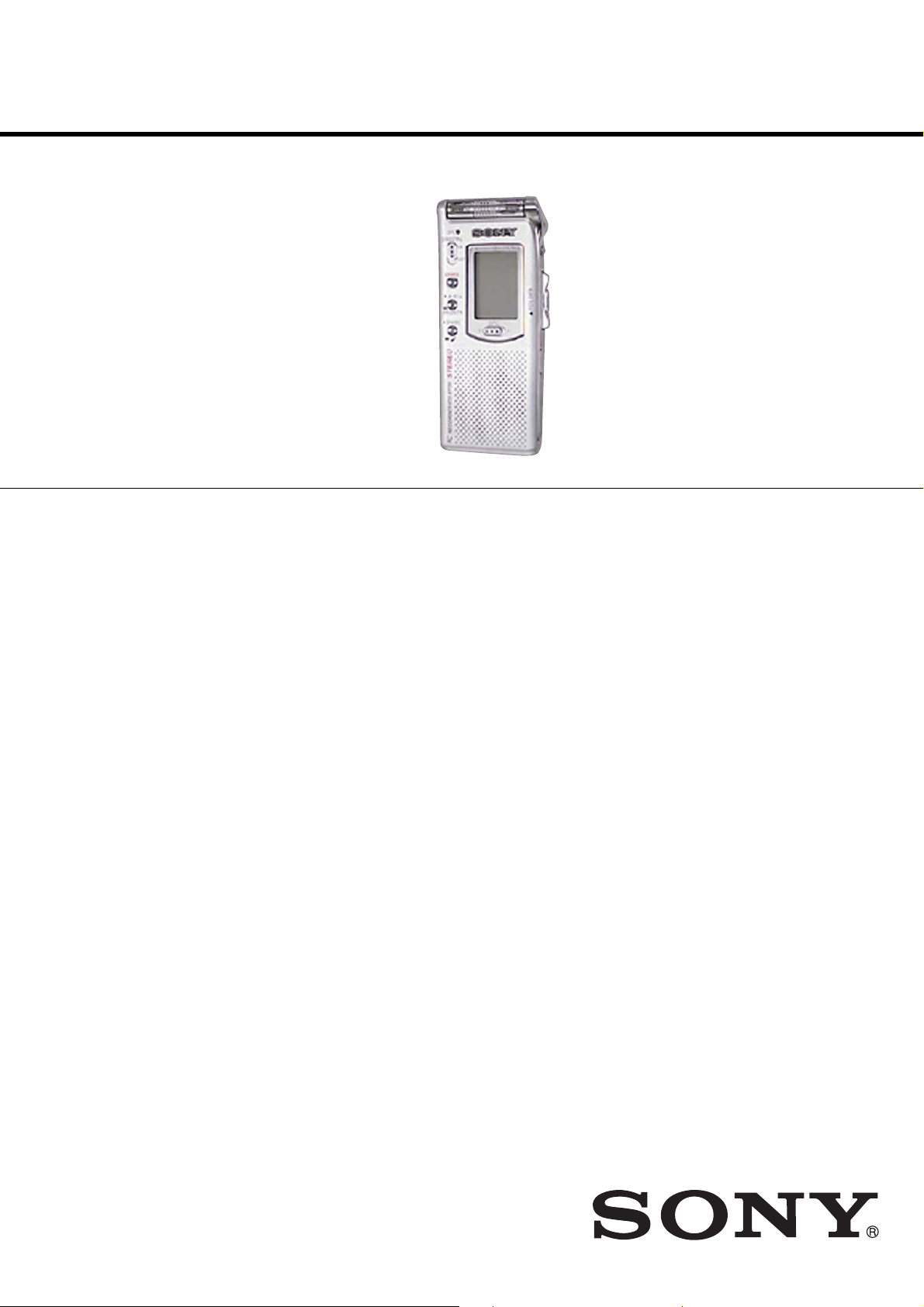
ICD-ST10/ST20
SERVICE MANUAL
Ver 1.2 2003. 07
Photo : ICD-ST10
SPECIFICATIONS
Recording media Built-in flash memory 32MB (ICD-ST20)/16MB
Recording time • ICD-ST20: 85 minutes (ST), 261 minutes (SP), 696
Speaker Approx. 28 mm (1
Power output 350 mW
Input/Output • Microphone jack (minijack, stereo)
Playback speed control +100% to -50% (DPC)
Power requirements Two LR03 (size AAA) alkaline batteries: 3 V DC
Dimensions (w/h/d)
Mass (incl. batteries) 75 g (2.65 oz)
Supplied accessories Stereo Ear Receiver × 1
Design and specifications are subject to change without notice.
(ICD-ST10), Stereo/Monaural recording
minutes (LP)
• ICD-ST10: 41 minutes (ST), 125 minutes (SP), 334
minutes (LP)
– input for plug in power, minimum input level
0.6 mV, 3 kilohms or lower impedance microphone
• Headphones jack (minijack, stereo)
–
output
• USB connector
(not incl. projecting parts and controls)
41.5 × 103.6 × 13.3 mm (1 11/16 × 4 1/8 × 17/
USB Connecting cable × 1
Application Software (CD-ROM) × 1
Carring Case x 1
LR03 (size AAA) alkaline batteries × 1*
*For the United States model only
for 8 - 300 ohms ear receiver
1
/8 in.) dia.
US Model
ICD-ST10
Canadian Model
ICD-ST10
AEP Model
ICD-ST10
UK Model
ICD-ST10
Tourist Model
ICD-ST10/ST20
Korean Model
ICD-ST20
in.)
32
9-877-313-03
2003G16-1
© 2003.07
IC RECORDER
Sony Corporation
Personal Audio Company
Published by Sony Engineering Corporation
Page 2

ICD-ST10/ST20
TABLE OF CONTENTS
1. GENERAL ·········································································· 3
2. DISASSEMBLY
2-1. Upper Lid Block Assembly ·········································· 4
2-2. F-SW Board ·································································· 5
2-3. MAIN Board ································································· 5
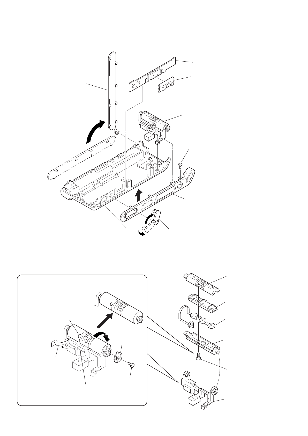
2-4. S-SW Board, Microphone Block Assembly ················· 6
2-5. Microphone Unit··························································· 6
2-6. The Cautions at the Time of a Microphone Block
Assembly ······································································ 7
3. TEST MODE······································································ 8
4. DIAGRAMS······································································ 11
4-1. Block Diagrams
– Main Section-1 –······················································12
– Main Section-2 –······················································13
– Panel/Power Section – ············································· 14
4-2. Printed Wiring Board – MAIN Board (Side A) – ······· 15
4-3. Printed Wiring Board – MAIN Board (Side B) –······· 16
4-4. Printed Wiring Board – F-SW Board – ······················· 17
4-5. Printed Wiring Board – S-SW Board – ······················· 18
4-6. Schematic Diagram – MAIN Board (1/5) – ··············· 19
4-7. Schematic Diagram – MAIN Board (2/5) – ··············· 20
4-8. Schematic Diagram – MAIN Board (3/5) – ··············· 21
4-9. Schematic Diagram – MAIN Board (4/5) – ··············· 22
4-10. Schematic Diagram – MAIN Board (5/5) – ··············· 23
4-11. IC Block Diagrams ····················································· 24
4-12. IC Pin Function Descriptions······································ 27
Flexible Circuit Board Repairing
•Keep the temperature of the soldering iron around 270°C during
repairing.
• Do not touch the soldering iron on the same conductor of the
circuit board (within 3 times).
• Be careful not to apply force on the conductor when soldering or
unsoldering.
Notes on chip component replacement
•Never reuse a disconnected chip component.
• Notice that the minus side of a tantalum capacitor may be damaged by heat.
✩Replacement of IC6001 used in this set requires a special tool.
• The voltage and waveform of CSP (chip size package) cannot be
measured, because its lead layout is diff erent from that of con v entional IC.
• Lead layouts
surface
Lead layout of
conventional IC
CSP (chip size package)
5. EXPLODED VIEWS
5-1. Upper Lid Block ························································· 32
5-2. Case Block ·································································· 33
6. ELECTRICAL PARTS LIST ······································· 34
Unleaded solder
Boards requiring use of unleaded solder are printed with the leadfree mark (LF) indicating the solder contains no lead.
(Caution: Some printed circuit boards may not come printed with
the lead free mark due to their particular size.)
: LEAD FREE MARK
Unleaded solder has the following characteristics.
• Unleaded solder melts at a temperature about 40°C higher than
ordinary solder.
Ordinary soldering irons can be used but the iron tip has to be
applied to the solder joint for a slightly longer time.
Soldering irons using a temperature regulator should be set to
about 350°C.
Caution: The printed pattern (copper foil) may peel away if the
heated tip is applied for too long, so be careful!
• Strong viscosity
Unleaded solder is more viscous (sticky, less prone to flow) than
ordinary solder so use caution not to let solder bridges occur such
as on IC pins, etc.
• Usable with ordinary solder
It is best to use only unleaded solder but unleaded solder may
also be added to ordinary solder.
2
Page 3
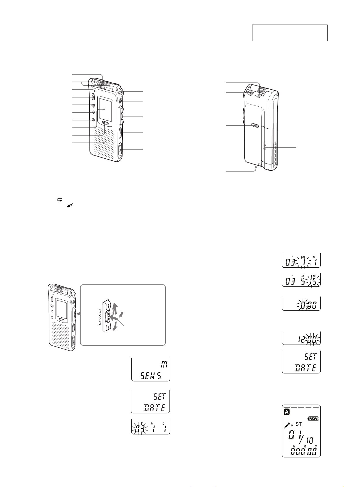
Index to Parts and Controls
2 Press the jog lever (x•B).
The month digits will flash.
3 Set the month and day in
sequence, then press the jog lever
(x•B).
The hour digits will flash.
5
Set the time.
1 Press the jog lever up or down
(>/.)toselect the digits of
the hour.
2 Press the jog lever (x•B).
The minute digits will flash.
3 Set the minute.
4 Press the jog lever (x•B).
The menu mode will be
displayed again.
Note
If you do not press the jog lever
(x•B) for more than one minute,
the clock setting mode is cancelled
and the window will return to
normal display.
6
Turnthe jog lever toward
MENU.
The window will return to normal
display.
1 If the unit is left unused for more than 3
seconds in the stop mode after the clock
is set, the display will show the current
time.
v
Refer to the pages indicated in parentheses for details.
Front
1
2
3
4
5
6
7
8
9
0
K
L
M
N
O
SECTION 1
GENERAL
Rear
ICD-ST10/ST20
This section is extracted from
instruction manual.
P
Q
R
T
1 Built-in microphone
2 Built-in microphone
3 OPE (operation) indicator
4 DIRECTNL (directional) switch
5 ERASE button
6 A-B
7 DIVIDE/
8 Display window
9 DPC ON/OFF switch
0
(repeat)/PRIORITY button
(bookmark) button
Speaker
Step 2: Setting the Clock
You need to set the clock to use the alarm function or record the date and
time.
Clock setting display appears when you insert batteries for the first time,
or when you insert batteries after the unit has been without batteries for a
certain period of time. In this case, proceed from step 4.
1
Turn the jog lever toward
MENU.
The menu mode will be displayed in
the display window.
2
Press the jog lever up or down
(>/.
3
Press the jog lever (x•B).
The date and time setting window is
displayed. The year digits will flash.
4
Set the date.
1 Press the jog lever up or down
) to select “SET DATE”.
(
>/.
the year.
Jog lever
Press up (>).
Press down (.).
) to select the digits of
K zREC (record) /REC
PAUSE button
L xSTOP button
M Jog lever
FOLDER/MENU/
.(review/fast backward)/
> (cue/fast forward)/
x• B (play/stop•enter)
N VOL (volume) +/– buttons
O USB connector
Turn toward MENU.
Press the center
(x•B).
S
P m (microphone) jack
Q i (headphones) jack
R HOLD switch
S DC IN 3V jack
T Battery compartment
3
Page 4
ICD-ST10/ST20
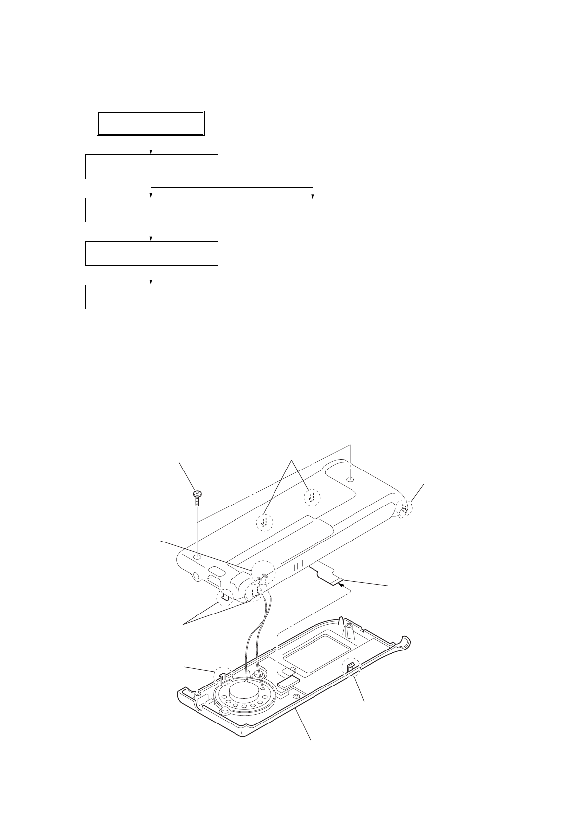
Note : Disassemble the unit in the order as shown below.
SET
UPPER LID BLOCK ASSEMBLY
SECTION 2
DISASSEMBLY
MAIN BOARD
MICROPHONE BLOCK ASSEMBLY
S-SW BOARD,
MICROPHONE UNIT
Note : Follow the disassembly procedure in the numerical order given.
2-1. Upper Lid Block Assembly
1
two tapping screws
(B 1.7
×
7)
two claws
F-SW BOARD
claw
3
Remove the
two solderings.
2
flexible board
two claws
claw
claw
4
upper lid block assembly
4
Page 5
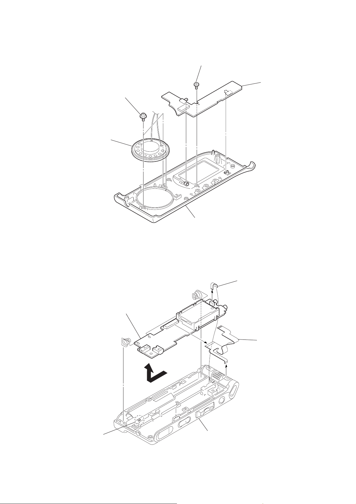
2-2. F-SW Board
d
2
(SP3001)
1
two screws
(1.7 × 2.5)
speaker (2.8 cm)
3
tapping screw
(1.7 × 2.5)
4
F-SW board
ICD-ST10/ST20
2-3. MAIN Board
5
MAIN board
4
5
upper lid sub block assembly
1
microphone unit
flexible board
2
flexible boar
3
claw
case block
5
Page 6
ICD-ST10/ST20
y
n
2-4. S-SW Board, Microphone Block Assembly
6
ornament (L)
5
S-SW board
4
button (5D)
7
microphone block assembl
2
pan tapping screw
(M 1.4 × 3)
2-5. Microphone Unit
4
Microphone part is turned in the direction of arrow A,
and it removes in the direction of arrow B.
screw hole part
B
A
2
click plate
3
1
lid (connector)
ornament (R)
7
microphone case
8
microphone cushio
9
microphone unit
q;
microphone cover
3
Microphone unit flexible
board is removed.
6
adhesive sheet
1
pan tapping screw
(M 1.4 × 2)
6
pan tapping screw
(M 1.4 × 4.5)
5
microphone base
Page 7
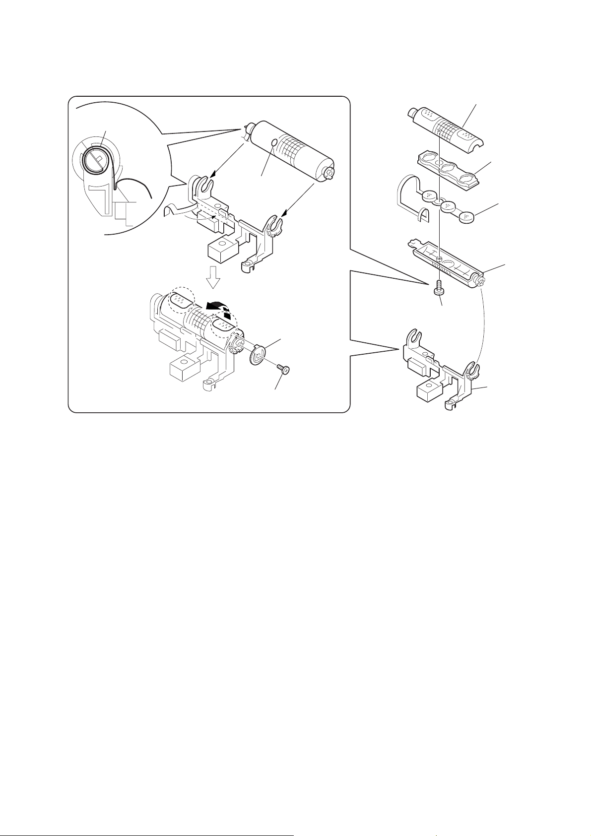
2-6. The Cautions at the Time of a Microphone Block Assembly
2
microphone unit
flexible board
It inserts in a microphone base.
screw hole part
3
It turns in the direction of an arrow.
microphone case
1
pan tapping screw
(M 1.4
×
4.5)
ICD-ST10/ST20
microphone cushion
microphone unit
microphone cover
click plate
4
pan tapping screw
×
(M 1.4
2)
microphone base
7
Page 8
ICD-ST10/ST20
SECTION 3
TEST MODE
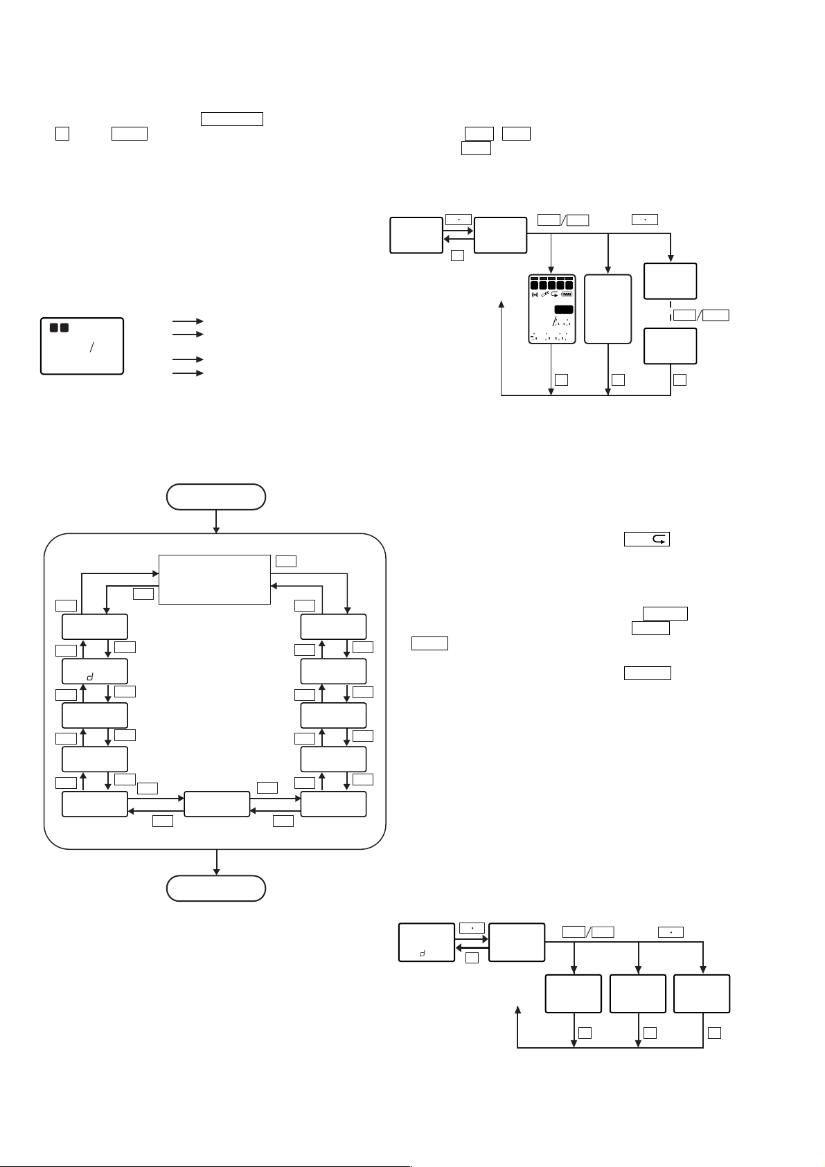
[Setting Method of the Test Mode]
To enter the test mode, turn on the HOLD . switch while pressing
the x key and VOL+ key at the same time with the power on.
[Exiting Method of the Test Mode]
Exit the test mode by turning off the power.
[Initial Status of the Test Mode]
When the test mode is set, the LCD display appears as shown below.
LCD display (Example)
A B
5A
102
01ST20
5A
102
01
ST20
Iris(DSP) version : 5A
SakuraR(CPU) version : 1.02
(In α version or β version, A or B is displayed)
LPEC ST version : 01
Model code : ST20
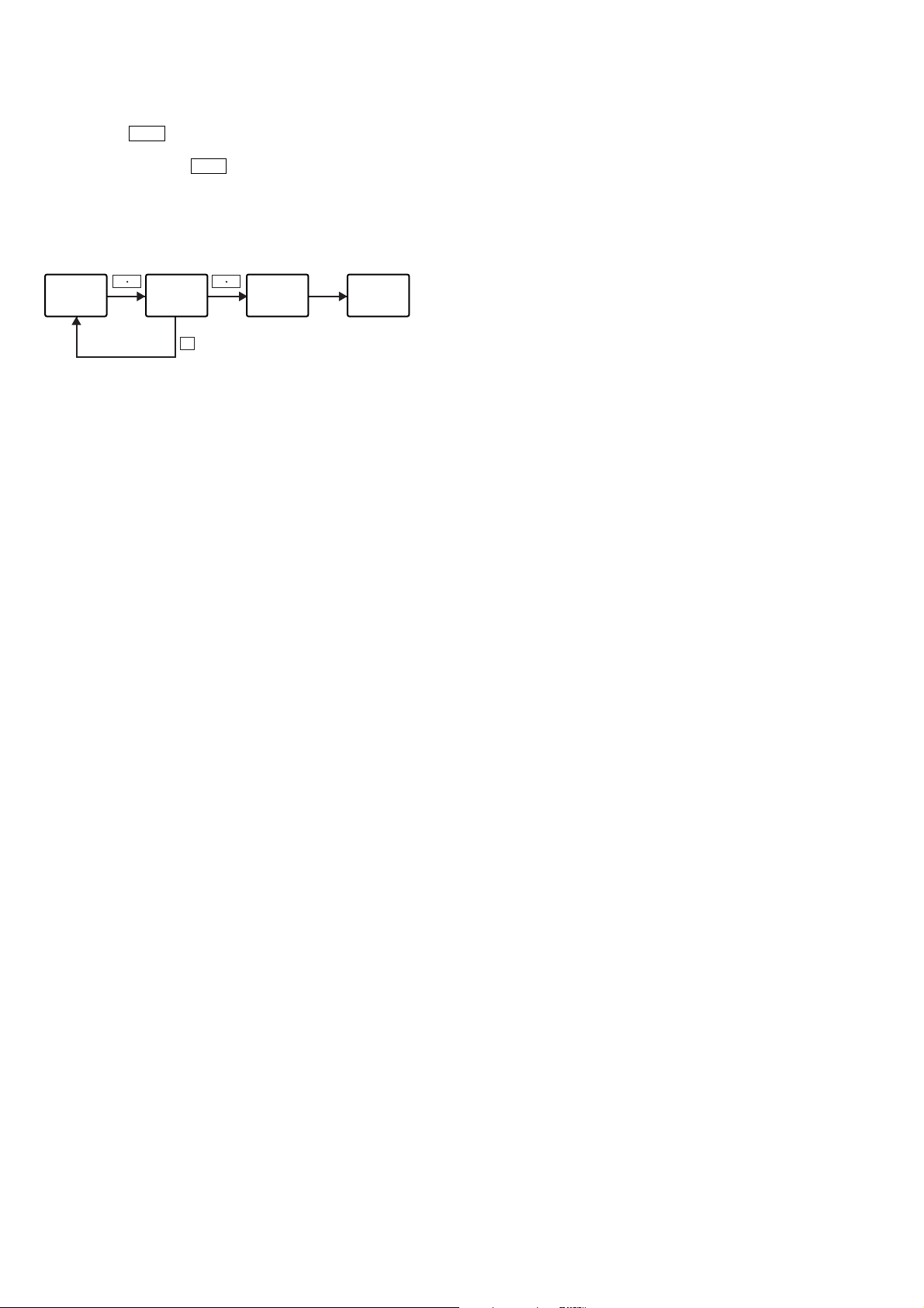
[Flow Chart of the Test Mode]
START
TEST MODE
>
.
.
>
>
>
>
>
RST
MENU
.
KEY
COUNT
.
USB
.
LED
.
BATTKEY
.
.
AU IO
.
.
.
LCD
SLEEP
BEEP
RTC
>
>
>
>
Initial status of test mode
Model code, LPEC ST,
>
F/W version display
>
.
[Operation in the Test Mode]
After entering the test mode, you can move within the test menu by
pressing the . / > key. You can move to the submenu by
pressing the x•B key. Then each test mode can be executed.
1. LCD test
• LCD is tested of all light-on and all light-off.
x B x B
LCD
x
ALL
LCD
:
OFF LCD
CHK LCD
ALL LCD
:
>
.
CBA
H
STSP
M
m
L
★
★
88
★
YM
888888
D E
REC
888
MM DS
LP
(select), (set)
(LCD off)
x x x
CHK
START
.
CHK
END
>
2. Audio test
Perform the through-playback and sine wave output.
• Contents of the submenu
DSP ST: DSP STEREO through mode
DSP MO: DSP MONO through mode
SIN: 1 kHz sine wave output mode
• Select the microphone sensitivity with the A-B
HtMtLtHtMt
...
switch.
•The VOR detection operation can be checked by the LED.
Sound: The red LED is turned on. No sound: The red LED is
turned off.
• MUTE can be set to “ON” or “OFF” with the ERASE key.
•The sound volume can be adjusted with the VOL+ key or
VOL- key during the audio test except the MUTE mode.
• In the directional microphone selection, ON/OFF of the
DIRECTNL switch is performed with the DIVIDE key.
DIRECTNL switch ON : The green LED is turned on.
OFF : The green LED is turned off.
• In the audio test mode the operation is performed according to
JACK detection.
•The microphone sensitivity, sound volume and MUTE (on/off)
are displayed on the LCD.
•The microphone sensitivity selection and the VOR test are
effective in the through-playback mode.
•The directional microphone selection is effective in the DSP
MONO through mode.
Tu rn off the power
(Extract the batteries or DC jack)
END
TEST MODE
DSP STEREO through mode / MIC : M / MUTE : ON / VOL-LEVEL : 12
DSP MONO through mode / MIC : H / MUTE : OFF / VOL-LEVEL : 23
1k sine wave output mode / MUTE : ON / VOL-LEVEL : 06 t "on / 06 / SIN"
x B
AU IO DSP ST
x
:
DSP MO
SIN
DSP ST
:
.
M
m
on
DSP ST
t "M / on / 12 / DSP ST"
t "H / oF / 23 / DSP MO"
>
(select), (set)
H
m
12
23
oF
DSP MO
x B
on
06
SIN
x x x
8
Page 9
ICD-ST10/ST20
FF
BATTBATT BATTBATT
DC jack
is inserted
DC jack
is extracted
x
x B
ON
LED
LED
x
x B
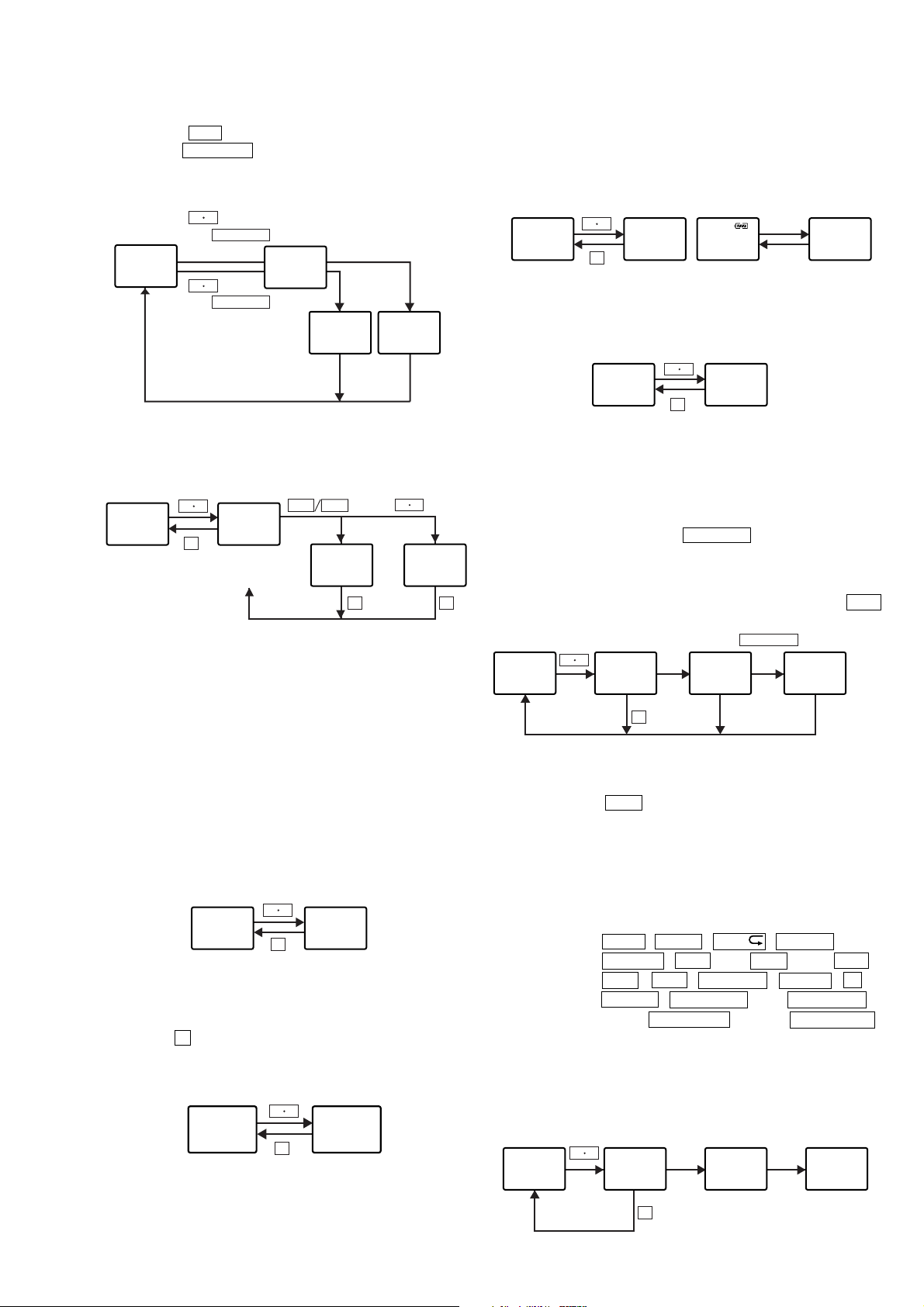
3. Sleep test
•Pressing the x•B key causes the set to enter the sleep state.
•When the HOLD . switch is ON, the LCD is turned off.
When OFF, the LCD is turned on.
•Press any keys to exit the sleep state.
x B
(with HOLD.
OFF status)
SLEEP
x B
(with HOLD.
ON status)
SOON
INSLEEP
(LCD OFF)
any keys any keys
4. Beep test
• Beep sound of 1.3 kHz or 2 kHz is output.
x B
BEEP 1.3K
x
2.0K
1.3K
:
:
.
(select), (set)
1.3K 2.0K
x x
x B
>
5. RTC test
•Perform the function test of the RTC and EEPROM.
(1) RTC EEPROM test
Confirmation of writing, reading (verifying) and erasing of
arbitrary data with the specified registers.
(2) RTC clock function test
Confirmation that RTC updates the time to the microcomputer
at one second interval.
• OK, NG judgement is performed to the test result.
When NG, it is displayed which device RTC or EEPROM
becomes NG.
(All OK : "RTC OK" / RTC NG : "RTC BAD" / EEPROM NG
: "EEP BAD")
x B
OK
x
RTCRTC
6. Key entry test
•When the any key is pressed, the entry key and the A/D converted
value (hexadecimal) of the two channel keys are displayed.
•When the x key is pressed, the A/D value of the key is displayed
while the key is depressed. When the key is released, the screen
returns to the test menu.
x B
oFF
KEYiFFKEY
x
7. Battery remaining power and DC IN test
•The detected A/D value (hexadecimal) of the battery remaining
power is displayed. When DC jack is inserted, the battery mark
on the LCD is turned off.
8. LED test
• LEDs (OPR: red and green, BL: green) are all turned on.
9. USB test
• When the menu starts the USB self-check, either presence or
absence of the Vbus is judged.
(Vbus is present: “ON VBUS”, Vbus is absent: “OFF VBUS”)
•The USB driver always works regardless of presence or absence
of the USB signal only when Vbus is available during the USB
test. At this time, turning on HOLD . causes the set to move
to the suspend state. Turning off the Vbus causes the set to return
to the test menu.
• In the menumode if the Vbus is supplied, any key will not work.
Therefore the Vbus will be supplied after surely pressing the x •B
key.
USB
x B
OFF
VBUS
Vbus
on
x
ON
VBUS
HOLD.
ON
LINK
cut Vbuscut Vbus
PC
Suspend
mode
10. Menu reset
•Pressing the x•B key causes the set to enter the menu
initialization standby state.
•When the following keys are all entered, the EEPROM
initialization (returning setting in the menu and user name to
default value) and formatting process (deleting all message files
in the flash memory) are executed. At the same time, the WakeUp
signal is checked, too.
Check keys: VOL- , VOL+ , A-B , ERASE ,
DIVIDE , DPC ON , DPC OFF , . ,
x•B , > , FOLDER , MENU , x ,
z REC , HOLD
OFF ,
DIRECTNL ON
.
ON , HOLD
, and DIRECTNL
.
OFF
• If all tests end in success, “-ALLOK-” is displayed. If initialization
in the EEPROM is NG, “INIT. NG” appears.
•Turn off the power to exit the test mode.
All keys
x B
RST
MENU
are entered
KEY
PUSH INIT
(blinking)
x
In the case that
the initialization
and reset operation
end correctly.
OK
ALL
9
Page 10
ICD-ST10/ST20
11. Key durable test
•Pressing the x•B key makes the count to "------" and sets test
standby status.
Once more pressing the x•B key makes the count to "000000"
and sets the key durable test.
In this mode any key input and slide switch operation are counted
and the number is displayed.
Turn off the power to exit this mode.
x B x B
KEY
COUNT
KEY
------
x
000000
Key durable
test
KEY
any keys or slide
switches operation
KEY
000001
10
Page 11
SECTION 4
DIAGRAMS
ICD-ST10/ST20
Note on Schematic Diagrams:
• All capacitors are in µF unless otherwise noted. pF: µµF
50 WV or less are not indicated except for electrolytics
and tantalums.
• All resistors are in Ω and 1/
specified.
f
•
• C : panel designation.
• A : B+ Line.
•Power voltage is dc 3V and fed with regulated dc power
•Voltages and waveforms are dc with respect to ground
•Voltages are taken with a VOM (Input impedance 10 MΩ).
•Waveforms are taken with a oscilloscope.
• Circled numbers refer to waveforms.
• Signal path.
✩Replacement of IC6001 used in this set requires a spe-
• The voltage and waveform of CSP (chip size package)
: internal component.
supply from DC IN jack (J5001).
under no-signal (detuned) conditions.
no mark : PB
[]: REC
Voltage variations may be noted due to normal production tolerances.
Voltage variations may be noted due to normal production tolerances.
F : PB
L : REC
cial tool.
cannot be measured, because its lead layout is different
from that of conventional IC.
: Impossible to measure
∗
4
W or less unless otherwise
Note on Printed Wiring Boards:
• Y : parts extracted from the conductor side.
• b : Pattern from the side which enables seeing.
The other layers’ patterns are not indicated.
Caution:
Pattern face side: Parts on the pattern f ace side seen from
(SIDE B) the pattern face are indicated.
Parts face side: Parts on the parts face side seen from
(SIDE A) the parts face are indicated.
• MAIN board is multi-layer printed board. However, the
patterns of intermediate-layer have not been included in
the diagram.
✩Replacement of IC6001 used in this set requires a spe-
cial tool.
• Lead layouts
surface
Lead layout of
conventional IC
CSP (chip size package)
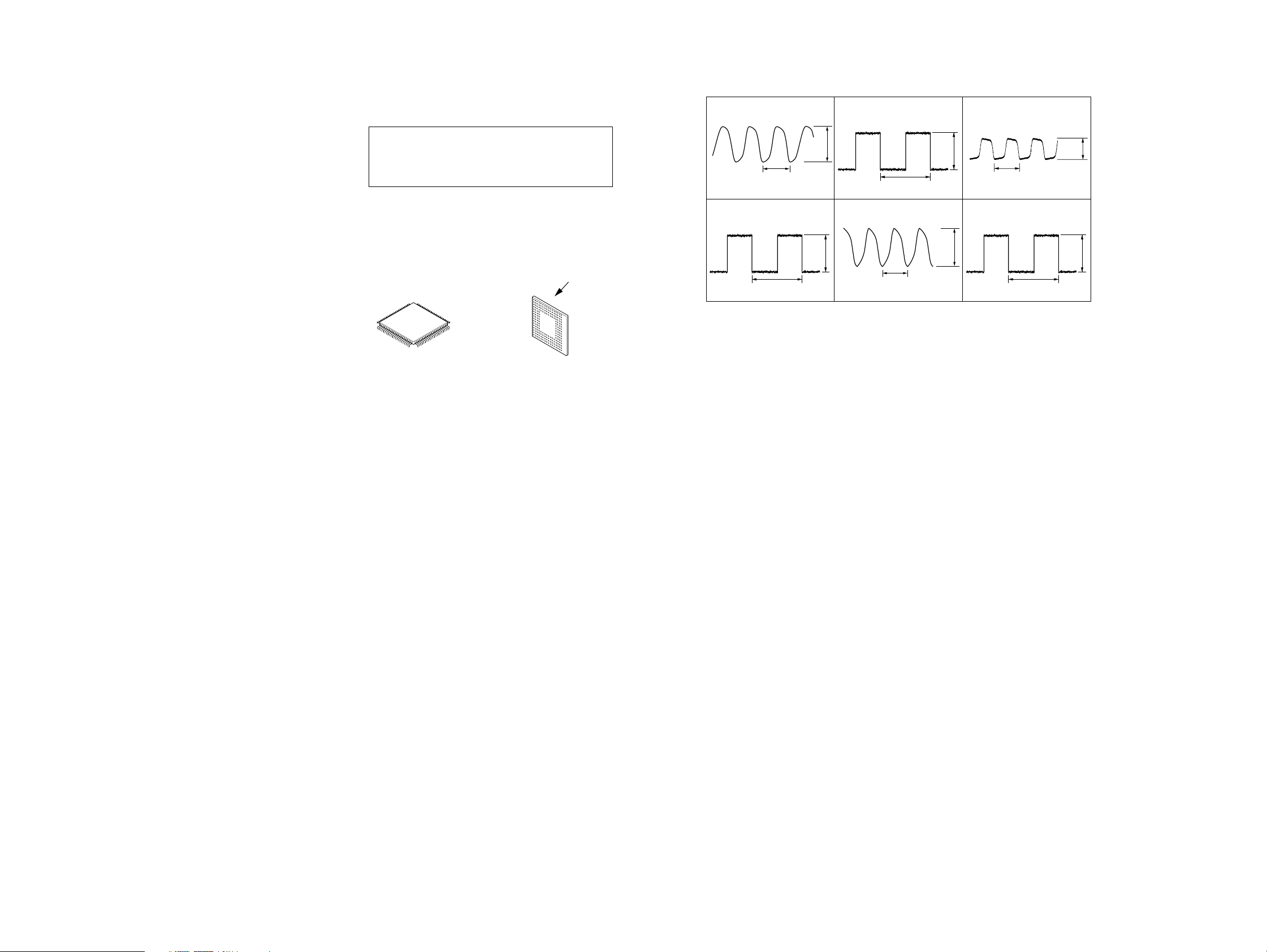
• WA VEFORMS
1
IC6003 3 (XXT)
88.5 ns
1 V/DIV, 40 ns/DIV
2
IC6003 1 (FOUT)
1 V/DIV, 40 ns/DIV
88.5 ns
3.3 Vp-p
4.1 Vp-p
3
IC3004 6 (MCLK)
1 V/DIV, 40 ns/DIV
4
IC7003 <z/, (XTAL)
1 V/DIV, 100 ns/DIV
88.5 ns
244 ns
4.1 Vp-p
3.4 Vp-p
5
IC8001 qd (X OUT)
(When the USB is connected)
8.33 ns
1 V/DIV, 40 ns/DIV
6
IC7004 5 (FOUT)
1 V/DIV, 10 µs/DIV
3.7 Vp-p
3.2 Vp-p
30.5 ns
1111
Page 12
ICD-ST10/ST20
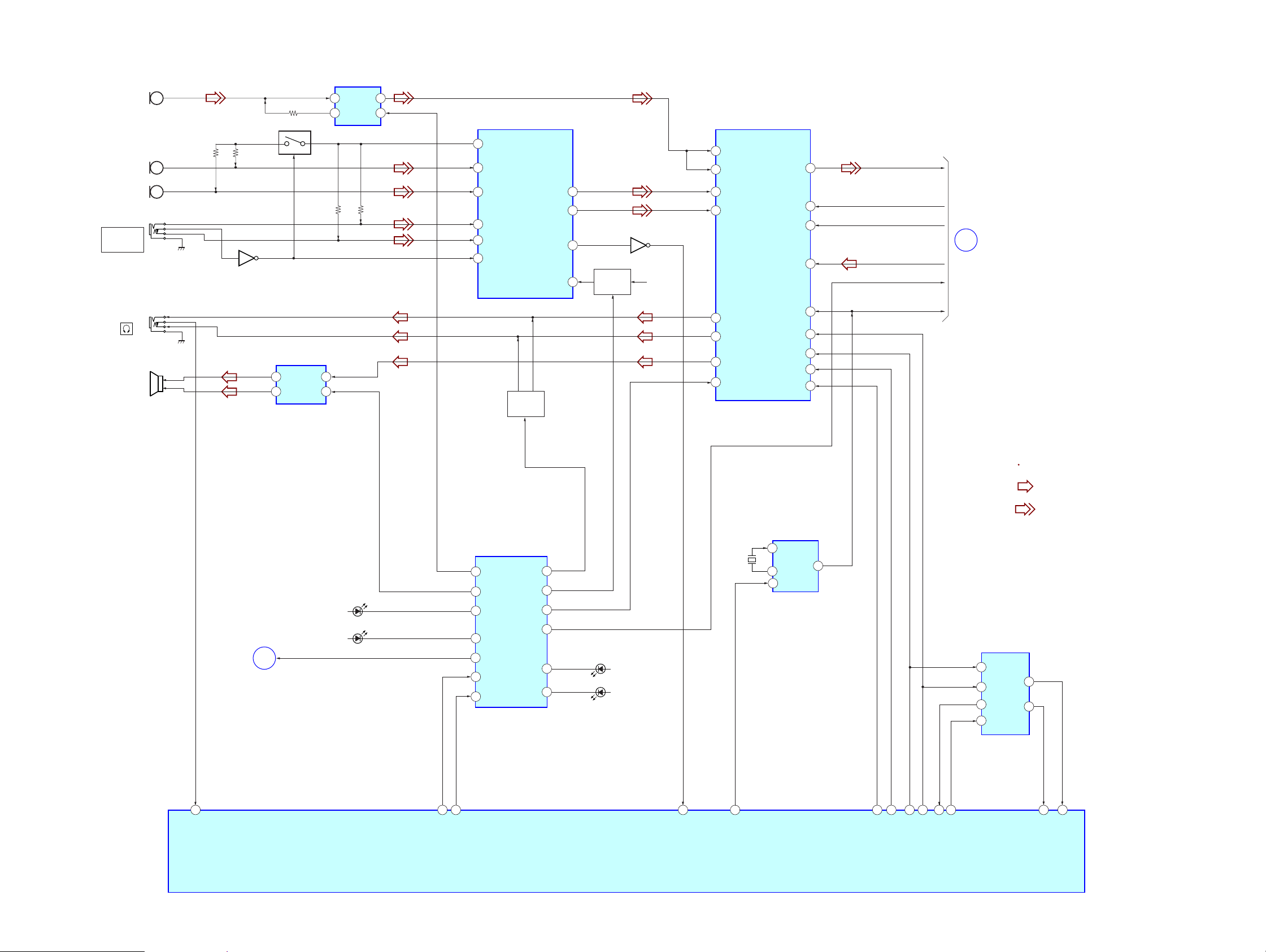
4-1. Block Diagrams – Main Section-1 –
MIC1
(ZOOM)
MIC2
(L-CH)
MIC3
(R-CH)
J3001
m
PLUG IN POWER
Q3002
Q3004
4
2
IC3002
MIC AMP
IN+
REG
OUT
STBY
6
3
26
6
24
29
2
1
MICVCC
INTINL
INTINR
EXTINR
EXTINL
CTL1
IC3001
MIC AMP
OUTL
OUTR
INT/EXT
VCC
IC3004
ADC, DAC, HEADPHONE AMP
AINR2
25
STDO
BICK
LRCK
SDTI
9
7
5
8
AINL2
26
13
17
Q3001
16
Q5008
7
B+ SWITCH
AVDD
AINL1
28
AINR1
27
STDO
BCLK
LRCK
A
SO
XRST
J3002
SP3001
(SPEAKER)
B
POWER AMP
5
VO1
8
VO2
D902
(OPR)
(REC/PB)
XBATTEN
IC3003
XSHUT-
DOWN
4
-IN
1
RED(REC)
GREEN(PB)
13
8
6
5
12
3
2
SI/PO DRIVER
MONOMIC
SPAMP
XREDLED
XGRLED
XBATTEN
CLK
DATA
IC7001
XADAPDN
XDSPRST
Q3003
MUTE
HPMUTE
XSTMIC
XLIGHT1
XLIGHT2
MCLK
CDTI
CCLK
MIN
CSN
IC6003
CLOCK GEN
XT
FOUT
XXT
XCONT
6
4
3
18
2
1
HPR
14
HPL
15
MOUT
17
PDN
1
X6001
11.2896MHz
5
15
7
9
11
4
14
D7002
(LCD PANEL LIGHT)
D7003
3
4
MCLK
IC7004
REAL TIME CLOCK
CLK
9
XIRQ
DI
7
DO
8
FOUT
CE
10
Signal path
: PB
: REC
3
5
46
HPJACK
115
SPICLK
45
SPIDATA
IC7003 (1/3)
CPU
XMICJACK
DSPSYSCLK
102
18
BEEP
XADACS
100
AUSCK
99
98
AUSOT
10112116
AUSIN
RTCCS
13
X0A32K
111
XRTCINTR
1212
Page 13

– Main Section-2 –
ICD-ST10/ST20
DSPCVDD
A
STDO
BCLK
LRCK
SO
XRST
MCLK
IC5005
VOLTAGE
DETECT
IC6001
DSP
ADASI
45
40
BCLK
LRCLK
47
SO
35
138
XRST
MCLK
46
150
CLKIN
12
TSO
TSCK
TSOEN
TSIEN
TSIOEN
TSI
FMSDIO
FMSCK
XFMWP
XFMCS
48
49
50
55
158
52
160
157
11
12
IC6004
4
FLASH MEMORY
5
2
6
3
1
2
IC6002
SDI
SDO
SCK
XWP
XCS
119
1
118
120
IC7003 (2/3)
CPU
DSPSIN
DSPSCK
DSPSIOEN
DATA0-DATA7
DSPSOT
USBADR0 - USBADR6
FLMRB
FLMCLE
XFLMALE
XFLMCS0
XFLMRE
22
2
21
11
20
19
3-10
24-30
IC7002
FLASH MEMORY
R/B
7
CLE
16
ALE
17
XCE
9
RE
8
WEXFLMWE
18
WPXFLMWP
1923
29-32,
I/O1-I/O8
41-44
IC8001
USB CONTROLLER
D0 - D7
23-30
40,
A0 - A6
17-22
D8002
Q7002
SWITCH
IC8003
+3.5V
REG
CN7001
USB
KEYINH
23
DDCOUT
VBUS
C
D
E
Signal path
: PB
: REC
REQ
159
Q7005
X7001
4.096MHz
104
107
108
DSPIFREQ
XTALIN
XTAL
XUSBCS
XINTUSB
XUSBVBUS
XUSBLWR
XUSBRD
XUSBRST
RX
TX
MOD2
WAKEUP
31
109
110
34
32
33
95
96
87
103
Q7003
WAKEUP
SWITCH
CS
45
INT0
42
INT1
11
LWR
44
RD
43
46
RST
Q7004
VBUS
D+
TRON
XIN
XOUT
5
3
D-
4
6
14
13
X8001
12MHz
1
VBUS
2
D-
3
D+
4IN
WAKEUP
F
1313
Page 14

ICD-ST10/ST20
– Panel/Power Section –
S903,904,
FUNCTION
S910
SEESAW
KEY
906,907
KEY
LIQUID
CRYSTAL
DISPLAY
MODULE
49-74,
77-82
83-86
40
SEG0 - SEG31
COM0 - COM3
KEYIN0
IC7003(3/3)
CPU
XCPURST
XFLMPWR
DDCOUT
D
IC7005
90
97
RESET
32
Q7001
FLMVCC
(IC7002)
B+
SWITCH
DIRECTNL
S7001
HOLD
S901
S902
DPC
S905,
908,909
FUNCTION
KEY
WAKEUP
F
KEYINH
C
ON
OFF
ON
OFF
ON
OFF
41
42
44
112
KEYIN1
MICSEL
XDPCSW
HOLDSW
DSPPWR
BATT
XDCINDET
117
113
DSPEVDD
(IC6001, 6002, 6003)
VBUS
E
39
XBATTEN
B
Q5006,5007
B+
SWITCH
Q5001
SWITCH
DDCOUT(3.1V)
AVDD(2.9V)
SWITCH
Q5012
IC5001
+2.9V
REG
4
DSPCVDD(1.6V)
IC3003 VDD
DDCOUT
(3.1V)
15
3
4
6
IC5003
DC/DC CONV.
FB1
EXT1
PWM1
EN2
FB2
EXT2
L5002
D5004
D5003
Q5002
SWITCH
1
108
Q5003
SWITCH
L5001
VBATT
Q5005
DC DET
IC5004
B+
SWITCH
IC5002
VOLTAGE
DETECT
Q5010, 5011
SWITCH
31
D5005
Q5009
DRY BATTERY
SIZE "AAA"
(IEC DESIGNATION LR03)
2PCS, 3V
J5001
DC IN 3V
1414
Page 15

ICD-ST10/ST20
4-2. Printed Wiring Board – MAIN Board (Side A) –
12
S
(SIDE A)
S
45
1
85
2
IC5002
Q5013
3
14
A
MAIN BOARD
B
J5001
C
D
3
EXCEPT:ST20
8
E
1
E
F
• : Uses unleaded solder.
3456789
IC5005
4
3
S
5
IC5001
1
IC5003
S
S
C5012
R5012
ST20
3
IC6001
CSP(Chip Size Package)
C6002
IC6002
ST20
3
IC6003
4
1
6
S
OFF
HOLD
ON
S7001
IC3003
C1008
IC3001
IC3004
E
S
S
45
13
C2009
IC3002
2
1
4
IC6004
E
S
1-687-788-
(11)
J3002
i
J3001
m
PLUG IN POWER
11
• Semiconductor
Location
Ref. No. Location
D5002 C-2
D5003 D-3
D5004 D-3
D5005 D-2
D5007 E-2
D5009 D-2
IC3001 C-7
IC3002 E-7
IC3003 C-6
IC3004 D-6
IC5001 C-3
IC5002 B-2
IC5003 D-3
IC5005 B-3
IC6001 C-5
IC6002 E-5
IC6003 E-5
IC6004 E-7
Ref. No. Location
Q3001 D-7
Q3002 B-8
Q3004 E-8
Q5001 C-6
Q5002 D-3
Q5003 E-3
Q5005 C-1
Q5006 E-6
Q5007 E-6
Q5008 B-6
Q5009 C-1
Q5010 B-2
Q5011 C-1
Q5012 B-3
Q5013 E-2
1515
Page 16

ICD-ST10/ST20
4-3. Printed Wiring Board – MAIN Board (Side B) –
12
A
B
MAIN BOARD
SP3001
(SPEAKER)
(SIDE B)
DRY BATTERY
(IEC DESIGNATION LR 03)
SIZE "AAA"
2PCS,3V
C
D
IC8001
E
1
5
F
• : Uses unleaded solder.
3456789
S
S
R7011
1
2
IC8003
3
R7048
IC7001
R7047
IC7002
A
CN7004
TO
F-SW
BOARD
CN901
(Page 17)
TO
S-SW
B
BOARD
CN902
(Page 18)
181
4
3
2
1
MICROPHONE
UNIT
MIC2
MIC1
ZOOM
MIC3
Lch
Rch
IC7003
1
2
IC7005
IC7004
3
(LCD PANEL LIGHT)
1
5
S
E
(LCD PANEL LIGHT)
E
136
1
45
1-687-788-
CN3001
8
2
4
11
(11)
• Semiconductor
Location
Ref. No. Location
D7002 C-9
D7003 E-9
D7004 C-8
D8001 F-3
D8002 F-2
IC7001 F-3
IC7002 E-5
IC7003 C-3
IC7004 C-8
IC7005 E-8
IC8001 D-2
IC8003 F-3
Q3003 E-9
Q7001 C-4
Q7002 D-3
Q7003 C-8
Q7004 C-8
Q7005 D-8
CN7001
USB
LCD
TO
1616
Page 17

ICD-ST10/ST20
4-4. Printed Wiring Board – F-SW Board –
F-SW BOARD
• : Uses unleaded solder.
(SIDE A)
S901
ON OFFDIRECTNL
ON
OFF
F-SW BOARD
(SIDE B)
OPE
S904
ERASE
S903
A-B PRIORITY
S902
ON OFF
DPC
ON
OFF
S905
DIVIDE
10
(bookmark)
11
1-687-789-
(11)
CN901
1-687-789-
11
(11)
A
(Page 16)
TO
MAIN
BOARD
CN7004
1
1717
Page 18

ICD-ST10/ST20
4-5. Printed Wiring Board – S-SW Board –
• : Uses unleaded solder.
S-SW BOARD
(SIDE A)
S-SW BOARD
S909
REC/REC PAUSE
STOP
(SIDE B)
B
TO
MAIN
BOARD
CN7004
(Page 16)
CN902
18
1-687-790-
12
(12)
VOL
VOL
1-687-790-
S910
FOLDER
12
(12)
MENU
PUSH PLAY/STOP(ENTER)
1818
Page 19

ICD-ST10/ST20
4-6. Schematic Diagram – MAIN Board (1/5) –
Q3004
3LP01S-TL
FB2001
FB3001
FB3004
FB1002
TP3004
R3027
1M
R2002
4.7k
R1009
1k
2.2k
2.2k
R2016
CN3001
MIC2
LCH
MIC1
ZOOM
MIC4
RCH
J3001
PLUG IN POWER
J3002
SP3001
5P
TP1003
TP3005
TP3003
TP2003
TP3002
TP3001
R1016
FB1001
FB2002
FB3002
JC3001
• See page 11 for Waveforms. • Refer to page 24, 25 for IC Block Diagrams.
R3003
2.2k
C3001
4.7k
R1001
47
R1002
2.2k
C1012
0.1
C1016
47 6.3V
0.01
0.01
C1001
C1003
0.1
Q3002
UN9214J-(K8).SO
R2012R1012R2009
1k1k1k
C1002
R2010
R1010
0.1
C2005
C1005
0.1
R2004 C2009
R2005
R2006
C2006
0.047
0.047
C1006
4.7k
R1004
1k
R1005
C1008
R1003
C1007
R3015
22k
1k 0.022
C2007
0.047
4.7k
0.047
C2008
4.7k
R2007
10k
R1006
10k
4.7k
0.047
0.047
R5018
1M
0.022
C3016
0.022
C1011
UN9214J-(K8).SO
C3004
10
6.3V
Q3001
R3029
0
C2004
C1004
0.01
220k
C2003
0.47
0.47
6.3V
6.3V
10
10
C3028
C3003
Q5008
3LP01S-TL
0.01
C2001
0.01
R2003
22k
R2013
0.1
R3005
C2002
4.7
4.7
R3004
100k
IC3001
LA7473V-TLM
R1013
22k
C1015
0.001
100k
IC3003
R2015
0.001
C2015
10k
R1015
10k
LM4903
R2001
2.2k
0.1
C2016
C2012
6.3V
R3007
100k
R3009
22k
C3005
R3008
0.1
10k
C2013
C1013
C3007
R3010
C3008
0.1
0.1
C3009
0.1
2.2k
R3012
1
47k
0.1
R3022
IC3002
NJM2781RB1(TE1)
100
C3030
C3027
10 6.3V
C3010
1
1
(Page 23)
2.2 6.3V
C3017
C3018
C3019
C3022C3021
C3020
0.10.1
10 6.3V
0.1
0.1
IC3004
AK4566VN-L
R3023
0
C3023
0.01
R3016
220
R3017
100k
C3024
0.1
0.1
R3020
C3025
10
C3026
0.001
Q3003
NTHD5904T1
C3011
C3012
6.3V
R3018
100k
C3013
220p
R3013
220k
R3014
100k
C3015
R3030 100k
0.47
0.1
10
(Page 20)
C7023
0.01
470k
R7043
(Page 23)
R3024
470k
C7001
0.1
R7003
R7002
D7003
CL-196SYG
100
100
D7002
CL-196SYG
(Page 22)
IC7001
BU2090FS-E2
(Page 21)
(Page 22) (Page 21) (Page 22)
1919
Page 20

ICD-ST10/ST20
4-7. Schematic Diagram – MAIN Board (2/5) –
C7022
1
Q7001
NDS356AP
R7010
R7040
470k
10k
R7011
470k
(Page 19)
R7009
1M
R7044
TP7014
1k
• See page 11 for Waveforms. • Refer to page 26 for IC Block Diagrams.
IC7002
K9F2808U0C-YCB0T : EXCEPT ST20
K9F5608U0B-YCB0T : ST20
IC7002
C7003
C7004
0.1
C8001
0.1
IC8001
M66291GP-2
C8005
X8001
C8003
12MHz
8p
0.1
R8006
C8002
100k
R8003
R8005
470k
R8002R8001
470k470k
1M
R8004
C8004
0.001
100k
R8009
R8008
8p
R8022
470
220
IC8003
XC62FP3502MR
D8001
RB520S-30TE61
C8006
0.1
R8007
470k
R8010
100k
R8011
100k
R8012
100k
R8013
2.2k
R8015
22
R8016
22
C8007
0.1
0
R8021
1SS352
4.7k
D8002
R8020
C8009
4.7 10V
1
C8010
TP7002
R7048
FB7001
FB7002
1k
0H
1
R7039
1k
R7047
1k
CN70010.1
0H
5P
76
(Page 23)
2020
Page 21

ICD-ST10/ST20
4-8. Schematic Diagram – MAIN Board (3/5) –
• Refer to page 25 for IC Block Diagrams.
D5004
CRS02(TE85L)
Q5003
XP152A12CBMR
L5002
R5009
470k
C5012
100p
R5012
2.2k
R5010
150k
(Page 19)
ST20
C5009
0.1
C5014
6.3V
47
C5005
10
6.3V
IC5001
R1160N2918-TR-FA
TP5006
TP5004
C5020
0.1
IC5005
XC61CS23XXNR
(Page 19)
J5001
W5001
W5002
D5009
MAZS120008S0
D5007
MAZS120008S0
TP5001
TP5008
C5003
47 10V
TP5002
C5004
0.1
C5006
0.1
TH5001
THERMISTOR
MA2ZD02001SO
TP5003
D5002
L5001
C5007
1
IC5002
S1F77600
IC5003
XC95028092AR
XP151A12A2MR
(TE85L)
Q5002
D5003
CRS02
C5011
22p
R5007 R5008
470k 680k
R5005
470k
D5005
MA2ZD02001SO
T5001
R5006
680k
Q5011
3LP01S-TL
R5021
Q5009
470k
SW
NTHD5904T1
R5025
1M
Q5013
NTHS5445T1
R5022
470k
R5024
2.2M
Q5010
3LN01S-TL
R5011
2.2k
EXCEPT
: ST20
C5017
47
10V
Q5005
2SC4617TL-Q2
1k
R5013
C5018
10V
47
TP5009
TP5007
Q5012
2SK3019TL
SWITCH
R5014
100k
C5016
10V
Q5007
R5017
1M
NOS356AP
C5022
4.7
10V
TP5010
(Page 22)
R5023
0
TP5005
Q5006
3LN01S-TL
R5016
470k
C5021
33
R5015
470k
0.1
75
(Page 23)
C5010
0.1
(Page 22)
2121
Page 22

ICD-ST10/ST20
4-9. Schematic Diagram – MAIN Board (4/5) / Switch Section –
(Page 19)
(Page 19)
TP7006
TP7007
(Page 21)
(Page 19)
TP6012
N6T
470k
25P10-AVM
M
R6004
IC6002
R3028
TP6013
100k
R6009
220
TP6011
0.1
C6003
R6003
470k
C6001
1
C6002
1
470k
R6001
ST20
C6015
47p
470k
R6002
• See page 11 for Waveforms. • Ref er to page 25 for IC Bloc k Diagr ams . • See page 27 f or IC Pin Function Description.
TP6001
TP6002
TP6004TP6003
R6014R6013
100k100k
RB6002
100k
100k
R6006
100k
R6007
IC6001
RB6001
100k
R6005
100k
470k
R6010R6008
R6011
470k470k
470k
R6012
R6015
0.001
C6007
100k
100k
100k
R6018
017
100k
6016
R
R6
TP6005
TP6006
C6014
100p
100k
C6010
R6019
TP6007
TP6008
TP6009
TP6010
R6025
11.2896MHz
C6009
C6006
0.1
100k
R6020
100k
R6021
0.1
IC6004
TC7504FU(TE85R)
T(TE1)
6366AF
JU
N
IC6003
470
R6022
47
X6001
5p
C6008
5p
R7006
2.2k
R7007
R7008
1k
1k
CN7004
(Page 23)
C902
C901
4700p
S918 R911
33k
CN902
8P
R910
18P
CL-165HR/YG-D-T
CN901
10P
R909
22k
R908
22k
R904
4.7k
R903
3.3k
D902
OPE
4700p
FOLDER
MENU
PUSH PLAY/S TOP(ENTER)
33k
REC/REC PAUSE
S909
ERASE
S908
STOP
S907
VOL
S906
VOL
S905
(book mark)
DIVIDE
S904
S903
PRIORITY
S902
ON / OFF
S901
DIRECTNL ON / OFF
R907
R906
4.7k
3.3k
R905
2.2k
R913
4.7k
R912
1k
(Page 21)
(Page 23)
2222
Page 23

ICD-ST10/ST20
4-10. Schematic Diagram – MAIN Board (5/5) –
(Page 19)
(Page 19)
(Page 22)
75
(Page 21)
• See page 11 for Waveforms. • Refer to page 26 for IC Block Diagrams. • See page 30 for IC Pin Function Description.
(Page 19)
76
R7027 100k
R7028 0
D7004 1SS352
R7030
100
16
10V
C70
47
R7025
470k
RX-4591CF
7004
IC
C7017
0.1
HOLD
S7001
R7012
X7001
4.096MHz
C7009
TP7010
470k
R7015
1k
R7019
100p
0
R7023
470k
C7010
0.1
R7041
0
0
R7042
0
R7026
R7029 R7031 R7034
100k 100k 100k
Q7004
UN9214J-(K8).SO
C7019
100p
R7038
TP7001
TP7003
100k
UN9214J-(K8).SO
IC7005
R3130N28EA-TR
Q7005
C7021
0.1
(Page 22)
TP7012
C7005
TP7013
R7001
0.1
C7020
1000p
TP7004
CN7002
36P
1M
IC7003
MB91F233
C7011
0.1
1k
7022
R
C7014
0.1
C7012
0.1
C7013
0.1
R7032
100k
C7015
1000p
R7033
100k
Q7002
3LP01S-TL
R7014
R7013
C7006
0.1
C5001
0.1
R5001
100k
R5002
33k
Q5001
3LP01S-TL
R5003
470k
R7045 470k
R7016 220k
R7046 470k
10k
TP7008
TP7009
10k
1k
7020
R
Q7003
3LP01S-TL
C7018
0.1
2323
Page 24

ICD-ST10/ST20
4-11. IC Block Diagrams
IC3001 LA7473V-TLM (MAIN BOARD)
CTL-2
EXT MIC
AMP R
EXT MIC
DET
EXT MIC
AMP L
1 2 3 4 5 6 7 8 9 10 11 12 13 14 15
CTL-1
EXT IN-L
EXTNF1L
EXTNF2L
MIC
VCC
RIPPLE
FILTER
MIC VCC
RF
HPFSW
INT IN-R
VCC
INT IN-L
INTNFR
INT MIC
INT MIC
INTNFL
AMP R
AMP L
GND
INTOUTR
MIXINR
INTOUTL
MIXINL
MIX
AMP R
MIX
AMP L
MIXOUTR
192021222324252627282930
OFF
OFF
MIXOUTL
HPF IN-R
ON
ON
HPF IN-L
EXT
EXT
INT
INT
OUTPUT
AMP R
OUTPUT
AMP L
OUT-R
BIAS
OUT-L
BIAS
EXTNF2R
EXTNF1R
EXT IN-R
INT/EXT
161718
SIT/MONO
IC3003 LM4903MMX/NOPB (MAIN BOARD)
VDD/2
XSHUTDOWN
BYPASS
+IN
1
BIAS
2
3
4
-IN
AV=-1
8
VO2
7
GND
6
VDD
5
VO1
IC3002 NJM2781RB1 (MAIN BOARD)
NOISE
REG
STBY
IN+
1
2
3
4
REG
8
GND
7
V+
6
OUT
5
IN-
IC3004 AK4566VN-L (MAIN BOARD)
HPR
15
HPL
MUTET
MOUT
MIN
RIN
LIN
VREF
16
17
18
19
20
21
AINL1
AINL2
AINR1
AINR2
HP AMP
MOUT
HVDD
HVSS
IPGA
DVSS
ADC
DAC
DVDD
BOOST
SDTO
IPGA & ADC
HPF
DAC
DATT
SDTI
814 13 12 11 10 9
AUDIO I/F
CONTROLLER
CONTROL
REGISTER
7
BICK
6
MCLK
5
LRCK
4
CDTI
3
CCLK
2
CSN
1
PDN
VREF
VCOM
VCOM
AVSS
AVDD
AINR2
AINL2
AINR1
2822 23 24 25 26 27
AINL1
2424
Page 25

IC5003 XC9502B092AR (MAIN BOARD)
ICD-ST10/ST20
EXT1
VDD
FB1
PWM1
EN1
1
2
3
4
5
PWM/PFM
CONTROLLER1
PWM
COMPARATOR1
ERROR AMP1 ERROR AMP2
VREF1=0.9V
WITH SOFT START1,
EN1
EN1 TO
INTERNAL CIRCUIT
RAMP WAVE
GENERATOR1
GENERATOR
CONTROLLER2
RAMP WAVE
GENERATOR2
OSC
PWM/PFM
IC6003 NJU6366AF1(TE1) (MAIN BOARD)
XXT
VDD
PWM
COMPARATOR2
VREF1=0.9V
WITH SOFT START2,
EN2
EN2 TO
INTERNAL CIRCUIT
FOUT
13 2
10
EXT2
9
GND
8
FB2
7
PWM2
6
EN2
RF
1/2 1/2 1/2
CG CD
ABC D
XT
XCONT
IC7001 BU2090FS-E2 (MAIN BOARD)
VDD
HPMUTE
XLIGHT2
MONOMIC
XBATTEN
OUTPUT
BUFFER
(OPEN DRAIN)
CONTROL
CIRCUIT
12 BIT
SHIFT
REGISTER
12 BIT
STORAGE
REGISTER
16 15 14 13 12
3-STATE
BUFFER
64 5
XDSPRST
10
11
VSS
XFLMPWR9XADAPDN
2 3 5 6 7 8
1
CLK
VSS
DATA
4
XLIGHT1
XGRLED
XREDLED
SPAMP
XSTMIC
25
Page 26

ICD-ST10/ST20
IC7004 RX-4591CF (MAIN BOARD)
32.768kHz
1
VDD
DIVIDER
FOUT
CONTROLLER
INTERRUPTS
CONTROLLER
BUS
INTERFACE
CIRCUIT
FOE
XIRQ
FOUT
OSC
2
3
DI
4
T1
5
DO
CLK
CE
IC8001 M66291GP-2 (MAIN BOARD)
CLOCK
AND
CALENDAR
TIMER
REGISTER
ARARM
REGISTER
CONTROL
REGISTER
AND
SYSTEM
CONTROLLER
CE
CLK
DO
DI
10
CE
9
CLK
8
DO
7
DI
6
GND
CVDD
GND
VBUS
TRON
TEST
DACK1
DREQ1
TC1
INT1
IVDD
D15/A0
HWR/BYTE
INT0
RD
LWR
CS
RST
DREQ0
DACK0
41
ENDPOINT
FIFO MEMORY
40
39
48
1
2
3
D-
4
D+
5
6
7
8
9
10
11
12
5
6
4
3
14
13
I/O BLOCK
OSCILLATION
BUFFER
/48MHzPLL
VBUS
INPUT CIRCUIT
D+ PIN PULLUP
CIRCUIT
USB
TRANSCEIVER
46
47
45
USB-IP
TRANSFER
CONTROLLER
INTERFACE
SERIAL
ENGINE
(SIE)
INTERRUPT CONTROLLER
42
4344
CONTROLLER
FIFO MEMORY CONTROLLER
D12
3738
INTERFACE
8-10
BUS
UNIT
(BIU)
36
GND
IVDD
35
34
D11
D10
33
32
D9
31
D8
D7
30
29
D6
D5
28
D4
27
26
D3
11
D2
25
D13
D14
26
13 14 15 16 17 18 19
A1
XOUT
XIN
GND
CVDD
A2
20
21 22 23 24
A3
A4
A5
A6
D0
D1
Page 27

4-12. IC Pin Function Descriptions
• IC6001 uPD77213F1-100 (DSP) (MAIN BOARD)
ICD-ST10/ST20
Pin No.
1 to 3
4
5
6
7
8
9
10
11
12
13
14
15
16
17
18
19
20
21
22
23
24
25
26
27
28
29
30
31
32
33
34
35
36
37
38
39
40
41 to 44
45
46
47
48
49
50
51
52
53
54
55
56
57
Pin Name
NC
EVDD
XADACS
ADACCLK
ADACDTI
ADACDTO
MICPWR
GND
XFMWP
XFMCS
MICSENSE
GND
NC
EVDD
HD1
HD2
HD0
HD3
HD5
HD4
GND
IVDD
HD7
HD6
GND
EVDD
XHCS
HA1
XHWR
HA0
XHRD
TIMOUT
SO
XHWE
XHRE
GND
EVDD
BCLK
NC
ADASI
MCLK
LRCLK
TSO
TSCK
TSOEN
GND
TSI
TSIAK
TSORQ
TSIEN
EVDD
MA1
I/O
—
—
I/O
—
—
—
—
I/O
I/O
I/O
I/O
I/O
I/O
—
—
I/O
I/O
—
—
—
—
I/O
—
I/O
—
—
Description
Not used
I/O power supply (3.1V)
O
AD/DA chip select (Not used) (fixed at “L”)
AD/DA clock (Not used) (fixed at “L”)
I
AD/DA data input (Not used) (fixed at “L”)
O
AD/DA data output (Not used) (fixed at “L”)
O
Microphone power supply control (Not used) (fixed at “L”)
Ground terminal
O
Boot flash ROM write protect
O
Boot flash ROM chip select
O
Micropone sensitivity select (H: Conference, L: Dictation) (Not used) (fixed at “L”)
Ground terminal
Not used
I/O power supply (3.1 V)
Host data bus (Not used)
Host data bus (Not used)
Host data bus (Not used)
Host data bus (Not used)
Host data bus (Not used)
Host data bus (Not used)
Ground terminal
Core power supply (1.6 V)
Host data bus (Not used)
Host data bus (Not used)
Ground terminal
I/O power supply (3.1 V)
I
Host chip select (Pull-up) (fixed at “H”)
I
Host data access 1 (Pull-down) (fixed at “L”)
I
Host write (Pull-up) (fixed at “H”)
I
Host data access 0 (Pull-down) (fixed at “L”)
I
Host read (Pull-up) (fixed at “H”)
O
Not used
O
Serial data output
O
Host write enable (Not used)
O
Host read enable (Not used)
Ground terminal
I/O power supply (3.1 V)
Bit clock
Not used
I
ADA serial data input
I
Master clock
Clock for L-ch and R-ch (H: L-ch, L: R-ch)
O
Time sharing serial data output
I
Time sharing serial clock input
I
Time sharing serial output enable
Ground terminal
I
Time sharing serial data input
O
Time sharing serial input response (Not used)
O
Time sharing serial output request (Note used)
I
Time sharing serial input enable
I/O power supply (3.1 V)
O
Memory address bus 1 (Not used)
27
Page 28

ICD-ST10/ST20
Pin No.
58
59
60
61
62
63
64
65
66
67
68
69
70
71
72
73
74
75
76
77
78
79
80
81 to 84
85
86
87
88
89
90
91
92
93
94
95
96
97
98
99
100
101
102
103
104
105
106
107
108
109
110
111
112
Pin Name
MA0
GND
IVDD
MA2
MA4
GND
MA3
MA7
MA5
MA8
MA6
MA9
MA10
GND
EVDD
MA11
MA12
MA14
MA13
MA16
MA15
EVDD
MA17
NC
EVDD
MA18
MA19
XMHOLDAK
XMRD
XMHOLDRQ
GND
EVDD
XMWAIT
XMWR
GND
IVDD
XMBSTB
MD0
GND
MD3
MD1
MD4
MD5
MD6
MD2
MD8
GND
EVDD
MD7
MD13
MD10
MD11
I/O
O
Memory address bus 0 (Not used)
—
Ground terminal
—
Core power supply (1.6 V)
O
Memory address bus 2 (Not used)
O
Memory address bus 4 (Not used)
—
Ground terminal
O
Memory address bus 3 (Not used)
O
Memory address bus 7 (Not used)
O
Memory address bus 5 (Not used)
O
Memory address bus 8 (Not used)
O
Memory address bus 6 (Not used)
O
Memory address bus 9 (Not used)
O
Memory address 10 (Not used)
—
Ground terminal
—
I/O power supply (3.1 V)
O
Memory address 11 (Not used)
O
Memory address 12 (Not used)
O
Memory address 14 (Not used)
O
Memory address 13 (Not used)
O
Memory address 16 (Not used)
O
Memory address 15 (Not used)
—
I/O power supply (3.1 V)
O
Memory address 17 (Not used)
—
Not used
—
I/O power supply (3.1 V)
O
Memory address 18 (Not used)
O
Memory address 19 (Not used)
O
Memory bus hold response (Not used)
O
Memory read-out (Not used)
I
Memory bus hold request (Pull-up) (fixed at “H”)
—
Ground terminal
—
I/O power supply (3.1 V)
I
Memory access weight (Pull-up)
O
Memory write (Not used)
—
Ground terminal
—
Core power supply (1.6 V)
O
Memory bus strobe (Not used)
I/O
Memory data bus (Not used)
—
Ground terminal
I/O
Memory data bus (Not used)
I/O
Memory data bus (Not used)
I/O
Memory data bus (Not used)
I/O
Memory data bus (Not used)
I/O
Memory data bus (Not used)
I/O
Memory data bus (Not used)
I/O
Memory data bus (Not used)
—
Ground terminal
—
I/O power supply (3.1 V)
I/O
Memory data bus (Not used)
I/O
Memory data bus (Not used)
I/O
Memory data bus (Not used)
I/O
Memory data bus (Not used)
Description
28
Page 29

ICD-ST10/ST20
Pin No.
113
114
115
116
117
118
119
120
121
122
123 to 126
127
128
129
130
131
132
133
134
135
136 and 137
138
139
140
141
142
143
144 and 145
146
147
148
149
150
151
152
153
154
155
156
157
158
159
160
161 to 164
Pin Name
MD9
MD14
GND
MD15
MD12
TICE
TMS
EVDD
GND
TDO
NC
XTRST
TCK
EVDD
IC
TDI
STOPS
CSTOP
IC
GND
PLL0,PLL1
XRST
GND
IVDD
PLL3
HALTS
GND
IVDD
PLL2
GND
EVDD
CLKOUT
CLKIN
BOOT1
GND
BOOT3
BOOT0
GND
BOOT2
FMSCK
TSIOEN
REQ
FMSDIO
NC
I/O
I/O
Memory data bus (Not used)
I/O
Memory data bus (Not used)
—
Ground terminal
I/O
Memory data bus (Not used)
I/O
Memory data bus (Not used)
O
Test ICE
I
Test mode selection
—
I/O power supply (3.1 V)
—
Ground terminal
O
Test data output
—
Not used
I
Test r eset
I
Test clock input
—
I/O power supply (3.1 V)
—
Internal connection (Not used)
I
Test data input
O
Stop (Open)
I
Clear stop mode (Pull-down) (fixed at “L”)
—
Internal connection (Not used)
—
Ground terminal
I
PLL rate setting 0 and 1
I
Reset
—
Ground terminal
—
Core power supply (1.6 V)
I
PLL rate setting 3
O
HALT
—
Ground terminal
—
Core power supply (1.6 V)
I
PLL rate setting 2
—
Ground terminal
—
I/O power supply (3.1 V)
O
Clock output
I
Clock input
I
Boot mode 1 (fixed at “H”)
—
Ground terminal
I
Boot mode 3 (fixed at “H”)
I
Boot mode 0 (fixed at “L”)
—
Ground terminal
I
Boot mode 2 (fixed at “H”)
I/O
Boot flash ROM serial clock
I
SIO enable
O
Request
I/O
Boot flash ROM serial data
—
Not used
Description
29
Page 30

ICD-ST10/ST20
• IC7003 MB91F233-148 (CPU) (MAIN BOARD)
Pin No.
1
2
3 to 10
11
12
13
14
15
16
17
18
19
20
21
22
23
24 to 30
31
32
33
34
35
36
37
38
39
40
41
42
43
44
45
46
47
48
49 to 74
75
76
77 to 82
83 to 86
87
88
89
90
91 to 94
95
96
97
98
99
100
101
Pin Name
DSPSCK
FLMCLE
DA T A0 to 7
XFLMCS0
DSPSYSCK
X0A32k
X1A32k
VCC3BCK
VSS
VCC3LGC
BEEP
XFLMWE
XFLMRE
XFLMALE
FLMRB
XFLMWP
USBADR0 to 6
XUSBCS
XUSBRD
XUSBRST
XUSBLWR
XFLMCS1
AVCC
AVREF
AVSS
BA TT
KEYIN0
KEYIN1
MICSEL
NC
XDPCSW
XMICJACK
HPJACK
VSS
AVCC3IO
SEG0 to 25
DVCC
DVSS
SEG26 to 31
COM0 to 3
MOD2
MOD1
MOD0
XCPURST
LCDV0 to 3
RX
TX
XFLMPWR
AUSIN
AUSOT
AUSCK
RTCCS
I/O
O
Serial clock output for DSP
O
Command latch enable signal output for FLASH
I/O
Data input/output to FLASH and USB
O
Chip enable signal output for FLASH
O
System clock control signal output for DSP
I
32KHz vibration terminal (input)
—
32KHz vibration terminal (input)
—
Internal logic backup voltage terminal
—
Ground terminal
—
Internal logic voltage terminal
O
Beep output
O
Write enable signal output for FLASH
O
Read enable signal output for FLASH
O
Address latch enable signal output for FLASH
I
Ready/Busy signal input from FLASH
O
Write protect signal output to FLASH
O
Address signal output to USB control
O
Chip select signal output to USB control
O
Read strobe signal output to USB control
O
Reset signal output to USB control
O
Low write strobe signal output to USB control
O
Chip enable signal output for FLASH (Not used)
—
Analog power supply
—
Reference voltage terminal
—
Ground (Analog) terminal
I
Battery voltage detect signal input
I
Key 0 A/D input
I
Key 1 A/D input
I
Directivity microphone switch signal input
—
Not used
I
DPC switch signal input
I
External microphone detect signal input
I
Headphone detect signal input
—
Ground terminal
—
Voltage terminal
O
LCD segment output terminal
—
Voltage terminal
—
Ground terminal
O
LCD segment output terminal
O
LCD common output terminal
I
Mode input terminal
I
Mode input terminal (fixed at “L”)
I
Mode input terminal (fixed at “L”)
I
CPU external reset signal input
—
LCD reference voltage terminal
I
FLASH overwrite RX
O
FLASH overwrite TX
O
FLASH power supply control signal output (L:ON)
I
Serial data input from RTC
O
Serial data output to RTC, ADC and DAC
O
Serial clock output to RTC, ADC and DAC
O
Chip select signal output to RTC
Description
30
Page 31

ICD-ST10/ST20
Pin No.
102
103
104
105
106
107
108
109
110
111
112
113
114
115
116
117
118
119
120
Pin Name
XADACS
WAKEUP
DSPIFREQ
DVCC
DVSS
XTALIN
XTAL
XINTUSB
XUSBVBUS
XRTCINTR
HOLDSW
XDCINDET
DMUTEIN
SPIDATA
XSPICLK
DSPPWR
DSPSIOEN
DSPSIN
DSPSOT
I/O
O
Chip select signal output to ADC, DAC
I
WAKE UP interrupt input
I
DSP I/F interrupt request
—
Voltage terminal
—
Ground terminal
I
Main vibration terminal (input)
O
Main vibration terminal (input)
I
USB driver interrupt request input (L:active)
I
USB driver VBUS detect interrupt request input
I
RTC interrupt input
I
Hold switch input (interrupt:on)
I
AC adaptor detect input (interrupt:on)
I
DIN MUTE interrupt (Not used)
O
Data output to IC7001
O
Clock output to IC7001
O
DSP power supply circuit control output
O
DSP SIO enable output
I
DSP serial data input
O
DSP serial data output
Description
31
Page 32

ICD-ST10/ST20
Ver 1.1 2003.06
NOTE:
• -XX, -X mean standardized parts, so they may
have some differences from the original one.
• Items marked “*” are not stocked since they
are seldom required for routine service. Some
delay should be anticipated when ordering these
items.
5-1. Upper Lid Block
2
SECTION 5
EXPLODED VIEWS
• The mechanical parts with no reference number
in the exploded views are not supplied.
• Accessories are given in the last of this parts
list.
•Abbreviation
JE : Tourist model
KR : Korean model
SP3001
7
5
6
8
not
supplied
4
3
case block section
1
Ref. No. Part No. Description Remarks Ref. No. Part No. Description Remarks
1 3-318-203-81 SCREW (B1.7X7), TAPPING
2 X-3383-887-1 CABINET (UPPER) ASSY (D) (ST20)
2 X-3383-888-1 CABINET (UPPER) ASSY (GU) (EXCEPT ST20)
* 3 A-3683-683-A MAIN BOARD, COMPLETE (ST20)
* 3 A-3683-687-A MAIN BOARD, COMPLETE (EXCEPT ST20)
4 X-3383-280-1 HOLDER (LCD) ASSY
5 1-687-791-11 PWB, FLEXIBLE
6 4-973-264-02 SCREW (1.7X2.5)
7 3-318-382-91 SCREW (1.7X2.5), TAPPING
* 8 A-3663-955-A F-SW BOARD, COMPLETE
SP3001 1-529-276-21 SPEAKER (2.8cm)
32
Page 33

5-2. Case Block
62
60
63
64
ICD-ST10/ST20
Ver 1.2 2003.07
70
69
68
67
66
65
a
61
73
52
71
not
supplied
51
53
56
54
72
55
57
59
58
a
Ref. No. Part No. Description Remarks Ref. No. Part No. Description Remarks
51 X-3383-430-1 CASE (GU) ASSY (EXCEPT ST20)
51 X-3383-436-1 CASE ASSY (ST20:JE)
51 X-3383-932-1 CASE ASSY (ST20:KR)
52 3-250-038-11 LID, BATTERY CASE
53 3-250-039-01 KNOB (HOLD)
54 3-250-049-01 LID (CONNECTOR) (EXCEPT ST20)
54 3-250-049-11 LID (CONNECTOR) (ST20)
55 3-250-046-12 ORNAMENT (R)
56 3-250-048-11 BUTTON (VOL)
57 3-250-047-11 BUTTON (RS)
58 3-348-998-41 SCREW (M1.4X3), TAPPING, PAN
59 3-250-050-11 BUTTON (5D)
60 3-253-571-01 SHEET, ADHESIVE
* 61 A-3663-949-A S-SW BOARD, COMPLETE
62 3-250-051-01 ORNAMENT (L) (EXCEPT ST20)
62 3-250-051-11 ORNAMENT (L) (ST20)
63 3-250-042-01 MICROPHONE BASE
64 3-348-998-71 SCREW (M1.4X4.5), TAPPING, PAN
65 3-348-998-21 SCREW (M1.4X2), TAPPING, PAN
66 3-250-045-01 PLATE, CLICK
67 3-250-043-11 COVER, MICROPHONE
68 1-477-825-11 MICROPHONE UNIT
69 3-250-044-01 MICROPHONE CUSHION
70 3-250-052-11 CASE, MICROPHONE
71 3-254-217-01 SHEET (ORNAMENT L), ADHESIVE
72 3-254-218-01 SHEET (ORNAMENT R), ADHESIVE
73 3-255-085-01 CUSHION (BATTERY)
33
Page 34

ICD-ST10/ST20
Ver 1.1 2003.06
F-SW MAIN
NOTE:
• Due to standardization, replacements in the
parts list may be different from the parts
specified in the diagrams or the components
used on the set.
• -XX, -X mean standardized parts, so they
may have some difference from the original
one.
• Items marked “*” are not stocked since they
are seldom required for routine service.
Some delay should be anticipated when
ordering these items.
Ref. No. Part No. Description Remarks Ref. No. Part No. Description Remarks
* A-3663-955-A F-SW BOARD, COMPLETE
********************
< CONNECTOR >
* CN901 1-793-751-21 CONNECTOR, FPC (ZIF) 10P
< DIODE >
D902 8-719-073-33 DIODE CL-165HR/YG-D-T (OPE)
< RESISTOR >
R903 1-208-695-11 METAL CHIP 3.3K 0.5% 1/16W
R904 1-208-699-11 METAL CHIP 4.7K 0.5% 1/16W
R912 1-218-953-11 RES-CHIP 1K 5% 1/16W
R913 1-218-961-11 RES-CHIP 4.7K 5% 1/16W
ELECTRICAL PARTS LIST
• CAPACITORS:
uF: µF
• RESISTORS
All resistors are in ohms.
METAL: metal-film resistor
METAL OXIDE: Metal Oxide-film resistor
F: nonflammable
• COILS
uH: µH
SECTION 6
• SEMICONDUCTORS
In each case, u: µ, for example:
uA...: µA... , uPA... , µPA... ,
uPB... , µPB... , uPC... , µPC... ,
uPD..., µPD...
•Abbreviation
CND : Canadian model
JE : Tourist model
KR : Korean model
When indicating parts by reference number,
please include the board name.
C2003 1-125-891-11 CERAMIC CHIP 0.47uF 10.00% 10V
C2004 1-164-943-11 CERAMIC CHIP 0.01uF 10.00% 16V
C2005 1-125-777-11 CERAMIC CHIP 0.1uF 10.00% 10V
C2006 1-119-923-11 CERAMIC CHIP 0.047uF 10.00% 10V
C2007 1-119-923-11 CERAMIC CHIP 0.047uF 10.00% 10V
C2008 1-119-923-11 CERAMIC CHIP 0.047uF 10.00% 10V
C2009 1-107-819-11 CERAMIC CHIP 0.022uF 10.00% 16V
C2012 1-110-569-11 TANTAL. CHIP 47uF 20.00% 6.3V
C2013 1-125-777-11 CERAMIC CHIP 0.1uF 10.00% 10V
C2015 1-164-937-11 CERAMIC CHIP 0.001uF 10.00% 50V
C2016 1-125-777-11 CERAMIC CHIP 0.1uF 10.00% 10V
C3001 1-164-943-11 CERAMIC CHIP 0.01uF 10.00% 16V
C3003 1-117-919-11 TANTAL. CHIP 10uF 20.00% 6.3V
C3004 1-117-919-11 TANTAL. CHIP 10uF 20.00% 6.3V
C3005 1-125-777-11 CERAMIC CHIP 0.1uF 10.00% 10V
< SWITCH >
S901 1-786-436-21 SWITCH, SLIDE (DIRECTNL ON/OFF)
S902 1-572-922-11 SWITCH, SLIDE (DPC ON/OFF)
S903 1-771-844-21 SWITCH, TACTILE (SMD)
(z A-B / PRIORITY)
S904 1-771-844-21 SWITCH, TACTILE (SMD) (ERASE)
S905 1-771-844-21 SWITCH, TACTILE (SMD)
(z DIVIDE/ (bookmark))
************************************************************
* A-3683-683-A MAIN BOARD, COMPLETE (ST20)
* A-3683-687-A MAIN BOARD, COMPLETE (EXCEPT ST20)
*********************
3-250-040-01 TERMINAL (+), BATTERY
3-250-041-01 TERMINAL (-), BATTERY
3-251-177-01 SPEAKER (JACK)
3-254-218-01 SHEET (ORNAMENT R), ADHESIVE
3-250-332-01 CAP (TERMINAL)
< CAPACITOR >
C1001 1-164-943-11 CERAMIC CHIP 0.01uF 10.00% 16V
C1002 1-164-943-11 CERAMIC CHIP 0.01uF 10.00% 16V
C1003 1-125-777-11 CERAMIC CHIP 0.1uF 10.00% 10V
C1004 1-125-891-11 CERAMIC CHIP 0.47uF 10.00% 10V
C1005 1-125-777-11 CERAMIC CHIP 0.1uF 10.00% 10V
C1006 1-119-923-11 CERAMIC CHIP 0.047uF 10.00% 10V
C1007 1-119-923-11 CERAMIC CHIP 0.047uF 10.00% 10V
C1008 1-119-923-11 CERAMIC CHIP 0.047uF 10.00% 10V
C1011 1-107-819-11 CERAMIC CHIP 0.022uF 10.00% 16V
C1012 1-110-569-11 TANTAL. CHIP 47uF 20.00% 6.3V
C1013 1-125-777-11 CERAMIC CHIP 0.1uF 10.00% 10V
C1015 1-164-937-11 CERAMIC CHIP 0.001uF 10.00% 50V
C1016 1-125-777-11 CERAMIC CHIP 0.1uF 10.00% 10V
C2001 1-164-943-11 CERAMIC CHIP 0.01uF 10.00% 16V
C2002 1-125-777-11 CERAMIC CHIP 0.1uF 10.00% 10V
C3007 1-125-837-91 CERAMIC CHIP 1uF 10% 6.3V
C3008 1-125-777-11 CERAMIC CHIP 0.1uF 10.00% 10V
C3009 1-125-777-11 CERAMIC CHIP 0.1uF 10.00% 10V
C3010 1-125-837-91 CERAMIC CHIP 1uF 10% 6.3V
C3011 1-125-777-11 CERAMIC CHIP 0.1uF 10.00% 10V
C3012 1-117-919-11 TANTAL. CHIP 10uF 20.00% 6.3V
C3013 1-164-933-11 CERAMIC CHIP 220pF 10.00% 50V
C3015 1-125-891-11 CERAMIC CHIP 0.47uF 10.00% 10V
C3016 1-107-819-11 CERAMIC CHIP 0.022uF 10.00% 16V
C3017 1-125-777-11 CERAMIC CHIP 0.1uF 10.00% 10V
C3018 1-113-600-11 TANTAL. CHIP 2.2uF 20.00% 6.3V
C3019 1-125-777-11 CERAMIC CHIP 0.1uF 10.00% 10V
C3020 1-117-919-11 TANTAL. CHIP 10uF 20.00% 6.3V
C3021 1-125-777-11 CERAMIC CHIP 0.1uF 10.00% 10V
C3022 1-125-777-11 CERAMIC CHIP 0.1uF 10.00% 10V
C3023 1-164-943-11 CERAMIC CHIP 0.01uF 10.00% 16V
C3024 1-125-777-11 CERAMIC CHIP 0.1uF 10.00% 10V
C3025 1-125-777-11 CERAMIC CHIP 0.1uF 10.00% 10V
C3026 1-164-937-11 CERAMIC CHIP 0.001uF 10.00% 50V
C3027 1-117-919-11 TANTAL. CHIP 10uF 20.00% 6.3V
C3028 1-117-919-11 TANTAL. CHIP 10uF 20.00% 6.3V
C3030 1-125-837-91 CERAMIC CHIP 1uF 10% 6.3V
C5001 1-125-777-11 CERAMIC CHIP 0.1uF 10.00% 10V
C5003 1-137-934-91 TANTAL. CHIP 47uF 20% 10V
C5004 1-125-777-11 CERAMIC CHIP 0.1uF 10.00% 10V
C5005 1-117-919-11 TANTAL. CHIP 10uF 20.00% 6.3V
C5006 1-125-777-11 CERAMIC CHIP 0.1uF 10.00% 10V
C5007 1-125-837-91 CERAMIC CHIP 1uF 10% 6.3V
C5009 1-125-777-11 CERAMIC CHIP 0.1uF 10.00% 10V
C5010 1-125-777-11 CERAMIC CHIP 0.1uF 10.00% 10V
C5011 1-164-858-11 CERAMIC CHIP 22pF 5.00% 50V
C5012 1-164-931-11 CERAMIC CHIP 100pF 10.00% 50V
C5014 1-110-569-11 TANTAL. CHIP 47uF 20.00% 6.3V
34
Page 35

ICD-ST10/ST20
MAIN
Ref. No. Part No. Description Remarks Ref. No. Part No. Description Remarks
C5016 1-135-993-11 TANTAL. CHIP 33uF 20% 10V
C5017 1-137-934-91 TANTAL. CHIP 47uF 20% 10V
C5018 1-137-934-91 TANTAL. CHIP 47uF 20% 10V
C5020 1-125-777-11 CERAMIC CHIP 0.1uF 10.00% 10V
C5021 1-125-777-11 CERAMIC CHIP 0.1uF 10.00% 10V
C5022 1-131-860-91 TANTAL. CHIP 4.7uF 20% 10V
C6001 1-125-837-91 CERAMIC CHIP 1uF 10% 6.3V
C6002 1-125-837-91 CERAMIC CHIP 1uF 10% 6.3V
C6003 1-125-777-11 CERAMIC CHIP 0.1uF 10.00% 10V
C6006 1-125-777-11 CERAMIC CHIP 0.1uF 10.00% 10V
C6007 1-164-937-11 CERAMIC CHIP 0.001uF 10.00% 50V
C6008 1-164-845-11 CERAMIC CHIP 5pF 0.25pF 50V
C6009 1-164-845-11 CERAMIC CHIP 5pF 0.25pF 50V
C6010 1-164-931-11 CERAMIC CHIP 100pF 10.00% 50V
C6014 1-125-777-11 CERAMIC CHIP 0.1uF 10.00% 10V
C6015 1-164-866-11 CERAMIC CHIP 47pF 5.00% 50V
(ST20)
C7001 1-125-777-11 CERAMIC CHIP 0.1uF 10.00% 10V
C7003 1-125-777-11 CERAMIC CHIP 0.1uF 10.00% 10V
C7004 1-125-777-11 CERAMIC CHIP 0.1uF 10.00% 10V
C7005 1-125-777-11 CERAMIC CHIP 0.1uF 10.00% 10V
C7006 1-125-777-11 CERAMIC CHIP 0.1uF 10.00% 10V
C7009 1-164-931-11 CERAMIC CHIP 100pF 10.00% 50V
C7010 1-125-777-11 CERAMIC CHIP 0.1uF 10.00% 10V
C7011 1-125-777-11 CERAMIC CHIP 0.1uF 10.00% 10V
C7012 1-125-777-11 CERAMIC CHIP 0.1uF 10.00% 10V
C7013 1-125-777-11 CERAMIC CHIP 0.1uF 10.00% 10V
C7014 1-125-777-11 CERAMIC CHIP 0.1uF 10.00% 10V
C7015 1-164-937-11 CERAMIC CHIP 0.001uF 10.00% 50V
C7016 1-137-934-91 TANTAL. CHIP 47uF 20% 10V
C7017 1-125-777-11 CERAMIC CHIP 0.1uF 10.00% 10V
C7018 1-125-777-11 CERAMIC CHIP 0.1uF 10.00% 10V
C7019 1-164-931-11 CERAMIC CHIP 100pF 10.00% 50V
C7020 1-164-937-11 CERAMIC CHIP 0.001uF 10.00% 50V
C7021 1-125-777-11 CERAMIC CHIP 0.1uF 10.00% 10V
C7022 1-125-837-91 CERAMIC CHIP 1uF 10% 6.3V
C7023 1-164-943-11 CERAMIC CHIP 0.01uF 10.00% 16V
C8001 1-125-777-11 CERAMIC CHIP 0.1uF 10.00% 10V
C8002 1-125-777-11 CERAMIC CHIP 0.1uF 10.00% 10V
C8003 1-164-848-11 CERAMIC CHIP 8pF 0.50pF 50V
C8004 1-164-937-11 CERAMIC CHIP 0.001uF 10.00% 50V
C8005 1-164-848-11 CERAMIC CHIP 8pF 0.50pF 50V
C8006 1-125-777-11 CERAMIC CHIP 0.1uF 10.00% 10V
C8007 1-125-777-11 CERAMIC CHIP 0.1uF 10.00% 10V
C8009 1-131-860-91 TANTAL. CHIP 4.7uF 20% 10V
C8010 1-125-837-91 CERAMIC CHIP 1uF 10% 6.3V
< CONNECTOR >
* CN3001 1-817-347-21 CONNECTOR, FFC/FPC 5P
CN7001 1-816-036-21 CONNECTOR (SQUARE TYPE) 5P (USB)
CN7004 1-816-276-21 CONNECTOR, FPC (ZIF) 18P
D5009 8-719-056-59 DIODE MAZS120008SO
D7002 6-500-594-01 DIODE CL-196SYG-CD-T (LCD PANEL LIGHT)
D7003 6-500-594-01 DIODE CL-196SYG-CD-T (LCD PANEL LIGHT)
D7004 8-719-016-74 DIODE 1SS352-TPH3
D8001 8-719-069-29 DIODE RB520S-30TE61
D8002 8-719-016-74 DIODE 1SS352-TPH3
< FERRITE BEAD >
FB1001 1-469-084-21 FERRITE 0mH
FB1002 1-469-084-21 FERRITE 0mH
FB2001 1-469-084-21 FERRITE 0mH
FB2002 1-469-084-21 FERRITE 0mH
FB3001 1-469-084-21 FERRITE 0mH
FB3002 1-469-084-21 FERRITE 0mH
FB3004 1-469-084-21 FERRITE 0mH
FB7001 1-500-282-11 FERRITE 0uH
FB7002 1-500-282-11 FERRITE 0uH
< IC >
IC3001 8-759-380-80 IC LA7473V-TLM
IC3002 6-703-863-01 IC NJM2781RB1
IC3003 6-702-990-01 IC LM4903MMX/NOPB
IC3004 6-703-859-01 IC AK4566VN-L
IC5001 6-703-864-01 IC R1160N291B-TR-FA
IC5002 6-703-869-01 IC S1F77600Y0A000L
IC5003 6-703-860-01 IC XC9502B092AR
IC5005 6-703-865-01 IC XC61CS23XXNR
✩ IC6001 6-703-870-01 IC uPD77213F1-100-DA2
IC6002 6-703-866-01 IC M25P10-AVMN6T
IC6003 6-703-867-01 IC NJU6366AF1(TE1)
IC6004 8-759-058-58 IC TC7S04FU(TE85R)
IC7001 8-759-670-89 IC BU2090FS-E2
IC7002 6-703-896-01 IC K9F2808U0C-YCB0T (EXCEPT ST20)
IC7002 6-703-897-01 IC K9F5608U0B-YCB0T (ST20)
IC7003 6-703-868-01 IC MB91F233-148
IC7004 6-703-861-01 IC RX-4591CF
IC7005 6-701-736-01 IC R3130N28EA-TR
IC8001 6-702-098-01 IC M66291GP-2
IC8003 6-704-146-01 IC XC62FP3502MR
< JACK >
J3001 1-817-346-11 JACK (m PLUG IN POWER)
J3002 1-817-346-21 JACK (i)
J5001 1-794-615-11 JACK,DC(POLARITY UNIFIED TYPE) (DC IN 3V)
< SHORT CHIP >
JC3001 1-218-990-11 SHORT CHIP 0
< COIL >
L5001 1-456-159-11 INDUCTOR 22uH
L5002 1-456-159-11 INDUCTOR 22uH
< DIODE >
D5002 8-719-075-93 DIODE MA2ZD02001SO
D5003 8-719-074-47 DIODE CRS02(TE85L)
D5004 8-719-074-47 DIODE CRS02(TE85L)
D5005 8-719-075-93 DIODE MA2ZD02001SO
D5007 8-719-056-59 DIODE MAZS120008SO
< TRANSISTOR >
Q3001 8-729-042-72 TRANSISTOR UN9214J-(K8).SO
Q3002 8-729-042-72 TRANSISTOR UN9214J-(K8).SO
Q3003 6-550-527-01 TRANSISTOR NTHD5904T1
Q3004 8-729-051-53 TRANSISTOR 3LP01S-TL
Q5001 8-729-051-53 TRANSISTOR 3LP01S-TL
✩ Replacement of IC6001 used in this
set requires a special tool.
35
Page 36

ICD-ST10/ST20
MAIN
Ref. No. Part No. Description Remarks Ref. No. Part No. Description Remarks
Q5002 8-729-053-03 TRANSISTOR XP151A12A2MR
Q5003 8-729-051-50 TRANSISTOR XP152A12C0MR
Q5005 8-729-927-99 TRANSISTOR 2SC4617TL-QR
Q5006 8-729-048-04 TRANSISTOR 3LN01S-TL
Q5007 8-729-041-23 TRANSISTOR NDS356AP
R3021 1-218-981-11 RES-CHIP 220K 5% 1/16W
R3022 1-218-941-81 RES-CHIP 100 5% 1/16W
R3023 1-218-990-11 SHORT CHIP 0
R3024 1-218-985-11 RES-CHIP 470K 5% 1/16W
R3027 1-218-989-11 RES-CHIP 1M 5% 1/16W
Q5008 8-729-051-53 TRANSISTOR 3LP01S-TL
Q5009 6-550-527-01 TRANSISTOR NTHD5904T1
Q5010 8-729-048-04 TRANSISTOR 3LN01S-TL
Q5011 8-729-051-53 TRANSISTOR 3LP01S-TL
Q5012 8-729-044-37 TRANSISTOR 2SK3019TL
Q5013 6-550-096-01 TRANSISTOR NTHS5445T1
Q7001 8-729-041-23 TRANSISTOR NDS356AP
Q7002 8-729-051-53 TRANSISTOR 3LP01S-TL
Q7003 8-729-051-53 TRANSISTOR 3LP01S-TL
Q7004 8-729-042-72 TRANSISTOR UN9214J-(K8).SO
Q7005 8-729-042-72 TRANSISTOR UN9214J-(K8).SO
< RESISTOR >
R1001 1-218-961-11 RES-CHIP 4.7K 5% 1/16W
R1002 1-218-957-11 RES-CHIP 2.2K 5% 1/16W
R1003 1-218-953-11 RES-CHIP 1K 5% 1/16W
R1004 1-218-961-11 RES-CHIP 4.7K 5% 1/16W
R1005 1-218-961-11 RES-CHIP 4.7K 5% 1/16W
R1006 1-218-965-11 RES-CHIP 10K 5% 1/16W
R1009 1-218-953-11 RES-CHIP 1K 5% 1/16W
R1010 1-220-803-81 RES-CHIP 4.7 5% 1/16W
R1012 1-218-953-11 RES-CHIP 1K 5% 1/16W
R1013 1-218-969-11 RES-CHIP 22K 5% 1/16W
R1015 1-218-965-11 RES-CHIP 10K 5% 1/16W
R1016 1-218-957-11 RES-CHIP 2.2K 5% 1/16W
R2001 1-218-957-11 RES-CHIP 2.2K 5% 1/16W
R2002 1-218-961-11 RES-CHIP 4.7K 5% 1/16W
R2003 1-218-981-11 RES-CHIP 220K 5% 1/16W
R2004 1-218-953-11 RES-CHIP 1K 5% 1/16W
R2005 1-218-961-11 RES-CHIP 4.7K 5% 1/16W
R2006 1-218-961-11 RES-CHIP 4.7K 5% 1/16W
R2007 1-218-965-11 RES-CHIP 10K 5% 1/16W
R2009 1-218-953-11 RES-CHIP 1K 5% 1/16W
R2010 1-220-803-81 RES-CHIP 4.7 5% 1/16W
R2012 1-218-953-11 RES-CHIP 1K 5% 1/16W
R2013 1-218-969-11 RES-CHIP 22K 5% 1/16W
R2015 1-218-965-11 RES-CHIP 10K 5% 1/16W
R2016 1-218-957-11 RES-CHIP 2.2K 5% 1/16W
R3003 1-218-957-11 RES-CHIP 2.2K 5% 1/16W
R3004 1-218-977-11 RES-CHIP 100K 5% 1/16W
R3005 1-218-977-11 RES-CHIP 100K 5% 1/16W
R3007 1-218-977-11 RES-CHIP 100K 5% 1/16W
R3008 1-218-965-11 RES-CHIP 10K 5% 1/16W
R3009 1-218-969-11 RES-CHIP 22K 5% 1/16W
R3010 1-218-973-11 RES-CHIP 47K 5% 1/16W
R3012 1-218-957-11 RES-CHIP 2.2K 5% 1/16W
R3013 1-218-981-11 RES-CHIP 220K 5% 1/16W
R3014 1-218-977-11 RES-CHIP 100K 5% 1/16W
R3015 1-218-969-11 RES-CHIP 22K 5% 1/16W
R3016 1-218-945-11 RES-CHIP 220 5% 1/16W
R3017 1-218-977-11 RES-CHIP 100K 5% 1/16W
R3018 1-218-977-11 RES-CHIP 100K 5% 1/16W
R3020 1-208-635-11 RES-CHIP 10 5% 1/16W
R3028 1-218-945-11 RES-CHIP 220 5% 1/16W
R3029 1-218-990-11 SHORT CHIP 0
R3030 1-218-977-11 RES-CHIP 100K 5% 1/16W
R5001 1-208-935-11 METAL CHIP 100K 0.5% 1/16W
R5002 1-208-719-11 METAL CHIP 33K 0.5% 1/16W
R5003 1-218-985-11 RES-CHIP 470K 5% 1/16W
R5005 1-218-985-11 RES-CHIP 470K 5% 1/16W
R5006 1-208-955-11 METAL CHIP 680K 0.5% 1/16W
R5007 1-218-985-11 METAL CHIP 470K 0.5% 1/16W
R5008 1-208-955-11 METAL CHIP 680K 0.5% 1/16W
R5009 1-218-985-11 METAL CHIP 470K 0.5% 1/16W
R5010 1-208-939-11 METAL CHIP 150K 0.5% 1/16W
R5011 1-218-957-11 RES-CHIP 2.2K 5% 1/16W
(EXCEPT ST20)
R5012 1-208-947-11 METAL CHIP 330K 0.5% 1/16W
R5012 1-218-957-11 RES-CHIP 2.2K 5% 1/16W
(ST20)
R5013 1-218-953-11 RES-CHIP 1K 5% 1/16W
R5014 1-218-977-11 RES-CHIP 100K 5% 1/16W
R5015 1-218-985-11 RES-CHIP 470K 5% 1/16W
R5016 1-218-985-11 RES-CHIP 470K 5% 1/16W
R5017 1-218-989-11 RES-CHIP 1M 5% 1/16W
R5018 1-218-989-11 RES-CHIP 1M 5% 1/16W
R5021 1-218-985-11 RES-CHIP 470K 5% 1/16W
R5022 1-218-985-11 RES-CHIP 470K 5% 1/16W
R5023 1-218-990-11 SHORT CHIP 0
R5024 1-220-804-11 RES-CHIP 2.2M 5% 1/16W
R5025 1-218-989-11 RES-CHIP 1M 5% 1/16W
R6001 1-218-985-11 RES-CHIP 470K 5% 1/16W
R6002 1-218-985-11 RES-CHIP 470K 5% 1/16W
R6003 1-218-985-11 RES-CHIP 470K 5% 1/16W
R6004 1-218-985-11 RES-CHIP 470K 5% 1/16W
R6005 1-218-977-11 RES-CHIP 100K 5% 1/16W
R6006 1-218-977-11 RES-CHIP 100K 5% 1/16W
R6007 1-218-977-11 RES-CHIP 100K 5% 1/16W
R6008 1-218-985-11 RES-CHIP 470K 5% 1/16W
R6009 1-218-977-11 RES-CHIP 100K 5% 1/16W
R6010 1-218-985-11 RES-CHIP 470K 5% 1/16W
R6011 1-218-985-11 RES-CHIP 470K 5% 1/16W
R6012 1-218-985-11 RES-CHIP 470K 5% 1/16W
R6013 1-218-977-11 RES-CHIP 100K 5% 1/16W
R6014 1-218-977-11 RES-CHIP 100K 5% 1/16W
R6015 1-218-977-11 RES-CHIP 100K 5% 1/16W
R6016 1-218-977-11 RES-CHIP 100K 5% 1/16W
R6017 1-218-977-11 RES-CHIP 100K 5% 1/16W
R6018 1-218-977-11 RES-CHIP 100K 5% 1/16W
R6019 1-218-977-11 RES-CHIP 100K 5% 1/16W
R6020 1-218-977-11 RES-CHIP 100K 5% 1/16W
R6021 1-218-977-11 RES-CHIP 100K 5% 1/16W
R6022 1-218-937-11 RES-CHIP 47 5% 1/16W
R6025 1-218-949-11 RES-CHIP 470 5% 1/16W
R7001 1-218-989-11 RES-CHIP 1M 5% 1/16W
36
Page 37

ICD-ST10/ST20
MAIN
Ref. No. Part No. Description Remarks Ref. No. Part No. Description Remarks
R7002 1-218-941-81 RES-CHIP 100 5% 1/16W
R7003 1-218-941-81 RES-CHIP 100 5% 1/16W
R7006 1-208-691-11 METAL CHIP 2.2K 0.5% 1/16W
R7007 1-208-683-11 METAL CHIP 1K 0.5% 1/16W
R7008 1-208-683-11 METAL CHIP 1K 0.5% 1/16W
R7009 1-218-989-11 RES-CHIP 1M 5% 1/16W
R7010 1-218-965-11 RES-CHIP 10K 5% 1/16W
R7011 1-218-985-11 RES-CHIP 470K 5% 1/16W
R7012 1-218-985-11 RES-CHIP 470K 5% 1/16W
R7013 1-208-707-11 METAL CHIP 10K 0.5% 1/16W
R7014 1-208-707-11 METAL CHIP 10K 0.5% 1/16W
R7015 1-218-953-11 RES-CHIP 1K 5% 1/16W
R7016 1-218-981-11 RES-CHIP 220K 5% 1/16W
R7019 1-218-990-11 SHORT CHIP 0
R7020 1-218-953-11 RES-CHIP 1K 5% 1/16W
R7022 1-218-953-11 RES-CHIP 1K 5% 1/16W
R7023 1-218-985-11 RES-CHIP 470K 5% 1/16W
R7025 1-218-985-11 RES-CHIP 470K 5% 1/16W
R7026 1-218-990-11 SHORT CHIP 0
R7027 1-218-977-11 RES-CHIP 100K 5% 1/16W
R7028 1-218-990-11 SHORT CHIP 0
R7029 1-218-977-11 RES-CHIP 100K 5% 1/16W
R7030 1-218-941-81 RES-CHIP 100 5% 1/16W
R7031 1-218-977-11 RES-CHIP 100K 5% 1/16W
R7032 1-218-977-11 RES-CHIP 100K 5% 1/16W
R7033 1-218-977-11 RES-CHIP 100K 5% 1/16W
R7034 1-218-977-11 RES-CHIP 100K 5% 1/16W
R7038 1-218-977-11 RES-CHIP 100K 5% 1/16W
R7039 1-218-953-11 RES-CHIP 1K 5% 1/16W
R7040 1-218-985-11 RES-CHIP 470K 5% 1/16W
RB6001 1-233-973-11 RES, NETWORK (CHIP TYPE) 100K
RB6002 1-233-973-11 RES, NETWORK (CHIP TYPE) 100K
S7001 1-572-922-11 SWITCH, SLIDE (HOLD .)
T5001 1-416-405-21 FERRITE 0uH
TH5001 1-805-202-11 THERMISTOR, POSITIVE
X6001 1-795-758-21 VIBRATOR, CRYSTAL (11.2896 MHz)
X7001 1-795-116-21 VIBRATOR, CERAMIC (4.096 MHz)
X8001 1-795-752-21 VIBRATOR, CRYSTAL (12 MHz)
************************************************************
* A-3663-949-A S-SW BOARD, COMPLETE
3-250-050-11 BUTTON (5D)
C901 1-164-941-11 CERAMIC CHIP 0.0047uF 10.00% 16V
C902 1-164-941-11 CERAMIC CHIP 0.0047uF 10.00% 16V
< NETWORK RESISTOR >
< SWITCH >
< FERRITE BEAD >
< THERMISTOR >
< VIBRATOR >
*********************
< CAPACITOR >
< CONNECTOR >
S-SW
R7041 1-218-990-11 SHORT CHIP 0
R7042 1-218-990-11 SHORT CHIP 0
R7043 1-218-985-11 RES-CHIP 470K 5% 1/16W
R7044 1-218-953-11 RES-CHIP 1K 5% 1/16W
R7045 1-218-985-11 RES-CHIP 470K 5% 1/16W
R7046 1-218-985-11 RES-CHIP 470K 5% 1/16W
R7047 1-218-953-11 RES-CHIP 1K 5% 1/16W
R7048 1-218-953-11 RES-CHIP 1K 5% 1/16W
R8001 1-218-985-11 RES-CHIP 470K 5% 1/16W
R8002 1-218-985-11 RES-CHIP 470K 5% 1/16W
R8003 1-218-977-11 RES-CHIP 100K 5% 1/16W
R8004 1-218-977-11 RES-CHIP 100K 5% 1/16W
R8005 1-218-985-11 RES-CHIP 470K 5% 1/16W
R8006 1-218-989-11 RES-CHIP 1M 5% 1/16W
R8007 1-218-985-11 RES-CHIP 470K 5% 1/16W
R8008 1-218-990-11 SHORT CHIP 0
R8009 1-218-945-11 RES-CHIP 220 5% 1/16W
R8010 1-218-977-11 RES-CHIP 100K 5% 1/16W
R8011 1-218-977-11 RES-CHIP 100K 5% 1/16W
R8012 1-218-977-11 RES-CHIP 100K 5% 1/16W
R8013 1-218-957-11 RES-CHIP 2.2K 5% 1/16W
R8015 1-218-933-11 RES-CHIP 22 5% 1/16W
R8016 1-218-933-11 RES-CHIP 22 5% 1/16W
R8020 1-242-967-81 RES-CHIP 1 5% 1/16W
R8021 1-218-961-11 RES-CHIP 4.7K 5% 1/16W
* CN902 1-815-284-21 CONNECTOR, FPC (ZIF) 8P
< RESISTOR >
R905 1-208-691-11 METAL CHIP 2.2K 0.5% 1/16W
R906 1-208-695-11 METAL CHIP 3.3K 0.5% 1/16W
R907 1-208-699-11 METAL CHIP 4.7K 0.5% 1/16W
R908 1-208-715-11 METAL CHIP 22K 0.5% 1/16W
R909 1-208-715-11 METAL CHIP 22K 0.5% 1/16W
R910 1-208-719-11 METAL CHIP 33K 0.5% 1/16W
R911 1-208-719-11 METAL CHIP 33K 0.5% 1/16W
< SWITCH >
S906 1-771-844-21 SWITCH, TACTILE (SMD) (VOL -)
S907 1-771-844-21 SWITCH, TACTILE (SMD) (VOL +)
S908 1-771-844-21 SWITCH, TACTILE (SMD) (x STOP)
S909 1-771-844-21 SWITCH, TACTILE (SMD) (z REC/REC PAUSE)
S910 1-786-294-41 SWITCH, MULTIPLE FUNCTION
(v FOLDER/./>/V MENU/PUSH V PLAY/STOP(ENTER))
************************************************************
MISCELLANEOUS
**************
5 1-687-791-11 PWB, FLEXIBLE
68 1-477-825-11 MICROPHONE UNIT
SP3001 1-529-276-21 SPEAKER (2.8cm)
************************************************************
R8022 1-218-949-11 RES-CHIP 470 5% 1/16W
37
Page 38

ICD-ST10/ST20
Ver 1.1 2003.06
Ref. No. Part No. Description Remarks
ACCESSORIES
1-823-519-11 CORD, CONNECTION
3-244-680-11 MANUAL, INSTRUCTION (ENGLISH)
3-244-680-21 MANUAL, INSTRUCTION
3-244-680-31 MANUAL, INSTRUCTION
3-251-798-11 MANUAL (MAIN), INSTRUCTION (ENGLISH)
***********
(TRADITIONAL CHINESE)(JE)
(SIMPLIFIED CHINESE)(JE)
(EXCEPT ST20)
3-251-798-21 MANUAL (MAIN), INSTRUCTION (FRENCH)
3-251-798-31 MANUAL (MAIN), INSTRUCTION (SPANISH)
3-251-798-41 MANUAL (MAIN), INSTRUCTION (DUTCH)(AEP)
3-251-798-51 MANUAL (MAIN), INSTRUCTION (SWEDISH)
3-251-798-61 MANUAL (MAIN), INSTRUCTION
(PORTUGUESE)(AEP)
3-251-798-71 MANUAL (MAIN), INSTRUCTION (GERMAN)
3-251-798-81 MANUAL (MAIN), INSTRUCTION (ITALIAN)
3-251-801-01 CASE, CARRYING
3-252-415-11 MANUAL, INSTRUCTION
(TRADITIONAL CHINESE)(JE)
3-252-415-21 MANUAL, INSTRUCTION
(SIMPLIFIED CHINESE)(JE)
3-252-415-31 MANUAL, INSTRUCTION (KOREAN)(JE)
* 3-253-455-11 SOFT (CD-ROM), APPLICATION
3-257-385-11 MANUAL, INSTRUCTION (ENGLISH)(KR)
3-257-385-21 MANUAL, INSTRUCTION
(TRADITIONAL CHINESE)(KR)
3-257-385-31 MANUAL, INSTRUCTION
(SIMPLIFIED CHINESE)(KR)
8-954-008-92 RECEIVER, EAR MDR-E808LP/C SET
(CND,AEP)
(AEP/ST10:JE)
(AEP)
(AEP)
(AEP)
38
 Loading...