

Sony ICD-S7 Service Manual
ICD-S7
Chinese Model
Tourist Model
SERVICE MANUAL
IC RECORDER
SPECIFICATIONS
Ver 1.0 2002. 11
Sony Corporation
Personal Audio Company
Published by Sony Engineering Corporation
9-874-221-01
2002K1600-1
© 2002.11
Recording media Built-in flash memory 64MB, Monaural recording
Recording time SP: 532 minutes, LP: 1,418 minutes
Speaker approx. 15 mm (
19
/32 in.) dia.
Power output 80 mW
Input/Output • EAR/MIC (Earphone/microphone) jack (minijack,
monaural)
–
output
for 16 - 100 ohms earphone/headphones
– input for plug in power, minimum input level
0.6 mV, 3 kilohms or lower impedance microphone
• USB connector
Playback speed control +100% to -50% (DPC)
Power requirements Two LR03 (size AAA) alkaline batteries: 3 V DC
Dimensions (w/h/d)
(not incl. projecting parts and controls)
28.0 ⋅ 116.0 ⋅ 13.8 mm (1 1/8⋅ 4 5/8⋅9/16in.)
Mass (incl. batteries) 65 g (2.29 oz)
Supplied accessories Earphone ⋅ 1
USB Connecting cable ⋅ 1
Application Software (CD-ROM) ⋅ 1
LR03 (size AAA) alkaline battery ⋅ 2
Handstrap x 1
Optional accessories Stereo ear receiver MDR-ED228LP, MDR-E818LP/
Active speaker SRS-T77/Electret condenser
microphone ECM-DM5P, ECM-T15, ECM-T115,
ECM-Z60 (zoom microphone)/Connecting cable RKG64/AC power adaptor AC-E30HG
Your dealer may not handle some of the above listed optional accessories. Please
ask the dealer for detailed information.
Design and specifications are subject to change without notice.
2
ICD-S7
TABLE OF CONTENTS
Flexible Circuit Board Repairing
•Keep the temperature of the soldering iron around 270°C during
repairing.
• Do not touch the soldering iron on the same conductor of the
circuit board (within 3 times).
• Be careful not to apply force on the conductor when soldering or
unsoldering.
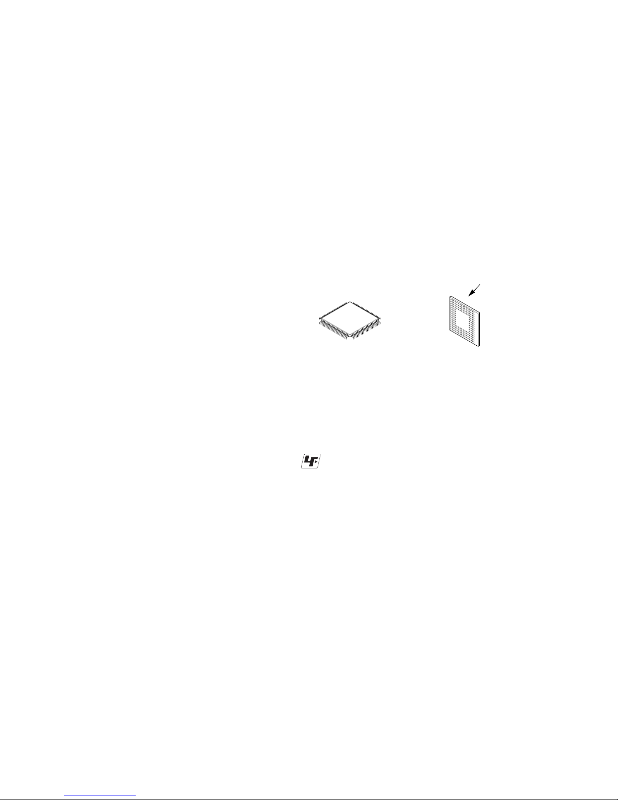
Notes on chip component replacement
•Never reuse a disconnected chip component.
• Notice that the minus side of a tantalum capacitor may be damaged by heat.
* Replacement of IC6201, IC7102 used in this set requires a special
tool.
• The voltage and waveform of CSP (chip size package) cannot be
measured, because its lead layout is different from that of conventional IC.
• Lead layouts
Unleaded solder
Boards requiring use of unleaded solder are printed with the leadfree mark (LF) indicating the solder contains no lead.
(Caution: Some printed circuit boards may not come printed with
the lead free mark due to their particular size.)
: LEAD FREE MARK
Unleaded solder has the following characteristics.
• Unleaded solder melts at a temperature about 40°C higher than
ordinary solder.
Ordinary soldering irons can be used but the iron tip has to be
applied to the solder joint for a slightly longer time.
Soldering irons using a temperature regulator should be set to
about 350°C.
Caution: The printed pattern (copper foil) may peel away if the
heated tip is applied for too long, so be careful!
• Strong viscosity
Unleaded solder is more viscous (sticky, less prone to flow) than
ordinary solder so use caution not to let solder bridges occur such
as on IC pins, etc.
• Usable with ordinary solder
It is best to use only unleaded solder but unleaded solder may
also be added to ordinary solder.
surface
Lead layout of
conventional IC
CSP (chip size package)
1. GENERAL ·········································································· 3
2. DISASSEMBLY
2-1. Cover (jack) ·································································· 4
2-2. Case··············································································· 5
2-3. Ornamental Belt, SW Board ········································· 5
2-4. AUDIO Board ······························································· 6
2-5. Cover (Chassis), Microphone Unit (MIC3201) ············6
2-6. MAIN Board, Liquid crysal,
Display Panel (LCD3201) ············································ 7
3. TEST MODE ······································································ 8
4. DIAGRAMS ······································································ 10
4-1. Block Diagrams
– Main Section-1 –······················································ 11
– Main Section-2 –······················································ 12
– Panel/Key Section – ················································· 13
4-2. Printed Wiring Board – AUDIO Board – ···················· 14
4-3. Schematic Diagram – AUDIO Board (1/2) –·············· 15
4-4. Schematic Diagram – AUDIO Board (2/2) –·············· 16
4-5. Printed Wiring Board – MAIN Board – ····················· 17
4-6. Schematic Diagram – MAIN Board (1/3) – ··············· 18
4-7. Schematic Diagram – MAIN Board (2/3) – ··············· 19
4-8. Schematic Diagram – MAIN Board (3/3) – ··············· 20
4-9. Printed Wiring Board – SW Board – ·························· 21
4-10. Schematic Diagram – SW Board – ····························· 22
4-11. IC Block Diagrams ····················································· 23
4-12. IC Pin Function Descriptions ······································ 25
5. EXPLODED VIEWS
5-1. Case Section································································ 31
5-2. Chassis Section ··························································· 32
6. ELECTRICAL PARTS LIST ······································· 33
3
ICD-S7
SECTION 1
GENERAL
This section is extracted from
instruction manual.
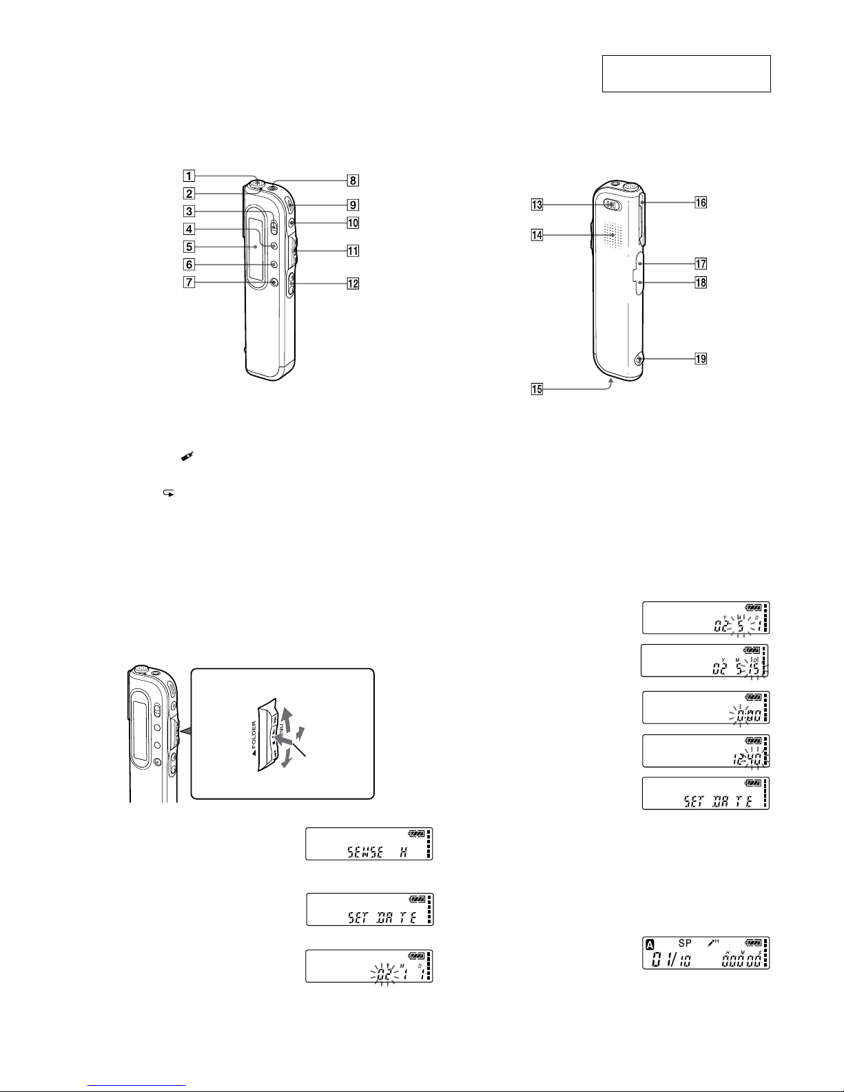
Step 2: Setting the Clock
You need to set the clock to use the alarm function or record the date and
time.
Clock setting display appears when you insert batteries for the first time,
or when you insert batteries after the unit has been without batteries for a
certain period of time. In this case, proceed from step 4.
1
Turn the jog lever toward
MENU.
The menu mode will be displayed in
the display window.
2
Press the jog lever up or down
(>/.) to select “SET DATE”.
3
Press the jog lever (x•B).
The date and time setting window is
displayed. The year digits will flash.
4
Set the date.
1 Press the jog lever up or down
(>/.) to select the digits of
the year.
Jog lever
Press the
center (x•B).
Press up (>).
Press down (.).
Turn
toward
MENU.
2 Press the jog lever (x•B).
The month digits will flash.
3 Set the month and day in
sequence, then press the jog lever
(x•B).
The hour digits will flash.
5
Set the time.
1 Press the jog lever up or down
(>/.) to select the digits of
the hour.
2 Press the jog lever (x•B).
The minute digits will flash.
3 Set the minute.
4 Press the jog lever (x•B).
The menu mode will be
displayed again.
Note
If you do not press the jog lever
(x•B) for more than one minute,
the clock setting mode is cancelled
and the window will return to
normal display.
6
Turn the jog lever toward
MENU.
The window will return to normal
display.
1 If the unit is left unused for more than 3 seconds in the stop mode after the
clock is set, the display will show the current time (page 25).
v
1 Built-in microphone (11)
2 OPR (operation) indicator
(11, 18)
3 DPC ON/OFF switch (28)
4 INDEX/
(bookmark)
button (30, 37)
5 Display window (22)
6 A-B
(repeat)/ (priority)
button (31, 42)
7 ERASE button (34)
8 EAR/MIC (earphone/
microphone) jack (13, 15)
Index to Parts and Controls
9 zREC (record) /REC
PAUSE button (11, 32)
0 xSTOP button (12, 19)
qa Jog lever
FOLDER/MENU/
.(review/fast backward)/
> (cue/fast forward)/
x• B (play/stop•enter)
qs VOL (volume) +/– buttons
(18)
Refer to the pages indicated in parentheses for details.
Front Rear
qd HOLD switch (27, 49)
qf Speaker
qg Battery compartment (6)
qh Clip*
qj USB connector (55)
qk DC IN 3V jack (6)
ql Slit for the supplied
handstrap
*Notes
•To prevent the clip from breaking,
avoid hooking it on thick fabric,
such as a pocket of a heavy coat.
•When bending down or running
with the unit clipped on your
pocket, be careful not to drop the
unit.
Index to Parts and Controls (continued)
4
ICD-S7
SECTION 2
DISASSEMBLY
Note : Follow the disassembly procedure in the numerical order given.
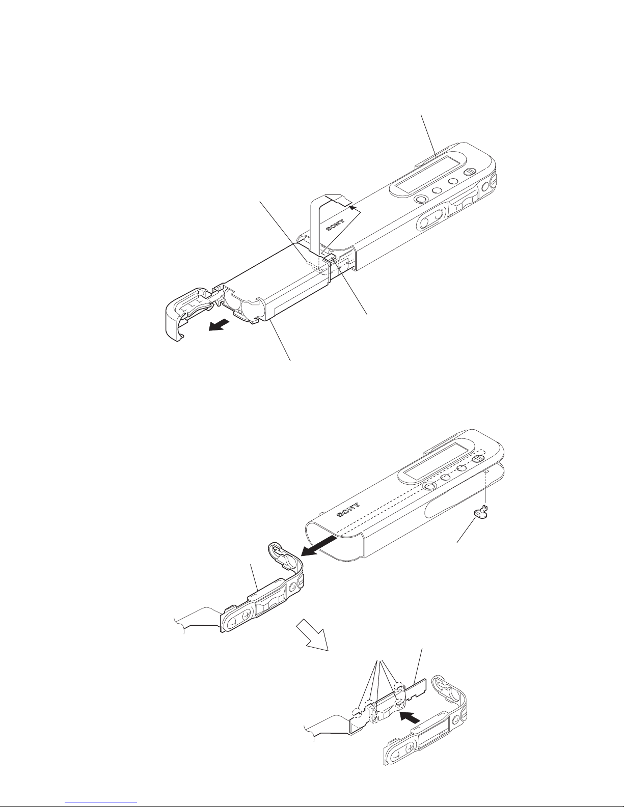
2-1. Cover (jack)
Note : Disassemble the unit in the order as shown below.
COVER(JACK)
(Page 4)
AUDIO BOARD
(Page 6)
ORNAMENTAL BELT, SW BOARD
(Page 5)
CASE
(Page 5)
COVER (CHASSIS),
MICROPHONE UNIT(MIC3201)
(Page 6)
MAIN BOARD,
LIQUID CRYSTAL
DISPLAY PANEL (LCD3201)
(Page 7)
SET
4
Screw (M 1.7 × 3)
6
Screw
(M 1.7
×
3)
2
Screw (M 1.4)
1
Battery lid
3
Lid (connector)
5
Cover (jack)
5
ICD-S7
2-2. Case
1
Sliding the chassis up to
the position of Connector.
3
Remove the chassis by sliding.
2
Connector
(CN7104)
Note : When assembling the chassis,
insert flexible board
.
2-3. Ornamental Belt, SW Board
2
Remove the ornamental belt
in the direction of the arrow.
Claws
3
SW board
(Cautions five claws)
1
Remove the knob (HOLD) .
6
ICD-S7
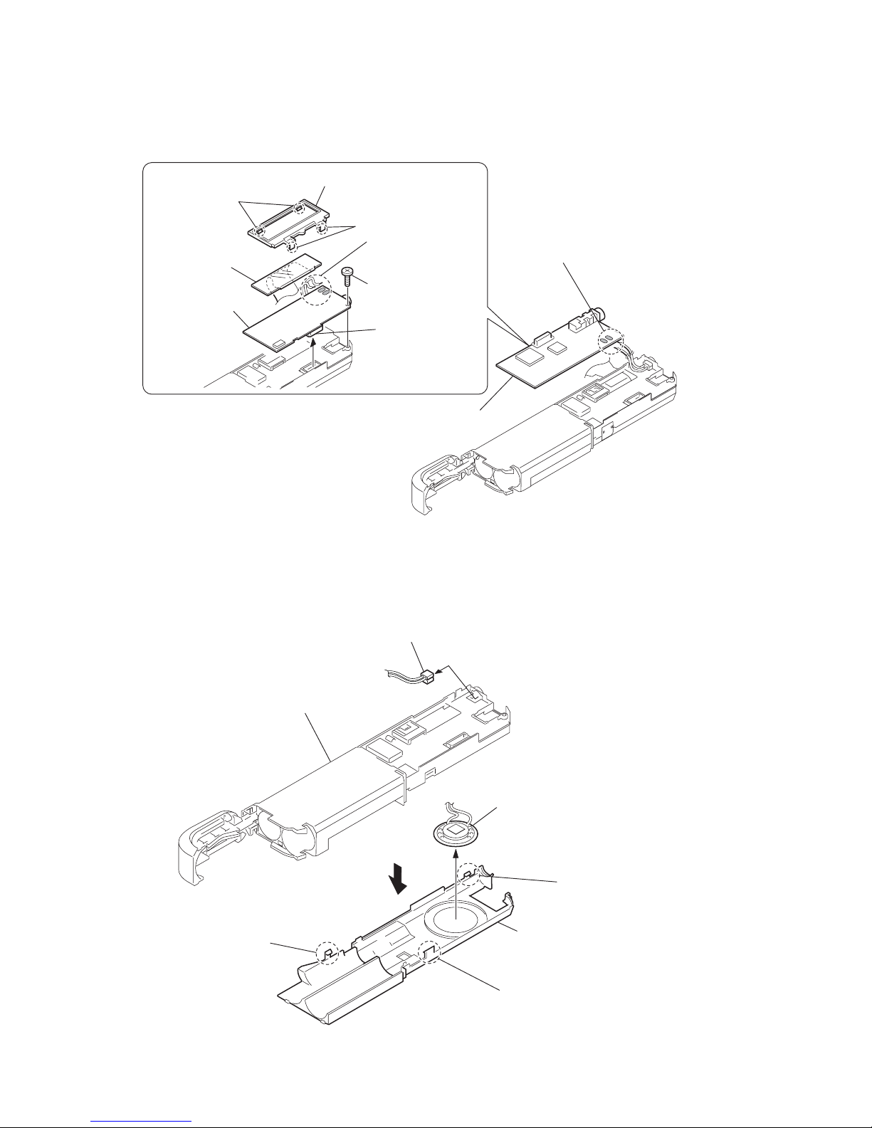
2-4. AUDIO Board
2
Speaker (1.5cm) (SP3201)
Claw
Chassis
Claw
Claw
1
Cover (chassis)
(Cautions three claws
)
3
Microphone unit (MIC3201)
2-5. Cover (Chassis), Microphone Unit (MIC3201)
7
AUDIO board
AUDIO board
4
Holder (LCD)
Two claws
Two claws
6
Turn over the AUDIO board
and
remove soldering (two points)
from Microphone cable.
3
Remove soldering
(two points)
from speaker cable.
2
Connector
(CAN7201)
5
Liquid crystal
display panel
(LCD3201)
1
Screw (M1.7 )
7
ICD-S7
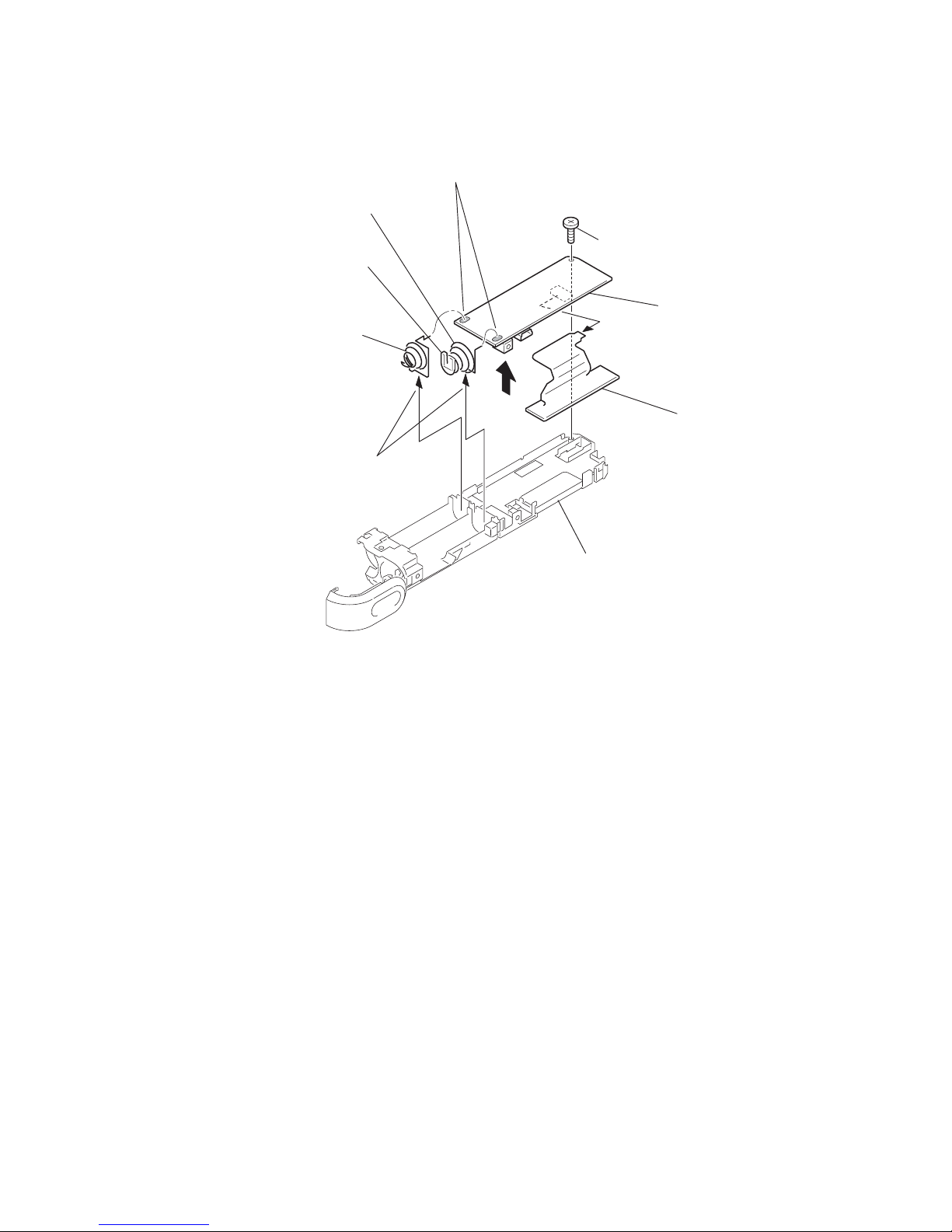
2-6. MAIN Board, Liquid Crystal, Display Panel (LCD3201)
8
MAIN board
3
Chassis
6
Terminal (-), battery
5
Terminal (+), battery
Cap (terminal)
4
Remove soldering (two points).
2
Remove the slot of a chassis.
7
Liquid crystal display panel
(LCD3201)
1
Screw (M1.7)
8
ICD-S7
SECTION 3
TEST MODE
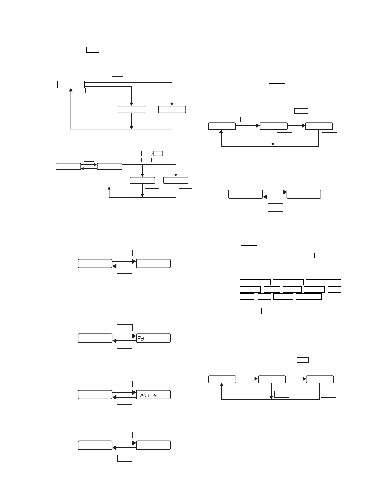
[Setting Method of the Test Mode]
There are two different methods to enter the test mode:
(1)To enter the test mode, turn on the HOLD switch while pressing
the STOP key and VOLUME+ key at the same time with the
power on.
(2) While pressing the VOLUME- key, turn on the power in state
that the test land (TP7101 (side B) or SL7101 (side A)) on the
main board is shorted to GND.
[Exiting Method of the Test Mode]
Exit the test mode by turning off the power.
[Initial Status of the Test Mode]
When the test mode is set, the LCD display appears as shown below.
LCD display
102 3C 01 J
Destination information
LPEC version
DSP version
CPU version
102 3C 01 J
LCD TEST
. >
SET AREA
. >
AUDIO TEST
. >
SLEEP TEST
. >
BEEP TEST
. >
SIO TEST
. >
KEY TEST
.
>
.
>
RESET MENU
> .
READ DATA
> .
DC JACK
> .
USB TEST
> .
LED TEST
> .
BATT TEST
> .
Initial status of test mode
Version display
Destination setting information display
END
TEST MODE
START
TEST MODE
[Operation in the Test Mode]
After entering the test mode, you can move within the test menu by
pressing the . / > key. You can move to the submenu by
pressing the x•B key. Then each test mode can be executed.
1. LCD test
• LCD is tested of all light-on and all light-off.
• Use the . / > key to adjust the contrast of the LCD. The
setting value is written in the EEPROM with the x•B key. If the
LCD test ends with OK, “**** OK ****” is displayed. If the
LCD test ends with NG, “****NG****” is displayed.
The default value is “0x12”.
x•B
LCD TEST
LCD ALL
LCD OFF
LCD CHECK
LCD ALL
LCD CHECK
:
:
STOP
STOP STOPSTOP
(select), (set)
.
>
x•B
LCD OFF
2. Setting destination
• NO destination information.
3. Audio test
Perform the through-playback and sine wave output.
• Contents of the submenu
ADA SP: AD/DA-through-SP mode
ADA LP: AD/DA-through-LP mode
DSP SP: DSP-through-SP mode
DSP LP: DSP-through-LP mode
1 kHz SIN: 1 kHz sine wave output mode
• Select the microphone sensitivity with the HOLD switch.
ON: High sensitivity OFF: Low sensitivity
•The VOR detection operation can be checked by the LED.
Sound: The red LED is turned on. No sound: The red LED is
turned off.
• MUTE can be set to “ON” or “OFF” with the ERASE key.
•The sound volume can be adjusted with the VOLUME+ key or
VOLUME- key during the audio test except the MUTE mode.
•The microphone sensitivity, sound volume and MUTE (on/off)
are displayed on the bottom of the LCD.
x•B
SET AREA
JAPAN USB
STOP
x•B
:
:
DSP SP
ADA LP
ADA SP
1K SIN
DSP LP
AUDIO TEST DSP LP
DSP LP H 10 DSP SP H 10 ADA LP H 10
(select), (set)
.
>
x•B
STOP STOP STOP
STOP
[Flow Chart of the Test Mode]
9
ICD-S7
4. Sleep test
•Pressing the x•B key causes the set to enter the sleep state.
•When the HOLD switch is ON, the LCD is turned off. When
OFF, the LCD is turned on.
•Press any keys to exit the sleep state.
5. Beep test
• Beep sound of 1.3 kHz or 2 kHz is output.
6. SIO test
•Perform the connection test of the RTC, EEPROM and serial to
parallel conversion IC.
• As to the test result, if all of the connection test are OK,
“****OK****” is displayed. If the connection test of the RTC is
NG, “**RTCNG**” is displayed. If the EEPROM is NG,
“**EEPNG**” is displayed.
7. Key entry test
•When the any key is pressed, the entry key and the A/D converted
value (hexadecimal) of the two channel keys are displayed.
•When the STOP key is pressed, the A/D value of the key is
displayed while the key is depressed. When the key is released,
the screen returns to the test menu.
8. Battery remaining power test
•The detected A/D value (hexadecimal) of the battery remaining
power is displayed.
9. LED/EL test
• LED (red and green) and EL are all turned on.
any keys any keys
SLEEP TEST
SLEEP IN
LCD OFF
(with HOLD OFF status)
x•B
(with HOLD ON status)
x•B
x•B
BEEP TEST
1.3K BEEP
2.0K BEEP
1.3K BEEP
1.3K BEEP
2.0K BEEP
:
:
(set)
x•B
(select),
.
>
STOP
STOP STOP
x•B
SIO TEST
SIO OK
STOP
x•B
KEY TEST
0-FF 1-FF
STOP
x•B
BATT TEST
STOP
10. USB test
• When the menu starts the USB self-check, either presence or
absence of the Vbus is judged.
(Vbus is present: “VBUS: ON”, Vbus is absent: “VBUS: OFF”)
•The USB driver always works regardless of presence or absence
of the USB signal only when Vbus is available during the USB
test. At this time, turning on HOLD causes the set to move to the
suspend state. Turning off the Vbus causes the set to return to the
test menu.
11. DC-IN test
LCD : Detection result of external DC power supply is display is
displayed of LCD.
12. DATA READ test (not used)
Not use for test command design check or verification.
13. Rest menu
•Pressing the x• B key causes the set to enter the menu
initialization standby state.
•When the following keys are all entered and the x•B key is
pressed, the initialization is executed. At the same time, the
Wak eUp signal is checked, too.
Check keys: VOLUME+ , VOLUME– , A-B REPEAT ,
INDEX , STOP , zREC , ERASE , . ,
x•B , > , MENU , FOLDER
and check states of Memory Stick insert and
outsert ( EJECT ).
• If all tests end in success, “**ALLOK**” is displayed. If the key
entry is NG or if any of the keys is not pressed yet, “**KEYNG**”
appears. If saving in the EEPROM is NG, “**MENUNG**”
appears.
x•B
LED TEST
LED EL ON
STOP
x•B
RESET RESET KEY
RESET OK
x•B
In the case that the key entry
and saving in the EEPROM end correctly,
after the check key is entered.
STOP
STOP
x•B
Suspend
USB VBUS ON
LCD OFF
When Vbus is on, HOLD key turns on.
STOP
or cut Vbus
STOP
cut Vbus
x•B
DC JACK JACK ON OFF
( )
STOP
10
ICD-S7
SECTION 4
DIAGRAMS
Note on Schematic Diagrams:
• All capacitors are in µF unless otherwise noted. pF: µµF
50 WV or less are not indicated except for electrolytics
and tantalums.
• All resistors are in Ω and 1/
4
W or less unless otherwise
specified.
•
f
: internal component.
• C : panel designation.
• A : B+ Line.
•Power voltage is dc 3V and fed with regulated dc power
supply from battery terminal.
•Voltages and waveforms are dc with respect to ground
under no-signal (detuned) conditions.
no mark : REC
[]: PB
∗
: Impossible to measure
•Voltages are taken with a VOM (Input impedance 10 MΩ).
Voltage variations may be noted due to normal production tolerances.
•Waveforms are taken with a oscilloscope.
Voltage variations may be noted due to normal production tolerances.
• Circled numbers refer to waveforms.
• Signal path.
F : PB
L : REC
* Replacement of IC6201, IC7102 used in this set requires
a special tool.
• The voltage and waveform of CSP (chip size package)
cannot be measured, because its lead layout is different
from that of conventional IC.
Note on Printed Wiring Boards:
• Y : parts extracted from the conductor side.
• b : Pattern from the side which enables seeing.
Caution:
Pattern face side: Parts on the pattern face side seen from
(SIDE B) the pattern face are indicated.
Par ts face side: Parts on the parts face side seen from
(SIDE A) the parts face are indicated.
* Replacement of IC6201, IC7102 used in this set requires
a special tool.
• Lead layouts
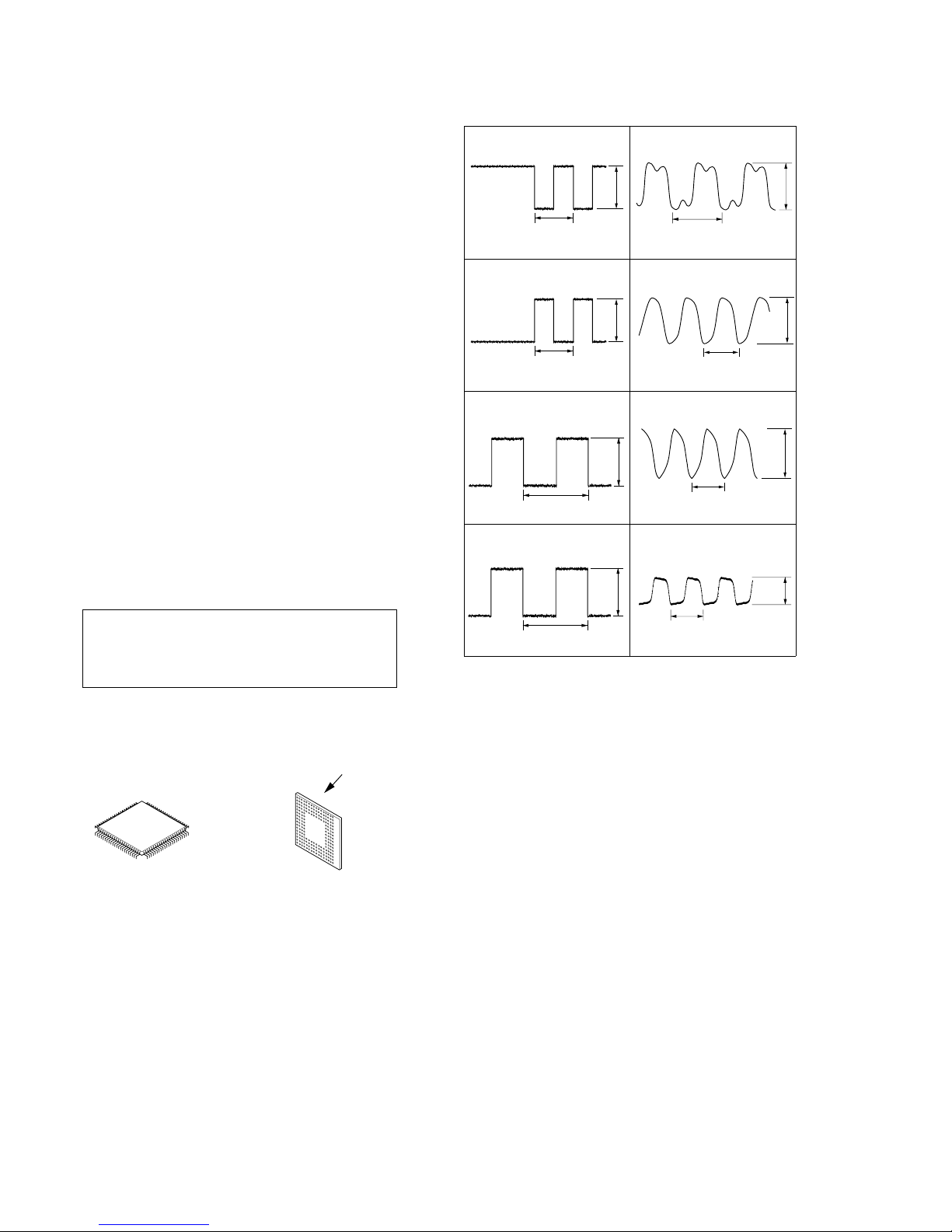
• WAVEFORMS
surface
Lead layout of
conventional IC
CSP (chip size package)
1 IC7101 wd (SCK1)
2 IC7101 wl (SIPCLK)
3 IC7101 es
(DSPSYSCK)
5 IC7101 ej (MSCLK)
6 IC7101 yd (CF2)
8 IC8101 qd (X OUT)
(USB Connection)
2 V/DIV, 4 µs/DIV
2 V/DIV, 40 ns/DIV
2 V/DIV, 4 µs/DIV
2 V/DIV, 200 ns/DIV
1 V/DIV, 40 ns/DIV
5.7 µs
567 ns
3.0 Vp-p
4 Vp-p
70 ns
3.1 Vp-p
3.9 Vp-p
71 ns
2 V/DIV, 20 ns/DIV
2 V/DIV, 40 ns/DIV
3.7 Vp-p
8.33 ns
5.1 µs
3.1 Vp-p
4.0 Vp-p
50 ns
4 IC7101 ef (FSCLK)
2 V/DIV, 10 µs/DIV
31 µs
3.0 Vp-p
7
IC7113 wd (XO)
1111
ICD-S7
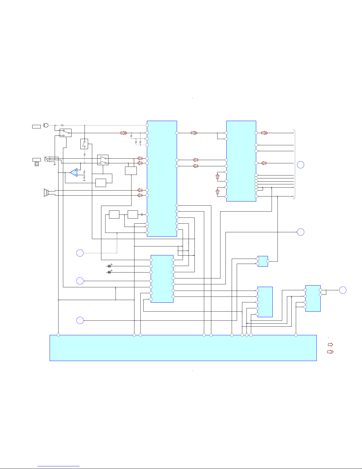
4-1. Block Diagrams – Main Section-1 –
Signal path
: REC
: PB
33239124343029
92 2
34
28
27
42
40
4
2
32
22
14
25
17
13
15
33
6
44
5
11
39
40
30
31
25
26
28
27
1
2
48
47
11
10
9
43
45
46
13
MIC3201
13
7
11
2
3
12
8
5
6
10
9
4
14
IC7107
SI/PO DRIVER
DATA
CLOCK
XLMUTE
SPPWR
HPPWR
HPMUTE
XREDLED
XGREENLED
XDSPRST
XEEPCS
15
XUSBRST
EEPRST
MICSEL
MICSEL
XBATTEN
XBATTEN
MICSENSE
D7102
RED(REC)
GREEN(PB)
6
3
1
IC6202
CLOCK GEN
IC7101 (1/3)
CPU
CLKIN
CE
Q0
Q1201,2201
MUTE
Q3201
SWITCH
Q3202
SWITCH
Q3206
SWITCH
J3201
(SPEAKER)
2
3
4
1
6
4
5
6
7
3
8
IC7106
EEPROM
IC7108
REAL TIME CLOCK
SK
DI
DO
CS
RESET
CLK
DATA
CE0
CE1
/AIRQ
/TIRQ
IC3201
MIC AMP, AGC,
HP AMP, POWER AMP
MICIN
35
MICVCC
LGAININ
BIASOUT
ROUT
LOUT
SPOUT+
SPOUT-
AGCDET
AGCSW
STBYSW
GAINSW
RECOUT
RIN
LIN
BEEPIN
MICPWR
HPPWR
SPPWR
MUTE
IC3202
ADC, DAC
RIN1
LIN1
ROUT2
LOUT2
OPGAR
ROUT1
OPGAL
LOUT1
STDO
STDO
BCLK
LRCK
SDTI
CDTI
CDTO
CCLK
XCS
XRST
XPD
MCK0
BCLK
LRCK
SO
ADACDTO
ADACDTI
ADACCLK
XADACS
XRST
MCLK
XUSBRST
HPJACK
AUPWR
AUPWR
SIPCLK
BEEP
5
MICPWR
FSCLK
RTCCS
SDO1
SDI1
SCK1
SP3201
B
A
C
F
D
E
WAKEUP
(OPR)
MIC
MIC
1
3
4
HPPWR
Q3207
Q1202,2202
Q3203,3208,
3209
DSPIVDD
IC3204
1212
ICD-S7
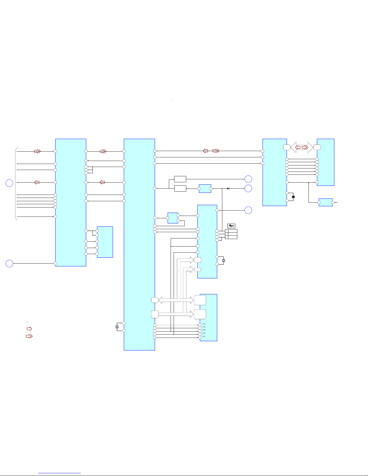
– Main Section-2 –
Signal path
: REC
: PB
68-75,
77-84
23-34,
37-40
43-49,
51-58,
26,27
12,17,18,23,
29,35,36,42,
7,13,14,20,
26,32,31,37
3-5,9,10,
15,16,22,
44-47,39,40,
33,34,28
16
42
17
41
1
8
XWE
XLB LB
WE
UB
XUB
7
31
60
20
6
USBDET
DREQ
XUSBCS
XUSBIRQ
D0-D15
56-53,
42-39
29-32,
41-44
MD0-MD7
I/O1-I/O16
A0-A16
A0-A16
A0-A16
15
3
11
2
XSRCS
XOE
XOE
OE
CS
IC7102
S-RAM
IC6203
FLASH MEMORY
45
35
47
40
8
7
6
5
138
46
48
52
159
150
49
160
157
50
55
158
11
12
5
2
6
3
1
14
13
12
35
32
8
38
37
39
62
63
13
MICSENSE
MICSENSE
2
5
1
IC7112
D-FF
D
CK
Q
8
9
17
CE
RE
ALE
CLE
R/B
I/O1-I/O8
16
7
1921
18
WE
WPXRST
XWE
XRE
XCE0
ALE
CLE
XBSY
IC7103
FLASH MEMORY
IC7113
MEMORY CONTROL
IC6201
DSP
ADASI
BCLK
LRCLK
SO
ADACDTO
ADACDTI
ADACCLK
XADACS
XRST
MCLK
TSO
TSCK
TSOEN
TSIEN
TSIOEN
TSI
REQ
CLKIN
FMSDIO
FMSCK
XFMWP
XFMCS
SDI
SDO
SCK
XWP
XCS
SDI0
SCK0
XDSPSIOEN
SDO0
DSPIFREQ
DSPSYSCK
MSDIO
MSCLK
MSBS
SDIO
SCKI
SBS
CF1
CF2
X7101
14.112MHz
14
13
XIN
5
VBUS
3
D-
4
D+
6
TRON
XOUT
X8102
12MHz
24
23
XI
XO
X7102
20MHz
G
D
A
IC7101 (2/3)
CPU
IC5108
D8101
21
Q7103
SWITCH
Q7102
SWITCH
47
45
42
41
44
43
17-22
DREQ0
CS
46
RST
INT0
HWR
LWR
RD
D0 - D15
D0 - D15
D0 - D15
A1 - A6
A0 - A5
1
2
3
VBUS
DD+
IC8101
USB CONTROLLER
VOLTAGE
DETECT
CN8101
KEYGND
H
E
DDCOUT
XUSBRST
φ
STDO
BCLK
LRCK
SO
ADACDTO
ADACDTI
ADACCLK
XADACS
XRST
MCLK
6
9
3
37
52
51
47
49
50
21
IC7114
RESET
MSVDD
 Loading...