Sony ICDR-100 Service manual
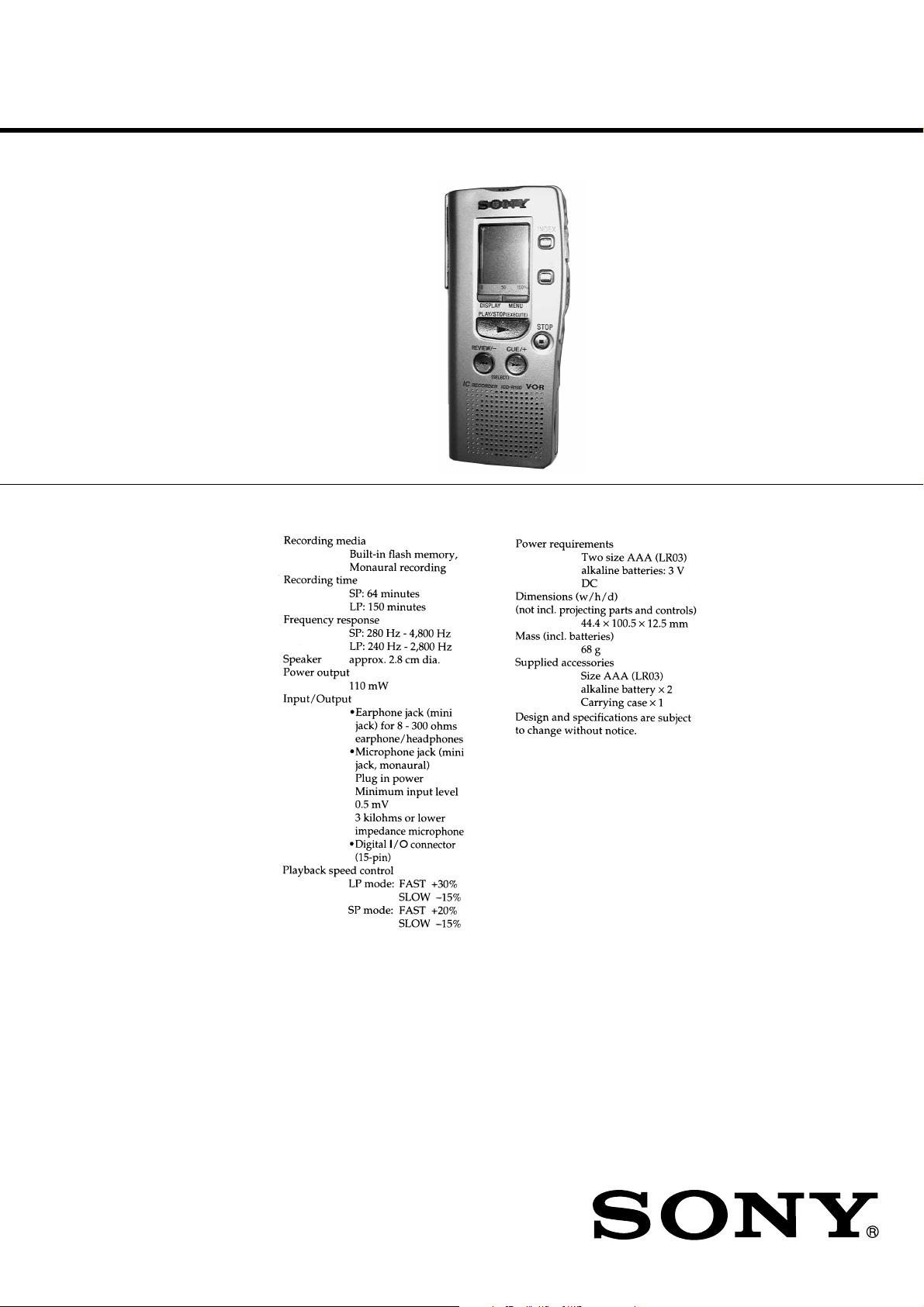
ICD-R100
SERVICE MANUAL
Ver 1.3 2001.03
SPECIFICATIONS
US Model
AEP Model
Tourist Model
9-926-975-13
2001C0200-1
© 2001.3
IC RECORDER
Sony Corporation
Audio Entertainment Group
General Engineering Dept.
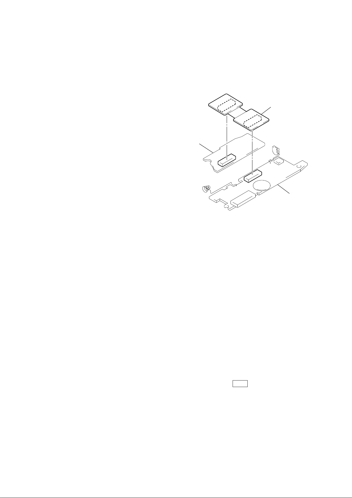
TABLE OF CONTENTS
d
Specifications ........................................................................... 1
1. SERVICING NOTE....................................................... 2
2. GENERAL ....................................................................... 3
SECTION 1
SERVICING NOTE
Using the special connector jig (J-2503-101-A) to connect the main
board and digital board will prove convenient when servicing the
unit with power applied.
3. DISASSEMBLY
3-1. Lid ASSY, Upper ........................................................ 5
3-2. Digital Board .............................................................. 5
3-3. Unit, Switch ................................................................ 6
3-4. Jack Board .................................................................. 6
3-5. Main Board ................................................................. 6
4. DIAGRAMS
4-1. Explanation of IC Terminals....................................... 7
4-2. Block Diagrams .......................................................... 9
4-3. Printed Wiring Boards (Main Section) ......................11
4-4. Schematic Diagram (Main Section) ......................... 13
4-5. Printed Wiring Boards (Digital Section) .................. 17
4-6. Schematic Diagram (Digital Section)....................... 18
5. EXPLODED VIEWS
5-1. Case Section ............................................................. 23
5-2. Main Board Section .................................................. 24
6. ELECTRICAL PARTS LIST.................................... 25
Flexible Circuit Board Repairing
• Keep the temperature of the soldering iron around 270°C during
repairing.
• Do not touch the soldering iron on the same conductor of the
circuit board (within 3 times).
• Be careful not to apply force on the conductor when soldering or
unsoldering.
Notes on chip component replacement
• Never reuse a disconnected chip component.
• Notice that the minus side of a tantalum capacitor may be damaged by heat.
Jig (J-2503-010-A)
Digital board
Main boar
Note : Do not apply excessive amounts of flux during replace-
ment of electronic components since this may cause electrical shorts due to moisture.
Wipe off flux after electronic components exchange.
CAUTION ON REPLACING FLASH MEMORY
The BAD-BLOCK check* must be executed, when the flash
memory (IC701) in this set was replaced.
The set will not operation normally, unless this check is finished.
* The BAD-BLOCK check detects an area (bad-block) in the flash
memory where data validity cannot be guaranteed, and saves
this information in the TOC-AREA so that a bad-block is not
used.
BAD-BLOCK check procedure :
1. Apply 3V from regulated power supply to the battery
terminals.
2. Once the power is supplied, the check starts and then
proceeds for approx. 3 minutes. (Be sure to keep applying
the power during the check)
3. When the check completes, the result is shown as bellows.
OK: Only the LCD back light LED (D503, 504) turns on.
NG: Red LED blinks or turns on or green LED turns on in
the OPR LED (D502),
4. In case of OK, press the STOP button.
Note :
• In case of NG, check system control IC (IC704), flash memory
IC (IC701) and the peripheral circuit. (Particularly, check carefully the soldering of the flash memory)
• After finishing the BAD-BLOCK check, assemble the set, load
the dry battery, and confirm if the set operates normally.
– 2 –
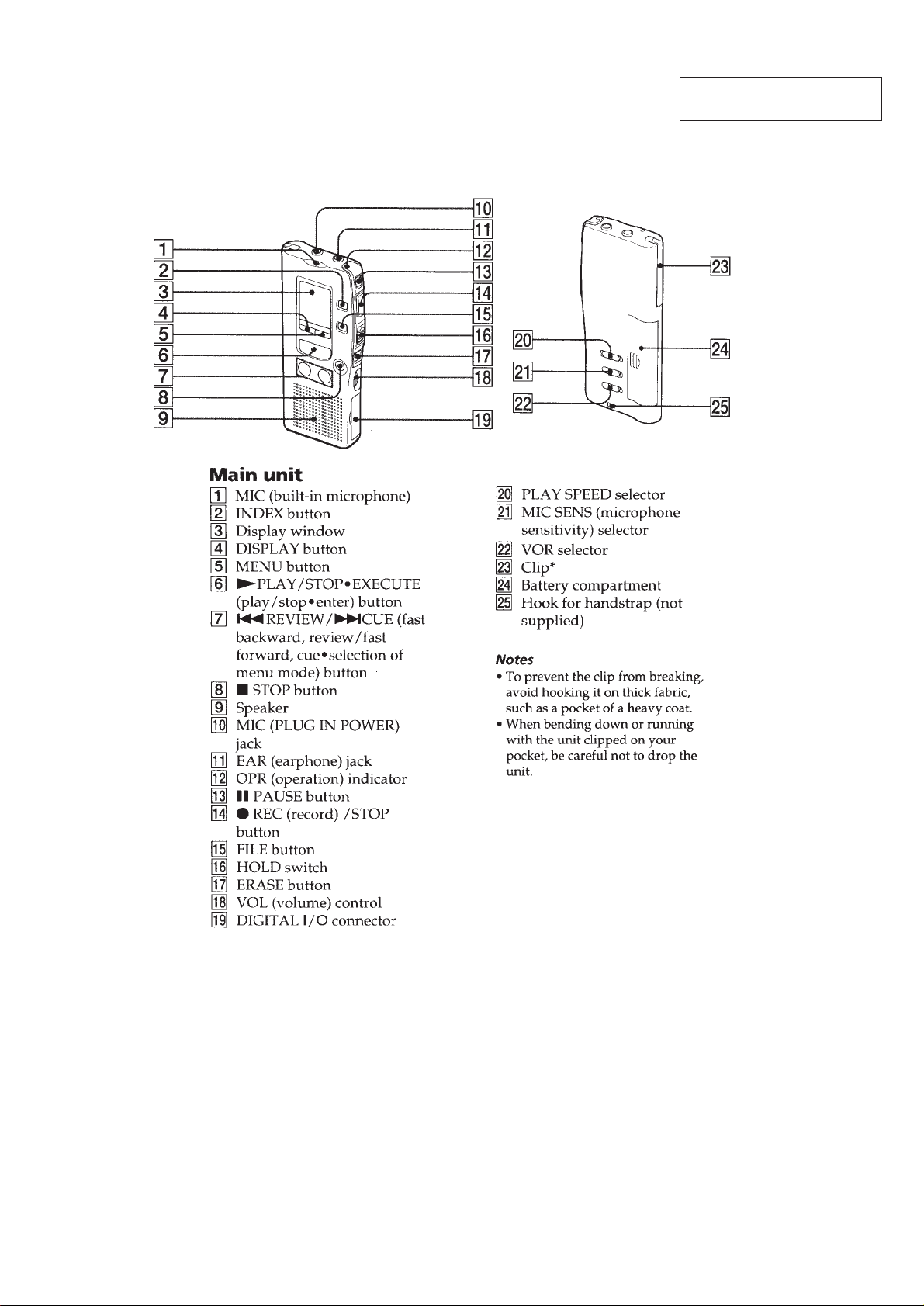
LOCATION AND FUNCTION OF CONTROLS
SECTION 2
GENERAL
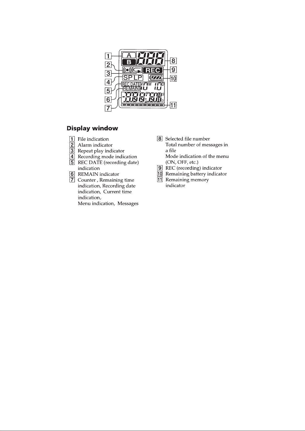
This section is extracted from
instruction manual.
– 3 –
– 4 –
SECTION 3
)
DISASSEMBLY
r
The equipment can be removed using the following procedure.
Set
Note : Follow the disassembly procedure in the numerical order given.
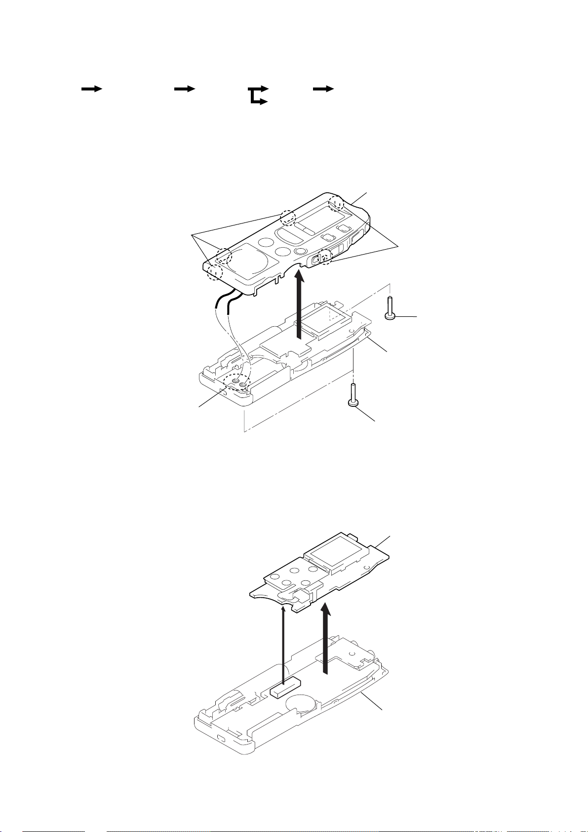
3-1. LID ASSY, UPPER
Lid ASSY, Upper
3
Digital board Jack board Main board
Unit, Switch
Claws
4
Lid ASSY, Upper
3
Claws
1
Screw (B1.7X10
5
Remover solder
3-2. DIGITAL BOARD
2
Case ASSY
2
Screws (B1.7X9)
Note : Not using a screw (10mm) of step
1 for this place.
Digital board
Remove the
1
connector
(CN703)
– 5 –
Case ASSY

d
Y
d
3-3. UNIT, SWITCH
e
3-4. JACK BOARD
Digital board
1
1
Screw (B1.7X4)
Unit, Switch
2
Double-sided adhesive tap
Note : The switch unit is secured with double-sided
adhesive tape.
When removed the switch unit, change it for
a new component.
3-5. MAIN BOARD
2
Remove the
connector
(CN102)
4
3
Jack boar
Case ASSY
Cap (Terminal)
Main boar
2
Claw
3
Claw
1
Case ASS
Cap (PC)
– 6 –
SECTION 4
DIAGRAMS
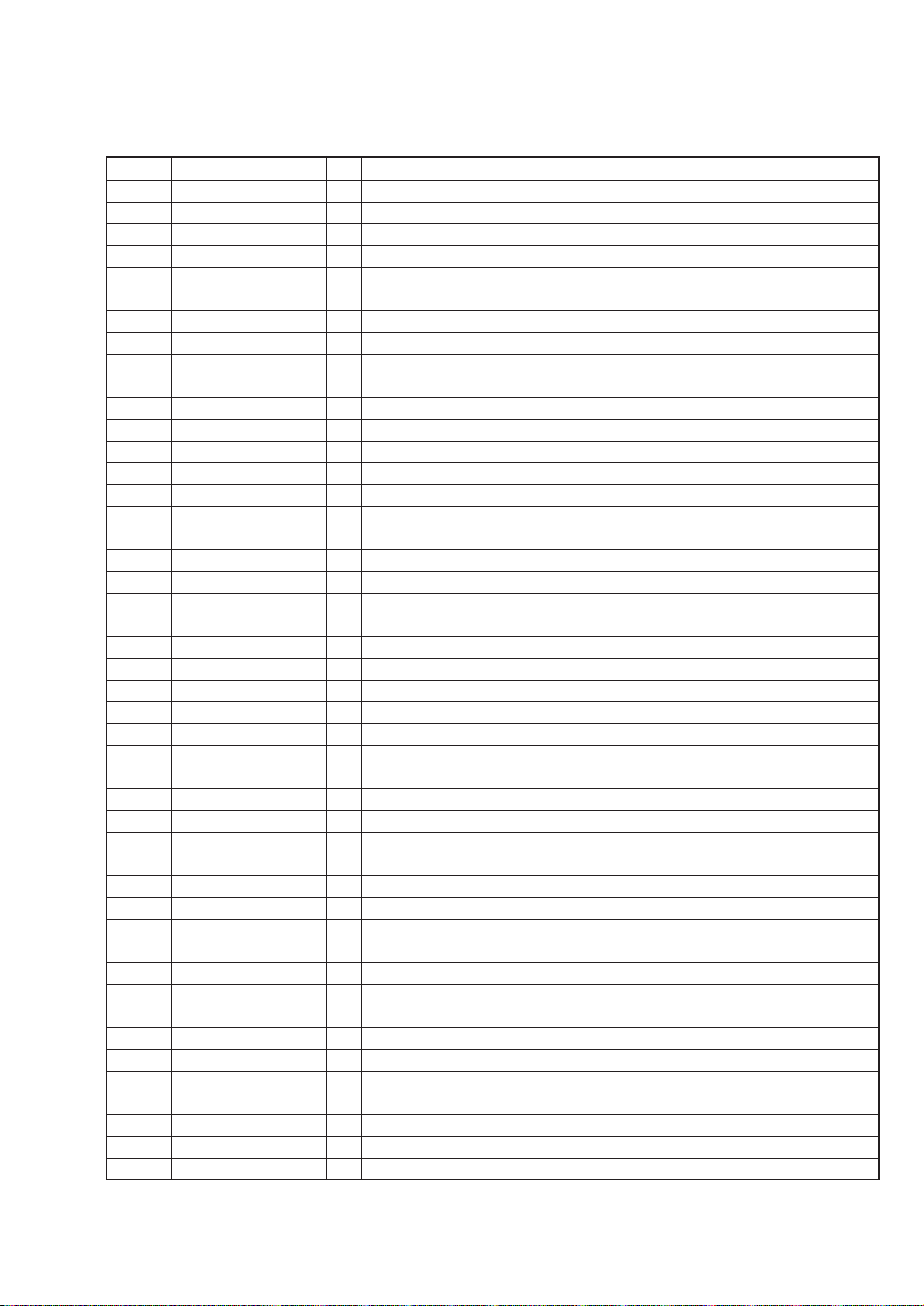
4-1. EXPLANATION OF IC TERMINALS
IC704 µPD780308GC-113-8EU (SYSTEM CONTROL)
Pin No. Pin name I/O Description
1 KEY0 I Key input
2 KEY1 I Key input
3 SPDSW I Playback speed switch input.
4 XHOLD I Hold switch input.
5 HPMUTE O Earphone mute output.
6 PCLE O PC link permission signal output.
7 XFMCE O CE output for flash memory.
8 VDDO – Power supply terminal.
9 AVREF I A/D reference voltage input.
10 XFMWE O Write enable signal output for flash memory.
11 XFMALE O ALE signal output.
12 VSS1 – Ground.
13 XFMR/B I Flash memory Ready/Busy signal input.
14 XFMCLE O CLE signal output for flash memory.
15 SYNCOUT O SYNC signal output.
16 SYNCMSK O SYNC output control signal output.
17 XFMRE O Flash memory read enable signal output.
18 MSKCLK I SYNC output control clock input.
19 XFMWP O Flash memory WP signal output.
20 XFMSE O Flash memory SE signal output.
21 BEEP O BEEP signal output (2.4kHz).
22 LIGHT O LCD back lignt control output.
23 – 26 COMO 0–3 O LCD common signal output.
27 BIAS – Connect to VCC (LCD BIAS).
28 – 30 VLC 0 – 2 – LCD drive power supply.
31 VSS0 – Ground.
32 – 61 S0 – S29 O LCD segment signal output.
62 XVORSW I VOR switch input.
63 XVORIN I VOR signal input.
64 XTEST I Test terminal.
65 XDSPDEN O DSP registor control I/F enable signal output.
66 LEDREC O REC LED (red) ON/OFF output.
67 LEDPB O PLAY LED (green) ON/OFF output.
68 AMPPOW O Power down control output for IC108.
69 SPOWER O IC101 and analog power supply control output.
70 RTCCE O Real time colck CE signal output.
71 XPDRST O Reset signal output for IC101.
72 DSPIS I Serial data input from IC101.
73 DSPIR O Playback serial data output for IC101.
74 XBLCK O DSP bit clock signal output.
75 RTCDI I Real time colck data input.
76 RTCDO O RTC data and DSP registor contrl data output.
77 RTCCLK O RTC I/F data and DSP registor control clock output.
78 IC – Ground.
79 X2 O System clock output (5MHz).
80 X1 I System clock input (5MHz).
– 7 –
 Loading...