

Sony ICDP-28 Service manual
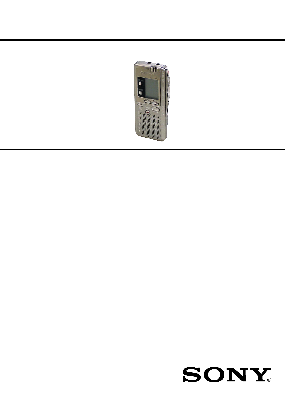
ICD-P28
SERVICE MANUAL
Ver 1.0 2004.03
SPECIFICATIONS
Recording media Built-in flash memory, Monaural recording
Recording time SP: 9 hours 40 minutes
LP: 15 hours 45 minutes
Frequency response 180 Hz - 3,500 Hz
Speaker approx. 3.2 cm (1 5/16 in.) dia.
Power output 250 mW
Input/Output • Earphone jack (minijack) for 8 - 300 ohms
ear receiver/headphones
• Microphone jack (minijack, monaural)
Plug in power
Minimum input level 0.6 mV
3 kilohms or lower impedance microphone
Power requirements Tw o LR03 (size AAA) alkaline batteries: 3 V DC
Dimensions (w/h/d) (not incl. projecting parts and controls)
44.5 × 105.3 × 14.0 mm (1 13/16 × 4 1/4 × 9/16 in.)
Mass (incl. batteries) 71 g (2.5 oz)
Supplied accessories LR03 (size AAA) alkaline batteries (2) (For the
US only)
USB connecting cable (1)
Application software (CD-ROM) (1)
US Model
Canadian Model
AEP Model
Tourist Model
Korean Model
9-877-649-01
2004C04-1
© 2004.03
Design and specifications are subject to change without notice.
IC RECORDER
Sony Corporation
Personal Audio Company
Published by Sony Engineering Corporation
1

ICD-P28
Notes on Chip Component Replacement
• Never reuse a disconnected chip component.
• Notice that the minus side of a tantalum capacitor may be dam-
aged by heat.
UNLEADED SOLDER
•
Boards requiring use of unleaded solder are printed with the leadfree mark (LF) indicating the solder contains no lead.
(Caution: Some printed circuit boards may not come printed with
the lead free mark due to their particular size.)
: LEAD FREE MARK
Unleaded solder has the following characteristics.
• Unleaded solder melts at a temperature about 40°C higher than
ordinary solder.
Ordinary soldering irons can be used but the iron tip has to be
applied to the solder joint for a slightly longer time.
Soldering irons using a temperature regulator should be set to
about 350°C.
Caution: The printed pattern (copper foil) may peel away if
the heated tip is applied for too long, so be careful!
• Strong viscosity
Unleaded solder is more viscous (sticky, less prone to flow)
than ordinary solder so use caution not to let solder bridges
occur such as on IC pins, etc.
• Usable with ordinary solder
It is best to use only unleaded solder but unleaded solder may
also be added to ordinary solder.
TABLE OF CONTENTS
1. SERVICE NOTE ................................................................ 3
2. GENERAL
Index to Parts and Controls ..................................................... 4
3. DISASSEMBLY
3-1. Case (Upper) Assy .............................................................. 5
3-2. F-SW Board, P-SW Board .................................................. 6
3-3. Main Board ......................................................................... 6
3-4. PC Board ............................................................................. 7
4. TEST MODE .......................................................................8
5. DIAGRAMS
5-1. IC Pin Description.............................................................11
5-2. Block Diagram .................................................................. 13
5-3. Printed Wiring Board – Main Section – ............................ 15
5-4. Printed Wiring Board – F-SW Section – ........................... 16
5-5. Printed Wiring Board – P-SW, PC Section – .................... 17
5-6. Schematic Diagram – Main Section (1/2) – ...................... 18
5-7. Schematic Diagram – Main Section (2/2) – ...................... 19
5-8. IC Block Diagrams............................................................20
6. EXPLODED VIEWS
6-1. Case Section ...................................................................... 21
6-2. Main Board Section .......................................................... 22
7. ELECTRICAL PARTS LIST ........................................23
2
SECTION 1
R105
SERVICE NOTE
1-1. CAUTIONS OF FLASH MEMORY (IC701)
EXCHANGE
[Precaution when the flash memory (IC701) is replaced]
When the flash memory (IC701) is replaced, be sure to perform the
BAD BLOCK check* and writing of the model code. If they are not
completed, the unit will not operate normally.
* BAD BLOCK check is to check the flash ROM memory
area (the BAD BLOCK area) where data cannot be
guaranteed. The resultant information of this check is stored
in the TOC-AREA so that the BAD BLOCK area should
not be used.
[BAD BLOCK Check Procedure]
1. When the power is turned on after the flash memory (IC701) is
replaced, the BAD BLOCK check starts automatically and the
OPR (D701) lights in orange.
2. In about 30 seconds after start of the check, the OPR (D701)
changes the color to green indicating that the check is
completed.
ICD-P28
MAIN BOARD (SIDE B)
R101
TP102
FB102
C125
R128
FB104
TP714 TP715
RED
(REC)
D701
D701
OPR
GRN
(PLAY)
B E B
C C
Q701
R717
R716
FB101
TP101
R102
TP719
FB103
TP718
R103
R110
C114
R104
C110
C102
C101
C106
C105
R133
C104
C112
C116
C111
X101
30
31
50
51
R135
C107
3
ICD-P28
SECTION 2
GENERAL
Index to Parts and Controls
Main unit
MIC jack
(PLUG IN POWER)
(built-in microphone)
MIC
EAR (earphone) jack
OPR (operation) indicator
This section is extracted
from instruction manual.
Rear
Display window
FOLDER
DIVIDE
DISPLAY
MIC SENS
(microphone sensitivity)
MENU
ERASE
Speaker
STOP
Battery
compartment
Display window
Remaining memory indicator
Folder indication
Alarm indicator
Microphone sensitivity indication
Repeat play indicator
zREC (record) /STOP
X PAUSE
– ./ >+ SELECT
(ENTER)
NxPLAY/STOP
(ENTER)
HOLD
VOL (volume)
USB connector
Remaining battery
indicator
Recording mode
indication
REC (recording)
indicator
Selected message
number/number of
messages in a folder
Hook for handstrap
(not supplied)
Counter /Remaining time indication /Recording date and
time indication /Current time indication (15:30, etc.) /Menu
indication (ALARM, BEEP, etc.) /Mode indication of the
menu (ON, OFF, etc.) /Messages (ERASE, HOLD, etc.)
4
SECTION 3
y
DISASSEMBLY
Note : This set can be disassemble according to the following sequence.
SET
3-1. CASE (UPPER) ASSY
(Page 5)
3-2. F-SW BOARD,
P-SW BOARD
(Page 6)
3-3. MAIN BOARD
(Page 6)
3-4. PC BOARD
(Page 7)
ICD-P28
Note : Follow the disassembly procedure in the numerical order given.
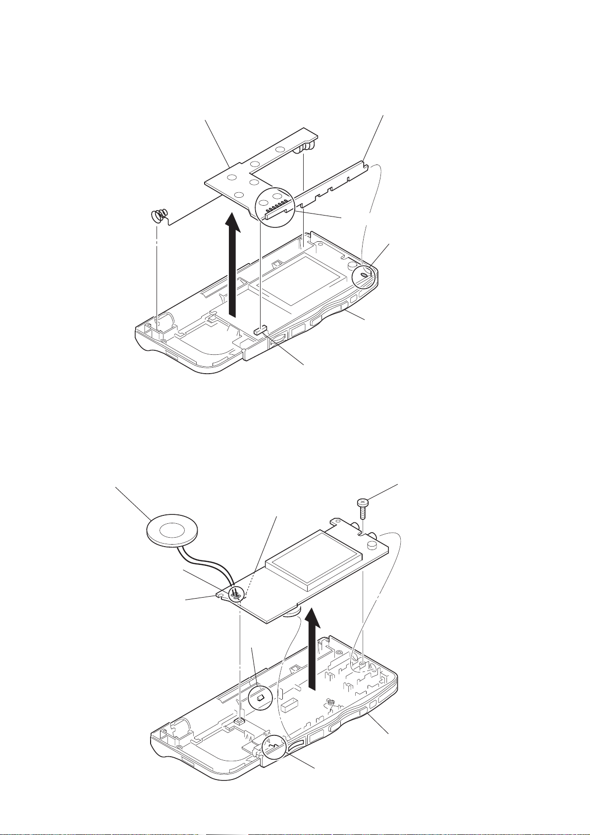
3-1. CASE (UPPER) ASSY
3
two claws
9
speaker (SP101)
6
claw
8
two
screws
x
(1.7
2.5)
7
0
case (upper) ass
5
three claws
case block assy
2
screw
(B 1.7x7)
4
claw
1
screw
(B 1.7x10)
5
ICD-P28
3-2. F-SW BOARD, P-SW BOARD
6
F-SW board
5
P-SW board
3-3. MAIN BOARD
2
speaker (SP101)
3
2
CN703
4
Removal the seven solders.
1
Removal the solder.
case block assy
3
screw
(1.7x4)
1
Removal the two solders.
8
MAIN board
4
claw
6
CN801
5
7
case (lower) assy
claw
6
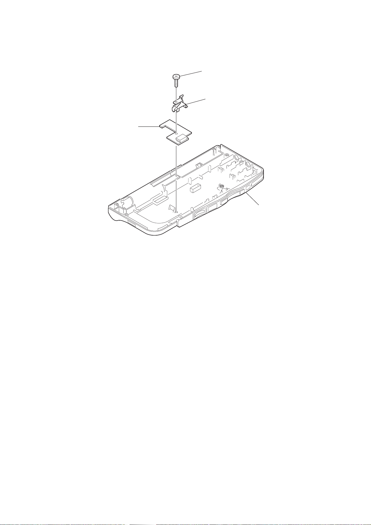
3-4. PC BOARD
y
2
PC board
1
screw
(1.7
x
3
holder (jack)
ICD-P28
3.7)
case (lower) ass
7
ICD-P28
SECTION 4
TEST MODE
[Setting Method of the Test Mode]
(1) To enter the test mode , turn on the HOLD switch while
pressing the STOP key and MENU key at the same time with
the power on.
[Exiting Method of the Test Mode]
Exit the test mode by turning off the power.
[Initial Status of the Test Mode]
When the test mode is set, the LCD display appears as shown
below.
LCD display
/091
P17
091tIC702 version
(Displayed to A or B folder
when version a or b.)
P17tSet code
[Flow Chart of the Test Mode]
START
TEST MODE
Initial status of
Test mode.
Set code,LPEC ST,
.>
F/W version display
LCD
.>
.>
RST
MENU
.>
[Operation in the Test Mode]
After entering the test mode, you can move within the test menu by
pressing the . / > key. You can move to the submenu by
pressing the x•B key. Then each test mode can be executed.
1. LCD test
• LCD is tested all light-on and all light-off.
x • B
LCD LCD
STOP
ALL
•
•
•
OFF LCD
CHK LCD
ALL LCD
•
•
•
. / >
x • B
LCD
ON
(SET)
LCD
OFF
(SELECT)
CHK
START
.
/ .
CHK
END
STOP STOP STOP
2. Audio test
Perform the through-playback.
• Contents of the submenu
DSPLOP: DSP through mode.
• Select the microphone sensitivity with the MIC SENS switch.
HtLtHtLt
……
• MUTE can be set to “ON” or “OFF” with the ERASE key.
•The sound volume can be adjusted with the VOL volume key
during the audio test except the MUTE mode.
•This test operates in accordance with to the JA CK detection test.
It displays the current mode, microphone sensitivity and mute
on the LCD display.
[Example of LCD display]
DSP through mode/MIC: H/MUTE: OFFtH/OF/DSPLOP
AUDIO
.>
SLEEP
.>
BEEP
.>
>
RTC
.
END
TEST MODE
COUNT
>
.
Turning off the power.
USB
LED
BATTKEY
KEY
.>
.>
.>
x • B
AUDIO DSPLOP
STOP
. / >
(SET)
x • B
H
OF
DSPLOP
(SELECT)
STOP
8

ICD-P28
3. Sleep test
•Pressing the x•B key causes the set to enter the sleep state.
•Press any keys to exit the sleep state.
x • B
with
off
HOLD
SLEEP SOON
SLEEP
any keys
4. Beep test
• Beep sound of 1.3 kHz or 2 kHz is output.
x • B
. / >
x • B
(SELECT)
(SET)
6. Key entry test
•When the any key is pressed, the entry key and the A/D
converted value (hexadecimal) of the two channel keys are
displayed.
KEY IN0 is displayed on the upper side and KEY IN1 on the
lower side.
•When the STOP key is pressed, the A/D value of the key is
displayed while the key is depressed. When the key is released,
the screen returns to the test menu.
x • B
OFF
KEY KEY,OFF
STOP
7. Battery remaining power test
•The detected A/D value (hexadecimal) of the battery remaining
power is displayed.
x • B
BATT BATT
STOP
u
AA
BEEP 1.3k
STOP
•
•
•
2.0k
1.3k
•
•
•
1.3k 2.0k
STOP
5. RTC test
•Perform the connection test of the RTC, EEPROM.
x • B
ON
RTC RTC
STOP
(1) RTC EEPROM test
This test checks that any data is written and read to and from
specific registers (verify check) and that data is cleared.
(2) RTC clock function test
This test checks that the time is updated at intervals of 1 second
in the micro processor by the RTC.
• It determines whether a test result is OK or NG.
If NG, it indicates that either device of R TC or EEPR OM was
found to be NG.
(All OKs: RTC OK/R TC NG: R TC B AD/EEPR OM NG: EEP
BAD)
ONON
STOP
8. LED test
• LED ( OPR : orange) are all turned on.
x • B
LED LED
STOP
ON
9
 Loading...