

Sony ICDBP-100, ICDBP-120 Service manual
ICD-BP100/BP120
SERVICE MANUAL
Ver 1.0 2001. 03
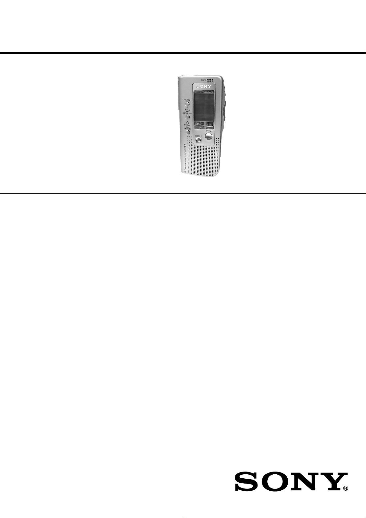
Photo : ICD-BP100
SPECIFICATIONS
Recording media Built-in flash memory, Monaural recording
Recording time ICD-BP100: SP: 63 minutes, LP: 168 minutes
Frequency response SP: 250 Hz - 7,300 Hz
Speaker approx. 3.2 cm (1
Power output 300 mW
Input/Output • Earphone jack (minijack) for 16 - 300 ohms
Playback speed control FAST +30%, SLOW –15%
Power requirements Two LR03 (size AAA) alkaline batteries: 3 V DC
Dimensions (w/h/d)
Mass (incl. batteries) 79 g (2.79 oz)
Supplied accessories Earphone × 1
Optional accessories Electret Condenser Microphone ECM-Z60, ECM-
ICD-BP120: SP: 127 minutes, LP: 339 minutes
LP: 300 Hz - 3,500 Hz
earphone/headphones
• Microphone jack (minijack, monaural)
Plug in power
Minimum input level 0.6 mV
3 kilohms or lower impedance microphone
• USB connector
(not incl. projecting parts and controls)
44.5 × 105.3 × 14.0 mm (1 13/16 × 41/4 × 9/
Carrying case × 1
LR03 (size AAA) alkaline battery × 2 (U.S.A. model
only)
Connecting cable × 1 (ICD-BP100 only)
“Digital Voice Editor” (CD-ROM) × 1
Registration card × 1 (U.S.A. and European models
only)
T115
Earphone MDR-ED228LP, MDR-E818LP
Connecting cord RK-G64
5
/
in.) dia.
16
US Model
ICD-BP100/BP120
Canadian Model
AEP Model
UK Model
E Model
ICD-BP100
Tourist Model
ICD-BP100/BP120
in.)
16
9-873-072-11
2001C1600-1
© 2001.3
Your dealer may not handle some of the above listed optional accessories. Please
ask the dealer for detailed information.
Design and specifications are subject to change without notice.
IC RECORDER
Sony Corporation
Audio Entertainment Group
General Engineering Dept.

ICD-BP100/BP120
TABLE OF CONTENTS
1. GENERAL ·································································· 3
2. DISASSEMBLY
2-1. Sub Block Assy, Upper Lid············································· 4
2-2. F-SW Board ····································································4
2-3. Main Board, P-SW Board ··············································· 5
2-4. PC Board········································································· 5
3. DIAGRAMS
3-1. Block Diagram ································································ 7
3-2. Printed Wiring Board – Main Section (1/2) –················· 8
3-3. Printed Wiring Board – Main Section (2/2) –················· 9
3-4. Schematic Diagram – Main Section (1/3) –·················· 10
3-5. Schematic Diagram – Main Section (2/3) –·················· 11
3-6. Schematic Diagram – Main Section (3/3) –·················· 12
3-7. Schematic Diagram – F-SW Section – ························· 13
3-8. Printed Wiring Board – F-SW Section (1/2) –·············· 14
3-9. Printed Wiring Board – F-SW Section (2/2) –·············· 15
3-10. Printed Wiring Board – PC Section – ························· 16
3-11. Schematic Diagram – PC Section – ···························· 17
3-12. Printed Wiring Board – P-SW Section – ···················· 18
3-13. Schematic Diagram – P-SW Section – ······················· 19
3-14. IC Block Diagrams ····················································· 20
3-15. IC Pin Function Description ······································· 21
4. EXPLODED VIEWS
4-1. Upper Lid Assy Section ················································ 23
4-2. Main Board Section ······················································ 24
Flexible Circuit Board Repairing
• Keep the temperature of the soldering iron around 270°C during
repairing.
• Do not touch the soldering iron on the same conductor of the
circuit board (within 3 times).
• Be careful not to apply force on the conductor when soldering or
unsoldering.
Notes on chip component replacement
• Never reuse a disconnected chip component.
• Notice that the minus side of a tantalum capacitor may be damaged by heat.
* Replacement of IC109 used in this set requires a special tool.
• The voltage and waveform of CSP (chip size package) cannot be
measured, because its lead layout is different from that of conventional IC.
• Lead layouts
surface
Lead layout of
conventional IC
CSP (chip size package)
5. ELECTRICAL PARTS LIST ·································· 25
Unleaded solder
Boards requiring use of unleaded solder are printed with the leadfree mark (LF) indicating the solder contains no lead.
(Caution: Some printed circuit boards may not come printed with
the lead free mark due to their particular size.)
: LEAD FREE MARK
Unleaded solder has the following characteristics.
• Unleaded solder melts at a temperature about 40°C higher than
ordinary solder.
Ordinary soldering irons can be used but the iron tip has to be
applied to the solder joint for a slightly longer time.
Soldering irons using a temperature regulator should be set to
about 350°C.
Caution: The printed pattern (copper foil) may peel away if the
heated tip is applied for too long, so be careful!
• Strong viscosity
Unleaded solder is more viscous (sticky, less prone to flow) than
ordinary solder so use caution not to let solder bridges occur such
as on IC pins, etc.
• Usable with ordinary solder
It is best to use only unleaded solder but unleaded solder may
also be added to ordinary solder.
2
SECTION 1
GENERAL
ICD-BP100/BP120
This section is extracted from
instruction manual.
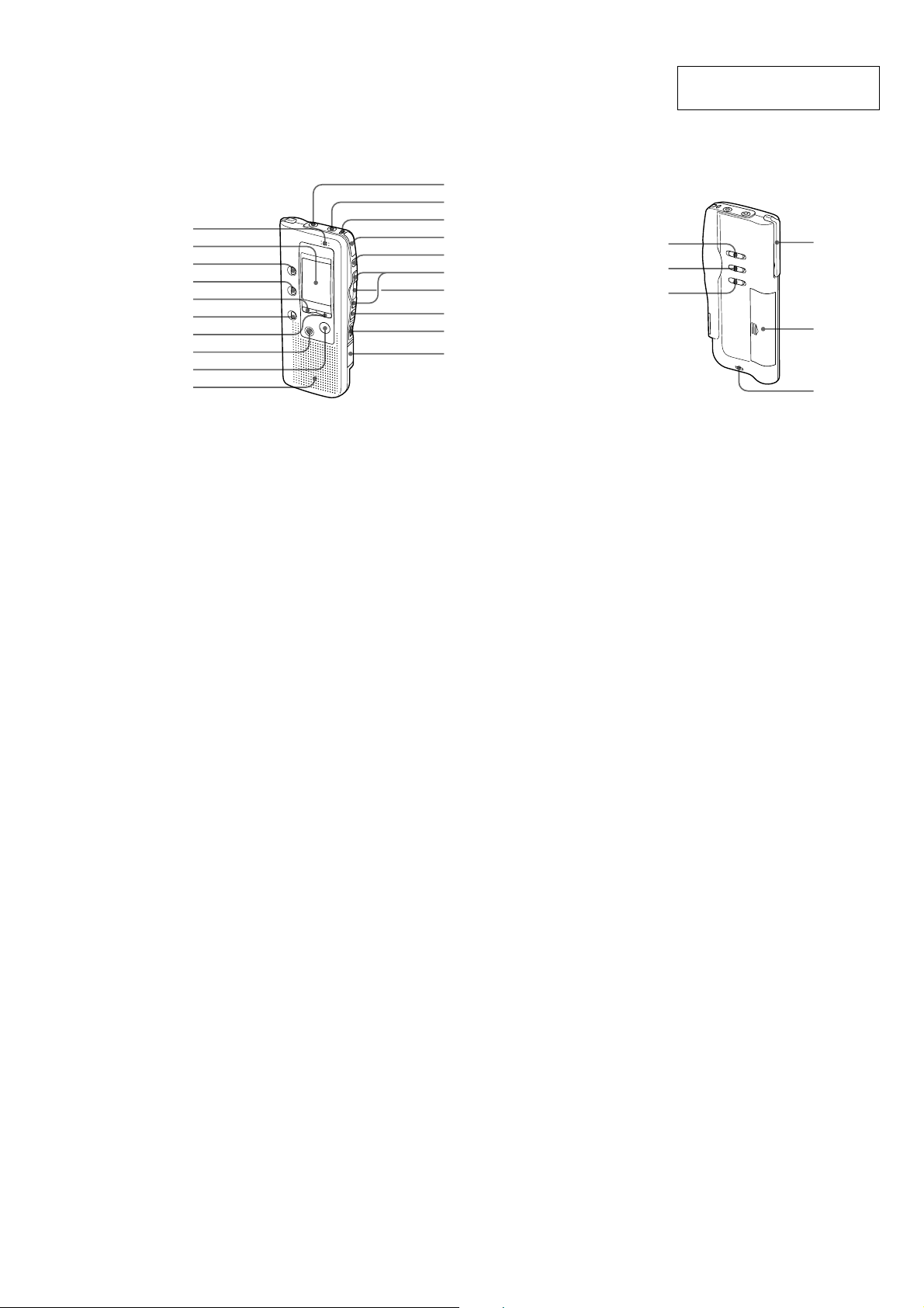
Main unit
1
2
3
4
5
6
7
8
9
q;
1 MIC (built-in microphone)
(12)
2 Display window (64)
3 FOLDER button (12, 16)
4 INDEX/BOOKMARK
button (22, 26)
5 DISPLAY button (39)
6 A-B REPEAT/PRIORITY
button (23, 30)
7 MENU button (10, 32, 35, 40,
41)
8 ERASE button (20)
9 xSTOP button (13, 17)
q; Speaker
qa MIC (PLUG IN POWER)
jack (15)
qs EAR (earphone) jack (14, 17)
qd OPR (operation) indicator
(12, 17)
qa
qs
qd
qf
qg
qh
qj
qk
ql
w;
qf zREC (record) /STOP
button (13, 24)
qg X PAUSE button (13, 17)
qh .REVIEW/>CUE (fast
backward, review/fast
forward, cue•selection of
menu mode) button (10, 16,
18, 19, 22, 26, 30, 32, 35, 40,
41)
qj NxPLAY/STOP
•EXECUTE (play/
stop•enter) button (10, 17,
18, 29, 30, 32, 35, 40, 41)
qk HOLD switch (38)
ql VOL (volume) control (17)
w; USB connector for
connecting to a computer
(48)
Rear
wa
ws
wd
wa PLAY SPEED selector (18)
ws MIC SENS (microphone
sensitivity) selector (14)
wd VOR selector (15)
wf Clip*
wg Battery compartment (8)
wh Hook for handstrap (not
supplied)
wf
wg
wh
3
ICD-BP100/BP120
d
y
d
r
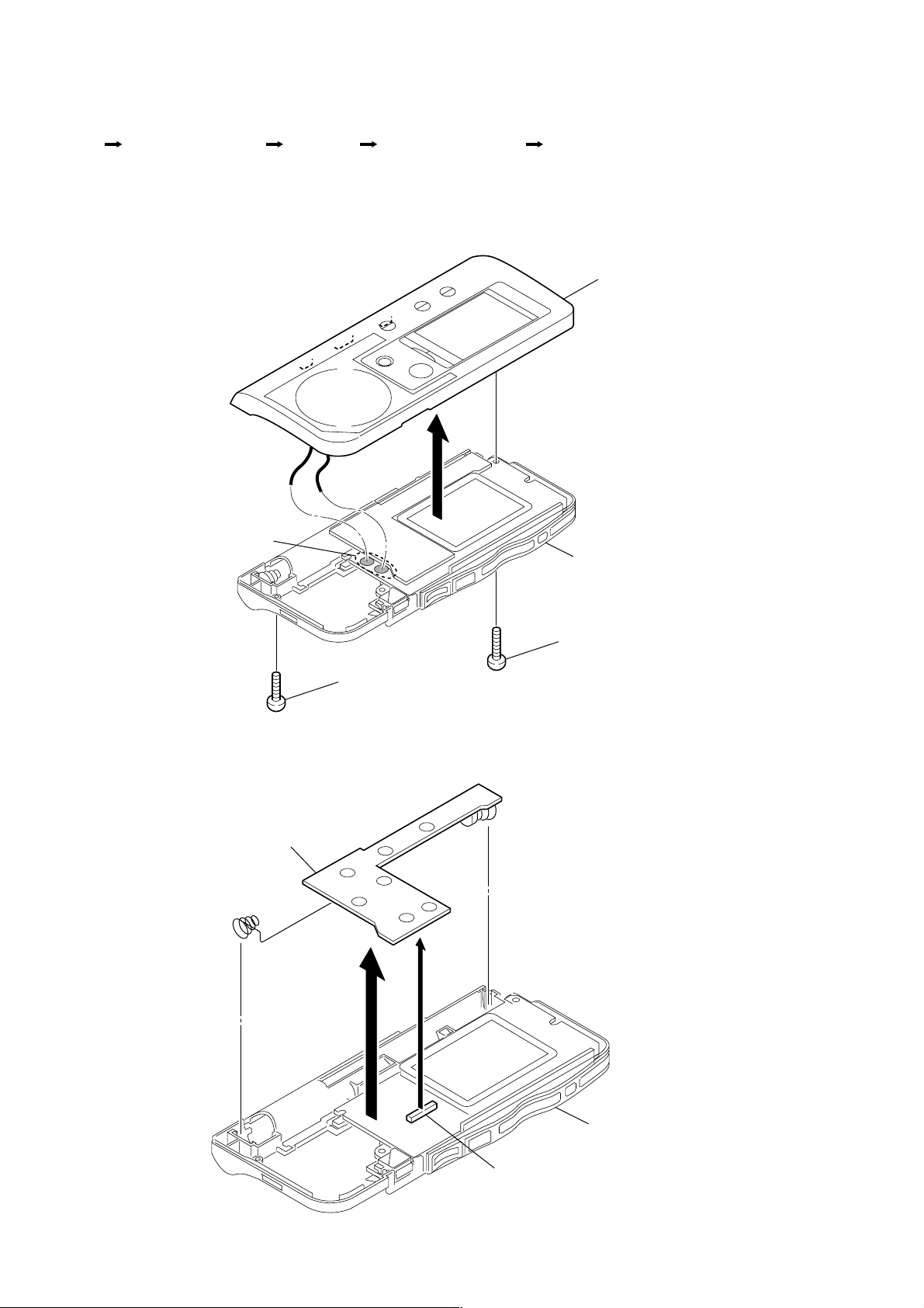
Disassemble the unit in the order as shown below.
SECTION 2
DISASSEMBLY
Sub block assy,upper lidSet
F-SW board MAIN board, P-SW board
Note : Follow the disassembly procedure in the numerical order given.
2-1. SUB BLOCK ASSY, UPPER LID
4
3
Remove the soldering
PC boar
case assy
sub block assy, upper li
5
2-2. F-SW BOARD
F-SW board
3
2
screw (B1.7 × 7)
2
1
screw (B1.7 × 10)
case ass
1
connector (CN703)
4
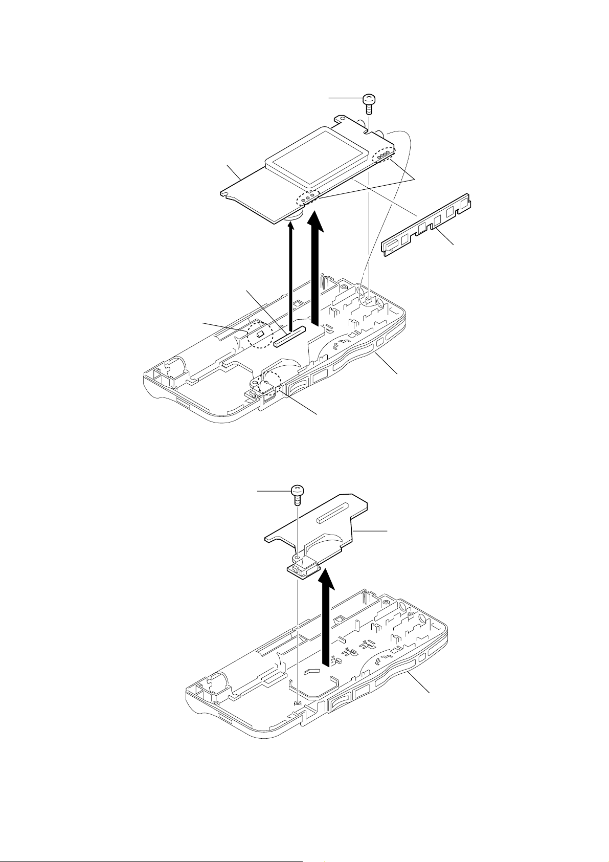
2-3. MAIN BOARD, P-SW BOARD
d
y
4
Main board
2
connector
(CN802)
1
screw (1.7
ICD-BP100/BP120
×
4)
5
Remove the soldering
6
P-SW boar
3
2-4. PC BOARD
claw
screw (1.7 × 4)
1
claw
2
case assy
3
PC board
case ass
5
ICD-BP100/BP120
SECTION 3
DIAGRAMS
Note on Schematic Diagrams:
• All capacitors are in µF unless otherwise noted. pF: µµF
50 WV or less are not indicated except for electrolytics
and tantalums.
• All resistors are in Ω and 1/
specified.
f
•
• C : panel designation.
• A : B+ Line.
• Power voltage is dc 3V and fed with regulated dc power
• Voltages and waveforms are dc with respect to ground
• Voltages are taken with a VOM (Input impedance 10 MΩ).
• Waveforms are taken with a oscilloscope.
• Circled numbers refer to waveforms.
• Signal path.
* Replacement of IC109 used in this set requires a special
• The voltage and waveform of CSP (chip size package)
: internal component.
supply from battery terminal.
under no-signal (detuned) conditions.
no mark : REC
( ) : PB
Voltage variations may be noted due to normal production tolerances.
Voltage variations may be noted due to normal production tolerances.
E : PB
a : REC
tool.
cannot be measured, because its lead layout is different
from that of conventional IC.
4
W or less unless otherwise
r
WAVEFORMS
1
IC712 od XTAL
4.096 MHz
VOLT/DIV : 0.5 V AC
TIME/DIV : 50 nsec
2
IC716 8 oscout
32.768 kHz
VOLT/DIV : 0.2 V AC
TIME/DIV : 10 µsec
3
IC508 5 EXT
3.3 µs
VOLT/DIV : 1.0 V DC
TIME/DIV : 2 µsec
1.3 Vp-p
0.8 Vp-p
3.2 Vp-p
Note on Printed Wiring Boards:
• Y : parts extracted from the conductor side.
• b : Pattern from the side which enables seeing.
Caution:
Pattern face side: Parts on the pattern face side seen from
(SIDE B) the pattern face are indicated.
Parts face side: Parts on the parts face side seen from
(SIDE A) the parts face are indicated.
* Replacement of IC109 used in this set requires a special
tool.
• Lead layouts
Lead layout of
conventional IC
CSP (chip size package)
surface
6
3-1. BLOCK DIAGRAM
ICD-BP100/BP120
MIC101
MIC
J101
MIC
(PLUG IN POWER)
CN801
USB
VBUS1
DD+
ID
GND
MAIN BOARD
PC BOARD
S101
MIC SENS
IC803, Q801
VOLTAGE
DETECTOR
1
2
3
4
5
S702
VOR
S701
PLAY
SPEED
SLOW NORMAL FAST
Q802
ON
OFF
F-SW BOARD(2/2)
Q101
MIC
SENSE
LH
SW
X801
24MHz
S705 - 701
S707 - 706
21
USBDET
69
USB_D-
USB_D+
68
67
XEXTCAPON
12
XIN
XOUT
13
IC101
MIC AMP
3
VIN+
VIN-
4
IC801
USB INTERFACE
FLMIO00
FLMIO15
XFLMRB
XFLMRE
XFLMCE0
FLMCLE
FLMALE
XFLMWE
XFLMWP
1 3 5
VOUT
SOT2
28
ZSI
SIN2
27
ZSO
SCK2
29
ZSCK
1
8
RST
54
ı
ı
39
55
58
64
62
61
59
56
18
ZIFREQ
20
ZIFACK
P-SW BOARD
IC802
RESET
IC102
ALC AMP
IN OUT
S721, S723 - 725
ZVCC
S722
VBUS1
Q702
+B
SW
IC103
VOR CONTROL
1
INPUT
29
ı
32
•
41
ı
44
12
•
37
6
OUT1
IC706
FLASH MEMORY
IO1
ı
IO8
VCC
Q705 - 706
WAKE UP
SW
S726
R/B
CLE
ALE
WE
WP
IC107
A/D, D/A CONVERTER
VIN VOUT
4
IC106
7
8
RE
9
CE
16
17
18
19
29
SCK1
27
SI1
31
SO1
28
SIEN1
33
SOEN1
42
P3
43
P2
SYSTEM CONTROL
DSPIFREQ
96
13
DCOMDT
12
XDIFEN
14
SIN1
15
SOT1
16
SCK1
57
XVORIN
99
VBUSOFF
10
XZRST
FLMIO00
103
ı
FLMIO15
118
97
ZIFREQ
40
ZIFACK
FLMRB
5
XFLMRE
3
XFLMCE0
101
FLMCLE
56
FLMALE
55
4
XFLMWE
120
XFLMWP
52
FLMSEL
50
XVORSW
49
SPEED
95
WAKEUP
KEYPUP
53
KEYIN0
47
KEYIN1
48
HOLDSW
100
ı
PDWN
DOUT
IC109
DSP
IC712
DSPSYSCK
ADASYSCK
22
20
17
XTI
8
BCK
9
FS
10
DIN
11
38
SI2
35
SO2
37
SIEN2
34
SOEN2
SCK2
CLKIN
/RESET
DSPPWR
XDSPRST
DSPACK
SOT2
SIN2
SCK2
SIPCS
RTCCE
RTCINTR
SUBCLK
BATT
BEEP
HPJACK
XHSTBY
XRESET
XTALIN
XTAL
COM0
COM3
SEG00
SEG31
ı
ı
IC105
36
59
72
IC104, IC108
CLOCK GEN
CLKIN
9 6
6
7 6
58
11
36 4
35
37
41
1
98
74
46
2
51
86
90 1
92
93
59
ı
62
17
ı
32
•
64
ı
72
•
75
ı
81
1
1
Q0
CE
CE
Q0
CLKIN
X701
4.096MHz
3
3
Q707
SW
LIQUID
CRYSTAL
DISPLAY
Q106
LPF
SW
IC112
AMP
VIN- VOUT
4 1
SI/PO DRIVER
MICSENSE
13
SOT2
DATA
2
3
CLOCK
XFLMPWR
15
AVCC
IC716
REAL-TIME CLOCK
SI
SO
3
SCLK
2
OSCIN
OSCOUT
7
CE
6
INTR
1
32KOUT
IC710
RESET
Q107, 108
LPF
SW
IC715
XSPPWR
XHPPWR
HPMUTE
XREDLED
XGRNLED
APOWER
ADAPWR
XLIGHT
XBATTEN
Q710
SW
32.768KHz
9
8
LMUTE
X702
7
11
12
8
5
6
10
9
4
14
VBUS1
RV101
wVOL
D702
Q102
MUTE
RED(REC)
GRN(PB)
IC110
POWER AMP
13
D703
OPR
F-SW BOARD(1/2)
AVCC
IC504, Q502
DSPVCC
MICVCC
ADAVCC
VBUS2
SVCC
ZVCC
CONVERTER
5 2
VOUT
5 2
VOUT
5 2
VOUT
D701,
D702
(BACK
LIGHT)
5 2
VOUT
DC-DC
IC505
+2.9V REG
CE
3
IC506
+2.9V REG
CE
3
IC501
+3.1V REG
CE
3
IC502
+3.3V REG
CE
3
17
IN1
+
-
6
INV
IN2
OUT
3 1
IC111
EARPHONE AMP
INA OUTA
2
STBY
1
Q104
SW
VIN
VIN
VIN
VIN
Q105
BUFFER
15
STNBY
Q103
SW
IC508, Q503
DC-DC
CONVERTER
(3.2V)
IC503, Q501
DC-DC
CONVERTER
(3.7V)
AVCC
RF
13
IC507, Q504
VOLTAGE
DETECTOR
11
8
Q110
MUTE
SP101
(SPEAKER)
J102
EAR
• Signal Path
: PB
: REC
DRY BATTERY
SIZE "AAA"
(IEC DESIGNATION LR03)
2PCS 3V
77
ICD-BP100/BP120
3-2. PRINTED WIRING BOARD – MAIN SECTION (1/2) –
12
A
B
C
J101
MIC
(PLUG IN POWER)
D
E
F
J102
G
EAR
MAIN BOARD (SIDE A)
3 4 5 6 7 8 9 10 11 12 13 14 15 16 17 18 19 20 21 22 23
IC 101
• : Uses unleaded solder.
IC 103
BP100
1
IC 102
24
* Replacement of IC109 used in this set requires a special tool.
TO
A
PC BOARD
(Page 16)
30 1
IC 104
IC 109
Q102
E C B
3160
IC 111
R766
R765
C160
C168
C161
C169
H
I
J
K
OPR
• Semiconductor Location
Ref. No. Location
D703 I-2
IC101 F-6
IC102 F-8
IC103 D-8
IC104 G-10
IC105 J-5
IC106 I-11
IC107 H-7
IC108 I-9
IC109 G-12
Ref. No. Location
IC110 G-16
IC111 D-21
IC112 I-11
Q101 E-8
Q102 B-20
Q103 B-18
Q104 B-19
Q105 B-16
Q106 H-11
Q107 E-21
Q108 F-21
Q110 F-21
IC 105
IC 107
12 13
IC 108
IC 112
CSP (Chip Size Package)
IC 106
IC 110
RV101
wVOL
1-680-349-
12
(12)
88
3-3. PRINTED WIRING BOARD – MAIN SECTION (2/2) – • : Uses unleaded solder.
ICD-BP100/BP120
12
A
MAIN BOARD
B
C
SP101
(SPEAKER)
D
E
F
G
3 4 5 6 7 8 9 10 11 12 13 14 15 16 17 18 19 20 21 22 23
IC 716
(SIDE B)
BP100
R772
B
F-SW BOARD
TO
(Page 15)
24
IC 706
115
CN702
1
TO LCD
C763
136
IC 715
60
61
31
30
IC 712
MIC101
MIC
H
I
J
• Semiconductor
Location
Ref. No. Location
D701 G-5
D702 I-7
IC706 F-13
IC710 H-15
IC712 E-18
IC715 C-21
IC716 F-3
30 16
C757
D
TO
P-SW BOARD
(Page 18)
25 48
C726
IC 710
C172
90
91 120
1
C
P-SW BOARD
(Page 18)
TO
1-680-349-
12
(12)
Q702 G-10
Q705 I-5
Q706 I-4
Q707 C-19
Q710 D-10
99
 Loading...