

Page 1
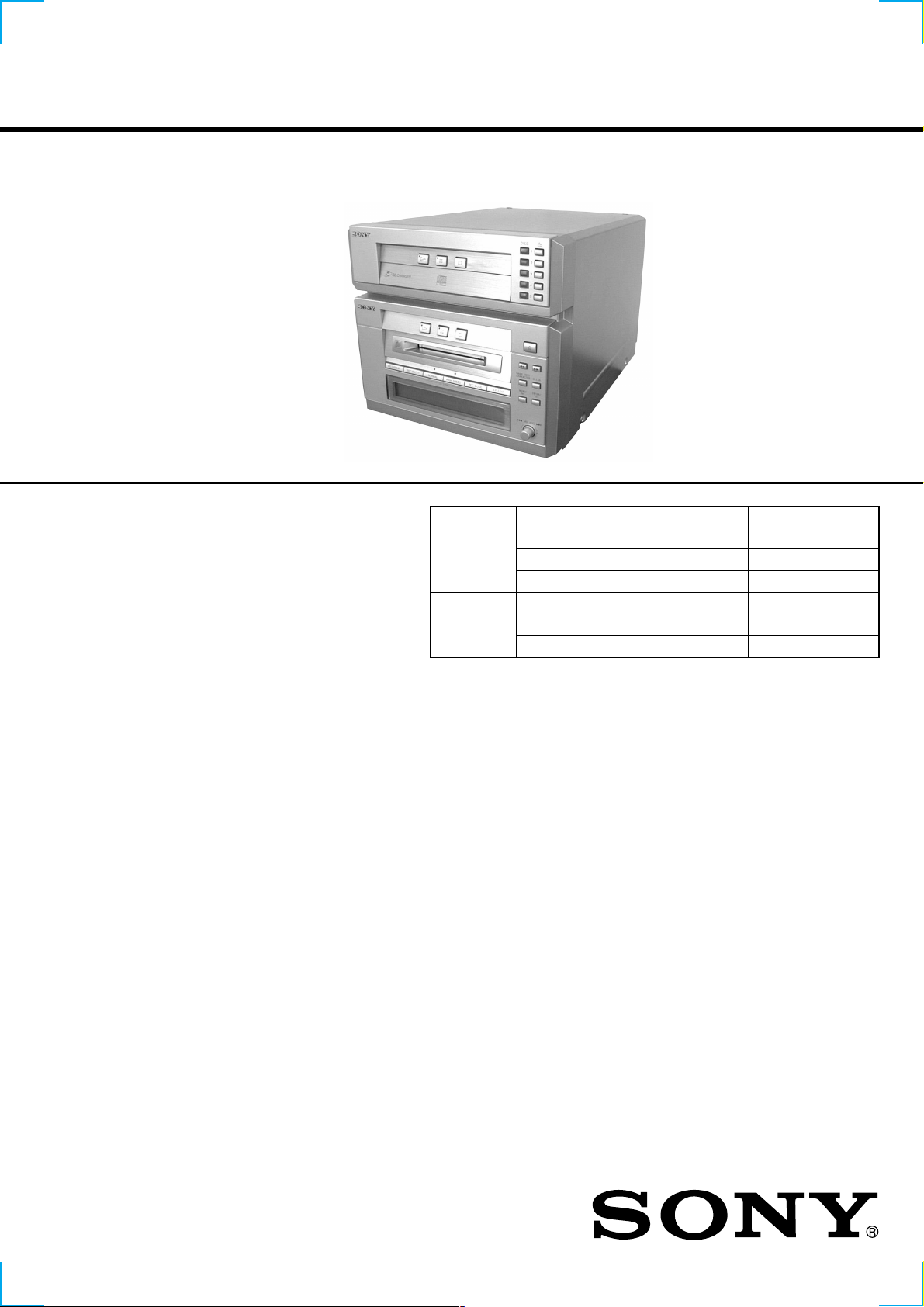
HMC-NX5MD
q
SERVICE MANUAL
HMC-NX5MD is the CD player and MD
Deck section in DHC-NX5MD
CD
Section
MD
Section
AEP Model
UK Model
E Model
Model Name Using Similar Mechanism NEW
CD Mechanism Type CDM53E-K4BD40
Base Unit Name Type BU-K4BD40
Optical Pick-up Name KSM-213DHAP/Z-NP
Model Name Using Similar Mechanism NEW
MD Mechanism Type MDM-7B
Optical Pick-up Name KMS-260B/J1N
CD player section
System Compact disc and digital audio
Laser Semiconductor laser
Laser output Max. 44.6 µW*
Wavelength 780 – 790 nm
Frequency response 20 Hz – 20 kHz (±0.5 dB)
Signal-to-noise ratio More than 90 dB
Dynamic range More than 90 dB
MD deck section
System MiniDisc digital audio system
Laser Semiconductor laser
Laser output Max. 44.6 µW*
Sampling frequency 44.1 kHz
Fre
uency response 20 Hz – 20 kHz
system
(λ=780 nm)
Emission duration: continuous
*This output is the value measured
at a distance of 200 mm from the
objective lens surface on the
Optical Pick-up Block with 7 mm
aperture.
(λ=780 nm)
Emission duration: continuous
*This output is the value measured
at a distance of 200 mm from the
objective lens surface on the
Optical Pick-up Block with 7 mm
aperture.
SPECIFICATIONS
General
Power requirements
European models: 230 V AC, 50/60 Hz
Other models: 120 V, 220 V or 230 – 240 V AC,
Power consumption
European models: 190 watts
Other models: 220 watts
Dimensions (w/h/d) Approx. 225 × 202 × 356 mm
Mass Approx. 4.3 kg
Supplied accessories: AM loop aerial (1)
Design and specifications are subject to change
without notice.
MINI Hi-Fi COMPONENT SYSTEM
50/60 Hz Adjustable with voltage
selector
Remote Commander (1)
Batteries (2)
FM lead aerial (1)
Speaker cords (2)
Front speaker pads (8)
1
Page 2
SELF-DIAGNOSIS FUNCTION
The self-diagnosis function consists of error codes for customers which are displayed automatically when errors occur, and error codes which
show the error history in the test mode during servicing. For details on how to view error codes for the customer, refer to the following box
in the instruction manual. For details on how to check error codes during servicing, refer to the following “Procedure for using the SelfDiagnosis Function (Error History Display Mode)”.
Self-diagnosis Display
This system has a Self-diagnosis display function
to let you know if there is a system malfunction.
The display shows a code made up of three or five
letters and a message alternately to show you the
problem. To solve the problem refer to the
following list. If any problem persists, consult
your nearest Sony dealer.
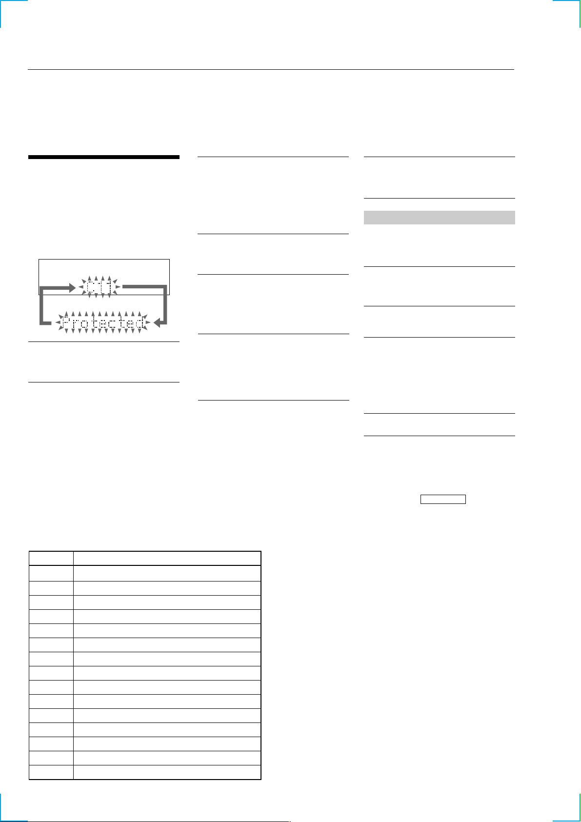
C11/Protected
The MD is protected against erasure.
cRemove the MD and slide the tab to close the
slot (page 27).
C12/Cannot Copy
You tried to record a CD or MD with a format
that the system does not support, such as a CDROM.
cRemove the disc and turn off the system once,
then turn it on again.
C13/REC Error
Recording could not be performed properly.
cMove the system to a stable place, and start
recording over from the beginning.
The MD is dirty or scratched, or the MD does
not meet the standards.
cReplace the MD and start recording over from
the beginning.
C13/Read Error
The MD deck cannot read the disc information
properly.
cRemove the MD once, then insert it again.
C14/Toc Error
The MD deck cannot read the disc information
properly.
cReplace the MD.
cErase all the recorded contents of the MD
using the All Erase function on page 44.
C41/Cannot Copy
The sound source is a copy of a commercially
available music software, or you tried to record
a CD-R (Recordable CD).
cThe Serial Copy Management System
prevents making a digital copy (see page 71).
You cannot record a CD-R.
E0001/MEMORY NG
There is an error in the internal data that the
system needs in order to operate.
cConsult your nearest Sony dealer.
E0101/LASER NG
There is a problem with the optical pickup.
cThe optical pickup may have failed. Consult
your nearest Sony dealer.
Messages
One of the following messages may appear or
flash in the display during operation.
MD
Auto Cut
The MD deck is pausing the recording because
silence continued for about 30 seconds or more
during digital recording.
Blank Disc
The inserted recordable MD is new, or all
tracks on the MD have been erased.
Cannot Edit
• A pre-mastered MD is in the deck.
• You tried to edit during Programme or
Shuffle Play.
• You tried to change the recorded level or
perform Fade-in or Fade-out operation after
the Daily Timer or Recording Timer had
activated and turned on the power.
Cannot REC
The function is switched to MD.
Complete!
The editing operation of MDs is completed.
Procedure for using the Self-Diagnosis Function (Error History Display Mode).
Note: Perform the self-diagnosis function in the “error history display mode” in the test mode. The following describes the least required
procedure. Be careful not to enter other modes by mistake. If you set other modes accidentally, press the MENU/NO button to exit
the mode.
Table of Error Codes
Error Code
10
12
20
21
22
23
24
30
31
40
41
42
43
50
51
Could not load
Loading switches combined incorrectly
Timed out without reading the top of PTOC
Could read top of PTOC, but detected error
Timed out without accessing UTOC
Timed out without reading UTOC
Error in UTOC
Could not start playback
Error in sector
Retry cause generated during normal recording
Retried in DRAM overflow
Retry occurred during TOC writing
Retry aborted during S.F editing
Other than access processing, and could not read address.
Focus NG occurred and overran.
Description
2
Page 3

1. Clicking the ENTER/YES button and the A (DISC 5) button while clicking the m (MD) button causes the program to enter test mode
and the message “Check” to be displayed on screen.
2. Rotate the MD JOG knob and when “[Service]” is displayed, press the ENTER/YES button.
3. Rotate the MD JOG knob and display “Err Display”.
4. Pressing the ENTER/YES button sets the error history mode and displays “op rec tm”.
5. Select the contents to be displayed or executed using the MD JOG knob.
6. Pressing the MD JOG knob will display or execute the contents selected.
7. Pressing the MD JOG knob another time returns to step 4.
8. Pressing the MENU/NO button displays “Err Display” and exits the error history mode.
9. To exit from test mode, enter MD mode and click the STR REPEAT button. The program will enter standby mode and then exit test mode.
ITEMS OF ERROR HISTORY MODE ITEMS AND CONTENTS
Selecting the Test Mode
Display
op rec tm
op play tm
spdl rp tm
retry err
total err
err history
retry adrs
History
Displays the total recording time.
When the total recording time is more than 1 minute, displays the hour and minute
When less than 1 minute, displays “Under 1 min”
The display time is the time the laser is set to high power, which is about 1/4 of the actual recording time.
Displays the total playback time.
When the total playback time is more than 1 minute, displays the hour and minute
When less than 1 minute, displays “Under 1 min”
Displays the total rotating time of the spindle motor.
When the total rotating time is more than 1 minute, displays the hour and minute
When less than 1 minute, displays “Under 1 min”
Displays the total number of retry errors during recording and playback
Displays “r xx p yy”. xx is the number of errors during recording. yy is the number of errors during playback.
This is displayed in hexadecimal from 00 to FF.
Displays the total number of errors
Displays “total xx”. This is displayed in hexadecimal from 00 to FF.
Displays the past ten errors.
Displays “0x ErrCd@@”.
X is the history number. The younger the number, the more recent is the history (00 is the latest). @@ is the error
code.
Select the error history number using the AMS knob.
Displays the past five retry addresses.
Displays “xx ADRS yyyy”, xx is the history number, yyyy is the cluster with the retry error.
Select the error history number using the AMS knob.
er refresh
op change
spdl change
Mode for erasing the error and retry address histories
Procedure
1. Press the AMS knob when displayed as “er refresh”.
2. Press the YES button when the display changes to “er refresh?”.
When “complete!” is displayed, it means erasure has completed.
Be sure to check the following after executing this mode.
*Data has been erased.
*Perform recording and playback, and check that the mechanism is normal.
Mode for erasing the total time of op rec tm, op play tm.
These histories are based on the time of replacement of the optical pick-up. If the optical pick-up has been
replaced, perform this procedure and erase the history.
Procedure
1. Press the AMS knob when displayed as “op change”.
2. Press the YES button when the display changes to “op change?”.
When “Complete!” is displayed, it means erasure has completed.
Mode for erasing the total spdl rp tm time
These histories are based on the time of replacement of the spindle motor. If the spindle motor has been replaced,
perform this procedure and erase the history.
Procedure
1. Press the AMS knob when displayed as “spdl change”
2. Press the YES button when the display changes to “spdl change?”
When “Complete!” is displayed, it means erasure has completed.
3
Page 4
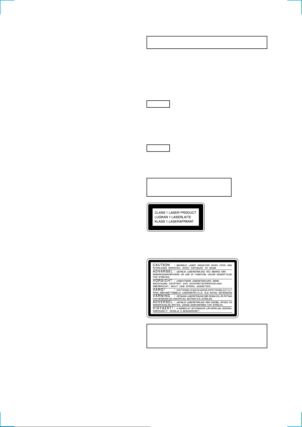
TABLE OF CONTENTS
SECTION 1
SERVICING NOTES
1. SERVICING NOTES ......................................................... 4
2. GENERAL.......................................................................... 12
3. DISASSEMBLY
3-1. Case ..................................................................................... 13
3-2. Front Panel Section ............................................................. 13
3-3. CD Mechanism Deck Section ............................................. 14
3-4. MD Mechanism Deck Block ............................................... 14
3-5. CD Base Unit ...................................................................... 15
3-6. Main Board ......................................................................... 15
3-7. Fitting Base (Guide) Assy, Bracket (Chassis) and
Magnet Assy ....................................................................... 16
3-8. Tray (Sub) ........................................................................... 16
3-9. Chassis (Mold B) Section, Stocker Section and
Slider (Selection) ................................................................ 17
3-10. Gears Installation .............................................................. 17
3-11. Slider (Selection) Installation ............................................ 18
3-12. Stocker Section Installation............................................... 18
3-13. Chassis (Mold B) Section Installation .............................. 19
3-14. MD Mechanism Deck Section .......................................... 19
3-15. BD (MD) Board ................................................................ 20
4. TEST MODE ...................................................................... 21
5. ELECTRICAL ADJUSTMENT.................................... 27
6. DIAGRAMS
6-1. Circuit Boards Location ...................................................... 39
6-2. Block Diagrams ................................................................... 41
6-3. Schematic Diagram – CD Section –.................................... 44
6-4. Printed Wiring Board – CD Section – ................................. 45
6-5. Printed Wiring Board – MD Section – ................................ 46
6-6. Schematic Diagram – MD Section (1/2) – .......................... 47
6-7. Schematic Diagram – MD Section (2/2) – .......................... 48
6-8. Schematic Diagram – Main Section (1/2) – ........................ 49
6-9. Schematic Diagram – Main Section (2/2) – ........................ 50
6-10. Printed Wiring Board – Main Section – ............................ 51
6-11. Schematic Diagram – Digital Section – ............................ 52
6-12. Printed Wiring Board – Digital Section – ......................... 53
6-13. Schematic Diagram – Panel Section – .............................. 54
6-14. Printed Wiring Board – Panel Section – ............................ 55
6-15. Schematic Diagram – CD Mechanism Section – .............. 56
6-16. Printed Wiring Board – CD Mechanism Section – ........... 57
6-17. IC Block Diagrams ............................................................ 58
6-18. IC Pin Function ................................................................. 62
NOTES ON HANDLING THE OPTICAL PICK-UP
BLOCK OR BASE UNIT
The laser diode in the optical pick-up block may suffer electrostatic
break-down because of the potential difference generated by the
charged electrostatic load, etc. on clothing and the human body.
During repair, pay attention to electrostatic break-down and also
use the procedure in the printed matter which is included in the
repair parts.
The flexible board is easily damaged and should be handled with
care.
FOR CD
NOTES ON LASER DIODE EMISSION CHECK
The laser beam on this model is concentrated so as to be focused on
the disc reflective surface by the objective lens in the optical pickup block. Therefore, when checking the laser diode emission, observe from more than 30 cm away from the objective lens.
FOR MD
NOTES ON LASER DIODE EMISSION CHECK
Never look into the laser diode emission from right above when
checking it for adjustment. It is feared that you will lose your sight.
Laser component in this product is capable
of emitting radiation exceeding the limit for
Class 1.
This appliance is classified as a CLASS 1 LASER product. The
CLASS 1 LASER PRODUCT MARKING is located on the rear
exterior.
This caution
label is located
inside the unit.
7. EXPLODED VIEW
7-1. Case, Chassis Section ......................................................... 71
7-2. Front Panel Section ............................................................. 72
7-3. CD Mechanism Deck Section-1 .......................................... 73
7-4. CD Mechanism Deck Section-2 .......................................... 74
7-5. CD Base Unit Section ......................................................... 75
7-6. MD Mechanism Section-1 .................................................. 76
7-7. MD Mechanism Section-2 .................................................. 77
8. ELECTRICAL PARTS LIST ........................................ 78
SAFETY-RELATED COMPONENT WARNING!!
COMPONENTS IDENTIFIED BY MARK 0 OR DOTTED
LINE WITH MARK 0 ON THE SCHEMATIC DIAGRAMS
AND IN THE PARTS LIST ARE CRITICAL TO SAFE
OPERATION. REPLACE THESE COMPONENTS WITH
SONY PARTS WHOSE PART NUMBERS APPEAR AS
SHOWN IN THIS MANUAL OR IN SUPPLEMENTS PUBLISHED BY SONY.
4
CAUTION
Use of controls or adjustments or performance of procedures
other than those specified herein may result in hazardous radiation exposure.
Notes on chip component replacement
• Never reuse a disconnected chip component.
• Notice that the minus side of a tantalum capacitor may be
damaged by heat.
Flexible Circuit Board Repairing
• Keep the temperature of soldering iron around 270˚C
during repairing.
• Do not touch the soldering iron on the same conductor of the
circuit board (within 3 times).
• Be careful not to apply force on the conductor when soldering
or unsoldering.
Page 5
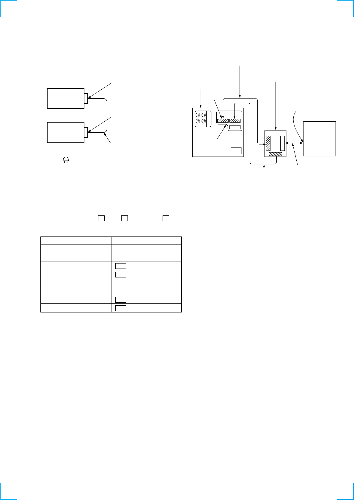
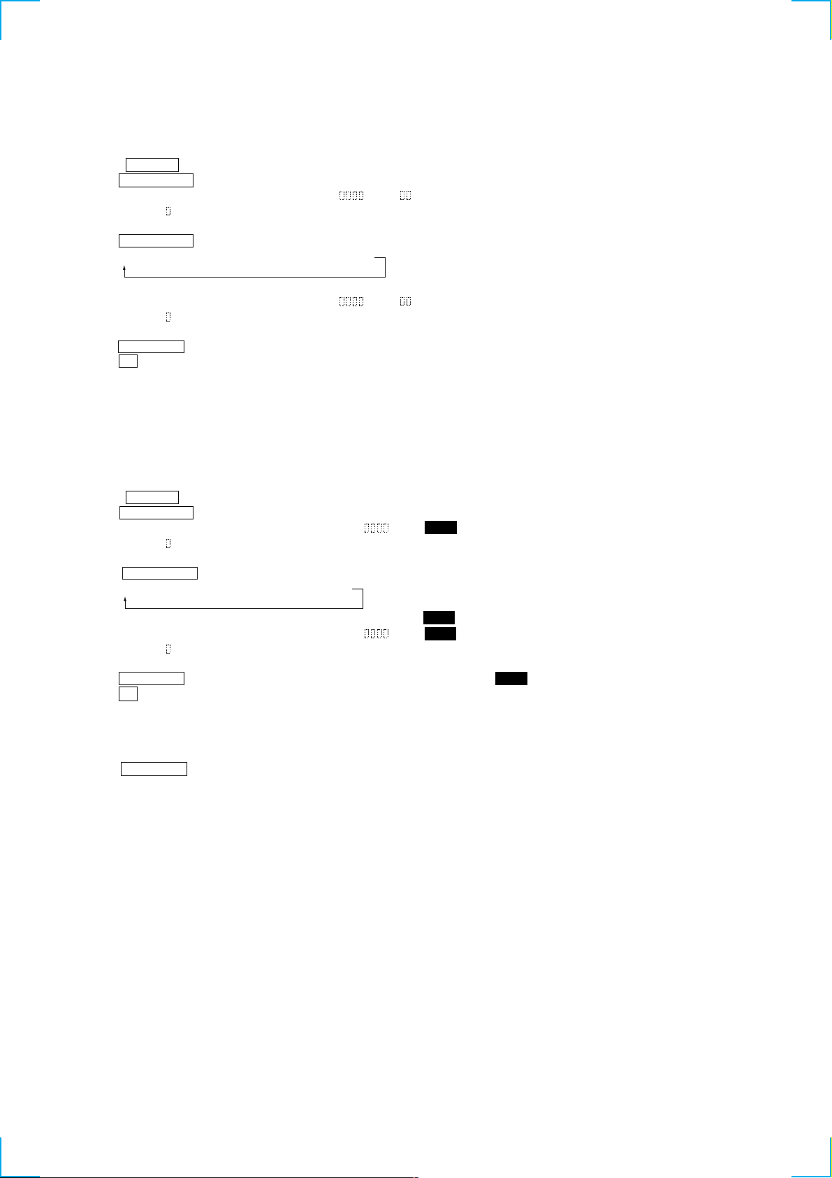
POWER SUPPLY DURING SERVICING
l
Connection:
• As this set has not own power supply, it does not operate independently. Therefore, during servicing, connect it to the Pre-Main
amplifier and Tuner Unit (STR-NX5MD) of DHC-NX5MD.
SYSTEM CONTROL termina
Set
SYSTEM CONTROL terminal
Pre-Main AMP
and Tuner Unit
Connector cable (19P)
AC IN
If STR-NX5MD are not available, use the Power Feed Jig (PFJ-
1) and Relay Connector Jig.
In this case, after turn on the POWER switch on the Power Feed
Jig, supply power with the following methods.
Procedure:
1. Press three buttons of G (MD), A (DISC 1), and s (CD)
simultaneously.
Connector cable (17P) of
attachment to power feed jig
Power feed jig
(PFJ-1)
CDP/MD
P707, P909
Relay connector jig
(J-2501-197-A)
ST
Exclusive cable (15P)
CN101 (19P)
SYSTEM CONTROL
terminal
Set
system cable
function button
CD AMS – AMS –
AMS + AMS +
FR m
FF M
MD AMS – AMS –
AMS + AMS +
FR m
FF M
5
Page 6
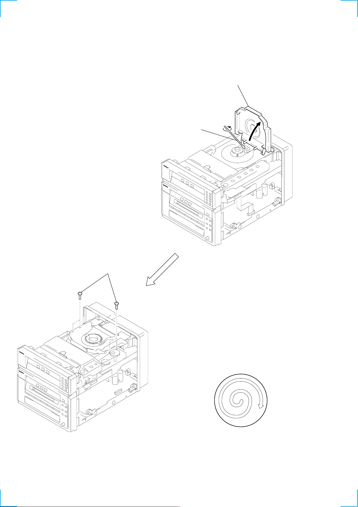
OPTICAL PICK-UP CLEANING
1
Remove the case. (Refer to disassembly page 13)
3 Open the magnet
assy.
4 Cleaning the
optical pick-up.
2 four screws
(BVTP M2.6)
Note 1: In cleaning the lens, do not apply an excessive force.
As the optical pick-up is vulnerable, application of excessive
force could damage the lens holder.
Note 2: In cleaning, do not use a cleaner other than exclusive clean-
ing liquid (KK-91 or isopropyl alcohol).
Note 3: Wipe the objective lens spirally from center toward outside.
(See Figure A)
(Figure A)
6
Page 7
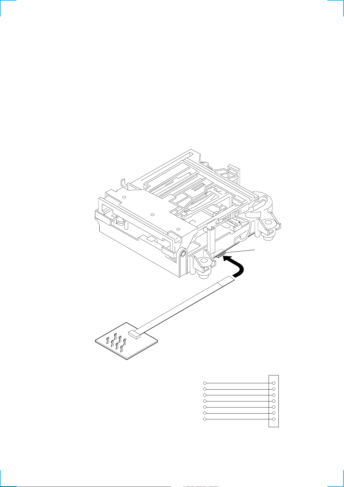
JIG FOR CHECKING BD (MD) BOARD WAVEFORM
The special jig (J-2501-196-A) is useful for checking the waveform of the BD (MD) board. The names of terminals and the checking items
to be performed are shown as follows.
GND : Ground
I+3V : For measuring IOP (Check the deterioration of the optical pick-up laser)
IOP : For measuring IOP (Check the deterioration of the optical pick-up laser)
TE : TRK error signal (Traverse adjustment)
VC : Reference level for checking the signal
RF : RF signal (Check jitter)
FE : Focus error signal
I+3V
GND
FE
RF
IOP
TE
VC
I+3V
IOP
GND
TE
FE
VC
RF
CN105
1
I+3V
IOP
GND
TE
FE
VC
RF
7
for
MDM-7B
7
Page 8

Iop DATA RECORDING AND DISPLAY WHEN OPTICAL PICK-UP AND NON-VOLATILE MEMORY (IC195 OF
BD BOARD) ARE REPLACED
The Iop value labeled on the optical pick-up can be recorded in the non-volatile memory. By recording the value, it will eliminate the need
to look at the value on the label of the optical pick-up. When replacing the optical pick-up or non-volatile memory (IC195 of BD board),
record the Iop value on the optical pick-up according to the following procedure.
Record Precedure:
1. Clicking the ENTER/YES button and the A (DISC 5) button while clicking the m (MD) button causes the program to enter test mode
and the message “Check” to be displayed on screen.
2. Rotate the MD JOG knob to display “[Service]”, and press the ENTER/YES button.
3. Rotate the MD JOG knob to display “Iop Write” (C05), and press the ENTER/YES button.
4. The display becomes “Ref=@@@.@” (@ is an arbitrary number) and the numbers which can be changed will blink.
5. Input the Iop value written on the optical pick-up.
To select the number : Rotate the MD JOG knob.
To select the digit : Press the MD JOG knob.
6. When the ENTER/YES button is pressed, the display becomes “Measu=@@@.@” (@ is an arbitrary number).
7. As the adjustment results are recorded for the 6 value. Leave it as it is and press the ENTER/YES button.
8. “Complete!” will be displayed momentarily. The value will be recorded in the non-volatile memory and the display will become “Iop
Write” (C05).
9. Press the STR REPEAT button to complete.
Display Precedure:
1. Clicking the ENTER/YES button and the A (DISC 5) button while clicking the m (MD) button causes the program to enter test mode
and the message “Check” to be displayed on screen.
2. Rotate the MD JOG knob to display “[Service]”, and press the ENTER/YES button.
3. Rotate the MD JOG knob to display “Iop Read” (C26).
4. “@@.@/##.#” is displayed and the recorded contents are displayed.
@@.@ : indicates the Iop value labeled on the pick-up.
##.# : indicates the Iop value after adjustment
5. To end, press the MD JOG button or MENU/NO button to display “Iop Read” (C26). Then press the REPEAT button.
8
Page 9

CHECKS PRIOR TO PARTS REPLACEMENT AND ADJUSTMENTS
Before performing repairs, perform the following checks to determine the faulty locations up to a certain extent.
Details of the procedures are described in “5 Electrical Adjustments”.
• 5-6-2. Laser power check (see page 31)
• 5-6-3. Iop Compare (see page 31)
• 5-6-4. Auto Check (see page 32)
Note:
The criteria for determination above is intended merely to determine if satisfactory or not, and does not serve as the specified value for
adjustments.
When performing adjustments, use the specified values for adjustments.
9
Page 10
RETRY CAUSE DISPLAY MODE
• In this test mode, the causes for retry of the unit during recording can be displayed on the fluorescent indicator tube. During playback, the
“track mode” for obtaining track information will be set.
This is useful for locating the faulty part of the unit.
• The following will be displayed :
During recording and stop : Retry cause, number of retries, and number of retry errors.
During playback : Information such as type of disc played, part played, copyright.
These are displayed in hexadecimal.
Procedure:
1. Press the ENTER/YES button while pressing the A (DISC 5) button and NAME EDIT/CHARACTER button.
2. Press the REC/RECIT button to start recording. Then press the X button and start recording.
3. To check the “track mode”, press the H button to start play.
4. To exit the test mode, press the @/1 button, and turn OFF the power. When “TOC” disappears, disconnect the power plug from the outlet.
Fig. 1 Reading the Test Mode Display
(During recording and stop)
RTs@@c##c***
Fluorescent display tube display
@@ : Cause of retry
## : Number of retries
*** : Number of retry errors
Reading the Retry Cause Display
Lower Bits
Hexadecimal
Bit
Binary
Higher Bits
84218421
b7 b6 b5 b4 b3 b2 b1 b0
00000001
00000010
00000100
00001000
00010000
00100000
01000000
10000000
Hexa-
decimal
01
02
04
08
10
20
40
80
Fig. 2 Reading the Test Mode Display
(During playback)
@@####**$$
Fluorescent display tube display
@@ : Parts No. (name of area named on TOC)
## : Cluster
** : Sector
$$ : Track mode (Track information such as copyright infor-
Cause of Retry Occurring conditions
shock
ader5
Discontinuous address
DIN unlock
FCS incorrect
IVR rec error
CLV unlock
Access fault
} Address (Physical address on disc)
mation of each part)
When track jump (shock) is detected
When ADER was counted more than five times continu-
ously
When ADIP address is not continuous
When DIN unlock is detected
When not in focus
When ABCD signal level exceeds the specified range
When CLV is unlocked
When access operation is not performed normally
Reading the Display:
Convert the hexadecimal display into binary display. If more than two causes, they will be added.
Example
When 42 is displayed:
Higher bit : 4 = 0100 t b6
Lower bit : 2 = 0010 t b1
In this case, the retry cause is combined of “CLV unlock” and “ader5”.
When A2 is displayed:
Higher bit : A = 1010 t b7+b5
Lower bit : 2 = 0010 t b1
The retry cause in this case is combined of “Access fault”, “IVR rec error”, and “ader5”.
10
Page 11
Reading the Track Mode Display
Higher Bits Lower Bits
Hexadecimal
Bit
Binary
Reading the Display:
Convert the hexadecimal display into binary display. If more than two causes, they will be added.
Example When 84 is displayed:
Higher bit : 8 = 1000 t b7
Lower bit : 4 = 0100 t b2
In this case, as b2 and b7 are 1 and others are 0, it can be determined that the retry cause is combined of “Emphasis OFF”, “Monaural”,
“Original”, “Copyright exists”, and “Write allowed”.
Example When 07 is displayed:
Higher bit : 0 = 1000 t All 0
Lower bit : 7 = 0111 t b0+b1+b2
In this case, as b0, b1, and b2 are 1 and others are 0, it can be determined that the retry cause is combined of “Emphasis ON”, “Stereo”,
“Original”, “Copyright exists”, and “Write prohibited”.
84218421
b7 b6 b5 b4 b3 b2 b1 b0
00000001
00000010
00000100
00001000
00010000
00100000
01000000
10000000
Hexa-
decimal
01
02
04
08
10
20
40
80
When 0 When 1
Emphasis OFF
Monaural
This is 2-bit display. Normally 01.
01:Normal audio. Others:Invalid
Audio (Normal)
Original
Copyright
Write prohibited
Details
Emphasis ON
Stereo
Invalid
Digital copy
No copyright
Write allowed
Hexadecimal t Binary Conversion Table
Hexadecimal Binary Hexadecimal Binary
0
1
2
3
4
5
6
7
0000
0001
0010
0011
0100
0101
0110
0111
8
9
A
B
C
D
E
F
1000
1001
1010
1011
1100
1101
1110
1111
11
Page 12
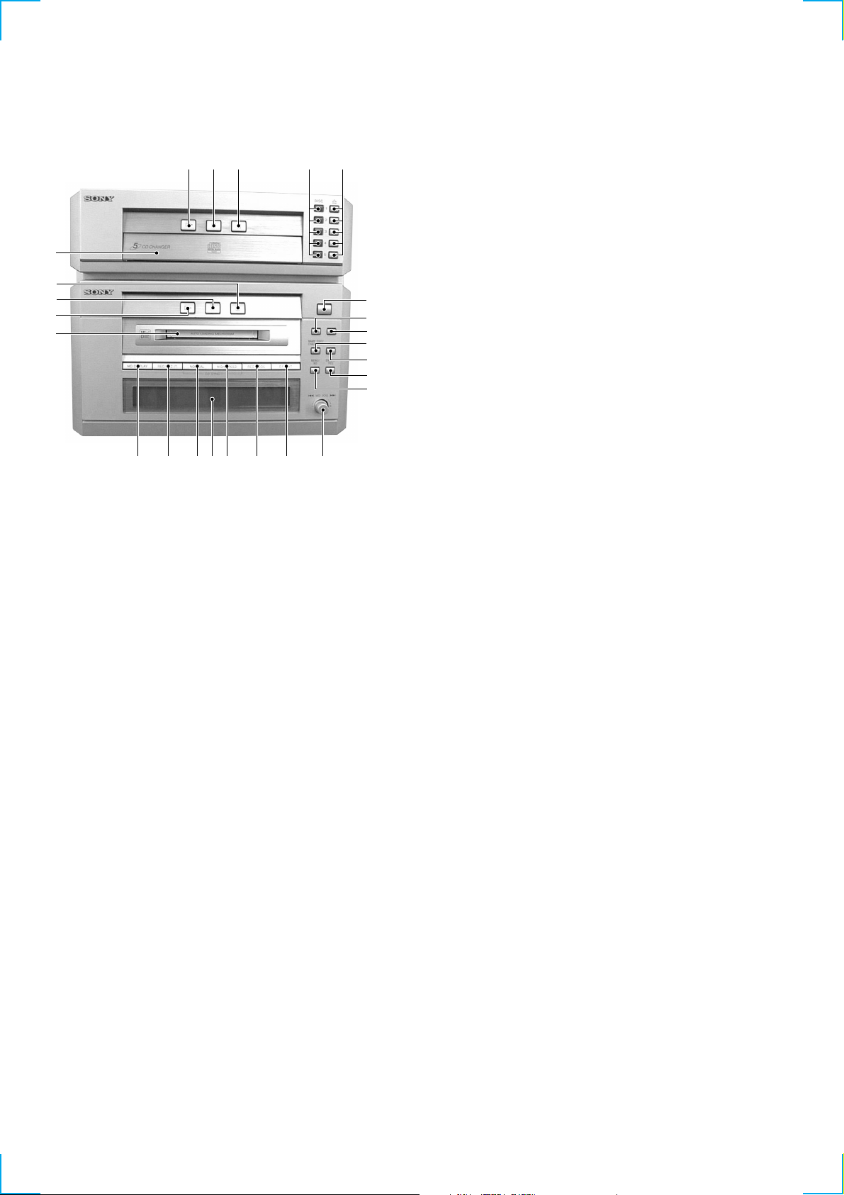
• LOCATION OF CONTROLS
1 2 345
– Front Panel –
wg
wf
wd
ws
wa
SECTION 2
GENERAL
6
7
8
9
q;
qa
qs
qdqfqgqhqjqkqlw;
1 G (CD) button
2 S (CD) button
3 s (CD) button
4 DISC 1 to 5 (CD) button and indicator
5 A (CD DISC 1 to 5) button
6 A (MD) button
7 m (MD) button
8 M (MD) button
9 NAME EDIT/CHARACTER button
q; CLEAR button
qa MENU/NO button
qs ENTER/YES button
qd . MD JOG > +/– dial
qf S.F EDIT button
qg REC MODE button
qh HIGH SPEED button
qj Display window
qk NORMAL button
ql REC/REC IT button
w; MD DISPLAY button
wa MD disc compartment
ws G (MD) button
wd S (MD) button
wf s (MD) button
wg CD disc tray
12
Page 13
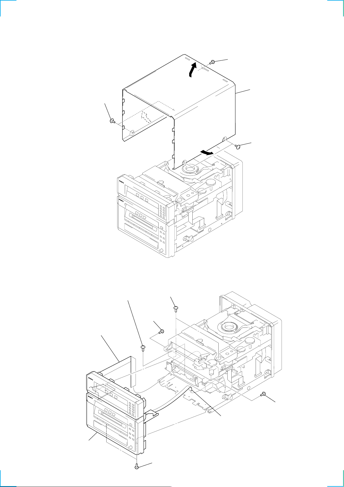
SECTION 3
)
DISASSEMBLY
Note: Follow the disassembly procedure in the numerical order given.
3-1. CASE
2 two screws
(case 3 TP2)
1 screw
(BVTP3 × 10)
A
3 Remove the case
in the arrow A
direction.
2 two screws
(case 3 TP2)
3-2. FRONT PANEL SECTION
1 flat cable (13 core)
(CN103)
5 screw
(BVTP3 × 10)
4 screw
3 two screws
(SUMITITE (B3), +BV)
(BVTP2.6 × 8)
2 flat cable (9 core)
(CN102)
4 screw
(BVTP2.6 × 8
7 front panel
section
6 two screws
(BVTP3 × 10)
13
Page 14
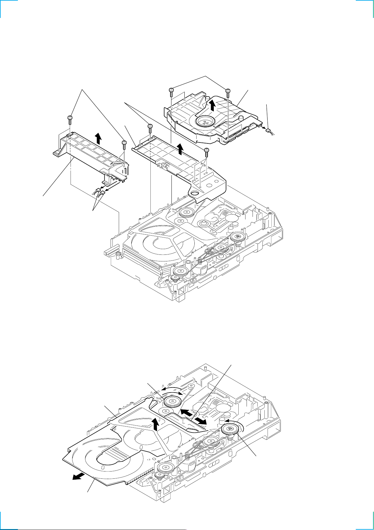
3-3. CD MECHANISM DECK SECTION
)
(CDM53E-K4BD40)
5 Remove the CD mechanism deck
section (CDM53E-K4BD40) in
the arrow A direction.
1 flat cable (17 core)
(CN112)
4 four screws
(BVTP3 × 10)
A
3 connector
(CN713)
3-4. MD MECHANISM DECK BLOCK
2 flat cable (19 core)
(CN111)
2 screw
(BVTP3 × 8)
14
3 MD mechanism
deck block
1 flat cable (25 core
(CN114)
Page 15
3-5. CD BASE UNIT
s
)
(BU-K4BD40)
4 CD base unit
(BU-K4BD40)
3-6. MAIN BOARD
6 Remove the MAIN board
4 three screws
(BVTP3 × 8)
3 two compression springs
(black)
1 two screws
in the arrow A direction.
2 two compression spring
(silver)
1 two screws
(PTPWH M2.6)
(PTPWH M2.6)
A
5 two PC board
holders
2 connection cord
3 screw
(BVTP3 × 10)
1 screw
(BVTP3 × 10
(CN101)
15
Page 16
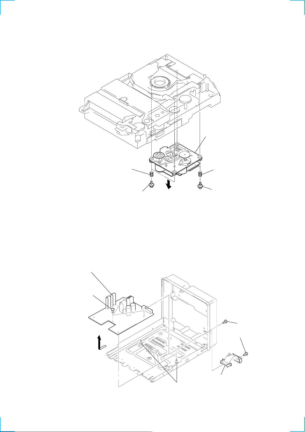
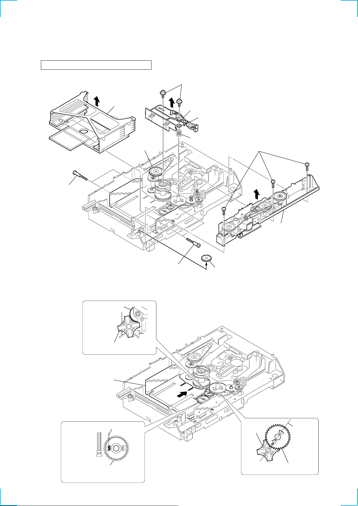
3-7. FITTING BASE (GUIDE) ASSY, BRACKET (CHASSIS) AND
MAGNET ASSY
7 four screws
(BVTP M2.6)
2 four screws
(BVTP M2.6)
4 five screws
(BVTP M2.6)
5 bracket
(chassis)
3 base
(guide) assy, fitting
1 two connectors
(CN709, 715)
8 base (magnet) assy, fitting
6 connector
(CN710)
3-8. TRAY (SUB)
1 Rotating the pulley (LD), shift the slider (selection) in the arrow A direction.
2 Rotating the pulley (mode) in the arrow direction, adjust the tray (sub) to be removed.
3 Rotating the pulley (LD), shift the slider (selection) in the arrow B direction.
4 Rotating the pulley (mode) in the arrow direction, remove the tray (sub) to be removed.
pulley (LD)
stocker
section
tray (sub)
A
B
slider (selection)
pulley (mode)
16
Page 17
3-9. CHASSIS (MOLD B) SECTION, STOCKER SECTION AND
5 stocker
section
4 two step
screws
4 two step screws
3 gear (eject)
2 chassis (mold B) section
Note: Rotating the pulley (LD),
shift the slider (selection)
to the left.
9 compression
spring
7 slider (selection)
8 washer
6 two screws
(PTPWH M2.6)
1 three screws
(BVTP M2.6)
pulley (LD)
SLIDER (SELECTION)
Note: In mounting the parts, refer to page 18 and 19.
3-10. GEARS INSTALLATION
3 gear (gear B)
portion A
Adjust the gear (gear B) with the
portion A as shown.
1 Slide the slider (U/D)
2 gear (U/D slider)
fully in the arrow
direction.
slider (U/D) gear
4 gear (gear A)
gear
(gear B)
linearly
Adjust the gear so that it meshes with
the bottom tooth of slider (U/D)gear,
as shown.
Adjust so as to be aligned with
gear (B) linearly,as shown.
17
Page 18
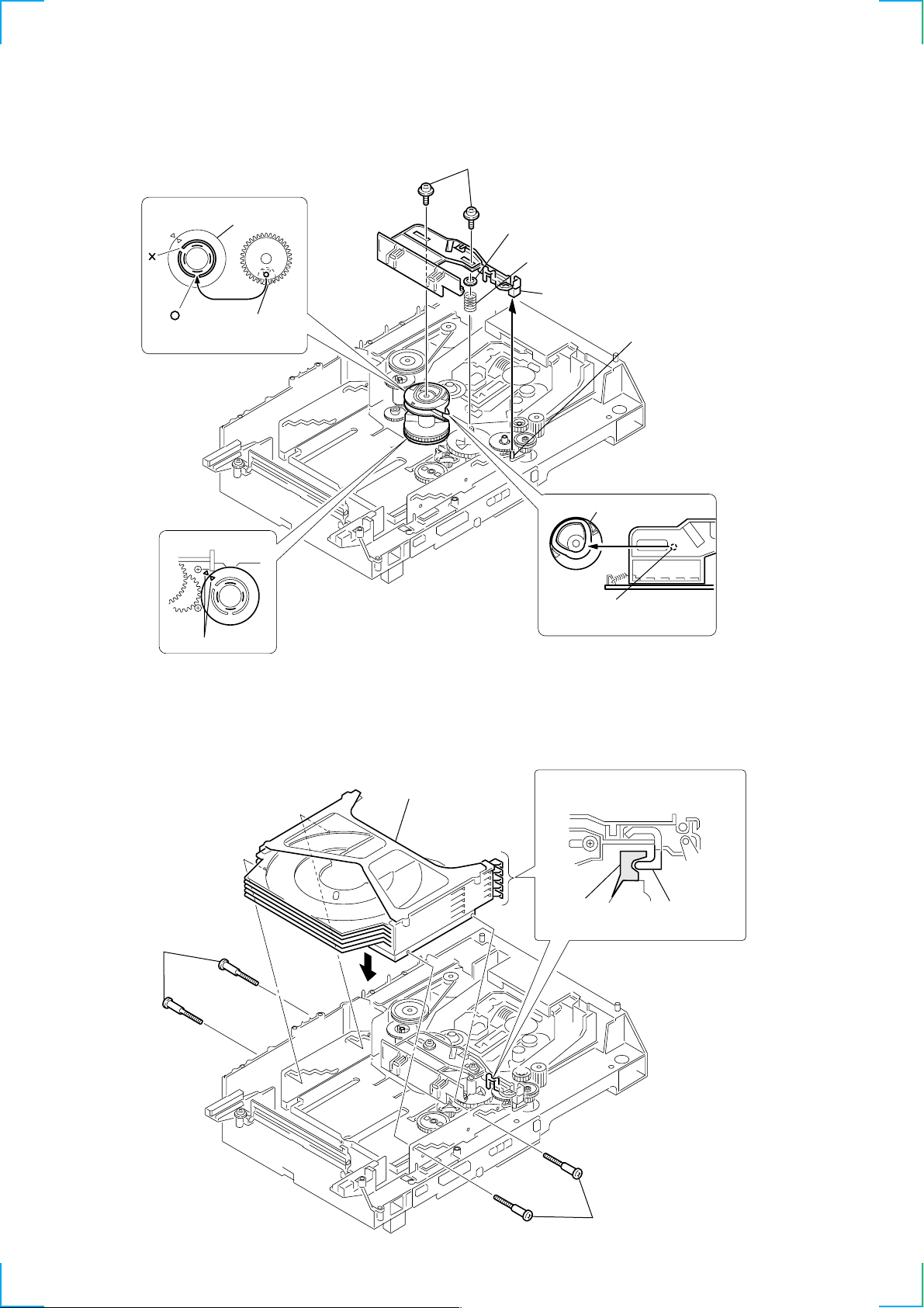
3-11. SLIDER (SELECTION) INSTALLATION
2 gear (chuking)
rotary encoder
Align with the slot of
rotary encoder.
1 rotary encoder
6 two screws
(PTPWH M2.6)
5 washer
4 compression spring
7 Insert the slider (selection)
into the portion A.
portion A
3 convex portion of
slider (selection)
gear (chuking)
align marking
3-12. STOCKER SECTION INSTALLATION
3 two step screws
1 stocker section
Insert a convex portion into
a groove of gear (chuking).
2 portion A of tray (sub)
Hook the portion A of tray (sub)
to the slider (selection).
potion A
of tray (sub)
sticking of
slider (selection)
18
3 two step screws
Page 19
3-13. CHASSIS (MOLD B) SECTION INSTALLATION
n
3 three screws
(BVTP M2.6)
2 Insert the gear (eject)
under the gear (LD
deceleration).
gear (LD deceleration)
3-14. MD MECHANISM DECK SECTION
(MDM-7B)
portion A
portion B of
slider (selection)
1 two screws
(BVTP 3 × 8)
1 Insert the portion A of
chassis (mold B) sectio
into the portion B of
slider (selection).
qa two screws
(BVTPWH M3), step
qs MD mechanism deck
(MDM-7B)
2 screw
(BVTP 3 × 8)
7 two claws
8 DIGITAL board
6 screw
A
3 cover (MD)
4 flat type wire (17core)
(CN1004)
5 flat type wire (27core)
(CN1003)
0 two screws
(BVTPWH M3), step
A
9 flat type wire (25core)
(CN1001)
(BVTP 3 × 8)
19
Page 20
3-15. BD (MD) BOARD
5 Connect the short land
by lead wire.
short land
Bottom of the optical pick-up
2 Remove the solder
2 Remove the solder
(Two portions)
(Two portions)
CN101
3 two screws
(BTP 2 × 6)
6 connector
(CN101)
1 connector
(CN104)
4 BD (MD) board
2 Remove the solder
(Two portions)
M102
M101
M103
S102
2 Remove the solder
(Three portions)
20
Page 21
SECTION 4
TEST MODE
[LED All Lit, Key Check Mode]
Procedure:
1. Press the ?/1 button to turn the power ON.
2. Press three buttons of
simultaneously.
3. LEDs are all turned on.
Press the G (CD) button, and the key check mode is activated.
4. To release from this mode, press three buttons in the same
manner as step 2, or remove the power cord.
[CD Delivery Mode]
• This mode moves the optical pick-up to the position durable to
vibration. Use this mode when returning the set to the customer
after repair.
Procedure:
1. Press the ?/1 button to turn the power ON.
2. Press the G (MD) and [DISC 1] buttons simultaneously.
3. A message “LOCK” is displayed on the liquid crystal display
of the STR-NX5MD, and the CD delivery mode is set.
[CD/MD Test Mode]
(In case of connected to the STR-NX5MD)
• If connected to the STR-NX5MD, the mode also acts as the
STR-NX5MD amplifer test mode.
Procedure:
1. Press the ?/1 button to turn the power ON.
2. Press three buttons of [ENTER/YES] + [DEMO] and [BAND] of
the STR-NX5MD simultaneously.
3. On liquid crystal display of the STR-NX5MD, the disc calendar
blinks, then the function which was set before the test mode
became active is displayed.
G (MD), A (DISC 1), and [DISC 5]
[COLD RESET]
Procedure:
1. Press the ?/1 button to turn the power ON.
2. Press CLEAR (MD) and
s (CD) buttons simultaneously.
[CD/MD Test Mode]
(In case of connected to the power feed jig)
Procedure:
1. Turn on the Power switch on the power feed jig.
2. Press three buttons of G (MD), A (DISC 1), and s (CD)
simultaneously.
3. Also, the other functions are enabled by pressing two buttons
simultaneously.
A combination of respective functions and buttons is as follows.
function button
CD AMS – AMS –
AMS + AMS +
FR m
FF M
MD AMS – AMS –
AMS + AMS +
FR m
FF M
21
Page 22
4-1. PRECAUTIONS FOR USE OF TEST MODE
• As loading related operations will be performed regardless of the test mode operations being performed, be sure to check that the disc
is stopped before setting and removing it.
Even if the A (MD) button is pressed while the disc is rotating during continuous playback, continuous recording, etc., the disc will not
stop rotating.
Therefore, it will be ejected while rotating.
Be sure to press the A (MD) button after pressing the MENU/NO button and the rotation of disc is stopped.
4-1-1. Recording laser emission mode and operating buttons
• Continuous recording mode (CREC 1MODE) (C35)
• Laser power check mode (LDPWR CHECK) (C13)
• Laser power adjustment mode (LDPWR ADJUS) (C04)
• Iop check (Iop Compare) (C27)
• Iop value nonvolatile writing (Iop NV Save) (C06)
• Traverse (MO) check (EF MO CHECK) (C14)
• Traverse (MO) adjustment (EF MO ADJUS) (C07)
• When pressing the REC MODE button.
4-2. SETTING THE TEST MODE
The following are two methods of entering the test mode.
Procedure: Pressing the ENTER/YES button and the A (DISC 5) button while pressing the m (MD) button causes the program to
enter test mode.
When the test mode is set, “[Check]” will be displayed. Rotating the MD JOG knob switches between the following three
groups; ··· y Check y Service y Develop y ···.
NOTE: Do not use the test mode in the [Develop] group.
If used, the unit may not operate normally.
If the [Develop] group is set accidentally, press the MENU/NO button immediately to exit the [Develop] group.
4-3. EXITING THE TEST MODE
Press the REPEAT button. The disc is ejected when loaded, and “Standby” display blinks, and the STANDBY state is set.
4-4. BASIC OPERATIONS OF THE TEST MODE
All operations are performed using the MD JOG knob, ENTER/YES button, and MENU/NO button.
The functions of these buttons are as follows.
Function name
MENU/NO button
ENTER/YES button
AMS
knob
Left or Right
Push
Cancel or move to top hierarchy
Set
Select
Set submenu
Function
22
Page 23
4-5. SELECTING THE TEST MODE
There are 26 types of test modes as shown below. The groups can be switched by rotating the MD JOG knob. After selecting the group to be
used, press the ENTER/YES button. After setting a certain group, rotating the MD JOG knob switches between these modes.
Refer to “Group” in the table for details selected.
All adjustments and checks during servicing can be performed in the test mode in the Service group.
NOTE: Do not use the test mode in the [Develop] group.
If used, the unit may not operate normally.
If the [Develop] group is set accidentally, press the MENU/NO button immediately to exit the [Develop] group.
Display
AUTO CHECK
Err Display
TEMP ADJUS
LDPWR ADJUS
Iop Write
Iop NV Save
EF MO ADJUS
EF CD ADJUS
FBIAS ADJUS
AG Set (MO)
AG Set (CD)
TEMP CHECK
LDPWR CHECK
EF MO CHECK
EF CD CHECK
FBIAS CHECK
ScurveCHECK
VERIFYMODE
DETRK CHECK
0920 CHECK
Iop Read
Iop Compare
ADJ CLEAR
INFORMATION
CPLAY1MODE
CREC 1MODE
No.
Automatic self-diagnosis
C01
Error history display, clear
C02
Temperature compensation offset adjustment
C03
Laser power adjustment
C04
Iop data writing
C05
Writes current Iop value in read nonvolatile memory using microprocessor
C06
Traverse (MO) adjustment
C07
Traverse (CD) adjustment
C08
Focus bias adjustment
C09
Focus, tracking gain adjustment (MO)
C10
Focus, tracking gain adjustment (CD)
C11
Temperature compensation offset check
C12
Laser power check
C13
Traverse (MO) check
C14
Traverse (CD) check
C15
Focus bias check
C16
S-curve check
C17
Nonvolatile memory check
C18
Detrack check
C19
Most circumference check
C25
Iop data display
C26
Comparison with initial Iop value written in nonvolatile memory
C27
Initialization of nonvolatile memory for adjustment values
C28
Display of microprocessor version, etc.
C31
Continuous playback mode
C34
Continuous recording mode
C35
Details
Mark
Group
Check Service
• For details of each adjustment mode, refer to “5. Electrical Adjustments”.
For details of “Err Display”, refer to “Self-Diagnosis Function” on page 2.
• If a different mode has been selected by mistake, press the MENU/NO button to exit that mode.
• Modes with (X) in the Mark column are not used for servicing and therefore are not described in detail. If these modes are set acciden-
tally, press the MENU/NO button to exit the mode immediately.
23
Page 24
4-5-1. Operating the Continuous Playback Mode
1. Entering the continuous playback mode
1 Set the disc in the unit. (Whichever recordable discs or discs for playback only are available.)
2 Rotate the MD JOG knob and display “CPLAY1MODE” (C34).
3 Press the ENTER/YES button to change the display to “CPLAY1 MID”.
4 When access completes, the display changes to “C = AD = ”.
Note : The numbers “ ” displayed show you error rates and ADER.
2. Changing the parts to be played back
1 Press the ENTER/YES button during continuous playback to change the display as below.
“CPLAY1 MID” t “CPLAY1 OUT” t “CPLAY1 IN”
When pressed another time, the parts to be played back can be moved.
2 When access completes, the display changes to “C = AD = ”.
Note : The numbers “ ” displayed show you error rates and ADER.
3. Ending the continuous playback mode
1 Press the MENU/NO button. The display will change to “CPLAY1MODE”(C34).
2 Press the A (MD) button to remove the disc.
Note : The playback start addresses for IN, MID, and OUT are as follows.
IN 40h cluster
MID 300h cluster
OUT 700h cluster
4-5-2. Operating the Continuous Recording Mode (Use only when performing self-recording/palyback check.)
1. Entering the continuous recording mode
1 Set a recordable disc in the unit.
2 Rotate the MD JOG knob and display “CREC 1MODE” (C35).
3 Press the ENTER/YES button to change the display to “CREC1 MID”.
4 When access completes, the display changes to “CREC1 ( )” and REC lights up.
Note : The numbers “ ” displayed shows you the recording position addresses.
2. Changing the parts to be recorded
1 When the ENTER/YES button is pressed during continuous recording, the display changes as below.
“CREC1 MID” t “CREC1 OUT” t “CREC1 IN”
When pressed another time, the parts to be recorded can be changed. REC goes off.
2 When access completes, the display changes to “CREC1 (
Note : The numbers “ ” displayed shows you the recording position addresses.
3. Ending the continuous recording mode
1 Press the MENU/NO button. The display changes to “CREC 1MODE” (C35 ) and REC goes off.
2 Press the A (MD) button to remove the disc.
Note 1 : The recording start addresses for IN, MID, and OUT are as follows.
IN 40h cluster
MID 300h cluster
OUT 700h cluster
Note 2 : The MENU/NO button can be used to stop recording anytime.
Note 3 : Do not perform continuous recording for long periods of time above 5 minutes.
Note 4 : During continuous recording, be careful not to apply vibration.
)” and REC lights up.
24
Page 25
4-6. FUNCTIONS OF OTHER BUTTONS
ENTER/YES
s
M (MD JOG)
m (MD JOG)
REC MODE
REC
CLEAR
A
Function
Sets continuous playback when pressed in the STOP state. When pressed during continuous
playback, the tracking servo turns ON/OFF.
Stops continuous playback and continuous recording.
The sled moves to the outer circumference only when this is pressed.
The sled moves to the inner circumference only when this is pressed.
Switches between the pit and groove modes when pressed.
Switches the spindle servo mode (CLV S y CLV A).
Switches the displayed contents each time the button is pressed.
Ejects the disc.
Exits the test mode.
Contents
4-7. TEST MODE DISPLAYS
Each time the MD DISPLAY button is pressed, the display changes in the following order.
When CPLAY and CREC are started, the display will forcibly be switched to the error rate display as the initial mode.
1. Mode display
Displays “TEMP ADJUS” (C03), “CPLAY1MODE” (C34), etc.
2. Error rate display
Displays the error rate in the following way.
C1 = AD =
C1 = Indicates the C1 error.
AD = Indicates ADER.
3. Address display
The address is displayed as follows. (MO:recordable disc, CD:playback only disc)
If the CLEAR button is pressed after pressing the PROGRAM button, the display
switches from groove to pit or vice versa.
h = s = (MO pit and CD)
h = a = (MO groove)
h = Indicates the header address.
s = Indicates the SUBQ address.
a = Indicates the ADIP address.
Note: “–” is displayed when the address cannnot be read.
Auto gain display (Not used in servicing)
Detrack check display (Not used in servicing)
IVR display (Not used in servicing)
Mode display
Error rate display
Address display
C1 error and Jitter display
(Not used in servicing)
AD error and Jitter display
(Not used in servicing)
25
Page 26
4-8. MEANINGS OF OTHER DISPLAYS
Display
G
S
REC
SYNC
L.SYNC
OVER
B/1
A-/REP
TRACK/(LP) 4/Calendar frame
DISC/LP2
SLEEP/SHUF
MONO
When Lit When Off
Servo ON
Tracking servo OFF
Recording mode ON
CLV low speed mode
ABCD adjustment completed
Tracking offset cancel ON
Tracking auto gain OK
Focus auto gain OK
Pit
High reflection
CLV S
CLV LOCK
Contents
Servo OFF
Tracking servo ON
Recording mode OFF
CLV normal mode
Tracking offset cancel OFF
Groove
Low reflection
CLV A
CLV UNLOCK
4-9. AUTOMATIC SELF-DIAGNOSIS FUNCTION
This test mode performs CREC and CPLAY automatically for mainly checking the characteristics of the optical pick-up.
To perform this test mode, the laser power must first be checked.
Perform AUTO CHECK after the laser power check and Iop check.
Procedure
1. Press the ENTER/YES button. If “LDPWR” is displayed, it means that the laser power check has not been performed. In this case, perform
the laser power check and Iop compare, and then repeat from step 1.
2. If a disc is in the mechanical deck, it will be ejected forcibly.
“DISC IN” will be displayed in this case. Load a test disc (MDW-74/GA-1) which can be recorded.
3. If a disk is loaded at step 2, the check will start automatically.
4. When “XX CHECK” is displayed, the item corresponding to XX will be performed.
When “06 CHECK” completes, the disc loaded at step 2 will be ejected. “DISC IN” will be displayed. Load the check disc (MD) TDYS-1.
5. When the disc is loaded in step 4, the check will automatically be resumed from “07 CHECK”.
6. After completing to test item 12, check OK or NG will be displayed. If all items are OK, “CHECK ALL OK” will be displayed. If any item
is NG, it will be displayed as “NG:xxxx”.
When “CHECK ALL OK” is displayed, it means that the optical pick-up is normal. Check the operations of the other spindle motor, thread
motor, etc.
When displayed as “NG:xxxx”, it means that the optical pick-up is faulty. In this case, replace the optical pick-up.
4-10. INFORMATION
Display the software version.
Procedure
1. If displayed as “INFORMATION”, press the ENTER/YES button.
2. The software version will be displayed.
3. Press the MENU/NO button to end this mode.
4-11. WHEN MEMORY NG IS DISPLAYED
If the nonvolatile memory data is abnormal, “E001”/”MEMORY NG” will be displayed so that the MD deck does not continue operations.
In this case, set the test mode promptly and perform the following procedure.
Procedure
1. Set the test mode. (Refer to 4-2.)
2. Normally a message for selecting the test mode will be displayed. However if the nonvolatile memory is abnormal, the following will be
displayed. “INIT EEP?”
3. Press the s button and A button together.
4. Rotate the MD JOG knob and select MDM-7B.
5. Press the MD JOG knob. If the nonvolatile memory is successfully overwritten, the normal test mode will be set and a message to select
the test mode will be displayed.
26
Page 27

SECTION 5
+
–
BD (CD) board
TP (RF)
TP (VC)
oscilloscope
V
e
TP
(VC)
TP
(RF)
TP
(TEO)
TP
(FEO)
TP
(GND)
TP
(AGCCON)
IC102
ELECTRICAL ADJUSTMENTS
CD SECTION
Note:
1. CD Block is basically designed to operate without adjustment. Therefore, check each item in order given.
2. Use YEDS-18 disc (3-702-101-01) unless otherwise indicated.
3. Use an oscilloscope with more than 10 MΩ impedance.
4. Clean the object lens by an applicator with neutral detergent when the
signal level is low than specified value with the following checks.
5. Use the following extension cables and relay connector.
• Extension cable (19P) (Part No. J-2501-011-B)
Relay connector (Part No. J-2501-167-A)
(BD (CD) board CN101 to MAIN board CN111)
• Extension cable (17P) (with connector) (Part No. J-2501-167-A)
(CONNECTOR board CN701 to MAIN board CN301)
1. S-CURVE CHECK
oscilloscop
BD (CD) board
TP (FEO)
TP (VC)
Procedure:
1. Connect oscilloscope to TP (FEO).
2. Connect between TP (FEO) and TP (VC) by lead wire.
3. Connect between TP (AGCCON) and TP (GND) by lead wire.
4. Turn the power ON.
5. Load a disc (YEDS-18) and turn the power ON again and actuate the focus search. (Actuate the focus search when disc tray
is moving in and out)
6. Check the oscilloscope waveform (S-curve) is symmetrical between A and B. And confirm peak to peak level within 2.4±0.7
Vp-p.
S-curve waveform
+
–
symmetry
2. RF LEVEL CHECK
Procedure:
1. Connect oscilloscope to TP (RF).
As TP (RF) and TP (VC) are located at the edge of board, clip
them together with the board using alligator clips.
2. Turn the power ON.
3. Load a disc (YEDS-18) and playback.
4. Confirm that oscilloscope waveform is clear and check RF signal level is correct or not.
Note: Clear RF signal waveform means that the shape “ ” can be clearly
distinguished at the center of the waveform.
RF signal waveform
VOLT/DIV: 200 m
TIME/DIV: 500 ns
level:
1.2 ± 0.2 Vp-p
Connecting points :
[ BD (CD) BOARD ] — SIDE B —
A
within 2.4 ± 0.7 Vp-p
B
7. After check, remove the lead wire connected in step 2.
Note: • Try to measure several times to make sure than the ratio of A : B
or B : A is more than 10 : 7.
• Take sweep time as long as possible and light up the brightness
to obtain best waveform.
27
Page 28

MD SECTION
5-1. PARTS REPLACEMENT AND ADJUSTMENT
If malfunctions caused by the optical pick-up such as sound skipping are suspected, follow the following check.
Check before replacement
Start
5-6-2.
Laser Power Check
(See page 31)
OK
5-6-3.
Iop Compare
(See page 31)
OK
5-6-4.
Auto Check
(See page 32)
OK
Other faults are suspected.
Check the threading mechanism, etc.
NG
NG
NG
Replace the optical pick-up or MDM-7B
28
Page 29

Adjustment flow
Start
Replace IC195
NO
Replace OP or IC195
NO
Replace IC101, IC195, or D101
NO
Replace OP, IC190, or IC195
NO
YES
YES
YES
YES
• Abbreviation
OP: Optical pick-up
After turning off and then on the power,
initialize the EEPROM
For details, refer to 4-11. WHEN MEMORY NG IS
DISPLAYED (See page 26)
5-7. INITIAL SETTING OF ADJUSTMENT VALUE
(See page 34)
5-9. TEMPERATURE COMPENSATION OFFSET
ADJUSTMENT (See page 34)
5-10. LASER POWER ADJUSTMENT (See page 34)
Replace OP, IC102, IC190,
or IC195
NO
Replace OP, IC101, IC151,
or IC195
NO
Replace OP
NO
Replace the spindle motor
NO
5-6-4. Auto Check
(See page 32)
YES
YES
YES
YES
5-11. Iop NV SAVE (See page 35)
5-12. TRAVERSE ADJUSTMENT (See page 35)
5-13. FOCUS BIAS ADJUSTMENT (See page 36)
5-16. AUTO GAIN CONTROL OUTPUT LEVEL
ADJUSTMENT (See page 37)
OP change in Err Display mode
Iop write
Spdl change in Err Display mode
End adjustments
29
Page 30

5-2. PRECAUTIONS FOR CHECKING LASER DIODE
EMISSION
To check the emission of the laser diode during adjustments, never
view directly from the top as this may lose your eye-sight.
5-3. PRECAUTIONS FOR USE OF OPTICAL PICK-
UP (KMS-260B)
As the laser diode in the optical pick-up is easily damaged by static
electricity, solder the laser tap of the flexible board when using it.
Before disconnecting the connector, desolder first. Before connecting the connector, be careful not to remove the solder. Also take
adequate measures to prevent damage by static electricity. Handle
the flexible board with care as it breaks easily.
pick-up
laser tap
Optical pick-up flexible board
flexible board
5-4. PRECAUTIONS FOR ADJUSTMENTS
1) When replacing the following parts, perform the adjustments
and checks with
2) Set the test mode when performing adjustments.
After completing the adjustments, exit the test mode.
Perform the adjustments and checks in “group S” of the test mode.
3) Perform the adjustments to be needed in the order shown.
4) Use the following tools and measuring devices.
• Check Disc (MD) TDYS-1
(Parts No. 4-963-646-01)
• Test Disk (MDW-74/GA-1) (Parts No. 4-229-747-01)
• Laser power meter LPM-8001 (Parts No. J-2501-046-A)
or
MD Laser power meter 8010S (Parts No. J-2501-145-A)
• Oscilloscope (Measure after performing CAL of prove.)
• Digital voltmeter
• Thermometer
• Jig for checking BD board waveform
(Parts No. : J-2501-196-A)
5-7. Initial setting of adjustment values
5-8. Recording of Iop information
5-9. TEMP ADJUST
5-10. Laser power adjustment
5-11. Iop NV Save
5-12. Traverse adjustment
5-13. Focus bias adjustment
5-16. Auto gain adjustment
5-6-4. AUTO CHECK
in the order shown in the following table.
Adjustment
Optical
Pick-up
IC101 IC102 IC151 IC190 IC195 D101
5) When observing several signals on the oscilloscope, etc.,
make sure that VC and ground do not connect inside the oscilloscope.
(VC and ground will become short-circuited.)
6) Using the above jig enables the waveform to be checked without
the need to solder.
(Refer to Servicing Note on page 7.)
7) As the disc used will affect the adjustment results, make sure
that no dusts nor fingerprints are attached to it.
Parts to be replaced
30
Page 31

5-5. USING THE CONTINUOUSLY RECORDED DISC
r
* This disc is used in focus bias adjustment and error rate check.
The following describes how to create a continuous recording
disc.
1. Insert a disc (blank disc) commercially available.
2. Rotate the MD JOG knob and display “CREC 1MODE” (C35).
3. Press the ENTER/YES button again to display “CREC1 MID”.
Display “CREC (0300)” and start to recording.
4. Complete recording within 5 minutes.
5. Press the MENU/NO button and stop recording .
6. Press the AEJECT button and remove the disc.
The above has been how to create a continuous recorded data for
the focus bias adjustment and error rate check.
Note :
• Be careful not to apply vibration during continuous recording.
5-6. CHECKS PRIOR TO REPAIRS
These checks are performed before replacing parts according to
“approximate specifications” to determine the faulty locations. For
details, refer to “Checks Prior to Parts Replacement and Adjustments” (See page 9).
5-6-1. Temperature Compensation Offset Check
When performing adjustments, set the internal temperature and room
temperature to 22 to 28ºC.
Checks cannot be performed properly if performed after some time
from power ON due to the rise in the temperature of the IC and
diode, etc. So, perform the checks again after waiting some time.
Checking Procedure:
1. Rotate the MD JOG knob to display “TEMP CHECK” (C12).
2. Press the ENTER/YES button.
3. “T=@@(##) [OK]” should be displayed. If “T=@@ (##) [NG]”
is displayed, it means that the results are bad.
(@@ indicates the current value set, and ## indicates the value
written in the non-volatile memory.)
5-6-2. Laser Power Check
Before checking, check the Iop value of the optical pick-up.
(Refer to 5-8. Recording and Displaying the Iop Information.)
Connection :
Laser power
meter
Optical pick-up
objective lens
Digital volt mete
BD (MD) board
CN105 pin 1 (I+3V)
CN105 pin 2 (IOP)
Checking Procedure:
1. Set the laser power meter on the objective lens of the optical
pick-up. (When it cannot be set properly, press the m button
or M button to move the optical pick-up.)
Connect the digital volt meter to CN105 pin 1 (I+3V) and
CN105 pin 2 (IOP).
2. Then, rotate the MD JOG knob and display “LDPWR CHECK”
(C13).
3. Press the ENTER/YES button once and display “LD 0.9 mW $
”. Check that the reading of the laser power meter become
0.84 to 0.92 mW.
4. Press the ENTER/YES button once more and display “ LD 7.0
mW $ ”. Check that the reading the laser power meter and
digital volt meter satisfy the specified value.
Specified Value :
Laser power meter reading : 7.0 ± 0.2 mW
Digital voltmeter reading : optical pick-up displayed value ± 10%
(Optical pick-up label)
KMS
260B
20101
H0576
R
Iop = 57.6 mA in this case
Iop (mA) = Digital voltmeter reading (mV)/1 (Ω)
(For details of the method for checking
this value, refer to “5-8. Recording and
Displaying the Iop Information”.)
5. Press the MENU/NO button and display “LDPWR CHECK”
(C13) and stop the laser emission.
(The MENU/NO button is effective at all times to stop the laser
emission.)
Note 1: After step 4, each time the ENTER/YES button is pressed,
the display will be switched between “LD 0.7 mW $ ”,
“LD 6.2 mW $ ”, and “LD Wp $ ”. Nothing needs to
be performed here.
5-6-3. Iop Compare
The current Iop value at laser power 7 mw output and reference Iop
value (set at shipment) written in the nonvolatile memory are
compared, and the rate of increase/decrease will be displayed in
percentage.
Note: Perform this function with the optical pick-up set at room
temperature.
Procedure
1. Rotate the MD JOG knob to display “Iop Compare” (C27).
2. Press the ENTER/YES button and start measurements.
3. When measurements complete, the display changes to
“±xx%yy”.
xx is the percentage of increase/decrease, and OK or NG is
displayed at yy to indicate whether the percentage of increase/
decrease is within the allowable range.
4. Press the MENU/NO button to end.
31
Page 32

e
5-6-4. Auto Check
This test mode performs CREC and CPLAY automatically for
mainly checking the characteristics of the optical pick-up. To
perform this test mode, the laser power must first be checked.
Perform Auto Check after the laser power check and Iop compare.
Procedure
1. Press the ENTER/YES button. If “LDPWR minicheck” is
displayed, it means that the laser power check has not been
performed. In this case, perform the laser power check and Iop
compare, and then repeat from step 1.
2. If a disc is in the mechanical deck, it will be ejected forcibly.
“DISC IN” will be displayed in this case. Load a test disc (MDW74/GA-1) which can be recorded.
3. If a disk is loaded at step 2, the check will start automatically.
4. When “XX CHECK” is displayed, the item corresponding to
XX will be performed.
When “06 CHECK” completes, the disc loaded at step 2 will be
ejected. “DISC IN” will be displayed. Load the check disc (MD)
TDYS-1.
5. When the disc is loaded, the check will automatically be resumed
from “07 CHECK”.
6. After completing to test item 12, check OK or NG will be
displayed. If all items are OK, “CHECK ALL OK” will be
displayed. If any item is NG, it will be displayed as “NG:xxxx”.
When “CHECK ALL OK” is displayed, it means that the optical
pick-up is normal. Check the operations of the other spindle motor,
thread motor, etc.
When displayed as “NG:xxxx”, it means that the optical pick-up is
faulty. In this case, replace the optical pick-up.
5-6-5. Other Checks
All the following checks are performed by the Auto Check mode.
They therefore need not be performed in normal operation.
5-6-6. Traverse Check
5-6-7. Focus Bias Check
5-6-8. C PLAY Check
5-6-9. Self-Recording/Playback Check
6. Observe the waveform of the oscilloscope, and check that the
specified value is satisfied. Do not rotate the MD JOG knob.
(Read power traverse checking)
(Traverse Waveform)
A
VC
B
Specified value : Below 10% offset value
Offset value (%) = X 100
IA – BI
2 (A + B)
7. Press the ENTER/YES button and display “EFB = MO-W”.
8. Observe the waveform of the oscilloscope, and check that the
specified value is satisfied. Do not rotate the MD JOG knob.
(Write power traverse checking)
(Traverse Waveform)
A
VC
B
Specified value : Below 10% offset value
Offset value (%) = X 100
IA – BI
2 (A + B)
9. Press the ENTER/YES button display “EFB = MO-P”.
Then, the optical pick-up moves to the pit area automatically
and servo is imposed.
10. Observe the waveform of the oscilloscope, and check that the
specified value is satisfied. Do not rotate the MD JOG knob.
5-6-6. Traverse Check
Connection :
Oscilloscope
BD (MD) board
CN105 pin 4 (TE)
CN105 pin 6 (VC)
V : 0.5 V/div
H : 10 ms/div
Input : DC mod
Checking Procedure:
1. Connect an oscilloscope to CN105 pin 4 (TE) and CN105 pin
6 (VC) of the BD (MD) board.
2. Load a test disc (MDW-74/GA-1). (Refer to Note 1.)
3. Press the M button and move the optical pick-up outside the
pit.
4. Rotate the MD JOG knob and display “EF MO CHECK” (C14).
5. Press the ENTER/YES button and display “EFB = MO-R”.
(Laser power READ power/Focus servo ON/tracking servo OFF/
spindle (S) servo ON)
(Traverse Waveform)
A
VC
B
Specified value : Below 10% offset value
Offset value (%) = X 100
IA – BI
2 (A + B)
11. Press the ENTER/YES button display “EF MO CHECK” (C14)
The disc stops rotating automatically.
12. Press the A button and remove the disc.
13. Load the check disc (MD) TDYS-1.
14. Roteto the MD JOG knob and display “EF CD CHECK” (C15).
15. Press the ENTER/YES button and display “EFB = CD”.
Servo is imposed automatically.
32
Page 33

e
16. Observe the waveform of the oscilloscope, and check that the
specified value is satisfied. Do not rotate the MD JOG knob.
(Traverse Waveform)
A
VC
B
Specified value : Below 10% offset value
Offset value (%) = X 100
IA – BI
2 (A + B)
17. Press the ENTER/YES button and display “EF CD CHECK”
(C15).
18. Press the A button and remove the check disc (MD) TDYS-1.
Note 1 : MO reading data will be erased during if a recorded disc is
used in this adjustment.
Note 2 : If the traverse waveform is not clear, connect the oscillo-
scope as shown in the following figure so that it can be
seen more clearly.
Oscilloscop
5-6-8. C PLAY Check
MO Error Rate Check
Checking Procedure :
1. Load a continuously recorded test disc (MDW-74/GA-1).
(Refer to “5-5. Using the Continuously Recorded Disc”.)
2. Rotate the MD JOG knob and display “CPLAY1MODE” (C34).
3. Press the ENTER/YES button and display “CPLAY1 MID”.
4. The display changes to “C1 = AD = ”.
5. If the C1 error rate is below 20, check that ADER is 00.
6. Press the MENU/NO button, stop playback, press the A button, and test disc.
CD Error Rate Check
Checking Procedure :
1. Load a check disc (MD) TDYS-1.
2. Rotate the MD JOG knob and display “CPLAY1MODE” (C34).
3. Press the ENTER/YES button twice and display “CPLAY1 MID”.
4. The display changes to “C1 = AD = ”.
5. Check that the C1 error rate is below 20.
6. Press the MENU/NO button, stop playback, press the A button, and the test disc.
5-6-9. Self-Recording/playback Check
Prepare a continuous recording disc using the unit to be repaired
and check the error rate.
BD (MD) board
CN105 pin 4 (TE)
CN105 pin 6 (VC)
330 kΩ
10pF
5-6-7. Focus Bias Check
Change the focus bias and check the focus tolerance amount.
Checking Procedure :
1. Load a continuously recorded test disc (MDW-74/GA-1).
(Refer to “5-5. Using the Continuously Recorded Disc”.)
2. Rotate the MD JOG knob and display “CPLAY 1MODE” (C34).
3. Press the ENTER/YES button and display “CPLAY1 MID”.
4. Press the MENU/NO button when “C = AD = ” is
displayed.
5. Rotate the MD JOG knob and display “FBIAS CHECK” (C16).
6. Press the ENTER/YES button and display “ / c = ”.
The first four digits indicate the C1 error rate, the two digits
after [/] indicate ADER, and the 2 digits after [c =] indicate the
focus bias value.
Check that the C1 error is below 20 and ADER is below 2.
7. Press the ENTER/YES button and display “ / b = ”.
Check that the C1 error is below 100 and ADER is below 2.
8. Press the ENTER/YES button and display “ / a = ”.
Check that the C1 error is below 100 and ADER is below 2.
9. Press the MENU/NO button, next press the A button, and
remove the test disc.
Checking Procedure :
1. Insert a recordable test disc (MDW-74/GA-1) into the unit.
2. Rotate the MD JOG knob to display “CREC 1MODE” (C35).
3. Press the ENTER/YES button to display the “CREC1 MID”.
4. When recording starts, “ REC ” is displayed, this becomes
“CREC (@@@@)” (@@@@ is the address), and recording
starts.
5. About 1 minute later, press the MENU/NO button to stop
continuous recording.
6. Rotate the MD JOG knob to display “CPLAY1MODE” (C34).
7. Press the ENTER/YES button to display “C PLAY1 MID”.
8. “C1 =
AD = ” will be displayed.
9. Check that the C1 error becomes below 20 and the AD error
below 2.
10. Press the MENU/NO button to stop playback, and press the
A button and remove the disc.
33
Page 34

5-7. INITIAL SETTING OF ADJUSTMENT VALUE
r
Note:
Mode which sets the adjustment results recorded in the non-volatile memory to the initial setting value. However the results of the
temperature compensation offset adjustment will not change to the
initial setting value.
If initial setting is performed, perform all adjustments again excluding the temperature compensation offset adjustment.
For details of the initial setting, refer to “5-4. Precautions for Adjustments” and execute the initial setting before the adjustment as
required.
Setting Procedure :
1. Rotate the MD JOG knob to display “ADJ CLEAR” (C28).
2. Press the ENTER/YES button. “Complete!” will be displayed
momentarily and initial setting will be executed, after which “ADJ
CLEAR” (C28) will be displayed.
5-8. RECORDING AND DISPLAYING THE Iop
INFORMATION
The IOP data can be recorded in the non-volatile memory. The Iop
value on the label of the optical pick-up and the Iop value after the
adjustment will be recorded. Recording these data eliminates the
need to read the label on the optical pick-up.
Note :
1. Usually, do not perform this adjustment.
2. Perform this adjustment in an ambient temperature of 22 ˚C to
28 ˚C. Perform it immediately after the power is turned on when
the internal temperature of the unit is the same as the ambient
temperature of 22 ˚C to 28 ˚C.
3. When D101 has been replaced, perform this adjustment after
the temperature of this part has become the ambient temperature.
Adjusting Procedure :
1. Rotate the MD JOG knob and display “TEMP ADJUS” (C03).
2. Press the ENTER/YES button and select the “TEMP ADJUS”
(C03) mode.
3. “TEMP =
[OK]” and the current temperature data will be
displayed.
4. To save the data, press the ENTER/YES button.
When not saving the data, press the MENU/NO button.
5. When the ENTER/YES button is pressed, “TEMP = SAVE”
will be displayed and turned back to “TEMP ADJUS” (C03)
display then. When the MENU/NO button is pressed, “TEMP
ADJUS” (C03) will be displayed immediatelly.
Specified Value :
The “TEMP = ” should be within “E0 - EF”, “F0 - FF”, “00 0F”, “10 - 1F” and “20 - 2F”.
Recording Procedure :
1. While pressing the MD JOG knob and s button, connect the
power plug to the outlet, and release the MD JOG knob and s
button.
2. Rotate the MD JOG knob to display “[Service]”, and press the
ENTER/YES button.
3. Rotate the MD JOG knob to display “Iop Write” (C05), and
press the ENTER/YES button.
4. The display becomes Ref=@@@.@ (@ is an arbitrary number)
and the numbers which can be changed will blink.
5. Input the Iop value written on the optical pick-up.
To select the number : Rotate the MD JOG knob.
To select the digit : Press the MD JOG knob
6. When the ENTER/YES button is pressed, the display becomes
“Measu=@@@.@” (@ is an arbitrary number).
7. As the adjustment results are recorded for the 6 value. Leave it
as it is and press the ENTER/YES button.
8. “Complete!” will be displayed momentarily. The value will be
recorded in the non-volatile memory and the display will become “Iop Write” (C05).
Display Procedure :
1. Rotate the MD JOG knob to display “Iop Read” (C26).
2. “@@.@/##.#” is displayed and the recorded contents are displayed.
@@.@ indicates the Iop value labeled on the optical pick-up.
##.# indicates the Iop value after adjustment
3. To end, press the MD JOG button or MENU/NO button to
display “Iop Read” (C26).
5-9. TEMPERATURE COMPENSATION OFFSET
ADJUTMENT
Save the temperature data at that time in the non-volatile memory
as 25 ˚C reference data.
5-10. LASER POWER ADJUSTMENT
Check the Iop value of the optical pick-up before adjustments.
(Refer to 5-8. Recording and Displaying the Iop Information.)
Connection :
Optical pick-up
objective lens
BD (MD) board
CN105 pin 1 (I+3V)
CN105 pin 2 (IOP)
Adjusting Procedure :
1. Set the laser power meter on the objective lens of the optical
pick-up. (When it cannot be set properly, press the m button
or M button to move the optical pick-up.)
Connect the digital volt meter to CN105 pin 1 (I+3V) and
CN105 pin 2 (IOP).
2. Rotate the MD JOG knob and display “LDPWR ADJUS” (C04).
(Laser power : For adjustment)
3. Press the ENTER/YES button once and display “LD 0.9 mW $
”.
4. Rotate the MD JOG knob so that the reading of the laser power
meter becomes 0.85 to 0.91 mW. Press the ENTER/YES button after setting the range knob of the laser power meter, and
save the adjustment results. (“LD SAVE $ ” will be displayed
for a moment.)
5. Then “LD 7.0 mW $ ” will be displayed.
6. Rotate the MD JOG knob so that the reading of the laser power
meter becomes 6.9 to 7.1 mW, press the ENTER/YES button
and save it.
Note : Do not perform the emission with 7.0 mW more than 15
seconds continuously.
Laser power
meter
Digital volt mete
34
Page 35

7. Then, rotate the MD JOG knob and display “LDPWR CHECK”
e
(C13).
8. Press the ENTER/YES button once and display “LD 0.9 mW $
”. Check that the reading of the laser power meter become
0.85 to 0.91 mW.
9. Press the ENTER/YES button once more and display “LD 7.0
mW $
”. Check that the reading the laser power meter and
digital volt meter satisfy the specified value.
Note down the digital voltmeter reading value.
Specified Value :
Laser power meter reading : 7.0 ± 0.2 mW
Digital voltmeter reading : optical pick-up displayed value ± 10%
(Optical pick-up label)
KMS
260B
20101
H0576
R
Iop = 57.6 mA in this case
Iop (mA) = Digital voltmeter reading (mV)/1 (Ω)
(For details of the method for checking
this value, refer to “5-8. Recording and
Displaying the IOP Information”.)
10. Press the MENU/NO button and display “LDPWR CHECK”
(C13) and stop the laser emission.
(The MENU/NO button is effective at all times to stop the
laser emission.)
11. Rotate the MD JOG knob to display “Iop Write” (C05).
12. Press the ENTER/YES button. When the display becomes
Ref=@@@.@ (@ is an arbitrary number), press the ENTER/
YES button to display “Measu=@@@.@” (@ is an arbitrary
number).
13. The numbers which can be changed will blink. Input the Iop
value noted down at step 9.
To select the number : Rotate the MD JOG knob.
To select the digit : Press the MD JOG knob
14. When the ENTER/YES button is pressed, “Complete!” will be
displayed momentarily. The value will be recorded in the nonvolatile memory and the display will become “Iop Write” (C05).
Note 1: After step 4, each time the ENTER/YES button is pressed,
the display will be switched between “LD 0.7 mW $ ”,
“LD 6.2 mW $ ”, and “LD Wp $ ”. Nothing needs to
be performed here.
5-11. Iop NV SAVE
Write the reference values in the nonvolatile memory to perform
“Iop compare”. As this involves rewriting the reference values, do
not perform this procedure except when adjusting the laser power
during replacement of the optical pick-up and when replacing the
IC102. Otherwise the optical pick-up check may deteriorate.
Note: Perform this function with the optical pick-up set at room
temperature.
Procedure
1. Rotate the MD JOG knob to display “Iop NV Save” (C06).
2. Press the ENTER/YES button and display “Iop [stop]”.
3. After the display changes to “Iop =xxsave?”, press the ENTER/
YES button.
4. After “Complete!” is displayed momentarily, the display changes
to “Iop 7.0 mW”.
5. After the display changes to “Iop=yysave?”, press the ENTER/
YES button.
6. When “Complete!” is displayed, it means that Iop NV saving
has been completed.
5-12. TRAVERSE ADJUSTMENT
Connection :
BD (MD) board
CN105 pin 4 (TE)
CN105 pin 6 (VC)
Adjusting Procedure :
1. Connect an oscilloscope to CN105 pin 4 (TE) and CN105 pin
6 (VC) of the BD board.
2. Load a test disc (MDW-74/GA-1). (Refer to Note 1.)
3. Press the M button and move the optical pick-up outside the
pit.
4. Rotate the MD JOG knob and display “EF MO ADJUS” (C14).
5. Press the ENTER/YES button and display “EFB =
(Laser power READ power/Focus servo ON/tracking servo OFF/
spindle (S) servo ON)
6. Rotate the MD JOG knob so that the waveform of the oscilloscope becomes the specified value.
(When the MD JOG knob is rotated, the of “EFB= ”
changes and the waveform changes.) In this adjustment, waveform varies at intervals of approx. 2%. Adjust the waveform so
that the specified value is satisfied as much as possible.
(Read power traverse adjustment)
(Traverse Waveform)
VC
Specification A = B
7. Press the ENTER/YES button and save the result of adjustment
to the non-volatile memory (“EFB = SAVE” will be displayed
for a moment. Then “EFB = MO-W” will be displayed).
8. Rotate the MD JOG knob so that the waveform of the oscilloscope becomes the specified value.
(When the MD JOG knob is rotated, the of “EFB- MO-
W” changes and the waveform changes.) In this adjustment,
waveform varies at intervals of approx. 2%. Adjust the waveform so that the specified value is satisfied as much as possible.
(Write power traverse adjustment)
(Traverse Waveform)
VC
Specification A = B
9. Press the ENTER/YES button, and save the adjustment results
in the non-volatile memory. (“EFB =
for a moment.)
10. “EFB = MO-P”. will be displayed.
The optical pick-up moves to the pit area automatically and servo
is imposed.
Oscilloscope
V : 0.5 V/div
H : 10 ms/div
Input : DC mod
MO-R”.
A
B
A
B
SAVE” will be displayed
35
Page 36

11. Rotate the MD JOG knob until the waveform of the oscillo-
e
scope moves closer to the specified value.
In this adjustment, waveform varies at intervals of approx. 2%.
Adjust the waveform so that the specified value is satisfied as
much as possible.
(Traverse Waveform)
A
VC
B
Specification A = B
12. Press the ENTER/YES button, and save the adjustment results
in the non-volatile memory. (“EFB = SAVE” will be dis-
played for a moment.)
Next “EF MO ADJUS” (C07) is displayed. The disc stops rotating automatically.
13. Press the A button and remove the disc.
14. Load the check disc (MD) TDYS-1.
15. Roteto MD JOG knob and display “EF CD ADJUS” (C08).
16. Press the ENTER/YES button and display “EFB = CD”.
Servo is imposed automatically.
17. Rotate the MD JOG knob so that the waveform of the oscilloscope moves closer to the specified value.
In this adjustment, waveform varies at intervals of approx. 2%.
Adjust the waveform so that the specified value is satisfied as
much as possible.
(Traverse Waveform)
A
VC
B
5-13. FOCUS BIAS ADJUSTMENT
Adjusting Procedure :
1. Load a test disk (MDW-74/GA-1).
2. Rotate the MD JOG knob and display “CPLAY1MODE” (C34).
3. Press the ENTER/YES button and display “CPLAY1 MID”.
4. Press the MENU/NO button when “C1 = AD = ” is
displayed.
5. Rotate the MD JOG knob and display “FBIAS ADJUS” (C09).
6. Press the ENTER/YES button and display “ / a = ”.
The first four digits indicate the C1 error rate, the two digits
after [/] indicate ADER, and the 2 digits after [a =] indicate the
focus bias value.
7. Rotate the MD JOG knob in the clockwise direction and find
the focus bias value at which the C1 error rate becomes 220
(Refer to Note 2).
8. Press the ENTER/YES button and display “ / b = ”.
9. Rotate the MD JOG knob in the counterclockwise direction
and find the focus bias value at which the C1 error rate becomes
220.
10. Press the ENTER/YES button and display “ / c = ”.
11. Check that the C1 error rate is below 20 and ADER is 00. Then
press the ENTER/YES button.
12. If the “( ” in “ - - ( ” is above 20, press the ENTER/
YES button.
If below 20, press the MENU/NO button and repeat the
adjustment from step 2.
13. Press the A button to remove the test disc.
Note 1 : The relation between the C1 error and focus bias is as
shown in the following figure. Find points a and b in the
following figure using the above adjustment. The focal
point position C is automatically calculated from points a
and b.
Note 2 : As the C1 error rate changes, perform the adjustment us-
ing the average vale.
C1 error
220
Specification A = B
18. Press the ENTER/YES button, display “EFB =
SAVE” for
a moment and save the adjustment results in the non-volatile
memory.
Next “EF CD ADJUS” (C08) will be displayed.
19. Press the A button and remove the check disc (MD) TDYS-1.
Note 1 : MO reading data will be erased during if a recorded disc is
used in this adjustment.
Note 2 : If the traverse waveform is not clear, connect the oscillo-
scope as shown in the following figure so that it can be
seen more clearly.
BD (MD) board
CN105 pin 4 (TE)
CN105 pin 6 (VC)
330 kΩ
Oscilloscop
10pF
b
c a Focus bias value
(F. BIAS)
36
Page 37

5-14. ERROR RATE CHECK
5-14-1. CD Error Rate Check
5-16. AUTO GAIN CONTROL OUTPUT LEVEL
ADJUSTMENT
Checking Procedure :
1. Load a check disc (MD) TDYS-1.
2. Rotate the MD JOG knob and display “CPLAY1MODE” (C34).
3. Press the ENTER/YES button twice and display “CPLAY1
MID”.
4. The display changes to “C1 = AD = ”.
5. Check that the C1 error rate is below 20.
6. Press the MENU/NO button, stop playback, press the A button, and remove the test disc.
5-14-2. MO Error Rate Check
Checking Procedure :
1. Load a continuously recorded test disc (MDW-74/GA-1).
(Refer to “5-5. Using the Continuously Recorded Disc”.)
2. Rotate the MD JOG knob and display “CPLAY1MODE” (C34).
3. Press the ENTER/YES button and display “CPLAY1 MID”.
4. The display changes to “C1 = AD = ”.
5. If the C1 error rate is below 20, check that ADER is 00.
6. Press the MENU/NO button, stop playback, press the A button, and remove the test disc.
5-15. FOCUS BIAS CHECK
Change the focus bias and check the focus tolerance amount.
Checking Procedure :
1. Load a continuously recorded test disc (MDW-74/GA-1).
(Refer to “5-5. Using the Continuously Recorded Disc”.)
2. Rotate the MD JOG knob and display “CPLAY1MODE” (C34).
3. Press the ENTER/YES button twice and display “CPLAY1
MID”.
4. Press the MENU/NO button when “C1 = AD = ” is
displayed.
5. Rotate the MD JOG knob and display “FBIAS CHECK” (C16).
6. Press the ENTER/YES button and display “ / c = ”.
The first four digits indicate the C1 error rate, the two digits
after [/] indicate ADR, and the 2 digits after [c =] indicate the
focus bias value.
Check that the C1 error is below 20 and ADER is below 2.
7. Press the ENTER/YES button and display “ / b = ”.
Check that the C1 error is below 100 and ADER is below 2.
8. Press the ENTER/YES button and display “ / a = ”.
Check that the C1 error is below 100 and ADER is below 2.
9. Press the MENU/NO button, next press the A button, and
remove the continuously recorded disc.
Be sure to perform this adjustment when the optical pick-up is replaced.
If the adjustment results becomes “Adjust NG!”, the optical pickup may be faulty or the servo system circuits may be abnormal.
5-16-1. CD Auto Gain Control Output Level Adjustment
Adjusting Procedure :
1. Insert the check disc (MD) TDYS-1.
2. Rotate the MD JOG knob to display “AG Set (CD)” (C11).
3. When the ENTER/YES button is pressed, the adjustment will
be performed automatically.
“Complete!” will then be displayed momentarily when the value
is recorded in the non-volatile memory, after which the display
changes to “AG Set (CD)” (C11).
4. Press the A button to remove the disc.
5-16-2. MO Auto Gain Control Output Level Adjustment
Adjusting Procedure :
1. Insert the reference disc (MDW-74/GA-1) for recording.
2. Rotate the MD JOG knob to display “AG Set (MO)” (C10).
3. When the ENTER/YES button is pressed, the adjustment will
be performed automatically.
“Complete!” will then be displayed momentarily when the value
is recorded in the non-volatile memory, after which the display
changes to “AG Set (MO)” (C10).
4. Press the A button to remove the disc.
Note 1 : If the C1 error and ADER are above other than the speci-
fied value at points a (step 8. in the above) or b (step 7. in
the above), the focus bias adjustment may not have been
carried out properly. Adjust perform the beginning again.
37
Page 38

5-17. ADJUSTING POINTS AND CONNECTING POINTS
[BD (MD) BOARD] (SIDE A)
CN101
D101
[BD (MD) BOARD] (SIDE B)
IC190
IC195
23 1 27 1
CN103 CN102
IC151
IC101
IC102
CN105
1
7
*
NOTE
NOTE: It is useful to use the jig for checking the waveform. (Re-
fer to Servicing Note on page 7.)
38
Page 39

6-1. CIRCUIT BOARDS LOCATION
d
SENSOR 2 board
SECTION 6
DIAGRAMS
CLAMP MOTOR board
PANEL board
BD(MD) board
SENSOR board
REC board
BD(CD) board
IN SW board
INT/COUNT SW boar
MAIN board
CONNECTOR board
LOAD MOTOR board
OUT SW board
DIGITAL board
BACK LIGHT board
39
Page 40

THIS NOTE IS COMMON FOR PRINTED WIRING
B
These are omitted.
CE
BOARDS AND SCHEMATIC DIAGRAMS.
(In addition to this, the necessary note is printed
in each block.)
For schematic diagrams.
Note:
• All capacitors are in µF unless otherwise noted. pF: µµF
50 WV or less are not indicated except for electrolytics
and tantalums.
• All resistors are in Ω and 1/
specified.
f
•
• 2 : nonflammable resistor.
• C : panel designation.
Note: The components identified by mark 0 or dotted line
• U : B+ Line.
• V : B– Line.
• H : adjustment for repair.
• Voltages and waveforms are dc with respect to ground
• Voltages are taken with a VOM (Input impedance 10 MΩ).
• Waveforms are taken with a oscilloscope.
• Circled numbers refer to waveforms.
• Signal path.
• Abbreviation
: internal component.
with mark 0 are critical for safety.
Replace only with part number specified.
under no-signal (detuned) conditions.
Voltage variations may be noted due to normal production tolerances.
Voltage variations may be noted due to normal production tolerances.
J : CD PLAY
c : CD PLAY (Digital)
E : MD PLAY
p : MD PLAY (Digital)
j : RECORD
l : RECORD (Digital)
G : German model
AED : North European model
SP : Singapore model
MY : Malaysia model
4
W or less unless otherwise
• Indication of transistor
B
CE
C
Q
B
E
These are omitted.
These are omitted.
For printed wiring boards.
Note:
• X : parts extracted from the component side.
• Y : parts extracted from the conductor side.
a
•
• b : Pattern from the side which enables seeing.
(The other layers' patterns are not indicated.)
Caution:
Pattern face side: Parts on the pattern face side seen from the
(Side B) pattern face are indicated.
Parts face side: Parts on the parts face side seen from the
(Side A) parts face are indicated.
: Through hole.
40
Page 41

6-2. BLOCK DIAGRAMS
– CD SECTION –
OPTICAL PICK-UP BLOCK
(KSM-213DHAP/Z-NP)
DETECTOR
6
E
A
4
C
1
A
C
D
B
F
10
D
5
B
2
VCC
VC
HMC-NX5MD
IC101
IC103
RF AMP
A
5
C
7
D
8
B
6
RF
SUMMING
AMP
FOCUS
ERROR
AMP
RF EQ
AMP
RFO
RFI
16
17
FE
14
INTEGRATOR
DIGITAL SERVO
DIGITAL SIGNAL PRCESSOR
RF AC
50
ASYI
49
ASYO
48
ASYMMETRY
CORRECTION
EFM
DEMODULATOR
DIGITAL
PLL
32K
RAM
REGISTER
SUB CODE
PROCESSOR
DATA BUS
ERROR
CORRECTOR
D/A
INTERFACE
DIGITAL
OUT
MD2
D OUT
PCMD
BCLK
LRCK
C2PO
MUTE
63
D+5V
64
66
67
65
14
3
DIG IN
D
MD BD
SECTION
(Page 42)
LD
PD
TRACKING
FOCUS
COIL
COIL
LASER
DIODE
LD
POWER
M102
SLED
MOTOR
M101
SPINDLE
MOTOR
E
F
LD
DRIVE
Q101
T+
T
F+
F
SD+
M
SD
SP+
M
SP
09
E
11
F
10
LD
3
PD
4
FOCUS/TRACKING COIL DRIVE
SPINDLE/SLED MOTOR DRIVE
12
11
14
13
15
16
18
17
IC102
STBY1
STBY2
APC LD
AMP
TRACKING
ERROR
AMP
5
6
2
3
27
26
23
24
9
20
TFDR
TRDR
FFDR
FRDR
SFDR
SRDR
XRST
BUFFER
21
VC
VC
REF
HOLD SW
LD ON
TE
13
DIGITAL
CLV
OSC
CLOCK
12
VC
22
VC
INTEGRATOR
38
RFDC
43
FE
39
TE
CE
SE
TFDR
TRDR
FFDR
FRDR
SFDR
SRDR
MDP
OP AMP
ANALOG SW
GENERATOR
TRACKING
GENERATOR
GENERATOR
GENERATOR
41
42
40
31
32
33
34
29
30
25
PWM
PWM
FOCUS
PWM
SLED
PWM
A/D
CONVERTER
CONTROL SIGNAL
BLOCK
SERVO
BLOCK
SERVO DSP
TRACKING
SERVO
FOCUS
SERVO
SLED
SERVO
DETECTOR
MIRR
DFCT
FOK
GENERATOR
SERVO
AUTO
SEQUENCER
SERVO
INTERFACE
CPU
INTERFACE
XTAO
XTAI
XTSL
SENS
DATA
XLAT
CLOK
SCOR
SQSO
SQCK
SSPT
SCLK
XRST
72
X101
33.8688MHz
71
69
7
4
5
6
15
76
77
26
LIMIT SW
8
2
A+5V
S101
CTRL
SENS
DATA
XLT
CLK
SCOR
SUBQ
SECTION
(Page 43)
SCLK
LPH
XRST
LD ON
• SIGNAL PATH
: CD (ANALOG)
: CD/MD (DIGITAL)
A
MAIN
41 41
Page 42

HMC-NX5MD
– MD SECTION –
OPTICAL PICK-UP
I J
LASER DIODE
2-AXIS
DEVICE
(TRACKING)
HF MODULE
OVER WRITE HEAD
(KMS-260B/J1N)
F
C B
A
D
E
DETECTOR
LDPD
FCS+
(FOCUS)
FCS–
TRK+
TRK–
MOD
HR901
I
J
B
A
C
D
E
F
IC141
MM
M
AUTOMATIC
POWER CONTROL
LASER ON
SWITCH
Q101
ILCC
PD
FOCUS/TRACKING COIL DRIVE,
SPINDLE/SLED MOTOR DRIVE
M101
(SPINDLE)
M102
(SLED)
09
LD+3V
Q121, 122
OUT4F
6
OUT4R
8
OUT2F
27
OUT2R
25
OUT1F
21
23
OUT1R
OUT3F
12
10
OUT3R
16
PSB
11
10
1
2
4
5
6
7
8
9
IN4R
IN4F
IN2F
IN2R
IN1F
IN1R
IN3F
IN3R
I
J
A
B
C
D
E
F
APC
PD
AMP
AMP
3
4
29
30
19
18
14
15
48 47
MORFO
RF AMP
I-V
I-V
LD/PD
AMP
SPFD
SPRD
OVER WRITE
HEAD DRIVE
IC181, Q181, 182
MORFI
RFO
46 40
B.P.F.
3T
TEMP
WBL
AT
B.P.F.
AMP
ABCD
AMP
SERIAL/PARALLEL
CONVERTER,
APCREF
12
83 13 67 65 66 75 74 63 64
APCREF
SFDR
92
SRDR
91
FFDR
88
FRDR
89
TFDR
86
TRDR
85
SCTX
ADFM
FOCUS
ERROR AMP
TRACKING
ERROR AMP
COMMAND
DECODER
SWDT
SCLK
XLAT
181716
10
XRST
PWM GENERATOR
WRPWR
AUTOMATIC
POWER
CONTROL
DIGITAL SERVO
SIGNAL
PROCESS
SIGNAL PROCESSOR
DIGITAL SIGNAL PROCESSOR,
EFM/ACIRC ENCODER/DECODER,
SHOCK PROOF MEMORY CONTROLLER,
ATRAC ENCODER/DECODER
IC151 (1/2)
RF AMP,
FOCUS/TRACKING ERROR AMP
DIGITAL SERVO
IC151 (2/2)
AGCI
WBL
PEAK &
BOTTOM
ADIN
3029
EQ
V-I
CONVERTER
IC101
RF AGC
& EQ
EQ
3T
WBL
AUX1
ABCD
A/D CONVERTER
FROM CPU
INTERFACE
AUTO
SEQUENCER
RF
AUX
PEAK
BOTM
ADFG
ABCD
FE
TE
SE
F0CNT
FE
TE
SE
ANALOG MUX
38
33
37
36
32
35
34
26
28
20
PEAK
XLRF
CKRF
DTRF
BOTM
FILTER
80
81
82
XLAT
SCLK
SWDT
100
60
59
62
61
53
54
57
78
79
EFMO
FILI
PCO
CLTV
FILO
ASYO
ASYI
COMPA-
RFI
RATOR
ADFG
DEMODULATOR/
DECODER
F0CNT
HF MODULE
SWITCH
Q131 – 134
PLL
ADIP
SPINDLE
SERVO
SPFD
94 93
LD+3V
15
TX
LDIN
RIN
SENS
LDOUT
FIN
VREF
OUT2
SENS
VCC
INTERFACE
ATRAC
ENCODER/DECODER
CPU
SRDT
SWDT
SRDT
SWDT
7
4
SHOCK PROOF
EFM/ACIRC
SUBCODE
PROCESSOR
SPRD
DQSY
12 11 14 9 8 5 6 7 1 2 3 4
25
LDON
29
47
DIG-RST
35
WR-PWR
14
MOD
LOADING
MOTOR DRIVE
IC1004
MEMORY CONTROLLER
ENCODER/DECODER
SQSY
XINT
27 32 48 40 42 50 58 5638
XINT
SQSY
DQSY
12 13
6 5
OUT1
2 10
M
M103
(LOADING)
-A
IC102
ILCC MONITOR
AMP
SAMPLING
RATE
CONVERTER
DIGITAL
AUDIO
INTERFACE
GENERATOR
SCLK
XLAT
XLAT
SCLK
MASTER CONTROLLER
REFERENCE
VOLTAGE SWITCH
Q1001,1002
(LIMIT IN SW)
(OUT SW)
(PLAY SW)
(REC SW)
43
IC151 (1/2)
CLOCK
INTERNAL BUS
MONITOR
CONTROL
MNT0
MNT1
MNT1 (SHOCK)
IC1001(1/2)
IOP
ADDT
25
DATAI
22
XBCKI
24
LRCKI
23
DIN0
19
DIN1
20
DOUT
21
DADT
26
XBCK
28
LRCK
27
FS256
29
MNT2
MNT3
MNT2 (XBUSY)
M+7V
S101
S103
S104
S105
S102
IC1002
SRAM
DATA1
XBCK1
LRCK1
DIN
DOUT
11
30
51
49
43
67
68
133
LD-LOW
LIMIT-IN
OUT-SW
PLAY-SW
REC-SW
REFLECT
PROTECT
OP-LEVEL
D0-D15 A1-A19
72,73,75
102-113
77-85,92
119-122
94-100
29-36
1-8
38-45
15-24,48
D0-D15 A1-A19
OSCI
OSCO
D0 – D3A00 – A09
XOE
XWE
XRAS
XCAS
XIN
XOUT
P.DOWN
ADPWN
EEP-WP
SCL
SDA(EEP)
12C BUSY
MUTE
SLICERSEL
DARST
DALOCK
90
14 11 26
X171
90MHz
16
17
49, 48, 50, 51
34 – 31, 36 – 40, 45
43
47
46
44
22
20
26
118
60
66
61
115
8
10
9
114
WPWP
WR/CASL
65 69
WE
22
4
5
23
7
6
5
Q1003,1004
I2CCLK
I2CDAT
RESET
CSOP
CD
D-RAM
IC152
2, 3, 24, 25
DQ1 – DQ4
A0 – A9
9 – 12, 14 – 21
OE
WE
RAS
CAS
X1001
10MHz
IC195
EEPROM
WP
SCL
SDA
OR
36
37
19
7
DIN
DIN
SPDIFO
XBCK1
SPDIFI
CONVERTER
12SBCKOUT
IC1006
D/A
IC190
3 1
15 16 33 37 29
MUTE
12
SLICER-SEL
13
1
RESET
LOCK
21
• RCH : Same as LCH
• SIGNAL PATH
: MD (PLAY)
: MD (REC)
: MD REC (DIGITAL)
: MD (DIGITAL)
: CD (ANALOG)
: CD (DIGITAL)
DATA1
XBCK1
LRCK1
13 1211
WS
BCK
DATA0
PW ON
8
LRCK1
12SLRCKOUT
VOUTL
VOUTR
+3V
REG.
IC1005
AD
CONVERTER
VINL
VINR
SYSCLK
CLKOUT
18
22
+5VLD+3V
1
3
POWER DOWN
DA MUTE
RCH
RCH
D OUT
L IN
LOUT
I2CCLK
I2CDAT
RST
E
MAIN
SECTION
(Page 43)
D
CD BD
SECTION
(Page 41)
C
MAIN
SECTION
(Page 43)
B
MAIN
SECTION
(Page 43)
F
MAIN
SECTION
(Page 43)
42 42
Page 43

– MAIN SECTION –
IC101
SYSTEM CONTROL
HMC-NX5MD
CD BD
SECTION
(Page 41)
M701
ELEVATOR
UP/DOWN
M702
(LOADING)
DISC
(CD)
LCD
BACK
LIGHT
KEY
ILLUMINATION
A
D704,Q703
DISC IN
DET.
SWNSOR
M
M
1
2
3
4
5
D226-229
D201-204,
7
2
7
2
218-225
SENS
DATA
XLT
CLK
SCOR
SUBQ
SCLK
LPH
XRST
LDON
CTRL
IC701
MOTOE DRIVER
OUT1
OUT2
IC702
MOTOE DRIVER
OUT1
OUT2
D206
D207
D208
D209
D210
+5V
Q701
LEVEL
SHIFT
IN1
IN2
IN1
IN2
S707
DISC TRAY
ADDRESS
(MID OUT)
(MID IN)
(SENT)
3
6
3
6
Q209
LED
DRIVE
Q210
LED
DRIVE
Q211
LED
DRIVE
Q212
LED
DRIVE
Q213
LED
DRIVE
Q205
LED
DRIVE
Q191,192
LED
DRIVE
Q921,922
LED
DRIVE
DET.
S701
S702
(LID)
S703
S704
(IN)
S705
(INIT)
S706
S708
(OUT)
ROTALY
ENCODER
11
SENS
1
CD-DATA
XLT
3
CD-CLK
2
SCOR
19
SQ-DATA-IN
6
SCLK
7
HOLD
10
XRST
100
25
LDON
43
X1X2
DISC-SENS
86
83
ENC2
ENC1
84
ENC0
85
MID OUT-SW
76
87
PRTC-SW(LID SW)
78
MID IN-SW
IN-SW
77
81
INIT-SW
CNT-SW
82
75
OUT-SW
CLP-POS
79
80
CLP-NEG
LOD-NEG
74
LOD-POS
73
LED A1
47
48
LED A2
LED A3
49
LED A4
50
LED A5
51
LED LCD
58
LED ON/OFF
61
63
CD POWER
X-OUT
X-IN
WAKE UP
IIC-DATA
IIC-CLK
POWER DOWN
DA MUTE
RESET
JOGA
JOGB
KEY1
KEY2
LCD DATA
LCD CLK
LCD LATCH
LCD RESET
LCD AO
13
X101
16MHz
15
18
30
29
12C-CLK
12C-DATA
27
28
12 3 1
65
60
91
92
35
37
38
39
40
POWER DOWN
DA MUTE
IC951
RESET SIGNAL
GENELATOR
S225
1A
3
1B
2
S210-223,230-235
KEY
MATRIX
F
MD BD
SECTION
(Page 42)
RESET
B
MD BD
SECTION
(Page 42)
E
MD BD
SECTION
(Page 42)
+5V
SIS+3.3V
A+3.3V
BUP+3.3V
.MD JOG>
+/-
LIQUID CRYSTAL
DISPLAY
UNIT
+5V
-7V
IC931
RESET
RST VCC
35
LCD
D911-913
+3.3V
BU+10V
IC904
+4V
REGULATOR
MD M+7V
CDM5M+7V
MD H+5V
MD M+5V
CD M+5V
+5V
31
C
MD BD
SECTION
(Page 42)
REGULATOR
REGULATOR
REGULATOR
REGULATOR
IC901
+10V
IC902
+5V
IC905
+7V
IC903
+5V
LOUT
RCH
LIN
RCH
13
D901-903
13
13
D904-906
13
WAKE UP
IIC DATA
IIC CLK
PB.L
PB.R
REC.L
REC.R
AC(H)
AC(L)
-7V
• RCH : Same as LCH
• SIGNAL PATH
: CD (ANALOG)
: MD (REC)
: MD (PLAY)
SYSTEM CONTROL
(TO STR-NX5MD)
09
43 43
Page 44

HMC-NX5MD
6-3. SCHEMATIC DIAGRAM – CD SECTION –
(Page 50)
PIN FUNCTION
44 44
Page 45

6-4. PRINTED WIRING BOARD – CD SECTION –
HMC-NX5MD
There are a few cases that the part isn’t mounted in
model is printed on diagram.
51
45 45
Page 46

HMC-NX5MD
6-5. PRINTED WIRING BOARD – MD SECTION –
53 53
• Semiconductor
Location
Ref. No. Location
D101 D-3
Q101 C-3
Q131 B-3
Q132 C-3
Q133 C-3
Q134 B-3
46 46
• Semiconductor
Location
Ref. No. Location
D181 A-1
D183 A-1
IC101 D-1
IC102 C-1
IC141 B-3
IC151 B-2
IC152 B-1
IC181 A-2
IC190 A-3
IC195 A-3
Q121 C-1
Q122 C-1
Q181 A-1
Q182 A-1
There are a few cases that the part isn’t mounted in
model is printed on diagram.
Page 47

6-6. SCHEMATIC DIAGRAM – MD SECTION (1/2) –
HMC-NX5MD
48
PIN
FUNCTION
48
47 47
48
Page 48

HMC-NX5MD
6-7. SCHEMATIC DIAGRAM – MD SECTION (2/2) –
47
47
47
52
PIN FUNCTION
52
48 48
Page 49

6-8. SCHEMATIC DIAGRAM – MAIN SECTION (1/2) –
HMC-NX5MD
(Page 52)
(Page 50) (Page 50)
49 49
Page 50

HMC-NX5MD
6-9. SCHEMATIC DIAGRAM – MAIN SECTION (2/2) –
(Page 49) (Page 49)
(Page 56)
(Page 56)
PIN FUNCTION
(Page 54)
(Page 44)
50 50
Page 51

6-10. PRINTED WIRING BOARD – MAIN SECTION –
HMC-NX5MD
• Semiconductor
Location
Ref. No. Location
D171
D190 D-3
D191 D-3
D193 B-3
D194 B-3
D195 A-2
D814 B-1
D816 B-1
D901 A-5
D902 A-5
D903 A-5
D904 B-4
D905 B-3
D906 B-3
D907 D-8
D908 D-7
D909 C-6
D910 C-6
D911 E-7
D912 E-7
D913 E-7
D951 G-3
D952 C-2
(Page 45)
(Page 57)
IC101 E-3
IC901 B-5
IC902 C-8
IC903 E-8
IC904 D-6
IC905 C-6
IC931 F-8
IC951 G-3
Q191 F-5
Q192 F-5
Q921 C-7
Q922 D-7
(Page 53)
(Page 57)
(Page 55)
There are a few cases that the part isn’t mounted in
model is printed on diagram.
51 51
Page 52

HMC-NX5MD
6-11. SCHEMATIC DIAGRAM – DIGITAL SECTION –
(Page 48)
PIN FUNCTION
(Page 48)
(Page 49)
52 52
Page 53

6-12. PRINTED WIRING BOARD – DIGITAL SECTION –
HMC-NX5MD
(Page 51)
• Semiconductor
Location
Ref. No. Location
IC1004 D-1
Q1001 D-1
Q1002 D-1
(Page 46)(Page 46)
• Semiconductor
Location
Ref. No. Location
IC1001 C-4
IC1002 B-4
IC1005 B-2
IC1006 A-2
Q1003 B-3
Q1004 B-3
There are a few cases that the part isn’t mounted in
model is printed on diagram.
53 53
Page 54

HMC-NX5MD
6-13. SCHEMATIC DIAGRAM – PANEL SECTION –
(Page 50)
54 54
Page 55

6-14. PRINTED WIRING BOARD – PANEL SECTION –
(Page 51)
HMC-NX5MD
• Semiconductor
Location
Ref. No. Location
D201 A-7
D202 A-6
D203 A-5
D204 A-4
D206 A-2
D207 A-2
D208 A-2
D209 B-2
D210 B-2
D218 C-7
D219 C-6
D220 C-5
D221 C-4
D222 A-4
D223 A-3
D224 C-3
D225 C-3
Q205 D-9
Q209 A-3
Q210 A-4
Q211 A-7
Q212 A-4
Q213 A-4
55 55
There are a few cases that the part isn’t
mounted in model is printed on diagram.
Page 56

HMC-NX5MD
6-15. SCHEMATIC DIAGRAM – CD MECHANISM SECTION –
D
MAIN
BOARD (2/2)
CN112
(Page 50)
C
MAIN
09
56 56
BOARD (2/2)
CN113
(Page 50)
Page 57

6-16. PRINTED WIRING BOARD – CD MECHANISM SECTION – • See page 39 for Circuit Boards Location.
1
2
HMC-NX5MD
4
3
2
3
6
4
1
MAIN
6
5
D
(Page 51)
BOARD (2/2)
CN112
09
MAIN
BOARD (2/2)
CN113
C
(Page 51)
5
There are a few cases that the part isn’t mounted in
model is printed on diagram.
57 57
Page 58

• WA VEFORMS
6-17. IC BLOCK DIAGRAMS
– BD (MD) SECTION –
1
IC101 ek (RF)
2
IC101 ef (FE)
(Play mode)
3
IC101 wh (TE)
(Play mode)
4
IC151 o; (FS4)
176.4kHz
1.3Vp-p
0.2Vp-p
1.6Vp-p
3.5Vp-p
– BD (CD) SECTION – – MAIN SECTION –
1
IC101 t;
1
IC101 qd
RFAC
1.3Vp-p
16MHz
2
IC101 ra
TE
0.2Vp-p
– MD DIGITAL SECTION –
1 IC1001 w;
XOUT
3
IC101 el
FE
10.0MHz
4
IC101 wg
MDP
7.5µsec
5
IC101 us
XTAO
1.6Vp-p
2.6Vp-p
3.0Vp-p
33.8688MHz
2.9Vp-p
2.7Vp-p
IC101 CXA2523AR (BD (MD) BOARD)
MORFO47MORFI46RFO45OPN
48
USROP
–
+
RFA1
+
–
1I
2J
CVB
3VC
4A
IVR
5B
IVR
6C
IVR
7D
IVR
8E
IVR
9F
IVR
GSW
+
–
+
–
+
–
+
–
+
–
+
–
+
–
IV
RFA2
–
–
–
–
–
–
–
AA
BB
CC
DD
EE
FF
1
2
1
2
GRVA
EBAL
OFST
FBAL
HLPT
GRV
–
–
–
–
+
+
–
–
–
–
+
+
+
EE'
–
+
–
OPO43ADDC42COMPP41COMPO40AGCI39RF AGC38RF37PEAK
44
RF AGC EQ
USRC
PEAK
BOTTOM
WBL
PTGR
ADIP
AGC
PEAK3T
P-P
PBH
WBL
3T
EQ
3T
3T WBL
DET
–1
–2
–1
–2
DET
TEMP
EQ
AUX
SW
BPFC
SEA
TEA
VI CONV
RFA3
–1
–2
PTGR
–2
–1
PBSW
ABCDA
FEA
BPF22
WBL
ATA
WBL
–
+
–
+
EFB TESW
ESW
FF'
+
–
BPF3T
TG
TG
36
BOTM
35
ABCD
34
FE
33
AUX
32 ADFG
31 ADAGC
30 ADIN
29 ADFM
28 SE
27 CSLED
26 TE
25 WBLADJ
58
58
15
TEMPR
AUXSW
COMMAND
SCRI - PARA
DECODE
17
16
SWDT
SCLK
BGR
VREF
24
23
22
21
20
19
18
XLAT
XSTBY
F0CNT
VREF
EQADJ
3TADJ
VCC
10PD
11APC
12APCREF
+
–
+
–
14
13
GND
TEMPI
Page 59

IC151 CXD2662R (BD (MD) BOARD)
EFMO
DVSS
TEST3
TEST2
TEST1
TEST0
SPFD
100
99 98 97 96 95 94 93
SPRD
SFDR91SRDR90FS489FRDR88FFDR87DVDD86TFDR85TRDR84LDDR83APCREF82DTRF81CKRF80XLRF79F0CNT78ADFG77APC76DCHG
92
MNT0
MNT1
MNT2
MNT3
SWDT
SCLK
XLAT
SRDT
SENS
XRST
SQSY
DQSY
RECP
XINT
OSCI
OSCO
XTSL
DIN0
DIN1
DOUT
SPINDLE
EACH
BLOCK
DEMODULATOR/
EACH
BLOCK
EACH
BLOCK
SERVO
ADIP
DECODER
SHOCK RESISTANT
MEMORY CONTROLLER
DIGITAL
AUDIO
I/F
1
2
MONITOR
CONTROL
3
4
5
6
CPU I/F
7
8
9
10
11
SUBCODE
PROCESSOR
12
13
14
15
TX
16
17
18
19
20
21
CLOCK
GENERATOR
GENERATOR
SERVO
DSP
APC
SAMPLING
RATE
CONVERTER
PWM
A/D
CONVERTER
AUTO
SEQUENCER
ENCODER/
EFM/ACIRC
ANALOG
MUX
DECODER
COMP
PLL
75
TE
74
SE
73
AVSS
72
ADRB
71
ADRT
70
AVDD
69
ADIO
68
VC
67
AUX1
66
FE
65
ABCD
64
BOTM
63
PEAK
62
CLTV
61
FILO
60
FILI
59
PCO
58
AVSS
57
RFI
56
BIAS
55
AVDD
54
ASYI
53
ASYO
22
DATAI
23
LRCKI
24
XBCKI
25
ADDT
30
28
29
26
27
LRCK
XBCK
DADT
FS256
DVDD
IC141 BH6511FS-E2 (BD (MD) BOARD)
CAPA–
CAPA+
IN2R
IN2F
VM2
OUT2F
32 31 30 29 28 27 26 25 24 23 22 21 20 19 18 17
AMP
AMP
CHARGE
PUMP.
OSC
INTERFACE
INTERFACE
ATRAC/ATRAC3
ENCODER/DECODER
ADDRESS/DATA BUS A00 - A11, D0 - D3
42
41
A1140A0839A0738A0637A0536A0435A1034A0033A0132A0231A03
PGND2
OUT2R
VM12
OUT1R
AMP
AMP
43
DVSS
PGND1
XOE
44
45
XCAS
OUT1F
AMP
AMPAMPAMP
A09
46
XRAS
VM1
PREDRIVEPREDRIVE
PREDRIVEPREDRIVE
DRAM
XWE
IN1F
INTERFACE
INTERFACE
52
MVCI
51
D3
50D249D048D147
DD
IN1R
V
DD
V
PSB
1 2 3 4 5 6 7 8 9 10 11 12 13 14 15 16
VG
GND
IN4R
IN4F
VM4
OUT4F
PGND4
OUT4R
VM34
OUT3R
PGND3
OUT3F
VM3
IN3F
IN3R
PSB
59
Page 60

IC102 BA5982FM (BD (CD) BOARD)
IC103 CXA2568M-T6 (BD (CD) BOARD)
BIAS IN
OPIN1 +
OPIN1 –
OPOUT1
OPIN2 +
OPIN2 –
OPOUT2
GND
STBY1
PowVcc1
VO2 (–)
VO2 (+)
VO1 (–)
VO1 (+)
1
2
3
4
5
6
7
10k
8
STAND BY
9
CH1 2 3
10
Vcc
11
10k
12
10k
13
10k
14
10k
10k
10k
10k
10k
Level
Shift
10k
10k
10k
Level
Shift
Level
Shift
10k
Level
10k
10k
Shift
10k
10k
10k
10k
20k
STAND BY
CH4
Vcc
Vcc
10k
10k
10k
10k
28
27
26
25
24
23
22
21
20
19
18
17
16
15
PreVcc
OPIN4 +
OPIN4 –
OPOUT4
OPIN3 +
OPIN3 –
OPOUT3
GND
STBY2
PowVcc2
VO3 (–)
VO3 (+)
VO4 (–)
VO4 (+)
HOLD
AGCVTH
PD
VEE
VCC
24
ERROR AMP
FOCUS
TRACKING
ERROR AMP
VC
VCC
VC
VCC
23
22
21
20
(50%/30%
OFF)
19
18
17
16
15
14
13
LC/PD
LD_ON
HOLD_SW
AGCCONT
RF_BOT
RFTC
RF_1
RFO
RFE
FE
TE
APC PD AMP
VEE
1
VEE
2
3
LD
4
A
5
B
6
C
7
D
8
9
F
10
E
11
VC
12
VREF
RF SUMMING AMP RF_EQ_AMP
VEE
VC
VC
VC BUFFER
VC
VCC
APC LD AMP
VC
VEE
VC
VC
VC
VC
VC
VCC
VEE
IC1004 LB1641 (DIGITAL BOARD)
T.S.D O.C.P
MOTOR
DRIVE
FWD/REV/STOP
CONTROL LOGIC
2 3
1
GND
DRIVE
MOTOR
NOISE
FILTER
5 6 7 8 9
4
FWD.IN
REV.IN
CLAMP
VCC 1
VCC 2
NOISE
FILTER
MOTOR
DRIVE
10
MOTOR
DRIVE
60
Page 61

IC1005 µDA1360TS (DIGITAL BOARD)
1
VINL
VREF
VINR
VREF(N)
VREF(P)
SFOR
PWON
SYSCLK
2
3
4
5
DC-CANCELLATION
FILTER
6
7
8
CLOCK
CONTROL
ADC
(Σ∆)
ADC
(Σ∆)
DIGITAL
INTERFACE
DECIMATION
FILTER
16
VDDA
15
VSSA
14
FSEL
DATAO
13
WS
12
BCK
11
10
VSSD
VDDD
9
IC1006 µDA1350AH (DIGITAL BOARD)
RTCB
VDDD
PREEMONCNCNCTEST2
44 43 42 41 40 39 38 37 36 35 34
1
RESET
2
VDDD(C)
3
VSSD
VSSD(C)
4
L3DATA
5
L3CLOCK
6
7
DATAI
BCKI
8
WSI
9
L3MODE
10
11
NC
DATA
INPUT
INTERFACE
L3
INTERFACE
DATA
OUTPUT
INTERFACE
IEC 958
DECODER
WSO
SELSTATIC
DATAO
AUDIO FEATURE PROCESSOR
INTERPOLATOR
NOISE SHAPER
DAC
DAC
TEST1
CLOCK
AND
TIMING CIRCUIT
33
BCKO
VDDA(PLL)
32
VSSA(PLL)
31
30
PREEM1
CLKOUT
29
NC
28
27
VDDA
26
VSSA
VSSA(DAC)
25
VREF
24
23
TC
12 13 14 15 16 17 18 19 20 21 22
MUTE
NC
SELCHAN
SPDIF0
SPDIF1
VOUTL
SELCLK
DDA(DAC)
LOCK
SELSPDIF
VOUTR
61
Page 62

6-18. IC PIN FUNCTIONS
• IC101 CXD3008Q DIGITAL SIGNAL PROCESSOR (BD (CD) Board)
Pin No.
1 DVDD0 — Digital power supply
2 XRST I System reset
3 MUTE I Muting selection pin
4 DATA I Serial data input, supplied from CPU
5 XLAT I Latch input, supplied from CPU
6 CLOK I Serial data transfer clock input, supplied from CPU
7 SENS O SENS output
8 SCLK I SENS serial data read-out clock
9 ATSK I/O Input pin for anti-shock (Ground)
10 WFCK O WFCK (Write Frame Clock) output (Not used)
11 XUGF O XUGF output (Not used)
12 XPCK O XPCK output (Not used)
13 GFS O GFS output (Not used)
14 C2P0 O C2PO output
15 SCOR O Sub-code sync output
16 CM4 O 4.2336MHz output (Not used)
17 WDCK O 48-bit slot D/A interface word clock (Not used)
18 DVSS — Digital ground
19 COUT O Numbers of track counted signal output (Not used)
20 MIRR O Mirror signal output (Not used)
21 DFCT O Defect signal output (Not used)
22 FOK O Focus OK output (Not used)
23 PWM1 I (Not used)
24 LOCK I/O GFS in sampled by 460Hz (Not used)
25 MDP O Output to control spindle motor servo
26 SSTP I Input signal to detect disc inner most trak
27 FST0 O 2/3 divider output (Not used)
28 DVDD1 — Digital power supply
29 SFDR O
30 SRDR O
31 TFDR O
32 TRDR O
33 FFDR O
34 FRDR O
35 DVSS1 — Digital ground
36 TEST I
37 TES1 I
38 VC I Center voltage input
39 FE I FOCUS error signal input
40 SE I Sled error signal input
I/O
Sled drive output
Tracking drive output
Focus drive output
TEST pin connected normally ground
FunctionPin Name
62
Page 63

Pin No. Function
41 TE I Tracking error signal input
42 CE I Center servo analog input
43 RFDC I RF signal input
44 ADI0 O Test pin (Not used)
45 AVSS0 — Analog ground
46 IGEN I Power supply pin operational amplifiers
47 AVDD — Analog power supply
48 ASYO O EFM full swing output
49 ASYI I Asymmetry comparate voltage input
50 RFAC I EFM signal input
51 AVSS1 — Analog ground
52 CLTV I Control voltage input for master VCO
53 FILO O Filter output for master PLL
54 FILI I Filter input for master PLL
55 PCO O Charge-pump output for master PLL
56 AVDD1 — Analog power supply
57 BIAS I Asymmetry circuit constant current input
58 VCTL I Control voltage input for variable pitch PLL
59 V16M I/O 16.9344MHz output (Not used)
60 VPCO O Charge-pump output for variable pitch PLL (Not used)
61 DVDD2 — Digital power supply
62 ASYE I Asymmetry circuit ON/OFF (Connected to +5V.)
63 MD2 I Digital-out ON/OFF control (Connected to +5V.)
64 DOUT O Digital-out output
65 LRCK O 48-bit slot D/A interface, LR clock output
66 PCMD O 48-bit slot D/A interface, Serial deta output
67 BCLK O 48-bit slot D/A interface, bit clock output
68 EMPH O Playback disc output in emphasis mode (Not used)
69 XTSL I X’tal selection input pin
70 DVSS2 — Digital ground
71 XTAI I X’tal oscillator circuit input
72 XTAO O X’tal oscillator circuit output (Not used)
73 SOUT O
74 SOCK O (Not used)
75 XOCT O
76 SQSO O Sub-Q serial output
77 SQCK I Clock input for SQSO read-out
78 SCSY I Sub-code input
79 SBSO O Sub-P through Sub-W serial output (Not used)
80 EXCR I Clock input for SBSO read-out
Pin Name I/O
63
Page 64

• IC101 CXA2523AR RF Amplifier (BD (MD) BOARD)
Pin No.
1
2
3
4 to 9
10
11
12
13
14
15
16
17
18
19
20
21
22
23
24
25
26
27
28
29
30
31
32
33
34
35
36
37
38
39
40
41
42
43
44
45
46
47
48
Pin Name I/O
I
J
VC
A to F
PD
APC
APCREF
GND
TEMPI
TEMPR
SWDT
SCLK
XLAT
XSTBY
F0CNT
VREF
EQADJ
3T ADJ
Vcc
WBLADJ
TE
CSLED
SE
ADFM
ADIN
ADAGC
ADFG
AUX
FE
ABCD
BOTM
PEAK
RF
RFAGC
AGCI
COMPO
COMPP
ADDC
OPO
OPN
RFO
MORFI
MORFO
I
I-V converted RF signal I input
I
I-V converted RF signal J input
O
Middle point voltage (+1.5V) generation output
I
Signal input from the optical pick-up detector
I
Light amount monitor input
O
Laser APC output
I
Reference voltage input for setting laser power
—
Ground
I
Temperature sensor connection
O
Reference voltage output for the temperature sensor
I
Serial data input from the CXD2662R
I
Serial clock input from the CXD2662R
I
Latch signal input from the CXD2662R “L”: Latch
I
Stand by signal input “L”: Stand by
I
Center frequency control voltage input of BPF22, BPF3T, EQ from the CXD2662R
O
Reference voltage output (Not used)
I/O
Center frequency setting pin for the internal circuit EQ
I/O
Center frequency setting pin for the internal circuit BPF3T
—
+3V power supply
I/O
Center frequency setting pin for the internal circuit BPF22
O
Tracking error signal output to the CXD2662R
—
External capacitor connection pin for the sled error signal LPF
O
Sled error signal output to the CXD2662R
O
FM signal output of ADIP
I
ADIP signal comparator input ADFM is connected with AC coupling
—
External capacitor connection pin for AGC of ADIP
O
ADIP duplex signal output to the CXD2662R
I
3 signal/temperature signal output to the CXD2662R
O
(Switching with a serial command)
O
Focus error signal output to the CXD2662R
O
Light amount signal output to the CXD2662R
O
RF/ABCD bottom hold signal output to the CXD2662R
O
RF/ABCD peak hold signal output to the CXD2662R
O
RF equalizer output to the CXD2662R
—
External capacitor connection pin for the RF AGC circuit
I
Input to the RF AGC circuit The RF amplifier output is input with AC coupling
O
User comparator output (Not used)
I
User comparator input (Fixed at “L”)
I/O
External capacitor pin for cutting the low band of the ADIP amplifier
O
User operation amplifier output (Not used)
I
User operation amplifier inversion input (Fixed at “L”)
O
RF amplifier output
I
Groove RF signal is input with AC coupling
O
Groove RF signal output
Function
• Abbreviation
APC: Auto Power Control
AGC: Auto Gain Control
64
Page 65

• IC151 CXD2662R Digital Signal Processor, Digital Servo Signal Processor (BD (MD) BOARD)
FunctionPin No.
1
2
3
4
5
6
7
8
9
10
11
12
13
14
15
16
17
18
19
20
21
22
23
24
25
26
27
28
29
30
31 to 34
35
36 to 40
41
42
43
44
45
46
47
48
49
50, 51
52
53
54
55
Pin Name I/O
MNT0 (FOK)
MNT1 (SHCK)
MNT2 (XBUSY)
MNT3 (SLOC)
SWDT
SCLK
XLAT
SRDT
SENS
XRST
SQSY
DQSY
RECP
XINT
TX
OSCI
OSCO
XTSL
DIN0
DIN1
DOUT
DADTI
LRCKI
XBCKI
ADDT
DADT
LRCK
XBCK
FS256
DVDD
A03 to A00
A10
A04 to A08
A11
DVSS
XOE
XCAS
A09
XRAS
XWE
D1
D0
D2, D3
MVCI
ASYO
ASYI
AVDD
FOK signal output to the system control (monitor output)
O
“H” is output when focus is on
O
Track jump detection signal output to the system control (monitor output)
O
Monitor 2 output to the system control (monitor output)
O
Monitor 3 output to the system control (monitor output)
I
Writing data signal input from the system control
I (S)
Serial clock signal input from the system control
I (S)
Serial latch signal input from the system control
O (3)
Reading data signal output to the system control
O (3)
Internal status (SENSE) output to the system control
I (S)
Reset signal input from the system control “L”: Reset
Subcode Q sync (SCOR) output to the system control
O
“L” is output every 13.3 msec. Almost all, “H” is output
O
Digital In U-bit CD format or MD format subcode Q sync (SCOR) output to the system control
I
Laser power switching input from the system control “H”: Recording, “L”: Playback
O
Interrupt status output to the system control
I
Recording data output enable input from the system control
I
System clock input (512Fs=22.5792 MHz)
O
System clock output (512Fs=22.5792 MHz) (Not used)
I
System clock frequency setting “L”: 45.1584 MHz, “H”: 22.5792 MHz (Fixed at “H”)
I
Digital audio input (Optical input)
I
Digital audio input (Optical input)
O
Digital audio output (Optical output)
I
Serial data input
I
LR clock input “H” : Lch, “L” : R ch
I
Serial data clock input
I
Data input from the A/D converter
O
Data output to the D/A converter
O
LR clock output for the A/D and D/A converter (44.1 kHz)
O
Bit clock output to the A/D and D/A converter (2.8224 MHz)
O
11.2896 MHz clock output (Not used)
—
+3V power supply (Digital)
O
DRAM address output
O
DRAM address output (Not used)
O
DRAM address output
O
DRAM address output (Not used)
—
Ground (Digital)
O
Output enable output for DRAM
O
CAS signal output for DRAM
O
Address output for DRAM
O
RAS signal output for DRAM
O
Write enable signal output for DRAM
I/O
I/O
Data input/output for DRAM
I/O
I (S)
Clock input from an external VCO (Fixed at “L”)
O
Playback EFM duplex signal output
I (A)
Playback EFM comparator slice level input
—
+3V power supply (Analog)
* I (S) stands for Schmidt input, I (A) for analog input, O (3) for 3-state output, and O (A) for analog output in the column I/O
65
Page 66

Pin No.
56
57
58
59
60
61
62
63
64
65
66
67
68
69
70
71
72
73
74
75
76
77
78
79
80
81
82
83
84
85
86
87
88
89
90
91
92
93
94
95
96 to 98
99
100
Pin Name Function
BIAS
RFI
AVSS
PCO
FILI
FILO
CLTV
PEAK
BOTM
ABCD
FE
AUX1
VC
ADIO
AVDD
ADRT
ADRB
AVSS
SE
TE
DCHG
APC
ADFG
F0CNT
XLRF
CKRF
DTRF
APCREF
TEST0
TRDR
TFDR
DVDD
FFDR
FRDR
FS4
SRDR
SFDR
SPRD
SPFD
FGIN
TEST1 to TEST3
DVSS
EFMO
I/O
Playback EFM comparator bias current input
I (A)
Playback EFM RF signal input
I (A)
Ground (Analog)
—
Phase comparison output for the recording/playback EFM master PLL
O (3)
Filter input for the recording/playback EFM master PLL
I (A)
Filter output for the recording/playback EFM master PLL
O (A)
Internal VCO control voltage input for the recording/playback EFM master PLL
I (A)
Light amount signal peak hold input from the CXA2523AR
I (A)
Light amount signal bottom hold input from the CXA2523AR
I (A)
Light amount signal input from the CXA2523AR
I (A)
Focus error signal input from the CXA2523AR
I (A)
Auxiliary A/D input
I (A)
Middle point voltage (+1.5V) input from the CXA2523AR
I (A)
Monitor output of the A/D converter input signal (Not used)
O (A)
+3V power supply (Analog)
—
A/D converter operational range upper limit voltage input (Fixed at “H”)
I (A)
A/D converter operational range lower limit voltage input (Fixed at “L”)
I (A)
Ground (Analog)
—
Sled error signal input from the CXA2523AR
I (A)
Tracking error signal input from the CXA2523AR
I (A)
Connected to +3V power supply
I (A)
Error signal input for the laser digital APC (Fixed at “L”)
I (A)
ADIP duplex FM signal input from the CXA2523AR (22.05 ± 1 kHz)
I (S)
Filter f0 control output to the CXA2523AR
O
Control latch output to the CXA2523AR
O
Control clock output to the CXA2523AR
O
Control data output to the CXA2523AR
O
Reference PWM output for the laser APC
O
PWM output for the laser digital APC (Not used)
O
Tracking servo drive PWM output (–)
O
Tracking servo drive PWM output (+)
O
+3V power supply (Digital)
—
Focus servo drive PWM output (+)
O
Focus servo drive PWM output (–)
O
176.4 kHz clock signal output (X’tal) (Not used)
O
Sled servo drive PWM output (–)
O
Sled servo drive PWM output (+)
O
Spindle servo drive PWM output (–)
O
Spindle servo drive PWM output (+)
O
I (S)
Test input (Fixed at “L”)
I
Ground (Digital)
—
EFM output when recording
O
• Abbreviation
EFM: Eight to Fourteen Modulation
PLL : Phase Locked Loop
VCO: Voltage Controlled Oscillator
66
Page 67

• IC1001 M30805SGP SYSTEM CONTROL (DIGITAL BOARD)
FunctionPin NamePin No. I/O
1 — Not used.
2 — Not used.
3 LVLI — Not used.
4 LVLO — Not used.
5 (TXD3) — Not used.
6 (RXD3) — Not used.
7 (CLK3) — Not used.
8 MUTE O Line out muting output. L: Mute
9 DARST O Reset signal output to the D/A converter. L: Active
10 SLICERSEL O IEC958 input select signal output to the D/A converter. L: CD H: MD
11 LD-LOW O Loading motor voltage control output L: High voltage H: Low voltage
12 LDIN I Loading motor control input. H: IN
13 LDOUT O Loading motor control output. H: OUT
14 MOD O Laser modulation switching signal output. L: OFF H: ON
15 BYTE I Data bus changed input. (Connected to ground.)
16 CNVSS — Ground.
17 X-CIN O Sub clock input. (32.768kHz) (Not used.)
18 X-COUT O Sub clock output. (32.768kHz) (Not used.)
19 RESET I System rest input. L : ON
20 XOUT O Main clock output. (10MHz)
21 VSS0 — Ground.
22 XIN I Main clock input. (10MHz)
23 VCC0 — Power supply. (+3.3V)
24 NMI I Fixed at H. (Pull-up)
25 DQSY I Digital in sync input. (Record system)
26 P.DOWN I Power down detection input. L: Power down
27 SQSY I ADIP (MO) sync or subcode Q (PIT) sync input from CXD2662R.(Playback system)
28 NC — Not used.
29 LDON O Laser ON/OFF control output. H: Laser ON
30 LIMIT-IN I Detection input from the limit switch. L: Sled limit-In H: Sled limit-Out
31 C2-PWM-B — Not used.
32 XINIT I Interrupt status input from CXD2662R.
33 — Not used.
34 XELT I XELT input from DSP IC.
35 WR PWR O Write power ON/OFF output. L: OFF H: ON
36 IIC CLK I/O IIC serial clock input/output.
37 IIC DATA I/O IIC serial data input/output.
38 SWDT O Writing data signal output to the serial bus.
39 VCC1 — Power supply. (+3.3V)
40 SRDT I Reading data signal input from the serial bus.
41 VSS1 — Ground.
42 SCLK O Clock signal output to the serial bus.
43 REC-SW I Detection signal input from the recording position detection switch. L: REC
44 CLIP DTO O CLIP serial data output.
45 CLIPDTI I CLIP serial data input. (Not used.)
46 CLIP CLK O CLIP serial clock output. (Not used.)
47 DIG-RST O Digital rest signal output to the CXD2662R and motor driver. L: Reset
48 SENS I Internal status (SENSE) input from the CXD2662R.
49 PLAY-SW I Detection signal input from the playback position detection switch. L: PLAY
50 XLAT O Latch signal output to DSP IC.
51 OUT-SW I Detection signal input from the loading out detection switch.
52 — Not used.
67
Page 68

FunctionPin NamePin No. I/O
53 — Not used.
54 — Not used.
55 O Not used.
56 MNT2 (XBUSY) I In the state of executive command from the CXD2662R
57 VSS2 — Ground.
58 MNT1 (SHCK) I Track jump signal input from the CXD2662R
59 VCC2 — Power supply. (+3.3V)
60 EEP-WP O EEP-ROM write protect signal output. L: write possibility
61 SDA (EEP) I/O Data signal input/output pin with the EEP-ROM.
62 BCLK/ALE/CLKO — Not used.
63 RD/DW O Read signal output.
64 BHE/CASH — Not used.
65 WR/CASL O Write signal output.
66 SCL O Clock signal output to the EEP-ROM.
67 REFLECT I Disk reflection rate detection input from the reflect detection switch. H: Disk with low reflection rate
68 PROTECT I Recording-protection claw detection input from the protection detection switch. H: Protect
69 CS0 O Chip select signal output to the Flash ROM.
70 CS1 O Not used.
71 O Not used.
72 A20 O Address bus signal output to Flash ROM.
73 A19 O Address bus signal output to Flash ROM.
74 VCC3 — Power supply. (+3.3V)
75 A18 O Address bus signal output to Flash ROM.
76 VSS3 — Ground
77 to 85 A17 to A9 O Address bus signal output to Flash ROM.
86 to 89 SEL 3 to 0 O Not used.
90 WP O Write protect signal to the Flash ROM.
91 VCC4 — Power supply. (+3.3V)
92 A8 O Address bus signal output to Flash ROM.
93 VSS4 — Ground.
94 to 100 A7 to A1 O Address bus signal output to Flash ROM.
101 LB — Not used.
102 to 113 D15 to D4 I/O Data bus signal input/output to the Flash ROM.
114 CLIP-SEL O Not used.
115 IIC BUSY O IIC cable connect check. L: Active
116 DALOCK O LOCK signal input from D/A converter.
117 LINE-MUTE O Not used.
118 ADP DOWN O Reset signal output to the A/D converter.
119 to 122 D3 to D0 I/O Data bus signal input/output to the Flash ROM.
123 SPDIF-CUT — Jog dial pulse input from the rotary encoder.
124 OPT SEL O Optical select signal output.
125 to 129 — Not used.
130 VSS5 — Ground.
131 O Not used.
132 VCC5 — Power supply. (+3.3V)
133 OP-LEVEL I Optical Pick-up voltage (current) detect signal input.
134 to 139 — Not used.
140 AVSS — Ground. (Analog)
141 — Not used.
142 VREF — Power supply. (+3.3V)
143 AVCC — Power supply . (+3.3V)
144 NC I Not used.
68
Page 69

• IC101 M30620MCA-A41FP MASTER CONTROL (MAIN BOARD)
Pin No. Pin Name I/O
1 CD DATA O CD data output
2 CD CLK O CD clock output
3 XLT O CD latch signal output
4 ACCUT I AC cut input L=ON, H=OFF
5 NO USE — Not used.
6 SQ DATA IN I Subcode Q data input
7 SQ CLK I Subcode Q data input
8 BYTE — Connected to ground
9 CNVSS — Vss help down for FLASH connector
10 CD HOLD O CD LASER power control output
11 SENSE I CD SENSOR input
12 RESET I System reset input
13 X-OUT O MAIN SYSTEM CLOCK output (16MHz)
14 VSS — Connected to ground
15 X-IN I MAIN SYSTEM CLOCK input (16MHz)
16 VDD — Power supply (+5V)
17 NMI I PULL UP (EVER +5V)
18 WAKE UP I WAKE UP signal input (L)
19 SCOR I CD Q-data request signal input
20 to 23 NO USE — Not used.
24 LINE-MUTE — Not used.
25 LD-ON O CD LASER ON
26 MD-RST — Not used.
27 DA-MTTE O DA mute signal output L=ON, H=OFF
28 POWER DOWN O MD power down output
29 IIC-CLK O IIC SCL output
30 IIC-DATA O IIC SDA output
31 TXD1 O Write data output for FLASH connector
32 RXD1 I Read data input for FLASH connector
33 CLK1 I Clock data input for FLASH connector
34 RTS1 O Write data output for FLASH connector
35 LCD DATA O LCD data output
36 NO USE — Not used.
37 LCD CLK O LCD driver clock output
38 LCD LATCH O LCD driver latch output
39 LCD RESET O LCD reset signal output
40 LCD A0 O LCD A0 signal output
41 XHOLD I Vss help down for FLASH connector
42 LCD SW O LCD power L=ON, H=OFF
43 X1 X2 O Speed selector
44, 45 NO USE — Not used.
46 XWR I Vcc help up for FLASH connector
47 LED A1 O LED drive signal output of the DISC1 indicator
48 LED A2 O LED drive signal output of the DISC2 indicator
49 LED A3 O LED drive signal output of the DISC3 indicator
50 LED A4 O LED drive signal output of the DISC4 indicator
51 LED A5 O LED drive signal output of the DISC5 indicator
52 LED CD PLAY — Not used.
Descriptions
69
Page 70

Pin No. Pin Name I/O
53 LED CD P AUSE — Not used.
54 LED MD PLAY — Not used.
55 LED MD P AUSE — Not used.
56 LED NORMAL — Not used.
57 LED HIGH — Not used.
58 LED LCD O LED drive signal output of the LCD indicator
59 NO USE — Not used.
60 FAN CTRL — Not used.
61 LED ON/OFF O Power ON/OFF control signal output of the key illumination LED
62 VDD — Power supply (+5V)
63 CD POWER O CD power H=ON, L=OFF
64 VSS — Connected to ground
65 JOG-A I JOG A (Rotary encoder) control input
66 JOG-B I JOG B (Rotary encoder) control input
67 NO USE — Not used.
68 SOFT MODE1 O Destination setting terminal (normally: fixed at “L”)
69 SOFT MODE0 O Destination setting terminal (normally: fixed at “L”)
70 CD ADJ I Setting terminal for the CD test mode
71 AMUTE — Not used.
72 SPDIF MUTE — Not used.
73 LDP-POS O CD loading motor control signal output
74 LDP-NEG O CD loading motor control signal output
75 OUT SW I Detection input from the tray open/close detect switch on the CD mechanism block
76 MIDOUT SW I Detection input from the mid out detect switch on the CD mechanism block
77 IN SW I Detection input from the tray open/close detect switch on the CD mechanism block
78 MIDIN SW I Detection input from the mid out detect switch on the CD mechanism block
79 CLP-POS O CD elevator up/down motor control signal output
80 CLP-NEG O CD elevator up/down motor control signal output
81 INT SW I Detection input from the INT detection switch on the CD mechanism block
82 CNT-SW I Detection input from the count detect switch on the CD mechanism block
83 ENC 2 I Detection input from the disc tray address detect rotary encoder on the CD mechanism block
84 ENC 1 I Detection input from the disc tray address detect rotary encoder on the CD mechanism block
85 ENC 0 I Detection input from the disc tray address detect rotary encoder on the CD mechanism block
86 DISC SENS I Detection input from the disc in detect sensor on the CD mechanism block
87 PRTC SW I Detection input from the CD tray door open/close detect switch
88 SOFT TEST — Not used.
89 NO USE — Not used.
90 MODEL IN — Not used.
91 KEY 1 I Key input terminal (A/D input)
92 KEY 0 I Key input terminal (A/D input)
93 SPEC IN — Not used.
94 LVL-L — Connected to ground
95 LVL-R — Connected to ground
96 AVSS — Connected to ground
97 TRK-ERR — Not used.
98 VREF I Analog Reference Voltage
99 AVCC — Analog Power supply
100 XRST O CD reset signal output
Descriptions
70
Page 71

SECTION 7
EXPLODED VIEWS
NOTE:
• -XX and -X mean standardized parts, so they
may have some difference from the original
one.
• Color Indication of Appearance Parts
Example:
KNOB, BALANCE (WHITE) . . . (RED)
↑↑
Parts Color Cabinet's Color
7-1. CASE, CHASSIS SECTION
#2
#2
15
13
12
#4
14
#2
MDM-7B
21
17
18
A
19
#2
CDM53E-K4BD40
16
13
14
• Items marked “*” are not stocked since they
are seldom required for routine service. Some
delay should be anticipated when ordering
these items.
• The mechanical parts with no reference number in the exploded views are not supplied.
• Hardware (# mark) list is given in the last of
the electrical parts list.
3
22
2
#1
1
#2
23
#1
The components identified by
mark 0 or dotted line with mark
0 are critical for safety.
Replace only with part number
specified.
• Abbreviation
MY : Malaysia model
SP : Singapore model
G : German model
AED : North European model
8
3
4
#1
#1
#1
#1
6
A
Front panel
section
#1
Ref. No. Part No. Description Remark
1 1-773-044-11 WIRE(FLAT TYPE) (17 CORE)
2 1-791-433-11 WIRE(FLAT TYPE) (19 CORE)
3 3-363-099-11 SCREW(CASE 3 TP2)
4 4-228-328-01 PANEL, BACK
5 1-791-075-21 CORD,CONNECTION
6 A-4725-321-A MAIN BOARD, COMPLETE(AEP,UK,G,AED,CIS)
6 A-4725-326-A MAIN BOARD, COMPLETE(MY,SP)
7 4-965-822-01 FOOT
8 4-221-365-52 CASE
* 9 4-924-098-51 HOLDER, PC BOARD
10 4-221-456-11 COVER (CONNECTOR)
11 X-4952-657-4 CHASSIS ASSY
10
5
7
11
Ref. No. Part No. Description Remark
12 4-230-903-01 COVER (MD)
13 4-228-684-01 SCREW (+BVTPWH M3), STEP
14 4-228-689-11 INSULATOR
15 1-775-151-11 WIRE(FLAT TYPE) (17 CORE)
16 1-775-236-11 WIRE(FLAT TYPE) (27 CORE)
17 4-228-332-01 HOLDER (MD)
18 A-4725-324-A DIGITAL BOARD, COMPLETE
19 1-773-233-11 WIRE(FLAT TYPE) (25 CORE)
21 3-970-608-01 SUMITITE (B3), +BV
22 4-951-620-01 SCREW (2.6X8), +BVTP
23 4-228-333-01 BRACKET (MD)
9
71
Page 72

7-2. FRONT PANEL SECTION
55
57
53
56
54
58
not
supplied
52
59
67
not
supplied
51
68
60
70
B
58
66
64
58
61
58
not
supplied
58
B
61
not
supplied
58
62
58
63
58
Ref. No. Part No. Description Remark
51 4-228-330-01 JOG(MD)
52 X-4952-956-1 WINDOW (MD) ASSY
53 4-221-432-31 PANEL (CD), SUB
54 4-221-430-01 COVER (CD)
55 X-4952-942-1 PANEL ASSY, FRONT
56 4-221-451-02 SPRING (CD), TORSION
57 4-221-442-01 CDLID
58 4-951-620-01 SCREW (2.6X8), +BVTP
59 1-769-989-11 WIRE(FLAT TYPE) (13 CORE)
60 A-4725-318-A PANEL BOARD, COMPLETE
69
65
58
Ref. No. Part No. Description Remark
61 4-951-620-11 SCREW (2.6X10), +BVTP
62 1-678-225-11 REC BOARD
63 1-678-226-11 BACK LIGHT BOARD
64 4-228-331-01 HOLDER (LMD)
65 1-769-916-11 WIRE(FLAT TYPE) (9 CORE)
66 4-228-335-01 LID(MD)
67 4-228-323-01 SPRING (MD)
68 4-933-134-11 SCREW (+PTPWH M2.6X8)
69 1-804-012-11 DISPLAY PANEL, LIQUID CRYSTAL
70 4-228-326-01 SHEET(MD), DIFFUSION
72
Page 73

7-3. CD MECHANISM DECK SECTION-1
(CDM53E-K4BD40)
151
162
151
151
160
161
not supplied
151
151
175
176
151
164
151
165
151
159
158
157
151
156
155
151
154
151
177
151
166
174
151
170
171
153
168
151
151
173
167
169
151
170
171
172
not supplied
M702
152
151
Ref. No. Part No. Description Remark
151 4-218-253-11 SCREW (M2.6), +BTTP
152 1-671-508-11 LOAD MOTOR BOARD
153 4-211-215-01 GEAR (EJECT)
154 1-671-502-11 INT/COUNT SW BOARD
155 1-671-504-11 SENSOR BOARD
156 4-212-676-01 SPRING (LID), TORSION
157 4-212-674-01 LID(DISC)
158 4-985-672-01 SCREW (+PTPWH M2.6), FLOATING
159 A-4672-873-A BASE (GUIDE) ASSY, FITTING
160 1-671-503-11 OUT SW BOARD
161 1-671-789-11 SENSOR 2 BOARD
162 4-964-461-02 HOLDER (SENSOR)
164 1-671-505-11 IN SW BOARD
165 A-4672-872-D BASE (MAGNET) ASSY, FITTING
Ref. No. Part No. Description Remark
166 3-341-549-01 SCREW(2.6X12)(DIA.7.5),+PTP WH
167 4-211-235-01 BELT (COMMUNICATION)
168 4-211-236-01 BELT (LOADING)
169 4-211-231-01 PULLEY (MODE)
170 4-211-214-01 PULLEY (LD)
171 4-211-232-01 GEAR (MODE DECELERATION)
172 4-211-228-01 LEVER (GOOSENECK)
173 4-214-130-01 GEAR (TRAY)
174 1-671-506-11 CONNECTOR BOARD
175 4-225-368-01 PULLEY (C), CHUCKING
176 1-471-061-11 MAGNET ASSY
177 X-4952-936-1 PULLEY (A) ASSY, CHUCKING
M702 X-4950-342-1 MOTOR (LOADING) ASSY
73
Page 74

7-4. CD MECHANISM DECK SECTION-2
(CDM53E-K4BD40)
235
236
210
208
207
205
209
235
211
212
214
216
215
213
217
214
219
B
201
C
220
S707
223
218
not supplied
222
224
C
225
226
227
228
229
235
205
235
B
204
206
203
203
203
202
234
201
Ref. No. Part No. Description Remark
201 4-985-672-01 SCREW (+PTPWH M2.6), FLOATING
202 4-220-933-01 INSULATOR
203 4-211-212-51 TRAY (SUB)
204 X-4950-322-3 HOLDER (BU) ASSY
205 4-211-244-01 SCREW, STEP
202
not supplied
232
201
M701
214
231
202
221
202
214
BU-K4BD40
233
201
Ref. No. Part No. Description Remark
221 1-671-507-11 CLAMP MOTOR BOARD
222 4-211-221-01 GEAR (LD MOVABLE)
223 4-211-217-01 GEAR (SELECTION)
224 4-211-242-11 SHAFT (SELECTION GEAR)
225 4-211-240-01 GEAR (LD DECELERATION B)
230
206 4-211-223-01 SLIDER (U/D)
207 4-933-134-01 SCREW (M2.6), +PTPWH
208 4-221-504-01 BASE (STOCKER), FITTING
209 4-211-211-01 STOCKER (R)
210 4-211-210-01 STOCKER (L)
211 4-211-215-01 GEAR (EJECT)
212 4-211-232-01 GEAR (LD DECELERATION)
213 4-211-214-01 PULLEY (LD)
214 4-218-253-31 SCREW (M2.6), +BTTP
215 4-211-237-01 BELT (MODE)
216 4-212-677-01 SLIDER (SHUTTER)
217 4-212-678-01 SPRING (SHUTTER), TENSION
218 4-211-233-01 SLIDER (SELECTION)
219 4-211-230-01 GEAR (CHUCKING)
220 4-211-245-01 SPRING, COMPRESSION
74
226 4-211-216-01 GEAR (RELAY)
227 3-701-446-21 WASHER
227 4-211-241-01 LEVER (SELECTION)
228 4-216-879-01 SPRING (GEAR), COMPRESSION
230 4-211-218-01 GEAR (GEAR A)
231 4-211-220-01 GEAR (U/D SLIDER)
232 4-211-219-01 GEAR (GEAR B)
233 4-222-784-01 SPRING (INSULATOR),COMPRESSION
234 4-222-785-01 SPRING (INSULATOR),COMPRESSION
235 4-218-253-21 SCREW (M2.6), +BTTP
236 4-211-234-01 BRACKET (STOCKER T)
M701 X-4950-341-1 MOTOR (CLAMP) ASSY
S707 1-418-045-11 ENCODER, ROTARY(DISC TRAY ADDRESS
DET)
Page 75

7-5. CD BASE UNIT SECTION
(BU-K4BD40)
252
251
Ref. No. Part No. Description Remark
0 251 8-820-122-01 OPTICAL PICK-UP KSM-213DHAP/Z-NP
252 1-769-069-11 WIRE (FLAT TYPE) (16 CORE)
253
254
The components identified by mark 0 or
dotted line with mark 0 are critical for safety.
Replace only with part number specified.
Ref. No. Part No. Description Remark
253 A-4725-108-A BD(CD) BOARD, COMPLETE
254 4-951-620-01 SCREW (2.6X8), +BVTP
75
Page 76

7-6. MD MECHANISM SECTION-1
(MDM-7B)
not
supplied
419
402
411
410
408
not supplied
409
404
406
405
412
#4
417
403
413
414
415
416
405
418
420
402
401
Ref. No. Part No. Description Remark
* 401 4-996-267-01 BASE (BU-D)
402 4-908-618-21 SCREW (+BTP) (2X6)
403 4-227-007-01 GEAR (SB)
404 4-227-025-01 BELT (LOADING)
405 3-372-761-01 SCREW (M1.7), TAPPING
407
Ref. No. Part No. Description Remark
411 4-227-012-01 SPRING (HOLDER), TENSION
412 4-227-019-02 PLATE (HOLDER), RETAINER
413 4-227-013-01 SPRING (EJ), TENSION
414 4-226-995-01 SLIDER (EJ)
415 4-226-996-01 LIMITTER (EJ)
406 4-227-002-01 GEAR, PULLEY
407 4-226-999-01 LEVER (HEAD)
408 X-4952-665-1 SPRING (SHT) ASSY, LEAF
409 4-228-923-01 LOCK (HOLDER)
410 4-229-533-02 SPRING (STOPPER), TORSION
76
416 4-226-997-01 SLIDER
417 4-226-998-01 LEVER (CHG)
418 4-227-006-01 GEAR (SA)
419 A-4673-973-A HOLDER ASSY
420 4-226-994-01 GUIDE (L)
Page 77

7-7. MD MECHANISM SECTION-2
(MDM-7B)
459
HR901
468
457
452
S102
455
454
458
467
M101
462
456
459
461
464
460
#3
#3
462
453
466
465
453
452
463
453
453
M103
452
Ref. No. Part No. Description Remark
451 A-4725-101-A BD(MD) BOARD, COMPLETE
452 4-908-618-21 SCREW (+BTP) (2X6)
453 3-372-761-01 SCREW (M1.7), TAPPING
454 4-226-993-01 RACK
455 4-227-014-01 SPRING (RACK), COMPRESSION
456 4-226-992-01 BASE, SL
457 1-678-514-11 FLEXIBLE BOARD
0 458 A-4672-541-A OPTICAL PICK-UP KMS-260B/J1N
459 4-988-560-01 SCREW (+P 1.7X6)
460 4-996-265-01 SHAFT, MAIN
461 4-226-989-01 CHASSIS
462 4-211-036-01 SCREW (1.7X2.5), +PWH
M102
451
The components identified by mark 0 or
dotted line with mark 0 are critical for safety.
Replace only with part number specified.
Ref. No. Part No. Description Remark
463 4-226-990-01 BASE (BU-A)
464 4-227-023-01 SPRING (SPINDLE), TORSION
465 4-227-004-01 GEAR (LC)
466 4-227-005-01 GEAR (LD)
467 4-227-009-01 GEAR (SD)
468 4-227-008-01 GEAR (SC)
HR901 1-500-670-11 HEAD, OVER LIGHT
M101 A-4672-898-A MOTOR ASSY, SPINDLE
M102 A-4672-900-A MOTOR ASSY, SLED
M103 A-4672-975-A MOTOR ASSY, LOADING
S102 1-771-957-11 SWITCH, PUSH (2 KEY)
77
Page 78

BACK LIGHT
BD (CD)
SECTION 8
ELECTRICAL PARTS LIST
NOTE:
• Due to standardization, replacements in the
parts list may be different from the parts specified in the diagrams or the components used
on the set.
• -XX and -X mean standardized parts, so they
may have some difference from the original
one.
• RESISTORS
All resistors are in ohms.
METAL: Metal-film resistor.
METAL OXIDE: Metal oxide-film resistor.
F: nonflammable
Ref. No. Part No. Description Remark Ref. No. Part No. Description Remark
1-678-226-11 BACK LIGHT BOARD
*****************
< CONNECTOR >
* CN205 1-568-951-11 PIN, CONNECTOR 2P
< DIODE >
D226 8-719-076-15 DIODE SELS6B14C-TP6 (BACK LIGHT)
D227 8-719-076-15 DIODE SELS6B14C-TP6 (BACK LIGHT)
D228 8-719-076-15 DIODE SELS6B14C-TP6 (BACK LIGHT)
D229 8-719-076-15 DIODE SELS6B14C-TP6 (BACK LIGHT)
< RESISTOR >
R256 1-247-817-81 CARBON 270 5% 1/4W F
**************************************************************
A-4725-108-A BD (CD) BOARD, COMPLETE
***********************
< CAPACITOR >
• Items marked “*” are not stocked since they
are seldom required for routine service.
Some delay should be anticipated when ordering these items.
• SEMICONDUCTORS
In each case, u: µ, for example:
uA. . : µA. . uPA. . : µPA. .
uPB. . : µPB. . uPC. . : µPC. .
uPD. . : µPD. .
• CAPACITORS
uF: µF
• COILS
uH: µH
C141 1-164-360-11 CERAMIC CHIP 0.1uF 16V
C152 1-162-920-11 CERAMIC CHIP 27PF 5% 50V
C154 1-164-360-11 CERAMIC CHIP 0.1uF 16V
C159 1-162-968-11 CERAMIC CHIP 0.0047uF 10% 50V
C161 1-164-360-11 CERAMIC CHIP 0.1uF 16V
C162 1-126-204-11 ELECT CHIP 47uF 20% 16V
C163 1-164-360-11 CERAMIC CHIP 0.1uF 16V
C167 1-162-915-11 CERAMIC CHIP 10PF 0.5PF 50V
C168 1-162-915-11 CERAMIC CHIP 10PF 0.5PF 50V
C171 1-164-360-11 CERAMIC CHIP 0.1uF 16V
C180 1-115-412-11 CERAMIC CHIP 680PF 5.00% 25V
C181 1-115-412-11 CERAMIC CHIP 680PF 5.00% 25V
C182 1-115-412-11 CERAMIC CHIP 680PF 5.00% 25V
C183 1-115-412-11 CERAMIC CHIP 680PF 5.00% 25V
C184 1-164-227-11 CERAMIC CHIP 0.022uF 10% 25V
C185 1-164-227-11 CERAMIC CHIP 0.022uF 10% 25V
C186 1-128-065-11 ELECT CHIP 68uF 20.00% 10V
C187 1-164-360-11 CERAMIC CHIP 0.1uF 16V
C190 1-115-156-11 CERAMIC CHIP 1uF 10V
C191 1-164-360-11 CERAMIC CHIP 0.1uF 16V
The components identified by
mark 0 or dotted line with mark
0 are critical for safety.
Replace only with part number
specified.
When indicating parts by reference
number, please include the board.
• Abbreviation
MY : Malaysia model
SP : Singapore model
G : German model
AED : North European model
C101 1-162-962-11 CERAMIC CHIP 470PF 10% 50V
C102 1-107-826-11 CERAMIC CHIP 0.1uF 10.00% 16V
C103 1-162-962-11 CERAMIC CHIP 470PF 10% 50V
C105 1-126-206-11 ELECT CHIP 100uF 20% 6.3V
C106 1-115-156-11 CERAMIC CHIP 1uF 10V
C107 1-115-156-11 CERAMIC CHIP 1uF 10V
C108 1-107-826-11 CERAMIC CHIP 0.1uF 10.00% 16V
C109 1-162-965-11 CERAMIC CHIP 0.0015uF 10% 50V
C110 1-162-968-11 CERAMIC CHIP 0.0047uF 10% 50V
C111 1-162-927-11 CERAMIC CHIP 100PF 5% 50V
C112 1-164-360-11 CERAMIC CHIP 0.1uF 16V
C113 1-115-156-11 CERAMIC CHIP 1uF 10V
C115 1-126-607-11 ELECT CHIP 47uF 20% 4V
C116 1-126-607-11 ELECT CHIP 47uF 20% 4V
C117 1-126-209-11 ELECT CHIP 100uF 20.00% 4V
C118 1-115-416-11 CERAMIC CHIP 1000PF 5.00% 25V
C119 1-162-915-11 CERAMIC CHIP 10PF 0.5PF 50V
C120 1-115-156-11 CERAMIC CHIP 1uF 10V
C122 1-162-964-11 CERAMIC CHIP 0.001uF 10% 50V
C123 1-162-970-11 CERAMIC CHIP 0.01uF 10% 25V
C124 1-162-968-11 CERAMIC CHIP 0.0047uF 10% 50V
C126 1-124-779-00 ELECT CHIP 10uF 20% 16V
C127 1-126-601-11 ELECT CHIP 2.2uF 20% 50V
C130 1-164-360-11 CERAMIC CHIP 0.1uF 16V
C140 1-164-360-11 CERAMIC CHIP 0.1uF 16V
< CONNECTOR >
CN101 1-778-874-11 CONNECTOR, FFC (LIF (NON-ZIF)) 19P
CN102 1-777-937-11 CONNECTOR, FFC/FPC 16P
< IC >
IC101 8-752-397-42 IC CXD3008Q
IC102 8-759-640-22 IC BA5982FM
IC103 8-752-085-51 IC CXA2568M-T6
< COIL >
L101 1-414-445-11 FERRITE 0uH
L102 1-410-377-31 INDUCTOR CHIP 4.7uH
L103 1-216-864-11 METAL CHIP 0
< TRANSISTOR >
Q101 8-729-049-31 TRANSISTOR 2SB710-RTX
Q102 8-729-120-28 TRANSISTOR 2SC1623-T1-L5L6
< RESISTOR >
R101 1-216-835-11 METAL CHIP 15K 5% 1/16W
R102 1-216-845-11 METAL CHIP 100K 5% 1/16W
R103 1-216-835-11 METAL CHIP 15K 5% 1/16W
R104 1-216-839-11 METAL CHIP 33K 5% 1/16W
R105 1-216-833-11 METAL CHIP 10K 5% 1/16W
78
Page 79

BD (MD)BD (CD)
Ref. No. Part No. Description Remark
R106 1-216-821-11 METAL CHIP 1K 5% 1/16W
R107 1-216-833-11 METAL CHIP 10K 5% 1/16W
R108 1-216-827-11 METAL CHIP 3.3K 5% 1/16W
R109 1-216-857-11 METAL CHIP 1M 5% 1/16W
R110 1-216-809-11 METAL CHIP 100 5% 1/16W
R112 1-216-809-11 METAL CHIP 100 5% 1/16W
R118 1-216-829-11 METAL CHIP 4.7K 5% 1/16W
R119 1-216-813-11 METAL CHIP 220 5% 1/16W
R121 1-216-841-11 METAL CHIP 47K 5% 1/16W
R123 1-216-833-11 METAL CHIP 10K 5% 1/16W
R124 1-216-845-11 METAL CHIP 100K 5% 1/16W
R131 1-216-813-11 METAL CHIP 220 5% 1/16W
R137 1-216-864-11 METAL CHIP 0
R143 1-216-848-11 METAL CHIP 180K 5% 1/16W
R144 1-216-848-11 METAL CHIP 180K 5% 1/16W
R145 1-216-857-11 METAL CHIP 1M 5% 1/16W
R146 1-216-857-11 METAL CHIP 1M 5% 1/16W
R147 1-216-817-11 METAL CHIP 470 5% 1/16W
R148 1-216-797-11 METAL CHIP 10 5% 1/16W
R149 1-216-798-11 RES-CHIP 12 5% 1/16W
R150 1-216-833-11 METAL CHIP 10K 5% 1/16W
R152 1-216-833-11 METAL CHIP 10K 5% 1/16W
R154 1-216-809-11 METAL CHIP 100 5% 1/16W
R155 1-216-809-11 METAL CHIP 100 5% 1/16W
R156 1-216-809-11 METAL CHIP 100 5% 1/16W
R157 1-216-809-11 METAL CHIP 100 5% 1/16W
R158 1-216-833-11 METAL CHIP 10K 5% 1/16W
R159 1-216-841-11 METAL CHIP 47K 5% 1/16W
R162 1-216-847-11 METAL CHIP 150K 5% 1/16W
R172 1-216-809-11 METAL CHIP 100 5% 1/16W
R173 1-216-809-11 METAL CHIP 100 5% 1/16W
R174 1-216-809-11 METAL CHIP 100 5% 1/16W
R180 1-216-845-11 METAL CHIP 100K 5% 1/16W
R181 1-218-332-11 RES-CHIP 130K 5% 1/16W
R182 1-216-837-11 METAL CHIP 22K 5% 1/16W
R183 1-216-837-11 METAL CHIP 22K 5% 1/16W
R184 1-218-344-11 RES-CHIP 7.5K 5% 1/16W
R185 1-218-344-11 RES-CHIP 7.5K 5% 1/16W
R186 1-216-837-11 METAL CHIP 22K 5% 1/16W
R187 1-216-837-11 METAL CHIP 22K 5% 1/16W
R188 1-218-344-11 RES-CHIP 7.5K 5% 1/16W
R189 1-218-344-11 RES-CHIP 7.5K 5% 1/16W
R190 1-216-837-11 METAL CHIP 22K 5% 1/16W
R191 1-216-837-11 METAL CHIP 22K 5% 1/16W
R192 1-218-344-11 RES-CHIP 7.5K 5% 1/16W
R193 1-218-344-11 RES-CHIP 7.5K 5% 1/16W
< SWITCH >
S101 1-771-853-11 SWITCH, DETECTION (LIMIT SW)
< VIBRATOR >
X101 1-767-518-11 VIBRATOR, CRYSTAL (33.8688MHz)
**************************************************************
Ref. No. Part No. Description Remark
A-4725-101-A BD (MD) BOARD, COMPLETE
************************
< CAPACITOR >
C101 1-135-259-11 TANTAL. CHIP 10uF 20.00% 6.3V
C102 1-135-259-11 TANTAL. CHIP 10uF 20.00% 6.3V
C103 1-162-970-11 CERAMIC CHIP 0.01uF 10% 25V
C104 1-164-227-11 CERAMIC CHIP 0.022uF 10% 25V
C105 1-115-416-11 CERAMIC CHIP 1000PF 5.00% 25V
C106 1-162-970-11 CERAMIC CHIP 0.01uF 10% 25V
C107 1-162-970-11 CERAMIC CHIP 0.01uF 10% 25V
C108 1-162-969-11 CERAMIC CHIP 0.0068uF 10% 25V
C109 1-164-677-11 CERAMIC CHIP 0.033uF 10.00% 16V
C110 1-163-038-11 CERAMIC CHIP 0.1uF 25V
C111 1-117-720-11 CERAMIC CHIP 4.7uF 10V
C112 1-110-563-11 CERAMIC CHIP 0.068uF 10.00% 16V
C113 1-162-968-11 CERAMIC CHIP 0.0047uF 10% 50V
C114 1-125-837-91 CERAMIC CHIP 1uF 10% 6.3V
C115 1-162-966-11 CERAMIC CHIP 0.0022uF 10% 50V
C116 1-164-227-11 CERAMIC CHIP 0.022uF 10% 25V
C117 1-162-970-11 CERAMIC CHIP 0.01uF 10% 25V
C118 1-165-176-11 CERAMIC CHIP 0.047uF 10.00% 16V
C119 1-165-176-11 CERAMIC CHIP 0.047uF 10.00% 16V
C120 1-164-156-11 CERAMIC CHIP 0.1uF 25V
C121 1-164-156-11 CERAMIC CHIP 0.1uF 25V
C125 1-117-720-11 CERAMIC CHIP 4.7uF 10V
C128 1-164-156-11 CERAMIC CHIP 0.1uF 25V
C131 1-117-720-11 CERAMIC CHIP 4.7uF 10V
C132 1-164-156-11 CERAMIC CHIP 0.1uF 25V
C133 1-164-156-11 CERAMIC CHIP 0.1uF 25V
C141 1-126-206-11 ELECT CHIP 100uF 20% 6.3V
C142 1-164-156-11 CERAMIC CHIP 0.1uF 25V
C143 1-164-156-11 CERAMIC CHIP 0.1uF 25V
C144 1-162-970-11 CERAMIC CHIP 0.01uF 10% 25V
C145 1-164-156-11 CERAMIC CHIP 0.1uF 25V
C146 1-117-720-11 CERAMIC CHIP 4.7uF 10V
C147 1-117-720-11 CERAMIC CHIP 4.7uF 10V
C151 1-117-370-11 CERAMIC CHIP 10uF 10V
C152 1-164-156-11 CERAMIC CHIP 0.1uF 25V
C153 1-164-156-11 CERAMIC CHIP 0.1uF 25V
C154 1-126-206-11 ELECT CHIP 100uF 20% 6.3V
C155 1-164-156-11 CERAMIC CHIP 0.1uF 25V
C156 1-164-156-11 CERAMIC CHIP 0.1uF 25V
C157 1-164-156-11 CERAMIC CHIP 0.1uF 25V
C158 1-162-927-11 CERAMIC CHIP 100PF 5% 50V
C159 1-162-927-11 CERAMIC CHIP 100PF 5% 50V
C160 1-162-927-11 CERAMIC CHIP 100PF 5% 50V
C161 1-162-970-11 CERAMIC CHIP 0.01uF 10% 25V
C162 1-162-970-11 CERAMIC CHIP 0.01uF 10% 25V
C163 1-125-891-11 CERAMIC CHIP 0.47uF 10.00% 10V
C164 1-162-927-11 CERAMIC CHIP 100PF 5% 50V
C165 1-162-968-11 CERAMIC CHIP 0.0047uF 10% 50V
C166 1-125-891-11 CERAMIC CHIP 0.47uF 10.00% 10V
C167 1-164-245-11 CERAMIC CHIP 0.015uF 10.00% 25V
C169 1-164-156-11 CERAMIC CHIP 0.1uF 25V
C173 1-164-156-11 CERAMIC CHIP 0.1uF 25V
C174 1-162-970-11 CERAMIC CHIP 0.01uF 10% 25V
C180 1-117-370-11 CERAMIC CHIP 10uF 10V
79
Page 80

BD (MD)
Ref. No. Part No. Description Remark
C181 1-126-206-11 ELECT CHIP 100uF 20% 6.3V
C182 1-163-038-11 CERAMIC CHIP 0.1uF 25V
C183 1-164-156-11 CERAMIC CHIP 0.1uF 25V
C184 1-117-970-11 ELECT CHIP 22uF 20.00% 10V
C185 1-131-872-91 CERAMIC CHIP 1000PF 10% 630V
C191 1-126-206-11 ELECT CHIP 100uF 20% 6.3V
C192 1-164-156-11 CERAMIC CHIP 0.1uF 25V
C193 1-126-206-11 ELECT CHIP 100uF 20% 6.3V
C194 1-164-156-11 CERAMIC CHIP 0.1uF 25V
C195 1-164-156-11 CERAMIC CHIP 0.1uF 25V
C196 1-164-156-11 CERAMIC CHIP 0.1uF 25V
C1401 1-117-720-11 CERAMIC CHIP 4.7uF 10V
< CONNECTOR >
CN101 1-766-833-21 CONNECTOR, FFC/FPC (ZIF) 21P
CN102 1-784-835-21 CONNECTOR, FFC (LIF (NON-ZIF)) 27P
CN103 1-784-869-21 CONNECTOR, FFC (LIF (NON-ZIF)) 17P
* CN104 1-580-055-21 PIN, CONNECTOR (SMD) 2P
CN105 1-784-859-21 CONNECTOR, FFC (LIF (NON-ZIF)) 7P
< DIODE >
D101 8-719-988-61 DIODE 1SS355TE-17
D181 8-719-080-81 DIODE FS1J6
D183 8-719-080-81 DIODE FS1J6
< IC >
IC101 8-752-080-95 IC CXA2523AR
IC102 8-759-473-51 IC TLV2361CDBV
IC141 8-759-430-25 IC BH6511FS-E2
IC151 8-752-404-64 IC CXD2662R
IC152 8-759-599-51 IC MSM51V17400D-50TS-K
IC181 8-759-481-17 IC MC74ACT08DTR2
IC190 8-759-677-64 IC L88M35T
IC195 8-759-640-41 IC BR24C08F-E2
< JUMPER RESISTOR >
JW201 1-216-295-11 SHORT 0
JW202 1-216-295-11 SHORT 0
JW203 1-216-295-11 SHORT 0
JW903 1-216-295-11 SHORT 0
JW904 1-216-295-11 SHORT 0
< COIL >
L101 1-500-245-11 INDUCTOR CHIP 0uH
L102 1-500-245-11 INDUCTOR CHIP 0uH
L103 1-500-245-11 INDUCTOR CHIP 0uH
L105 1-414-235-22 INDUCTOR CHIP 0uH
L106 1-500-245-11 INDUCTOR CHIP 0uH
L121 1-500-245-11 INDUCTOR CHIP 0uH
L122 1-500-245-11 INDUCTOR CHIP 0uH
L131 1-500-245-11 INDUCTOR CHIP 0uH
L141 1-412-029-11 INDUCTOR CHIP 10uH
L142 1-412-032-11 INDUCTOR CHIP 100uH
L143 1-412-029-11 INDUCTOR CHIP 10uH
L144 1-412-032-11 INDUCTOR CHIP 100uH
L145 1-412-032-11 INDUCTOR CHIP 100uH
L146 1-469-855-21 FERRITE 0uH
L147 1-469-855-21 FERRITE 0uH
Ref. No. Part No. Description Remark
L161 1-500-245-11 INDUCTOR CHIP 0uH
L171 1-500-245-11 INDUCTOR CHIP 0uH
L180 1-469-855-21 FERRITE 0uH
L181 1-469-855-21 FERRITE 0uH
L182 1-500-245-11 INDUCTOR CHIP 0uH
L183 1-216-296-91 SHORT 0
L184 1-216-296-91 SHORT 0
< TRANSISTOR >
Q101 8-729-403-35 TRANSISTOR UN5113-TX
Q121 8-729-403-35 TRANSISTOR UN5113-TX
Q122 8-729-101-07 TRANSISTOR 2SB798-T1DK
Q131 8-729-026-53 TRANSISTOR 2SA1576A-T106-QR
Q132 8-729-903-10 TRANSISTOR FMW1-T-148
Q133 8-729-402-93 TRANSISTOR UN5214-TX
Q134 8-729-402-93 TRANSISTOR UN5214-TX
Q181 8-729-018-75 TRANSISTOR 2SJ278MYTR
Q182 8-729-017-65 TRANSISTOR 2SK1764KYTR
< RESISTOR >
R101 1-216-829-11 METAL CHIP 4.7K 5% 1/16W
R102 1-216-853-11 METAL CHIP 470K 5% 1/16W
R103 1-216-863-11 RES-CHIP 3.3M 5% 1/16W
R104 1-216-853-11 METAL CHIP 470K 5% 1/16W
R105 1-216-825-11 METAL CHIP 2.2K 5% 1/16W
R106 1-216-825-11 METAL CHIP 2.2K 5% 1/16W
R107 1-216-825-11 METAL CHIP 2.2K 5% 1/16W
R108 1-216-833-11 METAL CHIP 10K 5% 1/16W
R109 1-216-845-11 METAL CHIP 100K 5% 1/16W
R110 1-216-845-11 METAL CHIP 100K 5% 1/16W
R111 1-216-833-11 METAL CHIP 10K 5% 1/16W
R112 1-216-829-11 METAL CHIP 4.7K 5% 1/16W
R113 1-216-833-11 METAL CHIP 10K 5% 1/16W
R114 1-216-827-11 METAL CHIP 3.3K 5% 1/16W
R115 1-216-833-11 METAL CHIP 10K 5% 1/16W
R116 1-216-839-11 METAL CHIP 33K 5% 1/16W
R117 1-216-837-11 METAL CHIP 22K 5% 1/16W
R118 1-218-855-11 METAL CHIP 2.2K 0.5% 1/16W
R119 1-218-863-11 METAL CHIP 4.7K 0.5% 1/16W
R120 1-218-889-11 METAL CHIP 56K 0.5% 1/16W
R121 1-218-863-11 METAL CHIP 4.7K 0.5% 1/16W
R122 1-218-855-11 METAL CHIP 2.2K 0.5% 1/16W
R123 1-216-819-11 METAL CHIP 680 5% 1/16W
R124 1-216-809-11 METAL CHIP 100 5% 1/16W
R125 1-216-815-11 METAL CHIP 330 5% 1/16W
R126 1-216-819-11 METAL CHIP 680 5% 1/16W
R127 1-216-845-11 METAL CHIP 100K 5% 1/16W
R128 1-219-724-11 METAL CHIP 1 1% 1/4W
R129 1-216-298-00 METAL CHIP 2.2 5% 1/10W
R130 1-216-829-11 METAL CHIP 4.7K 5% 1/16W
R131 1-216-833-11 METAL CHIP 10K 5% 1/16W
R132 1-216-839-11 METAL CHIP 33K 5% 1/16W
R133 1-216-821-11 METAL CHIP 1K 5% 1/16W
R134 1-216-821-11 METAL CHIP 1K 5% 1/16W
R135 1-216-821-11 METAL CHIP 1K 5% 1/16W
R136 1-216-302-00 METAL CHIP 2.7 5% 1/10W
R138 1-216-833-11 METAL CHIP 10K 5% 1/16W
R150 1-216-833-11 METAL CHIP 10K 5% 1/16W
80
Page 81

DIGITALBD (MD) CALMP MOTOR CONNECTOR
Ref. No. Part No. Description Remark
R151 1-216-833-11 METAL CHIP 10K 5% 1/16W
R153 1-216-833-11 METAL CHIP 10K 5% 1/16W
R155 1-216-864-11 METAL CHIP 0
R156 1-216-864-11 METAL CHIP 0
R158 1-216-809-11 METAL CHIP 100 5% 1/16W
R162 1-216-833-11 METAL CHIP 10K 5% 1/16W
R167 1-216-833-11 METAL CHIP 10K 5% 1/16W
R168 1-216-845-11 METAL CHIP 100K 5% 1/16W
R169 1-216-855-11 METAL CHIP 680K 5% 1/16W
R170 1-216-827-11 METAL CHIP 3.3K 5% 1/16W
R171 1-216-821-11 METAL CHIP 1K 5% 1/16W
R173 1-216-821-11 METAL CHIP 1K 5% 1/16W
R174 1-216-811-11 METAL CHIP 150 5% 1/16W
R177 1-216-805-11 METAL CHIP 47 5% 1/16W
R179 1-216-295-11 SHORT 0
R181 1-216-841-11 METAL CHIP 47K 5% 1/16W
R182 1-216-841-11 METAL CHIP 47K 5% 1/16W
R183 1-216-841-11 METAL CHIP 47K 5% 1/16W
R184 1-220-942-11 METAL CHIP 3.3 1% 1/4W
R185 1-220-942-11 METAL CHIP 3.3 1% 1/4W
R195 1-216-833-11 METAL CHIP 10K 5% 1/16W
R196 1-216-833-11 METAL CHIP 10K 5% 1/16W
R197 1-216-833-11 METAL CHIP 10K 5% 1/16W
R218 1-216-864-11 METAL CHIP 0
Ref. No. Part No. Description Remark
1-671-506-11 CONNECTOR BOARD
*****************
< CONNECTOR >
CN701 1-568-860-11 SOCKET, CONNECTOR 17P
< TRANSISTOR >
Q701 8-729-029-66 TRANSISTOR RT1N141S-TP
< RESISTOR >
R707 1-249-424-11 CARBON 3.9K 5% 1/4W F
R708 1-249-417-11 CARBON 1K 5% 1/4W F
R709 1-249-429-11 CARBON 10K 5% 1/4W
**************************************************************
A-4725-324-A DIGITAL BOARD, COMPLETE
***********************
< CAPACITOR >
C1001 1-126-934-11 ELECT 220uF 20.00% 10V
C1002 1-163-038-11 CERAMIC CHIP 0.1uF 25V
C1003 1-126-933-11 ELECT 100uF 20.00% 16V
C1004 1-163-038-11 CERAMIC CHIP 0.1uF 25V
C1005 1-126-933-11 ELECT 100uF 20.00% 16V
< SWITCH >
S101 1-762-596-21 SWITCH, PUSH (1 KEY) (LIMIT IN SW)
S103 1-771-956-21 SWITCH, PUSH (1 KEY) (OUT SW)
S104 1-771-955-21 SWITCH, PUSH (1 KEY) (PLAY SW)
S105 1-771-955-21 SWITCH, PUSH (1 KEY) (REC SW)
< VIBRATOR >
X171 1-781-569-21 OSCILLATOR, CRYSTAL (90MHz)
**************************************************************
1-671-507-11 CLAMP MOTOR BOARD
*******************
< CAPACITOR >
C701 1-162-306-11 CERAMIC 0.01uF 30.00% 16V
C702 1-126-964-11 ELECT 10uF 20.00% 50V
C711 1-162-306-11 CERAMIC 0.01uF 30.00% 16V
< CONNECTOR >
CN712 1-506-469-11 PIN, CONNECTOR 4P
< DIODE >
D701 8-719-983-66 DIODE MTZJ-T-72-3.6B
< IC >
IC701 8-759-633-65 IC M54641L
< RESISTOR >
R701 1-249-411-11 CARBON 330 5% 1/4W
R702 1-249-401-11 CARBON 47 5% 1/4W F
**************************************************************
C1006 1-163-038-11 CERAMIC CHIP 0.1uF 25V
C1007 1-126-933-11 ELECT 100uF 20.00% 16V
C1008 1-163-038-11 CERAMIC CHIP 0.1uF 25V
C1009 1-163-038-11 CERAMIC CHIP 0.1uF 25V
C1010 1-126-933-11 ELECT 100uF 20.00% 16V
C1011 1-163-038-11 CERAMIC CHIP 0.1uF 25V
C1012 1-126-933-11 ELECT 100uF 20.00% 16V
C1013 1-126-933-11 ELECT 100uF 20.00% 16V
C1014 1-163-038-11 CERAMIC CHIP 0.1uF 25V
C1015 1-126-933-11 ELECT 100uF 20.00% 16V
C1016 1-163-038-11 CERAMIC CHIP 0.1uF 25V
C1017 1-163-038-11 CERAMIC CHIP 0.1uF 25V
C1018 1-163-038-11 CERAMIC CHIP 0.1uF 25V
C1019 1-163-009-11 CERAMIC CHIP 0.001uF 10% 50V
C1020 1-163-009-11 CERAMIC CHIP 0.001uF 10% 50V
C1021 1-163-038-11 CERAMIC CHIP 0.1uF 25V
C1022 1-126-933-11 ELECT 100uF 20.00% 16V
C1023 1-163-038-11 CERAMIC CHIP 0.1uF 25V
C1024 1-163-038-11 CERAMIC CHIP 0.1uF 25V
C1025 1-163-038-11 CERAMIC CHIP 0.1uF 25V
C1026 1-126-933-11 ELECT 100uF 20.00% 16V
C1027 1-163-031-11 CERAMIC CHIP 0.01uF 50V
C1031 1-163-038-11 CERAMIC CHIP 0.1uF 25V
C1034 1-163-031-11 CERAMIC CHIP 0.01uF 50V
C1035 1-163-038-11 CERAMIC CHIP 0.1uF 25V
C1037 1-163-117-00 CERAMIC CHIP 100PF 5% 50V
C1038 1-163-117-00 CERAMIC CHIP 100PF 5% 50V
C1039 1-163-117-00 CERAMIC CHIP 100PF 5% 50V
C1040 1-163-117-00 CERAMIC CHIP 100PF 5% 50V
C1041 1-163-117-00 CERAMIC CHIP 100PF 5% 50V
C1044 1-163-009-11 CERAMIC CHIP 0.001uF 10% 50V
C1045 1-126-933-11 ELECT 100uF 20.00% 16V
C1046 1-136-153-00 FILM 0.01uF 5% 50V
C1047 1-136-153-00 FILM 0.01uF 5% 50V
81
Page 82

DIGITAL IN SW INT/COUNT SW LOAD MOTOR
Ref. No. Part No. Description Remark
C1048 1-126-933-11 ELECT 100uF 20.00% 16V
< CONNECTOR >
CN1001 1-784-747-11 CONNECTOR, FFC 25P
CN1003 1-779-295-11 CONNECTOR, FFC (LIF (NON-ZIF)) 27P
CN1004 1-779-285-11 CONNECTOR, FFC (LIF (NON-ZIF)) 17P
< IC >
IC1001 8-759-677-81 IC M30805SGP
IC1002 8-759-685-90 IC MT28F800B3WG-10T-SYS70
IC1004 8-759-822-09 IC LB1641
IC1005 8-759-675-78 IC UDA1360TS
IC1006 8-759-675-77 IC UDA1350AH
< COIL >
L1001 1-412-533-21 INDUCTOR 47uH
< TRANSISTOR >
Q1001 8-729-421-19 TRANSISTOR UN2213-TW
Q1002 8-729-602-36 TRANSISTOR 2SA1602TP-1EF
Q1003 8-729-602-36 TRANSISTOR 2SA1602TP-1EF
Q1004 8-729-424-18 TRANSISTOR UN2113-TX
< RESISTOR >
R1001 1-216-066-00 METAL CHIP 5.1K 5% 1/10W
R1002 1-216-066-00 METAL CHIP 5.1K 5% 1/10W
R1005 1-216-025-11 RES-CHIP 100 5% 1/10W
R1006 1-216-025-11 RES-CHIP 100 5% 1/10W
R1007 1-216-041-00 METAL CHIP 470 5% 1/10W
R1010 1-216-025-11 RES-CHIP 100 5% 1/10W
R1011 1-216-073-00 METAL CHIP 10K 5% 1/10W
R1012 1-216-073-00 METAL CHIP 10K 5% 1/10W
R1013 1-216-073-00 METAL CHIP 10K 5% 1/10W
R1014 1-216-073-00 METAL CHIP 10K 5% 1/10W
R1015 1-216-073-00 METAL CHIP 10K 5% 1/10W
R1016 1-216-073-00 METAL CHIP 10K 5% 1/10W
R1017 1-216-073-00 METAL CHIP 10K 5% 1/10W
R1018 1-216-073-00 METAL CHIP 10K 5% 1/10W
R1024 1-216-041-00 METAL CHIP 470 5% 1/10W
R1029 1-216-049-11 METAL CHIP 1K 5% 1/10W
R1030 1-216-061-00 METAL CHIP 3.3K 5% 1/10W
R1033 1-216-055-00 METAL CHIP 1.8K 5% 1/10W
R1034 1-216-057-00 METAL CHIP 2.2K 5% 1/10W
R1035 1-216-073-00 METAL CHIP 10K 5% 1/10W
R1036 1-216-295-11 SHORT 0
R1038 1-216-073-00 METAL CHIP 10K 5% 1/10W
R1039 1-216-073-00 METAL CHIP 10K 5% 1/10W
R1040 1-216-073-00 METAL CHIP 10K 5% 1/10W
R1041 1-216-073-00 METAL CHIP 10K 5% 1/10W
Ref. No. Part No. Description Remark
R1051 1-216-073-00 METAL CHIP 10K 5% 1/10W
R1052 1-216-073-00 METAL CHIP 10K 5% 1/10W
R1053 1-216-073-00 METAL CHIP 10K 5% 1/10W
R1054 1-216-073-00 METAL CHIP 10K 5% 1/10W
R1055 1-216-073-00 METAL CHIP 10K 5% 1/10W
R1056 1-216-073-00 METAL CHIP 10K 5% 1/10W
R1057 1-216-065-91 RES-CHIP 4.7K 5% 1/10W
R1058 1-216-041-00 METAL CHIP 470 5% 1/10W
R1059 1-216-041-00 METAL CHIP 470 5% 1/10W
R1060 1-216-041-00 METAL CHIP 470 5% 1/10W
R1071 1-216-073-00 METAL CHIP 10K 5% 1/10W
R1072 1-216-073-00 METAL CHIP 10K 5% 1/10W
R1073 1-216-073-00 METAL CHIP 10K 5% 1/10W
R1075 1-216-025-11 RES-CHIP 100 5% 1/10W
R1076 1-216-073-00 METAL CHIP 10K 5% 1/10W
R1077 1-216-295-11 SHORT 0
R1078 1-216-295-11 SHORT 0
R1079 1-216-295-11 SHORT 0
R1080 1-216-295-11 SHORT 0
R1081 1-216-073-00 METAL CHIP 10K 5% 1/10W
R1082 1-216-073-00 METAL CHIP 10K 5% 1/10W
R1083 1-216-073-00 METAL CHIP 10K 5% 1/10W
R1084 1-216-073-00 METAL CHIP 10K 5% 1/10W
R1088 1-216-069-00 METAL CHIP 6.8K 5% 1/10W
R1090 1-216-041-00 METAL CHIP 470 5% 1/10W
R1091 1-216-033-00 METAL CHIP 220 5% 1/10W
R1092 1-216-033-00 METAL CHIP 220 5% 1/10W
R1093 1-216-033-00 METAL CHIP 220 5% 1/10W
R1094 1-216-033-00 METAL CHIP 220 5% 1/10W
R1095 1-216-039-00 METAL CHIP 390 5% 1/10W
R2002 1-216-296-91 SHORT 0
< VIBRATOR >
X1001 1-579-175-11 VIBRATOR, CERAMIC (10MHz)
**************************************************************
-671-505-11 IN SW BOARD
************
< CONNECTOR >
* CN710 1-568-941-11 PIN, CONNECTOR 3P
< SWITCH >
S703 1-771-218-11 SWITCH, MICRO(MID IN)
S704 1-771-218-11 SWITCH, MICRO(IN)
**************************************************************
1-671-502-11 INT/COUNT SW BOARD
*******************
R1042 1-216-073-00 METAL CHIP 10K 5% 1/10W
R1043 1-216-073-00 METAL CHIP 10K 5% 1/10W
R1044 1-216-073-00 METAL CHIP 10K 5% 1/10W
R1045 1-216-073-00 METAL CHIP 10K 5% 1/10W
R1046 1-216-073-00 METAL CHIP 10K 5% 1/10W
R1047 1-216-073-00 METAL CHIP 10K 5% 1/10W
R1048 1-216-073-00 METAL CHIP 10K 5% 1/10W
R1049 1-216-073-00 METAL CHIP 10K 5% 1/10W
R1050 1-216-073-00 METAL CHIP 10K 5% 1/10W
82
S705 1-771-264-11 SWITCH, PUSH (DETECTION)(1 KEY)(INT)
S706 1-771-264-11 SWITCH, PUSH (DETECTION)(1 KEY)(COUNT)
**************************************************************
1-671-508-1 LOAD MOTOR BOARD
******************
< CAPACITOR >
C703 1-162-306-11 CERAMIC 0.01uF 30.00% 16V
Page 83

MAINLOAD MOTOR
Ref. No. Part No. Description Remark
C704 1-126-964-11 ELECT 10uF 20.00% 50V
C712 1-162-306-11 CERAMIC 0.01uF 30.00% 16V
< CONNECTOR >
CN713 1-506-469-11 PIN, CONNECTOR 4P
< DIODE >
D702 8-719-109-85 DIODE MTZJ-T-72-5.1B
< IC >
IC702 8-759-633-65 IC M54641L
< RESISTOR >
R703 1-249-411-11 CARBON 330 5% 1/4W
R704 1-249-401-11 CARBON 47 5% 1/4W F
**************************************************************
A-4725-321-A MAIN BOARD, COMPLETE (AEP,UK,G,AED,CIS)
*********************
A-4725-326-A MAIN BOARD, COMPLETE (MY,SP)
*********************
3-349-019-32 HEAT SINK
7-685-646-79 SCREW +BVTP 3X8 TYPE2 SLIT
Ref. No. Part No. Description Remark
C719 1-162-294-31 CERAMIC 0.001uF 10% 50V
C720 1-162-294-31 CERAMIC 0.001uF 10% 50V
C722 1-162-294-31 CERAMIC 0.001uF 10% 50V
C723 1-162-294-31 CERAMIC 0.001uF 10% 50V
C724 1-162-294-31 CERAMIC 0.001uF 10% 50V
C725 1-162-294-31 CERAMIC 0.001uF 10% 50V
C802 1-164-159-11 CERAMIC 0.1uF 50V
C803 1-164-159-11 CERAMIC 0.1uF 50V
C812 1-164-159-11 CERAMIC 0.1uF 50V
C813 1-164-159-11 CERAMIC 0.1uF 50V
C814 1-162-282-31 CERAMIC 100PF 10% 50V
C815 1-164-159-11 CERAMIC 0.1uF 50V
C816 1-162-282-31 CERAMIC 100PF 10% 50V
C817 1-164-159-11 CERAMIC 0.1uF 50V
C818 1-164-159-11 CERAMIC 0.1uF 50V
C903 1-126-946-11 ELECT 6800uF 20.00% 25V
C904 1-126-946-11 ELECT 6800uF 20.00% 25V
C906 1-126-768-11 ELECT 2200uF 20.00% 16V
C907 1-126-964-11 ELECT 10uF 20.00% 50V
C908 1-126-926-11 ELECT 1000uF 20.00% 10V
C909 1-126-964-11 ELECT 10uF 20.00% 50V
C910 1-126-925-11 ELECT 470uF 20.00% 10V
C912 1-126-964-11 ELECT 10uF 20.00% 50V
C913 1-126-926-11 ELECT 1000uF 20.00% 10V
C914 1-164-159-11 CERAMIC 0.1uF 50V
< CAPACITOR >
C101 1-164-159-11 CERAMIC 0.1uF 50V
C104 1-104-656-11 ELECT 2200uF 20.00% 6.3V
C151 1-164-159-11 CERAMIC 0.1uF 50V
C152 1-164-159-11 CERAMIC 0.1uF 50V
C171 1-126-961-11 ELECT 2.2uF 20.00% 50V
C172 1-126-961-11 ELECT 2.2uF 20.00% 50V
C173 1-126-964-11 ELECT 10uF 20.00% 50V
C174 1-126-964-11 ELECT 10uF 20.00% 50V
C180 1-164-159-11 CERAMIC 0.1uF 50V
C181 1-164-159-11 CERAMIC 0.1uF 50V
C182 1-164-159-11 CERAMIC 0.1uF 50V
C183 1-164-159-11 CERAMIC 0.1uF 50V
C184 1-164-159-11 CERAMIC 0.1uF 50V
C185 1-164-159-11 CERAMIC 0.1uF 50V
C190 1-164-159-11 CERAMIC 0.1uF 50V
C192 1-164-159-11 CERAMIC 0.1uF 50V
C193 1-126-964-11 ELECT 10uF 20.00% 50V
C194 1-162-290-31 CERAMIC 470PF 10% 50V
C195 1-162-290-31 CERAMIC 470PF 10% 50V
C196 1-164-159-11 CERAMIC 0.1uF 50V
C199 1-164-159-11 CERAMIC 0.1uF 50V
C701 1-164-159-11 CERAMIC 0.1uF 50V
C703 1-164-159-11 CERAMIC 0.1uF 50V
C704 1-164-159-11 CERAMIC 0.1uF 50V
C707 1-164-159-11 CERAMIC 0.1uF 50V
C709 1-164-159-11 CERAMIC 0.1uF 50V
C710 1-164-159-11 CERAMIC 0.1uF 50V
C713 1-162-294-31 CERAMIC 0.001uF 10% 50V
C714 1-162-294-31 CERAMIC 0.001uF 10% 50V
C716 1-162-294-31 CERAMIC 0.001uF 10% 50V
C718 1-162-294-31 CERAMIC 0.001uF 10% 50V
C915 1-126-925-11 ELECT 470uF 20.00% 10V
C921 1-164-159-11 CERAMIC 0.1uF 50V
C931 1-164-159-11 CERAMIC 0.1uF 50V
C932 1-126-960-11 ELECT 1uF 20.00% 50V
C933 1-164-159-11 CERAMIC 0.1uF 50V
C934 1-104-905-11 CAPACITOR 0.22F 5.5V
C951 1-126-964-11 ELECT 10uF 20.00% 50V
C952 1-164-159-11 CERAMIC 0.1uF 50V
< CONNECTOR >
CN101 1-793-351-41 SOCKET, CONNECTOR 19P
CN102 1-568-828-11 CONNECTOR, FFC 9P
CN103 1-784-774-11 CONNECTOR, FFC 13P
CN111 1-784-780-11 CONNECTOR, FFC 19P
CN112 1-784-778-11 CONNECTOR, FFC 17P
CN114 1-784-786-11 CONNECTOR, FFC 25P
< DIODE >
D170 1-162-294-11 CERAMIC 1000pF
D190 8-719-024-99 DIODE 11ES2-NTA2B
D191 8-719-024-99 DIODE 11ES2-NTA2B
D193 8-719-911-19 DIODE 1SS133T-72
D194 8-719-911-19 DIODE 1SS133T-72
D195 8-719-911-19 DIODE 1SS133T-72
D814 8-719-911-19 DIODE 1SS133T-72
D816 8-719-911-19 DIODE 1SS133T-72
D901 8-719-200-02 DIODE 10E-2FD
D902 8-719-200-02 DIODE 10E-2FD
D903 8-719-200-02 DIODE 10E-2FD
D904 8-719-200-02 DIODE 10E-2FD
D905 8-719-200-02 DIODE 10E-2FD
D906 8-719-200-02 DIODE 10E-2FD
D907 8-719-024-99 DIODE 11ES2-NTA2B
83
Page 84

MAIN
Ref. No. Part No. Description Remark
D908 8-719-024-99 DIODE 11ES2-NTA2B
D909 8-719-024-99 DIODE 11ES2-NTA2B
D910 8-719-024-99 DIODE 11ES2-NTA2B
D911 8-719-911-19 DIODE 1SS133T-72
D912 8-719-911-19 DIODE 1SS133T-72
D913 8-719-911-19 DIODE 1SS133T-72
D951 8-719-911-19 DIODE 1SS133T-72
D952 8-719-911-19 DIODE 1SS133T-72
< FERRITE BEAD >
FB101 1-412-473-21 INDUCTOR 0UH
FB189 1-412-473-21 INDUCTOR 0UH
< IC >
IC101 8-759-668-65 IC M30620MCA-A41FP
IC901 8-759-604-32 IC M5F7810L
IC902 8-759-231-53 IC M5F7805L
IC903 8-759-231-53 IC M5F7805L
IC904 8-759-686-72 IC uPD29L04J-T
IC905 8-759-604-86 IC M5F7807L
IC931 8-759-481-02 IC M62016L
IC951 8-759-635-63 IC M51943BSL-TP
< TRANSISTOR >
Q191 8-729-040-20 TRANSISTOR RT1P137L-TP
Q192 8-729-900-80 TRANSISTOR BA1A4M-TP
Q921 8-729-040-20 TRANSISTOR RT1P137L-TP
Q922 8-729-900-80 TRANSISTOR BA1A4M-TP
< RESISTOR >
Ref. No. Part No. Description Remark
R129 1-247-807-31 CARBON 100 5% 1/4W
R130 1-249-429-11 CARBON 10K 5% 1/4W
R131 1-249-417-11 CARBON 1K 5% 1/4W F
R132 1-249-417-11 CARBON 1K 5% 1/4W F
R133 1-249-417-11 CARBON 1K 5% 1/4W F
R134 1-249-417-11 CARBON 1K 5% 1/4W F
R135 1-249-417-11 CARBON 1K 5% 1/4W F
R142 1-249-417-11 CARBON 1K 5% 1/4W F
R143 1-249-417-11 CARBON 1K 5% 1/4W F
R144 1-249-417-11 CARBON 1K 5% 1/4W F
R145 1-249-429-11 CARBON 10K 5% 1/4W
R146 1-249-429-11 CARBON 10K 5% 1/4W
R147 1-249-429-11 CARBON 10K 5% 1/4W
R148 1-247-807-31 CARBON 100 5% 1/4W
R149 1-247-807-31 CARBON 100 5% 1/4W
R150 1-247-807-31 CARBON 100 5% 1/4W
R151 1-247-807-31 CARBON 100 5% 1/4W
R152 1-247-807-31 CARBON 100 5% 1/4W
R153 1-247-807-31 CARBON 100 5% 1/4W
R154 1-247-807-31 CARBON 100 5% 1/4W
R155 1-247-807-31 CARBON 100 5% 1/4W
R156 1-247-807-31 CARBON 100 5% 1/4W
R157 1-247-807-31 CARBON 100 5% 1/4W
R158 1-247-807-31 CARBON 100 5% 1/4W
R159 1-247-807-31 CARBON 100 5% 1/4W
R160 1-247-807-31 CARBON 100 5% 1/4W
R161 1-247-807-31 CARBON 100 5% 1/4W
R162 1-247-807-31 CARBON 100 5% 1/4W
R163 1-247-807-31 CARBON 100 5% 1/4W
R164 1-247-807-31 CARBON 100 5% 1/4W
R101 1-249-413-11 CARBON 470 5% 1/4W F
R102 1-249-417-11 CARBON 1K 5% 1/4W F
R103 1-249-417-11 CARBON 1K 5% 1/4W F
R104 1-249-417-11 CARBON 1K 5% 1/4W F
R105 1-247-807-31 CARBON 100 5% 1/4W
R106 1-247-807-31 CARBON 100 5% 1/4W
R107 1-249-429-11 CARBON 10K 5% 1/4W
R108 1-247-807-31 CARBON 100 5% 1/4W
R109 1-247-807-31 CARBON 100 5% 1/4W
R110 1-249-417-11 CARBON 1K 5% 1/4W F
R111 1-249-411-11 CARBON 330 5% 1/4W
R112 1-249-429-11 CARBON 10K 5% 1/4W
R113 1-247-807-31 CARBON 100 5% 1/4W
R114 1-247-807-31 CARBON 100 5% 1/4W
R115 1-247-807-31 CARBON 100 5% 1/4W
R116 1-247-807-31 CARBON 100 5% 1/4W
R117 1-249-409-11 CARBON 220 5% 1/4W F
R118 1-249-409-11 CARBON 220 5% 1/4W F
R119 1-249-429-11 CARBON 10K 5% 1/4W
R120 1-249-429-11 CARBON 10K 5% 1/4W
R121 1-249-429-11 CARBON 10K 5% 1/4W
R122 1-249-429-11 CARBON 10K 5% 1/4W
R123 1-249-417-11 CARBON 1K 5% 1/4W F
R124 1-249-417-11 CARBON 1K 5% 1/4W F
R125 1-249-417-11 CARBON 1K 5% 1/4W F
R167 1-249-429-11 CARBON 10K 5% 1/4W
R168 1-249-429-11 CARBON 10K 5% 1/4W
R169 1-247-807-31 CARBON 100 5% 1/4W
R171 1-249-435-11 CARBON 33K 5% 1/4W
R172 1-249-435-11 CARBON 33K 5% 1/4W
R175 1-249-429-11 CARBON 10K 5% 1/4W
R176 1-249-429-11 CARBON 10K 5% 1/4W
R177 1-249-429-11 CARBON 10K 5% 1/4W
R178 1-249-429-11 CARBON 10K 5% 1/4W
R179 1-249-429-11 CARBON 10K 5% 1/4W
R180 1-249-429-11 CARBON 10K 5% 1/4W
R181 1-249-429-11 CARBON 10K 5% 1/4W
R182 1-249-429-11 CARBON 10K 5% 1/4W
R183 1-249-429-11 CARBON 10K 5% 1/4W
R184 1-249-429-11 CARBON 10K 5% 1/4W
R185 1-249-429-11 CARBON 10K 5% 1/4W
R189 1-247-807-31 CARBON 100 5% 1/4W
R191 1-249-417-11 CARBON 1K 5% 1/4W F
R192 1-249-421-11 CARBON 2.2K 5% 1/4W F
R193 1-249-417-11 CARBON 1K 5% 1/4W F
R198 1-249-429-11 CARBON 10K 5% 1/4W
R199 1-249-429-11 CARBON 10K 5% 1/4W
R931 1-249-429-11 CARBON 10K 5% 1/4W
R951 1-249-417-11 CARBON 1K 5% 1/4W F
R952 1-249-429-11 CARBON 10K 5% 1/4W
R126 1-249-417-11 CARBON 1K 5% 1/4W F
R127 1-249-417-11 CARBON 1K 5% 1/4W F
R128 1-249-429-11 CARBON 10K 5% 1/4W
84
R953 1-249-433-11 CARBON 22K 5% 1/4W
R954 1-249-419-11 CARBON 1.5K 5% 1/4W F
R955 1-249-409-11 CARBON 220 5% 1/4W F
Page 85

PANELOUT SWMAIN
Ref. No. Part No. Description Remark
R967 1-247-871-11 CARBON 47K 5% 1/4W
< VIBRATOR >
X101 1-781-107-21 VIBRATOR, SERAMIC(16MHz)
**************************************************************
1-671-503-11 OUT SW BOARD
*************
< CONNECTOR >
* CN709 1-568-943-11 PIN, CONNECTOR 5P
CN715 1-506-481-11 PIN, CONNECTOR 2P
< SWITCH >
S701 1-771-218-11 SWITCH, MICRO (MID OUT)
S702 1-771-218-11 SWITCH, MICRO (LID)
S708 1-771-218-11 SWITCH, MICRO (OUT)
**************************************************************
A-4725-318-A PANEL BOARD, COMPLETE
**********************
< CAPACITOR >
C201 1-162-306-11 CERAMIC 0.01uF 30.00% 16V
C202 1-162-306-11 CERAMIC 0.01uF 30.00% 16V
C203 1-164-159-11 CERAMIC 0.1uF 50V
C204 1-164-159-11 CERAMIC 0.1uF 50V
C205 1-164-159-11 CERAMIC 0.1uF 50V
C206 1-164-159-11 CERAMIC 0.1uF 50V
C207 1-164-159-11 CERAMIC 0.1uF 50V
C208 1-164-159-11 CERAMIC 0.1uF 50V
C209 1-164-159-11 CERAMIC 0.1uF 50V
C210 1-164-159-11 CERAMIC 0.1uF 50V
C211 1-164-159-11 CERAMIC 0.1uF 50V
Ref. No. Part No. Description Remark
< EARTH TERMINAL >
* EPT201 1-537-738-21 TERMINAL, EARTH
* EPT202 1-537-738-21 TERMINAL, EARTH
< TRANSISTOR >
Q205 8-729-900-80 TRANSISTOR BA1A4M-TP
Q209 8-729-900-80 TRANSISTOR BA1A4M-TP
Q210 8-729-900-80 TRANSISTOR BA1A4M-TP
Q211 8-729-900-80 TRANSISTOR BA1A4M-TP
Q212 8-729-900-80 TRANSISTOR BA1A4M-TP
Q213 8-729-900-80 TRANSISTOR BA1A4M-TP
< RESISTOR >
R201 1-249-410-11 CARBON 270 5% 1/4W F
R202 1-249-411-11 CARBON 330 5% 1/4W
R203 1-249-413-11 CARBON 470 5% 1/4W F
R204 1-249-414-11 CARBON 560 5% 1/4W F
R205 1-249-415-11 CARBON 680 5% 1/4W F
R206 1-249-417-11 CARBON 1K 5% 1/4W F
R207 1-249-418-11 CARBON 1.2K 5% 1/4W F
R208 1-249-420-11 CARBON 1.8K 5% 1/4W F
R209 1-249-422-11 CARBON 2.7K 5% 1/4W F
R211 1-249-407-11 CARBON 150 5% 1/4W F
R216 1-249-410-11 CARBON 270 5% 1/4W F
R217 1-249-411-11 CARBON 330 5% 1/4W
R218 1-249-413-11 CARBON 470 5% 1/4W F
R219 1-249-414-11 CARBON 560 5% 1/4W F
R220 1-249-415-11 CARBON 680 5% 1/4W F
R221 1-249-417-11 CARBON 1K 5% 1/4W F
R222 1-249-418-11 CARBON 1.2K 5% 1/4W F
R223 1-249-420-11 CARBON 1.8K 5% 1/4W F
R224 1-249-422-11 CARBON 2.7K 5% 1/4W F
R225 1-247-843-11 CARBON 3.3K 5% 1/4W
< CONNECTOR >
CN201 1-784-774-11 CONNECTOR, FFC 13P
< DIODE >
D201 8-719-076-15 DIODE SELS6B14C-TP6 (KEY ILLUMINATION)
D202 8-719-076-15 DIODE SELS6B14C-TP6 (KEY ILLUMINATION)
D203 8-719-076-15 DIODE SELS6B14C-TP6 (KEY ILLUMINATION)
D204 8-719-076-15 DIODE SELS6B14C-TP6 (KEY ILLUMINATION)
D206 8-719-081-80 DIODE SEL5823A-D2D3-TP15 (DISC (CD) 1)
D207 8-719-081-80 DIODE SEL5823A-D2D3-TP15 (DISC (CD) 2)
D208 8-719-081-80 DIODE SEL5823A-D2D3-TP15 (DISC (CD) 3)
D209 8-719-081-80 DIODE SEL5823A-D2D3-TP15 (DISC (CD) 4)
D210 8-719-081-80 DIODE SEL5823A-D2D3-TP15 (DISC (CD) 5)
D218 8-719-076-15 DIODE SELS6B14C-TP6 (KEY ILLUMINATION)
D219 8-719-076-15 DIODE SELS6B14C-TP6 (KEY ILLUMINATION)
D220 8-719-076-15 DIODE SELS6B14C-TP6 (KEY ILLUMINATION)
D221 8-719-076-15 DIODE SELS6B14C-TP6 (KEY ILLUMINATION)
D222 8-719-076-15 DIODE SELS6B14C-TP6 (KEY ILLUMINATION)
D223 8-719-076-15 DIODE SELS6B14C-TP6 (KEY ILLUMINATION)
D224 8-719-076-15 DIODE SELS6B14C-TP6 (KEY ILLUMINATION)
D225 8-719-076-15 DIODE SELS6B14C-TP6 (KEY ILLUMINATION)
R226 1-249-425-11 CARBON 4.7K 5% 1/4W F
R227 1-249-427-11 CARBON 6.8K 5% 1/4W F
R228 1-249-429-11 CARBON 10K 5% 1/4W
R231 1-249-442-11 CARBON 510 5% 1/4W
R232 1-249-442-11 CARBON 510 5% 1/4W
R235 1-247-807-31 CARBON 100 5% 1/4W
R236 1-247-807-31 CARBON 100 5% 1/4W
R237 1-249-442-11 CARBON 510 5% 1/4W
R238 1-249-442-11 CARBON 510 5% 1/4W
R239 1-249-442-11 CARBON 510 5% 1/4W
R240 1-247-807-31 CARBON 100 5% 1/4W
R241 1-247-843-11 CARBON 3.3K 5% 1/4W
R248 1-249-407-11 CARBON 150 5% 1/4W F
R251 1-249-407-11 CARBON 150 5% 1/4W F
R258 1-247-807-31 CARBON 100 5% 1/4W
R259 1-247-807-31 CARBON 100 5% 1/4W
R262 1-247-807-31 CARBON 100 5% 1/4W
< SWITCH >
S201 1-762-875-21 SWITCH, KEYBOARD (G (MD))
S202 1-762-875-21 SWITCH, KEYBOARD (S (MD))
S203 1-762-875-21 SWITCH, KEYBOARD (s (MD))
S204 1-762-875-21 SWITCH, KEYBOARD (A (MD))
S205 1-762-875-21 SWITCH, KEYBOARD (M (MD))
85
Page 86

HMC-NX5MD
PANEL
Ref. No. Part No. Description Remark
S206 1-762-875-21 SWITCH, KEYBOARD (m (MD))
S207 1-762-875-21 SWITCH, KEYBOARD
S208 1-762-875-21 SWITCH, KEYBOARD (CLEAR)
S209 1-762-875-21 SWITCH, KEYBOARD (ENTER/YES)
S210 1-762-875-21 SWITCH, KEYBOARD (MENU/NO)
S211 1-762-875-21 SWITCH, KEYBOARD (G (CD))
S212 1-762-875-21 SWITCH, KEYBOARD (S (CD))
S213 1-762-875-21 SWITCH, KEYBOARD (s (CD))
S214 1-762-875-21 SWITCH, KEYBOARD (DISC (CD) 1)
S215 1-762-875-21 SWITCH, KEYBOARD (DISC (CD) 2)
S216 1-762-875-21 SWITCH, KEYBOARD (DISC (CD) 3)
S217 1-762-875-21 SWITCH, KEYBOARD (DISC (CD) 4)
S218 1-762-875-21 SWITCH, KEYBOARD (DISC (CD) 5)
S219 1-762-875-21 SWITCH, KEYBOARD (A (CD) 5)
S220 1-762-875-21 SWITCH, KEYBOARD (A (CD) 4)
S221 1-762-875-21 SWITCH, KEYBOARD (A (CD) 3)
S222 1-762-875-21 SWITCH, KEYBOARD (A (CD) 2)
S223 1-762-875-21 SWITCH, KEYBOARD (A (CD) 1)
S225 1-476-134-11 ENCODER, ROTARY (. MD JOG > +/–)
**************************************************************
REC SENSOR SENSOR 2
(NAME EDIT/CHARACTER)
Ref. No. Part No. Description Remark
1-671-789-11 SENSOR 2 BOARD
***************
4-964-461-02 HOLDER (SENSOR)
< TRANSISTOR >
Q703 8-729-926-31 PHOTO TRAN ISTOR PT483F1
**************************************************************
MISCELLANEOUS
***************
1 1-773-044-11 WIRE (FLAT TYPE) (17 CORE)
2 1-791-433-11 WIRE (FLAT TYPE) (19 CORE)
5 1-791-075-21 CORD, CONNECTION
15 1-775-151-11 WIRE (FLAT TYPE) (17 CORE)
16 1-775-236-11 WIRE (FLAT TYPE) (27 CORE)
19 1-773-233-11 WIRE (FLAT TYPE) (25 CORE)
1-568-441-11 SOCKET, CONNECTOR 9P
59 1-769-989-11 WIRE (FLAT TYPE) (13 CORE)
65 1-769-916-11 WIRE (FLAT TYPE) (9 CORE)
69 1-804-012-11 DISPLAY PANEL, LIQUID CRYSTAL
1-678-225-11 REC BOARD
**********
< RESISTOR >
R242 1-249-425-11 CARBON 4.7K 5% 1/4W F
R243 1-249-427-11 CARBON 6.8K 5% 1/4W F
R244 1-249-429-11 CARBON 10K 5% 1/4W
R245 1-249-431-11 CARBON 15K 5% 1/4W
R246 1-249-434-11 CARBON 27K 5% 1/4W
R247 1-249-438-11 CARBON 56K 5% 1/4W
< SWITCH >
S230 1-762-875-21 SWITCH, KEYBOARD (MD DISPLAY)
S231 1-762-875-21 SWITCH, KEYBOARD (REC/REC IT)
S232 1-762-875-21 SWITCH, KEYBOARD (NORMAL)
S233 1-762-875-21 SWITCH, KEYBOARD (HIGH SPEED)
S234 1-762-875-21 SWITCH, KEYBOARD (REC MODE)
S235 1-762-875-21 SWITCH, KEYBOARD (S.F EDIT)
**************************************************************
1-671-504-11 SENSOR BOARD
**************
< CONNECTOR >
CN708 1-506-481-11 PIN, CONNECTOR 2P
176 1-471-061-11 MAGNET ASSY
0 251 8-820-122-01 OPTICAL PICK-UP KSM-213DHAP/Z-NP
252 1-769-069-11 WIRE (FLAT TYPE) (16 CORE)
457 1-678-514-11 FLEXIBLE BOARD
0 458 A-4672-541-A OPTICAL PICK-UP KMS-260B/J1N
HR901 1-500-670-11 HEAD, OVER LIGHT
M101 A-4672-898-A MOTOR ASSY, SPINDLE
M102 A-4672-900-A MOTOR ASSY, SLED
M103 A-4672-975-A MOTOR ASSY, LOADING
M701 X-4950-341-1 MOTOR (CLAMP) ASSY
M702 X-4950-342-1 MOTOR (LOADING) ASSY
S102 1-771-957-11 SWITCH, PUSH (2 KEY)
S707 1-418-045-11 ENCODER, ROTARY
(DISC TRAY ADDRESS DET)
**************************************************************
**************
HARDWARE LIST
**************
#1 7-685-647-79 SCREW +BVTP 3X10 TYPE2 N-S
#2 7-685-646-79 SCREW +BVTP 3X8 TYPE2 SLIT
#3 7-685-204-19 SCREW +KTP 2X6 TYPE2 NON-SLIT
#4 7-685-850-04 SCREW +BVTT 2X3 (S)
< DIODE >
D704 8-719-055-84 DIODE GL528VS1 (DISC IN DETECT SENSOR)
< RESISTOR >
R711 1-249-415-11 CARBON 680 5% 1/4W F
**************************************************************
9-929-519-11
Sony Corporation
Audio Entertainment Group
86
The components identified by mark 0 or
dotted line with mark 0 are critical for safety.
Replace only with part number specified.
2000H097551-1
Printed in Hungary © 2000. 8
Published by HA Quality Assurance Dept.
 Loading...