

Sony HCDXGR-99-AV Service manual
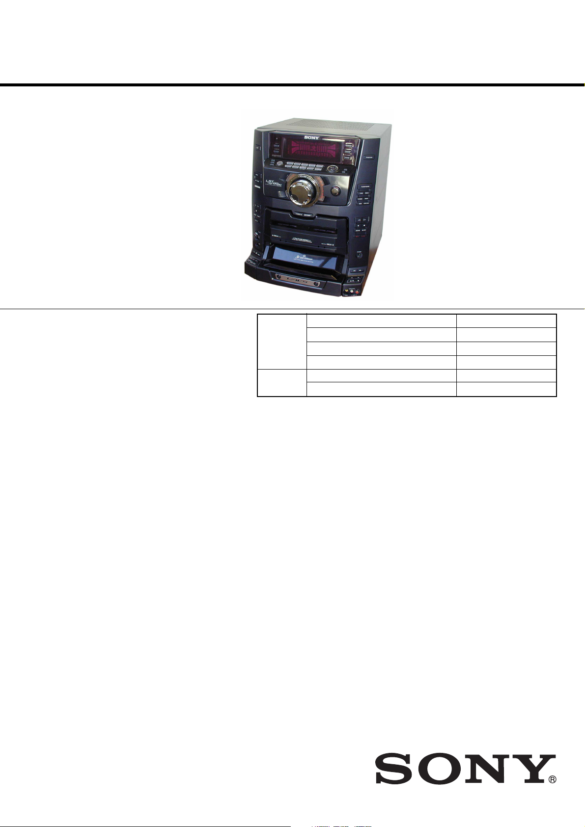
HCD-XGR99AV
SERVICE MANUAL
Ver. 1.1 2005.02
• HCD-XGR99AV is the Amplifier,
CD player, tape deck and tuner
section in LBT-XGR99AV.
Model Name Using Similar Mechanism HCD-XGR90AV
CD CD Mechanism Type CDM37B-30BD60C
Section Base Unit Name BU-30BD60C
Optical Pick-up Name A-MAX.3
TAPE Model Name Using Similar Mechanism NEW
Section Tape Mechanism Type CWM43RR23
Australian Model
SPECIFICATIONS
Amplifier section
Front speaker:
The following measured at AC 240 V 60 Hz
DIN power output (rated): 150 + 150 watts
(6 ohms at 1 kHz, DIN)
Continuous RMS power output (reference):
200 + 200 watts
(6 ohms at 1 kHz, 10% THD)
Center speaker:
DIN power output (rated): 35 watts
(8 ohms at 1 kHz, DIN)
Continuous RMS power output (reference):
50 watts
(8 ohms at 1 kHz, 10% THD)
Surround speaker:
DIN power output (rated): 35 + 35 watts
(8 ohms at 1 kHz, DIN)
Continuous RMS power output (reference):
50 + 50 watts
(8 ohms at 1 kHz, 10% THD)
Inputs
PHONO IN (phono jacks): sensitivity 3 mV, impedance 47 kilohms
MIC1/2 (phone jacks): sensitivity 1 mV, impedance 10 kilohms
GAME INPUT AUDIO (phono jacks):
sensitivity 250 mV, impedance 47 kilohms
GAME INPUT VIDEO (phono jack):
1Vp-p, 75 ohms
MD (VIDEO) IN (phono jacks): sensitivity 450 mV (250 mV),
impedance 47 kilohms
DVD INPUT
FRONT, REAR, CENTER, WOOFER (phono jacks):
sensitivity 450 mV, impedance 47 kilohms
DVD VIDEO INPUT (phono jack):
1Vp-p, 75 ohms
Outputs
PHONES (stereo phone jack): accepts headphones of 8 ohms or more
MD (VIDEO) OUT (phono jacks):
voltage 250 mV, impedance 1 kilohms
VIDEO OUT (phono jack): max. output level 1Vp-p,
load impedance 75 ohms
SUB WOOFER OUT (phono jack):
voltage 1 V, impedance 1 kilohm
FRONT SPEAKER: accepts impedance of 6 to 16 ohms
CENTER SPEAKER: accepts impedance of 8 to 16 ohms
SURROUND SPEAKER: accepts impedance of 8 to 16 ohms
— Continued on next page —
9-877-284-02
2005B02-1
© 2005.02
COMPONENT Hi-Fi STEREO SYSTEM
Sony Corporation
Audio Group
Published by Sony Engineering Corporation
HCD-XGR99AV
CD player section
System Compact disc digital audio system
Laser Semiconductor laser (λ=795 nm)
Emission duration: continuous
Frequency response 2 Hz – 20 kHz (±0.5 dB)
Signal-to-noise ratio More than 90 dB
Dynamic range More than 90 dB
CD OPTICAL DIGITAL OUT
(square optical connector jack, rear panel)
Wavelength 660 nm
Output level –18 dBm
Tape deck section
Recording system 4-track 2-channel, stereo
Frequency response 50 – 13,000 Hz (±3 dB),
using Sony TYPE I cassettes
Tuner section
FM stereo, FM/AM superheterodyne tuner
FM tuner section
Tuning range: 87.5 – 108.0 MHz (50 kHz step)
Antenna FM lead antenna
Antenna terminals 75 ohms unbalanced
Intermediate frequency 10.7 MHz
AM tuner section
Tuning range: 530 – 1,710 kHz
(with the tuning interval set at 10 kHz)
531 – 1,602 kHz
(with the tuning interval set at 9 kHz)
Antenna AM loop antenna
Antenna terminals External antenna terminal
Intermediate frequency 450 kHz
Notes on chip component replacement
• Never reuse a disconnected chip component.
• Notice that the minus side of a tantalum capacitor may be
damaged by heat.
Flexible Circuit Board Repairing
• Keep the temperature of soldering iron around 270˚C
during repairing.
• Do not touch the soldering iron on the same conductor of the
circuit board (within 3 times).
• Be careful not to apply force on the conductor when soldering
or unsoldering.
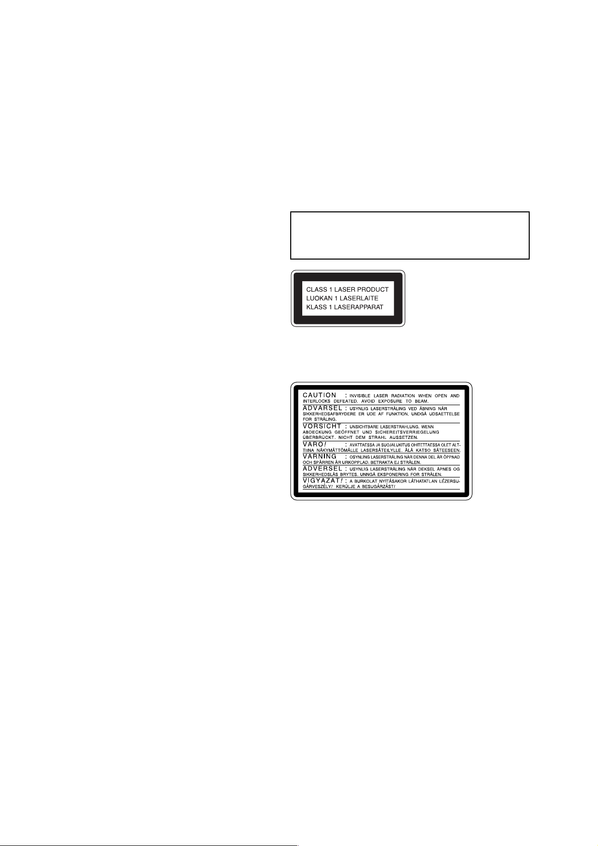
CAUTION
Use of controls or adjustments or performance of procedures
other than those specified herein may result in hazardous radiation
exposure.
This appliance is classified as a CLASS 1 LASER product. The
CLASS 1 LASER PRODUCT MARKING is located on the rear
exterior.
General
Power requirements 230 – 240 V AC, 50/60 Hz
Power consumption 230 watts
Dimensions (w/h/d) Approx. 355 x 425 x 451 mm
Mass Approx. 15.4 kg
Supplied accessories: AM loop antenna (1)
FM lead antenna (1)
Speaker cords (5)
Speaker pads (12)
Remote Commander (1)
Batteries (2)
Design and specifications are subject to change without notice.
SAFETY-RELATED COMPONENT WARNING!!
COMPONENTS IDENTIFIED BY MARK 0 OR DOTTED LINE WITH
MARK 0 ON THE SCHEMATIC DIAGRAMS AND IN THE PARTS
LIST ARE CRITICAL TO SAFE OPERATION. REPLACE THESE
COMPONENTS WITH SONY PARTS WHOSE PART NUMBERS
APPEAR AS SHOWN IN THIS MANUAL OR IN SUPPLEMENTS
PUBLISHED BY SONY .
2

HCD-XGR99AV
NOTES ON HANDLING THE OPTICAL PICK-UP
BLOCK OR BASE UNIT
The laser diode in the optical pick-up block may suffer electrostatic
break-down because of the potential difference generated by the
charged electrostatic load, etc. on clothing and the human body.
During repair, pay attention to electrostatic break-down and also
use the procedure in the printed matter which is included in the
repair parts.
The flexible board is easily damaged and should be handled with
care.
NOTES ON LASER DIODE EMISSION CHECK
The laser beam on this model is concentrated so as to be focused on
the disc reflective surface by the objective lens in the optical pickup block. Therefore, when checking the laser diode emission,
observe from more than 30 cm away from the objective lens.
LASER DIODE AND FOCUS SEARCH OPERATION
CHECK
Carry out the “S curve check” in “CD section adjustment” and
check that the S curve waveforms is output three times.
TABLE OF CONTENTS
1. SERVICING NOTE·························································· 4
2. GENERAL ·········································································· 5
3. DISASSEMBY···································································7
4. TEST MODE ···································································· 16
5. MECHANICAL ADJUSTMENTS ····························· 18
6. ELECTRICAL ADJUSTMENTS ······························· 18
7. DIAGRAMS
7-1. Circuit Board Location ······················································ 21
7-2. Block Diagram – CD Servo Section – ······························· 22
Block Diagram – Tuner/Tape Deck Section – ··················· 23
Block Diagram – Main Section – ······································ 24
Block Diagram
– Display/Key Control/Power Supply Section –·········· 25
7-3. Printed Wiring Board – BD Section – ······························· 26
7-4. Schematic Diagram – BD Section – ·································· 27
7-5. Printed Wiring Board – Motor LED Section – ·················· 28
7-6. Schematic Diagram –Motor LED Section – ······················ 28
7-7. Schematic Diagram – Main (1/4) Section – ······················ 29
7-8. Schematic Diagram – Main (2/4) Section – ······················ 30
7-9. Schematic Diagram – Main (3/4) Section – ······················ 31
7-10.Schematic Diagram – Main (4/4) Section – ······················ 32
7-11.Printed W iring Board – Main Section – ····························· 33
7-12.Printed Wiring Board – CD-L, CD-R Section – ················34
7-13.Schematic Diagram – CD-L, CD-R Section –··················· 35
7-14.Printed Wiring Board – TC-A, TC-B Section – ················ 36
7-15.Schematic Diagram – TC-A, TC-B Section – ··················· 37
7-16.Printed Wiring Board – Panel VR, Key Section – ············· 38
7-17.Schematic Diagram – Panel VR, Key Section –················ 39
7-18.Printed Wiring Board – Panel FL Section –······················· 40
7-19.Schematic Diagram – Panel FL Section – ·························41
7-20.Printed Wiring Board – Power Amp Section – ··················42
7-21.Schematic Diagram – Power Amp Section –····················· 43
7-22. Printed Wiring Board – Sub Amp Section – ····················· 44
7-23.Schematic Diagram – Sub Amp Section –························· 45
7-24. Printed Wiring Board – Prologic Section –······················· 46
7-25.Schematic Diagram – Prologic Section – ·························· 47
7-26. Printed Wiring Board – Mic Section –······························ 48
7-27.Schematic Diagram – Mic Section – ································· 48
7-28. Printed Wiring Board – Power Supply Section –·············· 49
7-29.Schematic Diagram – Power Supply Section – ················· 49
7-30. IC Pin Function Description ············································· 50
7-31. IC Block Diagram ····························································· 55
8. EXPLODED VIEWS
8-1. Case,Back Panel Section ··················································· 58
8-2. Front Panel Section-1 ························································ 59
8-3. Front Panel Section-2 ························································ 60
8-4. Chassis Section ·································································· 61
8-5. CD Mechanism Deck Section
(CDM-30BD60C)······························································· 62
8-6. Base Unit Section (BU-30BD60C)···································· 63
9. ELECTRICAL PARTS LIST ······································· 64
3
HCD-XGR99AV
SECTION 1
SERVICING NOTE
JIG FOR CHECKING PROLOGIC BOARD
The special jig (J-2501-216-A) is useful for checking the PROLOGIC board.
CN201
PROLOGIC board
MAIN board
CN202
Jig (J-2501-216-A)
CN151
SERVICE POSITION FOR BD BOARD AND OPTICAL PICK-UP BLOCK
CN152
3
Bottom plate
1
4
BD board
2
4
BU fitting screw
Two screws (+BVTP 3 x 8)
5
Optical pick-up block
SECTION 2
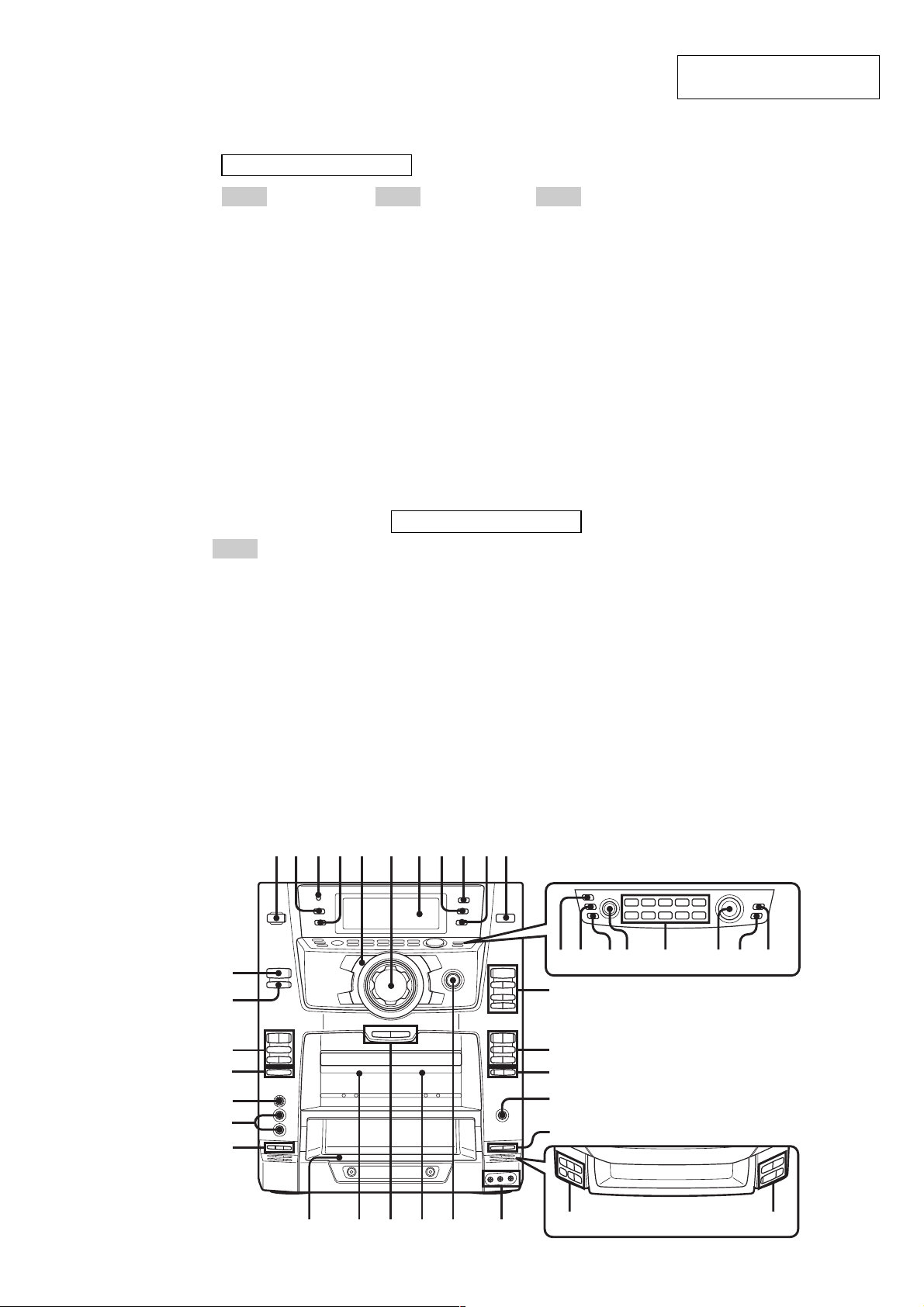
GENERAL
Main unit
ALPHABETICAL ORDER
A – E F – O P – R
CD SYNC qf
Deck A wa
Deck B ql
DIRECTION wh
DISC 1 – 5 ek
DISC SKIP ek
Disc tray ws
DISPLAY 2
Display window 7
DVD 5.1CH e;
EDIT wd
EFFECT ej
ENTER eg
FM MODE qs
FUNCTION qa
GAME wl
GAME INPUT
AUDIO L/R jacks
GAME INPUT
VIDEO jack qj
GAME MIXING wk
ILLUMINATION 4
MEMORY qs
MIC1/MIC2 jacks wf
MIC LEVEL wg
qj
PARTY ed
PARTY MODE ef
P FILE eh
PHONES jack qg
PLAY MODE wd
Power illuminator 5
PRESET EQ ef
PRO LOGIC es
PUSH OPEN ws
Remote sensor 3
REPEAT wd
HCD-XGR99AV
This section is extracted from
instruction manual.
SAMBA/ROCK/DISCO/
BALLAD/TECHNO
SALSA/REGGAE/TANGO/
MOVIE/GAME
S – Z
SLEEP 9
SURROUND ea
TIMER SELECT 8
TUNER ENTER qs
TUNER/BAND qs
TUNING +/– qs
TUNING MODE qs
VOLUME control 6
X-GROOVE qk
23 745 8690qa1
wl
wk
BUTTON DESCRIPTIONS
?/1 (power) 1
c/CLOCK SET 0
z REC qf
x (stop) el
m/M (rewind/fast forward)
NX (play/pause) el
h/H (play) qd wj
x (stop) qd wj
X (pause) qd
.m/M> (rewind/fast
forward) qd wj
./> (go back/go forward)
M/m/</, eg
A EJECTZ/Z B EJECT (eject )
e; es
qs
el
qh
w;
ed ef egeh ejea
wj
wh
wg
wf
wd
qd
qf
qg
qh
qjqkw; qlwaws
elek
5
HCD-XGR99AV
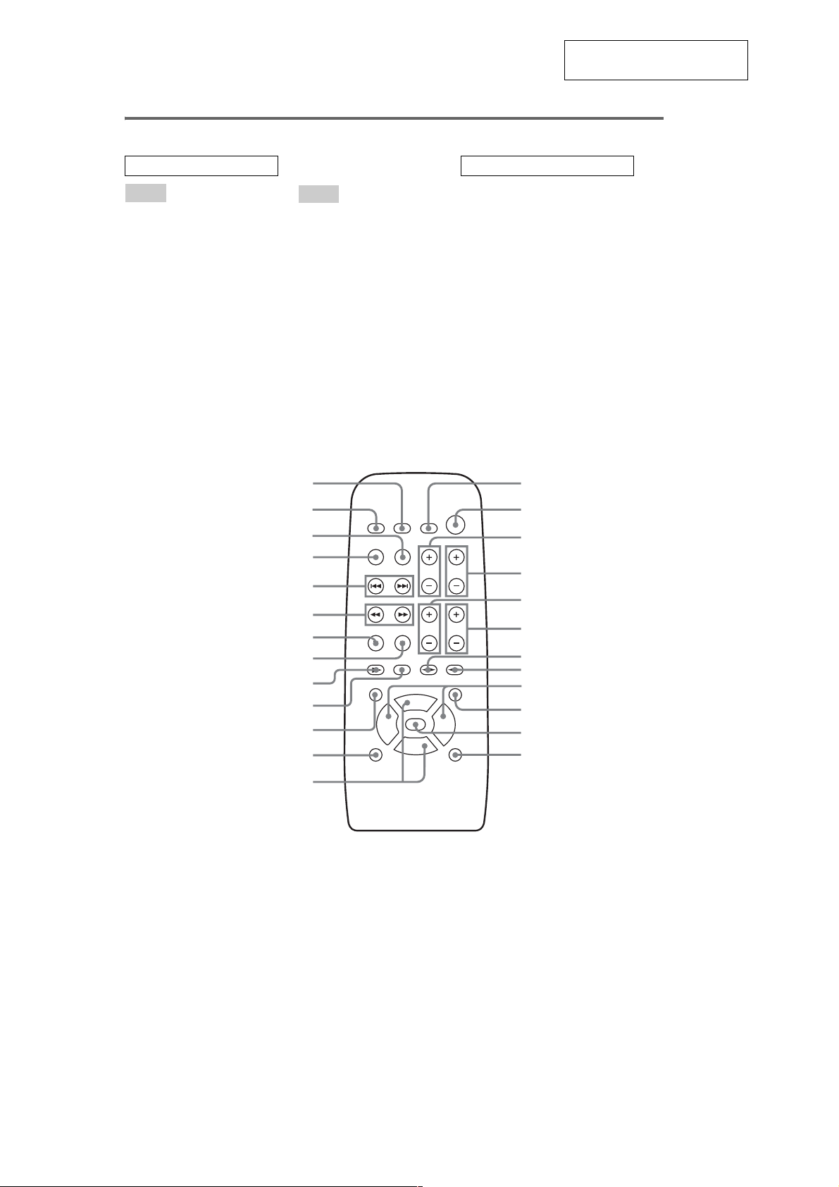
Remote control
This section is extracted from
instruction manual.
ALPHABETICAL ORDER
A – P
CENTER LEVEL +/– 5
CLEAR wd
DISC SKIP ws
EFFECT qa
FILE SELECT +/– 9
FUNCTION q;
PRESET +/– wa
PRO LOGIC qg
Q – Z
SLEEP wf
SURR qs
SURR LEVEL +/– 6
TEST TONE qf
TUNER/BAND qh
TUNING +/– w;
TV CH +/– 4
TV/VIDEO wg
TV VOL +/– 3
VOL +/– qd
wg
wf
wd
ws
wa
w;
ql
qk
qj
qh
qg
qf
BUTTON DESCRIPTIONS
?/1 (power) 2
m/M (rewind/fast forward)
./> (go back/go forward)
X (pause) ql
x (stop) qk
CD N (play) qj
TAPE AnN (play) 7
TAPE BnN (play) 8
TV ?/1 (power) 1
1
2
3
4
5
6
7
8
9
q;
qa
qs
w;
wa
qd
6
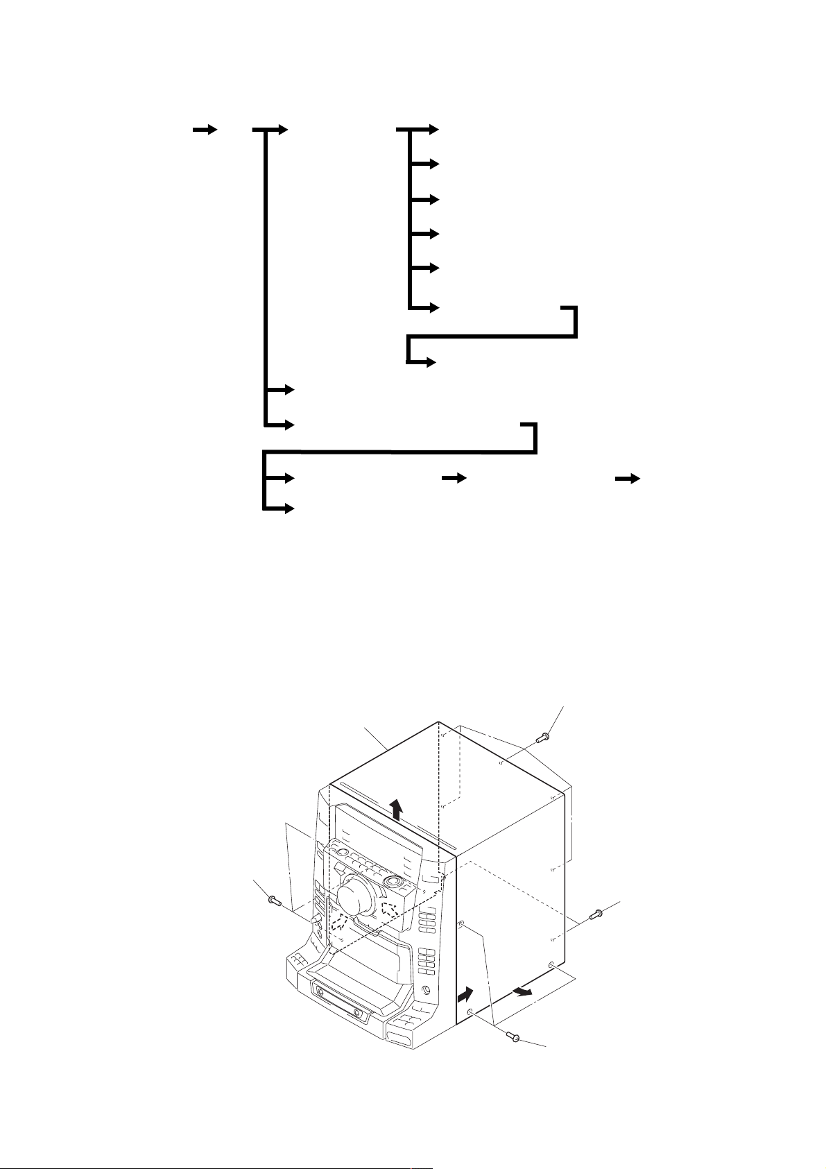
SECTION 3
DISASSEMBLY
• The equipment can be removed using the following procedure.
Set Case Front panel section Tape mechanism deck
Back panel, DC fan, MAIN board, PROLOGIC board
CD mechanism deck (CDM37B-30BD60C)
HCD-XGR99AV
PANEL FL board, GAME board, TC-A board,
TUNER board, TC-B board
KEY board
PANEL VR board
HEADPHONE board, MIC VR board, MIC board
FRONT INPUT board
CD-L board, D-SW board, CD-R board
Base unit-1 (BU-30BD60C)
Disc table
Note : Follow the disassembly procedure in the numerical order given.
3-1. CASE
8
Case
7
1
Three screws (CASE3 TP2)
Base unit-2 (BU-30BD60C) BD board
3
Five screws (BVTT 3x6)
6
4
Two screws (BVTP 3x8)
5
2
Three screws (CASE3 TP2)
7
HCD-XGR99AV
)
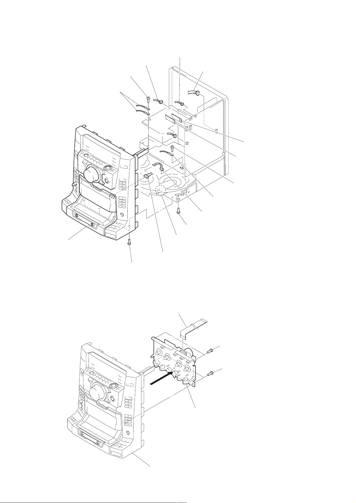
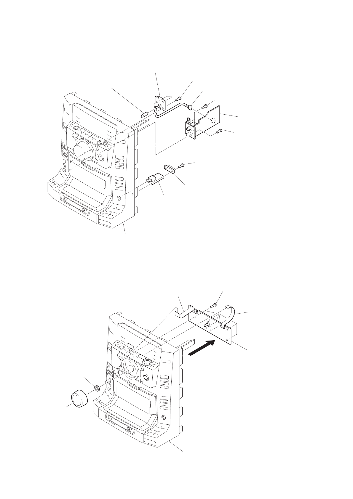
3-2. FRONT PANEL SECTION
7
Screw (BVTP 3x8)
8
3
Connector (CN311)
Lugs
4
Connector (CN903)
5
Connector (CN722)
1
Flat type wire (CN371
2
Flat type wire (CN431)
9
Screw (BVTP 3x8)
qg
Front panel section
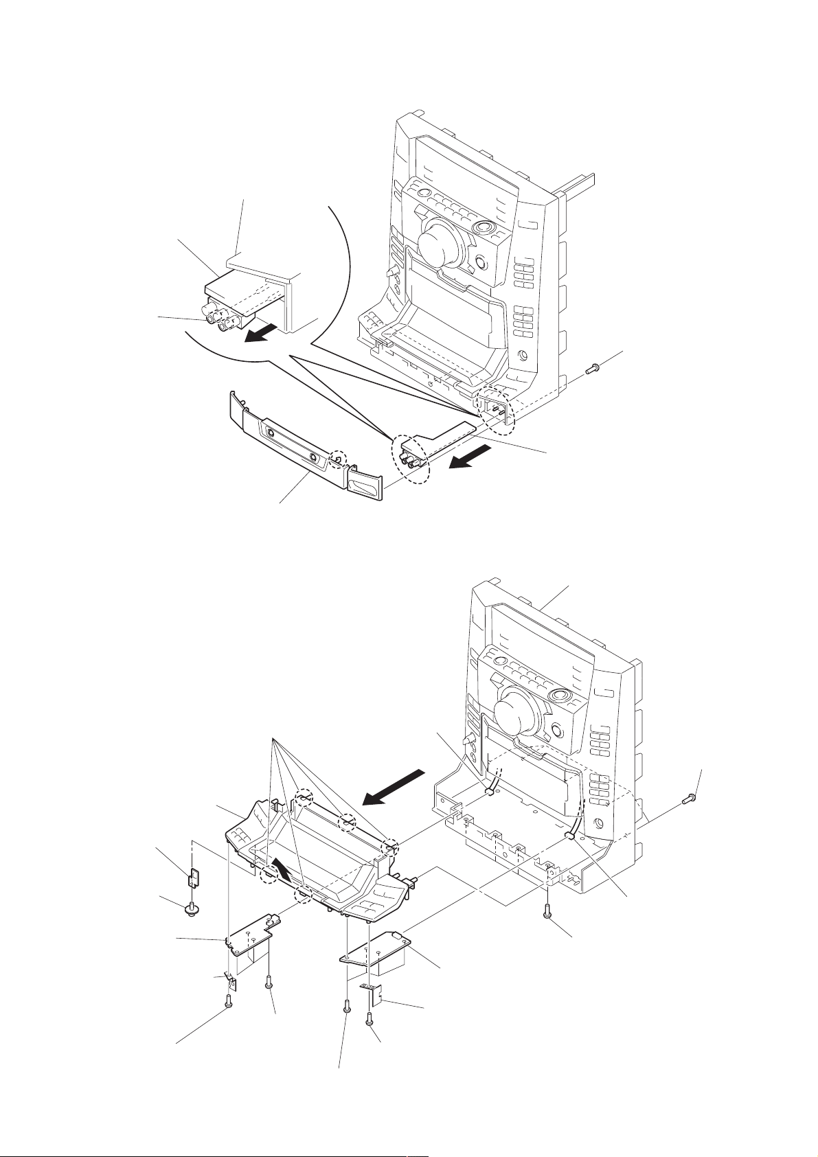
3-3. TAPE MECHANISM DECK
qa
Connector (B deck)
qd
Four screws (BVTP 3x8)
1
Flat type wire (13 core)
4
qs
Screw (BVTP 3x8)
qf
Claw
0
Lug
6
Connector (CN806)
2
Two screws (BVTP 2.6x8)
3
Two screws (BVTP 2.6x8)
5
Tape mechanism deck
Front panel
8
3-4. PANEL FL BOARD, GAME BOARD, TC-A BOARD, TUNER BOARD, TC-B BOARD
)
Five screws (BVTP 2.6x8)
qa
7
(CN601)
qf
2
Bracket (TA)
ql
Two claws
1
Screw (BVTP 2.6x8)
qh Two
w;
claws
GAME board
ws
TC-A board
qs
Four screws
(BVTP 2.6x8)
5
(CN700)
qk
board
qj
qd
Four screws
(BVTP 2.6x8)
Connector
wd
Three claws
PANEL FL
HCD-XGR99AV
Flat type wire
8
Screw (BVTP 2.6x8)
9
Bracket (MAIN)
0
Four screws (BVTP 2.6x8)
Four screws (BVTP 2.6x8)
wf
TUNER board
qg
Four screws
(BVTP 2.6x8)
wa
Three claws
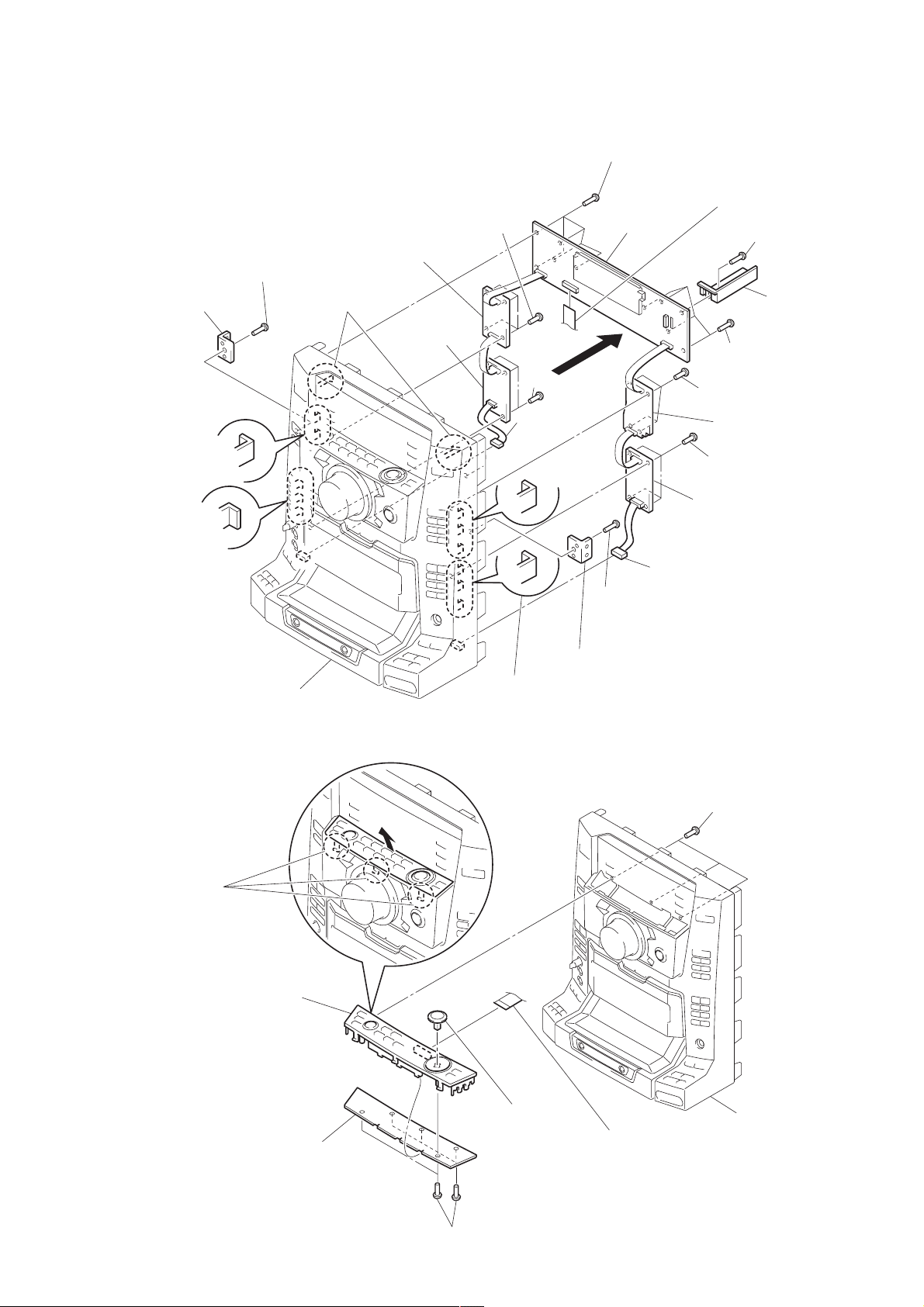
3-5. KEY BOARD
6
Three claws
Front panel
7
wg
Three claws
3
Screw (BVTP 2.6x8)
4
Bracket (TA)
wh
TC-B board
6
Connector (CN600)
1
Three screws (BVTP 2.6x8
2
OPERATION PANEL ASSY
8
KEY board
4
Cursor
5
Five screws (BVTP 2.6x8)
3
Flat type wire (CN801)
Front panel
9
HCD-XGR99AV
)
)
3-6. HEADPHONE BOARD, MIC VR BOARD, MIC BOARD
7
MIC VR board
6
Knob (MIC)
5
Three screws (BVTP 2.6x8)
4
Connector (CN812)
8
Two screws (BVTP 2.6x8)
1 S
crew (BVTP 2.6x8)
2
0
MIC board
9 S
crew (BVTP 2.6x8
3-7. PANEL VR BOARD
Front panel
3
HEADPHONE board
3
Flat type wire (CN601)
6
5
Six screws (BVTP 2.6x8)
4
Flat type wire (CN801
7
PANEL VR board
10
2
Nut (Supplied with S700)
1
Volume knob
Front panel
1
Five screws (BVTP 2.6x8)
4
FRONT INPUT board
2
Bumper ASSY
J500
FRONT INPUT board
Front panel
3
)
3-8. FRONT INPUT BOARD
HCD-XGR99AV
3-9. CD-L BOARD, DOOR SW BOARD, CD-R BOARD
qd
Froating screw
(DIA.12)
8
Sub panel CD ASSY
qf
DOOR SW
board
qs
CD-L board
0
BRACKET (S/P) (L)
5
Five claws
6
3
Connector (CN700)
7
qk
CD-R board
Front panel
2
Four screws (BVTP 2.6x8)
1
Five screws (BVTP 2.6x8
4
Connector (CN600)
9
Screw (BVTP 2.6x8)
qa
Four screws
(BVTP 2.6x8)
qj
Four screws (BVTP 2.6x8)
qh
qg
Screw (BVTP 2.6x8)
BRACKET (S/P) (R)
11
HCD-XGR99AV
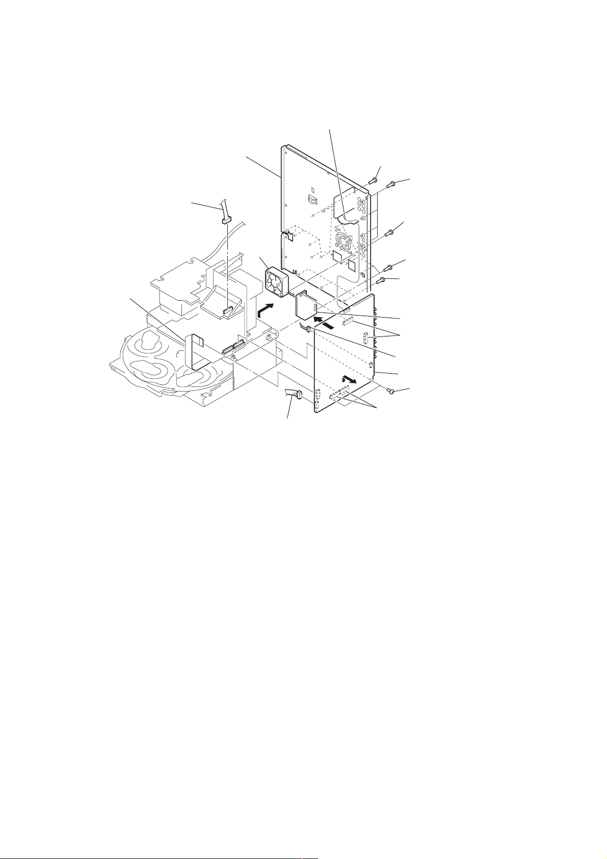
3-10. BACK PANEL, DC FAN, MAIN BOARD, PROLOGIC BOARD
1
Flat type wire (CN441)
7
Back panel
qd
Connector (CN102)
0
DC FAN
(M901)
qa
Flat type wire
(CN401)
6
qs
Connector (CN411)
2
Eight screws
(BVTP 3 X 8)
qk
3
Four screws
(BVTP 3 X 8)
9
Two screws
(BVTP 3 X 8)
5
Five screws
(BVTP 3 X 8)
4
Three screws
(BVTP 3 X 8)
ql
PROLOGIC board
qj
Two connectors
(CN151, 152)
8
Connector (CN961)
qh
MAIN board
qf
Two screws
(BVTP 3 X 8)
qg
Two connectors
(CN901, 902)
12
m
3-11. CD MECHANISM DECK (CDM37B-30BD60C)
1
Flat type wire
(CN401)
4
Three screws
(BVTP 3 X 8)
7
2
Connector
(CN411)
6
Two screws (BVTP 3 X 8)
8
7
HCD-XGR99AV
3
Four screws (BVTP 3 X 8)
Wire holder
5
Two screws
(BVTP 3 X 8)
qa
CD mechanism deck
(CDM37B-30BD60C)
0
Five screws
(BVTP3 × 8)
9
Remove two cables fro
wire holder.
13
HCD-XGR99AV
)
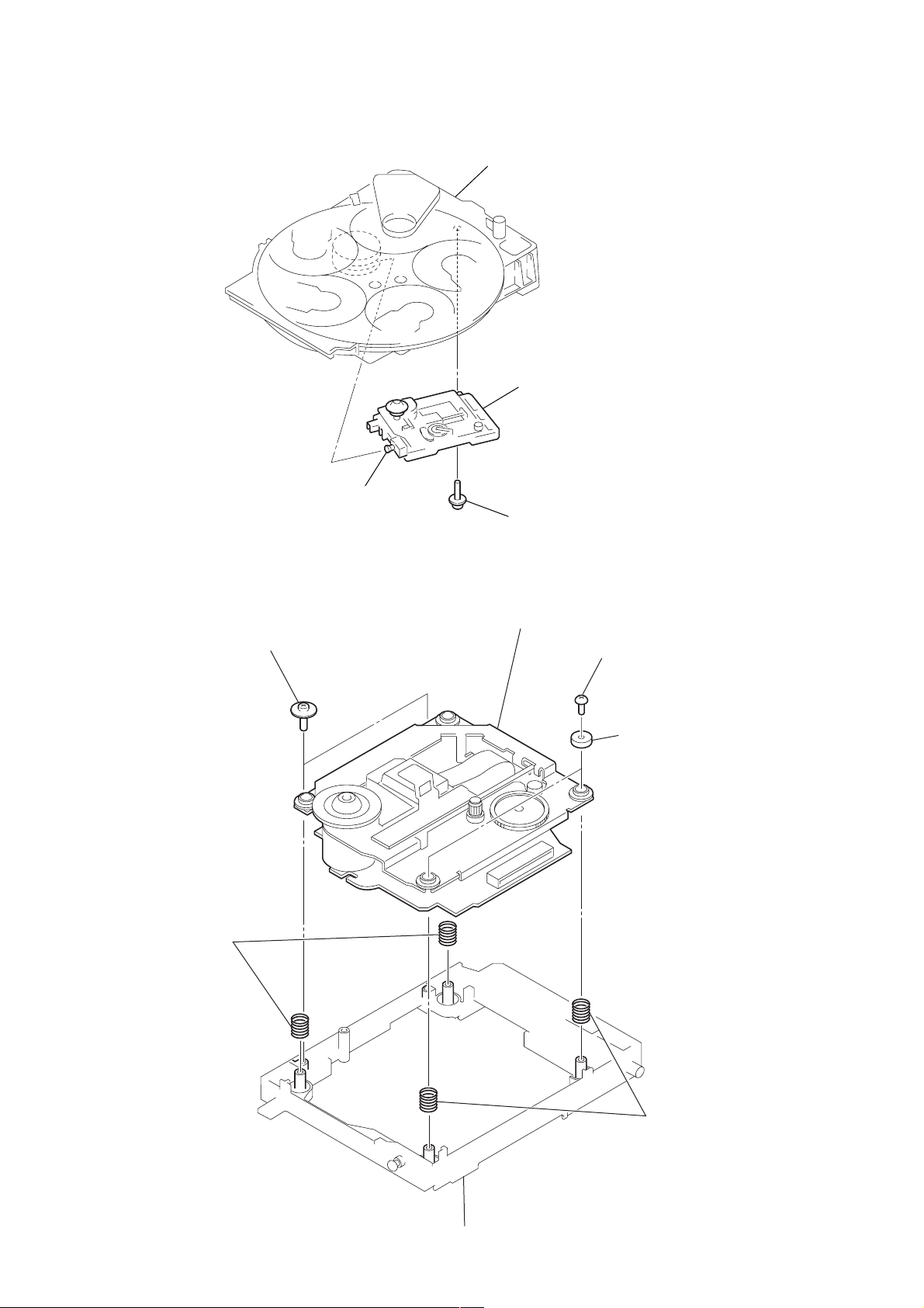
3-12. BASE UNIT-1 (BU-30BD60C)
CD mechanism deck
(CDM37B-30BD60C)
3
Base unit
(BU-30BD60C)
3-13. BASE UNIT-2 (BU-30BD60C)
1
Two floating screws (DIA.12)
4
Two coil springs
(insulator)
2
Boss
1
BU fitting screw
6
Base unit (BU-30BD60C)
2
Two screws
(BVTP 2.6 X 8)
3
Two stoppers
(BU)
14
Holder (BU30) assy
5
Two coil
springs
(insulator
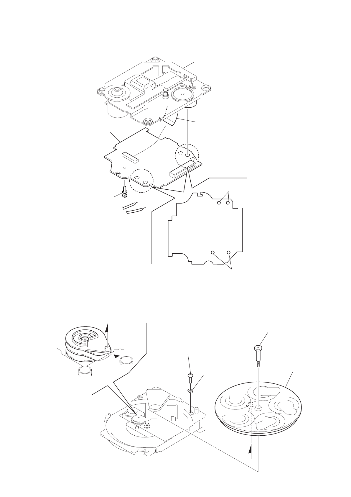
3-14. BD BOARD
e
5
BD board
BU-30BD60C
4
Flat type wire (CN102)
HCD-XGR99AV
3
Rivet
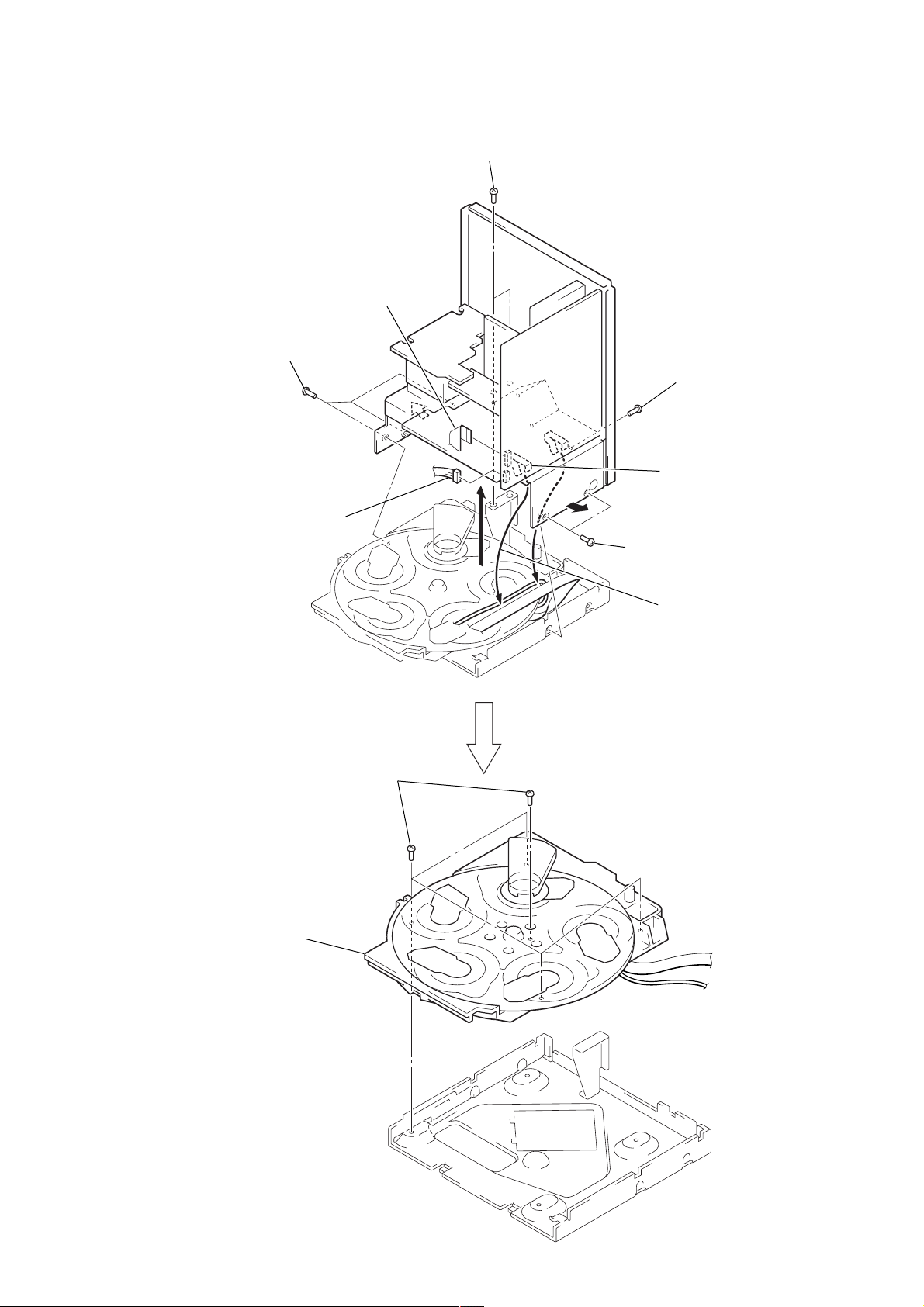
3-15. DISC TABLE
Note: When the disc table is installed, adjust the positions of roller cam
and mark B as shown in the figure, then set to the groove of disc
table.
A
1
Screw (BVTP 3
1
Remove the two solders.
2
Remove the two solders.
×
8)
3
Step screw
2
Bracket (BU)
4
Disc tabl
A
15
HCD-XGR99AV
B
SECTION 4
TEST MODE
[MC Cold Reset]
• The cold reset clears all data including preset data stored in the
RAM to initial conditions. Execute this mode when returning
the set to the customer.
Procedure:
1. Turn the power ON or set to the DEMO mode.
2. Press three buttons of x (TC-B) , TUNER ENTER , and \/1
simultaneously.
3. The set is reset, and displays “COLD RESET”, then becomes
DEMO mode.
[Change-over the AM Tuning Interval]
• The AM tuning interval can be changed over 9 kHz or 10 kHz.
Procedure:
1. Press the \/1 button to turn the power ON.
2. Select the function “TUNER”, and press the TUNER/BAND
button to select the BAND “AM”.
3. Press the \/1 button to turn the power OFF.
4. Press the ENTER and \/1 buttons simultaneously,
and the display on the fluorescent indicator tube changes to
“AM 9 K STEP” or “AM 10 K STEP”, and thus the tuning
interval is changed over.
[CD Ship Mode] (No memory clear)
• This mode moves the optical pick-up to the position durable to
vibration. Use this mode when returning the set to the customer
after repair.
Procedure:
1. Press the \/1 button to turn the power ON.
2. Press the EDIT and
3. A message “LOCK” is displayed on the fluorescent indicator
tube, and the CD delivery mode is set.
[LED and Fluorescent Indicator Tube All Lit, Key Check
Mode]
Procedure:
1. Press three buttons of x (TC-B) , TUNER ENTER ,and
DISC 2 simultaneously.
2. LEDs and fluorescent indicator tube are all turned on.
3. Press the DISC 1 button, the MODE and DESTINATION are
displayed fluorescent indicator tube.
4. Each time the DISC 1 button is pressed, the MC/GC category
version is displayed in the following order.
5. Press the DISC 2 button, and the key check mode is acti-vated.
NR MC GC CD CDDM CDMA
6. In the key check mode, the fluorescent indicator tube displays
“K 0 J0 V0”. Each time a button is pressed, “K” value in-creases
to “K69”call the button is pressed.However, once a button is
pressed, it is no longer taken into account.
“V” value increases like 1, 2, 3 ... if turn the VOLUME dial
clockwise (“+” direction), or it decreases like 0, 9, 8 ... if turn
the VOLUME dial counterclockwise (“–” direction).
7. To release from this mode, press three buttons in the same
manner as step 1, or disconnect the power cord.
buttons simultaneously.
\/1
BDABDBSTTATMTC
CDM
[Sled Servo Mode] (CD service mode)
• This mode can run the CD sled motor freely. Use this mode, for
instance, when cleaning the pick-up.
Procedure:
1. Select the function “CD”.
2. Press three buttons x (TC-B) , TUNER ENTER , and
DISC 5 simultaneously.
3. The Sled Servo mode is selected, if “CD” is blanking on the
fluorescent indicator tube.
4. With the CD in stop status, press M button in CD section to
move the pick-up to outside track, or m button to inside track.
5. To exit from this mode, press
OFF.
Note:
• Always move the pick-up to most inside track when exiting from
this mode. Otherwise, a disc will not be unloaded.
• Do not run the sled motor excessively, otherwise the gear can
be chipped.
[Change-over of FUNCTION Name]
• The FUNCTION name of external input terminal can be changed
over to VIDEO or MD. W ith the FUNCTION selected to “MD”,
about 5dB mute is applied to the input gain.
Procedure:
1. Press \/1 button to turn the power OFF.
2. Press
several seconds, and the power is turned on, the display of
fluorescent indicator tube changes to “MD” or “VIDEO”
instantaneously, and thus the FUNCTION is changed over.
[Aging Mode]
This mode can be used for operation check of tape deck section.
Tape deck section work in parallel.
• If an error occurred:
The aging operation stops and display then status.
• If no error occurs:
The aging operation continues repeatedly.
Procedure:
1. Load the tapes into the decks A and B respectively.
2. Press the FUNCTION button to select the function “CD”.
3. Press the PLAY MODE button to set the “ALL DISCS” mode,
and press the REPEAT button to “REPEAT” off.
4. Press three buttons of x (TC-B) , TUNER ENTER ,and
DISC 4 simultaneously.
5. The aging mode is activated, if the indicator of disc tray number on the fluorescent indicator tube is blinking.
6. To release from the aging mode, press the \/1 button to turn
the power OFF and operate the cold reset. (Refer to the “MC
Cold Reset”)
1. Display at the Aging Mode
• Display operating state of tape deck section alternately.
• If an error occurred, stop display.
button together with FUNCTION button for
\/1
button turn to the power
\/1
16
HCD-XGR99AV
2. Tape Deck Section
• The sequence during the aging mode is following as below.
• If an error occurred, stop display that step.
Aging mode sequence (Tape deck section):
Rewind the tape A
“T APE A AG-1”
Shut off
FWD the tape A
“T APE A AG-2”
2 minutes
Fast forward the tape A
“T APE A AG-3”
Shut off or 20 seconds
RVS the tape A
“T APE A AG-4”
2 minutes
Rewind the tape A
“T APE A AG-5”
Shut off
3. CD Section
• The sequence during the aging mode is following as below.
• If an error occurred, stop display that step.
Aging mode sequence (CD section):
Tray T urn
DISC 1
chucking
TOC Read
Track 1 Play
2 seconds
Last Track Play
2 seconds
FWD the tape B
“TAPE B AG-2”
2 minutes
Fast forward the tape B
“TAPE B AG-3”
Shut off or 20 seconds
RVS the tape B
“TAPE B AG-4”
2 minutes
Rewind the tape B
“TAPE B AG-5”
Shut off
Note: “TAPE * AG- * ” is display of each step.
Tray Tun
DISC 4
Chucking
TOC Read
Track 1 Play
2 seconds
Last Track play
[VACS ON/OFF]
• The volume control by VACS is turned ON/OFF.
Procedure:
1. Press the \/1 button to turn the power ON.
2. Press the PLAY MODE and \/1 buttons simultaneously.
3. The reaction display appears when switcing ON/OFF.
17
HCD-XGR99AV
SECTION 5
MECHANICAL ADJUSTMENTS
Precaution
1. Clean the following parts with a denatured alcohol-moistened
swab:
record/playback heads pinch rollers
erase head rubber belts
capstan idlers
2. Demagnetize the record/playback head with a head demagnetizer.
3. Do not use a magnetized screwdriver for the adjustments.
4. After the adjustments, apply suitable locking compound to the
parts adjusted.
5. The adjustments should be performed with the rated power supply voltage unless otherwise noted.
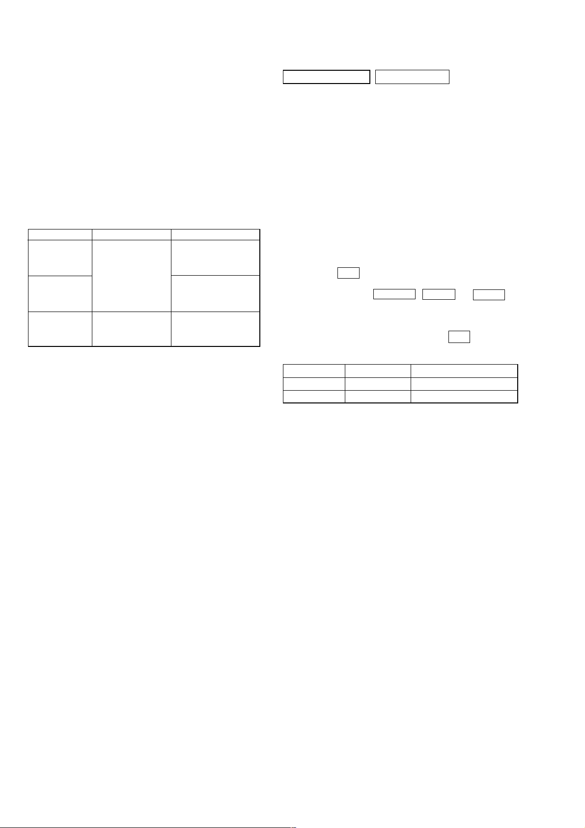
Torque Measurement
Mode Torque Meter Meter Reading
2.9~6.9 mN•m
FWD (30 to 70 g•cm)
CQ-102C
FWD
back tension (2 to 6 g•cm)
FF/REW CQ-201B (80 to 170 g•cm)
(0.42 – 0.97 oz•inch)
0.19~0.59 mN•m
(0.03 – 0.08 oz•inch)
7.8~16.7 mN•m
(1.11 – 2.36 oz • inch)
SECTION 6
ELECTRICAL ADJUSTMENTS
DECK SECTION 0 dB = 0.775 V
Precaution
1. Demagnetize the record/playback head with a head demagnetizer.
2. Do not use a magnetized screwdriver for the adjustments.
3. After the adjustments, apply suitable locking compound to the
parts adjust.
4. The adjustments should be performed with the rated power
supply voltage unless otherwise noted.
5. The adjustments should be performed in the order given in
this service manual. (As a general rule, playback circuit
adjustment should be completed before performing recording
circuit adjustment.)
6. The adjustments should be performed for both L-CH and R-CH.
7. Switches and controls should be set as follows unless otherwise specified.
8. Set to the DOLBY NR OFF.
9. Set to the test mode.
(1) Press the \/1 button to turn the power ON.
(2) Select the function “TAPE A or B”.
(3) Press the button of x (TC-B) , ENTER ,and DISC 3
simultaneously, to set the tape deck test mode
and displays “TEST MODE” on the fluorescent indicator
tube.
(4) To release from the test mode, press the \/1 button.
• Test Tape
Tape Signal Used for
P-4-A100 10 kHz, – 10 dB Azimuth Adjustment
WS-48B 3 kHz, 0 dB Tape Speed Adjustment
18
HCD-XGR99AV
)
forward
reverse
Record/Playback Head Azimuth Adjustment
DECK A DECK B
Note: Perform this adjustments for both decks
Procedure:
1. Mode: Playback (FWD)
test tape
P-4-A100
(10 kHz, – 10 dB)
MAIN board
MD (VIDEO) OUT jack (J701
L-CH, R-CH
level meter
set
+
2. Turn the adjustment screw and check output peaks. If the peaks
do not match for L-CH and R-CH, turn the adjustment screw
so that outputs match within 1dB of peak.
Output
level
within
1dB
within
1dB
L-CH
peak
Adjustment Location: Playback Head (Deck A).
Record/Playback/Erase Head (Deck B).
R-CH
Screw
position
peak
L-CH
peak
R-CH
peak
Screw
position
3. Mode: Playback
MAIN board
test tape
P-4-A100
(10 kHz, – 10 dB)
L-CH
set
R-CH
in phase 45°90°135°180
MD (VIDEO) OUT jack (J701)
L-CH
R-CH
waveform of oscilloscope
good
oscilloscope
wrong
H
V
°
4. Repeat step 1 to 3 in playback (REV) mode.
5. After the adjustments, apply suitable locking compound to the
pats adjusted.
19
HCD-XGR99AV
e
)
CD SECTION
Note :
1. CD Block is basically designed to operate without adjustment.
Therefore, check each item in order given.
2. Use LUV-P01 (4-999-032-01) unless otherwise indicated.
3. Use an oscilloscope with more than 10M impedance.
4. Clean the object lens by an applicator with neutral detergent
when the signal level is low than specified value with the
following checks.
S-Curve Check
Oscilloscope
BD board
TP(FE)
TP(DVC)
Procedure :
1. Connect oscilloscope to TP (FE).
2. Connect between TP (FE) and TP (DVC ( 1.65 V) by lead
wire.
3. Press the \/1 button to turn the power ON.
4. Load a disc (LUV -P01) and actuate the focus search. (In consequence of open and close the disc tray, actuate the focus search)
5. Confirm that the oscilloscope waveform (S-curve) is symmetrical between A and B. And confirm peak to peak level within 2
±0.5 Vp-p.
S-curve waveform
symmetry
A
±
within 4
B
1Vp-p
Note: Clear RF signal waveform means that the shape “◊” can be
clearly distinguished at the center of the waveform.
VOLT/DIV : 200mV
TIME/DIV : 500ns
±
level : 1.45
0.3Vp-p
E-F Balance (1 Track jump) Check
oscilloscop
BD board
TP(TE)
TP(DVC)
Procedure:
1. Connect oscilloscope to TP (TE) and TP (DVC) board.
2. Press the \/1 button to turn the power ON.
3. Load a disc (LUV-P01) and playback the number nine track.
4. Press the bB button. (Becomes the 1track jump mode.)
5. Confirm that the level B and A (DC voltage) on the oscilloscope waveform.
center of
waveform
B
0V
B=1.3 ± 0.6Vp-p
Specified level: × 100=less than – 22%
A
B
symmetry
A (DC voltage
6. After check, remove the lead wire connected in step 2.
Note : • Try to measure several times to make sure than the ratio
of A : B or B : A is more than 10 : 7.
• Take sweep time as long as possible and light up the
brightness to obtain best waveform.
RF Level Check
oscilloscope
BD board
TP(RFDC)
TP(RFAC)
Procedure :
1. Connect oscilloscope to TP2 (RFDC) and TP1 (RFAC).
2. Press the \/1 button to turn the power ON.
3. Load a disc (LUV-P01) and playback.
4. Confirm that oscilloscope waveform is clear and check RF
signal level is correct or not.
6. Adjust RV101 so that A (DC voltage) becomes 0.
Checking Location:
[BD BOARD]
DVC
RFAC
FE
SE
TE
RFDC
RV101
20
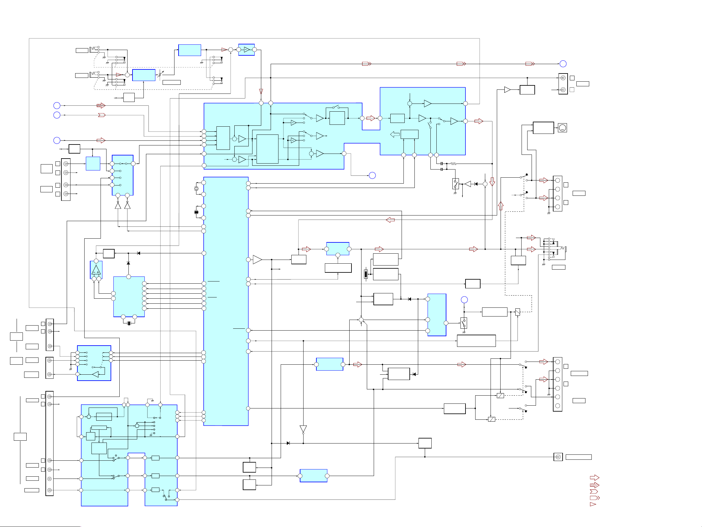
Five screws (BVTT 3x6)
7-1. CIRCUIT BOARD LOCATION
HCD-XGR99AV
SECTION 7
DIAGRAMS
GAME board
TC-A board
CD-L board
TRANS board
PANEL FL board
FRONT INPUT board
SUB TRANS board
TUNER PACK (FM/AM TUNER UNIT)
TC-B board
HEADPHONE board
CD-R board
SUB AMP board
PROLOGIC board
MAIN board
PA board
TUNER board
Note on Schematic Diagram:
• All capacitors are in µF unless otherwise noted. pF: µµF
50 WV or less are not indicated except for electrolytics
and tantalums.
• All resistors are in Ω and 1/
specified.
• f : internal component.
2
•
• 5 : fusible resistor.
• C : panel designation.
• A : B+ Line.
• B : B– Line.
• H : adjustment for repair.
•Voltages and waveforms are dc with respect to ground
•Voltages are taken with a VOM (Input impedance 10 MΩ).
•Waveforms are taken with a oscilloscope.
• Circled numbers refer to waveforms.
• Signal path.
: nonflammable resistor.
Note:
The components identified by mark 0 or dotted line
with mark 0 are critical for safety.
Replace only with part number specified.
under no-signal conditions.
BD board section
no mark: CD PLAY
Other board section
no mark: TUNER (FM/AM)
( ): TAPE PLAY
< >: TAPE REC
[ ]: CD PLAY
Voltage variations may be noted due to normal production tolerances.
Voltage variations may be noted due to normal production tolerances.
F : TUNER (FM/AM)
E : TAPE PALY (DECK A)
d : TAPE PALY (DECK B)
G : RECORD
J : CD PALY (ANALOG OUT)
c : CD PALY (DIGITAL OUT)
N : MIC INPUT
4
W or less unless otherwise
Note on Printed Wiring Boards:
• X : parts extracted from the component side.
• : Pattern from the side which enables seeing.
(The other layers´ Patterns are not indicated.)
• Indication of transistor.
C
B
B
B
Q
E
Q
CE
These are omitted.
These are omitted.
Q
CE
These are omitted.
KEY board
PANEL VR board
MIC board
MIC VR board
DOOR SW board
MOTOR board
SENSOR board
BD board
LED board
21
21
HCD-XGR99AV
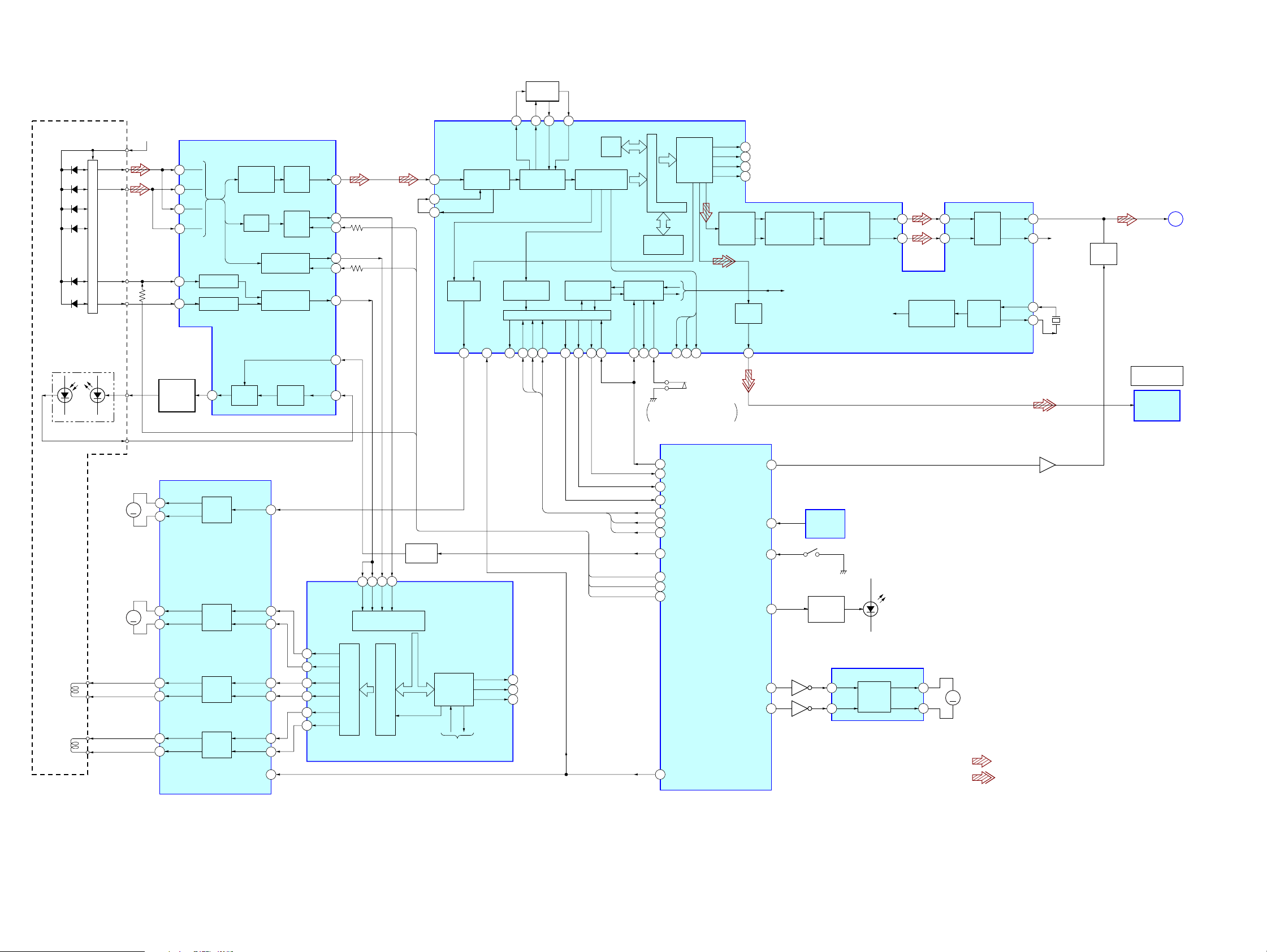
7-2. BLOCK DIAGRAMS
– CD SERVO SECTION –
CD D+5V
A
B
C
D
F
E
OPTICAL PICK-UP BLOCK
(A-MAX.3)
LASER DIODE
PD
I-V AMP
I5-10
LD
M101
SPINDLE
MOTOR
M102
SLED
MOTOR
PD1
PD2
I1-6
LD
PD
M
M
FOCUS/TRACKING ERROR AMP
A
6
B
7
C
8
D
9
F
11
F I-V AMP
E
10
E I-V AMP
LD
DRIVE
Q101
FOCUS/TRACKING COIL DRIVE,
SPINDLE/SLED MOTOR DRIVE
1
IC102
CH4OUTF
15
16
17
18
CH4OUTR
CH3OUTF
CH3OUTR
MOTOR
DRIVE
MOTOR
DRIVE
FILTER
RF AMP,
IC103
RF
SUMMING
AMP
∑
A-D
FOCUS
ERROR AMP
TRACKING
ERROR AMP
LD
APC LD
AMP
CH4SIN
CH3FIN
CH3RIN
APC PD
25
24
23
AMP
RF EQ
AMP
DC
AMP
RFAC
RFDCO
RFDCI
FEI
TE
SW
PD
15
28
29
FE
16
17
18
12
2
40
SE
43
39
41
FE
TE
RFDC
A/D
CONVERTER
PWM3
PWM1
PWM2
BUFFER
Q451-454
RFAC
51
ASYI
49
ASYO
48
DIGITAL
CLV
DIGITAL SERVO
PROCESSOR
IC101 (2/2)
ASYMMETRY
CORRECTION
MDP
26
3
XRST
SUBCODE
PROCESSOR
XLON
14 5 6
54 56
FILO
XLAT
DATA
X-LAT
CD-DATA
53
PCO
CLTV
DIGITAL
PLL
CPU INTERFACE
CLOK
7
CD-CLK
55
SENS
8
DIGITAL SIGNAL PROCESSOR,
DIGITAL FILTER, D/A CONVERTER
IC101 (1/2)
FILI
SERVO AUTO
EFM
DEMODULATOR
SEQUENCER
SQSO
SQCK
SCOR
20
1 2
16K
RAM
CD-DATA
INTERNAL BUS
ERROR
CORRECTOR
SERVO
INTERFACE
SSTP
SCLK
COUT
9 21
27
NCNC NC NC NC
When the optical pick-up
ON :
is inner position.
33
32
19
34
CD-CLK
37
X-LAT
36
35
40
PWM1
28
PWM2
26
PWM3
24
D/A
INTERFACE
EMPH
WFCK
64 15
(LIMIT)
SQ-CLK
SQ-DATA
SCOR
SENS
CD-CLK
XLT
CD-DATA
HOLD
BU-PWM1
BU-PWM2
BU-PWM3
GFS
18
S101
PCMD
62
BCK
63
LRCK
61
C2PO
19
SERIAL
IN
INTERFACE
DIGITAL
OUT
60
CD-MUTE
TBL-SENS
BU UP/DW SW
LED-DISK
NC
NC
NC
NC
DOUT
DIGITAL
FILTER,
NOISE SHAPER
TO MIRR/DFCT/
FOK DETECTOR
5
49
48
(UP SWITCH)
47
DISC TABLE
SENSOR
IC202
S201
LED DRIVE
Q201
PWM
&
INTEGRATOR
AOUT1
AOUT2
(DISC No.)
D201
70
77
CLOCK
GENERATOR
AIN1
71
AIN2
76
BUFFER
TIMING
LOGIC
LOUT1
LOUT2
XTAI
XTAO
72
75
R-CH
MUTE
Q401
66
67
X101
16.9344MHz
CD-L
(Page 24)
CD DIGITALOUT
OPTICAL
OPTICAL
TRANSCEIVER
A
IC451
Q809,810
LEVEL SHIFT
TRACKING
COIL
FOCUS
COIL
SFDR
28
SRDR
29
T+
T-
F+
F-
12
11
14
13
CH2OUTF
CH2OUTR
CH1OUTF
CH1OUTR
DRIVE
COIL
DRIVE
COIL
CH2FIN
CH2RIN
CH1FIN
CH1RIN
MUTE
5
6
2
3
20
TFDR
30
TRDR
31
FFDR
32
FRDR
33
PWM GENERATOR
FOCUS/TRACKING/SLED
SERVO DSP
FOCUS/TRACKING/SLED
MIRR/DFCT/
FOK
DETECTOR
TO SERVO INTERFACE
FOK
MIRR
DFCT
24
NC
NC
22
NC
23
22
22
SYSTEM CONTROLLER
(CD MECHANISM CONTROL)
IC501 (1/4)
43
XRST
MTR-CTRL1
MTR-CTR2
TABLE MOTOR DRIVER
IC201
Q412
44
45
Q411
IN2
1
MOTOR
IN1
9
DRIVE
OUT2
OUT1
3
7
M
M201
(TABLE)
• R-ch is omitted due to same as L-ch.
• SIGNAL PATH
: CD PLAY (ANALOG OUT)
: CD PLAY (DIGITAL OUT)
–TUNER/TAPE DECK SECTION –
HCD-XGR99AV
PB
HEAD
REC/PB
HEAD
ERASE
HEAD
DECK-A
DECK-B
R-CH
R-CH
R-CH
T331
Q323,325
BIAS OSC
Q331
SWITCH
Q321,322,327
TC A+10
Q334,335
32
34
21
A
B
REC-OUT
R-CH
70
120
DECK A/B SELECT
PB/REC EQUALIZER AMP
IC301
+
28 27 26
A/B
NORM/HIGH
13 12 11 15 14
HPF
Q341,342,344
ALC ON/OFF
REC MUTE ON/OFF
AMS DETECT
PB-OUT1
ALC1
MUTE ON/OFF
Q343
23
SYSTEM CONTROL
(CD MECHANISM CONTROL)
IC501(2/4)
53
AMS-IN
58
TC-MUTE
61
REC-MUTE
68
ALC
PB-L
REC-L
B
C
(Page 24)
(Page 24)
FM
75Ω
AM
TC BLOCK
REC(REW)
REC(FWD)
B-PHOTO
A-PHOTO
B-MODE
A-MODE
B-HALF
A-HALF
A-SOL
B-SOL
CAP M+
CN371
ANTENNA
FM/AM TUNER UNIT
ST-LOUT
FM ANT
FM ANT
AM ANT
AM ANT
ST-ROUT
ST-MUTE
STEREO
TUNED
OUT(ST-DIN)
IN(ST-DOUT)
ST-CLK
ST-CE
R-CH
ST-MUTE
STEREO
TUNED
ST-DIN
ST-DOUT
ST-CLK
ST-CE
ST-L
D
(Page 24)
Q383,384
A TRIG
DRIVE
Q381,382
B TRIG
DRIVE
Q385,386
CAP MOTOR
DRIVE
67
PB-A/B
BIAS
65
REC-B
50
REC-A
46
90
B-SHUT
A-SHUT
89
57
B-PLAY SW
56
A-PLAY SW
B-HALF
91
A-HALF
70
69
TC-RELAY
51
A-TRIG
52
B-TRIG
CAPM-CTRL
55
ST-MUTE
21
STEREO
2
TUNED
3
ST-DIN
25
ST-DOUT
23
27
ST-CLK
ST-CE
22
• R-ch is omitted due to same as L-ch.
• SIGNAL PATH
: TUNER (FM/AM)
: PLAYBACK (DECK A)
: PLAYBACK (DECK B)
: RECORD
23
23
HCD-XGR99AV
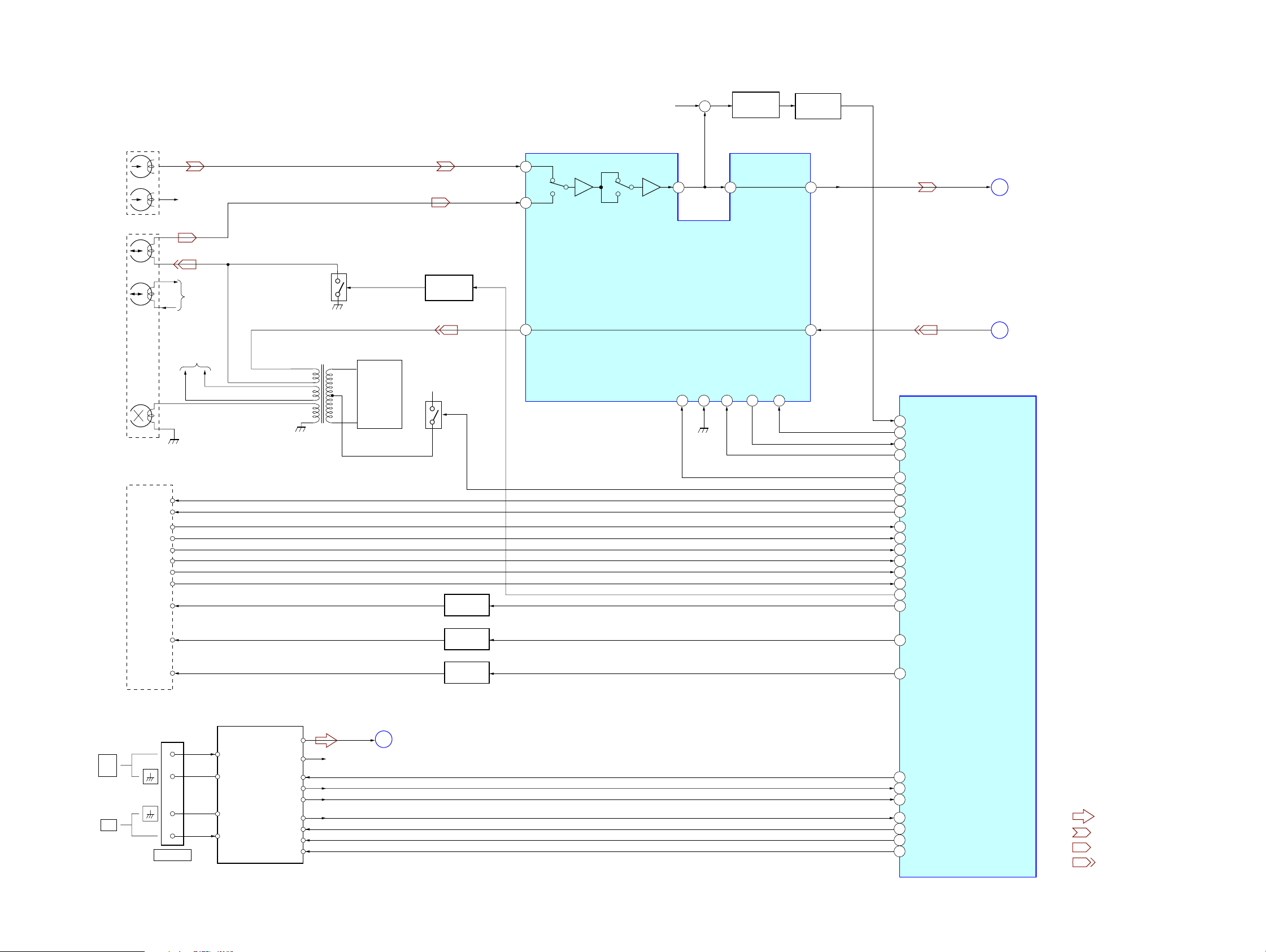
– MAIN SECTION –
GAME
INPUT
DVD
INPUT
DVD
INPUT
AUDIO
VIDEO
VIDEO
VIDEO OUT
FRONT
REAR
CENTER
WOOFER
(Page 22)
(Page 23)
(Page 23)
PHONO
IN
MD IN
J500
L
R
J721
J711
L
R
L
R
+9V
A
B
D
L
R
L
R
CD-L
PB-L
ST-L
J701 (1/2)
R-CH
R-CH
R-CH
J802
MIC1
J801
MIC2
VREF
Q611
R-CH
R-CH
IN4 A
8
IN3
6
IN2
4
IN1
1
10
27
26
77
76
PHONO
EQ AMP
IC601
MUTE
VD-OUT
(75Ω)
VIDEO INPUT
SELECT
IC191
+
(L-R)
(L+R)
SL-IN
C-IN
VC
1
32
RHYTHM
PHRASE
PLAYER
IC461
6db
A/D, D/A
LOGIC
VCA
CONTROL
CENTER
MODE
A+9V
FUNCTION SELECT
SWITCH
IC181
X0
12
X1
14
X2
15
X3
11
AB
10 9
Q181
MUTE
Q471
AMP
IC422 (2/2)
PWML+
22
24
PWML–
2
B
3
C
5
3
2
1
2
1
+
VREF
Q884
X
Q182
20
MUTEOL
28 27
PRO-LOGIC
CONTROL
IC201
4240
SL
11
C
SRSW-IN
MIC AMP
IC850 (1/2)
VC
13
D461
D462
4
TSTB
MCK
6
7
MSD
MLAB
8
MEMP
9
TEMPO
10
XOSXIS
X401
8.19MHz
SOUND
+
10
45
161579
L-IN
SL
SR
MIC AMP
IC850 (2/2)
RV801
MIC LEVEL
X501
32.768kHz
X502
16MHz
172
L
24
REQ
22
DATA
23
SCK
74
LT-IN
VOL OUT SL
VOL OUT C
VR SW IN
2
1
VOL OUT SW
9
3
80
17
VOL
C
VOL
VOL
MIC OUT
GRAPHIC EQUALIZER CONTROL,
INC1
5
INB1
4
INA1
3
IND1
6
INEX1
7
SUR1
42
XC-OUT
11
XC-IN
10
13
X-OUT
X-IN
15
AU-SEL0
71
AU-SEL1
72
66
ML-MUTE
ML-RESET
60
7
PARTY-CLK
6
PARTY-DATA
59
ML-WR
54
ML-BUSY2
42
PARTY-TEMPO
V-SELA
18
100
V-SELB
VIDEO-MUTE
76
77
PL-LAT
78
PL-DAT
PL-CLK
79
(CD MECHANISM CONTROL)
+
INPUT SELECT SWITCH,
ELECTRICAL VOLUME
IC111
INPUT
SELECT
SWITCH
R-CH
AUDIO-OUT
LINE-MUTE
FRONT-RELAY
REAR-RELAY
SYSTEM CONTROLLER
IC501 (3/4)
6 7
MIX AMP
IC422 (1/2)
+
+
EQIC-DAT
EQIC-CLK
TEMP DET
STK-MUTE
HP-MUTE
PROTECT
HP-IN
80
81
97
1
Q802,803
LEVEL SHIFT
82
83
86
88
87
95
85
MUTE
Q281
MUTE
Q271
2
8
MIC
RECB1
SURROUND OR
DPL BUFFER
R-CH
D811
C
A
B
C
A
B
+
MUTE
Q114
10 5
LEVEL SHIFT
Q804, 807, 808
POWER AMP
14 6
IC101(2/2)
24
BASS &
TREBLE
R-CH
POWER AMP
18 11
IC801
STANDBY SWITCH
Q803, 804, 834
POWER AMP
IC101(1/2)
MID/
L+R
REC-L
R-CH
–1
–2
MUTE
Q805,855
RY401
MUTE
Q701
R-CH
SWOUT
OUT1
Q115
R-CH
AC DET
4
FRONT SPEAKER PROTECT
RELAY DRIVE
Q403, 407
24
18
Q166,167
DELAY
Q833
(Page 25)
F
Q923
RELAY DRIVE
Q401, 402
R-CH
D803
DBFB
+
VL
COMMAND
(Page 25)
E
TEMPERATURE
DETECT SWITCH
Q842, 843
TEMPERATURE
DETECT SWITCH
Q831, 832
OVER LOAD
DETECT
Q801, 851
R-CH
IN1
VOLUME
CONTROL
OVER LOAD
Q101, 151, 181
DETECT
CPU
INTERFACE
DATA
D401
D410
CLK
BB-A1
MUTE
Q731
BB-B1
17
PROTECTOR
IC912
OCP
1
VP
2
OUT
3
CT
22 1621
F OUT2
14 15
19
SPEANA
12
TH831
R-CH
+
R-CH
Q805,806
LEVEL SHIFT
+
PROTECT SWITCH
Q431
RY402
R-CH
RY403
R-CH
R-CH
FAN MOTOR
B+
FAN MOTOR
DRIVE
Q961, 962
J701 (2/2)
TM401
+
–
+
–
J891
PHONES
TM402
+
–
+
–
+
–
(Page 23)
C
M901
(FAN)
M
L
R
L
R
J731
SUB WOOFER OUT
L
MD OUT
R
FRONT
SURROUND
CENTER
• R-ch is omitted due to same as L-ch.
• SIGNAL PATH
: TUNER (FM/AM)
: CD PLAY
: TAPE PLAY
: RECORD
: MIC INPUT
24
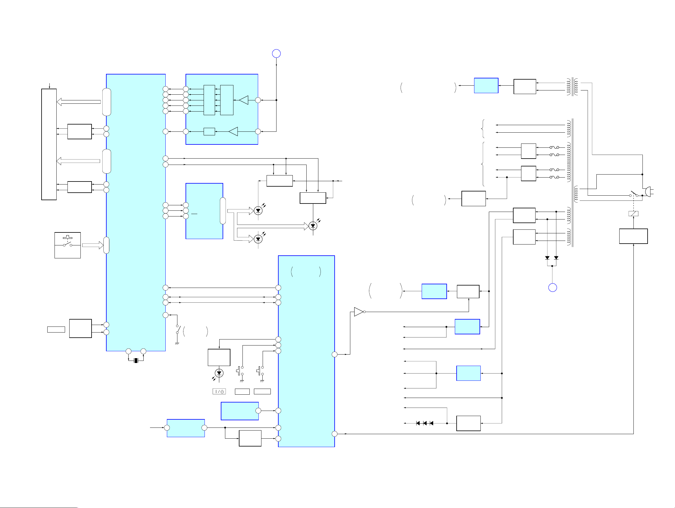
– DISPLAY/KEY CONTROL/POWER SUPPLY SECTION –
FLUORESCENT INDICATOR TUBE DRIVER,
KEY CONTROL
IC601
VF
GRID DRIVE
Q608,609
FL601
FLUORESCENT INDICATOR TUBE
GRID DRIVE
Q606,Q607
S700,S809-817
S801-807,S800
S613-615,S901-909
S908-915,S600-605
S501-504,S612
S701-709,S505-508
43,44
18 – 21,24 – 41
SEG-1 – SEG-25
1
GR-16
8
GR-9
10,9,7-2
16,14 – 12
GR9-GR15
GR-2 ,GR-4-GR8
15
GR-3
17
GR-1
64 – 69
KEY 0 – KEY 5
BPF-F01
BPF-F02
BPF-F03
BPF-F04
BPF-F05
ALL BAND
LED SELB
LED SELA
LED DAT
LED SCK
LED LATCH
RESET
I2C-DATA
I2C-CLK
70
71
72
73
74
75
55
80
78
76
79
77 41
60
61
16
15
14
13
12
11
16
17
18
NFF02
INF03
NFF04
INF05
F06
REC
LEVEL
LED DRIVER
DATA
CLK
STB
BAND-PASS FILTER
IC603
DET
DET
IC701
B.P.F.
P1 – P20
20-29,1-7,9-11
LINE
REC IN
HCD-XGR99AV
(Page 24)
E
SUB POWER
TRANSFORMER
T901
SPEANA
IN
4
6
B+ SWITCH
Q604,605
D501,503
D903,905
D701,703,705
D707,709,711,713,
D801,803,805,807,
D809,811,813
D901
D600
SYSTEM CONTROLLER
OTM-RESET
30
IIC-DATA
29
IIC-CLK
B+ SWITCH
Q602,603
CD MECHANISM
CONTROL
IC501 (4/4)
D502,504
D904,906
D702,704,706,708
D710,712,714
D802,804,806,808
D810,812,814
LED
+3.9V
CD A+5V (SW) ,
CD D+5V (SW)
CD MECHANISM
DECK SECTION
B+
EVER +3.9V
SYSTEM CONTROLLER (IC501) ,
FL DRIVER (IC601) B+
POWER AMP (IC102,IC801),
PROTECT CIRCUIT
–35V
FL DRIVER (IC601)
B–
+5V
REGULATOR
IC921
TO FLUORESCENT
INDICATOR TUBE
(FL601)
REGULATOR
B+ SWITCH
Q921
REGULATOR
–35V
Q903, 908
+5V
IC901
+VL
–VL
+VH
–VH
RECT
D902 – 905
POWER
TRANSFORMER
T951
VF
VF
D853
F963
F964
F961
F962
AC DET
D920
RY901
POWER ON/OFF
RELAY DRIVE
Q901
AC IN
+10
-10
+15
RECT
D832
RECT
D831
RECT
D841 – 844
RECT
D833 – 836
F
(Page 24)
S700
VOLUME
ROTARY
ENCODER
S700
52
D-SW
VOL A
57
56
VOL B
XOUT
XIN
82 83
X601
4MHz
S700
LID (CD)
OPEN/CLOSE
LED
DRIVE
Q601
REMOTE CONTROL
POWER
RECEIVER
S618D602 S617
DISPLAY
1
LED-STBY
75
KEY-POWER
74
KEY-DISPLAY
73
SIRCS
4
CD-POWER
38
IC602
EVER +3.9V
RESET SIGNAL
GENERATOR
IC801
31
RESET
SWITCH
Q801
20
AC-CUT
RESET
12
STBY-RELAY
84
Q922
D+3.9V
ST +9V
(FM/AM TUNER UNIT B+)
TC+9V
FAN MOTOR B+
TC M+9V
(TC MOTOR SECTION B+)
CD M+7V
(CD MOTOR SECTION B+)
LED
3.9V
–VEE
A+9V
D911-913
+3.9V
REGULATOR
IC922
+10V
REGULATOR
IC931
+12V
REGULATOR
Q911,918
25
25
 Loading...