

Page 1
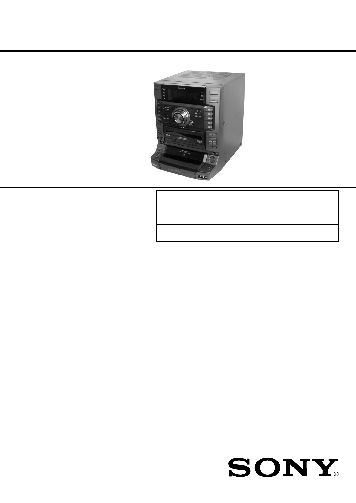
HCD-XGR90AV
SERVICE MANUAL
Ver 1.0 2002.04
• HCD-XGR90AV is the Amplifier,
CD player, tape deck and tuner
section in LBT-XGR90AV.
Model Name Using Similar Mechanism HCD-XGR80
CD CD Mechanism Type CDM37B-30BD60C
Section Base Unit Name BU-30BD60C
Optical Pick-up Name A-MAX.3
TAPE
Section
Model Name Using Similar Mechanism HCD-XGR80
E Model
Australian Model
Amplifier section
Front Speaker:
The following measured at AC 120/220/240 V, 50 Hz
DIN power output (Rated)
150 + 150 watts
(6 ohms at 1 kHz, DIN)
Continuous RMS power output (Reference)
200 + 200 watts
(6 ohms at 1 kHz, 10% THD)
Center Speaker:
DIN power output (Rated) 35 watts
(8 ohms at 1 kHz, DIN)
Continuous RMS power output (Reference)
50 watts
(8 ohms at 1 kHz, 10% THD)
Rear Speaker:
DIN power output (Rated) 35 + 35 watts
(8 ohms at 1 kHz, DIN)
Continuous RMS power output (Reference)
50 + 50 watts
(8 ohms at 1 kHz, 10% THD)
Inputs
GUITAR:
(phone jack) sensitivity 75 mV,
impedance 470 kilohms
PHONO IN:
(phono jacks) sensitivity 3 mV,
impedance 47 kilohms
SPECIFICATIONS
MIX MIC:
(phone jack) sensitivity 1 mV,
impedance 10 kilohms
GAME INPUT:
(phono jacks) sensitivity 250 mV,
impedance 47 kilohms
MD (VIDEO) IN:
(phono jack) sensitivity 450 mV
(250 mV), impedance
47 kilohms
DVD INPUT
FRONT, REAR, CENTER, WOOFER (phono jacks):
sensitivity 450 mV,
impedance 47 kilohms
Outputs
PHONES:
(stereo phone jack) accepts headphones of
8 ohms or more
MD (VIDEO) OUT:
(phono jacks) voltage 250 mV
impedance 1 kilohms
WOOFER OUT (phono jack): voltage 1 V, impedance 1 kilohm
FRONT SPEAKER: accepts impedance of 6 to 16 ohms
CENTER SPEAKER: accepts impedance of 8 to 16 ohms
REAR SPEAKER: accepts impedance of 8 to 16 ohms
— Continued on next page —
COMPACT Hi-Fi STEREO SYSTEM
9-873-955-01
2002D0200-1
© 2002.04
Sony Corporation
Home Audio Company
Published by Sony Engineering Corporation
Page 2
HCD-XGR90AV
Video section
Inputs
VIDEO IN (phono jack): 1 V p-p, 75 ohms
GAME IN (phono jack): 1 V p-p, 75 ohms
Output
VIDEO OUT (phono jack): 1 V p-p, 75 ohms
CD player section
System Compact disc and digital audio system
Laser Semiconductor laser
(λ=795 nm), Emission
duration: continuous
Frequency response 2 Hz – 20 kHz (±0.5 dB)
Signal-to-noise ratio More than 90 dB
Dynamic range More than 90 dB
CD OPTICAL DIGITAL OUT
(Square optical connector jack, rear panel)
Wavelength: 660 nm
Output level –18 dBm
Tape player section
Recording system 4-track 2-channel stereo
Frequency response 40 – 13,000 Hz (±3 dB),
using Sony TYPE I cassette
Tuner section
FM stereo, FM/AM superheterodyne tuner
FM tuner section
Tuning range 87.5 – 108.0 MHz
(50 kHz step)
Antenna FM lead antenna
Antenna terminals 75 ohms unbalanced
Intermediate frequency 10.7 MHz
Notes on chip component replacement
• Never reuse a disconnected chip component.
• Notice that the minus side of a tantalum capacitor may be
damaged by heat.
Flexible Circuit Board Repairing
• Keep the temperature of soldering iron around 270˚C
during repairing.
• Do not touch the soldering iron on the same conductor of the
circuit board (within 3 times).
• Be careful not to apply force on the conductor when soldering
or unsoldering.
CAUTION
Use of controls or adjustments or performance of procedures
other than those specified herein may result in hazardous radiation
exposure.
This appliance is classified as a CLASS 1 LASER product. The
CLASS 1 LASER PRODUCT MARKING is located on the rear
exterior.
AM tuner section
Tuning range
Pan-American model: 530 – 1,710 kHz
(with the interval set at 10 kHz)
531 – 1,710 kHz
(with the interval set at 9 kHz)
Other model: 531 – 1,602 kHz
(with the interval set at 9 kHz)
530 – 1,710 kHz
(with the interval set at 10 kHz)
Antenna AM loop antenna
Antenna terminals External antenna terminal
Intermediate frequency 450 kHz
General
Power requirement
Australian model: 230 – 240 V AC, 50/60Hz
Other model: 120 V, 220 V or 230 –240 V AC,
50/60 Hz
Adjustable with voltage selector
Power consumption 230 watts
Dimensions (w/h/d) Approx. 355 x 425 x 451 mm
Mass : Approx. 15.4 kg
Supplied accessories: AM loop antenna (1)
FM lead antenna (1)
Speaker cords (5)
Speaker pads (12)
Remote commander (1)
Batteries (2)
SAFETY-RELATED COMPONENT WARNING!!
COMPONENTS IDENTIFIED BY MARK 0 OR DOTTED LINE WITH
MARK 0 ON THE SCHEMATIC DIAGRAMS AND IN THE PARTS
LIST ARE CRITICAL TO SAFE OPERATION. REPLACE THESE
COMPONENTS WITH SONY PARTS WHOSE PART NUMBERS
APPEAR AS SHOWN IN THIS MANUAL OR IN SUPPLEMENTS
PUBLISHED BY SONY.
Design and specifications are subject to change without notice.
2
Page 3
HCD-XGR90AV
NOTES ON HANDLING THE OPTICAL PICK-UP
BLOCK OR BASE UNIT
The laser diode in the optical pick-up block may suffer electrostatic
break-down because of the potential difference generated by the
charged electrostatic load, etc. on clothing and the human body.
During repair, pay attention to electrostatic break-down and also
use the procedure in the printed matter which is included in the
repair parts.
The flexible board is easily damaged and should be handled with
care.
NOTES ON LASER DIODE EMISSION CHECK
The laser beam on this model is concentrated so as to be focused on
the disc reflective surface by the objective lens in the optical pickup block. Therefore, when checking the laser diode emission,
observe from more than 30 cm away from the objective lens.
LASER DIODE AND FOCUS SEARCH OPERATION
CHECK
Carry out the “S curve check” in “CD section adjustment” and
check that the S curve waveforms is output three times.
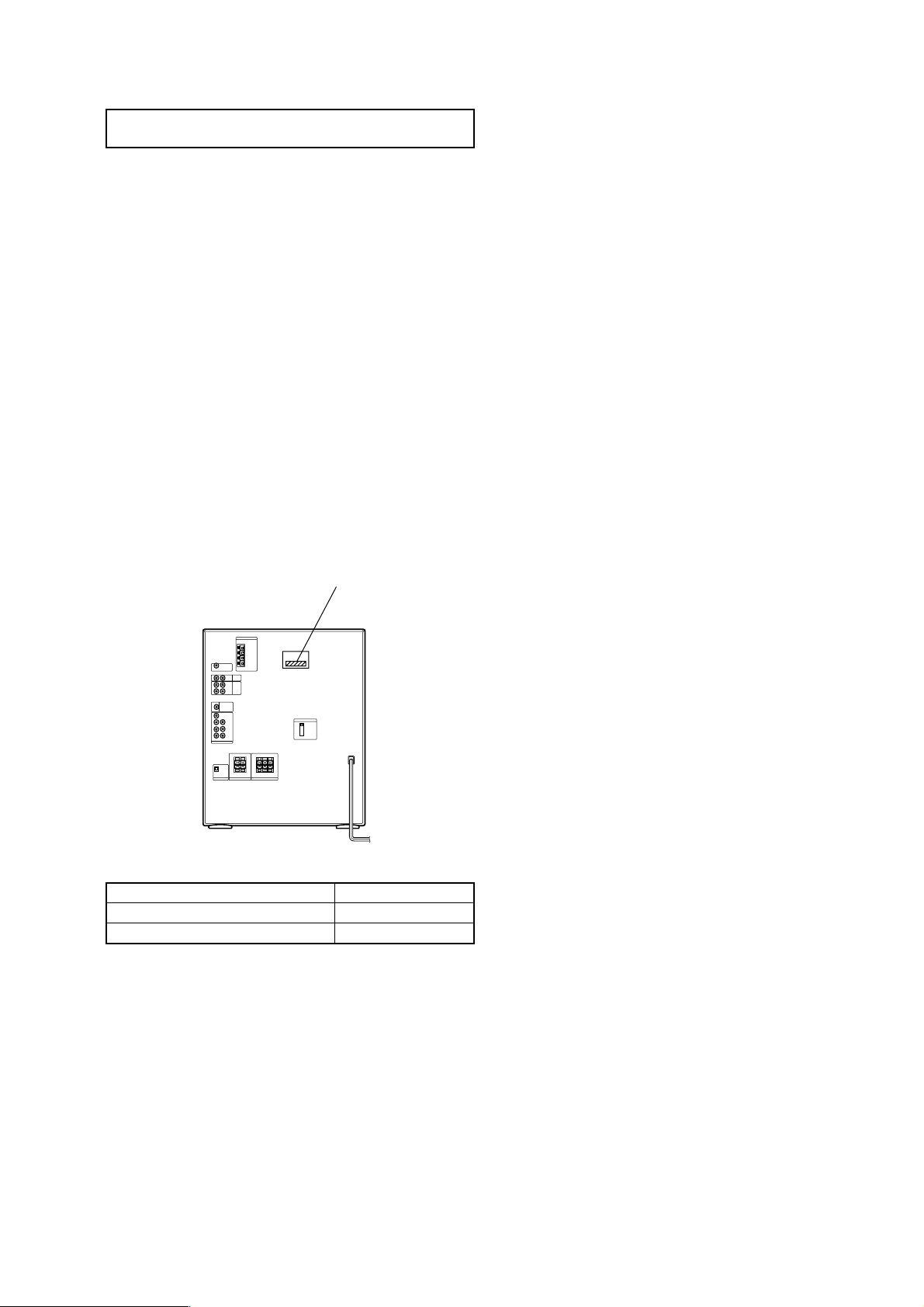
• MODEL IDENTIFICATION
– Rear Panel –
PART No.
MODEL
E model
Australian model
PARTS No.
4-238-825-0s
4-238-825-1s
TABLE OF CONTENTS
1. SERVICING NOTE·························································· 4
2. GENERAL ·········································································· 5
3. DISASSEMBY···································································7
4. TEST MODE ···································································· 15
5. MECHANICAL ADJUSTMENTS ····························· 17
6. ELECTRICAL ADJUSTMENTS ·······························17
7. DIAGRAMS
7-1. Circuit Board Location ······················································21
7-2. Block Diagram – CD Servo Section – ······························· 22
Block Diagram – Tuner/Tape Deck Section – ··················· 23
Block Diagram – Main Section – ······································24
Block Diagram
– Display/Key Control/Power Supply Section –·········· 25
7-3. Printed Wiring Board – BD Section – ·······························26
7-4. Schematic Diagram – BD Section – ·································· 27
7-5. Printed Wiring Board – Motor, LED Section – ················· 28
7-6. Schematic Diagram –Motor, LED Section – ····················· 28
7-7. Schematic Diagram – MIC/Guitar Section – ····················· 29
7-8. Printed Wiring Board – MIC/Guitar Section – ·················· 29
7-9. Schematic Diagram – Main (1/3) Section – ······················ 30
7-10.Schematic Diagram – Main (2/3) Section – ······················31
7-11.Schematic Diagram – Main (3/3) Section – ······················32
7-12.Printed Wiring Board – Main Section – ····························· 33
7-13.Printed Wiring Board
– CD-L,CD-R,Headphone,Front Input,D-SW Section –··34
7-14.Schematic Diagram
– CD-L,CD-R,Headphone,Front Input,D-SW Section –··35
7-15.Printed Wiring Board – Panel VR Section – ······················ 36
7-16.Schematic Diagram – Panel VR Section – ························ 37
7-17.Printed Wiring Board – Panel FL,TC-A,TC-B Section –·38
7-18.Schematic Diagram – Panel FL,TC-A,TC-B Section –·····39
7-19.Printed Wiring Board – PA Section – ································ 40
7-20.Schematic Diagram – PA Section – ··································· 41
7-21. Printed Wiring Board – Sub Amp Section – ·····················42
7-22.Schematic Diagram – Sub Amp Section –························· 43
7-23.Printed Wiring Board – Prologic Section – ······················· 44
7-24.Schematic Diagram – Prologic Section – ·························· 45
7-25. Printed Wiring Board – T rans,Sub T rans Section – ·········· 46
7-26.Schematic Diagram – Trans,Sub T rans Section –··············46
7-27. IC Pin Function Description ············································· 48
7-28. IC Block Diagram ····························································· 53
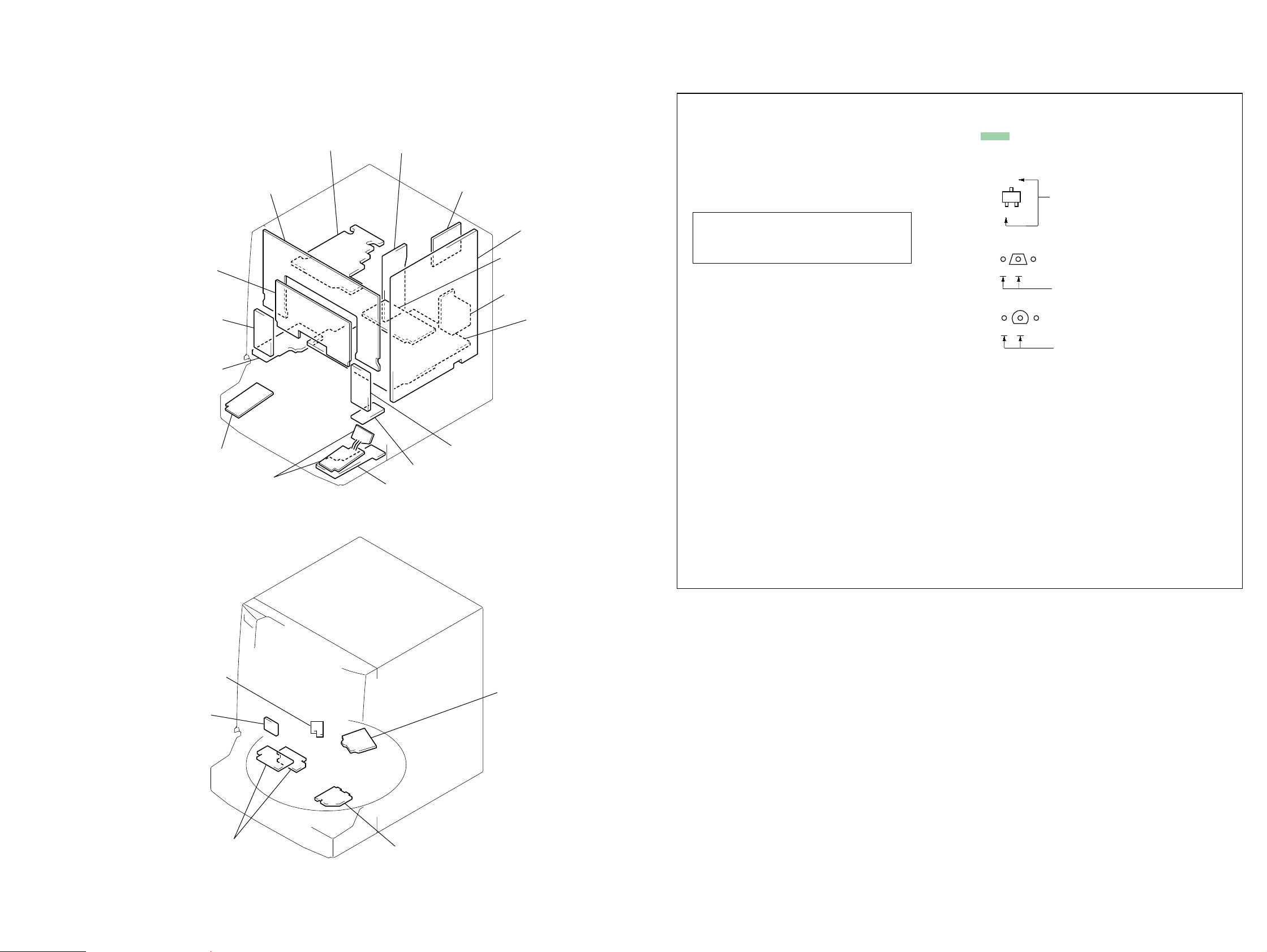
8. EXPLODED VIEWS
8-1. Case,Back Panel Section ··················································· 56
8-2. Front Panel Section-1 ························································ 57
8-3. Front Panel Section-2 ························································ 58
8-4. Chassis Section ·································································· 59
8-5. CD Mechanism Deck Section
(CDM-30BD60C)······························································· 60
8-6. Base Unit Section (BU-30BD60C)···································· 61
9. ELECTRICAL PARTS LIST ······································· 62
3
Page 4
HCD-XGR90AV
SECTION 1
SERVICING NOTE
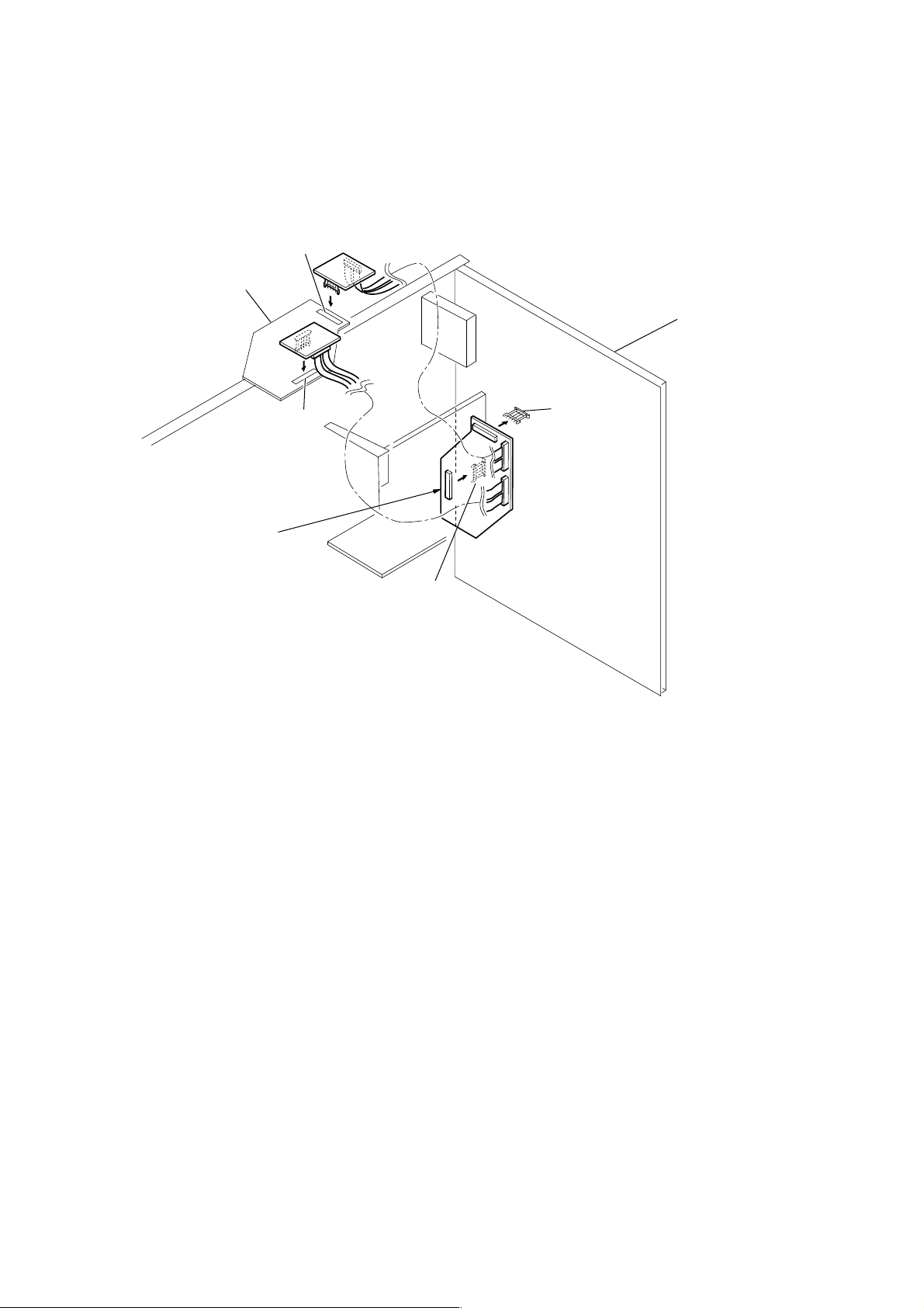
JIG FOR CHECKING PROLOGIC BOARD
The special jig (J-2501-216-A) is useful for checking the PROLOGIC board.
CN201
PROLOGIC board
MAIN board
Jig (J-2501-216-A)
CN202
CN152
CN151
4
Page 5
ALPHABETICAL ORDER
E – G
EDIT (16)
EFFECT (18)
ENTER (9, 16, 19, 20, 21)
FM MODE (13)
FUNCTION (7, 10, 11, 15, 22,
23, 27)
GAME (23)
GAME INPUT AUDIO L/R jacks
(26)
GAME INPUT VIDEO jack
(26)
GAME MIXING (23)
GROOVE (17)
GUITAR DISTORTION (23)
GUITAR jack (23)
GUITAR LEVEL (23)
A EJECT Z/ Z B EJECT
(14)
AMS ./ >
(10, 11)
CD SYNC (15)
Direct equalizer (18)
GUITAR/ROCK/JAZZ/DANCE/
GAME
SALSA/REGGAE/TANGO/
SAMBA/MOVIE
DIRECTION (14, 15, 22)
(10, 11)
DISC SKIP
DISC 1 to 5
DISPLAY
DSP (15, 18)
DVD 5.1CH (27)
H – R
H SPEED DUB (15)
MIC LEVEL (21)
MIX GUITAR/KAROKE (21,
23)
MIX MIC jack (21)
P FILE (18, 19)
PHONES jack
PLAY MODE (10, 11)
POWER SAVE/DEMO
(STANDBY) (24)
Power stream indicator
PRO LOGIC (9, 19)
PUSH OPEN (10)
REPEAT (11)
Main unit
A – D
wj
es
5
5
8
qd
qf
wd
wd
ql
eg
e;
ef
5
w;
ed
3
6
wf
wk
ed
qg
el
e;
ef
eg
wa
ql
qh
eh
ed
(10)
ea
(24)
2
213579qaqs
qd
qf
qg
qh
qj
qk
ql
w;
wa
ws
wd
el
ek
ej
eh
eg
ef
ed
es
wfwgwhwjwkwle;ea
4680
el
wf
ek
SECTION 2
GENERAL
HCD-XGR90AV
This section is extracted from
instruction manual.
5
Page 6
HCD-XGR90AV
S – X
SLEEP (20)
SPECTRUM ANALYZER (21)
SUPER WOOFER (17)
SUPER WOOFER MODE (17)
TIMER SELECT (17, 21)
TUNER/BAND (12, 13, 15)
TUNER ENTER (12)
TUNER MEMORY (12)
TUNING MODE (12, 13)
TUNING –/+ (12, 13)
VOLUME control (11)
X-GROOVE (17)
0
el
qa
9
wg
wg
8
9
7
wh
Remote control
4
el
BUTTON DESCRIPTIONS
1
=/1
/CLOCK SET
c
h/H
x
.m/M>
X
z REC
HX
x
m/M
R/r/T/t
qjej
qk
ws
ws
qjej
qk
ws
(cursor)
qs
qjej
wl
This section is extracted from
instruction manual.
ALPHABETICAL ORDER
C – S
CD (10)
NnN
qj 7
CENTER LEVEL +/– (9)
CLEAR (11)
DISC SKIP (10, 11)
DSP (15, 18)
EFFECT (18)
FILE SELECT –/+ (18)
FUNCTION (10, 11, 15, 22, 23,
PRESET –/+
PRO LOGIC (9, 19)
REAR LEVEL +/– (9)
SLEEP (20)
wd
ws
qs
qa
0
27)
wa
qg
wf
5
9
6
T – V
TAPE A (14)
TAPE B (14)
TEST TONE (9)
TUNER/BAND (12, 13, 15)
TUNING –/+ (12, 13)
TV CH +/– (26)
TV/VIDEO (26)
TV VOL +/– (26)
TV (27)
=/1
VOL +/– (11)
nN
qf
w;
4
wg
3
1
qd
qh
8
wg
wf
wd
BUTTON DESCRIPTIONS
2
=/1
qk
x
ql
X
m/M
./>
1
2
3
ws
4
wa
5
w;
ql
qk
6
7
8
qj
qh
qg
9
0
qa
w;
wa
qf
qs
qd
6
Page 7
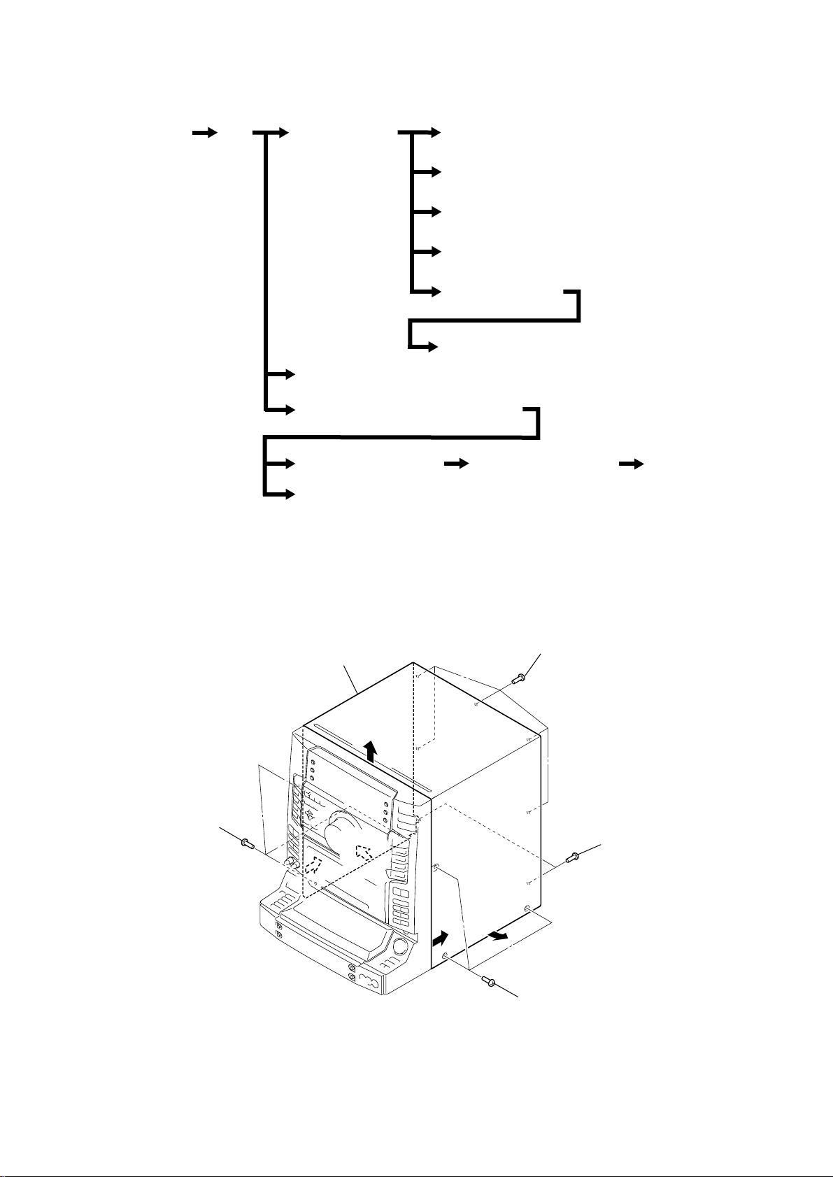
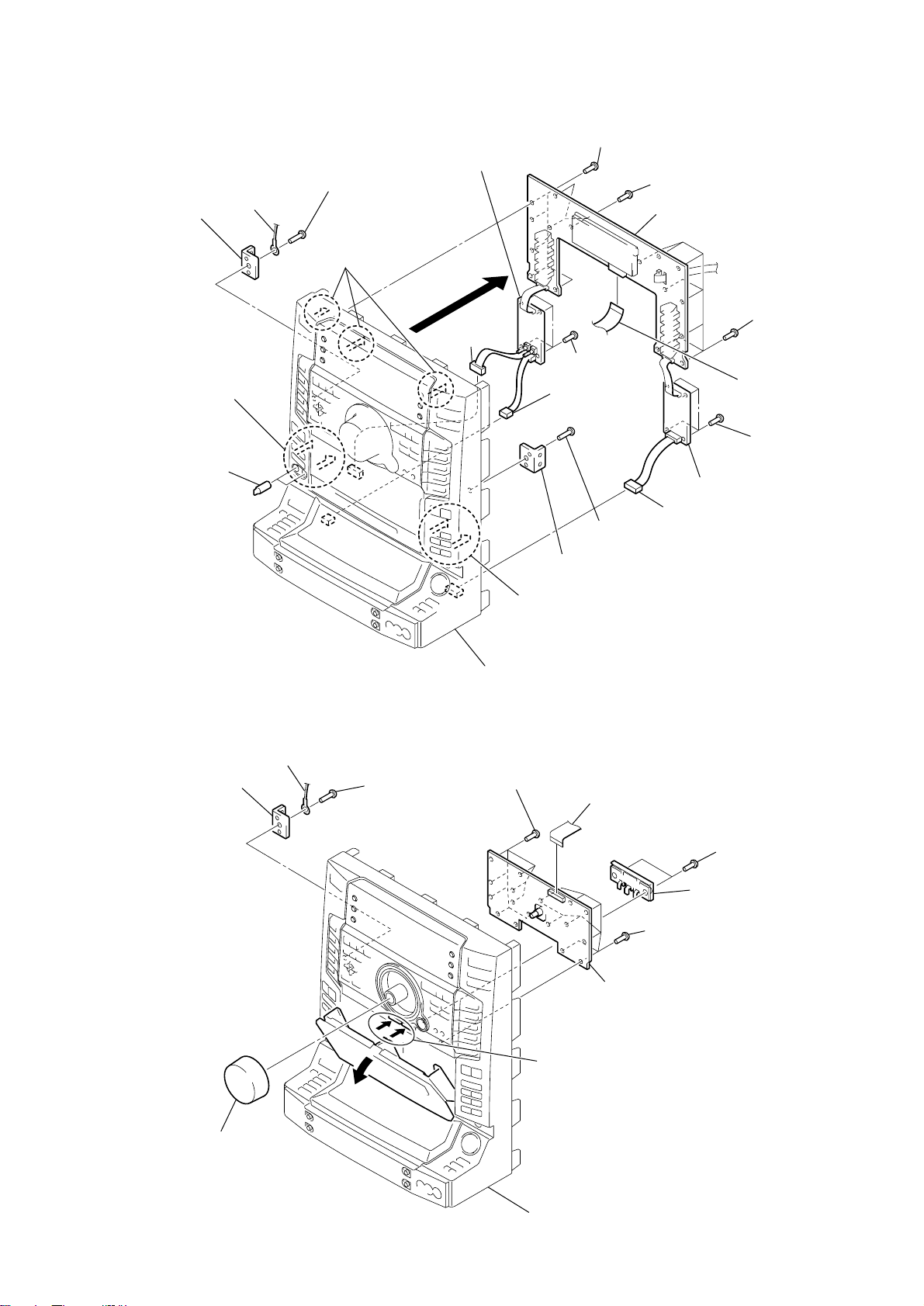
SECTION 3
)
DISASSEMBLY
• The equipment can be removed using the following procedure.
Set Case Front panel section Tape mechanism deck
Back panel, DC fan, MAIN board, PROLOGIC board
CD mechanism deck (CDM37B-30BD60C)
HCD-XGR90AV
PANEL FL board, TC-A board, TC-B board
PANEL VR board
MIC/GUITAR board, HEADPHONE board
FRONT INPUT board
D-SW board, CD-L board, Lid (CD) assy, CD-R board
Base unit-1 (BU-30BD60C)
Disc table
Note : Follow the disassembly procedure in the numerical order given.
3-1. CASE
8
Case
7
1
Three screws
(CASE3 TP2)
5
Base unit-2 (BU-30BD60C) BD board
3
Five screws (BVTT 3
×
6)
4
Two screws (BVTP 3
×
8
6
6
5
2
Three screws (CASE3 TP2)
7
Page 8
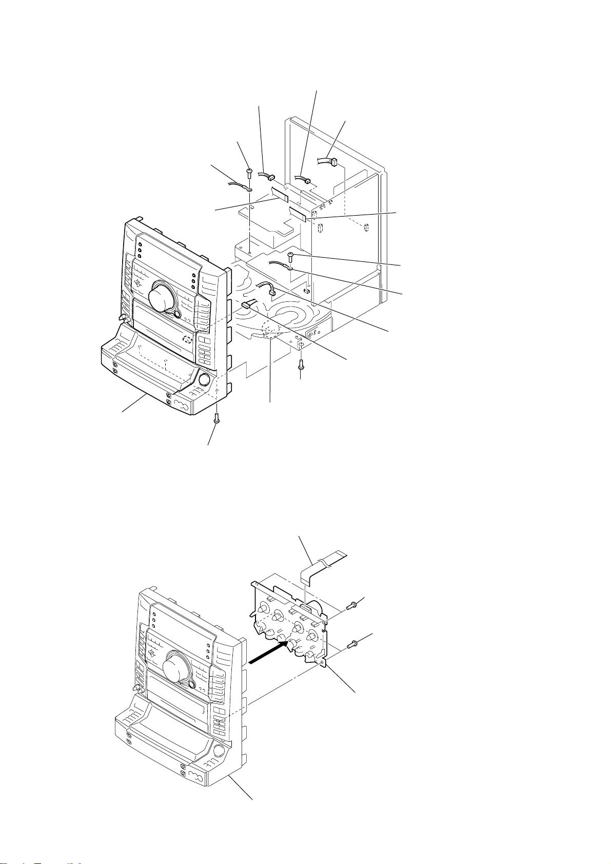
HCD-XGR90AV
)
k
3-2. FRONT PANEL SECTION
2
Flat type wire (CN431)
3
Connector (CN311)
7
Screw (BVTP 3 X 8)
8
Lug
4
Connector (CN903)
5
Connector (CN722)
1
(CN371)
9
0
6
Connector (CN806)
qa
Connector (B deck)
Flat type wire
Screw (BVTP 3 X 8
Lug
qg
Front panel section
3-3. TAPE MECHANISM DECK
qd
Four screws (BVTP 3 X 8)
qs
Screw (BVTP 3 X 8)
qf
Claw
1
Flat type wire (15 core)
4
2
Two screws
(BVTP 2.6 X 8)
3
Two screws
(BVTP 2.6 X 8)
5
Tape mechanism dec
Front panel
8
Page 9
3-4. PANEL FL BOARD, TC-A BOARD, TC-B BOARD
2
Lug
1
Screw (BVTP 2.6 X 8)
qa
Five screws (BVTP 2.6 X 8)
qs
Three screws
(BVTP 2.6 X 8)
qk
PANEL FL board
w;
TC-A board
qd
Eight screws
(BVTP 2.6 X 8)
qg
Four screws
(BVTP 2.6 X 8)
8
Connector (CN703)
6
Connector
(CN812)
7
Connector
(CN704)
ws
TC-B board
0
Two knobs (MIC)
ql
Two claws
4
Screw
(BVTP 2.6 X 8)
qf
Four screws
(BVTP 2.6 X 8)
5
Bracket (TA)
qh
Three claws
3
Bracket (TA)
qj
9
Flat type wire
(CN601)
wa
Two claws
Front panel
y
HCD-XGR90AV
3-5. PANEL VR BOARD
3
Bracket (TA)
2
Lug
1
Screws
(BVTP 2.6 X 8)
7
0
(BVTP 2.6 X 8)
Eight screws
6
Preess the two buttons (EJECT)
5
Flat type wire
(CN701)
qa
(BVTP 2.6 X 8)
qs
PANEL VR board
9
Lever (EJECT) ass
Nine screws
8
Two screws
(BVTP 2.6 X 8)
4
Knob (VOLUME)
Front panel
9
Page 10
HCD-XGR90AV
t
)
3-6. MIC/GUITAR BOARD, HEADPHONE BOARD
1
Connector
(CN812)
2
Two screws
(BVTP 2.6 X 8)
3
MIC bracket
4
MIC/GUITAR board
5
Two screws
(BVTP 2.6 X 8)
6
HEADPHONE bracke
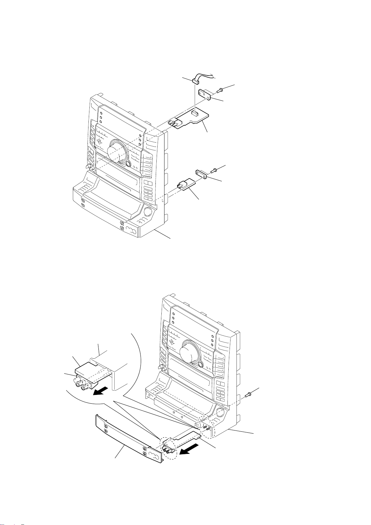
3-7. FRONT INPUT BOARD
Front panel
FRONT INPUT board
J804
Front panel
7
HEADPHONE board
10
2
Bumper (Panel)
3
1
Four screws
(BVTP 2.6 X 8
Front panel
4
FRONT INPUT board
Page 11
3-8. D-SW BOARD, CD-L BOARD, LID (CD) ASSY, CD-R BOARD
)
5
0
Spring (CD)
qa
Lid (CD) assy
9
Sub panel (CD-L) assy
8
CD-L board
7
Four screws
(BVTP 2.6 X 8)
3
Connector
(CN704)
Two screws
(BVTP 2.6 X 8)
6
4
Two screws
(BVTP 2.6 X 8)
ql
Sub panel
(CD-R) assy
qd
Knob
(CD)
qh
qk
CD-R board
qg
Two screws
(BVTP 2.6 X 8)
qs
Connector (CN703)
HCD-XGR90AV
1
Screw (BVTP 2.6 X8)
2
D-SW board
qf
Two screws
(BVTP 2.6 X 8)
qj
Four screws
(BVTP 2.6 X 8)
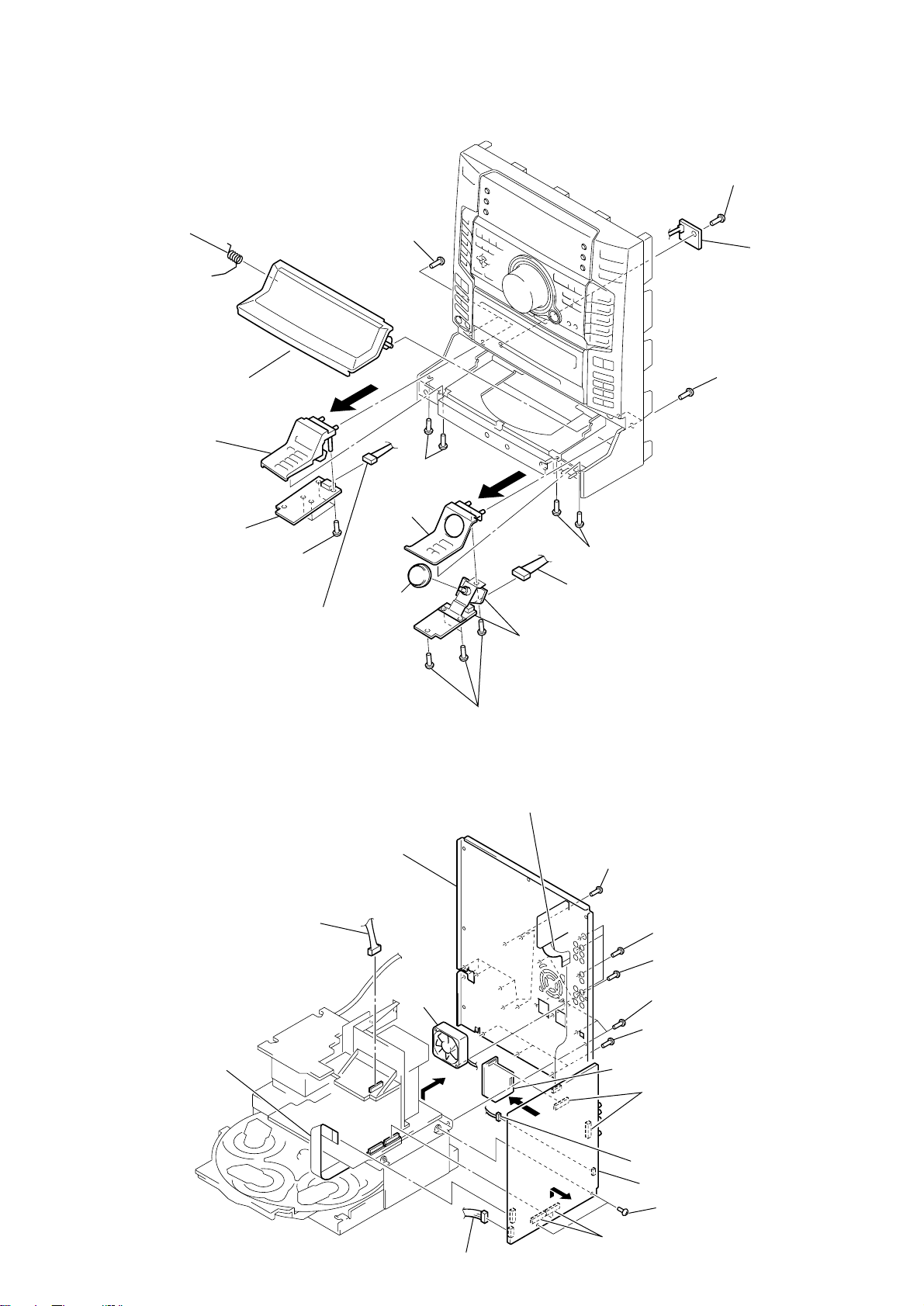
3-9. BACK PANEL, DC FAN, MAIN BOARD, PROLOGIC BOARD
1
Flat type wire (CN441)
7
Back panel
qd
Connector (CN102)
q;
DC FAN
(M901)
qa
Flat type wire
(CN401)
6
qs
Connector (CN441)
qk
2
Eight screws
(BVTP 3 X 8)
ql
PROLOGIC board
8
qg
Two connectors
(CN901, 902)
3
Four screws
(BVTP 3 X 8)
9
Two screws
(BVTP 3 X 8)
5
Four screws
(BVTP 3 X 8)
4
Three screws
(BVTP 3 X 8)
qj
Two connectors
(CN151, 152)
Connector (CN961
qh
MAIN board
qf
Two screws
(BVTP 3 X 8)
11
Page 12
HCD-XGR90AV
m
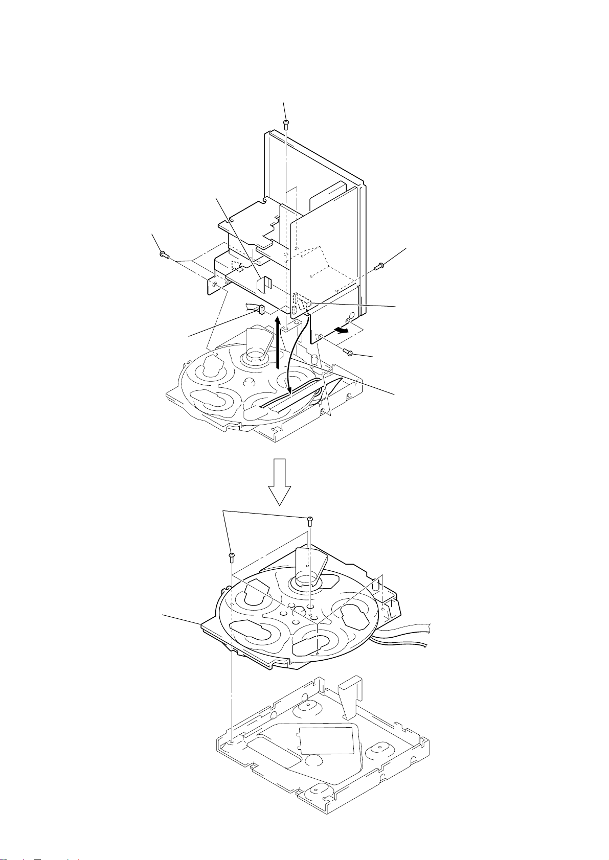
3-10. CD MECHANISM DECK (CDM37B-30BD60C)
1
Flat type wire
(CN401)
4
Three screws
(BVTP 3 X 8)
7
2
Connector
(CN411)
6
Two screws (BVTP 3 X 8)
8
7
3
Four screws (BVTP 3 X 8)
Wire holder
5
Two screws
(BVTP 3 X 8)
qa
CD mechanism deck
(CDM37B-30BD60C)
0
Five screws
(BVTP3 × 8)
9
Remove two cables fro
wire holder.
12
Page 13
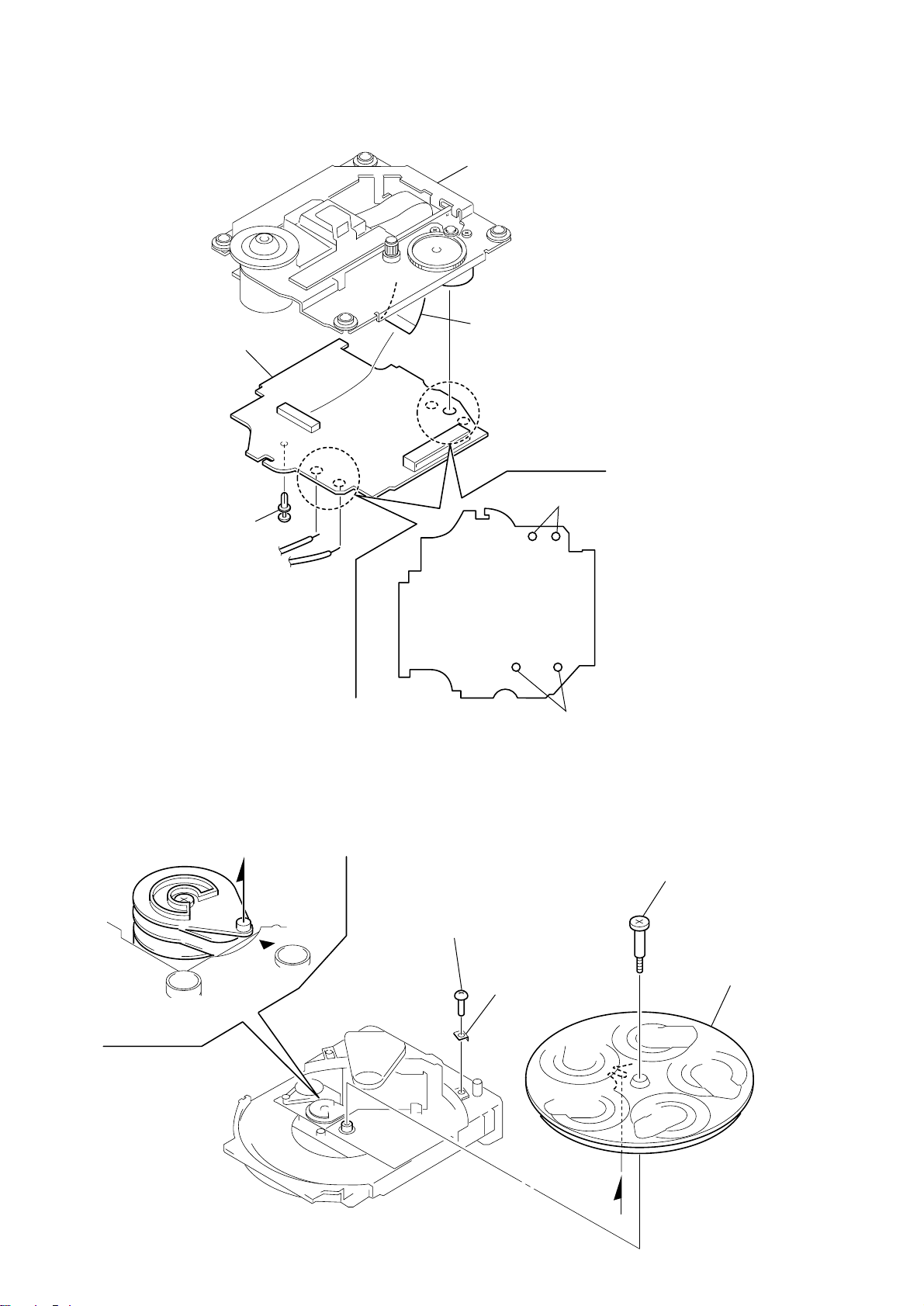
3-11. BASE UNIT-1 (BU-30BD60C)
)
2
Boss
3
Base unit
(BU-30BD60C)
1
BU fitting screw
HCD-XGR90AV
3-12. BASE UNIT-2 (BU-30BD60C)
1
Two floating screws (DIA.12)
4
Two coil springs
(insulator)
6
Base unit (BU-30BD60C)
2
Two screws
(BVTP 2.6 X 8)
3
Two stoppers
(BU)
Holder (BU30) assy
5
Two coil
springs
(insulator
13
Page 14
HCD-XGR90AV
e
3-13. BD BOARD
5
BD board
BU-30BD60C
4
Flat type wire (CN102)
3
Rivet
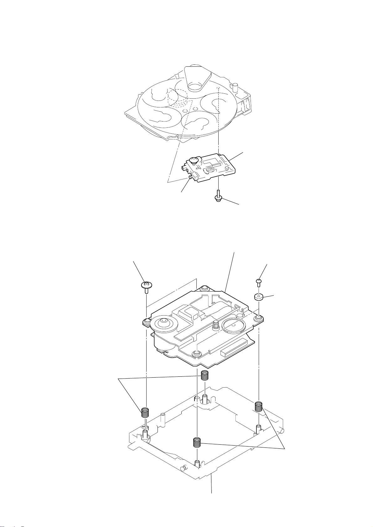
3-14. DISC TABLE
Note: When the disc table is installed, adjust the positions of roller cam
and mark B as shown in the figure, then set to the groove of disc
table.
A
1
Screw (BVTP 3
1
Remove the two solders.
2
Remove the two solders.
×
8)
3
Step screw
14
2
Bracket (BU)
A
4
Disc tabl
Page 15
SECTION 4
B
TEST MODE
HCD-XGR90AV
[MC Cold Reset]
• The cold reset clears all data including preset data stored in the
RAM to initial conditions. Execute this mode when returning
the set to the customer.
Procedure:
1. Turn the power ON or set to the DEMO mode.
2. Press three buttons of c/CLOCK SET , TUNER ENTER ,
and \/1 simultaneously.
3. The set is reset, and displays “COLD RESET”, then becomes
DEMO mode.
[Change-over the AM Tuning Interval]
• The AM tuning interval can be changed over 9 kHz or 10 kHz.
Procedure:
1. Press the \/1 button to turn the power ON.
2. Select the function “TUNER”, and press the TUNER/BAND
button to select the BAND “AM”.
3. Press the \/1 button to turn the power OFF.
4. Press the ENTER/NEXT and \/1 buttons simultaneously,
and the display on the fluorescent indicator tube changes to
“AM 9 K STEP” or “AM 10 K STEP”, and thus the tuning
interval is changed over.
[CD Ship Mode] (No memory clear)
• This mode moves the optical pick-up to the position durable to
vibration. Use this mode when returning the set to the customer
after repair.
Procedure:
1. Press the \/1 button to turn the power ON.
2. Press the EDIT and
3. A message “LOCK” is displayed on the fluorescent indicator
tube, and the CD delivery mode is set.
[LED and Fluorescent Indicator Tube All Lit, Key Check
Mode]
Procedure:
1. Press three buttons of c/CLOCK SET , ENTER/NEXT ,
and DISC 2 simultaneously.
2. LEDs and fluorescent indicator tube are all turned on.
3. Press the DISC 1 button, the MODE and DESTINATION are
displayed fluorescent indicator tube.
4. Each time the DISC 1 button is pressed, the MC/GC category
version is displayed in the following order.
5. Press the DISC 2 button, and the key check mode is acti-vated.
NR MC GC CD CDDM CDMA
6. In the key check mode, the fluorescent indicator tube displays
“K 0 J0 V0”. Each time a button is pressed, “K” value in-creases
to “K69”call the button is pressed.However, once a button is
pressed, it is no longer taken into account.
“J” value increases like 1, 2, 3 ... if turn the . AMS >
JOG dial clock-wise,or it decreases like 0, 9, 8 ... if turn the
. AMS > JOG dial counter-clockwise.
“V” value increases like 1, 2, 3 ... if turn the VOLUME dial
clockwise (“+” direction), or it decreases like 0, 9, 8 ... if turn
the VOLUME dial counterclockwise (“–” direction).
7. To release from this mode, press three buttons in the same
manner as step 1, or disconnect the power cord.
buttons simultaneously.
\/1
BDABDBSTTATMTC
CDM
[Sled Servo Mode] (CD service mode)
• This mode can run the CD sled motor freely. Use this mode, for
instance, when cleaning the pick-up.
Procedure:
1. Select the function “CD”.
2. Press three buttons c/CLOCK SET , TUNER ENTER , and
DISC 5 simultaneously.
3. The Sled Servo mode is selected, if “CD” is blanking on the
fluorescent indicator tube.
4. With the CD in stop status, press M button in CD section to
move the pick-up to outside track, or m button to inside track.
5. To exit from this mode, press
OFF.
Note:
• Always move the pick-up to most inside track when exiting from
this mode. Otherwise, a disc will not be unloaded.
• Do not run the sled motor excessively, otherwise the gear can
be chipped.
[Change-over of FUNCTION Name]
• The FUNCTION name of external input terminal can be changed
over to VIDEO or MD. W ith the FUNCTION selected to “MD”,
about 5dB mute is applied to the input gain.
Procedure:
1. Press \/1 button to turn the power OFF.
2. Press
several seconds, and the power is turned on, the display of
fluorescent indicator tube changes to “MD” or “VIDEO”
instantaneously, and thus the FUNCTION is changed over.
[Aging Mode]
This mode can be used for operation check of tape deck section.
Tape deck section work in parallel.
• If an error occurred:
The aging operation stops and display then status.
• If no error occurs:
The aging operation continues repeatedly.
Procedure:
1. Load the tapes into the decks A and B respectively.
2. Press the FUNCTION button to select the function “CD”.
3. Press the PLAY MODE button to set the “ALL DISCS” mode,
and press the REPEAT button to “REPEAT” off.
4. Press three buttons of c/CLOCK SET , TUNER ENTER ,
and DISC 4 simultaneously.
5. The aging mode is activated, if the indicator of disc tray number on the fluorescent indicator tube is blinking.
6. To release from the aging mode, press the \/1 button to turn
the power OFF and operate the cold reset. (Refer to the “MC
Cold Reset”)
1. Display at the Aging Mode
• Display operating state of tape deck section alternately.
• If an error occurred, stop display.
button together with FUNCTION button for
\/1
button turn to the power
\/1
15
Page 16
HCD-XGR90AV
2. Tape Deck Section
• The sequence during the aging mode is following as below.
• If an error occurred, stop display that step.
Aging mode sequence (Tape deck section):
Rewind the tape A
“T APE A AG-1”
Shut off
FWD the tape A
“T APE A AG-2”
2 minutes
Fast forward the tape A
“T APE A AG-3”
Shut off or 20 seconds
RVS the tape A
“T APE A AG-4”
2 minutes
Rewind the tape A
“T APE A AG-5”
Shut off
3. CD Section
• The sequence during the aging mode is following as below.
• If an error occurred, stop display that step.
Aging mode sequence (CD section):
Tray T urn
DISC 1
chucking
TOC Read
Track 1 Play
2 seconds
Last Track Play
2 seconds
FWD the tape B
“TAPE B AG-2”
2 minutes
Fast forward the tape B
“TAPE B AG-3”
Shut off or 20 seconds
RVS the tape B
“TAPE B AG-4”
2 minutes
Rewind the tape B
“TAPE B AG-5”
Shut off
Note: “TAPE * AG- * ” is display of each step.
Tray Tun
DISC 4
Chucking
TOC Read
Track 1 Play
2 seconds
Last Track play
[VACS ON/OFF]
• The volume control by VACS is turned ON/OFF.
Procedure:
1. Press the \/1 button to turn the power ON.
2. Press the PLAY MODE and \/1 buttons simultaneously.
3. The reaction display appears when switcing ON/OFF.
16
Page 17
HCD-XGR90AV
SECTION 5
MECHANICAL ADJUSTMENTS
Precaution
1. Clean the following parts with a denatured alcohol-moistened
swab:
record/playback heads pinch rollers
erase head rubber belts
capstan idlers
2. Demagnetize the record/playback head with a head demagnetizer.
3. Do not use a magnetized screwdriver for the adjustments.
4. After the adjustments, apply suitable locking compound to the
parts adjusted.
5. The adjustments should be performed with the rated power supply voltage unless otherwise noted.
Torque Measurement
Mode Torque Meter Meter Reading
2.9~6.9 mN•m
FWD (30 to 70 g•cm)
CQ-102C
FWD
back tension (2 to 6 g•cm)
FF/REW CQ-201B (80 to 170 g•cm)
(0.42 – 0.97 oz•inch)
0.19~0.59 mN•m
(0.03 – 0.08 oz•inch)
7.8~16.7 mN•m
(1.11 – 2.36 oz • inch)
SECTION 6
ELECTRICAL ADJUSTMENTS
DECK SECTION 0 dB = 0.775 V
Precaution
1. Demagnetize the record/playback head with a head demagnetizer.
2. Do not use a magnetized screwdriver for the adjustments.
3. After the adjustments, apply suitable locking compound to the
parts adjust.
4. The adjustments should be performed with the rated power
supply voltage unless otherwise noted.
5. The adjustments should be performed in the order given in
this service manual. (As a general rule, playback circuit
adjustment should be completed before performing recording
circuit adjustment.)
6. The adjustments should be performed for both L-CH and R-CH.
7. Switches and controls should be set as follows unless otherwise specified.
8. Set to the DOLBY NR OFF.
9. Set to the test mode.
(1) Press the \/1 button to turn the power ON.
(2) Select the function “TAPE A or B”.
(3) Press the button of c/CLOCK SET , TUNER ENTER ,
and DISC 3 simultaneously, to set the tape deck test mode
and displays “TEST MODE” on the fluorescent indicator
tube.
(4) To release from the test mode, press the \/1 button.
• Test Tape
Tape Signal Used for
P-4-A100 10 kHz, – 10 dB Azimuth Adjustment
WS-48B 3 kHz, 0 dB Tape Speed Adjustment
17
Page 18
HCD-XGR90AV
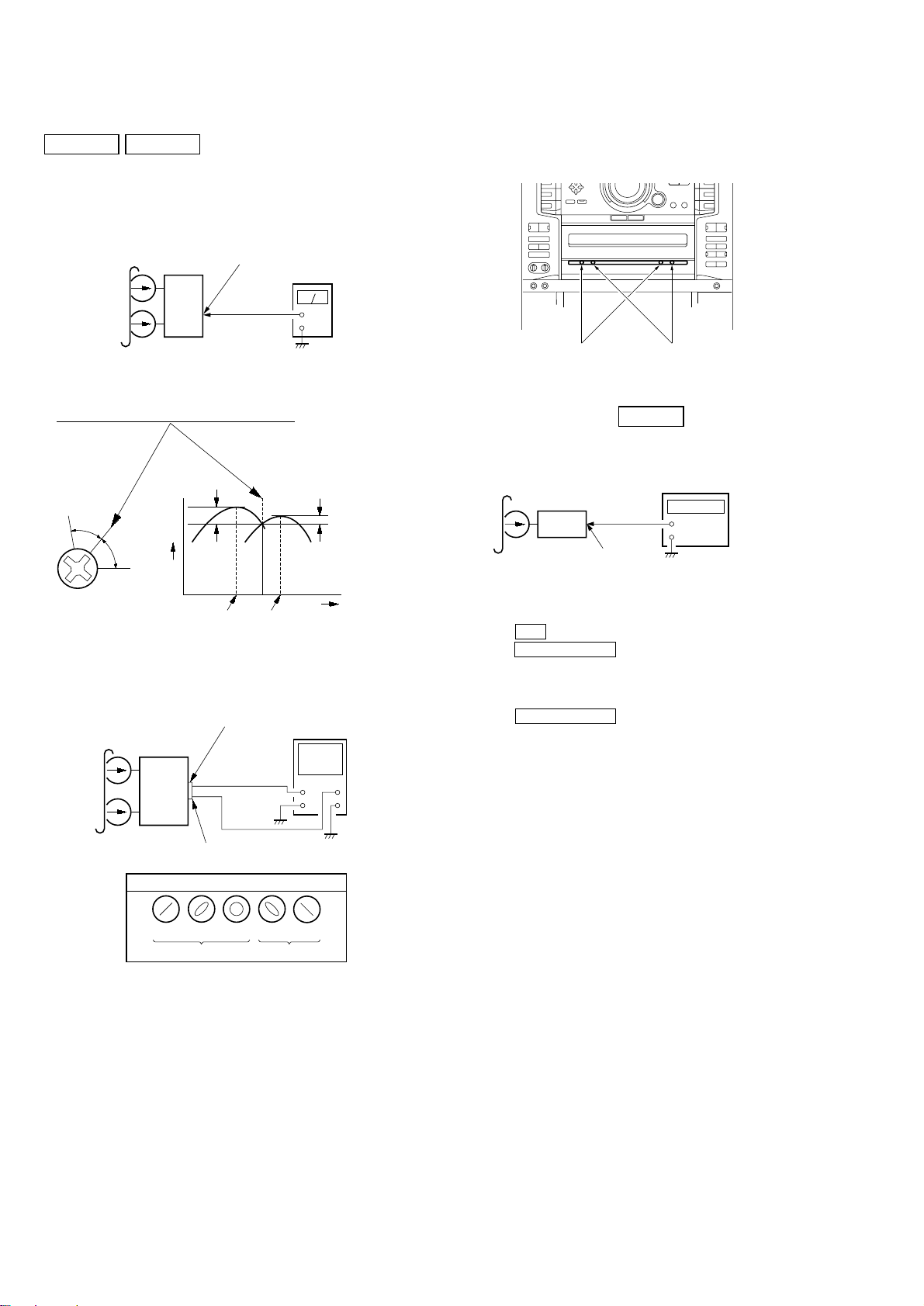
)
Record/Playback Head Azimuth Adjustment
DECK A DECK B
Note: Perform this adjustments for both decks
Procedure:
1. Mode: Playback (FWD)
test tape
P-4-A100
(10 kHz, – 10 dB)
MAIN board
MD (VIDEO) OUT jack (J701
L-CH, R-CH
level meter
set
+
2. Turn the adjustment screw and check output peaks. If the peaks
do not match for L-CH and R-CH, turn the adjustment screw
so that outputs match within 1dB of peak.
Output
level
within
1dB
L-CH
peak
R-CH
peak
within
1dB
Screw
position
L-CH
peak
Screw
position
R-CH
peak
3. Mode: Playback
MAIN board
test tape
P-4-A100
(10 kHz, – 10 dB)
L-CH
set
R-CH
MD (VIDEO) OUT jack (J701)
L-CH
R-CH
oscilloscope
V
H
Adjustment Location: Playback Head (Deck A).
Record/Playback/Erase Head (Deck B).
forward
reverse
Tape Speed Adjustment DECK B
Mode: Playback
test tape
WS-48B
(3 kHz, 0 dB)
set
MAIN board
MD (VIDEO) OUT jack (J701)
L-CH, R-CH
frequency counter
+
–
1. Insert the WS-48B into the deck B.
2. Press the H button on the deck B.
3. Press the H SPEED DUB button in playback mode.
Then at HIGH speed mode.
4. Adjust RV392 on the LEAF SW board do that frequency
counter reads 6,000 ± 180 Hz.
5. Press the H SPEED DUB button.
Then back to NORMAL speed mode.
6. Adjust RV391 on the LEAF SW board so that frequency
counter reads 3,000 ± 90 Hz.
Adjustment Location: MAIN board
Sample value of Wow and Flutter: 0.3% or less W.RMS (JIS)
(WS-48B)
waveform of oscilloscope
in phase 45°90°135°180
good
wrong
°
4. Repeat step 1 to 3 in playback (REV) mode.
5. After the adjustments, apply suitable locking compound to the
pats adjusted.
18
Page 19
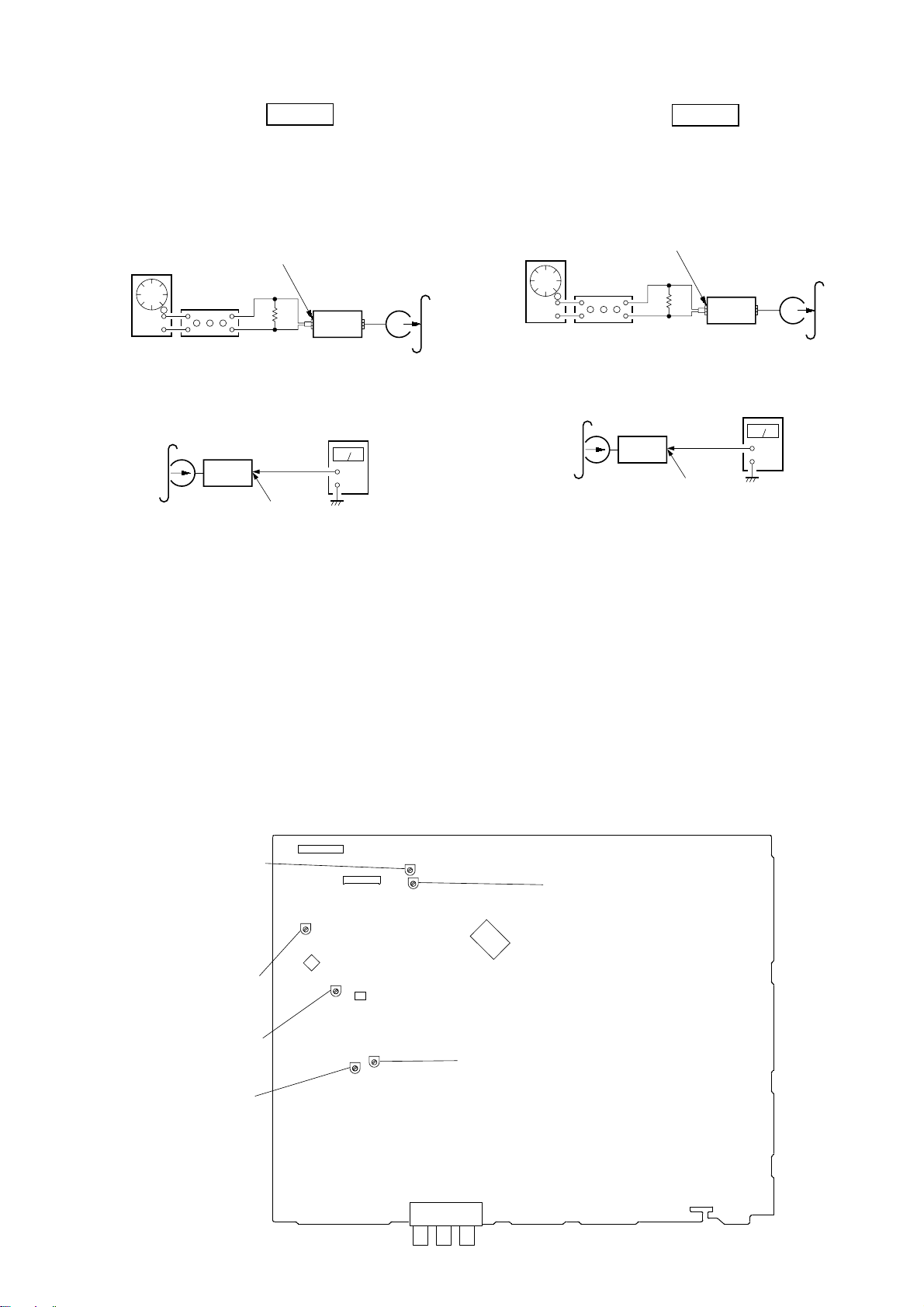
HCD-XGR90AV
e
r
+
–
set
recorded
portion
MAIN board
CN301 pin
1
(L-CH)
pin
3
(R-CH)
level meter
REC Bias Adjustment DECK B
Procedure:
1. Mode: Record
FUNCTION: VIDEO
MAIN board
MD(VIDEO) IN jack (J701)
L-CH, R-CH
50 mV (– 23.8 dB)
600
Ω
blank tap
CS-123
AF OSC
1) 315 Hz
2) 10 kHz
attenuator
set
2. Mode: Playback
recorded
portion
set
MAIN board
CN301 pin
pin
level mete
1
(L-CH)
3
(R-CH)
+
–
3. Confirm playback the signal recorded in step 1 become specification values as follows.
If these values are out of specification values, adjust the R V321
(L-CH) and RV322 (R-CH) on the MAIN board to repeat
steps 1and 2.
Adjustment level: The playback output of 10kHz level difference
against 315 Hz reference should ±0.5 dB.
Adjustment Location: MAIN board
REC Level Adjustment DECK B
Procedure:
1. Mode: Record
FUNCTION: VIDEO
MAIN board
MD (VIDEO) IN jack (J701)
L-CH, R-CH
AF OSC
315 Hz, 50 mV (– 23.8 dB)
600
Ω
blank tape
CS-123
attenuator
set
2. Mode: Playback
3. Confirm playback the signal recorded in step 1 become specification values as follows.
If these values are out of specification values, adjust the R V351
(L-CH) and RV301 (R-CH) on the MAIN board to repeat steps
1 and 2.
Specification values:
CN301 playback level: 47.2 to 53.0 mV (– 24.3 to – 23.3 dB)
Adjustment Location: MAIN board
– MAIN BOARD (Component Side) –
RV392
TAPE SPEED
(HIGH)
RV301
REC LEVEL
(R-CH)
RV351
REC LEVEL
(L-CH)
RV321
REC BIAS
(L-CH)
1
CN371
IC301
19
1
CN431
1
CN301
RV391
15
TAPE SPEED
(NORMAL)
IC501
3
RV322
REC BIAS
(R-CH)
IN
OUT
MD (VIDEO)
19
Page 20
HCD-XGR90AV
e
)
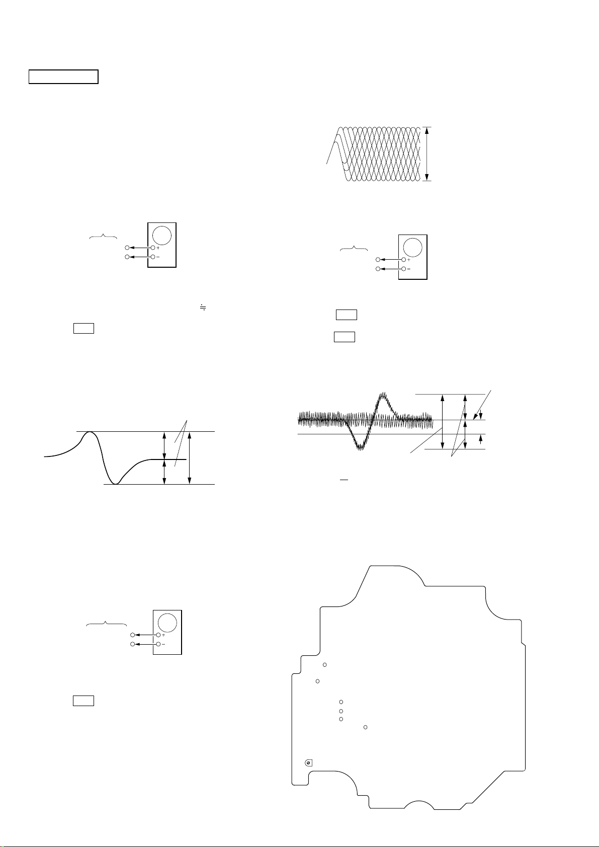
CD SECTION
Note :
1. CD Block is basically designed to operate without adjustment.
Therefore, check each item in order given.
2. Use LUV-P01 (4-999-032-01) unless otherwise indicated.
3. Use an oscilloscope with more than 10M impedance.
4. Clean the object lens by an applicator with neutral detergent
when the signal level is low than specified value with the
following checks.
S-Curve Check
Oscilloscope
BD board
TP(FE)
TP(DVC)
Procedure :
1. Connect oscilloscope to TP (FE).
2. Connect between TP (FE) and TP (DVC ( 1.65 V)) by lead
wire.
3. Press the \/1 button to turn the power ON.
4. Load a disc (LUV -P01) and actuate the focus search. (In consequence of open and close the disc tray, actuate the focus search)
5. Confirm that the oscilloscope waveform (S-curve) is symmetrical between A and B. And confirm peak to peak level within 2
±0.5 Vp-p.
S-curve waveform
symmetry
A
±
within 4
B
1Vp-p
Note: Clear RF signal waveform means that the shape “◊” can be
clearly distinguished at the center of the waveform.
VOLT/DIV : 200mV
TIME/DIV : 500ns
±
level : 1.45
0.3Vp-p
E-F Balance (1 Track jump) Check
oscilloscop
BD board
TP(TE)
TP(DVC)
Procedure:
1. Connect oscilloscope to TP (TE) and TP (DVC) board.
2. Press the \/1 button to turn the power ON.
3. Load a disc (LUV-P01) and playback the number nine track.
4. Press the bB button. (Becomes the 1track jump mode.)
5. Confirm that the level B and A (DC voltage) on the oscilloscope waveform.
center of
waveform
B
0V
B=1.3 ± 0.6Vp-p
Specified level: × 100=less than – 22%
A
B
symmetry
A (DC voltage
6. After check, remove the lead wire connected in step 2.
Note : • Try to measure several times to make sure than the ratio
of A : B or B : A is more than 10 : 7.
• Take sweep time as long as possible and light up the
brightness to obtain best waveform.
RF Level Check
oscilloscope
BD board
TP2(RFDC)
TP1(RFAC)
Procedure :
1. Connect oscilloscope to TP2 (RFDC) and TP1 (RFAC).
2. Press the \/1 button to turn the power ON.
3. Load a disc (LUV-P01) and playback.
4. Confirm that oscilloscope waveform is clear and check RF
signal level is correct or not.
6. Adjust RV101 so that A (DC voltage) becomes 0.
Checking Location:
[BD BOARD]
DVC
RFAC
FE
SE
TE
RFDC
RV101
20
Page 21
d
7-1. CIRCUIT BOARD LOCATION
HCD-XGR90AV
SECTION 7
DIAGRAMS
PANEL VR board
TC-A board
MIC/GUITAR board
CD-L board
PANEL FL board
CD-R board
TRANS board
SUB TRANS board
TUNER PACK
(FM/AM TUNER UNIT)
HEADPHONE board
FRONT INPUT board
TC-B board
MAIN board
SUB AMP board
PROLOGIC boar
PA board
Note on Schematic Diagram:
• All capacitors are in µF unless otherwise noted. pF: µµF
50 WV or less are not indicated except for electrolytics
and tantalums.
• All resistors are in Ω and 1/
specified.
2
•
• 5 : fusible resistor.
• C : panel designation.
• A : B+ Line.
• B : B– Line.
• H : adjustment for repair.
• Voltages and waveforms are dc with respect to ground
• Voltages are taken with a VOM (Input impedance 10 MΩ).
• Waveforms are taken with a oscilloscope.
• Circled numbers refer to waveforms.
• Signal path.
• Abbreviation
: nonflammable resistor.
Note:
The components identified by mark 0 or dotted line
with mark 0 are critical for safety.
Replace only with part number specified.
under no-signal conditions.
BD board section
no mark: CD PLAY
Other board section
no mark: TUNER (FM/AM)
( ): TAPE PLAY
< >: TAPE REC
[ ]: CD PLAY
Voltage variations may be noted due to normal production tolerances.
Voltage variations may be noted due to normal production tolerances.
F : TUNER (FM/AM)
E : TAPE PALY (DECK A)
d : TAPE PALY (DECK B)
G : RECORD
J : CD PALY (ANALOG OUT)
c : CD PALY (DIGITAL OUT)
N : MIC INPUT
AUS : Australian model
4
W or less unless otherwise
Note on Printed Wiring Boards:
• X : parts extracted from the component side.
• : Pattern from the side which enables seeing.
(The other layers´ Patterns are not indicated.)
• Indication of transistor.
C
B
B
B
Q
E
Q
CE
These are omitted.
These are omitted.
Q
CE
These are omitted.
SENSOR board
D-SW board
MOTOR board
BD board
LED board
2121
Page 22
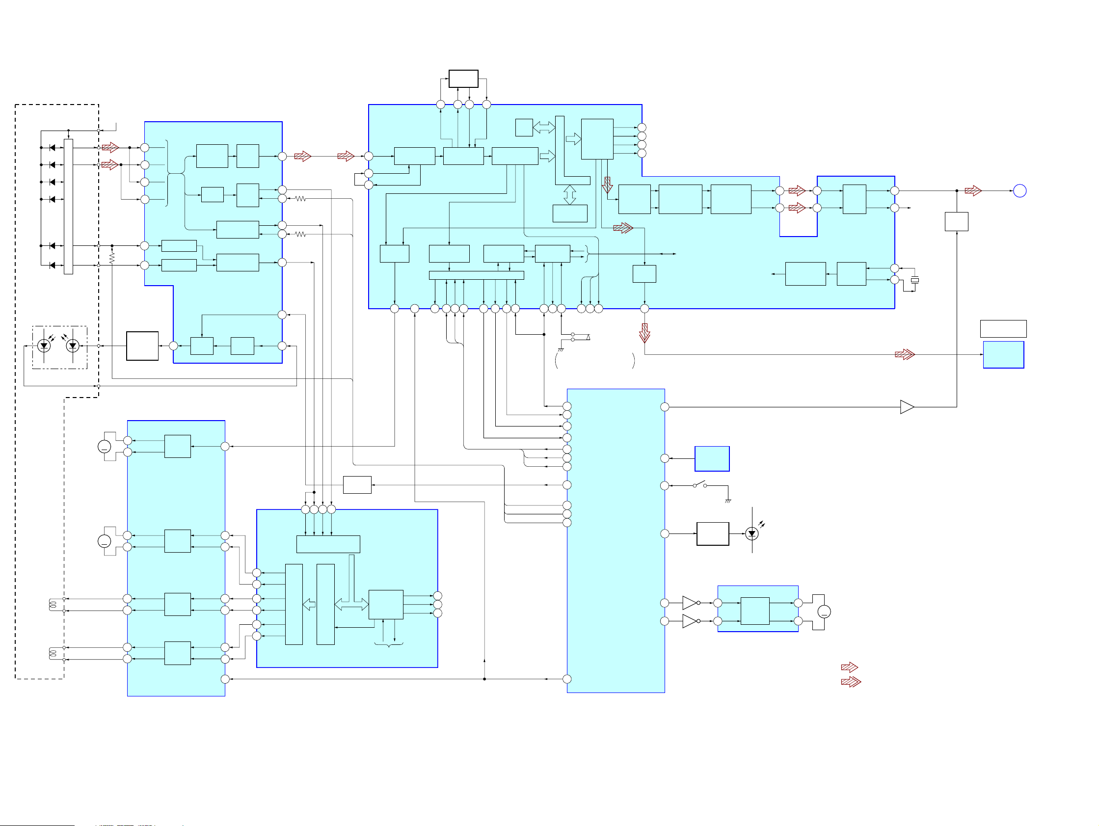
HCD-XGR90AV
7-2. BLOCK DIAGRAMS
– CD SERVO SECTION –
CD D+5V
A
B
C
D
F
E
OPTICAL PICK-UP BLOCK
(A-MAX.3)
LASER DIODE
PD
I-V AMP
I5-10
LD
M101
SPINDLE
MOTOR
M102
SLED
MOTOR
PD1
PD2
I1-6
LD
PD
M
M
FOCUS/TRACKING ERROR AMP
A
6
B
7
C
8
D
9
F
11
F I-V AMP
E
10
E I-V AMP
LD
DRIVE
Q101
FOCUS/TRACKING COIL DRIVE,
SPINDLE/SLED MOTOR DRIVE
1
IC102
CH4OUTF
15
16
17
18
CH4OUTR
CH3OUTF
CH3OUTR
MOTOR
DRIVE
MOTOR
DRIVE
FILTER
RF AMP,
IC103
RF
SUMMING
AMP
∑
A-D
FOCUS
ERROR AMP
TRACKING
ERROR AMP
LD
APC LD
AMP
CH4SIN
CH3FIN
CH3RIN
APC PD
25
24
23
AMP
RF EQ
AMP
DC
AMP
RFAC
RFDCO
RFDCI
FE
FEI
TE
SW
PD
15
28
29
16
17
18
12
2
40
SE
43
39
41
FE
TE
RFDC
A/D
CONVERTER
PWM3
PWM1
PWM2
BUFFER
Q451-454
RFAC
51
ASYI
49
ASYO
48
DIGITAL
CLV
DIGITAL SERVO
PROCESSOR
IC101 (2/2)
ASYMMETRY
CORRECTION
MDP
26
XRST
3
PROCESSOR
XLON
14 5 6
54 56
FILO
DIGITAL
SUBCODE
XLAT
DATA
53
55
PCO
CLTV
PLL
CPU INTERFACE
CLOK
SENS
8
7
DIGITAL SIGNAL PROCESSOR,
DIGITAL FILTER, D/A CONVERTER
IC101 (1/2)
FILI
SERVO AUTO
SEQUENCER
16K
RAM
EFM
DEMODULATOR
SQSO
SQCK
SCOR
20
1 2
INTERNAL BUS
ERROR
CORRECTOR
SERVO
INTERFACE
SSTP
SCLK
COUT
9 21
27
NCNC NC NC NC
When the optical pick-up
ON :
is inner position.
33
32
19
34
37
36
35
40
PWM1
28
PWM2
26
PWM3
24
D/A
INTERFACE
EMPH
WFCK
64 15
(LIMIT)
SQ-CLK
SQ-DATA
SCOR
SENS
CD-CLK
XLT
CD-DATA
HOLD
BU-PWM1
BU-PWM2
BU-PWM3
GFS
18
S101
PCMD
62
BCK
63
LRCK
61
C2PO
19
SERIAL
IN
INTERFACE
DIGITAL
OUT
60
CD-MUTE
TBL-SENS
BU UP/DW SW
LED-DISK
NC
NC
NC
NC
DOUT
DIGITAL
FILTER,
NOISE SHAPER
TO MIRR/DFCT/
FOK DETECTOR
5
49
48
(UP SWITCH)
47
DISC TABLE
SENSOR
IC202
S201
LED DRIVE
Q201
PWM
&
INTEGRATOR
AOUT1
AOUT2
(DISC No.)
D201
70
77
CLOCK
GENERATOR
AIN1
71
AIN2
76
BUFFER
TIMING
LOGIC
LOUT1
LOUT2
XTAI
XTAO
72
75
R-CH
MUTE
Q401
66
67
X101
16.9344MHz
CD-L
(Page 24)
CD DIGITALOUT
OPTICAL
OPTICAL
TRANSCEIVER
A
IC451
Q809,810
LEVEL SHIFT
TRACKING
COIL
FOCUS
COIL
SFDR
28
SRDR
29
T+
T-
F+
F-
12
11
14
13
CH2OUTF
CH2OUTR
CH1OUTF
CH1OUTR
DRIVE
COIL
DRIVE
COIL
CH2FIN
CH2RIN
CH1FIN
CH1RIN
MUTE
5
6
2
3
20
TFDR
30
TRDR
31
FFDR
32
FRDR
33
PWM GENERATOR
FOCUS/TRACKING/SLED
SERVO DSP
FOCUS/TRACKING/SLED
MIRR/DFCT/
FOK
DETECTOR
TO SERVO INTERFACE
FOK
MIRR
DFCT
24
NC
NC
22
NC
23
SYSTEM CONTROLLER
(CD MECHANISM CONTROL)
IC501 (1/4)
43
XRST
MTR-CTRL1
MTR-CTR2
TABLE MOTOR DRIVER
IC201
Q412
44
45
Q411
IN2
1
9
MOTOR
IN1
DRIVE
OUT2
OUT1
3
7
M
M201
(TABLE)
• R-ch is omitted due to same as L-ch.
• SIGNAL PATH
: CD PLAY (ANALOG)
: CD PLAY (DIGITAL)
2222
Page 23
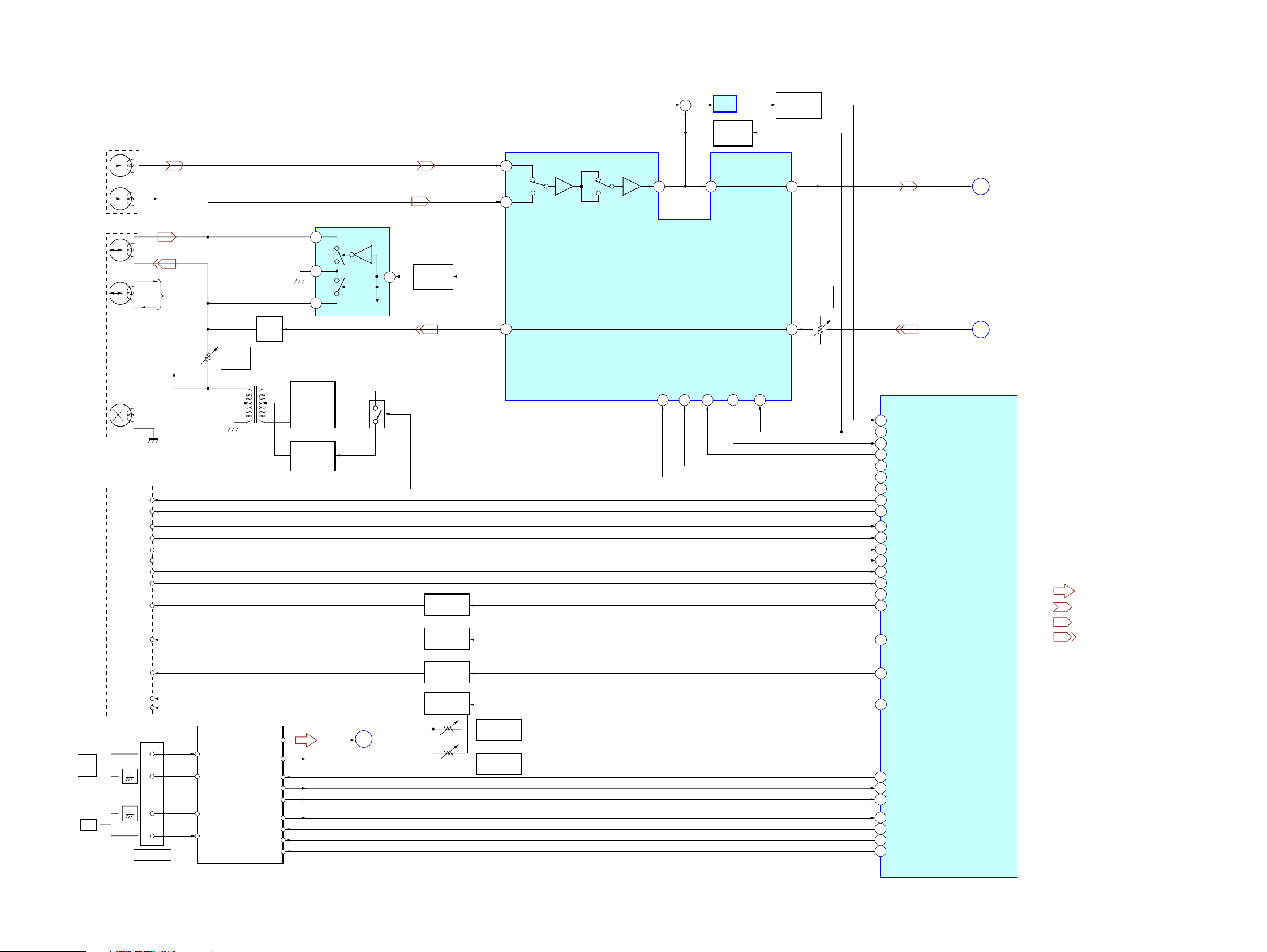
–TUNER/TAPE DECK SECTION –
DECK-A
R-CH
HCD-XGR90AV
IC341
+
HPF
MUTE
Q344,345
AMS DETECT
Q341-343
PB
HEAD
REC/PB
HEAD
ERASE
HEAD
FM
75Ω
AM
DECK-B
TC BLOCK
REC(REW)
REC(FWD)
B-PHOTO
A-PHOTO
B-MODE
A-MODE
B-HALF
A-HALF
A-SOL
B-SOL
CAP M+
MOTOR-L
MOTOR-H
CN371
ANTENNA
R-CH
R-CH
R-CH
C322,L321
RV321
REC
BIAS(L)
T331
FM/AM TUNER UNIT
ST-LOUT
FM ANT
FM ANT
AM ANT
AM ANT
ST-ROUT
ST-MUTE
STEREO
TUNED
OUT(ST-DIN)
IN(ST-DOUT)
ST-CLK
BIAS
TRAP
ST-CE
1
2
3
BIAS OSC
Q331,332
RIPPLE
FILTER
Q333
R-CH
ST-MUTE
STEREO
TUNED
ST-DIN
ST-DOUT
ST-CLK
ST-CE
REC/PB SWITCH
IC321
R-CH
TC A+10
ST-L
D
4
Q334,335
(Page 24)
SWITCH
Q321,322
Q383,384
A TRIG
DRIVE
Q381,382
B TRIG
DRIVE
Q385,386
CAP MOTOR
DRIVE
Q387,388
CAP MOTOR
SPEED CONT
RV391
RV392
32
34
21
RV931
TAPE SPEED
LOW
RV932
TAPE SPEED
HIGH
A
B
REC-OUT
70
120
DECK A/B SELECT
PB/REC EQUALIZER AMP
IC301
28 27 26
A/B
NORM/HIGH
13 12 11 15 14
ALC ON/OFF
PB-OUT1
ALC1
REC MUTE ON/OFF
MUTE ON/OFF
PB-L
RV351
REC(L)
LEVEL
23
(CD MECHANISM CONTROL)
REC-L
SYSTEM CONTROL
B
C
(Page 24)
(Page 24)
IC501(2/4)
53
AMS-IN
58
TC-MUTE
61
REC-MUTE
68
ALC
66
EQ-H/N
67
PB-A/B
BIAS
65
REC-B
50
REC-A
46
90
B-SHUT
A-SHUT
89
57
B-PLAY SW
56
A-PLAY SW
B-HALF
91
A-HALF
70
69
TC-RELAY
51
A-TRIG
52
B-TRIG
CAPM-CTRL
55
CAPM-H/L
54
ST-MUTE
21
STEREO
2
TUNED
3
ST-DIN
25
ST-DOUT
23
27
ST-CLK
ST-CE
22
• R-ch is omitted due to same as L-ch.
• SIGNAL PATH
: TUNER (FM/AM)
: PLAYBACK (DECK A)
: PLAYBACK (DECK B)
: RECORD
2323
Page 24
HCD-XGR90AV
– MAIN SECTION –
GAME
INPUT
DVD
INPUT
DVD
INPUT
(Page 25)
(Page 22)
(Page 23)
(Page 23)
PHONO
IN
MD IN
AUDIO
VIDEO
VIDEO
VIDEO OUT
FRONT
REAR
CENTER
SUB WOOFER OUT
E
A
B
D
L
R
L
R
L
R
L
R
L
R
DISTORTION
J802
GUITAR
J801
MIX MIC
CD-L
PB-L
ST-L
J701 (1/2)
J804
J721
J711
R-CH
R-CH
R-CH
R-CH
R-CH
DISTORTION
ON/OFF SWITCH
Q880 – 883
PHONO
EQ AMP
IC601
IN4 A
8
IN3
6
IN2
4
IN1
1
10
27
26
77
76
VD-OUT
(75Ω)
SL-IN
C-IN
MUTE
IC850 (1/2)
VIDEO INPUT
SELECT
IC191
6db
+
VCA
(L-R)
(L+R)
CONTROL
CENTER
MODE
GUITAR AMP
IC853
GUITAR AMP
IC852
MIC AMP
A+10V
B
C
A/D, D/A
LOGIC
RV601
GUITAR LEVEL
2
3
5
3
2
1
2
1
RV602
MIC LEVEL
+5V
REG
Q611
PRO-LOGIC
4240
SL
11
C
SRSW-IN
IC850 (2/2)
SOUND
CONTROL
IC201
+
MIC AMP
L-IN
10
45
161579
C
SR
FUNCTION SELECT
SWITCH
IC181
X0
12
X1
14
X2
15
X3
11
16
VDD
VSS
8
AB
10 9
Q181
172
L
SL
VOL
VOL
VOL
MIC OUT
X
13
Q182
DATA
LT-IN
VOL OUT SL
VOL OUT C
VR SW IN
1
VOL OUT SW
REQ
2
SCK
REC-L
R-CH
FAN MOTOR
B+
FAN MOTOR
DRIVE
Q961, 962
FRONT SPEAKER
SURROUND SPEAKER
R-CH
–1
–2
MUTE
Q805,855
RY401
RY403
MUTE
Q701
R-CH
NC
BB-B1
17
SWOUT
24
OUT1
18
Q112
Q165,166
R-CH
OVER LOAD
DETECT SWITCH
Q437
RELAY DRIVE
RELAY DRIVE
RELAY DRIVE
D803
R-CHR-CH
DELAY
Q833
Q401, 402
Q404, 406
Q403, 407
R-CH
2
8
X-IN
80
81
94
97
1
Q802,803
LEVEL SHIFT
82
83
86
11
10
13
15
88
87
85
95
MIC
RECB1
SURROUND OR
DPL BUFFER
X501
32.768KHz
X502
16MHz
MUTE
Q281
MUTE
Q271
R-CH
MUTE
Q114
-VEE
D811
MUTE
Q115
MUTE
Q731
C
A
B
C
A
B
+
TC
+10V
LEVEL
SHIFT
Q804, 807, 808
MID/
BASS &
TREBLE
R-CH
L+R
19
POWER AMP
18 11
IC801
12
STANDBY SWITCH
Q803, 804, 834
STANDBY
SWITCH
Q103, 104
16
POWER AMP
10 5
IC101(1/2)
POWER AMP
14 6
IC101(2/2)
F OUT2
R-CH
14 15
SPEANA
TH831
+
R-CH
COMMAND
(Page 25)
F
TEMPERATURE
DETECT SWITCH
Q831, 832
OVER LOAD
DETECT
Q801, 851
DC DETECT
SWITCH
Q433, 434
R-CH
VL
IN1
INPUT SELECT SWITCH,
GRAPHIC EQUALIZER CONTROL,
ELECTRICAL VOLUME
IC111
INC1
5
INB1
INPUT
4
INA1
3
IND1
6
INEX1
7
SUR1
42
FUNC-SEL0
71
FUNC-SEL1
72
REC/PB/PASS
59
NR-ON/OFF
60
VIDEO-MUTE
76
SYSTEM CONTROLLER
(CD MECHANISM CONTROL)
24
22
23
74
9
3
80
17
77
78
79
PL-LAT
PL-DAT
PL-CLK
SELECT
SWITCH
R-CH
AUDIO-OUT
LINE-MUTE
IC501 (3/4)
FRONT-RELAY
REAR-RELAY
+
+
EQIC-DAT
EQIC-CLK
DBFB-H/L
SW-MODE
STK-MUTE
HP-MUTE
XC-OUT
XC-IN
X-OUT
PROTECT
HP-IN
VOLUME
CONTROL
OVER LOAD
DETECT
Q101, 151
+
CPU
INTERFACE
DATA
CLK
BB-A1
22 1621
Q113 Q111
Q169,170 Q167,168
D401
OVER LOAD
DETECT SWITCH
Q432
PROTECT SWITCH
Q439
D410
Q805,806
LEVEL SHIFT
+
PROTECT SWITCH
Q431
RY402
R-CH
R-CH
(Page 23)
C
L
MD OUT
R
J701 (2/2)
M901
(FAN)
M
TM401
IMPEDANCE
USE 6 – 16Ω
+
L
–
+
R
–
J803
PHONES
• R-ch is omitted due to same as L-ch.
• SIGNAL PATH
: TUNER (FM/AM)
: CD PLAY
: TAPE PLAY
: RECORD
: MIC INPUT
TM402
IMPEDANCE
USE 8 – 16Ω
+
L
–
+
REAR
R
–
+
–
CENTER
J731
SUB WOOFER OUT
2424
Page 25

– DISPLAY/KEY CONTROL/POWER SUPPLY SECTION –
HCD-XGR90AV
VF
GRID DRIVE
Q608,609
FL601
FLUORESCENT INDICATOR TUBE
GRID DRIVE
Q606,Q607
S611,612,S741-751
S613-618,S801-809
S601-605,S701-711
S606-610,S752-755
S713-722,S724,S725
S763
AMS
.>
(JOG DIAL)
S700
VOLUME
ROTARY
ENCODER
S763
ROTARY
ENCODER
S700
FLUORESCENT INDICATOR TUBE DRIVER,
KEY CONTROL
IC601
70
BPF-F02
BPF-F03
71
72
LED LATCH
XOUT
X601
4MHz
EVER +3.9V
BPF-F04
BPF-F05
BPF-F06
ALL BAND
DIST
LED SELB
LED SELA
LED DAT
LED SCK
RESET
I2C-DATA
I2C-CLK
D-SW
XIN
73
74
75
53
55
80
78
76
79
77 41
60
61
52
43,44
18 – 21,24 – 41
SEG-1 – SEG-25
1
GR-16
8
GR-9
10,9,7-2
16,14 – 12
GR9-GR15
GR-2 ,GR-4-GR8
15
GR-3
17
GR-1
64 – 69
KEY 0 – KEY 5
59
JOG A
58
JOG B
VOL A
57
56
VOL B
82 83
NFF02
16
INF03
15
NFF04
14
INF05
13
F06
12
REC
LEVEL
11
DATA
16
17
CLK
18
STB
S746
LID (CD)
OPEN/CLOSE
RESET SIGNAL
GENERATOR
IC801
BAND-PASS FILTER
DET
DET
LED DRIVER
IC701
31
IC602
B.P.F.
P1 – P21
20-29,1-7,9-12
LED
DRIVE
Q601
D602 S619
POWER
SAVE
REMOTE CONTROL
RECEIVER
IC603
LINE
REC IN
RESET
SWITCH
Q801
(Page 24)
IN
4
6
B+ SWITCH
Q901-904
D701-717
D719,722
D700
S620
ON/OFF
1
(Page 24)
F
SPEANA
SYSTEM CONTROLLER
CD MECHANISM
IC501 (4/4)
OTM-RESET
30
IIC-DATA
29
IIC-CLK
LED-STBY
75
KEY-POWER
74
KEY-ECO
73
SIRCS
4
20
AC-CUT
RESET
12
E
DISTORTION
B+ SWITCH
Q602-605
CONTROL
CD-POWER
STBY-RELAY
D603-613
D801-806
38
84
LED
+3.9V
Q922
(CD TRAY SECTION B+)
(CD SENSOR SECTION B+)
(FM/AM TUNER UNIT B+)
(TC MOTOR SECTION B+)
(CD MOTOR SECTION B+)
CD A+5V (SW) ,
CD D+5V (SW)
CD MECHANISM
DECK SECTION
B+
+5V (LED)
(PANEL SECTION B+)
D+5V (UNSW)
D+5V (SW)
D+3.9V
LED
3.9V
–VEE
A+10V
ST +10V
TC+10V
FAN MOTOR B+
TC M+9V
CD M+7V
EVER +3.9V
SYSTEM CONTROLLER (IC501) ,
FL DRIVER (IC601) B+
POWER AMP (IC102,IC801),
PROTECT CIRCUIT
–35V
FL DRIVER (IC601)
B–
B+ SWITCH
Q921
D911-913
TO FLUORESCENT
INDICATOR TUBE
(FL601)
–35V
REGULATOR
Q903, 908
+5V
REGULATOR
IC921
+3.9V
REGULATOR
IC922
+10V
REGULATOR
IC931
+12V
REGULATOR
IC961
+12V
REGULATOR
IC911
+5V
REGULATOR
IC901
VF
VF
+VL
–VL
+VH
–VH
+10
-10
+15
RECT
D902 – 905
RECT
D832
RECT
D831
RECT
D841 – 844
RECT
D833 – 836
TRANSFORMER
TRANSFORMER
F963
F964
F961
F962
SUB POWER
T901
POWER
T951
VOLTAGE
SELECTOR
S901
AUS
E
RY901
POWER ON/OFF
RELAY DRIVE
Q901
AC IN
2525
Page 26

HCD-XGR90AV
7-3.PRINTED WIRING BOARD – BD SECTION – • See page 21 for Circuit Boards Location.
1
2
BD BOARD
3 4 5
OPTICAL PICK-UP
BLOCK
OP ASSY(A-MAX.3)
A
R143
JW126
JW125
IC101
CN102
C112
JW138
JW144
JR101
R119
C172
R172
C167
C168
R171
C162
JW121
R182
C182
C159
JW136
R162
JW120
C195
C114
R183
R173
R158
JW118
JW119
JR103
JW122
JW123
R181
C181
C171
X101
R116
JW137
1-680-003-
R159
28
1
JW124
JR105
+
–
M101
SPINDLE
MOTOR
22
7
JW112
JW113
JW117
FB102
M102
FB101
SLED
MOTOR
M
IC102
R118
R117
C129
C191
C190
D101
M
+
21
8
C121
R190
C153
JW145
RN101
JW102
E
JR106
12
(12)
15
14
JW111
C198
JW116
7
8
C122
L101
Q102
–
JW115
1
2
C126
JW114
C127
CN101
C125
JW110
A
MAIN
BOARD
(Page 33)
• Semiconductor
Location
Ref. No. Location
D101 D-4
JR125
JR124
R144
R122
C131
JW131
JW134
C143
C196
C197
C193
1
30
JW130
C117
R198
JW141
JW140
JW139
C123
JR123
JW129
C124
JR122
R148
R149
JR102
C194
JW128
JR104
R104
C165
C111
C110
JW127
C145
R123
E
R124
R195
C116
B
C192
C184
JW133
R111
C
R194
C183
RV101
C104
R191
JW132
C133
R101
R120
15
16
C101
C130
R193
R196
R192
IC103
R102
C102
R114
C185
R103
C103
R147
JW135
D
C118
JW142
R109
R108
C108
JW143
Q101
R105
R131
R107
R106
C109
E
IC101 C-2
IC102 B-4
IC103 C-1
Q101 B-2
Q102 D-4
2626
Page 27

7-4. SCHEMATIC DIAGRAM – BD SECTION – • See page 48 for IC Pin Function.
C108
0.1
k
B
1
6
0
1
R
k
0
1
7
0
1
R
VSS
PCO
VDD
DOUT
AVDD3
LCH
RCH
T
O
K
M
A
S
S
C
T
S
A
R
Q
Y
Q
X
S
S
S
D
k
1
7
1
1
R
CN101
PWM3
PWM2
PWM1
DVDD
DOUT
DGND
AGND
ROUT
AVDD
LDON
SQSO
SQCK
SCOR
MGND
21P
LOUT
XRST
DATA
CLOK
SENS
R131
220
LRCK
PCMD
C191
BCK
EMPH
XVDD
XTAI
XTAO
XVSS
AVDD1
AOUT1
AIN1
LOUT1
AVSS1
AVSS2
LOUT2
AIN2
AOUT2
AVDD2
RMUT
LMUT
100
10V
5L
C162
C181
680p
R183
100
R116
10V
10
R173
22k
C171
680p
CH
CH
C182
100p
22k
R182
R181
C129
0.01
F
R190
220
C121
0.1
C190
F
1
F
FB101
0µH
FB102
0µH
C198
100
10V
5L
L101
4.7µH
XLT
+7V
RN101
100
R118
100
C122
10V
100
5L
C168
X101
33p
16.9344
CH
C112
C167
1
B
22p
CH
2.7k
R171
R172
C172
22k
22k
C125
0.1
F
R119
22k
22k
100p
CH
CH
C114
0.1
F
Q102
2SD1664
D101
UDZ-TE-17-3.9B
HCD-XGR90AV
R196
680
C183
C185
R194
F
10V
BALANCE
R101
1k
C101
3300p
B
C102
0.1
B
C126
0.1
C127
100
10V
RV101
F
5L
33k
R111
120k
C133
33p
R191
33k
RV101
R192
E-F
TP2
RFDC
R102
100k
47k
33k
R114
R193
160k
120k
R147
2.4k
R198
0
TP3
VC
C153
0.1
F
22000p
1µ
B
B
C110
3300p
B
B
p
0
R108
0
5
3.3k
1
9
0
1
C
FILI
FILO
CLTV
AVSS3
K
S
T
K
L
A
O
N
L
L
E
C
X
C
S
S
B
7
.4
0
H
4
C
2
1
C
p
0
0
1
M
1
1
1
1
9
0
C
1
R
BIAS
ASYI
RFAC
IC101
CXD3017Q
DIGITAL SERVO
DIGITAL SIGNAL
PROCESSOR
A
K
D
O
S
D
T
P
V
A
S
C195
0.1
F
ASYO
B
O
P
S
C123
0.01
R124
100k
R123
B
C165
0.1
F
R104
10k
IGEN
ADIO
AVSSO
AVDDO
K
F
K
N
C
G
C
O
F
L
U
P
X
W
X
X
C145
0.1
RFDC
FS
G
F
TE1
TE
CE
SE
FE
VC
XTSL
TES1
TEST
VSS
FRDR
FFDR
TRDR
TFDR
SRDR
SFDR
SSTP
MDP
LOCK
FOK
DFCT
MIRR
COUT
R
O
O
P
2
C
C
S
R105
1k
33k
C104
470p
R120
B
0.1
C194
C193
100
15k
C103
470p
B
R103
15k
FE1
SE1
CH
FE
FEI
TE
TE_BAL
CE
CEI
VCC
RFG
BST
VFC
RFC
VC
RFDCO
RFDCI
DC_OFST
C184
0.01µ B
IC103
CXA2581N
RF AMP
R195
RFAC
DVC
DVCC
SW
F
E
D
C
B
A
GND
AC_SUM
EQ_IN
PD
LD
IC102
BA5974FM-E2
MOTOR/CIL
DRIVE
220k
TP1
RFAC
C196
C192
0.1
F
C116
100
10V
C130
0.1
F
C131
C118
1000p
B
C117
100
10V
R122
100
100k
10V
SPD1
R162
100k
C197
0.1
B
0.1
F
Q101
2SB710-RTX
DRIVE
LD
R149
10
R148
10
C159
0.01
B
R159
27k
R158
R144
33k
C143
0.1
27k
R143
33k
F
1
2
1
2
D
D
D
D
T
T
F
F
CN102
16P
I1-6
VC
I5-10
VCC
PD2
GND
PD1
SW
PD
LD GND
LD
VCC
T-
F-
T+
F+
M102
SLED
MOTOR
M101
SPINDLE
MOTOR
OPTICAL
PICK-UP
BLOCK
(A-MAX.3)
2727
Page 28

HCD-XGR90AV
B
MAIN BOARD(2/3)
(Page 31)
4.8
4.8
4.8
4.8
LED DRIVE
TABLE MOTOR DRIVER
DISC TABLE SENSOR
TRAY
7-5.PRINTED WIRING BO ARD – MOTOR, LED SECTION – • See page 21 for Circuit Boards Location.
LED BOARD
SENSOR BOARD
7-6.SCHEMATIC DIAGRAM – MOTOR, LED SECTION –
MOTOR BOARD
B
MAIN BOARD
(Page 33)
2828
Page 29

HCD-XGR90AV
MIC/GUITAR BOARD
11
(12)
1-683-455-
J802
GUITAR
J801
MIX MIC
IC852
IC853
C881
1
8
1
8
IC850
C806
C818
R858
R887
JW813
JW817
Q880
R857
R873
JW824
JW818
FL801
C838
C837
C880
C884
R876
R879
R877
R874
Q884
Q883
JW812
R888
Q882
R885
R889
Q881
R883
R880
R882
R881
C882
JW822
R886
R872
JW823
JW814
JW819
JW805
JW820
JW806
C824
R884
C810
R867
C836
C801
R807
R809
R854
C804
C802
C813
R891
C814
R870
C815
R850
R855
C819
R856
R853
JW801
R878
JW816
C821
C805
R852
C817
C803
C822
CN812
C816
JW821
JW481
JW804
NO811
CLP804
NO802
(CHASSIS)
JW815
E
E
1
6
E
E
E
L
TC–A
BOARD
(Page 38)
E
MAIN
BOARD
(Page 33)
1
8
1
3
2
3 4
A
1
B
C
D
E
F
7-7.SCHEMATIC DIAGRAM – MIC/GUITAR SECTION –
ECHO/GUITAR-IN
ECHO/GUITAR-OUT
MIC-VR-OUT
MIC-VR-IN
DISTORTION
MIC-OUT
MIC_GND
GND
NO811
3P
+10V
CN812
CT-S
2SC2603
7
6P
R874
15k
R867
2.2k
C816
2.2
50V
R873
2.2k
C821
47/16
C837
10
50V
R878
1k
Q880
R881
47k
8
C880
2.2
50V
IC853(2/2)
NJM4558L
C824
2.2
50V
R880
6
5
47/16
IC853
GUITAR AMP
10k
C882
R855
10k
C822
47p
R882
47k
Q880-883
DISTORTION
ON/OFF SWITCH
IC853(1/2)
NJM4558L
1
R886
390k
R857
4.7k
C817
2.2
50V
IC850(2/2)
NJM4558L
7-8.PRINTED WIRING BOARD – MIC/GUITAR SECTION –
• See page 21 for Circuit Boards Location.
R876
1k
C838
R877
R852
100k
10
50V
330
C805
1000p
R879
1k
R872
2.2k
R887
10k
Q883
R885
10k
DTA124ESA
C810
IC850
MIC
AMP
3
2
4
R883
47k
680k
R856
C881
47p
R884
470
C884
R889
2.2
22k
50V
Q881
2SC2603
R850
1k
C819
47p
6
7
8
C818
47p
5
220p
R854
Q882
DTC124ESA
47k
R888
1k
IC850(1/2)
NJM4558L
1
4
IC852(1/2)
NJM4558L
7
R853
1k
C803
50V
5
6
8
C806
47p
3
2
1
R870
220k
IC852(2/2)
NJM4558L
1
4
C804
0.47
50V
R809
1k
R807
10k
Q884
2SC2785
C814
47p
IC852
GUITAR AMP
C813
R869
0.022
68k
2
C815
47p
C801
10000p
C802
R891
1M
J802
NO802
(CHASSIS)
GUITAR
J801
MIX MIC
47p
FL801
C836
10000p
3
• Semiconductor
Location
Ref. No. Location
IC850 C-3
IC852 C-1
IC853 D-2
Q880 E-2
Q881 F-1
Q882 E-2
Q883 F-2
Q884 D-3
2929
Page 30

HCD-XGR90AV
7-9.SCHEMATIC DIAGRAM – MAIN (1/3) SECTION –
PHONO IN
DVD INPUT
MD IN
MD OUT
VIDEO OUT
VIDEO
FRONT
REAR
CENTER
WOOFER
(CHASSIS)
J701
L
R
L
R
L
R
J721
1P/2P
J711
C701
220p
C751
220p
Q701
MUTE
Q751
75
IC601(1/2)
4558M
NJM
C603
100p
C653
100p
C704
10
50V
C711
220p
C761
220p
C712
220p
C762
220p
C713
220p
C763
220p
8
4
0.0015
IC601(2/2)
NJM4558M
R706
2.2k
C182
0.1
R756
2.2k
R722
C724
470p
R606
47k
C606
C656
0.0015
PET
R656
47k
7
R705
R755
39
R607
1
PET
R657
C183
0.1
C703
10
50V
10k
10k
3
2
R605
560k
C605
0.0047
PET
C655
0.0047
PET
R655
560k
6
5
0.1
C181
C754
10
50V
C722
1000
10V
C723
1
50
C714
10
50V
C764
1
50V
IC601
PHONO EQ AMP
R602
1k
R604
1k
R601
1k
C608
10
50V
6P
C772
0.1
C774
0.1
6P
L
R
L
R
C775
0.1
R603
47k
C602
100p
C604
2.2
C601
50V
330p
C651
330p
C654
2.2
50V
R653
47k
C652
100p
R654
1k
R652
1k
R651
1k
C658
10
50V
R707
680k
IC181
MC14052BF-
FUNCTION
SELECT
ITCH
SW
C771
0.1
R702
R701
100k
1k
R751
R752
1k
100k
R704
R703
100k
R753
1k
1k
JR723
2SC3623A
C702
220p
C752
220p
2SC3623A
MUTE
R754
100k
0
R724
10k
R723
R712
R711
10k
8.2k
R761
R762
8.2k
10k
R714
R713
10k
6.2k
R763
R764
6.2k
10k
R716
R715
10k
6.2k
R765
R766
6.2k
10k
C609
0.01
C607
0.033
MF
1k
R608
100k
R658
100k
C657
0.033
MF
1k
R757
680k
C753
10
C193
0.1
R609
220
C610
100
16V
701
JW
Q181,182
INVERTER
72
C
76
C611
47
16V
Q182
DTC124ESA
3
IN
D191
1SS355
R611
1k
R612
1k
R613
330
D-OUT
GND
JR191
V
IN4
0
C192
10
50V
C191
0.01
VCC
Q611
2SC2603
C613
47
16V
R614
C612
1k
0.01
R181
10k
R182
10k
Q181
DTC124ESA
71
50V
IC191
BA7615N
VIDEO INPUT SELECT
IN1
IN2
A
B
59
60
D192
1SS355
R133
4.7k
100
50V
10
50V
50V
50V
C133
10
10
C132
10
16V
C113
C112
C111
50V
50V
50V
10
10
10
C163
C162
C161
50V
50V
50V
10
10
10
C110
C115
C114
50V
50V
50V
10
10
10
C160
C165
C164
0.022
C116
0.022
C166
C118
10
R111
2.2k
0.022
C117
162
10k
R
0.022
C168
C167
50V
R161
2.2k
751
JW
10
50V
112
10k
R
C120
4700p
C119
0.047
C170
4700p
C171
C169
0.033
10
50V
10
LT-IN
RT-IN
L-OUT
AGND
R-OUT
VRSWIN
C-IN
SL-IN
SR-IN
SW
CN151
10P
TKC-D1
-IN
IC111
M61519FPD60G
INPUT SELECT
SWITCH,
GRAPHIC
EQ CONTROL,
ELECTRICAL
VOLUME
C121
50V
R132
C136
R113
1M
33k
10
50V
C122
0.33
MF
R135
0
80
C137
0.0022
C138
0.0022
81
R136
0
2
D
EO
.GND
.L-CH
V.GN
A
VID
V2.AU
V2.AU.R-CH
Q111
2SK1825
CN722
5P
S
Q112
R116
2SK1825
47k
R115
47k
C123
0.33
MF
R119
R120
680
220k
C135
C134
47
16V
0.01
Q116,164
MUTE
R169
680
C173
0.33
MF
C172
0.33
MF
R165
47k
R166
47k
Q161
2SK1825
S
R163
1M
EH-S
Q111,112,113
SWITCH
2SK1825
R137
0
C124
2.2
50V
R125
10k
R179
10k
C174
2.2
50V
R170
220k
Q161,162,163
Q167-170
S
Q113
SW
Q162
2SK1825
S
R177
Q114,115
MUTE
R122
2.2k
123
R
173
R
100k
R172
2.2k
R138
ITCH
AMP
1M
R117
220k
100k
0
S
2SC3623ATP
2SC3623ATP
R171
DTA124ESA
DTC124ESA
R731
10k
S
Q167
Q168
Q114
Q164
R124
R174
R134
R118
220k
10k
10k
R130
1M
1M
R129
1M
R127
220k
R121
680k
Q115
2SC3623ATP
R126
10k
R180
10k
Q116
2SC3623ATP
680k
Q165,166
AMP
Q165
DTA124ESA
Q166
2SC2603
R176
22k
R175
1M
7
9
Q169
DTA124ESA
Q170
DTC124ESA
78
79
R732
77
1k
C732
220p
R733
100k
C733
0.1
C776
0.1
C731
10
50V
R167
220k
R168
220k
Q163
2SK1825
R128
220k
94
Q731
2SC3623A
MUTE
R178
1M
R734
UTE
SW-M
TA-MUTE
AC-MUTE
UTE
RECOUT-M
L-CH SIG
GND
R-CH SIG
+10V
DBFB
SPE-SIG
MC1
MIC-SIG
ST-R
ST-L
CD-R
CD-L
PL A+10V
TCREC-R
TCPB-R
TCPB-L
TCREC-L
AU D+5V
CN152
10P
TKC-D1
TA-MUT
PL-DAT
PL-CLK
PL-LAT
D+5V
DGND
PL+10V
AGND
AGND
SW-OUT
J731
1P
1k
SUB WOOFER OUT
3030
Page 31
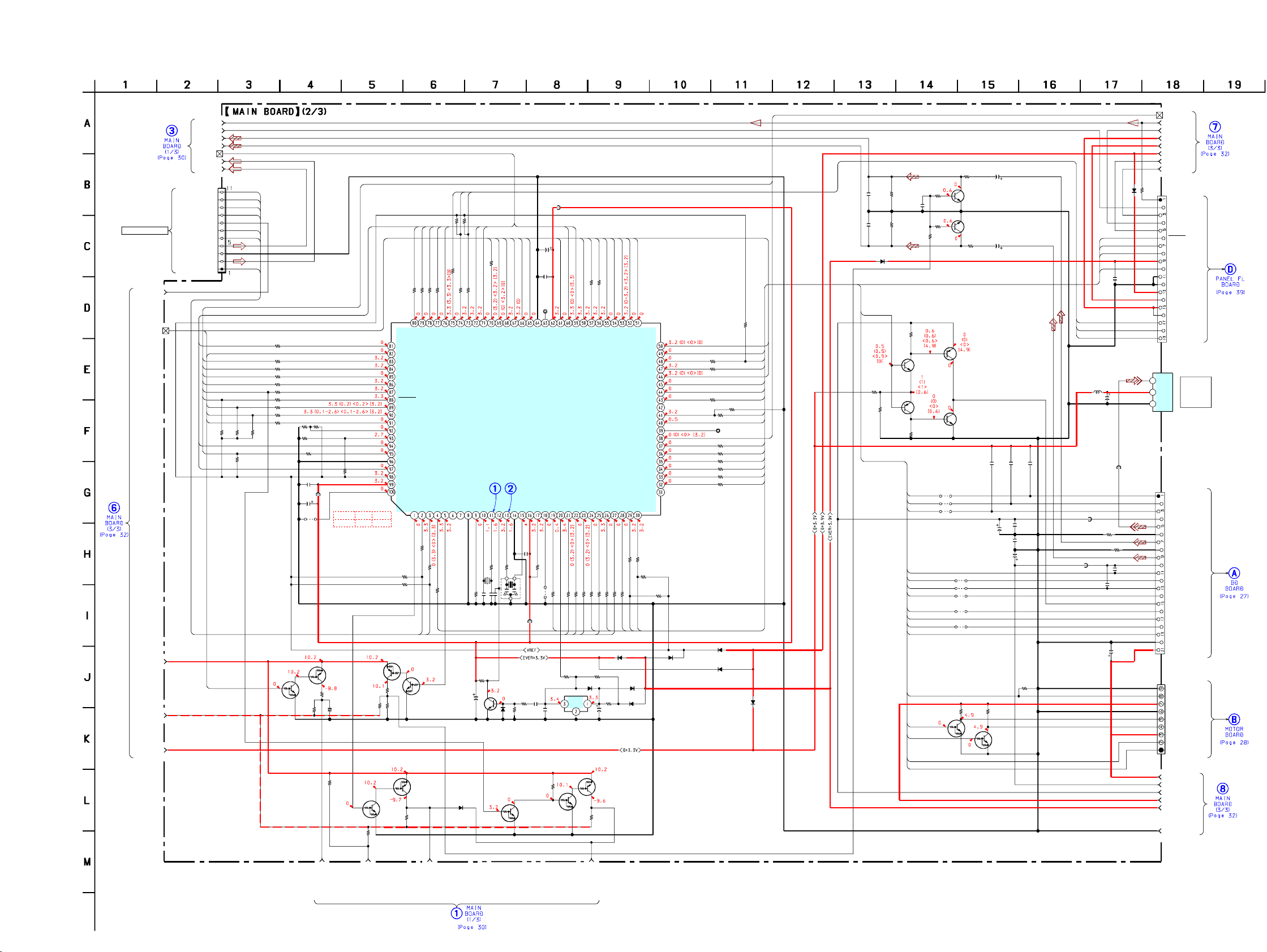
7-10.SCHEMATIC DIAGRAM – MAIN(2/3) SECTION – • See page 50 for IC Pin Function.
MIC-SIG
SPE-SIG
CD-L
CD-R
MC1
ST-R
ST-L
CN441
11P
TUNER PACK
ST +10V
TC+10V
D+3.3V
ST-CLK
O
U
T(ST-DIN
)
IN
(ST-D
OU
T)
ST-CE
ST+10V
TUNED
STEREO
S
T-LO
U
T
A-GND
ST-R
O
U
T
ST-MUTE
MC3
81
82
83
84
85
86
87
88
89
90
91
94
95
97
82
-VEE
R582
27
25
23
22
3
2
21
R581
100
R583
100
R584
100
R585
100
R586
100
R587
100
R588
100
R589
100
R590
100
R591
R598
LEVEL
47k
Q802,803
R596
SHIFT
DTC124ESA
Q802
R593
330
*1
R595
C598
FB599
47
R808
100k
R597
10k
47k
R599
10k
100
0µH
C599
JW600
16V
R807
4.7k
R592
100
R594
*1
R594
R596
Q803
DTA124ESA
C806
2.2
50V
B.P.
R813
10k
DTC124ESA
Q806
R812
*1
AUS
E
4.7k
1k
0
4.7k
DTA124ESA
R814
22k
815
816
R
R
100k
R810
100k
3.3k
LEVEL
Q805,806
0.1
0
EQIC
-CLK
LINE-MUTE
STK-MUTE
STBY-RELAY
REAR-RELAY
HP-MUTE
FRONT-RELAY
PROTECT
A-SHUT
B-SHUT
B-HALF
MODEL-IN
DEST-IN
DBFB-H/L
HP-IN
AVSS
SW-MODE
VREF
AVCC
RDS-DATA
R501
10k
R505
10k
Q810
22k
SHIFT
79
80
100
100
579
R580
R
IC-DAT
EQ
T
UDIO
-OU
A
100
R502
2
DTC124ESA
Q809,810
LEVEL
Q805
DTA124ESA
100
578
R
PL-CLK
EO
STER
Q809
78
100
503
R
3
SHIFT
AT
PL-D
ED
TUN
100
R577
77
4
R572
15k
PL-LAT
SIRCS
76
100
R575
TE
U
VIDEO-M
UTE
CD-M
100
R504
1SS355TE-1
73
74
75
R571
15k
71
-STBY
LED
100
R574
D811
100
573
R
ER
W
KEY-PO
C804
1000
6.3
72
KEY-ECO
BYTE
10k
509
R
RESET
NC-SEL1
FU
S
CNVS
32.768kHz
501
X
C510
18p
R806
10k
2SC2603
70
100
R570
NC-SEL0
FU
C-IN
X
330k
R511
C511
22p
Q801
SWITCH
-HALF
A
C-OUT
X
68
69
TC-RELAY
RESET
0.1
C512
X502
16MHz
1SS355TE-1
Q808
DTC124ESA
ALC
UT
X-O
R805
47k
65
66
67
PB-A/B
EQ-H/N
IC501
M30620MCN-A01FP
SYSTEM
CONTROL
X-IN
VSS
0.1
C516
0
513
R
FB516
0µH
R804
47k
0.1
D808
BIAS
VCC
C803
0.1
MF
C802
VSS
I
M
N
10k
517
R
MF
C563
47
16V
C562
0.1
TP563
SOFT-TEST
S-INT
RD
100
518
JW
R519
19
R811
10k
Q807
DTC124ESA
FB562
0µH
VCC
R
SCO
0
6
61
E
FF
UT
/O
-M
-ON
EC
R
NR
TE
T
U
-CU
-M
ST
AC
00
1
521
R
1
2
R803
4.7k
IC801
M62703SL
RESET SIGNAL
GENERATOR
Q804
DTA124ESA
HCD-XGR90AV
MC2
IC
M
VF1
LED 3.9V
BPF+10V
D 3.9V
VF2
VFDP
R401
Q454
100
2SC3623A
2SC3623A
R403
100
Q453
Q401
Q402
R414
C403
10
50V
Q401,402
MUTE
C404
10
50V
73
74
75
L451
100
C413
C412
4700p
C407
0.1
C408
1000
6.3V
Q412
DTC124ESA
C411
0.47
C401
0.1
R412
15k
FB403
FB402
0µH
0µH
0.01
C402
1000
6.3V
10k
R405
C405
R402
100p
33k
C406
R404
100p
EC10DS2-TE
40
R451
10k
R452
10k
D810
Q452
2SA1175-HFE
R453
33k
10k
R454
10k
59
SS
/PA
EC/PB
R
ST-CE
00
1
522
R
22
D807
58
100
3
R52
3
2
TE
U
-M
TC
UT
O
ST-D
100
4
52
R
24
R802
56
57
100
100
556
R557
R
W
B-PLAY S
3
M
W
-P
BU
25
1SS355TE-1
R809
100k
55
L
W
-CTR
APM
A-PLAY S
C
2
M
W
IN
-P
ST-D
BU
100
100
526
525
R
R
26
D802
4.7k
R801
220
C801
10
Q804,808,809
LEVEL
50
54
100
R527
27
SHIFT
/L
-H
PM
CA
ST-CLK
52
53
G
S-IN
-TR
B
AM
BU UP/DW SW
1
M
W
-CLK
BU-P
IIC
100
R529
100k
528
R
29
28
1SS355
D805
1SS355TE-1
D806
1SS355TE-1
51
G
-TR
A
REC-B
TBL-SENS
LED-DISC
REC-A
MTR-CTRL2
MTR-CTRL1
XRST
OTM-RESET
HOLD
CLK-OUT
CD-POWER
CD-CLK
CD-DATA
SENS
SQ-CLK
SQ-DATA
-DATA
IIC
100
R531
530
R
10k
30
549
10k
R
50
R541
R537
R536
R535
R534
R533
R532
49
100
48
100
47
46
45
44
100
43
47k
R540
41
100
40
38
37
100
36
100
35
100
34
100
33
100
32
100
2
S
809
D
EC10D
R548
R547
R543
TP539
XLT
R516
10k
D803
D801
1SS355
1SS355
D804
1SS355
C414
0.1
24
26
28
43
35
36
37
32
34
33
19
49
45
44
47
48
Q451
2SC2603
JW401
JW402
JW403
DTC124ESA
10k
R406
10k
R410
4.7k
Q451-454
BUFFER
Q411
JW406
JW407
JW408
JW409
JW410
Q411,412
INVERTER
R413
10k
2SA1175-HFE
2SC2603
S355
1S
31
D4
41
30
29
4
C431
0.1
C452
47
µH
16V
FB404
0µH
R407
0
R408
0
1500p
C415
1500p
C416
C410
470
10V
R431
100k
CN411
CT-S
CN431
19P
FFC-S
MIC-SIG
SPEANA
VFDP
VF
VF
RESET
IIC DATA
IIC CLK
EVER 3.3V
SIRCS
PANEL GND
PANEL GND
GC 3.3V
+10V
LED 3.9V
LED 3.9V
KEY ECO
KEY POWER
LED STBY
IC451
TOTX141
D.OUT
3.3V
D.GND
9P
CN401
21P
PWM3
PWM2
PWM1
DSP+5V(SW)
D-0UT
D-GND
L-CH
A-GND
R-CH
RF+5V(SW)
X-RST
CD-DATA
X-LAT
CD-CLK
LD-ON
SQ-DATA
SENS
SQ-CLK
SCOR
M-GND
M+7V(UNSW)
D.GND
TRAY.SENS
+5V
M.GND
TBL.L
TBL.R
+7V
LED
UP.SW
M +7V
CD A+5V SW
CD D+5V SW
D+5V UNSW
EVER+3.9V
GND
CD
DIGITAL
OUT
OPTICAL
TE
U
-M
TA
UTE
AC-M
UTE
T-M
ECOU
R
TE
U
-M
SW
3131
Page 32

HCD-XGR90AV
7-11. SCHEMATIC DIAGRAM – MAIN (3/3) SECTION –
IC341
HPF
44,345
TAPE A
HEAD
TAPE B
HEAD
PL A+10V
TCREC-R
TCREC-L
TCPB-L
TCPB-R
FOR
CHECK
L-REC
R-REC
E-HOT
Q3
Q345
R318
TC124ESA
D
10k
Q344
DTC124ESA
CN301
3P
OLEX
M
CN311
EH
3P
L-PB
GND
R-PB
CN321
EH
8P
L-PB
GND
R-PB
GND
GND
REC BIAS
C331
0.01
100V
PET
341
R
UTE
M
R319
100k
R342
1k
(L)
C326
27p
BIAS TRANS
1k
RV321
220k
Q331,332
BIAS
OSC
T331
IC341(2/2)
4558M
JM
N
5
C342
0.1
C341
470
10V
6
R320
2.2k
C350
1
R321
10k
REC BIAS
RV322
(R)
220k
C327
27p
R331
5.6
1/4W
FR
C332
2.2
50V
C343
8
0.022
PET
7
R343
1M
349
C
22p
R345
10k
C346
2.2
50V
C358
390p
C308
390p
C359
390p
C309
390p
IC321
µPC1330H
C321
10
50V
Q331
2SC2001
R332
5.6
1/4W
FR
D
GN
IC341(1/2)
NJM4558M
R346
10k
C
0.022
4
2
3
344
R347
PET
10k
R344
10k
IC301
HA12237F
A/B
DECK
SELECT
P
REC/PB EQ AM
C357
47
16V
C312
10
50V
TP304
C307
47
16V
IC321
PB-REC SW
Q321,322
ITCH
SW
C322
120p
PET
R328
12k
L321
H
27m
C324
330p
L322
C325
H
27m
330p
R329
12k
C323
120p
PET
C333
0.015
PET
Q332
2SC2001
C347
10
50V
1
R348
10k
C352
10
50V
C345
R352
2.2
4.7k
50V
353
JR
0
ITCH
Q322
DTA124ESA
R326
10k
R327
10k
Q333
RIPPLE
FILTER
PET
18k
6800p
R333
C334
JR303
C351
0.01
PET
C301
0.01
PET
0
C302
10
DTC124ESA
18k
R334
JR351
353
C
0.1
F
M
R351
3.3k
R301
3.3k
C303
0.1
F
M
R302
4.7k
50V
Q321
R324
2.2k
C328
0.01
B
C329
0.01
B
R325
2.2k
Q333
2SD1387
PET
PET
0.018
6800p
C336
C335
C337
10
50V
338
R
22k
R349
4.7k
Q341
2SC2603
358
R
10k
RV351
22k
0
C355
1
50V
C354
10
50V
TP351
TP301
C304
10
50V
C305
0.1
50V
0
R304
JR301
R336
2.2k
R337
3.3k
R305
47k
2.2k
R330
22k
C338
47
16V
Q334
DTC124ESA
R340
10k
REC LEVEL
R354
2.2k
TP352
TP302
Q335
2SB1116
339
R
10k
350
R
10k
Q341-343
S DE
AM
Q343
DTC124ESA
Q342
DTC124ESA
C348
22
50V
(L)
355
R
47k
C356
2.2
50V
P303
T
R308
22k
C310
R309
10
1M
50V
C306
REC LEVEL
2.2
50V
(R)
R310
RV301
22k
10k
52
R381
Q381
2SB1116
0.0047
1SS355
680
C381
R383
2.2k
R382
2.2k
Q382
D382
DTC124ESA
Q381,382
B TRIG
DRIVE
65
69
D381
R335
22k
Q334,335
ITCH
SW
C311
100
16V
Q383,384
A TRIG
DRIVE
1SS355
TECT
2SB1116
C382
0.0047
53
C313
10
50V
R311
4.7k
Q383
R385
2.2k
MOTOR-L
10k
R372
56
56
MOTOR-H
61
58
67
66
68
R384
680
R386
2.2k
Q384
DTC124ESA
A-SOL
A-MODE
L301
µH
100
51
CAP M
10k
R371
70
70
89
M-GND
A-HALF
A-PHOTO
MECHANISM DECK
Q385,386
2SB1068
CAPM+
TAPE
DRIVE
R388
3.3k
OTOR
Q385
10k
R377
46
46
REC(FWD)
90
B-PHOTO
R387
47k
R389
3.3k
R390
3.3k
Q386
DTC124ESA
10k
10k
R374
R375
57
91
57
91
B-SOL
B-HALF
B-MODE
10k
R378
50
50
REC(REW)
SW-GND
55
CN371
FFC-S
15P
D+3.3V
ST +10V
TC+10V
-VEE
TAPE SPEED
(NORM
RV391
4.7k
RV392
TAPE SPEED
C3
M
R922
0
C925
0.1
µPC7812AHF
+12V REGULATOR
C962
0.1
INVERTER
CN901
IC961
Q921
2SB1375
903
C
470
16V
13P
C923
1000
6.3V
R961
4.7k
922
Q
DTC124ESA
INVERTER
C924
47
16V
38
C913
47
16V
D913
EC10DS2
D912
EC10DS2
D911
EC10DS2
C912
470
10V
54
R393
AL)
R391
2.7k
R392
2.2k
2.2k
(HIGH)
10k
R394
Q387
220k
DTC124ESA
Q387,388
OTOR
CAP M
SPEED CONT
Q388
2SK1825
µPC3504AH
+3.9V REGULATOR
C926
470
6.3V
IC911
TA8662N
+12V REGULATOR
IC922
F
C911
100
25V
85
+10V R
PL-RELAY
M
FAN.DET
JW
C963
16V
IC931
5F7810L
EGULATO
87
F-RELAY
47
962
R962
IC921
µPC7805AHF
REGU
+5V
R
DBFB
Q961
2SC2603-EF
22k
LCH-IN
LATOR
A.GND
FAN SW
C
0.1
C901
4700
RCH-IN
Q961,962
902
25V
POWER GND
ITCH
R963
2.2k
C921
2200
16V
C922
0.1
NC
10VGND
2SB1116A-L
Q962
15VGND
UNREG+10V
C961
0.1
UNREG+15V
83
88
+10V
D.GND
VF(-35V)
PROTECT
EVER+3.9V
STK POWER
CN961
3P
EH-L
FAN+
FAN-
FAN+
84
95
86
CN902
13P
VF
VF
NC
-VEE
HP.SW
POWER
HP MUTE
901
M
CD D+5V SW
CD A+5V SW
D+5V UN
+7V
M
EVER+3.9V
AU D+
(CHASSIS)
CN903
3P
CT-S
MIC GND
IC
M
+10V
L-CH SIG
GND
R-CH SIG
DBFB
+10V
BPF+10V
IC
M
D 3.9V
LED 3.9V
VFDP
VF2
VF1
C2
M
SW
5V
EP901
3232
Page 33

7-12.PRINTED WIRING BOARD – MAIN SECTION – • See page 21 for Circuit Boards Location.
HCD-XGR90AV
A
B
C
D
E
F
G
H
I
PA
BOARD
(Page 40)
G
PA
BOARD
(Page 40)
F
(CHASSIS)
1
MAIN BOARD
CLP2
JW
JW
JW
EP901
L451
2
00
JW
JW209
255
256
202
JW
JW208
CN901
JW
JW962
N
G
D
C
O
1
203
JW207
CN902
257
C452
D
D
O
P
2
3 4 5 6 7
8
9 10 11
TAPE
Q383
E
Q381
E
C311
R321
C381
R383
R
R338
C601
C
350
Q
C354
JR
C331
C612
651
JW535
431
CN
R
E
342
JW400
C310
JR353
R352
JR351
JW
17
C611
613
R
C613
R614
R
C
382
Q
20
21
43
601
658
JW7
R349
343
JW585
D
R
JW24
R309
C604
R348
IC341
C
339
C305
C353
C351
C605
604
R
C608
651
R
PANEL FL
BOARD
(Page 38)
1
43
R
347
C
4
5
342
343
R
C349
JW
JW341
C345
RV301
C306
R310
IC301
11 10
30 31
R351
C357
C352
JW30
JW46
548
JW
549
JW
547
JW
546
JW
545
JW
544
JW
JW
JW
Q611
E
R611
R612
608
R
C603
602
R
16
JR
C602
JW
653
R
C652
652
R
Q731
E
C731
2
1
R
1
8
341
R
554
R320
C350
R
R344
C303
1
40
JW28
C312
C359
JW586
552
JW
551
JW
550
JW
543
JW
542
JW
541
540
539
JW
538
JW
606
R
C
R
IC601
4
R603
5
536
R
R
653
C
654
R
733
R
1-683-458-
346
Q
R3
345
JW27
606
605
656
655
R347
C
342
R
344
Q
19
C304
R301
C301
JW25
C309
CN903
2
10
607
R
1
34
JW
345
CN441
1
JW
8
R
1
JW
603
318
R
JW23
JR
C308
C358
11
556
C607
C609
657
C
C346
JW
C610
344
602
R
R
JR301
303
3
R302
CN311
537
R609
C343
JR
305
304
C3
C
C656
307
R
C654
E
26
02
1
3
658
C657
C655
TAPE A
HEAD
MIC/GUITAR
BOARD
(Page 29)
E
TUNER
PACK
TAPE B
HEAD
S
PROLOGIC
BOARD
(Page 44)
12
• Semiconductor
Location
Ref. No. Location Ref. No. Location
D191 G-6
D192 H-6
D381 B-9
D382 B-9
D431 A-7
D801 B-6
D802 B-5
D803 B-6
D804 B-6
D805 B-5
D806 B-5
D807 B-5
D808 B-6
D809 B-7
D810 B-7
D811 B-5
D911 C-3
D912 C-3
D913 C-3
IC111 F-4
IC181 H-7
IC191 H-6
IC301 C-10
IC321 E-9
IC341 B-10
IC451 H-2
IC501 B-7
IC601 H-10
IC801 B-5
IC911 C-3
IC921 D-3
IC922 E-3
IC931 F-3
IC961 H-2
Q111 F-3
Q112 F-3
Q113 F-3
Q114 G-2
Q115 G-2
Q116 G-2
Q161 G-3
Q162 G-2
Q163 G-3
Q164 G-2
Q165 G-2
Q166 G-2
Q167 H-3
Q168 H-2
Q169 H-3
Q170 H-2
Q181 H-6
Q182 H-6
Q321 E-9
Q322 E-9
Q331 F-9
Q332 F-9
Q333 F-9
Q334 F-8
Q335 E-8
Q341 B-9
Q342 C-10
Q343 B-10
Q344 B-10
Q345 B-10
Q381 B-9
Q382 B-8
Q383 B-9
Q384 B-8
Q385 B-9
Q386 B-9
Q387 B-8
Q388 B-8
Q401 B-3
Q402 B-4
Q411 B-2
Q412 B-2
Q451 D-4
Q452 D-4
Q453 D-3
Q454 D-4
Q611 G-10
Q701 H-6
Q731 H-10
Q751 H-7
Q801 B-6
Q802 B-6
Q803 B-5
Q804 B-5
Q805 B-5
Q806 B-5
Q807 B-5
Q808 B-5
Q809 B-5
Q810 B-5
Q921 C-3
Q922 D-4
Q961 H-3
Q962 H-3
E
15
73
72
JW
RV322
R3
JW557
14
JW3
71
L322
C322
Q
C333
C335
JW523
JW
734
R
OUT
333
525
38
R
88
JW
CN
R
JW524
JW39
JW
159
301
325
JW47
E
JW53
MECHANISM
R390
9
JW
R386
8
JW
JW
R372
JR24
R371
JW36
JW37
JW38
40
JW
41
JW
160
34
JW
35
JW
3
C323
JW558
JW49
C327
RV321
JW
Q331
E
R333
E
R334
R332
Q332
526
JW
JW527
JR30
11
JW
4
R377
JW
51
JR12
C
1
JW45
Q
DECK
R385
2
R3
JW
R378
JW32
JW31
L301
6
35
48
JW
322
E
C326
T331
R331
R
D382
5
44
384
74
R355
2
C355
JW
Q
R375
321
1
R
C321
C332
JW
JW532
C348
311
R
R354
42
19
D381
JR
E
R
18
E
C382
R381
25
341
Q
JW
340
R308
JW33
358
RV351
IC321
E
CN321
JW29
8
JW331
751
JW533
568
C313
A
408
R
94
1
R401
JW214
C913
Q
E
IC921
IC931
JW584
R116
R113
JW340
172
C
177
R
166
R
JW575
962
E
(Page 26)
C415
404
C
196
JW
405
R
JW212
JW213
D
D
921
C925
JW
3
JW259
R112
R115
C171
R165
E
961
C
3
BD
BOARD
C408
R406
913
912
229
IC922
C119
C118
C122
123
C
C173
C167
C170
N
C
901
M
N
FA
C
JW
C
JW211
R922
JW553
R453
JW260
C117
C121
120
C
JW336
C169
R162
JW
961
1
N
416
Q453
C116
401
406
FB403
410
R
JW210
E
1
C903
C168
382
20
Q402
E
C414
454
R
C924
Q454
JW
JW339
C135
R161
21
Q922
E
JW337
C166
C713
716
R
715
R
414
C138
C165
JW344
FER
O
O
W
E
R
C134
R403
JW193
JW
452
Q
Q
C115
R111
C164
R404
452
451
JW261
21
22
JW
237
JW345
381
JR1
JW112
JW407
C410
C406
JW192
30
2
JW
231
JW
232
JW
33
2
JW
234
JW
235
JW
236
JW
238
JW
239
JW
JW
241
JW
JW
JW
E
JW
JW
E
246
JW
247
JW
R451
JW267
C926
JW270
JW266
JW262
JW264
C114
C113
IC111
C160
JW346
1
JW377
JW378
C763
712
C
766
R
714
R
765
R
383
JW
LR
TER
EA
R
CEN
240
713
R
R
242
243
244
245
JW268
C111
JW379
JW
JW
1
42
C163
C775
113
115
D811
JW269
JW559
C762
R
R811
JW
JW
JW
C112
137
C
JW347
JW380
764
R
V
D
3
80
Q
E
JW116
807
R
808
R
Q808
Q806
Q807
809
E
E
7
JR
10
8
R
Q804
JW
124
28
C132
C136
JW
P
FR
125
129
10
384
U
JW
JW
JW271
C133
C161
C162
12
711
R
O
T
Q805
E
E
117
JW
1
JW
R813
121
JW
126
R812
130
131
JW
132
JW
410
JW
409
JW
408
JW
133
JW
134
JW
135
JW
136
JW
137
JW
JW273
JW272
JW70
JW275
JW265
JW333
JW332
132
R
C110
135
R
136
R
JW350
JR23
151
CN
C764
C714
C711
762
R
R712
761
R
J711
T
N
122
123
JW
127
1
JW
JW
JW274
JW348
JW
763
R
LR
IN
D
388
RV391
JW
JW
JW
JW145
JW
C754
E
RV392
74
75
76
JW144
303
Q
JW
JW
JW
JW
JW
JW
JW
R
JW
JW143
334
305
306
307
308
309
310
304
39
JW142
R
R
335
R
JW516
R
C
R
L
2
20
324
326
731
733
391
R
R556
JW141
R328
JW
JW
R330
JW517
JW16
R
JW18
JW140
328
C
C324
50
54
JW520
387
E
Q382
JW17
JW
JW
JW
JW
JW
R557
JW158
C
E
JW515
C732
JW15
55
5
57
58
59
JW
JW139
Q
338
R337
JW
J731
E
Q384
6
60
JW138
JW157
C329
C325
L321
335
R
C337
701
385
Q
E
Q386
371
N
C
JW13
JW14
JW
JW
327
R
R329
E
336
C334
C336
JW521
JW522
2
C73
C776
SUB WOOFER
R595
R
R583
R581
R580
JW155
JW166
JW6
JW370
509
Q
C752
59
R
R597
R
JW154
JW
JW501
751
753
R
R599
1
598
590
R
587
R
585
R
578
R570
JW165
JW
21
JW371
JW372
JW502
JW510
E
MD
(VIDEO)
JW
JW
JW
JW
JW
JW
R
R573
R
JW153
JW
164
JW
JW
JW
JW
JW
JW503
R756
R754
62
61
63
64
65
6
JW
574
571
JW152
163
295
296
297
289
290
JW10
C703
JW511
R701
6
67
JW
JW
JW
JW
JW
JW
JW
JW
JW
JW
JW
JW
D431
C704
C771
JW
JW
JW
JW373
C751
R
C
77
78
79
80
81
82
83
84
JW
JW
JW151
31
JR
JW
291
292
293
294
555
299
300
JW504
JW512
752
C701
772
IN
J701
D810
85
87
R582
R572
JW150
52
JW374
JW505
702
R
C431
R
R577
JW149
JW
JW375
JW506
C753
394
JW
JW
JW148
162
JW301
JW376
JW507
JW
JW1
R393
JW
88
R575
JW
19
86
R5
JW147
161
JW302
JW513
R751
514
PHONO
Q
Q387
79
JW146
JW508
IN
E
C803
R804
JW186
JW278
JW22
JW327
191
C193
JW
JR723
JW69
Q801
E
D808
806
R
JW107
R528
R516
JW178
JW279
JW314
JW323
JW358
1
JW
387
ID
V
O
E
JW102
R
JW105
JW
JW106
R541
JW104
JW177
JW280
JW359
793
722
R
EO
T
U
Q
517
5
R
R
JW176
JW185
JW317
JW326
JW98
802
803
D
JR
R803
99
JW
100
JW
101
JW
512
C
X502
516
FB
516
C
18
530
R
30
529
R
31
532
R
R534
JW578
JW
536
543
JW175
JW174
JW183
JW184
JW282
JW281
JW315
JW316
JW324
JW325
JW9
JW360
722
CN
R
Q181
C724
C722
R724
FRONT INPUT
D
6
JW361
181
BOARD
6
80
C
C802
IC801
D807
3
2
C801
1
E
119
JW
D
Q810
E
20
816
R
R
JR
JW298
JW352
C761
J721
806
E
519
R524
14
R
JW191
JW579
JW580
JW
JW
JW
R133
JW353
560
JW
IC191
JW
V
R
R814
535
328
329
330
C774
386
ID
D805
Q809
815
R523
R527
JW182
JW190
JW263
JW
JW357
JR191
JW
R
EO
R801
JW110
JW111
R522
R525
JW118
JW181
JW189
JW68
588
JW354
JW388
10
721
JW
723
JW
385
JW
R802
R805
C804
D802
JR32
531
R
JW109
JW180
JW188
JW276
JW355
C192
C191
JW389
300
391
R521
R526
R
537
R
540
R
JW179
JW187
JW277
JW318
JW356
192
D
723
C
JR13
D804
JW601
533
D
(Page 34)
801
C511
R513
103
JW173
JW283
JW313
JW322
JW362
5
1
E
C182
C
JW97
JW172
JW284
JW312
R505
JR
JW95
X501
R511
R548
R
JW171
JW285
JW415
JW363
JW394
JR
Q701
JW96
503
R
5
R
C510
R509
547
JW311
JW320
JW364
29
E
E
JR
502
50 51
549
R
JW170
JW566
JW349
JW396
R182
Q182
R
R
50
R
4
R
JW
JW
IC501
JW169
JW565
JW567
JW570
JW572
JW397
705
706
R704
D809
4
JW
501
91
C5
1 100
JW168
JW
JW
JW569
JW571
JW574
C183
8
JW395
9
C702
90
FB599
R
98
93
JW167
287
288
JW
JW365
JW573
IC181
JW
R703
JW89
600
JW
C599
593
R
596
R592
594
R
2
9
JW
JR3
94
JW
R589
588
R
586
R
R584
81
80
C563
FB562
C562
JW156
JW561
JW562
JW563
JW564
JW286
152
CN
10
319
1
JW368
JW366
JW367
JW369
JW398
JW399
R757
500
JW
1
C181
JW
707
R
16
577
755
R
JR15
OUT
MOTOR
BOARD
B
(Page 28)
JW197
411
1
JW
C401
JW401
C412
JW204
JW402
C402
C413
C407
2
R
4
C
E
Q401
07
JW403
403
C405
JW216
FB402
JW
R402
JW215
411
N
C
9
198
JW
FB404
199
JW
201
JW
JW206
13
E
JW205
R412
C411
1
41
Q
12
4
Q
E
413
R
14
4
R
IC911
C912
218
JW
JW217
219
JW
220
JW
1
13
1
U
O
+B
ITA
IG
T
U
AL
TIC
L
Q166
R
T
JW
175
C962
JW223
251
JW
252
JW
253
JW
254
JW
583
R176
E
JW
IC961
1
IC451
E
Q165
JW
C921
R126
R174
JR22
R180
JW342
R
114
222
JR
R
JW587
C174
168
122
E
Q116
21
R
Q115
E
3
124
R
C923
172
JW582
911
C
JW224
C901
249
JW
R130
JW338
R134
R118
C124
Q114
R125
E
123
R
Q164
Q
E
JW
R179
162
Q
E
170
Q
E
168
Q
E
C963
PROLOGIC
JW
163
R173
R
C922
JW
226
JW
1
R117
R127
JW581
R128
343
JW
Q
R178
225
JR27
C902
R137
576
161
3
1
911
D
221
JW
3
1
227
228
JW
JW258
248
JW
JW250
3
20
JR
111
Q
E
112
Q
E
113
Q
E
121
R
120
R
129
R
119
R
169
R
R170
138
R
E
163
R
R171
R167
E
169
Q
E
167
Q
E
Q
R961
R963
961
Q
R962
CLP4
BOARD
(Page 44)
3333
Page 34

HCD-XGR90AV
7-13.PRINTED WIRING BOARD – CD-L, CD-R, HEADPHONE, FRONT INPUT, D-SW SECTION – • See page 21 for Circuit Boards Location.
A
B
C
C
MAIN
BOARD
(Page 33)
1
FRONT INPUT BOARD
GAME INPUT
AUDIO LR
JW799
R721
R725
C702
R723
C701
5
NO801
1
R722
2
J804
VIDEO
R724
C705
C703
3 4 5 6 7
D–SW BOARD
S704
(DOOR)
C741
CD–L BOARD
NO706
11
(12)
1-684-683-
CD–R BOARD
3
H
TC–A
BOARD
(Page 38)
CN704
NO705
TC–B
BOARD
(Page 38)
2
S763
AMS
>
1
>
C752
8
C751
I
R778
R777
S748
CN703
JW896
JW897
JW898
S746
R775
R776
S747
HEADPHONE BOARD
J891
D
PHONE
E
PA
C893
JW891
C892
R891
C891
NO802
1
BOARD
(Page 40)
J
4
EPT720
F
(CHASSIS)
1-683-454-
11
(12)
NO801
CLP891
1-683-450-
11
(11)
DISC
SKIP
S741
DISC 1
R771
S742
DISC 2
R772
S743
DISC 3
R773
S744
DISC 4
R774
S745
DISC 5
REPEAT
S749
EDIT
1-683-452-
PLAY
MODE
11
(12)
B
S753
x
X
R782
R784
S755
M
D700
S752
S754
R790
R783
R791
M
1-683-453-
11
(12)
3434
Page 35

7-14. SCHEMATIC DIAGRAM – CD-L, CD-R, HEADPHONE, FRONT INPUT, D-SW SECTION –
HCD-XGR90AV
EDIT
AMS
S749
R778
15k
S763
CD-JOG
PLAY
MODE
/
R777
10k
S748
C752
10000p
REPEAT
R776
6.8k
S747
R784
6.8k
S755
DISC
SKIP
R783
4.7k
S754
C751
10000p
JOG
R775
4.7k
S746
R790
22
DISC5
R782
3.3k
S753
R774
3.3k
S745
D700
SML79423C
ORG/GREEN
DISC4
S752
R773
2.2k
S744
R791
22
DISC3
R772
1.5k
S743
DISC2
R771
1.5k
S742
DISC1
S741
CN703
7P
JOGA
JOGB
GND
KEY4
LED CD
+5VL
+5VH
GND
KEY0
D-SW
CN704
3P
S740
(DOOR SW)
C741
10000p
HP.SW
HP-R
HP.GND
HP-L
NO802
4P
C892
1000p
R891
100
C891
1000p
C893
0.1
J891
PHONE
NO801
(CHASSIS)
NO801
V2.AU.R-CH
A.GND
V2.AU.L-CH
V.GND
VIDEO2
C701
1000p
C702
1000p
JW799
R723
47k
R721
47k
C703
50V
R725
1k
J804
R722
1k
1
C705
100p
R724
75
R
L
VIDEO
EPT720
(CHASSIS)
AUDIO
GAME INPUT
3535
Page 36

HCD-XGR90AV
7-15.PRINTED WIRING BOARD – PANEL VR SECTION – • See page 21 for Circuit Boards Location.
1
2
3 4 5 6 7
PANEL FL
PANEL VR BOARD
BOARD
(Page 38)
K
A
1
TUNINER
/BAND
TUNING
+
R722
S718
R723
TUNING
R721
JW724
–
S717
R726
B
S719
FM
D720
JW725
S720
MODE
R724
TUNER
ENTER
R750
R725
C
JW726
R729
D721
R751
D
S724
PRO LOGIC
R728
R752
JW729
S725
DVD 5.1CH
D719
R749
R720
S716
JW723
S722
TUNING
MODE
S721
TUNER
MEMORY
D722
C704
JW728
S715
X–GROOVE
L701
JW722
R727
JW720
JW719
JW727
R719
D710
R741
2
JW721
D711
D712
R742
JW730
D709
JW733
R706
C707
R705
JW718
JW732
C702
C701
C705
D708
JW731
JW751
R703
C703
JW750
21
20
C708
R704
R701
CN701
R702
R740
D707
JW713
JW717
16
R739
15
D706
S700
VOLUME
IC701
JW716
EPT701
D705
JW715
C706
R738
JW714
30
1
JW712
R737
R735
R736
D704
R734
R732
R733
R731
JW711
D703
D701
JW705
D702
JW710
SURROUND
JW704
JW706
JW709
D715
R746
S702
JW740
R712
R745
JW734
R713
R714
WOOFER
R711
SUPER
MODE
JW700
R718
S714
D716
S705
ENTER
S709
GUITAR
DISTORTION
D714
R744
R708
S713
D717
S711
R716
SUPER
WOOFER
R710
S704
P FILE
JW707
S707
JW708
S710
MIX GUITER
/KARAOKE
R747
1-683-447-
D713
R743
S701
JW701
GROOVE
R707
R709
S706
S708
R715
11
(11)
S703
EFFECT
ON/OFF
• Semiconductor
Location
Ref. No. Location
D701 C-5
D702 C-5
D703 B-5
D704 B-5
D705 B-5
D706 A-4
D707 A-4
D708 B-3
D709 B-3
D710 B-3
D711 C-3
D712 C-3
D713 A-7
D714 A-7
D715 A-6
D716 B-6
D717 C-6
D719 A-2
D720 B-1
D721 D-1
D722 D-2
IC701 C-4
3636
Page 37

7-16. SCHEMATIC DIAGRAM – PANEL VR SECTION –
DATA
LED P7
STB
STB
DATA
CLK
CLK
VOL B
VOL A
KEY 5
KEY 3
GND
LED P10
P10
LED P9
P9
LED P8
P8
P7
GND
+3.9V VL
+3.9V VH
LED3.9V
LED3.9V
LED P6
P6
LED P5
P5
P4
LED P4
P3
LED P3
P2
LED P2
LED P1
P1
CN701
23P
HCD-XGR90AV
EPT701
(CHASSIS)
D702
SEL5823A
AMBER
701
D
BER
AM
SEL5823A
VU 1
P14
S700
VOLUME
C706
R732
22
R731
22
R705
1k
C708
10000p
C707
10000p
0.1
VU 2
D704
SEL5823A
AMBER
BER
703
D
AM
SEL5823A
VU 3
P15
R734
R733
VU 4
SEL5823A
AMBER
22
D705
SEL5823A
22
D706
BER
AM
VU 5
P16
R736
R735
R706
1k
VU 6
22
22
D708
SEL5823A
AMBER
BER
707
D
AM
SEL5823A
VU 7
P17
R738
R737
VU 8
22
22
S725
DVD 5.1CH
D710
SEL5223S
RED
BER
D709
AM
SEL5823A
VU 9
R729
33k
S701
GROOVE
R740
47
R739
P18
R707
VU 10
22
1k
D711
S724
PRO
LOGIC
SURROUND
D712
SEL5223S
RED
RED
SEL5223E
VU 11
P19
S702
R742
R741
47
47
R728
22k
VU 12
R727
15k
S722
TUNING
MODE
R708
1.5k
S703
EFFECT
ON/OFF
D714
SEL5223S
RED
R744
GROOVE
P11
R709
1.5k
WOOFER
100
713
D
SEL5223S
R743
100
R726
SUPER
ED
R
10k
S721
MEMORY
TUNER
S704
P FILE
D716
SEL5223S
RED
RED
D715
SEL5223S
SURROUND
P12
R746
100
R745
100
R725
6.8k
ENTER
S720
TUNER
ENTER
R710
2.2k
S705
ENTER
RED
D717
SEL5223S
GUITAR DISTORTION
P13
R747
100
R711
3.3k
S706
D721
SEL5923A
ED
R
R724
4.7k
S719
R712
4.7k
FM MODE
S707
SEL5923A
DVD 5.1CH
PRO LOGIC
D722
RED
P21
R751
R723
3.3k
S718
TUNING(+)
R713
6.8k
S708
R752
22
22
R714
10k
S709
R722
2.2k
S717
TUNING(-)
L701
10µ
R715
15k
S710
MIX GUITAR
/KARAOKE
TUNER ENTER
D720
SEL5223S
RED
R750
100
ED
719
R
D
SEL5423E
R749
TUNER/BAND
P20
22
R721
1.5k
S716
TUNER/BAND
C704
47
16
C705
10000p
P11
P12
P13
P14
P15
P16
P17
P18
P19
P20
P21
R720
1.5k
S715
X-GROOVE
R716
22k
S711
GUITAR DISTORSION
NJU 3719L
LCD DRIVER
P11
P12
P13
P14
P15
P16
P17
Vss
P18
P19
P20
P21
P22
P23
P24
IC701
CLR
STB
CLK
DATA
Vdd
P10
R719
1k
S714
SUPER
WOOFER
MODE
P9
P8
P7
P6
P5
P4
P3
P2
P1
R718
680
S713
SUPER WOOFER
P10
P9
P8
P7
P6
P5
P4
P3
P2
P1
R702
100
R703
100
R704
100
DATA
STB
CLK
R701
10k
702
701
C703
C
C
1000p
1000p
1000p
3737
Page 38

HCD-XGR90AV
7-17.PRINTED WIRING BOARD – PANEL FL, TC-A, TC-B SECTION – • See page 21 for Circuit Boards Location.
A
B
C
D
E
F
G
D
MAIN
BOARD
(Page 33)
1
PANEL FL BOARD
R631
D608
S618
R637
S606
R638
S608
R640
S609
R641
S610
JW662
JW652
GAME
JW663
GUITAR
10
R632
R633
JW653
GAME
MIXING
S607
R639
JW651
S616
FUNCTION
S617
R634
R674
JW660
JW661
ROCK
JAZZ
DANCE
GAME
JW665
JW650
JW659
R675
D609
R676
D610
R677
D611
R678
D612
R642
R679
D613
2
JW649
JW648
C614
JW647
JW669
JW646
17
1
JW658
JW657
R901
R905
R902
R906
JW664
NO601
1
JW645
2
CN602
JW670
JW644
JW643
16
JW656
Q902
Q901
3 4 5 6 7
C606
C627
JW654
S613
TIMER
SELECT
S615
CLOCK SET
JW655
R630
JW642
R635
R636
L901
SLEEP
R629
JW803
S614
JW641
C615
C625
R653
JW640
C617
C616
C618
JW639
JW638
9
10
L603
JW637
R648
IC602
R650
R698
R649
C619
R699
R646
1
18
R645
R654
R644
C624
R655
JW636
JW635
C622
C623
R657
R656
C621
R658
R608
C620
R659
R610
R660
R661
R609
R662
R606
R663
R607
R664
JW632
JW633
JW634
R693
JW631
R617
R694
R616
R700
JW629
JW671
JW667
JW668
R603
JW630
R615
R614
FL601
R602
R604
C607
R613
R612
JW628
JW627
R605
JW626
CN601
JW625
JW624
JW611
PANEL VR
BOARD
E
E
K
CD–L
BOARD
(Page 34)
H
TC-A BOARD
RV801
GUITAR
LEVEL
NO805
9
L
TC-B BOARD
R809
10
JW801
NX601
R810
1
D801
D802
S801
R801
S802
h
h
JW802
R802
S803
x
MIC/
GUITAR
BOARD
(Page 29)
>M
R803
R804
S805
>M
S804
D804
R811
R812
JW741
z
D803
X
S807
S806
REC
1
RV802
MIC
LEVEL
S808
H SPEED
DUB
R807
S809
R806
SYNC
R805
R808
1-683-449-
50
51
DIERCTION
CD
R695
R696
R697
S815
7
1
31 30
NO803
IC601
80 81
C612
R817
11
(11)
S814
S813
>M
I
(Page 34)
JW618
X601
>M
CD–R
BOARD
JW623
JW622
JW621
JW620
JW619
1
100
C605
R816
S812
R815
R620
x
Q603
JW617
R684
R685
E
Q609
R683
Q606
E
E
R601
R681
Q602
R814
R668
R665
R682
R813
8
JW616
E
S810
Q608
R688
R690
S811
h
Q607
E
E
L602
Q605
h
R689
R667
R666
E
D805
D806
JW614
JW613
Q604
R819
R820
JW612
R643
C603
L601
FB601
JW600
L604
R686
E
8
NX602
1
1-683-448-
9 10 11
IC603
JW610
R680
Q601
R903
E
E
R904
R908
JW608
E
R669
JW604
D603
R670
D604
D605
C604
C602
JW606
C601
R618
JW605
D601
C628
R619
L605
SPECTRUM
ANALYZER
R692
R622
S611
JW609
S619
POWER
SAVE/DEMO
(STANDBY)
S612
DISPLAY
JW672
L902
R621
R600
JW607
Q904
R907
Q903
11
(11)
D606
R673
D607
R623
8
NO602
JW603
R671
R672
D602
S620
JW601
JW602
SALSA
REGGAE
TANGO
SAMBA
MOVIE
S601
S602
S603
S604
S605
1-683-446-
1
R691
R628
R627
R626
R624
R625
• Semiconductor
Location
Ref. No. Location
D601 C-9
D602 A-11
D603 D-11
D604 D-11
D605 E-11
D606 E-11
D607 F-11
D608 B-1
D609 D-2
D610 D-2
D611 E-2
D612 E-2
D613 F-2
11
D801 F-4
(11)
D802 G-4
D803 F-6
D804 G-6
D805 D-8
D806 E-8
IC601 B-7
IC602 B-4
IC603 A-9
Q601 B-10
Q602 C-8
Q603 C-8
Q604 C-8
Q605 C-8
Q606 A-8
Q607 A-8
Q608 B-8
Q609 B-8
Q901 D-3
Q902 D-3
Q903 D-10
Q904 D-10
3838
Page 39

7-18.SCHEMATIC DIAGRAM – PANEL FL, TC-A, TC-B SECTION – • See page 52 for IC Pin Function.
E
B
U
T
L
1 F
60
L
F
4
7
3
6
5
2
8
2
6
C
1
0V
5
5
6
6
R
k
0
0
1
6
6
6
R
0k
10
7
0
6
Q
1
C
SEG-3
I2C-CLK
T
E
E
S
G
D606
SEL5423E
SAMBA
14
19
D
L
6
5
R
GREEN
0
SEG-2
AVCC
6
M
Q
2
L
T
L
T
4
11
C
T
D
6
2
L
T
L
T
12
16
13
14
18
GR-6
GR-5
GR-4
GR-3
GR-2
GR-1
SEG-1
1
0
6
IC
D
N
-B
2
1
-1
-G
P
F
A
7
0
4
M
0
9
B
M
T
N
E
C
S
E
R
O
U
FL
,
R
E
IV
R
D
E
B
U
T
R
O
T
A
IC
D
IN
L
O
R
T
N
O
C
Y
E
K
KEY 2
KEY 1
KEY 0
AVSS
64
64
15k
R612
3
6
R
0
8
6
0
6
S
7
0
E
3
2
4
N
E
E
IE
V
O
3
7
6
R
2
2
2
7
6
R
2
2
P7
8
R
65
15k
R613
7
O
65
R
4
K
C
66
67
66
15k
15k
R615
R614
9
2
6
0
7
3
1
6
S
L
S
E
S
G
U
G
D608
SEL5423E
GAME MIXING
67
E
D
IT
KEY 3
E
R
6
5
L
R
GREEN
KEY 5
KEY 4
70
69
68
69
68
15k
15k
R617
R616
P
9
3
6
R
k
1
1
8
0
6
S
S
Z
Z
JA
9
0
E
3
2
4
N
E
E
R
A
5
7
6
R
2
2
4
7
6
R
2
2
P6
7
6
6
R
k
0
0
1
8
6
6
R
T
D
k
00
1
24
28
25
26
27
29
30
SEG-8
SEG-9
SEG-11
SEG-12
1
3
2
3
3
3
4
3
5
3
6
3
7
2
0
6
O
N
P
8
1
Y
E
K
0
1
P
D
E
L
H
V
.3
3
+
L
V
.3
3
+
T
IS
D
D
N
-G
D
0
Y
E
K
W
-S
D
52
53
65
1
0
6
N
C
P
3
2
9
P
8
P
7
P
9
7
8
7
6
7
6
5
7
0
5
8
5
9
5
6
0
0
0
7
7
R
4
6
P
5
P
4
P
3
P
2
P
1
P
6
R
7
4
S
1
0
9
Q
W
S
+
B
3
0
9
Q
6
1
1
1
B
S
2
2
0
9
L
µ
7
4
3
8
3
9
3
0
4
1
4
3
4
4
4
6
0
6
C
.7
4
V
0
5
2
0
k
6
0
R
1
3
0
6
R
k
0
1
0
0
6
R
k
1
1
1
6
S
M
U
R
T
C
E
P
S
R
E
Z
Y
L
A
N
A
8
2
7
2
6
R
0
0
8
6
1
2
0
0
6
6
S
E
A
A
G
S
L
G
E
A
S
R
4
0
-9
H
C
IT
4
3
0
0
9
9
R
R
k
k
7
7
4
4
0
9
Q
1
B
S
2
7
0
9
R
k
1
4
0
9
Q
3
0
6
2
C
S
2
8
0
9
R
k
1
3
-1
G
E
S
4
-1
G
E
S
5
-1
G
E
S
6
-1
G
E
S
7
-1
G
E
S
8
-1
G
E
S
9
-1
G
E
S
0
-2
G
E
S
1
-2
G
E
S
2
-2
G
E
S
3
-2
G
E
S
-IO
S
S
V
4
-2
G
E
S
5
-2
G
E
S
E
S
U
O
N
E
S
U
O
N
E
S
U
O
N
K
K
V
0
D
M
T
F
-V
D
D
/V
1
D
M
10k
R609
64
1
2
6
R
0
7
4
2
2
6
R
0
8
6
2
1
6
S
Y
A
L
P
IS
D
5
6
2
2
6
6
R
k
1
3
0
6
S
A
T
1
6
1
1
1
0
9
L
µ
7
4
R
R
k
.5
1
1
4
0
6
S
A
O
B
G
M
N
A
S
2
0
9
R
k
7
4
5
0
9
R
k
1
9
Q
2
C
S
2
6
0
9
R
k
1
SEG-10
D-SW
DIST
SOFT TEST
LED SELB
MD2
100
R605
55
52
53
51
51
10k
R604
R
2
4
2
6
k
.5
5
0
6
S
IE
V
O
M
2
0
3
0
6
56
68
56
10k
R606
6
R
6
3
2
6
k
.2
47k
R901
D603
GREEN
SEL5423E
SALSA
9
6
6
R
2
2
P9
20
21
22
SEG-4
SEG-5
SEG-6
SEG-7
VDD-FIP
I2C-DAT
JOG A
JOG B
VOL A
VOL B
100
100
R610
R608
61
60
59
58
57
66
59
67
58
57
10k
10k
10k
R607
R694
R693
5
3
6
R
0
7
4
6
3
0
8
5
1
6
S
S
K
C
O
L
/C
7
3
6
R
0
7
4
6
0
6
S
R
A
IT
U
G
5
0
6
D
E
3
2
4
5
L
E
S
N
E
E
R
G
O
G
N
A
T
1
7
6
R
2
2
D604
GREEN
SEL5423E
0
7
6
R
REGGAE
2
2
P8
9
10
VSS-IO
BPF1-F02
71
0
4
6
k
.5
9
0
6
A
D
S
D610
SEL5423E
10
C
T
D
9
GR-7
BPF2-F03
72
T
E
C
N
6
D
4
5
L
E
E
R
G
A
J
GREEN
ROCK
6
Q
4
11
GR-8
BPF3-F04
73
3
6
R
8
6
1
6
S
IM
6
R
.5
1
1
1
E
3
2
N
E
Z
Z
6
R
2
R
2
12
8
0
T
L
T
GR-9
BPF4-F05
0
0
4
S
R
E
1
4
k
7
7
2
6
7
6
2
P5
13
L
7
74
E
S
2
GR-10
BPF5-F06
E
L
1
6
G
14
6
GR-11
ALL BAND
75
C
0
T
C
0
M
A
D612
DANCE
5
GR-12
LED SCK
100
R695
76
2
1
6
F
µ
.1
R
E
6
D
5
L
E
S
R
G
GREEN
SEL5423E
16
9
0
6
Q
L2
T
L
T
4
1
1
C
T
D
2
3
4
GR-13
GR-15
GR-14
GR-16
RESET
LED LATCH
LED DAT
LED SELA
6
R
0
1
100
100
R697
R696
79
78
77
80
9
1
6
R
k
2
2
6
R
1
3
6
.5
1
k
1
6
1
6
S
N
IO
T
C
N
U
F
2
4
6
R
k
.2
2
3
1
E
3
2
4
N
E
E
E
M
A
G
9
7
6
R
2
2
8
7
6
R
2
2
P4
22
21
18
20
19
E
S
U
O
N
E
S
U
O
N
E
S
U
O
N
E
S
U
O
N
E
S
U
O
N
E
S
U
O
N
E
S
U
O
N
E
S
U
O
N
E
S
U
O
N
E
S
U
O
N
E
S
U
O
N
E
S
U
O
N
E
S
U
O
N
E
S
U
O
N
E
S
U
O
N
E
S
U
O
N
U
P
-C
C
C
V
IN
X
T
U
O
X
U
P
-C
S
S
V
8
1
0
1
0
6
D
7
-7
T
3
3
1
S
S
1
3
2
3
3
6
R
k
k
.5
1
7
1
6
S
E
M
A
G
HCD-XGR90AV
33
32
29
28
30
27
26
25
24
9
0
-6
6
0
6
Q
ID
R
G
E
IV
R
D
1
60
R
k
0
0
1
2
0
6
L
JW
1
0
6
B
F
H
µ
0
3
0
6
C
p
0
0
0
0
1
V
6
1
4
0
6
C
7
4
V
6
1
5
0
6
C
p
0
0
0
0
1
V
6
1
0
2
6
R
4
M
1
4
3
6
R
k
.2
2
8
1
6
S
G
IN
IX
M
E
M
A
G
5
0
-6
2
0
6
Q
H
C
IT
W
S
+
B
4
0
6
L
W
J
5
0
6
L
W
J
35
34
31
1
0
6
X
H
M
6
Q
1
B
S
2
36
38
37
0
6
IC
0
3
8
3
A
B
P
D
N
A
B
TE
IL
F
1
0
6
L
W
J
z
7
0
6
C
.1
0
5
0
6
1
1
J
N
8
8
6
R
k
7
4
6
R
1
4
0
6
Q
3
0
6
2
C
S
2
0
9
6
R
k
1
44
43
39
41
40
7
2
6
C
1
V
0
5
5
2
6
C
70
JW
JW
JW
R657
R658
R659
2
2
-E
F
S
S
A
R
F02
F01
F04
F03
RST
R02
LINE NF
REC NF
LINE IN
R01
330k
330k
47k
4
6
R
R645
R644
R646
k
2
2
8
4
6
R
5
6
R
k
k
7
3
4
3
3
0
6
IC
-1
A
0
0
4
H
4
7
L
E
T
O
M
E
R
L
O
R
T
N
O
C
R
E
IV
E
C
E
R
1
0
6
C
p
0
0
0
1
V
0
5
2
0
6
C
7
4
V
6
1
47
R643
55
3
0
6
Q
6
1
1
1
B
S
2
9
8
k
6
8
6
R
k
7
4
3
5
6
R
k
2
8
03
6
L
JW
JW
7µ
4
R655
R656
10k
R654
F06
F05
REC IN
RST.C
9
6
1
6
C
p
0
0
3
3
V
6
1
0
5
1
6
C
0
1
0
5
3
8
6
R
k
7
4
2
0
6
Q
3
0
6
2
C
S
2
5
8
6
R
k
1
VCC
REC LEVEL
GND
BIAS
16V
10
C617
R
19
6
C
p
0
0
00
1
V
6
1
8
1
6
C
0
1
V
6
1
3
P
2
P
1
P
8
9
6
R
0
8
6
330
R699
80
4
8
6
k
1
1
8
4
6
1
R
6
C
k
7
4
7
4
V
6
1
2
0
6
D
S
3
2
2
5
L
E
S
D
E
R
R
E
W
O
P
0
8
6
R
0
3
3
1
0
6
Q
P
-T
A
S
E
4
2
1
C
T
D
E
IV
R
D
D
E
L
1
0
6
O
N
P
0
1
.3
3
+
.3
3
+
D
E
L
D
E
L
E
K
D
E
L
Y
E
K
N
G
8
5
9
5
7
7
0
6
1
6
6
S
A
S
R
E
W
O
P
N
A
T
(S
0
2
6
S
I/
G
JO
G
O
J
9
1
2
9
6
R
0
7
4
O
M
E
/D
E
V
)
Y
B
D
1
9
6
R
0
7
4
1
0
6
X
N
P
0
1
H
V
L
V
3
P
2
P
2
Y
1
P
4
D
B
A
2
0
6
N
C
P
9
1
MIC SIG
SPEANA
VFDP
VF
VF
T
E
S
E
R
I2C DATA
I2C CLK
EVER3.3V
SIRCS
D GND
D GND
GC+3.3V
A+10V
LED+3.9V
LED+3.9V
KEY-ECO
KEY POWER
LED STBY
10
V
0
5
75
74
73
72
71
1
0
8
D
E
3
2
4
5
L
E
S
N
E
E
R
G
0
9
1
0
8
8
R
R
2
2
2
2
02
01
8
8
R
R
k
k
.3
.7
3
4
2
1
0
0
8
S
80
8
S
S
5
0
8
O
N
P
9
D
L
E
S
R
G
8
R
.8
6
3
R
.3
3
1
8
S
8
V
R
k
0
5
IT
U
G
V
E
L
DISTORTION
2
0
8
E
3
2
4
5
S
N
E
E
03
k
80
S
3
1
8
k
0
S
1
0
R
A
L
E
ECHO/GUITAR-IN
ECHO/GUITAR-OUT
E
O
4
8
VC
0
8
D
2
9
5
L
N
A
R
R
R
1
8
R
k
.7
4
1
1
8
V
R
k
0
5
IC
M
V
E
L
3
A
3
E
G
1
1
8
2
2
04
8
k
0
1
4
S
2
0
L
E
MIC-VR-IN
MIC-VR-OUT
4
0
8
D
S
3
2
2
5
L
E
S
D
E
R
C
E
R
2
1
8
R
7
4
08
07
06
05
8
8
R
R
k
k
2
5
2
1
5
6
0
0
8
8
S
5
1
8
R
k
.8
6
2
1
8
GND
S
S
C
E
R
D
5
L
E
S
G
0
2
8
R
2
2
6
1
8
R
k
0
1
3
1
8
S
KEY0
D-SW
8
8
R
R
k
k
8
3
6
3
7
8
0
8
P
S
H
U
D
6
0
8
E
3
2
4
N
E
E
R
4
1
8
S
9
0
80
8
S
S
D
EE
D
C
C
B
N
Y
S
3
0
8
O
N
P
7
GND
KEY 4
JOG A
JOG B
LED P1
+3.3V VL
+3.3V VH
5
0
8
D
E
3
2
4
5
L
E
S
N
E
E
R
G
9
1
8
R
2
2
7
1
8
R
k
5
1
5
1
8
S
N
IO
T
C
E
IR
D
2
0
6
X
N
P
8
DIST
D-SW
KEY 0
D-GND
+3.3VL
+3.3VH
LEDP10
KEY 1
3939
Page 40

HCD-XGR90AV
7-19.PRINTED WIRING BOARD – PA SECTION – • See page 21 for Circuit Boards Location.
1
2
TRANS
JW487
E
Q433
JW479
E
R425
Q407
JW486
JW506
C848
R437
C432
JW480
JW477
E
BOARD
(Page 46)
C863
JW485
JW483
Q434
E
JW478
R444
JW474
D404
D853
C894
JW482
JW475
R403
PA BOARD
A
Q903
JW505
IC901
3
2
1
D906
C903
B
C
C902
M
C906
R901
(CHASSIS)
E
D904
D903
Q901
R915
EPT802
R916
E
E
C905
Q908
D905
D902
R902
JW704
D911
C904
SUB
1
TRANS
BOARD
4
CN904
(Page 46)
D
D912
R904
R903
R434
R402
D403
R907
R906
R905
C909
D831
--
–+
C892
JW500
C433
R440
Q432
R441
E
E
Q439
Q437
E
R439
E
Q431
R442
R443
JW493
JW489
Q403
JW476
RY402
3 4 5 6 7
N O
R864
1
NO702
C842
JW481
C810
RY403
JW472
R865
3
JW473
JW508
JW507
JW701
JW435
R821
R431
R822
C815
C844
R889
JW448
R819
Q803
R432
R824
TRANS
BOARD
(Page 46)
NO701
C849
1
C847
LP802
11
JW433
JW434
R816
Q804
R815
R814
JW458
JW459
JW460
R827
D803
R823
R828
C858
R839
JW432
R817
E
JW461
JW462
JW465
JW447
JW451
D836
D833
C859
JW445
JW446
JW450
JW430
JW700
JW444
JW509
JW443
JW455
R806
1
D835
D834
1
JW454
D852
SUB AMP
BOARD
(Page 42)
C845
JW429
JW442
JW816
JW453
JW456
JW519
JW807
R805
D802
JW427
JW810
JW815
JW441
JW452
Q851
R858
D410
E
C809
IC801
P
R861
R888
JW818
9
R812
JW438
R862
C808
CN805
JW491
D851
JW495
R859
R811
D844
C841
JW431
R807
JW494
R808
C891
JW439
D801
R809
D401
C861
R898
18
D841
C850
E
Q805
JW504
Q801
C807
R818
JW490
C830
R863
C811
R857
JW449
C857
JW515
JW415
JW516
D842
R866
Q855
C895
R813
C853
D843
R868
C864
E
C812
Q834
R860
JW414
R880
R840
JW426
E
R834
E
D805
R810
JW514
JW517
JW440
JW424
R836
E
R835
C862
JW421
C832
R837
R803
JW513
TH831
R867
Q833
JW436
R853
R804
R855
R825
R831
JW422
R838
JW512
JW416
D804
R833
R832
JW419
C854
C804
JW407
JW412
C831
E
E
C813
C803
4
C814
JW523
JW497
Q831
Q832
J
CN806
(CHASSIS)
R820
HEADPHONE
BOARD
(Page 34)
1
EPT801
JW488
JW496
JW423
JW420
JW499
JW511
JW418
C851
JW411
R851
C852
JW827
R852
R802
C802
JW410
C801
R801
JW819
JW409
13
CN804
1
13
CN803
1
G
MAIN
BOARD
(Page 33)
F
MAIN
BOARD
(Page 33)
• Semiconductor
Location
Ref. No. Location
D401 C-5
D402 E-6
D403 D-2
D404 D-3
D405 F-6
D406 F-6
D407 F-4
D408 F-5
D409 E-4
D410 C-4
D801 C-5
D802 D-4
D803 D-3
D804 C-6
D805 D-5
D831 B-2
D833 A-4
D834 A-4
D835 A-4
D836 A-4
D841 A-5
D842 A-5
D843 A-5
D844 A-5
D851 C-5
D852 D-4
D853 A-3
D902 C-2
D903 C-1
D904 B-1
D905 B-2
D911 A-2
D912 A-2
IC801 E-4
IC901 B-1
Q401 E-6
Q402 E-6
Q403 D-2
Q407 D-2
Q431 C-2
Q432 C-2
Q433 C-2
Q434 C-2
Q437 C-2
Q439 C-2
Q801 C-5
Q803 C-3
Q804 C-3
Q805 B-5
Q831 C-6
Q832 C-6
Q833 C-5
Q834 C-5
Q851 C-4
Q855 B-5
Q901 C-1
Q903 A-1
Q908 B-1
R401
R407
E
Q401
Q402
R447
R446
JW406
C401
1-683-443-
R429
E
JW405
D406
D405
11
(11)
E
D409
D402
R450
D408
JW502
R408
C409
C415
D407
R409
C408
TM401
JW821
C412
+
–
L
FRONT SPEAKER
(IMPEDANCE
USE 6–16Ω)
RY401
R406
JW820
C413
+
–
R
–
JW468
R416
R417
C416
+
SURROUND
SPEAKER
JW471
C411
L404
JW404
–
L
REAR
(IMPEDANCE
USE 8–16Ω)
R418
JW403
+
JW467
R419
R423
–
R
C410
C407
L405
C406
JW470
R424
R422
TM402
L403
JW469
C414
+
CENTER
(IMPEDANCE
USE 8–16Ω)
F
R420
R421
G
4040
Page 41

7-20.SCHEMATIC DIAGRAM – PA SECTION –
1
1
0
0
8
8
C
R
0
0
/1
0
1
1
2
1000p
G
1
5
8
C
0
0
/1
0
1
3
7
4
8
C
.1
0
9
4
8
C
.1
0
C814
1
0
8
T
P
E
)
IS
S
S
A
H
(C
2
0
7
O
N
-H
C
A
D
N
-G
P
-H
C
A
V
2
1
C
A
V
2
1
C
A
V
7
C
A
D
N
I-G
R
P
V
7
C
A
-L
C
A
D
N
-G
P
-L
C
A
D
N
-G
S
F
V
F
V
1
0
7
O
N
P
1
1
2
0
8
T
P
E
)
IS
S
S
A
H
(C
9
k
1
1
8
W
J
D
N
1
5
8
R
k
1
JW
C803
220p
R802
C802
47k
470p
R803
330
C804
47
50
C852
C854
470p
47
50
R852
47k
7
2
8
4
9
8
C
.1
0
V
0
0
1
4
4
8
C
.1
0
V
0
0
1
JW701
8
4
8
C
.1
0
8
5
8
C
.1
0
9
5
8
C
.1
0
HCD-XGR90AV
1
0
8
IC
0
4
-0
2
1
4
K
T
S
P
M
A
R
E
W
O
P
1
0
4
Y
R
V
4
2
5
0
8
Q
B
A
8
7
8
2
C
S
2
E
T
U
M
8
1
8
R
8
6
0
8
2
R
2
0
2
2
5
5
8
Q
B
A
8
7
8
2
C
S
2
E
T
U
M
0
5
5
8
2
C
8
R
0
0
/1
.7
4
0
W
8
2
6
0
4
8
R
6
5
5
9
8
C
0
0
/1
.7
4
2
2
8
R
k
2
2
3
2
8
R
k
2
R888
8
0
8
R
2
.2
0
W
5
8
9
8
R
2
.2
0
W
5
0
1
8
R
k
7
4
33k
R804
1
8
C
1
.0
0
T
S
S
R853
560
C853
220p
6
3
8
D
2
S
E
1
1
3
3
8
D
2
S
E
1
1
4
4
8
D
2
S
E
1
1
1
4
8
D
2
S
E
1
1
D805
1SS133T
33k
R837
1
R820
3
4
3
8
Q
1
4
8
1
C
S
2
Y
B
D
N
A
H
C
IT
W
1
3
8
D
3
1
V
B
R
D
1
1
7
5
8
R
0
0
1
W
/4
1
2
3
8
C
7
0
4
5
8
3
8
R
k
3
3
9
3
8
R
k
0
0
1
2
4
8
C
0
0
3
3
V
0
8
6
0
2
9
8
C
0
0
3
3
V
0
8
1
4
8
C
0
0
3
3
V
0
5
1
9
8
C
0
0
3
3
V
0
5
C
0
5
3
8
D
2
S
E
1
1
C
2
4
3
8
2
S
E
R
3
4
8
.7
D
4
2
S
E
1
1
V
0
1
+
2
4
8
D
2
S
E
1
1
9
8
8
R
k
0
0
1
9
0
9
.1
5
4
8
0
0
2
3
5
8
D
5
2
T
3
3
1
S
S
1
4
6
8
k
5
6
8
R
k
2
2
7
0
8
R
W
/4
1
0
0
1
100
100
22
22
C807
C857
3
6
8
C
.2
2
V
0
5
4
6
8
C
6
6
8
R
0
1
k
0
1
V
0
5
0.22/5W
+UN10V
15V GND
+UNREG.15V
R811
1k
2
15k
R812
D801
1SS133T
D851
1SS133T
15k
R862
R861
1k
7
6
8
R
k
.2
2
R858
0.22/5W
TF
TF
D802
FAN.DET
8
R
.9
3
1
JW
W
J
F-RELAY
0
k
W
DBFB
MTZJ-T-77-15A
5
7
0
8
8
1
8
2
1
A.GND
LCH-IN
D852
MTZJ-T-77-15A
6
0
8
R
k
.9
3
W
1
3
RCH-IN
POWERGND
POWERGND
10V GND
100V
100V
0.1
0.1
C809
C808
0
6
8
R
k
7
4
3
0
8
N
C
P
3
1
B
T
B
PL/SW RELAY
2
9
0
8
R
0
1
1
0
8
Q
4
8
1
C
S
R813
100k
+10V
1
R863
100k
Q851
2SC1841
PROTECT
STK POWER
TH831
D.GND
EVER +3.9V
3
/2
1
8
C
.0
0
P
1
8
C
.0
0
E
P
8
C
.0
0
P
8
C
.0
0
P
5
8
R
0
1
/2
1
R
1
VF(-35V)
W
1
1
7
4
E
2
7
4
2
6
7
4
E
8
R
6
1
6
7
4
E
9
W
3
3
8
k
8
2
2
1
VF
5
5
8
R
W
/2
0
8
6
3
0
8
D
T
3
3
1
S
S
1
2
8
R
0
0
1
4
2
8
R
k
.2
1
4
1
8
R
k
.2
2
3
0
8
Q
8
8
9
A
S
2
B
D
N
A
T
S
1
2
8
R
H
C
IT
W
S
k
3
3
4
0
8
Q
4
8
1
C
S
2
B
D
N
A
T
S
H
C
IT
W
S
,8
1
0
8
Q
L
R
E
V
O
9
1
k
8
3
8
Q
2
C
S
E
T
E
D
VF
6
T
2
Q
M
3
0
8
P
C
E
HP-SW
3
E
T
C
1
,8
1
A
R
S
HP-MUTE
E
T
E
D
0
1
8
7
4
V
0
0
2
3
8
R
k
0
8
0
R
1
0
1
8
C
0
1
2
3
E
R
U
T
H
C
IT
W
5
-VEE
D.GND
POWER
1
3
0
8
8
R
6
5
5
1
8
C
8
7
2
.4
8
0
R
V
0
M
5
1
7
k
5
1
8
R
k
2
2
Y
1
Y
7
1
8
R
k
7
4
1
5
D
A
O
T
C
1
3
k
0
T
D
2
1
3
0
5
4
0
8
N
C
P
3
1
B
T
B
6
1
8
R
k
0
1
2
1
3
8
Q
A
S
E
4
2
1
C
K
2
/2
K
2
1
HP-L
2
3
HP.GND
4
4
R
k
0
1
0
3
8
C
4
3
8
0
R
1
k
0
0
1
5
D
S
S
1
0
8
N
C
M
A
P
4
HP-R
HP-SW
D
0
6
4
R
k
0
1
4
R
4
6
7
4
4
R
k
7
4
Q
S
D
N
U
O
R
R
U
S
L
E
R
T
D
4
4
4
R
k
8
6
1
3
4
R
k
6
5
3
4
4
R
k
7
2
2
4
4
R
k
3
3
2
3
4
R
k
7
4
4
0
8
T
3
3
1
8
Q
2
1
A
T
D
L
E
D
6
3
8
R
k
1
6
P
2
0
,4
1
0
4
Q
T
C
E
T
O
R
P
R
E
K
A
E
P
S
T
N
O
R
F
E
IV
R
D
Y
A
L
E
R
1
0
4
Q
A
S
E
4
2
1
1
A
T
2
0
4
D
1
0
4
R
0
9
3
W
1
9
2
k
7
2
0
4
Q
1
4
8
1
C
S
2
7
0
,4
3
0
4
T
C
E
T
O
R
P
R
E
K
A
E
P
E
IV
R
D
Y
A
2
0
4
3
0
4
Q
A
S
E
4
2
1
A
4
R
4
S
1
3
3
A
S
E
4
Y
A
R
0
6
5
W
1
5
2
k
7
7
0
4
Q
A
S
E
4
2
1
C
T
D
C
3
3
4
R
Q
3
0
6
2
C
S
2
1
0
4
D
T
3
3
1
S
2
3
4
C
0
6
0
1
1
4
3
,4
3
3
4
Q
T
C
E
T
E
D
C
D
H
C
IT
W
S
5
3
8
R
k
7
4
T
3
3
1
S
S
1
2
0
4
Y
R
V
4
2
3
0
4
D
9
3
8
3
4
1
S
W
S
J
1
3
0
4
Y
R
3
0
4
R
V
4
2
W
J
4
0
4
D
3
3
1
S
S
1
3
3
4
R
.3
3
V
0
5
7
3
4
k
0
1
4
3
4
Q
3
0
6
2
C
S
2
6
1
9
R
0
7
4
W
3
5
0
4
D
T
3
3
1
S
S
1
0
4
C
.7
4
5
T
T
2
3
4
Q
0
4
4
k
2
2
L
R
E
V
O
E
T
E
D
IT
W
S
0
1
4
D
T
3
3
1
S
S
1
4
0
9
C
0
0
5
1
3
0
9
R
k
0
1
6
0
4
D
S
S
1
6
0
4
4
R
R
k
7
7
4
4
7
0
4
D
T
3
3
1
S
S
1
9
0
4
D
T
3
3
1
S
S
1
0
5
4
R
k
7
4
1
0
1
3
4
Q
3
0
6
2
C
S
2
H
C
IT
W
S
T
C
E
T
O
R
P
7
3
,4
D
A
O
T
C
H
C
3
4
Q
1
1
A
S
2
R
3
5
0
9
D
2
S
E
1
1
2
0
9
D
2
S
E
1
1
0
9
C
0
1
6
1
*
,9
3
0
9
Q
U
G
E
R
V
5
-3
1
2
8
W
J
T
3
3
1
7
0
k
0
2
8
W
J
8
0
4
R
7
6
4
k
W
2
J
8
8
0
4
D
T
3
3
1
S
S
1
9
0
4
R
k
7
4
2
5
1
1
4
4
k
3
0
1
8
W
J
5
1
8
W
J
6
1
8
W
J
4
0
9
D
2
S
E
1
1
3
0
9
D
2
S
E
1
1
1
0
9
IC
4
0
5
3
C
P
µ
L
U
G
E
R
V
5
+
3
0
1
1
9
D
E
C
9
-3
J
Z
T
M
A
A
3
-3
J
Z
T
M
8
0
S
2
R
O
T
A
L
2
1
4
C
1
.0
0
3
1
4
C
1
.0
0
6
1
4
C
1
.0
0
5
1
4
C
1
.0
0
4
1
4
C
1
.0
0
9
3
4
R
k
.7
4
7
3
4
Q
3
0
6
2
C
S
2
4
3
4
R
k
2
2
F
H
A
R
O
T
A
6
0
9
D
W
J
S
U
4
0
9
R
k
1
3
0
9
Q
5
7
3
1
B
9
3
4
Q
3
0
6
2
C
S
2
IT
W
S
T
C
E
T
O
R
P
W
O
P
L
E
R
2
0
9
C
.1
0
6
0
9
C
0
0
2
2
5
2
5
0
1
9
1
C
9
D
0
0
1
*
0
5
8
0
9
Q
5
1
1
1
A
S
2
5
1
9
R
2
2
4
2
4
R
0
1
W
/2
1
6
1
4
R
.7
4
0
1
4
C
7
1
4
.1
0
R
.7
4
1
1
4
C
3
0
4
.1
L
0
W
J
4
0
4
L
8
1
4
R
R
L
Q
E
A
9
0
4
C
.7
4
9
1
4
.7
4
5
0
4
0
2
4
R
.7
4
1
2
4
R
.7
4
H
C
9
Q
2
C
S
2
1
0
9
F
F
/O
N
O
R
E
IV
R
D
Y
9
D
-7
J
Z
T
M
W
.1
J
0
8
0
4
C
.1
0
3
2
4
R
0
1
W
/2
1
7
0
4
C
.1
0
6
0
4
C
.1
0
2
2
4
R
0
1
W
/2
1
1
0
1
0
9
R
3
0
6
k
0
1
5
2
0
9
R
k
0
0
1
5
0
9
R
k
0
1
6
0
9
R
0
0
1
1
2
7
0
9
R
0
0
1
3
2
1
.6
-5
7
-7
+
-
+
-
+
4
0
4
-
+
3
0
4
-
+
-
5
0
8
N
C
P
9
N
C
S
E
T
U
M
K
T
S
D
N
-G
B
U
S
R
E
T
N
E
C
L
R
A
E
R
B
+
-B
D
N
G
A
O
L
R
E
V
O
R
R
A
E
R
4
0
9
N
C
P
4
IN
_
C
A
IN
_
C
A
V
9
+
Y
R
_
Y
B
T
S
1
0
4
M
T
L
T
N
O
R
F
R
E
K
A
E
P
S
E
C
N
A
D
E
P
(IN
)
Ω
8
-1
6
E
S
U
R
2
0
4
M
T
L
R
A
E
R
E
C
N
A
D
E
P
(IN
)
Ω
8
-1
8
E
S
U
R
N
E
C
D
E
P
(IN
8
E
S
U
D
D
N
U
O
R
R
U
S
R
E
K
A
E
P
S
R
E
T
E
C
N
A
)
Ω
8
-1
4141
Page 42

HCD-XGR90AV
7-21.PRINTED WIRING BOARD – SUB AMP SECTION – • See page 21 for Circuit Boards Location.
A
B
PROLOGIC
BOARD
(Page 44)
C
T
1
SUB AMP BOARD
C184
R188
EPT101
R168
C114
R191
CN102
R190
Q181
R183
4
1
C183
C181
E
R193
R192
C182
C151
R152
C101
2
R182
C152
R189
C188
18
R181
R151
C154
JW138
C153
R153
R101
C113
D191
R160
R102
C189
15
C103
R103
C104
C102
R110
JW110
JW118
3 4 5 6
IC101
JW131
R138
C107
C157
JW106
10
R161
R158
R162
R157
D151
9
R108
E
R163
JW125
5
R111
JW121
Q151
JW136
R107
R128
JW137
JW133
JW111
JW120
1
Q101
JW140
CN101
JW116
E
R113
R112
JW134
JW119
1
JW122
R109
C105
JW139
JW101
C108
D101
R159
Q104
C109
E
C106
R117
R115
R116
C158
R164
Q103
C159
R130
R120
C160
R165
R119
D152
R121
E
R114
1-683-451-
11
(12)
PA
BOARD
P
(Page40)
D
• Semiconductor
Location
Ref. No. Location
D101 B-5
D151 C-3
D191 C-2
IC101 A-3
Q101 B-4
Q151 B-3
Q181 C-2
4242
Page 43
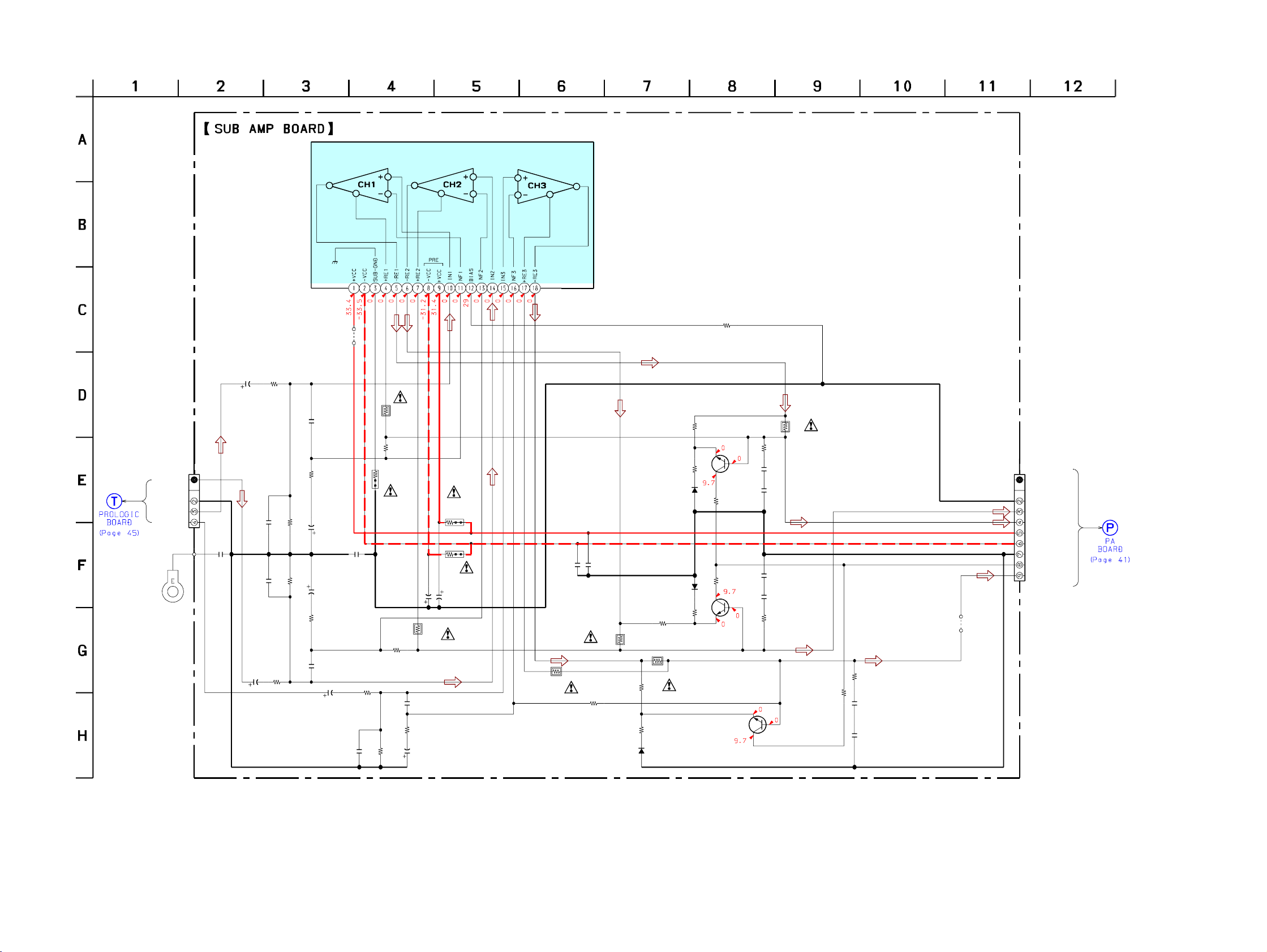
7-22.SCHEMATIC DIAGRAM – SUB AMP SECTION –
HCD-XGR90AV
IC101
STK443-050
AMP
R130
10k
101
JW
EPT101
CN102
CENTER
A.GND
REAR-L
REAR-R
(CHASSIS)
C101
R101
1k
1
50
C103
220p
4P
C102
R102
47k
680p
C114
1000p
C152
680p
C151
R152
47k
R151
1
50
1k
C154
R153
270
C153
220p
R103
330
C104
47
50
C113
10000p
47
50
C181
1
50
C182
680p
R181
R182
R128
0.22
2W
R110
47k
R120
1
0.22
Q101,151
OVER LOAD
2W
R191
1k
R192
15k
D191
1SS133T
R107
100
R168
0.22
2W
C105
R157
100
R138
0.22
C107
100
50V
2W
C157
100
50V
R160
47k
C183
R183
C184
220p
330
47
50
1k
47k
C106
0.1
0.1
TF
R190
47k
TF
R158
DETECT
R188
0.22
2W
R161
1k
D101
1SS133T
D151
1SS133T
R112
15k
R162
15k
R111
Q181
OVER LOAD
DETECT
1k
Q101
2SC1841
R113
100k
R163
100k
Q151
2SC1841
R109
10
1/2W
C108
0.068
C109
0.068
C159
0.068
C158
0.068
R159
10
1/2W
Q181
2SC1841
R108
0.22
2W
CN101
PE
PE
PE
PE
104
JW
R189
10
1/2W
R193
100k
C188
0.068
C189
0.068
9P
STK MUTE
SUB-GND
CENTER
REAR-L
+B
-B
GND
OVERLOAD
REAR-R
4343
Page 44

HCD-XGR90AV
7-23.PRINTED WIRING BOARD – PROLOGIC SECTION – • See page 21 for Circuit Boards Location.
1
PROLOGIC BOARD
A
B
C223
C226
C227
C231
C
D
E
C232
C235
C238
C229
C239
C228
C233
C253
212
JW
C224
C243
C221
C222
C234
C240
R211
C225
C244
R206
C241
211
JW
R209
C245
L201
R204
C242
R205
C251
C218
C219
C220
C237
1
2
C236
R207
40
41
C230
C247
R208
C248
C249
C250
R210
C246
CN202
R
C216
C217
C215
JW202
25 24
IC201
64 65
JW210
10
MAIN
BOARD
(Page 33)
C255
JW207
3 4 5 6
C264
R202
C212
C260
C259
201
JW
C211
R213
C206
C205
C202
C261
D201
C208
C203
R214
R217
C210
R271
R216
R282
R272
E
JW205
4
C207
Q271
219
JW
R292
Q281
T
R291
Q291
R293
R281
JW209
E
R283
R273
218
JW
CN203
1
SUB AMP
BOARD
E
JW204
CN201
10
C291
C292
R294
208
200
JW
JW
213
JW
206
JW
1
C214
C252
R203
FL201
C256
R201
C213
C262
C209
C204
1
80
C201
C258
R212
C257
JW214
JW215
JW216
JW217
(Page 42)
11
1-684-074-
(11)
S
MAIN
BOARD
(Page 33)
• Semiconductor
Location
Ref. No. Location
D201 A-4
IC201 B-3
Q271 B-4
Q281 B-4
Q291 A-5
4444
Page 45

7-24.SCHEMATIC DIAGRAM – PROLOGIC SECTION –
HCD-XGR90AV
CN202
10P
LT-IN
RT-IN
L-OUT
AGND
R-OUT
VRSWIN
C-IN
SL-IN
SR-IN
SW-IN
C253
220
16
100µH
C252
220
16
L201
C251
C249
47
16
R216
R217
R212
10k
10k
50
4.7
100k
10
C255
10
C256
10
C257
10
C258
10
C259
10
C260
10
C261
M62464FP
PRO-LOGIC SOUND
CONTROL
R213
100k
R206
150k
R209
150k
6800p
R211
100k
IC201
C250
50
50
50
50
50
50
50
R210
75k
C248
0.01
R214
100k
C247
0.01
C201
10
50
C202
10
50
R208
47k
C244
0.01
C245
0.01
R272
100k
2SC3623A
Q271
MUTE
R271
2.2k
R207
75k
R205
47k
50
0.47
C203
680p
C246
50
0.47
C204
C242
0.1
680p
C243
0.1
C205
R281
2.2k
R282
100k
Q281
2SC3623A
MUTE
C239
0.1
0.022
C241
0.1
C206
0.022
C240
50
0.47
C207
R292
100k
C238
0.1
50
0.47
C208
0.047
C237
R291
2.2k
50
0.47
C209
0.1
C235
0.047
C236
0.22
C234
50
0.47
C210
0.22
C233
50
0.47
C211
D201
50
4.7
C232
1SS355
50
4.7
C231
50
0.47
C212
0.22
0.22
C230
C229
0.1
C213
Q291
2SC3623A
MUTE
330k
R204
0.68
C228
0.047
C227
100
R201
78
5600p
C226
100
R202
79
C225
470
R203
77
1
50
C224
1000p
C223
4700p
C222
0.1
C221
0.22
C220
0.22
C219
C264
1000p
R293
10k
R283
10k
R273
10k
C291
0.01
C214
0.1
C218
C217
C216
FL201
0.1
1000p
4700p
1
50
R294
1k
C262
10
50
C292
0.01
C215
0.1
77
79
78
CN201
10P
SW-OUT
AGND
AGND
PL+10V
DGND
D+5V
PL-LAT
PL-CLK
PL-DAT
TA-MUT
CN203
4P
EH
REAR-R
REAR-L
AGND
CENTER
4545
Page 46
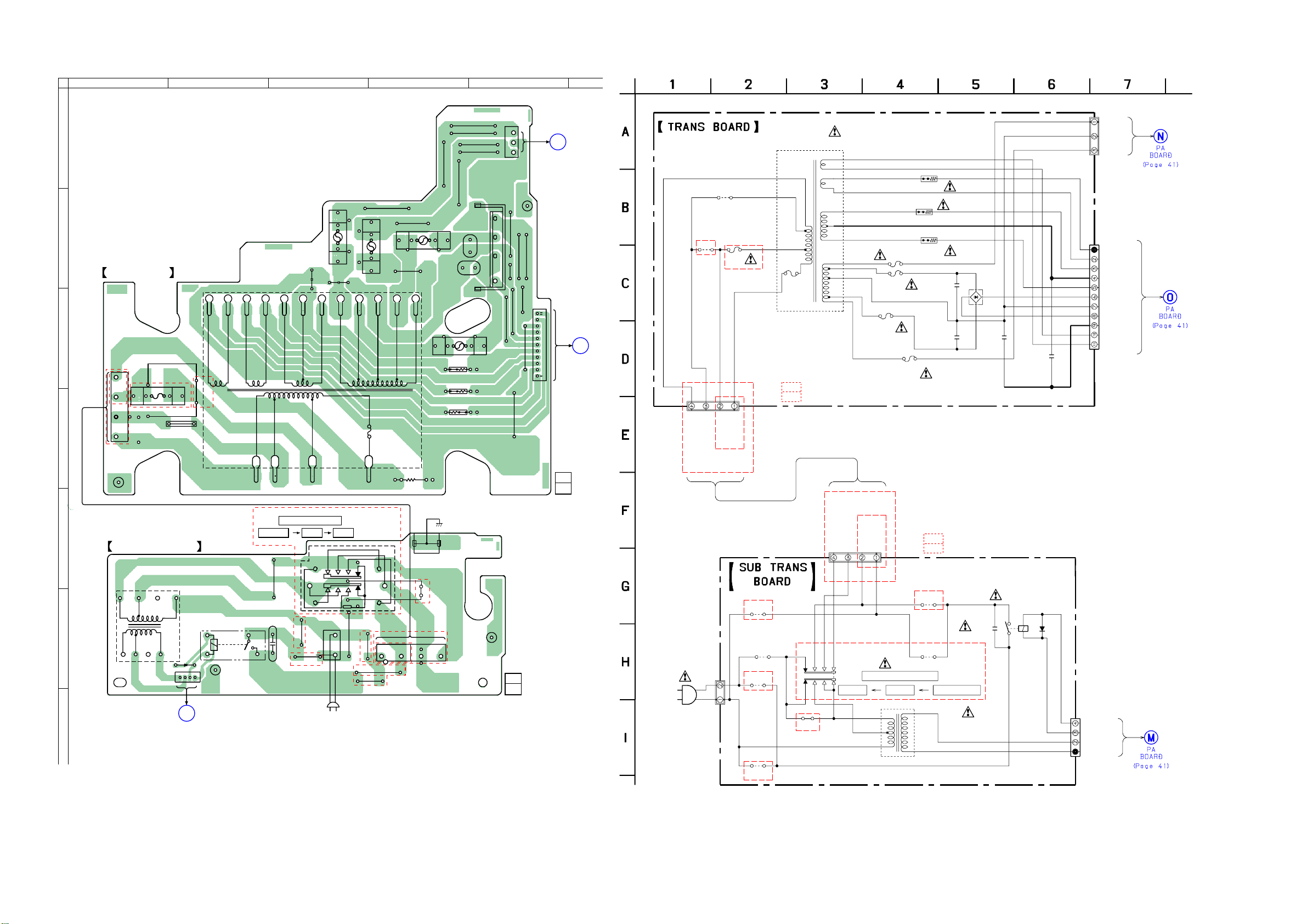
HCD-XGR90AV
C893
C834
CN901
R953
C963
C961
CN952
JW971
CN951
JW941
JW944
JW949
D832
RY901
D901
C901
NO903
S901
F962
F961
CN905
CN902
JW946
JW942
JW945
JW948
JW967
R951
R952
F951
F963
F964
0.1
100
0.1
100
2P
AMP
0.1
10000p
10000p
EH
VH-3P
D5SBA20
STANDBY
RELAY
9V
1SS133T
0.01
250V
T8.0AL
250V
T8.0AL
250V
33
33
T6.3AL
250V
T6.3AL
250V
T6.3AL
250V
VF
VF
AC IN
AC12V
AC12V
PRI-GND
AC7V
AC7V
AC-L
P-GND
AC-L
S-GND
STBY_RY
+9V
AC_IN
AC_IN
120V
230V
NEUTRAL
*
AC-H
AC-H
P-GND
230V
NEUTRAL
120V
230V
230V
240V
240V
POWER
TRANSFORMER
T951
BUILT IN TRANSFORMER
NOT REPLACEABLE:
*
TRANSFORMER
T901
SUB
VOLTAGE SELECTOR
120V
220-240V
220V
2P
4P
E
AUS
E
AUS
AUS
E
2P
4P
AUS
E
AUS
AUS
AUS
E
E
AUS
E
AUS
7-25.PRINTED WIRING BOARD – TRANS, SUB TRANS SECTION –
• See page 21 for Circuit Boards Location.
3 4 5
F961
C961
C963
S901
120V220V220-240V
E
901
N
C
941
JW
942
JW
S
AU
1
2
AC IN
1
2
A
B
TRANS BOARD
T951
POWER
TRANSFORMER
C
D
E
F
CN905
1
F951
2
S
AU
E
4
E
LP961
JW
SUB TRANS BOARD
T901
SUB
TRANSFORMER
NO903
1
E
950
JW
C901
VOLTAGE SELECTOR
967
JW
S
AU
971
RY901
D901
LP903
4
M
(Page 40)
PA
BOARD
G
F962
*
AU
44
9
JW
S
45
9
JW
JW946
JW949
E
7-26.SCHEMATIC DIAGRAM – TRANS, SUB TRANS SECTION –
0
96
JW
2
97
JW977
JW
JW
J
CN951
974
976
W
1
3
N
PA
BOARD
(Page 40)
JW978
980
JW
979
JW
F964
706
JW
* NOT REPLACEABLE:
BUILT IN TRANSFORMER
R961
F963
R952
R951
R
D832
C893
C834
953
(CHASSIS)
MT901
S
U
A
948
JW
E
US
A
2
1
S
AU
CN902
4
LP901
1-683-445-
LP963
–
JW702
JW982
--
JW981
+
JW984
JW983
JW985
JW986
JW975
JW973
1-683-444-
11
(11)
O
PA
BOARD
(Page 40)
CN952
11
(11)
4646
Page 47

r
p
p
WAVEFORMS
– MAIN BOARD – – BD BOARD –
IC101 el FE
IC501 qa XC-OUT
1
1
HCD-XGR90AV
32KHz
IC501 qd X-OUT
2
16MHz
T331 4
3
TAPE REC only
µ
sec
13
T331 5
4
TAPE REC only
3.0Vp-p
VOL/DIV : 1V AC
TIME/DIV : 10µsec
2.0Vp-p
VOL/DIV : 1V AC
TIME/DIV : 50nsec
240Vp-p
VOL/DIV : 50V AC
TIME/DIV : 10µsec
64Vp-p
IC101 ra TE
2
IC101 rd RFDC
3
IC101 yj XTAO
4
0.15Vp-p
VOL/DIV : 0.1V AC
TIME/DIV : 1msec
0.4Vp-
VOL/DIV : 0.2V AC
TIME/DIV : 0.2msec
0.62Vp-p
VOL/DIV : 0.2V AC
TIME/DIV : 0.5µsec
0.8Vp-p
µ
sec
13
VOL/DIV : 50V AC
TIME/DIV : 10µsec
– PANEL FL BOARD –
IC601 is X OUT
1
4MHz
VOL/DIV : 1V AC
TIME/DIV : 0.2µsec
16.9344MHz
VOL/DIV : 0.2V AC
TIME/DIV : 50nsec
2.4Vp-
47
Page 48

HCD-XGR90AV
7-27. IC PIN FUNCTIONS
• IC101 DIGITAL SIGNAL PROCESSOR (CXD3017Q) (BD Board)
Pin NamePin No.
1 SOSQ O Sub-Q serial output
2 SQCK I Clock input for SQSO read-out
3 XRST I System reset
4 SYSM I Muting input
5DATAISerial date input,supplied from CPU
6 XLAT I Latch input,supplied from CPU
7 CLOK I Serial date transfer clock input,supplied from CPU
8 SENS O SENS output
9 SCLK I SENS serial data read-out clock
10 VDD — Power supply (+3.3V)
11 ATSK — Input pin for anti-shock (Ground)
12 SPOA — Ground
13 SPOB — Ground
14 XLON O Not used (open)
15 WFCK O Not used (open)
16 XUGF O Not used (open)
17 XPCK O Not used (open)
18 GFS O Not used (open)
19 2SPO O Not used (open)
20 SCOR O Sub-code sync output
21 COUT I/O Not used (open)
22 MIRR I/O Not used (open)
23 DFCT I/O Not used (open)
24 FOK I/O Not used (open)
25 LOCK I/O Not used (open)
26 MDP O Output to control spindle motor servo
27 SSTP I Input signal to detect disc inner most trak
28 SFDR O Sled drive output
29 SRDR O Sled drive output
30 TFDR O Tracking drive output
31 TRDR O Tracking drive output
32 FFDR O Focus drive output
33 FRDR O Focus drive output
34 VSS — Ground
35 TEST I TEST pin (connected to ground)
36 TES1 I TEST pin (connected to ground)
37 XTSL I X’tal selection circuit input (connected to ground)
38 VC I Center voltage input
39 FE I FOCUS error signal input
40 SE I Sled error signal input
41 TE I Tracking error signal input
42 CE I Center servo analog input
43 RFDC I RF signal input
44 ADIO O Not used (open)
45 AVSS0 — Analog ground
46 IGEN I Power supply pin operational amplifiers
47 AVDDO — Power supply (+3.3V)
48 ASYO O EFM full swing output
49 ASYI I Asymmetry comparator voltage input
50 BIAS I Asymmetry circuit constant current input
51 RFAC I EFM signal input
52 AVSS3 — Ground
I/O
Description
48
Page 49

HCD-XGR90AV
Pin No.
53 CLTV I Control voltage input for master VCO
54 FILO O Filter output for master PLL
55 FILI I Filter input for master PLL
56 PCO O Chage-pump output for master PLL
57 AVDD3 — Powr supply (+3.3V)
58 VSS — Ground
59 VDD — Power supply (+3.3V)
60 DOUT O CD data output
61 LRCK O Not used (open)
62 PCMD O Not used (open)
63 BCK O Not used (open)
64 EMPH O Not used (open)
65 XVDD — Power supply (+3.3V)
66 XTAI I X’tal oscillator circuit input (16.9344MHz)
67 XTAO O X’tal oscillator circuit output (16.9344MHz)
68 XVSS — Ground
69 AVDD1 — Power supply (+3.3V)
70 AOUT1 O Lch : Analog output
71 AIN1 I Lch : OPAMP input
72 LOUT1 O Lch : LINE output
73 AVSS1 — Ground
74 AVSS2 — Ground
75 LOUT2 O Rch : LINE output
76 AIN2 I Rch : OPAMP input
77 AOUT2 O Rch : Analog output
78 AVDD2 — Power supply (+3.3V)
79 RMUT O Not used (open)
80 LMUT O Not used (open)
I/O
DescriptionPin Name
49
Page 50

HCD-XGR90AV
• IC501 M30620MCN-A01FP SYSTEM CONTOL (MAIN Board)
Pin No.
1 AUDIO-OUT O MD output mute signal output
2 STEREO I Stereo signal input
3 TUNED I Tuned signal input
4 SIRCS I SIRCS input
5 CD-MUTE O CD mute signal output
6– —Not used (open)
7– —Not used (open)
8 BYTE I Not used (connected to ground)
9 CNVSS — Not used (Connected to ground with resistor)
10 XC-IN I Sub clock input
11 XC-OUT O Sub clock output
12 RESET I System reset input
13 X-OUT O Main system clock output (16MHz)
14 VSS — Ground
15 X-IN I Main system clock input (16MHz)
16 VCC — Power supply (+5V)
17 NMI I Not used (Pull up with resistor)
18 RDS-INT I Not used (Connected to ground with resistor)
19 SCOR I CD Q-Data request input
20 AC-CUT I AC cut check signal input
21 ST-MUTE O Tuner mute signal output
22 ST-CE O Tuner chip enable signal output
23 ST-DOUT O Tuner data output
24 BU-PWM3 O BU PWM 3 (for CD-RW) signal output
25 ST-DIN I Tuner data input
26 BU-PWM2 O BU PWM 2 (for CD-RW) signal output
27 ST-CLK O Tuner clock signal output
28 BU-PWM1 O BU PWM 1 (for CD-RW) signal output
29 IIC-CLK I IIC serial data clock input
30 IIC-DATA I IIC serial data input
31 – — Not used (open)
32 SQ-DATA I CD data input
33 SQ-CLK O CD data clock output
34 SENS I SENS signal input from CXD3017Q
35 CD-DATA O CD data output to CXD3017Q
36 XLT O CD latch signal output to CXD3017Q
37 CD-CLK O CD data clock output to CXD3017Q
38 CD-POWER O CD power on/off signal output
39 CLK-OUT O Not used (open)
40 HOLD O Laser diode control signal output
41 OTM-RESET O Other micom reset
42 – — Not used (open)
43 XRST O CD reset signal output
44 MTR-CTRL1 O CD motor control 1 output
45 MTR-CTRL2 O CD motor control 2 output
46 REC-A I Record tab switch for SIDE-A signal input
47 LED-DISC O DISC LED on/off signal output
48 BU UP/DW SW I BU up switch signal input
49 TBL-SENS I Table sensor signal input
50 REC-B I Record tab switch for SIDE-B signal input
51 A-TRG O TCM-A trigger output
52 B-TRG O TCM-B Trigger output
53 AMS-IN I AMS signal input
Pin Name
I/O
Description
50
Page 51

HCD-XGR90AV
Pin No.
54 CAPM-H/L O Capstan motor high/low signal output
55 CAPM-CTRL O Capstan motor REV/FWD/STOP control signal output
56 A-PLAY I TCM-A play switch input
57 B-PLAY I TCM-B play switch input
58 TC-MUTE O TC line mute signal output
59 REC/PB/PASS O Video input select signal output (A)
60 NR ON/OFF O Video input select signal output (B)
61 REC-MUTE O REC mute signal output
62 VCC — Power supply (+3.3V)
63 SOFT-TEST O Soft check output
64 VSS — Ground
65 BIAS O Bias on/off signal output
66 EQ-H/N O EQ high/Normal signal output
67 PB-A/B O TC A/B select signal output
68 ALC O ALC signal output
69 TC-RELAY O TC relay control signal output
70 A-HALF I A deck half detection signal input
71 FUNC-SEL0 O Function select A signal output
72 FUNC-SEL1 O Function select B signal output
73 KEY-ECO I ECO key signal input
74 KEY-POWER I Power key signal input
75 LED-STBY O Standby LED driver signal output
76 VIDEO-MUTE O Video mute signal output
77 PL-LAT O Prologic sound control LAT signal
78 PL-DAT O Prologic sound control data
79 PL-CLK O Prologic sound control clock
80 EQIC-DAT O Serial data output to Audio EQIC
81 EQIC-CLK O Serial data clock output to Audio EQIC
82 LINE-MUTE O TA LINE mute signal output
83 STK-MUTE O Mute signal output to power IC
84 STBY-RELAY O Standby relay driver signal output
85 REAR-RELAY O Rear speaker relay driver signal output
86 HP-MUTE O Headphone mute signal output
87 FRONT-RELAY O Front speaker relay driver signal output and woofer mute signal
88 PROTECT I Speaker protection signal input
89 A-SHUT I TCM-A reel pulse input
90 B-SHUT I TCM-B reel pulse input
91 B-HALF I B deck half detection input
92 MODEL-IN I Model input
93 DEST-IN I Destination input
94 DBFB-H/L O DBFB high/low signal output
95 HP-IN I Headphone detect input
96 AVSS — Ground
97 SW-MODE O Super woofer mode signal output
98 VREF I Reference voltage input
99 AVCC — Power supply (+3.3V)
100 RDS-DATA I Not used (Connected to ground)
Pin Name
I/O
Discription
51
Page 52

HCD-XGR90AV
• IC601 MB90M407APF-G-112-BND DISPLAY CONTROL (PANEL FL Board)
Pin No.
1 to 10 GR-16 to GR-7 O FLD grid output
11 VSS-IO — Ground
12 to 17 GR-6 to GR-1 O FLD grid output
18 to 22 SEG-1 to SEG-5 O FLD segment output
23 VDD-FIP — Power supply (+3.3V)
24 to 41 SEG-6 to SEG-23 O FLD segment output
42 VSS-IO — Ground
43,44 SEG-24, SEG-25 O FLD segment output
45 to 47 NO USED O Not used (open)
48 VKK — Power supply (-35V)
49 MD0 I Not used (pull up with resistor)
50 MD1/VDD-VFT I Not used (pull up with resistor)
51 MD2 I Not used (pull down with resistor)
52 D-SW I CD lid open/close detect signal input
53 DIST O Guitar distortion ON/OFF signal output
54 SOFT TEST O Not used (open)
55 LED SELB O LED group B select signal output
56 VOL A I Volume encoder signal A input
57 VOL B I Volume encoder signal B input
58 JOG A I AMS jog dial encoder signal A input
59 JOG B I AMS jog dial encoder signal B input
60 I2C-DATA O IIC serial data output
61 I2C-CLOCK O IIC clock signal output
62 AVCC — Power supply (+3.3V)
63 AVSS — Ground
64 to 69 KEY0 to KEY5 I Key input (A/D port)
70 to 74 BPF1-F02 to BPF1-F06 I Spectrum analyzer BPF signal input
75 ALL BAND I L+R signal input
76 LED-SCK O Serial clock output to LED driver
77 RESET I Reset input
78 LED-DAT O Serial data output to LED driver
79 LED-LATCH O Latch signal output to LED driver
80 LED-SELA O LED group A select signal output
81 VSS-CPU — Ground
82 XOUT O Crystal oscillator output (4MHz)
83 XIN I Crystal oscillator input (4MHz)
84 VCC-CPU — Power supply (+3.3V)
85 to 100 NO USED O Not used (open)
Pin Name
I/O
Description
52
Page 53

7-28. IC BLOCK DIAGRAMS
IC101 CXD3017Q (BD BOARD)
HCD-XGR90AV
LRCK
PCMD
BCK
EMPH
XVDD
XTAI
XTAO
XVSS
AVDD1
AOUT1
AIN1
LOUT1
AVSS1
AVSS2
LOUT2
AIN2
AOUT2
AVDD2
RMUT
LMUT
8
CLTV
SENS
AVSS
52
Servo Auto
Sequencer
SERVO
Interface
9
SCLK
RFAC
51
Demodurator
11
10
VDD
BIAS
50 49
Asymmetry
Corrector
EFM
12 13
ATSK
SPOA
14
SPOB
ASYI
15 16 17
XLON
WFCK
AVDD
ASYO
47 46 45
48
SERVO DSP
TRACKING
18 19 20
GFS
XUGF
XPCK
FOCUS
SERVO
SERVO
SELED
SERVO
C2PO
IGEN
Converter
AVSS
4453
A/D
ADIO
SCOR
RFDC
OP Amp
Analog SW
Clock
Generator
PWM
GENERATOR
FOCUS PWM
GENERATOR
TRACKING
PWM
GENERATOR
SLED PWM
GENERATOR
Digital
CLV
MIRR
DFCT
FOK
CE
TE
414243
SE
40
39
FE
VC
38
XTSL
37
TES1
36
TEST
35
VSS
34
FRDR
33
FFDR
32
31
TRDR
30
TFDR
29
SRDR
28
SFDR
27
SSTP
26
MDP
LOCK
25
FOK
24
DFCT
23
22
MIRR
COUT
21
VSS
VDD
DOUT
60
Digital
OUT
61
62
63
64
65
66
67
68
69
70
71
72
73
74
75
76
77
78
79
80
Timing
Logic
PWM
D/A
Interface
3rd-Order
Noise Shaper
58
59
Serial-In
Interface
Over Sampling
Digital Filter
PWM
1 2
SQSO
57
SQCK
AVDD
3
XRST
4
SYSM
PCO
56
5
Corrector
Sub Code
Processor
DATA
55
Error
16K
RAM
FILI
Digital
PLL
CPU
Interface
6
XLAT
FILO
54
7
CLOK
IC102 BA5974FM-E2 (BD BOARD)
PRFVCC
1 2 3 4 5 6 7 8 9 10 11 12 13 14
VREFOUT
CH4BIN
INTERFACE
CH1FIN
CH4SIN'
RF
CH1RIN
CH4SIN
F
R
CAPAIN1
CH3FIN
F
INTERFACE
INTERFACE
CH2FIN
CH3RIN
R
RF
CH2RIN
MUTE
POWVCC
CH3OUTR
CH3OUTF
CH4OUTR
CH1OUTR
CH4OUTF
CH1OUTF
CAPAIN3
R
F
F
R
CAPAIN2
MUTE
GND
202122232425262728 19 18 17 16 15
THERMAL
SHUTDOWN
GND
VREFIN
POWVCC
CH2OUTR
CH2OUTF
LEVEL SHIFT
53
Page 54

HCD-XGR90AV
IC103 CXA2581N-T4 (BD BOARD)
AC
SUM
APC
EQ IN
AC SUM
GND
1LD
2
PD
3
4
5
6
A
7
B
8
C
9
D
RW/ROM
VOFST
RW/ROM
30
DC_OFST
RW/ROM
RFDCI
DVCC
VC
VOFST
B
C
A
D
VC
RW/ROM
VC
VCC
EQ
ON/OFF
VC
DVC
VCC
EQ
AC
VCA
VCC
29
RFDCO
28
VC
27
VC
26
RFC
25
VFC
24
BST
23
RFG
VCC
22
21
CEI
CE
20
TE_BAL
19
gm
gm
APC-OFF(Hi-Z)
RW/ROM
(H/L)
DVC
SW
DVCC
DVC
RFAC
10
F
11
E
12
13
14
15
IC321 µPC1330HA (MAIN BOARD (3/3))
2
3
1
SW R1 GND SW P1
4
CONT GND VCC SW P2 GND
AVC
DVC
VC
INVERTER
COMPARATER
5 6 7 8 9
DVC
VOFST
SW R2
RW/ROM
DVC
DVCC
DVCC
RW/ROM
TE
18
FEI
17
FE
16
54
Page 55

IC191 BA7615N (MAIN BOARD (1/3))
HCD-XGR90AV
MUTE
1
2
4
3
CTLA
CTLB
IN2
IN1
6db
LOGIC
6
7
5
IN3
VCC
CTLC
IC201 TA8409S (MOTOR BOARD)
STANDBY
BLOCK
75Ω
10
8
9
IN4
GND
VOUT
VREF
BLOCK
HEAT
CUT OFF
BLOCK
2 3
1
VCC OUT2 NC GND
IN2
IC602 BA3830F (PANEL FL BOARD)
REFERENCE
1
R02
R01
LINE NF
LINE IN
REC NF
REC IN
RESET C
BIAS C
GND
2
3
4
5
6
7
8
9
CURRENT
REFERENCE
CURRENT
–
+
–
+
4
FILTER
BAND
PASS
5 6
RESET
DET
7
VS
OUT1 VREF IN1
18
17
16
15
14
13
12
11
10
8
RESET
F01
F02
F03
F04
F05
F06
REC LEVEL
VCC
9
55
Page 56

HCD-XGR90AV
NOTE:
• -XX, -X mean standardized parts, so they may
have some differences from the original one.
• Items marked “*” are not stocked since they
are seldom required for routine service. Some
delay should be anticipated when ordering these
items.
• The mechanical parts with no reference number
in the exploded views are not supplied.
8-1. CASE, BACK PANEL SECTION
SECTION 8
EXPLODED VIEWS
• Hardware (# mark) list and accessories are
given in the last of this parts list.
• Abbreviation
AUS : Australian model
The components identified by
mark 0 or dotted line with mark
0 are critical for safety.
Replace only with part number
specified.
3
#3
4
#1
5
2
a
not
supplied
#1
#1
not supplied
#1
6
#1
#2
#1
#1
#1
#1
#1
2
M901
Front panel section
1
#1
Ref. No. Part No. Description Remarks
1 4-948-236-21 CUSHION (107)
2 3-363-099-01 SCREW (CASE 3 TP2)
3 4-237-661-11 CASE
4 1-693-572-11 TUNER (FM/AM) (AUS)
4 1-693-574-11 TUNER (FM/AM) (E)
5 1-769-945-11 WIRE (FLAT TYPE) (11 CORE)
56
Chassis section
a
#1
Ref. No. Part No. Description Remarks
6 4-238-825-01 PANEL, BACK (E)
6 4-238-825-11 PANEL, BACK (AUS)
M901 1-763-072-11 FAN, DC
#1 7-685-646-79 SCREW +BVTP 3X8 TYPE2 N-S
#2 7-685-872-09 SCREW +BVTT 3X8 (S)
#3 7-685-871-01 SCREW +BVTT 3X6 (S)
Page 57

8-2. FRONT PANEL SECTION-1
55
56
57
HCD-XGR90AV
59
54
not supplied
58
not supplied
51
54
52
53
54
62
63
65
54
54
60
54
54
63
54
not supplied
64
61
54
#1
Ref. No. Part No. Description Remarks
51 4-237-635-01 KNOB (MIC)
52 A-4727-633-A MIC/GUITAR BOARD, COMPLETE
53 1-683-448-11 TC-A BOARD
54 4-951-620-01 SCREW (2.6X8), +BVTP
55 4-237-648-01 COVER (EJECT)
56 4-237-645-01 LEVER (EJECT-A)
57 4-237-647-01 LEVER (EJECT-C)
58 4-237-646-01 LEVER (EJECT-B)
Front panel section-2
Ref. No. Part No. Description Remarks
59 4-237-659-01 SPRING (LEVER)
60 1-796-333-11 DECK, MECHANICAL
61 1-773-021-11 WIRE (FLAT TYPE) (15 CORE)
62 1-683-449-11 TC-B BOARD
63 3-354-963-01 DAMPER
64 1-683-450-11 HEADPHONE BOARD
65 1-684-683-11 D-SW BOARD
#1 7-685-646-79 SCREW +BVTP 3X8 TYPE2 N-S
57
Page 58

HCD-XGR90AV
8-3. FRONT PANEL SECTION-2
not supplied
109
114
112
109
106
104
105
103
102
#6
109
108
#6
107
119
109
109
118
supplied with S763
not supplied
FL601
110
109
117
109
110
123
111
109
not
supplied
109
113
109
114
115
109
109
116
101
120
109
121
122
109
Ref. No. Part No. Description Remarks Ref. No. Part No. Description Remarks
101 4-237-649-31 BUMPER (PANEL)
102 1-683-452-11 CD-L BOARD
103 X-4954-371-1 SUB PANEL (CD-L) ASSY
104 4-237-638-01 LID(CD)
105 4-237-630-01 WINDOW (CD)
106 4-237-658-01 SPRING (CD)
107 4-040-472-01 LATCH, D.C.
108 4-237-634-01 KNOB (VOLUME)
109 4-951-620-01 SCREW (2.6X8), +BVTP
* 110 4-949-935-81 CUSHION (FL)
111 4-225-511-01 HOLDER FL TUBE
112 A-4727-623-A PANEL FL BOARD, COMPLETE
113 1-773-118-11 WIRE (FLAT TYPE) (19 CORE)
114 4-237-639-01 HOLDER (LED 1)
115 1-773-178-11 WIRE (FLAT TYPE) (23 CORE)
116 A-4727-609-A PANEL VR BOARD, COMPLETE
117 X-4954-379-1 FRONT PANEL ASSY
118 4-224-104-01 DAMPER
119 X-4954-372-1 SUB PANEL (CD-R) ASSY
120 4-237-636-01 KNOB (CD)
121 1-683-453-11 CD-R BOARD
122 1-683-454-11 FRONT INPUT BOARD
123 4-237-640-01 HOLDER (LED 2)
FL601 1-518-794-11 INDICATOR TUBE, FLUORESCENT
#6 7-685-533-19 SCREW +BTP 2.6X6 TYPE2 N-S
58
Page 59

8-4. CHASSIS SECTION
#1
157
#1
not supplied
#4
153
not supplied
#1
#4
#1
not supplied
#2
T951
b
F963
#5
154
F964
F962
#1
#5
F961
F951
b
155
159
156
not supplied
HCD-XGR90AV
158
#2
162
160
152
CDM37B-30BD60C
151
not supplied
#1
not supplied
not supplied
#1
#1
#1
161
#1
The components identified by
mark 0 or dotted line with mark
0 are critical for safety.
Replace only with part number
specified.
Ref. No. Part No. Description Remarks Ref. No. Part No. Description Remarks
151 1-823-750-11 WIRE (FLAT TYPE) (21 CORE)
152 4-235-701-01 DUST COVER
153 A-4727-607-A PA BOARD COMPLETE (AUS)
153 A-4728-672-A PA BOARD COMPLETE (E)
154 1-683-444-11 TRANS BOARD
155 3-703-244-00 BUSHING (FBS001), CORD (AUS)
155 4-966-266-01 BUSHING (S) (FBS002), CORD (E)
0 156 1-696-847-11 CORD, POWER (AUS)
0 156 1-791-901-11 CORD, POWER (E)
157 A-4727-612-A SUB AMP BOARD, COMPLETE
158 1-683-445-11 SUB TRANS BOARD
161 X-4941-228-1 FOOT (F22125H-M)
162 A-4727-611-A PROLOGIC BOARD, COMPLETE
0 F951 1-532-506-31 FUSE (T6.3AL 250V)(E)
0 F961 1-533-949-31 FUSE, CYLINDRICAL (TIME LUG) (T8.0AL 250V)
0 F962 1-533-949-31 FUSE, CYLINDRICAL (TIME LUG) (T8.0AL 250V)
0 F963 1-532-506-31 FUSE (T6.3AL 250V)
0 F964 1-532-506-31 FUSE (T6.3AL 250V)
0 T951 1-435-249-11 TRANSFORMER, POWER
#1 7-685-646-79 SCREW +BVTP 3X8 TYPE2 N-S
#2 7-685-872-09 SCREW +BVTT 3X8 (S)
#4 7-685-650-79 SCREW +BVTP 3X16 TYPE2 IT-3
* 159 4-988-533-01 HOLDER, PWB
160 A-4440-760-A MAIN BOARD, COMPLETE (AUS)
160 A-4676-333-A MAIN BOARD, COMPLETE (E)
#5 7-685-881-09 SCREW +BVTT 4X8 (S)
59
Page 60

HCD-XGR90AV
8-5. CD MECHANISM DECK SECTION
(CDM37B-30BD60C)
501
509
504
510
501
505
#1
507
511
506
501
503
502
513
502
#1
#1
512
M201
510
514
#1
516
515
BU-30BD60C
#1
520
518
519
520
522
521
517
508
510
520
518
519
520
521
524
523
Ref. No. Part No. Description Remarks Ref. No. Part No. Description Remarks
501 4-987-976-01 SCREW, STEP
502 4-944-490-01 BELT (TIMING)
503 A-4660-978-A GEAR (PULLEY) ASSY
504 4-978-421-01 GEAR (MID)
505 4-978-425-01 ROLLER (CAM)
506 4-978-420-01 CAM (HOLDER)
507 4-237-981-01 PULLEY (B) (30), CHUCKING
508 X-4953-307-1 PULLEY (A) ASSY, CHUCKING
509 4-238-261-01 TABLE, DISK
510 X-4947-960-1 ROLLER ASSY
* 511 4-978-583-01 BRACKET (BU)
512 4-238-260-01 CHASSIS
* 513 A-4673-765-A MOTOR BOARD, COMPLETE
514 4-978-426-01 INDICATOR (NO.)
* 515 1-659-059-13 LED BOARD
* 516 1-659-058-13 SENSOR BOARD
517 4-228-414-01 BRACKET (YOKE)
518 4-951-620-01 SCREW (2.6X8), +BVTP
519 4-231-151-01 STOPPER (BU)
520 4-231-451-11 INSULATOR (BU-30)
521 4-227-045-11 SPRING (INSULATOR), COIL
522 4-227-899-01 SCREW (DIA. 12), FROATING
523 4-998-716-01 SCREW, BU FITTING
524 X-4954-451-1 HOLDER (BU30) ASSY
M201 A-4660-977-A MOTOR ASSY
#1 7-685-646-79 SCREW +BVTP 3X8 TYPE2 N-S
60
Page 61
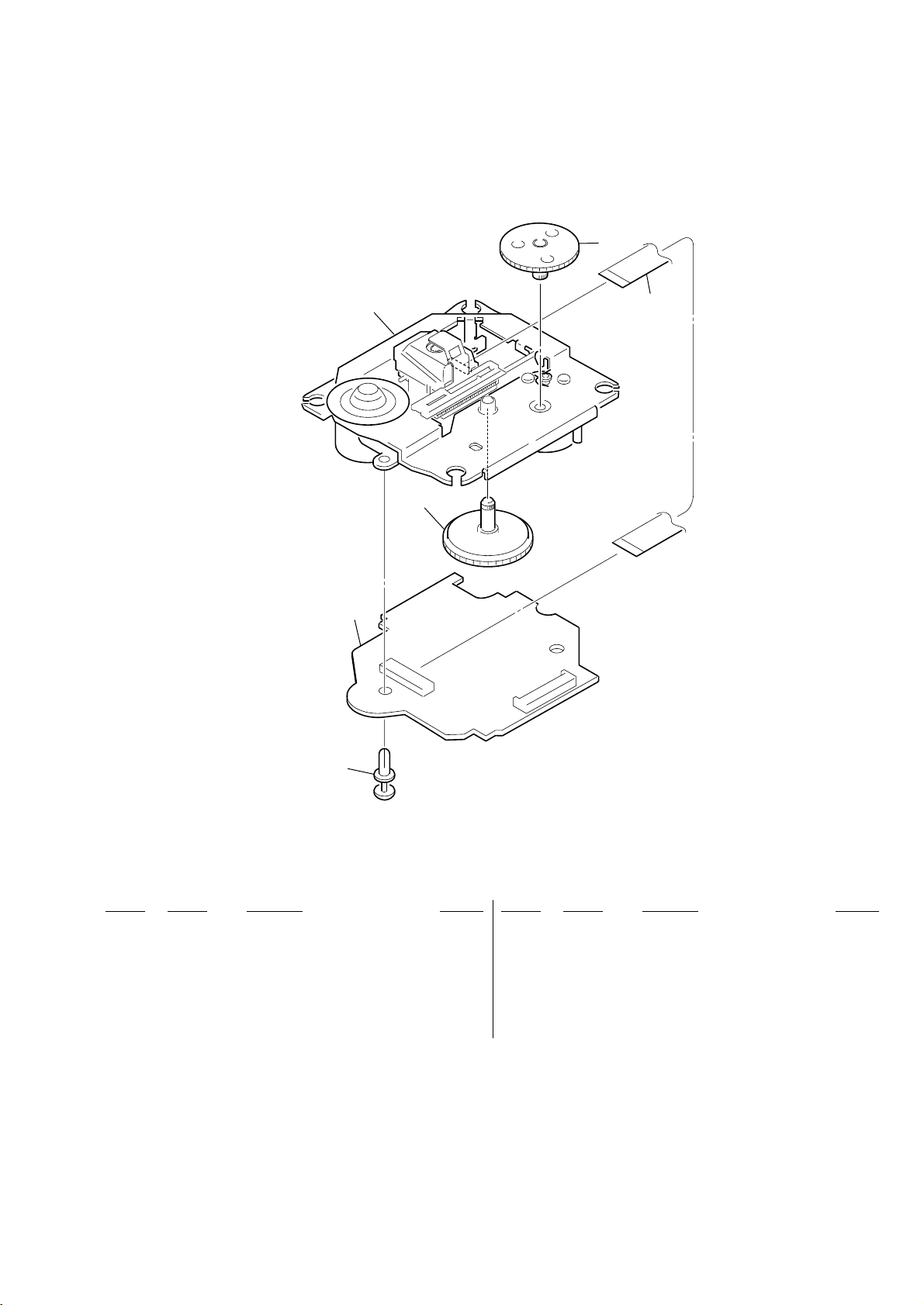
8-6. BASE UNIT SECTION
(BU-30BD60C)
HCD-XGR90AV
554
552
556
555
553
551
Ref. No. Part No. Description Remarks Ref. No. Part No. Description Remarks
551 3-531-576-11 RIVET
552 A-4728-678-A BD BOARD, COMPLETE
553 4-233-832-01 GEAR (LB)
554 4-233-831-01 GEAR (LA)
555 1-757-710-11 WIRE (FLAT TYPE) (16 CORE)
556 A-4735-188-A BU-30 (60) ASSY
61
Page 62

HCD-XGR90AV
SECTION 9
BD
NOTE:
Ref. No. Part No. Description Remarks Ref. No. Part No. Description Remarks
• Due to standardization, replacements in the
parts list may be different from the parts
specified in the diagrams or the components
used on the set.
• -XX, -X mean standardized parts, so they
may have some difference from the original
one.
• Items marked “*” are not stocked since they
are seldom required for routine service.
Some delay should be anticipated when
ordering these items.
• RESISTORS
All resistors are in ohms.
METAL: metal-film resistor
MET AL OXIDE: Metal Oxide-film resistor
F: nonflammable
Ref. No. Part No. Description Remarks Ref. No. Part No. Description Remarks
A-4728-678-A BD BOARD, COMPLETE
C101 1-162-967-11 CERAMIC CHIP 0.0033uF 10% 50V
C102 1-107-826-11 CERAMIC CHIP 0.1uF 10% 16V
C103 1-162-962-11 CERAMIC CHIP 470PF 10% 50V
C104 1-162-962-11 CERAMIC CHIP 470PF 10% 50V
C108 1-107-826-11 CERAMIC CHIP 0.1uF 10% 16V
C109 1-162-965-11 CERAMIC CHIP 0.0015uF 10% 50V
C110 1-162-967-11 CERAMIC CHIP 0.0033uF 10% 50V
C111 1-162-927-11 CERAMIC CHIP 100PF 5% 50V
C112 1-125-837-91 CERAMIC CHIP 1uF 10% 6.3V
C114 1-164-360-11 CERAMIC CHIP 0.1uF 16V
*****************
< CAPACITOR >
ELECTRICAL PARTS LIST
• CAPACITORS:
uF: µF
• COILS
uH: µH
• SEMICONDUCTORS
In each case, u: µ, for example:
uA...: µA... , uPA... , µPA... ,
uPB... , µPB... , uPC... , µPC... ,
uPD..., µPD...
• Abbreviation
AUS : Australian model
C193 1-104-665-11 ELECT 100uF 20% 10V
C194 1-164-360-11 CERAMIC CHIP 0.1uF 16V
C195 1-164-360-11 CERAMIC CHIP 0.1uF 16V
C196 1-164-360-11 CERAMIC CHIP 0.1uF 16V
C197 1-107-826-11 CERAMIC CHIP 0.1uF 10% 16V
C198 1-124-584-00 ELECT 100uF 20% 10V
CN101 1-568-864-11 CONNECTOR, FFC 21P
CN102 1-793-907-11 CONNECTOR, FFC/FPC 16P
D101 8-719-083-58 DIODE UDZSTE-173.9B
The components identified by
mark 0 or dotted line with mark
0 are critical for safety.
Replace only with part number
specified.
When indicating parts by reference
number, please include the board
name.
< CONNECTOR >
< DIODE >
C116 1-104-665-11 ELECT 100uF 20% 10V
C117 1-104-665-11 ELECT 100uF 20% 10V
C118 1-162-964-11 CERAMIC CHIP 0.001uF 10% 50V
C121 1-164-360-11 CERAMIC CHIP 0.1uF 16V
C122 1-124-584-00 ELECT 100uF 20% 10V
C123 1-162-970-11 CERAMIC CHIP 0.01uF 10% 25V
C124 1-125-891-11 CERAMIC CHIP 0.47uF 10% 10V
C125 1-164-360-11 CERAMIC CHIP 0.1uF 16V
C126 1-164-360-11 CERAMIC CHIP 0.1uF 16V
C127 1-124-584-00 ELECT 100uF 20% 10V
C129 1-162-974-11 CERAMIC CHIP 0.01uF 50V
C130 1-164-360-11 CERAMIC CHIP 0.1uF 16V
C131 1-104-665-11 ELECT 100uF 20% 10V
C133 1-162-921-11 CERAMIC CHIP 33PF 5% 50V
C143 1-164-360-11 CERAMIC CHIP 0.1uF 16V
C145 1-164-360-11 CERAMIC CHIP 0.1uF 16V
C153 1-164-360-11 CERAMIC CHIP 0.1uF 16V
C159 1-162-970-11 CERAMIC CHIP 0.01uF 10% 25V
C162 1-104-665-11 ELECT 100uF 20% 10V
C165 1-164-360-11 CERAMIC CHIP 0.1uF 16V
C167 1-162-919-11 CERAMIC CHIP 22PF 5% 50V
C168 1-162-921-11 CERAMIC CHIP 33PF 5% 50V
C171 1-115-412-11 CERAMIC CHIP 680PF 5% 25V
C172 1-162-927-11 CERAMIC CHIP 100PF 5% 50V
C181 1-115-412-11 CERAMIC CHIP 680PF 5% 25V
C182 1-162-927-11 CERAMIC CHIP 100PF 5% 50V
C183 1-164-227-11 CERAMIC CHIP 0.022uF 10% 25V
C184 1-162-970-11 CERAMIC CHIP 0.01uF 10% 25V
C185 1-125-837-91 CERAMIC CHIP 1uF 10% 6.3V
C190 1-115-156-11 CERAMIC CHIP 1uF 10V
< FERRITE BEAD >
FB101 1-500-445-21 FERRITE 0UH
FB102 1-500-445-21 FERRITE 0UH
< IC >
IC101 8-752-402-31 IC CXD3017Q
IC102 8-759-827-41 IC BA5974FM-E2
IC103 8-752-089-74 IC CXA2581N-T4
< JUMPER RESISTOR >
JR101 1-216-864-11 METAL CHIP 0 5% 1/16W
JR102 1-216-864-11 METAL CHIP 0 5% 1/16W
JR103 1-216-864-11 METAL CHIP 0 5% 1/16W
JR104 1-216-864-11 METAL CHIP 0 5% 1/16W
JR105 1-216-864-11 METAL CHIP 0 5% 1/16W
JR106 1-216-864-11 METAL CHIP 0 5% 1/16W
JR122 1-216-296-11 SHORT 0
JR123 1-216-296-11 SHORT 0
JR124 1-216-296-11 SHORT 0
JR125 1-216-296-11 SHORT 0
< COIL >
L101 1-469-553-21 INDUCTOR 4.7uH
< TRANSISTOR >
Q101 8-729-049-31 TRANSISTOR 2SB710A-RTX
Q102 8-729-920-85 TRANSISTOR 2SD1664-T100-QR
< RESISTOR >
C191 1-124-584-00 ELECT 100uF 20% 10V
C192 1-164-360-11 CERAMIC CHIP 0.1uF 16V
62
R101 1-216-821-11 METAL CHIP 1K 5% 1/16W
R102 1-216-845-11 METAL CHIP 100K 5% 1/16W
Page 63

HCD-XGR90AV
BD CD-L CD-R D-SW FRONT INPUT
Ref. No. Part No. Description Remarks Ref. No. Part No. Description Remarks
R103 1-216-835-11 METAL CHIP 15K 5% 1/16W
R104 1-216-839-11 METAL CHIP 33K 5% 1/16W
R105 1-216-821-11 METAL CHIP 1K 5% 1/16W
R773 1-249-421-11 CARBON 2.2K 5% 1/4W F
R774 1-247-843-11 CARBON 3.3K 5% 1/4W
R775 1-249-425-11 CARBON 4.7K 5% 1/4W F
R106 1-216-821-11 METAL CHIP 1K 5% 1/16W
R107 1-216-833-11 METAL CHIP 10K 5% 1/16W
R108 1-216-827-11 METAL CHIP 3.3K 5% 1/16W
R109 1-216-857-11 METAL CHIP 1M 5% 1/16W
R111 1-216-846-11 METAL CHIP 120K 5% 1/16W
R114 1-218-745-11 RES-CHIP 160K 5% 1/10W
R116 1-216-001-00 METAL CHIP 10 5% 1/10W
R117 1-216-821-11 METAL CHIP 1K 5% 1/16W
R118 1-216-809-11 METAL CHIP 100 5% 1/16W
R119 1-216-826-11 METAL CHIP 2.7K 5% 1/16W
R120 1-216-835-11 METAL CHIP 15K 5% 1/16W
R122 1-216-845-11 METAL CHIP 100K 5% 1/16W
R123 1-216-833-11 METAL CHIP 10K 5% 1/16W
R124 1-216-845-11 METAL CHIP 100K 5% 1/16W
R131 1-216-813-11 METAL CHIP 220 5% 1/16W
R143 1-216-839-11 METAL CHIP 33K 5% 1/16W
R144 1-216-839-11 METAL CHIP 33K 5% 1/16W
R147 1-218-701-11 RES-CHIP 2.4K 5% 1/10W
R148 1-216-797-11 METAL CHIP 10 5% 1/16W
R149 1-216-797-11 METAL CHIP 10 5% 1/16W
R158 1-216-838-11 METAL CHIP 27K 5% 1/16W
R159 1-216-838-11 METAL CHIP 27K 5% 1/16W
R162 1-216-845-11 METAL CHIP 100K 5% 1/16W
R171 1-216-837-11 METAL CHIP 22K 5% 1/16W
R172 1-216-837-11 METAL CHIP 22K 5% 1/16W
R776 1-249-427-11 CARBON 6.8K 5% 1/4W F
R777 1-249-429-11 CARBON 10K 5% 1/4W
R778 1-249-431-11 CARBON 15K 5% 1/4W
< SWITCH >
S741 1-762-875-21 SWITCH, KEYBOARD (DISC 1)
S742 1-762-875-21 SWITCH, KEYBOARD (DISC 2)
S743 1-762-875-21 SWITCH, KEYBOARD (DISC 3)
S744 1-762-875-21 SWITCH, KEYBOARD (DISC 4)
S745 1-762-875-21 SWITCH, KEYBOARD (DISC 5)
S746 1-762-875-21 SWITCH, KEYBOARD (DISC SKIP)
S747 1-762-875-21 SWITCH, KEYBOARD (REPEAT)
S748 1-762-875-21 SWITCH, KEYBOARD (PLAY MODE)
S749 1-762-875-21 SWITCH, KEYBOARD (EDIT)
*****************************************************
1-683-453-11 CD-R BOARD
**********
< CAPACITOR >
C751 1-162-306-11 CERAMIC 0.01uF 30% 16V
C752 1-162-306-11 CERAMIC 0.01uF 30% 16V
< CONNECTOR >
CN703 1-785-333-11 PIN, CONNECTOR (LIGHT ANGLE)7P
R173 1-216-837-11 METAL CHIP 22K 5% 1/16W
R181 1-216-837-11 METAL CHIP 22K 5% 1/16W
R182 1-216-837-11 METAL CHIP 22K 5% 1/16W
R183 1-216-837-11 METAL CHIP 22K 5% 1/16W
R190 1-216-813-11 METAL CHIP 220 5% 1/16W
R191 1-216-839-11 METAL CHIP 33K 5% 1/16W
R192 1-216-839-11 METAL CHIP 33K 5% 1/16W
R193 1-216-846-11 METAL CHIP 120K 5% 1/16W
R194 1-216-839-11 METAL CHIP 33K 5% 1/16W
R195 1-216-849-11 METAL CHIP 220K 5% 1/16W
R196 1-216-819-11 METAL CHIP 680 5% 1/16W
R198 1-216-864-11 METAL CHIP 0 5% 1/16W
< NETWORK RESISTOR >
RN101 1-233-576-11 RES, CHIP NETWORK 100
< VARIABLE RESISTOR >
RV101 1-238-602-11 RES, ADJ, CARBON 47K (E-F BALANCE)
< VIBRATOR >
X101 1-579-280-11 VIBRATOR, CRYSTAL (16.9344MHz)
******************************************************
1-683-452-11 CD-L BOARD
*********
< CONNECTOR >
< DIODE >
D700 8-719-056-13 DIODE SML79423C-TP15 (GX)
< RESISTOR >
R782 1-247-843-11 CARBON 3.3K 5% 1/4W
R783 1-249-425-11 CARBON 4.7K 5% 1/4W F
R784 1-249-427-11 CARBON 6.8K 5% 1/4W F
R790 1-247-791-91 CARBON 22 5% 1/4W
R791 1-247-791-91 CARBON 22 5% 1/4W
< SWITCH >
S752 1-762-875-21 SWITCH, KEYBOARD (GX)
S753 1-762-875-21 SWITCH, KEYBOARD (x)
S754 1-762-875-21 SWITCH, KEYBOARD (m)
S755 1-762-875-21 SWITCH, KEYBOARD (M)
S763 1-473-393-11 ENCODER, ROTARY (.AMS >)
******************************************************
1-684-683-11 D-SW BOARD
**********
< CAPACITOR >
C741 1-162-306-11 CERAMIC 0.01uF 30% 16V
< SWITCH >
S740 1-771-821-11 SWITCH, PUSH (1 KEY) (DOOR)
******************************************************
* CN704 1-564-719-11 PIN, CONNECTOR (SMALL TYPE) 3P
< RESISTOR >
R771 1-249-419-11 CARBON 1.5K 5% 1/4W F
R772 1-249-419-11 CARBON 1.5K 5% 1/4W F
1-683-454-11 FRONT INPUT BOARD
****************
< CAPACITOR >
C701 1-162-294-31 CERAMIC 0.001uF 10% 50V
63
Page 64

HCD-XGR90AV
LEDHEADPHONE MAINFRONT INPUT
Ref. No. Part No. Description Remarks Ref. No. Part No. Description Remarks
C702 1-162-294-31 CERAMIC 0.001uF 10% 50V
C703 1-115-871-11 ELECT 1uF 20% 50V
C705 1-162-282-31 CERAMIC 100PF 10% 50V
< JACK >
J804 1-815-310-11 JACK 3P (GAME INPUT)
C119 1-130-489-00 MYLAR 0.033uF 5% 50V
C120 1-130-479-00 MYLAR 0.0047uF 5% 50V
C121 1-126-795-11 ELECT 10uF 20% 50V
C122 1-136-171-00 FILM 0.33uF 5% 50V
C123 1-136-171-00 FILM 0.33uF 5% 50V
C124 1-126-961-11 ELECT 2.2uF 20% 50V
< RESISTOR >
R721 1-249-437-11 CARBON 47K 5% 1/4W
R722 1-249-417-11 CARBON 1K 5% 1/4W F
R723 1-249-437-11 CARBON 47K 5% 1/4W
R724 1-247-804-11 CARBON 75 5% 1/4W
R725 1-249-417-11 CARBON 1K 5% 1/4W F
******************************************************
1-683-450-11 HEADPHONE BOARD
***************
< CAPACITOR >
C891 1-162-294-31 CERAMIC 0.001uF 10% 50V
C892 1-162-294-31 CERAMIC 0.001uF 10% 50V
C893 1-164-159-21 CERAMIC 0.1uF 50V
< JAACK >
J891 1-770-226-11 JACK (LARGE TYPE) (PHONES)
< RESISTOR >
R891 1-247-807-31 CARBON 100 5% 1/4W
*****************************************************
* 1-659-059-13 LED BOARD
*********
C132 1-125-972-91 ELECT 100uF 20% 16V
C133 1-126-795-11 ELECT 10uF 20% 50V
C134 1-162-974-11 CERAMIC CHIP 0.01uF 50V
C135 1-124-589-11 ELECT 47uF 20% 16V
C136 1-126-795-11 ELECT 10uF 20% 50V
C137 1-162-966-11 CERAMIC CHIP 0.0022uF 10% 50V
C138 1-162-966-11 CERAMIC CHIP 0.0022uF 10% 50V
C160 1-126-795-11 ELECT 10uF 20% 50V
C161 1-126-795-11 ELECT 10uF 20% 50V
C162 1-126-795-11 ELECT 10uF 20% 50V
C163 1-126-795-11 ELECT 10uF 20% 50V
C164 1-126-795-11 ELECT 10uF 20% 50V
C165 1-126-795-11 ELECT 10uF 20% 50V
C166 1-130-487-00 MYLAR 0.022uF 5% 50V
C167 1-130-487-00 MYLAR 0.022uF 5% 50V
C168 1-126-795-11 ELECT 10uF 20% 50V
C169 1-130-489-00 MYLAR 0.033uF 5% 50V
C170 1-130-479-00 MYLAR 0.0047uF 5% 50V
C171 1-126-795-11 ELECT 10uF 20% 50V
C172 1-136-171-00 FILM 0.33uF 5% 50V
C173 1-136-171-00 FILM 0.33uF 5% 50V
C174 1-126-961-11 ELECT 2.2uF 20% 50V
C181 1-164-156-11 CERAMIC CHIP 0.1uF 25V
C182 1-164-156-11 CERAMIC CHIP 0.1uF 25V
C183 1-164-156-11 CERAMIC CHIP 0.1uF 25V
< DIODE >
D201 8-719-032-98 DIODE SEL5820A (DISC No.)
< TRANSISTOR >
Q201 8-729-119-78 TRANSISTOR 2SC2785-HFE
< RESISTOR >
R201 1-249-433-11 CARBON 22K 5% 1/4W
R202 1-249-411-11 CARBON 330 5% 1/4W
R203 1-249-437-11 CARBON 47K 5% 1/4W
******************************************************
A-4440-760-A MAIN BOARD, COMPLETE (AUS)
A-4676-333-A MAIN BOARD, COMPLETE (E)
*******************
4-875-327-31 HEAT SINK
4-948-236-21 CUSHION (107)
7-685-646-79 SCREW +BVTP 3X8 TYPE2 N-S
< CAPACITOR >
C110 1-126-795-11 ELECT 10uF 20% 50V
C111 1-126-795-11 ELECT 10uF 20% 50V
C112 1-126-795-11 ELECT 10uF 20% 50V
C113 1-126-795-11 ELECT 10uF 20% 50V
C114 1-126-795-11 ELECT 10uF 20% 50V
C115 1-126-795-11 ELECT 10uF 20% 50V
C116 1-130-487-00 MYLAR 0.022uF 5% 50V
C117 1-130-487-00 MYLAR 0.022uF 5% 50V
C118 1-126-795-11 ELECT 10uF 20% 50V
C191 1-162-974-11 CERAMIC CHIP 0.01uF 50V
C192 1-126-795-11 ELECT 10uF 20% 50V
C193 1-164-156-11 CERAMIC CHIP 0.1uF 25V
C301 1-130-483-00 MYLAR 0.01uF 5% 50V
C302 1-126-964-11 ELECT 10uF 20% 50V
C303 1-136-165-00 FILM 0.1uF 5% 50V
C304 1-126-964-11 ELECT 10uF 20% 50V
C305 1-126-960-11 ELECT 1uF 20% 50V
C306 1-126-961-11 ELECT 2.2uF 20% 50V
C307 1-126-947-11 ELECT 47uF 20% 16V
C308 1-164-392-11 CERAMIC CHIP 390PF 10% 50V
C309 1-164-392-11 CERAMIC CHIP 390PF 10% 50V
C310 1-126-964-11 ELECT 10uF 20% 50V
C311 1-126-933-11 ELECT 100uF 20% 16V
C312 1-126-964-11 ELECT 10uF 20% 50V
C313 1-126-964-11 ELECT 10uF 20% 50V
C321 1-126-964-11 ELECT 10uF 20% 50V
C322 1-135-575-11 MYLAR 120PF 5% 50V
C323 1-135-575-11 MYLAR 120PF 5% 50V
C324 1-162-961-11 CERAMIC CHIP 330PF 10% 50V
C325 1-162-961-11 CERAMIC CHIP 330PF 10% 50V
C326 1-162-946-11 CERAMIC CHIP 27PF 5% 50V
C327 1-162-946-11 CERAMIC CHIP 27PF 5% 50V
C328 1-162-974-11 CERAMIC CHIP 0.01uF 50V
C329 1-162-974-11 CERAMIC CHIP 0.01uF 50V
C331 1-137-150-11 MYLAR 0.01uF 5% 100V
C332 1-126-961-11 ELECT 2.2uF 20% 50V
C333 1-130-485-00 MYLAR 0.015uF 5% 50V
C334 1-130-481-00 MYLAR 0.0068uF 5% 50V
C335 1-130-481-00 MYLAR 0.0068uF 5% 50V
64
Page 65

HCD-XGR90AV
MAIN
Ref. No. Part No. Description Remarks Ref. No. Part No. Description Remarks
C336 1-130-486-00 MYLAR 0.018uF 10% 50V
C337 1-126-964-11 ELECT 10uF 20% 50V
C338 1-126-947-11 ELECT 47uF 20% 16V
C341 1-126-935-11 ELECT 470uF 20% 10V
C342 1-164-156-11 CERAMIC CHIP 0.1uF 25V
C343 1-130-487-00 MYLAR 0.022uF 5% 50V
C344 1-130-487-00 MYLAR 0.022uF 5% 50V
C345 1-126-961-11 ELECT 2.2uF 20% 50V
C346 1-126-961-11 ELECT 2.2uF 20% 50V
C347 1-126-964-11 ELECT 10uF 20% 50V
C348 1-126-965-91 ELECT 22uF 20% 50V
C349 1-162-945-11 CERAMIC CHIP 22PF 5% 50V
C350 1-137-198-11 FILM 1uF 5% 50V
C351 1-130-483-00 MYLAR 0.01uF 5% 50V
C352 1-126-964-11 ELECT 10uF 20% 50V
C353 1-136-165-00 FILM 0.1uF 5% 50V
C354 1-126-964-11 ELECT 10uF 20% 50V
C355 1-126-960-11 ELECT 1uF 20% 50V
C356 1-126-961-11 ELECT 2.2uF 20% 50V
C357 1-126-947-11 ELECT 47uF 20% 16V
C358 1-164-392-11 CERAMIC CHIP 390PF 10% 50V
C359 1-164-392-11 CERAMIC CHIP 390PF 10% 50V
C381 1-162-968-11 CERAMIC CHIP 0.0047uF 10% 50V
C382 1-162-968-11 CERAMIC CHIP 0.0047uF 10% 50V
C401 1-164-156-11 CERAMIC CHIP 0.1uF 25V
C402 1-126-916-11 ELECT 1000uF 20% 6.3V
C403 1-126-964-11 ELECT 10uF 20% 50V
C404 1-126-964-11 ELECT 10uF 20% 50V
C405 1-162-927-11 CERAMIC CHIP 100PF 5% 50V
C406 1-162-927-11 CERAMIC CHIP 100PF 5% 50V
C407 1-164-156-11 CERAMIC CHIP 0.1uF 25V
C408 1-126-916-11 ELECT 1000uF 20% 6.3V
C410 1-126-935-11 ELECT 470uF 20% 10V
C411 1-113-619-11 CERAMIC CHIP 0.47uF 10V
C412 1-162-968-11 CERAMIC CHIP 0.0047uF 10% 50V
C413 1-162-974-11 CERAMIC CHIP 0.01uF 50V
C414 1-164-156-11 CERAMIC CHIP 0.1uF 25V
C415 1-162-965-11 CERAMIC CHIP 0.0015uF 10% 50V
C416 1-162-965-11 CERAMIC CHIP 0.0015uF 10% 50V
C431 1-164-156-11 CERAMIC CHIP 0.1uF 25V
C452 1-126-947-11 ELECT 47uF 20% 16V
C510 1-162-918-11 CERAMIC CHIP 18PF 5% 50V
C511 1-162-919-11 CERAMIC CHIP 22PF 5% 50V
C512 1-164-156-11 CERAMIC CHIP 0.1uF 25V
C516 1-164-156-11 CERAMIC CHIP 0.1uF 25V
C562 1-164-156-11 CERAMIC CHIP 0.1uF 25V
C563 1-126-947-11 ELECT 47uF 20% 16V
C598 1-164-156-11 CERAMIC CHIP 0.1uF 25V
C599 1-126-947-11 ELECT 47uF 20% 16V
C601 1-162-959-11 CERAMIC CHIP 330PF 5% 50V
C602 1-162-927-11 CERAMIC CHIP 100PF 5% 50V
C603 1-162-927-11 CERAMIC CHIP 100PF 5% 50V
C604 1-126-961-11 ELECT 2.2uF 20% 50V
C605 1-130-479-00 MYLAR 0.0047uF 5% 50V
C606 1-130-473-00 MYLAR 0.0015uF 5% 50V
C607 1-136-159-00 FILM 0.033uF 5% 50V
C608 1-126-964-11 ELECT 10uF 20% 50V
C609 1-162-974-11 CERAMIC CHIP 0.01uF 50V
C610 1-126-933-11 ELECT 100uF 20% 16V
C611 1-126-947-11 ELECT 47uF 20% 16V
C612 1-162-974-11 CERAMIC CHIP 0.01uF 50V
C613 1-126-947-11 ELECT 47uF 20% 16V
C651 1-162-959-11 CERAMIC CHIP 330PF 5% 50V
C652 1-162-927-11 CERAMIC CHIP 100PF 5% 50V
C653 1-162-927-11 CERAMIC CHIP 100PF 5% 50V
C654 1-126-961-11 ELECT 2.2uF 20% 50V
C655 1-130-479-00 MYLAR 0.0047uF 5% 50V
C656 1-130-473-00 MYLAR 0.0015uF 5% 50V
C657 1-136-159-00 FILM 0.033uF 5% 50V
C658 1-126-964-11 ELECT 10uF 20% 50V
C701 1-162-960-11 CERAMIC CHIP 220PF 10% 50V
C702 1-162-960-11 CERAMIC CHIP 220PF 10% 50V
C703 1-126-964-11 ELECT 10uF 20% 50V
C704 1-126-964-11 ELECT 10uF 20% 50V
C711 1-162-960-11 CERAMIC CHIP 220PF 10% 50V
C712 1-162-960-11 CERAMIC CHIP 220PF 10% 50V
C713 1-162-960-11 CERAMIC CHIP 220PF 10% 50V
C714 1-126-964-11 ELECT 10uF 20% 50V
C722 1-126-926-11 ELECT 1000uF 20% 10V
C723 1-126-960-11 ELECT 1uF 20% 50V
C724 1-162-962-11 CERAMIC CHIP 470PF 10% 50V
C731 1-126-964-11 ELECT 10uF 20% 50V
C732 1-162-960-11 CERAMIC CHIP 220PF 10% 50V
C733 1-164-156-11 CERAMIC CHIP 0.1uF 25V
C751 1-162-960-11 CERAMIC CHIP 220PF 10% 50V
C752 1-162-960-11 CERAMIC CHIP 220PF 10% 50V
C753 1-126-964-11 ELECT 10uF 20% 50V
C754 1-126-964-11 ELECT 10uF 20% 50V
C761 1-162-960-11 CERAMIC CHIP 220PF 10% 50V
C762 1-162-960-11 CERAMIC CHIP 220PF 10% 50V
C763 1-162-960-11 CERAMIC CHIP 220PF 10% 50V
C764 1-126-964-11 ELECT 10uF 20% 50V
C771 1-164-156-11 CERAMIC CHIP 0.1uF 25V
C772 1-164-156-11 CERAMIC CHIP 0.1uF 25V
C774 1-164-156-11 CERAMIC CHIP 0.1uF 25V
C775 1-164-156-11 CERAMIC CHIP 0.1uF 25V
C776 1-164-156-11 CERAMIC CHIP 0.1uF 25V
C801 1-126-964-11 ELECT 10uF 20% 50V
C802 1-136-165-00 FILM 0.1uF 5% 50V
C803 1-136-165-00 FILM 0.1uF 5% 50V
C804 1-126-916-11 ELECT 1000uF 20% 6.3V
C806 1-109-953-11 ELECT 2.2uF 20% 50V
C901 1-128-548-11 ELECT 4700uF 20% 25V
C902 1-164-156-11 CERAMIC CHIP 0.1uF 25V
C903 1-126-935-11 ELECT 470uF 20% 16V
C911 1-104-665-11 ELECT 100uF 20% 25V
C912 1-126-935-11 ELECT 470uF 20% 10V
C913 1-126-947-11 ELECT 47uF 20% 16V
C921 1-126-768-11 ELECT 2200uF 20% 16V
C922 1-164-156-11 CERAMIC CHIP 0.1uF 25V
C923 1-126-916-11 ELECT 1000uF 20% 6.3V
C924 1-126-947-11 ELECT 47uF 20% 16V
C925 1-164-156-11 CERAMIC CHIP 0.1uF 25V
C926 1-126-935-11 ELECT 470uF 20% 6.3V
C961 1-164-156-11 CERAMIC CHIP 0.1uF 25V
C962 1-164-156-11 CERAMIC CHIP 0.1uF 25V
C963 1-126-947-11 ELECT 47uF 20% 16V
< CONNECTOR >
CN151 1-770-863-11 CONNECTOR, BOARD TO BOARD 10P
CN152 1-770-863-11 CONNECTOR, BOARD TO BOARD 10P
* CN301 1-568-449-11 HOUSING, CONNECTOR(PC BOARD)3P
65
Page 66

HCD-XGR90AV
MAIN
Ref. No. Part No. Description Remarks Ref. No. Part No. Description Remarks
CN311 1-691-765-11 PLUG (MICRO CONNECTOR) 3P
CN321 1-691-770-11 PLUG (MICRO CONNECTOR) 8P
CN371 1-784-776-11 CONNECTOR, FFC 15P
CN401 1-568-838-11 CONNECTOR, FFC 21P
CN411 1-785-321-11 PIN, CONNECTOR (STRAIGHT) 9P
CN431 1-784-780-11 CONNECTOR, FFC 19P
CN441 1-563-614-31 CONNECTOR, FLEXIBLE 11P
CN722 1-691-767-11 PLUG (MICRO CONNECTOR) 5P
CN901 1-778-982-21 CONNECTOR, BOARD TO BOARD 13P
CN902 1-778-982-21 CONNECTOR, BOARD TO BOARD 13P
CN903 1-785-315-11 PIN, CONNECTOR (STRAIGHT) 3P
CN961 1-564-506-11 PLUG, CONNECTOR 3P
< DIODE >
D191 8-719-988-61 DIODE 1SS355TE-17
D192 8-719-988-61 DIODE 1SS355TE-17
D381 8-719-988-61 DIODE 1SS355TE-17
D382 8-719-988-61 DIODE 1SS355TE-17
D431 8-719-988-61 DIODE 1SS355TE-17
D801 8-719-988-61 DIODE 1SS355TE-17
D802 8-719-988-61 DIODE 1SS355TE-17
D803 8-719-988-61 DIODE 1SS355TE-17
D804 8-719-988-61 DIODE 1SS355TE-17
D805 8-719-988-61 DIODE 1SS355TE-17
D806 8-719-988-61 DIODE 1SS355TE-17
D807 8-719-988-61 DIODE 1SS355TE-17
D808 8-719-988-61 DIODE 1SS355TE-17
D809 8-719-210-33 DIODE EC10DS2
D810 8-719-210-33 DIODE EC10DS2
D811 8-719-988-61 DIODE 1SS355TE-17
D911 8-719-210-33 DIODE EC10DS2
D912 8-719-210-33 DIODE EC10DS2
D913 8-719-210-33 DIODE EC10DS2
< FERRITE BEAD >
J711 1-779-599-11 JACK, PIN 6P (DVD INPUT)
J721 1-518-043-11 JACK, PIN 2P (DVD INPUT/VIDEO OUT)
J731 1-770-377-31 JACK, PIN 1P (SUB WOOFER OUT)
< JUMPER RESISTOR >
JR1 1-216-295-91 SHORT CHIP 0
JR2 1-216-295-91 SHORT CHIP 0
JR3 1-216-295-91 SHORT CHIP 0
JR4 1-216-295-91 SHORT CHIP 0
JR5 1-216-295-91 SHORT CHIP 0
JR6 1-216-295-91 SHORT CHIP 0
JR7 1-216-295-91 SHORT CHIP 0
JR12 1-216-295-91 SHORT CHIP 0
JR13 1-216-296-11 SHORT CHIP 0
JR14 1-216-296-11 SHORT CHIP 0
JR15 1-216-295-91 SHORT CHIP 0
JR16 1-216-295-91 SHORT CHIP 0
JR17 1-216-295-91 SHORT CHIP 0
JR18 1-216-295-91 SHORT CHIP 0
JR19 1-216-296-11 SHORT CHIP 0
JR20 1-216-295-91 SHORT CHIP 0
JR21 1-216-295-91 SHORT CHIP 0
JR22 1-216-295-91 SHORT CHIP 0
JR23 1-216-295-91 SHORT CHIP 0
JR25 1-216-295-91 SHORT CHIP 0
JR26 1-216-295-91 SHORT CHIP 0
JR27 1-216-295-91 SHORT CHIP 0
JR28 1-216-296-11 SHORT CHIP 0
JR29 1-216-295-91 SHORT CHIP 0
JR30 1-216-296-11 SHORT CHIP 0
JR31 1-216-295-91 SHORT CHIP 0
JR191 1-216-295-91 SHORT CHIP 0
JR301 1-216-295-91 SHORT CHIP 0
JR303 1-216-295-91 SHORT CHIP 0
JR351 1-216-295-91 SHORT CHIP 0
FB402 1-414-772-11 FERRITE 0UH
FB403 1-414-772-11 FERRITE 0UH
FB404 1-414-772-11 FERRITE 0UH
FB516 1-414-772-11 FERRITE 0UH
FB562 1-414-772-11 FERRITE 0UH
FB599 1-414-772-11 FERRITE 0UH
< IC >
IC111 6-701-686-01 IC M61519FPD60G
IC181 8-759-009-06 IC MC14052BFEL
IC191 8-759-571-53 IC BA7615N
IC301 6-702-130-01 IC HA12237F
IC321 8-759-143-54 IC uPC1330HA
IC341 8-759-100-96 IC NJM4558M-TE2
IC451 8-749-019-25 IC TOTX141 (CD DIGITAL OUT OPTICAL)
IC501 6-801-051-01 IC M30620MCN-A01FP
IC601 8-759-100-96 IC NJM4558M-TE2
IC801 8-759-532-64 IC M62703SL-TP
IC911 8-759-231-09 IC TA8662N
IC921 8-759-039-69 IC uPC7805AHF
IC922 6-701-760-01 IC uPC3504AHF
IC931 8-759-604-32 IC M5F7810L
IC961 8-759-088-08 IC uPC7812AHF
< JACK >
JR353 1-216-295-91 SHORT CHIP 0
JR723 1-216-295-91 SHORT CHIP 0
< COIL >
L301 1-412-032-11 INDUCTOR CHIP 100uH
L321 1-410-780-11 INDUCTOR 27MH
L322 1-410-780-11 INDUCTOR 27MH
L451 1-412-032-11 INDUCTOR CHIP 100uH
< TRANSISTOR >
Q111 8-729-048-96 TRANSISTOR 2SK1825
Q112 8-729-048-96 TRANSISTOR 2SK1825
Q113 8-729-048-96 TRANSISTOR 2SK1825
Q114 8-729-141-30 TRANSISTOR 2SC3623A-LK
Q115 8-729-141-30 TRANSISTOR 2SC3623A-LK
Q116 8-729-141-30 TRANSISTOR 2SC3623A-LK
Q161 8-729-048-96 TRANSISTOR 2SK1825
Q162 8-729-048-96 TRANSISTOR 2SK1825
Q163 8-729-048-96 TRANSISTOR 2SK1825
Q164 8-729-141-30 TRANSISTOR 2SC3623A-LK
Q165 8-729-029-40 TRANSISTOR DTA124ESA
Q166 8-729-620-05 TRANSISTOR 2SC2603-EF
Q167 8-729-029-40 TRANSISTOR DTA124ESA
Q168 8-729-029-86 TRANSISTOR DTC124ESA
Q169 8-729-029-40 TRANSISTOR DTA124ESA
J701 1-691-887-11 JACK, PIN 6P (PHONO IN, MD IN/OUT)
66
Q170 8-729-029-86 TRANSISTOR DTC124ESA
Page 67

HCD-XGR90AV
MAIN
Ref. No. Part No. Description Remarks Ref. No. Part No. Description Remarks
Q181 8-729-029-86 TRANSISTOR DTC124ESA
Q182 8-729-029-86 TRANSISTOR DTC124ESA
Q321 8-729-029-86 TRANSISTOR DTC124ESA
Q322 8-729-029-40 TRANSISTOR DTA124ESA
R123 1-216-845-11 METAL CHIP 100K 5% 1/16W
R124 1-216-833-11 METAL CHIP 10K 5% 1/16W
R125 1-216-833-11 METAL CHIP 10K 5% 1/16W
R126 1-216-833-11 METAL CHIP 10K 5% 1/16W
Q331 8-729-113-07 TRANSISTOR 2SC2001TP-K
Q332 8-729-113-07 TRANSISTOR 2SC2001TP-K
Q333 8-729-801-93 TRANSISTOR 2SD1387
Q334 8-729-029-86 TRANSISTOR DTC124ESA
Q335 8-729-140-04 TRANSISTOR 2SB1116A-L
Q341 8-729-620-05 TRANSISTOR 2SC2603-EF
Q342 8-729-029-86 TRANSISTOR DTC124ESA
Q343 8-729-029-86 TRANSISTOR DTC124ESA
Q344 8-729-029-86 TRANSISTOR DTC124ESA
Q345 8-729-029-86 TRANSISTOR DTC124ESA
Q381 8-729-140-04 TRANSISTOR 2SB1116A-L
Q382 8-729-029-86 TRANSISTOR DTC124ESA
Q383 8-729-140-04 TRANSISTOR 2SB1116A-L
Q384 8-729-029-86 TRANSISTOR DTC124ESA
Q385 8-729-116-59 TRANSISTOR 2SB1068TP
Q386 8-729-029-86 TRANSISTOR DTC124ESA
Q387 8-729-029-86 TRANSISTOR DTC124ESA
Q388 8-729-048-96 TRANSISTOR 2SK1825
Q401 8-729-141-30 TRANSISTOR 2SC3623A-LK
Q402 8-729-141-30 TRANSISTOR 2SC3623A-LK
Q411 8-729-029-86 TRANSISTOR DTC124ESA
Q412 8-729-029-86 TRANSISTOR DTC124ESA
Q451 8-729-620-05 TRANSISTOR 2SC2603-EF
Q452 8-729-119-76 TRANSISTOR 2SA1175-HFE
Q453 8-729-119-76 TRANSISTOR 2SA1175-HFE
R127 1-216-849-11 METAL CHIP 220K 5% 1/16W
R128 1-216-849-11 METAL CHIP 220K 5% 1/16W
R129 1-216-857-11 METAL CHIP 1M 5% 1/16W
R130 1-216-857-11 METAL CHIP 1M 5% 1/16W
R132 1-216-839-11 METAL CHIP 33K 5% 1/16W
R133 1-216-829-11 METAL CHIP 4.7K 5% 1/16W
R134 1-216-857-11 METAL CHIP 1M 5% 1/16W
R135 1-216-295-91 SHORT CHIP 0
R136 1-216-295-91 SHORT CHIP 0
R137 1-216-295-91 SHORT CHIP 0
R138 1-216-295-91 SHORT CHIP 0
R161 1-216-825-11 METAL CHIP 2.2K 5% 1/16W
R162 1-216-833-11 METAL CHIP 10K 5% 1/16W
R163 1-216-857-11 METAL CHIP 1M 5% 1/16W
R165 1-216-841-11 METAL CHIP 47K 5% 1/16W
R166 1-216-841-11 METAL CHIP 47K 5% 1/16W
R167 1-216-849-11 METAL CHIP 220K 5% 1/16W
R168 1-216-849-11 METAL CHIP 220K 5% 1/16W
R169 1-216-819-11 METAL CHIP 680 5% 1/16W
R170 1-216-849-11 METAL CHIP 220K 5% 1/16W
R171 1-216-855-11 METAL CHIP 680K 5% 1/16W
R172 1-216-825-11 METAL CHIP 2.2K 5% 1/16W
R173 1-216-845-11 METAL CHIP 100K 5% 1/16W
R174 1-216-833-11 METAL CHIP 10K 5% 1/16W
R175 1-216-857-11 METAL CHIP 1M 5% 1/16W
Q454 8-729-620-05 TRANSISTOR 2SC2603-EF
Q611 8-729-620-05 TRANSISTOR 2SC2603-EF
Q701 8-729-141-30 TRANSISTOR 2SC3623A-LK
Q731 8-729-141-30 TRANSISTOR 2SC3623A-LK
Q751 8-729-141-30 TRANSISTOR 2SC3623A-LK
Q801 8-729-620-05 TRANSISTOR 2SC2603-EF
Q802 8-729-029-86 TRANSISTOR DTC124ESA
Q803 8-729-029-40 TRANSISTOR DTA124ESA
Q804 8-729-029-40 TRANSISTOR DTA124ESA
Q805 8-729-029-40 TRANSISTOR DTA124ESA
Q806 8-729-029-86 TRANSISTOR DTC124ESA
Q807 8-729-029-86 TRANSISTOR DTC124ESA
Q808 8-729-029-86 TRANSISTOR DTC124ESA
Q809 8-729-029-86 TRANSISTOR DTC124ESA
Q810 8-729-029-40 TRANSISTOR DTA124ESA
Q921 8-729-209-60 TRANSISTOR 2SB1375
Q922 8-729-029-86 TRANSISTOR DTC124ESA
Q961 8-729-620-05 TRANSISTOR 2SC2603-EF
Q962 8-729-140-04 TRANSISTOR 2SB1116A-L
< RESISTOR >
R111 1-216-825-11 METAL CHIP 2.2K 5% 1/16W
R112 1-216-833-11 METAL CHIP 10K 5% 1/16W
R113 1-216-857-11 METAL CHIP 1M 5% 1/16W
R115 1-216-841-11 METAL CHIP 47K 5% 1/16W
R116 1-216-841-11 METAL CHIP 47K 5% 1/16W
R117 1-216-849-11 METAL CHIP 220K 5% 1/16W
R118 1-216-849-11 METAL CHIP 220K 5% 1/16W
R119 1-216-819-11 METAL CHIP 680 5% 1/16W
R120 1-216-849-11 METAL CHIP 220K 5% 1/16W
R121 1-216-855-11 METAL CHIP 680K 5% 1/16W
R122 1-216-825-11 METAL CHIP 2.2K 5% 1/16W
R176 1-216-081-00 METAL CHIP 22K 5% 1/10W
R177 1-216-857-11 METAL CHIP 1M 5% 1/16W
R178 1-216-857-11 METAL CHIP 1M 5% 1/16W
R179 1-216-833-11 METAL CHIP 10K 5% 1/16W
R180 1-216-833-11 METAL CHIP 10K 5% 1/16W
R181 1-216-833-11 METAL CHIP 10K 5% 1/16W
R182 1-216-833-11 METAL CHIP 10K 5% 1/16W
R301 1-216-827-11 METAL CHIP 3.3K 5% 1/16W
R302 1-216-829-11 METAL CHIP 4.7K 5% 1/16W
R304 1-216-825-11 METAL CHIP 2.2K 5% 1/16W
R305 1-216-841-11 METAL CHIP 47K 5% 1/16W
R308 1-216-081-00 METAL CHIP 22K 5% 1/10W
R309 1-216-857-11 METAL CHIP 1M 5% 1/16W
R310 1-216-833-11 METAL CHIP 10K 5% 1/16W
R311 1-216-065-91 RES-CHIP 4.7K 5% 1/10W
R318 1-216-833-11 METAL CHIP 10K 5% 1/16W
R319 1-216-845-11 METAL CHIP 100K 5% 1/16W
R320 1-216-825-11 METAL CHIP 2.2K 5% 1/16W
R321 1-216-833-11 METAL CHIP 10K 5% 1/16W
R324 1-216-825-11 METAL CHIP 2.2K 5% 1/16W
R325 1-216-825-11 METAL CHIP 2.2K 5% 1/16W
R326 1-216-833-11 METAL CHIP 10K 5% 1/16W
R327 1-216-833-11 METAL CHIP 10K 5% 1/16W
R328 1-216-834-11 METAL CHIP 12K 5% 1/16W
R329 1-216-834-11 METAL CHIP 12K 5% 1/16W
R330 1-216-081-00 METAL CHIP 22K 5% 1/10W
0 R331 1-219-787-17 FUSIBLE 5.6 5% 1/4W
0 R332 1-219-787-17 FUSIBLE 5.6 5% 1/4W
R333 1-216-836-11 METAL CHIP 18K 5% 1/16W
R334 1-216-836-11 METAL CHIP 18K 5% 1/16W
The components identified by mark 0 or dotted line
with mark 0 are critical for safety.
Replace only with part number specified.
67
Page 68

HCD-XGR90AV
MAIN
Ref. No. Part No. Description Remarks Ref. No. Part No. Description Remarks
R335 1-216-081-00 METAL CHIP 22K 5% 1/10W
R336 1-216-825-11 METAL CHIP 2.2K 5% 1/16W
R337 1-216-827-11 METAL CHIP 3.3K 5% 1/16W
R338 1-216-081-00 METAL CHIP 22K 5% 1/10W
R339 1-216-833-11 METAL CHIP 10K 5% 1/16W
R340 1-216-833-11 METAL CHIP 10K 5% 1/16W
R341 1-216-821-11 METAL CHIP 1K 5% 1/16W
R342 1-216-821-11 METAL CHIP 1K 5% 1/16W
R343 1-216-857-11 METAL CHIP 1M 5% 1/16W
R344 1-216-833-11 METAL CHIP 10K 5% 1/16W
R345 1-216-833-11 METAL CHIP 10K 5% 1/16W
R346 1-216-833-11 METAL CHIP 10K 5% 1/16W
R347 1-216-833-11 METAL CHIP 10K 5% 1/16W
R348 1-216-833-11 METAL CHIP 10K 5% 1/16W
R349 1-216-829-11 METAL CHIP 4.7K 5% 1/16W
R350 1-216-833-11 METAL CHIP 10K 5% 1/16W
R351 1-216-827-11 METAL CHIP 3.3K 5% 1/16W
R352 1-216-829-11 METAL CHIP 4.7K 5% 1/16W
R354 1-216-825-11 METAL CHIP 2.2K 5% 1/16W
R355 1-216-841-11 METAL CHIP 47K 5% 1/16W
R358 1-216-833-11 METAL CHIP 10K 5% 1/16W
R371 1-216-833-11 METAL CHIP 10K 5% 1/16W
R372 1-216-833-11 METAL CHIP 10K 5% 1/16W
R374 1-216-833-11 METAL CHIP 10K 5% 1/16W
R375 1-216-833-11 METAL CHIP 10K 5% 1/16W
R377 1-216-833-11 METAL CHIP 10K 5% 1/16W
R378 1-216-833-11 METAL CHIP 10K 5% 1/16W
R381 1-216-819-11 METAL CHIP 680 5% 1/16W
R382 1-216-825-11 METAL CHIP 2.2K 5% 1/16W
R383 1-216-825-11 METAL CHIP 2.2K 5% 1/16W
R384 1-216-819-11 METAL CHIP 680 5% 1/16W
R385 1-216-825-11 METAL CHIP 2.2K 5% 1/16W
R386 1-216-825-11 METAL CHIP 2.2K 5% 1/16W
R387 1-216-841-11 METAL CHIP 47K 5% 1/16W
R388 1-216-827-11 METAL CHIP 3.3K 5% 1/16W
R389 1-216-827-11 METAL CHIP 3.3K 5% 1/16W
R390 1-216-827-11 METAL CHIP 3.3K 5% 1/16W
R391 1-216-826-11 METAL CHIP 2.7K 5% 1/16W
R392 1-216-825-11 METAL CHIP 2.2K 5% 1/16W
R393 1-216-833-11 METAL CHIP 10K 5% 1/16W
R394 1-216-849-11 METAL CHIP 220K 5% 1/16W
R401 1-216-809-11 METAL CHIP 100 5% 1/16W
R402 1-216-839-11 METAL CHIP 33K 5% 1/16W
R403 1-216-809-11 METAL CHIP 100 5% 1/16W
R404 1-216-839-11 METAL CHIP 33K 5% 1/16W
R405 1-216-833-11 METAL CHIP 10K 5% 1/16W
R406 1-216-833-11 METAL CHIP 10K 5% 1/16W
R407 1-216-295-91 SHORT CHIP 0
R408 1-216-295-91 SHORT CHIP 0
R410 1-216-829-11 METAL CHIP 4.7K 5% 1/16W
R412 1-216-835-11 METAL CHIP 15K 5% 1/16W
R413 1-216-833-11 METAL CHIP 10K 5% 1/16W
R414 1-216-833-11 METAL CHIP 10K 5% 1/16W
R431 1-216-845-11 METAL CHIP 100K 5% 1/16W
R451 1-216-833-11 METAL CHIP 10K 5% 1/16W
R452 1-216-833-11 METAL CHIP 10K 5% 1/16W
R453 1-216-833-11 METAL CHIP 10K 5% 1/16W
R454 1-216-833-11 METAL CHIP 10K 5% 1/16W
R501 1-216-833-11 METAL CHIP 10K 5% 1/16W
R502 1-216-809-11 METAL CHIP 100 5% 1/16W
R503 1-216-809-11 METAL CHIP 100 5% 1/16W
R504 1-216-809-11 METAL CHIP 100 5% 1/16W
R505 1-216-833-11 METAL CHIP 10K 5% 1/16W
R509 1-216-833-11 METAL CHIP 10K 5% 1/16W
R511 1-216-851-11 METAL CHIP 330K 5% 1/16W
R513 1-216-295-91 SHORT CHIP 0
R516 1-216-833-11 METAL CHIP 10K 5% 1/16W
R517 1-216-833-11 METAL CHIP 10K 5% 1/16W
R519 1-216-809-11 METAL CHIP 100 5% 1/16W
R521 1-216-809-11 METAL CHIP 100 5% 1/16W
R522 1-216-809-11 METAL CHIP 100 5% 1/16W
R523 1-216-809-11 METAL CHIP 100 5% 1/16W
R524 1-216-809-11 METAL CHIP 100 5% 1/16W
R525 1-216-809-11 METAL CHIP 100 5% 1/16W
R526 1-216-809-11 METAL CHIP 100 5% 1/16W
R527 1-216-809-11 METAL CHIP 100 5% 1/16W
R528 1-216-809-11 METAL CHIP 100 5% 1/16W
R529 1-216-809-11 METAL CHIP 100 5% 1/16W
R530 1-216-809-11 METAL CHIP 100 5% 1/16W
R531 1-216-833-11 METAL CHIP 10K 5% 1/16W
R532 1-216-809-11 METAL CHIP 100 5% 1/16W
R533 1-216-809-11 METAL CHIP 100 5% 1/16W
R534 1-216-809-11 METAL CHIP 100 5% 1/16W
R535 1-216-809-11 METAL CHIP 100 5% 1/16W
R536 1-216-809-11 METAL CHIP 100 5% 1/16W
R537 1-216-809-11 METAL CHIP 100 5% 1/16W
R540 1-216-841-11 METAL CHIP 47K 5% 1/16W
R541 1-216-809-11 METAL CHIP 100 5% 1/16W
R543 1-216-809-11 METAL CHIP 100 5% 1/16W
R547 1-216-809-11 METAL CHIP 100 5% 1/16W
R548 1-216-809-11 METAL CHIP 100 5% 1/16W
R549 1-216-833-11 METAL CHIP 10K 5% 1/16W
R556 1-216-809-11 METAL CHIP 100 5% 1/16W
R557 1-216-809-11 METAL CHIP 100 5% 1/16W
R570 1-216-809-11 METAL CHIP 100 5% 1/16W
R571 1-216-835-11 METAL CHIP 15K 5% 1/16W
R572 1-216-835-11 METAL CHIP 15K 5% 1/16W
R573 1-216-809-11 METAL CHIP 100 5% 1/16W
R574 1-216-809-11 METAL CHIP 100 5% 1/16W
R575 1-216-809-11 METAL CHIP 100 5% 1/16W
R577 1-216-809-11 METAL CHIP 100 5% 1/16W
R578 1-216-809-11 METAL CHIP 100 5% 1/16W
R579 1-216-809-11 METAL CHIP 100 5% 1/16W
R580 1-216-809-11 METAL CHIP 100 5% 1/16W
R581 1-216-809-11 METAL CHIP 100 5% 1/16W
R582 1-216-833-11 METAL CHIP 10K 5% 1/16W
R583 1-216-809-11 METAL CHIP 100 5% 1/16W
R584 1-216-809-11 METAL CHIP 100 5% 1/16W
R585 1-216-809-11 METAL CHIP 100 5% 1/16W
R586 1-216-809-11 METAL CHIP 100 5% 1/16W
R587 1-216-809-11 METAL CHIP 100 5% 1/16W
R588 1-216-809-11 METAL CHIP 100 5% 1/16W
R589 1-216-809-11 METAL CHIP 100 5% 1/16W
R590 1-216-809-11 METAL CHIP 100 5% 1/16W
R591 1-216-809-11 METAL CHIP 100 5% 1/16W
R592 1-216-829-11 METAL CHIP 4.7K 5% 1/16W
R593 1-216-815-11 METAL CHIP 330 5% 1/16W
R594 1-216-821-11 METAL CHIP 1K 5% 1/16W
(E)
R594 1-216-829-11 METAL CHIP 4.7K 5% 1/16W
(AUS)
R595 1-216-809-11 METAL CHIP 100 5% 1/16W
68
Page 69

HCD-XGR90AV
MAIN MIC/GUITAR
Ref. No. Part No. Description Remarks Ref. No. Part No. Description Remarks
R596 1-216-829-11 METAL CHIP 4.7K 5% 1/16W
(E)
R596 1-216-296-11 SHORT CHIP 0 (AUS)
R597 1-216-841-11 METAL CHIP 47K 5% 1/16W
R598 1-216-841-11 METAL CHIP 47K 5% 1/16W
R599 1-216-833-11 METAL CHIP 10K 5% 1/16W
R601 1-216-821-11 METAL CHIP 1K 5% 1/16W
R602 1-216-821-11 METAL CHIP 1K 5% 1/16W
R603 1-216-841-11 METAL CHIP 47K 5% 1/16W
R604 1-216-821-11 METAL CHIP 1K 5% 1/16W
R605 1-216-854-11 METAL CHIP 560K 5% 1/16W
R606 1-216-841-11 METAL CHIP 47K 5% 1/16W
R607 1-216-821-11 METAL CHIP 1K 5% 1/16W
R608 1-216-845-11 METAL CHIP 100K 5% 1/16W
R609 1-216-033-00 METAL CHIP 220 5% 1/10W
R611 1-216-821-11 METAL CHIP 1K 5% 1/16W
R612 1-216-821-11 METAL CHIP 1K 5% 1/16W
R613 1-216-815-11 METAL CHIP 330 5% 1/16W
R614 1-216-821-11 METAL CHIP 1K 5% 1/16W
R651 1-216-821-11 METAL CHIP 1K 5% 1/16W
R652 1-216-821-11 METAL CHIP 1K 5% 1/16W
R802 1-216-829-11 METAL CHIP 4.7K 5% 1/16W
R803 1-216-829-11 METAL CHIP 4.7K 5% 1/16W
R804 1-216-841-11 METAL CHIP 47K 5% 1/16W
R805 1-216-841-11 METAL CHIP 47K 5% 1/16W
R806 1-216-833-11 METAL CHIP 10K 5% 1/16W
R807 1-216-295-91 SHORT CHIP 0
R808 1-216-845-11 METAL CHIP 100K 5% 1/16W
R809 1-216-845-11 METAL CHIP 100K 5% 1/16W
R810 1-216-845-11 METAL CHIP 100K 5% 1/16W
R811 1-216-833-11 METAL CHIP 10K 5% 1/16W
R812 1-216-827-11 METAL CHIP 3.3K 5% 1/16W
R813 1-216-833-11 METAL CHIP 10K 5% 1/16W
R814 1-216-837-11 METAL CHIP 22K 5% 1/16W
R815 1-216-837-11 METAL CHIP 22K 5% 1/16W
R816 1-216-845-11 METAL CHIP 100K 5% 1/16W
R922 1-216-295-91 SHORT CHIP 0
R961 1-216-829-11 METAL CHIP 4.7K 5% 1/16W
R962 1-216-837-11 METAL CHIP 22K 5% 1/16W
R963 1-216-825-11 METAL CHIP 2.2K 5% 1/16W
< VARIABLE RESISTOR >
R653 1-216-841-11 METAL CHIP 47K 5% 1/16W
R654 1-216-821-11 METAL CHIP 1K 5% 1/16W
R655 1-216-854-11 METAL CHIP 560K 5% 1/16W
R656 1-216-841-11 METAL CHIP 47K 5% 1/16W
R657 1-216-821-11 METAL CHIP 1K 5% 1/16W
R658 1-216-845-11 METAL CHIP 100K 5% 1/16W
R701 1-216-821-11 METAL CHIP 1K 5% 1/16W
R702 1-216-845-11 METAL CHIP 100K 5% 1/16W
R703 1-216-821-11 METAL CHIP 1K 5% 1/16W
R704 1-216-845-11 METAL CHIP 100K 5% 1/16W
R705 1-216-833-11 METAL CHIP 10K 5% 1/16W
R706 1-216-825-11 METAL CHIP 2.2K 5% 1/16W
R707 1-216-855-11 METAL CHIP 680K 5% 1/16W
R711 1-216-832-11 METAL CHIP 8.2K 5% 1/16W
R712 1-216-833-11 METAL CHIP 10K 5% 1/16W
R713 1-218-866-11 METAL CHIP 6.2K 0.5% 1/10W
R714 1-216-833-11 METAL CHIP 10K 5% 1/16W
R715 1-218-866-11 METAL CHIP 6.2K 0.5% 1/10W
R716 1-216-833-11 METAL CHIP 10K 5% 1/16W
R722 1-216-804-11 METAL CHIP 39 5% 1/16W
R723 1-211-990-11 METAL CHIP 75 0.5% 1/10W
R724 1-216-833-11 METAL CHIP 10K 5% 1/16W
R731 1-216-833-11 METAL CHIP 10K 5% 1/16W
R732 1-216-821-11 METAL CHIP 1K 5% 1/16W
R733 1-216-845-11 METAL CHIP 100K 5% 1/16W
R734 1-216-821-11 METAL CHIP 1K 5% 1/16W
R751 1-216-821-11 METAL CHIP 1K 5% 1/16W
R752 1-216-845-11 METAL CHIP 100K 5% 1/16W
R753 1-216-821-11 METAL CHIP 1K 5% 1/16W
R754 1-216-845-11 METAL CHIP 100K 5% 1/16W
R755 1-216-833-11 METAL CHIP 10K 5% 1/16W
R756 1-216-825-11 METAL CHIP 2.2K 5% 1/16W
R757 1-216-855-11 METAL CHIP 680K 5% 1/16W
R761 1-216-832-11 METAL CHIP 8.2K 5% 1/16W
R762 1-216-833-11 METAL CHIP 10K 5% 1/16W
R763 1-218-866-11 METAL CHIP 6.2K 0.5% 1/10W
R764 1-216-833-11 METAL CHIP 10K 5% 1/16W
R765 1-218-866-11 METAL CHIP 6.2K 0.5% 1/10W
R766 1-216-833-11 METAL CHIP 10K 5% 1/16W
R801 1-216-033-00 METAL CHIP 220 5% 1/10W
RV301 1-241-768-11 RES, ADJ, CARBON 22K (REC LEVEL (R))
RV321 1-241-768-11 RES, ADJ, CARBON 220K (REC BIAS (L))
RV322 1-241-768-11 RES, ADJ, CARBON 220K (REC BIAS (R))
RV351 1-241-768-11 RES, ADJ, CARBON 22K (REC LEVEL (L))
RV391 1-238-599-11 RES, ADJ, CARBON 4.7K (TAPE SPEED
(NORMAL))
RV392 1-238-598-11 RES, ADJ, CARBON 2.2K (TAPE SPEED (HIGH))
< TRANSFORMER >
T331 1-423-980-11 TRANSFORMER, BIAS OSCILLATION
< VIBRATOR >
X501 1-567-098-41 VIBRATOR, CRYSTAL (32.768kHz)
X502 1-781-107-21 VIBRATOR, SERAMIC (16MHz)
******************************************************
A-4727-633-A MIC/GUITAR BOARD, COMPLETE
************************
< CAPACITOR >
C801 1-162-306-11 CERAMIC 0.01uF 30% 16V
C802 1-162-215-31 CERAMIC 47PF 5% 50V
C803 1-126-960-11 ELECT 1uF 20% 50V
C804 1-126-959-11 ELECT 0.47uF 20% 50V
C805 1-162-294-31 CERAMIC 0.001uF 10% 50V
C806 1-162-215-31 CERAMIC 47PF 5% 50V
C810 1-162-286-21 CERAMIC 220PF 10% 50V
C813 1-137-372-11 MYLAR 0.022uF 5% 50V
C814 1-162-215-31 CERAMIC 47PF 5% 50V
C815 1-162-215-31 CERAMIC 47PF 5% 50V
C816 1-126-961-11 ELECT 2.2uF 20% 50V
C817 1-126-961-11 ELECT 2.2uF 20% 50V
C818 1-162-215-31 CERAMIC 47PF 5% 50V
C819 1-162-215-31 CERAMIC 47PF 5% 50V
C821 1-126-947-11 ELECT 47uF 20% 16V
C822 1-126-947-11 ELECT 47uF 20% 16V
C824 1-126-961-11 ELECT 2.2uF 20% 50V
C836 1-162-306-11 CERAMIC 0.01uF 30% 16V
C837 1-126-964-11 ELECT 10uF 20% 50V
C838 1-126-964-11 ELECT 10uF 20% 50V
69
Page 70

HCD-XGR90AV
PAMOTORMIC/GUITAR
Ref. No. Part No. Description Remarks Ref. No. Part No. Description Remarks
C880 1-126-961-11 ELECT 2.2uF 20% 50V
C881 1-162-215-31 CERAMIC 47PF 5% 50V
C882 1-162-215-31 CERAMIC 47PF 5% 50V
C884 1-126-961-11 ELECT 2.2uF 20% 50V
*
A-4673-765-A MOTOR BOARD, COMPLETE
*********************
* 4-980-385-01 HOLDER (SW)
< CONNECTOR >
* CN812 1-564-708-11 PIN, CONNECTOR (SMALL TYPE) 6P
< FILTER >
FL801 1-424-228-11 FILTER, NOISE
< IC >
IC850 8-759-505-55 IC NJM4558L
IC852 8-759-505-55 IC NJM4558L
IC853 8-759-505-55 IC NJM4558L
< JACK >
J801 1-770-226-11 JACK (LARGE TYPE) (MIX MIC)
J802 1-770-226-11 JACK (LARGE TYPE) (GUITAR)
< TRANSISTOR >
Q880 8-729-620-05 TRANSISTOR 2SC2603-EF
Q881 8-729-620-05 TRANSISTOR 2SC2603-EF
Q882 8-729-029-86 TRANSISTOR DTC124ESA
Q883 8-729-029-40 TRANSISTOR DTA124ESA
Q884 8-729-119-78 TRANSISTOR 2SC2785-HFE
< RESISTOR >
R807 1-249-429-11 CARBON 10K 5% 1/4W
R809 1-249-417-11 CARBON 1K 5% 1/4W F
R850 1-249-417-11 CARBON 1K 5% 1/4W F
R852 1-249-441-11 CARBON 100K 5% 1/4W
R853 1-249-417-11 CARBON 1K 5% 1/4W F
< CAPACITOR >
C201 1-126-964-11 ELECT 10uF 20% 50V
C202 1-164-159-21 CERAMIC 0.1uF 50V
C203 1-126-964-11 ELECT 10uF 20% 50V
< CONNECTOR >
* CN201 1-568-947-11 PIN, CONNECTOR 9P
< IC >
IC201 8-759-365-94 IC TA8409S
< COIL >
L201 1-408-117-00 INDUCTOR 10uH
< RESISTOR >
R205 1-249-427-11 CARBON 6.8K 5% 1/4W F
R206 1-249-425-11 CARBON 4.7K 5% 1/4W F
< SWITCH >
S201 1-762-587-11 SWITCH, PUSH (1 KEY) (UP)
******************************************************
A-4728-672-A PA BOARD, COMPLETE (E)
A-4727-607-A PA BOARD, COMPLETE (AUS)
*****************
4-875-327-31 HEAT SINK
7-685-646-79 SCREW +BVTP 3X8 TYPE2 N-S
R854 1-249-437-11 CARBON 47K 5% 1/4W
R855 1-249-429-11 CARBON 10K 5% 1/4W
R856 1-247-899-11 CARBON 680K 5% 1/4W
R857 1-249-425-11 CARBON 4.7K 5% 1/4W F
R867 1-249-421-11 CARBON 2.2K 5% 1/4W F
R869 1-249-439-11 CARBON 68K 5% 1/4W
R870 1-247-887-00 CARBON 220K 5% 1/4W
R872 1-249-421-11 CARBON 2.2K 5% 1/4W F
R873 1-249-421-11 CARBON 2.2K 5% 1/4W F
R874 1-249-431-11 CARBON 15K 5% 1/4W
R876 1-249-417-11 CARBON 1K 5% 1/4W F
R877 1-249-411-11 CARBON 330 5% 1/4W
R878 1-249-417-11 CARBON 1K 5% 1/4W F
R879 1-249-417-11 CARBON 1K 5% 1/4W F
R880 1-249-429-11 CARBON 10K 5% 1/4W
R881 1-249-437-11 CARBON 47K 5% 1/4W
R882 1-249-437-11 CARBON 47K 5% 1/4W
R883 1-249-437-11 CARBON 47K 5% 1/4W
R884 1-249-413-11 CARBON 470 5% 1/4W F
R885 1-249-429-11 CARBON 10K 5% 1/4W
R886 1-247-893-11 CARBON 390K 5% 1/4W
R887 1-249-429-11 CARBON 10K 5% 1/4W
R888 1-249-417-11 CARBON 1K 5% 1/4W F
R889 1-249-433-11 CARBON 22K 5% 1/4W
R891 1-247-903-00 CARBON 1M 5% 1/4W
******************************************************
< CAPACITOR >
C401 1-126-963-11 ELECT 4.7uF 20% 50V
C406 1-164-159-21 CERAMIC 0.1uF 50V
C407 1-164-159-21 CERAMIC 0.1uF 50V
C408 1-164-159-21 CERAMIC 0.1uF 50V
C409 1-164-159-21 CERAMIC 0.1uF 50V
C410 1-164-159-21 CERAMIC 0.1uF 50V
C411 1-164-159-21 CERAMIC 0.1uF 50V
C412 1-162-306-11 CERAMIC 0.01uF 30% 16V
C413 1-162-306-11 CERAMIC 0.01uF 30% 16V
C414 1-162-306-11 CERAMIC 0.01uF 30% 16V
C415 1-162-306-11 CERAMIC 0.01uF 30% 16V
C416 1-162-306-11 CERAMIC 0.01uF 30% 16V
C432 1-126-933-11 ELECT 100uF 20% 16V
C433 1-126-962-11 ELECT 3.3uF 20% 50V
C801 1-128-582-11 ELECT 10uF 20% 100V
C802 1-162-290-31 CERAMIC 470PF 10% 50V
C803 1-162-286-21 CERAMIC 220PF 10% 50V
C804 1-126-967-11 ELECT 47uF 20% 50V
C807 1-128-560-11 ELECT 22uF 20% 100V
C808 1-137-749-11 MYLAR 0.1uF 100V
C809 1-137-749-11 MYLAR 0.1uF 100V
C810 1-128-562-11 ELECT 47uF 20% 100V
C811 1-130-491-00 MYLAR 0.047uF 5% 50V
C812 1-130-491-00 MYLAR 0.047uF 5% 50V
C813 1-162-306-11 CERAMIC 0.01uF 30% 16V
70
C814 1-162-294-31 CERAMIC 0.001uF 10% 50V
Page 71

HCD-XGR90AV
PA
Ref. No. Part No. Description Remarks Ref. No. Part No. Description Remarks
C815 1-126-959-11 ELECT 0.47uF 20% 50V
C830 1-107-714-11 ELECT 10uF 20% 50V
C831 1-126-964-11 ELECT 10uF 20% 50V
C832 1-126-967-11 ELECT 47uF 20% 50V
C841 1-127-811-11 ELECT 3300uF 20% 50V
C842 1-127-814-11 ELECT 3300uF 20% 80V
C844 1-137-749-11 MYLAR 0.1uF 100V
C845 1-126-943-11 ELECT 2200uF 20% 25V
C847 1-164-159-21 CERAMIC 0.1uF 50V
C848 1-164-159-21 CERAMIC 0.1uF 50V
C849 1-164-159-21 CERAMIC 0.1uF 50V
C850 1-107-721-11 ELECT 4.7uF 20% 100V
C851 1-128-582-11 ELECT 10uF 20% 100V
C852 1-162-290-31 CERAMIC 470PF 10% 50V
D841 8-719-200-82 DIODE 11ES2
D842 8-719-200-82 DIODE 11ES2
D843 8-719-200-82 DIODE 11ES2
D844 8-719-200-82 DIODE 11ES2
D851 8-719-991-33 DIODE 1SS133T-77
D852 8-719-110-39 DIODE RD15ESB1
D853 8-719-991-33 DIODE 1SS133T-77
D902 8-719-200-82 DIODE 11ES2
D903 8-719-200-82 DIODE 11ES2
D904 8-719-200-82 DIODE 11ES2
D905 8-719-200-82 DIODE 11ES2
D911 8-719-982-37 DIODE MTZJ-39C (E)
D911 8-719-982-24 DIODE MTZJ-33A (AUS)
D912 8-719-109-89 DIODE RD5.6ESB2
C853 1-162-286-21 CERAMIC 220PF 10% 50V
C854 1-126-967-11 ELECT 47uF 20% 50V
C857 1-128-560-11 ELECT 22uF 20% 100V
C858 1-164-159-21 CERAMIC 0.1uF 50V
C859 1-164-159-21 CERAMIC 0.1uF 50V
C861 1-130-491-00 MYLAR 0.047uF 5% 50V
C862 1-130-491-00 MYLAR 0.047uF 5% 50V
C863 1-126-961-11 ELECT 2.2uF 20% 50V
C864 1-126-964-11 ELECT 10uF 20% 50V
C891 1-127-811-11 ELECT 3300uF 20% 50V
C892 1-127-814-11 ELECT 3300uF 20% 80V
C894 1-137-749-11 MYLAR 0.1uF 100V
C895 1-107-721-11 ELECT 4.7uF 20% 100V
C902 1-164-159-21 CERAMIC 0.1uF 50V
C903 1-126-933-11 ELECT 100uF 20% 16V
C904 1-126-964-11 ELECT 10uF 20% 50V
C905 1-126-968-11 ELECT 100uF 20% 50V
C906 1-126-943-11 ELECT 2200uF 20% 25V
C909 1-164-159-21 CERAMIC 0.1uF 50V
< CONNECTOR >
CN803 1-778-981-21 CONNECTOR, BOARD TO BOARD 13P
CN804 1-778-981-21 CONNECTOR, BOARD TO BOARD 13P
CN806 1-785-316-11 PIN, CONNECTOR (STRAIGHT) 4P
CN904 1-785-316-11 PIN, CONNECTOR (STRAIGHT) 4P
< DIODE >
D401 8-719-991-33 DIODE 1SS133T-77
D402 8-719-991-33 DIODE 1SS133T-77
D403 8-719-991-33 DIODE 1SS133T-77
D404 8-719-991-33 DIODE 1SS133T-77
D405 8-719-991-33 DIODE 1SS133T-77
D406 8-719-991-33 DIODE 1SS133T-77
D407 8-719-991-33 DIODE 1SS133T-77
D408 8-719-991-33 DIODE 1SS133T-77
D409 8-719-991-33 DIODE 1SS133T-77
D410 8-719-991-33 DIODE 1SS133T-77
D801 8-719-991-33 DIODE 1SS133T-77
D802 8-719-110-39 DIODE RD15ESB1
D803 8-719-991-33 DIODE 1SS133T-77
D804 8-719-991-33 DIODE 1SS133T-77
D805 8-719-991-33 DIODE 1SS133T-77
D831 8-719-510-68 DIODE D5SBA204101
D833 8-719-200-82 DIODE 11ES2
D834 8-719-200-82 DIODE 11ES2
D835 8-719-200-82 DIODE 11ES2
D836 8-719-200-82 DIODE 11ES2
< IC >
IC801 8-749-017-05 IC STK412-040
IC901 6-701-760-01 IC uPC3504AHF
< COIL >
L403 1-422-009-13 COIL, AIR-CORE
L404 1-422-009-13 COIL, AIR-CORE
L405 1-422-009-13 COIL, AIR-CORE
< TRANSISTOR >
Q401 8-729-029-40 TRANSISTOR DTA124ESA
Q402 8-729-140-84 TRANSISTOR 2SC1841-PAFAEA
Q403 8-729-029-40 TRANSISTOR DTA124ESA
Q407 8-729-029-86 TRANSISTOR DTC124ESA
Q431 8-729-620-05 TRANSISTOR 2SC2603-EF
Q432 8-729-119-76 TRANSISTOR 2SA1175-HFE
Q433 8-729-620-05 TRANSISTOR 2SC2603-EF
Q434 8-729-620-05 TRANSISTOR 2SC2603-EF
Q437 8-729-620-05 TRANSISTOR 2SC2603-EF
Q439 8-729-620-05 TRANSISTOR 2SC2603-EF
Q801 8-729-140-84 TRANSISTOR 2SC1841-PAFAEA
Q803 8-729-140-82 TRANSISTOR 2SA988-PAFAEA
Q804 8-729-140-84 TRANSISTOR 2SC1841-PAFAEA
Q805 8-729-231-55 TRANSISTOR 2SC2878-AB
Q831 8-729-029-86 TRANSISTOR DTC124ESA
Q832 8-729-620-05 TRANSISTOR 2SC2603-EF
Q833 8-729-029-40 TRANSISTOR DTA124ESA
Q834 8-729-140-84 TRANSISTOR 2SC1841-PAFAEA
Q851 8-729-140-84 TRANSISTOR 2SC1841-PAFAEA
Q855 8-729-231-55 TRANSISTOR 2SC2878-AB
Q901 8-729-620-05 TRANSISTOR 2SC2603-EF
Q903 8-729-209-60 TRANSISTOR 2SB1375
Q908 8-729-119-76 TRANSISTOR 2SA1175-HFE
< RESISTOR >
0 R401 1-216-430-11 METAL OXIDE 390 5% 1W
0 R402 1-216-431-11 METAL OXIDE 560 5% 1W
R406 1-249-437-11 CARBON 47K 5% 1/4W
R407 1-249-437-11 CARBON 47K 5% 1/4W
R408 1-249-440-11 CARBON 82K 5% 1/4W
R409 1-249-437-11 CARBON 47K 5% 1/4W
R416 1-249-389-11 CARBON 4.7 5% 1/4W F
R417 1-249-389-11 CARBON 4.7 5% 1/4W F
R418 1-249-389-11 CARBON 4.7 5% 1/4W F
The components identified by mark 0 or dotted line
with mark 0 are critical for safety.
Replace only with part number specified.
71
Page 72

HCD-XGR90AV
PA
Ref. No. Part No. Description Remarks Ref. No. Part No. Description Remarks
R419 1-249-389-11 CARBON 4.7 5% 1/4W F
R420 1-249-389-11 CARBON 4.7 5% 1/4W F
R421 1-249-389-11 CARBON 4.7 5% 1/4W F
R422 1-260-076-11 CARBON 10 5% 1/2W
R423 1-260-076-11 CARBON 10 5% 1/2W
R424 1-260-076-11 CARBON 10 5% 1/2W
R425 1-249-437-11 CARBON 47K 5% 1/4W
R429 1-249-437-11 CARBON 47K 5% 1/4W
R431 1-249-438-11 CARBON 56K 5% 1/4W
R432 1-249-437-11 CARBON 47K 5% 1/4W
R434 1-249-433-11 CARBON 22K 5% 1/4W
R437 1-249-429-11 CARBON 10K 5% 1/4W
R439 1-249-425-11 CARBON 4.7K 5% 1/4W F
R440 1-249-433-11 CARBON 22K 5% 1/4W
R441 1-249-435-11 CARBON 33K 5% 1/4W
R442 1-249-435-11 CARBON 33K 5% 1/4W
R443 1-249-434-11 CARBON 27K 5% 1/4W
R444 1-249-439-11 CARBON 68K 5% 1/4W
R446 1-249-429-11 CARBON 10K 5% 1/4W
R447 1-249-437-11 CARBON 47K 5% 1/4W
R450 1-249-437-11 CARBON 47K 5% 1/4W
R801 1-249-417-11 CARBON 1K 5% 1/4W F
R802 1-249-437-11 CARBON 47K 5% 1/4W
R803 1-249-414-11 CARBON 560 5% 1/4W F
R804 1-249-435-11 CARBON 33K 5% 1/4W
R805 1-216-436-00 METAL OXIDE 3.9K 5% 1W
PANEL FL
0 R855 1-215-891-11 METAL OXIDE 680 5% 2W
0 R857 1-212-881-11 FUSIBLE 100 5% 1/4W
0 R858 1-220-893-11 METAL 0.22 10% 5W
R859 1-260-076-11 CARBON 10 5% 1/2W
R860 1-249-437-11 CARBON 47K 5% 1/4W
R861 1-249-417-11 CARBON 1K 5% 1/4W F
R862 1-249-431-11 CARBON 15K 5% 1/4W
R863 1-249-441-11 CARBON 100K 5% 1/4W
R864 1-249-425-11 CARBON 4.7K 5% 1/4W F
R865 1-249-433-11 CARBON 22K 5% 1/4W
R866 1-249-429-11 CARBON 10K 5% 1/4W
R867 1-249-421-11 CARBON 2.2K 5% 1/4W F
R868 1-249-409-11 CARBON 220 5% 1/4W F
R880 1-249-402-11 CARBON 56 5% 1/4W F
0 R888 1-220-893-11 METAL 0.22 10% 5W
R889 1-249-441-11 CARBON 100K 5% 1/4W
0 R898 1-220-893-11 METAL 0.22 10% 5W
R901 1-249-429-11 CARBON 10K 5% 1/4W
R902 1-249-441-11 CARBON 100K 5% 1/4W
R903 1-249-429-11 CARBON 10K 5% 1/4W
R904 1-249-417-11 CARBON 1K 5% 1/4W F
R905 1-249-429-11 CARBON 10K 5% 1/4W
R906 1-247-807-31 CARBON 100 5% 1/4W
R907 1-247-807-31 CARBON 100 5% 1/4W
R915 1-247-791-91 CARBON 22 5% 1/4W
0 R916 1-215-915-11 METAL OXIDE 470 5% 3W
R806 1-216-436-00 METAL OXIDE 3.9K 5% 1W
0 R807 1-212-881-11 FUSIBLE 100 5% 1/4W
0 R808 1-220-893-11 METAL 0.22 10% 5W
R809 1-260-076-11 CARBON 10 5% 1/2W
R810 1-249-437-11 CARBON 47K 5% 1/4W
R811 1-249-417-11 CARBON 1K 5% 1/4W F
R812 1-249-431-11 CARBON 15K 5% 1/4W
R813 1-249-441-11 CARBON 100K 5% 1/4W
R814 1-249-421-11 CARBON 2.2K 5% 1/4W F
R815 1-249-433-11 CARBON 22K 5% 1/4W
R816 1-249-429-11 CARBON 10K 5% 1/4W
R817 1-249-437-11 CARBON 47K 5% 1/4W
R818 1-249-409-11 CARBON 220 5% 1/4W F
R819 1-249-439-11 CARBON 68K 5% 1/4W
0 R820 1-202-972-61 FUSIBLE 1 5% 1/4W
R821 1-249-435-11 CARBON 33K 5% 1/4W
R822 1-249-433-11 CARBON 22K 5% 1/4W
R823 1-249-433-11 CARBON 22K 5% 1/4W
R824 1-249-413-11 CARBON 470 5% 1/4W F
0 R825 1-215-891-11 METAL OXIDE 680 5% 2W
R827 1-249-441-11 CARBON 100K 5% 1/4W
R828 1-247-903-00 CARBON 1M 5% 1/4W
R831 1-249-441-11 CARBON 100K 5% 1/4W
R832 1-249-441-11 CARBON 100K 5% 1/4W
R833 1-249-432-11 CARBON 18K 5% 1/4W
< RELEY >
RY401 1-515-920-11 RELAY <24V)
RY402 1-515-920-11 RELAY (24V)
RY403 1-515-920-11 RELAY (24V)
< THERMISTOR >
TH831 1-807-796-11 THERMISTOR
< TERMINAL >
TM401 1-537-925-62 TERMINAL BOARD 4P (FRONT SPEAKER)
TM402 1-537-510-31 TERMINAL BOARD 6P (SURROUND SPEAKER)
******************************************************
A-4727-623-A PANEL FL BOARD, COMPLETE
**********************
4-225-511-01 HOLDER FL TUBE
* 4-949-935-81 CUSHION (FL)
< CAPACITOR >
C601 1-162-294-31 CERAMIC 0.001uF 10% 50V
C602 1-126-947-11 ELECT 47uF 20% 16V
C603 1-162-306-11 CERAMIC 0.01uF 30% 16V
C604 1-126-947-11 ELECT 47uF 20% 16V
C605 1-162-306-11 CERAMIC 0.01uF 30% 16V
R834 1-249-429-11 CARBON 10K 5% 1/4W
R835 1-249-437-11 CARBON 47K 5% 1/4W
R836 1-249-417-11 CARBON 1K 5% 1/4W F
R837 1-249-435-11 CARBON 33K 5% 1/4W
R838 1-249-435-11 CARBON 33K 5% 1/4W
R839 1-249-441-11 CARBON 100K 5% 1/4W
R840 1-249-402-11 CARBON 56 5% 1/4W F
R851 1-249-417-11 CARBON 1K 5% 1/4W F
R852 1-249-437-11 CARBON 47K 5% 1/4W
R853 1-249-414-11 CARBON 560 5% 1/4W F
72
C606 1-126-963-11 ELECT 4.7uF 20% 50V
C607 1-164-159-21 CERAMIC 0.1uF 50V
C612 1-164-159-21 CERAMIC 0.1uF 50V
C614 1-126-947-11 ELECT 47uF 20% 16V
C615 1-126-964-11 ELECT 10uF 20% 50V
C616 1-162-303-11 CERAMIC 0.0033uF 30% 16V
C617 1-126-157-11 ELECT 10uF 20% 16V
The components identified by mark 0 or dotted line
with mark 0 are critical for safety.
Replace only with part number specified.
Page 73

HCD-XGR90AV
PANEL FL
Ref. No. Part No. Description Remarks Ref. No. Part No. Description Remarks
C618 1-126-157-11 ELECT 10uF 20% 16V
C619 1-162-306-11 CERAMIC 0.01uF 30% 16V
C625 1-126-964-11 ELECT 10uF 20% 50V
C627 1-126-960-11 ELECT 1uF 20% 50V
C628 1-126-960-11 ELECT 1uF 20% 50V
< CONNECTOR >
* CN601 1-568-865-11 SOCKET, CONNECTOR 23P
CN602 1-784-780-11 CONNECTOR, FFC 19P
R605 1-247-807-31 CARBON 100 5% 1/4W
R606 1-249-429-11 CARBON 10K 5% 1/4W
R607 1-249-429-11 CARBON 10K 5% 1/4W
R608 1-247-807-31 CARBON 100 5% 1/4W
R609 1-249-429-11 CARBON 10K 5% 1/4W
R610 1-247-807-31 CARBON 100 5% 1/4W
R612 1-249-431-11 CARBON 15K 5% 1/4W
R613 1-249-431-11 CARBON 15K 5% 1/4W
R614 1-249-431-11 CARBON 15K 5% 1/4W
R615 1-249-431-11 CARBON 15K 5% 1/4W
< DIODE >
D601 8-719-991-33 DIODE 1SS133T-77
D602 8-719-058-04 DIODE SEL5223S-TP15 ([/1)
D603 8-719-071-42 DIODE SEL5723C-TP15 (SALSA)
D604 8-719-071-42 DIODE SEL5723C-TP15 (REGGAE)
D605 8-719-071-42 DIODE SEL5723C-TP15 (TANGO)
D606 8-719-071-42 DIODE SEL5723C-TP15 (SAMBA)
D607 8-719-071-42 DIODE SEL5723C-TP15 (MOVIE)
D608 8-719-058-03 DIODE SEL5423E-TP15 (GAME MIXING)
D609 8-719-071-42 DIODE SEL5723C-TP15 (GUITAR)
D610 8-719-071-42 DIODE SEL5723C-TP15 (ROCK)
D611 8-719-071-42 DIODE SEL5723C-TP15 (JAZZ)
D612 8-719-071-42 DIODE SEL5723C-TP15 (DANCE)
D613 8-719-071-42 DIODE SEL5723C-TP15 (GAME)
< FERRITE BEAD >
FB601 1-412-473-21 INDUCTOR 0UH
< FLUORESCENT INDICATOR TUBE >
FL601 1-518-794-11 INDICATOR TUBE, FLUORESCENT
< IC >
IC601 6-801-052-01 IC MB90M407APF-G-112-BND
IC602 8-759-083-77 IC BA3830F
IC603 8-759-826-34 IC NJL74H400A
< COIL >
L603 1-410-517-11 INDUCTOR 47uH
R616 1-249-431-11 CARBON 15K 5% 1/4W
R617 1-249-431-11 CARBON 15K 5% 1/4W
R618 1-247-807-31 CARBON 100 5% 1/4W
R619 1-249-433-11 CARBON 22K 5% 1/4W
R620 1-247-903-00 CARBON 1M 5% 1/4W
R621 1-249-413-11 CARBON 470 5% 1/4W F
R622 1-249-415-11 CARBON 680 5% 1/4W F
R623 1-249-421-11 CARBON 2.2K 5% 1/4W F
R624 1-249-419-11 CARBON 1.5K 5% 1/4W F
R625 1-249-419-11 CARBON 1.5K 5% 1/4W F
R626 1-249-417-11 CARBON 1K 5% 1/4W F
R627 1-249-415-11 CARBON 680 5% 1/4W F
R628 1-249-413-11 CARBON 470 5% 1/4W F
R629 1-249-413-11 CARBON 470 5% 1/4W F
R630 1-249-415-11 CARBON 680 5% 1/4W F
R631 1-249-417-11 CARBON 1K 5% 1/4W F
R632 1-249-419-11 CARBON 1.5K 5% 1/4W F
R633 1-249-419-11 CARBON 1.5K 5% 1/4W F
R634 1-249-421-11 CARBON 2.2K 5% 1/4W F
R635 1-249-413-11 CARBON 470 5% 1/4W F
R636 1-249-415-11 CARBON 680 5% 1/4W F
R637 1-249-413-11 CARBON 470 5% 1/4W F
R638 1-249-415-11 CARBON 680 5% 1/4W F
R639 1-249-417-11 CARBON 1K 5% 1/4W F
R640 1-249-419-11 CARBON 1.5K 5% 1/4W F
R641 1-249-419-11 CARBON 1.5K 5% 1/4W F
R642 1-249-421-11 CARBON 2.2K 5% 1/4W F
R643 1-249-401-11 CARBON 47 5% 1/4W F
R644 1-247-891-00 CARBON 330K 5% 1/4W
R645 1-247-891-00 CARBON 330K 5% 1/4W
< TRANSISTOR >
Q601 8-729-029-86 TRANSISTOR DTC124ESA
Q602 8-729-620-05 TRANSISTOR 2SC2603-EF
Q603 8-729-140-04 TRANSISTOR 2SB1116A-L
Q604 8-729-620-05 TRANSISTOR 2SC2603-EF
Q605 8-729-140-04 TRANSISTOR 2SB1116A-L
Q606 8-729-047-58 TRANSISTOR DTC114TLTL2
Q607 8-729-047-58 TRANSISTOR DTC114TLTL2
Q608 8-729-047-58 TRANSISTOR DTC114TLTL2
Q609 8-729-047-58 TRANSISTOR DTC114TLTL2
Q901 8-729-140-04 TRANSISTOR 2SB1116A-L
Q902 8-729-620-05 TRANSISTOR 2SC2603-EF
Q903 8-729-140-04 TRANSISTOR 2SB1116A-L
Q904 8-729-620-05 TRANSISTOR 2SC2603-EF
< RESISTOR >
R600 1-249-417-11 CARBON 1K 5% 1/4W F
R601 1-249-441-11 CARBON 100K 5% 1/4W
R602 1-249-429-11 CARBON 10K 5% 1/4W
R603 1-249-429-11 CARBON 10K 5% 1/4W
R604 1-249-429-11 CARBON 10K 5% 1/4W
R646 1-249-437-11 CARBON 47K 5% 1/4W
R648 1-249-437-11 CARBON 47K 5% 1/4W
R649 1-249-433-11 CARBON 22K 5% 1/4W
R650 1-249-435-11 CARBON 33K 5% 1/4W
R653 1-249-440-11 CARBON 82K 5% 1/4W
R654 1-249-429-11 CARBON 10K 5% 1/4W
R665 1-249-441-11 CARBON 100K 5% 1/4W
R666 1-249-441-11 CARBON 100K 5% 1/4W
R667 1-249-441-11 CARBON 100K 5% 1/4W
R668 1-249-441-11 CARBON 100K 5% 1/4W
R669 1-247-791-91 CARBON 22 5% 1/4W
R670 1-247-791-91 CARBON 22 5% 1/4W
R671 1-247-791-91 CARBON 22 5% 1/4W
R672 1-247-791-91 CARBON 22 5% 1/4W
R673 1-247-791-91 CARBON 22 5% 1/4W
R674 1-247-791-91 CARBON 22 5% 1/4W
R675 1-247-791-91 CARBON 22 5% 1/4W
R676 1-247-791-91 CARBON 22 5% 1/4W
R677 1-247-791-91 CARBON 22 5% 1/4W
R678 1-247-791-91 CARBON 22 5% 1/4W
R679 1-247-791-91 CARBON 22 5% 1/4W
73
Page 74

HCD-XGR90AV
PANEL FL
Ref. No. Part No. Description Remarks Ref. No. Part No. Description Remarks
R680 1-249-411-11 CARBON 330 5% 1/4W
R681 1-249-437-11 CARBON 47K 5% 1/4W
R683 1-249-437-11 CARBON 47K 5% 1/4W
R684 1-249-417-11 CARBON 1K 5% 1/4W F
R685 1-249-417-11 CARBON 1K 5% 1/4W F
R686 1-249-437-11 CARBON 47K 5% 1/4W
R688 1-249-437-11 CARBON 47K 5% 1/4W
R689 1-249-417-11 CARBON 1K 5% 1/4W F
R690 1-249-417-11 CARBON 1K 5% 1/4W F
R691 1-249-413-11 CARBON 470 5% 1/4W F
R692 1-249-413-11 CARBON 470 5% 1/4W F
R693 1-249-429-11 CARBON 10K 5% 1/4W
R694 1-249-429-11 CARBON 10K 5% 1/4W
R695 1-247-807-31 CARBON 100 5% 1/4W
R696 1-247-807-31 CARBON 100 5% 1/4W
R697 1-247-807-31 CARBON 100 5% 1/4W
R698 1-249-415-11 CARBON 680 5% 1/4W F
R699 1-249-411-11 CARBON 330 5% 1/4W
R700 1-249-413-11 CARBON 470 5% 1/4W F
R901 1-249-437-11 CARBON 47K 5% 1/4W
R902 1-249-437-11 CARBON 47K 5% 1/4W
R903 1-249-437-11 CARBON 47K 5% 1/4W
R904 1-249-437-11 CARBON 47K 5% 1/4W
R905 1-249-417-11 CARBON 1K 5% 1/4W F
R906 1-249-417-11 CARBON 1K 5% 1/4W F
R907 1-249-417-11 CARBON 1K 5% 1/4W F
R908 1-249-417-11 CARBON 1K 5% 1/4W F
S601 1-762-875-21 SWITCH, KEYBOARD (SALSA)
S602 1-762-875-21 SWITCH, KEYBOARD (REGGAE)
S603 1-762-875-21 SWITCH, KEYBOARD (TANGO)
S604 1-762-875-21 SWITCH, KEYBOARD (SAMBA)
S605 1-762-875-21 SWITCH, KEYBOARD (MOVIE)
PANEL VR
< SWITCH >
C704 1-126-947-11 ELECT 47uF 20% 16V
C705 1-162-306-11 CERAMIC 0.01uF 30% 16V
C706 1-164-159-21 CERAMIC 0.1uF 50V
C707 1-162-306-11 CERAMIC 0.01uF 30% 16V
C708 1-162-306-11 CERAMIC 0.01uF 30% 16V
< CONNECTOR >
* CN701 1-568-865-11 SOCKET, CONNECTOR 23P
< DIODE >
D701 8-719-058-64 DIODE SEL5823A-TP15 (VU 1)
D702 8-719-058-64 DIODE SEL5823A-TP15 (VU 2)
D703 8-719-058-64 DIODE SEL5823A-TP15 (VU 3)
D704 8-719-058-64 DIODE SEL5823A-TP15 (VU 4)
D705 8-719-058-64 DIODE SEL5823A-TP15 (VU 5)
D706 8-719-058-64 DIODE SEL5823A-TP15 (VU 6)
D707 8-719-058-64 DIODE SEL5823A-TP15 (VU 7)
D708 8-719-058-64 DIODE SEL5823A-TP15 (VU 8)
D709 8-719-058-64 DIODE SEL5823A-TP15 (VU 9)
D710 8-719-058-04 DIODE SEL5223S-TP15 (VU 10)
D711 8-719-058-04 DIODE SEL5223S-TP15 (VU 11)
D712 8-719-058-04 DIODE SEL5223S-TP15 (VU 12)
D713 8-719-058-04 DIODE SEL5223S-TP15 (GROOVE)
D714 8-719-058-04 DIODE SEL5223S-TP15 (SUPER WOOFER)
D715 8-719-058-04 DIODE SEL5223S-TP15 (SURROUND)
D716 8-719-058-04 DIODE SEL5223S-TP15 (ENTER)
D717 8-719-058-04 DIODE SEL5223S-TP15 (GUITAR DISTORSION)
D719 8-719-058-03 DIODE SEL5423E-TP15 (TUNER/BAND)
D720 8-719-058-04 DIODE SEL5223S-TP15 (TUNER ENTER)
D721 8-719-057-97 DIODE SEL5923A-TP15 (PRO LOGIC)
D722 8-719-057-97 DIODE SEL5923A-TP15 (DVD 5.1CH)
< IC >
S606 1-762-875-21 SWITCH, KEYBOARD (GUITAR)
S607 1-762-875-21 SWITCH, KEYBOARD (ROCK)
S608 1-762-875-21 SWITCH, KEYBOARD (JAZZ)
S609 1-762-875-21 SWITCH, KEYBOARD (DANCE)
S610 1-762-875-21 SWITCH, KEYBOARD (GAME)
S611 1-762-875-21 SWITCH, KEYBOARD (SPECTRUM ANALYZER)
S612 1-762-875-21 SWITCH, KEYBOARD (DISPLAY)
S613 1-762-875-21 SWITCH, KEYBOARD (SLEEP)
S614 1-762-875-21 SWITCH, KEYBOARD (TIMER SELECT)
S615 1-762-875-21 SWITCH, KEYBOARD (c/CLOCK SET)
S616 1-762-875-21 SWITCH, KEYBOARD (FUNCTION)
S617 1-762-875-21 SWITCH, KEYBOARD (GAME)
S618 1-762-875-21 SWITCH, KEYBOARD (GAME MIXING)
S619 1-762-875-21 SWITCH, KEYBOARD
(POWER SAVE/DEMO (STANDBY))
S620 1-762-875-21 SWITCH, KEYBOARD ([/1)
< VIBRATOR >
X601 1-577-358-21 VIBRATOR, CERAMIC (4MHz)
******************************************************
A-4727-609-A PANEL VR BOARD, COMPLETE
**********************
< CAPACITOR >
C701 1-162-294-31 CERAMIC 0.001uF 10% 50V
C702 1-162-294-31 CERAMIC 0.001uF 10% 50V
C703 1-162-294-31 CERAMIC 0.001uF 10% 50V
IC701 8-759-373-50 IC NJU3719L
< COIL >
L701 1-410-509-11 INDUCTOR 10uH
< RESISTOR >
R701 1-249-429-11 CARBON 10K 5% 1/4W
R702 1-247-807-31 CARBON 100 5% 1/4W
R703 1-247-807-31 CARBON 100 5% 1/4W
R704 1-247-807-31 CARBON 100 5% 1/4W
R705 1-249-417-11 CARBON 1K 5% 1/4W F
R706 1-249-417-11 CARBON 1K 5% 1/4W F
R707 1-249-417-11 CARBON 1K 5% 1/4W F
R708 1-249-419-11 CARBON 1.5K 5% 1/4W F
R709 1-249-419-11 CARBON 1.5K 5% 1/4W F
R710 1-249-421-11 CARBON 2.2K 5% 1/4W F
R711 1-247-843-11 CARBON 3.3K 5% 1/4W
R712 1-249-425-11 CARBON 4.7K 5% 1/4W F
R713 1-249-427-11 CARBON 6.8K 5% 1/4W F
R714 1-249-429-11 CARBON 10K 5% 1/4W
R715 1-249-431-11 CARBON 15K 5% 1/4W
R716 1-249-433-11 CARBON 22K 5% 1/4W
R718 1-249-415-11 CARBON 680 5% 1/4W F
R719 1-249-417-11 CARBON 1K 5% 1/4W F
R720 1-249-419-11 CARBON 1.5K 5% 1/4W F
R721 1-249-419-11 CARBON 1.5K 5% 1/4W F
74
Page 75

HCD-XGR90AV
PANEL VR PROLOGIC
Ref. No. Part No. Description Remarks Ref. No. Part No. Description Remarks
R722 1-249-421-11 CARBON 2.2K 5% 1/4W F
R723 1-247-843-11 CARBON 3.3K 5% 1/4W
R724 1-249-425-11 CARBON 4.7K 5% 1/4W F
R725 1-249-427-11 CARBON 6.8K 5% 1/4W F
R726 1-249-429-11 CARBON 10K 5% 1/4W
R727 1-249-431-11 CARBON 15K 5% 1/4W
R728 1-249-433-11 CARBON 22K 5% 1/4W
R729 1-249-435-11 CARBON 33K 5% 1/4W
R731 1-247-791-91 CARBON 22 5% 1/4W
R732 1-247-791-91 CARBON 22 5% 1/4W
R733 1-247-791-91 CARBON 22 5% 1/4W
R734 1-247-791-91 CARBON 22 5% 1/4W
R735 1-247-791-91 CARBON 22 5% 1/4W
R736 1-247-791-91 CARBON 22 5% 1/4W
R737 1-247-791-91 CARBON 22 5% 1/4W
R738 1-247-791-91 CARBON 22 5% 1/4W
R739 1-247-791-91 CARBON 22 5% 1/4W
R740 1-249-401-11 CARBON 47 5% 1/4W F
R741 1-249-401-11 CARBON 47 5% 1/4W F
R742 1-249-401-11 CARBON 47 5% 1/4W F
R743 1-247-807-31 CARBON 100 5% 1/4W
R744 1-247-807-31 CARBON 100 5% 1/4W
R745 1-247-807-31 CARBON 100 5% 1/4W
R746 1-247-807-31 CARBON 100 5% 1/4W
R747 1-247-807-31 CARBON 100 5% 1/4W
R749 1-247-791-91 CARBON 22 5% 1/4W
R750 1-247-807-31 CARBON 100 5% 1/4W
R751 1-247-791-91 CARBON 22 5% 1/4W
R752 1-247-791-91 CARBON 22 5% 1/4W
C202 1-126-964-11 ELECT 10uF 20% 50V
C203 1-126-959-11 ELECT 0.47uF 20% 50V
C204 1-126-959-11 ELECT 0.47uF 20% 50V
C205 1-136-165-00 FILM 0.1uF 5% 50V
C206 1-136-165-00 FILM 0.1uF 5% 50V
C207 1-126-959-11 ELECT 0.47uF 20% 50V
C208 1-126-959-11 ELECT 0.47uF 20% 50V
C209 1-126-959-11 ELECT 0.47uF 20% 50V
C210 1-126-959-11 ELECT 0.47uF 20% 50V
C211 1-126-959-11 ELECT 0.47uF 20% 50V
C212 1-126-959-11 ELECT 0.47uF 20% 50V
C213 1-136-165-00 FILM 0.1uF 5% 50V
C214 1-164-156-11 CERAMIC CHIP 0.1uF 25V
C215 1-164-156-11 CERAMIC CHIP 0.1uF 25V
C216 1-126-960-11 ELECT 1uF 20% 50V
C217 1-130-479-00 MYLAR 0.0047uF 5% 50V
C218 1-130-471-00 MYLAR 0.001uF 5% 50V
C219 1-136-165-00 FILM 0.1uF 5% 50V
C220 1-136-169-00 FILM 0.22uF 5% 50V
C221 1-136-169-00 FILM 0.22uF 5% 50V
C222 1-136-165-00 FILM 0.1uF 5% 50V
C223 1-130-479-00 MYLAR 0.0047uF 5% 50V
C224 1-130-471-00 MYLAR 0.001uF 5% 50V
C225 1-126-960-11 ELECT 1uF 20% 50V
C226 1-130-480-00 MYLAR 0.0056uF 5% 50V
C227 1-136-161-00 FILM 0.047uF 5% 50V
C228 1-136-175-00 FILM 0.68uF 5% 50V
C229 1-136-169-00 FILM 0.22uF 5% 50V
C230 1-136-169-00 FILM 0.22uF 5% 50V
< SWITCH >
S700 1-473-392-11 ENCODER, ROTARY (VOLUME)
S701 1-762-875-21 SWITCH, KEYBOARD (GROOVE)
S702 1-762-875-21 SWITCH, KEYBOARD (SURROUND)
S703 1-762-875-21 SWITCH, KEYBOARD (EFFECT ON/OFF)
S704 1-762-875-21 SWITCH, KEYBOARD (P FILE)
S705 1-762-875-21 SWITCH, KEYBOARD (ENTER)
S706 1-762-875-21 SWITCH, KEYBOARD ( R )
S707 1-762-875-21 SWITCH, KEYBOARD ( r )
S708 1-762-875-21 SWITCH, KEYBOARD (t)
S709 1-762-875-21 SWITCH, KEYBOARD (T)
S710 1-762-875-21 SWITCH, KEYBOARD (MIX GUITAR/KARAOKE)
S711 1-762-875-21 SWITCH, KEYBOARD (GUITAR DISTORSION)
S713 1-762-875-21 SWITCH, KEYBOARD (SUPER WOOFER)
S714 1-762-875-21 SWITCH, KEYBOARD (SUPER WOOFER MODE)
S715 1-762-875-21 SWITCH, KEYBOARD (X-GROOVE)
S716 1-762-875-21 SWITCH, KEYBOARD (TUNER/BAND)
S717 1-762-875-21 SWITCH, KEYBOARD (TUNING –)
S718 1-762-875-21 SWITCH, KEYBOARD (TUNING +)
S719 1-762-875-21 SWITCH, KEYBOARD (FM MODE)
S720 1-762-875-21 SWITCH, KEYBOARD (TUNER ENTER)
S721 1-762-875-21 SWITCH, KEYBOARD (TUNER MEMORY)
S722 1-762-875-21 SWITCH, KEYBOARD (TUNING MODE)
S724 1-762-875-21 SWITCH, KEYBOARD (PRO LOGIC)
S725 1-762-875-21 SWITCH, KEYBOARD (DVD 5.1CH)
******************************************************
A-4727-611-A PROLOGIC BOARD, COMPLETE
***********************
< CAPACITOR >
C201 1-126-964-11 ELECT 10uF 20% 50V
C231 1-126-963-11 ELECT 4.7uF 20% 50V
C232 1-126-963-11 ELECT 4.7uF 20% 50V
C233 1-136-169-00 FILM 0.22uF 5% 50V
C234 1-136-169-00 FILM 0.22uF 5% 50V
C235 1-136-165-00 FILM 0.1uF 5% 50V
C236 1-136-161-00 FILM 0.047uF 5% 50V
C237 1-136-161-00 FILM 0.047uF 5% 50V
C238 1-136-165-00 FILM 0.1uF 5% 50V
C239 1-136-165-00 FILM 0.1uF 5% 50V
C240 1-136-157-00 FILM 0.022uF 5% 50V
C241 1-136-157-00 FILM 0.022uF 5% 50V
C242 1-136-165-00 FILM 0.1uF 5% 50V
C243 1-130-469-00 MYLAR 680PF 5% 50V
C244 1-136-153-00 FILM 0.01uF 5% 50V
C245 1-136-153-00 FILM 0.01uF 5% 50V
C246 1-130-469-00 MYLAR 680PF 5% 50V
C247 1-136-153-00 FILM 0.01uF 5% 50V
C248 1-136-153-00 FILM 0.01uF 5% 50V
C249 1-126-947-11 ELECT 47uF 20% 16V
C250 1-130-481-00 MYLAR 0.0068uF 5% 50V
C251 1-126-963-11 ELECT 4.7uF 20% 50V
C252 1-126-934-11 ELECT 220uF 20% 16V
C253 1-126-934-11 ELECT 220uF 20% 16V
C255 1-126-964-11 ELECT 10uF 20% 50V
C256 1-126-964-11 ELECT 10uF 20% 50V
C257 1-126-964-11 ELECT 10uF 20% 50V
C258 1-126-964-11 ELECT 10uF 20% 50V
C259 1-126-964-11 ELECT 10uF 20% 50V
C260 1-126-964-11 ELECT 10uF 20% 50V
C261 1-126-964-11 ELECT 10uF 20% 50V
C262 1-126-964-11 ELECT 10uF 20% 50V
C264 1-162-964-11 CERAMIC CHIP 0.001uF 10% 50V
75
Page 76

HCD-XGR90AV
PROLOGIC
Ref. No. Part No. Description Remarks Ref. No. Part No. Description Remarks
C291 1-162-974-11 CERAMIC CHIP 0.01uF 50V
C292 1-162-974-11 CERAMIC CHIP 0.01uF 50V
CN201 1-766-797-11 CONNECTOR, BOARD TO BOARD 10P
CN202 1-766-797-11 CONNECTOR, BOARD TO BOARD 10P
D201 8-719-988-61 DIODE 1SS355TE-17
FL201 1-233-289-21 FILTER, EMI (SMD)
IC201 8-759-571-51 IC M62464FP
L201 1-412-032-11 INDUCTOR CHIP 100uH
Q271 8-729-141-30 TRANSISTOR 2SC3623A-LK
Q281 8-729-141-30 TRANSISTOR 2SC3623A-LK
Q291 8-729-141-30 TRANSISTOR 2SC3623A-LK
R201 1-216-809-11 METAL CHIP 100 5% 1/16W
R202 1-216-809-11 METAL CHIP 100 5% 1/16W
R203 1-216-817-11 METAL CHIP 470 5% 1/16W
R204 1-216-851-11 METAL CHIP 330K 5% 1/16W
R205 1-216-841-11 METAL CHIP 47K 5% 1/16W
R206 1-216-847-11 METAL CHIP 150K 5% 1/16W
R207 1-218-892-11 METAL CHIP 75K 0.5% 1/10W
R208 1-216-841-11 METAL CHIP 47K 5% 1/16W
R209 1-216-847-11 METAL CHIP 150K 5% 1/16W
R210 1-218-892-11 METAL CHIP 75K 0.5% 1/10W
SENSOR SUB AMP
< CONNECTOR >
< DIODE >
< FILTER >
< IC >
< COIL>
< TRANSISTOR >
< RESISTOR >
< RESISTOR >
R207 1-249-416-11 CARBON 820 5% 1/4W F
******************************************************
A-4727-612-A SUB AMP BOARD, COMPLETE
**********************
< CAPACITOR >
C101 1-126-960-11 ELECT 1uF 20% 50V
C102 1-162-292-31 CERAMIC 680PF 10% 50V
C103 1-162-286-21 CERAMIC 220PF 10% 50V
C104 1-126-967-11 ELECT 47uF 20% 50V
C105 1-136-165-00 MYLAR 0.1uF 5% 50V
C106 1-136-165-00 MYLAR 0.1uF 5% 50V
C107 1-126-968-11 ELECT 100uF 20% 50V
C108 1-136-495-11 FILM 0.068uF 5% 50V
C109 1-136-495-11 FILM 0.068uF 5% 50V
C113 1-162-306-11 CERAMIC 0.01uF 30% 16V
C114 1-162-294-31 CERAMIC 0.001uF 10% 50V
C151 1-126-960-11 ELECT 1uF 20% 50V
C152 1-162-292-31 CERAMIC 680PF 10% 50V
C153 1-162-286-21 CERAMIC 220PF 10% 50V
C154 1-126-967-11 ELECT 47uF 20% 50V
C157 1-126-968-11 ELECT 100uF 20% 50V
C158 1-136-495-11 FILM 0.068uF 5% 50V
C159 1-136-495-11 FILM 0.068uF 5% 50V
C181 1-126-960-11 ELECT 1uF 20% 50V
C182 1-162-292-31 CERAMIC 680PF 10% 50V
C183 1-162-286-21 CERAMIC 220PF 10% 50V
C184 1-126-967-11 ELECT 47uF 20% 50V
C188 1-136-495-11 FILM 0.068uF 5% 50V
C189 1-136-495-11 FILM 0.068uF 5% 50V
< CONNECTOR >
CN101 1-691-771-11 PLUG (MICRO CONNECTOR) 9P
CN102 1-691-766-11 PLUG (MICRO CONNECTOR) 4P
R211 1-216-845-11 METAL CHIP 100K 5% 1/16W
R212 1-216-845-11 METAL CHIP 100K 5% 1/16W
R213 1-216-845-11 METAL CHIP 100K 5% 1/16W
R214 1-216-845-11 METAL CHIP 100K 5% 1/16W
R216 1-216-833-11 METAL CHIP 10K 5% 1/16W
R217 1-216-833-11 METAL CHIP 10K 5% 1/16W
R271 1-216-825-11 METAL CHIP 2.2K 5% 1/16W
R272 1-216-845-11 METAL CHIP 100K 5% 1/16W
R273 1-216-833-11 METAL CHIP 10K 5% 1/16W
R281 1-216-825-11 METAL CHIP 2.2K 5% 1/16W
R282 1-216-845-11 METAL CHIP 100K 5% 1/16W
R283 1-216-833-11 METAL CHIP 10K 5% 1/16W
R291 1-216-825-11 METAL CHIP 2.2K 5% 1/16W
R292 1-216-845-11 METAL CHIP 100K 5% 1/16W
R293 1-216-833-11 METAL CHIP 10K 5% 1/16W
R294 1-216-821-11 METAL CHIP 1K 5% 1/16W
******************************************************
* 1-659-058-13 SENSOR BOARD
************
< IC >
IC202 8-749-924-18 PHOTO INTERRUPTER RPI-1391
< DIODE >
D101 8-719-991-33 DIODE 1SS133T-77
D151 8-719-991-33 DIODE 1SS133T-77
D191 8-719-991-33 DIODE 1SS133T-77
< IC >
IC101 8-749-017-19 IC STK443-050
< TRANSISTOR >
Q101 8-729-140-84 TRANSISTOR 2SC1841-PAFAEA
Q151 8-729-140-84 TRANSISTOR 2SC1841-PAFAEA
Q181 8-729-140-84 TRANSISTOR 2SC1841-PAFAEA
< RESISTOR >
R101 1-249-417-11 CARBON 1K 5% 1/4W F
R102 1-249-437-11 CARBON 47K 5% 1/4W
R103 1-249-411-11 CARBON 330 5% 1/4W
0 R107 1-212-881-11 FUSIBLE 100 5% 1/4W
0 R108 1-220-755-11 METAL 0.22 10% 2W
R109 1-260-076-11 CARBON 10 5% 1/2W
The components identified by mark 0 or dotted line
with mark 0 are critical for safety.
Replace only with part number specified.
76
Page 77
HCD-XGR90AV
TC-ASUB AMP SUB TRANS
Ref. No. Part No. Description Remarks Ref. No. Part No. Description Remarks
R110 1-249-437-11 CARBON 47K 5% 1/4W
R111 1-249-417-11 CARBON 1K 5% 1/4W F
R112 1-249-431-11 CARBON 15K 5% 1/4W
R113 1-249-441-11 CARBON 100K 5% 1/4W
0 R120 1-217-637-00 FUSIBLE 1 5% 1/4W
0 R128 1-220-755-11 METAL 0.22 10% 2W
R130 1-249-429-11 CARBON 10K 5% 1/4W
0 R138 1-220-755-11 METAL 0.22 10% 2W
R151 1-249-417-11 CARBON 1K 5% 1/4W F
R152 1-249-437-11 CARBON 47K 5% 1/4W
R153 1-249-410-11 CARBON 270 5% 1/4W F
0 R157 1-212-881-11 FUSIBLE 100 5% 1/4W
0 R158 1-220-755-11 METAL 0.22 10% 2W
R159 1-260-076-11 CARBON 10 5% 1/2W
R160 1-249-437-11 CARBON 47K 5% 1/4W
R161 1-249-417-11 CARBON 1K 5% 1/4W F
R162 1-249-431-11 CARBON 15K 5% 1/4W
R163 1-249-441-11 CARBON 100K 5% 1/4W
0 R168 1-220-755-11 METAL 0.22 10% 2W
R181 1-249-417-11 CARBON 1K 5% 1/4W F
R182 1-249-437-11 CARBON 47K 5% 1/4W
R183 1-249-411-11 CARBON 330 5% 1/4W
0 R188 1-220-755-11 METAL 0.22 10% 2W
R189 1-260-076-11 CARBON 10 5% 1/2W
R813 1-247-843-11 CARBON 3.3K 5% 1/4W
R814 1-249-425-11 CARBON 4.7K 5% 1/4W F
R815 1-249-427-11 CARBON 6.8K 5% 1/4W F
R816 1-249-429-11 CARBON 10K 5% 1/4W
R817 1-249-431-11 CARBON 15K 5% 1/4W
R819 1-247-791-91 CARBON 22 5% 1/4W
R820 1-247-791-91 CARBON 22 5% 1/4W
RV801 1-225-739-11 RES, VAR CARBON 50K (GUITAR LEVEL)
RV802 1-225-739-11 RES, VAR CARBON 50K (MIC LEVEL)
S810 1-762-875-21 SWITCH, KEYBOARD (G)
S811 1-762-875-21 SWITCH, KEYBOARD (g)
S812 1-762-875-21 SWITCH, KEYBOARD (x)
S813 1-762-875-21 SWITCH, KEYBOARD (.m)
S814 1-762-875-21 SWITCH, KEYBOARD (M>)
S815 1-762-875-21 SWITCH, KEYBOARD (DIRECTION)
******************************************************
1-683-449-11 TC-B BOARD
< RESISTOR >
< VARIABLE RESISTOR >
< SWITCH >
TC-B
*********
R190 1-249-437-11 CARBON 47K 5% 1/4W
R191 1-249-417-11 CARBON 1K 5% 1/4W F
R192 1-249-431-11 CARBON 15K 5% 1/4W
R193 1-249-441-11 CARBON 100K 5% 1/4W
******************************************************
1-683-445-11 SUB TRANS BOARD
D801 8-719-058-03 DIODE SEL5423E-TP15 (g)
D802 8-719-058-03 DIODE SEL5423E-TP15 (G)
D803 8-719-057-97 DIODE SEL5923A-TP15 (X)
D804 8-719-058-04 DIODE SEL5223S-TP15 (z REC)
< DIODE >
***************
< RESISTOR >
< CAPACITOR >
0 C901 1-113-925-11 CERAMIC 0.01uF 20% 250V
< CONNECTOR >
CN901 1-564-321-00 PIN, CONNECTOR 2P
* CN902 1-564-321-21 PIN, CONNECTOR 2P (AUS)
CN902 1-568-106-11 PIN, CONNECTOR 4P (E)
< DIODE >
D901 8-719-991-33 DIODE 1SS133T-77
< RELAY >
R801 1-247-843-11 CARBON 3.3K 5% 1/4W
R802 1-249-425-11 CARBON 4.7K 5% 1/4W F
R803 1-249-427-11 CARBON 6.8K 5% 1/4W F
R804 1-249-429-11 CARBON 10K 5% 1/4W
R805 1-249-431-11 CARBON 15K 5% 1/4W
R806 1-249-433-11 CARBON 22K 5% 1/4W
R807 1-249-435-11 CARBON 33K 5% 1/4W
R808 1-249-439-11 CARBON 68K 5% 1/4W
R809 1-247-791-91 CARBON 22 5% 1/4W
R810 1-247-791-91 CARBON 22 5% 1/4W
R811 1-247-791-91 CARBON 22 5% 1/4W
R812 1-249-401-11 CARBON 47 5% 1/4W F
0 RY901 1-755-276-11 RELAY, POWER
< SWITCH >
0 S901 1-786-055-21 SELECTOR, VOLTAGE (VOLTAGE SELECTOR)(E)
< TRANSFORMER >
0 T901 1-437-331-11 TRANSFORMER, POWER
******************************************************
1-683-448-11 TC-A BOARD
*********
< DIODE >
D805 8-719-058-03 DIODE SEL5423E-TP15 (G)
D806 8-719-058-03 DIODE SEL5423E-TP15 (g)
< SWITCH >
S801 1-762-875-21 SWITCH, KEYBOARD (g)
S802 1-762-875-21 SWITCH, KEYBOARD (G)
S803 1-762-875-21 SWITCH, KEYBOARD (x)
S804 1-762-875-21 SWITCH, KEYBOARD (.m)
S805 1-762-875-21 SWITCH, KEYBOARD (M>)
S806 1-762-875-21 SWITCH, KEYBOARD (z REC)
S807 1-762-875-21 SWITCH, KEYBOARD (X)
S808 1-762-875-21 SWITCH, KEYBOARD (H SPEED DUB)
S809 1-762-875-21 SWITCH, KEYBOARD (CD SYNC)
******************************************************
The components identified by mark 0 or dotted line
with mark 0 are critical for safety.
Replace only with part number specified.
77
Page 78

HCD-XGR90AV
TRANS
Ref. No. Part No. Description Remarks
1-683-444-11 TRANS BOARD
***********
Ref. No. Part No. Description Remarks
MISCELLANEOUS
*************
7-685-646-79 SCREW +BVTP3X8 TYPE2 N-S
< CAPACITOR >
C834 1-137-749-11 MYLAR 0.1uF 100V
C893 1-137-749-11 MYLAR 0.1uF 100V
C961 1-162-306-11 CERAMIC 0.01uF 30% 16V
C963 1-162-306-11 CERAMIC 0.01uF 30% 16V
< CONNECTOR >
* CN951 1-564-214-11 PIN, CONNECTOR (B3PS-VH) 3P
* CN952 1-564-526-11 PLUG, CONNECTOR 11P
< DIODE >
D832 8-719-066-42 DIODE RBV1306
< FUSE HOLDER >
FH951 1-533-217-31 HOLDER, FUSE (E)
FH952 1-533-217-31 HOLDER, FUSE (E)
FH961 1-533-217-31 HOLDER, FUSE
FH962 1-533-217-31 HOLDER, FUSE
FH963 1-533-217-31 HOLDER, FUSE
FH964 1-533-217-31 HOLDER, FUSE
FH965 1-533-217-31 HOLDER, FUSE
FH966 1-533-217-31 HOLDER, FUSE
FH967 1-533-217-31 HOLDER, FUSE
FH968 1-533-217-31 HOLDER, FUSE
4 1-693-572-11 TUNER (FM/AM) (AUS)
4 1-693-574-11 TUNER (FM/AM) (E)
5 1-769-945-11 WIRE (FLAT TYPE) (11 CORE)
60 1-796-333-11 DECK, MECHANICAL
61 1-773-021-11 WIRE (FLAT TYPE) (15 CORE)
113 1-773-118-11 WIRE (FLAT TYPE) (19 CORE)
115 1-773-178-11 WIRE (FLAT TYPE) (23 CORE)
151 1-823-750-11 WIRE (FLAT TYPE) (21 CORE)
0 156 1-696-847-11 CORD, POWER (AUS)
0 156 1-791-901-11 CORD, POWER (E)
555 1-757-710-11 WIRE (FLAT TYPE) (16 CORE)
556 A-4735-188-A BU-30 (60) ASSY
0 F951 1-532-506-31 FUSE (T6.3AL 250V) (E)
0 F961 1-533-949-31 FUSE, CYLINDRICAL (TIME LUG) (T8.0AL 250V)
0 F962 1-533-949-31 FUSE, CYLINDRICAL (TIME LUG) (T8.0AL 250V)
0 F963 1-532-506-31 FUSE (T6.3AL 250V)
0 F964 1-532-506-31 FUSE (T6.3AL 250V)
M201 A-4660-977-A MOTOR ASSY
M901 1-763-072-11 FAN, DC
0 T951 1-435-249-11 TRANSFORMER, POWER
The components identified by mark 0 or dotted line
with mark 0 are critical for safety.
Replace only with part number specified.
< RESISTOR >
0 R951 1-219-122-91 FUSIBLE 0.33 5% 1/4W
0 R952 1-219-122-91 FUSIBLE 0.33 5% 1/4W
0 R953 1-219-591-11 FUSIBLE 0.1 5% 1/2W
*******************************************************
78
Page 79

MEMO
HCD-XGR90AV
79
Page 80

HCD-XGR90AV
REVISION HISTORY
Clicking the version allows you to jump to the revised page.
Also, clicking the version at the upper right on the revised page allows you to jump to the next revised
page.
Ver. Date Description of Revision
1.0 2002. 04 New
 Loading...