

Sony HCD-XGV6, HCD-XGV8, HCD-XG10AV Service Manual
HCD-XGV6/XGV8/XGV10AV
Q
Q
3
7
6
3
1
5
1
5
0
SERVICE MANUAL
Ver 1.0 2002.07
TEL 13942296513 QQ 376315150 892498299
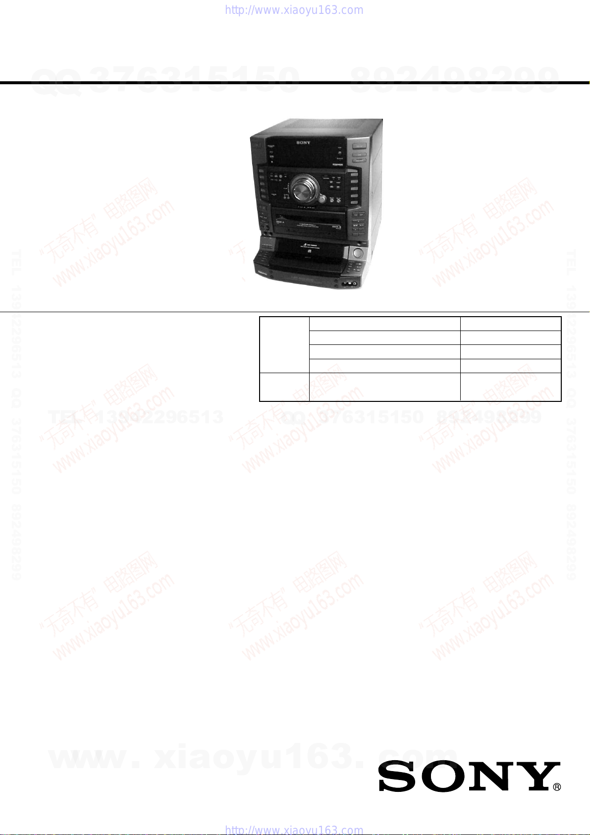
• HCD-XGV6/XGV8/XGV10AV are the
Amplifier, CD player, tape deck and
tuner section in LBT-XGV6/XGV8/
XGV10AV.
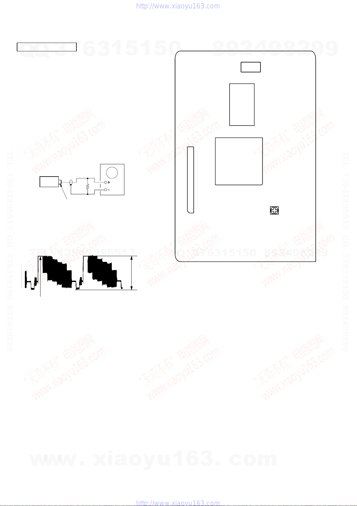
Photo : HCD-XGV10AV
Model Name Using Similar Mechanism NEW
CD CD Mechanism Type CDM37B-30BD62
Section Base Unit Name BU-30BD62
Optical Pick-up Name A-MAX.3
TAPE
Section
Model Name Using Similar Mechanism HCD-XGR90AV
8
9
2
4
9
8
2
9
E Model
9
TEL 13942296513 QQ 376315150 892498299
TEL
13942296513
Amplifier section
LBT-XGV10AV
Front Speaker:
The following measured at AC 120/220/240 V, 50 Hz
DIN power output (Rated) 150 + 150 watts
(6 ohms at 1 kHz, DIN)
Continuous RMS power output (Reference)
200 + 200 watts
(6 ohms at 1 kHz, 10% THD)
Center Speaker:
DIN power output (Rated) 35 watts
(8 ohms at 1 kHz, DIN)
Continuous RMS power output (Reference)
50 watts
(8 ohms at 1 kHz, 10% THD)
Rear Speaker:
DIN power output (Rated) 35 + 35 watts
(8 ohms at 1 kHz, DIN)
Continuous RMS power output (Reference)
50 + 50 watts
(8 ohms at 1 kHz, 10% THD)
LBT-XGV8
The following measured at AC 120/220/240V, 50 Hz
DIN power output (rated) 125W x 2 + 125W x 2
(6 ohms at 1 kHz, DIN)
Continuous RMS power output (reference)
170 W x 2 + 170 W x 2
(6 ohms at 1 kHz, 10% THD)
SPECIFICATIONS
Q
Q
6
7
3
LBT-XGV6
The following measured at AC 120/220/240V, 50 Hz
DIN power output (rated) 150 + 150 watts (6 ohms at 1 kHz, DIN)
Continuous RMS power output (reference)
Inputs
PHONO IN:
(phono jacks) sensitivity 3 mV,
MIC1/2:
(phone jacks) sensitivity 1 mV,
GAME INPUT:
(phono jacks) sensitivity 250 mV,
MD (VIDEO) IN:
(phono jack) sensitivity 450 mV
DVD INPUT (XGV10AV)
FRONT, REAR, CENTER, WOOFER (phono jacks):
COMPACT Hi-Fi STEREO SYSTEM
3
1
5
1
5
9
4
2
9
8
0
200 + 200 watts (6 ohms at 1 kHz,
10% THD)
impedance 47 kilohms
impedance 10 kilohms
impedance 47 kilohms
(250 mV),
impedance 47 kilohms
sensitivity 450 mV,
impedance 47 kilohms
— Continued on next page —
8
2
9
9
w
w
9-873-959-01
2002G0200-1
© 2002.07
w
.
xia
Sony Corporation
Home Audio Company
Published by Sony Engineering Corporation
o
y
u
1
6
3
.
c
o
m
HCD-XGV6/XGV8/XGV10AV
Outputs
PHONES:
Q
Q
(stereo phone jack) accepts headphones of 8 ohms or more
MD (VIDEO) OUT:
(phono jacks) voltage 250 mV
LBT-XGV10AV
WOOFER OUT (phono jack): voltage 1 V, impedance 1 kilohm
FRONT SPEAKER: accepts impedance of 6 to 16 ohms
CENTER SPEAKER: accepts impedance of 8 to 16 ohms
REAR SPEAKER: accepts impedance of 8 to 16 ohms
LBT-XGV8
FRONT SPEAKER: accepts impedance of 6 to 16 ohms
TEL 13942296513 QQ 376315150 892498299
LBT-XGV6
FRONT SPEAKER: accepts impedance of 6 to 16 ohms
Video section
Inputs
GAME INPUT (phono jack): 1 V p-p, 75 ohms
Outputs
VIDEO OUT (phono jack): 1 V p-p, 75 ohms
VIDEO CD/CD player section
System Compact disc and digital audio system
Laser Semiconductor laser
Frequency response 2 Hz – 20 kHz (±0.5 dB)
Signal-to-noise ratio More than 90 dB
Dynamic range More than 90 dB
TEL
Video color system format NTSC, PAL
Tape player section
Recording system 4-track 2-channel stereo
Frequency response 40 – 13,000 Hz (±3 dB),
Wow and flutter ±0.15% W.Peak (IEC)
Tuner section
FM stereo, FM/AM superheterodyne tuner
3
7
6
impedance 1 kilohms
(SUPER WOOFER)
accepts impedance of 6 to 16 ohms
(TWEETER & WOOFER)
(λ=795nm), Emission
duration: continuous
3
1
13942296513
using Sony TYPE I cassette
0.1% W .RMS (NAB)
±0.2% W .Peak (DIN)
5
1
5
Thai model: 220 V AC, 50/60 Hz
Other models: 120 V, 220 V or 230 –240 V AC,
0
Power consumption
LBT-XGV10AV 230 watts
LBT-XGV8 320 watts
LBT-XGV6 180 watts
Dimensions (w/h/d) Approx. 355 x 425 x 451 mm
Mass:
LBT-XGV10AV Approx. 15.4 kg
LBT-XGV8 Approx. 16.4 kg
LBT-XGV6 Approx. 14.7 kg
Supplied accessories: AM loop antenna (1)
Design and specifications are subject to change witho fi notice.
Notes on chip component replacement
• Never reuse a disconnected chip component.
• Notice that the minus side of a tantalum capacitor may be
damaged by heat.
Flexible Circuit Board Repairing
• Keep the temperature of soldering iron around 270˚C
Q
Q
during repairing.
• Do not touch the soldering iron on the same conductor of the
circuit board (within 3 times).
• Be careful not to apply force on the conductor when soldering
or unsoldering.
CAUTION
Use of controls or adjustments or performance of procedures
other than those specified herein may result in hazardous radiation
exposure.
3
7
8
6
3
4
2
9
50/60 Hz
Adjustable with voltage selector
FM lead antenna (1)
Speaker cords (XGV6, XGV8 (4),
XGV10AV (5))
Speaker pads (XGV6, XGV8 (8),
XGV10AV (12))
Remote commander (1)
Batteries (2)
Video connecting cable (1)
8
0
5
1
5
1
9
9
8
2
4
2
9
8
9
2
9
9
TEL 13942296513 QQ 376315150 892498299
9
FM tuner section
Tuning range 87.5 – 108.0 MHz
Antenna FM lead antenna
Antenna terminals 75 ohms unbalanced
Intermediate frequency 10.7 MHz
AM tuner section
Tuning range
Middle Eastern model: 531 – 1,602 kHz
Other models: 531 – 1,602 kHz
Antenna AM loop antenna
Antenna terminals External antenna terminal
Intermediate frequency 450 kHz
General
Power requirements
Saudi Arabian model: 120 – 127 V, 220 V or 230 – 240 V AC,
w
w
w
2
(50 kHz step)
(with the interval set at 9 kHz)
(with the interval set at 9 kHz)
530 – 1,710 kHz
(with the interval set at 10 kHz)
.
xia
50/60 Hz
Adjustable with voltage selector
o
y
This appliance is classified as a CLASS 1 LASER product. The
CLASS 1 LASER PRODUCT MARKING is located on the rear
exterior.
u
1
6
3
.
c
o
m
HCD-XGV6/XGV8/XGV10AV
SAFETY-RELATED COMPONENT WARNING!!
7
Q
Q
TEL 13942296513 QQ 376315150 892498299
TEL
w
3
COMPONENTS IDENTIFIED BY MARK 0 OR DOTTED LINE WITH
MARK 0 ON THE SCHEMATIC DIAGRAMS AND IN THE PARTS
LIST ARE CRITICAL TO SAFE OPERATION. REPLACE THESE
COMPONENTS WITH SONY PARTS WHOSE PART NUMBERS
APPEAR AS SHOWN IN THIS MANUAL OR IN SUPPLEMENTS
PUBLISHED BY SONY .
NOTES ON HANDLING THE OPTICAL PICK-UP
BLOCK OR BASE UNIT
The laser diode in the optical pick-up block may suffer electrostatic
break-down because of the potential difference generated by the
charged electrostatic load, etc. on clothing and the human body.
During repair, pay attention to electrostatic break-down and also
use the procedure in the printed matter which is included in the
repair parts.
The flexible board is easily damaged and should be handled with
care.
NOTES ON LASER DIODE EMISSION CHECK
The laser beam on this model is concentrated so as to be focused on
the disc reflective surface by the objective lens in the optical pickup block. Therefore, when checking the laser diode emission,
observe from more than 30 cm away from the objective lens.
LASER DIODE AND FOCUS SEARCH OPERATION
CHECK
Carry out the “S curve check” in “CD section adjustment” and
check that the S curve waveforms is output three times.
13942296513
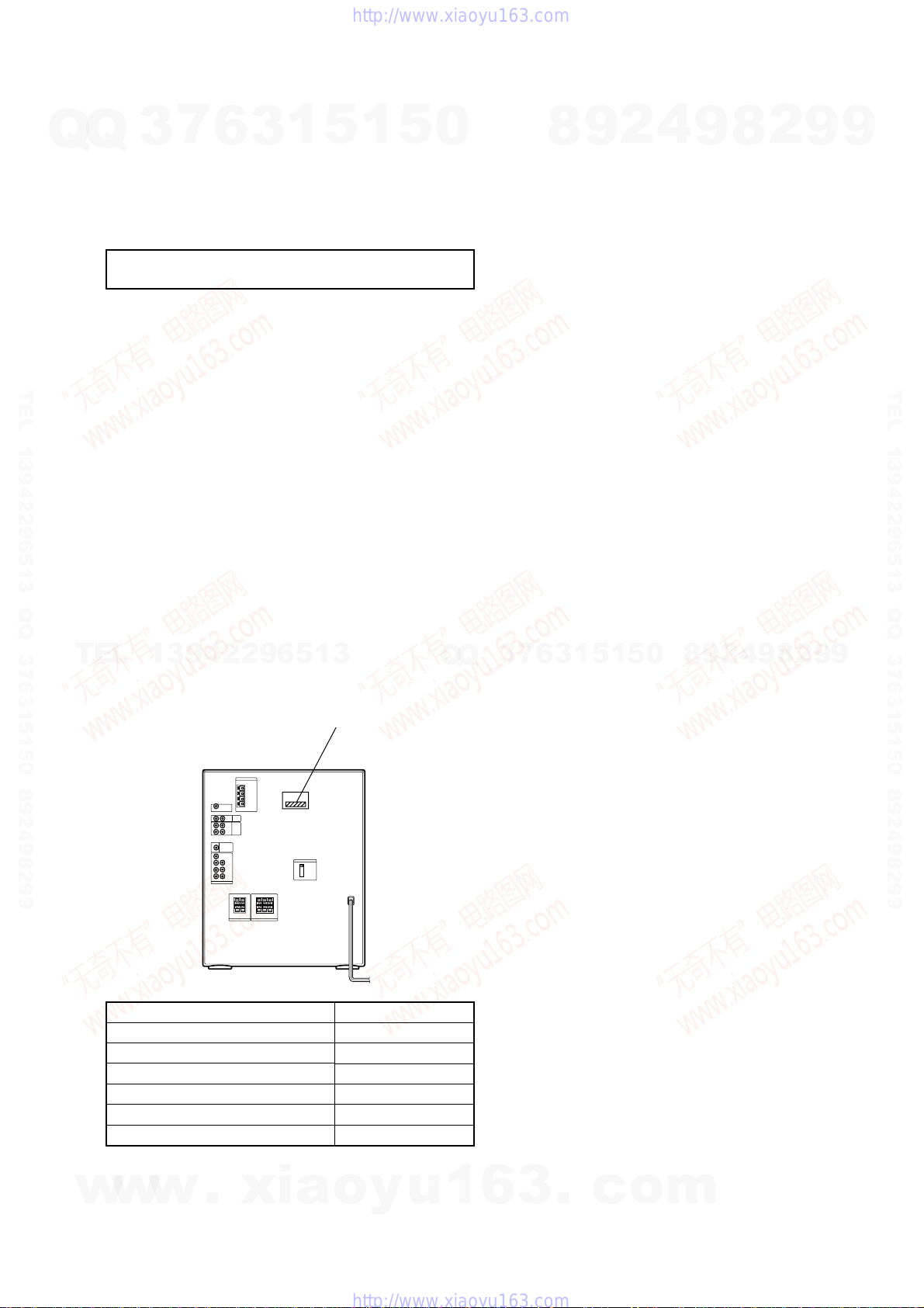
• MODEL IDENTIFICATION
– Rear Panel –
XGV10AV : SP model
XGV10AV : TH model
XGV8 : SP model
XGV6 : TH model
XGV6 : SP model
XGV10AV : EA model
• Abbreviation
SP : Singapore model
TH: Thai model
w
w
EA: Saudi Arabia model
6
MODEL
.
1
3
PART No.
xia
5
o
1
5
PARTS No.
4-238-825-2s
4-238-825-3s
4-238-825-4s
4-238-825-5s
4-238-825-6s
4-238-825-7s
y
u
0
Q
Q
1
1. SERVICING NOTE·························································· 4
2. GENERAL ·········································································· 5
3. DISASSEMBY···································································8
4. TEST MODE ···································································· 16
5. MECHANICAL ADJUSTMENTS ····························· 18
6. ELECTRICAL ADJUSTMENTS ·······························18
7. DIAGRAMS
7-1. Circuit Board Location ······················································23
7-2. Block Diagram – CD Servo Section – ······························· 24
– Display/Key Control/Power Supply Section –·········· 27
7-3. Printed Wiring Board – BD Section – ·······························28
7-4. Schematic Diagram – BD Section – ·································· 29
7-5. Schematic Diagram –Video (1/2) Section – ······················ 30
7-6. Schematic Diagram –Video (2/2) Section – ······················ 31
7-7. Printed Wiring Board – Video Section – ···························32
7-8. Printed Wiring Board – Motor, LED Section – ················· 33
7-9. Schematic Diagram –Motor, LED Section – ····················· 33
7-10.Schematic Diagram – Main (1/3) Section – ······················34
7-11.Schematic Diagram – Main (2/3) Section – ······················35
7-12.Schematic Diagram – Main (3/3) Section – ······················36
7-13.Printed Wiring Board – Main Section – ····························37
7-14.Printed Wiring Board
– CD-L,CD-R,Headphone,Front Input,D-SW Section –··38
7
3
7-15.Schematic Diagram
– CD-L,CD-R,Headphone,Front Input,D-SW Section –··39
7-16.Printed Wiring Board – Panel VR Section – ······················ 40
7-17.Schematic Diagram – Panel VR Section – ························ 41
7-18.Printed Wiring Board – Panel FL,TC-A,TC-B Section –·42
7-19.Schematic Diagram – Panel FL,TC-A,TC-B Section –·····43
7-20.Printed Wiring Board – PA Section (XGV10AV) – ··········· 44
7-21.Schematic Diagram – PA Section (XGV10AV) – ············· 45
7-22.Printed Wiring Board – PA Section (XGV6/XGV8) – ······ 46
7-23.Schematic Diagram – PA Section (XGV6/XGV8) –········· 47
7-24. Schematic Diagram – Sub Amp Section (XGV10AV) –··48
7-25. Schematic Diagram – Sub Amp Section (XGV8) –··········49
7-26.Printed Wiring Board
– Sub Amp Section (XGV10AV/XGV8) – ························· 50
7-27.Schematic Diagram – MIC/Guitar Section –····················· 51
7-28.Printed Wiring Board – MIC/Guitar Section – ·················· 51
7-29.Printed Wiring Board – Prologic Section (XGV10AV) –··52
7-30.Schematic Diagram – Prologic Section (XGV10AV) – ····53
7-31. Printed Wiring Board – T rans,Sub T rans Section – ·········· 54
7-32.Schematic Diagram – Trans,Sub T rans Section –··············55
7-33. IC Pin Function Description ············································· 56
7-34. IC Block Diagram ····························································· 63
8. EXPLODED VIEWS
8-1. Case,Back Panel Section ··················································· 66
8-2. Front Panel Section-1 ························································ 67
8-3. Front Panel Section-2 ························································ 68
8-4. Chassis Section ·································································· 69
8-5. CD Mechanism Deck Section
(CDM37B-30BD62)··························································· 70
8-6. Base Unit Section (BU-30BD62) ······································71
9. ELECTRICAL PARTS LIST ······································· 72
6
3
TABLE OF CONTENTS
4
2
9
8
Block Diagram – Tuner/Tape Deck Section – ··················· 25
Block Diagram – Main Section – ······································ 26
Block Diagram
0
5
1
5
1
3
6
.
c
o
9
9
8
m
2
8
4
2
9
8
9
2
9
9
9
TEL 13942296513 QQ 376315150 892498299
3
HCD-XGV6/XGV8/XGV10AV
JIG FOR CHECKING PROLOGIC BOARD (XGV10AV ONLY)
7
Q
Q
The special jig (J-2501-216-A) is useful for checking the PROLOGIC board.
3
6
PROLOGIC board
3
1
CN201
5
SECTION 1
SERVICING NOTE
1
5
0
8
9
2
4
9
MAIN board
8
2
9
9
TEL 13942296513 QQ 376315150 892498299
CN202
Jig (J-2501-216-A)
CN151
TEL
13942296513
Q
Q
3
7
6
CN152
1
3
5
1
5
0
8
9
2
4
9
8
2
9
TEL 13942296513 QQ 376315150 892498299
9
4
w
w
w
.
xia
o
y
u
1
6
3
.
c
o
m
Q
Q
Main unit
7
3
6
3
ALPHABETICAL ORDER
1
SECTION 2
GENERAL
5
1
5
0
8
HCD-XGV6/XGV8/XGV10AV
This section is extracted from
instruction manual.
9
2
4
9
8
2
9
9
A — D
A EJECTZ/ Z B EJECT wl
ALBUM +/— ed
CD SYNC ql
Direct equalizer qh r;
POP/ROCK/JAZZ/DANCE/
GAME
SALSA/REGGAE/TANGO/
TEL 13942296513 QQ 376315150 892498299
TEL
SAMBA/MOVIE
DIRECTION ek
DISC SKIP eg
DISC 1 to 5 es
DISPLAY 2
DSP ra (XGV10AV)
DVD 5.1CH wg (XGV10AV)
1
13942296513
ra
E — K
ECHO LEVEL ej
EDIT ef
EFFECT 5
ENTER 5
FM MODE 8
FUNCTION qd
GAME qf
GAME INPUT AUDIO L/R jacks
wf
GAME INPUT VIDEO jack wf
GAME MIXING qg
GROOVE ra
H SPEED DUB ql
KARAOKE PON/MPX ea
KEY CONTROL #/ 2 ea
234 5 76 890 qa qs
7
3
Q
Q
6
3
1
M — R
MIC LEVEL ej
MIC 1/2 jacks eh
NEXT wd
P FILE 5
PHONES jack w;
PICTURE EFFECT wd
PLAY MODE eg
POWER SAVE/DEMO
(STANDBY) 3
Power stream indicator 6
PREV wd
PRO LOGIC wg (XGV10AV)
PUSH OPEN wk
REPEAT eg
RETURN O wd
qd
9
8
0
5
1
5
qf
qg
2
4
9
8
2
9
TEL 13942296513 QQ 376315150 892498299
9
w
w
w
.
xia
r;
el
ek
ej
eh
eg
ef
o
y
u
1
wk
6
3
.
wfwgwhwjwle;eaesed
c
o
qh
qj
qk
ql
w;
wa
ws
wd
m
5
HCD-XGV6/XGV8/XGV10AV
This section is extracted from
instruction manual.
S — X
Q
Q
SELECT wd
SLEEP 0
SPECTRUM ANALYZER 4
SUPER WOOFER ra
SUPER WOOFER MODE ra
SURROUND (XGV6, XGV8) ra
TIMER SELECT qa
TUNER/BAND 9
TUNER ENTER wh
TUNER MEMORY wh
TUNING MODE 8
TUNING —/+ 9
TEL 13942296513 QQ 376315150 892498299
VOLUME control 7
X-GROOVE wj
BUTTON DESCRIPTIONS
@/1 1
c/CLOCK SET qs
h/H qj el
x qj el
.m /M> qj el
X qk
z REC qk
.AMS> wa
HX ws
x ws
m /M ws
R/r/T/t (cursor) e;
TEL
3
7
6
3
1
13942296513
Remote control
5
1
5
0
ALPHABETICAL ORDER
A—E
ALBUM +/— eg
CD N wl
CENTER LEVEL +/— w;
CLEAR 6
CLOCK/TIMER SELECT r;
CLOCK/TIMER SET 1
DISC SKIP ef
DISPLAY eh
DSP wh
DVD 5.1CH wg
EFFECT q;
ENTER ws
F—R
FILE SELECT +/— qf
FUNCTION +/— ea
KEY CONTROL #/ 2 ql
NEXT wj
Numeric buttons ej
ON SCREEN ek
PICTURE EFFECT 9
PLAY MODE ed
PRESET —/+ wj
PREV wj
PRO LOGIC wf
REAR LEVEL +/— qh
REPEAT es
RETURN O qa
Q
Q
3
7
(For XGV10AV)
2
9
8
S—V
SELECT wl
SLEEP el
SPECIAL MENU 8
TAPE A nN e;
TAPE B nN qg
TEST TONE wd
TUNER/BAND wk
TUNING —/+ qj
TV CH +/— 5
TV/VIDEO 7
TV VOL +/— 4
TV @/1 2
VOL +/— qk
BUTTON DESCRIPTIONS
@/1 3
X qs
x qd
m /M qj
R/r/T/t (cursor) wa
./> wj
1
3
6
r;
el
ek
ej
eh
eg
ef
ed
es
ea
e;
wl
wk
wj
wh
wg
wf
wd
ws
5
1
5
0
4
9
8
9
8
2
4
9
1
2
3
4
5
6
7
8
9
0
qa
qs
qd
qf
qg
qh
qj
qk
2
8
9
2
9
9
TEL 13942296513 QQ 376315150 892498299
9
6
w
w
w
.
xia
o
y
u
1
6
3
wa
.
c
o
ql
w;
m
HCD-XGV6/XGV8/XGV10AV
This section is extracted from
instruction manual.
7
Q
Q
TEL 13942296513 QQ 376315150 892498299
TEL
3
13942296513
6
Remote control
1
5
1
3
ALPHABETICAL ORDER
A—F
ALBUM +/— es
CD N wh
CLEAR 6
CLOCK/TIMER SELECT ej
CLOCK/TIMER SET 1
DISC SKIP ea
DISPLAY ed
EFFECT qf
ENTER wa
FILE SELECT +/— 9
FUNCTION +/— wk
G—R
GROOVE ws
KEY CONTROL #/ 2 ql
NEXT wd
Numeric buttons ef
ON SCREEN eg
PICTURE EFFECT wf
PLAY MODE e;
PRESET —/+ wd
PREV wd
REPEAT wl
RETURN O q;
5
(F or XGV6, XGV 8 )
0
S—V
SELECT wh
SLEEP eh
SPECIAL MENU 8
SUPER WOOFER qj
SURROUND qg
TAPE A nN wj
TAPE B nN qd
TUNER/BAND wg
TUNING —/+ qh
TV CH +/— 5
TV/VIDEO 7
TV VOL +/— 4
TV @/1 2
VOL +/— qk
BUTTON DESCRIPTIONS
@/1 3
X qa
x qs
m /M qh
R/r/T/t (cursor) w;
7
3
Q
Q
./> wd
ej
eh
8
6
3
9
1
5
2
1
5
4
0
9
8
1
2
9
8
2
4
2
9
8
9
2
9
9
TEL 13942296513 QQ 376315150 892498299
9
w
w
w
.
xia
o
y
u
1
eg
ef
ed
es
ea
e;
wl
wk
wj
wh
wg
wf
wd
ws
wa
w;
6
3
.
c
o
3
4
5
6
7
8
9
0
qa
qs
qd
qf
qg
qh
qj
qk
ql
m
7
)
HCD-XGV6/XGV8/XGV10AV
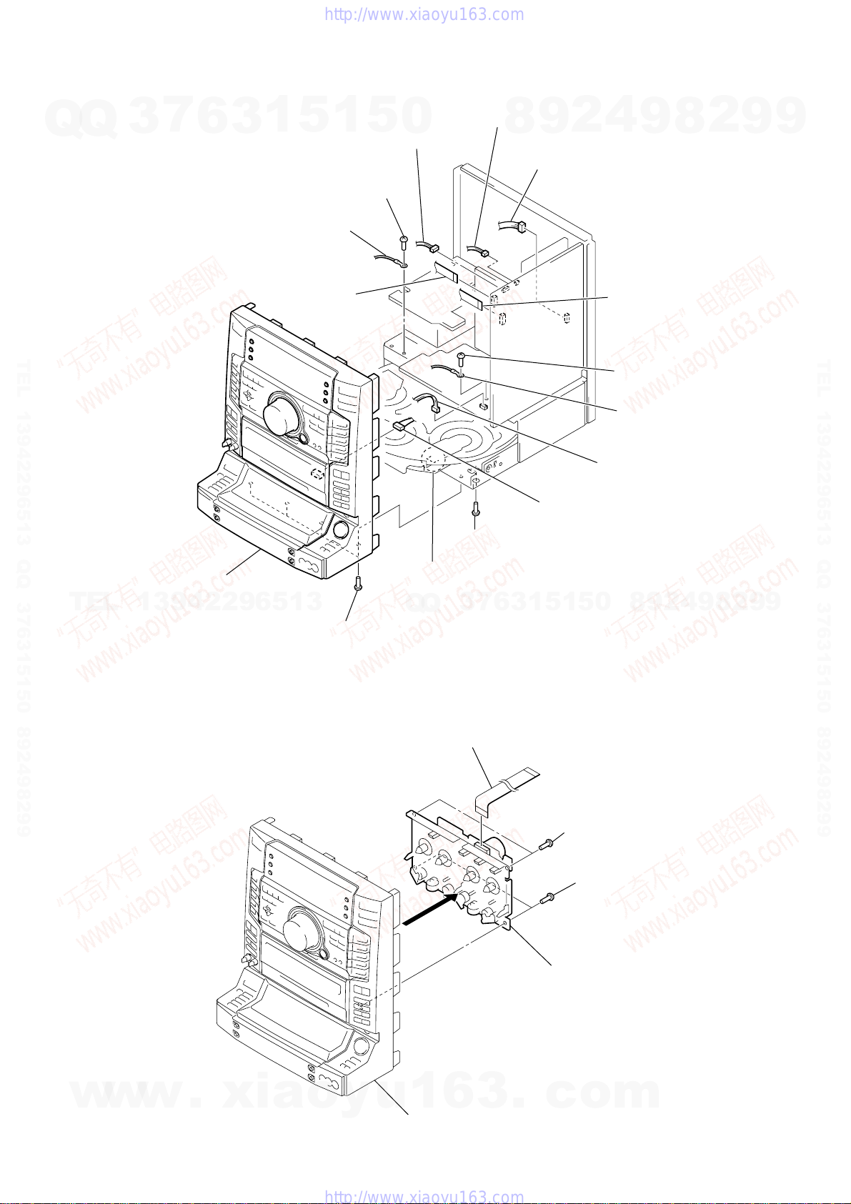
SECTION 3
DISASSEMBLY
• The equipment can be removed using the following procedure.
Q
7
Q
3
Set Case Front panel section Tape mechanism deck
6
3
1
5
1
5
0
PANEL FL board, TC-A board, TC-B board
PANEL VR board
MIC/GUITAR board, HEADPHONE board
FRONT INPUT board
8
9
2
4
9
8
2
9
9
TEL 13942296513 QQ 376315150 892498299
Back panel, DC fan, MAIN board, PROLOGIC board (XGV10), VIDEO board
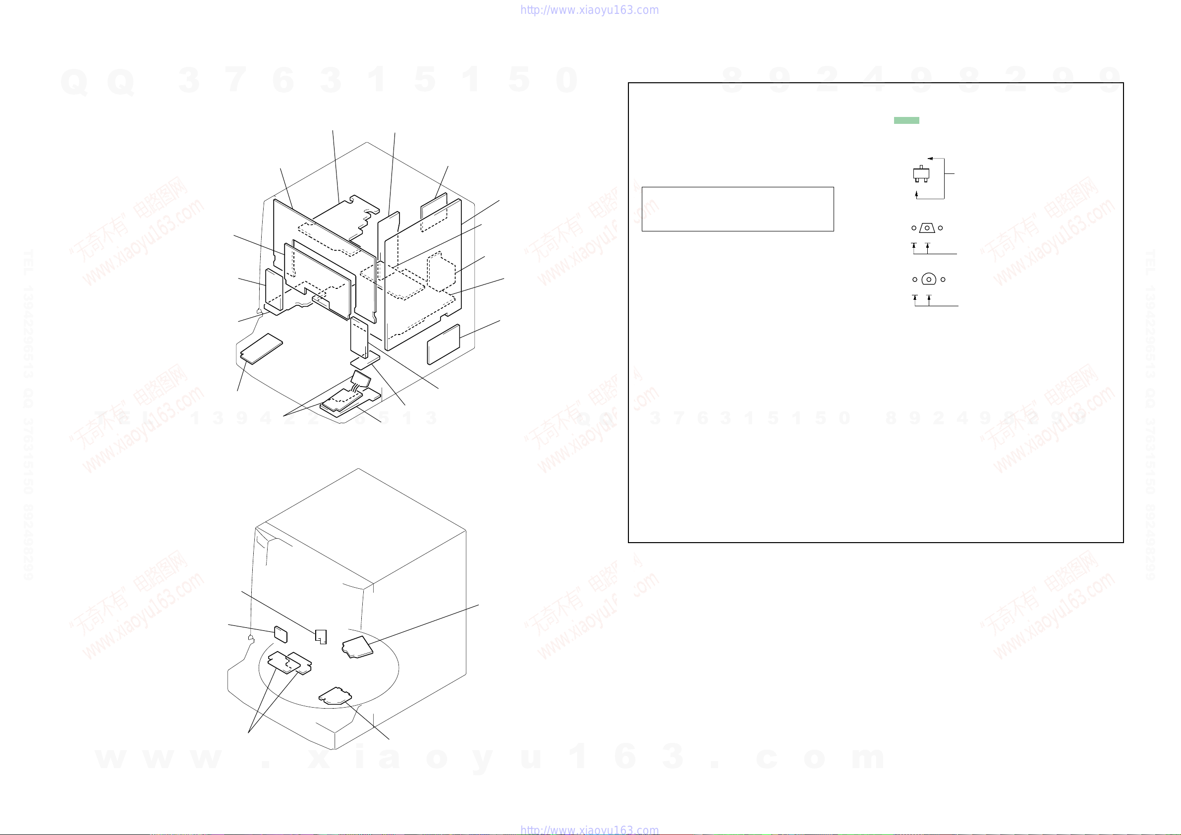
CD mechanism deck (CDM37B-30BD62)
Base unit-1 (BU-30BD62)
Disc table
Note : Follow the disassembly procedure in the numerical order given.
3-1. CASE
TEL
13942296513
8
Case
7
D-SW board, CD-L board, Lid (CD) assy, CD-R board
Base unit-2 (BU-30BD62) BD board
7
3
Q
Q
3
Five screws (BVTT 3
6
3
1
5
×
1
TEL 13942296513 QQ 376315150 892498299
9
9
2
8
9
4
2
9
8
0
5
6)
8
w
w
1
Three screws
(CASE3 TP2)
w
.
6
xia
5
6
o
y
u
1
6
4
Two screws (BVTP 3
5
2
Three screws (CASE3 TP2)
3
.
c
o
m
×
8
)
k
HCD-XGV6/XGV8/XGV10AV
3-2. FRONT PANEL SECTION
7
Q
Q
TEL 13942296513 QQ 376315150 892498299
3
6
1
3
2
Flat type wire (CN431)
5
7
Screw (BVTP 3 X 8)
8
1
Lug
5
0
3
Connector (CN311)
4
Connector (CN903)
2
9
8
5
Connector (CN722)
qa
Connector (B deck)
4
1
Flat type wire
(CN371)
9
Screw (BVTP 3 X 8
0
Lug
6
Connector (CN806)
9
8
2
9
9
TEL 13942296513 QQ 376315150 892498299
qg
Front panel section
TEL
13942296513
3-3. TAPE MECHANISM DECK
qd
Four screws (BVTP 3 X 8)
qs
Screw (BVTP 3 X 8)
qf
Claw
6
7
3
Q
Q
1
Flat type wire (15 core)
4
3
1
5
1
2
(BVTP 2.6 X 8)
9
8
0
5
Two screws
3
Two screws
(BVTP 2.6 X 8)
2
4
9
8
2
9
9
w
w
w
.
xia
o
y
u
1
6
Front panel
3
.
5
Tape mechanism dec
c
o
m
9
y
HCD-XGV6/XGV8/XGV10AV
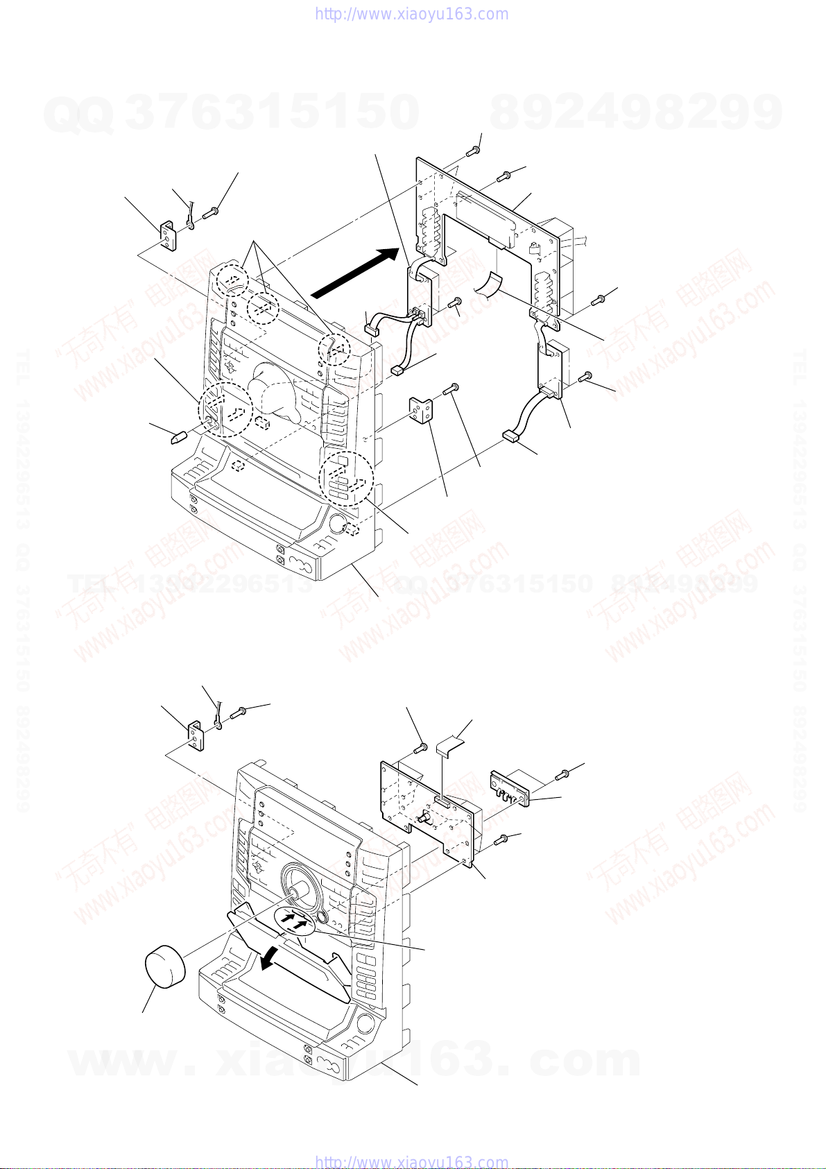
3-4. PANEL FL BOARD, TC-A BOARD, TC-B BOARD
Q
Q
3
Bracket (TA)
3
7
6
1
Screw (BVTP 2.6 X 8)
2
Lug
1
3
qh
Three claws
5
1
w;
5
TC-A board
0
qa
Five screws (BVTP 2.6 X 8)
2
9
8
qs
Three screws
(BVTP 2.6 X 8)
qk
PANEL FL board
4
9
8
2
9
9
qj
6
Connector
(CN812)
qf
Four screws
TEL 13942296513 QQ 376315150 892498299
TEL
3-5. PANEL VR BOARD
ql
Two claws
0
Two knobs (MIC)
13942296513
Q
Front panel
(BVTP 2.6 X 8)
7
Connector
(CN704)
5
wa
Two claws
3
Q
Bracket (TA)
7
8
4
Screw
(BVTP 2.6 X 8)
3
6
Connector (CN703)
1
5
1
qd
Eight screws
(BVTP 2.6 X 8)
9
(CN601)
ws
TC-B board
8
0
5
Flat type wire
qg
Four screws
(BVTP 2.6 X 8)
9
4
2
9
8
2
9
TEL 13942296513 QQ 376315150 892498299
9
4
w
w
3
Bracket (TA)
Knob (VOLUME)
w
.
2
Lug
xia
1
Screws
(BVTP 2.6 X 8)
7
o
y
0
Eight screws
(BVTP 2.6 X 8)
6
u
1
6
Front panel
5
Flat type wire
(CN701)
8
(BVTP 2.6 X 8)
9
Lever (EJECT) ass
qa
Nine screws
(BVTP 2.6 X 8)
c
o
qs
PANEL VR board
Preess the two buttons (EJECT)
3
.
Two screws
m
10
t
)
Q
3-6. MIC/GUITAR BOARD, HEADPHONE BOARD
Q
3
7
6
3
1
5
1
5
0
1
(CN812)
Connector
9
8
4
MIC/GUITAR board
HCD-XGV6/XGV8/XGV10AV
4
2
2
Two screws
(BVTP 2.6 X 8)
3
MIC bracket
9
8
2
9
9
TEL 13942296513 QQ 376315150 892498299
Front panel
TEL
13942296513
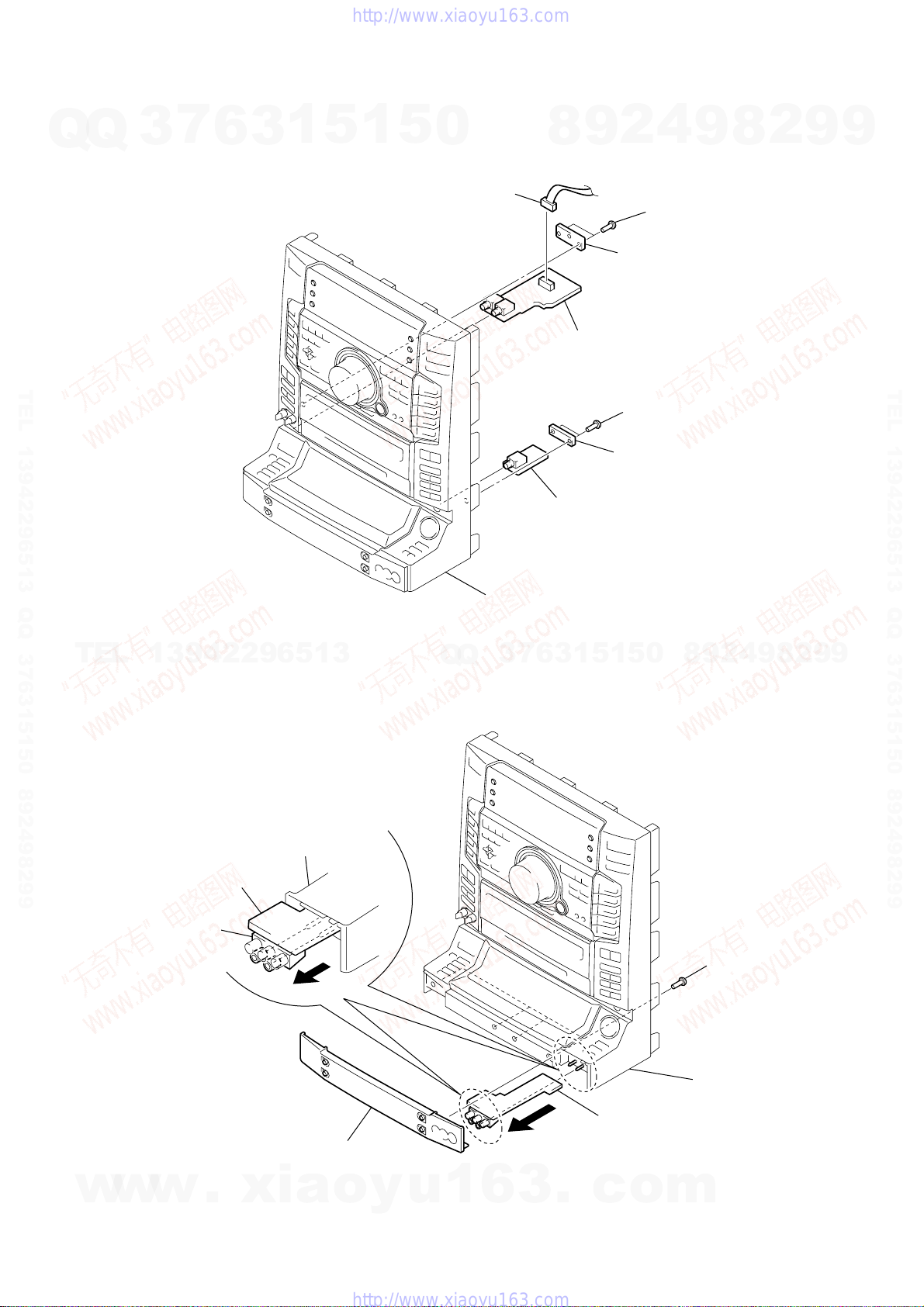
3-7. FRONT INPUT BOARD
Q
Q
3
7
7
HEADPHONE board
5
1
3
6
5
Two screws
(BVTP 2.6 X 8)
6
HEADPHONE bracke
9
8
0
5
1
2
4
9
8
2
9
TEL 13942296513 QQ 376315150 892498299
9
w
w
FRONT INPUT board
J804
w
.
Front panel
2
Bumper (Panel)
xia
o
y
u
1
6
3
3
.
4
FRONT INPUT board
c
o
m
1
Four screws
(BVTP 2.6 X 8
Front panel
11
d
)
HCD-XGV6/XGV8/XGV10AV
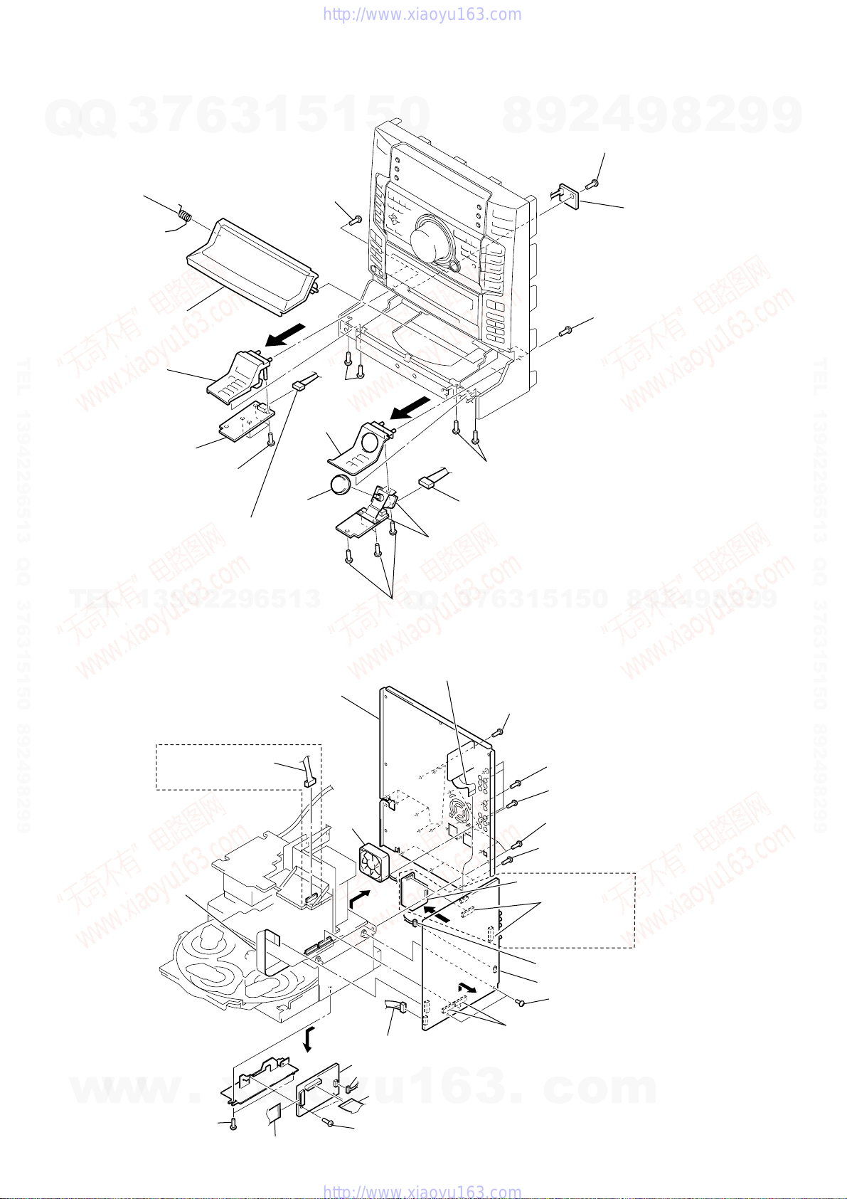
3-8. D-SW BOARD, CD-L BOARD, LID (CD) ASSY, CD-R BOARD
7
Q
Q
TEL 13942296513 QQ 376315150 892498299
3
0
Spring (CD)
qa
Lid (CD) assy
9
Sub panel (CD-L) assy
6
3
1
5
5
Two screws
(BVTP 2.6 X 8)
6
4
(BVTP 2.6 X 8)
ql
Sub panel
(CD-R) assy
1
5
Two screws
0
qh
8
4
2
9
1
Screw (BVTP 2.6 X8)
qf
(BVTP 2.6 X 8)
9
2
D-SW boar
Two screws
8
2
9
9
TEL 13942296513 QQ 376315150 892498299
8
CD-L board
qg
7
Four screws
(BVTP 2.6 X 8)
qd
Knob
3
Connector
(CN704)
TEL
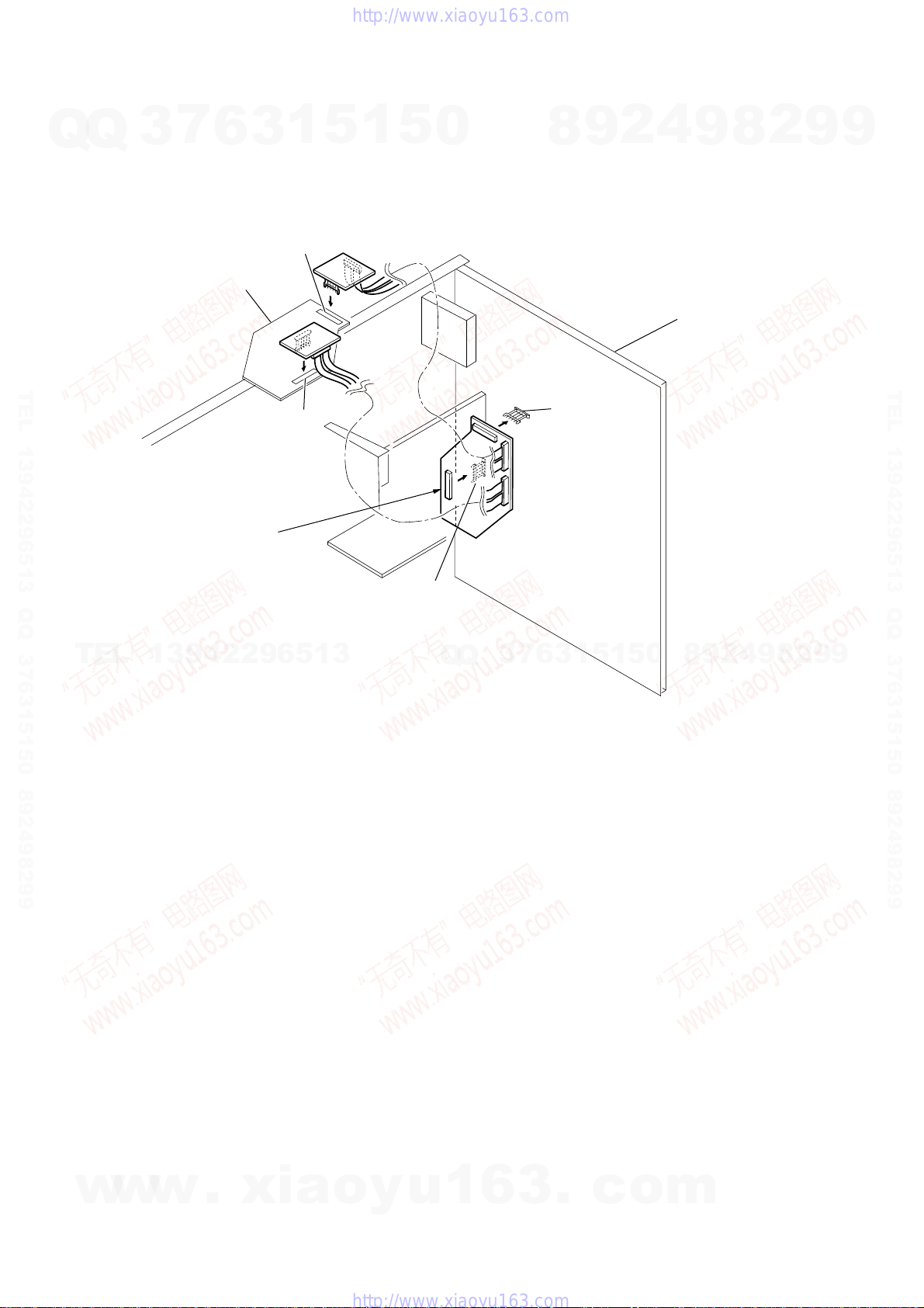
3-9. BACK PANEL, DC FAN, MAIN BOARD, PROLOGIC BOARD (XGV10), VIDEO BOARD
13942296513
qd
Connector (CN102)
XGV8/XGV10
qa
Flat type wire
(CN401)
(CD)
7
Back panel
q;
DC FAN
(M901)
qj
Four screws
Q
(BVTP 2.6 X 8)
1
6
qk
CD-R board
Q
Flat type wire (CN441)
qk
Two screws
(BVTP 2.6 X 8)
qs
Connector (CN703)
1
3
6
7
3
2
Eight screws
(BVTP 3 X 8)
ql
PROLOGIC board
0
5
1
5
3
Four screws
(BVTP 3 X 8)
9
(BVTP 3 X 8)
5
(BVTP 3 X 8)
4
(BVTP 3 X 8)
qj
(CN151, 152)
Two screws
Four screws
Three screws
Two connectors
8
9
2
4
9
8
2
9
9
12
w
w
w
.
w;
Two screws
(BVTP 3 X 8)
xia
wd
Flat type wire
(CN201)
wa
qs
Connector (CN441)
wh
VIDEO board
wf
Connector (CN301)
Flat type wire (CN101)
o
ws
y
u
wg
Two screws
(BVTP 3 X 8)
1
6
3
8
Connector (CN961
qh
MAIN board
qf
qg
(CN901, 902)
.
Two screws
(BVTP 3 X 8)
Two connectors
c
XGV10
o
m

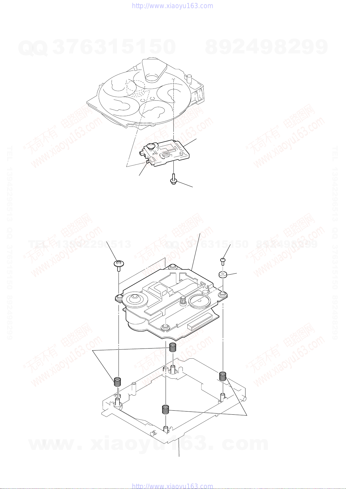
3-10. CD MECHANISM DECK (CDM37B-30BD62)
7
Q
Q
TEL 13942296513 QQ 376315150 892498299
3
6
4
(BVTP 3 X 8)
1
3
Three screws
5
1
(CN401)
1
5
Flat type wire
7
0
6
Two screws (BVTP 3 X 8)
8
HCD-XGV6/XGV8/XGV10AV
9
4
2
3
Four screws (BVTP 3 X 8)
9
8
2
9
9
TEL 13942296513 QQ 376315150 892498299
TEL
2
Connector
(CN411)
13942296513
0
Five screws
(BVTP3 × 8)
Q
8
Q
3
7
6
7
3
1
5
Two screws
(BVTP 3 X 8)
5
1
5
Wire holder
9
Remove two cables from
wire holder.
4
2
9
8
0
9
8
2
9
9
w
w
qa
CD mechanism deck
(CDM37B-30BD62)
w
.
xia
o
y
u
1
6
3
.
c
o
m
13
w
)
HCD-XGV6/XGV8/XGV10AV
3-11. BASE UNIT-1 (BU-30BD62)
7
Q
Q
TEL 13942296513 QQ 376315150 892498299
3
6
3
1
5
1
5
0
3
9
8
Base unit
(BU-30BD62)
2
4
9
8
2
9
9
TEL 13942296513 QQ 376315150 892498299
3-12. BASE UNIT-2 (BU-30BD62)
1
Two floating screws (DIA.12)
TEL
13942296513
2
Boss
1
6
Base unit (BU-30BD62)
7
3
Q
Q
BU fitting scre
5
1
3
6
2
Two screws
5
1
(BVTP 2.6 X 8)
3
(BU)
8
0
Two stoppers
9
2
4
9
8
2
9
9
14
w
w
4
Two coil springs
(insulator)
w
.
xia
o
y
u
1
6
3
Holder (BU30) assy
.
c
o
5
Two coil
springs
(insulator
m
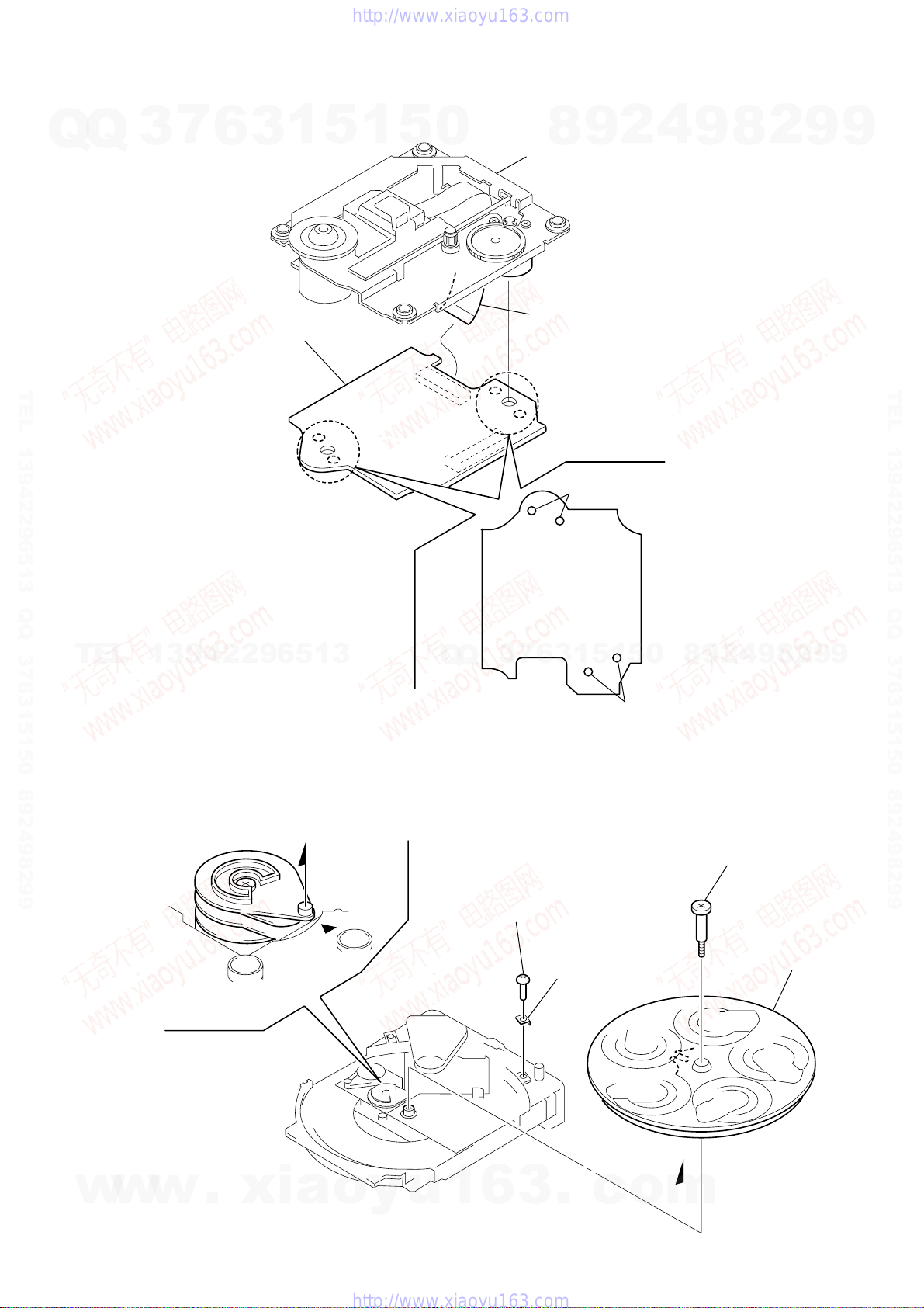
e
Q
3-13. BD BOARD
Q
3
7
6
3
4
1
5
BD board
1
5
0
8
BU-30BD62
3
Flat type wire (CN102)
HCD-XGV6/XGV8/XGV10AV
9
2
4
9
8
2
9
9
TEL 13942296513 QQ 376315150 892498299
TEL
13942296513
3-14. DISC TABLE
Note: When the disc table is installed, adjust the positions of roller cam
and mark B as shown in the figure, then set to the groove of disc
table.
A
Q
Q
3
7
1
Remove the two solders.
1
5
1
3
6
2
Remove the two solders.
5
0
8
9
2
4
9
8
2
9
TEL 13942296513 QQ 376315150 892498299
9
w
w
w
.
xia
1
Screw (BVTP 3
o
y
u
1
6
3
×
8)
2
Bracket (BU)
.
c
o
m
A
3
Step screw
4
Disc tabl
15
HCD-XGV6/XGV8/XGV10AV
B
SECTION 4
TEST MODE
[MC Cold Reset]
• The cold reset clears all data including preset data stored in the
Q
Q
RAM to initial conditions. Execute this mode when returning
the set to the customer.
Procedure:
1.Turn the power ON or set to the DEMO mode.
2.Press three buttons of c/CLOCK SET , TUNER ENTER , and
\/1 simultaneously.
3. The set is reset, and displays “COLD RESET”, then becomes
DEMO mode.
[Change-over the AM Tuning Interval]
• The AM tuning interval can be changed over 9 kHz or 10 kHz.
Procedure:
1.Press the \/1 button to turn the power ON.
2.Select the function “TUNER”, and press the TUNER/BAND
button to select the BAND “AM”.
TEL 13942296513 QQ 376315150 892498299
3. Press the \/1 button to turn the power OFF.
4. Press the ENTER/NEXT and \/1 buttons simultaneously,
and the display on the fluorescent indicator tube changes to
“AM 9 K STEP” or “AM 10 K STEP”, and thus the tuning
interval is changed over.
[CD Ship Mode] (No memory clear)
• This mode moves the optical pick-up to the position durable to
vibration. Use this mode when returning the set to the customer
after repair.
Procedure:
1.Press the \/1 button to turn the power ON.
2. Press the EDIT and
3. A message “LOCK” is displayed on the fluorescent indicator
tube, and the CD delivery mode is set.
TEL
[LED and Fluorescent Indicator Tube All Lit, Key Check
Mode]
Procedure:
1. Press three buttons of c/CLOCK SET , ENTER/NEXT ,
and DISC 2 simultaneously.
2. LEDs and fluorescent indicator tube are all turned on.
3.Press the DISC 1 button, the MODE and DESTINATION are
displayed fluorescent indicator tube.
4.Each time the DISC 1 button is pressed, the MC/GC category
version is displayed in the following order.
5.Press the DISC 2 button, and the key check mode is acti-vated.
NR MC GC CD CDDM CDMA
6. In the key check mode, the fluorescent indicator tube displays
“K 0 J0 V0”. Each time a button is pressed, “K” value in-creases
to “K69”call the button is pressed.However, once a button is
pressed, it is no longer taken into account.
“J” value increases like 1, 2, 3 ... if turn the . AMS > JOG
dial clock-wise,or it decreases like 0, 9, 8 ... if turn the
. AMS > JOG dial counter-clockwise.
“V” value increases like 1, 2, 3 ... if turn the VOLUME dial
clockwise (“+” direction), or it decreases like 0, 9, 8 ... if turn the
VOLUME dial counterclockwise (“–” direction).
7. To release from this mode, press three buttons in the same
manner as step 1, or disconnect the power cord.
3
7
6
buttons simultaneously.
\/1
3
1
13942296513
BDABDBSTTATMTC
5
1
CDM
5
[Sled Servo Mode] (CD service mode)
• This mode can run the CD sled motor freely. Use this mode, for
0
instance, when cleaning the pick-up.
Procedure:
1. Select the function “CD”.
2. Press three buttons c/CLOCK SET , TUNER ENTER , and
DISC 5 simultaneously.
3. The Sled Servo mode is selected, if “CD” is blanking on the
fluorescent indicator tube.
4. With the CD in stop status, press M button in CD section to
move the pick-up to outside track, or m button to inside track.
5. T o exit from this mode, press
Note:
• Always move the pick-up to most inside track when exiting from
this mode. Otherwise, a disc will not be unloaded.
• Do not run the sled motor excessively, otherwise the gear can be
chipped.
[Change-over of FUNCTION Name]
• The FUNCTION name of external input terminal can be changed
over to VIDEO or MD. W ith the FUNCTION selected to “MD”,
about 5dB mute is applied to the input gain.
Procedure:
1. Press \/1 button to turn the power OFF.
2. Press
several seconds, and the power is turned on, the display of
fluorescent indicator tube changes to “MD” or “VIDEO”
instantaneously, and thus the FUNCTION is changed over.
[Aging Mode]
This mode can be used for operation check of tape deck section.
Tape deck section work in parallel.
• If an error occurred:
Q
Q
The aging operation stops and display then status.
• If no error occurs:
The aging operation continues repeatedly.
Procedure:
1.Load the tapes into the decks A and B respectively.
2.Press the FUNCTION button to select the function “CD”.
3.Press the PLAY MODE button to set the “ALL DISCS” mode,
and press the REPEAT button to “REPEAT” off.
4. Press three buttons of c/CLOCK SET , TUNER ENTER ,
and DISC 4 simultaneously.
5. The aging mode is activated, if the indicator of disc tray number on the fluorescent indicator tube is blinking.
6. To release from the aging mode, press the \/1 button to turn
the power OFF and operate the cold reset. (Refer to the “MC
Cold Reset”)
1. Display at the Aging Mode
• Display operating state of tape deck section alternately.
• If an error occurred, stop display.
button together with FUNCTION button for
\/1
7
3
8
6
3
9
1
5
4
2
1
\/1
5
0
9
button turn to the power OFF .
2
9
8
8
4
2
9
8
9
2
9
9
TEL 13942296513 QQ 376315150 892498299
9
16
w
w
w
.
xia
o
y
u
1
6
3
.
c
o
m
HCD-XGV6/XGV8/XGV10AV
2. Tape Deck Section
Q
TEL 13942296513 QQ 376315150 892498299
• The sequence during the aging mode is following as below.
Q
• If an error occurred, stop display that step.
Aging mode sequence (Tape deck section):
7
3
Rewind the tape A
Fast forward the tape A
Rewind the tape A
6
“T APE A AG-1”
Shut off
FWD the tape A
“T APE A AG-2”
2 minutes
“T APE A AG-3”
Shut off or 20 seconds
RVS the tape A
“T APE A AG-4”
2 minutes
“T APE A AG-5”
Shut off
3
1
5
1
5
0
3. CD Section
• The sequence during the aging mode is following as below.
• If an error occurred, stop display that step.
Aging mode sequence (CD section):
9
8
TOC Read
Track 1 Play
Last Track Play
2
Tray Turn
DISC 1
chucking
4
2 seconds
2 seconds
9
8
2
9
9
TEL 13942296513 QQ 376315150 892498299
FWD the tape B
“TAPE B AG-2”
TEL
13942296513
Fast forward the tape B
“TAPE B AG-3”
RVS the tape B
“TAPE B AG-4”
Rewind the tape B
“TAPE B AG-5”
Note: “TAPE * AG- * ” is display of each step.
2 minutes
Shut off or 20 seconds
2 minutes
Shut off
Q
Q
Tray T un
9
2
8
9
4
2
9
8
0
5
1
5
1
3
6
7
3
DISC 4
Chucking
TOC Read
Track 1 Play
2 seconds
Last Track play
[VACS ON/OFF]
• The volume control by VACS is turned ON/OFF.
Procedure:
1.Press the \/1 button to turn the power ON.
2.Press the PLAY MODE and \/1 buttons simultaneously.
3.The reaction display appears when switcing ON/OFF.
9
w
w
w
.
xia
o
y
u
1
6
3
.
c
o
m
17
HCD-XGV6/XGV8/XGV10AV
SECTION 5
MECHANICAL ADJUSTMENTS
Precaution
1. Clean the following parts with a denatured alcohol-moistened
Q
Q
swab:
record/playback heads pinch rollers
erase head rubber belts
capstan idlers
2. Demagnetize the record/playback head with a head demagnetizer.
3. Do not use a magnetized screwdriver for the adjustments.
4. After the adjustments, apply suitable locking compound to the
parts adjusted.
5. The adjustments should be performed with the rated power supply voltage unless otherwise noted.
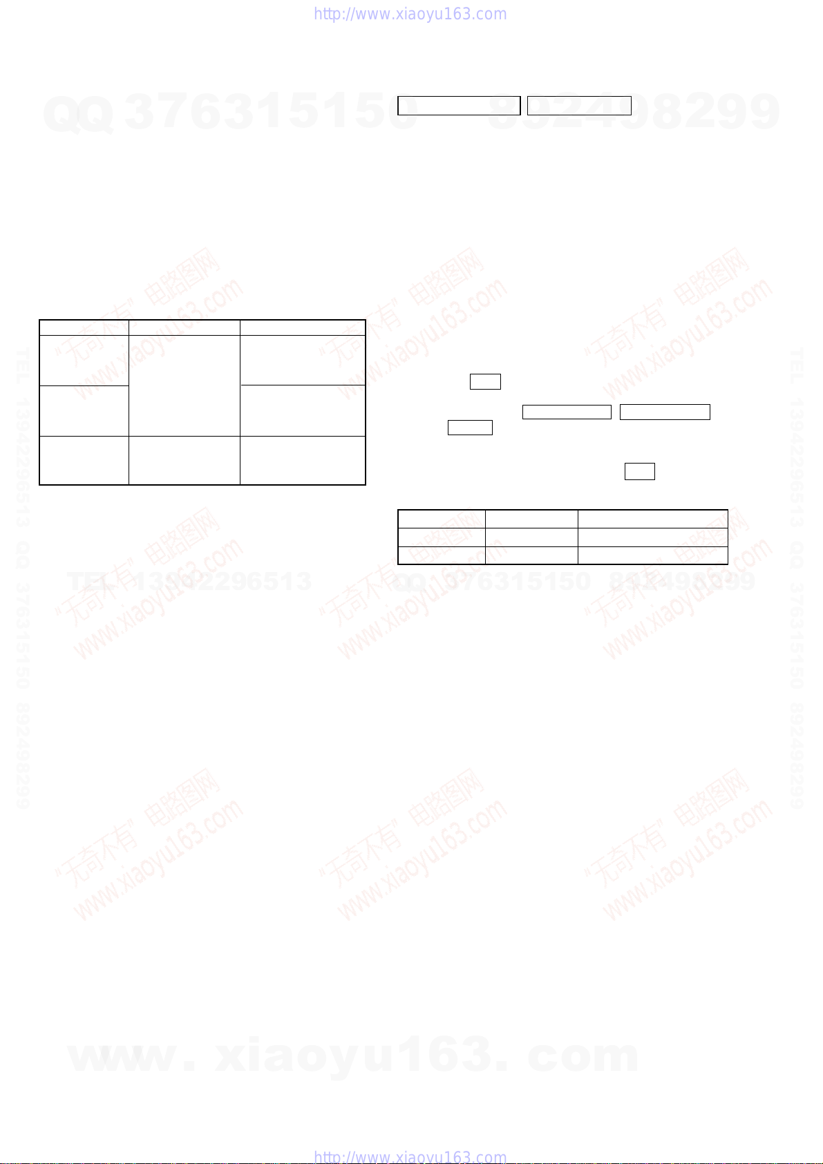
Torque Measurement
Mode Torque Meter Meter Reading
TEL 13942296513 QQ 376315150 892498299
FWD (30 to 70 g•cm)
FWD
back tension (2 to 6 g•cm)
FF/REW CQ-201B (80 to 170 g•cm)
3
7
6
CQ-102C
1
3
2.9~6.9 mN•m
5
(0.42 – 0.97 oz•inch)
0.19~0.59 mN•m
(0.03 – 0.08 oz•inch)
7.8~16.7 mN•m
(1.11 – 2.36 oz • inch)
1
5
0
ELECTRICAL ADJUSTMENTS
DECK SECTION 0 DB = 0.775 V
Precaution
1. Demagnetize the record/playback head with a head demagnetizer.
2. Do not use a magnetized screwdriver for the adjustments.
3. After the adjustments, apply suitable locking compound to the
parts adjust.
4. The adjustments should be performed with the rated power
supply voltage unless otherwise noted.
5. The adjustments should be performed in the order given in
this service manual. (As a general rule, playback circuit
adjustment should be completed before performing recording
circuit adjustment.)
6. The adjustments should be performed for both L-CH and R-CH.
7. Switches and controls should be set as follows unless other-wise
specified.
8. Set to the DOLBY NR OFF.
9. Set to the test mode.
(1) Press the \/1 button to turn the power ON.
(2) Select the function “TAPE A or B”.
(3) Press the button of c/CLOCK SET , TUNER ENTER ,
and DISC 3 simultaneously, to set the tape deck test mode
and displays “TEST MODE” on the fluorescent indicator
tube.
(4) To release from the test mode, press the \/1 button.
SECTION 6
9
8
2
4
9
8
2
9
9
TEL 13942296513 QQ 376315150 892498299
TEL
13942296513
• T est Tape
Tape Signal Used for
P-4-A100 10 kHz, – 10 dB Azimuth Adjustment
WS-48B 3 kHz, 0 dB Tape Speed Adjustment
9
8
0
5
1
5
1
3
6
7
3
Q
Q
2
4
9
8
2
9
9
18
w
w
w
.
xia
o
y
u
1
6
3
.
c
o
m
)
HCD-XGV6/XGV8/XGV10AV
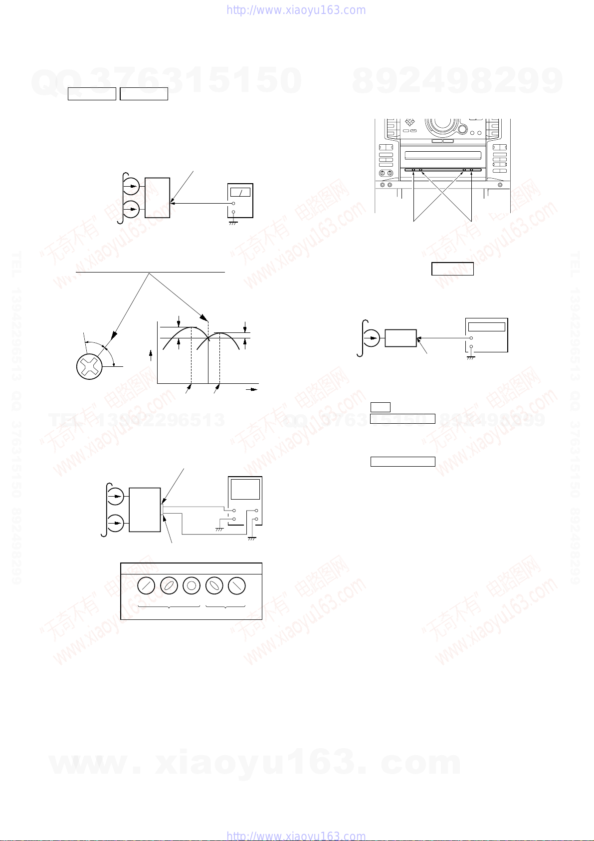
Record/Playback Head Azimuth Adjustment
Q
Q
DECK A DECK B
Note: Perform this adjustments for both decks
Procedure:
1. Mode: Playback (FWD)
TEL 13942296513 QQ 376315150 892498299
2. Turn the adjustment screw and check output peaks. If the peaks
do not match for L-CH and R-CH, turn the adjustment screw
so that outputs match within 1dB of peak.
L-CH
peak
Screw
position
TEL
3. Mode: Playback
7
3
test tape
P-4-A100
(10 kHz, – 10 dB)
R-CH
peak
6
Output
level
set
1
3
MAIN board
MD (VIDEO) OUT jack (J701
L-CH, R-CH
within
1dB
L-CH
peak
13942296513
MAIN board
test tape
P-4-A100
(10 kHz, – 10 dB)
L-CH
set
R-CH
MD (VIDEO) OUT jack (J701)
L-CH
R-CH
5
R-CH
peak
1
5
level meter
+
within
1dB
oscilloscope
H
V
0
Screw
position
Q
Q
Adjustment Location: Playback Head (Deck A).
B).
Tape Speed Adjustment DECK B
Mode: Playback
test tape
WS-48B
(3 kHz, 0 dB)
1. Insert the WS-48B into the deck B.
2. Press the H button on the deck B.
3. Press the H SPEED DUB button in playback mode.
7
3
Then at HIGH speed mode.
4. Adjust RV392 on the LEAF SW board do that frequency
counter reads 6,000 ± 180 Hz.
5. Press the H SPEED DUB button.
Then back to NORMAL speed mode.
6. Adjust RV391 on the LEAF SW board so that frequency
counter reads 3,000 ± 90 Hz.
Adjustment Location: MAIN board
Sample value of Wow and Flutter: 0.3% or less W.RMS (JIS)
8
6
3
9
1
5
4
2
forward
set
1
5
Record/Playback/Erase Head (Deck
MAIN board
MD (VIDEO) OUT jack (J701)
L-CH, R-CH
8
0
8
9
reverse
frequency counter
2
9
2
9
+
–
2
8
9
4
(WS-48B)
9
9
TEL 13942296513 QQ 376315150 892498299
9
waveform of oscilloscope
in phase 45°90°135°180
good
4. Repeat step 1 to 3 in playback (REV) mode.
5. After the adjustments, apply suitable locking compound to the
pats adjusted.
w
w
w
.
xia
o
°
wrong
y
u
1
6
3
.
c
o
m
19
HCD-XGV6/XGV8/XGV10AV
e
r
r
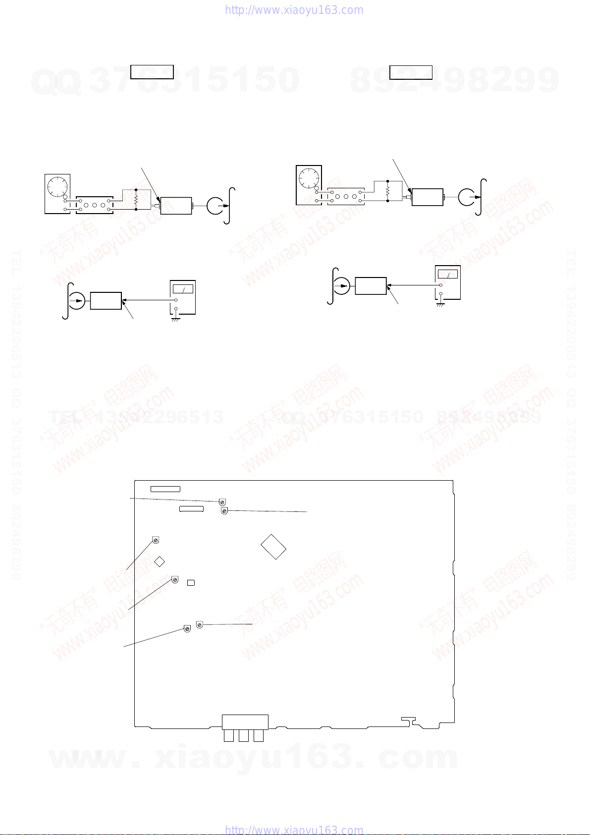
REC Bias Adjustment DECK B
Procedure:
Q
Q
1. Mode: Record
FUNCTION: VIDEO
AF OSC
attenuator
2. Mode: Playback
TEL 13942296513 QQ 376315150 892498299
recorded
portion
3. Confirm playback the signal recorded in step 1 become specification values as follows.
If these values are out of specification values, adjust the RV321
(L-CH) and RV322 (R-CH) on the MAIN board to repeat
steps 1and 2.
TEL
Adjustment level: The playback output of 10kHz level difference
Adjustment Location: MAIN board
– MAIN BOARD (Component Side) –
7
3
MAIN board
MD(VIDEO) IN jack (J701)
L-CH, R-CH
1) 315 Hz
2) 10 kHz
set
6
50 mV (– 23.8 dB)
600
Ω
MAIN board
CN301 pin
pin
3
set
level mete
1
(L-CH)
3
(R-CH)
1
+
–
5
blank tap
CS-123
13942296513
against 315 Hz reference should ±0.5 dB.
1
5
REC Level Adjustment DECK B
Procedure:
0
1. Mode: Record
FUNCTION: VIDEO
AF OSC
attenuator
2. Mode: Playback
recorded
portion
3. Confirm playback the signal recorded in step 1 become specification values as follows.
If these values are out of specification values, adjust the RV351
(L-CH) and RV301 (R-CH) on the MAIN board to repeat steps
1 and 2.
Specification values:
Q
Q
CN301 playback level: 47.2 to 53.0 mV (– 24.3 to – 23.3 dB)
3
7
4
2
9
8
MAIN board
MD (VIDEO) IN jack (J701)
L-CH, R-CH
315 Hz, 50 mV (– 23.8 dB)
600
Ω
set
level mete
set
6
3
MAIN board
CN301 pin
pin
5
1
1
5
0
1
(L-CH)
3
(R-CH)
9
+
–
8
9
8
blank tape
CS-123
4
2
2
9
8
9
2
9
9
TEL 13942296513 QQ 376315150 892498299
9
w
w
RV392
TAPE SPEED
(HIGH)
RV301
REC LEVEL
(R-CH)
RV351
REC LEVEL
(L-CH)
RV321
REC BIAS
(L-CH)
w
1
.
xia
CN371
IC301
19
1
CN431
1
CN301
RV391
IC501
1
TAPE SPEED
(NORMAL)
6
3
.
c
o
m
15
3
RV322
REC BIAS
(R-CH)
IN
OUT
MD (VIDEO)
o
y
u
20
e
B=1.3 ± 0.6Vp-p
symmetry
A (DC voltage)
center of
waveform
B
0V
Specified level: × 100=less than – 22%
B
A
DVC
RFDC
RFAC
TE
FE
SE
DVC
HCD-XGV6/XGV8/XGV10AV
CD SECTION
7
Q
Q
TEL 13942296513 QQ 376315150 892498299
3
Note :
1. CD Block is basically designed to operate without adjustment.
Therefore, check each item in order given.
2. Use LUV-P01 (4-999-032-01) unless otherwise indicated.
3. Use an oscilloscope with more than 10M impedance.
4. Clean the object lens by an applicator with neutral detergent
when the signal level is low than specified value with the
following checks.
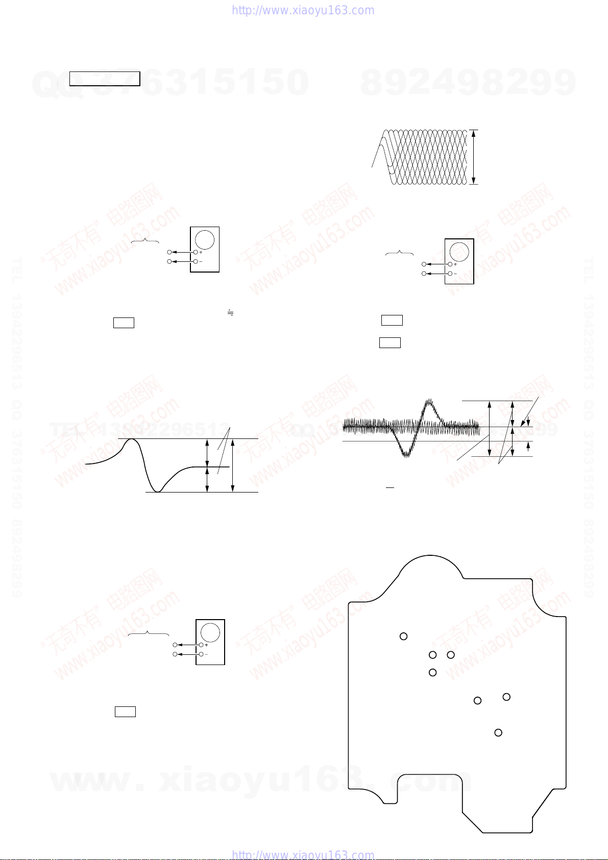
S-Curve Check
Procedure :
1. Connect oscilloscope to TP (FE).
2. Connect between TP (FE) and TP (DVC ( 1.65 V)) by lead wire.
3. Press the \/1 button to turn the power ON.
4. Load a disc (LUV-P01) and actuate the focus search. (In consequence of open and close the disc tray, actuate the focus search)
5. Confirm that the oscilloscope waveform (S-curve) is symmetrical between A and B. And confirm peak to peak level within 2
±0.5 Vp-p.
6
BD board
TP(FE)
TP(DVC)
1
3
Oscilloscope
5
1
5
0
Note: Clear RF signal waveform means that the shape “◊” can be
clearly distinguished at the center of the waveform.
E-F Balance (1 Track jump) Check
Procedure:
1. Connect oscilloscope to TP (TE) and TP (DVC) board.
2. Press the \/1 button to turn the power ON.
3. Load a disc (LUV-P01) and playback the number nine track.
4. Press the bB button. (Becomes the 1track jump mode.)
5. Confirm that the level B and A (DC voltage) on the oscilloscope
waveform.
8
2
9
BD board
TP(TE)
TP(DVC)
4
9
VOLT/DIV : 200mV
TIME/DIV : 500ns
oscilloscop
2
8
level : 1.45
9
±
0.3Vp-p
9
TEL 13942296513 QQ 376315150 892498299
S-curve waveform
symmetry
TEL
w
13942296513
A
within 4
B
6. After check, remove the lead wire connected in step 2.
Note : • Try to measure several times to make sure than the ratio
of A : B or B : A is more than 10 : 7.
• Take sweep time as long as possible and light up the
brightness to obtain best waveform.
RF Level Check
oscilloscope
BD board
TP(RFDC)
TP(RFAC)
Procedure :
1. Connect oscilloscope to TP (RFDC) and TP (RFAC).
2. Press the \/1 button to turn the power ON.
3. Load a disc (LUV-P01) and playback.
4. Confirm that oscilloscope waveform is clear and check RF
signal level is correct or not.
w
w
.
xia
o
y
±
1Vp-p
u
Q
Q
1
3
6
7
3
Checking Location:
[BD BOARD]
6
3
.
1
1
5
c
0
5
o
9
8
m
2
4
9
8
2
9
9
21
HCD-XGV6/XGV8/XGV10AV
e
VIDEO SECTION
Q
Q
Note :
1. VIDEO board is basically designed to operate without adjustment. Therefore, check each item in order given.
2. Use HLX-504 (J-6090-088-A) or HLX-505 (J-6090-089-A)
unless otherwise indicated.
3. Use an oscilloscope with more than 10MΩ impedance.
4. Clean the object lens by an applicator with neutral detergent
when the signal level is low than specified value with the
following checks.
Video Level Adjustment (VIDEO BOARD)
Purpose
This adjustment is made to satisfy the NTSC standard, and if not
adjusted correctly, the brightness will be too large or small.
TEL 13942296513 QQ 376315150 892498299
set
Procedure:
1. Connect oscilloscope to VIDEO output.
2. Load a disc (HLX-504 or HLX-505) playback.
3. Adjust the RV501 to attain 1.0±0.1Vp-p.
7
3
J721
VIDEO OUTPUT
6
75
Ω
3
Oscilloscop
1
5
1
5
VIDEO BOARD (SIDE A)
0
CN101
8
9
IC505
2
IC508
4
CN301
8
9
RV501
VIDEO LEVEL
2
9
9
TEL 13942296513 QQ 376315150 892498299
TEL
(WHITE 100%)
13942296513
1.0 ± 0.1 Vp-p
Q
Q
3
7
6
3
1
5
1
5
0
8
9
2
4
9
8
2
9
9
22
w
w
w
.
xia
o
y
u
1
6
3
.
c
o
m
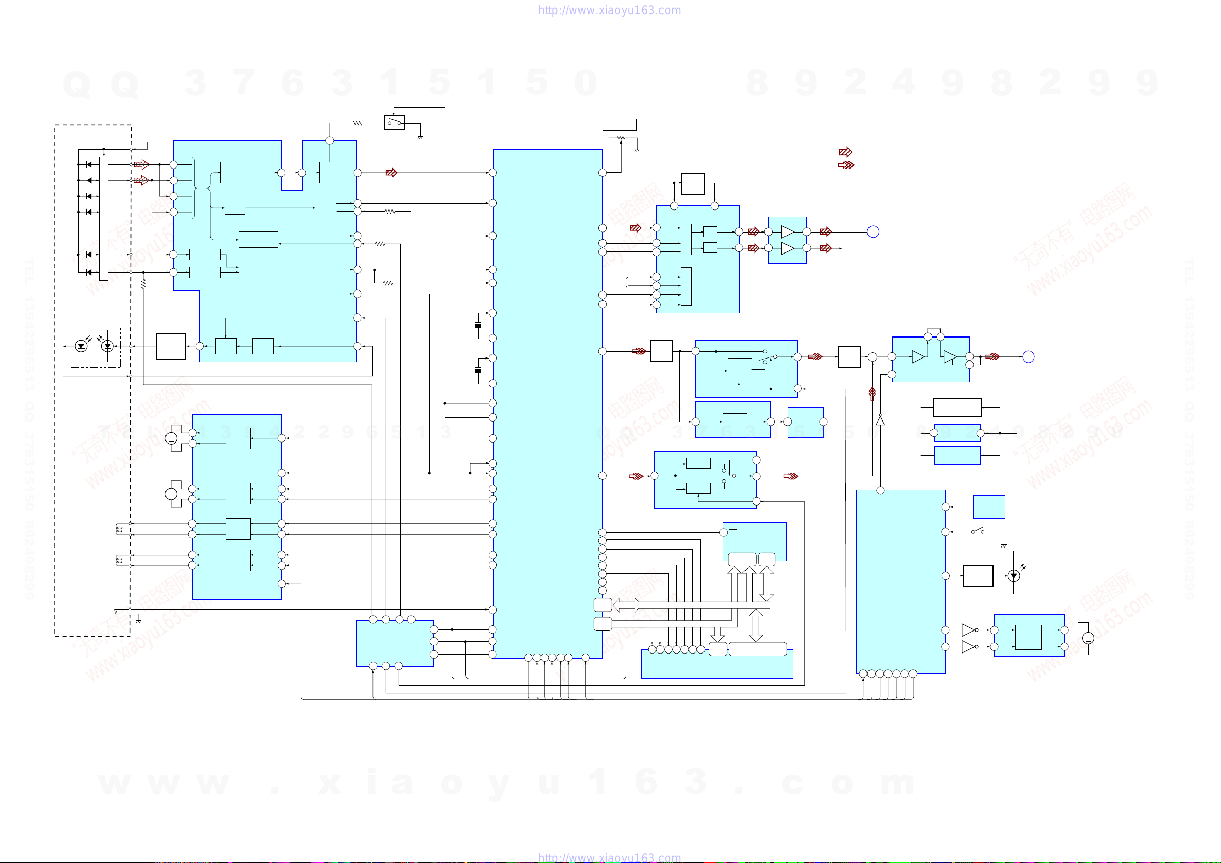
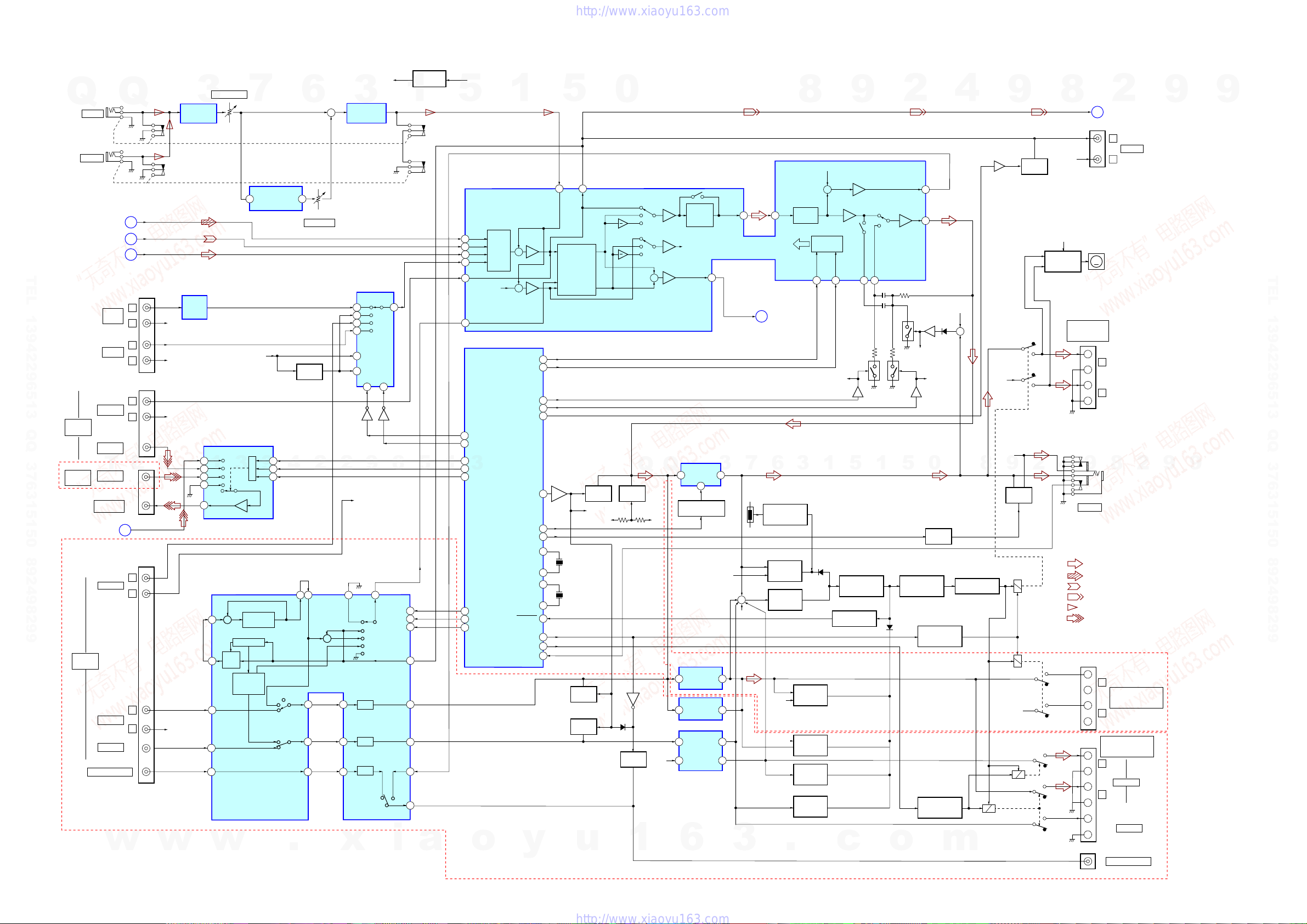
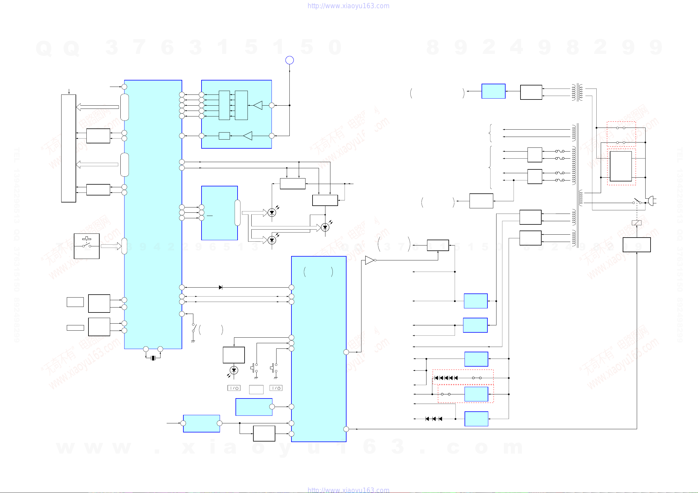
SECTION 7
DIAGRAMS
7-1. CIRCUIT BOARD LOCATION
Q
TEL 13942296513 QQ 376315150 892498299
T
Q
E
L
3
PANEL VR board
MIC/GUITAR board
1
7
TC-A board
CD-L board
3
6
PANEL FL board
9
4
CD-R board
2
3
TRANS board
2
9
1
SUB TRANS board
HEADPHONE board
6
5
FRONT INPUT board
1
5
1
TUNER PACK
(FM/AM TUNER UNIT)
TC-B board
3
5
MAIN board
SUB AMP board
(XGV8/XGV10)
PROLOGIC board
(XGV10)
PA board
VIDEO board
0
Q
Q
1
2
5
8
Note on Schematic Diagram:
• All capacitors are in µF unless otherwise noted. pF: µµF
50 WV or less are not indicated except for electrolytics
and tantalums.
• All resistors are in Ω and 1/
specified.
2
•
• 5 : fusible resistor.
• C : panel designation.
• A : B+ Line.
• B : B– Line.
• H : adjustment for repair.
• Voltages and waveforms are dc with respect to ground
• Voltages are taken with a VOM (Input impedance 10 MΩ).
• Waveforms are taken with a oscilloscope.
• Circled numbers refer to waveforms.
• Signal path.
• Abbreviation
: nonflammable resistor.
Note:
The components identified by mark 0 or dotted line
with mark 0 are critical for safety.
Replace only with part number specified.
under no-signal conditions.
BD board section
no mark: CD PLAY
Other board section
no mark: TUNER (FM/AM)
( ): TAPE PLAY
< >: TAPE REC
[ ]: CD PLAY
Voltage variations may be noted due to normal production tolerances.
Voltage variations may be noted due to normal production tolerances.
3
6
7
3
F : TUNER (FM/AM)
E : TAPE PALY (DECK A)
d : TAPE PALY (DECK B)
G : RECORD
J : CD PALY (ANALOG OUT)
N : MIC INPUT
g : VIDEO
SP : Singapore model
TH : Thai model
EA : Saudi Arabia model
9
4
W or less unless otherwise
5
1
0
HCD-XGV6/XGV8/XGV10AV
9
2
8
4
9
Note on Printed Wiring Boards:
• X : parts extracted from the component side.
• : Pattern from the side which enables seeing.
(The other layers´ Patterns are not indicated.)
• Indication of transistor.
C
Q
B
E
Q
B
CE
Q
B
CE
• Abbreviation
SP : Singapore model
TH : Thai model
EA : Saudi Arabia model
9
8
8
These are omitted.
These are omitted.
These are omitted.
4
2
2
9
9
9
TEL 13942296513 QQ 376315150 892498299
9
w
w
SENSOR board
D-SW board
MOTOR board
w
.
x
i
LED board
a
o
BD board
y
u
1
6
2323
3
.
c
o
m
HCD-XGV6/XGV8/XGV10AV
7-2. BLOCK DIAGRAMS
– CD SERVO SECTION –
7
RF AMP,
IC103
RF
SUMMING
AMP
∑
A-D
FOCUS
ERROR AMP
TRACKING
ERROR AMP
LD
APC LD
AMP
FOCUS/TRACKING COIL DRIVE,
SPINDLE/SLED MOTOR DRIVE
3
-
-
-
-
IC102
MOTOR
DRIVE
MOTOR
DRIVE
COIL
DRIVE
COIL
DRIVE
9
APC PD
AMP
VREF
IN3+
IN3
IN2+
IN2
IN1+
IN1
STBY
IN4
4
-
-
-
6
4 3
23
22
27
26
32
31
35
34
8
EQ_IN
VDC
BUFFER
2
DATA DECODERR,
D/A CONVERTOR
RST
26
RFC
RF EQ
AMP
DC
AMP
2
IC506
3
RFACAC_SUM
RFDCO
RFDCI
FE
FEI
TE
VDC
SW
PD
9
15
28
29
16
17
18
14
12
2
11
10
LD
DRIVE
Q101
M
M
3
FOCUS/TRACKING ERROR AMP
A
6
B
7
C
8
D
9
F
F I-V AMP
E
E I-V AMP
1
VO4+
5
1
VO4
10
VO3+
1
VO3
2
VO2
56
VO2+
55
VO1
52
VO1+
47
Q
TEL 13942296513 QQ 376315150 892498299
OPTICAL PICK-UP BLOCK
(A-MAX.3)
ON: when the optical pick-up
(
is inner position.
A
B
C
D
F
E
LASER DIODE
PD
T
TRACKING
COIL
FOCUS
COIL
S101
(LIMIT)
Q
PD1
PD2
I-V AMP
I1-6
I5-10
LD
LD
PD
E
T+
F+
CD D+5V
M101
L
SPINDLE
MOTOR
M102
SLED
MOTOR
T-
F-
(
1
Q102
TE
6
5 9 3
AO4
RST
4 13 2
RST
LD-ONFERFDC
5
6
AO6
AO3
AO5
AO2
AO1
HUE
SHARPNESS
1
CLK
5
DI
LD
12
11
10
X502
27MHz
X501
33.8688MHz
3
DATA
CLK
1
173
160
164
162
163
206
207
149
150
24
189
133
161
165
137
138
140
141
142
143
135
30
29
28
RFAC
RFDC
FE
TE
SE
CLKA
CLKB
XTAI
XTAO
GPIO9
XTSL
MDP
CE
VC
SFDR
SRDR
TFDR
TRDR
FFDR
FRDR
SSTP
GPIO14
GPIO13
GPIO12
5
CD-DSP,
DIGITAL SERVO,
MPEG DECODER, DAC
IC505
GPIO0
GPIO1
GPIO2
GPIO3
13 14 15 16 18 19
SI
SO
SCK
SOK
SRQ
GPIO4
SCS
0
AUDDTO0
AUDLRCK
AUDBCK
GPIO11
AUDLRCK
CPSIG
NVOEL
DRDQM1
DRDQM0
DRCK
DRBS
DRRAS
DRCAS
DRWEL
DRDAT0
I
DRDAT15
DRADR0
I
DRADR10
SYS RST
GPIO5
81
RST
VRF
CSIA
VIDEO LEVEL
+2.5V
3
201
204
203
26
205
6
Q
7
74
78
77
70
76
72
68
73
49-56,
59-66
34-37,
39-45
RV501
Y
C
Q
DATA
CLK
LAT
MCLK
A+5V
(5W)
16
6 5
VCC
DATA
2
I/F
LRCK
3
BLK
1
13
14
15
16
BAFFER
Q301
SYNC
DETECT
IC301
3
VIN
1
HUE CONTROL
17 18 20 38 15 39
WE
BA0
CAS
RAS
5
3
1
LPF
IC102
V_OUT
CONT
9
1
5
DELAY
IC302
5
8
+3.3V
REG
Q581
DAC
DAC
CONTROL
V_IN THRU
10
VIDEO
6 3 1 10
7
BURST
COLOR
IC303
CLK
LDQM
UDQM
D/A
CONVERTOR
IC504
VDD
LOUT CD-L
7
ROUT
8
SHARPNESS
CONTROL
IC304
DIFF
CONTROL
PC
AMP
SYNC
IN
34-37,
29-34
A0-A9
6
24
OUT
SYNC
SEPA
3
BGP
5
VOUT
6
TINT
8
ROM
DE
IC508
A0-A16 DQ0-DQ7
2-12,23,
13-15,
25-31
7-21
0-7
8-15
0-15
2,4,5,7,8,10,11,13,
42,44,45,47,48,50,51,53
DQ0-DQ15
SDRAM
IC507
D+5V
9
(SW)
IC201
G
D201
(DISC No.)
MOTOR
DRIVE
2
(Page 26)
8
OUT2
OUT1
2
3
7
9
9
M
(TABLE)
9
TEL 13942296513 QQ 376315150 892498299
9
M201
2
• R-ch is omitted due to same as L-ch.
• Signal Path
: CD PLAY (ANALOG)
: VIDEO
7
1
1
R-CM
BUFFER
Q302
5
35
4
(Page 26)
A
VIDEO AMP
IC307
Y/C MIX
0
(CD MECHANISM CONTROL)
CD-DATA
SI
BUF
IN
8
+
2
STB
+4.5V
(IC103)
Q370
+2.5V
+3.3V
V-MUTE
33
SQ-CLK
BU UP/DW SW
SYSTEM CONTROLLER
IC501 (1/4)
SQ-DATA
XLT
CD-CLK
SCOR
HOLD
4036 37 193243
SO
SCS
SCK
SOK
SRQ
MTR-CTRL1
RST
8
TBL-SENS
LED-DISK
MTR-CTR2
XRST
9
31
RIPPLE FILTER
+2.5V REG
3
9
IC201
+3.3V REG
IC202
49
48
47
44
45
OUT
Q201
6
5
1
2
DISC TABLE
SENSOR
IC202
S201
(UP SWITCH)
LED DRIVE
Q201
Q412
Q411
8
VCD-VIDEO
4
TABLE MOTOR DRIVER
IN2
1
IN1
9
w
w
w
.
x
i
a
o
y
u
1
6
2424
3
.
c
o
m
–TUNER/TAPE DECK SECTION –
HCD-XGV6/XGV8/XGV10AV
7
RV321
REC
BIAS(L)
T331
3
9
FM/AM TUNER UNIT
ST-LOUT
FM ANT
FM ANT
AM ANT
AM ANT
ST-ROUT
ST-MUTE
OUT(ST-DIN)
IN(ST-DOUT)
6
C322,L321
BIAS
TRAP
4
STEREO
TUNED
ST-CLK
ST-CE
.
2
1
2
3
BIAS OSC
Q331,332
RIPPLE
FILTER
Q333
2
R-CH
ST-MUTE
STEREO
TUNED
ST-DIN
ST-DOUT
ST-CLK
ST-CE
x
3
REC/PB SWITCH
IC321
9
ST-L
D
ANTENNA
3
R-CH
R-CH
R-CH
1
w
Q
TEL 13942296513 QQ 376315150 892498299
Q
PB
HEAD
REC/PB
HEAD
ERASE
HEAD
T
E
FM
75Ω
AM
w
DECK-A
DECK-B
L
TC BLOCK
REC(REW)
REC(FWD)
B-PHOTO
A-PHOTO
B-MODE
A-MODE
B-HALF
A-HALF
A-SOL
B-SOL
CAP M+
MOTOR-L
MOTOR-H
CN371
w
1
R-CH
TC A+10
6
(Page 26)
i
4
Q334,335
5
a
5
SWITCH
Q321,322
1
Q383,384
A TRIG
DRIVE
Q381,382
B TRIG
DRIVE
Q385,386
CAP MOTOR
DRIVE
Q387,388
CAP MOTOR
SPEED CONT
RV391
RV392
3
o
1
32
34
21
RV931
TAPE SPEED
LOW
RV932
TAPE SPEED
HIGH
y
A
B
REC-OUT
5
u
0
R-CH
70
120
DECK A/B SELECT
PB/REC EQUALIZER AMP
IC301
Q
Q
1
IC341
NORM/HIGH
ALC ON/OFF
3
3
HPF
MUTE
Q344,345
REC MUTE ON/OFF
7
+
28 27 26
A/B
13 12 11 15 14
6
AMS DETECT
PB-OUT1
ALC1
MUTE ON/OFF
6
.
8
Q341-343
3
9
2
4
PB-L
B
9
(Page 26)
8
2
9
9
TEL 13942296513 QQ 376315150 892498299
RV351
REC(L)
LEVEL
23
(CD MECHANISM CONTROL)
53
AMS-IN
58
TC-MUTE
61
REC-MUTE
68
ALC
66
EQ-H/N
5
1
5
1
c
67
PB-A/B
BIAS
65
REC-B
50
REC-A
46
90
B-SHUT
A-SHUT
89
57
B-PLAY SW
56
A-PLAY SW
B-HALF
91
A-HALF
70
69
TC-RELAY
51
A-TRIG
52
B-TRIG
CAPM-CTRL
55
CAPM-H/L
54
ST-MUTE
21
STEREO
2
TUNED
3
ST-DIN
25
ST-DOUT
23
27
ST-CLK
ST-CE
22
o
REC-L
SYSTEM CONTROL
IC501(2/4)
0
m
8
C
(Page 26)
9
2
8
9
4
2
• R-ch is omitted due to same as L-ch.
• SIGNAL PATH
: TUNER (FM/AM)
: PLAYBACK (DECK A)
: PLAYBACK (DECK B)
: RECORD
9
9
2525
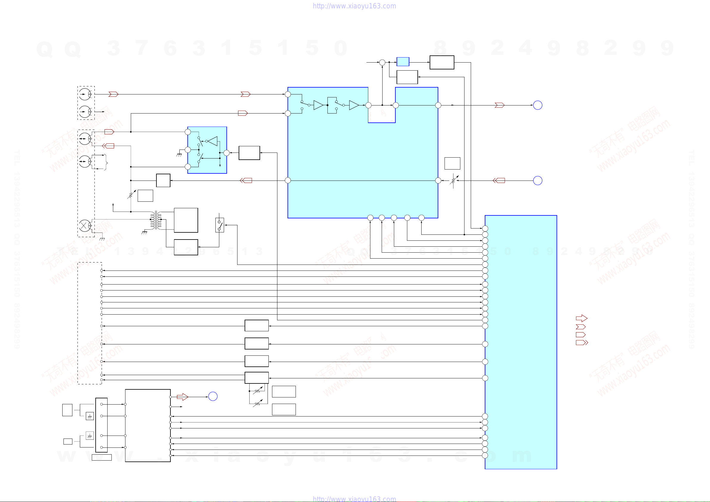
HCD-XGV6/XGV8/XGV10AV
– MAIN SECTION –
VC
RV802
MIC LEVEL
Q
J801
MIC 1
J802
MIC 2
(Page 24)
(Page 25)
(Page 25)
Q
A
B
D
CD-L
PB-L
ST-L
3
GUITAR AMP
IC850(1/2)
7
DIGTAL
LPF1
LPF2
ECHO
1 8
OUT
IN
IC851
6
RV801
ECHO LEVEL
+
IC850 (2/2)
TEL 13942296513 QQ 376315150 892498299
GAME
INPUT
INPUT
XGV10AV
DVD
DVD
INPUT
SUB WOOFER OUT
PHONO
IN
MD IN
AUDIO
VIDEO
T
VIDEO
VIDEO OUT
(Page 24)
FRONT
REAR
CENTER
w
G
J701 (1/2)
L
R
L
R
J804
L
R
J721
E
VCD-VIDEO
J711
L
R
L
R
IC601
R-CH
R-CH
R-CH
L
R-CH
w
PHONO
EQ AMP
VIDEO INPUT
SELECT
IC191
IN4 A
8
IN3
1
6
IN2
4
IN1
1
MUTE
VD-OUT
10
(75Ω)
27
+
(L-R)
26
(L+R)
SL-IN
77
C-IN
76
w
3
6db
VCA
CONTROL
CENTER
MODE
A+10V
B
C
LOGIC
A/D, D/A
LOGIC
9
+5V
REG
Q611
Q181
2
4
2
PRO-LOGIC
SOUND
CONTROL
IC201
2
L-IN
3
5
XGV10AV
4240
+
3
SL
2
1
C
2
1
SRSW-IN
.
SL
1011
C
45
SR
161579
x
(+5V)
3
MIC AMP
FUNCTION SELECT
SWITCH
IC181
X0
X
12
X1
14
X2
15
X3
11
16
VDD
VSS
8
AB
10 9
9
R-CH
172
L
VOL OUT SL
VOL
VOL OUT C
VOL
VR SW IN
VOL
1
VOL OUT SW
13
Q182
6
DATA
LT-IN
i
REQ
SCK
2
1
MIC OUT
5
24
22
23
74
9
3
80
17
a
+5V REG.
Q884
A+10V
5
GRAPHIC EQUALIZER CONTROL,
INC1
5
INB1
4
INA1
3
IND1
6
INEX1
7
SUR1
42
FUNC-SEL0
71
FUNC-SEL1
72
REC/PB/PASS
59
1
3
60
NR-ON/OFF
VIDEO-MUTE
76
SYSTEM CONTROLLER
(CD MECHANISM CONTROL)
77
PL-LAT
78
PL-DAT
PL-CLK
79
o
1
INPUT SELECT SWITCH,
ELECTRICAL VOLUME
IC111
INPUT
+
SELECT
SWITCH
R-CH
+
EQIC-DAT
EQIC-CLK
SW-MODE
DBFB-H/L
AUDIO-OUT
LINE-MUTE
IC501 (3/4)
STK-MUTE
HP-MUTE
XC-OUT
XC-IN
X-OUT
PROTECT
FRONT-RELAY
REAR-RELAY
HP-IN
y
X-IN
80
81
97
94
1
Q802,803
LEVEL SHIFT
82
83
86
11
10
13
15
88
87
85
95
5
2
8
MIC
RECB1
SURROUND OR
DPL BUFFER
X501
32.768KHz
X502
16MHz
MUTE
Q281
MUTE
Q271
u
R-CH
MUTE
Q114
-VEE
0
MUTE
Q115
D811
MUTE
Q731
1
C
A
B
C
A
B
+
Q
TC
+10V
LEVEL
SHIFT
Q804, 807, 808
R-CH
R-CH
XGV6/XGV8
Q
POWER AMP
18 11
STANDBY SWITCH
Q803, 804, 834
XGV8
POWER AMP
14 9
POWER AMP
10 5
IC101(1/2)
14 6
POWER AMP
IC101(2/2)
15 18
6
MID/
BASS &
TREBLE
L+R
IC801
12
IC101
F OUT2
19
3
XGV10AV
R-CH
14 15
SPEANA
7
TH831
+
R-CH
3
COMMAND
(Page 27)
F
6
TEMPERATURE
DETECT SWITCH
Q831, 832
OVER LOAD
DETECT
Q801, 851
DC DETECT
SWITCH
Q433, 434
R-CH
VL
IN1
.
8
VOLUME
CONTROL
3
OVER LOAD
DETECT
Q101, 151
OVER LOAD
DETECT
Q101
OVER LOAD
DETECT
Q181
OVER LOAD
DETECT
Q151
BB-B1
17
1
2
SWOUT
OUT1
5
DETECT SWITCH
D410
o
9
R-CH
+
CPU
INTERFACE
DATA
CLK
BB-A1
22 1621
Q113 Q111
Q169,170 Q167,168
5
1
D401
OVER LOAD
DETECT SWITCH
Q432
PROTECT SWITCH
Q439
c
24
18
Q112
Q165,166
R-CH
OVER LOAD
Q437
RELAY DRIVE
RELAY DRIVE
NC
D803
R-CHR-CH
0
DELAY
Q833
Q401, 402
Q403, 407
m
4
LEVEL SHIFT
R-CH
+
8
PROTECT SWITCH
Q431
RY402
Q805,806
R-CH
9
R-CH
9
Q805,855
RY401
RY402
R-CH
–1
–2
MUTE
RY403
MUTE
Q701
8
REC-L
C
R-CH
J701 (2/2)
FAN MOTOR
B+
M901
(FAN)
M
TM401
FRONT SPEAKER
IMPEDANCE
USE 6 – 16Ω
+
L
–
+
R
–
9
4
J801
PHONES
• R-ch is omitted due to same as L-ch.
• SIGNAL PATH
: TUNER (FM/AM)
: CD PLAY
: TAPE PLAY
: RECORD
: MIC INPUT
: VIDEO
TM402
+
L
–
+
R
2
FAN MOTOR
DRIVE
Q961, 962
–
SURROUND SPEAKER
TM402
+
R
–
+
L
–
+
–
2
(Page 25)
L
MD OUT
R
2
8
SURROUND SPEAKER
IMPEDANCE
USE 8 – 16Ω
IMPEDANCE
USE 8 – 16Ω
REAR
CENTER
J731
SUB WOOFER OUT
XGV8
9
9
9
TEL 13942296513 QQ 376315150 892498299
9
2626
XGV10AV
– DISPLAY/KEY CONTROL/POWER SUPPLY SECTION –
HCD-XGV6/XGV8/XGV10AV
Q
Q
VF
VF(-35V)
GRID DRIVE
Q608, Q609
3
7
FLUORESCENT INDICATOR TUBE DRIVER,
48
1
8
18 – 22,24 – 41
KEY CONTROL
VKK
43,44
SEG-1 – SEG-25
GR-16
GR-9
IC601
6
BPF-F02
BPF-F03
BPF-F04
BPF-F05
BPF-F06
ALL BAND
70
71
72
73
74
75
3
16
15
14
13
12
11
NFF02
INF03
NFF04
INF05
F06
REC
LEVEL
TEL 13942296513 QQ 376315150 892498299
FL601
55
80
78
LED DAT
76
LED SCK
79
2
2
77 41
RESET
60
I2C-DAT
61
I2C-CLK
52
D-SW
DATA
16
17
CLK
18
STB
9
S740
LID (CD)
OPEN/CLOSE
RESET SIGNAL
GENERATOR
IC801
x
FLUORESCENT INDICATOR TUBE
GRID DRIVE
S611,612,S741-751
S601-605,S810-815
S613-618,S801-809
S615,S701-712
S606-610,S752-760
S713-722,S724,S726
T
E
L
KEY
NETWORK
S763
AMS
.>
(JOG DIAL)
S700
VOLUME
w
w
Q606,Q607
ROTARY
ENCODER
S763
ROTARY
ENCODER
S700
16,14 – 12
15
17
1
3
64 – 69
59
58
57
56
w
10,9,7-2
GR9-GR15
GR-2 ,GR-4-GR8
GR-3
GR-1
9
KEY 0 – KEY 5
JOG A
JOG B
VOL A
VOL B
4
XOUT
82 83
X601
4MHz
EVER +3.9V
.
LED SELB
LED SELA
LED LATCH
XIN
1
BAND-PASS FILTER
DET
DET
LED DRIVER
IC701
6
5
D601
31
i
a
5
IC602
B.P.F.
P1 – P21
20-29,1-7,9-12
1
3
LED
DRIVE
Q601
D602 S619
POWER
SAVE
REMOTE CONTROL
RECEIVER
IC603
o
LINE
REC IN
RESET
SWITCH
Q801
IN
1
4
6
S620
ON/OFF
1
(Page 26)
B+ SWITCH
Q901-904
D701-723
D700
y
5
F
SPEANA
SYSTEM CONTROLLER
CD MECHANISM
IC501 (4/4)
OTM-RESET
30
IIC-DATA
29
IIC-CLK
LED-STBY
75
KEY-POWER
74
KEY-ECO
73
SIRCS
4
20
AC-CUT
RESET
12
u
B+ SWITCH
Q602-605
CONTROL
0
D603-613,D805,806
D801-804
CD-POWER
STBY-RELAY
1
Q
38
84
LED
+3.9V
Q
Q922
(CD SENSOR SECTION B+)
(FM/AM TUNER UNIT B+)
(TC MOTOR SECTION B+)
(CD MOTOR SECTION B+)
6
CD A+5V (SW) ,
CD D+5V (SW)
CD MECHANISM
DECK SECTION
7
3
B+
+5V (LED)
(PANEL SECTION B+)
D+5V (UNSW)
(CD TRAY SECTION B+)
D+5V (SW)
D+3.9V
LED
3.9V
–VEE
A+10V
ST +10V
TC+10V
FAN MOTOR B+
TC M+9V
CD M+7V
3
8
EVER +3.9V
SYSTEM CONTROLLER (IC501) ,
FL DRIVER (IC601) B+
VF(–35V)
FL DRIVER (IC601)
B+ SWITCH
Q921
3
6
D911-913
.
9
POWER AMP (IC102,IC801),
PROTECT CIRCUIT
5
1
D961-965
JW962
c
TO FLUORESCENT
INDICATOR TUBE
(FL601)
–35V
REGULATOR
Q903, 908
5
1
+5V
REGULATOR
IC921
+3.9V
REGULATOR
IC922
+10V
REGULATOR
IC931
JW961
+12V
REGULATOR
IC961
XGV6/XGV10AV
+12V
REGULATOR
IC911
o
2
XGV6/XGV8
+5V
REGULATOR
IC901
XGV10AV
4
RECT
D902 – 905
VF
VF
+VL
–VL
+VH
–VH
+10V AC7V
-10V
+15V
0
XGV8
RECT
D832
RECT
D831
RECT
D841 – 844
RECT
D833 – 836
8
m
9
9
F963
F964
F961
F962
2
8
SUB POWER
TRANSFORMER
TRANSFORMER
AC7V
AC12V
AC12V
4
T901
POWER
T951
9
2
8
• Abbreviation
SP : Singapore model
TH : Thai model
EA : Saudi Arabia model
9
XGV10AV : TH,
XGV6 : TH
VOLTAGE
SELECTOR
S901
XGV10AV : EA, SP
XGV8, XGV6 : SP
POWER ON/OFF
RELAY DRIVE
9
2
Q901
9
TEL 13942296513 QQ 376315150 892498299
CN901
AC IN
RY901
9
2727
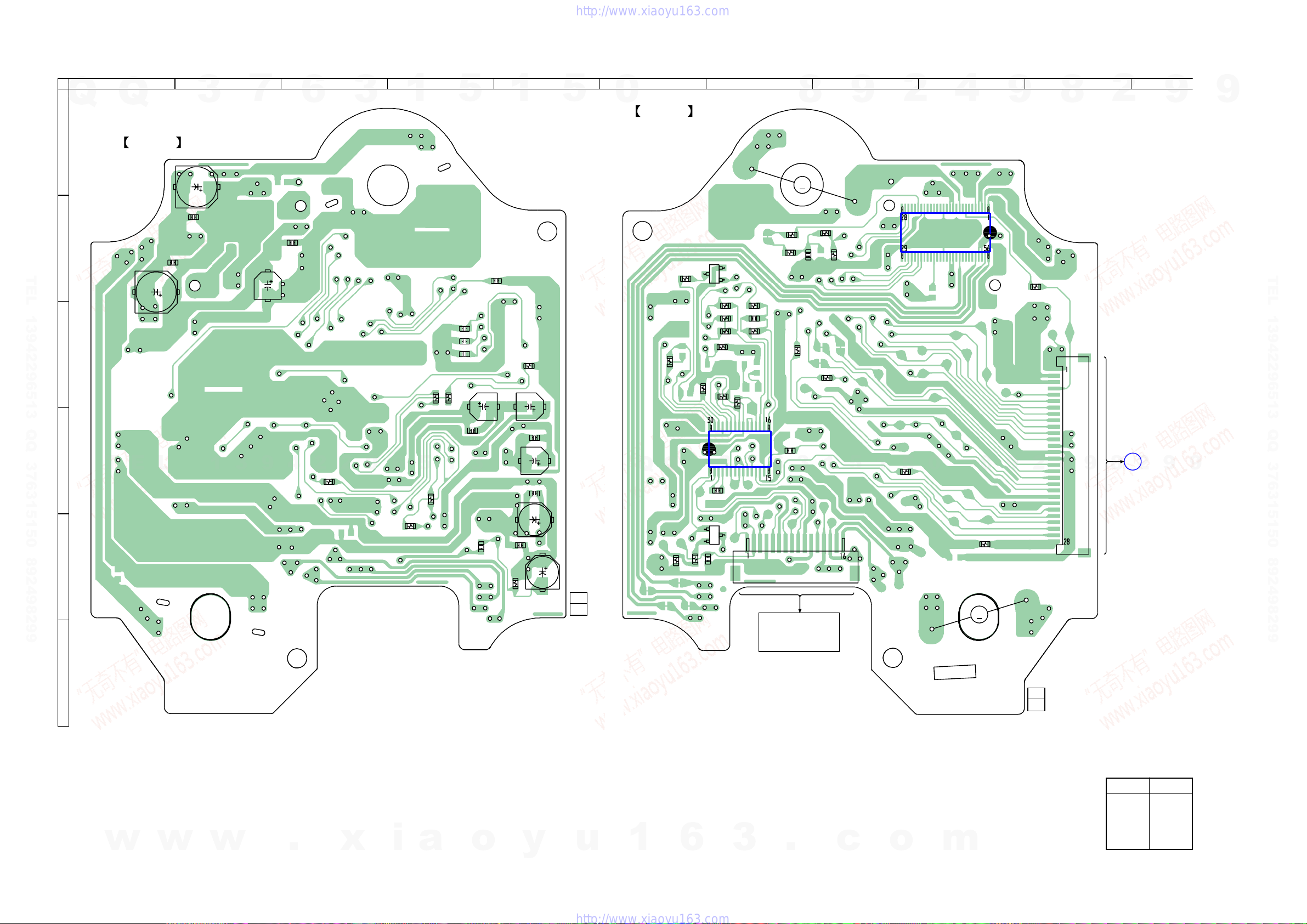
HCD-XGV6/XGV8/XGV10AV
7-3.PRINTED WIRING BO ARD – BD SECTION – • See page 23 for Circuit Boards Location.
3 4 5 6 7
6
2
2
R228
3
9
3
1
2
C163
3
7
C165
9
C153
4
1
Q
A
B
TEL 13942296513 QQ 376315150 892498299
C
D
E
Q
BD BOARD (SIDE A)
C182
T
E
L
C164
C166
6
1
R125
5
R126
C101
R227
1
5
C102
C104
R229
3
C112
C109
C114
C103
C119
C111
C115
1
R117
C120
C108
C117
R122
1-684-174-
C113
5
11
(11)
0
BD BOARD (SIDE B)
R109
R113
Q
Q
R123
R103
R102
R105
E
R124
Q102
R111
R118
R114
3
Q101
C118
E
IC103
C110
–
R179
R176
R104
C107
R120
R112
7
OPTICAL PICK-UP
SPINDLE
MOTOR
6
BLOCK
(A-MAX.3)
8
M101
M
R226
C213
3
R152
C151
R235
CN102
1
R151
8
9
+
5
1
2
R231
5
0
–
IC102
9 10 11
9
2
8
A
VIDEO
BOARD
2
(Page 32)
4
M102
SLED
MOTOR
8
R234
M
9
9
R236
2
+
8
CN101
4
9
9
9
TEL 13942296513 QQ 376315150 892498299
9
F
11
(11)
• Semiconductor
Location
Ref. No. Location
IC102 B-9
IC103 D-7
Q101 E-7
Q102 B-7
w
w
w
.
x
i
a
o
y
u
1
6
2828
3
.
c
o
1-684-174-
m
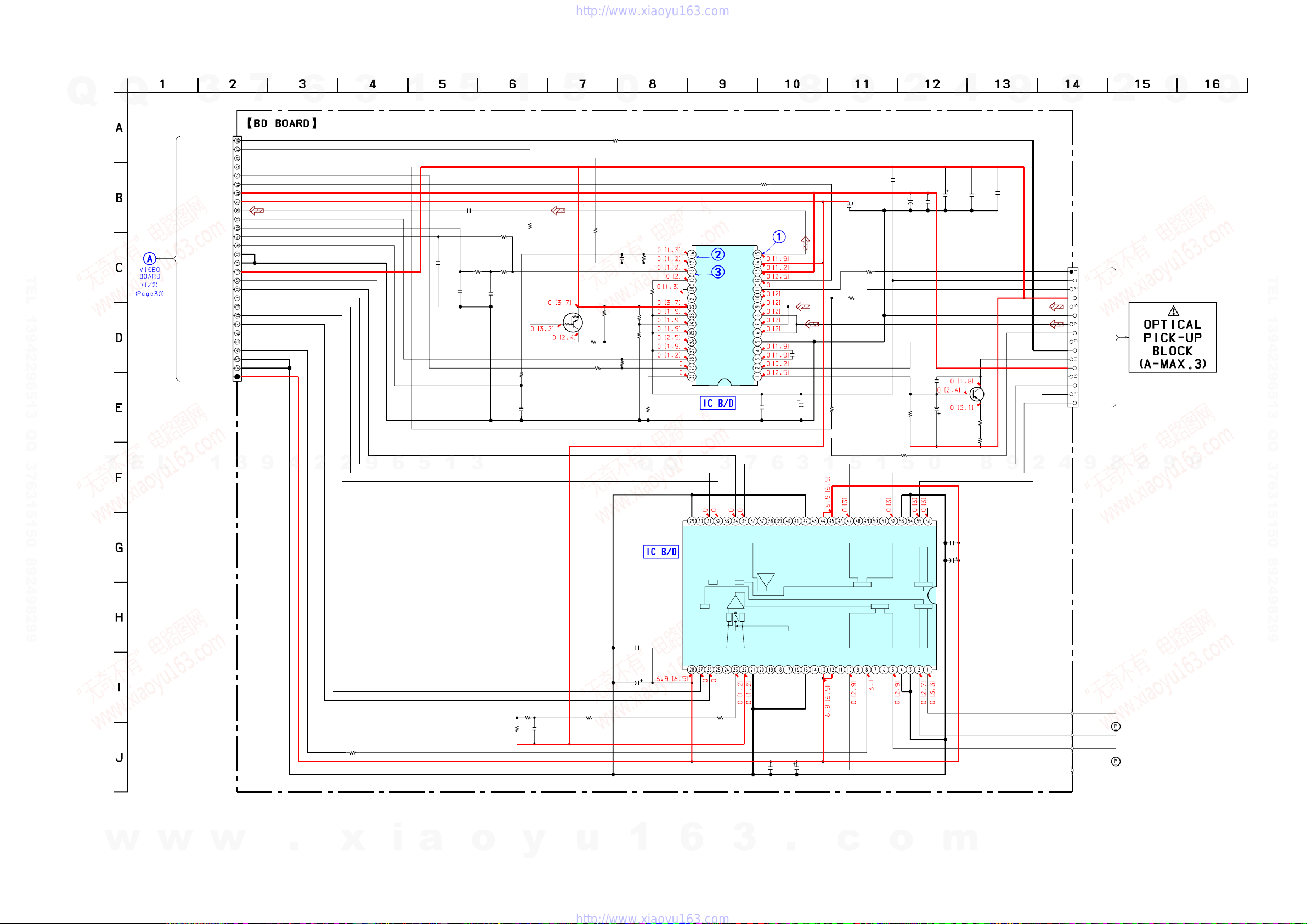
7-4. SCHEMATIC DIAGRAM – BD SECTION –
HCD-XGV6/XGV8/XGV10AV
CN101
28P
DVC
TE
SE
FE
GND
GND
DP
M
GND
GND
7V
7
6
3
Q
Q
TEL 13942296513 QQ 376315150 892498299
3
LD GND
CTRL
D/A1
D/A2
D/A3
LD ON(D/A4)
DVCC(2.5V)
RFAC
RFDC
VCC(4.5V)
SSTP
FRDR
FFDR
TRDR
TFDR
SRDR
SFDR
STBY
M
M
1
C102
0.1
5
C213
0
R102
15k
C101
470p
R103
100k
R105
1k
C104
0.0033
1
R104
C103
15k
470p
R226
1k
UN2111-TX
SW
Q102
5
ITCH
R109
120k
R229
2.2k
R227
100k
R111
120k
0
R234
0
C107
33p
R113
2.7k
R114
47k
R117
47k
R120
120k
R112
CN102
16P
I1-6
VC
I5-10
VCC
PD2
GND
PD1
SW
PD
LD_GND
LD
VCC
TFT+
F+
2
9
9
TEL 13942296513 QQ 376315150 892498299
C118
2
C112
47
1
4V
C114
0.001
C113
100
R122
100k
R235
1k
R228
470k
9
C120
47
4V
R125
33k
R126
33k
8
R231
1k
IC103
CXA2581N-T4
P
RF AM
FE
FEI
TE
TE_BAL
0
R118
0
CE
CEI
VCC
RFG
BST
VFC
RFC
VC
RFDCO
RFDCI
DC_OFST
RFAC
DVC
DVCC
GND
AC_SUM
EQ_IN
SW
PD
LD
F
E
D
C
B
A
C108
0.1
C111
47
4V
C110
0.1
C109
0.1
4V
4
C115
47
6.3V
Q101
2SB710A-RT
LD DRIVE
R124
R123
9
C117
C119
0.1
1
10
10
8
T
E
L
1
3
9
4
2
2
R236
1k
9
6
5
1
3
R151
100k
R152
4.7k
C151
0.022
R176
9
9
2
8
9
4
2
9
C166
0.1
C182
100
10V
8
M
M
102
M
SLED
OTOR
101
M
SPDL
OTOR
0
5
1
5
1
3
6
7
SGND
SVCC
3
IN2-
OPO2(NC)
ABS
IN3+
IN3-
R179
10k
IN2+
OPO1(NC)
-
IN4R
OPO3(NC)
IN1-
+
IN4
IN1+
VREF
OP.O
NC
OP-
-
NC(FB)
C164
OP+
+
NC(SW)
0.1
NC(VDD)
NC(VPUMP1)
NC(CT)
NC(VPUMP2)
C163
100
10V
NC
NC(BC1)
NC(BC3)
NC
PVCC1
NC(BC2)
PVCC2
NC(BC4)
PVCC1
PVCC2
NC
NC
PVCC/2(NC)
STBY
NC
NC
VO1-
VO4+
NC
NC
PGND1
PGND1
PGND2
PGND2
VO2+
VO3-
VO2-
VO3+
NC
VO1+
VO4-
NC
Q
Q
IC102
AN41020A
BTL DRIVE
C153
0.1
C165
10
16V
0
w
w
w
.
x
i
a
o
y
u
1
6
2929
3
.
c
o
m
 Loading...