

Sony HCD-XB66K Schematic

MICROFILM
HCD-XB66K
SERVICE MANUAL
Photo: XB66K
Dolby noise reduction manufactured under license
from Dolby Laboratories Licensing Corporation.
“DOLBY” and the double-D symbol a are trademarks of Dolby Laboratories Licensing Corporation.
CD
Section
Tape deck
Section
E Model
Model Name Using Similar Mechanism HCD290/G330/XB3
CD Mechanism Type CDM37LH-5BD29AL
Base Unit Name BU-5BD29AL
Optical Pick-up Name KSS-213D/Q-NP
Model Name Using Similar Mechanism HCD-H881
T ape Transport Mechanism Type TCM-220WR2
SPECIFICATIONS
Amplifier section
The following measured at AC 120/240 V, 50 Hz
DIN power output (Rated) 140 + 140 watts
(8 ohms at 1 kHz, DIN)
Continuous RMS power output (Reference)
170 + 170 watts
(8 ohms at 1 kHz, 10% THD)
Peak music power output (Reference)
3,000 watts
Inputs
PHONO IN (phono jacks): sensitivity 3 mV, impedance
47 kilohms
MIX MIC (phone jack): sensitivity 1 mV, impedance
10 kilohms
VIDEO/MD (AUDIO) IN (phono jacks):
sensitivity 250 mV, impedance
47 kilohms
Outputs
PHONES (stereo phone jack): accepts headphones of 8 ohms or more
VIDEO/MD (AUDIO) OUT (phono jacks):
voltage 250 mV, impedance 1 kilohms
SPEAKER: accepts impedance of 8 to 16 ohms.
CD player section
System Compact disc and digital audio system
Laser Semiconductor laser (λ = 780 nm)
Emission
duration: continuous
Laser output Max. 44.6 µW*
*This output is the value measured at
a distance of 200 mm from the
objective lens surface on the Optical
Pick-up Block with 7 mm aperture.
Wavelength 780 - 790 nm
Frequency response 2 Hz - 20 kHz (±0.5 dB)
Signal-to-noise ratio More than 90 dB
Dynamic range More than 90 dB
CD DIGITAL OUT
(square optical connector jack, rear panel)
Wave length: 600 nm
Output level: –18 dBm
– Continued on next page –
COMPACT DISC DECK RECEIVER

Tape player section
Recording system 4-track 2-channel stereo
Frequency response (DOLBY NR OFF)
60 - 13,000 Hz (±3 dB),
using a Sony TYPE I cassette
60 - 14,000 Hz (±3 dB),
using a Sony TYPE II cassette
Tuner section
FM stereo, FM/AM superheterodyne tuner
FM tuner section
Tuning range 87.5 - 108.0 MHz (50 kHz step)
Antenna FM wire antenna
Antenna terminals 75 ohm unbalanced
Intermediate frequency 10.7 MHz
AM tuner section
Tuning range
(2 band model) 531 - 1,602 kHz
(with the tuning interval set at 9 kHz)
530 - 1,710 kHz (with the tuning
interval set at 10 kHz)
(3 band model )
MW: 531 -1,602 kHz (with the tuning
interval set at 9 kHz)
LW: 153 - 279 kHz (with the tuning
interval set at 3 kHz)
Antenna AM loop antenna, External antenna
terminals
Intermediate frequency 450 kHz
General
Power requirements
Mexican model: 120 V AC, 50/60 Hz
Australian and South African models:
220 - 240 V AC, 50/60 Hz
Other models: 110 -120 V or 220 -240 V AC,
50/60 Hz Adjustable with voltage
selector
Power consumption 320 watts
Dimensions (w/h/d) Approx. 355 × 425 × 435 mm (14 ×
163/4 × 171/4 in) incl. projecting parts
and controls
Mass Approx. 14.5 kg (31 lb 16 oz.)
Supplied accessories AM loop antenna (1)
Remote RM-SD70S (1)
Size AA (R6) batteries (2)
FM wire antenna (1)
Speaker cords (2)
Design and specifications are subject to change without notice.
TABLE OF CONTENTS
1. SERVICING NOTES............................................... 3
2. GENERAL ................................................................... 4
3. DISASSEMBLY ......................................................... 7
4. TEST MODE.............................................................. 15
5. MECHANICAL ADJUSTMENTS ........................ 17
6. ELECTRICAL ADJUSTMENTS
TAPE DECK Section ...................................................... 17
CD Section ...................................................................... 20
7. DIAGRAMS
7-1. IC Pin Function Description ........................................... 22
7-2. Block Diagram – CD Section – ..................................... 27
7-3. Block Diagram – Tape Deck Section – ......................... 29
7-4. Block Diagram – Main Section (1/2) – ......................... 31
7-5. Block Diagram – Main Section (2/2) – ......................... 33
7-6. Block Diagr am – Display/Key Control/
Power Supply Section – .................................................. 35
7-7. Circuit Boards ................................................................. 37
7-8. Printed Wiring Board – CD Section (1/2) – .................. 39
7-9. Schematic Diagram – CD Section (1/2) – ...................... 41
7-10. Printed Wiring Boards – CD Section (2/2) – ................ 43
7-11. Schematic Diagram – CD Section (2/2) – ...................... 45
7-12. Printed Wiring Boards – Tape Deck Section –.............. 47
7-13. Schematic Diagram – Tape Deck Section – ................... 49
7-14. Printed Wiring Board – Main Section – ........................ 51
7-15. Schematic Diagram – Main Section (1/3) – ................... 53
7-16. Schematic Diagram – Main Section (2/3) – ................... 55
7-17. Schematic Diagram – Main Section (3/3) – ................... 57
7-18. Printed Wiring Board – Power Amp Section – ............. 59
7-19. Schematic Diagram – Power Amp Section – ................. 61
7-20. Printed Wiring Board – Panel Section (1/3) –............... 63
7-21. Schematic Diagram – Panel Section (1/3) –................... 65
7-22. Printed Wiring Boards – Panel Section (2/3) – ............. 67
7-23. Schematic Diagram – Panel Section (2/3) –................... 69
7-24. Printed Wiring Boards – Panel Section (3/3) – ............. 71
7-25. Schematic Diagram – Panel Section (3/3) –................... 73
7-26. Printed Wiring Board – Power Supply Section –........... 75
7-27. Schematic Diagram – Power Supply Section – .............. 76
7-28. Schematic Diagram – Key-Con Section – ...................... 77
7-29. Printed Wiriing Board – Key-Con Section –.................. 77
7-30. Waveforms....................................................................... 79
7-31. IC Block Diagrams ......................................................... 80
8. EXPLODED VIEWS................................................ 83
9. ELECTRICAL PARTS LIST ............................... 92
– 2 –

SECTION 1
SERVICING NOTES
CAUTION
Use of controls or adjustments or performance of procedures
other than those specified herein may result in hazardous radiation exposure.
This appliance is classified as a CLASS 1 LASER product.
The CLASS 1 LASER PRODUCT MARKING is located on
the rear exterior.
Laser component in this product is capable of emitting radiation
exceeding the limit for Class 1.
The following caution label is located inside the unit.
CAUTION : INVISIBLE LASER RADIATION WHEN OPEN AND
INTERLOCKS DEFEATED. AVOID EXPOSURE TO BEAM.
ADVARSEL : USYNLIG LASERSTRÅLING VED ÅBNING NÅR
SIKKERHEDSAFBRYDERE ER UDE AF FUNKTION. UNDGÅ UDSAETTELSE
FOR STRÅLING.
VORSICHT : UNSICHTBARE LASERSTRAHLUNG, WENN
ABDECKUNG GEÖFFNET UND SICHEREITSVERRIEGELUNG
ÜBERBRÜCKT. NICHT DEM STRAHL AUSSETZEN.
VARO!: AVATTAESSA JA SUOJ ALUKITUS OHITETTAESSA OLET ALT-
TIINA NÄKYMÄTTÖMÄLLE LASERSÄTEILYLLE. ÄLÄ KATSO SÄTEESEEN.
VARNING : OSYNLING LASERSTRÅLING NÄR DENNA DEL ÄR ÖPPNAD
OCH SPÄRREN ÄR URKOPPLAD. BETRAKTA EJ STRÅLEN.
ADVERSEL : USYNLIG LASERSTRÅLING NÅR DEKSEL ÅPNES OG
SIKKERHEDSLÅS BRYTES. UNNGÅ EKSPONERING FOR STRÅLEN.
VIGYAZAT!: A BURKOLAT NYITÁSAKOR LÁTHATATLAN LÉZERSU-
GÁRVESZÉLY! KERÜLJE A BESUGÁRZÁST!
NOTES ON HANDLING THE OPTICAL PICK-UP
BLOCK OR BASE UNIT
The laser diode in the optical pick-up block may suffer electrostatic break-down because of the potential difference generated
by the charged electrostatic load, etc. on clothing and the human
body.
During repair, pay attention to electrostatic break-down and also
use the procedure in the printed matter which is included in the
repair parts.
The flexible board is easily damaged and should be handled with
care.
NOTES ON LASER DIODE EMISSION CHECK
The laser beam on this model is concentrated so as to be focused
on the disc reflective surface by the objective lens in the optical
pick-up block. Therefore, when checking the laser diode emission, observe from more than 30 cm away from the objective lens.
LASER DIODE AND FOCUS SEARCH OPERATION
CHECK
Carry out the “S curve check” in “CD section adjustment” and
check that the S curve waveforms is output three times.
Notes on chip component replacement
• Never reuse a disconnected chip component.
• Notice that the minus side of a tantalum capacitor may be damaged by heat.
MODEL IDENTIFICATION
– BACK PANEL –
MODEL PART No.
Singapore, Malaysia model 4-996-413-1π
E, Indonesian model 4-996-413-6π
Saudi Arabia model 4-996-413-7π
Thai model 4-996-413-9π
PART No.
Flexible Circuit Board Repairing
• Keep the temperature of the soldering iron around 270 ˚C during repairing.
• Do not touch the soldering iron on the same conductor of the
circuit board (within 3 times).
• Be careful not to apply force on the conductor when soldering
or unsoldering.
SAFETY-RELATED COMPONENT WARNING!!
COMPONENTS IDENTIFIED BY MARK ! OR DOTTED
LINE WITH MARK ! ON THE SCHEMATIC DIAGRAMS
AND IN THE PARTS LIST ARE CRITICAL TO SAFE
OPERATION. REPLACE THESE COMPONENTS WITH
SONY PARTS WHOSE PART NUMBERS APPEAR AS
SHOWN IN THIS MANU AL OR IN SUPPLEMENTS PUBLISHED BY SONY.
– 3 –
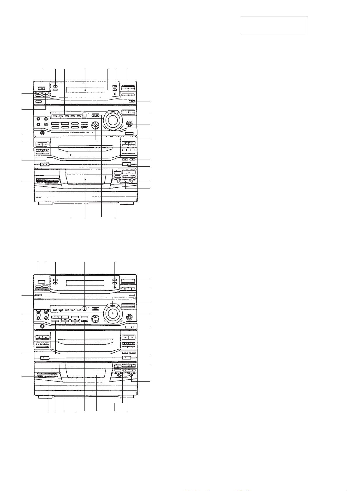
LOCATION OF CONTROLS
– Front Panel –
SECTION 2
GENERAL
This section is extracted
from instruction manual.
!§
!¶
!•
!ª
@º
@¡
1 2 43 5 6 7
@™ @£ @¢ @∞
8
9
0
!¡
!™
!£
!¢
!∞
1 I /u (Power) button
2 DISPLAY/DEMO button
3 FILE (1-5) indicator
4 Fluorescent indicator tube
5 TUNER MEMORY button
6 TUNING MODE button
7 TUNER/BAND button and indicator
8 STEREO/MONO button
9 FUNCTION button
!º SUPER WOOFER button and indicator
!¡ H SPEED DUB button
!™ CD SYNC button
!£ § EJECT button (DECK B)
!¢ ) button (CD)
!∞ ≠ AMS ± jog dial
!§ t/CLOCK SET button
!¶ REC button
!• PHONES jack
!ª GEQ (4/(/$/9) switch
@º § EJECT button (DECK A)
@¡ DIRECT PLAY (DISC 1 to DISC 5) button
@™ Cassette holder
@£ CD lid
@¢ EFFECT button and indicator
@∞ 0 button (CD)
#ª
$º
$¡
$™
$£
@§ @¶ @• @ª #º
$∞$¢ $§ $¶ $• $ª
%º %¡
#¡
#™
#£
#¢
#∞
#§
#¶
#•
@§ DAILY 1 button
@¶ DAILY 2 button
@• SPECTRUM ANAL YZER button
@ª MUSIC/OTHERS/P FILE indicator
#º ENTER/NEXT button and indicator
#¡ TUNING (–) button
#™ TUNING (+) button
#£ GROOVE button and indicator
#¢ VOLUME control knob
#∞ SUPER W MODE button
#§ 6 OPEN button (CD)
#¶ · button and indicator (CD)
#• REPEAT button
#ª SLEEP button
$º MIC1/MIC2 jack
$¡ MIC/ECHO LEVEL control knob
$™ KARAOKE PON/MPX button
$£ NON-STOP button and indicator
$¢ LOOP button
$∞ FLASH button
$§ ENTER button and indicator
$¶ EDIT button
$• 1/ALL DISCS button
$ª PLAY MODE button
%º KEY CONTROL (˜)
%¡ KEY CONTROL (n)
– 4 –

^™
^£
^¢
^∞
^§
%º %¡ %™ %£ %¢ %∞
%º WAVE button
%¡ SURROUND button
%™ P FILE MEMORY button
%£ GEQ CONTROL button
%¢ P button and indicator (DECK B)
%§
%∞ p button (DECK B)
%§ ª button and indicator (DECK B)
%¶ 0 button (DECK B)
%¶
%• · button and indicator (DECK B)
%ª ) button (DECK B)
%•
^º r REC button and indicator (DECK B)
^¡ p button (CD)
^™ · button and indicator (DECK A)
%ª
^£ 0 button (DECK A)
^¢ ª button and indicator (DECK A)
^º
^¡
^∞ p button (DECK A)
^§ DIRECTION button
^¶ DOLBY NR button
^• ) button (DECK A)
^ª DISC SKIP button
&º P button and indicator (CD)
&º^ª^¶ ^•
– Rear Panel –
1 2 3
4
5
6
1 CD DIGITAL OUT OPTICAL
2 FM ANTENN A terminal
3 AM ANTENN A terminal
4 PHONO IN jack
5 VIDEO/MD (AUDIO) IN jack
6 VIDEO/MD (AUDIO) OUT jack
7 SPEAKER output terminal
8 VOLTAGE SELECTOR switch
7 8
– 5 –

– 6 –

DISASSEMBLY
MAIN/KEY-CON BOARD
(Page 8)
CD LID ASS’Y
SECTION
(Page 11)
TAPE MECHANISM
DECK SECTION
(Page 10)
MAIN
SECTION
(Page 9)
AUDIO BOARD
(Page 14)
CASSETTE
LID ASS’Y
(Page 10)
CD MECHANISM
DECK SECTION
(Page 9)
DISC TABLE
(Page 12)
BASE UNIT
(Page 12)
BD BOARD
(Page 13)
PANEL (A)/(B)
SUB ASS’Y
(Page 11)
CAPSTAN MOTOR (M1)
(Page 14)
OPTICAL
PICK-UP
(Page 13)
SLED
MOTOR
(Page 13)
FRONT PANEL
SECTION
(Page 8)
CASE
(Page 7)
• This set can be disassembled in the order shown below.
SECTION 3
Note: Follow the disassembly procedure in the numerical order given.
3-1. CASE
1
Three screws
(case 3 TP2)
3
Case
1
Three screws
(case 3 TP2)
– 7 –
2
Seven screws
(BATT3 × 6)

3-2. FRONT PANEL SECTION
2
Wire (flat type) (11 core)
(CN206)
3
Wire (flat type) (17 core)
(CN102)
5
Front panel section
1
Wire (flat type) (21 core)
(CN205)
4
Four screws
(BVTP3 × 8)
3-3. MAIN/KEY-CON BOARD
2
4
Connector
(CN901)
1
Wire (flat type)
(13 core) (CN201)
Wire (flat type)
(19 core) (CN202)
6
Power cord
7
Back panel
!™
KEY-CON board
(Remove soldering)
!¡
MAIN board
IC201
5
Eleven screws
(BVTP3 × 8)
8
Connector
(CN105)
3
Connector
(CN203)
– 8 –
!º
9
Two screws
(BVTP3 × 8)
Connector
(CN101)
3-4. MAIN SECTION
)
3
Five screws
(BVTP3 × 8)
4
CD mechanism
deck section
(CDM37LH-5BD29AL)
2
Flat wire
and lead wire
1
Open the clamp.
3
2
Connector
(CN203)
Two screws
(BVTP3 × 8)
1
Flat wire (CN202)
4
Main section
3
Screw
(BVTP3
3
Two screws
(BVTP3 × 8
×
8)
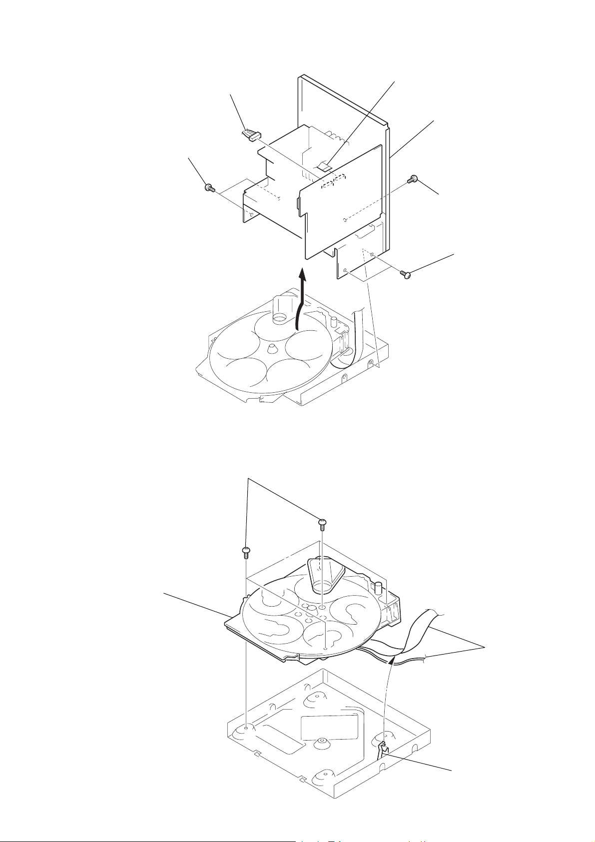
3-5. CD MECHANISM DECK SECTION (CDM37LH-5BD29AL)
– 9 –

3-6. TAPE MECHANISM DECK SECTION (TCM-220WR2)
)
5
Three screws
(BVTP2.6 × 8)
4
Wire (flat type)
(21 core) (CN601)
3
Wire (flat type)
(11 core) (CN1001)
A
5
Three screws
(BVTP2.6 × 8)
6
Remove the tape mechanism deck section
(TCM-220WR2) to direction of the arrow A.
2
Open the
cassette lids.
3-7. CASSETTE LID ASS’Y
1
Two springs
1
Push the
two buttons.
3
Two bracket
2
Two screws
(BVTP2.6 × 8
– 10 –

3-8. CD LID ASS’Y SECTION
)
5
Connector
(CN671)
6
Four screws
(BVTP2.6 × 8)
7
CD lid ass’y
4
Connector
(CN661)
2
Four screws
(BVTP2.6 × 8)
3-9. PANEL (A) / (B) SUB ASS’Y
3
Two claws
1
Connector
(CN642)
3
CD-B1 SW board
1
Connector
(CN612)
2
Four screws
(BVTP2.6 × 8
4
Panel (A) sub assy
5
Two claws
6
Panel (B) sub assy
– 11 –
3-10. BASE UNIT
t
e
3
Base unit
1
Yoke bracke
3-11. DISC TABLE
Note:
When the disc table is installed, adjust the positions
of roller cam and mark ( as shown in the figure,
then set to the groove of disc table.
A
2
Boss
2
Bracket (BU)
1
Screw
(BVTP3 × 8)
1
Screw
(BVTP3 × 8)
3
Step screw
4
Disc tabl
– 12 –
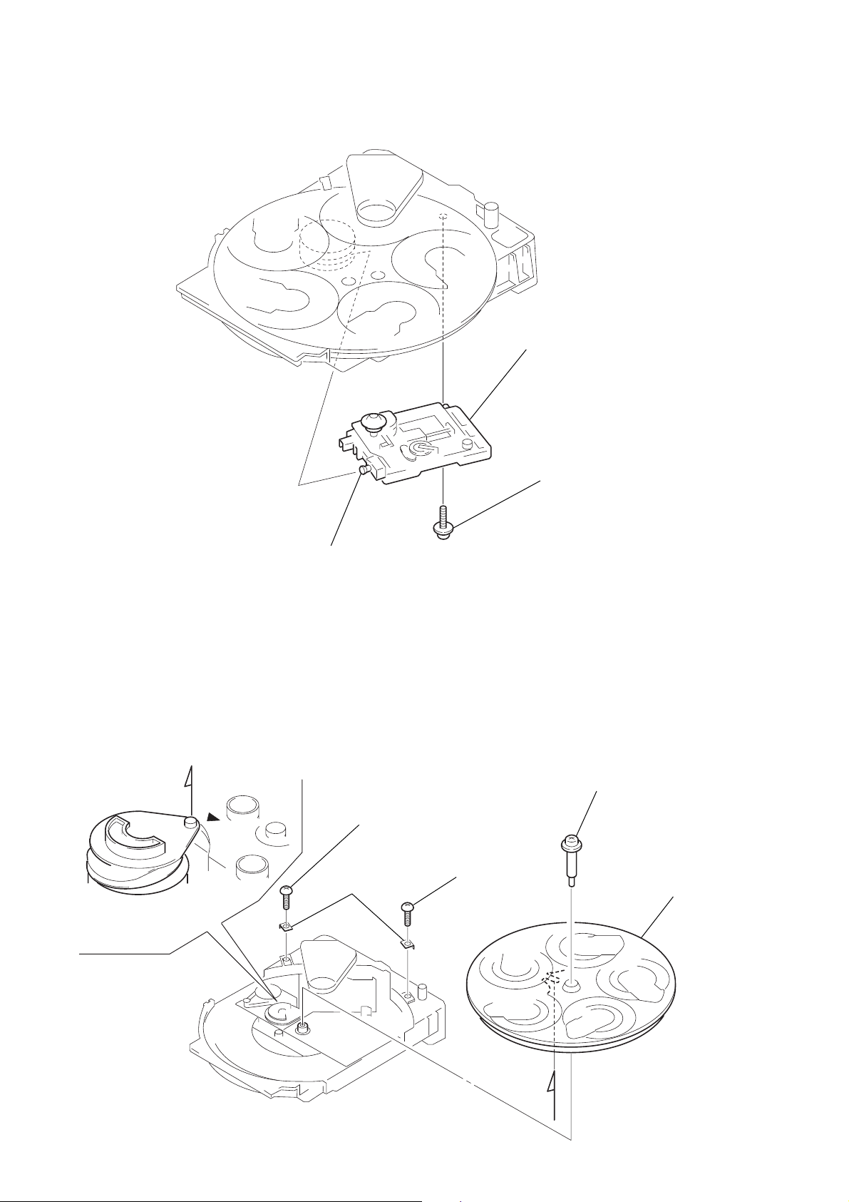
A

)
s
3-12. BD BOARD
1
5
Screw
(BVTP2.6 × 8)
6
Removal
the four solders.
Two screws
(PTPWH M2.6 × 8)
3
Two springs
1
Two screws
(PTPWH M2.6 × 8)
2
Optical pick-up
section
3
Two springs
4
Wire (flat type)
(16 core) (CN101
7
BD board
Limit switch
(S101)
3-13. OPTICAL PICK-UP (KSS-213D / Q-NP) , SLED MOTOR (M102) , SPINDLE MOTOR (M101)
3
Optical pick-up (KSS-213D/Q-NP)
6
Spindle motor
(M101)
4
Two screw
(P2 × 3)
2
Sled shaft
1
Claw
– 13 –
5
Sled motor
(M102)

3-14. AUDIO BOARD, CAPSTAN MOTOR (M1)
1
Connector
(CN651)
2
Four screws
(BTP2.6 × 4)
3
Removal the AUDIO board
to direction of the arrow A.
A
7
Removal the capstan motor (M1)
to direction of the arrow B.
4
Break the soldering
of motor lead.
6
Claw
B
5
Two screws
(BTP2.6 × 8)
8
Hang two belts.
– 14 –

SECTION 4
TEST MODE
[MC Cold Reset]
• The cold reset clears all data including preset data stored in the
RAM to initial conditions. Execute this mode when returning
the set to the customer.
Procedure:
1. Pr ess three buttons SPECTRUM ANALYZER , ENTER ,
and
DISC 1 simultaneously.
2. The fluorescent indicator tube becomes blank instantaneously,
and the set is reset.
[CD Delivery Mode]
• This mode moves the pickup to the position durable to vibration. Use this mode when returning the set to the customer after
repair.
Procedure:
1. Press I /u button to turn the set ON.
2. Press PLA Y MODE button and I /u button simultaneously .
3. A message “LOCK” is displayed on the fluorescent indicator
tube, and the CD delivery mode is set.
[MC Hot Reset]
• This mode resets the set with the preset data kept stored in the
memory. The hot reset mode functions same as if the power
cord is plugged in and out.
Procedure:
1. Pr ess three buttons SPECTRUM ANALYZER , ENTER ,
and DISC 2 simultaneously.
2. The fluorescent indicator tube becomes blank instantaneously,
and the set is reset.
[Sled Servo Mode]
• This mode can run the CD sled motor freely . Use this mode, for
instance, when cleaning the pickup.
Procedure:
1. Select the function “CD”.
2. Pr ess three buttons SPECTRUM ANALYZER , ENTER ,
and FUNCTION simultaneously.
3. The Sled Servo mode is selected, if “CD” is blanking on the
fluorescent indicator tube.
4. With the CD in stop status, press ) button in CD section
to move the pickup to outside track, or 0 button to inside
track.
5. To exit from this mode, perform as follows:
1) Move the pickup to the most inside track.
2) Press three buttons in the same manner as step 2.
Note:
• Always move the pickup to most inside track when exiting from this
mode. Otherwise, a disc will not be unloaded.
• Do not run the sled motor e xcessively , otherwise the gear can be chipped.
[Change-over of AM Tuner Step between 9kHz and 10kHz]
• A step of AM channels can be changed over between 9kHz and
10kHz.
Procedure:
1. Press I /u button to turn the set ON.
2. Select the function “TUNER”, and press TUNER/BAND
button to select the BAND “AM”.
3. Press I /u button to turn the set OFF.
4. Press ENTER and I /u buttons simultaneously, and the
display of fluorescent indicator tube changes to “AM 9k STEP”
or “AM 10k STEP”, and thus the channel ste p is changed over.
[LED and Fluorescent Indicator Tube All Lit, Key Check
Mode]
Procedure:
1. Press three buttons SPECTRUM ANALYZER , ENTER ,
and DISC 3 simultaneously.
2. LEDs and fluorescent indicator tube are all turned on.
Press DISC 2 button, and the key check mode is activated.
3. In the key check mode, the fluorescent indicator tube displays
“K 1 J0 V0”. Each time a button is pressed, “K”value increases. However, once a button is pressed, it is no long er taken
into account.
“J” Value increases lik e 1, 2, 3 ... if rotating ≠ AMS ±
knob in “+” direction, or it decreases like 0, 9, 8 ... if rotating
in “–” direction.
“V” Value increases like 1, 2, 3 ... if rotating VOLUME knob
in “+” direction, or it decreases like 0, 9, 8 ... if rotating in
“–” direction.
4. To exit from this mode, press three buttons in the same man-
ner as step 1, or disconnect the power cord.
– 15 –

[Aging Mode]
This mode can be used for operation check of CD section and tape
deck section.
• If an error occurred:
The aging operation stops.
• If no error occurs:
The aging operation continues repeatedly.
1. Aging Mode in CD Section
1-1. Operating Method of Aging Mode
1. Set discs in DISC 1 and DISC 3 trays.
2. Select the function “CD”.
3. Press three buttons SPECTRUM ANAL YZER , ENTER
, and KARAOKE PON/MPX simultaneously.
4. The aging mode is activated, if a roulette mark on the fluorescent indicator tube is blinking.
5. In the aging mode, the aging is executed in a sequence
given in “1-2. Operation during Aging Mode”.
The aging continues unless an alarm occurred.
6. To exit from the aging mode, press I /u button to turn
the set OFF.
• If a button other than buttons In CD section is pressed during
aging, the aging in the CD section is finished.
• To execute aging to the tape deck section successively, press
· button in the deck A.
“AGING” is displayed on the fluorescent indicator tube. (For
the aging in tape deck, see “2. Aging Mode in Tape Deck Section”.
2-2. Operation during Aging Mode
In the aging mode, the program is executed in the following sequence.
1. A tape on FWD side is played for one minute.
2. PAUSE STOP is made.
3. Recording is made for 3 minutes. (For the deck not having
the record function, the play is executed.)
4. FF is executed up to the end of tape.
5. A tape is reversed, and the tape on REV side is played for
one minute.
6. PAUSE STOP is made.
7. Recording is made for 3 minutes. (For the deck not having the record function, the play is executed.)
8. FF is executed up to the end of tape.
9. Steps 1 through 8 are executed for the other deck.
10. Steps 1 through 9 are repeated unless an alarm occurred.
2-3. Deck Selection Sequence
• During the aging mode, decks are selected in the following sequence:
Deck A (FWD) → Deck A (REV)
↑↓
Deck B (REV) ← Deck B (FWD)
1-2. Operation during aging Mode
In the aging mode, the program is executed in the following sequence.
1. The disc tray turns to select a disc. (For a disc selection sequence, see Section 1-3.)
2. TOC of disc is read .
3. The pickup accesses to the last track.
4. Steps 1 through 3 are repeated.
1-3. Disc Selection Sequence
• During the aging mode, discs are selected in the following se-
quence:
Disc 1 → Disc 3
↑ ↓
Disc 3 ← Disc 1
2. Aging Mode in Tape Deck Section
2-1. Operating Method of Aging Mode
1. Load a commercially available 10-minute tape into the
decks A and B respectively.
(If a 10-minute tape is not available, another tape may be
used but a cycle time will be longer.)
2. Select the function “TAPE”.
3. Rewind tapes in advance by pressing 0 button respec-
tively on decks A and B.
4. Press three buttons SPECTRUM ANALYZER ,
ENTER , and KARAOKE PON/MPX simultaneously.
5. Press · button on dec k A. (This button triggers the ag-
ing mode.)
6. The aging mode is activated if “ AGING A” is displa yed on
the fluorescent indicator tube.
7. In the aging mode, the aging is executed in a sequence
given in “2-2. Operation during Aging Mode”.
The aging continues unless an alarm occurred.
8. To exit from the aging mode, press I /u button to turn
the set OFF.
– 16 –

SECTION 5
MECHANICAL ADJUSTMENTS
SECTION 6
ELECTRICAL ADJUSTMENTS
PRECAUTION
1. Clean the following parts with a denatured-alcohol-moistened
swab:
record/playback heads pinch rollers
erase head rubber belts
capstan idlers
2. Demagnetize the record/playback head with a head demagnetizer.
3. Do not use a magnetized screwdriver for the adjustments.
4. After the adjustments, apply suitable locking compound to the
parts adjusted.
5. The adjustments should be performed with the rated power
supply voltage unless otherwise noted.
• Torque Measurement
• Tape Tension Measurement
• Tor que Measurement
Mode Torque Meter Meter Reading
Forward CQ-102C
Forward
Back Tension (0.026 – 0.082 oz•inch)
Reverse CQ-102RC
Reverse
Back Tension (0.026 – 0.082 oz•inch)
FF, REW CQ-201B
CQ-102C
CQ-102RC
36 to 61g•cm
(0.50 – 0.84 oz•inch)
2 to 6g•cm
36 to 61g•cm
(0.50 – 0.84 oz•inch)
2 to 6g•cm
61 to 143g•cm
(0.85 – 1.98 oz•inch)
0 dB=0.775 VTAPE DECK SECTION
1. Demagnetize the record/playback head with a head demagnetizer. (Do not bring the head demagnetizer close to the erase
head.)
2. Do not use a magnetized screwdriver for the adjustments.
3. After the adjustments, apply suitable locking compound to the
parts adjust.
4. The adjustments should be performed with the rated power
supply voltage unless otherwise noted.
5. The adjustments should be performed in the order given in
this service manual. (As a general rule, playback circuit adjustment should be completed before performing recording
circuit adjustment.)
6. The adjustments should be performed for both L-CH and Rch.
7. Switc hes and controls should be set as follows unless otherwise specified.
8. Set to test mode. (Press key switch same time
SPECTRUM ANALYZER , ENTER and EFFECT button.)
• Test T ape
Tape Signal Used for
P-4-A100 10 kHz, –10 dB Azimuth Adjustment
WS-48B 3 kHz, 0 dB Tape Speed Adjustment
P-4-L300 315 Hz, 0 dB Level Adjustment
Record/ Playback Head Azimuth Adjustment
• Tape T ension Measurement
Mode Tension Meter Meter Reading
Forward CQ-403A more than 100 g (3.52 oz)
Reverse CQ-403R more than 100 g (3.52 oz)
DECK A DECK B
Note: Perform this adjustments for both decks
Procedure:
test tape
P-4-A100
(10 kHz, –10 dB)
set
main board
CN207
3
(L-CH)
Pin
Pin
1
(R-CH)
main board
CN207
Pin
2
level meter
+
–
– 17 –

1. Mode: Playback (FWD)
e
2. Turn the adjustment screw and check output peaks. If the peaks
do not match for L-CH and R-CH, turn the adjustment screw
so that outputs match within 1dB of peak.
within
output
level
1dB
L-CH
peak
R-CH
peak
within
1dB
Screw
position
L-CH
peak
Screw
position
R-CH
peak
3. Mode: Playback (FWD)
test tape
P-4-A100
(10 kHz, –10 dB)
L-CH
main
board
CN207
set
R-CH
waveform of oscilloscope
in phase 45
pin
3
pin
L
R
1
pin
°
90 °135 °180
good
2
oscilloscope
V
°
wrong
H
4. Repeat steps 1 to 3 in playback (REV) mode.
5. After the adjustments, apply suitable locking compound to the
pats adjusted.
Adjustment Location: Record/Playback Head (Deck A and B)
and MAIN board.
Tape Speed Adjustment DECK A
Note: Start the Tape Speed adjustment as below after setting to the test
mode.
In the test mode, the tape speed is high during pressing the
H. SPEED DUBB button.
Procedure:
1. Turn the power switch on.
2. Press the SPECTRUM ANALYZER b utton, ENTER button
and EFFECT button simultaneously.
To exit from the test mode, press the I /u button.
Mode: Playback (FWD)
test tape
WS-48B
(3 kHz, 0 dB)
set
MAIN board
CN207 (Pin
(Pin
frequency counter
+
–
3
: L-CH)
1
:R-CH)
1. Insert the WS-48B into the deck A and the blank tape into the
deck B.
2. Press the REC button and · button on the dec k B. Then
the deck B is at recording mode.
3. Set the deck A to playback mode.
4. Keep pressing the H. SPEED DUBB button in playback mode.
Then at HIGH speed mode.
5. Adjust RV652 on the AUDIO board do that frequency counter
reads 6,000 ± 180 Hz.
6. Take off the H. SPEED DUBB button.
Then at NORMAL speed mode.
7. Adjust RV651 on the AUDIO board so that frequency counter
reads 3,000 ± 90 Hz.
8. Frequency difference between deck A and deck B the beginning of the tape should be within ± 1.5%.
Adjustment Location: AUDIO and MAIN boards
Sample Value of Wow and flutter: 0.3% or less W. RMS
(WS-48B)
Playback level Adjustment
DECK A DECK B
Procedure:
Mode: Playback (FWD)
test tape
P-4-L300
(315 Hz, 0 dB)
level meter
forward
3
1
+
–
: L-CH)
: R-CH)
revers
set
main board
CN207 (Pin
(Pin
Deck A is RV311 (L-CH) and RV411 (R-CH), Deck B is RV301
(L-CH) and RV401 (R-CH) so that adjustment within adjustment
level as follows.
Adjustment Level:
CN207 PB level: 301.5 to 338.3 mV (–8.2 to –7.2 dB) level
difference between the channels: within ± 0.5 dB
Adjustment Location: AUDIO and MAIN boards
– 18 –

Record bias Current Adjustment
r
r
CN207
CN205
RECORD
LEVEL
IC1501
RV1501
RV1551
31
Procedure:
1. Mode: Record
Pin
6
(L-CH) of IC1501 on the MAIN board.
Pin #¶ (R-CH) of IC1501 on the MAIN board.
1) 315 Hz
2) 10 kHz
AF OSC
attenuator
Pin 2 (GND) of CN207 on the MAIN
board.
50 mV (–23.8 dB)
600
Ω
2. Mode: Playback
recorded
portion
DECK B
set
level mete
Adjustment Location:
[MAIN BOARD] (Component Side)
blank tape
CN-123
3
1
+
–
: L-CH)
: R-CH)
set
CN207 (Pin
(Pin
Confirm playback the signal recorded in step 1 become adjustable
limits as follows.
If these levels do not adjustable limits, adjustment the RV341 (LCH) and RV441 (R-CH) on the AUDIO board to repeat steps 1
and 2.
Adjustable limits: Playback output of 315 Hz to playback output
of 10 kHz: 0 ± 0.5 dB
Adjustment Location: AUDIO and MAIN boards
Record Level Adjustment
DECK B
Procedure:
1. Mode: Record
Pin
6
(L-CH) of IC1501 on the MAIN board.
Pin #¶ (R-CH) of IC1501 on the MAIN board.
AF OSC
315 Hz, 50 mV (–23.8 dB)
600
attenuator
Ω
blank tape
CS-123
set
[AUDIO BOARD] (Conductor Side)
RECORD
BIAS CURRENT
L
R
RL
RV441
PB LEVEL
RV341
RV301
RV401
TAPE SPEED
(NORMAL) (HIGH)
PB
LEVEL
RV651
RV652
RV311 L
RV411 R
– DECK A –– DECK B –
* As the adjustment parts is mounted on the component side, ad-
just it through a hole in the A UDIO board form conductor side.
(Except RV431, 441)
2
(GND) of CN207 on the MAIN board.
Pin
2. Mode: Playback
recorded
portion
set
CN207 (Pin
(Pin
Confirm playback the signal recorded in step 1 become adjustable
limits as follows.
If these levels do not adjustable limits, adjustment the RV1501
3
1
: L-CH)
: R-CH)
level mete
+
–
(L-CH) and RV1551 (R-CH) on the MAIN board to r epeat steps 1
and 2.
Adjustable limits:
CN207 PB level: 36.7 to 41.1 mV (–26.5 to –25.5 dB)
Adjustment Location: MAIN board
– 19 –

CD SECTION
V
V
Note:
1. CD Block is basically designed to operate without adjustment. Therefore, check each item in order given.
2. Use YEDS-18 disc (3-702-101-01) unless otherwise indicated.
3. Use an oscilloscope with more than 10M impedance.
4. Clean the object lens by an applicator with neutral detergent when the
signal level is low than specified value with the following checks.
Focus Bias check
oscilloscope
BD board
TP (FEO)
TP (VC)
Procedure:
1. Connect oscilloscope to test point TP (RF). (GND terminal:
VC)
2. Turned Power switch on.
3. Put disc (YEDS-18) in and playback.
4. Confirm that the shape “≈” can be clearly distinguished at the
center of the waveform and check the RF signal level.
• RF signal
+
–
S Curve Check
oscilloscope
BD board
TP (FEO)
TP (VC)
+
–
Procedure:
1. Connect oscilloscope to test point TP (FEO).
2. Connect between test point TP (FOK) and GND by lead wire.
3. Turn Power switch on.
4. Put disc (YEDS-18) in and turned Power switch on again and
actuate the focus search. (actuate the focus search when disc
table is moving in and out.)
5. Chec k the oscilloscope waveform (S-curve) is symmetrical
between A and B. And confirm peak to peak level within
3 ± 1 Vp-p.
S-curve waveform
symmetry
A
within 3
±
1 Vp-p
B
VOLT/DIV: 200 m
TIME/DIV: 500 ns
level:
±
0.3 Vp-p
1.3
6. After check, remove the lead wire connected in step 2.
Note: •Try to measure several times to make sure than the ratio of A : B
or B : A is more than 10 : 7.
• Tak e sweep time as long as possible and light up the brightness to
obtain best waveform.
RF Level Check
oscilloscope
BD board
TP (RF)
TP (VC)
+
–
Procedure:
1. Connect oscilloscope to test point TP (TEO) on BD board.
2. Turned Power switch on.
3. Put disc (YEDS-18) in to play the number five track.
4. Confirm that oscilloscope waveform is clear and check RF
signal level is correct or not.
• SF signal
VOLT/DIV: 200 m
TIME/DIV: 500 ns
level:
±
0.3 Vp-p
1.3
Note: Clear RF signal wavefor m means that the shape “≈” can be clearly
distinguished at the center of the waveform.
– 20 –

E-F Balance (1 Track Jump) check
)
(Without remote commander)
oscilloscope
BD board
TP (TEO)
TP (VC)
+
–
Procedure:
1. Connect oscilloscope to test point TP (TEO) on BD board.
2. Turned Power switch on.
3. Put disc (YEDS-18) in to play the number five track.
4. Press the “P (Pause)” button. (Becomes the 1 track jump
mode)
5. Chec k the level B of the oscilloscope’s waveform and the A
(DC voltage) of the center of the Traverse waveform.
Confirm the following:
Adjustment Location:
[BD BOARD] (Conductor Side)
RF
IC101
CNU101
TEO
GND
FEO
IC103
FOK
VC
IC
I02
A – B
2 (A + B)
1 track jump waveform
0V
level : 500 mV
× 100 = ±7 (%)
±
100 mVp-p
Center of the waveform
B
A (DC voltage
symmetry
CNU102
– 21 –

SECTION 7
DIAGRAMS
7-1. IC PIN FUNCTION DESCRIPTION
• MAIN BOARD IC301 µPD780018YGF-028-3BA (SYSTEM CONTROLLER)
Pin No. Pin Name I/O Function
1 TA-MUTE O
2 DBFB-H/L O
3 427-LAT O
4 K-CON-LAT O
5 K-CON-ON O
6 F-RELAY O
7 R-RELAY O
8 PL-RELAY O
9 TEST I
10 X2 O
11 X1 I
12 VDD —
13 XT2 O
14 XT1 I
15 RESET I
16 (INT/IN) I
17 (INT/IN/OUT) I
18 SCOR I
19 SOFT-TEST O
20 AC-CUT I
21 RDS-INT I
22 RDS-DATA I
23 VDD —
24 AVDD —
25 ADJ I
26 A-SHUT I
27 B-SHUT I
28 B-HALF I
29 CLK-CHECK I
30 SPEC-IN I
31 ADJ2 I
32 DEMO-MODE I
33 AVSS —
34 SQ-DATA-IN I
35 NCO O
36
37
38
39 FUNC2 I
40 VSS —
41 VOL-LAT O
42 PL-LAT O
43 COM-DIN I
SQ-CLK
SW-ON/OFF
FUNC1
Line muting on/off control signal output terminal “L”: muting on
DBFB normal/high selection signal output to the M62427FP (IC201)
“L”: DBFB high, “H”: DBFB low
Serial data latch pulse output to the M62427FP (IC201)
Serial data latch pulse output terminal Not used (open)
On/off selection signal output of the key control circuit “L”: on Not used (open)
Relay drive signal output for the speaker protect “H”: on
Relay drive signal output for the speaker protect “H”: on Not used (open)
Relay drive signal output for the speaker protect “H”: on Not used (open)
Test terminal Connected to ground
Main system clock output terminal (5 MHz)
Main system clock input terminal (5 MHz)
Power supply terminal (+5V)
Sub system clock output terminal (32.768 kHz)
Sub system clock input terminal (32.768 kHz)
System reset signal input from the reset signal generator (IC302) “L”: reset
For several hundreds msec. after the power supply rises, “L” is input, then it changes to “H”
Connected to ground
Connected to ground
Subcode sync (S0+S1) detection signal input from the CXD2519Q (IC103)
Output terminal for the software test (open)
AC off detection signal input from the reset signal generator (IC302)
Serial data reading clock signal input for the radio data system Not used (fixed at “L”)
Serial data input for the radio data system Not used (open)
Power supply terminal (+5V)
Power supply terminal (+5V) (for A/D conversion)
Setting terminal for the CD test mode Normally: fixed at “H”
Shut off detection signal input from the deck-A side reel pulse detector (Q1001)
Shut off detection signal input from the deck-B side reel pulse detector (Q1002)
Detection input from the deck-B half detect switch (S1006)
Not used (fixed at “L”)
Setting terminal for the version
Setting terminal for the CD test mode Normally: “L”
Setting terminal for the demonstration H/L Fixed at “L”
Ground terminal (for A/D conversion)
Sub-code Q data input from the CXD2519Q (IC103)
Not used (open)
O
Sub-code Q data reading clock signal output to the CXD2519Q (IC103)
O
Super woofer speaker on/off control signal output terminal Not used (open)
I
Setting terminal for the function 1 Fixed at “L”
Setting terminal for the function 2 Fixed at “L”
Ground terminal
Serial data latch pulse output terminal Not used (open)
Serial data latch pulse output terminal Not used (open)
Serial data input terminal Not used (fixed at “L”)
– 22 –

Pin No. Pin Name I/O Function
44 COM-DOUT O
45 COM-CLK O
46 CD-POWER O
47 CD-DATA O
48 CD-CLK O
49 MSM-CND O
50 MSM-BUSY I
51 MSM-LAT O
52 MSM-NAR O
53 MSM-CH O
54
55 IIC-DATA I/O
56 IIC-CLK I/O
57 XRST O
58 XLT O
59 WDCL O
60 TBL-L O
61 TBL-R O
62 TRAY-LED O
63 LOAD-OUT O
64 LOAD-IN O
65 ST-CLK O
66 ST-DIN I
67 ST-DOUT O
68 ST-CE O
69 TUNED I
70 STEREO I
71 VSS —
72 ST-MUTE O
73 SENS2 I
74 SENS I
75 DISC-SENS I
76 T-SENS I
77 UP SW I
78 ENC3 I
79 ENC2 I
80 ENC1 I
81 OUT-OPEN I
82 CAP-H/N O
83 A-TRG O
84 B-TRG O
85 TRG-LOW O
INPUT-
CHANGE
Serial data output to the M62427FP (IC201)
Serial data transfer clock signal output to the M62427FP (IC201)
Power on/off control signal output for the CD mechanism deck section
“H”: power on, “L”: standby
Serial data output to the CXD2519Q (IC103)
Serial data transfer clock signal output to the CXD2519Q (IC103)
Command data output terminal Not used (open)
Busy signal input terminal “L”: busy status Not used (fixed at “L”)
Serial data latch pulse output terminal Not used (open)
NAR signal output terminal Not used (open)
Channel select signal output terminal Not used (open)
Attenuate control (–5 dB) signal output for the input gain control
O
“L”: VIDEO, “H”: MD
Communication data bus with the fluorescent indicator tube driver (IC601)
Communication data reading clock signal input or transfer clock signal output with the fluo-
rescent indicator tube driver (IC601)
Reset signal output to the CXA1992AR (IC101), BA5941FP (IC102) and CXD2519Q (IC103) on
the CD mechanism deck section “L”: reset
Serial data latch pulse output to the CXD2519Q (IC103)
Word clock signal output terminal Not used (open)
Motor drive signal output to the disc tray turn motor driver (IC201) *1
Motor drive signal output to the disc tray turn motor driver (IC201) *1
LED drive signal output for the CD tray LED indicate “H”: LED on
Motor drive signal output terminal Not used (open)
Motor drive signal output terminal Not used (open)
PLL serial data transfer clock signal output to the FM/AM tuner unit
PLL serial data input from the FM/AM tuner unit
PLL serial data output to the FM/AM tuner unit
PLL chip enable signal output to the FM/AM tuner unit
Tuning detection signal input from the FM/AM tuner unit “L”: tuned
FM stereo detection signal input from the FM/AM tuner unit “L”: stereo
Ground terminal
Tuner muting control signal output to the FM/AM tuner unit “L”: muting on
Internal status (SENSE) signal input from the CXA1992AR (IC101)
Internal status (SENSE) signal input from the CXD2519Q (IC103)
Disc status detection signal input terminal Not used (open)
Disc tray status detection signal input from the disc tray sensor (IC202)
Detection input from the UP switch (S201)
Rotary encoder pulse input for the disc tray address detect Not used (open)
Disc tray open/close detect switch input terminal “L”: open, “H”: close Not used (open)
High/normal speed selection signal output of the capstan motor (M1)
“L”: high speed, “H”: normal speed
Motor drive signal output to the trigger motor driver (IC1502)
Motor drive signal output to the trigger motor driver (IC1502)
Motor control signal output to the trigger motor driver (IC1502)
– 23 –

Pin No. Pin Name I/O Function
86 CAP-M-ON/OFF O
87 PB-A/B O
88 EQ-H/N O
89 BIAS O
90 REC-MUTE O
91 NR-ON/OFF O
92 R/P-PASS O
93 TC-MUTE O
94 A-PLAY-SW I
95 B-PLAY-SW I
96 RELAY O
97 A-HALF I
98 POWER O
99 SW-F-CON O
100 STK-MUTE O
Capstan motor (M1) on/off control signal output terminal “L”: capstan motor on
Deck-A/B selection signal output to the HA12203NT (IC1501) “L”: deck-A, “H”: deck-B
Normal/high speed selection signal output to the HA12203NT (IC1501)
“L”: normal speed, “H”: high speed
Recording bias on/off selection signal output to the HA12203NT (IC1501)
“L”: bias off, “H”: bias on
Recording muting on/off selection signal output to the HA12203NT (IC1501)
“L”: muting on, “H”: muting off
Dolby NR on/off selection signal output to the HA12203NT (IC1501)
“L”: dolby off, “H”: dolby on
Recording/playback/pass selection signal output to the HA12203NT (IC1501)
“L”: recording mode
Line muting on/off selection signal output to the HA12203NT (IC1501)
“L”: muting off, “H”: muting on
Detection input from the deck- A play detect switch (S1001) “H”: deck-A play
Detection input from the deck- B play detect switch (S1002) “H”: deck-B play
Recording/playback select signal output to the REC/PB switch (IC602)
“L”: playback, “H”: recording
Detection input from the deck-A cassette detect switch (S1003)
“L”: cassette in, “H”: no cassette
Power on/off control signal output for the audio system (+5V) and deck, panel, audio system
(+7V and –7V) “L”: power on, “H”: standby
Super woofer mode control signal output to the M62427FP (IC201) “H”: music, “L”: movie
Power amplifier on/off selection signal output terminal “L”: on, “H”: standby
*1 Disc tray turn motor (M201) control
Mode
Terminal
TBL-L (pin ^º)
TBL-R (pin ^¡)
STOP
“H” “L” “H” “L”
“H” “H” “L” “L”
COUNTER-
CLOCKWISE
CLOCKWISE BRAKE
– 24 –
 Loading...