

Page 1
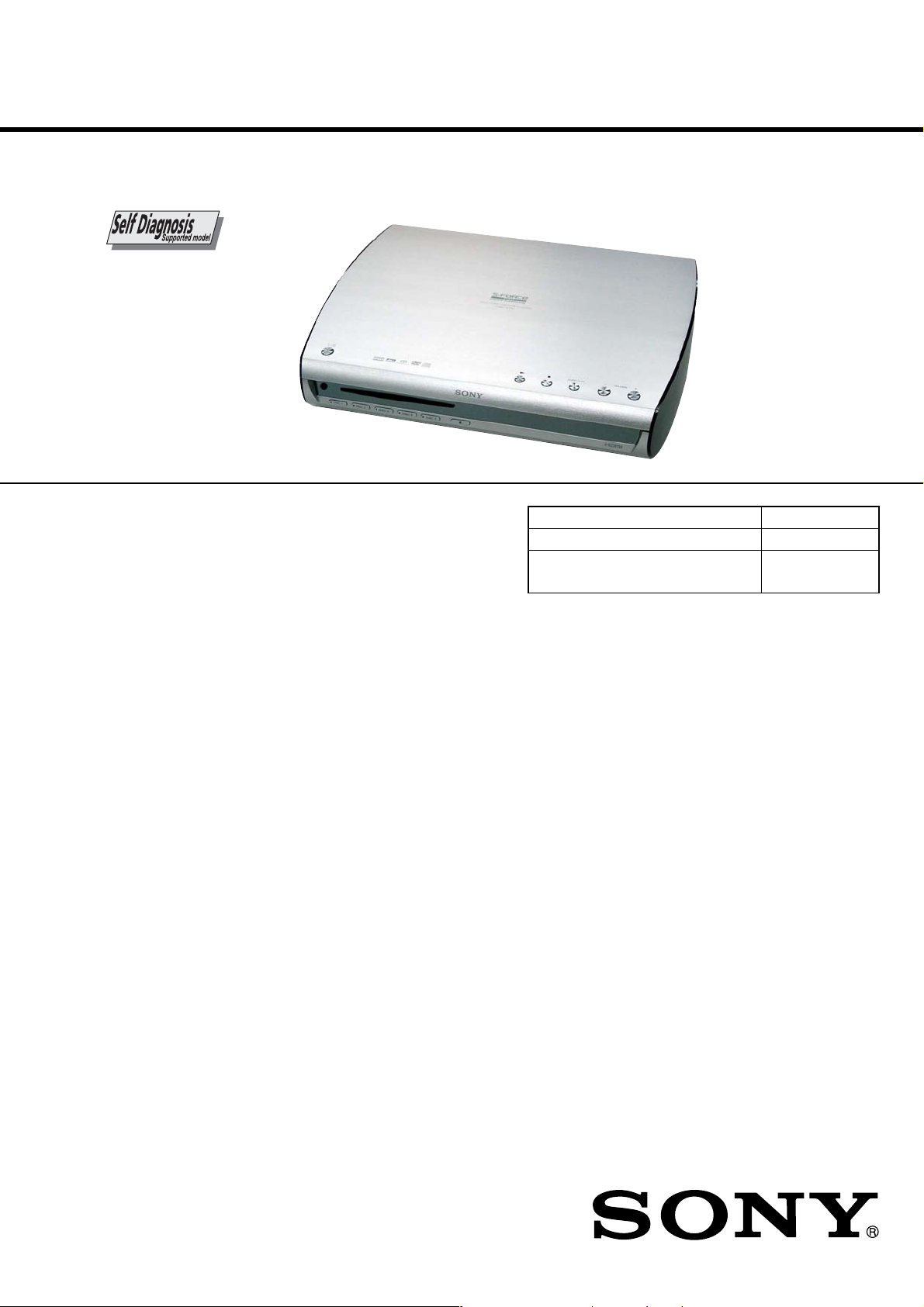
HCD-X1V
SERVICE MANUAL
Ver. 1.0 2006.07
• HCD-X1V is the amplifier, super audio CD/DVD
system, tuner and video section in DAV-X1V.
This system incorporates with Dolby* Digital
and Dolby Pro L ogic (II) ada p tive matrix
surround decoder and the DTS** Digital
Surround System.
This system perfectly decodes 5.1 channel
signal, but you cannot add other com mercially
available surround speakers.
*Manufactured under license from Dolby
Laboratories.
“Dolby”, “Pro Logic”, and the double-D symbol are
trademarks of Dolby Laboratories.
**Manufactured under license from Digital Theater
Systems, Inc. “DTS” and “DTS Digital Surround”
are registered trademarks of Digital Theater
Systems, Inc.
AUDIO POWER SPECIFICATIONS
for the US model
POWER OUTPUT AND
TOTAL HARMONIC
DISTORTION
(FTC Output Power): Front: 38 W/ch 4 ohms at
Amplifier section
Front
Power output (rated): 70 W + 70 W (4 ohms,
RMS output power
Front surround*
Power output (rated): 70 W + 70 W (4 ohms,
RMS output power
Subwoofer
Power output (rated): 70 W + 70 W (4 ohms,
RMS output power
* Depending on the sound field settings and the source,
there may be no sound output.
150 -20,000 Hz,
0.7% THD
Front surround: 38 W/ch
4 ohms at 150 -20,000 Hz,
0.7% THD
Subwoofer: 38 W/ch
4 ohms at 25 - 150 Hz,
0.7 % THD
1 kHz, 1 % THD)
(reference):
80 W + 80 W (4 ohms,
1 kHz, 10 % THD)
1 kHz, 1 % THD)
(reference):
80 W + 80 W (4 ohms,
1 kHz, 10 % THD)
100 Hz, 1 % THD)
(reference):
80 W + 80
100 Hz, 10 % THD)
US Model
Canadian Model
AEP Model
UK Model
Model Name Using Similar Mechanism NEW
DVD Mechanism Type CDM69EH
Optical Pick-up Block Name KHM-310CAB or
KHM-313CAB
SPECIFICATIONS
Inputs (Analog)
W (4 ohms,
VIDEO1, VIDEO2, TV, AUDIO IN
Inputs (Digital/COAXIAL)
VIDEO1 , VIDEO2 Impedance: 75 ohms
Super Audio CD/DVD system
Laser Semiconductor laser
Signal format system
For North American models:
For European models: NTSC/PAL
Tuner section
System PLL quartz-locked digital
FM tuner section
Tuning range
For North American models:
For European models: 87.5 – 108.0 MHz
Antenna (aerial) FM wire antenna (aerial)
Antenna (aerial) terminals 75 ohms, unbalanced
Intermediate frequency 10.7 MHz
Sensitivity: 450 mV (ATT
ON), 250 mV (ATT OFF)
Impedance: 50 kilohms
(Super Audio CD/DVD:
λ = 650 nm)
(CD:λ = 790 nm)
Emission duration:
continuous
NTSC
synthesizer system
87.5 – 108.0 MHz
(100 kHz step)
(50 k Hz step)
– Continued on next page –
9-887-304-01
2006G05-1
© 2006.07
SUPER AUDIO CD/DVD RECEIVER
Sony Corporation
Home Audio Division
Published by Sony Techno Create Corporation
Page 2
HCD-X1V
r
AM tuner section
Tuning range
For North American models:
For European models: 531 – 1,602 kHz (with the
Antenna (aerial) AM loop antenna (aerial)
Intermediate frequency 450 kHz
Video section
Outputs VIDEO: 1 Vp-p 75 ohms
Inputs VIDEO: 1 Vp-p 75 ohms
General
Power requirements
For North American models:
For European models: 230 V AC, 50 Hz
Power consumption On: 165 W
Dimensions (approx.) 413 × 90 × 325 mm
Mass (approx.) 5.5 kg (12 lb 3 oz)
Design and specifications are subject to change
without notice.
530 – 1,710 kHz (with the
interval set at 10kHz)
531 – 1,710 kHz (with the
interval set at 9 k Hz)
interval set at 9 k Hz)
S VIDEO:
Y: 1 V p-p 75ohms
C: 0.286 V p-p 75ohms
COMPONENT:
Y: 1 Vp-p 75 ohms
PB/CB, PR/CR: 0.7 V p-p
75 ohms
HDMI OUT: Type A (19
pin)
S VIDEO:
Y: 1 Vp-p 75 ohms
C: 0.286 V p-p 75 ohms
120 V AC, 60 Hz
Standby: 0.3 W (at the
Power Saving mode)
3
(16
/8 × 3 5/8 × 12 7/
inches) (w/h/d) incl.
projecting parts
8
Notes on chip component replacement
• Never reuse a disconnected chip component.
• Notice that the minus side of a tantalum capacitor may be
damaged by heat.
Flexible Circuit Board Repairing
• Keep the temperature of the soldering iron around 270 ˚C
during repairing.
• Do not touch the soldering iron on the same conductor of the
circuit board (within 3 times).
• Be careful not to apply force on the conductor when soldering
or unsoldering.
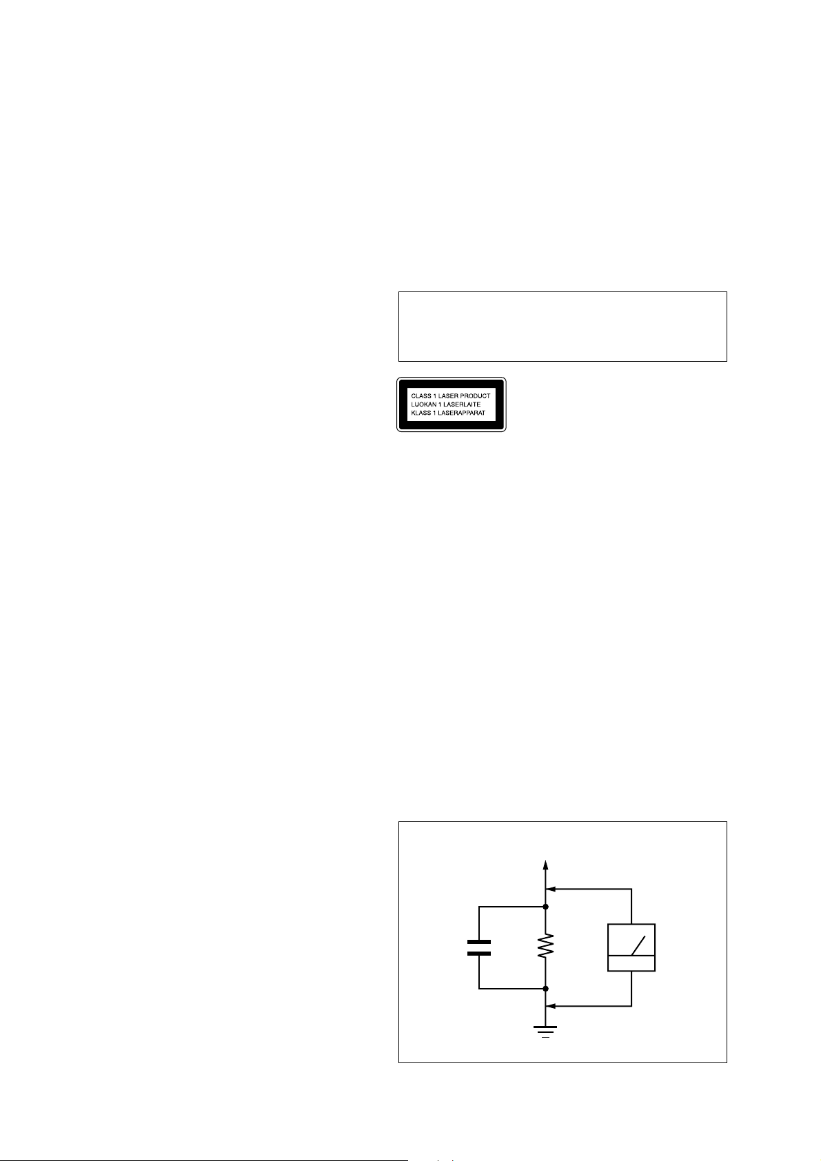
CAUTION
Use of controls or adjustments or performance of procedures
other than those specified herein may result in hazardous radiation
exposure.
This appliance is
classified as a CLASS 1
LASER product. This
marking is located on the
rear or bottom exterior.
SAFETY CHECK-OUT
After correcting the original service problem, perform the following
safety check before releasing the set to the customer:
Check the antenna terminals, metal trim, “metallized” knobs, screws,
and all other exposed metal parts for AC leakage.
Check leakage as described below.
LEAKAGE TEST
The AC leakage from any exposed metal part to earth ground and
from all exposed metal parts to any exposed metal part having a
return to chassis, must not exceed 0.5 mA (500 microamperes.).
Leakage current can be measured by any one of three methods.
1. A commercial leakage tester, such as the Simpson 229 or RCA
WT -540A. Follow the manuf acturers’ instructions to use these
instruments.
2. A battery-operated AC milliammeter. The Data Precision 245
digital multimeter is suitable for this job.
3. Measuring the voltage drop across a resistor by means of a
VOM or battery-operated A C voltmeter . The “limit” indication
is 0.75 V, so analog meters must have an accurate low-v oltage
scale. The Simpson 250 and Sanwa SH-63Trd are examples
of a passive VOM that is suitable. Nearly all battery operated
digital multimeters that have a 2 V A C range are suitable. (See
Fig. A)
SAFETY-RELATED COMPONENT WARNING!!
COMPONENTS IDENTIFIED BY MARK 0 OR DOTTED LINE
WITH MARK 0 ON THE SCHEMATIC DIAGRAMS AND IN
THE PARTS LIST ARE CRITICAL TO SAFE OPERATION.
REPLACE THESE COMPONENTS WITH SONY PARTS WHOSE
PART NUMBERS APPEAR AS SHOWN IN THIS MANU AL OR
IN SUPPLEMENTS PUBLISHED BY SONY.
ATTENTION AU COMPOSANT AYANT RAPPORT
À LA SÉCURITÉ!
LES COMPOSANTS IDENTIFIÉS P AR UNE MARQ UE 0 SUR
LES DIAGRAMMES SCHÉMATIQUES ET LA LISTE DES
PIÈCES SONT CRITIQUES POUR LA SÉCURITÉ DE
FONCTIONNEMENT. NE REMPLACER CES COM- POSANTS
QUE PAR DES PIÈCES SONY DONT LES NUMÉROS SONT
DONNÉS DANS CE MANUEL OU D ANS LES SUPPLÉMENTS
PUBLIÉS PAR SONY.
2
To Exposed Metal
Parts on Set
AC
1.5 k
0.15 µF
Ω
voltmete
(0.75 V)
Earth Ground
Fig. A. Using an AC voltmeter to check AC leakage.
Page 3

HCD-X1V
SELF DIAGNOSIS FUNCTION
(When letters/numbers appear in the
display)
When the self-diagnosis function is activated to
prevent the system from malfunctioning, a 5character service number (e.g., C 13 50) with a
combination of a letter and 4 digits appears on
the screen and the front panel display. In this
case, check the following table.
C:13:50
First 3
character s of
the service
number
C 13 The disc is dirty.
C 31 The disc is not inserted correctly.
E XX
(xx is a number)
Cause and/or corrective action
,Clean the disc with a soft cloth.
,Restart the system, then re-insert
the disc correctly.
To prevent a malfunction, the
system has performed the selfdiagnosis function.
,Contact your nearest Sony
dealer or local authorized Sony
service facility and give the 5character service number.
Example: E 61 10
TABLE OF CONTENTS
1. SERVICING NOTES............................................... 4
2. GENERAL ................................................................... 11
3. DISASSEMBLY
3-1. Disassembly Flow ........................................................... 13
3-2. Top Panel, Side Panel ...................................................... 14
3-3. DMB12 Board ................................................................. 14
3-4. POWER Board ................................................................ 15
3-5. AMP Board...................................................................... 15
3-6. Rear Panel Block ............................................................. 16
3-7. MAIN Board.................................................................... 16
3-8. DVD Mechanism deck (CDM69EH) .............................. 17
3-9. Optical Pick-Up Section.................................................. 17
3-10. Optical Pick-Up Block
(KHM-310CAB or KHM-313CAB) ............................... 18
3-11. Bracket (Top) Assy .......................................................... 18
3-12. RELAY Board ................................................................. 19
3-13. Motor (Stocker) Assy (Stocker) (M761) ......................... 19
3-14. Motor (Stocker) Assy (Roller) (M781) ........................... 20
3-15. Motor (Stocker) Assy (Mode) (M771) ............................ 20
3-16. Rubber Roller (Silder) Assy, Sub Chassis....................... 21
3-17. Timing Belt (Front/Rear) ................................................. 21
3-18. Cam (Gear) ...................................................................... 22
3-19. SENSOR Board, Rotary Encoder (Mode) (S771) ........... 22
4. ASSEMBLY
4-1. How To Install The Cam (Eject Lock) ............................ 23
4-2. How To Install The Cam (Gear) ...................................... 23
4-3. How To Install The Gear (Mode C)................................. 24
4-4. How To Install The Gear (Mode Cam)............................ 24
4-5. How To Install The Rotary Encoder (S702),
Gear (Stocker Communication)....................................... 25
4-6. How To Install The Cam (Stocker U/D) .......................... 25
4-7. How To Install The Stocker Assy .................................... 26
4-8. Phase Adjustment Between Pinions (Slider)
And Slider-1 To 5 (L/R) .................................................. 27
5. TEST MODE.............................................................. 28
6. ELECTRICAL CHECK........................................... 31
7. DIAGRAMS
7-1. Block Diagram – RF SERVO/VIDEO Section – ............ 32
7-2. Block Diagram – CHANGER/HDMI Section – ............. 33
7-3. Block Diagram – AUDIO Section –................................ 34
7-4. Block Diagram – AMP Section – .................................... 35
7-5. Block Diagram
– PANEL/POWER SUPPLY Section – ........................... 36
7-6. Printed Wiring Board – DMB12 Board (Side A) – ......... 38
7-7. Printed Wiring Board – DMB12 Board (Side B) – ......... 39
7-8. Schematic Diagram – DMB12 Board (1/6) –.................. 40
7-9. Schematic Diagram – DMB12 Board (2/6) –.................. 41
7-10. Schematic Diagram – DMB12 Board (3/6) – .................. 42
7-11. Schematic Diagram – DMB12 Board (4/6) – .................. 43
7-12. Schematic Diagram – DMB12 Board (5/6) – .................. 44
7-13. Schematic Diagram – DMB12 Board (6/6) – .................. 45
7-14. Printed Wiring Boards – CHANGER Section –.............. 46
7-15. Schematic Diagram – CHANGER Section – .................. 47
7-16. Printed Wiring Boards – D-IO/AUDIO IN Boards – ...... 48
7-17. Schematic Diagram – D-IO Board – ............................... 49
7-18. Printed Wiring Board
– MAIN Board (Component Side) – ............................... 50
3
Page 4

HCD-X1V
SECTION 1
SERVICING NOTES
7-19. Printed Wiring Board
– MAIN Board (Conductor Side) – ................................. 51
7-20. Schematic Diagram – MAIN Section (1/6) – .................. 52
7-21. Schematic Diagram – MAIN Section (2/6) – .................. 53
7-22. Schematic Diagram – MAIN Section (3/6) – .................. 54
7-23. Schematic Diagram – MAIN Section (4/6) – .................. 55
7-24. Schematic Diagram – MAIN Section (5/6) – .................. 56
7-25. Schematic Diagram – MAIN Section (6/6) – .................. 57
7-26. Printed Wiring Board
– AMP Board (Component Side) – ................................. 58
7-27. Printed Wiring Board
– AMP Board (Conductor Side) – ................................... 59
7-28. Schematic Diagram – AMP Board (1/3) – ...................... 60
7-29. Schematic Diagram – AMP Board (2/3) – ...................... 61
7-30. Schematic Diagram – AMP Board (3/3) – ...................... 62
7-31. Schematic Diagram – KEY Section – ............................. 63
7-32. Printed Wiring Board – LED Board – ............................. 64
7-33. Printed Wiring Boards – KEY/POWER-SW Boards – ... 65
7-34. Printed Wiring Board – DISPLAY Board – .................... 66
7-35. Schematic Diagram – DISPLAY Board – ....................... 67
7-36. Printed Wiring Board
– POWER Board (Component Side) –............................ 68
7-37. Printed Wiring Board
– POWER Board (Conductor Side) –.............................. 69
7-38. Printed Wiring Board – LF Board – ................................ 70
7-39. Schematic Diagram – POWER SUPPLY Section – ........ 71
8. EXPLODED VIEWS
8-1. Front/Side/Top Panel Section .......................................... 98
8-2. MAIN Board Section....................................................... 99
8-3. POWER Board Section .................................................. 100
8-4. DVD Mechanism Deck section-1 (CDM69EH)............. 101
8-5. DVD Mechanism Deck section-2 (CDM69EH)............. 102
8-6. DVD Mechanism Deck section-3 (CDM69EH)............. 103
8-7. DVD Mechanism Deck section-4 (CDM69EH)............. 104
8-8. DVD Mechanism Deck section-5 (CDM69EH)............. 105
8-9. DVD Mechanism Deck section-6 (CDM69EH)............. 106
8-10. Optical Pick-Up Section
(KHM-310CAB or KHM-313CAB) .............................. 107
NOTES ON HANDLING THE OPTICAL PICK-UP
BLOCK OR BASE UNIT
The laser diode in the optical pick-up block may suffer electrostatic
break-down because of the potential difference generated by the
charged electrostatic load, etc. on clothing and the human body.
During repair, pay attention to electrostatic break-down and also
use the procedure in the printed matter which is included in the
repair parts.
The flexible board is easily damaged and should be handled with
care.
NOTES ON LASER DIODE EMISSION CHECK
The laser beam on this model is concentrated so as to be focused on
the disc reflective surface by the objective lens in the optical pickup block. Therefore, when checking the laser diode emission,
observe from more than 30 cm away from the objective lens.
UNLEADED SOLDER
Boards requiring use of unleaded solder are printed with the leadfree mark (LF) indicating the solder contains no lead.
(Caution: Some printed circuit boards may not come printed with
the lead free mark due to their particular size)
: LEAD FREE MARK
Unleaded solder has the following characteristics.
• Unleaded solder melts at a temperature about 40 °C higher
than ordinary solder.
Ordinary soldering irons can be used but the iron tip has to be
applied to the solder joint for a slightly longer time.
Soldering irons using a temperature regulator should be set to
about 350 °C.
Caution: The printed pattern (copper foil) may peel away if
the heated tip is applied for too long, so be careful!
• Strong viscosity
Unleaded solder is more viscou-s (sticky, less prone to flow)
than ordinary solder so use caution not to let solder bridges
occur such as on IC pins, etc.
• Usable with ordinary solder
It is best to use only unleaded solder but unleaded solder may
also be added to ordinary solder.
9. ELECTRICAL PARTS LIST............................... 108
RELEASING THE TRAY LOCK
The disc tray lock function for the antitheft of an demonstration
disc in the store is equipped.
Releasing Procedure :
1. Press the I/1 button to turn on the system.
2. Press the FUNCTION button repeatedly to select “DVD”.
3. While pressing the x button, press the Z button until
“UNLOCKED” displayed on the fluorescent indicator tube
(around 5 seconds).
Note: When “LOCKED” is displayed, the tray lock is not released by turning
power on/off with the I/1 button.
RELEASING THE DEMO PLAY LOCK
Releasing Procedure :
1. Press the I/1 button to turn on the system.
2. Press the FUNCTION button repeatedly to select “DVD”.
3. While pressing the x button, press the N button until
“DEMO OFF” displayed on the fluorescent indicator tube
(around 5 seconds).
Note: When “DEMO PLAY” is displayed, the DEMO play lock is not
released by turning power on/off with the I/1 button.
4
Page 5
HCD-X1V
NOTE OF REPLACING THE EEPROM (IC103 and
IC706) ON THE DMB12 BOARD
EEPROM (IC103 and IC706) on the DMB12 board cannot exchange
with single. When EEPROM (IC103 and IC706) on the DMB12
board is damaged, exchange the entire mounted board.
NOTE OF HANDLING THE DMB12 BOARD
When the DMB12 board is replaced by a repair for a fee, throw
away the DMB12 board after obtaining consent of not returning of
the DMB12 board to the customer. When throwing awa y the DMB12
board, be sure to throw away after destroying EEPROM (IC103
and IC706) physically with the hammer etc.
Part No. Destination
A-1212-048-A US, Canadian
A-1212-049-A AEP, UK
MODEL IDENTIFICATION
– Back Panel –
PART No.
MODEL PART No.
US model 2-647-349-0[]
Canadian model 2-647-349-1[]
AEP and UK models 2-647-349-2[]
S-FORCE FRONT SURROUND OPERATION CHECK
When complaint by the effect of the sound field, check as follows
and confirm abnormality is not found in the set.
Procedure:
1
Press [/1.
The system turns on.
Unless the system is set to “DVD,” press
FUNCTION +/– to select “DVD.”
2
Press DISC 1.
3
Press Z.
4
Load the Setup Disc.
Push the disc into the disc slot until the disc
is pulled in automatically.
The Setup Disc is drawn into the system
automatically.
With the playback side facing down
e Setup Disc menu appears.
Th
DAV-X1 Series
This setup disc is common for DAV-X1 series.
5
Sit in the listening position, then select
one of the three options on the screen
using
C/c
, and press H or .
The selected option starts.
C
FL FR
SW
RL RR
6
Listening carefully to how the option
sounds to determine the optimal
surround sound effect.
If a satisfactory surround sound effect
cannot be achieved, adjust the speaker
positions.
7
Press x to stop the disc.
8
Press Z on the system to eject the
disc.
5
Page 6
HCD-X1V
About This Manual
•The instructions in this manual describe the
controls on the remote. You can also use the
controls on the system if they hav e the same o r
similar names as those on the remote.
•The Control Menu items may be different
depending on the area.
•“DVD” may be used as a general term for
DVD VIDEOs, DVD+RWs/DVD+Rs, and
DVD-RWs/DVD-Rs.
•Measurements are expressed in feet (ft) for
North American models.
•The following symbols are used in this
manual.
Symbol Meaning
1)
MP3 (MPEG1 Audio Layer 3) is a standard format
defined by ISO/MPEG which compresses audio data.
2)
European models only.
3)
DivX® is a video file compression technology,
developed by DivX, Inc.
4)
DivX, DivX Certified, and associated logos are
trademarks of DivX, Inc. and are used under license.
Functions available for DVD
VIDEOs, DVD-Rs/DVD-RWs in
video mode, and DVD+Rs/
DVD+RWs
Functions available for DVD-Rs/
DVD-RWs in VR (Video
Recording) mode
Functions available for VIDEO
CDs (including Super VCDs or CDRs/CD-RWs in video CD format or
Super VCD format)
Functions available for Super Audio
CDs
Functions available for music CDs
CD-RWs in music CD
or CD-Rs/
format
Functions available for DATA CDs
(CD-ROMs/CD-Rs/CD-RWs)
containing MP3
JPEG image files, and DivX
video files
Functions available for DATA
DVDs (DVD-ROMs/DVD-Rs/
DVD-RWs/DVD+Rs/DVD+RWs)
containing MP3
JPEG image files, and DivX
video files
1)
audio tracks,
1)
audio tracks,
2)3)4)
2)3)4)
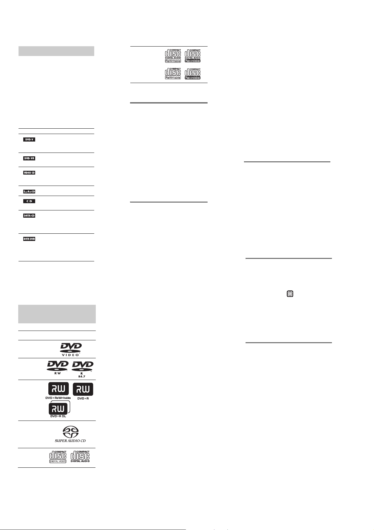
This System Can Play the
Following Discs
Format of
discs
DVD VIDEO
DVD-RW/
DVD-R
DVD+RW/
DVD+R
Super Audio
CD
(except for a
multi-channel
playback area)
VIDEO CD
(Ver. 1.1 and
2.0 discs)/
Audio CD
Disc logo
CD-RW/CD-R
(audio data)
(MP3 files)
(JPEG files)
“DVD+RW,” “DVD-RW,” “DVD+R,”
“DVD VIDEO,” and the “CD” logos are trademarks.
Note about CDs/DVDs
The system can play CD-R O M s / C D - R s /CDRWs recorded in the following formats:
–audio CD format
–video CD format
–MP3 audio tracks, JPEG image files, and
DivX video files* of format conforming to
ISO 9660 Level 1/Level 2, or its extended
format, Joliet
The system can play DVD-ROMs/DVD+RWs/
DVD-RWs/DVD+Rs/DVD-Rs recorded in the
following formats:
–MP3 audio tracks, JPEG image files and
DivX video files* of format conforming to
UDF (Universal Disc Format)
*European models only
Example of discs that the
system cannot play
The system cannot play the following discs:
•CD-ROMs/CD-Rs/CD-RWs other than those
recorded in the formats.
•CD-ROMs recorded in PHOTO CD format
•Data part of CD-Extras
• DVD Audios
• DATA DVDs that do not contain MP3 audio
tracks, JPEG image files, or DivX video files *
*European models only
• DVD-RAMs
Also, the system
discs:
•A DVD VIDEO
•A disc that has a non-standard shape (e.g.,
card, heart)
•A disc with paper or stickers on it
•A disc that has the adhesive of cellophane tape
or a sticker still left on it
cannot play the following
with a different region code
Notes about CD-R/CD-RW/DVD-R/
DVD-RW/DVD+R/DVD+RW
In some cases, CD-R/CD-RW/DVD-R/DVDRW/DVD+R/DVD+RW cannot be played on
this system due to the recording quality or
physical condition of the disc, or the
characteristics of the recording device and
authoring software.
The disc will not play if it has not been correctly
finalized. For more information, see the
operating instructions for the recording device.
Note that some playback functions may not
work with some DVD+Rs/DVD+RWs, even if
they have been correctly finalized. In this case,
view the disc by normal playback. Also some
DATA CDs/DATA DVDs created in Packet
Write format cannot be played.
Music discs encoded with
copyright protection
technologies
This product is designed to play back discs that
conform to the Compact Disc (CD) standard.
Recently, various music discs encoded with
copyright protection technologies are marketed
by some record companies. Please b e aware that
among those discs, there are some th at do n ot
conform to the CD standard and may not be
playable by this product.
Note on DualDisc
A DualDisc is a two sided disc product which
mates DVD recorded material on one side with
digital audio material on the other side.
However, since the au di o material side does no t
conform to the Compact Disc (CD) standard,
playback on this product is not guaranteed.
About Multi Session CD
•This system can play Multi Session CDs when
an MP3 audio track is contained in the first
session. Any subsequent MP3 audio tracks
recorded in later sessions can also be played
back.
•This system can play Multi Session CDs when
a JPEG image file is contain ed in the first
session. Any subsequent JPEG image files
recorded in later sessions can also be played
back.
•If audio tracks and images in music CD format
or video CD format are recorded in the first
session, only the first session will be played
back.
Region code
Your system has a region code printed on the
rear of the unit and will only play DVDs labeled
with the same region code.
DVD VIDEOs labeled will also play on this
ALL
system.
If you try to play any other DVD VIDEO, the
message [Playback prohibited by area
limitations.] will appear on the TV screen.
Depending on the DVD VIDEO, no regi on code
indication may be given even though playing the
DVD VIDEO is prohibited by area restrictions.
Note on playback operations
of DVDs and VIDEO CDs
Some playback operations of DVDs and VIDEO
CDs may be intentionally set by software
producers. Since this system plays DV Ds and
VIDEO CDs according to the disc contents the
software producers designed, some playback
features may not be available. Also, refer to the
instructions supplied with the DVDs or VIDEO
CDs.
6
Page 7
HCD-X1V
B
B
DMB12 board
(side A)
DMB12 board
(side B)
Please place a sheet
for insulation.
HOW TO IDENTIFY OPTICAL PICK-UP BLOCK
There are two kinds of OPTICAL PICK-UP BLOCK in this set.
When replacing the OPTICAL PICK-UP BLOCK, make sure which OPTICAL PICK-UP BLOCK it is following the “How to Identify” in
the figure shown below.
Printed of KHM-310CAB or KHM-313CAB.
KHM-310CA
or
KHM-313CA
DMB12 BOARD SERVICE POSITION
7
Page 8
HCD-X1V
t
POWER BOARD SERVICE POSITION
POWER board
Note
: The Power board can be removed individually.
Please place a shee
for insulation.
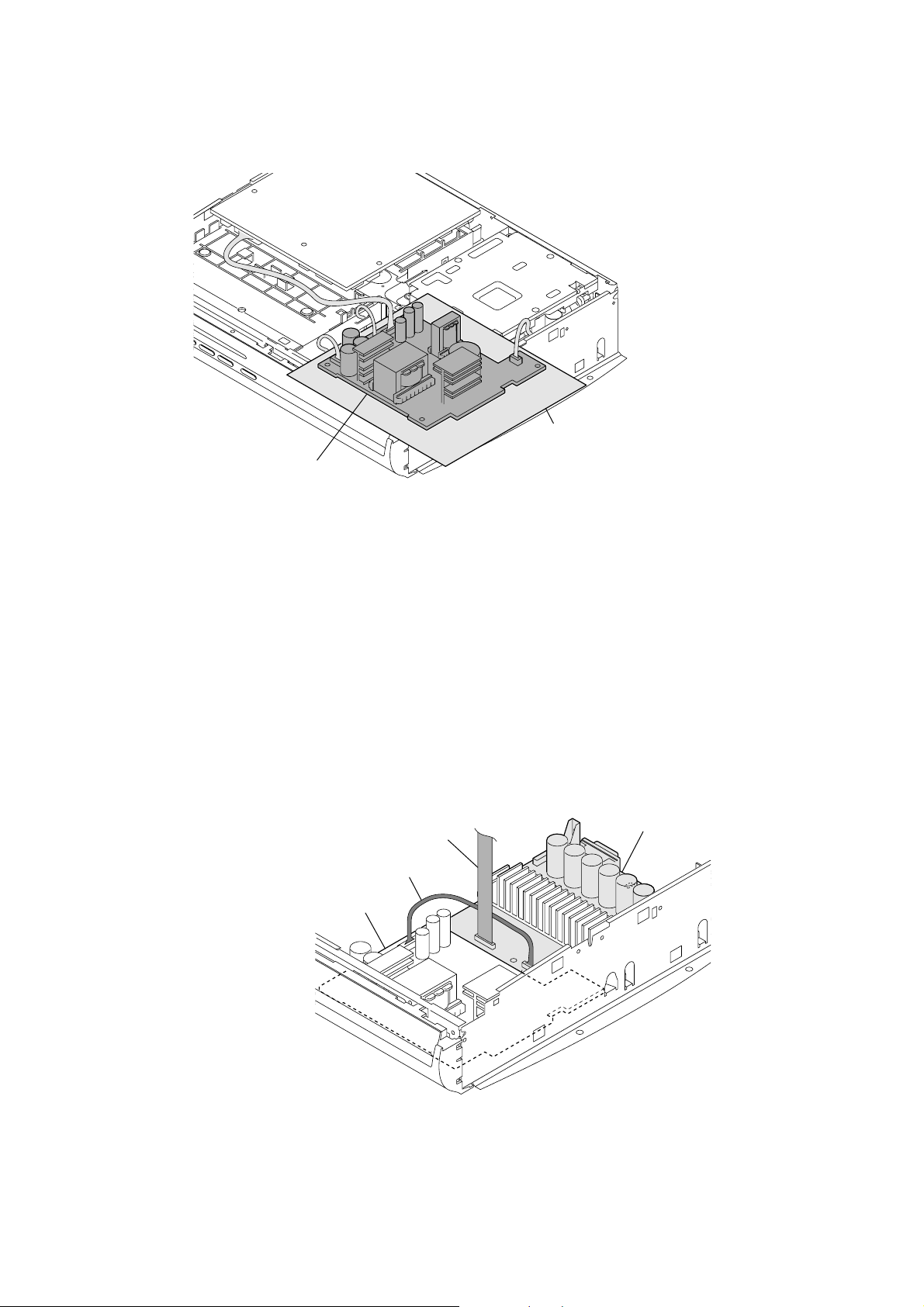
NOTE ON WIRE PROCESSING BETWEEN AMP BOARD AND POWER BOARD
Note
:To prevent a contact with the components on the primary side of power supply,
the wires should be routed in front of the wire (flat type) (19 core) and reshaped.
wire (flat type) (19 core)
wire
POWER board
AMP board
8
Page 9
MAIN BOARD SERVICE POSITION
AMP board
(component side)
AMP board
(conductor side)
Please place a sheet
for insulation.
1 wire (flat type) (9 core)
(US, Canadian models)
wire (flat type) (11 core)
(AEP, UK models)
(CN303)
HCD-X1V
3 Remove the Back Panel,
and then the MAIN board.
4
2 connector
(CN1000)
AMP BOARD SERVICE POSITION
Please place a sheet
for insulation.
MAIN board
9
Page 10
HCD-X1V
)
DVD MECHANISM DECK (CDM69EH) SERVICE POSITION
In checking the DVD mechanism deck (CDM69EH), prepare jig (extension cable J-2501-248-A: 1.00 mm Pitch, 27 cores, Length 300
mm).
DVD mechanism deck
(CDM69EH)
wire (flat type) (27 core)
MAIN board
(CN621)
connect jig (extension cable J-2501-248-A
to the MAIN board (CN621) and
wire (flat type) (27 core).
PRECAUTION WHEN INSTALLING A NEW OPTICAL PICK-UP BLOCK/
PRECAUTION BEFORE UNSOLDERING THE STATIC ELECTRICITY
PREVENTION SOLDER BRIDGE
CAUTION
When installing a new Optical Pick-up block, be sure to connect
the flexible printed circuit board first of all before removing the static
electricity prevention solder bridge by unsoldering. Remove the static
electricity prevention solder bridge by unsoldering after the flexible
printed circuit board has already been connected.
(Do not remove nor unsolder the solder bridge as long as the Optical Pick-up block is kept
standalone.)
flexible flat cable (24 core)
optical pick-up block
10
Page 11
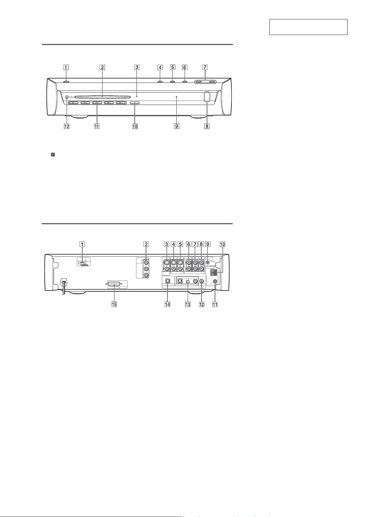
Front panel
SECTION 2
GENERAL
HCD-X1V
This section is extracted from
instruction manual.
A "/1 (on/standby)
B Disc slot
C (remote sensor)
D N (play)
E x (stop)
F FUNCTION
G VOLUME –/+
Rear panel
HDMI
OUT
SPEAKER
IMPEDANCE USE 4
A HDMI OUT jack
B COMPONENT VIDEO OUT jacks
C MONITOR OUT (S VIDEO/VIDEO) jacks
D VIDEO1 (VIDEO IN, S VIDEO/VIDEO)
jacks
E VIDEO2 (VIDEO IN, S VIDEO/VIDEO)
jacks
F VIDEO1 (AUDIO IN L/R) jacks
G VIDEO2 (AUDIO IN L/R) jacks
H TV (AUDIO IN L/R) jacks
H Front surround indicator
I Front panel display
J Z (eject)
K DISC 1-5/indicator
L AUDIO IN jack
VIDEO1
VIDEO2
COMPONENT
VIDEO
OUT
P
B/CB
PR/C
VIDEO2
VIDEO1
S VIDEOY
VIDEO
VIDEO INMONITOR
R
OUT
TV
DIGITAL IN
L
R
OPTICALOPTICAL
VIDEO1
AUDIO IN
COAXIAL COAXIAL
VIDEO2
TV
A.CAL
MIC
ECM-AC1
ANTENNA
AM
FM
75
COAXIAL
I A.CAL MIC jack
J AM terminal
K FM 75Ω COAXIAL jack
L VIDEO2 (DIGITAL IN COAXIAL) jack
M VIDEO1 (DIGITAL IN COAXIAL/
OPTICAL) jacks
N TV (DIGITAL IN OPTICAL) jack
O SPEAKER jacks
11
Page 12
HCD-X1V
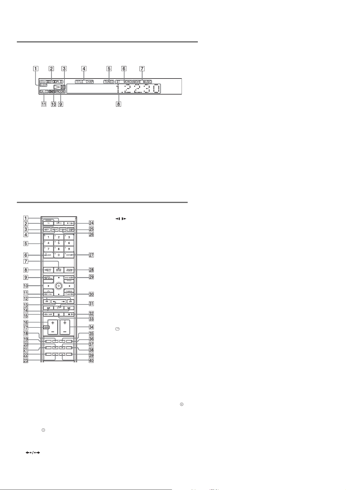
Front panel display
About the indications in the front panel display
A Lights up when the sleep timer is set.
B Current surround format (Except for
JPEG and Super Audio CD)
C Playing status (DVD function only)
D Lights up when the time information of
a title or chapter appears in the front
panel display. (DVD only)
E Lights up when a station is received.
(Radio only)
F Monaural/Stereo effect (Radio only)
G Lights up when the music or movie
mode is selected.
Remote control
With the cover opened.
A TV [/1 (on/standby)
B TV button/TV mode indicator
C SLEEP
D DISPLAY
E Number buttons
F CLEAR
3)
-/--
G MOVIE/MUSIC
H SOUND FIELD
I DVD TOP MENU
J C/X/x/c/
K O RETURN
L ./>
PRESET –/+
M (instant replay/instant
advance)
c/C STEP
3)
2)3)
H Displays system’s status such as
chapter, title, or track number, time
information, radio frequency, playing
status, sound field, etc.
I Lights up when the system outputs
progressive signals (DVD function
only).
J Lights up when the HDMI OUT jack is
correctly connected to HDCP (highbandwidth digital content protection)
compliant device with HDMI or DVI
(digital visual interface) input.
K Lights up when Super Audio CD/CD is
loaded.
N m/M
/
TUNING –/+
O DISC SKIP
P VOLUME +/–
TV VOL +/–
Q MUTING
R AUDIO
3)
2)
S PICTURE NAVI
T PROGRESSIVE
U DIMMER
V FM MODE
W DIRECT TUNING
X [/1 (on/standby)
Y THEATRE SYNC
Z TV/VIDEO
wj ENTER
1)3)
wk BASS/TREBLE
wl DVD MENU
e; DISPLAY
ea H (play)
TOOLS
TV MENU
3)
3)
2)
es x (stop)
ed X (pause)
ef FUNCTION +/–
TV CH +/–
2)
3)
eg SUBTITLE
eh ANGLE
ej SA-CD/CD
ek REPEAT
el AMP MENU
r; TUNER MENU
1)
The ENTER button is the same function as the
button.
2)
The H ea, 5 5, AUDIO qk, and FUNCTION +/
– ef buttons have tactile dots. Use the tactile dots as
references when operating the system.
3)
These buttons change to the TV operation buttons
when the remote is in TV mode. The remote is in TV
mode when the TV mode indicator 2 lights up by
pressing the TV button 2.
12
Page 13
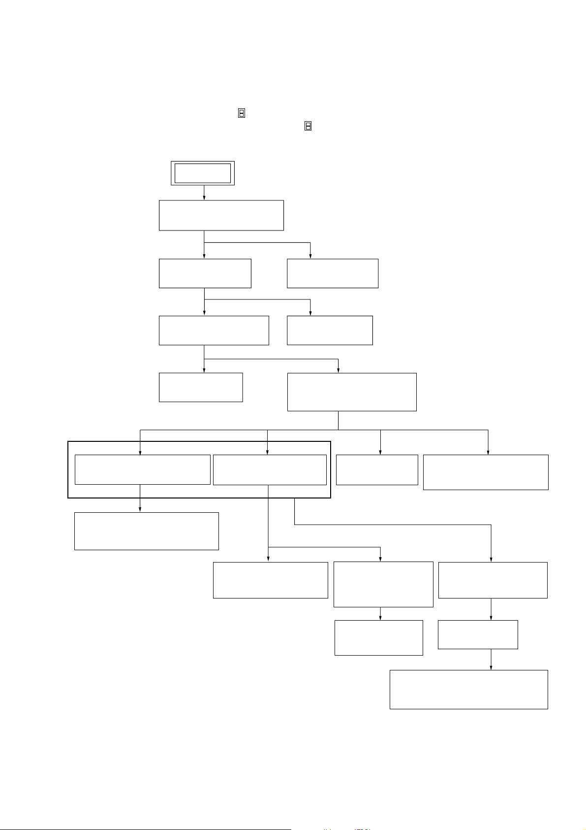
SECTION 3
3-7. MAIN BOARD
(Page 16)
SET
3-2. TOP PANEL, SIDE PANEL
(Page 14)
3-4. POWER BOARD
(Page 15)
3-3. DMB12 BOARD
(Page 14)
3-5. AMP BOARD
(Page 15)
3-8 . DVD MECHANISM DECK
(CDM69EH)
(Page 17)
3-9. OPTICAL PICK-UP SECTION
(Page 17)
3-10. OPTICAL PICK-UP BLOCK
(KHM-310CAB or KHM-313CAB)
(Page 18)
3-11. BRACKET (TOP) ASSY
(Page 18)
3-13. MOTOR (STOCKER)
ASSY (STOCKER) (M761)
(Page 19)
3-14. MOTOR (STOCKER)
ASSY (ROLLER) (M781)
(Page 20)
3-16. RUBBER ROLLER
(SLIDER) ASSY,
SUB CHASSIS
(Page 21)
3-17. TIMING BELT
(FRONT/REAR)
(Page 21)
3-12.RELAY BOARD
(Page 19)
3-15. MOTOR (STOCKER)
ASSY (MODE) (M771)
(Page 20)
3-18. CAM (GEAR)
(Page 22)
3-19. SENSOR BOARD,
ROTARY ENCODER (MODE) (S771)
(Page 22)
3-6. REAR PANEL BLOCK
(Page 16)
Note 1: The process described in can be performed in any order.
Note 2: Without completing the process described in , the next process can not be performed.
DISASSEMBLY
• This set can be disassembled in the order shown below.
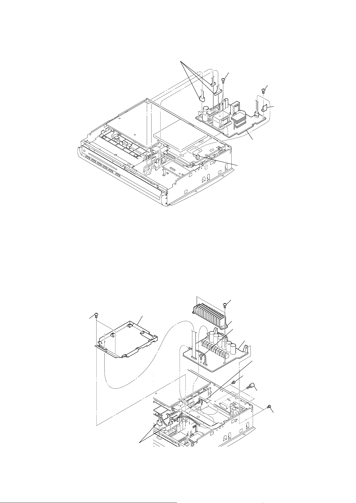
3-1. DISASSEMBLY FLOW
HCD-X1V
13
Page 14
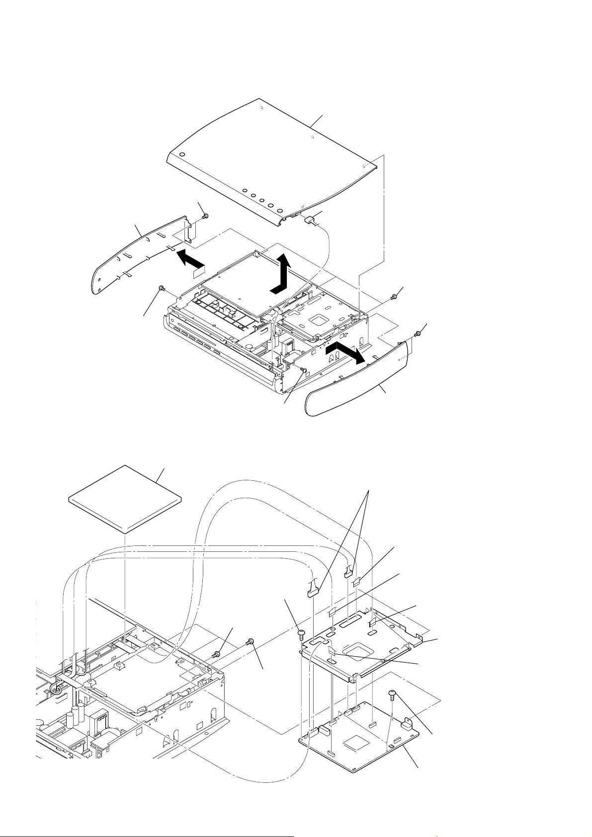
HCD-X1V
)
)
Note: Follow the disassembly procedure in the numerical order given.
3-2. TOP PANEL, SIDE PANEL
1
two screws
(BVTT3 × 8)
2
side panel (L)
6
screw
(BV/ring)
8
top panel
5
connector
(CN804)
7
three screws
(BV/ring)
3
two screws
(BVTT3 × 8
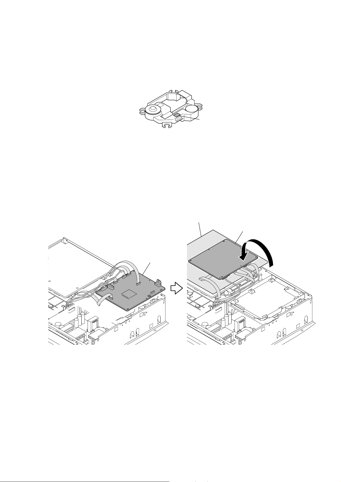
3-3. DMB12 BOARD
1
cushion (FFC)
6
8
8
screw
(BVTT3 × 6)
7
screw
(BV/ring)
four screws
(BVTT3 × 6)
three screws
(BV/ring)
4
side panel (R)
6
two connectors
(CN201, CN601)
2
wire (flat type) (11 core)
(CN4301)
3
wire (flat type) (24 core)
(CN101)
4
wire (flat type) (11 core)
(CN4501)
9
shield plate (DMB)
5
wire (flat type) (11 core
(CN109)
14
q;
8
three screws
(BVTT3 × 6)
DMB12 board
Page 15
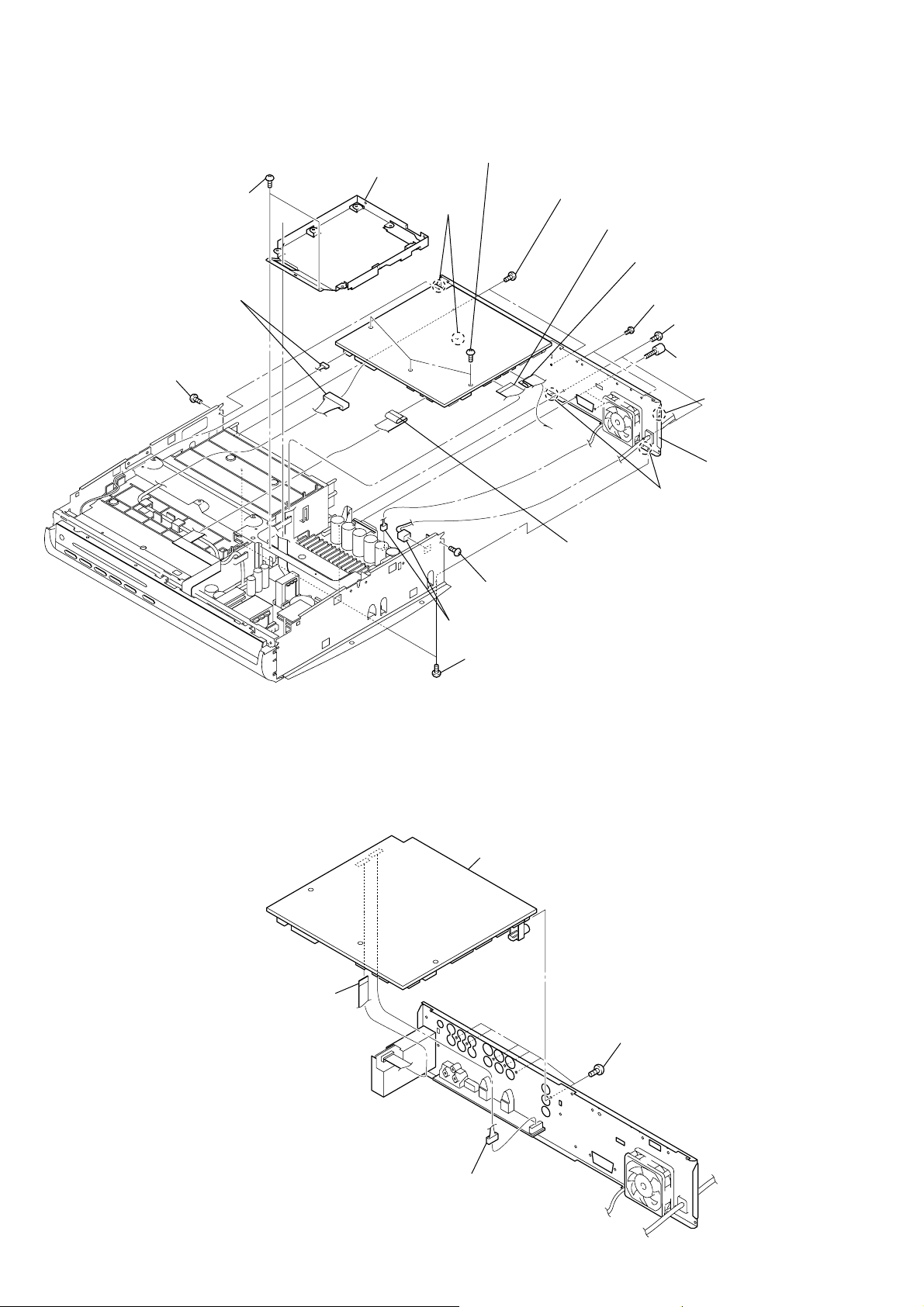
3-4. POWER BOARD
)
)
1
three connectors
(CN902, CN903,
CN904)
2
four screws
(BVTT3
1
×
6)
5
POWER board
connector
(CN905)
3
screws
(BVTT3
4
cover (L)
HCD-X1V
×
8
3-5. AMP BOARD
2
two screws
(BVTT3
×
6)
A
5
two connectors
(CN902, CN903)
4
bracket (DMB)
A
two screws
6
(BV3)
7
heart sink
8
screw (BV3)
qa
AMP board
1
wire (flat type) (19 core
(CN621)
3
two screws (BV/ring)
q;
two accessory screws
9
two screws
(BV/ring)
15
Page 16
HCD-X1V
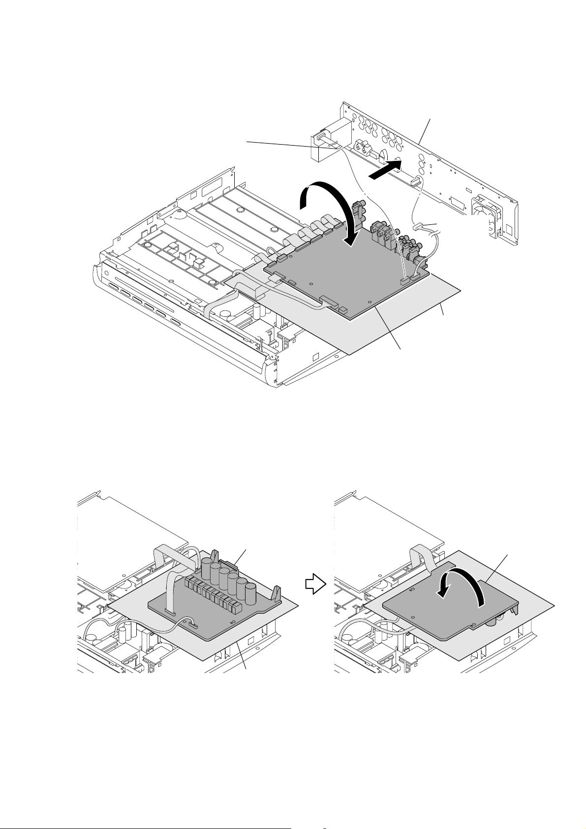
3-6. REAR PANEL BLOCK
5
9
4
two connectors
(CN401, CN506)
screw
(BVTT3
two screws
(BVTT3
×
6)
×
6)
A
7
bracket (DMB)
qd
two bosses
8
three screws
(BVTT3
×
6)
q;
A
two screws
(BV/ring)
2
wire (flat type) (27 core)
(CN621)
3
wire (flat type) (19 core)
(CN507)
6
two screws (BV/ring)
qs
two screws
(BV/ring)
qa
two accessory
screws
qd
boss
qf
back plate
block
qd
two bosses
3-7. MAIN BOARD
9
screw
(BVTT3
two connectors
4
(CN901, CN3000)
9
three screws
(BVTT3
4
MAIN board
1
wire (flat type) (19 core)
(CN501)
×
6)
×
6)
16
1
wire (flat type) (9 core)
(US, Canadian models)
wire (flat type) (11 core)
(AEP, UK models)
(CN303)
2
connector (CN1000)
3
six screws
(BV/ring)
Page 17
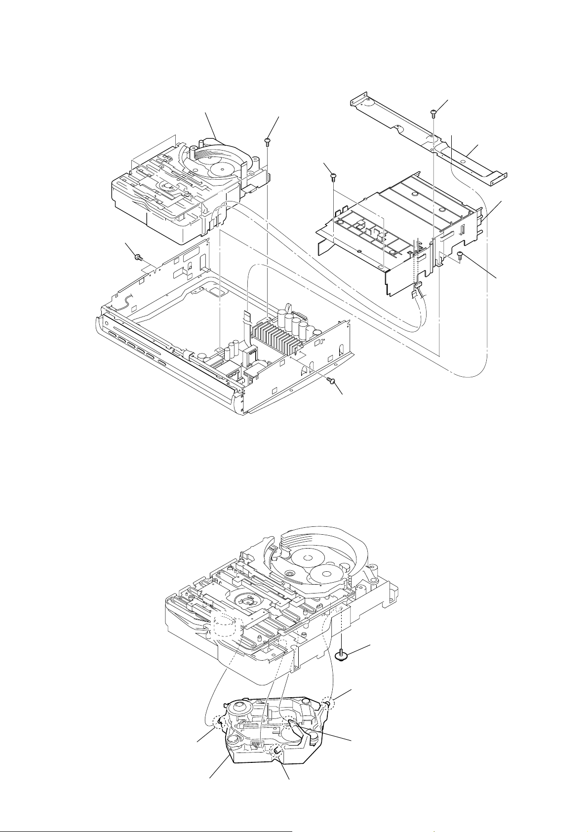
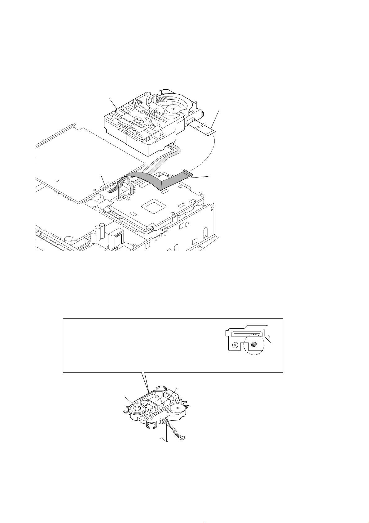
3-8. DVD MECHANISM DECK (CDM69EH)
)
7
DVD mechanism deck
(CDM69EH)
1
two screws
(BVTP3
×
8)
6
four screws
(BV3)
4
two screws
(BV3)
3
screw
(BVTT3
2
HCD-X1V
×
6)
bar
5
cover (CDM
4
screw
(BV3)
3-9. OPTICAL PICK-UP SECTION
1
two screws
(BVTP3
×
8)
1
floating screw (PTPWH M2.6)
3
boss
6
optical pick-up section
4
boss
2
5
boss
boss
17
Page 18
HCD-X1V
w
y
3-10. OPTICAL PICK-UP BLOCK (KHM-310CAB or KHM-313CAB)
2
5
optical pick-up block
(KHM-310CAB or
2
insulator screw
4
insulator
2
insulator screw
4
insulator
KHM-313CAB)
3
4
1
insulator screw
insulator
flexible flat cable (24 core)
2
insulator scre
4
insulator
3-11. BRACKET (TOP) ASSY
3
Lift up the
1
2
Lift up the
SW (1) board.
four
screws
(BTP2.6
SW (2) board.
×
6)
4
Lift up the
5
Lift up the
SW (3) board.
SW (4) board.
6
six screws
(BVTP2.6)
7
bracket (top) ass
18
Page 19
3-12. RELAY BOARD
CN705
– bottom view –
1
Remove thirteen solders of
CN704, CN705, CN706,
CN707, CN708.
CN704
CN707
4
connector
(CN703)
3
4
connector
(CN702)
4
connector
(CN710)
HCD-X1V
CN706
CN708
RELAY board
1
Remove five solders of
rotary encoder (stocker position) (S702).
3-13. MOTOR (STOCKER) ASSY (STOCKER) (M761)
3
5
stocker motor board
two screws
(BVTP2.6)
4
5
2
Remove two solders of
motor (stocker) assy (stocker) (M761)
2
Remove two solders of
6
motor (stocker) assy
(stocker) (M761)
2
RELAY board
.
connector (CN761)
four screws
(BVTP2.6)
.
1
belt (stocker)
19
Page 20
HCD-X1V
3-14. MOTOR (STOCKER) ASSY (ROLLER) (M781)
3
two screws
(BVTP2.6)
4
ROLLER MOTOR
5
motor (roller) assy
(roller) (M781)
board
2
Remove two solders of
motor (roller) assy (roller) (M781).
2
Remove two solders of
connector (CN781)
.
3-15. MOTOR (STOCKER) ASSY (MODE) (M771)
2
Remove seven solders of
connector (CN771).
MODE MOTOR board
2
Remove five solders of
rotary encoder (mode) (S771).
1
belt (roller V)
3
two screws
(BVTP2.6)
4
MODE MOTOR board
5
motor (stocker) assy
(mode) (M771)
20
2
Remove two solders of
motor (stocker) assy (mode) (M771).
1
belt (mode V)
Page 21
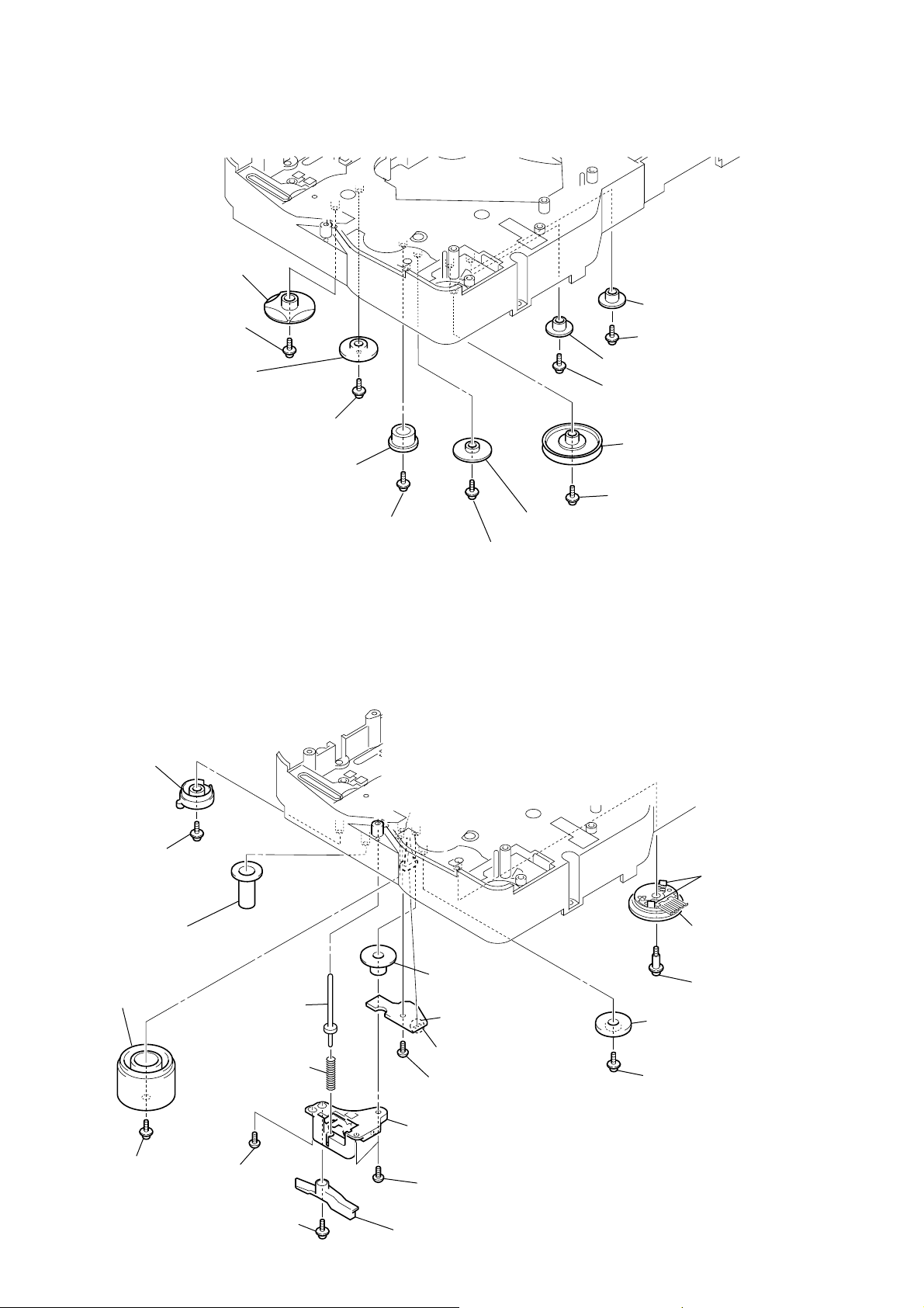
3-16. RUBBER ROLLER (SLIDER) ASSY, SUB CHASSIS
qg
sub chassis
qf
screw
(BVTP2.6
×
8)
8
step screw
qs
step screw
5
step screw
9
tension
spring
(slider 2)
6
tension spring
(slider 4)
0
rubber roller
(slider 4) assy
7
rubber roller
(slider 1) assy
qa
rubber roller
(slider 2) assy
qd
rubber roller
(slider 1) assy
3
tension spring
(base slider 5)
1
step screw
4
rubber roller
(slider 5) assy
2
rubber roller
(slider S) assy
bracket (top) assy
HCD-X1V
3-17. TIMING BELT (FRONT/REAR)
5
two gears
(center)
6
timing belt
(front)
4
gear
(timing)
3
slider (mode cam) assy
2
gear (mode cam)
Note: Refer to assembly (Section 4).
7
two gears (center)
8
timing belt (rear)
9
timing belt (rear)
When install three timing belts,
its pass under each claws.
timing belt
(rear)
claw
timing belt
(rear)
claw
timing belt (front)
claw
claw
1
screw
(PTPWH2.6
×
8)
21
Page 22
HCD-X1V
)
3-18. CAM (GEAR)
qf
Note: Refer to assembly
(Section 4: page 23).
qs
gear (mode cam)
Note: Refer to assembly
(Section 4: page 24).
cam (gear)
qd
screw
qa
screw
(PTPWH2.6
0
Note: Refer to assembly
(Section 4: page 24).
×
8)
gear (mode C)
9
screw
(PTPWH2.6
6
gear (mode 5)
5
screw (PTPWH2.6 × 8
4
gear (mode 5)
3
screw (PTPWH2.6 × 8)
2
pulley
(mode deceleration)
1
screw (PTPWH2.6 × 8)
8
gear (mode D)
×
8)
7
screw (PTPWH2.6 × 8)
3-19. SENSOR BOARD, ROTARY ENCODER (MODE) (S771)
Note: Refer to assembly
(Section 4: page 23).
qa
cam (eject lock)
q;
screw
qd
cam (BU U/D)
(PTPWH2.6
qf
gear (eject lock)
×
8)
6
shaft
(shutter)
5
compression spring
(shutter)
qg
gear (mode A)
7
Remove three solders
of
9
SENSOR board
8
screw
(BVTP2.6
connector (CN751)
×
8)
ql
two claws
w;
rotary encoder
(mode) (S771)
qk
screw
×
(PWH2
qj
.
gear (mode B)
qh
screw
(PTPWH2.6
6)
×
8)
qs
22
screw
(PTPWH2.6
4
base (shutter) block
3
8)
screw
(BVTP2.6
1
screw
(PTPWH2.6
×
8)
×
8)
3
two screws
(BVTP2.6
2
lever shutter (A)
×
8)
×
Page 23
SECTION 4
ASSEMBLY
• This set can be assembled in the order shown below.
4-1. HOW TO INSTALL THE CAM (EJECT LOCK)
1
Rotate the cam (BU U/D) fully in the direction of arrow.
2
Engage the gear (eject lock) and the gear of the cam (eject lock)
aligning the mark with the center of the gear (eject lock).
cam (BU U/D)
HCD-X1V
mark
gear (eject lock)
4-2. HOW TO INSTALL THE CAM (GEAR)
1
Check that the cam (BU U/D) can not be rotated in the direction of arrow.
2
Align the mark on the cam (gear) with the boss as shown in the figure
and install the cam (gear).
cam (gear)
cam (BU U/D)
cam (eject lock)
– bottom view • front –
boss
mark
– bottom view • front –
23
Page 24
HCD-X1V
4-3. HOW TO INSTALL THE GEAR (MODE C)
1
Align the mark on the rotary encoder (S771) with the projection of the assy.
2
Check that the cam (BU U/D) can not be rotated in the direction of arrow.
3
Install the gear (
rotary encoder
(S771)
mode
C).
gear (
mode
C)
cam (BU U/D)
mark projection
– bottom view • front –
4-4. HOW TO INSTALL THE GEAR (MODE CAM)
1
Slide the shaft in the direction of arrow.
2
Align mark A on the gear (mode cam) with mark B on the slider (mode cam) assy,
then install the gear (mode cam).
3
Check that mark C on the gear (mode cam) is in alignment with mark D on the cam (gear).
mark
A
gear (mode cam)
chassis
shaft
slider (mode cam) assy
24
cam (gear)
mark
D
– bottom view • front –
mark
mark
B
C
Page 25
HCD-X1V
2
five
solders
6
two gears
(stocker communication)
4
gear
(stocker communication)
RELAY board
ST ENCODER board
7
two screws
(PTPWH2.6
×
8)
5
screw
(PTPWH2.6
×
8)
3
screw
(PWH2
×
6)
rotary encoder
(S702)
gear
(stocker
communication)
– rear –
1
rotary encoder
(S702)
Engage the rotary encoder (S702)
and the gear (stocker communication)
as shown below in the figure.
2
two cams
(stocker U/D)
2
cam (stocker U/D)
3
two screws
(PTPWH2.6
×
8)
3
screw
(PTPWH2.6
×
8)
rotary encoder
(S702)
hole
gear
(stocker communication)
– rear –
screw
1
Position the hole on the gear
(stocker communication) on the
screw of the rotary encoder (S702).
To install three cams (stocker U/D), align each groove
of the cam (stocker U/D) with each
f
mark on the
chassis as shown in the figure.
f mark
f
mark
f
mark
cam (stocker U/D)
cam (stocker U/D)
cam (stocker U/D)
4-5. HOW TO INSTALL THE ROTARY ENCODER (S702), GEAR (STOCKER COMMUNICATION)
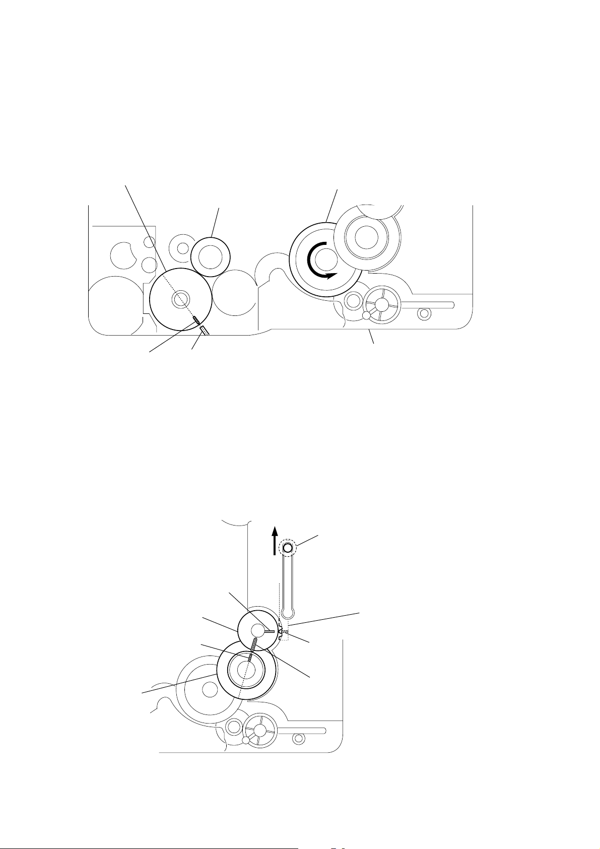
4-6. HOW TO INSTALL THE CAM (STOCKER U/D)
25
Page 26
HCD-X1V
4-7. HOW TO INSTALL THE STOCKER ASSY
1
Fit three shafts of the stocker assy in respective slits
of the cams (stocker U/D).
cam (stocker U/D)
cam (stocker U/D)
cam (stocker U/D)
Note:For the location of slits of the cams (stocker U/D),
see 4-6. HOW TO INSTALL CAM (STOCKER U/D).
cam (stocker U/D)
shaft shaftstocker assy
cam (stocker U/D)
shaft
26
pulley (stocker)
stocker assy
pulley (stocker)
A
2
Making sure that three shafts of the stocker assy fit in
respective slits of the cams (stocker U/D), rotate the
pulley (stocker) in the direction of arrow A by hand to
store the stocker assy.
Page 27
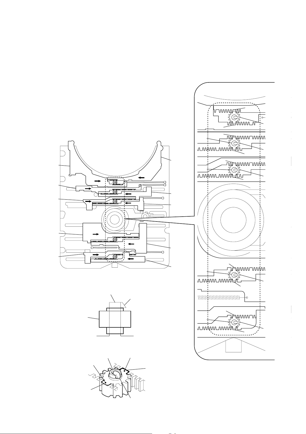
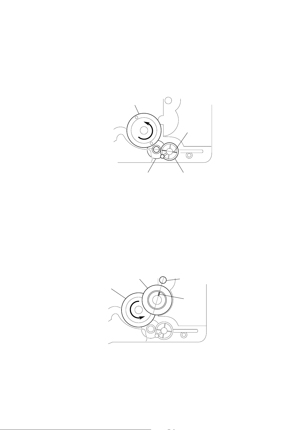
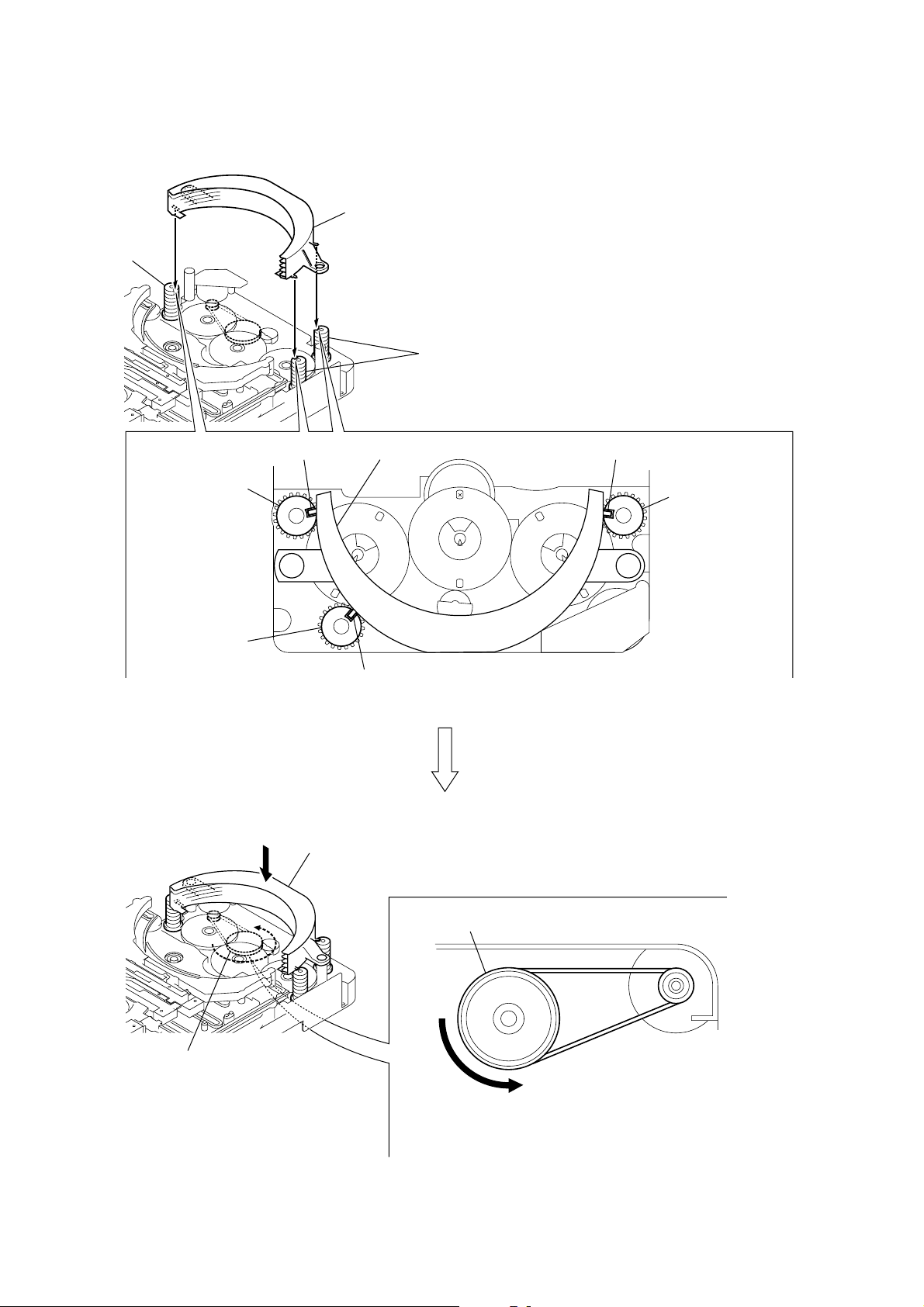
4-8. PHASE ADJUSTMENT BETWEEN PINIONS (SLIDER) AND SLIDER-1 TO 5 (L/R)
As shown in the following figure, adjust the portion A of each slider to the boss with the
1
slider-1 to 5 (L) and the slider-1 to 5 (R) pushed in the arrow directions respectively (see Fig. 1).
2
Paying attention to the up/down direction of the pinion (slider) (see Fig. 2), install each pinion (slider)
so that the portion
Note: Push in the pinion (slider) until the claw of the boss comes out above the pinion (slider) to lock.
B
of each pinion (slider) meshes with the portion A of each slider (see Fig. 3).
A
HCD-X1V
slider-5 (L)
slider-4 (L)
slider-3 (L)
slider-2 (L)
slider-1 (L)
(Fig. 1)
boss
claw
slider-5 (R)
slider-4 (R)
slider-3 (R)
slider-2 (R)
slider-1 (R)
boss
boss
boss
boss
A
A
A
A
A
A
pinion (slider)
pinion (slider)
A
pinion (slider)
pinion (slider)
pinion (slider)
pinion (slider) portion
slider portion
A
B
(Fig. 2)
boss
(Fig. 3)
pinion (slider) portion
slider portion
claw
A
boss
pinion (slider)
A
B
A
27
Page 28

HCD-X1V
SECTION 5
TEST MODE
AM STEP CHANGE (US and Canadian models)
The step interval of AM channels can be toggled between 9 kHz
and 10 kHz.
Procedure:
1. Press the I/1 button to turn on the system.
2. Press the [FUNCTION] button repeatedly to select the “TUNER
AM”.
3. Press the I/1 button to turn off the system.
4. Press two buttons of [FUNCTION] and I/1 simultaneously. The
system will turn on automatically. The message “AM 9k
STEP” or “AM10k STEP” appears on the fluorescent indicator
tube and thus the channel step is changed.
DVD VERSION VIEW
This mode is used to display the DVD version.
Procedure:
1. Press the I/1 button to turn on the system.
2. Press the [FUNCTION] button repeatedly to select the “DVD”.
3. Press the I/1 button to turn off the system.
4. Press two buttons of x and I/1 simultaneously. The system
will turn on automatically.
5. The DVD version appears on the TV screen.
COLD RESET
The cold reset clears all data including preset data stored in the
RAM to initial conditions.
Procedure:
1. Press the I/1 button to turn on the system.
2. Press three buttons of x , [FUNCTION] and I/1 simultaneously.
3. The message “COLD RESET” appears on the fluorescent
indicator tube, then becomes standby mode.
SHIP MODE
This mode moves the optical pick-up to the position durable to
vibration.
Procedure:
1. Press the I/1 button to turn on the system.
2. Press the [FUNCTION] button repeatedly to select the “DVD”.
3. Press three buttons of x , Z and I/1 simultaneously.
4. After the “ST ANDBY” blinking display finishes, the message
“MECHA LOCK” appears on the fluorescent indicator tube
and the ship mode is set.
PANEL TEST MODE
This mode is used to check the fluorescent indicator tube, LEDs,
keys, model, destination and software version.
Procedure:
1. Press three buttons of x , N and [DISC 3] simultaneously.
2. LEDs (amber) and all segments in fluorescent indicator tube
are lighted up. And half LEDs (green) and segments in
fluorescent indicator tube are lighted up, all LEDs and others
half segments in fluorescent indicator tube are lighted up, then
LEDs (amber) and all segments in fluorescent indicator tube
are lighted up. This operation is repeated.
3. Press the N button, the key check mode is activated.
4. In the key check mode, the fluorescent indicator tube displays
“K 0”. Each time a button is pressed, “K 0” value increases.
However , once a button has been pressed , it is no longer taken
into account.
5. When you want to enter the software version display mode,
press the [VOLUME +] button. The model information appears
on the fluorescent indicator tube.
6. Each time the [VOLUME +] button is pressed, the display
changes from destination information, MC version, GC
version, SYS version, DVD version, CDMA version, CDMB
version, ST version, TC version, TA version, DVD version,
TM version in this order, and returns to the model information
display.
7. When the [VOLUME --] button is pressed while the version
numbers are being displayed except model information and
destination information, the date of the software creation
appears. When the [VOLUME --] button is pressed again, the
display returns to the software version display. When the
[VOLUME +] button is pressed while the date of the software
creation is being displayed, the date of the software creation
is displayed in the same order of software version display.
8. To release from this mode, press three buttons in the same
manner as step 1 or disconnect the power cord.
AMP TEST MODE
Procedure:
1. Press three buttons of x , N and Z simultaneously. The
message “MEASURE” appears on the fluorescent indicator
tube.
2. Press the [SLEEP] button on the remote commander. The
message “SAFETY” appears on the fluorescent indicator tube.
3. Press the [SLEEP] button on the remote commander again.
The message “MEASURE” appears on the fluorescent
indicator tube.
4. Press the [SOUND FIELD] button on the remote commander.
The message “SWAP FULL” appears on the fluorescent
indicator tube.
5. Each time the [SOUND FIELD] button is pressed, the display
changes from SWAP THRU, SWAP F2S, SWAP F2CW in
this order, and returns to “SWAP FULL” .
6. Press the [BASS/TREBLE] button on the remote commander.
The message “D.C.A.C. MIC” appears on the fluorescent
indicator tube.
7. Press the [BASS/TREBLE] button on the remote commander
again. The message “FUNC INPUT” appears on the
fluorescent indicator tube.
8. Press two buttons of [VOLUME +] and [VOLUME --] simultaneously.
The message “VOL N” (volume normal operation) or “VOL
M/M” (volume MIN/MAX operation) appears on the
fluorescent indicator tube and thus the volume step is changed.
9. When the [VOLUME --] button is pressed in the volume MIN/
MAX operation state, the message “VOLUME MIN” appears
on the fluorescent indicator tube.
10. When the [VOLUME +] button is pressed in the volume MIN/
MAX operation state, the message “VOLUME MAX” appears
on the fluorescent indicator tube.
11. To release from this mode, press
COLD RESET.
I/1 button to execute the
PRODUCT OUT
This mode moves the optical pick-up to the position durable to
vibration and clears all data including preset data stored in the RAM
to initial conditions.
Procedure:
1. Press the I/1 button to turn on the system.
2. Press the [FUNCTION] button repeatedly to select the “DVD”.
3. Press three buttons of x , [DISC 3] and [VOLUME +]
simultaneously.
4. After the “STANDBY” blinking display f inishes, The message
“MECHA LOCK” appears on the fluorescent indicator tube
and the ship mode is set.
28
Page 29
HCD-X1V
DVD SECTION
1. DVD SER VICE MODE GENERAL DESCRIPTION
This mode let you make diagnosis and adjustment easily by using
the remote commander and the TV screen. The instructions,
diagnostic results, etc. are given on the on-screen display.
2. ENTERING DVD SERVICE MODE
Procedure:
1. Press the I/1 button to turn on the system.
2. Press the [FUNCTION] button repeatedly to select the “DVD”.
3. Press three buttons of x , Z and [VOLUME +] simultaneously .
4. The message “SERVICE IN” appears on the fluorescent
indicator tube and top menu of the Remocon Diagnosis Menu
appears on the on-screen display on the TV screen as follows.
The model name, IF-con version and Syscon version are
displayed at the bottom of the on-screen display.
Remocon Diagnosis Menu
0. External Chip Check
1. Servo Parameter Check
2. Drive Manual Operation
3. Emergency History
4. Version Information
Model Name :XZ1_xx
IF-con:Ver.xx.xx(xxxx)
Syscon:Ver.x.xxx
5. To execute each function, press its number by using numeric
button on the remote commander.
6. To release from this mode, press the
system.
I/1 button to turn off the
3. EXECUTING IOP MEASUREMENT
In order to execute IOP measurement, the following standard
procedures must be followed.
Procedure:
1. From the top menu of Remocon Diagnosis Menu, select “2
Drive Manual Operation” by pressing the [2] button on the
remote commander. The following screen appears on the onscreen display
Drive Manual Operation
1. Servo Control
2. Track/Layer Jump
3. Manual Adjustment
4. Mecha test mode
5. MIRR time Adjust
0. Return to Top Menu
Manual Adjust
1. Track Balance Adjust:
2. Track Gain Adjust:
3. Focus Balance Adjust:
4. Focus Gain Adjust:
5. Eq boost Adjust:
6. Iop:
7. TRV. Level:
8. S curve(FE) Level:
9. RFL(PI) Level:
0. MIRR Time:
V v Change Value
[RETURN]Return to previous menu
3. Select “6. Iop:” by pressing [6] button on the remote
commander.
4. Wait until a hexadecimal number appear in the on-screen
display as below.
Manual Adjust
1. Track Balance Adjust:
2. Track Gain Adjust:
3. Focus Balance Adjust:
4. Focus Gain Adjust:
5. Eq boost Adjust:
6. Iop: ED:
7. TRV. Level:
8. S curve(FE) Level:
9. RFL(PI) Level:
0. MIRR Time:
V v Change Value
[RETURN]Return to previous menu
5. Convert data from hexadecimal to decimal by using conversion
table.
6. If the value is smaller than 93 (decimal), then it is OK. Howev er
if the value is higher than 93, then BU (base unit) is defectiv e
and need to be change.
7. Press the
return to previous menu.
8. Press the [0] button on the remote commander to return to the
top menu of Remocon Diagnosis Menu.
9. Press the I/1 button to turn off the system.
O RETURN button on the remote commander to
4. CHECKING EMERGENCY HISTORY
To check the emergency history, please follow the following
procedure.
Procedure:
1. From the top menu of Remocon Diagnosis Menu, select “3.
Emergency History” by pressing the [3] button on the remote
commander. The following screen appears on the on-screen
display.
Emg. History Check
Laser Hours CD 999h 59min
DVD 999h 59min
2. Select “3. Manual Adjustment” by pressing the [3] button on
the remote commander. The following screen appears on the
on-screen display.
01. 01 05 04 04 00 92 46 00
00 00 00 00 00 00 23 45
02. 02 02 01 01 00 A9 4B 00
00 00 00 00 00 00 23 45
[Next]Next page [Prev]Prev page
[0]Return to Top Menu
29
Page 30
HCD-X1V
2. Y ou can check the total time when the laser is turned on during
playback of DVD and CD from the above menu. The maximum
time, which can be displayed are 999h 59min.
3. You can check the error code of latest 10 emergency history
from the above menu. To view the previous or next page of
emergency history, press the . or > button on the
remote commander. The er ror code consists of three kinds of
error codes.
A. Error code
Example of Error code
01. 01 05 04 04 00 92 46 00
00 00 00 00 00 00 23 45
The meaning of error code is as below:
01: Communication error (No reply from syscon)
02: Syscon hung up
03: Power OFF request when syscon hung up
19: Thermal shutdown
24: MoveSledHome error
25: Mechanical move error (5 changer)
26: Mechanical move stack error
30: DC motor adjustment error
31: DPD offset adjustment error
32: TE balance adjustment error
33. TE sensor adjustment error
34. TE loop gain adjustment error
35. FE loop gain adjustment error
36. Bad jitter after adjustment
40. Focus NG
42. Focus layer jump NG
51: Spindle stop error
52. Open kick spindle error
60: Focus on error
61: Seek fail error
62: Read Q data/ID error
70: Lead in data read fail
71: TOC read time out (CD)
80: Can’t buffering
81: Unknown media type
B. Parameter of error code
This is the detail of error code.
Example of Error code
To Clear the Laser Hour
Press the [ DISPLAY] button on the remote commander and then
press the [CLEAR] button on the remote commander. The data for
both CD and DVD data are reset.
Emg. History Check
Laser Hours CD 0h 0min
DVD 0h 0min
01. 01 05 04 04 00 92 46 00
00 00 00 00 00 00 23 45
02. 02 02 01 01 00 A9 4B 00
00 00 00 00 00 00 23 45
[Next]Next page [Prev]Prev page
[0]Return to Top Menu
To Clear the Emergency History
Press the [DVD TOP MENU] button on the remote commander and
then press the [CLEAR] button on the remote commander. The error
code for all emergency history would be reset.
Emg. History Check
Laser Hours CD 999h 59min
DVD 999h 59min
01. 00 00 00 00 00 00 00 00
00 00 00 00 00 00 00 00
02. 00 00 00 00 00 00 00 00
00 00 00 00 00 00 00 00
[Next]Next page [Prev]Prev page
[0]Return to Top Menu
To Execute the Initialize Setup Data
Procedure:
1. Press the [DVD MENU] button on the remote commander and
then press the [CLEAR] button on the remote commander . The
following screen appears on the on-screen display.
Emg. History Check
Laser Hours CD 999h 59min
DVD 999h 59min
01. 01 05 04 04 00 92 46 00
00 00 00 00 00 00 23 45
C. Time of error code
This is the laser time when an error occurred.
Example of Error code
01. 01 05 04 04 00 92 46 00
00 00 00 00 00 00 23 45
30
Initialize setup data...
[Next]Next page [Prev]Prev page
[0]Return to Top Menu
2. The screen after a while returns to former display.
To Return to the Top Menu of Remocon Diagnosis
Menu
Press the [0] button on the remote commander.
Page 31

e
VOLT/DIV: 200 mV
TIME/DIV: 500 ns
level:
0.58
±
1.23 Vp-p
(DVD-SL)
0.57 ± 1.1 Vp-p
(CD)
SECTION 6
ELECTRICAL CHECK
HCD-X1V
5. CHECKING VERSION INFORMATION
To check the version information, please follow the following
procedure.
Procedure:
1. From the top menu of Remocon Diagnosis Menu, select “4.
Version Information” by pressing the [4] button on the remote
commander. The following screen appears on the on-screen
display.
Version information
Firm(Main): Ver. X.XXXX
Firm(Sub): XX.XX
RISC: XXXXXX
8032: XXXXXX
Audio DSP: XX.XX.XX.XX
SubCPU: Ver.X.XX(XXXX)
[0]Return to Top Menu
2. To return to the top menu of Remocon Diagnosis Menu, press
the [0] on the remote commander.
DVD SECTION
RFMON LEVEL CHECK
Connection :
oscilloscop
DMB12 board
CN105 pin
CN105 pin
Procedure :
1. Connect an oscilloscope to CN105 pin 6 (RFMON) and
CN105 pin 3 (GND) on the DMB12 board.
2. Press the I/1 button to turn on the system.
3. Insert the test disc (DVD-SL (NTSC): HLX-503 (Part No. J6090-069-A, CD: YEDS-18 (Part No. 3-702-101-01) and press
the N button to playback.
4. Confirm that oscilloscope waveform is clear and check
RFMON signal level is correct or not.
Note: A clear RFMON signal waveform means that the shape “◊” can be
clearly distinguished at the center of the waveform.
6
(RFMON)
3
(GND)
+
–
Connecting Location:
– DMB12 Board (Side A) –
CN105
6
1
IC201
IC101
HCD-X1V
3131
Page 32

HCD-X1V
SECTION 7
DIAGRAMS
7-1. BLOCK DIAGRAM – RF SERVO/VIDEO Section –
6
DVDRFIP
MA
8
MB
9
MC
10
MD
11
DVDA2
DVDB3
DVDC4
DVDD5
TNI18VOE/E+G
TPI19VOF/F+H
V2O29VC
MDI120
MDI221
LDO123LD (780)
22LD (650)
LDO2
MSW
48VR (650)
LINYSW
136LIMIT
RF AMP, SERVO DSP,
MPEG DECODER
FOO42
TRO41
FMO38
DMO37
SPFG47
MUTE123MUTE12 184
MUTEMUTE34 183
TSD_MTSD-M 181
IOPMON40
RF+3.3V
OPTICAL PICK-UP
KHM-310CAB
KHM-313CAB
TX27M
A
(Page 33)
VOA/A
VOB/B
VOC/C
VOD/D
BLOCK
OR
MSW
VR (780)
FCS+
FCS– 37
TRK+ 35
TRK– 34
SL+ 29
SL– 30
SP+ 27
SP– 28
RF
PD
REGO2
REGO1
AUTOMATIC POWER
CONTROL (FOR CD)
Q102-1
AUTOMATIC POWER
CONTROL (FOR DVD)
Q102-2
IC201
FOCUS
COIL DRIVE
TRACKING
COIL DRIVE
SLED
SPINDLE
BUFFER
BUFFER
Q103
MUTE5
CD ON
SWITCH
Q101-1
DVD ON
SWITCH
Q101-2
FOCUS/TRACKING COIL DRIVE,
SPINDLE/SLED MOTOR DRIVE
36
MOTOR DRIVE
MOTOR DRIVE
46
47
41
31
REGULATOR
32
1
4
10
13
45
19
21
20
22
40
8
SPDIF 225
ASDATA0 217
ASDATA1 218
ASDATA2 219
ASDATA4 222
ABCK 214
ALRCK 213
ACLK 215
SMPTE_Y (0)
SMPTE_Y (1) 176
SMPTE_Y (2) 174
SMPTE_Y (3) 172
SMPTE_Y (4) 171
SMPTE_Y (5) 170
SMPTE_Y (6) 169
SMPTE_Y (7) 168
VCLK
SMBSY
VSYN
SMSDI
SMSDO
SMSCK
XSMCS
YUV3
YUV2
YUV1
IC101
YUV4
YUV5
YUV6
XTALI
229
177
178
207
205
209
210
208
211
198
196
194
200
202
203
2, 4, 5, 7, 8, 10, 11, 13, 42,
44, 45, 47, 48, 50, 51, 53
125 – 123, 121, 120, 118, 117,
115, 135, 133 – 128, 126
OSC BUFFER
IC111
YUV0
YUV1
YUV2
YUV3
YUV4
YUV5
YUV6
YUV7
VCLK
HSYNC
VSYNC
SMSDI
SMSDO
SMSCK
XSMCS
SPDIF
DQ0 – DQ15
RD0 – RD15
X101
27MHz
ASDATA0
ASDATA1
103
5
EEPROM
ABCK
ASDATA2
ASDATA4
147, 149 – 151, 166 – 164,
162, 160, 159, 146, 158
SDASDA
SCLSCL
EEWPWF
102
51
6
7
IC103
ALRCK
ACLK
SD-RAM
IC104
A0 – A11
23 – 26,
29 – 34, 22, 35
RA0 – RA11
HD0 – HD7
81 – 84,
86 – 88, 91
29, 31, 33, 35,
38, 40, 42, 44
DQ0 – DQ7
BUFFER
IC4501
BUFFER
IC4502
SPDIF
D1
D2
D3
BCK
LRCK
MCK
20
21
38
37
15
143
145
156
157
113
BA0 BA0
BA1 BA1
CKE CLKE
DQM0 LDQM
DRCLK CLK
HA0 – HA21
93, 78, 53 – 59, 75, 74,
72 – 67, 92, 60, 61, 76, 89
45, 25 – 18, 8 – 1,
48, 17, 16, 9, 10
A-1, A0 – A20
FLASH ROM
IC102
39
137
18
140
DQM1 UDQM
RAS RAS
(Page 34)
DIGITAL AUDIO BUS
HDMI BUS
B
C
(Page 33)
V1
VIDEO SELECTOR
IC202
V1
V2
C1
C2
Y1
Y2
17
19
16
1
VIN1
3
VIN2
5
VIN3
VIDEO SELECTOR
1
VIN1
3
VIN2
5
VIN3
VIDEO SELECTOR
1
VIN1
3
VIN2
5
VIN3
SW14SW2
2
IC201
SW14SW2
2
IC200
SW14SW2
2
VOUT
VOUT
VOUT
7
7
VIDEO AMP, 75Ω DRIVER
IC203
6
CVBSIN
4
CIN
7
8
YIN
11
SYIN
13
CBIN
15
CRIN
VOUTA
VOUTB
C OUT
S-DC OUT
YOUTA
YOUTB
CYOUTA
CYOUTB
CBOUTA
CBOUTB
CROUTA
CROUTB
MUTE114MUTE2
S1
5
2
Y1
C1
V2
Y2
C2
30
29
32
31
27
26
24
23
21
20
18
17
CY
CY
CY
• SIGNAL PATH
PB/C
PR/C
Y
B
R
VIDEO
S VIDEO
VIDEO
S VIDEO
VIDEO
S VIDEO
J200
COMPONENT
VIDEO OUT
J203
VIDEO2
J202
VIDEO1
J201
MONITOR
OUT
: CD PLAY
: DVD PLAY
139
142
138
CAS CAS
RCS CS
RWE WE
WIDE
179
: AUDIO
: VIDEO
: Y
: CHROMA
XROMCSCE
XRDOE
XWRWE
77
79
66
26
28
11
98
100
101
99
32
37
31
33
DVD_SID IFSOI
DVD_SCO IFSCK
DVD_SOD IFSDO
114
34
DVD XIFCS XIFCS
110
38
DVD_XIFBUSY XIF5SY
XRST
105
SWITCHING
SYSTEM CONTROLLER
MTK RST XSYSRST
IC150
IC501 (1/5)
56
V_SEL0
55
V_SEL1
54
V_SEL2
53
V_SEL3
: COMPONENT VIDEO
XRST
D
(Page 33)
HCD-X1V
3232
Page 33

7-2. BLOCK DIAGRAM – CHANGER/HDMI Section –
HCD-X1V
OFF:
In the midst disc is moving
S718
S717
between play position and
stocker
In the midst disc is moving
between play position and stocker
ON: disc is play position side,
OFF: disc is stocker side
OFF:
S716
The moment disc in/out
from stocker
OFF:
S715
When disc out from
play position
ON: Play position
S714
S713 (ON: Play position)
S711 (ON: When disc insert)
(8cm disc only)
M781
M
(ROLLER)
M771
M
(MODE)
M761
(STOCKER)
S718 (STOCKING)
S717 (DISC POSITION)
S716 (STOCKER IN/OUT)
S715 (DISC OUT)
S714 (DISC IN (8cm))
S713 (DISC IN (8/12cm))
S711 (DISC INSERT (8/12cm))
M
DISC INSERT
DETECT SENSOR
IC751
ROLLER MOTOR DRIVE
IC711
4
OUT1
OUT2
2 9
MODE MOTOR DRIVE
IC701
4
OUT1
OUT2
2 9
STOCKER MOTOR DRIVE
IC721
4
OUT1
OUT2
2 9
LEVEL SHIFT
Q731
CDM_OPEN_SW
35
IO_DI
IO_CLK
IO_CE
IO_RESET
87 DI126
89 CLK3
85 LATCH4
86
CHANGER CONTROLLER1
IC621
247
P0FIN
P1RIN 23
P2FIN 227
P3RIN 21
P4FIN 207
P5RIN 19
6
P14
P812
10
P10
9
P11
11
P9
8
P12
7
P13
2
RESET_B
LATCHO
DO2
DO1
CLKO
• SIGNAL PATH
: AUDIO
: VIDEO
HDMI TRANSMITTER
IC701
ASDATA0
ASDATA1
ASDATA2
ASDATA4
SPDIF
ACLK
ABCK
ALRCK
CHANGER CONTROLLER2
IC622
ROTARY
ENCODER
5 – 8
P15 – P12
9 – 12
P11 – P8
25
15
14
13
DI216
26
DI1
CLK3
LATCH4
RESET_B2
DO2
25
S771
(MODE)
ROTARY
ENCODER
S702
(STOCKER POSITION)
YUV0
YUV1
YUV2
YUV3
YUV4
YUV5
YUV6
YUV7
VCLK
HSYNC
VSYNC
EEPROM
IC706
AD076
75
AD1
AD2
74
AD3
73
SPDIF
72
ACL
77
ABCK
78
ALRCK
79
Y0
13
Y114
Y215
Y316
Y417
Y518
Y619
Y720
VCK11
HSYNC39
VSYNC
38
TCKN
HTPLG 40
CLK 26
52TX0P
51TX0N
55TX1P
54TX1N
58TX2P
57TX2N
49TCKP
48
LEVEL SHIFT
IC705
LEVEL SHIFT
Q701
LEVEL SHIFT
Q702
+5V
SW+9V
REGULATOR
IC707
CN701
HDMI OUT
7
9
4
6
1
3
10
12
19
16
15
18
TMDS DATA0 +
TMDS DATA0 –
TMDS DATA1 +
TMDS DATA1 –
TMDS DATA2 +
TMDS DATA2 –
TMDS CLOCK +
TMDS CLOCK –
HOT
SDA
SCL
+5V POWER
TX27M
A
(Page 32)
HCD-X1V
HDMI BUS
C
(Page 32)
IO-DO
SYSTEM CONTROLLER
IC501 (2/5)
88
SMSDI
SMSDI
SMSCK
XSMCS
VSYNC
31 SDO
30 SDI
32 SCK
23 XSMCS
22 VSYNC
SDA5SCL6WP
49
50
HDCP-SDA
7
51
HDCP-WP
HDCP-SCL
MSD
22
34
35
62
HDMI CONTROLLER
25
31
21
X701
10MHz
40
41
59
242761
63
X014X1
SCL0
SDA0
XTXRST
IC708
58
15
P35/AN05
XRST
21
XRST
D
RST
INTXTXINT
TRAP2TRAP2
SSCKSCK
SSOSDA
MSCK
(Page 32)
3333
Page 34

HCD-X1V
7-3. BLOCK DIAGRAM – AUDIO Section –
AUDIO IN
J401
A.CAL MIC
ECM-AC1
J801
AUDIO IN
(Page 32)
DIGITAL AUDIO BUS
B
FM 75Ω
COAXIAL
AM
VIDEO1
VIDEO2
ANTENNA
• R-ch is omitted due to same as L-ch.
• SIGNAL PATH
: AUDIO
: TUNER (FM/AM)
: DIGITAL AUDIO IN
: MIC INPUT
DSP
IC2
97 NOUAUDIO∗
82 DPSIE
78 DPSIA
41Y
72Y
124Y
A/B
70
SEL_SA-CD
6DSP_MISO
3DSP_INTR 15 INT_REQ
71DSP_SPIDS 122 SPIDS∗
72DSP_RESET 121 RESET∗
79 DPSIB
89 DPBCK
88 DPLRCK93Y
94 DPFSCK
80 DPSIC
81 DPSID
127 MOSI
125 SPICLK
16 DIR_ERR
126 MISO
CLKIN
142
(Page 35)
AMP BUS
64DPSOA
65DPSOB
70DPSOC
87DPDVBCK
86DPDVLRCK
D1
D2
D3
BCK
LRCK
MCK
DIR_XSTATE
E
F
(Page 35)
XTAL
143
R-CH
IC771
A/D CONVERTER
IC701
19 AINL
16 AINR
6 BCLK
3 LRCLK
1 MCLK
18
DIR_ZERO
2DOUT
ASDATA0
ABCK
ALRCK
ACLK
DATA SELECTOR
IC704
ASDATA1
ASDATA2
21A
31B
5
2A
62B
11
3A
10 3B
14
4A
1314B
AUDIO SELECTOR
J201
L
TV
R
L
R
L
R
R-CH
R-CH
R-CH
R-CH
R-CH
TUNER (FM/AM)
FM ANT
L-CH
R-CH
AM ANT
DIN
DO
CLK
CE
TUNED
RDS-DATA
RDS-CLOCK
MIC AMP
IC401
R-CH
(AEP, UK)
AUDIO SELECTOR
IC351
12 13X0 X
15 X2
14 X1
B
10A9
100 MIC/A.CAL SW
59 MIC_SW2
44 ST_DI
47 ST_DO
45 ST_CLK
48 ST_CE
43 TUNED
42 RDS_DATA
75 RDS_CLK
Q305
Q397
IC350
15 13X2 X
11 X3
14 X1
12 X0
10A9
B
Q396
Q395
50
MUTING
Q302
MUTING CONTROL
SWITCH
Q304
49
A_SEL2
A_SEL458A_SEL151A_SEL052A_SEL3
LINE AMP
R-CH
DIGITAL IN
IC360
TV
OPTICAL
VIDEO1
OPTICAL
VIDEO1
COAXIAL
VIDEO2
COAXIAL
OPTICAL
RECEIVER
IC1000
OPTICAL
RECEIVER
IC1001
J1000
WAVE
SHAPER
IC1003
DIGITAL AUDIO SELECTOR
IC1004
C
DIGITAL INPUT
13
XOUT
5Y
SW+3.3V
S1000
SELECTOR
OPTICAL
COAXIAL
2D2 4 DIN1 (I)
13 D6
15 D4
4D0
3D1
14 D5
11A10B9
X501
5MHz
15
XIN
SYSTEM CONTROLLER
IC501 (3/5)
DIGITAL AUDIO INTERFACE RECEIVER
3 DIN0 (I)
SPDIF
IC702
DO (O)DIR_HDOUT
DI (I)DSP_MOSI/DIR_DIN
CL (I)DSP_SPICLK/DIR_CLK
35 36
38
37
66
5
7
68
XOUT (O)
CE (I)DIR_HCE
CSFLAG (O)DIR_CSFLAG
25
34
19
27
ERROR (O)DIR_ERR
XIN (I)
XSTATE (O)DIR_XSTATE
XMODE (I)DIR_RST
17
48
67
69
24AUDIO (O)
16DATA (O)
14BCK (O)
15LRCK (O)
13CKOUT (O)
22
21
12.288MHz
SWITCHING
X701
HCD-X1V
X1
25MHz
3434
Page 35

7-4. BLOCK DIAGRAM – AMP Section –
HCD-X1V
(Page 34)
AMP BUS
E
DIR_XSTATE
F
(Page 34)
LRCK
D1
D2
D3
BCK
LRCK
MCK
Q701
D FLIP-FLOP
IC706
Q
4
CLK
2
SWITCHING
IC705
9
10
13
12
4
5
1
2
• SIGNAL PATH
: AUDIO
1
D
SW+
SW
SW+
SW
CN3500
SPEAKER
–
–
–
–
13
15
14
12
5
7
9
11
STREAM PROCESSOR
IC3010
DATA1
MCK1
BCK
LRCK
8
11
6
3
9
8
7
6
5
4
3
2
BUFFER
IC3500
SCDT
11
12
13
14
15
16
17
18
DATA1
DATA2
DATA3
BCK
LRCK
MCK2
MCK1
MCK3
SHIFT
LAT1
INIT
SOFTMUTE
OVF1
DATA3
MCK3
BCK
LRCK
SCDT
SHIFT
LAT3
INIT
SOFTMUTE
OVF2
31 11DATA
36 XFSIIN
30 BCK
29 LRCK
21 SCDT
22 SCSHIFT
23 SCLATCH
27 INIT
19 SOFTMUTE
24 OVFFLAGR
25 FLAGLOVF
STREAM PROCESSOR
IC3020
31 11DATA
36 XFSIIN
30 BCK
29 LRCK
21 SCDT
22 SCSHIFT
23 SCLATCH
27 INIT
19 SOFTMUTE
24 OVFFLAGR
OUTL1
OUTL1
9OUTL2
6OUTR1
4OUTR2
48XFSOIN
37FSOCKO
38FSOI
14XFSOOUT
48XFSOIN
38FSOI
14XFSOOUT
OSC BUFFER
IC3051
X3051
49.152MHz
9OUTL2
DIGITAL POWER AMP
IC3150
6 PWM_A OUT_A
14
14 PWM_B OUT_B
6
14 PWM_B OUT_B
6
14 PWM_B OUT_B
6
OUT_B
PWM_B
/SD
/RESET
5
4
DIGITAL POWER AMP
IC3100
PWM_A
OUT_A
/RESET4/SD
5
DIGITAL POWER AMP
IC3250
PWM_A
OUT_A
/RESET4/SD
5
DIGITAL POWER AMP
IC3200
OUT_A
PWM_A
/SD
/RESET
5
4
28 – 30
25 – 27
25 – 27
28 – 30
25 – 27
28 – 30
25 – 27
28 – 30
L.P.F.
L.P.F.
L.P.F.
L.P.F.
L.P.F.
L.P.F.
L.P.F.
L.P.F.
OVER LOAD
DETECT
Q3171, 3172
OVER LOAD
DETECT
Q3121, 3122
OVER LOAD
DETECT
Q3271, 3272
OVER LOAD
DETECT
Q3221, 3222
FRONT LCH+
FRONT LCH
FRONT RCH+
FRONT RCH
SYSTEM CONTROLLER
IC501 (4/5)
DAMP_SCDT
DAMP_SHIFT
DAMP LATCH1
DAMP LATCH2
DAMP LATCH3
DAMP INIT
DAMP SOFT MUTE
OVERFLOW1
OVERFLOW2
DRIVE_RST (EN)
DRIVE_OCP (DIAG)
1
2
78
79
80
76
77
83
84
81
82
SCDT
SHIFT
LAT1
LAT2
LAT3
INIT
SOFTMUTE
OVF1
OVF2
DATA2
MCK2
BCK
LRCK
SCDT
SHIFT
LAT2
INIT
SOFTMUTE
OVF1
STREAM PROCESSOR
IC3030
31 11DATA
36 XFSIIN
30 BCK
29 LRCK
21 SCDT
22 SCSHIFT
23 SCLATCH
27 INIT
19 SOFTMUTE
24 OVFFLAGR
25 FLAGLOVF
OUTL1
DIGITAL POWER AMP
IC3350
DRIVE
Q3000
D3351
REAR LCH+
REAR LCH
REAR RCH+
REAR RCH
4
–
2
1
–
3
M3000
M
(FAN)
OUT_B
OUT_A
/SD
4
28 – 30
25 – 27
25 – 27
28 – 30
L.P.F.
L.P.F.
L.P.F.
L.P.F.
OVER LOAD
DETECT
Q3371, 3372
OVER LOAD
DETECT
Q3301, 3302
M+13V
FAN MOTOR
Q3001, 3002
B+ SWITCH
(FOR FAN MOTOR)
6 PWM_A OUT_A
9OUTL2
6OUTR1
4OUTR2
48XFSOIN
38FSOI
PWM_B
14
/RESET4/SD
5
DIGITAL POWER AMP
IC3300
14 PWM_B OUT_B
6
PWM_A
/RESET
5
PROTECT DETECT
Q3351
HCD-X1V
3535
Page 36

HCD-X1V
7-5. BLOCK DIAGRAM – PANEL/POWER SUPPLY Section –
FL801
FLUORESCENT
INDICATOR
TUBE
D811
DISC 1
D812
DISC 2
D813
DISC 3
D814
DISC 4
D815
DISC 5
(AMBER)
(AMBER)
(AMBER)
(AMBER)
(AMBER)
D817
FOCUS
SUR
D818
WIDE
SUR
D819
2CH
STEREO
GRID DRIVE
(GRN)
(GRN)
(GRN)
(GRN)
(GRN)
Q802
FLUORESCENT INDICATOR
TUBE DRIVER
IC803
58OSC0
Q817
Q818
Q819
DAT
59OSC1
63
62CLK
61CS
60RST
3DATA
4CLK
5LCK
40 – 49 3 – 39
50
15
14
13
12
11
10
9
8
7
6
S1 – S35
AD1, AD2,
G1 – G10
G11
LED DRIVER
IC802
Q9
Q8
Q7
Q6
Q6
Q4
Q3
Q2
Q1
Q0
LED DRIVE
LED DRIVE
LED DRIVE
OSC
C809, R814
FL_D_OUT/LED_DATA
24
FL_CLK/LED_CLK
21
FL_CS/STB
25
FL_RESET
11
LED_LAT
22
PWM_OUT
SYSTEM CONTROLLER
IC501 (5/5)
LED1
23
LED2
28
LED3
36
P_CONT3
P_CONT2
A+9V
A+12V, M+12V
M+9V
T801
INVERTER
+3.3V
REGULATOR
IC105
+3.3V
REGULATOR
IC107
+3.3V
REGULATOR
IC703
+1.2V
REGULATOR
IC1
+1.8V
REGULATOR
IC110
+1.8V
REGULATOR
IC702
TRANSFORMER
VFL
PANEL+3.3V
SW+5V
RF+3.3V
HDMI+3.3V
LED+6V
A+5V
DSP+1.2V
SW+2.6V
SW+3.3V
HDMI+1.8V
FL
FL
RECT
D801,802,804, 805
FOR FLUORESCENT
INDICATOR TUBE
SERVO DSP+3.3V
41
26
40
SERVO DSPI+1.8V
+9V
REGULATOR
IC300
OSC
Q801
+3.3V
REGULATOR
IC502
RIPPLE
FILTER
Q504
+2.6V
REGULATOR
IC703
+3.3V
REGULATOR
IC505
+12V
REGULATOR
IC507
+9V
REGULATOR
IC507
+5V
REGULATOR
IC506
B+ SWITCH
(FOR LED)
Q501, 502
+5V
REGULATOR
IC504
M+13V
SHUNT
REGULATOR
IC951
RECT
D941
RECT
D944
RECT
D942
RECT
D943
T902
SUB POWER
TRANSFORMER
ISOLATOR
PC902
+32V
D922
RECT
D931
MAIN POWER
ON/OFF SWITCH
Q943
SHUNT
REGULATOR
IC931
RIPPLE FILTER
Q921
T901
MAIN POWER
TRANSFORMER
ISOLATOR
PC903
ISOLATOR
PC901
D905
D906, 907
D908
D935
POWER CONTROL
IC921
4 VCC
6 FB/OLP
8 STARTUP
1 DRAIN
TH901
RECT
D901
B+ SWICH
Q904
LINE FILTER
LF901
POWER CONTROL
IC901
1 OCP/SYNC
4 VCC
3D
5 FB/OLP
(AC IN)
F901
HCD-X1V
S801 – 812
(FRONT & TOP PANEL KEY)
REMOTE CONTROL
RECEIVER
IC801
4
SIRCS_IN
74
KEY INT
97, 95, 94
KEY0 – KEY2
P_CONT1
AC_CUT
RESET
AMP+1.8V
39
E+3.3V
20
12
RESET
SWITCH
Q503
SYSTEM+3.3V
RESET SIGNAL
GENERATOR
IC503
+1.8V
REGULATOR
IC3050
D502
D504
3636
Page 37

HCD-X1V
d
• Note for Printed Wiring Boards and Schematic Diagrams
Note on Printed Wiring Board:
• X : parts extracted from the component side.
• Y : parts extracted from the conductor side.
f
•
• : Pattern from the side which enables seeing.
(The other layers' patterns are not indicated.)
Caution:
Pattern face side: Parts on the pattern face side seen from
(Conductor Side) the pattern face are indicated.
Parts face side: Parts on the parts face side seen from
(Component Side) the parts face are indicated.
Caution:
Pattern face side: Parts on the pattern face side seen from
(Side B) the pattern face are indicated.
Parts face side: Parts on the parts face side seen from
(Side A) the parts face are indicated.
• DMB12 board is multi-layer printed board.
• Indication of transistor
: internal component.
However, the patterns of intermediate layers have not been
included in diagrams.
C
B
B
Q
E
Q
CE
These are omitted.
These are omitted.
Note on Schematic Diagram:
• All capacitors are in µF unless otherwise noted. (p: pF)
50 WV or less are not indicated except for electrolytics
and tantalums.
• All resistors are in Ω and 1/
specified.
f : internal component.
•
• 2 : nonflammable resistor.
• C : panel designation.
Note:
The components identified by mark 0 or dotted
line with mark 0 are critical for safety.
Replace only with part
number specified.
• A : B+ Line.
• B : B– Line.
• Voltages and waveforms are dc with respect to ground
under no-signal (detuned) conditions.
– DMB12 Board –
no mark : DVD PLAY
– Other Boards –
no mark : TUNER (FM/AM)
(): DVD PLAY
• Voltages are tak en with a V OM (Input impedance 10 MΩ).
Voltage variations may be noted due to normal production tolerances.
• Waveforms are taken with a oscilloscope.
Voltage variations may be noted due to normal production tolerances.
• Circled numbers refer to waveforms.
• Signal path.
J : CD PLAY
c : DVD PLAY
F : AUDIO
L : VIDEO
E : Y
a : CHROMA
r : COMPONENT VIDEO
f : TUNER (FM/AM)
i : DIGITAL AUDIO IN
N : MIC INPUT
4
W or less unless otherwise
Note:
Les composants identifiés par
une marque 0 sont critiques
pour la sécurité.
Ne les remplacer que par une
pièce portant le numéro
spécifié.
• Circuit Boards Location
POWER-SW board
AUDIO IN board
SW (2) board
SW (1) board
SENSOR board
MAIN board
LED board
SW (4) board
SW (3) board
TUNER (FM/AM)
KEY board
DISPLAY board
ROLLER MOTOR board
D-IO board
DMB12 board
AMP boar
LF board
POWER board
STOCKER MOTOR board
ST ENCODER board
RELAY board
HCD-X1V
MODE MOTOR board
3737
Page 38

HCD-X1V
• Semiconductor
Location
Ref. No. Location
IC101 E-4
IC102 E-2
IC103 F-2
IC104 G-4
IC110 C-5
IC201 C-3
IC701 G-8
IC708 F-7
Q101 B-5
Q103 B-5
7-6. PRINTED WIRING BOARD – DMB12 Board (Side A) –
1 2 3 4 5 6 7 8 9
A
DMB12 BOARD
B
C
R1173
CN109
1
D
2
R225
R223
R232
R230
R1143
R1145
(SIDE A)
R234
C233
C211
C209
CN201
FOR
C219
C221
CHECK
C222
25
C218
C224
36
IC201
112
R233
R231
37
R220
48
R212
C220
R226
R221
• See page 37 for Circuit Boards Location.
OPTICAL PICK-UP
BLOCK
KHM-310CAB
OR
KHM-313CAB
CN101
R1110
C118
C187
C101
1
3
CN105
24
C217
C119
13
C117
2D
2G
1S
R117
R116
IC110
Q101
R108
2S
1G
1D
E
Q103
2
: Uses unleaded solder.
C112
R111
C105
FB604
C602
(Page 51)
MAIN BOARD
B
CN601
C4501
CN505
C603
FL4501
R4520
FB605
FB606
R4501
1
2
R4701
R4805
R4502
(Page 50)
C
CN4301
R4703
R4702
MAIN BOARD
CN201
10
11
R4704
R4705
R4706
R4619
A
MAIN BOARD
CN504
(Page 50)
R1138
R1140
10
R1141
11
R1142
64
65
1
256
C150
IC102
E
C102
F
IC103
FB111
R193
R191
C177
FB106
R152
R153
C160
RB112
RB113
RB107
R1176
128
RB110
X101
C153
C152
IC101
R771
X701
16
17
32
33
R183
R185
R159
R162
193
129
RB111
RB103
RB109
RB108
RB104
RB115
R1114
RB114
RB116
RB117
R1183
R170
R140
192
R171
R1179
R1101
R166
R169
R167
R184
R160
R161
R163
R164
R165
C733
R790
R789
G
C1104
C1103
C190
FB108
IC104
11
10
R1715
R767
IC708
CN4501
48
1
2
R4803
R4802
R4801
FL705
C731
1
R763
R762
64
C702
1
49
C701
20
C736
R728
C707
60
LF701
LF702
LF703
LF704
41
C713
C715
FL703
C710
FL704
CN701
HDMI
OUT
FL701
C709
R793
80
61
IC701
21
C704
R1750
40
D
MAIN BOARD
CN701
(Page 50)
HCD-X1V
C179
C180
H
Note: When the DMB12 board is replaced by a repair for a fee, throw awa y the DMB12 board after
obtaining consent of not returning of the DMB12 board to the customer. When throwing a wa y
the DMB12 board, be sure to throw awa y after destroying EEPROM (IC103 and IC706) ph ysically with the hammer etc.
C197
1-868-160-
11
Note: EEPROM (IC103) cannot exchange with single. When EEPROM
3838
(IC103) is damaged, exchange the entire mounted board.
Page 39

HCD-X1V
7-7. PRINTED WIRING BOARD – DMB12 Board (Side B) – • See page 37 for Circuit Boards Location.
1 2 3 4 5 6 7 8 9
A
DMB12 BOARD
B
R5010
(SIDE B)
R4610
R4718
FL602
FB601
FB603
FL603
FB602
FL601
R118
R120
R121
R110
C106
R109
Q102
R1129
1C
1B
2E
R107
R114
C113
R123
R124
R115
R113
R112
1E
2B
2C
C
R4620
R5004
R5014
R5016
R748
R747
R749
R751
R752
(US, CND)
(AEP, UK)
R738
R742
C718
IC703
R730
C711
C712
C714
R750
R744
1
5
34
C725
IC705
R736
R734
R740
1
6
34
IC706
R745
R743
R725
R724
R723
R787
R722
C719
C716
46
13
C723
C720
R1706
C726
C703
R712
R718
R1705
IC702
C717
R1751
R788
D
E
F
G
R731
R709
R705
C730
R714
C729
R701
R708
R753
R4527
R4514
R704
R703
R702
IC707
IC4501
R4515
R4516
R772
G
R784
R756
C727
1346
R754
R4510
C732
Q701
R783
R4511
R759
R785
S
D
G
R4518
C4502
R765
IC4502
45
C4504
R4512
R4513
R760
R769
R773
R764
R781
R786
Q702
R766
13
R782
S
D
C734
R792
R1710
R778
R770
R780
IC107
FB112
R136
C135
C139
C143
R1125
R189
R779
C195
R1124
R190
45
R1168
R1167
R1102
R1120
R1121
R197
R1122
C132
C137
C141
C145
R142
FB123
R1123
13
R195
C192
C138
C142
C147
1
3
IC111
R192
C193
C130
C148
R1191
IC150
R1503
R1169
6
4
C161
R1185
C1105
C133
R172
R173
: Uses unleaded solder.
R102
C198
C183
R1178
R1134
C115
C124
C123
C122
C121
C120
C163
R175
R132
R1186
C157
C156
R174
R138
R1184
C140
C149
R126
1345
C154
C171
C1501
C151
R141
R146
C126
FB107
R143
C172
C1107
C1106
R133
R1502
R1501
C125
R101
C116
C174
C114
C199
C175
R130
R139
R135
C176
R1177
R1201
RB106
R224
C210
R219
C155
C158
C173
C181
C144
C127
C136
C162
C164
C213
R103
C128
R154
R145
R147
R1400
C191
R2504
R213
C208
R210
R204
R155
FB115
C131
R148
R1115
RB105
R216
C206
R205
C203
R207
R1133
R151
4
6
C186
IC105
R1152
R1151
R1150
C182
R156
R247
3
1
R246
R215
R209
C184
C215
R214
C214
C212
C205
R208
R105
R106
• Semiconductor
Location
Ref. No. Location
C105 D-8
IC107 D-5
IC111 E-5
IC150 G-6
IC702 E-3
IC703 F-2
IC705 G-2
IC706 F-2
IC707 G-3
IC4501 D-3
IC4502 D-4
Q102 B-5
Q701 G-4
Q702 G-4
R206
R1139
R1170
HCD-X1V
H
11
Note: When the DMB12 board is replaced by a repair for a fee, throw awa y the DMB12 board after
obtaining consent of not returning of the DMB12 board to the customer. When throwing a wa y
the DMB12 board, be sure to throw awa y after destroying EEPROM (IC103 and IC706) ph ysically with the hammer etc.
1-868-160-
Note: EEPROM (IC706) cannot exchange with single. When EEPROM
3939
(IC706) is damaged, exchange the entire mounted board.
Page 40

HCD-X1V
7-8. SCHEMATIC DIAGRAM – DMB12 Board (1/6) –
R102
0
C101
0.01
R1173
EEPROM
IC103
BR24L64F-WE2
0
XRST
(FOR CHECK)
(Page 52)
(Page 42)
(Page 45)
TRK-
TRK+
FCS-
FCS+
XRST
IOP
CN101
GND(LD)
LD(650)
N.C
N.C
PD
LD(780)
VR(650)
VR(780)
N.C
VOE/E+G
VCC
VC
VOF/F+H
VOB/B
VOA/A
RF
(LO:DVD.HI:CD)MSW
VOD/D
VOC/C
TRK-
TRK+
FCS+
FCS-
CN105
TXD
RXD
GND
SW+3.3V
V2REF0
RF MON
CN109
A1
A2
A3
24P
6P
11P
OCSW1/GND
XSYSRST
3.3V_MNT
XIFCS
XIFBSY
IFSDI
IFSDO
XAMUTE
IFSCK
DGND
N.C.
IOP
TRK-
TRK+
FCS-
FCS+
• See page 72 for Waveforms. • See page 74 for IC Block Diagrams.
(1/6)
R116
1k
DVD_LD
MSW
PD
CD_LD
VOE
V2O
VOF
VOB
VOA
RF
VOD
VOC
TRK-
TRK+
FCS+
FCS-
R101
100
TXD
RXD
V2REFO
R1110
2.7k
R1143
0
XSYSRST
R1145
0
R1138
0
R1139
R1140
R1141
R1170
R1142
1k
191
R
SDA
A
D
S
XIFCS
0
XIF5SY
0
IFSOI
0
IFSDO
0
XMAMUTE
0
IFSCK
2
D
A0
A
A1
N
G
O
L
F
C
VC
W
S
1k
R193
FB111
EEWP
SCL
Q101
UM6K1N-TN
IOP
LDO2
LDO1
DVD_LD
CD_LD
C184
0.01
FB108
XWR
Q101-1
CD ON SWITCH
Q101-2
DVD ON SWTICH
S
S-1
R113
22
R112
22
R109
0
R123
0
A16
A15
A14
A13
A12
A11
A10
A9
A20
A21
R105
10k
A19
R106
10k
A18
A8
A7
A6
A5
A4
A3
A2
A1
R117
47k
R1129
100k
FLASH ROM
IC102
Q103
RT1N241C-T112-1
INVERTER
-2-1
R114
100k
A16
BYTE
VSS
A-1
DQ7
DQ14
DQ6
DQ13
DQ5
DQ12
DQ4
VCC
DQ11
DQ3
DQ10
DQ2
DQ9
DQ1
DQ8
DQ0
OE
VSS
CE
A0
AUTOMATIC POWER
CONTROL (FOR CD)
-2
R111R108
1001M
C106
0.01
R115 R118 R120 R121
AUTOMATIC POWER
CONTROL (FOR DVD)
+3.3V REGULATOR
C105
22 22 22 22
TK11133CSCL-G
10V
R110
47k
Q102-2
IC105
NOISE
VOUT
GND
CONT
VIN
S29AL032D70TF-CHE2-0601UC(US,CND)
S29AL032D70TF-CHE2-0611CE(AEP,UK)
47
A15
A14
A13
A12
A11
A10
A9
A8
A19
A20
WE
RESET
N.C.
WP/ACC
RY/BY
A18
A17
A7
A6
A5
A4
A3
A2
A1
C192 C195 C193
0.01 0.22 0.22
R124R107
C112
47k10k
47
Q102
QST8TR
Q102-1
C113
0.01
R151
C182C186
0.220.22
10k
R1133
0
+3.3V REGULATOR
TK11133CSCL-G
C102
1
XROMCS
CONT
GND
NOISE
REGO1
+1.8V REGULATOR
IC110
MM1661JTRE
IC107
VIN
VOUT
SWITCHING
IC150
RA4
RA5
RA6
RA7
RA8
RA9
RA11
CLKE
DRCLK
RB108
RB107
0
0
TC7SZO8FU(TE85R)
G
C181
0.1
C191
0.1
R1501
R1503
0
R1502
0
0
DQM1
RD8
RD9
RD10
RD11
RD12
RD13
RD14
RD15
XRST1
XSYSRST
XRST
A17
A0
HD7
HD6
HD5
HD4
HD3
HD2
HD1
HD0
XRD
D
N
O
V
G
VIN
C187 R1178
C183C198
474V1k
0.331
FB106
FB112
V
SD-RAM
IC104
EDS6416AHTA-75-E
VSS
A4
A5
A6
A7
A8
A9
A11
NC
CLKE
CLK
UDQM
NC
VSS
DQ8
VDDQ
DQ9
DQ10
VSSQ
DQ11
DQ12
VDDQ
DQ13
DQ14
VSSQ
DQ15 DQ0
C190
47
10V
VSS
C179 C180 C197
0.1 0.1 0.1
LDQM
OSC BUFFER
IC111
TC7PAU04FU
(TE85R)
VDDGND
R1168
R1134
220
X101
27MHz
C1501
0.01
0
R1167
R142
0
100k
C152C153
15p15p
C157
0.01
FB123
SW+5V
RF+3.3V
SW+3.3V
REG02
SW+3.3V
SW+5V
GND
(Page
42)
(Page
R1169
47
R1186R1191
00
VDD
A3
A2
A1
A0
A10
BA1
BA0
CS
RAS
CAS
WE
VDD
DQ7
VSSQ
DQ6
DQ5
VDDQ
DQ4
DQ3
VSSQ
DQ2
DQ1
VDDQ
VDD
RA3
RA2
RA1
RA0
RA10
BA1
BA0
RCS
RAS
CAS
RWE
DQMO
RB106
47
RB105
47
VOD
VOC
VOB
VOA
VOE
VOF
EEWP
SDA
SCL
XRST1
XSYSRST
XIFCS
XIF5SY
RD7
IFSOI
RD6
IFSDO
RD5
XMAMUTE
RD4
IFSCK
LDO2
LDO1
RD3
V2REFO
RD2
TXD
RD1
RXD
RD0
PD
V2O
RF
MSW
A13
A12
A10
A11
A9
A7
A6
A4
A5
A8
TX27M
XTALI
VOD
VOC
VOB
VOA
VOE
VOF
EEWP
SDA
SCL
XRST
XSYSRST
XIFCS
XIF5SY
IFSOI
IFSDO
XMAMUTE
IFSCK
LDO2
LDO1
V2REFO
TXD
RXD
PD
V2O
RF
MSW
44)
(Page 41)
(Page
44)
(Page
41)
HCD-X1V
(Page 41)
Note: EEPROM (IC103) cannot exchange with single. When EEPROM
4040
(IC103) is damaged, exchange the entire mounted board.
Page 41

7-9. SCHEMATIC DIAGRAM – DMB12 Board (2/6) – • See page 72 for Waveforms. • See page 81 for IC Pin Function Description.
HCD-X1V
(Page
40)
(2/6)
CS
SDI
UTE
SCK
SDO
ACLK
XTALI
FB107
680k
R141
JITFO
XTALI
XTALO
RF AMP,SERVO DSP,MPEG DECODER
HA0
HA17
HD7
HD7
A0
A17
RFVDD18
DVSS
SPDIF
ASDATA4
0.01
C156
0.1
47
4.7k
47
C154
R143
R126
R146
GPIO
DVSS
SDPIF
SPDATA
DVDD18
ASDATA4
RFGND18
IC101
CXD9804R
IFSCK
IFSOI
IFSDO
XIFCS
DVDD18
URD
UWR
0.01
0
0
0
C155
R145
R147
R148
3.3k
3.3k
3.3k
R1152
R1151
R1150
IFSOI
XIFCS
IFSCK
IFSDO
VREFO
0.033
0.1
0.1
15k
0.1
C130
R136
C132
C133 C147 C148
0.1 0.047 0.047
OSP
OSN
IREF
RFGC
CEQN
AVDD3
VOA
VOB
VOC
VOD
RF
VOE
VOF
PD
LDO2
LDO1
V2REFO
V2O
VREFO
C116
DMO
FMO
IOPMON
TRO
FOO
C127
SPFG
MSW
EEWP
A2
A3
A4
A5
A6
A7
A8
A18
A19
R103
A1
A2
A3
C120
1
C121
1
C122
1
C123
1
C124
1
C125
0.1
C117
C118
C114
C115
0.11016V
0.11016V
C119
10
16V0.1
C126
0.1
C199
0.0047
0.01
R130
R135
0.01
10k
R1177
100
C128
0
0.0015
AGND
DVDA
DVDB
DVDC
DVDD
DVDRFIP
DVDRFIN
MA
MB
MC
MD
SA
SB
SC
SD
SDFON
SDFOP
TNI
TPI
MDI1
MDI2
LDO2
LDO1
SVDD3
CSO
RFLVL
SGND
V2REFO
V2O
VREFO
FEO
TEO
TEZISLV
OPOUT
OP_INN
OP_INP
DMO
FMO
TROPENPWM
IOPMON
TRO
FOO
USB_VSS
USBP
USBM
USB_VDD3
SPFG
MSW
CKSW
OCSW
EEWP
DVDD18
HA2
HA3
HA4
HA5
HA6
HA7
HA8
HA18
HA19
DVSS
APLLCAP
APLLVSS
HA13
HA15
HA14
HA16
XWR
APLLVDD3
2.2
C131
R
XW
A13
A14
A15
A16
22p
0.1
0.1
0.1
1
100k
R132
C135
C137
C139
0.001
C138
CEQP
HRFZC
RFGND
RFRPAC
CRTPLP
RFRPDC
HA20
HA9
HA10
DVDD3
HA11
HA12
0.01
C136
A9
A20
A11
A10
A12
0.1
C149
C140
C141
C143
C145
0.001
16V
10
C151
C150
IDAC
JITFN
LPFIP
LPFIN
LPFOP
LPFON
PLLVSS
PLLVDD3
ALE
HA21
HD6
HD5
HD4
HD3
DVSS
HD2
0
R1176
3
HD6
HD5
HD4
HD
HD2
A21
XROMCS
RFVDD3
XROMCS
0.1
C142
VSS
VCM
VDD3
VREFP
VREFN
HD1
HD0
DVDD3
XRO
HA1
0.01
C144
D
XR
HD1
HD0
A1
ASDATA2
47
R183
0
R152
SCL
ASDATA2
SCL
ASDATA1
47
R184
0
R153
SDA
ASDATA1
SDA
R1201
3.3k
R1400
ASDATA0
47
R185
ASDATA0
TRG-SW
ABCK
ALRCK
SM
VSYNC
HSYNC
XSM
SM
SM
XMAM
47
47
47
0.01
R163
R165
0
R162
0.01
C160
XSMCS
XSYSRST
XSYSRST
R167
0
0
0
R164
R166
R169
YUV7
VSYN
SMSDI
SMBSY
SMSCK
SMSDO
IR
R156
100
DVDD3
RD6
XIF5SY
DVSS
DQMO
RD7
XTXINT
0
R1115
RD6
RD7
DQMO
XIF5SY
R159
R160
R161
C161
DVSS
ACLK
ABCK
ALRCK
DVDD3
ICE
DVDD3
TXD
RXD
XRST
0
0
0.01
R154
R155
C158
XRST
RXD
TXD
V
Y
/B
CB
CR/R
150
R197
YUV6
YUV5
RD5
DVSS
RD4
RD5
C
Y/G
R1123 R1124R1122R1121R1120
R1125
R189R192R1102
150150150
150
150
R190
R195
0
0
R173
R172
YUV3
YUV2
YUV4
DAVSS
DAVSS
RD4
RB112
0
DAVDD
DAVDD
RD15
RD0
RD1
RD2
DVDD18
RD3
0.01
C162
RB113
0
D0
R
RD1
RD2
RD3
C163
0.01
YUV1
DAVSS
CIN
FS
DACVDDC
DAVCC
XDACS
ADSDO
FWD
REW
MUTE123
MUTE
DVDD3
TSD_M
ADSCK
WIDE
VCLK
SMPTE_Y(0)
SMPTE_Y(1)
DVSS
SMPTE_Y(2)
DVDD18
SMPTE_Y(3)
SMPTE_Y(4)
SMPTE_Y(5)
SMPTE_Y(6)
SMPTE_Y(7)
DVDD3
RA4
RA5
RA6
DVSS
RA7
DVSS
RA8
RA9
RA11
CKE
DRCLK
DVDD3
RCLKB
RVREF
DVDD18
RA3
RA2
RA1
DVSS
RA0
RA10
BA1
DVSS
BA0
RCS
DVDD3
RAS
CAS
RWE
DQM1
LINYSW
RD8
DVSS
RD9
RD10
RD11
RD12
RD13
RD14
DVDD3
0.01
C164
R1101
2.2k
R174
0
R175
0
C1103
R1179
100
R171
100
R1185
100
R1184
100
R140
10k
R170
10k
R138
100
R1183
220
R1114
22
R139
0
C173
0.001
FB115
0.001
C1104
0.001
C171
0.01
R133
0
C1107
0.001
C172
0.01
C174
0.01
C175
0.01
C176
0.01
10V
47
C177
0.001
C1105
C1106
0.001
RB116
47
RB117
47
0
RB114
0
RB115
0
RB104
0
RB103
0
RB111
RAS
CAS
RWE
DQM1
LIMITSW
RD8
0
RB109
RD9
RD10
RD11
RD12
0
RB110
RD13
RD14
RD15
RF
V2REFO
V2O
LDO2
LDO1
PD
XTALI
XMAMUTE
XIF5SY
XRST
SDA
XSYSRST
SCL
IFSOI
XIFCS
IFSCK
IFSDO
TXD
RXD
MSW
EEWP
VOA
VOB
VOC
MUTE123
VOD
MUTE
VOE
VOF
TSD_M
DMO
WIDE
FMO
VCLK
IOPMON
YUV0
TRO
YUV1
FOO
YUV2
SPFG
YUV3
VREFO
MUTE123
MUTE
YUV4
TSD_M
YUV5
LIMITSW
YUV6
YUV7
RA4
SPDIF
RA5
ASDATA2
RA6
ASDATA1
RA7
ASDATA0
ACLK
ABCK
RA8
ALRCK
RA9
CR/R
RA11
CB/B
CLKE
Y/G
V
DRCLK
C
Y
WIDE
RA3
SPDIF
RA2
ASDATA4
RA1
ASDATA2
RA0
ASDATA1
ASDATA0
RA10
ACLK
BA1
ABCK
BA0
ALRCK
RCS
HSYNC
VSYNC
VCLK
YUV0
YUV1
YUV2
YUV3
YUV4
YUV5
YUV6
YUV7
XSMCS
SMSDO
SMSDI
SMSCK
VSYNC
RF
V2REFO
V2O
LDO2
LDO1
PD
XTALI
XMAMUTE
XIF5SY
XRST
SDA
XSYSRST
SCL
IFSOI
XIFCS
IFSCK
IFSDO
TXD
RXD
MSW
EEWP
VOA
VOB
VOC
VOD
VOE
VOF
DMO
FMO
IOPMON
TRO
FOO
SPFG
VREFO
MUTE123
MUTE
TSD_M
LIMITSW
SPDIF
ASDATA2
ASDATA1
ASDATA0
ACLK
ABCK
ALRCK
CR/R
CB/B
Y/G
V
C
Y
WIDE
SPDIF
ASDATA4
ASDATA2
ASDATA1
ASDATA0
ACLK
ABCK
ALRCK
HSYNC
VSYNC
VCLK
YUV0
YUV1
YUV2
YUV3
YUV4
YUV5
YUV6
YUV7
XSMCS
SMSDO
SMSDI
SMSCK
VSYNC
GND
A4
A5
A6
A7
A8
A9
A10
A11
A12
A13
(Page 40)
(Page 42)
(Page 43)
(Page 44)
(Page 45)
(Page 40)
HCD-X1V
4141
Page 42

HCD-X1V
7-10. SCHEMATIC DIAGRAM – DMB12 Board (3/6) –
(3/6)
R221
C209
56k
0.033
C233
VREFO
SPFG
FOO
TRO
FMO
R208
R209
R204
1.2k
R210
R213
6.8k
C205
220p
33k
R206
10k
C206
220p
33k
R207
2.7k
R205
10k
C208
47k
0.01
FOCUS/TRACKING COIL DRIVE,
SPINDLE/SLED MOTOR DRIVE
R214
15k
R215
12k
C203
0.01
R216
12k
0.0047
R220
1k
R226
56k
R223
100k
C211
0.033
C214
0.001
C212
0.01
R230R212
82k10k
IC201
FAN8036L
R225
100k
R231
15k
IOP
IOPMON
R246
4.7k
RF+3.3V
SW+5V
SW+3.3V
REGO1
REG02
(Page 40)
R232
18k
R234
10k
33k
R233
C220
10
16V
C224
0.01
C219
0.01
C218
10
16V
C221
0.1
C222
0.1
C215
0.01
FCS-
TRK+
R247
FCS+
TRK-
FCS-
FCS+
TRK+
TRK-
IOP
VREFO
SPFG
FOO
TRO
FMO
DMO
MUTE123
MUTE
TSD_M
IOPMON
1k
SL-
SL+
SP-
SP-
SP+
SP+
SL-
SL+
SP-
SP+
LIMIT
(GND) LIMIT
SL-
SL+
CN201
SW+5V
SW+3.3V
GND
SW+9V
MTR_GND
(Page 43)
FCS-
FCS+
TRK+
TRK-
IOP
(Page 40)
VREFO
SPFG
FOO
TRO
FMO
DMO
MUTE123
MUTE
TSD_M
IOPMON
LIMITSW
6P
(Page 41)
HCD-X1V
MUTE123
DMO
R219
27k
R224
C210
0.01
C217
47
16V
R2504
4.7k
10k
C213
0.01
MUTE
TSD_M
4242
Page 43

7-11. SCHEMATIC DIAGRAM – DMB12 Board (4/6) –
MTR_GND
SW+9V
SW+3.3V
(Page 42)
GND
SW+5V
(4/6)
FB604
C602
10V
HCD-X1V
CN601
5P
FB605
FL602
C603
47
FB606
10V
47
FL603
FB601
FB603
FB602
MGND
SW+9V
SW+3.3V
DGND
SW+5V
(Page 52)
(Page 45)
(Page 41)
SW+9V
SW+3.3V
SPDIF
ASDATA0
ASDATA1
ASDATA2
ALRCK
CR/R
WIDE
CB/B
ABCK
ACLK
FL601
Y/G
Y
C
V
IC4501
SN74LVC541
GND
VCC
R4803
0
R4801 R4805
00
R4501
R4802
0
BUFFER
R4527
0
R4502
0
R4518
0
0
FL4501
C4504
0.01
C4501
R4610 R4619 R4620
0
0
0
0
0
0
0
100
100
100
100
100
0
000
CR/R
WIDE
CB/B
V-GND
CY/G
V-GND
Y
V-GND
C
V-GND
CVBS
D-GND
D1
D2
D3
BCKO
LRCKO
D-GND
MCKO
D-GND
SPDIF
D-GND
CN4301
11P
CN4501
11P
(Page 57)
(Page 54)
R4514
R4515
R4516
R4510
R4511
R4513
R4512
C4502
R4701
R4702
R4703
R4704
R4705
R4706
R4718
0.01
10
HCD-X1V
R4520
R5016
0
(AEP,UK)
BUFFER
IC4502
TC7SZ125FU
(TE85R)
0
GND
VCC
R5014
R5010
R5004
0
(US,CND)
0
0
4343
Page 44

HCD-X1V
7-12. SCHEMATIC DIAGRAM – DMB12 Board (5/6) –
(5/6)
ASDATA4
ASDATA2
ASDATA1
ASDATA0
ALRCK
ABCK
ACLK
SPDIF
R701
C701
0.1
0
C704
0.1
(Page 41)
ASDATA4
ASDATA2
ASDATA1
ASDATA0
ALRCK
ABCK
ACLK
SPDIF
VCLK
YUV0
YUV1
YUV2
YUV3
YUV4
YUV5
YUV6
YUV7
HSYNC
• See page 74 for IC Block Diagrams. • See page 81 for IC Pin Function Description.
C717
0.01
R734
0
R736
0
+1.8V REGULATOR +3.3V REGULATOR
C736
47
0
FS
VSYNC
SWING
VREF
DAC_AVDD3
AVDD3
AVDD3
PLL_AVDD3
PLL_AVDD3
HSYNC
HTPLG
4V
R1705
AVSS
TX2P
TX2N
TX1P
TX1N
AVDD
TX0P
TX0N
TCKP
TCKN
AVSS
AVSS
PLLC1
PLLC0
AVSS
AVSS
MSD
0.1
C709
DAC_AVDD3
TYPE
10k
R1750
R731
AVSS
ASDATA4
GND
CONT
NOISE
VIN
VOUT
C716 C719 C720
0.22 0.22 0.22
1k
0.0056
GATE SWITCH
IC705
TC7SZ08FU
(TE85R)
G
V
R730
C711
C712
FL701
C707
C714
22
10V
510
0.1
0.1
0.1
HDMI TRANSMITTER
DVSS
C0
C1
C2
C3
C4
C5
C6
C7
DVDD33
VCK
DVSS
Y0
Y1
Y2
Y3
Y4
Y5
Y6
Y7
0.1
C702
1k
R708
DVDD18
SSCK
ALRCK
0
R702
1k
R709
ALRCK
SSO
ABCK
0
R703
ACLK
0
R704
ABCK
DVDD18
4.7k
R705
ACL
PWDN
ASDATA0
AD0
RST
100
R712
ASDATA1
AD1
CLK
0
R788
ASDATA2
0
R793
AD2
INT
0.01
C703
ASDATA4
0
R714
AD3
DVSS
SPDIF
SPDIF
CXD9873Q
A7
R718
4.7k
IC701
R728
0
G
R
B
AVSS
DAC_AVDD3
MSCK
TRAP0
TRAP1
A6
TRAP2
10k
10k
0
0
R722
R723
R724
R725
SW+3.3V
SW+5V
GND
C718
0.01
R740
0
(Page 40)
IC703IC702
TK11133CSCL-GTK11118CSCL-G
R1706
1k
FL703
C710
10
16V
FL704
C715C713
47
10V
R744
4.7k
C725
R742
47k
0.01 0.1
R738
GND
CONT
NOISE
VOUT
VIN
C723
0.22
0
CN701
19P
HDMI
OUT
B1
B2
B3
C726
R743
LF701
LF702
LF703
LF704
R787
4.7k
R747
R748
R749
1.8k
R750
1.8k
0
R751
0
0
R752
0
EEPROM
IC706
BR24L16F-WE2
A0
A2
A1
GND
SDA
SCL
WP
VCC
1k
R745
1k
TMDS DATA2 +
TMDS DATA2 SHIELD
TMDS DATA2 -
TMDS DATA1 +
TMDS DATA1 SHIELD
TMDS DATA1 -
TMDS DATA0 +
TMDS DATA0 SHIELD
TMDS DATA0 -
TMDS CLOCK +
TMDS CLOCK SHIELD
TMDS CLOCK -
CEC
RESERVED
SCL
SDA
DOC/CEC GND
+5V POWER
HPD
HCD-X1V
(Page 40)
VSYNC
TX27M
R1751
10k
B4
B5
B6
B7
B8
(Page 45)
B9
B10
B11
Note: EEPROM (IC706) cannot exchange with single. When EEPROM
4444
(IC706) is damaged, exchange the entire mounted board.
Page 45

HCD-X1V
7-13. SCHEMATIC DIAGRAM – DMB12 Board (6/6) –
C732
0.01
X701
10MHz
R767
R766
4.7k
R765
0
0
• See page 72 for Waveforms. • See page 74 for IC Block Diagrams. • See page 81 for IC Pin Function Description.
(6/6)
0
HDMI CONTROLLER
AVCC
AVR
PE3/
INT13
PE2/INT12
PE1/INT11
PE0/INT10
P83
P82
P81
P80
P71/TI0
P70/TO0
MOD
X0
X1
VSS
AVSS
VDD
R763
0
R762
SCK
)
0/(CIN
PG
SDA
2/X1A
PG
AP2
TR
PG2/X0A
0
R772
N
ST
D
XPW
XTXR
MB95F108ASPFV-
VSYNC
XRST
06
P35/AN05
P36/AN
IC708
GE1-H0601
CS
XSM
XTXINT
08
07
P40/AN
P37/AN
P04/INT04
P03/INT03
N10
42/A
P41/AN09
P
T06
P05/INT05
P06/IN
P
CP-W
P43/AN11
HD
T07
I
P07/IN
SD
A
DCP-SD
H
PPG11/
PPG10/
TRG1/P53
PPG1/P52
TO01/P23
TO00/P22
PPG01/P21
PPG00/P20
PPG0/P14
O
SD
EC1/
DCP-SCL
H
T011/
T010/
SDA0
SCL0
EC0/P24
ADTG/
TRG0/
CK
S
Q701
2SK1399-T1B
P64
P63
P62
P61
P60
R785
0
10k
R781
10k
R782
C727
R786
0.01
0
R792
P13
4.7k
LEVEL SHIFT
Q702
2SK1399-T1B
LEVEL SHIFT
S
R754
0
T
D
ISE
GN
T
NO
VOU
CON
+5V REGULATOR
TK11150CSCL-G
VIN
IC707
B11
B10
B7
B8
B6
B4
B5
R784
0
R783
S
0
B2
B3
(Page 44)
HCD-X1V
(Page 43)
(Page 41)
(Page 40)
SW+3.3V
SW+9V
VSYNC
XSMCS
SMSCK
SMSDI
SMSDO
XRST
GND
FL705
C731
10V
R753
0
4.7k
4.7k
C730
C729
R756
10k
0.22
R790
100
R773
0
R789
R764
100
R760
0
R759
R779
R778
0
R780
0
0
C734 R1710
0.01 4.7k
22
C733
0.01
R1715
R771
R770
R769
0
0
0
0
0.22
B1
B9
4545
Page 46

HCD-X1V
7-14. PRINTED WIRING BOARDS – CHANGER Section –
12
MODE MOTOR BOARD
A
43G
S771
M771
(MODE)
M
21
S771
ROTALY ENCODER
(MODE)
1-686-724-
CN771
1
13
7
(13)
B
SENSOR BOARD
CN751
1
3
4
1-686-723-
3
13
(13)
C
IC751
2
1
ROLLER MOTOR BOARD
M781
D
(ROLLER)
M
1-686-726-
CN781
12
13
(13)
E
• See page 37 for Circuit Boards Location.
: Uses unleaded solder.
34567
SW(1) BOARD
(Page 50)
RELAY BOARD
CN710
C771
R732
R731
R734
1173
CN702
JW714
JW712
1
R701
R702
D701
19
R721
R722
JW707
D721
JW706
19
R712 R711
CN703
2
1
JW708
C781
D711
IC711
9
JW711
IC721
ST ENCODER
BOARD
1
2
JW713
JW719
JW715
C711
IC701
JW710
C765
JW703
JW704
JW705
12G34
S702
ROTALY ENCODER
(STOCKER POSITION)
R733
JW716
JW702
JW717
C764
JW718
Q731
C763
JW701
1-686-732-
E
C762
E
CN701
JW721
C768
C767
C766
C769
13
(13)
JW727
MAIN
BOARD
CN621
JW723
JW709
JW724
JW720
27
26
JW726
JW722
JW725
JW728
JW731
JW732
JW733
JW734
C756
C755
JW729
JW730
1
3
1
C753
C752
C751
S715
(DISC OUT)
4
JW735
OFF :When disc out
from play position
S715
CN706
CN708
1
2
C758
C754
CN707
C761
1-686-731-
2
CN711
1
SW(2) BOARD
S714
(DISC IN (8cm))
(ON: Play position (8cm disc only))
1
CN705
2
1
CN704
2
3
1
S714
CN721
STOCKER MOTOR
BOARD
13
(13)
CN761
12
SW(4) BOARDSW(3) BOARD
1
CN731
2
1-686-729-
13
(13)
4
1
CN741
S716
S718
S717
1-686-730-
8
S711
(DISC INSERT (8/12cm))
(ON: When disc insert)
S711
1-686-727-
S713
(DISC IN (8/12cm))
(ON: Play position)
S713
1-686-728-
M
M761
(STOCKER)
1-686-725-
OFF: In the midst disc is moving
In the midst disc is moving
between play position and stocker
ON : disc is play position side
13
OFF : disc is stocker side
(13)
S716 (STOCKER IN/OUT)
ON:The moment disc in/out
13
(13)
13
(13)
13
(13)
S718 (STOCKING)
between play position and
stocker
S717 (DISC POSITION)
from stocker
HCD-X1V
• Semiconductor
Location
Ref. No. Location
D701 C-4
D711 D-3
D721 C-4
IC701 C-4
IC711 D-3
IC721 C-4
IC751 C-2
Q731 B-5
4646
Page 47

7-15. SCHEMATIC DIAGRAM – CHANGER Section – • See page 74 for IC Block Diagrams.
HCD-X1V
M781
(ROLLER)
M761
(STOCKER)
IC751
RPR-220
DISC INSERT
DETECT SENSOR
CN751
3P
DIODE DIODE
D SENSE D SENSE
GND
CN781
2P
MTR RL 2
MTR RL 1
CN761
2P
MTR ST 2
MTR ST 1
CN702
CN703
CN704
3P
GND
2P
MTR RL 2
MTR RL 1
2P
MTR ST 2
MTR ST 1
C781
0.01
D721
MTZJ-T-77-4.3B
R731
91
R733
R734
10k
R732
1k
OUT2
VREF
R702
100
D701
MTZJ-T-77-5.1C
VREF
OUT2
VCC
RNF
VM
OUT1
R721
680
STOCKER MOTOR
GND
RIN
FIN
RNF
DRIVE
IC721
BA6956AN
OUT1
VCC
VM
R701
680
MTZJ-T-77-6.2A0.01 100
MODE MOTOR
GND
FIN
RIN
DRIVE
IC701
BA6956AN
VREF
OUT2
R712
100
D711C761 R722
VCC
VM
RNF
OUT1
R711
680
ROLLER MOTOR
FIN
RIN
GND
DRIVE
IC711
BA6956AN
10k
3 . 2
Q731
RT1N141
LEVEL
SHIFT
C754
C711
10
50V
0.1
C758
0.1
C755
0.1
C756
0.1
C751
0.1
C752
0.1
C753
0.1
C764
0.1
C763
0.1
SW3
SW1
SW2A
SW2B
SW5B
SW5A
SW4
C765
0.1
C762
0.1
D.SENSOR
SW1-A SW1-B
SLD (MD) POS
SLD (MD) NEG
LOD (ROL) POS
LOD (ROL) NEG
ELV-POS
ELV-NEG
D+3.3V
M+12V
M+12V
SW2-A
SW2-B
SW5-B
SW5-A
SLD-E0
SLD-E1
SLD-E2
SLD-E3
ELV-E0
ELV-E1
ELV-E2
ELV-E3
MGND
MGND
SW3
SW4
CN701
27P
E
MAIN
BOARD
(1/6)
CN621
(Page 52)
S711
(DISC INSERT(8/12cm))
(ON:WHEN DISC INSERT)
S713
(DISC IN(8/12cm))
(ON:PLAY POSITION)
S714
(DISC IN(8cm))
(ON:PLAY POSITION(8cm DISC ONLY))
S715
(ON:WHEN DISC OUT FROM PLAY POSITION)
BETWEEN PLAY POSITION AND STOCKER
ON:DISC IS PLAY POSITION SIDE
OFF:IN THE MIDST DISC IS MOVING
BETWEEN PLAY POSITION AND STOCKER
(DISC OUT)
S716
(STOCKER IN/OUT)
ON:THE MOMENT DISC IN/OUT
FROM STOCKER
S717
(DISC POSITION)
IN THE MIDST DISC IS MOVING
OFF:DISC IS STOCKER SIDE
S718
(STOCKING)
CN711 CN705
2P 2P
GND
SW1
CN721 CN706
3P 3P
GND
SW2-A
SW2-B
CN731 CN707
2P 2P
GND
SW3
CN741 CN708
4P 4P
GND
SW5-B
SW5-A
SW4
GND
SW1
GND
SW2-A
SW2-B
GND
SW3
GND
SW5-B
SW5-A
SW4
SW2A
SW2B
SW5B
SW5A
SW4
SW1
CN710
MTR MD 1
MTR MD 2
7P
E1
E2
GND
E3
E4
C769
0.1
SW3
C768
0.1
0.1
C767
0.1
C766
C771
0.01
CN771
7P
E1
E2
GND
E3
E4
MTR MD 1
MTR MD 2
(STOCKER POSITION)
ROTARY ENCODER
M771
(MODE)
S702
ROTARY ENCODER
S771
(MODE)
HCD-X1V
4747
Page 48

HCD-X1V
7-16. PRINTED WIRING BOARDS – D-IO/AUDIO IN Boards –
1 2 3 4 5 6 7 8 9 10 11 12
D-IO BOARD
A
(COMPONENT SIDE)
FL1001
C1003
C1005
IC1004
R1015
R1014
R1012
R1001
B
D-IO BOARD
(CONDUCTOR SIDE)
C
1000
CN
7
D
F
MAIN BOARD
CN508
(Page 51)
FB1000
• See page 37 for Circuit Boards Location. : Uses unleaded solder.
IC1003
TV
OPTICAL
IC1000
R
R1011
13 13
C1000
R
1013
R
1008
1009
R1000
FB1001
FL1000
C1004
C1001
OPTICAL
IC1001
1010
R
C1010
DIGITAL IN
OPTICAL t COAXIAL
C1009
R1007
VIDEO 1
1000
S
DIGITAL INPUT
SELECTOR
R1004
1005
R
C1007
C1006
COAXIAL
1003
R
R1016
J1000
(CHASSIS)
AUDIO IN BOARD
11
(11)
VIDEO 2
COAXIAL
1-870-013-
AUDIO IN BOARD
1002
R
1-870-013-
11
(11)
J801
AUDIO IN
(COMPONENT SIDE)
(CONDUCTOR SIDE)
FB803
FB805
FB804
FB806
CN
14
808
MAIN BOARD
P
CN401
(Page 51)
1-870-014-
1-870-014-
11
(11)
C836
11
(11)
HCD-X1V
4848
Page 49

HCD-X1V
7-17. SCHEMATIC DIAGRAM – D-IO Board –
OPTICAL RECEIVER
IC1000
TORX147L
TV
OPTICAL
• See page 74 for IC Block Diagrams.
R1001
0
C1000
FB1000
0.1
S1000
DIGITAL INPUT
SELECTOR
COAXIAL
OPTICAL
R1005
10k
0
R1004
100
R1012
100
R1015
100
DIGITAL AUDIO SELECTOR
IC1004
TC74HC151AF
D3
VCC
D2
D4
D1
D5
D0
D6
Y
D7
W
ST
GND
C1003
22
16V
FL1001
C1005
0.1
A
B
C
A_SEL0
A_SEL1
DGND
D3.3V
SPDIF-OUT
DGND
DIGITAL-IN
CN1000
7P
(Page 53)
DIGITAL IN
OPTICAL
VIDEO1
COAXIAL
VIDEO2
COAXIAL
J1000
2P
(CHASSIS)
IC1001
TORX147L
OPTICAL RECEIVER
R1003
R1002
R1016
R1000
0
C1001
FB1001
0.1
75
75
0
C1007
16V
C1009
0.1
0
R1008
470k
47
R1010
470
C1010
16V
R1011
470k
WAVE SHAPER
IC1003
TC74HCU04F
R1009R1007C1006
47k4700.1
R1013
47
47k
FL1000
R1014
100
C1004
0.1
HCD-X1V
4949
Page 50

HCD-X1V
• Semiconductor
Location
Ref. No. Location
D501 D-4
D503 G-4
IC1 F-6
IC2 D-7
IC200 F-9
IC201 D-9
IC202 E-9
IC203 C-10
IC350 G-9
IC351 I-9
IC360 H-8
IC401 I-10
IC501 D-5
IC502 C-3
IC503 D-4
IC504 H-5
IC505 G-4
IC506 F-3
IC507 G-4
IC621 B-6
IC622 B-5
IC701 H-7
IC702 F-8
IC703 G-6
IC704 B-8
IC705 E-8
IC706 E-8
IC771 H-7
Q301 H-8
Q302 G-8
Q304 H-8
Q305 H-10
Q395 G-10
Q396 G-10
Q397 H-10
Q501 C-3
Q502 C-3
Q503 D-4
Q504 B-4
Q701 E-9
7-18. PRINTED WIRING BOARD – MAIN Board (Component Side) –
1 2 3 4 5 6 7 8 9 10 11
(Page 38)
DMB12
BOARD
R584
FB501
FB505
R535
R533
R530
R526
C509
R521
C539
FB507
C537
R585
5
1
C528
CN504
E
Q501
R544
R645
R636
R591
R583
R582
R586
R587
IC502
C516
IC503
C541
A
CN109
E
R577
Q504
X501
C506
Q503
R593
R529
1
5
R640
1
5
R555
R570
R519
R522
R524
R597
R532
R508
R556
R623
C503
R536
R643
R518
IC505
R517
IC507
R550
R501
R576
IC622
C625
R512
R510
R514
C502
R513
R511
R509
100 81
1
30
31 50
R588
R589
R502
C511
3
4
5
1
R537
R561
D501
E
R562
C520
C521
R563
1
C523
5
4
3
C522
FB509
C542
C513
C544
C534
C546
C526
FB506
FL503
C519
C504
C536
D503
R548
R637
C543
C545
C532
MAIN BOARD
A
(COMPONENT SIDE)
B
G
DISPLAY
C
BOARD
CN801
(Page 66)
CN501
R592
R580
Q502
E
D
FB502
E
R547
R542
IC506
F
FB503
FL501
FB510
C540
C535
FL502
G
C533
H
FB508
C531
I
• See page 37 for Circuit Boards Location. : Uses unleaded solder.
(Page 58) (Page 38)
AMP
BOARD
J
CN3700
CN507
R601
R602
R603
R604
RB603
RB601
RB602
FB702
R13
R17
R16
R18
R30
R29
R32
R28
R36
R26
R27
C24
C34
C32
FB751
R20
R21
R25
C25
R24
C26
C30
C28
C39
108
C42
C43
IC2
73
C76
C74
C77
R67
C81
C64
C73
C71
R64
R66
R65
IC705
R730
R731
C727
R733
R736
R738
R710
C303
R711
R712
R732
C707
C705
IC702
R734
R707
R709
C304
C724
C725
C723
R729
C354
C355
C364
R726
Q304
R750
R725
C721
E
FB301
L300
(US, CND)
C716
R311
C719
R728
R727
R764
E
Q302
C356
R365
Q301
R327
C305
R740
R722
X701
C720
R739
R723
C706
R741
R735
R724
C708
L701
R359
D
CN4501
CN701
R605
R606
R701
C704
R706
R752
R751
R705
R761
IC704
R759
R749
R762
R760
C752
R758
FB752
C3
R47
R48
C46
R51
R52
R53
R54
R55
R56
R57
R58
R59
FB701
R60
C702
C730
IC706
FB703
C709
R716
R718
R719
R325
R355
R316
E
R317
C366
R360
C306
C751
R763
R747
C365
R326
C323
L702
C711
R300
C710
R713
C712
R364
135
FB704
R354
IC360
R748
C733
Q701
R310
C358
4
R634
R625
C501
IC501
C548
C549
(Page 46)
RELAY
BOARD
E
CN701
CN621
C602
C626
R635
C627
R632
R608
IC621
R525
R545
R540
R573
R621
IC1
IC703
5
R572
1
C529
R575
C525
RB622
RB621
C624
R744
R622
R628
R631
R630
R624
R629
R49
R50
R639
C550
R638
C70
FB1
R14
R15
R2
5
C6
1
R4
C2
R745
C731
5
1
C729
R742
C524
IC771
R721
C419
C424
C302
RB628
RB624
RB623
C80
R433
R432
RB627
X1
C9
C10
R23
R38
R41
R43
R45
C11
C7
C1
FB2
C732
C728
135
R431
R430
R35
144 109
1
C40
C49
C57
C62
C67
36
37 72
C79
R3
L703
IC701
C713
C717
L704
C771
C714
4
C718
R633
RB626
RB630
RB625
RB629
R503
80
51
R523
R528
R534
R596
R558
IC504
DMB12
BOARD
R702
R302
R757
C234
C233
R619
R216
C360
R218
R217
C219
C220
C218
C359
R352
R618
C226
C232
R220
R221
C231
L203
C215
C216
C217
C212
C213
R358
IC350
IC351
R362
C227
C214
IC201
L201
L202
IC200
L200
EEE
Q395
Q397
R398
IC401
C401
(Page 38)
DMB12
BOARD
C
CN4301
CN201
R226
R228
R229
R227
C236
C224
C225
C204
C202
IC202
C205
C203
Q396
R346
R356
R336
R350
EE
R340
Q305
R301
R414
C413
C423
R424
R401
R402
R223
C200
C201
R315
R309
R345
R335
R339
R413
C404
R224
C211
R214
IC203
R201
R308
R307
R349
R425
C412
C422
R422
R423
R412
R230
C403
C206
C207
R200
R202
R203
R205
R204
C312
C342
C344
C334
C421
C309
C332
C411
R206
1-870-013-
11
(11)
HCD-X1V
5050
Page 51

HCD-X1V
7-19. PRINTED WIRING BOARD – MAIN Board (Conductor Side) –
1 2 3 4 5 6 7 8 9 10 11
A
PR/CR
B
J200
COMPONENT
VIDEO OUT
PB/CB
Y
C
D
E
VIDEO IN
J201
MONITOR
OUT
J202
VIDEO1
VIDEO
S VIDEO
43
43
(CHASSIS)
12
(CHASSIS)
12
MAIN BOARD (CONDUCTOR SIDE)
C208
R207
C209
R209
R208
C210
R210
R211
C228
C229
C230
R753
R754
• See page 37 for Circuit Boards Location.
R755
R756
L705
C36
C29
C50
C52
C55
C61
C66
C85
C19
C33
C35
C45
C23
C59
C63
C78
C75
: Uses unleaded solder.
(CHASSIS)
C601
(US, CND)
R594
C551
C518
R504
R505
C508
C517
R506
R609
R539
R549
R552
C505
C507
C515
R579
1
R557
(Page 38)
DMB12
BOARD
B
CN601
CN505
5
C538
• Semiconductor
Location
Ref. No. Location
D502 H-10
D504 H-10
D701 H-7
D702 H-7
IC300 J-7
C510
(CHASSIS)
J203
VIDEO2
F
G
H
I
J
J301
AUDIO IN
43
VIDEO1
VIDEO2
J401
A.CAL MIC
ECM-AC1
(CHASSIS)
12
C722
J301
R
L
R
L
R
TV
L
C406
C473
R348
R403
R409
R415
R304
R473
R331
R347
R337
R303
R341
C410
C420
C307
R305
C308
R306
C341
R342
C331
R332
C343
C333
R338
R420
R410
R404
C471
R411
R474
R421
R470
R472
R471
CN508
17
(Page 48)
(AEP,UK)
CN303
D-IO
BOARD
F
CN1000
TUNER (FM/AM)
SUPPLIED WITH THE
ASSEMBLED BLOCK
C737
C738
R737
R708
IC300
3
R642
CN506
1
H
POWER
BOARD
D701
C715
C527
1
R600
R574
(CHASSIS)
C547
D502
D504
R406
R405
C405
R408
C402
R407
R419
R418
R447
R417
R448
R416
13
R449
CN401
R446
1-870-013-
R743
R746
D702
CN904
(Page 68)
P
AUDIO IN
BOARD
CN808
(Page 48)
11
(11)
HCD-X1V
FM 75Ω
COAXIAL
ANTENNA
AM
5151
Page 52

HCD-X1V
7-20. SCHEMATIC DIAGRAM – MAIN Section (1/6) –
(1/6)
C601 C602
0.1 0.1
MEN23
MEN22
MEN21
MEN20
MEN13
MEN12
MEN11
MEN10
SEN8
MC2
MC1
MA2
MA1
MB2
MB1
SEN6
SEN5
SEN4
SEN3
SEN7
D-SEN
MC2
MC1
MB2
MB1
MA2
MA1
C505
0.1
C547
0.1
FL_RESET
LED_LATCH
R521
100
R526
R530
R533
R535
R582
R583
R591
SIRCS
1k
FL_CLK
100
FL_CS
100
FL_DATA
100
KEY2
KEY1
KEY0
100
LED3
100
LED2
100
LED1
R623
100
C625
0.1
R621
100
R622
10k
RB622
RB621
C624
0.1
R624
0
R592
2.2k
PWM_OUT
(Page
47)
(Page
67)
(Page
53)
(CHASSIS)
ELV-E3
ELV-E2
ELV-E1
ELV-E0
SLD-E3
SLD-E2
SLD-E1
SLD-E0
SW4
ELV-NEG
ELV-POS
LOD(ROL)NEG
LOD(ROL)POS
SLD(MD)NEG
SLD(MD)POS
SW5-A
SW5-B
SW2-B
SW2-A
SW1-A SW1-B
SW3
D.SENSOR
MGND
MGND
M+12V
M+12V
D+3.3V
FL_RST
LED LATCH
6V
3.3V
E3.3V
DGND
SIRCS
DGND
FL_CLK
FL_CS
FL_DATA
KEY2
KEY1
KEY0
5V
DGND
LED3(2CH STEREO)
LED2(WIDE SURR)
LED1(FOCUS SURR)
A3
A4
A5
A6
A7
A8
A9
C626 C627
0.01 0.01
CN621
27P
CN501
19P
C510
0.1
• See page 74 for IC Block Diagrams. • See page 81 for IC Pin Function Description.
R633
100
100
100
R580
4.7k
Q502
2SA1235TP-1EF
Q501
RT1N141C
CHANGER CONTROLLER2
IC622
BH2210FV-E2
CLKO
DO1
LATCHO
DI2
P8
P7
P9
P6
P10
P5
P11
P4
P12
P3
P13
P2
P14
P1
P15
P0
LATCH
DO2
CLK
DI1
RESET_B
VSS
CTLIO
VCC
CHANGER CONTROLLER1
IC621
BH2210FV-E2
CLKO
DO1
LATCHO
DI2
P8
P7
P9
P6
P10
P5
P11
P4
P12
P3
P13
P2
P14
P1
P15
P0
LATCH
DO2
CLK
DI1
RESET_B
VSS
CTLIO
VCC
Q501,502
B+ SWITCH
(FOR LED)
C509 C516
11
+3.3V REGULATOR
IC502
TK11133CSCL-G
VOUT
VIN
R634
NOISE
GND
CONT
IODO
RB626
RB625
220
RB624
RB623
R631
R630
R629
MEN23
220
MEN22
MEN21
MEN20
MEN13
220
MEN12
MEN11
MEN10
IORST
R628 R632R625
100 1000
220
220
220
220
220
SEN8
SEN7
SEN6
SEN5
SEN4
SEN3
D-SEN
IOCE
IOCLK
IORST
IODI
C511
0.001
R537
0
R635
10k
RB630
10k
RB629
10k
RB628
10k
RB627
10k
OCSW
T2
N
Q504
RSR025N03
P_CO
FB507FB501
FB509FB502
R575
1k
S
R577
47k
C535
47
16V
C536
16V
47
+5V REGULATOR
NJM2887DL3
C533
0.1
R576
1k
FL502
FL503
EN
IN
GND
OUT
FB
IC504
RIPPLE FILTER
A1
A2
T1
T2
P_CON
P_CON
R636 R637
C542
R593
R555
10k
100k
T
B
D
U
F
N
N
O
G
IN
E
C545
0.1
C546
100
16V
UDZW-TE17
FB506
C532
0.1
C529
100
0.47
R572R573
300k100k
C525
0.1
2200
16V
6.3V
R600
0
R574
0
C524
47
16V
1SS355WTE-17
1SS355WTE-17
D503
-20B
D502
D504
+12V REGULATOR
IC507
SI-3010KM-TL
R548
100
R550
10k
C543
0.1
C531
0.1
100
16V
C544
47
25V
C528C526 C527
100
16V
FB505
FB508
FB503
R547
C541R640
1k
47k 22k
0.10
T
B
D
U
F
N
O
G
+5V REGULATOR
N
E
IN
SI-3010KM-TL
FL501
IC506
C539
SCO/CLK1
SOD/RXD1
SID/TXD1
BUSY/RTS1
XIFCS
MTRST
0.1
FB510
T3
CON
_
P
R645
10k
R542
C534
12k
100
16V
C540
100
16V
C537
0.001
R584
100
R585
100
R586
100
R587
100
100
R588
100
R589
R529
C519
1k
0.1
T
B
D
U
F
N
N
O
G
E
IN
R642
3.3k
+3.3V
REGULATOR
IC505
SI-3010KM-TL
C504
0.1
E+4V
A-GND
12V
D-GND
E13V
P_CONT2
E6V
D+3.3V
E4_D+3.3V
D-GND
E6_D+5V
M+9V
M-GND
SW+5V
DGND
SW+3.3V
SW+9V
MGND
N.C.
DGND
IFSCK
XAMUTE
IFSDO
IFSDI
XIFBSY
XIFCS
3.3V_MNT
XSYSRST
OCSW1/GND
R643
10k
C513
100
16V
(Page 53)
T1
_CON
P
R517
10k
R518R570 R544
1k1k 1k
(Page
56)
A12V
A-GND
CN506
13P
(Page
71)
(Page
54)
E4V
A-GND
A5V
D-GND
SW3.3V
CN505
5P
CN504
11P
(Page
43)
(Page
40)
HCD-X1V
5252
Page 53

HCD-X1V
7-21. SCHEMATIC DIAGRAM – MAIN Section (2/6) –
(2/6)
CN508
7P
DIGITAL-IN
(Page 49)
(Page 54)
(Page
56)
(Page 57)
(Page 54)
RDS_DATA
RDS_CLK
MIC_SW2
MIC_SW
DSP_DIR
OPT-IN
SW3.3V
TUNED
ST_CLK
A_SEL0
A_SEL1
A_SEL2
A_SEL3
A_SEL4
V_SEL0
V_SEL1
V_SEL2
V_SEL3
D-GND
D-GND
ST_DO
ST_CE
DGND
SPDIF-OUT
D3.3V
DGND
A_SEL1
A_SEL0
ST_DI
R764
0
R618
100
R619
100
RDS_DATA
RDS_CLK
TUNED
ST_CLK
ST_DO
ST_CE
A_SEL0
A_SEL1
A_SEL2
A_SEL3
A_SEL4
MIC_SW2
V_SEL0
V_SEL1
V_SEL2
V_SEL3
ST_DI
IOCE
IORST
IODI
IODO
IOCLK
(US,CND)
KEY2
KEY1
KEY0
• See page 72 for Waveforms. • See page 74 for IC Block Diagrams. • See page 81 for IC Pin Function Description.
LAT2
LAT1
LAT3
NS_INIT
RDS_CLK
10k
524
R
10k
525
R
RDS_CLK
DSP_MISO
DSP_SPIDS
DSP_RESET
R501
1k
N.C.
KEY INT
DSP_RESET
DSP_SPIDS
DSP_SPICLK/DIR_CLK
BYTE
LED4
CNVSS
10k
R597
SOFT_MUTE
DAMP
DAMP
EN
DIAG
OVERFLOW1
OVERFLOW2
10k
R503
R609
R594
10k
R504
47k
R505
1k
C501
0.1
C502
0.1
C508
0.1
C503
0.1
C507
R502
10k
0.1
C506
0.1
C548
47
6.3V
R506
R510
R512
∗
4.7k(AEP,UK)
22k(US,CND)
10k
∗
10k
100
R509
10k
100
R511
10010k
R513R514
R508
R506
1k
SYSTEM CONTROLLER
OVERFLOW1
OVERFLOW2
IO_CE
IO_RESET
IO_DI
IO_DO
IO_CLK
FSDLY
OUT2DLY
DESTINATION
MODEL
KEY2
KEY1
VSS
KEY0
VREF
VCC
MIC/
A.CAL
SW
R519
10k
LATCH2
LATCH3
DAMP_SHIFT
DAMP_SCDT
MUTE
DAMP SOFT
DAMP LATCH1
DRIVE_RST(EN)
DRIVE_OCP(DIAG)
DSP_INTR
SIRCS_IN
10k
R522
DAMP INIT
DSP_MOSI/DIR_DIN
SEL_SA-CD
SEL_SA-CD
FL_RESET
100
532
R
DIR_RST
0.1
C515
DIR_RST
RESET
DIR_HCE
DIR_HCE
XOUT
DIR_XSTAE
10k
R545
M30626MJP
C517
0.1
R536
0
DIR_DO
10k
R540
DIR_HDOUT
DIR_XSTATE
IC501
-A05FPU0
VSS
XIN
MIC_SW2
C550
0.1
6.3V
47
0.1
1k
C549
C518
R639
VSS
VCC
N.C.
N.C.
N.C.
N.C.
MIC_SW2
LED_LAT
DIR_ZERO
NMI
DIR_CSFLAG
FL_CLK/LED_CLK
AC_CUT
VCC
R539
10k
X501
5MHz
10k
R579
A_SEL4
10k
638
R
A_SEL4
LED1
V_SEL2
V_SEL1
V_SEL0
N.C.
V_SEL1
V_SEL0
FL_CS/STB
FL_D_OUT/LED_DATA
PWM_OUT
V_SEL3
V_SEL2
DIR_ERR
A_SEL0
V_SEL3
A_SEL0
WRITE CE
RDS_DATA
P_CONT3
P_CONT2
P_CONT1
MTK RST
DVD XIFCS
CDM_OPEN_SW
DVD_XIFBUSY
DVD_SCO
DVD_SOD
I2C_
CLK
LED2
R549
4.7k
R556
47k
A_SEL1
A_SEL1
A_SEL2
A_SEL3
ST_CLK
DVD_SID
I2C_
ST_DO
TUNED
P_CONT_DSP
R534
10k
A_SEL2
A_SEL3
C551
47p
ST_CE
ST_DI
R523
R528
0
LED3
DATA
R557
R552
4.7k
47k
R563
10k
Q503
2SC3052EF
RESET SWITCH
ST_CE
ST_DO
R608
0
10k
R558
ST_CLK
R596
0
ST_DI
TUNED
10k
RDS_DATA
P_CONT3
P_CONT2
P_CONT1
MTRST
XIFCS
LED3
OCSW
BUSY/RTS1
SCO/CLK1
SOD/RXD1
SID/TXD1
C520
R562
0.22
47k
C521
R561
100k
0.01
OVERFLOW2
OVERFLOW1
DIAG
EN
LAT3
LAT2
LAT1
SHIFT
SCDT
SOFT_MUTE
NS_INIT
OUT VDD
NCGND
CD
C522 C523D501
0.22 0.11SS355WTE-17
RB601
RB602
RB603
R601
R602
R603
R604
R605
R606
RESET SIGNAL GENELATOR
IC503
PST3635NR
CN507
19P
100
100
100
22
22
22
22
22
47
D-GND
OVF2
OVF1
DIAG
RESET
LAT3
LAT2
LAT1
SHIFT
SCDT
SOFT_MUTE
NS_INIT
AMP_D1
AMP_D2
AMP_D3
AMP_BCKO
AMP_LRCKO
AMP_MCKO
D-GND
AMP_MCKO
AMP_LRCKO
AMP_BCKO
AMP_D3
AMP_D2
AMP_D1
(Page 60)
(Page
54)
A3
A4
A5
A6
A7
(Page 52)
A8
A9
C538
0.1
(CHASSIS)
HCD-X1V
(Page 52)
A1
A2
SHIFT
SCDT
SIRCS
DSP_INTR
DSP_MOSI
DSP_MISO
DSP_SPICLK
FL_RESET
DIR_ZERO
CSFLAG
FL_CLK
LED_LATCH
FL_CS
PWM_OUT
FL_DATA
LED1
DIR_ERR
LED2
5353
Page 54

HCD-X1V
7-22. SCHEMATIC DIAGRAM – MAIN Section (3/6) –
(3/6)
CN701
11P
(Page 43)
(Page 53)
OPT-IN
SW3.3V
D-GND
D-GND
D1
D2
D3
BCKO
LRCKO
D-GND
MCKO
D-GND
SPDIF
D-GND
L702
10µH
R701
R706
L705
L703
10µH
L704
10µH
R702
0
330
C704
0
R705
1k
1k
0
R719
R718
C712
R713
R716
220
C710
C719
C709
C711
0.1
D1
SI_C
SI_D
BCKO
LRCKO
MCKO
C720
100
16V
DIGITAL AUDIO INTERFACE RECEIVER
100
100
0
0
0.068
0.1
10 16V
C717
10
16V 0.01
C771
• See page 72 for Waveforms. • See page 74 for IC Block Diagrams.
DISEL(I)
SPDIF(O)
DIN0(I)
DIN1(I)
DIN2(I)
DGND
DVDD
SDIN
AGND
LPF(O)
AVDD
AGND
ST
_R
IR
D
R726
100
C721 C723C716
0.01 0.10.01
DVDD
DGND
CKSEL0(I)
XMODE(I)
CKSEL1(I)
DOSEL0(I)
DOSEL1(I)
IC702
LC890561W
DVDD
DGND
XSTATE(O)
DATA(O)
CKOUT(O)
LRCK(O)
BCK(O)
0.1
C722
220
100
220
100
R725
R727
R750
R728
0
FB703
T
U
CLK
CKO
BCKI
LR
R732
0
100
100
R737
R729
R730
C724 C725
15p 12p
R731
1k
O
TAE
_XS
_ZER
IR
IR
D
SI_A
D
MODE1(I)
XMCK(O)
1k
_HCE
DIR
P_SPICLK
S
D
R734 R735
100 100
CL(I)
XSEL(I)
MODE0(I)
XIN(I)
XOUT(O)
EMPHA(O)
1M
100
R733
R736
X701
12.288MHz
NAU
_NO
IR
D
CE(I)
ERROR(O)
BPSYNC(O)
CSFLAG(O)
AUDIO(O)
100
FB704
R741
100
R740
DIR_DO
DIR_RERR
R739
100
DIR_ERR
CSFLAG
R743
100
R746
100
0
DIR_RST
DI(I)
DO(O)
C738C737
VREF
DGND
DVDD
VF(O)
F2(O)
F1(O)
F0(O)
SWITCHING
IC771
SN74LVC1G08DCKR
VCC
100.1
C727
0.1
R738
100
GND
SO_C
AMP_D3
SO_B
AMP_D2
SEL_SA-CD
SI_E
D1DSP_MOSI
SI_B
BCKI
BCKO
BCK
AMP_D1
AMP_D2
CKOUT
LRCKO
LRCLK
LRCLK
AMP_D3
AMP_MCKO
SO_A
SO_B
SO_C
SI_A
SI_B
SO_A
SI_C
SI_DAMP_D1
SI_E
BCK
LRCK
MCK
DSP_INTR
DSP_RESET
DIR_RERR
DIR_NONAU
DSP_SPIDS
DSP_MISO
DSP_MOSI
DSP_SPICLK
MCK
MCKO
LRCK
BCKI
SI_E
P_CONT_DSP
R742
1k
0.1
IN
EN
FB
R745
R744 C732
15k
10k 100 16V
GND
OUT
C731
0.1
C728C729
100
16V
IC703
SI-3010KM-TL
D FLIP-FLOP
IC706
SN74LVC1G79DCKR
GND
Q
CLK
D
VCC
SWITCHING
IC705
SN74LV08APWR
VDD
VSS
DATA SELECTOR
IC704
C751
0.01
100
R763
100
R754
100
R757
100
R756
100
R753
150
R755
R708
3.3k
C706
47
C708
16V
0.1
C705
R712C707
47
10k0.1
16V
R711
R709
10k
10k
R710
10k
R707
10k
SN74LVC257APWR
A/B
VCC
1A
G
1B
4A
1Y
4B
2A
4Y
2B
3A
2Y
3B
GND
3Y
C718
C714
47
0.1
16V
A/D CONVERTER
IC701
WM8782SEDS/R
VMID
VREFGND
FORMAT
VREFP
FSAMPEN
AVDD
IWL
AGND
BCLK
AINOPR
DVDD
AINR
DGND
COM
LRCLK
AINOPL
DOUT
AINL
MCLK
M/S
C715
0.001
D702 D701
1SS355WTE
-17
R747
100
C702C730
0.10.1
R748
220k
C733
0.22
Q701
RT1P140C
INVERTER
FB701
0
FB752
0
C752
0.1
10k
R758
100
R760
100
R751
100
R759
100
R752
100
R761
1SS355WTE
-17
R724
100
C713
0.1
R723
100
R722
100
R721
L701
220
10µH
R762
220
R749 FB702
100
DIR_XSTAE
FB751
AMP_MCKO
+2.6V REGULATOR
AMP_D1
AMP_D2
AMP_D3
AMP_LRCKO
AMP_MCKO
AMP_BCKO
SW3.3V
D-GND
SO_A
SO_B
SO_C
DSP_BCK
DSP_LRCK
SI_A
SI_B
SI_C
SI_D
SI_E
BCK
LRCK
MCK
DSP_INT
DSP_RESET*
DIR_RERR
DIR_NONAU
DSP_SPIDS*
DSP_MISO
DSP_MOSI
DSP_SPICLK
SW2.6V
A5V
A-GND
A5V
D-GND
SW3.3V
A-GND
E4V
A-GND
L-IN
R-IN
DSP_DIR
(Page 53)
(Page
55)
(Page 57)
(Page 52)
(Page 56)
(Page 53)
HCD-X1V
5454
Page 55

HCD-X1V
7-23. SCHEMATIC DIAGRAM – MAIN Section (4/6) –
(4/6)
C3
220
4V
GND
VDDINT
GND
VDDINT
GND
VDDINT
GND
VDDINT
GND
VDDINT
GND
VDDINT
RESET
SPIDS
GND
VDDINT
SPICLK
MISO
MOSI
GND
VDDINT
VDDEXT
AVDD
AVSS
GND
CLKOUT
EMU
TDO
TDI
TRST
TCK
TMS
GND
CLKIN
XTAL
VDDEXT
∗
DSP_RESET
DSP_SPIDS
DSP_SPICLK
DSP_MISO
DSP_MOSI
0.1
C26
0.1
C28
0.1
C29
0.1
R21
10k
∗
∗
R32
10k
R17
0
C10
8p
R23X1
47025MHz
C30
0.01
C25
1k
R24
0
R25
0.1
C32
22
R26
22
R27
22
R28
0.1
C33
0.1
C23
10
R36
0.1
C34
0.01
C24
22
R29
22
R30
R20
0
R13
0
R18
0
R16
0
12p
C9
1M
R35
0.1
C35
C19
10
• See page 72 for Waveforms. • See page 74 for IC Block Diagrams. • See page 81 for IC Pin Function Description.
K
K
C
U
A
M
N
O
N
_
IR
D
0
0
0.1
C46
GND
VDDINT
∗
SF_CE
R47
∗
NONAUDIO
0.1
C50
VDDINT
10
R48
C36
GND
DPFSCK
VDDEXT
VDDINT
VDDINT
0.1
0.1
0.1
C42
C39
C43
GND
GND
GND
VDDINT
VDDINT
VDDINT
∗
∗
∗
GND
GND
VDDEXT
VDDEXT
GND
VDDEXT
GND
VDDEXT
VDDINT
CLKCFG0
CLKCFG1
BOOTCFG0
BOOTCFG1
GND
INT_REQ
DIR_ERR
K
K
K
C
C
C
C
B
B
R
R
_
L
L
_
P
P
S
S
D
D
0
0
47
0.1
0.1
C52
C55
GND
GND
VDDINT
DSP
VDDINT
GND
AD7
22
R51
R52
R53
R54
DPBCK
DPLRCK
DPDVBCK
DPDVLRCK
D
VDDINT
VDDEXT
GN
GNF
E
C
B
A
D
I_
I_
I_
I_
I_
S
S
S
S
S
0
0
0
0
0
0.1
R55
R56
C61
ID
GND
GND
DPSIE
DPS
VDDINT
GND
VDDINT
AD4
AD5
AD6
22
0.1
R57
R58
R59
R60
DPSIA
DPSIC
DPSIB
DPSOE
DEXT
GND
VD
AD3
AD2
0.1
C64
C66
GND
GND
VDDINT
VDDEXT
VDDINT
DPSOD
DPSOC
VDDINT
VDDINT
DPSOB
DPSOA
SPI_MAS
PF_CE
VDDINT
VDDEXT
VDDINT
AD10
AD11
VDDINT
AD12
VDDEXT
AD13
AD14
AD15
VDDINT
∗
R
W
AD0
AD1
VDDINT
+1.2V REGULATOR
R15
10k
R14
2k
GND
GND
GND
GND
A18
A17
GND
A16
AD8
AD9
GND
GND
ALE
RD
∗
GND
R2
10k
IC1
SI-3010KM-TL
FB
OUT
GND
R4
C71
C73
C74
C75
C76
C77
C78
C79
R64
R65
0.1
0.1
R66
R67
C7
220 4V
0.1
0.1
0.1
0.1
0.1
0.1
10k
C85
10
C6
0.1
EN
IN
C2
0.1
C1
100
16V
22
22
22
22
SO_C
SO_B
SO_A
C11IC2
0.1ADSST-AVR-1115
FB2
0
DSP_BCK
DSP_LRCK
SO_A
SO_B
SO_C
SI_A
SI_B
SI_C
SI_D
SI_E
BCK
LRCK
MCK
DSP_INT
DSP_RESET
DIR_RERR
DIR_NONAU
DSP_SPIDS
DSP_MISO
DSP_MOSI
DSP_SPICLK
FB1
0
∗
∗
SW2.6V
SW3.3V
D-GND
DSP_BCK
DSP_LRCK
SO_A
SO_B
SO_C
SI_A
SI_B
SI_C
SI_D
SI_E
BCK
LRCK
MCK
DSP_INT
DSP_RESET
DIR_RERR
DIR_NONAU
DSP_SPIDS
DSP_MISO
DSP_MOSI
DSP_SPICLK
(Page 54)
∗
∗
HCD-X1V
R3
10k
10k
10k
0.1
C40
10k
R38
R41
R43
0.1
R45
C45
0
0.1
C49
0
R49
R50
R
T
ER
IN
R
_
_
P
S
IR
D
D
0.1
0.1
C57
C59
0.1
C62
0.1
C63
0.1
C67
C80
C70
100
10
16V
0
C81
220
4V
5555
Page 56

HCD-X1V
7-24. SCHEMATIC DIAGRAM – MAIN Section (5/6) –
(5/6)
J401
A.CAL MIC
ECM-AC1
J801
AUDIO IN
(CHASSIS)
FB803
FB804
FB805
FB806
C836
0.01
AUDIO_L
GND
AUDIO_R
MIC_SW2
• See page 74 for IC Block Diagrams.
C406
0
CN808
R403 R409
0
(US,CND)
R403
(AEP,UK)
4P
CN401
4P
AUDIO_L
GND
AUDIO_R
MIC_SW2
Q396
RT1N241C-TP1
INVERTER
R415
R473
2.2k
C471
R446 R416
R448 R418
00
R448 R418
R449 R419
R449 R419
00
10
(US,CND)
(US,CND)
(AEP,UK)
(AEP,UK)
(AEP,UK)
R474
3.3k
R404C473
1.2k10
R471
1.2k
R472R470
3.3k2.2k
R416R446
00
R417R447
R417R447
00
Q395
RT1N241C-TP1
INVERTER
MIC AMP
IC401
C422
R422
47p
22k
C421
R421
10 16V
470
R420C420
100k100p
R410C410
100k100p
10 16V470
R407
220
R405C402
220k100p
R406C405
220k100p
R408
220
R423
470
C423
R424
47p
27k
C411R411
R433
47k
R431
C419
47k
22
16V
R398
10k
C424
22
16V
Q397
RT1N241C-TP1
INVERTER
R310
0
NJM4558MTE2
G
V
AUDIO SELECTOR
IC351
MC14052 BDR2
Y0
VDD
Y2
X2
Y
X1
Y3
X
Y1
X0
INH
X3
VEE
A
VSS
B
Q305
RT1N241C-TP1
INVERTER
R317
10k
R365
R316
10k
10k
RT1P140C-TP1
MUTING
C412
47p
R414 C413
27k 47p
R412
22k
Q301
R413
470
+9V REUGLATOR
IC300
TA7809LS
OI
C403
100
16V
R401
4.7k
R402C404
4.7k0.1
R425
0
R430
47k
R301
10k
C355
100
16V
C401
47 16V
R432
47k
FB301
L300
10µH
C303
0
R352
100k
R362
100k
G
C323
0.1
R311
(US,CND)
C302C304
0.470.1
CN303
9P(US,CND)
RDS_CLK
RDS_DATA
TUNED
ST_DI
R300
ST_CLK
2.2
ST_DO
ST_CE
0
RDS_DATA
RDS_CLK
TUNED
ST_CLK
ST_DO
ST_CE
ST_DI
RDS-CLOCK
RDS-DATA
TUNED
GND
R-CH
+B (9V)
L-CH
DI
CLK
DO
CE
11P(AEP,UK)(AEP,UK)
47
16V
C305
100
16V
C306
0.1
A12V
A-GND
D-GND
RDS_DATA
RDS_CLK
TUNED
ST_CLK
ST_DO
ST_CE
ST_DI
A_SEL0
A_SEL1
A_SEL2
A_SEL3
A_SEL4
MIC_SW
MIC_SW2
(Page 52)
SUPPLIED WITH
THE ASSEMBLED
(Page
53)
TUNER
(FM/AM)
BLOCK
FM 75Ω
COAXIAL
ANTENNA
AM
AUDIO IN
Q302
MUTING
R327
10k
MUTING CONTROL
C360
0.1
AUDIO SELECTOR
IC350
MC14052 BDR2
B
VSS
A
VEE
X3
R346C342
22 16V
22 16V
22 16V
22 16V
22 16V
R315
R350
R340
R336
R
TV
L
VIDEO2
VIDEO1
R
L
R
L
J301
6P
R347 R348 C343
220 220k 220p
C333R338R337
220p220k220
C341R342R341
220p220k220
C331R332R331
220p220k220
C307R305R303
220p220k220
C308R306R304
220p220k220
C309
C344
C334
C332
C312
R345
47k22 16V
47k
47k
47k
47k
47k
R308
47k
R349
47k
R339
47k
R335
47k
R307R309
47k47k
INH
X0
Y1
X
Y3
X1
Y
X2
Y2
VDD
Y0
R356
10k
R358
10k
LINE AMP
IC360
NJM4558MTE2
R364R359
4.7k4.7k
.1
R302 R326
0
4.7k
C358
C359
100
16V0.1
C366
R360
C365
22
16V
0 10k
R354
4.7k
V
G
R355
10k
R325
10k
RT1P140C-TP1
Q304
RT1N441C-TP1
SWITCH
C356
0.1
C364
1
50V
C354
1
50V
R-IN
A-GND
L-IN
(Page 54)
HCD-X1V
5656
Page 57

HCD-X1V
7-25. SCHEMATIC DIAGRAM – MAIN Section (6/6) –
VIDEO
J203
VIDEO2
S VIDEO
VIDEO IN
VIDEO
J202
VIDEO1
S VIDEO
VIDEO
J201
MONITOR
OUT
S VIDEO
J200
3P
COMPONENT
VIDEO OUT
Y
PB /CB
R
/CR
P
• See page 72 for Waveforms. • See page 74 for IC Block Diagrams.
(6/6)
R205
75
VIDEO SELECTOR
IC202
NJM2235V
IN1
SW1
IN2
SW2
VIDEO SELECTOR
IC201
NJM2235V
IN1
SW1
IN2
SW2 IN3
VIDEO SELECTOR
IC200
NJM2235V
IN1
SW1
IN2
SW2 IN3
GND
OUT
VDD
IN3
GND
OUT
VDD
GND
OUT
VDD
VIDEO AMP, 75Ω DRIVER
BH7868FS-E2
CROUTB
CROUTA
GND
CBOUTB
CBOUTA
GND
CYOUTB
CYOUTA
GND
YOUTB
YOUTA
GND
VOUTB
VOUTA
S-DC OUT
C OUT
R204
R203
R202
R201
R200
C204
75
75
75
75
75
16V
C205
16V
C200
0.1
C201
0.1
C202
16V
C203
16V
10
10
10
10
C207
100
R211
16V
75
C206
R210
100
16V75
C210
1000
R209
6.3V
75
C209
1000
R208
6.3V
75
C208
R207
1000
6.3V75
R214
10k
R206
75
C211
0.1
IC203
MUTE2
YCMIX
CVBSIN
MUTE1
VCC2
CRIN
SYIN
VCC1
CBIN
GND
BIAS
V_SEL0
V_SEL1
V_SEL2
V_SEL3
(Page 53)
C220
100
16V
C217
0.1
R218
L203
10µH
C216
R217
C214
R216
0
10
16V
0
0.1
0
C212
10
16V
100 16V
C225
0.1
C224
1
C230
1
C229
1
C228
0.1
C227
C234
C226
C231
C236
10 16V
150V
100p
0.1
100 16V
C233
C232
100
16V
L202
10µH
C219
100
16V
C215
0.1
L201
10µH
C218
100
16V
C213
0.1
L200
10µH
CLP
YIN
CIN
S2
S1
R220
0
CN201
11P
(Page 43)
A-GND
A5V
R221
R230
0
R224
0
R223
0
R229
0
R228
0
1k
R227
0
R226
0
CVBS
V-GND
C
V-GND
Y
V-GND
CY/G
V-GND
CB/B
WIDE
CR/R
(Page 54)
HCD-X1V
5757
Page 58

HCD-X1V
• Semiconductor
Location
Ref. No. Location
D3551 A-6
D3552 B-6
IC3010 G-3
IC3020 E-3
IC3030 C-3
IC3050 G-2
IC3051 H-2
IC3100 H-5
IC3150 G-5
IC3200 F-5
IC3250 E-5
IC3300 C-5
IC3350 B-5
IC3500 C-2
Q3551 A-7
7-26. PRINTED WIRING BOARD – AMP Board (Component Side) –
1 2 3 4 5 6 7 8 9 10
A
AMP BOARD
B
C3500
IC3500
C
D
J
MAIN
BOARD
CN507
(Page 50)
E
C3071
R3065
R3066
C3068
R3068
R3078
CN3700
R3502
R3505
R3072
R3506
R3070
R3069
R3067
R3064
R3063
R3507
R3073
C3070
R3071
(COMPONENT SIDE)
R3032
R3031
24 13
25
R3037
R3021
R3024
36
25
36
IC3030
37 48
24 13
IC3020
37 48
R3035
C3067
R3034
R3075
R3025
C3034
C3024
R3354
R3357
C3354
R3351
12
R3352
C3350
R3301
R3302
1
C3040
R3056
12
1
R3202
C3030
R3201
R3307
R3254
R3251
R3252
C3300
R3304
R3257
R3204
R3207
C3304
C3254
C3250
C3204
• See page 37 for Circuit Boards Location. : Uses unleaded solder.
(CHASSIS)
IC3350
IC3300
IC3250
IC3200
C3363
C3358
C3313
C3308
C3263
C3258
C3213
D3551
R3551
D3552
R3553
R3555
Q3551
C3555
E
R3554
C3801
C3376
C3377
C3327
C3326
C3324
C3325
C3277
C3276
C3274
C3275
C3225
C3224
C3226
C3227
C3177
C3176
C3174
C3175
C3125
C3124
HCD-X1V
F
G
H
(CHASSIS)
C3904
L3051
IC3050
R3051
1
34
L3052
5
C3055
IC3051
C3057
L3053
13
45
R3015
FB3051
R3014
R3052
R3012
C3058
X3051
R3011
25
36
L3054
24 13
IC3010
37 48
R3018
R3054
C3060
C3059
R3055
C3014
12
1
C3020
R3053
R3102
R3151
R3152
R3101
R3154
C3200
C3150
C3100
R3157
R3107
R3104
C3154
C3104
IC3150
IC3100
C3208
C3163
C3158
C3113
C3108
R3601
L3000
C3005
I
1-870-021-
11
(11)
(CHASSIS)
5858
Page 59

HCD-X1V
7-27. PRINTED WIRING BOARD – AMP Board (Conductor Side) –
1 2 3 4 5 6 7 8 9 10
(Page 69)
POWER
BOARD
AMP BOARD
(CONDUCTOR SIDE)
L
CN903
A
CN3800
EP3603
C3603
(CHASSIS)
B
CN3500
SPEAKER
2
C
D
C3374
C3126
C3375
C3127
14
C3610
1
15
L3371
C3373
L3372
L3322
C3323
R3326
L3321
L3272
C3273
L3271
R3375
R3377
R3376
R3325
R3275
R3276
E
CN3000
C3002
M3000
F
(FAN)
M
G
H
C3604
I
EP3604
L3222
R3225
C3223
R3226
L3221
L3171
R3175
C3173
R3176
L3172
L3122
R3125
C3123
R3126
L3121
E
R3327
E
R3277
E
R3227
E
R3177
E
R3127
E
C3370
C3369
Q3372
E
Q3371
C3367
C3320
C3319
Q3302
C3316
E
Q3301
C3317
C3270
C3269
Q3272
C3266
E
Q3271
C3267
C3220
C3219
Q3222
C3216
E
Q3221
C3217
C3170
C3169
Q3172
E
Q3171
C3167
C3120
C3119
Q3122
E
Q3121
C3117
C3000
R3370
C3366
R3369
C3368
R3319
C3318
R3269
C3268
R3220
R3219
C3218
R3170
C3166
R3169
C3168
C3116
C3118
R3270
R3119
R3320
R3120
14
C3365
C3364
C3315
C3314
C3265
C3264
C3215
C3214
C3165
C3164
C3115
C3114
• See page 37 for Circuit Boards Location.
C3362
C3312
C3262
C3212
C3162
C3112
R3602
C3129
C3359
C3309
C3259
C3209
C3159
C3109
C3356
D3352
D3351
C3357
C3306
D3302
D3301
D3252
D3251
D3202
D3201
C3207
D3152
D3151
C3106
D3112
D3111
C3552
L3352
L3351
L3302
L3301
L3252
L3251
L3202
L3201
L3152
L3151
L3112
L3111
C3551
C3307
C3256
C3257
C3206
C3156
C3157
C3107
C3353
C3355
C3303
C3305
C3253
C3255
C3203
C3205
C3153
C3155
C3103
C3105
R3116
C3351
C3301
C3251
C3201
C3151
R3166
C3101
: Uses unleaded solder.
C3022
C3012
R3001
EE
R3059
R3060
C3033
C3039
C3031
C3023
C3029
C3021
C3013
C3019
C3011
C3003
C3001
R3353
R3366
R3303
R3316
R3253
R3266
R3203
R3216
R3153
R3103
R3002
Q3002
R3365
R3315
R3265
R3215
R3165
R3115
L3300
L3350
C3032
L3250
L3200
L3150
L3100
R3004
Q3001
C3015
C3028
C3018
C3035
C3025
R3006
R3003
C3038
Q3000
C3037
C3027
C3017
• Semiconductor
Location
Ref. No. Location
D3111 H-6
D3112 H-6
D3151 G-6
D3152 G-6
D3201 F-6
D3202 E-6
D3251 E-6
D3252 D-6
D3301 D-6
D3302 C-6
C3501
C3036
R3027
R3017
R3023
C3026
R3013
C3016
L3055
E
C3054
R3076
R3074
C3069
C3052
C3051
C3053
CN3900
R3503
R3504
R3605
C3905
C3903
POWER
BOARD
CN902
(Page 68)
C3061
C3056
R3007
1-870-021-
11
(11)
D3351 B-6
D3352 B-6
Q3000 I-8
Q3001 I-8
Q3002 I-7
Q3121 H-3
Q3122 H-3
Q3171 G-3
Q3172 G-3
Q3221 F-3
Q3222 E-3
Q3271 E-3
Q3272 D-3
Q3301 D-3
Q3302 C-3
Q3371 C-3
Q3372 B-3
K
HCD-X1V
(CHASSIS)
5959
Page 60

HCD-X1V
7-28. SCHEMATIC DIAGRAM – AMP Board (1/3) –
(1/3)
(Page 53)
(Page
61)
(CHASSIS)
CN3700
19P
D-GND
OVF2
OVF1
DIAG
RESET
LAT3
LAT2
LAT1
SHIFT
SCDT
SOFT_MUTE
NS_INIT
AMP_D1
AMP_D2
AMP_D3
AMP_BCKO
AMP_LRCKO
AMP_MCKO
D-GND
A1
A2
A3
A4
A5
A6
A7
A8
A9
A10
A11
A12
A13
A14
EP3604
C3071
0.1
R3063
1k
R3064
1k
R3065
1k
R3066
100
R3067
R3068
R3069
R3070
R3071
R3072
R3073
R3507
R3506
R3505
R3504
R3503
R3502
R3078
0
R3605
0
R3601
0
C3604
0.1
C3067
100
100
100
100
100
100
100
10
10
10
10
10
10
100p
C3068
100p
C3069
100p
C3070
0.001
RESET
SHIFT
SOFT MUTE
• See page 72 for Waveforms. • See page 74 for IC Block Diagrams..
LAT2
SCDT
SHIFT
PGMUTE
NSP MUTE
R3060
SOFT MUTE
10k
R3059
10k
XOVDD
HPVDDL
XOVDD
HPVDDL
XFSOOUT
XVDD
XFSOOUT
XVDD
C3030
XOVSS
XFSOIN
XOVSS
XFSOIN
0.1
OUTL1
OUTL2
OUTR1
OUTR2
VSUBC
OUTL1
OUTL2
OUTR1
OUTR2
VSUBC
VSSL
VDDL
VSSL
VSSR
VDDR
VSSR
XVSS
VSSL
VDDL
VSSL
VSSR
VDDR
VSSR
XVSS
C3034
0.1
STREAM PROCESSOR
C3035
0.1
R3031
470
STREAM PROCESSOR
OVF2
OVF
SD
INIT
LAT3
LRCK
LAT2
BCK
LAT1
DATA2
SCDT
INIT
OVF2
INIT
LRCK
BCK
DATA3
R3032
470
R3034
100
R3035
330
C3036
0.1
C3037
0.1
R3037
150
C3025
0.1
R3021
R3023
470
10k
R3024
100
R3025
330
C3026
0.1
C3027
0.1
R3027
150
SFLAG
INIT
MCKSEL
LRCK
BCK
DATA
BFVDD
BFVSS
TEST
DVDD
SFLAG
INIT
MCKSEL
LRCK
BCK
DATA
BFVDD
BFVSS
TEST
DVDD
FLAGLOVF
XFSIIN
FLAGLOVF
XFSIIN
OVFFLAGR
FSOCKO
LAT3
OVFFLAGR
FSOCKO
SCLATCH
FSOI
SCLATCH
FSOI
SHIFT
SCSHIFT
HPOUTR2
SCDT
SCSHIFT
HPOUTR2
SCDT
PGMUTE
NSPMUTE
SOFTMUTE
IC3030
CXD9876R
HPOUTL2
HPVDDR
HPOUTR1
HPVSSR
C3038
0.1
PGMUTE
NSP MUTE
SOFT MUTE
SCDT
PGMUTE
NSPMUTE
SOFTMUTE
IC3020
CXD9876R
HPOUTL2
HPVDDR
HPOUTR1
HPVSSR
C3028 C3029
0.1 0.1
DVSS
DVDD
HPOUTL1
HPVSSL
C3039 C3040 R3056
0.1 0.1 100
C3024
0.1
DVSS
DVDD
HPOUTL1
HPVSSL
SD
RESET
R3351
C3033
0.1
C3032
0.1
C3031
100
25V
C3023
0.1
C3022
0.1
C3021
100
25V
R3352
R3301
R3302
R3252
R3201
R3251
R3202
100
100
100
100
100
100
100
100
DIGITAL POWER AMP
C3353
R3353
R3354
R3357
L3350 10µH
R3366
C3355
C3303
R3303
R3304
R3307
L3300 10µH
R3316
C3305
C3253
R3253
R3254
R3257
R3266
C3255
0.1
10
0
15k
C3350
10
0.1
DIGITAL POWER AMP
0.1
10
0
15k
C3300
10
0.1
DIGITAL POWER AMP
0.1
10
0
15k
C3250L3250 10µH
10
0.1
C3356
0.033
C3354
0.1
0.1
10
R3365
10
C3351
C3357
0.033
C3306
0.033
C3304
0.1
0.1
R3315
10
C3301
10
C3307
0.033
C3256
0.033
C3254
0.1
C3251
10
R3265
10
0.1
C3257
0.033
BST
_A
GVDD_A
/OTW
/SD
/RESET
PWM_A
OC_ADJ
GND
GND
VREG
M3
M2
M1
PWM_B
VDD
GND
GVDD_B
BST_B
BST
GVDD_A
/OTW
/SD
/RESET
PWM_A
OC_ADJ
GND
GND
VREG
M3
M2
M1
PWM_B
VDD
GND
GVDD_B
BST_B
BST
GVDD_A
/OTW
/SD
/RESET
PWM_A
OC_ADJ
GND
GND
VREG
M3
M2
M1
PWM_B
VDD
GND
GVDD_B
BST_B
IC3350
CXD9883M
IC3300
CXD9883M
IC3250
CXD9883M
PVDD_A
PVDD_A
PVDD_A
PVDD_B
PVDD_B
PVDD_B
PVDD_A_A
PVDD_A
PVDD_A
PVDD_B
PVDD_B
PVDD_B
PVDD_A_A
PVDD_A
PVDD_A
PVDD_B
PVDD_B
PVDD_B
C3362
C3363
100
0.1
D3252
D3251
35V
D3352
P6SMB39AT3
D3351
P6SMB39AT3
C3359
C3358
0.1
C3313
0.1
D3302
D3301
C3308
0.1
C3263
0.1
C3258
0.1
L3352
10µH
L3351
10µH
100
35V
C3312
100
35V
L3302
10µH
L3301
10µH
C3309 C3316
100
35V
C3262
100
35V
L3252
10µH
L3251
10µH
C3259
100
35V
C3266
2200
2200
35V
35V
GND
GND
GND
OUT_A
OUT_A
OUT_A
OUT_B
OUT_B
OUT_B
GND
GND
GND
GND
GND
GND
OUT_A
OUT_A
OUT_A
OUT_B
OUT_B
OUT_B
GND
GND
GND
GND
GND
GND
OUT_A
OUT_A
OUT_A
OUT_B
OUT_B
OUT_B
GND
GND
GND
P6SMB39AT3
P6SMB39AT3
P6SMB39AT3
P6SMB39AT3
C3370
0.0022
0.0022
0.0022
0.0022
0.0022
0.0022
C3369
0.0022
R3370
2.7
R3369
2.7
C3368
0.0022
C3367
C3320
C3319
0.0022
R3320
2.7
R3319
2.7
C3318
0.0022
C3317
C3270
C3269
0.0022
R3270
2.7
R3269
2.7
C3268
0.0022
C3267
B1
B2
B3
B4
B5
B6
B7
(Page
62)
A15
A16
A17
A18
A19
A20
A21
(Page
C3365
1
C3364
1
C3366
2200
35V
C3315
1
C3314
1
C3265
2.2
C3264
2.2
61)
HCD-X1V
6060
Page 61

HCD-X1V
7-29. SCHEMATIC DIAGRAM – AMP Board (2/3) –
(2/3)
A9
A14
A10
A13
A12
(Page
60)
A8
A7
A11
A6
A5
A4
A3
A2
A1
Q3000
2SD1616-TP-LK
B+ SWITCH
(FOR FAN MOTOR)
L3000
10µH
C3000
100
16V
R3004
1.2k
0.1
V
6
1
7
4
.1
0
1
3
0
0
0
0
3
3
C
C
C3903
0.1
2SC3052EF-T1-LEF
Q3001,3002
FAN MOTOR DRIVE
Q3001
2SC3052EF-T1-LEF
Q3002
R3007
0
R3006
2.2k
R3003
1.5k
L3052
10µH
R3001
10k
C3061
220 16V
M3000
(FAN)
(Page
71)
(Page
62)
(CHASSIS)
CN3000
C3002
2P
0.1
C3005
0.1
CN3900
7P
FG
13V
3.3V
12V
GND
GND
C1
C3905
• See page 72 for Waveforms. • See page 74 for IC Block Diagrams.
LAT1
SCDT
SHIFT
C3015
0.1
OVF
INIT
LRCK
BCK
DATA1
C3904
R3002
0.1
10k
R3011
470
STREAM PROCESSOR
F
R
H
V
C
IFT
G
O
T
A
H
L
A
S
G
470
R3012
R3013
10k
100
R3014
330
R3015
0.1
C3016
0.1
C3017
150
R3017
R3052
R3053
1M
100
X3051
BUFFER
49.152MHz
C3054
100
16V
+1.8V REGULATOR
C3058
10p
L3055
10µH
L
C
FFL
A
C
S
V
S
FL
O
SFLAG
INIT
MCKSEL
LRCK
BCK
DATA
BFVDD
BFVSS
TEST
DVDD
2
R
O
T
K
IIN
U
I
C
O
O
O
FS
P
X
H
FS
FS
R3018
0
OSC BUFFER
SN74AHC1GU04DCKR
C3055 C3053
0.01 0.001
PGMUTE
T
D
SC
CXD9876R
R
S
S
V
P
H
IC3051
IC3500
SN74LVC541
E
T
U
M
G
P
IC3010
1
TR
U
O
P
H
VGNC
NSP MUTE
SOFT MUTE
E
E
T
T
U
U
M
M
P
FT
S
O
N
S
2
R
TL
D
U
D
O
V
P
P
H
H
IC3050
TK11118CSCL-G
VOUT
VIN
C3014
0.1
S
D
S
D
V
V
D
D
1
L
TL
S
U
S
O
V
P
P
H
H
C3019C3018
0.10.1
NOISE
GND
CONT
R3055
100
T
S
S
DD
V
OU
V
O
O
O
X
S
X
VSSL
F
X
OUTL1
VDDL
OUTL2
VSSL
VSSR
OUTR1
VDDR
OUTR2
VSSR
VSUBC
L
XVSS
D
IN
D
D
O
V
D
P
FS
V
X
X
H
R3054 C3020
100 0.1
C3056
47
63V
L3053
10µH
FB3051
C3501
100 16V
C3057
0.01
C3060
L3054
C3059
0.001
0
100
R3074
100
R3075
100
R3076
C3500
0.1
C3052
100
16V
C3051
0.1
R3051
0
A21
A20
A19
A18
A17
A16
A15
C3206
DIGITAL POWER AMP
0.1
C3203
10
R3203
0
R3204
15k
R3207
R3151
100
0.1
C3013
R3152
100
R3101
100
0.1
C3012
R3102
100
C3011
100
25V
10p
1µH
DATA1
DATA2
DATA3
BCK
LRCK
L3051
10µH
L3200
L3150
L3100
R3216
C3205
C3153
R3153
R3154
R3157
10µH
R3166
C3155
C3103
R3103
R3104
R3107
10µH
R3116
C3105
10µH
10
0.1
DIGITAL POWER AMP
0.1
10
0
15k
10
0.1
DIGITAL POWER AMP
0.1
10
0
15k
10
0.1
0.033
C3204
0.1
10
C3201
10
R3215
0.1
C3200
C3207
0.033
C3156
0.033
C3154
0.1
10
C3151
10
R3165
0.1
C3150
C3157
0.033
C3106
0.033
C3104
0.1
10
C3101
10
R3115
0.1
C3100
C3107
0.033
BST
_A
GVDD_A
/OTW
/SD
/RESET
PWM_A
OC_ADJ
GND
GND
VREG
M3
M2
M1
PWM_B
VDD
GND
GVDD_B
BST_B
BST
_A
GVDD_A
/OTW
/SD
/RESET
PWM_A
OC_ADJ
GND
GND
VREG
M3
M2
M1
PWM_B
VDD
GND
GVDD_B
BST_B
BST
_A
GVDD_A
/OTW
/SD
/RESET
PWM_A
OC_ADJ
GND
GND
VREG
M3
M2
M1
PWM_B
VDD
GND
GVDD_B
BST_B
IC3200
CXD9883M
IC3150
CXD9883M
IC3100
CXD9883M
PVDD_A
PVDD_A
PVDD_A
PVDD_B
PVDD_B
PVDD_B
PVDD_A
PVDD_A
PVDD_A
PVDD_B
PVDD_B
PVDD_B
PVDD_A
PVDD_A
PVDD_A
PVDD_B
PVDD_B
PVDD_B
C3212
100
C3213
0.1
35V
GND
GND
GND
OUT_A
OUT_A
OUT_A
OUT_B
OUT_B
OUT_B
GND
GND
GND
GND
GND
GND
OUT_A
OUT_A
OUT_A
OUT_B
OUT_B
OUT_B
GND
GND
GND
GND
GND
GND
OUT_A
OUT_A
OUT_A
OUT_B
OUT_B
OUT_B
GND
GND
GND
D3202
P6SMB39AT3
D3201
P6SMB39AT3
C3208
0.1
C3162
C3163
0.1
D3152
P6SMB39AT3
D3151
P6SMB39AT3
C3159
C3158
0.1
C3112
C3113
100
0.1
35V
D3112
P6SMB39AT3
D3111
P6SMB39AT3
C3109
C3108
0.1
L3202
10µH
L3201
10µH
C3216C3209
100
35V
100
35V
100
35V
100
35V
2200
35V
L3152
10µH
L3151
10µH
C3166
2200
35V
L3112
10µH
L3111
10µH
C3116
2200
35V
C3220
0.0022
C3215
2.2
C3214
2.2
C3165
1
C3164
1
C3115
1
C3114
1
C3219
0.0022
R3220
2.7
R3219
2.7
C3218
0.0022
C3217
0.0022
C3170
0.0022
C3169
0.0022
R3170
2.7
R3169
2.7
C3168
0.0022
0.0022
C3167
C3120
0.0022
C3119
0.0022
R3120
2.7
R3119
2.7
C3118
0.0022
C3117
0.0022
C3801
0.1
CN3800
P-GND
P-GND
4P
32V
32V
(Page
60)
C2
C3
C4
C5
C6
C7
C8
(Page
62)
(Page
71)
HCD-X1V
6161
Page 62

HCD-X1V
7-30. SCHEMATIC DIAGRAM – AMP Board (3/3) –
(3/3)
(Page
60)
SD
Q3302
2SA1235TP-1EF
OVER LOAD DETECT
OVER LOAD DETECT
B1
B5
B3
B4
B2
B7
B6
C3
PROTECT DETECT
R3326
100k
Q3551
2SC3052EF
-T1-LEF
R3327
100k
R3325
100k
OVER LOAD DETECT
OVER LOAD DETECT
R3554 C3555
100k 0.1
R3376 R3375
100k 100k
R3377
100k
R3555
0
EP3603
C3610
Q3222 Q3272Q3372
2SA1235TP-1EF 2SA1235TP-1EF2SA1235TP-1EF
OVER LOAD DETECT
OVER LOAD DETECT
OVER LOAD DETECT
Q3271Q3221Q3371Q3301
2SA1235TP-1EF2SA1235TP-1EF2SA1235TP-1EF2SA1235TP-1EF
OVER LOAD DETECT
C3223
10
R3227 R3277
100k 100k
R3225
R3226
100k
100k
R3602
C3273C3373C3323
102.22.2
R3275R3276
100k100k
L3321
L3372
L3322
L3371
L3271
L3272
L3221
C3326
C3376
C3324
C3374
C3276
C3274
C3224
0.1
C3603
0.1
SW+
SW-
SW+
(CHASSIS)
CN3500
15P
SPEAKER
GND
0
0.01
0.01
0.01
0.01
0.01
0.01
0.01
C3327
C3377
C3325
C3375
C3277
C3275
C3225
0.001
0.001
0.001
0.001
0.001
0.001
0.001
REAR RCH+
REAR LCH-
REAR RCH-
REAR LCH+
HCD-X1V
(Page
61)
(Page
61)
C2
C6
C4
C7
C5
C8
C3552
10
50V
D3552
1SS355WTE-17
D3551
1SS355WTE-17
R3551
100k
C3551
1
50V
C1
R3126
R3125R3553
100k
100k10k
R3127
100k
C3123 C3173
2.2 2.2
Q3122 Q3172
2SA1235TP-1EF 2SA1235TP-1EF
OVER LOAD DETECT
Q3121 Q3171
2SA1235TP-1EF 2SA1235TP-1EF
OVER LOAD DETECT
R3176
100k
R3177
100k
R3175
100k
OVER LOAD DETECT
OVER LOAD DETECT
L3222
L3122
L3171
L3121
L3172
C3226
C3126
C3176
C3124
C3174
0.01
0.01
0.01
0.01
0.01
C3227
C3127
C3177
C3125
C3175
0.001
0.001
0.001
0.001
0.001
SW-
FRONT RCH-
FRONT LCH+
FRONT RCH+
FRONT LCH-
6262
Page 63

HCD-X1V
7-31. SCHEMATIC DIAGRAM – KEY Section –
DISC 1 DISC 2 DISC 3 DISC 4 DISC 5
CN807
8P
GND
KEY1
6V
DGND
3.3V
FL_DATA
(Page
67)
FL_CLK
LED LATCH
• See page 81 for IC Pin Function Description.
S811S812 S810 S809 S808 S807
D811 D812 D813 D814 D815
SML-020MDT SML-020MDT SML-020MDT SML-020MDT SML-020MDT
R855R856R857R858R859R860
2.2k2.2k4.7k10k22k47k
C823
220p
C824
220p
C825
220p
C826
220p
C827
220p
DISC 1 DISC 2 DISC 3 DISC 4 DISC 5
R831 R829 R827
220 220 220
R812
0
R830 R828 R825 R823
220 220 220 220
Q7
BU2099FV1
Q5
Q6
Q7
Q8
Q9
Q10
Q11
SO
OE
VDD
Q6
IC802
Q4
Q3
Q2
Q1
Q0
LCK
CLK
DATA
NC
VSS
Q8
Q9
LED DRIVER
Q5
Q6
Q7
Q8
Q9 Q0
C833
0.1
R826 R824 R822
220 220 220
Q5
R818
R819
R813
Q4
100
100
100
Q3
Q2
C818
Q4
Q3
Q2
Q1
C819
C820
C821
C822
C806
C817
C816
220p
220p
220p
220p
220p
470p
220p
220p
(GRN)(AMBER)(GRN)(AMBER)(GRN)(AMBER)(GRN)(AMBER)(GRN)(AMBER)
Q1
Q0
HCD-X1V
(Page
67)
CN804
DGND
KEY1
KEY0
KEY2
S802 S805
VOLUME+ -
S801 S804S803
FUNCTION
4P
R853 R862
2.2k 2.2k
R852
2.2k
CN805
2P 2P
S806
CN806
6363
Page 64

HCD-X1V
7-32. PRINTED WIRING BOARD – LED Board –
1 2 3 4 5 6 7 8 9 10 11 12
LED BOARD
(COMPONENT SIDE)
A
(GRN)
(AMBER)
D811
DISC 1
B
LED BOARD
(CONDUCTOR SIDE)
C
• See page 37 for Circuit Boards Location. : Uses unleaded solder.
DISC 3
(GRN)
(AMBER)
R826
R827
R830
R831
D812
DISC 2
(GRN)
(AMBER)
R828
R829
D814D813
DISC 4
(GRN)
(AMBER)
R824
R825
D815
DISC 5
(GRN)
(AMBER)
R822
R823
C806
C817
C816
10 1
IC802
11 20
R819
C833
R813
R818
(Page
66)
N807
C
1-870-016-
N
DISPLAY BOARD
CN803
11
(11)
C827
D
S812
DISC 1
C826
R860
S811
DISC 2
C825
C824
R859
E
S810
DISC 3
C823
C818
858
R
S807 – 812
S809
DISC 4 DISC 5
C819
C820
R857
S808
C821
C822
R
856
R812
S807
855
R
Z
1-870-016-
11
(11)
• Semiconductor
Location
Ref. No. Location
D811 B-2
D812 B-4
D813 B-5
D814 B-7
D815 B-8
IC802 B-10
HCD-X1V
6464
Page 65

HCD-X1V
7-33. PRINTED WIRING BOARDS – KEY/POWER-SW Boards –
1 2 3 4 5 6 7 8 9 10 11 12 13 14 15 16 17 18 19 20 21 22
POWER-SW BOARD
A
B
C
D
POWER-SW BOARD
E
F
G
(COMPONENT SIDE)
S806
1
(CONDUCTOR SIDE)
• See page 37 for Circuit Boards Location.
1-870-018-
CN806
2
1
1-870-018-
: Uses unleaded solder.
KEY BOARD
11
(11)
KEY BOARD
CN805
11
(11)
2
1
(COMPONENT SIDE)
(CONDUCTOR SIDE)
S801
N x
R852
R862
S805
– +VOLUME
S801 – 806
S802
11
(11)
1-870-017-
R853
S804
S803
FUNCTION
(Page
66)
CN804
M
DISPLAY
BOARD
CN802
11
1-870-017-
(11)
HCD-X1V
6565
Page 66

HCD-X1V
7-34. PRINTED WIRING BOARD – DISPLAY Board –
1 2 3 4 5 6 7 8 9 10 11 12
DISPLAY BOARD
(COMPONENT SIDE)
A
C829
B
FB801
C
N
LED
BOARD
CN807
(Page 64)
CN
D
• See page 37 for Circuit Boards Location.
(Page 50)
MAIN BOARD
G
CN501
CN801
R805
803
L
02
L804
803
851
R
L8
FB802
861
854
R
R
: Uses unleaded solder.
C809
C808
R875
872
R
Q802
E
814
R
820
R
C
C815
810
C811
C814
C812
7
86
R
D817
D818
817
846
816
815
813
C
R
R
R
R
D803
C805
R801
R802
D819
E
817
Q
868
R
E
18
Q8
869
R
E
Q819
1-870-015-
11
(11)
(CHASSIS)
E
DISPLAY BOARD
(CONDUCTOR SIDE)
12 4 51 53 54
F
IC801
C828
3
1
821
R
G
FL801
FLUORESCENT INDICATOR
TUBE
IC803
C802
D801
C804
D
804
D
8
805
802
D
9
TRANSFORMER
6
• Semiconductor Location
1
T801
INVERTER
7
EB807
L801
2
3
C801
5
4
801
Q
3245
803
C
C800
1
804
R
14
802
CN
11
(11)
M
KEY BOARD
CN804
1-870-015-
(Page 65)
Ref. No. LocationRef. No. Location
D801 E-9
D802 E-9
IC801 F-2
IC803 G-7
D803 B-9
D804 E-10
D805 E-10
D817 B-10
D818 B-10
D819 B-10
Q801 F-11
Q802 B-7
Q817 B-10
Q818 B-10
Q819 B-10
HCD-X1V
6666
Page 67

HCD-X1V
7-35. SCHEMATIC DIAGRAM – DISPLAY Board –
P1
NP
FL
FL
FLUORESCENT
INDICATOR TUBE
DRIVER
IC803
ML9208-03MBZ03B
11G
10G
9G
8G
7G
5G
6G
4G
3G
2G
1G
3
5
1
2
G
G
6
4
G
G
G
G
1
0
3
3
S
S
S29
S28
8
9
2
2
S
S
0
8
9
1
7
G
G
G
G
3
2
4
3
3
3
S
S
S
S31
S30
S33
S32
S24
S25
S26
S27
7
5
6
2
2
2
S
S
S
P2
1
1
2
3
1
S
S
S
G
2
1
6
5
3
3
G
G
S
S
G1
G2
S35
S34
S20
S21
S22
S23
1
4
2
3
2
2
2
2
S
S
S
S
P6
P5
P3
P4
7
4
5
6
S
S
S
S
4
6
5
3
G
G
G
G
G4
G6
G5
G3
S16
S17
S18
S19
0
8
9
7
2
1
1
1
S
S
S
S
• See page 72 for Waveforms. • See page 74 for IC Block Diagrams.
FL801
FLUORESCENT INDICATOR TUBE
P36
P35
P34
P33
P32
P31
P28
P30
P27
P29
P26
P25
P24
P23
P22
P21
P19
P20
P18
P17
P16
P15
P14
P13
P11
P12
P10
P9
P8
P7
1
2
3
3
0
1
8
9
1
1
S
S
S
S
7
G
G7
S15
6
1
S
1
0
9
8
1
1
G
G
G
G
G9
G8
G10
S12
S13
S14
3
5
4
2
1
1
1
1
S
S
S
S
5
6
4
2
1
1
1
1
1
S
G11
S11
1
1
S
R872
S
1k
G12
S10
S
Q802
2SC3052EF
-T1-LEF
GRID DRIVE
G13
S9
0
1
S
S
S
R875
100k
G14
G15
S7
S8
7
8
9
S
S
S
0
8
9
7
1
S
0.01
C808
G16
S6
6
S
2
2
2
2
1
1
S
S
VFL
GND
S4
S5
4
5
S
S
S
OSC0
S3
C809
S
S
S
10k
0.01
0.0022
100p
R820
C810
C811
C812
47p
R814
3.3k
CS
RST
OSC1
AD1
S1
S2
7
2
3
1
3
S
S
S
S
4
5
2
2
S
S
100p
C813
CLK
DAT
AD2P2P1
7
8
9
6
2
S
0.1
C814
VDD
R817
R816
R815
R846
0
2
2
2
3
S
S
S
S
100
100
100
100
10
C815
2
3
31
S
S
D803
UDZS-TE17
-6.2B
C802
47 50V
C804
0.01
D802
1SS355TE-17
D801
1SS355TE-17
R801
33k
3
3
S
4
5
3
3
S
S
C805
0.1
1SS355TE-17
1SS355TE-17
D805
D804
6
3
37
S
S
R802
100
REMOTE CONTROL
RECEIVER
IC801
NJL23H400A
CN802
4P
1k
R854
1k
R851
1k
R861
FL
FL
NP
P37
DGND
KEY1
6V
DGND
3.3V
FL_DATA
FL_CLK
LED LATCH
LED1(FOCUS SURR)
LED2(WIDE SURR)
LED3(2CH STEREO)
DGND
5V
0
KEY0
0
KEY1
0
KEY2
FL_DATA
FL_CS
0
FL_CLK
DGND
SIRCS
DGND
E3.3V
3.3V
6V
LED LATCH
FL_RST
FOCUS
WIDE
2CH
D817 D818 D819
SEC1201C SEC1201C SEC1201C
SUR SUR
R867 R868 R869Q819Q818Q817
LED DRIVE LED DRIVE LED DRIVE
FOCUS
WIDE
2CH
T801
INVERTER TRANSFORMER
65
150 150 150RT1N141C-TP-1RT1N141C-TP-1RT1N141C-TP-1
WIDEFOCUS
C829
6.3V
C828
0.01
47
FB801R821
047
L804
L803
L802
FB802
2CH
STEREO
Q801
CPH5504
OSC
DGND
KEY1
KEY0
KEY2
CN803
CN801
19P
(Page 63)
8P
(Page
63)
(Page
52)
HCD-X1V
R805
9
C803
100
0
10V
1
C800 C801
0.0047 0.022
L801
47mH
R804
3.9k
6767
Page 68

HCD-X1V
• Semiconductor
Location
Ref. No. Location
D906 I-8
D923 F-6
D924 F-6
D935 F-5
IC507 C-3
7-36. PRINTED WIRING BOARD – POWER Board (Component Side) –
1 2 3 4 5 6 7 8 9 10
A
B
POWER BOARD
C
H
MAIN
BOARD
CN506
(Page
D
51)
C919
R918
E
(Page
F
59)
K
AMP
BOARD
CN3900
CN904
(COMPONENT SIDE)
C966
R915
CN902
L935
L948
L934
L932
1
IC507
5
R953
R949
• See page 37 for Circuit Boards Location.
C923
D923
R925
D935
R923
D924
: Uses unleaded solder.
(CHASSIS)
R911
HCD-X1V
R934
R932
R939
(CHASSIS)
G
R916
R931
C912
R965
H
I
R906
C907
D906
J
(CHASSIS)
11
(11)
1-870-020-
6868
Page 69

HCD-X1V
7-37. PRINTED WIRING BOARD – POWER Board (Conductor Side) –
1 2 3 4 5 6 7 8 9 10
POWER BOARD
(CONDUCTOR SIDE)
A
Q
LF
BOARD
CN905
(Page
B
C
C913
C902
4
C918
D901
C920
CN906
12
70)
1
R969
R929
R945
C954
D903
R927
D
R912
C903
E
R914
F
G
IC901
C911
C909
1
2
4
5
C906
D913
D925
R926
• See page 37 for Circuit Boards Location.
T902
SUB POWER
D909
R910
R909
TRANSFORMER
C
E
C
E
C
E
C928
PC902
PC903
PC901
C938
Q921
C925
116
IC921
1
3
C929
R922
78
6
D922
8
C922
C915
E
C924
C955
R928
R908
C910
: Uses unleaded solder.
• Semiconductor
Location
Ref. No. Location
D901 C-2
D903 C-5
D905 J-4
D907 I-4
D908 I-4
D909 F-6
D913 G-3
D914 J-4
D915 I-4
D922 E-5
D925 F-5
D931 I-8
D941 E-8
D942 D-8
D943 D-8
D944 E-8
R946
C921
IC901 F-3
IC921 E-5
IC931 G-9
IC951 F-8
PC901 F-7
PC902 F-7
PC903 F-7
Q904 H-2
C982
C981
C904
Q921 F-5
C979
C980
C977
C978
L936
L937
C947
C948
L931
Q943 G-8
C976
C946
R958
R935
R967
IC951
Q943
R957
E
C944
C967
C958
C940
C960
C941
13
R954
C937
R936
R933
13
C952
R952
IC931
R951
C968
D942
D943
D944
A
R956
K
A
K
A
K
D941
R955
HCD-X1V
T901
H
Q904
C914
E
C908
C905
R903
I
D907
D908
D905
1
R919
6 7
D915
R905
D914
J
MAIN POWER
TRANSFORMER
C917
CN903
C934
L
C936
1-870-020-
AMP BOARD
CN3800
11
(11)
11
A
K
D931
A
C933
C935
C939
C932
(Page 59)
6969
Page 70

HCD-X1V
7-38. PRINTED WIRING BOARD – LF Board –
1 2 3 4 5 6 7
LF BOARD (COMPONENT SIDE)
A
(CHASSIS)
B
C
• See page 37 for Circuit Boards Location.
: Uses unleaded solder.
(CHASSIS)
D
1-870-019-
E
F
Q
POWER
BOARD
CN906
(Page
69)
G
LF BOARD (CONDUCTOR SIDE)
1
CN905
2
C916
C962
TH901
R901
LF901
LINE
FILTER
FH902
F901
VDR901
C901
(US, CND)
FH901
C964
CN901
C963
11
(11)
12
(AC IN)
HCD-X1V
R902
H
C961
(AEP, UK)
1-870-019-
11
(11)
7070
Page 71

HCD-X1V
7-39. SCHEMATIC DIAGRAM – POWER SUPPLY Section –
F901
8A 125V(US,CND)
T6.3AH 250V(AEP,UK)
VDR901
(US,CND)
LF901
LINE FILTER
C963
330p
125V
C901
0.22
275V
C964
330p
R902
125V
3.3M
1/2W
(CHASSIS)
1M
1/2W
C962 C961
680p
125V
STR-F6138-LF1352(US,CND)
STR-F6168-LF1352(AEP,UK)
C913
0.01
125V
(US,CND)
125V
100p
TH901
C916R901
0.0047
250V
680p
125V
(AEP,UK)
POWER CONTROL
IC901
OCP/SYNC
(AEP,UK)
FB/OLP
VCC
D
GND
DRAIN
C925
47p
2kV
(AC IN)
CN901 CN905
LIVE
NUTRAL
• See page 74 for IC Block Diagrams.
CN906
POWER CONTROL
S.OCP
NC
R927
0.82 1W(US,CND)
1 1W(AEP,UK)
IC921
STR-V153
VCC
C929
0.1
2P2P 2P
R914
0.05 5W(US,CND)
0.1 5W(AEP,UK)
FB/OLP
GND
C923
0.0047
0.22 2W(US,CND)
0.33 2W(AEP,UK)
NC
C924
2.2
50V
C908
47
50V
R912
STARTUP
RT1P141C
B+ SWITCH
D925
UDZW5.1B
R926
680k
Q904
C909
220p
R911
220
D935
1SS355TE
R925
10
C915
1
50V
C920
0.01
250V
C902
0.22
275V
C918
0.01
250V
1SS355WTE 1SS355WTE
C914
1
50V
Q921
RIPPLE FILTER
D924
UDZW24B
D901
D5SBA60F01
2
1
4
3
1000 200V(US,CND)
330 400V(AEP,UK)
D1NL20U-TR2
D908 D914
D906
1SS355WTE
1SS355WTE
C911
0.0047
C907
0.0015(US,CND)
0.001(AEP,UK)
∗
C954
0.01 400V(US,CND)
0.0033 400V(AEP,UK)
R969
1k
D923
UDZW5.1B
R923
4.7k
C955
0.0047
C903
D905
D915
UDZW10B
D907
R910
2.2k
R908
3.3k
C954
D1NL20U-TR2
100V
∗
0.01 400V(US,CND)
0.0033 400V(AEP,UK)
∗
18k 3W(US,CND)
47k 3W(AEP,UK)
R919R906
18k3.3k
R909
100k
C910
D909
1SS355WTE
R929
2.2
1/2W
R928
1k
R945
33k 2W(US,CND)
68k 2W(AEP,UK)
∗
ST02D-142SD1616
D922
C905
R903
C905R903
∗∗
D913
SARS03
R905
C906
10
∗
∗
C906
3300p 1.5kV(US,CND)
1000p 1.5kV(AEP,UK)
47
50V
C928
330p 125V(US,CND)
470p 125V(AEP,UK)
D903
R922C922
4.722
T901
MAIN POWER
TRANSFORMER
1
6
PC901
TLP421F(D4-GR)
ISOLATOR
TLP421F(D4-GR)
ISOLATOR
TLP421F(D4-GR)
ISOLATOR
SUB POWER TRANSFORMER
1
3
5
7
PC903
PC902
T902
C938
330p 125V(US,CND)
470p 125V(AEP,UK)
11
10
8
7
16
D931
FCU20UC20
C967
0.1
C934
2200
R931
C936
C939
RT1N144C
MAIN POWER ON/OFF
SWITCH
R949
1k
C944
2200
16V
35V4.7k
0.1
0.1
C917
Q943
0.1
R916
C912
0.1
2.2
C948C947
0.10.1
C919R918 CN904
0.12.2 13P
C976
C982
100
0.1
16V
L935 10µH
10µH
L948
L937
10µH
L934
L932
10µH
L936
C981
C979
C980
C977
C978
C921
0.1
C904
0.1
CN903
4P
P-GND
32V
32V
P-GND
(Page 61)
R967
1k
CN902
6P
GND
GND
12V
3.3V
13V
FG
(Page
M-GND
M+9V
0.1
E6_D+5V
D-GND
0.1
E4_D+3.3V
D+3.3V
0.1
E6V
P_CONT2
0.1
E13V
D-GND
12V
A-GND
0.1
E+4V
61)
(Page
52)
R939
3.3k
C935
0.1
C932
2200 35V
C933
2200 35V
R934
R935
IC931
TA76431AS
(TE12L)
+9V REGULATOR
IC507
SI-3010KM-TL
R956
R955
1k
470
D941
EK19LF-F7
D944
C941
EK19LF-F7
D942
RK36
D943
RK36
C958
8
C960
1000
0.1
25V
SHUNT
REGULATOR
IC951
C940
TA76L431S
2200
16V0.1
OUT
GND
C946
C968
1000
0.1
16V
1k
1k
IN
L931
10.8µH
R933C937
4.7k0.047
R936
470k
SHUNT REGULATOR
R958
2.2k
FB
EN
R946
10k
C966 R915
0.1 1k
C952R954
0.04722k
R932 R965
33k 3.3k
R957
68k
R951
220
R952
2.2k
R953
3.9k
HCD-X1V
7171
Page 72

HCD-X1V
• Waveforms
– DMB12 Board –
IC111 6
1
37 ns
2 V/DIV, 10 ns/DIV
IC101 6 (DVDRFIP)
2
(DVD play mode)
500 mV/DIV, 200 ns/DIV
IC101 <z.v (YUV1)
3
(Color bar)
4.2 Vp-p
1 Vp-p
IC101 <x/x (YUV5)
7
(Color bar)
500 mV/DIV, 20 µs/DIV
IC101 <x/c (YUV6)
8
(Color bar)
500 mV/DIV, 20 µs/DIV
IC101 <xzc (ALRCK)
9
– MAIN Board – – AMP Board –
IC501 qd (XOUT)
wa
H
0.9 Vp-p
ws
0.9 Vp-p
H
wd
200 ns
1 V/DIV, 100 ns/DIV
IC702 qd (CKOUT (O))
81 ns
2 V/DIV, 50 ns/DIV
IC702 qf (BCK (O))
3.2 Vp-p
3.2 Vp-p
IC701 3 (LRCLK)
wj
2 V/DIV, 10 µs/DIV
IC701 6 (BCLK)
wk
326 ns
2 V/DIV, 100 ns/DIV
IC2 ih (DPDVLRCK)
wl
3.4 Vp-p
21 µs
3.4 Vp-p
IC203 w; (CBOUTB),
ed
wa (CBOUTA) (Color bar)
H
500 mV/DIV, 20 µs/DIV
IC203 wd (CYOUTB),
ef
wf (CYOUTA) (Color bar)
H
1 V/DIV, 20 µs/DIV
IC203 wh (YOUTB),
eg
wj (YOUTA) (Color bar)
1.5 Vp-p
2 Vp-p
IC3020 qf (XFSOOUT)
ra
20 ns
500 mV/DIV, 10 ns/DIV
IC3010 qf (XFSOOUT)
rs
20 ns
500 mV/DIV, 10 ns/DIV
IC3010 ej (FSOCKO),
rd
ek (FSOI)
1.3 Vp-p
1.3 Vp-p
500 mV/DIV, 20 µs/DIV
IC101 <z.n (YUV2)
4
(Color bar)
H
500 mV/DIV, 20 µs/DIV
IC101 <z., (YUV3)
5
(Color bar)
500 mV/DIV, 20 µs/DIV
IC101 <x// (YUV4)
6
(Color bar)
1.1 Vp-p
H
q;
1 Vp-p
qa
1.3 Vp-p
H
qs
20.8 µs
2 V/DIV, 10 µs/DIV
IC101 <xzv (ABCK)
326 ns
2 V/DIV, 100 ns/DIV
IC101 <xzb (ACLK)
40.6 ns
2 V/DIV, 20 ns/DIV
IC708 qg (X1)
4 Vp-p
4 Vp-p
4 Vp-p
326 ns
2 V/DIV, 100 ns/DIV
IC702 qg (LRCK (O))
wf
2 V/DIV, 10 µs/DIV
IC702 wa (XOUT (O))
wg
1 V/DIV, 50 ns/DIV
IC701 1 (MCLK)
wh
21 µs
81 ns
3.4 Vp-p
3.4 Vp-p
2.8 Vp-p
21 µs
2 V/DIV, 10 µs/DIV
IC2 ij (DPDVBCK)
e;
326 ns
2 V/DIV, 100 ns/DIV
IC2 <zvc (XTAL)
ea
40 ns
500 mV/DIV, 20 ns/DIV
IC203 qj (CROUTB),
es
qk (CROUTA) (Color bar)
3.4 Vp-p
3.4 Vp-p
1 Vp-p
H
1 V/DIV, 20 µs/DIV
IC203 wl (VOUTB),
eh
e; (VOUTA) (Color bar)
H
1 V/DIV, 20 µs/DIV
IC203 es (C OUT)
ej
(Color bar)
H
1 V/DIV, 20 µs/DIV
2 Vp-p
2.1 Vp-p
1.3 Vp-p
rf
3.4 Vp-p
21 µs
2 V/DIV, 10 µs/DIV
IC3051 4
1 Vp-p
20 ns
500 mV/DIV, 10 ns/DIV
500 mV/DIV, 20 µs/DIV
HCD-X1V
1.1 Vp-p
H
100 ns
2 V/DIV, 50 ns/DIV
3.8 Vp-p
81 ns
2 V/DIV, 50 ns/DIV
3.2 Vp-p
1.5 Vp-p
H
500 mV/DIV, 20 µs/DIV
7272
Page 73

– DISPLAY Board –
IC803 tl (OSC1)
ta
636 ns
1 V/DIV, 200 ns/DIV
Q801 (Base)
ts
6.8 µs
HCD-X1V
3.2 Vp-p
15.2 Vp-p
5 V/DIV, 2 µs/DIV
73
Page 74

HCD-X1V
• IC Block Diagrams
– DMB12 Board –
– RELAY Board –
IC105, 107, 703 TK11133CSCL-G
IC702 TK11118CSCL-G
IC707 TK11150CSCL-G
VIN
5 4
OVER HEAT &
OVER CURRENT
PROTECTION
CONTROL
CIRCUIT
BANDGAP
REFERENCE
1 2 3
VCONT
GND
VOUT
NP
IC701, 711, 721 BA6956AN
TSD
CONTROL LOGIC
1 2 3 4 5 6 7 8 9
VREF
OUT2
RNF
OUT1
VM
VCC
FIN
GND
RIN
– D-IO Board –
IC1004 TC74HC151AF (EL)
1
GND
D3
D3D2
D1
D0
Y
W
SC
D4
D5
D6
D7
A
B
2
D2
3
D1
4
D0
5
Y
6
XY
7
OE
8
V
CC
16
15
D4
14
D5
13
D6
12
D7
11
A
10
B
9
C
– MAIN Board –
IC1, 505, 506, 507, 703 SI-3010KM-TL
1VC
2VIN
3GND
TSD
–
+
REF
4VOUT
5ADJ
74
Page 75

HCD-X1V
IC200, 201, 202 NJM2235V (TE2)
1
VIN 1
SW 1
VIN 2
SW 2
2
3
BIAS
4
BUFFER
IC350, 351 MC14052 BDR2
16
2X0
2X2
2XCOM
2X3
2X1
INH
VEE
VSS
1
2
3
4
5
6
7
8
VDD
15
X2
X1
14
XCOM
13
12
X0
11
X3
10
A
9
B
IC203 BH7868FS-E2
8
GND
7
V OUT
V+
6
VIN 3
5
VCC1
GND
PB/B IN
MUTE2
PR/R IN
VCC2
1
2
S1
3
S2
4C IN
BIAS
6dB
MUTE1
5MUTE1
6CV IN
CLAMP
6dB
7SEL (CV/MIX)
8Y IN
CLAMP
6dB
9BIAS
BIAS
10SEL (BIAS/CLAMP)
BIAS
11PY/G IN
CLAMP
12
13
BIAS
MUTE2
14
15
BIAS
16
H
L
6dB
6dB
L
+
H
6dB
6MHz
LPF
S-DC OUT
S1/S2
6MHz
LPF
6MHz
LPF
12MHz
LPF
12MHz
LPF
12MHz
LPF
75Ω
75Ω
75Ω
75Ω
75Ω
75Ω
32 C OUT
31 S-DC OUT
CV OUT
30
29
CV OUT SAG
GND
28
Y OUT
27
26
Y OUT SAG
25 GND
PY/G OUT
24
23
PY/G OUT SAG
22 GND
PB/B OUT
21
20
PB/B OUT SAG
19 GND
PR/R OUT
18
17
PR/R OUT SAG
IC502 TK11133CSCL-G
VIN
5 4
OVER HEAT &
OVER CURRENT
PROTECTION
CONTROL
CIRCUIT
BANDGAP
REFERENCE
1 2 3
VCONT
GND
VOUT
NP
IC503 PST3635NR
OUT
1
VDD 2
VREF
GND
3
CD5
–
+
4
NC
75
Page 76

HCD-X1V
IC504 NJM2887DL3 (TE2)
PROTECTION
BANDGAP
REFERENCE
3
1
CONTROL
2
VIN
GND
IC702 LC890561W
THERMAL
4
VOUT
IC701 WM8782SEDS/R
M/S
MCLK 1
DOUT 2
LRCLK 3
DGND
+
–
5
VADJ
DVDD
BCLK 6
IWL 7
FSAMPEN 8
FORMAT
VMID 10
AUDIO
INTERFACE
4
5
CONTROL
INTERFACE
9
DIGITAL
FILTERS
DIGITAL
FILTERS
+
–
A/D
CONVERTER
A/D
CONVERTER
20
–
+
–
+
19
18
17
16
14
13
12
11
AINL
AINOPL
COM
AINR
AINOPR15
AGND
AVDD
VREFP
VREFGND
IC704 SN74LVC257APWR
37CE
38CLK
39XSEL
40MODE0
41MODE1
42DGND
43DVDD
44DOSEL0
45DOSEL1
46CKSEL0
47CKSEL1
48XMODE
DI
36
35DO34
ERROR33BPSYNC32VREF31DGND30DVDD29VF/DATAO228F2/DLMP
REGULATOR FS CALCULATION
PA,PB DETECT
MICRO
C-BIT DETECT
CONTROLLER
DATA SELECTOR
DEMODULATION
LOCK DETECT
INPUT SELECTOR
DATA SELECTOR
BUFFER RAM
&
F1/FSB126F0/FSB025CSFLAG
27
AMP
PLL
CLOCK
SELECTOR
24 AUDIO
23 EMPHA
22 XIN
21 XOUT
20 XMCK
19 DVDD
18 DGND
17 XSTATE
16 DATAO
15 LRCK
14 BCK
13 CKOUT
VCC
16
OUTPUT CTL
15
G
S
1
SELECT
INPUTS
14 13
4A 4B 4Y 3A 3B
1A 1B
2 3
INPUTS
INPUTS
4A
4B
4Y OUTPUT3A3B
11
12
1Y
2A 2B 2Y
5
4
1A
1B
2A
INPUTS
1Y OUTPUT
10
6
2B
3Y OUTPUT
9
3Y
8
7
GND
2Y OUTPUT
76
1
DISEL
2
DOUT
3
DIN04DIN1
5
6
7
8
9
10
11
12
DIN2
DGND
DVDD
SDIN
AGND
LPF
AVDD
AGND
Page 77

IC706 SN74LVC1G79DCKR
12
11
10
9
8
7
6
5
4
3
VSUBC
XVSS
OUTR2
VSSR
OUTR1
VDDR
VSSL
VSSR
OUTL2
OUTL1
VSSL
VDDL
2
1
PWM
CLOCK
GENERATOR
(SECONDARY)
CLOCK
GENERATOR
(PRIMARY)
31
29
25
OVFFLAGL
26
SFLAG
27
INIT
30
S g P
GAIN
CONTROL
INIT/
MUTE
SAMPLING
RATE
CONVERTER
FILTER &
LOW CUT
FILTER
LINER
INTERPOLATOR
∆ Σ
48
XFSOIN
47
XVDD
HPVDDL
46 45
HPOUTL1
HPVSSL
44 43
HPOUTL2
HPVDDR
42 41
HPOUTR1
HPVSSR40HPOUTR2
39
37
FSOCKO
38
FSOI
13
XOVSS
14
XFSOOUT
15
XOVDD
16
DVDD
17
DVSS
18
NSPMUTE
19
SOFTMUTE
20
PGMUTE
SERIAL
CONTROLLER
21
SCDT
22
SCSHIFT
23
SCLATCH
24
OVFFLAGR
28
MCKSEL
32
BFVDD
33
BFVSS
34
TEST
35
DVDD
36
XFSIIN
LRCK
BCK
DATA
1
D
C
CLK
GND
2
3
TG
_
C
TG
HCD-X1V
C
C
_
C
C
_
C
TG
C
_
C
TG
_
C
VCC
5
Q
4
– AMP Board –
IC3010, 3020, 3030 CXD9876R
77
Page 78

HCD-X1V
IC3050 TK11118CSCL-G
VIN
5 4
OVER HEAT &
OVER CURRENT
PROTECTION
CONTROL
CIRCUIT
BANDGAP
REFERENCE
1 2 3
VCONT
GND
VOUT
NP
IC3100, 3150, 3200, 3250, 3300, 3350 CXD9883M
BST_A
GVDD_A
/OTW
/SD
/RESET
PWM_A
OC_ADJ
GND
AGND
VREG
PWM_B
VDD
GND
GVDD_B
BST_B
1
2
3
4
5
6
7
8
9
10
M3
11
12
M2
13
M1
14
15
16
17
18
Protection
Reset
Logic
CB3C
REG
and
OLP
OTP
VREG
Programmable
Current
Temperature
waming/error
/HIZ_HS_X
/HIZ_LS_X
/OCH_X
/OCL_X
/RESET_X
/PCR
Power-Up
/UVP
/UVP_VREG
VREG
Reset
sense
Stuck
Detect
Timing
Control
/UVP
Under
Voltage
Protection
Timing
Control
Stuck
Detect
/HIZ_HS_A
/HIZ_LS_A
VREG
GVDD_A
GVDD_B
/HIZ_HS_B
/OCH_A
/OCL_A
/RESET_A
/HIZ_LS_B
/OCH_B
/OCL_B
/RESET_B
Protection
Logic
Protection
Logic
Gate
Drive
Gate
Drive
Gate
Drive
Gate
Drive
Over
Current
Fault
Over
Current
Fault
Over
Current
Fault
Over
Current
Fault
36
35
34
33
32
31
30
29
28
27
26
25
24
23
22
21
20
19
PVDD_A
PVDD_A
PVDD_A
PGND
PGND
PGND
OUT_A
OUT_A
OUT_A
OUT_B
OUT_B
OUT_B
PGND
PGND
PGND
PVDD_B
PVDD_B
PVDD_B
78
Page 79

– DISPLAY Board –
IC803 ML9208-03MBZ03B
HCD-X1V
64 VDD
8 BIT SHIFT
REGISTER
1P1
PORT
DRIVER
2P2
3AD2
AD
DRIVER
4AD1
5SEG1
6SEG2
7SEG3
8SEG4
9SEG5
10SEG6
11SEG7
12SEG8
13SEG9
14SEG10
15SEG11
16SEG12
17SEG13
18SEG14
SEGMENT
DRIVER
19SEG15
20SEG16
21SEG17
22SEG18
23SEG19
24SEG20
25SEG21
26SEG22
27SEG23
28SEG24
29SEG25
30SEG26
31SEG27
32SEG28
ADRAM
16W × 2B
CGRAM
248W × 35B
CGRAM
8W × 35B
READ
ADDRESS
COUNTER
ADDRESS
SELECTOR
DCRAM
16W × 8B
WRITE
ADDRESS
COUNTER
TIMING
GENERATOR2
DIGIT
CONTROL
DUTY
CONTROL
COMMAND
DECODER
CONTROL
CIRCUIT
TIMING
GENERATOR1
OSCILLATOR
GRID
DRIVER
63 DA
62 CP
61 CS
60 RESET
59 OSC1
58 OSC0
57 GND
56 VFL
55 COM16
54 COM15
53 COM14
52 COM13
51 COM12
50 COM11
49 COM10
48 COM9
47 COM8
46 COM7
45 COM6
44 COM5
43 COM4
42 COM3
41 COM2
40 COM1
39
SEG35
38
SEG34
37
SEG33
36
SEG32
35
SEG31
34
SEG30
33 SEG29
– POWER Board –
IC507 SI-3010KM-TL
1VC
2VIN
3GND
–
+
REF
4VOUT
5ADJ
TSD
79
Page 80

HCD-X1V
IC901 STR-F6138-LF1352 (US, Canadian models)
IC901 STR-F6168-LF1352 (AEP, UK models)
CURRENT
MIRROR
OSC
OVER
CURRENT
PROTECT
2
FEED
BACK
OVER
CURRENT
PROTECT
LOGIC
BOTTOM
INH
SKIP
LOGIC
2
INH
OVER
CURRENT
1
PROTECT
1
2
DELAY
DELAY
OVER VOLTAGE
PROTECT
LATCH
THERMAL
SHUT DOWN
OVER LOAD
PROTECT
INTERNAL BIAS
1
OCP/INH
IC921 STR-V153
OVP
+
−
TSD
DRIVE
POWER
MOS FET
OCP
BLANKING
+
−
BUFFER
DELAY LATCH
OLP
+
−
DISCHARGE
SWITCHING
REGULATOR
BLOCK
3
S/GND2DRAIN
INTERNAL
BIAS
BURST
+
−
–
+
FB
4
VCC
UVLO
PRC LATCH
S
Q
R
UNDER VOLTAGE
LOCK OUT
5
FB/OCP
+
−
OFF TIMER
+
−
80
D
N.C.
SOURCE/OCP
VCC
5 841 2 3
6
7
GND
N.C.
FB/OLP
STARTUP
Page 81

• IC Pin Function Description
DMB12 BOARD IC101 CXD9804R (RF AMP, SERVO DSP, MPEG DECODER)
Pin No.
1
2
3
4
5
6
7
8
9
10
11
12
13
14
15
16
17
18
19
20, 21
22
23
24
25
26
27
28
29
30
31
32
33
34
35
36
37
38
39
40
41
42
43
44
45
46
47
Pin Name I/O Description
AGND - Ground terminal
DVDA I AC coupled input path A
DVDB I AC coupled input path B
DVDC I AC coupled input path C
DVDD I AC coupled input path D
DVDRFIP I AC coupled DVD RF signal input from the optical pick-up block
DVDRFIN I AC coupled DVD RF signal input terminal Not used
MA I DC coupled main-beam RF signal input A
MB I DC coupled main-beam RF signal input B
MC I DC coupled main-beam RF signal input C
MD I DC coupled main-beam RF signal input D
SA I DC coupled sub-beam RF signal input A Not used
SB I DC coupled sub-beam RF signal input B Not used
SC I DC coupled sub-beam RF signal input C Not used
SD I DC coupled sub-beam RF signal input D Not used
CDFON I CD focusing error negative input terminal Not used
CDFOP I CD focusing error positive input terminal Not used
TNI I 3 beam satellite PD signal negative input from the optical pick-up block
TPI I 3 beam satellite PD signal positive input from the optical pick-up block
MDI1, MDI2 I Laser power monitor input from the optical pick-up block
LDO2 O Laser diode drive signal output to the optical pick-up block (for DVD)
LDO1 O Laser diode drive signal output to the optical pick-up block (for CD)
SVDD3 - Power supply terminal (+3.3V)
CSO O Central servo signal output terminal Not used
RFLVL O RFRP low pass output terminal Not used
SGND - Ground terminal
V2REFO O Reference voltage (+2.8V) output terminal Not used
V2O O Reference voltage (+2V) output to the optical pick-up block
VREFO O Reference voltage (+1.4V) output terminal
FEO O Focus error monitor output terminal Not used
TEO O Tracking error monitor output terminal Not used
TEZISLV O Slice level of tracking error signal output terminal Not used
OPOUT O Output from the internal operational amplifier Not used
OP_INN I Negative input to the internal operational amplifier Not used
OP_INP I Positive input to the internal operational amplifier Not used
DMO O Spindle motor control signal output to the motor driver
FMO O Sled motor control signal output to the motor driver
TROPENPWM O Loading motor control signal output terminal Not used
IOPMON I Power monitor terminal
TRO O Tracking coil control signal output to the coil driver
FOO O Focus coil control signal output to the coil driver
USB_VSS - Ground terminal
USBP I/O USB communication data input/output terminal Not used
USBN I/O USB communication data input/output terminal Not used
USB_VDD3 - Power supply terminal (+3.3V)
SPFG I Spindle motor hall sensor input from the motor driver
HCD-X1V
81
Page 82

HCD-X1V
Pin No.
48
49
50
51
52
53 to 61
62
63
64
65
66
67 to 72
73
74 to 76
77
78
79
80
81 to 84
85
86 to 88
89
90
91
92, 93
94
95
96
97
98
99
100
101
102
103
104
105
106
107
108
109
110
111
112
113
114
Pin Name I/O Description
MSW
CKSW I Chucking detection switch input terminal Not used
OCSW I Disc table open/close detection switch input terminal Not used
EEWP O Write protect signal output to the EEPROM
DVDD18 - Power supply terminal (+1.8V)
HA2 to HA8,
HA18, HA19
DVSS - Ground terminal
APLLCAP - Connection terminal for an external capacitor
APLLVSS - Ground terminal
APLLVDD3 - Power supply terminal (+3.3V)
XWR O Write enable signal output to the flash ROM
HA16 to HA11 O Address signal output to the flash ROM
DVDD3 - Power supply terminal (+3.3V)
HA10, HA9,
HA20
XROMCS O Chip select signal output to the flash ROM
HA1 O Address signal output to the flash ROM
XRD O Read enable signal output to the flash ROM
DVDD3 - Power supply terminal (+3.3V)
HD0 to HD3 I/O Two-way data bus terminal with the flash ROM
DVSS - Ground terminal
HD4 to HD6 I/O Two-way data bus terminal with the flash ROM
HA21 O Address signal output to the flash ROM
ALE O Address latch enable signal output terminal Not used
HD7 I/O Two-way data bus terminal with the flash ROM
HA17, HA0 O Address signal output to the flash ROM
DVSS - Ground terminal
UWR O Write enable signal output terminal Not used
URD O Read enable signal output terminal Not used
DVDD18 - Power supply terminal (+1.8V)
IFSDO O Serial data output to the system controller
IFCK O Serial data transfer clock signal output to the system controller
XIFCS O Chip select signal output to the system controller
IFSOI I Serial data input from the system controller
SCL O Serial data transfer clock signal output to the EEPROM
SDA I/O Two-way data bus with the EEPROM
TRG-SW I Trigger detection switch input terminal Not used
XRST O Reset signal output to the HDMI controller "L": reset
RXD I Receive data input terminal for UART communication when data writing to flash memory
TXD O Transmit data output terminal for UART communication when data writing to flash memory
DVDD3 - Power supply terminal (+3.3V)
ICE I ICE mode enable signal input terminal Not used
XSYSRST I Reset signal input from the system controller "L": reset
IR I IR control signal input terminal Not used
XTXINT O Interrupt request signal output terminal Not used
DQM0 O Data mask signal output to the SD-RAM
XIF5SY I Busy signal input from the system controller
O
CD/DVD selection signal output terminal "L": CD, "H": DVD
OAddress signal output to the flash ROM
OAddress signal output to the flash ROM
82
Page 83

HCD-X1V
Pin No.
115
116
117, 118
119
120, 121
122
123 to 126
127
128 to 133
134
135
136
137
138
139
140
141
142
143
144
145
146, 147
148
149 to 151
152
153
154
155
156
157
158 to 160
161
162
163
164 to 166
168
168 to 172
173
174
175
176, 177
178
179
180
181
Pin Name I/O Description
RD7 I/O Two-way data bus with the SD-RAM
DVSS - Ground terminal
RD6, RD5 I/O Two-way data bus with the SD-RAM
DVSS - Ground terminal
RD4, RD3 I/O Two-way data bus with the SD-RAM
DVDD18 - Power supply terminal (+1.8V)
RD2 to RD0, RD15
DVDD3 - Power supply terminal (+3.3V)
RD14 to RD9 I/O Two-way data bus with the SD-RAM
DVSS - Ground terminal
RD8 I/O Two-way data bus with the SD-RAM
LINYSW I Limit detection switch input terminal
DQM1 O Data mask signal output to the SD-RAM
RWE O Write enable signal output to the SD-RAM
CAS O Column address strobe signal output to the SD-RAM
RAS O Row address strobe signal output to the SD-RAM
DVDD3 - Power supply terminal (+3.3V)
RCS O Chip select signal output to the SD-RAM
BA0 O Bank address signal output to the SD-RAM
DVSS - Ground terminal
BA1 O Bank address signal output to the SD-RAM
RA10, RA0 O Address signal output to the SD-RAM
DVSS - Ground terminal
RA1 to RA3 O Address signal output to the SD-RAM
DVDD18 - Power supply terminal (+1.8V)
RVREF - Not used
RCLKB - Not used
DVDD3 - Power supply terminal (+3.3V)
DRCLK O Serial data transfer clock signal output to the SD-RAM
CKE O Clock enable signal output to the SD-RAM
RA11, RA9, RA8
DVSS - Ground terminal
RA7 O Address signal output to the SD-RAM
DVSS - Ground terminal
RA6 to RA4 O Address signal output to the SD-RAM
DVDD3 - Power supply terminal (+3.3V)
SMPTE_Y (7) to
SMPTE_Y (3)
DVDD18 - Power supply terminal (+1.8V)
SMPTE_Y (2) O
DVSS - Ground terminal
SMPTE_Y (1),
SMPTE_Y (0)
VCLK
WIDE
ADSCK - Not used
TSD_M O Thermal shut down signal output to the motor/coil driver
I/O Two-way data bus with the SD-RAM
OAddress signal output to the SD-RAM
Video signal output to the HDMI transmitter
O
Video signal output to the HDMI transmitter
Video signal output to the HDMI transmitter
O
O System clock (27 MHz) signal output to the HDMI transmitter
Normal/squeeze selection signal output to the video amplifier
O
"L": normal, "H": squeeze
83
Page 84

HCD-X1V
Pin No.
182
183
184
185
186
187
188
189
190
191
192
193
194
195
196
197
198
199
200
201
202, 203
204
205
206
207
208
209
210
211
212
213
214
215
216
217 to 219
220
221
222
223
224
225
226
227
228
229
230
231
Pin Name I/O Description
DVDD3 - Power supply terminal (+3.3V)
MUTE O Muting signal output to the motor/coil driver
MUTE123 O Muting signal output to the motor/coil driver
FWD
REV
ADSDO - Not used
XDACS - Not used
DAVCC - Power supply terminal (+3.3V)
DACVDDC - For bandgap reference voltage terminal
FS - Full scale adjustment terminal
CIN - Not used
DAVSS - Ground terminal
YUV1
DAVDD - Power supply terminal (+3.3V)
YUV2
DAVSS - Ground terminal
YUV3
DAVDD - Power supply terminal (+3.3V)
YUV4 O
DAVSS - Ground terminal
YUV5, YUV6
DVDD3 - Power supply terminal (+3.3V)
VSYN O Vertical sync signal output to the HDMI transmitter and HDMI controller
YUV7 O Muting control signal output terminal Not used
SMBSY O Horizontal sync signal output to the HDMI transmitter
SMSCK O Serial data transfer clock signal output to the HDMI controller
SMSDI I Serial data input from the HDMI controller
SMSDO O Serial data output to the HDMI controller
XSMCS O Chip select signal output to the HDMI controller
DVDD3 - Power supply terminal (+3.3V)
ALRCK O L/R sampling clock signal output to the DSP and HDMI transmitter
ABCK O Bit clock signal output to the DSP and HDMI transmitter
ACLK O Master clock signal output to the DSP and HDMI transmitter
DVSS - Ground terminal
ASDATA0 to
ASDATA2
SPDATA I Analog audio data input terminal Not used
DVDD18 - Power supply terminal (+1.8V)
ASDATA4 O Audio serial data output to the HDMI transmitter
DVSS - Ground terminal
GPIO - Not used
SPDIF O SPDIF digital audio signal output to the HDMI transmitter and digital audio interface receiver
RFGND18 - Ground terminal
RFVDD18 - Power supply terminal (+1.8V)
XTALO O System clock output terminal Not used
XTALI I System clock (27 MHz) signal input terminal
JITFO O Output terminal of the RF jitter meter
JITFN I Input terminal of the RF jitter meter
OLoading motor drive signal output terminal (forward direction) Not used
OLoading motor drive signal output terminal (reverse direction) Not used
OY signal output to the video amplifier
OChroma signal output to the video amplifier
OVideo signal output to the video amplifier
Chroma signal output to the video amplifier
OComponent video signal output to the video amplifier
OAudio serial data output to the DSP and HDMI transmitter
84
Page 85

HCD-X1V
Pin No.
232
233
234
235
236
237
238
239
240
241
242, 243
244
245
246
247
248
249
250, 251
252
253
254
255
256
Pin Name I/O Description
PLLVSS - Ground terminal
IDAC - Not used
PLLVDD3 - Power supply terminal (+3.3V)
LPFON O Data PLL loop filter output terminal
LPFIP I Data PLL loop filter input terminal
LPFIN I Data PLL loop filter input terminal
LPFOP O Data PLL loop filter output terminal
VDD3 - Power supply terminal (+3.3V)
VCM - Not used
VSS - Ground terminal
VREFP, VREFN - For reference voltage terminal
RFVDD3 - Power supply terminal (+3.3V)
RFRPDC O RF ripple detect output terminal
RFRPAC I RF ripple detect input terminal
HRFZC I High frequency RF ripple zero crossing terminal
CRTPLP O Defect level filter capacitor connecting terminal
RFGND - Ground terminal
CEQP, CEQN - Not used
OSP O RF offset cancellation capacitor connecting terminal
OSN O RF offset cancellation capacitor connecting terminal
RFGC O RF AGC loop capacitor connecting for DVD-ROM
IREF I Reference current input terminal
AVDD3 - Power supply terminal (+3.3V)
85
Page 86

HCD-X1V
DMB12 BOARD IC701 CXD9873Q (HDMI TRANSMITTER)
Pin No.
1
2 to 9
10
11
12
13 to 20
21
22
23
24
25
26
27
28
29, 30
31
32, 33
34
35
36
37
38
39
40
41
42
43
44, 45
46, 47
48
49
50
51
52
53
54
55
56
57
58
59
60
61
62
63
64
Pin Name I/O Description
DVSS - Ground terminal (digital system)
C0 to C7 I Digital chroma signal input terminal Not used
DVDD33 - Power supply terminal (+3.3V) (digital system)
VCK I
DVSS - Ground terminal (digital system)
Y0 to Y7 I
SSCK I Serial data transfer clock signal input from the HDMI controller
SSO I/O Two-way data bus with the HDMI controller
DVDD18 - Power supply terminal (+1.8V) (for digital core)
PWDN I Power down signal input terminal "L": power down Not used
RST I Reset signal input from the HDMI controller "L": reset
CLK I System clock (27 MHz) signal input terminal
INT O Interrupt signal output to the HDMI controller
DVSS - Ground terminal (digital system)
A7, A6 - Not used
TRAP2 I NTSC/PAL selection signal input from the HDMI controller
TRAP1, TRAP0 - Not used
MSCK I Serial data transfer clock signal input from the HDMI controller
MSD I/O Two-way data bus with EEPROM and HDMI controller
TYPE - Not used
ASDATA4 - Not used
VSYNC I Vertical sync signal input from servo DSP
HSYNC I Horizontal sync signal input from servo DSP
HTPLG I HDMI hot-plug detection signal input terminal
AVSS - Ground terminal (analog system)
PLLC0 - External capacitor ground terminal (for PLL)
PLLC1 - External capacitor connection terminal (for PLL)
PLL_AVDD3 - Power supply terminal (+3.3V) (analog system) (for PLL)
AVSS - Ground terminal (analog system)
TCKN
TCKP
AVDD3 - Power supply terminal (+3.3V) (analog system)
TX0N O TMDS data (negative) output to the HDMI OUT connector
TX0P O TMDS data (positive) output to the HDMI OUT connector
AVDD - Power supply terminal (+3.3V) (analog system)
TX1N O TMDS data (negative) output to the HDMI OUT connector
TX1P O TMDS data (positive) output to the HDMI OUT connector
AVDD3 - Power supply terminal (+3.3V) (analog system)
TX2N O TMDS data (negative) output to the HDMI OUT connector
TX2P O TMDS data (positive) output to the HDMI OUT connector
AVSS - Ground terminal (analog system)
SWING I HDMI output swing adjustment signal input terminal Not used
DAC_AVDD3 - Power supply terminal (+3.3V) (analog system) (for D/A converter)
VREF - Reference voltage terminal (for D/A converter)
FS - Full scale adjustment terminal (for D/A converter)
AVSS - Ground terminal (analog system) (for D/A converter)
System clock (27 MHz) signal input from the servo DSP
Video signal input from the servo DSP
O
TMDS clock signal (negative) output to the HDMI OUT connector
O
TMDS clock signal (positive) output to the HDMI OUT connector
86
Page 87

HCD-X1V
Pin No.
65
66
67
68
69
70
71
72
73 to 76
77
78
79
80
Pin Name I/O Description
DAC_AVDD3 - Power supply terminal (+3.3V) (analog system) (for D/A converter)
AVSS - Ground terminal (analog system) (for D/A converter)
DAC_AVDD3 - Power supply terminal (+3.3V) (analog system) (for D/A converter)
GOComponent analog video signal (Y or green) output terminal Not used
AVSS - Ground terminal (analog system) (for D/A converter)
BOComponent analog video signal (Cb or blue) output terminal Not used
ROComponent analog video signal (Cr or red) output terminal Not used
SPDIF I SPDIF digital audio signal input from the servo DSP
AD3 to AD0 I Audio serial data input from the servo DSP
ACL I Master clock signal input from the servo DSP
ABCK I Bit clock signal input from the servo DSP
ALRCK I L/R sampling clock signal input from the servo DSP
DVDD18 - Power supply terminal (+1.8V) (for digital core)
87
Page 88

HCD-X1V
DMB12 BOARD IC708 MB95F108ASPFV-GE1-H0601 (HDMI CONTROLLER)
Pin No.
1
2
3 to 6
7 to 10
11, 12
13
14
15
16
17
18
19, 20
21
22
23
24
25 to 29
30
31
32
33
34
35, 36
37, 38
39
40
41
42
43
44, 45
46, 47
48
49
50
51
52 to 57
58
59
60
Pin Name I/O Description
AVCC - Power supply terminal (+3.3V)
AVR I Reference voltage (+3.3V) input terminal
PE3/INT13 to
PE0/INT10
P83 to P80 - Not used
P71/TI0,
P70/TO0
MOD - Not used
X0 I System clock input terminal (10 MHz)
X1 O System clock output terminal (10 MHz)
VSS - Ground terminal
VDD - Power supply terminal (+3.3V)
PG0/(CIN) - Not used
PG2/X1A,
PG2/X0A
XRST I Reset signal input from the servo DSP and system controller "L": reset
VSYNC I Vertical sync signal input from the servo DSP
XSMCS I Chip select signal input from the servo DSP
XTXINT I Interrupt signal input from the HDMI transmitter
P03/INT03 to
P07/INT07
SDI I Serial data input from the servo DSP
SDO O Serial data output to the servo DSP
SCK I Serial data transfer clock signal input from the servo DSP
ADTG/TRG0/P13
PPG0/P14 - Not used
PPG00/P20,
PPG01/P21
TO00/P22,
TO01/P23
EC0/P24 - Not used
SCL0 O Serial data transfer clock signal output to the HDMI OUT connector
SDA0 I/O Two-way data bus with the HDMI OUT connector
PPG1/P52 - Not used
TRG1/P53 - Not used
PPG10/P60 to
PPG11/P61
T010/P62 to
T011/P63
EC1/P64 - Not used
HDCP-SCL O Serial data transfer clock signal output to the HDMI transmitter and EEPROM
HDCP-SDA I/O Two-way data bus with the HDMI transmitter and EEPROM
HDCP-WP O Write protect signal output to the EEPROM
P43/AN11 to
P36/AN05
P35/AN05 O Power on/off control signal output terminal for HDMI OUT connector "H": power on
XTXRST O Reset signal output to the HDMI transmitter "L": reset
XPDWN - Not used
-Not used
-Not used
-Not used
-Not used
-Not used
-Not used
-Not used
-Not used
-Not used
-Not used
88
Page 89

HCD-X1V
Pin No.
61
62
63
64
Pin Name I/O Description
TRAP2 O NTSC/PAL selection signal output to the HDMI transmitter
SDA I/O Two-way data bus with the HDMI transmitter
SCK O Serial data transfer clock signal output to the HDMI transmitter
AVSS - Ground terminal
89
Page 90

HCD-X1V
MAIN BOARD IC2 ADSST-AVR-1115 (DSP)
Pin No. Pin Name I/O Description
1
2
3
4, 5
6
7
8
9
10
11
12
13
14
15
16
17
18
19
20
21
22
23
24 to 26
27
28
29, 30
31
32
33, 34
35
36, 37
38
39
40
41 to 43
44
45
46
47
48
49 to 52
53
54
55
VDDINT
CLKCFG0
CLKCFG1
BOOTCFG0,
BOOTCFG1
GND
VDDEXT
GND
VDDINT
GND
VDDINT
GND
VDDINT
GND
INT_REQ
DIR_ERR I PLL lock error signal and data error flag input from the digital audio interface receiver
AD7
GND
VDDINT
GND
VDDEXT
GND
VDDINT
AD6 to AD4
VDDINT
GND
AD3, AD2
VDDEXT
GND
AD1, AD0
WR*
VDDINT
GND
RD*
ALE
AD15 to AD13
GND
VDDEXT
AD12
VDDINT
GND
AD11 to AD8
A16
VDDINT
GND
-
Power supply terminal (+1.2V) (for core)
Core instruction rate to CLKIN (pin 142) ratio selection signal input terminal
I
Fixed at "L" in this set
Core instruction rate to CLKIN (pin 142) ratio selection signal input terminal
I
Fixed at "H" in this set
I
Boot mode selection signal input terminal Fixed at "H" in this set
-
Ground terminal
-
Power supply terminal (+3.3V) (for I/0)
-
Ground terminal
-
Power supply terminal (+1.2V) (for core)
-
Ground terminal
-
Power supply terminal (+1.2V) (for core)
-
Ground terminal
-
Power supply terminal (+1.2V) (for core)
-
Ground terminal
O
Interrupt signal output to the system controller
I/O
Two-way address and data bus terminal Not used
-
Ground terminal
-
Power supply terminal (+1.2V) (for core)
-
Ground terminal
-
Power supply terminal (+3.3V) (for I/0)
-
Ground terminal
-
Power supply terminal (+1.2V) (for core)
I/O
Two-way address and data bus terminal Not used
-
Power supply terminal (+1.2V) (for core)
-
Ground terminal
I/O
Two-way address and data bus terminal Not used
-
Power supply terminal (+3.3V) (for I/0)
-
Ground terminal
I/O
Two-way address and data bus terminal Not used
O
Write enable signal output terminal Not used
-
Power supply terminal (+1.2V) (for core)
-
Ground terminal
O
Read enable signal output terminal Not used
O
Address latch enable signal output terminal Not used
I/O
Two-way address and data bus terminal Not used
-
Ground terminal
-
Power supply terminal (+3.3V) (for I/0)
I/O
Two-way address and data bus terminal Not used
-
Power supply terminal (+1.2V) (for core)
-
Ground terminal
I/O
Two-way address and data bus terminal Not used
-
Not used
-
Power supply terminal (+1.2V) (for core)
-
Ground terminal
90
Page 91

Pin No. Pin Name I/O Description
56, 57
58
59
60
61
62
63
64, 65
66
67
68
69
70
71
72
73
74
75
76
77
78
79 DPSIB
80, 81
82 DPSIE
83
84, 85
86
87
88
89
90
91, 92
93
94
95
96
97 NONAUDIO*
98
99
100
101
102
103
104
105
106
107, 108
A17, A18
GND
VDDEXT
VDDINT
GND
PF_CE
SPI_MAS
DPSOA, DPSOB
VDDINT
GND
VDDINT
GND
DPSOC
DPSOD
VDDINT
VDDEXT
GND
VDDINT
GND
DPSOE
DPSIA
DPSIC, DPSID
VDDINT
GND
DPDVLRCK
DPDVBCK
DPLRCK
DPBCK
VDDINT
GND
VDDEXT
DPFSCK
GND
VDDINT
SF_CE*
VDDINT
GND
VDDINT
GND
VDDINT
GND
VDDINT
GND
VDDINT
-
Not used
-
Ground terminal
-
Power supply terminal (+3.3V) (for I/0)
-
Power supply terminal (+1.2V) (for core)
-
Ground terminal
-
Not used
-
Not used
O
Audio serial data output to the stream processor
-
Power supply terminal (+1.2V) (for core)
-
Ground terminal
-
Power supply terminal (+1.2V) (for core)
-
Ground terminal
O
Audio serial data output to the stream processor
O
Audio serial data output terminal Not used
-
Power supply terminal (+1.2V) (for core)
-
Power supply terminal (+3.3V) (for I/0)
-
Ground terminal
-
Power supply terminal (+1.2V) (for core)
-
Ground terminal
O
Audio serial data output terminal Not used
I
Audio serial data input from the digital audio interface receiver
I
Audio serial data input from the servo DSP or A/D converter
I
Audio serial data input from the servo DSP
I
Audio serial data input from the A/D converter
-
Power supply terminal (+1.2V) (for core)
-
Ground terminal
O
L/R sampling clock signal output to the stream processor
O
Bit clock signal output to the stream processor
I
L/R sampling clock signal input from the servo DSP or digital audio interface receiver
I
Bit clock signal input from the servo DSP or digital audio interface receiver
-
Power supply terminal (+1.2V) (for core)
-
Ground terminal
-
Power supply terminal (+3.3V) (for I/0)
I
Audio clock signal input from the servo DSP or digital audio interface receiver
-
Ground terminal
-
Power supply terminal (+1.2V) (for core)
I
PCM audio data input from the digital audio interface receiver
-
Not used
-
Power supply terminal (+1.2V) (for core)
-
Ground terminal
-
Power supply terminal (+1.2V) (for core)
-
Ground terminal
-
Power supply terminal (+1.2V) (for core)
-
Ground terminal
-
Power supply terminal (+1.2V) (for core)
-
Ground terminal
-
Power supply terminal (+1.2V) (for core)
HCD-X1V
91
Page 92

HCD-X1V
Pin No. Pin Name I/O Description
109
110
111
112
113
114
115
116
117
118
119
120
121
122 SPIDS* I Device selection signal input from the system controller
123
124
125
126
127
128
129
130
131
132
133
134
135
136
137
138
139
140
141
142
143
144
GND
VDDINT
GND
VDDINT
GND
VDDINT
GND
VDDEXT
GND
VDDINT
GND
VDDINT
RESET*
GND
VDDINT
SPICLK
MISO
MOSI
GND
VDDINT
VDDEXT
AVDD
AVSS
GND
CLKOUT
EMU*
TDO
TDI
TRST*
TCK
TMS
GND
CLKIN
XTAL
VDDEXT
-
Ground terminal
-
Power supply terminal (+1.2V) (for core)
-
Ground terminal
-
Power supply terminal (+1.2V) (for core)
-
Ground terminal
-
Power supply terminal (+1.2V) (for core)
-
Ground terminal
-
Power supply terminal (+3.3V) (for I/0)
-
Ground terminal
-
Power supply terminal (+1.2V) (for core)
-
Ground terminal
-
Power supply terminal (+1.2V) (for core)
I
Reset signal input from the system controller "L": reset
-
Ground terminal
-
Power supply terminal (+1.2V) (for core)
I
Serial data transfer clock signal input from the system controller
O
Serial data output to the system controller
I
Serial data input from the system controller
-
Ground terminal
-
Power supply terminal (+1.2V) (for core)
-
Power supply terminal (+3.3V) (for I/0)
-
Power supply terminal (+1.2V) (analog system)
-
Ground terminal (analog system)
-
Ground terminal
O
Local clock signal output terminal Not used
O
Emulation status signal output terminal Not used
O
Test data output terminal (for JTAG) Not used
I
Test data input terminal (for JTAG) Not used
I
Test reset signal input terminal (for JTAG) Not used
I
Test clock signal input terminal (for JTAG) Not used
I
Test mode select signal input terminal (for JTAG) Not used
-
Ground terminal
I
System clock input terminal (25 MHz)
O
System clock output terminal (25 MHz)
-
Power supply terminal (+3.3V) (for I/0)
92
Page 93

HCD-X1V
MAIN BOARD IC501 M30626MJP-A05FPU0 (SYSTEM CONTROLLER)
Pin No. Pin Name I/O Description
1
2
3 DSP_INTR I Interrupt signal input from the DSP
4 SIRCS_IN I SIRCS signal input from the remote control receiver
5
O Serial data output to the DSP and digital audio interface receiver
6 DSP_MISO I Serial data input from the DSP
7
O Serial data transfer clock signal output to the DSP and digital audio interface receiver
8
9 CNVSS
10 LED4
11 FL_RESET O
12 RESET I
13 XOUT O Main system clock output terminal (5 MHz)
14 VSS - Ground terminal
15 XIN I Main system clock input terminal (5 MHz)
16 VCC - Power supply terminal (+3.3V)
17 NMI I Non-maskable interrupt input terminal Fixed at "H" in this set
18 DIR_ZERO I Audio serial data input from the digital audio interface receiver
19 DIR_CSFLAG I CSFLAG data input from the digital audio interface receiver
20
21
FL_CLK/LED_CLK
O
22 LED_LAT O
23 LED1 O LED drive signal output for the FOCUS SUR indicator "H": LED on
24
O Serial data output to the LED driver and fluorescent indicator tube driver
25 FL_CS/STB O Chip select signal output to the fluorescent indicator tube driver
26 PWM_OUT O
27
28 LED2 O LED drive signal output for the WIDE SUR indicator "H": LED on
29 I2C_CLK I/O
30 I2C_DATA I/O
31 DVD_SID O Serial data output to the servo DSP
32 DVD_SOD I Serial data input from the servo DSP
33 DVD_SCO I Serial data transfer clock signal input from the servo DSP
34 DVD_XIFBUSY O Busy signal output to the servo DSP
35 CDM_OPEN_SW I Disc insert (8/12cm) detect switch input terminal "L": disc insert
36 LED3 O LED drive signal output for the 2CH STEREO indicator "H": LED on
37 DVD XIFCS O Chip select signal output to the servo DSP
38 MTK RST O
39 to 41
O Power on/off control signal output terminal "H": power on
42 RDS_DATA I
43 TUNED I
44 ST_DI I
DAMP_SCDT
DAMP_SHIFT
DSP_MOSI
/DIR_DIN
DSP_SPICLK
/DIR_CLK
BYTE
AC_CUT
FL_D_OUT/
LED_DATA
DIR_ERR I PLL lock error signal and data error flag input from the digital audio interface receiver
O
Serial data output to the stream processor
O
Shift clock signal output to the stream processor
I
External data bus width selection signal input terminal Fixed at "L" in this set
I Processor mode switch input terminal (for test) Fixed at "L" in this set
O LED drive signal output terminal Not used
Reset signal output to the fluorescent indicator tube driver "L": reset
System reset signal input from the reset signal generator "L": reset
For several hundreds msec. after the power supply rises, "L" is input, then it change to "H"
I
AC cut detection signal input terminal "L": AC cut on
Serial data transfer clock signal output to the LED driver and fluorescent indicator tube driver
Serial data latch pulse signal output to the LED driver
Power on/off control signal output terminal for LEDs "H": power on
P_CONT1 to
P_CONT3
Two-way I2C clock bus terminal Not used
Two-way I2C data bus terminal Not used
Reset signal output to the servo DSP and HDMI controller "L": reset
RDS serial data input from the tuner (FM/AM) (AEP and UK models only)
Tuning detection signal input from the tuner (FM/AM) "L": tuned
Serial data input from the tuner (FM/AM)
93
Page 94

HCD-X1V
)
Pin No.
Pin Name
45 ST_CLK O
I/O Description
Serial data transfer clock signal output to the tuner (FM/AM)
46 WRITE CE I Chip enable signal input terminal (for flash writing)
47 ST_DO O
48 ST_CE
49 to 52
53 to 56
A_SEL3 to A_SEL0
V_SEL3 to V_SEL0
Serial data output to the tuner (FM/AM)
O Serial chip enable signal output to the tuner (FM/AM)
OAudio signal input selection signal output terminal
OVideo signal input selection signal output terminal
57 N.C. - Not used
58
59
A_SEL4
MIC_SW2 I Audio code detection signal input from the AUDIO IN jack "H": audio code in
OAudio signal input selection signal output terminal
60, 61 N.C. - Not used
62 VCC - Power supply terminal (+3.3V)
63 N.C. - Not used
64 VSS - Ground terminal
65 N.C. - Not used
66
67
68
69
DIR_HDOUT I Read data input from the digital audio interface receiver
DIR_XSTATE I Source clock selection monitor input from the digital audio interface receiver
DIR_HCE O Chip enable signal output to the digital audio interface receiver
DIR_RST O Reset signal output to the digital audio interface receiver "L": reset
70 SEL_SA-CD O Data selection signal output terminal
71 DSP_SPIDS O Device selection signal output to the DSP
72
DSP_RESET O Reset signal output to the DSP "L": reset
73 N.C. - Not used
74 KEY INT I Wake up signal input terminal
75 RDS_CLK I
76
77
78 to 80
81
82
83, 84
DAMP INIT
DAMP SOFT MUTE
DAMP LATCH1 to
DAMP LATCH3
DRIVE_RST (EN)
DRIVE_OCP (DIAG
OVERFLOW1,
OVERFLOW2
85 IO_CE O
86
87
88
IO_RESET
IO_DI
IO_DO
89 IO_CLK O
90 FSDLY I
91 OUT2DLY I
92 DESTINATION I
93 MODEL
RDS serial data transfer clock signal input from the tuner (FM/AM)
(AEP and UK models only)
O
Reset signal output to the stream processor "L": reset
O
Soft muting on/off control signal output to the stream processor "L": muting on
O
Serial data latch pulse signal output to the stream processor
O
Reset signal output to the digital power amplifier "L": reset
I
Shut down state input from the digital power amplifier "L": shut down
IOver flow status input from the stream processor
Serial data latch pulse signal output to the changer controller1
O
Reset signal output to the changer controller1 and changer controller2 "L": reset
O
Serial data output to the changer controller1
I
Serial data input from the changer controller2
Serial data transfer clock signal output to the changer controller1
Stream processor setting signal input terminal Fixed at "L" in this set
Stream processor setting signal input terminal Fixed at "L" in this set
Setting terminal for the destination
I Setting terminal for the model
94, 95 KEY2, KEY1 I Front panel key input terminal (A/D input)
96 VSS - Ground terminal
97 KEY0 I Front panel key input terminal (A/D input)
98 VREF I
Reference voltage (+3.3V) input terminal
99 VCC - Power supply terminal (+3.3V)
100
MIC/A.CAL SW I Microphone detection signal input from the A.CAL MIC jack "H": microphone in
94
Page 95

MAIN BOARD IC621 BH2210FV-E2 (CHANGER CONTROLLER1)
Pin No. Pin Name I/O Description
1 CTLIO I
Input/output selection signal input terminal "L": input, "H": output Fixed at "L" in this set
2 RESET_B I
3 CLK I
4 LATCH I
5 P15 I
6 P14 I
7 P13 I
8 P12 I
9 P11 I
10 P10 I
11 P9 I
12 P8 I
13 LATCHO O
14 CLKO O
15 DO1 O
16 DI2 I
17, 18 P7, P6 O
19, 20 P5, P4 O
21, 22 P3, P2 O
23, 24 P1, P0 O
25 DO2 O
26 DI1 I
27 VSS -
28 VCC -
Reset signal input from the system controller "L": reset
Serial data transfer clock signal input from the system controller
Serial data latch pulse signal input from the system controller
Not used
Disc insert detection signal input from the disc insert detect sensor
Disc in (8/12cm) detect switch input terminal "L": play position
Disc in (12cm) detect switch input terminal "L": play position
Stocker in/out detect switch input terminal "L": the moment disc in/out from stocker
Disc position detect switch input terminal
"L": disc is play position side in the midst disc is moving between play position and stocker,
"H": disc is stocker side in the midst disc is moving between play position and stocker
Disc out detect switch input terminal "H": disc out from play position
Stocking detect switch input terminal
"H": in the midst disc is moving between play position and stocker
Serial data latch pulse signal output to the changer controller2
Serial data transfer clock signal output to the changer controller2
Serial data output to the changer controller2
Serial data input terminal Not used
Not used
Stocker motor drive signal output terminal
Mode motor drive control signal output terminal
Roller motor drive control signal output terminal
Serial data output to the changer controller2
Serial data input from the system controller
Ground terminal
Power supply terminal (+3.3V)
HCD-X1V
95
Page 96

HCD-X1V
MAIN BOARD IC622 BH2210FV-E2 (CHANGER CONTROLLER2)
Pin No. Pin Name I/O Description
1 CTLIO I
2 RESET_B I
3 CLK I
4 LATCH I
5 to 8 P15 to P12 I
9 to 12 P11 to P8 I
13 LATCHO O
14 CLKO O
15 DO1 O
16 DI2 I
17 to 24 P7 to P0 O
25 DO2 O
26 DI1 I
27 VSS 28 VCC -
Input/output selection signal input terminal "L": input, "H": output Fixed at "L" in this set
Reset signal input from the system controller "L": reset
Serial data transfer clock signal input from the changer controller1
Serial data latch pulse signal input from the changer controller1
Mode detect rotary encoder input terminal
Stocker position detect rotary encoder input terminal
Serial data latch pulse signal output terminal Not used
Serial data transfer clock signal output terminal Not used
Serial data output terminal Not used
Serial data input from the changer controller1
Not used
Serial data output to the system controller
Serial data input from the changer controller1
Ground terminal
Power supply terminal (+3.3V)
96
Page 97

LED BOARD IC802 BU2099FV (LED DRIVER)
Pin No. Pin Name I/O Description
1VSS2NC3 DATA I
4 CLK I
5 LCK I
6Q0O
7Q1O
8Q2O
9Q3O
10 Q4 O
11 Q5 O
12 Q6 O
13 Q7 O
14 Q8 O
15 Q9 O
16, 17 Q10, Q11 -
18 SO O
19 OE I
20 VDD -
Ground terminal
Not used
Serial data input from the system controller
Serial data transfer clock signal input from the system controller
Serial data latch pulse signal input from the system controller
LED drice signal output of DISC 5 indicator (green) "L": LED on
LED drice signal output of DISC 5 indicator (amber) "L": LED on
LED drice signal output of DISC 4 indicator (green) "L": LED on
LED drice signal output of DISC 4 indicator (amber) "L": LED on
LED drice signal output of DISC 3 indicator (green) "L": LED on
LED drice signal output of DISC 3 indicator (amber) "L": LED on
LED drice signal output of DISC 2 indicator (green) "L": LED on
LED drice signal output of DISC 2 indicator (amber) "L": LED on
LED drice signal output of DISC 1 indicator (green) "L": LED on
LED drice signal output of DISC 1 indicator (amber) "L": LED on
Not used
Serial data output terminal Not used
Output enable signal input terminal Not used
Power supply terminal (+3.3V)
HCD-X1V
97
Page 98

HCD-X1V
3
SECTION 8
EXPLODED VIEWS
NOTE:
• -XX and -X mean standardized parts, so they
may have some difference from the original
one.
• Color Indication of Appearance Parts
Example:
KNOB, BALANCE (WHITE) . . . (RED)
↑↑
Parts Color Cabinet's Color
• Abbreviation
CND : Canadian model
• Items marked “*” are not stocked since they
• The mechanical parts with no reference
• Accessories are given in the last of the
8-1. FRONT/SIDE/TOP PANEL SECTION
15
14
11
10
not supplied
(POWER-SW board)
#3
8
are seldom required for routine service. Some
delay should be anticipated when ordering
these items.
number in the exploded views are not supplied.
electrical parts list.
13
12
10
not supplied
(KEY board)
not supplied
11
10
9
The components identified by mark
0 or dotted line with mark 0 are
critical for safety.
Replace only with part number
specified.
Les composants identifiés par une
marque 0 sont critiquens pour la
sécurité.
Ne les remplacer que par une pièce
portant le numéro spécifié.
(US, CND)
not supplied
not supplied
not supplied
not supplied
not supplied
7
#1
6
not supplied
not supplied
(AUDIO IN
board)
not supplied
#1
4
5
#1
not supplied
(LED board)
#1
3
#1
1
Ref. No. Part No. Description Remark
1 X-2109-247-1 PANEL ASSY, FRONT (US, CND)
1 X-2149-321-1 PANEL ASSY, FRONT (AEP, UK)
2 A-1179-254-A DISPLAY BOARD, COMPLETE (US, CND)
2 A-1179-625-A DISPLAY BOARD, COMPLETE (AEP, UK)
3 1-833-130-11 WIRE (FLAT TYPE) (8 CORE)
4 1-828-622-11 WIRE (FLAT TYPE) (19 CORE)
5 3-087-053-01 +BVTP2.6 (3CR)
6 1-500-753-11 CLAMP, FERRITE
7 3-704-515-22 SCREW (BV/RING)
8 2-677-331-01 PANEL (L), SIDE
9 3-077-331-21 +BV3 (3-CR)
98
9
not
supplied
not supplied
(US, CND)
not supplied
7
not supplied
not supplied
7
not supplied
#
2
MAIN board section
Ref. No. Part No. Description Remark
10 2-676-410-01 CUSHION (BUTTON)
11 X-2109-248-1 BUTTON (L) ASSY
12 X-2109-249-1 BUTTON (S) ASSY
13 2-677-330-01 ESCUTCHEON (PLAY)
14 2-677-329-01 ESCUTCHEON (POWER)
15 2-677-508-01 PANEL, TOP (US, CND)
15 2-677-508-21 PANEL, TOP (AEP, UK)
16 2-677-332-01 PANEL (R), SIDE
#1 7-685-871-01 SCREW +BVTT 3X6 (S)
#3 7-685-872-09 SCREW +BVTT 3X8 (S)
16
Page 99

not supplied
(D-IO board)
#1
#1
#1
#1
#1
#1
#1
#1
51
57
57
57
57
supplied with CN701
52
53
55
56
M3000
60
not supplied
61
not supplied
POWER board section
54
58
59
(AEP, UK)
CN701
not supplied
not supplied
not supplied
8-2. MAIN BOARD SECTION
HCD-X1V
Note: Refer to the Servicing Notes “NOTE OF HANDLING
THE DMB12 BOARD” (page 5), if replacing the Ref.
No.61.
Ref. No. Part No. Description Remark
51 A-1179-238-A MAIN BOARD, COMPLETE (US, CND)
51 A-1179-611-A MAIN BOARD, COMPLETE (AEP, UK)
52 1-828-576-11 WIRE (FLAT TYPE) (11 CORE)
53 1-833-129-11 WIRE (FLAT TYPE) (11 CORE)
54 1-833-126-11 WIRE (FLAT TYPE) (9 CORE) (US, CND)
54 1-833-127-11 WIRE (FLAT TYPE) (11 CORE) (AEP, UK)
55 1-833-128-11 WIRE (FLAT TYPE) (11 CORE)
56 1-693-700-11 TUNER (FM/AM) (TM10SCE) (AEP, UK)
56 1-693-703-11 TUNER (FM/AM) (TM10SU) (US, CND)
57 3-704-515-22 SCREW (BV/RING)
0 58 1-777-071-23 CORD, POWER (AEP, UK)
Ref. No. Part No. Description Remark
0 58 1-783-820-11 CORD, POWER (US, CND)
59 1-500-386-11 FILTER, CLAMP (FERRITE CORE) (AEP, UK)
* 60 3-703-244-00 BUSHING (2104), CORD
61 A-1212-048-A DMB12 BOARD, COMPLETE (for SERVICE)
61 A-1212-049-A DMB12 BOARD, COMPLETE (for SERVICE)
CN701 1-818-086-41 HDMI CONNECTOR (HDMI OUT)
M3000 1-787-396-11 D.C. FAN (50 SQUARE)
#1 7-685-871-01 SCREW +BVTT 3X6 (S)
(US, CND)
(AEP, UK)
99
Page 100

HCD-X1V
d
8-3. POWER BOARD SECTION
101
#1
not supplied
DVD mechanism deck section
(CDM69EH)
not supplied
not supplied
#1
not supplied
#1
#1
106
#2
not supplied
102
not supplied
101
101
not supplied
#2
#1
#2
#1
#2
not supplied
104
not supplied
#3
103
F901
not supplied
(LF board)
#2
not supplied
107
not supplie
107
105
#2
not supplied
#2
not supplied
Ref. No. Part No. Description Remark
101 3-077-331-21 +BV3 (3-CR)
102 1-828-659-11 WIRE (FLAT TYPE) (27 CORE)
103 A-1179-243-A POWER BOARD, COMPLETE (US, CND)
103 A-1179-614-A POWER BOARD, COMPLETE (AEP, UK)
104 1-828-621-11 WIRE (FLAT TYPE) (19 CORE)
105 A-1179-245-A AMP BOARD, COMPLETE (US, CND)
105 A-1179-616-A AMP BOARD, COMPLETE (AEP, UK)
106 4-977-358-01 CUSHION
106
100
#1
Ref. No. Part No. Description Remark
107 3-077-331-01 +BV3 (3-CR)
0 F901 1-576-233-51 FUSE (H.B.C.) (T6.3AH/250V) (AEP, UK)
0 F901 1-576-537-12 FUSE, GLASS TUBE (DIA.5) (8A/125V)
(US, CND)
#1 7-685-871-01 SCREW +BVTT 3X6 (S)
#2 7-685-646-79 SCREW +BVTP 3X8 TYPE2 IT-3
#3 7-685-872-09 SCREW +BVTT 3X8 (S)
 Loading...