

Page 1
AUDIO POWER SPECIFICATIONS
POWER OUTPUT AND
TOTAL HARMONIC
DISTORTION: With 6 ohm loads, both
channels driven, from
200 – 20,000 Hz; rated
20 W per channel
minimum RMS power,
with no more than 0.7 %
total harmonic distortion
from 250 milli watts to
rated output.
Amplifier section
Front Power output (rated): 40 W
+ 40 W (6 ohms, 1 kHz,
THD 1 %)
Continuous RMS power
output (reference): 50 W +
50 W (6 ohms at 1 kHz,
THD 10 %)
Front surround Power output (rated): 40 W
+ 40 W (6 ohms, 1 kHz,
THD 1 %)
Subwoofer Power output (rated): 40 W
+ 40 W (6 ohms, 100 Hz,
THD 1 %)
Continuous RMS power
output (reference): 50 W +
50 W (6 ohms at 100 Hz,
THD 10 %)
* Depending on the sound field settings and the sour ce,
there may be no sound output.
Inputs (Analogue)
VIDEO 1/SAT 1, VIDEO 2/SAT 2
Sensitivity: 250/450 mV
RMS
Impedance: 50 kilohms
TV Sensitivity: 450 mV RMS
Impedance: 50 kilohms
Continuous RMS power
output (reference): 50 W +
50 W (6 ohms at 1 kHz,
THD 10 %)
(US model only)
Inputs (Digital)
VIDEO 1/SAT 1, VIDEO 2/SAT 2, TV
Impedance: 75 ohms
Super Audio CD/DVD system
Laser Semiconductor laser
NTSC/PAL
except US, Canadian models:
US, Canadian models: NTSC
(DVD: λ = 650 nm)
(CD: λ = 790 nm)
Emission duration:
continuous
Signal format system
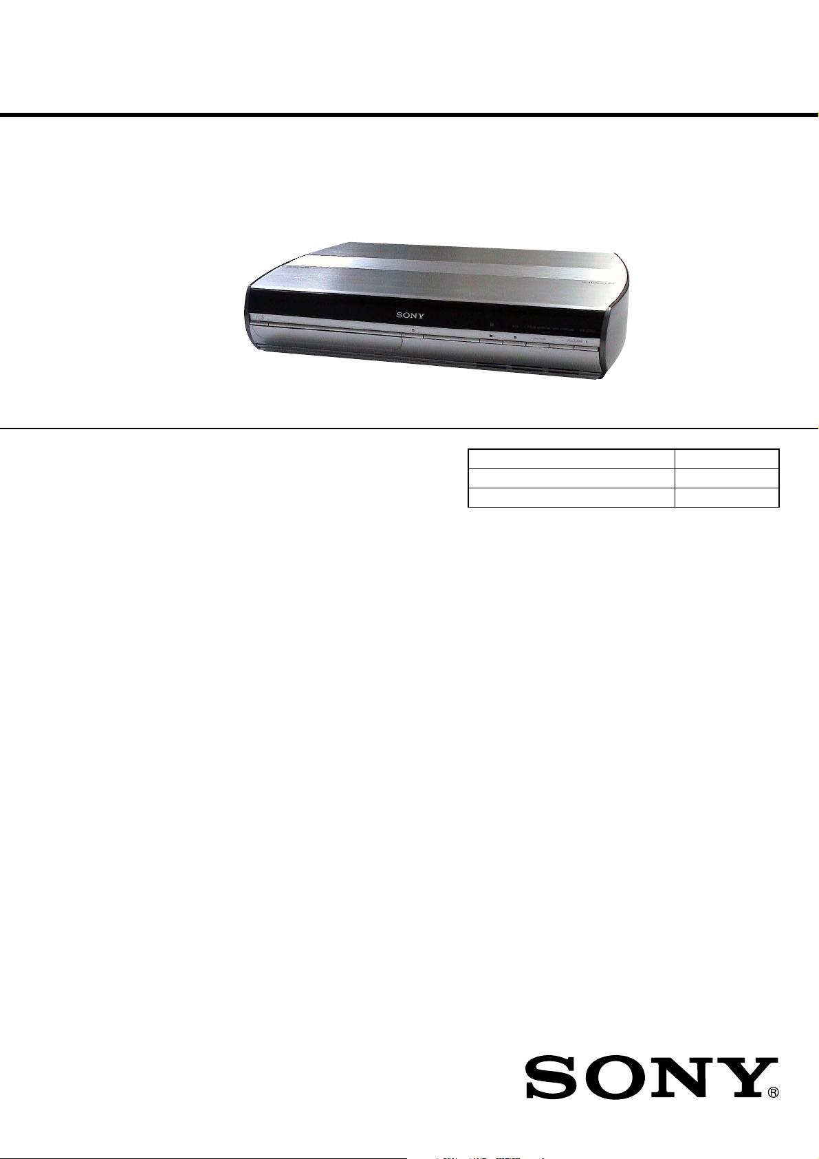
HCD-X1
SERVICE MANUAL
Ver. 1.2 2005.12
HCD-X1 is the amplifier, super audio CD/D VD system,
tuner and video section in DAV-X1.
This product incorporates copyright protection
technology that is protected by U.S. patents and
other intellectual property rights. Use of this
copyright protection technology must be
authorized by Macrovision, and is intended for
home and other limited viewing uses only unless
otherwise authorized by Macrovision. Reverse
engineering or disassembly is prohibited.
2
Digital
1
Digital
This system incorporates with Dolby*
and Dolby Pro Logic (II) adaptive matrix
surround decoder and the DTS*
Surround System.
US Model
Canadian Model
AEP Model
UK Model
E Model
Model Name Using Similar Mechanism NEW
DVD Mechanism Type CDM85-DVBU102
Optical Pick-up Block Name KHM-310CAA
SPECIFICATIONS
This system perfectly decodes 5.1 channel
signal, but you cannot add other commercially
available surround speakers.
*1 Manufactured under license from Dolby
Laboratories.
“Dolby,” “Pro Logic,” and the double-D symbo l are
trademarks of Dolby Laboratories.
*2 Manufactured under license from Digital Theater
Systems, Inc.
“DTS” and “DTS Digital Surround” are trademarks
of Digital Theater Systems , Inc.
9-879-627-03
2005L05-1
© 2005.12
Sony Corporation
Home Audio Division
Published by Sony Engineering Corporation
SUPER AUDIO CD/DVD RECEIVER
– Continued on next page –
Page 2
HCD-X1
r
Tuner section
System PLL quartz-locked digital
FM tuner section
Tuning range 87.5 – 108.0 MHz
Antenna (aerial) FM wire antenna (aerial)
Antenna (aerial) terminals 75 ohms, unbalanced
Intermediate frequency 10.7 MHz
AM tuner section
Tuning range
US, Canadian models: 530 – 1,710 kHz (with the
AEP, UK, Russian models:
Singapore model:
Antenna (aerial) AM loop antenna (aerial)
Intermediate frequency 450 kHz
Video section
Outputs Video: 1 Vp-p 75 ohms
Input VIDEO: 1 Vp-p 75 ohm s
General
Power requirements
US, Canadian models: 120 V AC, 60 Hz
except US, Canadian models:
Power consumption On: 85 W
Dimensions (approx.) 380 × 76 × 293 mm
Mass (approx.)
US, Canadian models: 4.6 kg (10 lb 3 oz)
except US, Canadian models:
Design and specifications are subject to change
without notice.
synthesizer system
US, Canadian models:
(100 kHz step)
except US, Canadian
models: (50 kHz step)
interval set at 10 kHz)
531 – 1,710 kHz (with the
interval set at 9 kHz)
531 – 1,602 kHz (with the
interval set at 9 kHz)
531 – 1,602 kHz (9 kHz)
530 – 1,710 (10 kHz)
S video:
Y: 1 Vp-p 75 ohms
C: 0.286 Vp-p 75 ohms
COMPONENT:
Y: 1 Vp-p 75 ohms
PB/CB, PR/CR: 0.7 Vp-p
75 ohms
S video:
Y: 1 Vp-p 75 ohms
C: 0.286 Vp-p 75 ohms
220 – 240 V AC, 50/60 Hz
Standby: 0.3 W (at the
Power Saving Mode)
(15 × 3 × 11
h/d) incl. projecting parts
4.5 kg
5
/8 inches ) (w/
Notes on chip component replacement
• Never reuse a disconnected chip component.
• Notice that the minus side of a tantalum capacitor may be
damaged by heat.
Flexible Circuit Board Repairing
• Keep the temperature of the soldering iron around 270 ˚C
during repairing.
• Do not touch the soldering iron on the same conductor of the
circuit board (within 3 times).
• Be careful not to apply force on the conductor when soldering
or unsoldering.
CAUTION
Use of controls or adjustments or performance of procedures
other than those specified herein may result in hazardous radiation
exposure.
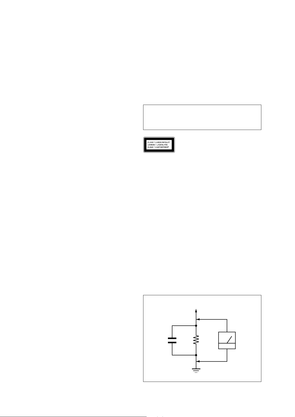
This appliance is classified as
a CLASS 1 LASER product.
The CLASS 1 LASER
PRODUCT MARKING is
located on the bottom of the unit.
SAFETY CHECK-OUT
After correcting the original service problem, perform the following
safety check before releasing the set to the customer:
Check the antenna terminals, metal trim, “metallized” knobs, screws,
and all other exposed metal parts for AC leakage.
Check leakage as described below.
LEAKAGE TEST
The AC leakage from any exposed metal part to earth ground and
from all exposed metal parts to any exposed metal part having a
return to chassis, must not exceed 0.5 mA (500 microamperes.).
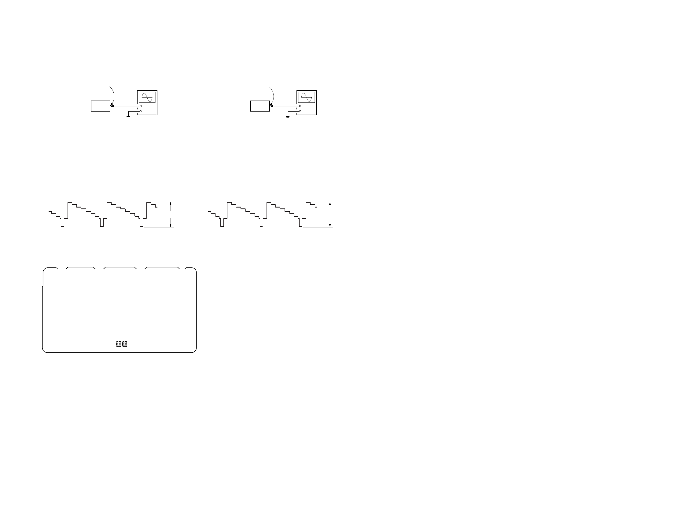
Leakage current can be measured by any one of three methods.
1. A commercial leakage tester, such as the Simpson 229 or RCA
WT -540A. Follow the manuf acturers’ instructions to use these
instruments.
2. A battery-operated A C milliammeter . The Data Precision 245
digital multimeter is suitable for this job.
3. Measuring the voltage drop across a resistor by means of a
VOM or battery-operated AC v oltmeter. The “limit” indication
is 0.75 V, so analog meters must have an accurate low-v oltage
scale. The Simpson 250 and Sanwa SH-63Trd are examples
of a passive VOM that is suitable. Nearly all battery operated
digital multimeters that have a 2 V A C range are suitable. (See
Fig. A)
SAFETY-RELATED COMPONENT WARNING!!
COMPONENTS IDENTIFIED BY MARK 0 OR DOTTED LINE
WITH MARK 0 ON THE SCHEMATIC DIAGRAMS AND IN
THE PARTS LIST ARE CRITICAL TO SAFE OPERATION.
REPLACE THESE COMPONENTS WITH SONY PARTS WHOSE
PART NUMBERS APPEAR AS SHOWN IN THIS MANUAL OR
IN SUPPLEMENTS PUBLISHED BY SONY.
ATTENTION AU COMPOSANT AYANT RAPPORT
À LA SÉCURITÉ!
LES COMPOSANTS IDENTIFIÉS P AR UNE MARQ UE 0 SUR
LES DIAGRAMMES SCHÉMATIQUES ET LA LISTE DES
PIÈCES SONT CRITIQUES POUR LA SÉCURITÉ DE
FONCTIONNEMENT. NE REMPLACER CES COM- POSANTS
QUE PAR DES PIÈCES SONY DONT LES NUMÉROS SONT
DONNÉS DANS CE MANUEL OU D ANS LES SUPPLÉMENTS
PUBLIÉS PAR SONY.
2
To Exposed Metal
Parts on Set
AC
0.15 µF
1.5 k
Ω
voltmete
(0.75 V)
Earth Ground
Fig. A. Using an AC voltmeter to check AC leakage.
Page 3
HCD-X1
About This Manual
•The instructions in this manual describe the
controls on the remote. You can also use the
controls on the s ystem if they have the sa me or
similar names as those on the remote.
•The Control Menu items may be different
depending on the area.
•“DVD” may be used as a general term for
DVD VIDEOs, DVD+RWs/DVD+Rs, and
DVD-RWs/DVD-Rs.
•Measurements are expressed in feet (ft) for
North American models.
•The following symbols are used in this
manual.
Symbol Meaning
Functions available for DVD
VIDEOs, DVD-Rs/DVD-RWs in
video mode, and DVD+Rs/
DVD+RWs
Functions available for DVD-RW s
in VR (Video Recording) mode
Functions available for VIDEO
CDs (including Super VCDs or CDRs/CD-RWs in vid eo CD f ormat or
Super VCD format)
Functions available for Super Audio
CDs
Functions available for music CDs
or CD-Rs/CD-R Ws in music CD
format
Functions available for DATA CDs
(CD-ROMs/CD-Rs/CD-RWs
containing MP3* audio tracks and
JPEG image files)
*MP3 (MPEG1 Audio Layer 3) is a standard format
defined by ISO/MPEG which compresses audio
data.
This System Can Play the
Following Discs
Format of
discs
DVD VIDEO
DVD-RW
VIDEO CD
Super Audio
*1
CD
*2
Audio CD
CD-R/CD-RW
(audio data)
(MP3 files)
(JPEG files)
The “DVD VIDEO” logo and “DVD-RW” logo are
trademarks.
*1Except for multi-channel playback area.
*2CD text data can be displaye d (album title only).
Note about CDs/DVDs
The system can play CD-ROMs/CD-Rs/CDRWs recorded in the foll owing format s:
–audio CD format
–video CD format
–MP3 audio tracks, JPEG image files, and
DivX video files of format conforming to ISO
9660 Level 1/ Le vel 2, or it s ext e nde d f or m at ,
Joliet
The system can play DVD-ROMs/DVD+RWs/
DVD-RWs/DVD+Rs/DVD-Rs recorded in the
following formats:
–DivX video files of format conforming to
UDF.
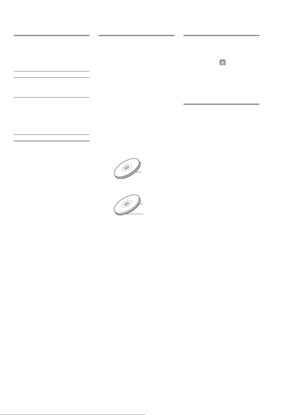
Disc logo
Example of discs that the
system cannot play
The system cannot play the following discs:
•CD-ROMs recorded in PHOTO CD format
•Data part of CD-Extras
• DVD Audios
• DVD-RAMs
•A DVD VIDEO with a different region code.
•A disc that has a non-standard shap e (e.g., car d
shaped, heart sha ped).
•A disc that has a commercially available
accessory attached, such as a label or ring.
Ring
Label
•An adapter to convert an 8 cm disc to standard
size.
•A disc with paper or stickers on it.
•A disc that has the adhesive of cellophane tape
or a sticker still left on it.
Notes about CD-R/CD-RW/DVD-R/
DVD-RW/DVD+R/DVD+RW
In some cases, CD-R/CD-RW/DVD-R/DVD-RW/
DVD+R/DVD+RW cannot be played on this system
due to the recording quality or physical condition of the
disc, or the characteristics of the recording device and
authoring software.
The disc will not play if it has not been correctly
finalized. For more information, see the operating
instructions for the recordi ng de vic e.
Note that discs created in the Packet Write format
cannot be played.
Music discs encoded with
copyright protection
technologies
This product is designed to play back dis cs tha t
conform to the Compact Disc (CD) standar d.
Recently, various music discs encoded with copyright
protection techn olo g ie s are ma rk ete d by some record
companies. Please be aware that among those discs,
there are some that do no t co nfor m to t he CD s tandar d
and may not be playable by this product.
Note on DualDisc
A DualDisc is a two sided disc product which mates
DVD recorded material on one side with digital audio
material on the other side. However, since the audio
material side does not conform to the Compact Disc
(CD) standard, playback on this product is not
guaranteed.
Note about DVD-RW (Except for
U.S./Canadian/European models)
Images in DVD-RWs with CPRM* protection may not
be played if they contain a copy protection signal.
“Copyright lock” appears on the screen.
*
CPRM (Content Pr otecti on for Reco rdable Me dia) is
a coding technology that protects the copyright of
images.
Adapter
3
Page 4
HCD-X1
Note on PBC (Playback
Control) (VIDEO CDs)
This system conforms to Ver. 1.1 and Ver. 2.0 of
VIDEO CD standards. You can enjoy two kinds
of playback depending on the disc type.
Disc type You can
VIDEO CDs
without PBC
functions
(Ver. 1.1 discs)
VIDEO CDs
with PBC
functions
(Ver. 2.0 discs)
Enjoy video playback (moving
pictures) as well as music.
Play interactive software using
menu screens displayed on the
TV screen (PBC Playback), in
addition to the video playback
functions of Ver. 1.1 discs.
Moreover, you can play highresolution still pictures , if the y
are included on the disc.
About Multi Session CD
•This system can play Multi Session CDs when
an MP3 audio track i s contained in the first
session. Any subsequent MP3 audio t racks
recorded in later sessions can also be played
back.
•This system can play Multi Session CDs when
a JPEG image file is co ntained in the first
session. Any subsequent JPEG ima ge files
recorded in later sessions can also be played
back.
• If audio tracks and images in music CD format
or video CD format are recorded in the first
session, only the first session will be played
back.
About the Super Audio CD
Super Audio CD is a new hi gh-quality audio
disc standard where music is recorded in the
DSD (Direct Stream Digital) format
(conventional CDs are recorded in the PCM
format). The DSD format, using a sampling
frequency 64 times higher than that of a
conventional CD, and with 1-bit quantization ,
achieves both a wide frequency range and a wide
dynamic range ac ross the audible fre quency
range, and so provides music reproduction
extremely faithful to the original sound.
Types of Super Audio CDs
There are two types of dis cs, depending on the
Super Audio CD layer and CD layer
combination.
••Super Audio CD layer: A high-densi t y
signal layer for Super Audio CD
CD layer*
conventional CD pl ayer
Single layer disc
(a disc with a single Super Audio CD layer)
Hybrid disc*
(a disc with an Super Audio CD layer and a CD layer)
*1You can play the CD layer on a conventional CD
player.
*2Since both layers are on one side, it is not necessary
to turn the disc over.
*3To select a layer, see “Selecting a Playback layer fo r
a Super Audio CD”.
1
: A layer that is readable by a
Super Audio CD
layer
2
CD layer*
Super Audio CD
3
layer*
3
Region code
Your system has a region code printed on th e
back of the unit and will only play DVDs labeled
with the same region code.
DVD VIDEOs labeled will also play on this
ALL
system.
If you try to play any other DVD VIDEO, the
message [Playback prohibited by area
limitations.] will appear on the TV screen.
Depending on the DVD VIDE O, no re gion co de
indication may be given even thoug h playing th e
DVD VIDEO is prohibited by area restrictions.
Note on playback operations
of DVDs and VIDEO CDs
Some playback operations of DVDs and VIDEO
CDs may be intentionally set by software
producers. Since this system plays DVDs and
VIDEO CDs according to the disc contents the
software producers designed, some playback
features may not be available. Also, refer to the
instructions supplied with the DVDs or VIDEO
CDs.
4
Page 5

TABLE OF CONTENTS
HCD-X1
1. SERVICING NOTES ............................................... 6
2. GENERAL ................................................................... 10
3. DISASSEMBLY
3-1. Disassembly Flow ........................................................... 12
3-2. Optical Pick-up Block (KHM-310CAA) ........................ 12
3-3. Side Panel (L/R) .............................................................. 13
3-4. Case (AL) ........................................................................ 13
3-5. Front Panel Section ......................................................... 14
3-6. MAIN Board.................................................................... 15
3-7. D.C. Fan (M450), Back Panel Section ............................ 15
3-8. DVD Mechanism Deck (CDM85-DVBU102) ................ 16
3-9. Chuck Cam, Belt ............................................................. 17
4. TEST MODE.............................................................. 18
5. ELECTRICAL ADJUSTMENTS ......................... 21
6. DIAGRAMS
6-1. Block Diagram – RF SERVO/VIDEO Section – ............ 22
6-2. Block Diagram
– HDMI Section (US and Canadian models) – ............... 23
6-3. Block Diagram – MAIN Section –.................................. 24
6-4. Block Diagram – AMP Section – .................................... 25
6-5. Block Diagram
– PANEL/POWER SUPPLY Section – ........................... 26
6-6. Printed Wiring Boards – DMB10 Section (1/2) – ........... 28
6-7. Printed Wiring Board – DMB10 Section (2/2) –............. 29
6-8. Schematic Diagram – DMB10 Section (1/4) – ............... 30
6-9. Schematic Diagram – DMB10 Section (2/4) – ............... 31
6-10. Schematic Diagram – DMB10 Section (3/4) – ............... 32
6-11. Schematic Diagram – DMB10 Section (4/4) – ............... 33
6-12. Printed Wiring Board – MIB01 Board (Component Side)
(US and Canadian models) –........................................... 34
6-13. Printed Wiring Board – MIB01 Board (Conductor Side)
(US and Canadian models) –........................................... 35
6-14. Schematic Diagram
– MIB01 Board (1/5) (US and Canadian models) –........ 36
6-15. Schematic Diagram
– MIB01 Board (2/5) (US and Canadian models) –........ 37
6-16. Schematic Diagram
– MIB01 Board (3/5) (US and Canadian models) –........ 38
6-17. Schematic Diagram
– MIB01 Board (4/5) (US and Canadian models) –........ 39
6-18. Schematic Diagram
– MIB01 Board (5/5) (US and Canadian models) –........ 40
6-19. Schematic Diagram – IO Board – ................................... 41
6-20. Printed Wiring Board
– IO Board (Component Side) –...................................... 42
6-21. Printed Wiring Board
– IO Board (Conductor Side) – ....................................... 43
6-22. Printed Wiring Board
– SCART Board (AEP, UK and Russian models) – ........ 44
6-23. Schematic Diagram
– SCART Board (AEP, UK and Russian models) – ........ 45
6-24. Printed Wiring Board
– MAIN Board (Component Side) – ............................... 46
6-25. Printed Wiring Board
– MAIN Board (Conductor Side) – ................................. 47
6-26. Schematic Diagram – MAIN Board (1/4) – .................... 48
6-27. Schematic Diagram – MAIN Board (2/4) – .................... 49
6-28. Schematic Diagram – MAIN Board (3/4) – .................... 50
6-29. Schematic Diagram – MAIN Board (4/4) – .................... 51
6-30. Printed Wiring Board – SWITCH Board – ..................... 52
6-31. Schematic Diagram – SWITCH Board – ........................ 53
6-32. Printed Wiring Board – FL Board – ................................ 54
6-33. Schematic Diagram – FL Board – ................................... 55
6-34. Printed Wiring Board
– POWER-AMP Board (Component Side) –.................. 56
6-35. Printed Wiring Board
– POWER-AMP Board (Conductor Side) –.................... 57
6-36. Schematic Diagram – POWER-AMP Board (1/3) –....... 58
6-37. Schematic Diagram – POWER-AMP Board (2/3) –....... 59
6-38. Schematic Diagram – POWER-AMP Board (3/3) –....... 60
7. EXPLODED VIEWS
7-1. Case (AL), Side Panel Section ........................................ 90
7-2. Front Panel Section ......................................................... 91
7-3. MAIN Board Section....................................................... 92
7-4. POWER-AMP Board Section ......................................... 93
7-5. Chassis Section................................................................ 94
7-6. DVD Mechanism Deck Section (CDM85-DVBU102) ... 95
8. ELECTRICAL PARTS LIST................................ 96
5
Page 6
HCD-X1
0RESSYTOSTOPTHEDISCTHENPRESS;TOEJECTTHEDISC
0RESS;TOLOADTHE3ETUP$ISCONTHETRAYTHENPRESS;
4HE3ETUP$ISCMENUAPPEARS
&
/
;
3ITINTHELISTENINGPOSITIONTHENSELECTONEOFTHETHREEOPTIONSONTHESCREENUSING$DAND
PRESS/OR%.4%2
4HESELECTEDOPTIONSTARTS
$D
%.4%2
0OSITIONTHESPEAKERSFORTHEBESTSOUNDEFFECT
,ISTENINGCAREFULLYTOHOWTHEOPTIONSOUNDSTODETERMINETHEBESTPOSITIONFORTHESPEAKERS)FASATISFACTORY
SURROUNDSOUNDEFFECTCANNOTBEACHIEVEDADJUSTTHESPEAKERPOSITIONS
(INT
"
0LACEBOTHFRONTSPEAKERSTHESAMEDISTANCEAPARTASTHEYAREFROMTHELISTENINGPOSITIONTOFORMANEQUILATERAL
TRIANGLE
#
4HEFRONTSPEAKERSSHOULDBEPLACEDATLEASTMFTAPART
$
4HEFRONTSPEAKERSSHOULDBEPLACEDATEARLEVELINTHELISTENINGPOSITION
%
0LACETHEFRONTSPEAKERSFORWARDOFTHE46-AKESURETHEREARENOREmECTINGOBSTACLESINFRONTOFTHESPEAKERS
&
"OTHFRONTSPEAKERSSHOULDBEPOINTEDSTRAIGHTFORWARD$ONOTPLACETHESPEAKERSATANANGLE
'
$ONOTLEAVEASPACEINFRONTOFTHEFRONTSPEAKERSWHENPLACEDONATABLEORRACKETCASREmECTIONMAYOCCUR
.OTE
s %VENIFANOPTIONISSELECTEDTHESOUNDVOLUMEOFTHESUBWOOFERMAYBELOW4HISISBYDEFAULTSETTINGANDISNOT
AMALFUNCTION
s 4HEEFFECTIVEAREAOFSURROUNDSOUNDWILLVARYDEPENDINGONTHESOUNDlELDSELECTION&/#533522/5.$OR
7)$%3522/5.$9OUCANCHANGETHESOUNDlELDSETTINGSFOROPTIMALFRONTSURROUNDSOUNDEFFECT&ORDETAILS
SEEh3YSTEM3OUND&EATUREvOFTHE/PERATING)NSTRUCTIONS
Ver. 1.2
SECTION 1
SERVICING NOTES
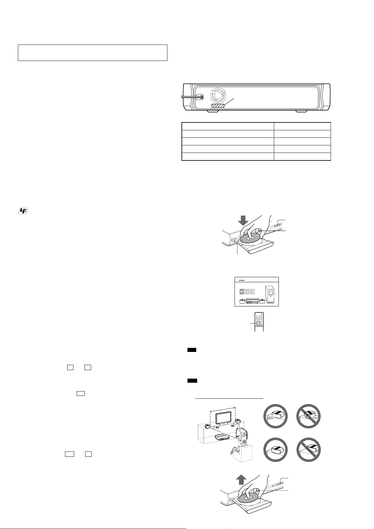
NOTES ON HANDLING THE OPTICAL PICK-UP
BLOCK OR BASE UNIT
The laser diode in the optical pick-up block may suffer electrostatic
break-down because of the potential difference generated by the
charged electrostatic load, etc. on clothing and the human body.
During repair, pay attention to electrostatic break-down and also
use the procedure in the printed matter which is included in the
repair parts.
The flexible board is easily damaged and should be handled with
care.
NOTES ON LASER DIODE EMISSION CHECK
The laser beam on this model is concentrated so as to be focused on
the disc reflective surface by the objective lens in the optical pickup block. Therefore, when checking the laser diode emission,
observe from more than 30 cm away from the objective lens.
UNLEADED SOLDER
Boards requiring use of unleaded solder are printed with the leadfree mark (LF) indicating the solder contains no lead.
(Caution: Some printed circuit boards may not come printed with
the lead free mark due to their particular size)
: LEAD FREE MARK
Unleaded solder has the following characteristics.
• Unleaded solder melts at a temperature about 40 °C higher
than ordinary solder.
Ordinary soldering irons can be used but the iron tip has to be
applied to the solder joint for a slightly longer time.
Soldering irons using a temperature regulator should be set to
about 350 °C.
Caution: The printed pattern (copper foil) may peel away if
the heated tip is applied for too long, so be careful!
• Strong viscosity
Unleaded solder is more viscou-s (sticky, less prone to flow)
than ordinary solder so use caution not to let solder bridges
occur such as on IC pins, etc.
• Usable with ordinary solder
It is best to use only unleaded solder but unleaded solder may
also be added to ordinary solder.
board, be sure to throw away after destroying IC602 physically with
the hammer etc.
• MODEL IDENTIFICATION
– Back Panel –
PART No.
MODEL PART No.
US and Canadian model 2-588-835-0[]
AEP and UK model 2-588-835-1[]
Russian model 2-588-835-2[]
Singapore model 2-588-835-4[]
S-FORCE FRONT SURROUND OPERATION CHECK
When complaint by the effect of the sound field, check as follows
and confirm abnormality is not found in the set.
Procedure:
RELEASING THE DISC TRAY LOCK
The disc tray lock function for the antitheft of an demonstration
disc in the store is equipped.
Releasing Procedure :
Press two buttons of Z and x simultaneously for five seconds.
The message “UNLOCKED” is displayed and the tray is unlocked.
Note: When “LOCKED” is displayed, the tray lock is not released by turning
power on/off with the I/1 button.
NOTE OF REPLACING THE DMB10 BOARD
New part of EEPROM (IC103) on the DMB10 board cannot be
used. Therefore, if the mounted DMB10 board is replaced, exchange
new EEPROM with that used before the replacement.
RELEASING THE DEMO PLAY LOCK
Releasing Procedure:
Press two buttons of N and x .
The message “DEMO OFF”.
NOTE OF HANDLING THE MIB01 BOARD (Part No. A1124-106-A)
When the MIB01 board is replaced by a repair for a fee, throw
away the MIB01 board after obtaining consent of not returning of
the MIB01 board to the customer. When thro wing away the MIB01
6
MFT^
^
"
%
&
'
Y
;
Page 7
Note: Follow the disassembly procedure in the numerical order given.
HOW TO OPEN THE LOADING ASSY PANEL WHEN POWER SWITCH TURNS OFF
2
Slide the chuck cam in the direction
of arrow to release the chucking.
1
Open the cover dust.
HCD-X1
3
Draw out the loading assy panel
in the direction of the arrow.
DMB10 BOARD SERVICE POSITION
• In checking the DMB10 board, prepare four extension jigs (Part No. J-2501-239-A: 1.00 mm Pitch, 5 cores, Length 300 mm, Part No.
J-2501-242-A: 1.00 mm Pitch, 11 cores, Length 300 mm and Part No. J-2501-280-A: 5 cores, Length 300 mm).
Connect extension jig (J-2501-242-A) to the
MAIN board (CN503) and DMB10 board (CN106).
DMB10 board
(CN202)
DMB10 board
(CN101)
wire (flat type) 24 core
Note: Don’t remove the
wire (flat type) 24 core (CN101).
If you remove the
wire (flat type) 24 core (CN101),
solder the bridge of optical pick-up.
DMB10 board
(CN106)
DMB10 board
(CN401)
DMB10 board
(CN4501)
Connect extension jig (J-2501-280-A) to the
MAIN board (CN508) and DMB10 board (CN401).
Connect extension jig (J-2501-242-A) to the
MAIN board (CN504) and DMB10 board (CN4501).
MAIN board
(CN504)
MAIN board
(CN508)
MAIN board
(CN503)
MS-203 board
(CN001)
Connect extension jig (J-2501-239-A) to the
DMB10 board (CN202) and MS-203 (CN001) board.
7
Page 8
HCD-X1
MAIN BOARD SERVICE POSITION
• In checking the MAIN board, prepare two extension jigs (Part No. J-2501-243-A: 1.00 mm Pitch, 17 cores, Length 300 mm and Part
No. J-2501-244-A: 1.00 mm Pitch, 21 cores, Length 300 mm).
Connect extension jig (J-2501-244-A) to the
MAIN board (CN506) and POWER-AMP board (CN301).
MAIN board
(CN506)
MAIN board
(CN505)
Connect extension jig (J-2501-243-A) to the
MAIN board (CN505) and SWITCH board (CN801).
SWITCH board
(CN801)
MIB01 BOARD (US, Canadian MODELS) SERVICE POSITION
MIB01 board
Any to board
POWER-AMP board
(CN301)
8
Page 9
FRONT PANEL SECTION SERVICE POSITION
• In checking the front panel section, prepare extension jig (Part No. J-2501-243-A: 1.00 mm Pitch, 17 cores, Length 300 mm).
Connect extension jig (J-2501-243-A) to the
MAIN board (CN505) and SWITCH board (CN801).
MAIN board
(CN505)
HCD-X1
front panel section
SWITCH board
(CN801)
POWER-AMP BOARD SERVICE POSITION
• In checking the POWER-AMP board, prepare extension jig (Part No. J-2501-244-A: 1.00 mm Pitch, 21 cores, Length 300 mm).
Note: Remove the MAIN Board once, and then remove the POWER-AMP board.
After that, reinstall the MAIN Board and set this service position.
POWER-AMP board
(CN301)
Reconnect the
power cord.
Connect extension jig (J-2501-244-A) to the
MAIN board (CN506) and POWER-AMP board (CN301).
MAIN board
(CN506)
POWER-AMP board
MAIN board
9
Page 10
HCD-X1
Front panel
SECTION 2
GENERAL
This section is extracted from
instruction manual.
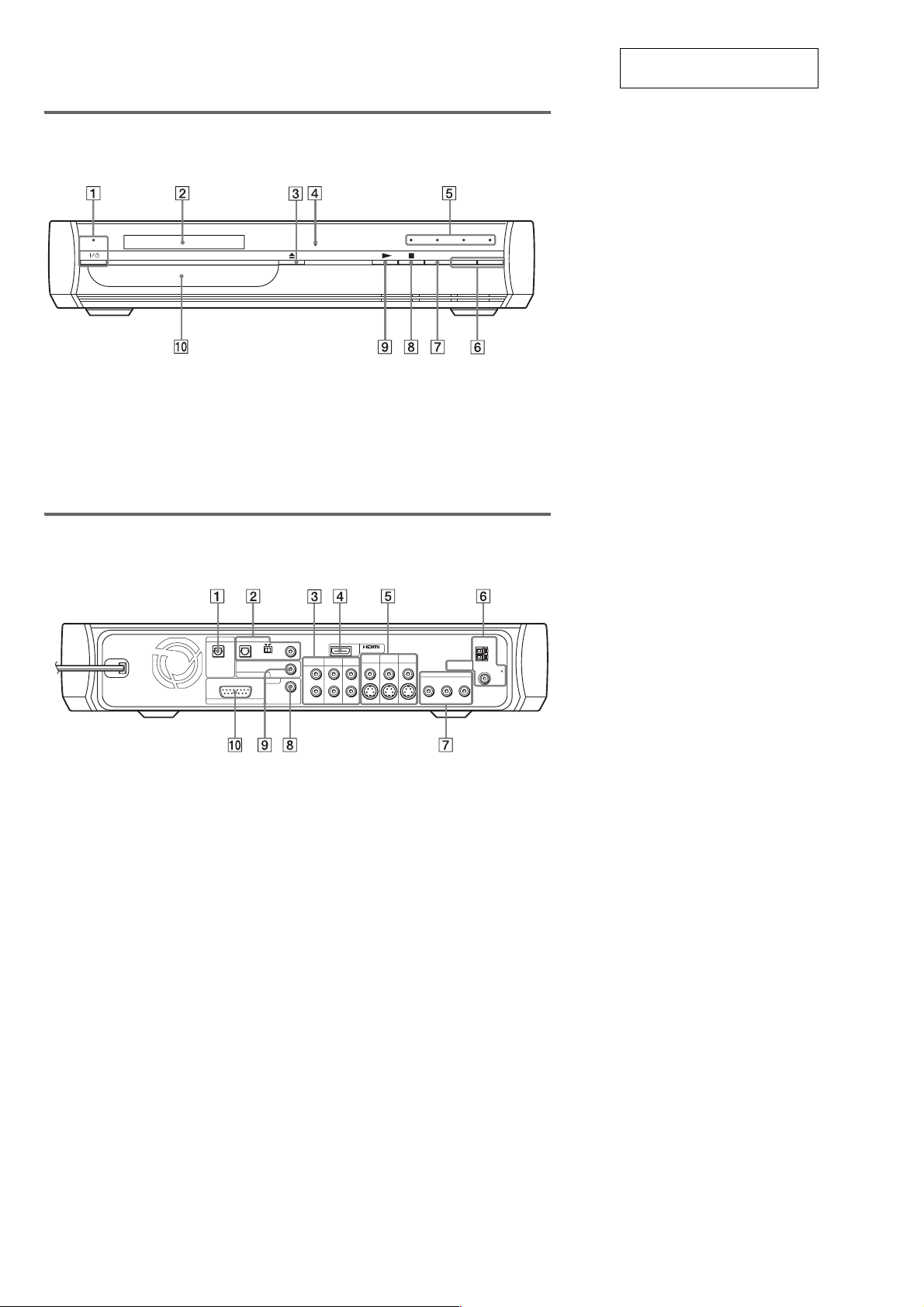
A "/1 (on/standby indicator)
B Front panel display
C Z (open/close)
D Remote sensor
E Sound Field indicator
F VOLUME –/+
G FUNCTION
H x (stop)
I N (play)
J Disc tray
Rear panel (US, Canadian, Singapore models)
DIGITAL OUT
VIDEO 1 / SAT 1
OPTICAL
DIGITAL IN
DIGITAL IN
SPEAKER
VIDEO 2 / SAT 2
COAXAL
OPTICAL
A DIGITAL OUT OPTICAL jack
B VIDEO 1/SAT 1 DIGITAL IN (OPTICAL/
COAXIAL) jacks
C AUDIO IN L/R (VIDEO 1/SAT1, VIDEO 2/
SAT 2, TV) jacks
D HDMI OUT jack
(US, Canadian models only)
E VIDEO/S-VIDEO IN (VIDEO 1/SAT 1,
VI
DEO 2/SAT 2, VIDEO/S-VIDEO OUT
(MONITOR OUT)) jacks
COAXIAL
VIDEO 1 /
SAT 1
L
TV
R
DIGITAL IN
COAXIAL
F ANTENNA (AM terminal/FM 75 Ω
G COMPONENT VIDEO OUT (Y, P
H TV DIGITAL IN COAXIAL jack
I VIDEO 2/SAT 2 DIGITAL IN (COAXIAL)
J SPEAKER jack
OUT
VIDEO 1 /
VIDEO 2 /
SAT 2
VIDEO 2 /
SAT 1
SAT 2
TV
VIDEO IN
VIDEO IN
S-VIDEO IN
S-VIDEO INAUDIO INAUDIO INAUDIO IN
COAXIAL jack)
C
R
) jacks
jack
MONITOR
S-VIDEO
OUT
VIDEO
ANTENNA
COMPONENT VIDEO OUT
YPB/CBPR/C
AM
FM
75
COAXIAL
R
B/CB
, PR/
10
Page 11
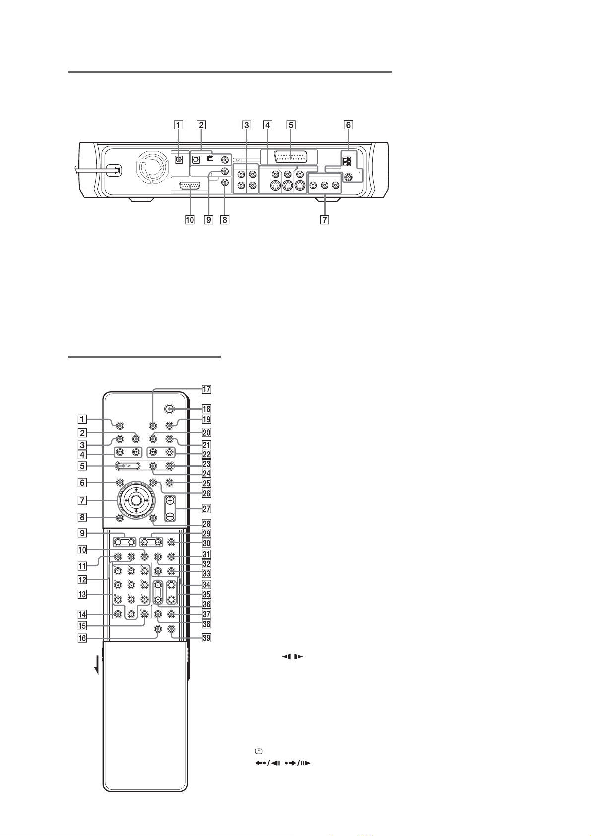
Rear panel (AEP, UK, Russian models)
DIGITAL OUT
VIDEO 1 / SAT 1
OPTICAL
COAXIAL
OPTICAL
SPEAKER
VIDEO 2 / SAT 2
DIGITAL IN
DIGITAL IN
COAXAL
OUTPUT(TO TV
VIDEO 2 /
VIDEO 1 /
SAT 2
SAT 1
L
TV
R
DIGITAL IN
COAXIAL
AUDIO INAUDIO IN
)
VIDEO 1 / SAT 1 VIDEO 2 / SAT 2
VIDEO IN
S-VIDEO IN
MONITOR OUT
S-VIDEO
VIDEO
COMPONENT VIDEO OUT
YPB/CBPR/C
ANTENNA
HCD-X1
AM
FM
75
COAXIAL
R
A DIGITAL OUT OPTICAL jack
B VIDEO 1/SAT 1 DIGITAL IN (OPTICAL/
COAXIAL) jacks
C AUDIO IN L/R (VIDEO 1/SAT1, VIDEO 2/
SAT 2, TV) jacks
D VIDEO/S-VIDEO IN (VIDEO 1/SAT 1,
VIDEO 2/SAT 2, VIDEO/S-VIDEO OUT
(MONITOR OUT)) jacks
E EURO AV T OUTPUT (TO TV) jack
Remote
Open the
cover.
F ANTENNA (AM terminal/FM 75 Ω
COAXIAL jack)
B/CB
G COMPONENT VIDEO OUT (Y, P
C
R
) jacks
, PR/
H TV DIGITAL IN COAXIAL jack
I VIDEO 2/SAT 2 DIGITAL IN (COAXIAL)
jack
J SPEAKER jack
A TV
B SLEEP
C SOUND FIELD
D ./> PRESET –/+, TV CH –/+
E H (play)
The H button has a tactile dot.*
F TOP MENU
G C/X/x/c/ENTER
have tactile dots.*
C/X/x/c
H O RETURN
I ALBUM –/+
J ANGLE
K AUDIO
The AUDIO button has a tactile dot.*
L SUBTITLE
M Number buttons
The number 5 button has a ta ct i le dot . *
N CLEAR, O ENTER
P PROGRESSIVE, TUNER MENU
Q TV [/1 (on/standby)
R "/1 (on/standby)
S THEATRE SYNC
T TV/VIDEO
U FUNCTION
V m/M / SLOW, TUNING –/+
W x (stop)
X X (pause)
Y MUTING
Z MENU
wj VOLUME, TV VOL +/–
The VOLUME, TV VOL + button has a
tactile dot.*
wk DISPLAY
wl /
REPLAY, ADVANCE,
STEP
e; DISPLAY
ea WOOFER
es PICTURE NAVI
ed REPEAT
ef FM MODE
eg TV CH –/+
The TV CH + button has a tactile dot.*
eh TV VOL +/–
ej NIGHT
ek SA-CD/CD
el AMP MENU
*Use the tactile dot as a refe rence when operatin g the
system.
11
Page 12
HCD-X1
• This set can be disassembled in the order shown below.
3-1. DISASSEMBLY FLOW
SET
SECTION 3
DISASSEMBLY
3-2. OPTICAL PICK-UP BLOCK (KHM-310CAA)
(Page 12)
3-3. SIDE PANEL (L/R)
(Page 13)
3-4. CASE (AL)
(Page 13)
3-5. FRONT PANEL SECTION
(Page 14)
3-6. MAIN BOARD
(Page 15)
3-7. D.C. FAN (M450), BACK PANEL SECTION
(Page 15)
3-8. DVD MECHANISM DECK (CDM85-DVBU102)
(Page 16)
3-9. CHUCK CAM, BELT
(Page 17)
Note: Follow the disassembly procedure in the numerical order given.
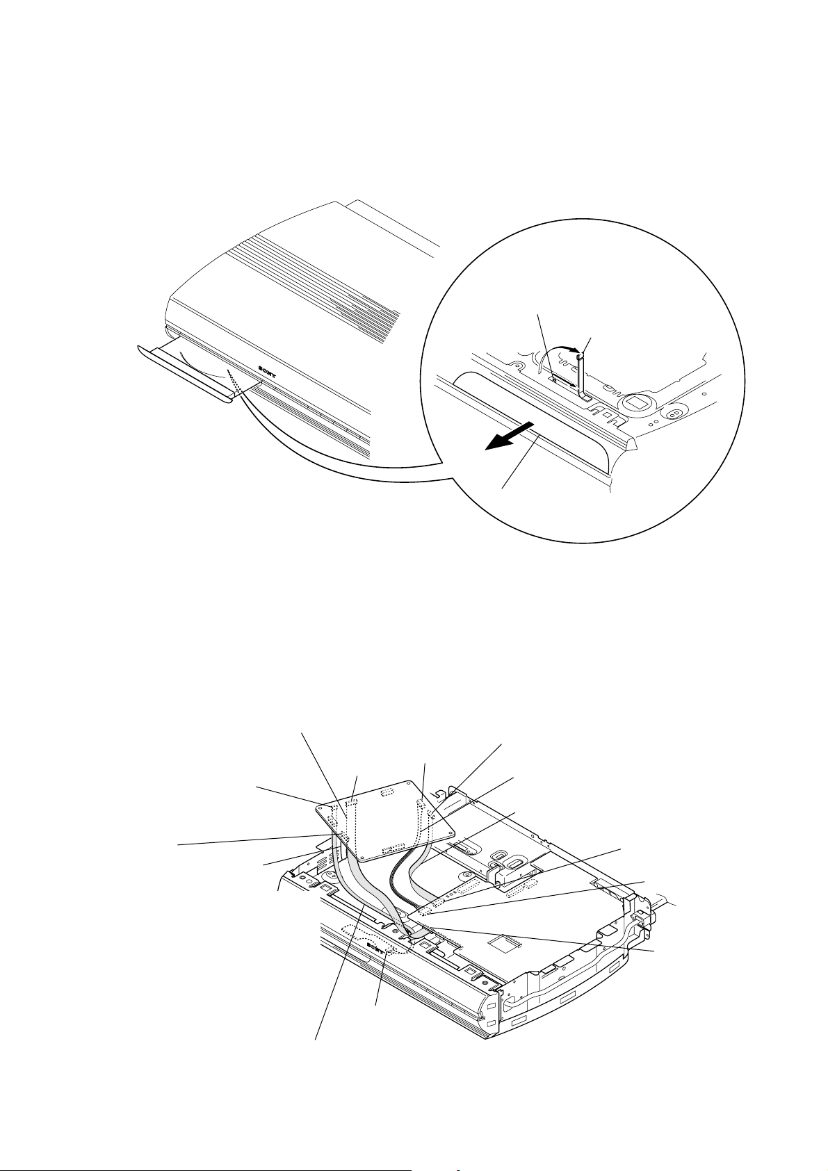
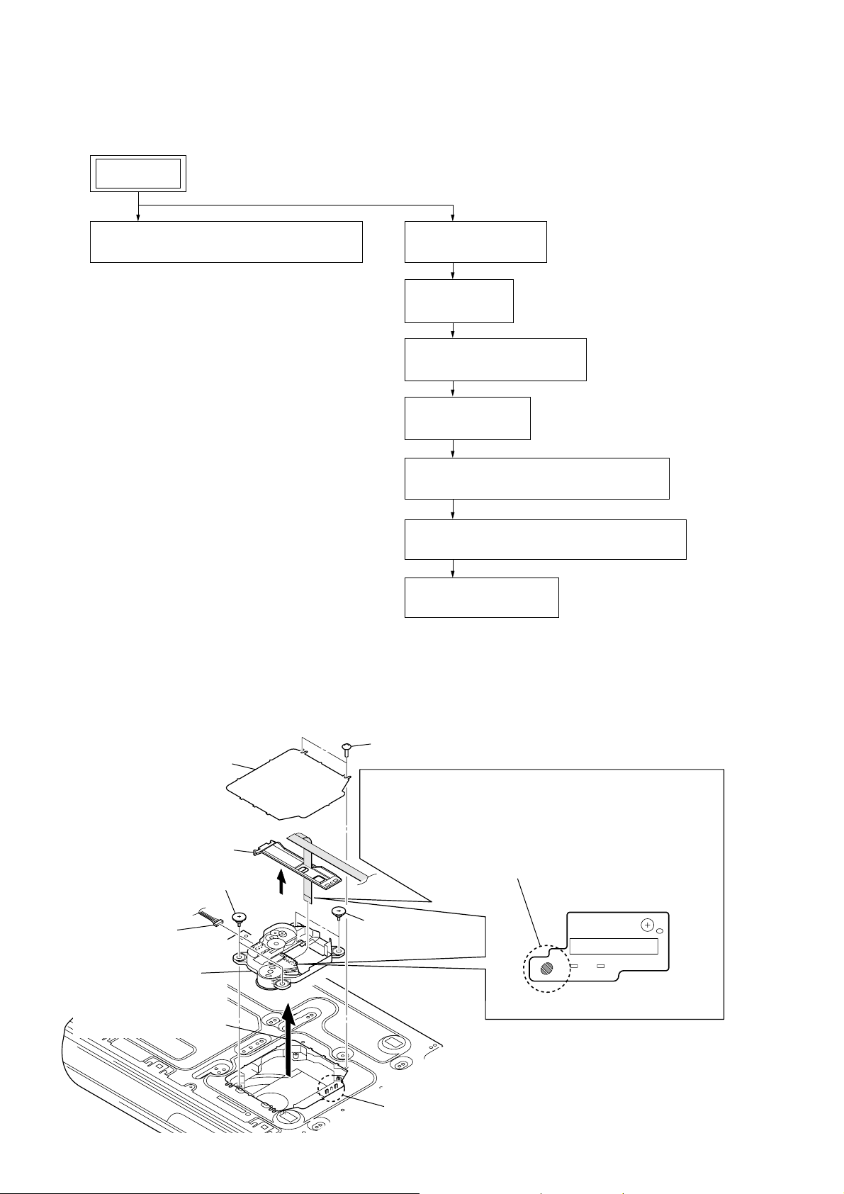
3-2. OPTICAL PICK-UP BLOCK (KHM-310CAA)
Note: The Cover (CDM) on the bottom of the set can be removed
when replacing the Optical Pick-up Block KHM-310CAA.
2
cover (CDM)
4
Lift up the holder (FFC).
5
two insulator screws
7
connector
9
optical-pick-up block
(KHM-310CAA)
6
Lift up the
optical-pick-up block.
1
two screws
(PTP 3
×
8)
PRECAUTION WHEN REMOVING GOOD OPTICAL PICK-UP BLOCK
8
Be sure to bridge here, and then disconnect the
wire (flat type) (24 core).
(optical pick-up block will be destroyed without bridging.)
On the contrary at the installation, connect the
wire (flat type) (24 core) first, and then remove the bridge.
Note: For a soldering iron, use the one with a ground wire.
5
two
insulator screws
12
3
two claws
Page 13
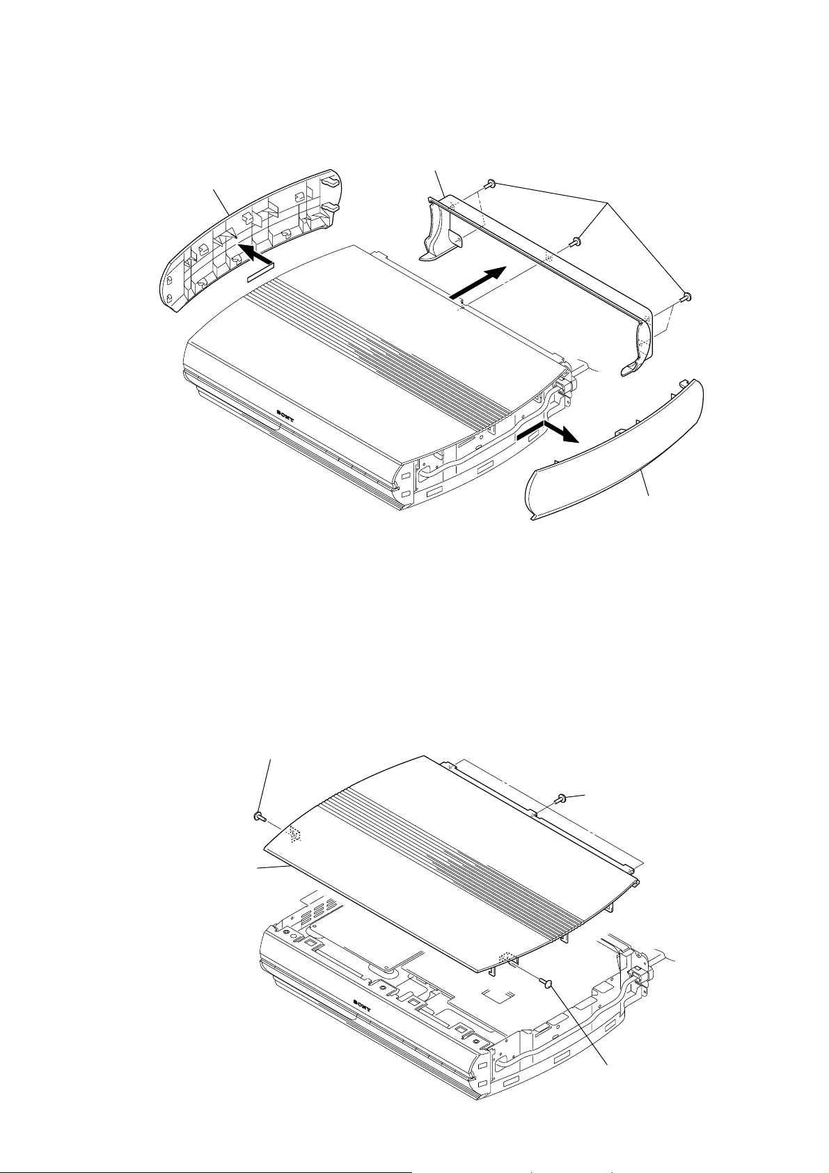
3-3. SIDE PANEL (L/R)
)
3
Remove the side panel (L)
in the direction of the arrow.
2
cover (rear)
1
five screws
(BVTP 3
HCD-X1
×
8)
3-4. CASE (AL)
2
case (AL)
1
screw
(BVTP 3
4
Remove the side panel (R)
in the direction of the arrow.
×
8)
1
three screws
(BVTP 3
×
8)
1
screw
(BVTP 3
×
8
13
Page 14
HCD-X1
Ver. 1.1
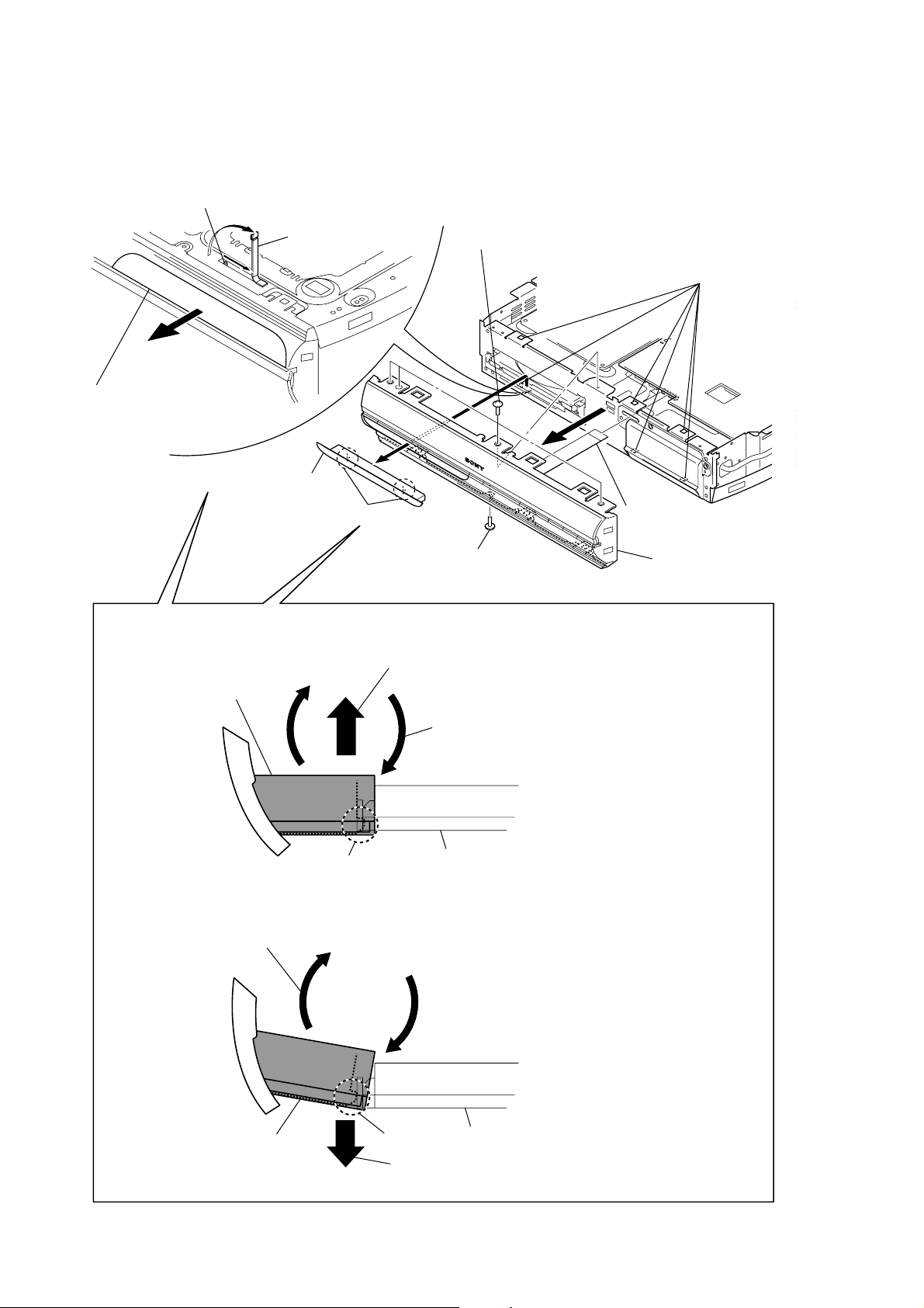
3-5. FRONT PANEL SECTION
2
Slide the chuck cam in the direction
of arrow to releae the chucking.
3
Draw out the loading assy panel
in the direction of the arrow.
5
loading assy panel
1
Open the cover dust.
6
four screws
(PTP 3 × 8)
9
six claws
4
two claws
– NOTE WHEN LOADING ASSY PANEL IS REMOVED –
2
Remove the loading assy panel while pulling it upward
until it is detached completely from the tray.
loading assy panel
claw
– NOTE WHEN LOADING ASSY PANEL IS INSTALLED –
1
Insert the loading assy panel while tilting it in the arrow direction.
(Tilt continuously a black part of loading assy panel.)
8
wire (flat type) (17 core)
(CN505)
7
screw
(BVTP 3 × 8)
1
Tilt the loading assy panel in the arrow direction
to disengage the claw.
(Tilt continuously a black part of loading assy panel.)
tray
q;
front panel section
14
loading assy panel
claw
2
Install the loading assy panel while pushing it downward until
the claw is locked completely.
tray
Page 15
HCD-X1
)
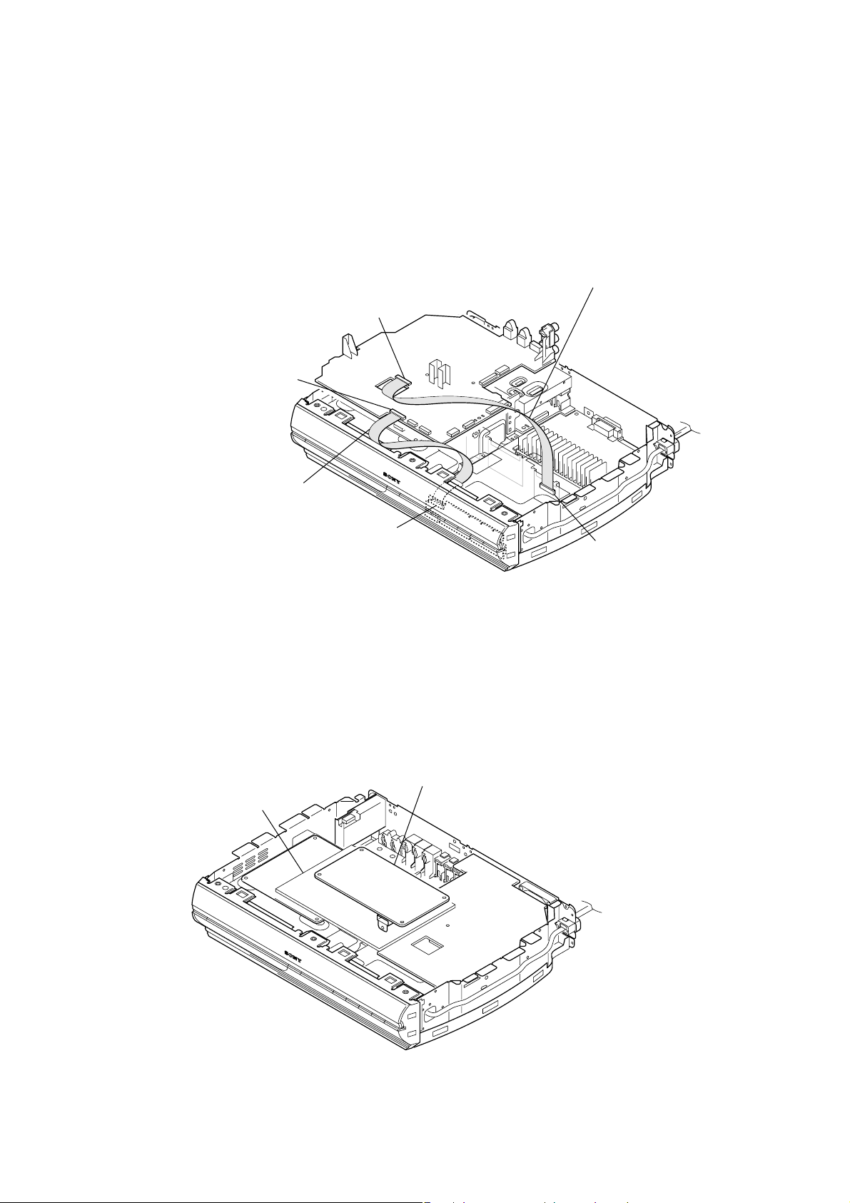
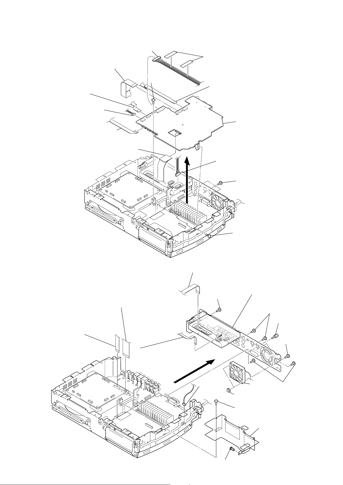
3-6. MAIN BOARD
3
wire (flat type) (11 core)
(CN504)
7
connector
(CN506)
4
wire (flat type) (11 core)
(CN503)
5
7
connector
(CN507)
2
wire (flat type) (19 core)
(CN501)
wire (flat type) (21 core)
(CN506)
8
screw
(BVTP 3
6
two saranet cushions
×
8)
1
wire (flat type) (9 core)
(AEP, UK, Russian and Singapore models),
wire (flat type) (11 core)
(US, Canadian models)
(CN502)
9
MAIN board
7
connector
(CN5101)
8
three screws
(BVTP 3
×
8)
3-7. D.C. FAN (M450), BACK PANEL SECTION
7
wire (flat type) (17 core)
(AEP, UK and Russian models)
(CN903)
6
wire (flat type) (13 core)
(CN902)
2
wire (flat type) (12 core)
(US, Canadian models)
(CN5201)
1
wire (flat type) (28 core)
(US, Canadian models)
(CN5401)
3
screw
(BVTP 3
5
8
connector
(CN450)
×
8)
8
screw
(BVTP 3
q;
qs
×
qs
back panel section
3
eight screws
(BVTP 3
qa
D.C. fan
(M450)
two nuts
(N3)
screw
(BV 3)
8)
×
8)
4
two screws
(supplied with
CN300)
9
two screws
(P 3
3
two screws
(BVTP 3
×
14)
×
8
qd
nylon rivet (DIA. 3.5)
qf
sheet (main)
15
Page 16
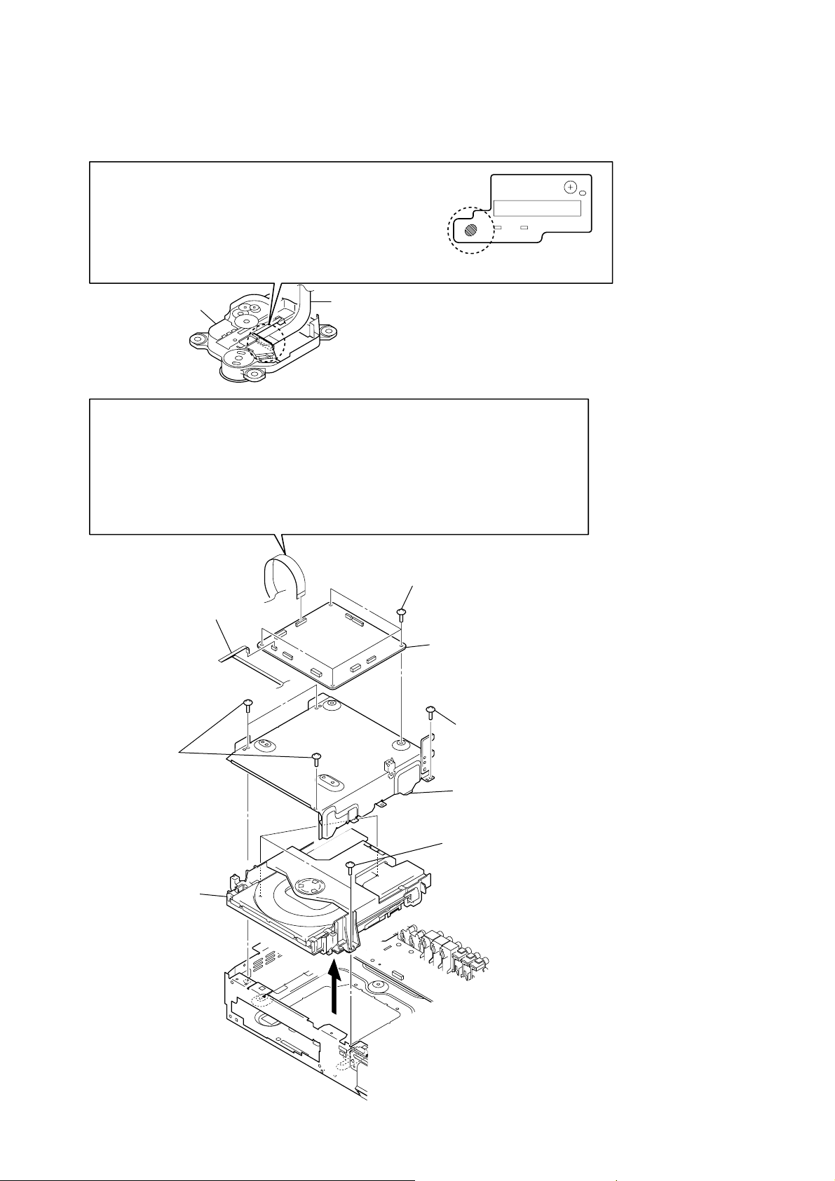
HCD-X1
”
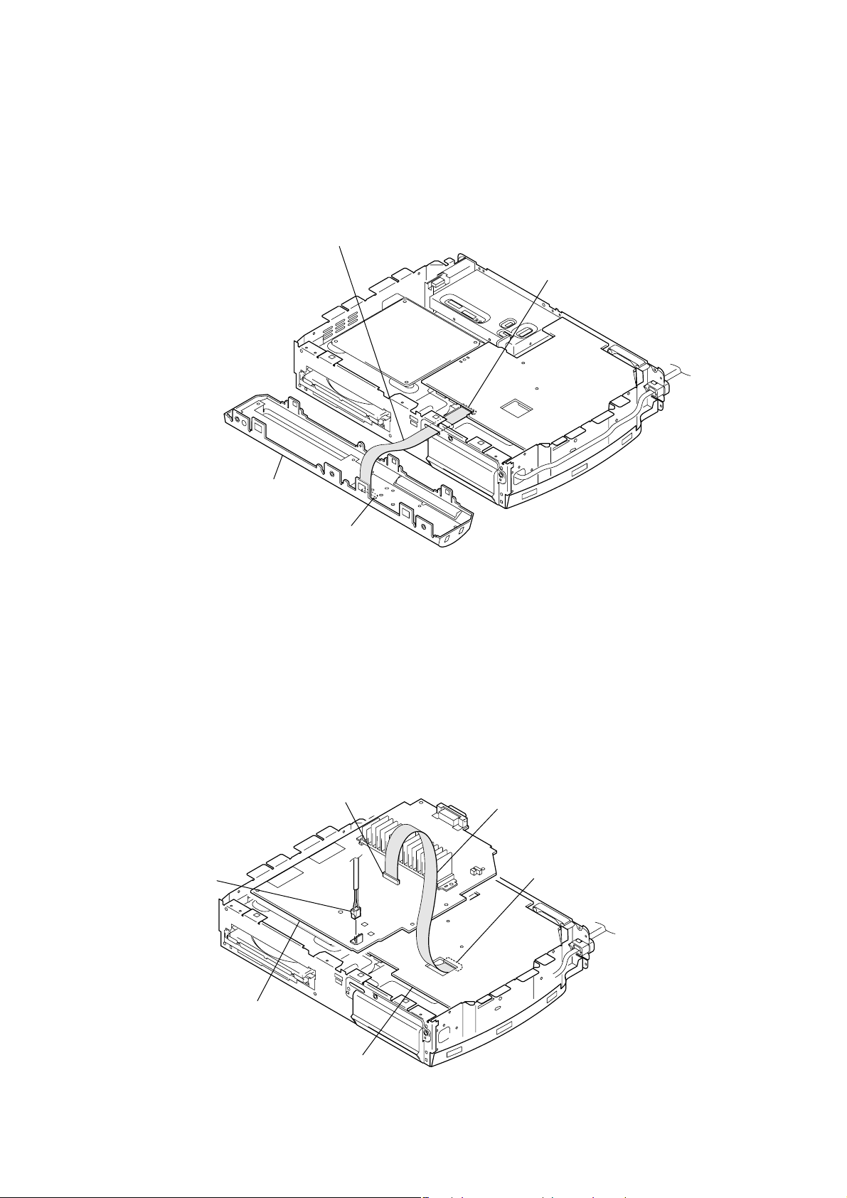
3-8. DVD MECHANISM DECK (CDM85-DVBU102)
PRECAUTION WHEN REMOVING GOOD OPTICAL PICK-UP BLOCK
Be sure to bridge here, and then disconnect the
wire (flat type) (24 core).
(optical pick-up block will be destroyed without bridging.)
On the contrary at the installation, connect the
wire (flat type) (24 core) first, and then remove the bridge.
Note: For a soldering iron, use the one with a ground wire.
(Refer to DISASSEMBLY 3-2. OPTICAL PICK-UP BLOCK (KHM-310CAA))
optical pick-up block
PRECAUTION WHEN REPLACING DVD MECHANISM DECK
(CDM85-DVBU102)
1
Perform work with this wire (flat type) (24 core) connected,
or make a bridge as mentioned above and then disconnect the wire (flat type) (24 core).
(optical pick-up will be destroyed without bridging.)
On the contrary at the installation, connect the wire (flat type) (24 core) first,
and then remove the bridge.
Note: For a soldering iron, use the one with a ground wire.
2
wire (flat type) (5 core)
(CN202)
wire (flat type) (24 core)
3
four screws
(BVTP 3
4
Note: Refer to SERVICING NOTES
×
8)
DMB10 board
“ NOTE OF REPLACING THE DMB10 BOARD
(page 6), when replacing the DMB10 board.
6
three screws
(BVTP 3
9
DVD mechanism deck
(CDM85-DVBU102)
×
8)
5
screw
(BV 3)
7
sub chassis
8
three screws
(BV 3)
16
Page 17
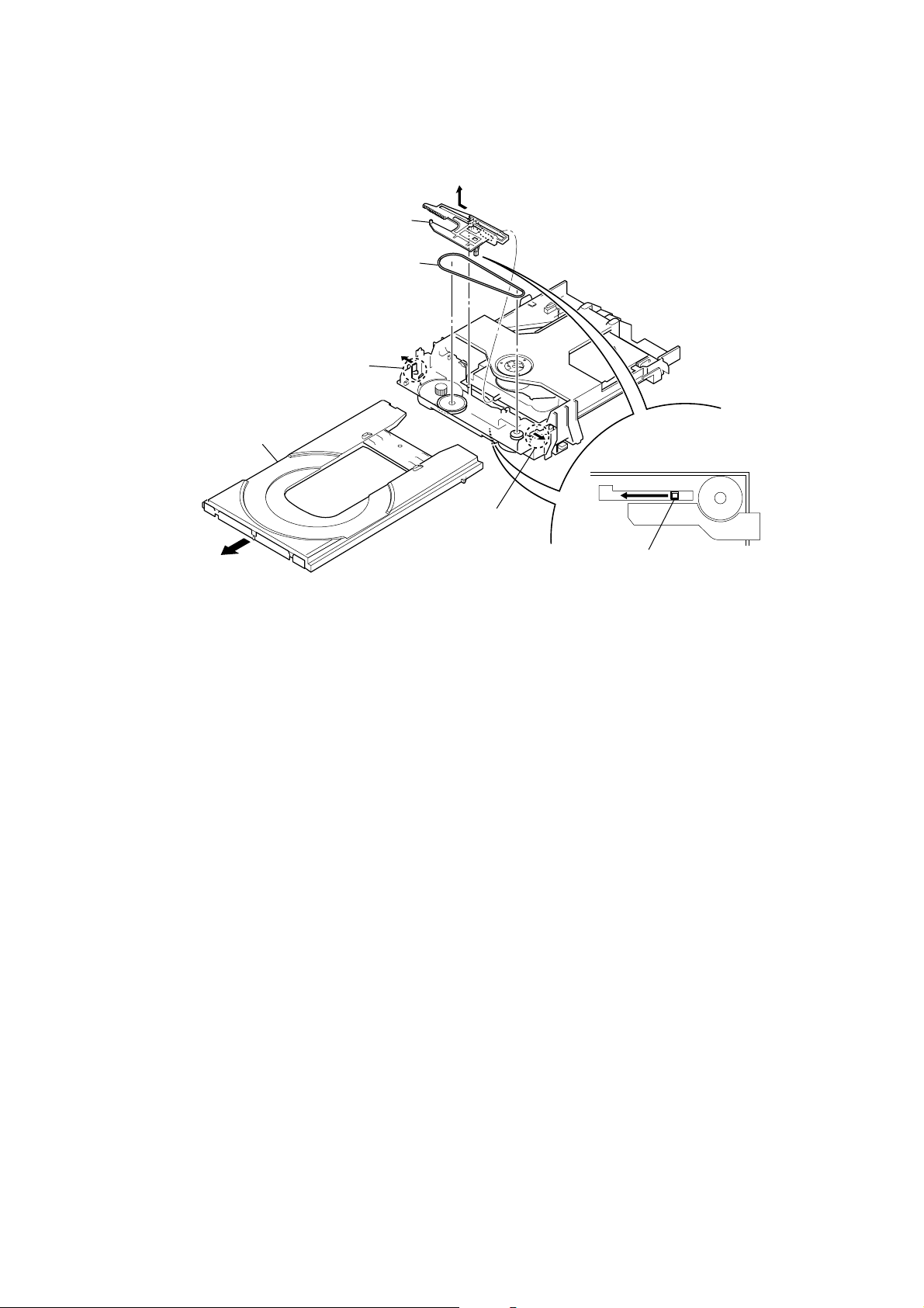
3-9. CHUCK CAM, BELT
4
tray
3
5
claw
chuck cam
6
belt
HCD-X1
2
3
claw
1
Slide the chuck cam in the direction
of arrow to releae the chucking.
17
Page 18

HCD-X1
SECTION 4
TEST MODE
COLD RESET
The cold reset clears all data including preset data stored in the
RAM to initial conditions. Execute this mode when returning the
set to the customers.
Procedure:
1. Set to the standby mode.
2. Press three buttons of I/1 , [FUNCTION] and [VOLUME --]
simultaneously.
3. The message “COLD RESET“ is displayed on the fluorescent
indicator tube, then becomes standby mode.
PANEL TEST MODE
This mode is used to check the fluorescent indicator tube, LED,
model, destination, software version and key.
Procedure:
1. Press three buttons of x , [FUNCTION] and [VOLUME +]
simultaneously.
2. All LEDs and segments in fluorescent indicator tube are lighted
up.
3. When you want to enter the software version display mode,
press the [VOLUME --]. The model name is displayed.
4. Each time [VOLUME --] is pressed, the display changes from
destination, MC ve rsion, SYS version, UI version, DVD
version, ST version, T A version, TM version in this order , and
returns to the model name display.
5. When [FUNCTION] button is pressed while the version numbers
are being displayed except model name and destination, the
date of the software creation appear. When [FUNCTION] button
is pressed again, the display returns to the software version
display. When [VOLUME --] is pressed while the date of the
software creation is being displayed, the date of the software
creation is displayed in the same order of software version
display.
6. Press the N button, the key check mode is activated.
7. In the key check mode, the fluorescent indicator tube displays
“K 0”. Each time a button is pressed, “K 0” value increases.
However , once a b utton has been pressed, it is no longer taken
into account.
8. To release from this mode, press three buttons in the same
manner as step 1 or disconnect the power cord.
SHIP MODE
This mode moves the optical pick-up to the position durable to
vibration. Use this mode when returning the set to the customer
after repair.
Procedure:
1. Press the I/1 button to turn the power on.
2. Press the [FUNCTION] button to select the “DVD”.
3. Press two buttons I/1 and x simultaneously.
4. The message “MECHA LOCK” is displayed on the fluorescent
indicator tube and the ship mode is set.
PRODUCT OUT
This mode moves the optical pick-up to the position durable to
vibration and clears all data including preset data stored in the RAM
to initial conditions. Use this mode when returning the set to the
customer after repair.
Procedure:
1. Set the DVD service mode. (See page 19)
2. Press the [4] key of the remote commander , and set the “V ersion
Information”.
3. Press the [DVD MENU] key of the remote commander.
4. Press the [CLEAR] key of the remote commander , the message
“Initialize all data” t “Complete” are displayed on the
fluorescent indicator tube.
5. Press the I/1 button to turn the power off.
6. Press the I/1 button to turn the power on.
7. Press the [FUNCTION] button to select the “DVD”.
8. Press three buttons of I/1 , Z and [VOLUME --] simultaneously .
9. After the “STANDBY” blinking display finish, the message
“MECHA LOCK” is displayed on the fluorescent indicator
tube and the ship mode is set.
TUNER STEP CHANGE
(US, Canadian and Singapore Models)
The step interval of AM channels can be toggled between 9 kHz
and 10 kHz.
Procedure:
1. Press the I/1 button to turn the power on.
2. Press the [FUNCTION] button to select the “TUNER AM”.
3. Press the I/1 button to turn the power off.
4. Press two buttons of I/1 and [FUNCTION] simultaneously. The
set power on automatically. The message “AM 9k Step” or
AM10k Step” displayed on the fluorescent indicator tube and
thus the channel step is changed.
COLOR SYSTEM CHANGE (Singapore Model)
This mode let you change the color system of the video output from
PAL to NTSC or vice-versa.
Procedure:
1. Press the I/1 button to turn the power on.
2. Press the [FUNCTION] button to select the “DVD”.
3. Press the I/1 button to turn the power off.
4. Press two buttons of I/1 and [VOLUME --] simultaneously.
5. The message “COLOR PAL” or “COLOR NTSC” will be
displayed on the fluorescent indicator tube
DSP SRAM CHECK
Procedure:
1. Press the I/1 button to turn the power on.
2. Press three buttons of x , N and [FUNCTION] simultaneously.
3. The message “RAM OK” (IC507 on the MAIN board is
normal) or “RAM NG” (IC507 on the MAIN board is
abnormal) will be displayed on the fluorescent indicator tube.
18
Page 19
HCD-X1
DVD SECTION
1. DVD SERVICE MODE GENERAL DESCRIPTION
The Mirror Time and IOP measurement allows you to make
diagnosis and adjustment simply by using the remote commander
and monitor TV. The instructions, diagnosis results, etc. are given
on the on-screen display (OSD).
2. STARTING DVD SERVICE MODE
1. Press the I/1 button to turn the power on.
2. Press the [FUNCTION] button to select the “DVD”.
3. Press three buttons x , Z and [VOLUME +] simultaneously.
4. The message “SERVICE IN” will be displayed on the
fluorescent indicator tube and the Rimocon Diagnosis Menu
is displayed on the on-screen display on the monitor TV as
follows. The model name, IF-con version and Syscon v ersion
is displayed at the bottom of the on-screen display.
Remocon Diagnosis Menu
0. External Chip Check
1. Servo Parameter Check
2. Drive Manual Operation
3. Emergency History
4. Version Information
5. Video Level Adjustment
4. MIRROR TIME ADJUSTMENT
On the Drive Manual Operation menu screen, press [5] button on
the remote commander, and the following MIRR time Adjust Menu
will be displayed.
MIRR time Adjust Menu
1. CD MIRR time Check:
2. DVD MIRR time Check:
3. Threshold:
4. Save to EEPROM
5. Default set MIRR time
[Open]Tray open [Close]Tray close
[0]Return to previous menu
There are five main commands in the Mirr time Adjust menu. The
functions of each command are described in the following page.
1. CD MIRR time Check
This command checks the Mirror time value for CD disc.
2. DVD MIRR time Check
This command checks the Mirror time value for DVD disc.
Model Name :xxxx
IF-con :Ver.xx.xx (xxxx)
Syscon :Ver.x.xxx
5. To execute each function, press its number by using numeric
button on the remote commander (RM-ADP004).
6. To release from this mode, press the I/1 button to turn the
power off.
3. DRIVE MANUAL OPERATION
The Drive Manual Operation menu consists of five main function.
On the Remocon Diagnosis Menu screen, press [2] button on the
remote commander, and the following Drive Manual Operation
menu will be displayed.
Drive Manual Operation
1. Servo Control
2. Track/Layer Jump
3. Manual Adjustment
4. Tray Aging Mode
5. MIRR time Adjust
0. Return to Top Menu
3. Threshold
This command displays the threshold value between CD and DVD
mirror time.
4. Save to EEPROM
This command saves an adjusted mirror time value to the EEPROM.
5. Default set MIRR time
This command will set CD and DVD mirror time to firmware default
value.
[Open] / [Close]
Pressing the Z button controls the tray for disc change during
mirror time adjustment.
[0] Return to previous menu
Press the [0] button on the romote commander to return to previous
menu.
EXECUTING MIRROR TIME ADJUSTMENT
In order to execute mirror time adjustment, the following standard
procedures must be followed.
1. Set to the MIRR time Adjust Menu mode.
2. Press the [5] button on the romote commander to select the
“5. Default set MIRR time”.
3. Press the [3] button on the romote commander to select the
“3. Threshold”.
4. Check the value of Threshold on the screen. If it is 75, go to
next step. If it is not so, return to step 2.
19
Page 20

HCD-X1
MIRR time Adjust Menu
17. Take out the CD test disc (YEDS-18).
18. Release the MIRR time Adjust Menu mode.
1. CD MIRR time Check:
2. DVD MIRR time Check:
3. Threshold:75
4. Save to EEPROM
5. Default set MIRR time
[Open]Tray open [Close]Tray close
[0]Return to previous menu
5. Insert the DVD test disc (HLX-504) (Part No. J-6090-088-A).
6. Press the [2] button on the romote commander to select the
“2. DVD MIRR time Check”.
7. Wait for hexadecimal value to display on the screen.
8. Check the value (##) of DVD MIRR time on the screen. If
## is 28 to 70, go to next step. If it is not so, return to step 5.
MIRR time Adjust Menu
1. CD MIRR time Check:
2. DVD MIRR time Check: $$ ##
3. Threshold:
4. Save to EEPROM
5. Default set MIRR time
[Open]Tray open [Close]Tray close
[0]Return to previous menu
9. Press the [4] button on the romote commander to select the
“4. Save to EEPROM”.
10. Check that $$ is the same as the value of ## on the screen. If
it is not so, return to step 5.
11. Tak e out the DVD test disc (HLX-504) and insert the CD test
disc (YEDS-18) (Part No. 3-703-998-01).
12. Press the [1] button on the romote commander to select the
“1. CD MIRR time Check”.
13. Wait for hexadecimal value to display on the screen.
14. Check the value (@@) of DVD MIRR time on the screen. If
@@ is 5A to E8, go to next step. If it is not so, return to step 11.
MIRR time Adjust Menu
1. CD MIRR time Check: && @@
2. DVD MIRR time Check: $$ ##
3. Threshold:
4. Save to EEPROM
5. Default set MIRR time
5. EXECUTING IOP MEASUREMENT
In order to execute IOP measurement, the following standard
procedures must be followed.
1. Set to the Drive Manual Operation mode.
2. Press the [3] button on the romote commander, and the
following Manual Adjust menu will be displayed.
Manual Adjust
1. Track Balance Adjust:
2. Track Gain Adjust:
3. Focus Balance Adjust:
4. Focus Gain Adjust:
5. Eq Boost Adjust:
6. Iop:
7. TRV. Level:
8. S curve(FE) Level:
9. RFL(PI) Level:
0. MIRR Time:
↓ ↑ Change Value
[RETURN]Return to previous menu
3. Press the [6] button on the romote commander to select the
“6. Iop”.
4. Wait for hexadecimal Value to display on the screen.
Manual Adjust
1. Track Balance Adjust:
2. Track Gain Adjust:
3. Focus Balance Adjust:
4. Focus Gain Adjust:
5. Eq Boost Adjust:
6. Iop: YY ZZ
7. TRV. Level:
8. S curve(FE) Level:
9. RFL(PI) Level:
0. MIRR Time:
↓ ↑ Change Value
[RETURN]Return to previous menu
5. Convert each value (YY and ZZ) from hexadecimal to decimal
using conversion table.
6. Substract between these two values (YY and ZZ).
7. If the remainder is smaller than 93 (decimal), then it is OK.
However if the value is higher than 93, then the BU (base
unit) is defective and need to be change.
8. Release the Manual Adjust menu mode.
[Open]Tray open [Close]Tray close
[0]Return to previous menu
15. Press the [4] button on the romote commander to select the
“4. Save to EEPROM”.
16. Check that && is the same as the value of @@ on the screen. If
it is not so, return to step 11.
20
Page 21
SECTION 5
ELECTRICAL ADJUSTMENTS
HCD-X1
CONPOSITE VIDEO OUT LEVEL ADJUSTMENT
(US and Canadian Models)
Setting:
IO board
MONITOR OUT
VIDEO jack (J904)
set
Procedure:
1. Insert the test disc (TDV-520CSO) (Part No.: J-2501-236-A),
and color bar mode is played.
2. Connect an oscilloscope to the MONITOR OUT VIDEO jack
(J904) on the IO board.
3. Input color bars signal from the color pattern generator.
4. Adjust the RV501 on the MIB01 board so that the Vp-p value
of waveform becomes 1 Vp-p.
waveform:
oscilloscope
(AC range)
+
–
1 Vp-p
COMPONENT VIDEO OUT LEVEL ADJUSTMENT
(US and Canadian Models)
Setting:
IO board
COMPONENT VIDEO
OUT Y jack (J905)
set
Procedure:
1. Insert the test disc (TDV-520CSO) (Part No.: J-2501-236-A),
and color bar mode is played.
2. Connect an oscilloscope to the COMPONENT VIDEO OUT
Y jack (J905) on the IO board.
3. Input color bars signal from the color pattern generator.
4. Adjust the RV502 on the MIB01 board so that the Vp-p value
of waveform becomes 1 Vp-p.
waveform:
oscilloscope
(AC range)
+
–
1 Vp-p
Adjustment Location:
– MIB01 Board (Component Side) –
RV501
RV502
HCD-X1
2121
Page 22
HCD-X1
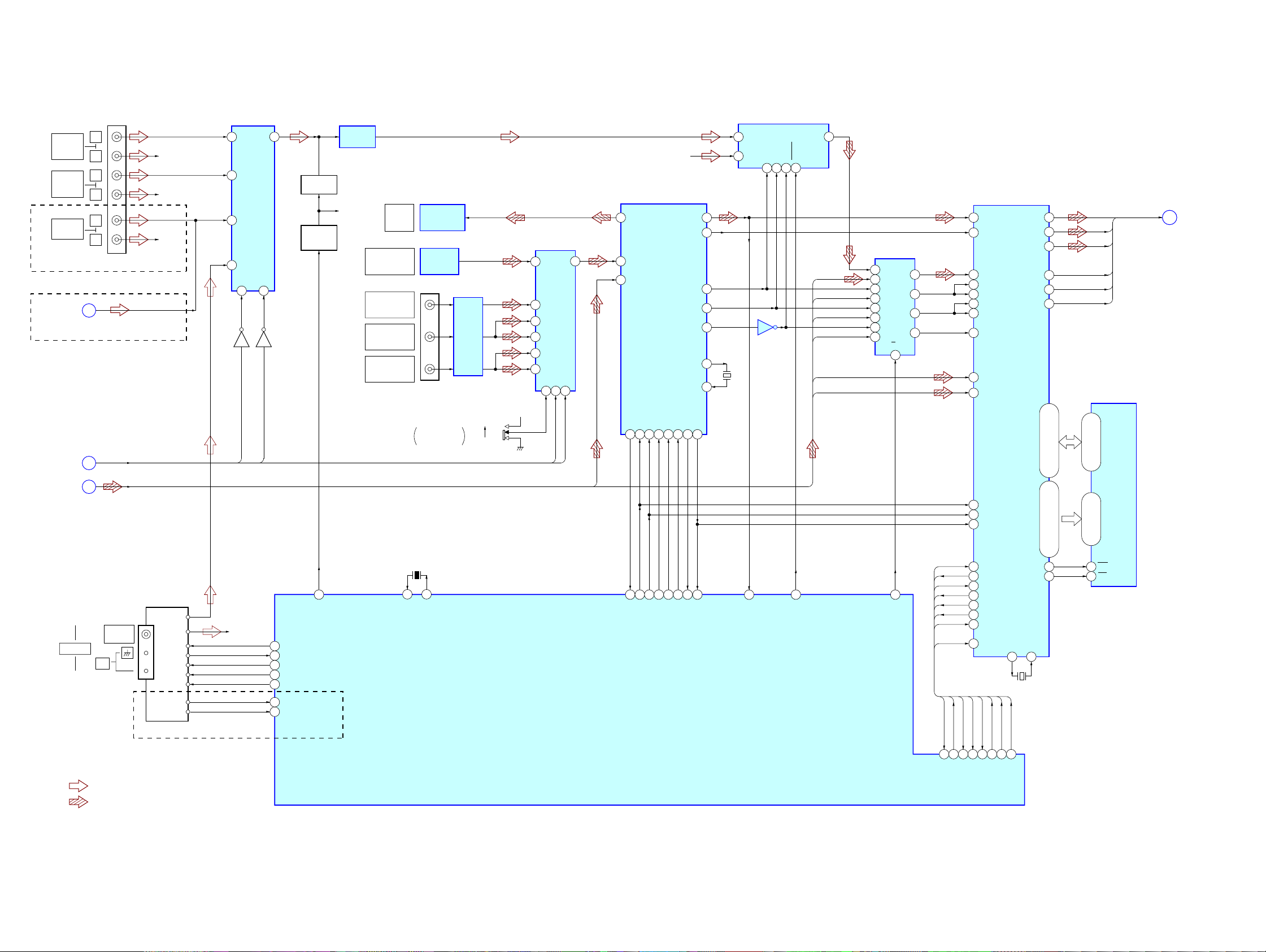
6-1. BLOCK DIAGRAM – RF SERVO/VIDEO Section –
SECTION 6
DIAGRAMS
VOA/A
VOB/B
VOC/C
VOD/D
OPTICAL PICK-UP
BLOCK
(KHM-310CAA)
VR (780)
MSW
FCS+
FCS– 37
TRK+ 35
TRK– 34
SL+ 29
SL– 30
SP+ 27
SP– 28
M301
DISC TRAY
OPEN/CLOSE
RF
PD
REGO2
REGO1
AUTOMATIC POWER
CONTROL (FOR CD)
Q102-2
AUTOMATIC POWER
CONTROL (FOR DVD)
Q102-1
VOLUME
CONTROL
Q101, 103
FOCUS/TRACKING COIL DRIVER,
SPINDLE/SLED/LOADING MOTOR DRIVER
36
46
47
M
25
24
42
31
32
IC201
FOCUS
COIL DRIVE
TRACKING
COIL DRIVE
MOTOR DRIVE
SPINDLE
MOTOR DRIVE
BUFFER
LOADING
MOTOR DRIVE
BUFFER
REGULATOR
SLED
MUTE5
DVD
6
11
13
15
RGB SELECT
Q954, 955,
Q959
DVD_SEL
VIDEO AMP, 75 Ω DRIVER
IC951
MUTE1
5
AV2
VOUT
CYOUT
CbOUT
CrOUT
MUTE2
14
VIDEO
MUTING
Q951, 952
RGB_SEL
AV3
34
12
34
12
34
12
Y
PB/CB
PR/CR
CVBS IN
CYIN
CbIN
CrIN
• R-ch is omitted due to same as L-ch.
• SIGNAL PATH
FUNCTION SW
BLANKING OUT
R-CH
S-VIDEO IN
VIDEO IN
S-VIDEO IN
VIDEO IN
S-VIDEO
VIDEO
J905
COMPONENT
VIDEO OUT
CVBS OUT
AV0, AV1
30, 29
24, 23
21, 20
18, 17
: AUDIO (ANALOG)
: AUDIO (DIGITAL)
: VIDEO
G OUT
B OUT
R/C OUT
A (L) IN
A (R) IN
T OUTPUT
TV
VIDEO 1/SAT 1
VIDEO 2/SAT 2
J904
MONITOR OUT
J951
(TO TV)
D
J902
J903
E
19
11
7
15
8
16
6
2
(Page 24)
(Page 24)
IC901
YOUT
C OUT.
S-DC OUT
VOUT
CYOUT
CbOUT
CrOUT
VIDEO
MUTING
Q901
(AEP, UK, Russian)
AV0
AV1
27, 26
32, 31
30, 29
24, 23
21, 20
18, 17
MUTE1
5
AV2
RGB_SEL
AV3
WIDE
RGB_SEL
AV1
AV2
AV3
82
83
84
AV SELECT 2
AV SELECT 3
WIDE
SWITCH
Q958
WIDE
DVD_SEL
AV0
D901
81
AV SELECT 1
AV SELECT 0
Q956, 957
Y1
C1
V1
Y2
C2
V2
+
DVD
SELECT
(AEP, UK, Russian)
D902
SELECT
Q903
ACLK
BA0 BA0
ASDATA0
ASDATA1
ASDATA2
SPDIF
ACLK
ABCK
ALRCK
LEVEL
SHIFT
IC4802
ABCK
Y1
Y2
C1
C2
V1
V2
21
38
37
145
156
157
113
BA1 BA1
CKE CKE
RCLK CLK
CKSW
OCKSW
179
177
217
ASDATA0
DVDRF
6
8
9
10
11
22LD (650)
187VR (650)
176LIMIT
1
4
10
13
45
16
17
15
19
21
20
22
40
8
186
185
39
184
RF+3.3V
ASDATA1 218
IP
ASDATA2 219
MA
MB
ASDATA4
MC
MD
DVDA2
DVDB3
DVDC4
DVDD5
TNI18VOE/E+G
TPI19VOF/F+H
V2O29VC
MDI120
MDI221
LDO123LD (780)
LDO2
MSW
LIMSW
RF AMP, SERVO DSP,
FOO42
TRO41
FMO38
DMO37
SPFG47
FWD
REV
TROPENPWM
MUTE123MUTE12
MUTEMUTE34 183
TSDMTSD-M 181
IOPMON40
SPDIF
ACLK 215
ABCK 214
ALRCK 213
SDA 103
SCL 102
VCLK
HSYNC
VSYNC
XRST
SMSDO
SMSDI
SMSCK
XSMCS
XSMRST
YUV0
YUV7
YUV1
YUV2
MPEG DECODER
IC102
YUV3
YUV4
YUV5
YUV6
66
11
222
225
5
EEPROM
IC103
178
207
205
220
210
209
208
211
170
192
206
194
196
198
200
202
203
2, 4, 5, 7, 8, 10, 11, 13, 42,
44, 45, 47, 48, 50, 51, 53
125 – 123, 121, 120, 118, 117,
115, 135, 133 – 128, 126
IOWR
79
28
WE
IOOE
OE
IOA0 – IOA21
IOCS
93, 78, 53 – 59, 75, 74,
77
72 – 67, 92, 60, 61, 76, 89
45, 25 – 18, 8 – 1,
26
48, 17, 16, 9, 10
CE
A0 – A19, N.C.
6
SCL
SDA
DQ0 – DQ15
RD0 – RD15
DQ15/A-1,
FLASH ROM
IC101
VCLK
HSYNC
VSYNC
XADRST
SMSDO
SMSDI
SMSCK
XSMCS
XSMRST
YUV0
YUV7
YUV1
YUV2
YUV3
YUV4
YUV5
YUV6
ASDATA0
SDA
SCL
(EXCEPT US, CND)
147, 149 – 151, 166 – 164,
162, 160, 159, 146, 158
AD0 – AD7
81 – 84,
86 – 88, 91
29, 31, 33, 35,
38, 40, 42, 44
DQ0 – DQ7
ASDATA4
ASDATA2
ASDATA1
Y
C
CVBS
G
B
R
A0 – A11
23 – 26,
29 – 34, 22, 35
RA0 – RA11
LEVEL
SHIFT
IC4801
SPDIF
20
143
S001-2
DISC TRAY
CLOSE DETECT
ALRCK
15
39
18
137
140
139
RAS /RAS
DQM0 LDQM
DQM1 UDQM
S001-1
DISC TRAY
OPEN DETECT
DIGITAL AUDIO BUS
HDMI BUS
CVBS, C, Y, R, G, B
INPUT
SELECT
IC904
INPUT
SELECT
IC903
SD-RAM
IC104
17
19
16
142
138
CAS /CAS
RCS /CS
RWE /WE
SYSTEM CONTROLLER
42
(Page 23)
(Page 23)
INPUT
SELECT
IC902
X101
27MHz
228
XTALO
IC501 (1/4)
OCSW
(Page 24)
A
(US, Canadian)
B
C
229
XTALI
101
VIDEO AMP, 75 Ω DRIVER
8
YIN
4
CIN
6
CVBS IN
11
CYIN
13
CbIN
15
CrIN
MUTE2
14
WIDE
171
RGB
169
98
100
114
99
105
110
32
39
33
DVD SOD IFSDO
DVD SCO IFCK
34
DVD XIFCS IXFCS
25
DVD XIFBUSY IFBSY
43
MAMUTE MREQ
MTK XRST PRST
31
DVD SID IFSDI
HCD-X1
2222
Page 23
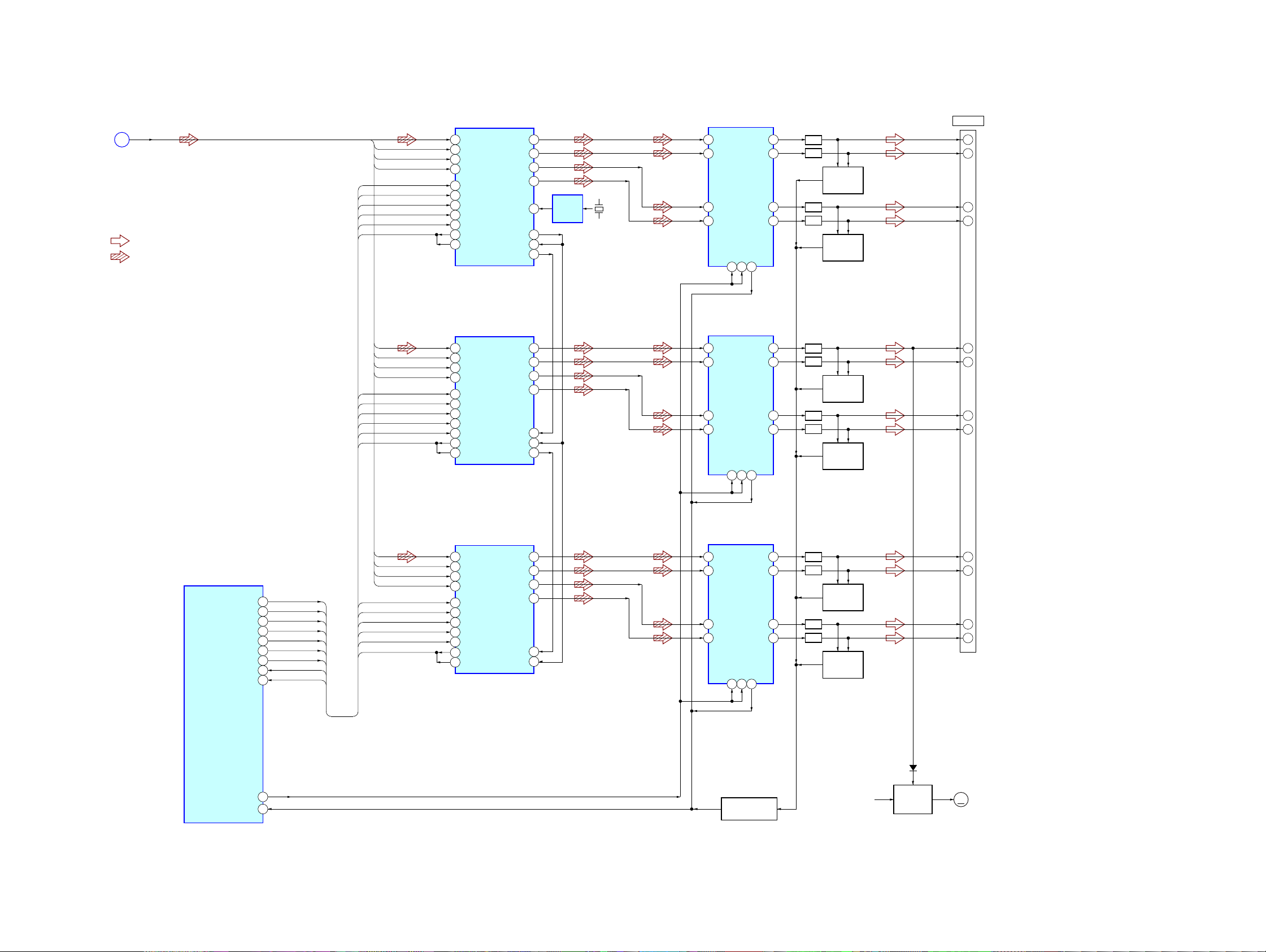
6-2. BLOCK DIAGRAM – HDMI Section (US and Canadian models) –
HCD-X1
DQ0 – DQ15
SD-RAM
IC509
A0 – A11
YUV0
YUV1
YUV2
YUV3
YUV4
YUV5
YUV6
YUV7
HSYNC
VSYNC
VCLK
2, 3, 5, 6, 8, 9,
11, 12, 39, 40, 42,
43, 45, 46, 48, 49
21 – 24,
27 – 32, 20, 19
DQMU
LEVEL SHIFT
IC5401
PROGRESSIVE SCAN CONVERTER
131, 129, 124, 122, 118,
116, 112, 110, 111, 113, 117,
119, 123, 125, 130, 132
88, 86, 82, 80,
81, 83, 87, 89,
95, 97, 94, 96
103
35
14
36
17
16
15
MCLKCLK
101
DQMDQML
100
RASRAS
102
CASCAS
104
WEWE
7
PI2
8
PI3
9
PI4
10
PI5
11
PI6
12
PI7
13
PI8
14
PI9
15
NHSI
16
NVSI
2
CLKI
IC503
MD0 – MD15
MA0 – MA11
53 – 55,
58 – 62
2 – 9,
12, 13
14 – 18,
26 – 30
SDA
BUFFER
SCL
IC111
XADRST
PO0 – PO9
YO0 – YO9
CO0 – CO9
SDA
SCL
136
135
33 – 28,
25 – 22
52 – 48,
45 – 41
56 – 60,
63 – 67
CLKO
137
40
SRN
21
SDA
22
SCL
33
RESET
32
CLKIN
63
CLKIN_2
32 – 39,
42, 43
20,
22 – 30
19 – 17,
15 – 12,
9 – 7
117
DCLK
VIDEO ENCODER
IC506
S (2) – S (9)
P_Y (0) – P_Y (9)
P_C (0) – P_C (9)
PIXEL RESOLUTION CONVERTER
DI0 – DI9
DY0 – DY9
DC0 – DC9
SDA50SCL
49
IC507
QR2 – QR9
QG2 – QG9
QB2 – QB9
NRST
52
RSET1
Y/G
CB/R
CR/B
RSET2
V
Y
C
86 – 90,
93 – 95
74, 75,
77 – 80,
82, 83
62 – 69
47
44
43
42
39
38
37
35
98
99
97
96
RV501
COMPOSITE
VIDEO OUT LEVEL
CVBS
RV502
COMPONENT
VIDEO OUT LEVEL
ASDATA4
ASDATA0
ASDATA1
ASDATA2
SPDIF
ACLK
ABCK
ALRCK
• SIGNAL PATH
CVBS, C, Y, R, G, B
(Page 22)
IC602
D16 – D23
D8 – D15
D7 – D0
C
TX2+
36
TX2–
35
TX1+
33
TX1–
32
TX0+
30
TX0–
29
TXC+
27
TXC–
26
LEVEL
HPD
SHIFT
18 19
IC603
Y
C
G
B
R
HDMI PANELLINK CINEMA TRANSMITTER
56 – 49
67,
65 – 61,
58, 57
79 – 75,
70 – 67
80
DEQDE
66
IDCKQCLK
1
HSYNCQH
2
VSYNCQV
10
SD0
9
SD1
8
SD2
7
SD3
5
SPDIF
6
MCLK
12
SCK
11
WS
: AUDIO (DIGITAL)
: VIDEO
DATA2+
DATA2–
DATA1+
DATA1–
DATA0+
DATA0–
CLOCK+
CLOCK–
SCL (5V)
SDA (5V)
HOT PLUG DET
CN601
HDMI OUT
1
3
4
6
7
9
10
11
15
16
HCD-X1
(Page 22)
B
HDMI BUS
SMSDI
SMSDO
SMSCK
SMSCS
XSMRST
LEVEL
SHIFT
IC608
52
53
51
14
19
SMSDO
SII
SMSDI
XSMCS
XRST
LEVEL
SHIFT
Q602
26
SDA1
RESET
SCL0
17
16
INT
42
35
XTXINT
XTXRST
61
62
SCL
SDA
CSDA43CSCL
44
LEVEL
SHIFT
Q601
X601
8MHz
27
SCL1
36
XIPRST
22
23
X0
X1
HDMI CONTROLLER
IC601
37
XSCRST
31
32
SDA0
2323
Page 24
HCD-X1
6-3. BLOCK DIAGRAM – MAIN Section –
J901
TV
ANTENNA
L
R
L
R
L
R
TV
D
AV0, AV1
E
DIGITAL AUDIO BUS
A
FM 75Ω
COAXIAL
AM
VIDEO 1/
SAT 1
AUDIO IN
VIDEO 2/
SAT 2
AUDIO IN
AUDIO IN
(US, Canadian, Singapore)
(Page 22)
(AEP, UK, Russian)
(Page 22)
(Page 22)
• R-CH is omitted due to same as L-CH.
• SIGNAL PATH
: AUDIO (ANALOG)
: AUDIO (DIGITAL)
R-CH
R-CH
R-CH
TUNER UNIT
L-CH
R-CH
DI
DO
CLK
CE
TUNED
RDS-DATA
RDS-CLK
(AEP, UK, Russian)
ANALOG AUDIO SELECT
Q653 Q654
7
5
8
10
9
11
3
2
1
11 X3
15 X2
14 X1
12 X0
R-CH
B
9
AV1
IC511
13X
A
10
AV0
80 PLL-DI
78 PLL-DO
77 PLL-CLK
79 PLL-CE
85 TUNED
76 RDS-DATA
75 RDS-CLK
MUTING
Q651
MUTING
CONTROL
Q655, 656
73
ATT
LINE AMP
IC512
R-CH
DIGITAL
OUT
OPTICAL
VIDEO 1/SAT 1
DIGITAL IN
OPTICAL
VIDEO 1/SAT 1
DIGITAL IN
COAXIAL
VIDEO 2/SAT 2
DIGITAL IN
COAXIAL
TV
DIGITAL IN
COAXIAL
DIGITAL INPUT
X501
5MHz
15
XIN
OPTICAL
TRANSCEIVER
IC504
OPTICAL
RECEIVER
IC503
J501
S501
SELECTOR
13
XOUT
WAVE
SHAPER
IC510
OPTICAL
COAXIAL
DIGITAL AUDIO SELECT
IC509
15 D4
4D0
14 D5
3D1
13 D6
2D2
C
SW +3.3V
SYSTEM
CONTROLLER
IC501 (2/4)
AV1
A/D CONVERTER
IC513
PDWN
7
72
AD_RST
12DOUT
ASDATA0
ABCK
ALRCK
ACLK
ASDATA1
ASDATA2
DATA SELECT
IC514
11 3A
10 3B
21A
31B
52A
62B
14 4A
13 4B
A/B
1
38
SEL1FS
DSP
IC506
SDO1 AMP BUS
SDO2
SDO3
BCK
LRCK
MCK
S-RAM
IC507
D0 – D15
7 – 10, 13 – 16,
29 – 32, 35 – 38
A0 – A15
5 – 1, 44 – 42,
27 – 24, 21 – 18
17 WE
6CS
F
(Page 25)
MCLK112MCLK2
9
X601
13.9MHz
DSP_BST
23SDO1
24SDO2
25SDO3
20BCKO
19LRCKO
14SCKOUT
108, 107, 105 – 102,
99, 98, 80 – 77, 75 – 72
85 – 82, 66 – 64
112, 110 , 109, 97 – 92,
45SWO
44CSO
18 SDI1
69 GP8
93Y
41Y
72Y
124Y
BST
HDOUT
HCS
HACN
GP9
GP12
PM
XRST
HCS
HDOUT
6
61
DSP_DOUT
30
17 BCKI1
29
15 LRCKI1
28
22
114
115
33 HDIN
34 HCLK
59 EXLOCK
56 BST
35 HDOUT
36 HCS
32 HACN
68 GP9
37 GP12
113 PM
2 XRST
GP9
HACN
58
59
DSP_HCE
DSP_ACK
SDI2
BCKI2
LRCKI2
KFSIO
SDI3
SDI4
PM
GP12
71
65
DSP_GP9
DSP_SKIP
XRST
60
63
DSP_PM
DSP_XRST
D0 – D15
A0 – A15
BST
1
LIN
16DATAO
24AUDIO
14BCK
15LRCK
13CKOUT
12.288MHz
X701
2RIN
18
DIR ZERO
BCK10LRCK15SCKI
11
IC521
R-CH
DIGITAL AUDIO
INTERFACE RECEIVER
IC505
2 SPDIF
SPDIF
4DIN1
3DIN0
DO
36DI35
70
5
DIR HDOUT
CL
37CE38
25
7
67
19
DIR HCE
COM_CLK
COM_DATA
XOUT 21
XIN 22
XSTATE
CSFLAG
XMODE
17
34
48
68
69
66
DIR RST
DIR XSTATE
DIR_CSFLAG
ERROR
DIR RERR
5Y
11A10B9
AV0
HCD-X1
2424
Page 25
6-4. BLOCK DIAGRAM – AMP Section –
HCD-X1
(Page 24)
F
AMP BUS
• R-CH is omitted due to same as L-CH.
• SIGNAL PATH
: AUDIO (ANALOG)
: AUDIO (DIGITAL)
SDO1
MCK
BCK
LRCK
SCDT
SHIFT
LATCH1
INIT
SOFTMUTE
OVF1
SDO3
MCK
BCK
LRCK
SCDT
SHIFT
LATCH3
INIT
SOFTMUTE
OVF2
STREAM PROCESSOR
IC231
31
DATA
36
XFSIIN
30
BCK
29
LRCK
21
SCDT
22
SCSHIFT
23
SCLATCH
27
INIT
19
SOFTMUTE
24
OVF FLAGR
25
FLAGL OVF
STREAM PROCESSOR
IC232
31
DATA
36
XFSIIN
30
BCK
29
LRCK
21
SCDT
22
SCSHIFT
23
SCLATCH
27
INIT
19
SOFTMUTE
24
OVF FLAGR
25
FLAGL OVF
OUTL1
OUTL2
OUTR1
OUTR2
XFSOIN
FSOCKO
FSOI
XFSOOUT
OUTL1
OUTL2
OUTR1
OUTR2
XFSOIN
FSOI
XFSOOUT
SW+
SW
SW+
SW
CN300
SPEAKER
–
–
–
–
13
15
14
12
5
7
9
11
DIGITAL POWER AMP
IC301
11
9
6
4
OSC
BUFFER
48
IC271
X271
37
38
14
11
9
6
4
48
38
14
49.152MHz
4
PWM_A
6
PWM_B
14
PWM_C
16
PWM_D
/RST_AB
5
DIGITAL POWER AMP
4
PWM_A
6
PWM_B
14
PWM_C
16
PWM_D
/RST_AB
5
15 3
IC302
15 3
OUT_A
OUT_B
OUT_C
OUT_D
/RST_CD
/SD
OUT_A
OUT_B
OUT_C
OUT_D
/RST_CD
/SD
33
30
25
22
33
30
25
22
LPF
LPF
LPF
LPF
LPF
LPF
LPF
LPF
OVER LOAD
DETECT
Q304, 310
OVER LOAD
DETECT
Q301, 307
OVER LOAD
DETECT
Q305, 311
OVER LOAD
DETECT
Q302, 308
FRONT LCH+
FRONT LCH
FRONT RCH+
FRONT RCH
SYSTEM CONTROLLER
IC501 (3/4)
DAMP SCDT
DAMP SHIFT
DAMP LATCH1
DAMP LATCH2
DAMP LATCH3
DAMP INIT
DAMP SOFT MUTE
OVERFLOW1
OVERFLOW2
DRIVE_RST
DRIVE_OCP
STREAM PROCESSOR
IC233
SDO2
MCK
BCK
LRCK
1
2
51
52
53
54
55
49
50
47
48
SCDT
SHIFT
LATCH1
LATCH2
LATCH3
INIT
SOFTMUTE
OVF1
OVF2
SCDT
SHIFT
LATCH2
INIT
SOFTMUTE
OVF1
31
36
30
29
21
22
23
27
19
24
25
DATA
XFSIIN
BCK
LRCK
SCDT
SCSHIFT
SCLATCH
INIT
SOFTMUTE
OVF FLAGR
FLAGL OVF
OUTL1
OUTL2
OUTR1
OUTR2
XFSOIN
FSOI
11
9
6
4
48
38
DIGITAL POWER AMP
IC303
4
PWM_A
OUT_A
6
14
16
PWM_B
PWM_C
PWM_D
/RST_CD
/RST_AB
15 3
5
Q313
PROTECT DETECT
OUT_B
OUT_C
OUT_D
/SD
D452
FAN MOTOR
DRIVE
Q451 – 453
REAR LCH+
REAR LCH
REAR RCH+
REAR RCH
4
–
2
1
–
3
M450
M
(FAN)
33
30
25
22
LPF
LPF
LPF
LPF
OVER LOAD
DETECT
Q306, 312
OVER LOAD
DETECT
Q303, 309
AMP +12V
HCD-X1
2525
Page 26
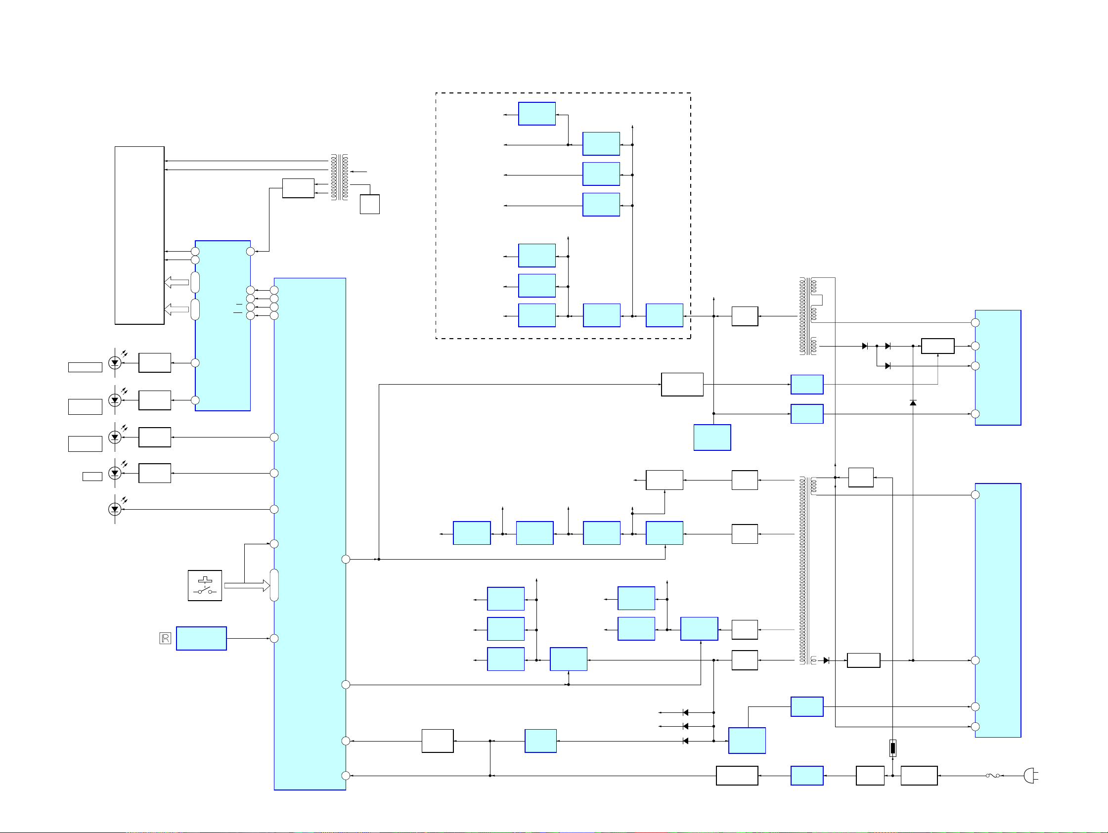
HCD-X1
6-5. BLOCK DIAGRAM – PANEL/POWER SUPPLY Section –
D809
2CH STEREO
D808
WIDE
SURROUND
D807
FOCUS
SURROUND
D806
AUTO
D841
(STANDBY)
FLUORESCENT
INDICATOR TUBE
FL841
LED DRIVE
Q814
LED DRIVE
Q813
LED DRIVE
Q812
LED DRIVE
Q811
S801, 802
S804 – 806
S841, 842
FL DRIVER
IC842
4
AD1
3
AD2
5 – 39
S1 – S35
40 – 50
G1 – G11
2
P2
1
P1
REMOTE CONTROL
RECEIVER
IC841
VFL
DAT
CLK
RST
HDMI
+1.8V
DC/DC
CONVERTER
T841
SW +5V
RECT
D842 – 845
56
27
63
62
61
CS
60
FL_D_OUT
24
FL_CLK
28
FL_CS
41
FL_RESET
23
LED1
22
LED0
26
STBY_LED
74
KEY INY
KEY0 – KEY2
97, 95, 94
4
SIRCS_IN
SYSTEM
CONTROLLER
IC501 (4/4)
OSC
Q841
PIXEL RESOLUTION
SCAN CONVETRTER
D +3.3V
44P_CONT2
RF +1.8V
AMP +1.8V
DSP +1.8V
40P_CONT1
P +3.3V
A +3.3V
VIDEO ENCODER
CONVERTER
PROGRESSIVE
+3.3V
REGULATOR
IC518
HDMI
HDMI
HDMI
+5V
+2.5V
+2.5V
+2.5V
+1.8V
REGULATOR
IC106
+1.8V
REGULATOR
IC201
+1.8V
REGULATOR
IC515
+1.8V
REGULATOR
IC604
+2.5V
REGULATOR
IC508
+2.5V
REGULATOR
IC505
+2.5V
REGULATOR
IC501
+5V
REGULATOR
IC519
SW +3.3V
REGULATOR
REGULATOR
REGULATOR
HDMI
SW +3.3V
REGULATOR
D +9VD +5V
REGULATOR
SERVO DSP +3.3V
RF +3.3V
+3.3V
REGULATOR
IC11
SW +5.2V
+3.3V
IC607
+3.3V
IC606
+5V
IC605
+3.3V
IC16
SW +9V
+9V
IC520
REGULATOR
REGULATOR
HDMI
D +12V
+3.3V
IC105
+3.3V
IC107
(US, Canadian)
+5.2V
REGULATOR
IC15
POWER ON/OFF
CONTROL
Q143, 147
B+ SWITCH
Q11
+12V
REGULATOR
IC12
SW +5V
AMP +27V
SHUNT
REGULATOR
IC131
+5V
REGULATOR
IC13
RECT
D131
RECT
D141
RECT
D144
RECT
D142
RECT
D143
MAIN POWER
TRANSFORMER
T101
ISOLATOR
PC102
ISOLATOR
PC101
SUB POWER
TRANSFORMER
T102
D122
D105
RECT
D101
SWITCHING
Q121
D108
D106, 107
D110
SWITCHING
Q101
POWER CONTROL
IC101
3
D
4
VCC
1
OCP/SYNC
5
FB/OLP
POWER CONTROL
IC121
1
DRAIN
4
VCC
HCD-X1
RESET
SYSTEM +3.3V
12
20AC_CUT
RESET
SWITCH
Q502
VOLTAGE
DETECT
IC502
E +3.3V
D501
D504
D502
SHUNT
REGULATOR
IC151
AC DETECT
Q161, 162
ISOLATOR
PC104
ISOLATOR
PC103
TH101
RECT
D103, 104
LINE FILTER
LF101
6
FB/OLP
8
STARTUP
F101
(AC IN)
2626
Page 27
HCD-X1
d
• Note for Printed Wiring Boards and Schematic Diagrams
Note on Printed Wiring Board:
• X : parts extracted from the component side.
• Y : parts extracted from the conductor side.
f
•
• : Pattern from the side which enables seeing.
(The other layers' patterns are not indicated.)
Caution:
Pattern face side: Parts on the pattern face side seen from
(Conductor Side) the pattern face are indicated.
Parts face side: Parts on the parts face side seen from
(Component Side) the parts face are indicated.
• DMB10 and MIB01 boards are multi-layer printed board.
• Indication of transistor
: internal component.
However, the patterns of intermediate layers have not been
included in diagrams.
C
B
Q
B
E
Q
CE
These are omitted.
These are omitted.
Note on Schematic Diagram:
• All capacitors are in µF unless otherwise noted. (p: pF)
50 WV or less are not indicated except for electrolytics
and tantalums.
• All resistors are in Ω and 1/
specified.
f : internal component.
•
• 2 : nonflammable resistor.
• 5 : fusible resistor.
• C : panel designation.
Note:
The components identified by mark 0 or dotted
line with mark 0 are critical for safety.
Replace only with part
number specified.
• A : B+ Line.
• B : B– Line.
• C : adjustment for repair.
• Voltages and waveforms are dc with respect to ground
under no-signal conditions.
– DMB10, MIB01 and IO Boards –
no mark : DVD PLAY
∗ : Impossible to measure
– Other Boards –
no mark : TUNER
(): DVD PLAY
∗ : Impossible to measure
• Voltages are taken with a VOM (Input impedance 10 MΩ).
Voltage var iations may be noted due to normal production tolerances.
• Waveforms are taken with a oscilloscope.
Voltage var iations may be noted due to normal production tolerances.
• Circled numbers refer to waveforms.
• Signal path.
F : AUDIO (ANALOG)
J : AUDIO (DIGITAL)
E : VIDEO
• Abbreviation
CND : Canadian model
RU : Russian model
SP : Singapore model
4
W or less unless otherwise
Note:
Les composants identifiés par
une marque 0 sont critiques
pour la sécurité.
Ne les remplacer que par une
pièce portant le numéro
spécifié.
• Circuit Boards Location
DMB10 board
FL board
MS-203 board
TUNER UNIT
SWITCH board
SCART board
(AEP, UK and Russian models)
MIB01 board
(US, Canadian models)
IO board
MAIN boar
POWER-AMP board
HCD-X1
2727
Page 28
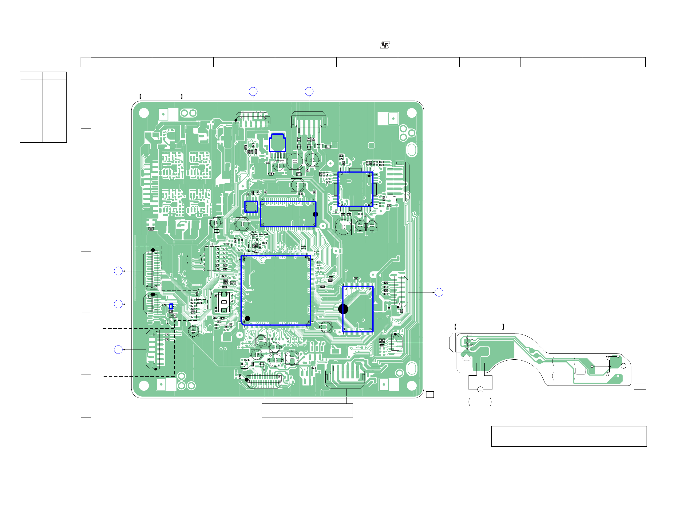
HCD-X1
• Semiconductor
Location
Ref. No. Location
D1001 B-3
IC101 D-5
IC102 D-4
IC103 C-3
IC104 C-4
IC106 B-4
IC201 B-5
IC4801 D-2
Q103 E-3
6-6. PRINTED WIRING BOARDS – DMB10 Section (1/2) –
1 2 3 4 5 6 7 8 9
A
DMB10 BOARD (COMPONENT SIDE)
R4503
B
C167
IC103
C
C308
(US, CND)
E
MIB01
D
BOARD
CN5401
(Page 34)
F
MIB01
BOARD
CN5201
(Page 34)
E
D
IO
BOARD
CN902
(Page 42)
CN4801
IC4801
R4805
12
C4801
11
C4803
CN4802
FL4801
R4706
R4705
CN301
(EXCEPT US, CND)
R1519
R1518
4
R1520
135
R1528
R1522
R1523
EXCEPT
US, CND
C150
C178
EXCEPT
US, CND
R1543
FL107
R189
R190
R192
R195
R197
R1102
C145
C137
C135
(US, CND)
R1511
R155
R153
R144
C153
C152
C138
R1521
X101
C132
R136
C177
R1101
R1512
R1513
R1514
R1515
R1516
R1517
R1550
C142
Q103
R1553
R142
256
C133
C170
R1549
R1168
C118
R117
E
R1105
192
193
1
R1129
F
• See page 27 for Circuit Boards Location. : Uses unleaded solder.
CN401
(Page 47)(Page 46)
MAIN BOARD
CN508
MAIN BOARD
C B
CN504
CN4501
IC106
R4504
R4505
R193
R1508
R116
R4506
R4507
C189
R191
R1510
R1108
R1107
C117
C187
R1109
C101
CN101
15
D1001
C190
C181
IC104
(US, CND)
R1111
(US, CND)
IC102
C116
C119
C112
FL101
FB402
FL401
C402
FB404
C180
129
R234
C105
OPTICAL PICK-UP BLOCK
(KHM-310CAA)
RB108
FB403
FL403
64
C403
FB406
R101
FL402
RB107
128
RB112
65
FB401
R219
R227
C179
R152
R228
RB113
C129
C210
R1557
R216
R224
R161
FB405
R210
13
24
C223
C208
C222
12
25
C217
CN201
IC201
C219
C221
C102
IC101
C218
36
C206
1
R215
C224
C220
C205
R214
R208
48
37
FB114
FB113
R209
FB115
C226
R243
FB112
R233
C215
R107
C225
10
C108
5
CN202
11
CN106
4
CN105
R1545
1-864-397-
(NC)
A
MAIN
BOARD
CN503
(Page 46)
11
MS-203 BOARD
1
2
CN001
5
4
MM
M301
DISC TRAY
OPEN/CLOSE
S001-1
DISC TRAY
OPEN DETECT
S001-2
DISC TRAY
CLOSE DETECT
S001
–1
–2
1-861-327-
12, 21
HCD-X1
New part of EEPROM (IC103) on the DMB10 board cannot be used.
Therefore, if the mounted DMB10 board is replaced, exchange new
EEPROM with that used before the replacement.
2828
Page 29
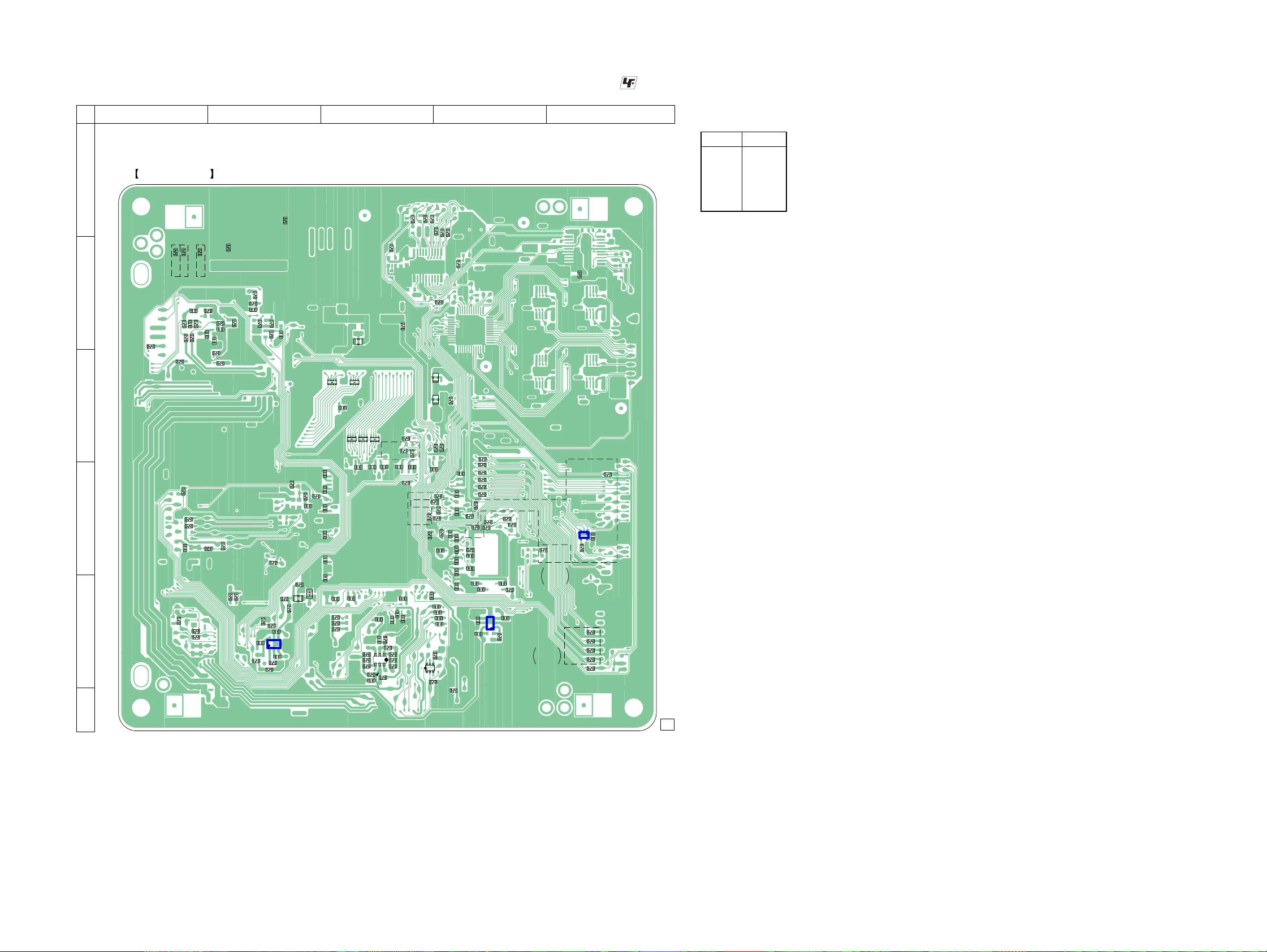
HCD-X1
6-7. PRINTED WIRING BOARD – DMB10 Section (2/2) –
1 2 3 4 5
A
B
C
DMB10 BOARD (CONDUCTOR SIDE)
(AEP, UK, RU)
R5014
R226
C212
R212
R221
R232
C214
R230
R206
C209
R5007
R207
C203
R204
R205
R213
R222
C213
R1110
(SP)
R220
R231
R5017
C211
R5016
(US, CND)
C233
R223
R225
R5010
RB105
C191
FL108
RB106
• See page 27 for Circuit Boards Location. : Uses unleaded solder.
• Semiconductor
Ref. No. Location
IC105 E-2
IC107 E-4
IC4802 D-5
Q101 E-3
Q102 E-3
R4508
R1134
R4512
R4516
R4511
R4510
R4515
R4501
FL104
FL106
R4514
R4502
R3610
R4513
Location
RB111
RB104
RB103
(US, CND)
C175
C131
C164
C162
C128
C158
C155
C144
C136
C127
R121
R120
R118
C176
R110
C106
R1546
R1502
C109
R239
R1151
R1152
FB111
R2505
R237
R1150
R106
C188
R105
R247
R238
R104
R196
R236
5
1
R246
D
E
R164
R169
FL105
R1133
C182
4
IC105
3
C184
R187
R1504
C160
R135
R134
R133
C174
(US, CND)
C196
C113
2C2B
1E
2E1B1C
R1506
C126
Q102
C173
R123
R124
R109
R1555
R1505
R1554
C125
C115
R113
R112
R115
C172
R1552
R1530
C114
C148
2S2G
2D1G
C171
R4801
R1531
R1540
C124
R111
R108
R1104
R143
C120
1D
Q101
1S
C163
C123
C122
C121
R1103
C159
R1551
C156
C149
C140
C130
R114
C161
R160
C154
C146
C193
R4803
R141
C151
C147
C143
IC107
C195
R4802
R1548
C139
4
5
R1125
R1124
R1123
R1122
R1121
R1120
R1547
3
1
C141
R138
C192
R126
R151
R146
IC4802
R1542
EXCEPT
US, CND
EXCEPT
US, CND
4
R4806
R4704
R4703
R4702
R4701
R308
R4804
13
5
(US, CND)
C4802
F
1-864-397-
11
HCD-X1
2929
Page 30
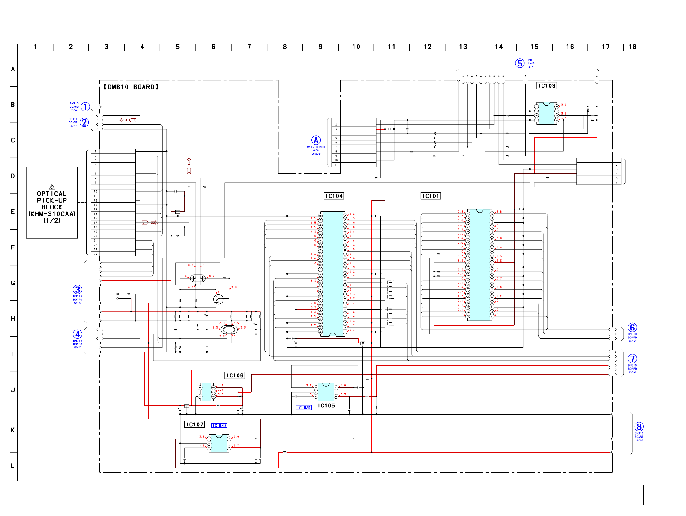
HCD-X1
Ver. 1.1
6-8. SCHEMATIC DIAGRAM – DMB10 Section (1/4) –
(1/4)
(Page 32)
MSW
A5
A4
A3
REGO1
OCSW1
RF+3.3V
REGO2
RF+3.3V
V2REFO
TRK-
TRK+
FCS+
FCS-
RF1.8
IOP
A2
CN101
24P
GND (LD)
LD (650)
NC
NC
PD
LD (780)
VR (650)
VR (780)
NC
VOE/E+G
VCC
VC
GND (PDIC)
VOF/F+H
VOB/B
VOA/A
RF
(LO:DVD.HI:CD)MSW
VOD/D
VOC/C
TRK-
TRK+
FCS+
FCS-
CL107
CL106
A6
A7
A8
DVD_LD
CD_LD
VOE
VOF
VOB
VOA
VOD
VOC
TRK-
TRK+
FCS+
FCS-
TRK-
TRK+
FCS+
FCS-
R107
10k
(Page 32)
(Page 31)
(Page 32)
• See page 64 for IC Block Diagrams.
R101
C101
0.01
FL101
R116
1k
Q101
UM6K1N-TN
R108
1M
R112 R113 R118 R120R115
22 22 22 2222
R109
0
DVD_LD
CD_LD
R114
100k
R1129
100k
FL107
C178
47
4V
100
SS
-1 -2
R111
100
R110
47k
IC106
PQ018EN01ZP
VADJ
GND
Q101,103
R117
VOLUME CONTROL
47k
Q103
RT1N241C-TP-1
R121 R124
Q102
QST8TR
CONTROL
22 47k
C112
47
6.3V
D1001
RB501V-40TE-17
C187
47
4V
C105
47
6.3V
-1 -2
R1134
0
AUTOMATIC POWER
+1.8V REGULTOR
C189
0.33
C106
0.01
VO
VB
VIN
(Page 32)
Q
E
R
M
CN106
11P
GND/OCSW1
SYSRST
3.3VMNT
XIFCS
IFBSY
SIO
SOO
MREQ
LDQM
VDDQ
VDDQ
SCO
GND
OPEN
R1545
0
C181
R187
R1133
0.1
C180
0.1
RB106
47
RB105
47
C179
0.1
0
0
R169
10k
VDD
A3
A2
A1
A0
A10
BA1
BA0
/CS
/RAS
/CAS
/WE
VDD
DQ7
VSSQ
DQ6
DQ5
DQ4
DQ3
VSSQ
DQ2
DQ1
DQ0
VDD
FL108
C188
0.22
C182
0.22
(Page 51)
SD-RAM FLASH ROM
IC104
HY57V64162
0HGTP-HDR
RA4
RA5
RA6
RA7
RA8
RA9
RA11
DRCKE
DRCLK
DQM1
RD8
RD9
RD10
RD11
RD12
RD13
RD14
RD15
C113
0.01
C191
0.1
C190
47
6.3V
C184
0.01
VSS
A4
A5
A6
A7
A8
A9
A11
NC
CKE
CLK
UDQM
NC
VSS
DQ8
VDDQ
DQ9
DQ19
VSSQ
DQ11
DQ12
VDDQ
DQ13
DQ14
VSSQ
DQ15
VSS
IC105
TK11133CSCL-G
CONT
VIN
GND
NOISE
VOUT
+3.3V REGULTOR
C109
C108
0.001
0.001
R1502
RA3
RA2
RA1
RA0
RA10
BA1
BA0
RCS
RAS
CAS
RWE
DQM0
RD7
RD6
RD5
RD4
RD3
RD2
RD1
RD0
FB111
FB112
FB113
FB114
0
FB115
0
MX29LV320ABTC65-0HD1-0503UC(US,CND)
MX29LV320ABTC65-0ED2-0503CE(AEP,UK,RU)
0
R104
MX29LV320ABTC65-0ED2-0503GA(SP)
A16
A15
A14
A13
A12
A11
A10
A9
A20
A21
R105
10k
10k
A19
R106
A18
A8
A7
A6
A5
A4
A3
A2
A18
A22
A19
A16
A17
IC101
A16
A15
A14
BYTE
A13
VSS
A12
DQ15/A-1
A11
DQ7
A10
DQ14
A9
DQ6
A8
DQ13
A19
DQ5
N.C.
DQ12
DQ4
WE
VCC
RESET
DQ11
N.C.
DQ3
N.C.
DQ10
RY/BY
DQ2
A18
DQ9
A17
DQ1
A7
DQ8
A6
DQ0
A5
A4
A3
VSS
A2
A1
A24
A23
A26
A20
A21
R1546 R193
3.3k 1k
OE
CE
A0
R1150
R1152
R1151
A25
EEPROM
IC103
BR24L64F-WE2
(NOT SUPPLIED)
A0
VCC
A1
A2
SCL
GND
SDA
3.3k
3.3k
3.3k
2.7k
R1110
C102
1
XROMCS
A17
A0
HD7
HD6
HD5
HD4
HD3
HD2
HD1
HD0
XRD
A1
XWR
A27
C167
0.01
R191
1k
CN105
6P
TXD
RXD
GND
+3.3V
V2REFO
RFMON
(NC)
A13
A14
A15
(Page 32)
A28
A29
A30
A31
A32
A33
(Page 32)
GND
HCD-X1
+3.3V REGULTOR
IC107
TK11133CSCL-G
CONT
GND
NOISE
VIN
VOUT
C193 C195C192
0.22 0.220.01
R126
0
SW+5V
SW+3.3V
(Page
33)
New part of EEPROM (IC103) on the DMB10 board cannot be used.
Therefore, if the mounted DMB10 board is replaced, exchange new
3030
EEPROM with that used before the replacement.
Page 31

6-9. SCHEMATIC DIAGRAM – DMB10 Section (2/4) –
(2/4)
HCD-X1
R223
100k
(Page 32)
IOPMON
VREFO
R225
100k
CN201
CN202
RF+3.3V
IOP
FCS-
FCS+
TRK+
TRK-
REGO2
REGO1
OCSW1
6P
LIMITSW
CKSW
OCSW
(Page 30)
(Page 32)
5P
CN001
5P
S001
S001-1
(DISC TRAY OPEN DETECT)
S001-2
(DISC TRAY CLOSE DETECT)
M301
(DISC TRAY OPEN/CLOSE)
SPFG
FOO
TRO
FMO
C233
0.0047
R212
10k
SPINDLE/SLED/LOADING MOTOR DRIVER
R208
33k
C205 R214
220p 15k
R206
10k
C206 R215
R209
220p 12k
33k
R204
R207 C203
1.2k
2.7k 0.01
R205
10k
R210 C208
47k 0.01
R213
6.8k
FOCUS/TRACKING COIL DRIVER,
R216
12k
33
0.0
9
0
2
C
R221
56k
R220
10k
3
3
.0
0
11
2
C
R226
56k
0.001
R231 R232
R230
15k 18k
82k
C212
0.01
C214
IC201
FAN8036L
R234
10k
R233
33k
C215
0.01
C218 C220
10
16V
FCS-
FCS+
TRK+
TRK-
C224
0.01
C219
0.01
10
16V
C221
0.1
C222
0.1
C223
0.1
SL-
SL+
SP-
SP+
FCS-
FCS+
TRK+
TRK-
SP-
SP+
SL-
SL+
R247
1k
R246
4.7k
R238
47k
C225 R236
R2505
0.001 1k
0
C226
R239
0.001
47k
R237
1k
R243
100
SP-
SP+
LIMIT
(GND)LIMIT
SL-
SL+
OCSW1
CKSW1
GND
LDM-
LDM+
HCD-X1
(Page 32)
TROPENPWM
MUTE123
TSD_M
MUTE
DMO
FWD
REV
R219
27k
R222
33k
R227
0
R228
0
R224
10k
C210
0.01
C213
0.01
C217
47
16V
GND
SW+3.3V
SW+9V
SW+5V
MTR_GND
(Page 33)
3131
Page 32

HCD-X1
6-10. SCHEMATIC DIAGRAM – DMB10 Section (3/4) – • See page 61 for Waveforms. • See page 73 for IC Pin Function Description.
(Page 33)
(Page 30)
(Page 30)
(Page 31)
TROPENPWM
RF+3.3V
IOPMON
(EXCEPT US,CND)
R1120
(3/4)
A_BUS
ABCK
SPDIF
ASDATA4
47
100
R146
R143
12p
12p
0.1
15k
0.1
C130
R136
C132
A2
A3
A4
A5
RF1.8
A6
A7
A8
V2REFO
VREFO
16V
0.1
10
C114
C117
DMO
FMO
TRO
FOO
SPFG
VOA
VOB
VOC
VOD
VOE
VOF
16V
16V
0.1
10
0.1
10
C115
C118
C116
C119
A2
A3
A4
A5
A6
A7
A8
A18
A19
C120
1
C121
1
C122
1
C123
1
C124
1
R123
0
C125
0.1
C126
0.1
C196
0.0047
R133
3.3k
R134
3.3k
R135
3.3k
C127
0.01
C128
0.0015
0.033
0.1
22p
0.1
0.1
0.1
1
100k
C135
C137
C139
R138
C133 C147 C148
0.1 0.047 0.047
0.001
C138
0.1
C140
C141
C143
C145
C146
0.1
C142
16V
0.1
10
X101
27MHz
C149
C150
C151
0.001
750k
R141
C152
C153
100k
R142
0
470
R144
R1168
0.1
C154
RF AMP, SERVO DSP,
MPEG DECODER
IC102
CXD9804R
0.01
4.7k
C156
R1547
ACLK
ALRCK
ASDATA1
ASDATA2
ASDATA0
0
47
R151
4.7k
R1540
0
47
47
47
R1531
R1530
R153
R155
R160
4.7k
4.7k
R1550
4.7k
4.7k
R1549
R1548
R1551
0
R1542
ND)
,C
(US
1.8k
0
R1552
R1528
R195
150
R1102
150
150
R192
150
R190
R197
0.01
C161
150
R189
150
(EXCEPT US,CND)
0.01
0.01
C163
(EXCEPT US,CND)
C159
R1543
10k
∗
R1101
560(US,CND)
2.2K(EXCEPT US,CND)
(US,CND)
R1553
0
R1508
R1111
0
R196
0
R1101
∗
C170
0.01
R1103
10k
C171
0.01
R1105
10k
R1107
0
ICT130
C172
0.01
R1108
10k
R1554
4.7k
R1555
C173
4.7k
0.01
C174
0.01
C175
0.01
C176
0.01
0
R1121
0
R1122
0
R1123
0
R1124
0
R1125
0
R1523
0
R1522
0
R1521
1k
R1520
33
R1519
33
R1518
R1517
R1516
R1515
R1514
R1513
R1512
R1511
R1510
0
(US,CND)
R1104
10k
R1109
0
R1506
0
R1505
10k
(US,CND)
RA4
RA5
RA6
RA7
RA8
RA9
RA11
DRCKE
DRCLK
RB104
0
RA3
RA2
RA1
RB103
0
RA0
RA10
BA1
BA0
RB111
0
RCS
RAS
CAS
RWE
DQM1
RB108
22
RD8
RD9
RD10
RD11
RD12
RD13
RD14
RD15
RB107
22
CR/R
CB/B
Y/G
V
C
Y
XSMCS
SMSDO
SMSCK
SMSDI
HSYNC
VSYNC
YUV7
YUV6
YUV5
YUV4
YUV3
YUV2
YUV1
YUV0
XADRST
VCLK
XSMRST
MSW
FWD
REV
MUTE123
MUTE
TSD_M
CKSW
OCSW
LIMITSW
WIDE
RGBSEL
A28
A29
A30
A31
(Page 33)
(Page
33)
(Page 30)
(Page 31)
(Page 31)
(Page 33)
HCD-X1
(Page 30)
FL105
(Page 30)
A32
2.2
C131
C129
10
16V
XWR
A13
A14
A15
A16
0.01
C136
A11
A10
A12
A13
A14
A15
0.01
C144
A9
A1
XROMCS
XRD
HD3
HD0
A20
HD1
HD6
HD2
HD5
HD4
HD7
A21
0.01
C155
A0
A17
A16
A17
SDA
SCL
(Page 33)
100
0
100
0.01
R1557
R152
R161
C158
A18
A19
A20
A21
A22
A23
A24
R1504
C160
0.01
RB112
22
R164
100
RD7
DQM0
A25
A26
MREQ
0.01
C162
RB113
22
RD4
RD5
RD6
RD0
RD1
RD2
RD3
(Page 30)
FL106
0.01
C177
47
C164
6.3V
FL104
A27
A33
3232
Page 33

6-11. SCHEMATIC DIAGRAM – DMB10 Section (4/4) –
HCD-X1
(Page 49)
(Page 32)
A_BUS
SW+5V
GND
SW+3.3V
SW+9V
MGND
5P
ABCK
ACLK
FL4801
R4802
R4801
(4/4)
FB402
FB403 FL403
FB401
R5007
0
R5010
0
∗
R4512
0(US,CND)
10(EXCEPT US,CND)
0
0
R4806
56
R4505
R4504
R4503
R4506
R4507
R4508
ASDATA0
ASDATA1
ASDATA2
ABCK
ALRCK
ACLK
SPDIF
C4803
10
C4802
0.01
0
C4801
0.01
0
LEVEL SHIFT
IC4802
SN74LVC1G125DCKR
G
IC4801
SN74LVC1G125DCKR
G
R4502
R4501
V
FL401 FB404
C402
47
16V
FL402CN401
(US,CND)
R5014
0
(AEP,UK,RU)
R5016
0
0
0
0
0
0
0
ASDATA0
ASDATA1
ASDATA2
ASDATA4
ALRCK
SPDIF
R4514
R4515
R4516
R4510
R4511
R4512
R4513
(SP)
R5017
0
0
0
0
0
0
∗
0
R4805
R4803
R308 R3610
CN4802
0
C403
47
6.3V
00
12P
D-GND
ADATA0
ADATA1
ADATA2
ADATA4
ABCK
ALRCK
D-GND
ACLK
D-GND
SPDIF
D-GND
FB406
FB405
D-GND
D1
D2
D3
BCKO
LRCKO
D-GND
MCKO
D-GND
SPDIF
D-GND
CN4501
11P
SW+5V
SW+3.3V
GND
SW+9V
MTR_GND
GND
SW+5V
SW+3.3V
(Page 30)
(Page 48)
(US,CND)
(Page 36)
(Page 31)
(Page 32)
(Page 32)
(US,CND)
(Page 32)
EXCEPT
US,CND
(Page 32)
RGBSEL
HSYNC
VSYNC
XSMCS
SMSCK
SMSDI
SMSDO
XSMRST
XADRST
WIDE
CR/R
CB/B
VCLK
YUV0
YUV1
YUV2
YUV3
YUV4
YUV5
YUV6
YUV7
SDA
SCL
R308
0
R4701
0
R4702
0
R4703
R4704
R4705
R4706
0
0
0
0
R4804
0
Y/G
Y
C
V
RGBSEL
DSEL/DISCXEXT
Cr/R
WIDE
Cb/B
D-GND
Y/G
D-GND
Y
D-GND
C
D-GND
V
D-GND
RGBSEL
DSEL/DISCXEXT
WIDE
D-GND
VCLK
D-GND
YUV0
YUV1
YUV2
YUV3
YUV4
YUV5
YUV6
YUV7
D-GND
HSYNC
VSYNC
D-GND
XSMCS
SMSCK
SMSDI
SMSDO
XSMRST
XADRST
SCL
SDA
D-GND
CN301
CN4801
28P
13P
(Page 41)
(Page 36)
HCD-X1
V
LEVEL SHIFT
3333
Page 34

HCD-X1
• Semiconductor
Location
Ref. No. Location
IC501 D-2
IC503 C-3
IC506 E-5
IC507 C-6
IC508 E-4
IC601 E-8
IC602 C-9
IC603 B-10
IC5401 E-3
6-12. PRINTED WIRING BOARD – MIB01 Board (Component Side) (US and Canadian models) –
1 2 3 4 5 6 7 8 9 10 11
A
B
C
D
E
F
MIB01 BOARD
C524
C508
C503
54
C520
C516
109
C513
C507
C525
IC501
13
C501
C502
IC5401
C5502
R5505
(COMPONENT SIDE)
108
IC503
144
1
C504
R501
C512
R5527
R5525
C562
R5529
R5531
54
13
C5501
R5405
R504
R5407
R5409
R5501
R5504
C5504
CN5401
IC508
C564
C523
135
C552
R526
C505
73
73
C517
72
C519
C536
C539
C541
C540
C543 C544
R527
IC507
116
48
R5309
R5313
C532
C528
64
49
C542
C553
R5101
R5102
R535
37
C506
36
C529
17
C561
4
C535
IC506
32
33
R537
C555
R5303
R5305
R5307
CN5301
• See page 27 for Circuit Boards Location. : Uses unleaded solder.
CN601
HDMI
LF601
IC602
LF602
C604
R1607
OUT
LF603
LF604
C617
C5102
C5105
C5108
R691
R1617
R1618
R551
C545
R515
R516
C534
C547
C533
R536
C557
R632
R631
R633
C558
R630
R626
R617
R629
R607
R659
R624
FL602
R665
R608
FL603
IC601
R605
C601
C614
C615
X601
C602
FL604
R677
FL601
R664
R655
C618
C611
R671
C603
C616
C607
R654
R648
R1616
R693
R692
R687
R689
C619
FL5101
FL5102
C5109
C5106
R694
3
C5103
1
54
C622
R1623
FB5101
FB5102
FB5103
FL5103
CN5201
FL605
C5107
R682
R684
IC603
1
C5101
6
CN5101
H
MAIN
BOARD
NO501
(Page 47)
HCD-X1
G
R5530
R5526
R5528
R5524
DMB10 BOARD
CN4801
(Page 28)
IO BOARD
CN902
(Page 42)
RV501
RV502
DMB10 BOARD
FGE
CN4802
1-865-785-
11
(11)
(Page 28)
3434
Page 35

HCD-X1
6-13. PRINTED WIRING BOARD – MIB01 Board (Conductor Side) (US and Canadian models) –
21 3 4 5 6 7 8 9 10 11
D
A
MIB01 BOARD
B
R1634
R1633
C
IC605
4
C637
6
C641
R1610
E
(CONDUCTOR SIDE)
R681
3
1
R5211
C5204
R5003
R5209
C638
R5207
R675
C608
R627
R5002
C610
R625
C605
R5001
C613
C612
IC606
C609
C606
R673
R603
R602
C626
45
C625
R679
R668
R670
S
R667
C629
C620
Q601
R666
13
4
D
C624
R696
C621
G
R1621
4
6
C628
13
IC604
6
C623
D
Q602
R674
R604
IC607
3
1
R612
R690
C560
R628
R615
IC505
SG
C631
R638
R639
C556
C627
R697
C559
C551
R534
C563
R672
R641
R640
F
R5208
R5204
R5206
R5210
R5202
• See page 27 for Circuit Boards Location. : Uses unleaded solder.
R509
IC509
6
RB5502
R5541
C566
C565
R5551
R5423
R5420
R5539
R5550
R5549
R5419
R5421
R5418
R5540
R5548
R5417
R5537
R5536
R5538
R5547
R5415
R5535
R5416
R5534
R5545
R5546
RB5501
R5411
R5414
R5544
R5412
R5404
R5406
R5408
C527
R524
IC608
C526
C530
C531
R533
R540
C548
R538
R539
C554
R5311
R543
R542
C549
R541
C546
R532
C550
IC111
R559
R5452
13
4
R5453
R5403
R5402
C518
1-865-785-
• Semiconductor
Location
Ref. No. Location
IC111 E-8
IC505 D-6
IC509 B-9
IC604 C-5
IC605 D-2
IC606 B-5
IC607 B-5
IC608 E-6
Q601 D-5
Q602 D-5
11
(11)
HCD-X1
3535
Page 36

HCD-X1
Ver. 1.1
6-14. SCHEMATIC DIAGRAM – MIB01 Board (1/5) (US and Canadian models) –
(1/5)
IC111
(Page 33)
(Page 41)
CN5401
28P
D-GND
SDA
SCL
XADRST
XSMRST
SMSDO
SMSDI
SMSCK
XSMCS
D-GND
VSYNC
HSYNC
D-GND
YUV7
YUV6
YUV5
YUV4
YUV3
YUV2
YUV1
YUV0
D-GND
VCLK
D-GND
WIDE
DSEL/DISCXEXT
RGBSEL
D-GND
CN5301
13P
RGBSEL
DSEL/DISCXEXT
Cr/R
WIDE
Cb/B
D-GND
Y/G
D-GND
Y
D-GND
C
D-GND
V
R5402
R5403
R5404
R5405
R5406
R5407
R5408
R5409
R5411
R5412
R5527
R5528
R5423
R5526
R5529
0
0
0
0
0
0
0
0
0
0
R5525
680
680
R5530
100
R5524
680
680
R5531
R5303
R5305
R5307
R5309
R5311
R5313
XADRST
XSMRST
SMSDO
SMSDI
SMSCK
XSMCS
680
680
VSYN
HSYN
R5452
4.7k
680
680
C5504
0
R5505
680
0
0
0
0
0
0
R5504
R5534
R5535
680
680
680
R5536
R5537
SN74LVC1G125DCKR
µM6K1N-TN
1S 1D
1G 2G
680
680
R5538
LEVEL SHIFT
BUFFER
R5539
IC5401
G
680
R5540
2S2D
680
680
R5541
V
R5453
4.7k
XSMRST
SMSDO
SMSDI
SMSCK
XSMCS
VSYN
RB5501
RB5502
0
0
0
R5414
0
R5415
0
R5416
0
R5417
0
R5418
0
R5419
0
R5420
0
R5421
680
C5502C5501
100.01
HSYN
XADRST
R5544
R5545
R5546
R5547
R5548
R5549
R5550
R5551
0
0
0
0
0
0
0
0
XSMRST
SMSDO
SMSDI
SMSCK
XSMCS
VSYN
HSYN
YUV7
YUV6
YUV5
YUV4
YUV3
YUV2
YUV1
YUV0
(Page 40)
(Page 33)
(Page 37)
SW+3.3V
GND
VCLK
GND
XADRST
SW+3.3V
SDA SW+5V
SCL
CR/R
CB/B
Y/G
Y
C
V
(Page 38)
(Page 49)
CN5201
12P
CN5101
D-GND
SW+3.3V
D-GND
SW+5V
D-GND
SW+9V
D-GND
SPDIF
D-GND
ACLK
D-GND
ALRCK
ABCK
ADATA4
ADATA2
ADATA1
ADATA0
D-GND
6P
R5003 C5204 R5001
470 0 0
0
R5202
100
R5204
0
R5206
0
R5207
0
R5208
0
R5209
0
R5210
0
R5211
R5002
470
FL5101
FB5101
C5101
FB5102
FB5103
10
C5104
C5107
FL5102
10
FL5103
10
C5102
100
16V
C5105
100
16V
C5108
100
16V
C5103
0.01
C5106
0.01
C5109
0.01
ACLK
SPDIF
ALRCK
ABCK
ASDATA4
ASDATA2
ASDATA1
ASDATA0
GND
SW+5V
SW+9V
SW+3.3V
GND
(Page 39)
(Page 39)
(Page 40)
HCD-X1
3636
Page 37

HCD-X1
6-15. SCHEMATIC DIAGRAM – MIB01 Board (2/5) (US and Canadian models) –
(2/5)
SDA1
SCL1
R501
(Page 40)
(Page 36)
XIPRST
HSYN
YUV0
YUV1
YUV2
YUV3
YUV4
YUV5
YUV6
YUV7
VSYN
100
C512
47
6.3V
C505
47
6.3V
C506
0.1
C507
R504
100
VCLK
PO9
PO8
PO7
PO6
PO5
PO4
PO3
PO2
PO1
PO0
0.01
C504
0.001
C513
0.1
C516
0.01
DQ0
DQ14
DQ15
PROGRESSIVE SCAN CONVERTER
• See page 61 for Waveforms. • See page 64 for IC Block Diagrams. • See page 73 for IC Pin Function Description.
DQ1
IC503
CXD9837R
DQ13
DQ2
DQ3
DQ12
DQ11
DQ5
DQ4
DQ10
DQ7
DQ8
DQ6
DQ9
SD-RAM
IC509
C520
0.1
C524
0.1
C523
0.01
C525
47
6.3V
IPA9
IPA11
IPA8
IPA10
IPA7
IPA0
IPA6
IPA1
IPA5
IPA2
IPA4
IPA3
DQ0
DQ1
DQ2
DQ3
DQ4
DQ5
DQ6
IPA11
IPA10
IPA0
IPA1
IPA2
IPA3 IPA4
C518
0.1
HY57V161610ETP-7
DQ15
DQ14
DQ13
DQ12
DQ11
DQ10
DQ9
DQ8DQ7
C565
0.1
C566
0.1
IPA9
IPA8
IPA7
IPA6
IPA5
HCD-X1
SW+3.3V
+2.5V REGULATOR
IC501
TK11125CSCL-G
1
.1
.0
0
0
9
7
1
C503C502
0.220.01
PC9
PY0
PY5
PY6
PY7
PY8
PY9
GND
PY1
PY2
PY3
PY4
PC0
PC4
PC3
PC2
PC1
PC8
PC7
PC6
PC5
1
5
5
C
C
C508
47
6.3V 0.22
C501
A1
A2
A3
A4
A5
A6
(Page
38)
3737
Page 38

HCD-X1
6-16. SCHEMATIC DIAGRAM – MIB01 Board (3/5) (US and Canadian models) –
(Page 36)
GND
SW+3.3V
(3/5)
R515
0
PO2
PO4
PO3
PO5
PO6
PO7
PO8
(Page 37)
PO9
C534
47
6.3V
C528
0.01
PY0
PY1
PY2
PY3
PY4
PY5
PY6
PY7
PY8
PY9
PC0
PC1
PC2
C529
0.22
C535 R559
0.22 0476.3V
PC4
PC3
A1
A2
A3
A4
A5
A6
SDA
VIDEO ENCODER
SCL
IC506
ADV7300AKST
R516
0
R5101
10k
R5102
10k
C552
C561 C562C564
0.22 0.010.22
PC9
PC8
PC7
PC5
PC6
• See page 61 for Waveforms. • See page 64 for IC Block Diagrams. • See page 73 for IC Pin Function Description.
C
Y
CR/R
CB/B
V
Y/G
SDA
XADRST
SCL
R533
10k
C548
0.1
C549
C550
R532 C546
680 0.0039
+2.5V REGULATOR
IC508
TK11125CSCL-G
XADRST
C540
0.1
PO7
PO6
C543
0.033
C541
0.33
R526
820
R527
3.3k
PIXEL RESOLUTION CONVERTER
PO8
C539 C556
SCL
SDA
CR/R
CB/B
Y/G
C553
0.22
R535
1k
RV501
0.1
820p
R541
R536 RV502
1k 1k
C555
0.001
C
Y
V
1k
R538C554 R539 R540
3000.22 300 300
R543
300
R542
300
300
R537
100
XADRST
C536
0.1
PC9
PC8
PC7
V
Y
C
Y/G
CB/B
CR/R
C530
PC6
PC5
PC4
PC3
C531
PC2
PC1
PC0
PY0
PY1
PY2
PY3
PY4
PY5
PY6
PY7
PY8
PY9
+2.5V REGULATOR
MM1562FFBE
0.1
0.1
C532
47
6.3V
IC505
C542 C557C545C558
0.1 0.10.10.1
0.1 0.1
PO4
PO5
PO3
PO2
PO1
PO0
C544
0.1
0
R551
C547 R509
0.1 47
IC507
CXD9836R
PO9
0.001
SCALC7
SCALC8
SCALC9
R534
C551
100
SCALCLK
SCALDE
SCALH
SCALV
SCALC9
SCALC8
SCALC7
SCALC6
SCALC5
SCALC4
SCALC3
SCALC2
SCALC1
SCALC0
SCALC6
SCALC5
SCALC4
SCALC3
SCALC2
SCALY9
SCALY8
SCALY7
SCALY6
SCALY5
SCALY4
SCALY3
SCALY2
C559
0.1
SCALC1
SCALC0
SCALB7
SCALB6
SCALY1
SCALY0
SCALB3
SCALB2
SCALY9
SCALB7
SCALB6
SCALB3
SCALB2
SCALY8
SCALY7
SCALY6
SCALY5
SCALY4
SCALY3
SCALY2
SCALY1
SCALY0
C560
0.1
SCALC9
SCALC8
SCALC7
SCALC6
SCALC5
SCALC4
SCALC3
SCALC2
SCALC1
SCALC0
SCALY9
SCALY8
SCALY7
SCALY6
SCALY5
SCALY4
SCALY3
SCALY2
SCALY1
SCALY0
SCALB7
SCALB6
SCALB3
SCALB2
XSCRST
SCL1
SDA1
(Page
39)
(Page 40)
HCD-X1
C527 C526
2.2 0.01
C533
C563
150
1
4V
3838
Page 39

6-17. SCHEMATIC DIAGRAM – MIB01 Board (4/5) (US and Canadian models) – • See page 64 for IC Block Diagrams.
HCD-X1
(Page 38)
(Page 36)
SCALC9
SCALC8
SCALC7
SCALC6
SCALC5
SCALC4
SCALC3
SCALC2
SCALC1
SCALC0
SCALY9
SCALY8
SCALY7
SCALY6
SCALY5
SCALY4
SCALY3
SCALY2
SCALY1
SCALY0
SCALB7
SCALB6
SCALB3
SCALB2
SCALCLK
SCALDE
SCALH
SCALV
SPDIF
ACLK
ASDATA4
ASDATA2
ASDATA1
ASDATA0
ALRCK
ABCK
SCALC9
SCALC8
SCALC7
SCALC6
SCALC5
SCALC4
SCALC3
SCALC2
SCALC1
SCALC0
SCALY9
SCALY8
SCALY7
SCALY6
SCALY5
SCALY4
SCALY3
SCALY2
SCALY1
SCALY0
SCALB_7
SCALB_6
SCALB_3
SCALB_2
SCALB_7
SCALB_6
SCALY1
SCALY0
SCALB_3
SCALB_2
SPDIF
ACLK
ASDATA4
ASDATA2
ASDATA1
ASDATA0
ALRCK
ABCK
(4/5)
SCALY7
SCALY6
SCALY5
SCALY4
SCALY3
SCALY2
SCALC1
SCALC0
R1607
R1616
R1617
R1618
C626
0.1
R612C620
R664
00.01
3
5
4
6
8
7
LC
LC
ALC2
ALC
A
C
C
CA
S
SC
S
ALY8
ALY9
C
C
S
100
C607C609
0.010.01
S
S
9
LC
LC
LC
LC
A
A
A
C
C
C
CA
S
S
S
S
C611
0.01
R671
R679
0
10k
+1.8V REGULATOR
IC604
TK11218CMCL-G
C621 C623 C624 C628
0.22 0.22 0.22 0.22
R690
C627
0.01
0
+3.3V
REGULATOR REGULATOR
IC607
TK11233CMCL-G
R696
0
+3.3V
IC606
TK11133CSCL-G
SW+5V
C625
0.22
C629
0.22
GND
(Page 36)
C615
22 10V
FL603
C614
22 10V
FL602
C618
C616
0.011016V
0.01
C612
0
0
0
0
C605
0.01
C604
0.01
HDMI PANELLINK CINEMA TRANSMITTER
47
47
R625
R627
IC602
SII9030CTU
(NOT SUPPLIED)
0.01
C613
R675
510
0
R681
R1634R1633
1k1k
R684
4.7k
C610
0.01
C622
C608
0.01
0.01
R682
39k
C617 C619
0.01 10 16V
LEVEL SHIFT
IC603
SN74LVC1G08DCKR
FL604
LF601
LF602
LF603
LF604
FL605
R692R691
R687
1.8k
R689
1.8k
R699
XX
CN601
19P
HDMI
OUT
DATA2+
DATA2 SHIELD
DATA2-
DATA1+
DATA1 SHIELD
DATA1-
DATA0+
DATA0 SHIELD
DATA0-
CLOCK+
CLOCK SHIELD
CLOCK-
CEC
RESERVE(N.C.)
SCL(5V)
R693
0
R694
0
00
SDA(5V)
DCC/CEC GND
+5V POWER
HOT PLUG DET
HCD-X1
4
2
0
TA
TA
TA
IF
A
LK
D
PD
AC
S
AS
A1
A2
A3
K
ATA1
A
A
K
C
D
D
D
C
ALR
AS
AS
AS
AB
A4
A5
A6
A7
(Page 40)
3939
Page 40

HCD-X1
6-18. SCHEMATIC DIAGRAM – MIB01 Board (5/5) (US and Canadian models) – • See page 61 for Waveforms. • See page 64 for IC Block Diagrams. • See page 73 for IC Pin Function Description.
(Page 39)
A5
(Page 36)
SMSCK
SMSDO
XSMCS
XSMRST
SMSDI
(5/5)
A6
IC608
SN74AHCT541PWR
LEVEL SHIFT
C631
0.01
A1
A2
A4
A3
A7
C638
0.01
(Page 37)
(Page 38)
XIPRST
XSCRST
SDA1
SCL1
SDA1
SCL1
R659
R639
R1623
0
R633R632R631
1.8k1.8k1.8k
1k
1k
1k
R617
R624
R626
R638
220
R604
10k
R607
0
0
R608
0
100
C602R605
0.0110k
HDMI CONTROLLER
IC601
MB89538APFM-G
-663E1
(NOT SUPPLIED)
R630
1.8k
R641
R615
0
R629
C637 C641
0.22 0.22
R672R668R628
001.8k
R670
4.7k
R674
Q601
1k
R673
100
1k
C606
0.01
2SK1399-T1B
LEVEL
SHIFT
4.7k
Q602
2SK1399-T1B
LEVEL
SHIFT
+5V REGULATOR
IC605
TK11250CMCL-G
R1610
0
GND
SW+9V
SW+3.3V
SW+5V
(Page 36)
HCD-X1
R602
R603
4.7k
4.7k
R1621
R640
R666
R667
R654
R655
220
0
0
4.7k
R665
C603
0.01
R648
4.7k
C601
R677
0
4.7k
4.7k
4.7k
22
10V
FL601
X601
8MHz
4040
Page 41

HCD-X1
6-19. SCHEMATIC DIAGRAM – IO Board –
L R
L R
L R
TV
J902
J903
J904
J905
3P
Y
PR/C
R
PB/C
B
(CHASSIS)
VIDEO 1/
SAT 1
VIDEO 2/
SAT 2
MONITOR
OUT
VIDEO
S-VIDEO
VIDEO
S-VIDEO
VIDEO
S-VIDEO
COMPONENT
IN
IN
IN
IN
VIDEO OUT
J901
(US,CND,SP)
(CHASSIS)
VIDEO 1/
SAT 1
AUDIO IN
VIDEO 2/
SAT 2
AUDIO IN
AUDIO IN
• See page 61 for Waveforms. • See page 64 for IC Block Diagrams.
1k
EP901
R934
R935
R936
R937
R938
R939
R902
1k
R901
1k
R904
R906
1k
1k
R905
75
75
75
75
75
75
C936
R917 C928
R918
75
10
16V
C931
10
16V
C933
10
16V
C934
10
16V
10
16V
C937
10
16V
R913
75
R914
75
R915
75
R916
75
75 1000 6.3V
C929
0.1
C924
1000
6.3V
C925
1000
6.3V
C926
1000
6.3V
C927
1000
6.3V
INPUT SELECT
INPUT SELECT
R919
10k
VIDEO AMP,
75Ω DRIVER
R908
R907
R910
R909R903
R912
R911 C905
INPUT SELECT
IC902
NJM2235V
IC903
NJM2235V
IC904
NJM2235V
100k
C902
100k
C901
100k
C904
100k1k
C903
100k
C906
100k 220p
IC901
BH7868FS-E2
220p
220p
220p
220p
220p
C908C930
C910
C912
CN901
19P
VIDEO1/SAT1 R.IN
A.GND
VIDEO1/SAT1 L.IN
(AEP,UK,RU)
R940
10k
C918
C921
C920
C916
C915
C914
0(US,CND)
47
R952
R953
RT1N241C
1
1
0.1
10 16V
100p
0.1
1SS355
0
0
Q901
VIDEO
MUTING
C913
D901
∗
EXCEPT
US,CND
R951
C917
100
16V
R951
C919
1 50V
C907
100
0.1
16V
L901
10µH
C932
10 16V
C909
100
0.1
16V
L902
10µH
C935
10 16V
C911
100
16V0.1
L903
10µH
C938
10 16V
L904
10µH
C923
0.1
C922
470 10V
D902
1SS355
∗
1
Q903
RT1N141C
DVD SELECT
R933
R920
R921
R922
R923
R924
R925
R926
R927
R928
1k
0
0
0
0
0
1k
0
0
100
EP902
RGB_SEL
DVD_SEL
WIDE
AV3
AV2
12V
TV R IN
AGND
TV L IN
5V
R
VGND
B
VGND
G
VGND
CVBS
CVBS
VGND
C
VGND
Y
VGND
CY/G
VGND
Cb/B
WIDE
Cr/R
IP_SEL
RGB_SEL
A.GND
VIDEO2/SAT2 R.IN
A.GND
VIDEO2/SAT2 L.IN
A.GND
TV R.IN
A.GND
TV L.IN
A.GND
VGND
CN903
17P
CN902
13P
(Page 49)
5V
12V
AV0
AV1
AV2
AV3
(Page 45)
(AEP,UK,RU)
(EXCEPT US,CND)
(Page 33)
(Page 36)
(US,CND)
(CHASSIS)
HCD-X1
4141
Page 42

HCD-X1
6-20. PRINTED WIRING BOARD – IO Board (Component Side) –
1 2 3 4 5 6 7 8 9 10 11 12 13
A
IO BOARD
(COMPONENT SIDE)
B
C
• See page 27 for Circuit Boards Location. : Uses unleaded solder.
C937
C936
C934
C933
(US, CND, SP)
C905
C931
R911
R912
C906
R909
C903
R910
C904
R907
C901
R908
C902
D
C930
IC904 IC903 IC902
C910
C932
L901
R933
E
C907
C908C912
(AEP, UK, RU)
Q901
D902
D901
CN901
1-866-241-
MAIN
BOARD
CN501
(Page 46)
11
(12)
J
C935
C929
R919
E
F
C918
C921
C920
C919
R925
R928
R927
R918
R924
R923
CN902
C916
C913
R922
R921
R920
C938
C911
L903
C909
L902
G
DMB10
D
BOARD
CN301
G
(Page 28) (Page 34)
MIB01
BOARD
CN5301
(US, CND)(EXCEPT US, CND)
HCD-X1
• Semiconductor
Location
Ref. No. Location
D901 F-10
D902 F-10
IC902 E-10
IC903 E-9
IC904 E-8
Q901 G-10
4242
Page 43

HCD-X1
6-21. PRINTED WIRING BOARD – IO Board (Conductor Side) –
1 2 3 4 5 6 7 8 9 10 11 12 13
J901
A
VIDEO 1
AUDIO IN
R L
VIDEO 2
AUDIO IN
R L
IO BOARD
(CONDUCTOR SIDE)
B
C
R902
R901
R904
R903
R906
(US, CND, SP)
• See page 27 for Circuit Boards Location. : Uses unleaded solder.
J903J902
AUDIO IN
R L
TV
R905
(CHASSIS)
R936
S-VIDEO
IN
R934
VIDEO 1/
SAT 1
R935
VIDEO
IN
R939
S-VIDEO
IN
R937
VIDEO 2/
SAT 2
R938
VIDEO
IN
S-VIDEO
R916
IN
J904
MONITOR
OUT
R915
VIDEO
IN
J905
COMPONENT
VIDEO OUT
R/CR
Y
PB/CB
J905
P
D
E
F
EP901
E
Q903
R940
R951
R952
R953
CN903
L904
C927
R917
C928
C926
IC901
C914
C915
C925
R926
G
SCART BOARD
K
(AEP, UK, RU)
CN951
(Page 44)
R914
C924
C922
C923
C917
R913
EP902
11
1-866-241-
(12)
(CHASSIS)(CHASSIS)
HCD-X1
• Semiconductor
Location
Ref. No. Location
IC901 E-8
Q903 F-3
4343
Page 44

HCD-X1
6-22. PRINTED WIRING BOARD – SCART Board (AEP, UK and Russian models) –
1 2 3 4 5 6 7 8 9 10 11 12 13 14 15
A
SCART BOARD (COMPONENT SIDE)
B
C
R967
R965
R966
R968
C965C964
D
E
IC951
C956
R958
C955
C954
R957
C953
C951
R956
L951
R970
R973
R974
R975
R976
Q951
E
Q952
E
• See page 27 for Circuit Boards Location. : Uses unleaded solder.
SCART BOARD
(CONDUCTOR SIDE)
20
21
Q957
R954
R978
R979
R977
E
R953
R980
E
Q956
R981
R971
D952
E
R952
Q959
R951
Q955
E
Q954
E
R972Q958
E
C960
J951
T OUTPUT (TV)
2
1
R962
R961
R960
C962
C957
C959
C961
C952
C963
C958
R963
F
• Semiconductor
Location
Ref. No. Location
D952 C-7
IC951 D-4
Q951 E-6
Q952 D-6
Q954 D-7
Q955 C-7
Q956 D-7
Q957 D-6
Q958 D-6
Q959 D-7
R955
1-866-242-
11
(11)
CN951
R959
11
(11)
K
IO BOARD
CN903
1-866-242-
(Page 43)
HCD-X1
4444
Page 45

HCD-X1
6-23. SCHEMATIC DIAGRAM – SCART Board (AEP, UK and Russian models) –
RT1P141C-TP-1
R975 R974 R973
2.2k 2.2k 2.2k
R976
1k
R977
22k
Q958
RT1N441C-TP-1
WIDE SWITCH
J951
21P
OUTPUT(TV)
A(R) OUT
A(R) IN
A(L) OUT
AUDIO GND
B GND
A(L) IN
B OUT
FUNCTION SW
G GND
NC
G OUT
NC
R GND
BLANKING GND
R/C OUT
BLANKING OUT
VIDEO OUT GND
VIDEO IN GND
CVBS OUT
CVBS IN
GND PLUG
R966 R968
1k 100k
R965
1k
C965
220p
R967 C964
100k 220p
R960
R961
R962
R963
C960
1000
75
6.3V
C961
75
1000
6.3V
C962
75
1000
6.3V
C963
1000
75
6.3V
• See page 64 for IC Block Diagrams.
Q956,957
Q957
R981 R980 R979 R978
330 330 330 330
DVD SELECT
Q956
RT1N441C-TP-1
D952
1SS355TE-17
IC951
BH7868FS
RT1P141C-TP-1
Q954,955,959
RGB SELECT
Q955
Q954
2SC3052EF
-T1-LEF
R972
220k
R971
47k
R970
10k
Q959
RT1N441C-TP-1
VIDEO MUTING
Q951
RT1N241C
C951
0.1
100 16V
C953
C954
C955
C956 C957
0.1 100 16V
Q951,952
C952
1
1
1
C958
100p
L951
10µH
C959
50V
10
Q952
RT1N241C-TP-1
R956
R957
0
R958
0
R959
0
CN951
R951
1k
R952
100
R953
100
R954
100
R955
100
0
RGB_SEL
DVD_SEL
WIDE
AV3
AV2
12V
TV R IN
AGND
TV L IN
5V
R
VGND
B
VGND
G
VGND
CVBS
17P
(Page 41)
HCD-X1
VIDEO AMP,
75Ω DRIVER
4545
Page 46

HCD-X1
R575
R11
R15
R558
R559
CN505
R773
R774
R784
R778
C514
C515
C516
D503
R583
R584
R585
R586
Q502
IC501
L501
R589
IC509
IC510
C702
C704
C706
R717
FL703
FL702
R715
R714
R713
C712
D504
C710
L502
C30
X701
IC505
IC514
C28
C694
R790
R18
R17
Q11
D11
C13
C19 C11
C16
C17
IC13IC12 IC11
L13
L12
JR591
IC16
FB707
FL710
FL709
FL708
FL701
C728
C729
R747
R746
R745
R744
R743
R742
R741
R740
FB708
FB523
FB601
FB527
FB525
FB526
R511
R633
R634
R635
R636
R637
R638
R630
R631
R632
R602
R603
R604
R605
R607
R608
R609
R610
R611
R612
R613
R614
R615
R616
R617
R618
R619
R620
R621
R622
R623
R624
R625
R626
R627
R628
R629
C612
C613
C614
C601
C602
C603
C604
C605
C606
C610
C611
C620
D501
D502
C501
C504
C506
C509
C510
C511
C512
R502
R503
R505
R510
R512
R516
R524
R525
FB522
R532
R531
R533
R534
IC515
R540
R541
R542
R544
R545
R546
R547
R548
R549
R560
R561
R563
R564
R591
R572
R573
R574
R577
R578
R579
R580
R581
R582
C618
C697
FB602
FB603
R791
CN506
C617
IC521
RB607
RB606
RB605
RB604
RB603
RB602
RB601
IC507
X601
IC506
R648
IC502
IC15
CN504
CN503
C14
C727
C724
C721
FB703
L702
FL705
C720
C719
C718
C717
FL704
C716
R739
R738
R737
R736
R735
R732
R731
R730
R725
R724
R723
R722
R721
R720
R719
C714
C18
C15
C12
R16
R14
R12
C31
C29
C20
L14
C621
R647
R683
R657
R658
R659
R660
R661
R662
C677
C681
C682
C683
R679
R698
C684
R691 R692
R640
R641
R642
R643
R644
R645
R646
R700
R697
R699
C685
R689
R690
C686
C690
C651
C689
R693
R694
R695
R696
R776
R777
C652
C655
Q656
Q655
Q652Q651
Q654
Q653
R651
R652
C656
IC518
IC513
IC512
IC511
C658
C678
C675
C680
C676
CN501
C661
C657
C659
C691
L651
R653
R654
R639
R655
C692
C693
C679
C746
FL711
FB521
FB510
FB524
FB528
R734
R733
S
D
G
E
E
E
E
E
MAIN BOARD (COMPONENT SIDE)
1-866-238-
11
(11),(12)
A
B
C
D
E
F
G
H
I
1
2 3 4 5 6 7 8
(AEP, UK, RU)
(EXCEPT AEP, UK) (EXCEPT SP)
(US, CND)
EXCEPT
US, CND
(US, CND)
1
8
16
9
1
13
54
135
4
1
12
1324
25
36
37
48
8
16
9
1
8
16
9
1
1
1
3
22
44
23
30
31
60
61
90
91
120
POWER-AMP
BOARD
CN301
M
13
54
SWITCH BOARD
CN801
N
DMB10 BOARD
CN106
A
151515
15
13
C
DMB10
BOARD
CN4501
J
IO BOARD
CN901
5
8
4
1
10
11
1
20
18
16
E
E
9
Ver. 1.1
HCD-X1
6-24. PRINTED WIRING BOARD – MAIN Board (Component Side) –
• Semiconductor
Location
Ref. No. Location
D11 G-5
D501 I-4
D502 I-3
D503 I-3
D504 H-6
IC11 G-6
IC12 G-6
IC13 G-5
IC15 F-7
IC16 E-7
IC501 H-2
IC502 I-3
IC505 C-3
IC506 E-3
IC507 E-2
IC509 B-5
IC510 B-6
IC511 E-5
IC512 C-4
IC513 C-5
IC514 B-5
IC515 F-1
IC518 C-5
IC521 B-4
Q11 H-8
Q502 I-3
Q651 D-4
Q652 D-5
Q653 E-5
Q654 E-5
Q655 D-4
Q656 D-5
• See page 27 for Circuit Boards Location.
: Uses unleaded solder.
(Page 42)
(Page 56)
(Page 28)
(Page 28)(Page 52)
4646
Page 47

HCD-X1
Ver. 1.1
6-25. PRINTED WIRING BOARD – MAIN Board (Conductor Side) –
1 2 3 4 5 6 7 8 9
VIDEO 2/SAT 2
1
J501
DIGITAL IN
COAXIAL
H
NO501
L11
C27
DIGITAL IN
COAXIAL
R701
R702
R703
C701
TUNER
UNIT
SUPPLIED
WITH THE
ASSEMBLED
BLOCK
MIB01 BOARD
CN5101
(Page 34)
8
D12
TV
DIGITAL OUT
SELECTOR
COAXIAL t OPTICAL
R706
C705
R709
R705
C703
R708
R704
CN502
R19
R20
S501
R707
R779
R716
R712
R711
R710
(AEP, UK, RU)
VIDEO 1/SAT 1
IC503
FB704
R684
R680
DIGITAL IN
OPTICAL
C711
R675
R677
1313
R780
C663
R656
R681
R682
R676
R687
R688
R678
R686
R685
R674
R673
3
IC520
1
C699
A
B
C
D
E
F
L
POWER-AMP
BOARD
CNP101
(Page 57)
VIDEO 1/SAT 1
MAIN BOARD
(CONDUCTOR SIDE)
FM 75Ω
COAXIAL
ANTENNA
AM
(US, CND)
C23
13
CN507
1
DIGITAL IN
COAXIAL
(CHASSIS)
• See page 27 for Circuit Boards Location.
DIGITAL OUT
OPTICAL
IC504
C713
FB705
C723
C715
R718
C726
C660
C653
C654
R727
R726
IC519
3
1
C696
C609
R728
C722
R729
C607
FB501
C608
: Uses unleaded solder.
• Semiconductor
Location
Ref. No. Location
D12 F-3
IC503 A-4
IC504 A-5
IC519 F-5
IC520 F-4
C615
C616
HCD-X1
G
H
I
(CHASSIS)
B
DMB10
BOARD
CN401
(Page 28)
CN508
EP501
R783
R782
R781
R775
R799
FB516
FB515
FB514
FB512
FB506
FB513
FB502
FB508
FB509
FB507
FB503
FB504
FB505
R571
R569
R555
R557
C508
R535
R530
R529
R528
R527
R526
R536
R537
R523
R522
R539
R538
(US, CND, SP)
R521
R520
R517
R519
R513
R518
X501
R551
C505
R552
R568
R508
R567
R507
R506
R566
R565
C513
R509
R501
C502
1-866-238-
EP502
11
(11),(12)
(CHASSIS)
4747
Page 48

HCD-X1
6-26. SCHEMATIC DIAGRAM – MAIN Board (1/4) –
(1/4)
D2
D1
IC503
TORX147L
S501
DIGITAL INPUT
SELECTOR
OPTICAL
COAXIAL
R701
75
R702
75
R703
75
OPTICAL TRANSCEIVER
OPTICAL RECEIVER
IC504
TOTX147L
R780
0
C712
C711
FB704
0.1
0
R779
100
R716
10k
C702
47 16V
R704
470
C701
C706
0.1
47
16V
R706
470
C705
0.1
C704
47
16V
R705
470
C703
0.1
C713
0.1
0.1
R709
470k
R708
470k
0
FB705
VIDEO 1/SAT 1
DIGITAL IN COAXIAL
VIDEO 2/SAT 2
DIGITAL IN COAXIAL
TV
DIGITAL IN COAXIAL
VIDEO 1/SAT 1
DIGITAL IN
OPTICAL
DIGITAL OUT
OPTICAL
(Page 49)
J501
3P
(CHASSIS)
• See page 61 for Waveforms. • See page 64 for IC Block Diagrams.
DIGITAL AUDIO SELECT
IC509
TC74HC151AF
R717
100
FL703
DI-HCE
R707
470k
R710
47k
R711
47k
R712
47k
FL702
WAVE SHAPER
IC510
TC74HCU04F
100
100
100
R714
R715
R713
HCLK
0.1
C710
DI-RST
R737
100
100
R738
C726
0.1
R739
C727
0.01
100
(Page 33)
HDIN
DI-RERR
EXLOCK
DI-HDOUT
3.3k
100
100
R734
R736
R735
10k
R733
CE
CL
XSEL
MODE0
MODE1
DGND
DVDD
DOSEL0
DOSEL1
CKSEL0
CKSEL1
XMODE
DI
DO
ERROR
BPSYNC
DIGITAL AUDIO INTERFACE
DIN1
DIN0
SPDIF
DISEL
100
100
0
R720
R719
R718
C724
0.1
LOCK
DVDD
DGND
RECEIVER
IC505
LC89056W
DVDD
DGND
DIN2
0.01
C715
FL705
100
6.3V
FB707
0
CSFLAG
R732
100
F0
F1
F2
VF
CSFLAG
AUDIO
EMPHA
XIN
XOUT
XMCK
DVDD
DGND
XSTATE
DATA
LRCK
BCK
CKOUT
AGND
AVDD
LPF
VIN
R
INVERTER
IC521
SN74LVC1G04DCKR
C719
5.6k
R721
R722
4.7k
L702
10µH
0.01
R724 C718
100 0.1
C717
0.01
C720
0.1
R723
33k
FL704
C716C714
100
6.3V
X701
FB708
12.288MHz
100
100
100
100
100
0
R725
100
C722
C723R730
R731
1M
C721
0.1
R729
R728
R727
R726
R790
GP8
12p
12p1k
XSTATE
SDI1
DI-ZERO
SEL1
0
FB703
C728
0.1
R740
C746
0.1
FL711
100
R741
100
R742
100
R743
100
DATA SELECT
IC514
SN74LV157APWR
CN504
D-GND
D-GND
D-GND
SPDIF
11P
MCKO
R784
0
0
0
0
R774
R775
R778
LRCKO
D1
D2
D3
BCKO
0
0
0
0
R781
R782
R783
R773
B1
D-GND
(Page 51)
F5
F6
F7
F4
C729
FL701
0.1
(Page
100
R747
100
R746
100
R745
100
R744
50)
F3
F2
F1
D4
D6
D5
D3
D7
(Page
D8
49)
HCD-X1
4848
Page 49

HCD-X1
Ver. 1.1
6-27. SCHEMATIC DIAGRAM – MAIN Board (2/4) –
(2/4)
ANALOG AUDIO SELECT
IC511
MC14052 BDR2
R680
∗
R679
∗
R678
10k
R677
10k
R676
10k
R675
10k
R674
10k
R673
10k
∗
R679, 680, 683, 684
100k (US,CND,SP)
10k (AEP,UK,RU)
D1
D2
(Page 48)
CN501
19P
VIDEO1/SAT1 R.IN
A.GND
VIDEO1/SAT1 L.IN
A.GND
VIDEO2/SAT2 R.IN
A.GND
VIDEO2/SAT2 L.IN
A.GND
TV R.IN
A.GND
TV L.IN
A.GND
5V
VGND
12V
AV0
AV1
AV2
AV3
CE
DO
CLK
DI
L-CH
+B (9V)
R-CH
GND
TUNED
RDS-DATA
RDS-CLOCK
NO501
SW+9V
D-GND
SW+5.2V
D-GND
SW+3.3V
D-GND
CN502
9P(US,CND,SP)
11P(AEP,UK,RU)
(AEP,UK,RU)
6P
ANTENNA
FM 75Ω
COAXIAL
(Page 41)
TUNER UNIT
SUPPLIED WITH
THE ASSEMBLED
AM
BLOCK
(Page 36)
• See page 64 for IC Block Diagrams.
Q656
C683
10
16V
R692
47k
Q651
2SC5938
R691
C684
10
16V
R688
10k
R687
10k
R686
10k
R685
10k
R684
∗
R683
∗
R682
10k
R681
10k
R657
R658
R659
R660
R661
R662
C675
0
22 16V
C676
0
22 16V
C677
0
22 16V
C678
0
22 16V
C679
0
22 16V
C680
0
22 16V
47k
RT1P141C
R641
10k
R640
R642
10k
R698
0
R643
10k
Q652
2SC5938
10k
Q651,652
MUTING
R648
R645
4.7k
1k
R644
1k
R646
10k
Q655
RT1N141C
C685
Q655,656
MUTING CONTOROL
R697
0
R689C686
4.7k0.12216V
LL-CE
LL-DO
PLL-CLK
LL-DI
TUNED
RDS-DATA
RDS-CLK
Q654
RT1N141C
INVERTER
AV0
AV1
AV2
AV3
R690
4.7k
R695
2.2k
R699
0
(US,CND)
LINE AMP
IC512
NJM4565M
R777 R776
10k 10k
C20
100
0.01
16V
(Page 51)
8
9
C
C
R693
R694
2.2k
R700
470
C689
0.1
C682
G
RT1N141C
INVERTER
C690
100
16V
V
C655
10
16V
R696
470
Q653
C681
100
16V0.1
C661
0.001
C651
R651
1
100
50V
C652C653
R652
1 50V0.01
C654
0.01
C656
0.1
C659
C657
C658
47
10
0.1
16V
16V
L651
10µH
R656
100
100
C660
0.1
A/D CONVERTER
IC513
PCM1803DBR
C694 C697
47
10V
0
(Page 48)
8
7
6
5
4
3
D
R655
100
R639
100
R654
100
R653
100
IC519
TA7805LS
IO
D
D
D
D
D
E1
C663
0.1
47
C696
0.1
10V 0.1
+3.3V REGULATOR
IC518
TK11133CSCL-G
+9V REGULATOR+5V REGULATOR
IC520
TA7809LS
C691
47 16V
C692
0.1
C621
0.001
R647
100k
C693
0.1
IO
GG
C699
E2
(Page 50)
(Page 51)
C1
C2
C7
C6
C5
C4
C3
MGND
DGND
E13V
P27V
CN507
13P
E4V
E4V
E6V
E8V
(Page 51)
(Page 33)
(CHASSIS)
(Page 60)
CN508
5P
R14R12
00
ADJ VOUT
+3.3V REGULATOR +12V REGULATOR +5V REGULATOR
+5.2V REGULATOR
IC15
SI-8050JD
T
OU
S
ND
IN
W
S
V
S
VO
S
L11
100µH
R20
82
R19
1.8k
+3.3V REGULATOR
µPC2933T-E2
G
D12
11EQS04
C23
220
35V
IC16
IO
G
C31C29
0.10.01
L12
10µH
L13
10µH
L14
10µH
C27C28
470
25V
C30
100
6.3V
VC VIN GND
C11
100
16V
SI-3120KM-TL SI-3050KM-TLSI-3033KM-TL
V
6
1
0
0
1
3
1
C
C12
0.1
ADJ
VOUT ADJ
IC12 IC13IC11
VC VIN GND
1
V
1
5
D
2
7
4
4
1
C
RSR025N03
B+ SWITCH
V
6
B
1
0
2
0
E
0
T
1
S
Z
6
D
1
U
C
C15
0.1
R17
1k
Q11
R18
47k
S
R16
0
VC VIN GND
C17
100
16V
VOUT
C19
C18
100
0.1
16V
L502
10µH
SW+9V
SW+3.3V
SW+5V
EP501
L501
10µH
PCONT2
SUB GND
SUB GND
AMP 3.3V
AMP 12V
MAIN GND
MAIN GND
HCD-X1
4949
Page 50

HCD-X1
6-28. SCHEMATIC DIAGRAM – MAIN Board (3/4) –
(3/4)
F7
(Page 48)
F6
F3
F1
F4
F2
PM
XRST
SDI1
C605
C606
SCKOUT
LRCKO
BCKO
SDO1
SDO2
SDO3
15p
X601
13.9MHz
15p
R607
10k
FB601
0
• See page 61 for Waveforms. • See page 73 for IC Pin Function Description.
R631
100
R632
100
C601
0.01
R602
100
R603R604
1M1k
R605
100
R608
100
R609
100
R610
100
R611
100
R612
100
R613
100
R614
100
R615
100
100
R616
100
R617
A0
1
0
.0
0
0
1
0
4
3
0
6
6
C
R
D1
D0
A2
A1
DSP
IC506
CXD9862R
D5
D2
D4
D3
1
.0
0
2
1
6
C
A3
D7
A4
D6
A6
A5
1
1
1
1
.0
.0
.0
.0
0
0
0
0
3
2
3
4
1
0
0
1
6
6
6
6
C
C
C
C
S-RAM
IC507
IS61LV6416-10TLT
C610 C611
0.01 0.01
FL708
R633
C618
220
100
100
100
4V
100
R634
100
R635
100
RB601
RB602
RB603
+1.8V REGULATOR
100
100
100
IC515
NJM2885DLI-18
OGI
C615
0.01
GP8
GP9
FL710
A0
A1
A2
D0
D1
D2
D3
A10
D4
A11
D5
A12
D6
A13
D7
D8
D9
D10
A3
D11
A4
A5
D12
A6
D13
D14
D15
R629
R628
R627
A13
A14
A15
FB602
0
RB604
100
R638
100
RB605
100
C616
0.01
RB606
100
R637
100
RB607
100
R636
100
A10
A11
A12
A13
WE0
D8
D9
D10
D11
D12
D13
D14
D15
CS0
A13
A14
A15
HCD-X1
C617
C620
22
0.33
6.3V
0
0
0
0
0
1
8
1
6
R
HACN
F5
2
1
A
A
0
0
0
0
0
1
1
1
1
9
0
1
2
1
2
2
2
6
6
6
6
R
R
R
R
HDOUT
HCLK
HDIN
HCS
1
0
0
.0
1
0
3
7
2
0
6
6
R
C
GP12
C608
0.01
CS0
WE0
1
.0
0
9
0
6
C
0
k
0
1
4
2
6
R
0
0
0
1
1
5
6
2
2
6
6
R
R
BST
EXLOCK
FL709
(Page 51)
FB603
0
2
1
E
E
(Page 49)
5050
Page 51

6-29. SCHEMATIC DIAGRAM – MAIN Board (4/4) –
(4/4)
C8
C9
(Page 49)
R555
R557
(US,CND,SP)
R552
R551
R565
R566
R567
R568
R569
∗
R572
10K(SP)
47K(US,CND,RU)
R572
∗
(EXCEPT SP)
R577
R579
R582
R574
10k
(US,CND)
10k
10k
(Page 48)
B1
AVS0
AVS1
AVS2
AVS3
TUNED
1.5K(RU)
10K(AEP,UK)
22K(US,CND)
R581
R580
R578
EXCEPT
US,CND
R571
10k
(EXCEPT AEP,UK)
R573
R575
C509
C510
C511
C512
C513
KEY0
KEY1
KEY2
∗
10k
0.1
0.1
0.1
0.1
0.1
• See page 61 for Waveforms. • See page 64 for IC Block Diagrams. • See page 73 for IC Pin Function Description.
T
DS-CLK
R
100
R558
RDS-CLK
DSP_DOUT
1k
R564
KEY INT
COM_CLK
P12
OU
G
DI-HD
ATT
AD_RST
DSP_SKIP
DIR HDOUT
BYTE
CNVSS
I
LL-DO
LL-CE
LL-D
DS-DATA
PLL-CLK
R
10k
10k
100
100
100
100
100
R563
R562
R561
R560
R559
10k
10k
100
100
100
100
100
∗
R573
100
100
100
10k
(AEP,UK,RU)
AV SELECT 0
AV SELECT 1
AV SELECT 2
AV SELECT 3
TUNED
DESTINATION
MODEL
KEY2
KEY1
VSS
KEY0
VREF
VCC
DI
PLL-
DAMP SCDT
CE
PLL-
DAMP SHIFT
DO
PLL-
V-CONTROL
PLL-CLK
SIRCS_IN
RDS-DATA
COM_DATA
ERR
I-R
XSTATE
D
DIR RERR
DIR XSTATE
SYSTEM CONTROLLER
M30622MGP-A20FPU
RESET
XOUT
PM
ST
I-R
I-HCE
D
D
DIR HCE
DIR RST
DSP_PM
IC501
VCC
XIN
VSS
ST
HCS
BST
GP9
HACN
XR
SEL1
DSP_GP9
LED0
DSP_ACK
LED1
FL_CLK
100
R549
MAMUTE
100
R548
MUTE
DAMP SOFT
STBY_LED
100
R547
DAMP
DAMP INIT
FL_D_OUT
LATCH3
FL_CS
100
R546
DAMP
LATCH2
OVERFLOW2
OVERFLOW1
DRIVE_OCP
DRIVE_RST
DVD XIFBUSY
I2C_
CLK
100
R545
DAMP
LATCH1
P_CONT2
MTK XRST
FL_RESET
P_CONT1
DVD XIFCS
SEL1FS
DVD SCO
DVD SOD
DVD SID
DATA
I2C_
DEVICE
OCSW
1k
R544
1k
R542
1k
R541
100
R540
47k
CE
R539
R537
10k
100
R536
100
R535
100
R534
100
R532
R531
R530
R529
R528
R527
R526
FL_RESET
100
100
47k
R533
100
100
100
100
0.1
C508
VSS
VCC
DSP_BST
DSP_HCE
DSP_XRST
DIR_CSFLAG
AC_CUT
DIR ZERO
NMI
HCD-X1
Ver. 1.1
(Page 50)
A1
A2
GND
0
0
0
0
0
0
0
0
R791
47k
AC DET
MCKO
LRCKO
BCKO
D3
D2
D1
NSP_MUTE
NS_INIT
SOFT_MUTE
SCDT
SHIFT
LAT1
LAT2
LAT3
RESET
DIAG
OVF1
OVF2
GND
VOLTAGE DETECT
IC502
PST3629NR
OCSW1
SYSRST
3.3VMNT
XIFCS
IFBSY
SIO
SOO
MREQ
SCO
GND
OPEN
CN503
CN506
(Page 59)
21P
C514
0.22
EP502
(CHASSIS)
11P
(Page 30)
SCKOUT
LRCKO
BCKO
SDO3
SDO2
SDO1
JR591
0
R591
R586
100
47k
Q502
2SC3052EF
RESET SWITCH
R585
10k
R589
0
R584 C516
47k 0.22
R583
100k
1SS355TE-17
C515
D503
0.1
FB521
FB522
FB523
FB524
FB525
FB526
FB527
FB528
HCD-X1
(Page 49)
10k
D501
1SS355TE-17
D502
1SS355TE-17
100
100
100
100
100
100
R502
R503
R505
R506
R507
C501 C502
100
1000
6.3V
6.3V
10k
R501
C1
C2
D504
1SS355TE-17
R508
10k
R509
UT
CLK
DIN
DO
SIRCS
H
HDIN
H
H
CLK
H
R511
10k
0.1
R510
C504
R512
0
0.1
1k
100
0.1
100
100
100
C505
R513
R517
C506
R518
R519
R520
X501
5MHz
FB501
0
I-ZERO
CSFLAG
D
LED0
FL_CLK
4.7k
4.7k
R524
R525
R516
47k
100
100
100
100
R521
R538
R523
R522
LED0
FL_RESET
FL_CLK
FL_CS
FL_DATA
SIRCS
STANDBY
KEY0
BY
FL_CS
FL_DATA
STAND
C7
C6
KEY1
KEY2
C3
C4
C5
FB502
0
FB503
0
FB504
0
FB505
0
FB506
0
FB507
0
FB508
0
FB509
0
FB510
0
FB512
0
FB513
0
FB514
0
FB515
0
FB516
0
FL GND
FL 5V
LED1
LED0
FL GND
FL RST
D3.3V
FL CLK
FL CS
FL DATA
E3.3V
DGND
SIRCS
LED STBY
KEY0
KEY1
KEY2
CN505
17P
(Page 53)
(Page 49)
5151
Page 52

HCD-X1
6-30. PRINTED WIRING BOARD – SWITCH Board –
1 2 3 4 5 6 7 8 9 10 11 12
A
SWITCH BOARD
B
R803
R825
C
(COMPONENT SIDE)
MAIN BOARD
N
CN505
(Page 46)
117
L801
L802
L803
CN801
• See page 27 for Circuit Boards Location. : Uses unleaded solder.
AUTO
D806 D807 D808 D809
FOCUS
SURROUND
WIDE
SURROUND
2CH STEREO
D
G
H
11
(12)
SWITCH BOARD
1-866-240-
(CONDUCTOR SIDE)
E
–
R814
VOLUME
E
S802
R802
Q814
R805
x
S805 S804S801
R816
R812
Q812
FUNCTION
R806
S806
R804
R818
R813
R817
Q813
N
1
2
F
• Semiconductor
Location
Ref. No. Location
D806 B-6
D807 B-8
D808 B-10
D809 B-11
CN802
P
FL BOARD
CN841
(Page 54)
15
14
R801
R811
Q811
R815
EEE
+
S801, 802
S804 – 805
11
1-866-240-
(12)
HCD-X1
Q811 G-5
Q812 G-8
Q813 G-8
Q814 G-10
5252
Page 53

6-31. SCHEMATIC DIAGRAM – SWITCH Board –
(Page 51)
CN801
17P
FL GND
FL 5V
LED1
LED0
FL GND
FL RST
D3.3V
FL CLK
FL CS
FL DATA
DGND
E3.3V
SIRCS
KEY0
LED STBY
1k
R825
1k
R803
KEY1
KEY2
S801 S802 S804 S805 S806
VOLUME + FUNCTION VOLUME -
R801
2.2k
R802 R804 R805 R806
2.2k 2.2k 1k 2.2k
Q811
DTC114EKA-T146
D806 D807 D808 D809
SEC1201C SEC1201C SEC1201C SEC1201C
AUTO FOCUS
R815 R811
100 220
R816 R812 R817 R813
SURROUND SURROUND
100 220 100 220
Q813Q812
DTC114EKA-T146DTC114EKA-T146
WIDE 2CH STEREO
R818
100
Q814
DTC114EKA-T146
R814
220
HCD-X1
CN802
15P
FL GND
FL 5V
LED2
LED3
FL RST
D3.3V
FL DATA
FL CS
FL CLK
(Page 55)
E3.3V
DGND
SIRCS
LED STBY
KEY0
KEY1
L801
L802
L803
0
0
0
HCD-X1
5353
Page 54

HCD-X1
Ver. 1.1
6-32. PRINTED WIRING BOARD – FL Board –
1 2 3 4 5 6 7 8 9 10 11 12 13 14 15 16
A
FL BOARD
(COMPONENT SIDE)
SWITCH
BOARD
P
CN802
(Page 52)
B
CN841
C
L841
R849
D
R850
E
• See page 27 for Circuit Boards Location.
: Uses unleaded solder.
IC842
1-866-239-
11
(13),(14)
FL BOARD
F
G
H
3
C843
FB841
(CONDUCTOR SIDE)
IC841
1
C844
R844
R865
T841
C877
235
C845
C846
1
4
R851
C878
C848
S842
Z
Q841
R841
R843
C847
L842
19
D844
D842
C849
S841, 842
D845
D846
D843
R852
R853
R866
R867
R868
C869
C870
C850
C868
R869
C872
FL841
FLUORESCENT INDICATOR
TUBE
C865
C867
R863
C866
C871
C851
C852
C853
C854
C855
C856
C857
C858
C859
C860
C861
(STANDBY)
R842
D841
S841
I
• Semiconductor
Location
Ref. No. Location
D841 G-16
D842 G-4
D843 G-5
D844 G-4
D845 G-5
D846 G-5
1-866-239-
11
(13),(14)
HCD-X1
IC841 G-1
IC842 D-11
Q841 G-3
5454
Page 55

HCD-X1
6-33. SCHEMATIC DIAGRAM – FL Board –
CN841
15P
(Page 53)
KEY1
KEY0
LED STBY
SIRCS
DGND
E3.3V
FL DATA
FL CS
FL CLK
D3.3V
FL RST
LED3
LED2
FL 5V
FL GND
R841
0
• See page 61 for Waveforms. • See page 64 for IC Block Diagrams.
S842
R843
0
FB841
LED3
LED2
C843 C844
0.01 10
R844
47
50V
IC841
NJL23H400A
REMOTE CONTROL
RECEIVER
R842
D841
SLI-343URCT32WST
(STANDBY)
1k
S841
S19
S18
S20
S36
S27
S29
S35
S34
S33
S31
S32
S30
S26
S28
S25
S21
S22
S23
S24
S17
S16
FLUORESCENT
INDICATOR TUBE
S15
S14
S13
FL841
S3
S5
S4
S6
S7
S8
S10
S9
S11
S12
G1
S2
S1
S37
p
p
p
p
p
0
0
2
2
22
52
51
8
8
C
C
0
0
0p
20
2
22
2
22
2
3
56
55
54
8
8
8
85
C
C
C
C
G6
G5
G4
G3
G2
G11
0p
0p
0p
0p
0p
22
857
C
2
2
22
22
22
59
61
860
8
8
858
C
C
C
C
G10
G9
G7
G8
p
p
p
0
k
p
47
866
C
R868
100
R867
100
R866
100
R865
100
1
0.0
C865
867
0.01
G6
G9
G7
G5
S18
S16
S17
G8
G10
IC842
ML9208-03MBZ03B
S13
S14
S15
G11
FL DRIVER
S8
S9
S10
S11
S12
S31
R849
0
R850
0
R852
33k
D846
UDZS
-TE17-6.2B
C850
0.1
R853
100
L841
0
C878
0.1
R851
3.9k
C845
100
10V
Q841
CPH5504
OSC
L842
47µH
7
4
2
0
2
.0
.0
0
0
7
6
4
4
8
8
C
C
T841
DC/DC CONVERTER
2
3
4
6
5
9
1
7
8
1SS355TE-17
D845
1SS355TE-17
D844
1SS355TE-17
D843
1SS355TE-17
D842
C849
C848
10
0.01
50V
S30
S28
S29
S35
S19
S20
S21
S22
S23
S25
S24
S26
S27
G4
G3
G2
G1
S36
S34
S33
S32
C
S4
S5
S6
S7
0
0
0
0
1
10
10
1
69
8
R
R863
3.3k
S2
S3
10
69
68
70
872
8
8
8
C
C
C
C
0.1
871
C
S37
LED3
S1
LED2
HCD-X1
5555
Page 56

HCD-X1
A27
C463
R
2
23
R224
R
225
R226
R229
FL
20
1
R111
R253
R259
R256
R242
R239
R236
R233
R262
IC233
R152
D106
C135
R
119
C
N
301
C295
C
28
6
R118
D
11
5
Q162 Q161
R
345
C465
D
114
R
344
C327
C360
C351
C
336
C
28
3
C315
C318
IC303
C
299
R106
D
10
7
R
2
52
R258
R
2
47
R
24
4
R241
R238
R235
R232
R
265
R261
R
255
R
2
21
IC232
C368
C294
C
285
C302
C326
C359
C350
C
335
C282
C314
C317
IC302
C298
R222
R219
R218
R217
R216
R215
R214
R213
R212
R220
C204
R251
R257
C206
IC201
C272
R
266
R201
R272
R240
R237
R234
R231
R264
R
2
60
R
254
R
2
49
R263
IC231
IC271
X
2
71
C202
C367
C
293
C
28
4
C325
C358
C
349
C
334
C
281
C313
C316
IC301
C464
C468
C471
C472
C470
C469
C462
C461
C466
C467
Q
313
C
296
R151
R
267
R138
Q143
Q147
D
1
32
C212
C211
C213
C214
C220
R
343
R
34
0
R
3
37
R307
R304
C301
R
358
R
30
1
R
341
R
3
38
R308
R305
R
359
R
302
R
34
2
R
3
39
R309
R306
C303
C369
R
303
R
360
R270
R268
C
26
4
R269
R248
R245
R250
C107
R211
D109
D110
D108
1
12
36
37
48
25
13
24
1
12
36
37
48
48
25
13
24
8
5
1
12
36
37
25
13
24
1435
1435
E
POWER-AMP BOARD
(COMPONENT SIDE)
1-866-251-
11
(13),(14)
MAIN
BOARD
CN506
M
E
E
EE
A
2
1
3 4 5 6 7 8 9 10 11 12 13 14 15 16 17 18 19 20 21
B
C
D
E
F
G
H
I
J
K
L
M
N
Ver. 1.1
• Semiconductor
Location
Ref. No. Location
D106 N-16
D107 N-17
D108 N-16
D109 H-15
D110 N-16
D114 M-17
D115 M-17
D132 I-13
IC201 B-10
IC231 F-10
IC232 I-10
IC233 L-10
IC271 E-10
IC301 F-8
IC302 I-8
IC303 L-8
Q143 I-14
Q147 I-13
Q161 H-14
Q162 H-13
Q313 N-2
HCD-X1
6-34. PRINTED WIRING BOARD – POWER-AMP Board (Component Side) –
• See page 27 for Circuit Boards Location.
: Uses unleaded solder.
(Page 46)
5656
Page 57

HCD-X1
Ver. 1.1
6-35. PRINTED WIRING BOARD – POWER-AMP Board (Conductor Side) –
• See page 27 for Circuit Boards Location.
: Uses unleaded solder.
1 2 3 4 5 6 7 8 9 10 11 12 13 14 15 16 17 18 19 20 21
A
B
(AC IN)
POWER-AMP BOARD
C
CN101
(EXCEPT US, CND)
R101
D
VDR101
C101
F101
(CONDUCTOR SIDE)
R102
(US, CND)
C164
C163
C121
121
D
E
IC121
129
C
3
12
C
D127
125
D
1
8
27
1
R
LF101
F
G
C102
104
D
H
C118
D101
D103
TH101
I
C117
C124
C122
Q121
126
R116
R
E
D123
125
R
R123
D124
J
C103
K
L
M
(US, CND)
112
C
102
N
EP
(CHASSIS)
R114
(US, CND)
R112
R113
014
103
R
R
C105
C106
15
24
109
IC101
C
111
C
R105
D113
(CHASSIS)
EP104
EP101
C140
L152
C
E
SUB POWER TRANSFORMER
R121
125
C
105
FB
R122
R115
K
PC103
A
C
PC102
E
R110
22
1
D
C110
R168
R167
R166
R165
C
R109
R120
R107
D105
E
T101
MAIN POWER
TRANSFORMER
Q101
E
C108
PC101
C138
PC104
C128
T102
E
C
A
K
149
R
A
K
A
K
160
R
R162
R154
135
R
C142
156
R
143
142
D
D
L148
D144
C141
C147
C153
C161
161
R
55
1
1
R
IC151
R131
3
137
R
C152
R134
153
R
AKA
137
C
1
140
R
R139
3
IC131
D131
C168
L151
4
14
C
C143
L142
165
C
47
L1
166
C
L145
D141
R132
R133
R136
L131
C167
146
C
5
23
14
2
C
C
R246
R243
2
13
C
33
1
C
(CHASSIS)
C205
C201
01
P1
N
C
C203
13
1
C250
C251
1
23
C
1
L23
L271
C271
R271
C273
L272
8
C25
C255
C249
46
2
C252
C
C243
C232
C291
C308
C256
47
2
C
C253
C244
C292
C309
C233
C257
C248
C254
C245
R228
34
C1
1
27
FB
C275
C274
C240
C241
C260
C242
7
C30
7
C28
322
R
310
C
34
C2
C304
34
3
R
R316
37
C2
10
3
R
6
13
C
8
28
C
323
R
1
31
C
C259
5
33
5
R
23
C
C305
R317
38
11
3
C2
R
289
C
2
C31
324
R
C306
36
336
C2
R
R318
39
12
C2
3
R
(Page 47)
MAIN
BOARD
L
CN507
C453
5
C45
290
C
C322
C371
8
32
D301
R
304
D
7
30
D
D310
C374
C361
C323
C375
9
32
R
D302
305
D
308
D
C377
D311
C379
D303
306
D
30
3
R
309
D
C276
R456
R455
C454
370
C
Q453
R346
C328
19
C3
2
R349
37
C
C331
C337
0
34
C
3
34
C
46
C3
C373
76
C3
C338
341
C
47
3
C
C378
C362
C324
0
38
C
C339
42
3
C
C348
C277
C363
C352
52
R3
C364
R355
C355
C329
R347
C320
R350
C332
344
C
C353
353
R
365
C
R356
C356
C330
R348
21
3
C
R351
C333
345
C354
C
354
R
366
C
D312
R357
C357
R454
R458
452
Q
R457
E
L451
L301
L304
L307
L310
L302
L305
L308
L311
L303
L306
L309
L312
M450
(FAN)
M
04
EE
1
45
Q
R453
1
2
450
N
C
EP2
(CHASSIS)
3
37
R
C381
61
R3
C384
C387
C390
C391
C383
C386
C389
C392
C393
6
4
37
36
R
R
367
R
79
R3
C396
82
70
3
3
R
R
C382
62
3
R
374
R
C394
C385
77
3
365
R
R
C388
368
R
80
R3
C397
3
371
R
R38
63
3
R
75
3
R
C395
66
378
3
R
R
369
R
381
R
C398
4
372
38
R
R
139
C
1
01
4
41
385
C
R
R
414
C
R388
394
R
26
4
C
391
R
386
R
5
41
C
9
38
R
5
39
R
427
C
2
39
R
387
R
390
R
393
R
8
42
C
6
39
R
L461
7
30
Q
E
04
4
R
C441
7
20
41
4
C
C
7
40
R
410
423
R
C
9
32
4
42
C
C
416
R
2
40
412
C
R
8
21
41
C
C4
408
R
24
411
4
R
C
33
430
4
C
C
417
R
6
13
403
41
4
C
C
R
9
2
41
42
C
C
409
R
2
41
425
R
C
34
31
C4
C4
418
R
1
30
Q
E
L462
L463
10
3
Q
E
44
4
413
R
C
304
Q
E
L464
L465
8
30
Q
E
443
405
R
C
302
Q
E
L466
L467
1
31
Q
E
414
R
C446
5
30
Q
E
L469
L468
9
30
Q
5
E
44
406
R
C
3
30
Q
E
L470
L471
312
Q
2
E
44
C
415
R
C447
D451
306
Q
E
L472
R452
399
448
C
R
1-866-251-
400
R
11
(13),(14)
• Semiconductor
Location
Ref. No. Location
D101 I-2
D103 G-4
D104 G-2
D105 N-7
D113 N-5
D121 E-5
D122 H-6
D123 I-5
D124 I-5
D125 G-5
D127 F-5
D131 N-9
D141 F-9
D142 D-9
D143 D-9
EP202
(CHASSIS)
15
14
300
N
C
SPEAKER
2
1
R451
C451
D452
C452
EP201
(CHASSIS)
D144 E-9
D301 E-14
D302 H-14
D303 K-14
D304 E-14
D305 H-14
D306 K-14
D307 F-14
D308 I-14
D309 L-14
D310 F-14
D311 J-14
D312 M-14
D451 M-20
D452 M-20
IC101 N-4
IC121 F-6
IC131 I-9
IC151 H-9
PC101 H-7
PC102 H-7
PC103 G-7
PC104 C-8
Q101 N-7
Q121 I-5
Q301 E-19
Q302 H-19
Q303 K-19
Q304 F-19
Q305 J-19
Q306 M-19
Q307 D-19
Q308 H-19
Q309 K-19
Q310 F-19
Q311 I-19
Q312 L-19
Q451 C-16
Q452 C-15
Q453 D-15
HCD-X1
5757
Page 58

HCD-X1
6-36. SCHEMATIC DIAGRAM – POWER-AMP Board (1/3) – • See page 64 for IC Block Diagrams.
(1/3)
T
TE
TE
TE
U
IFT
LAT2
SH
R245
470
U
U
SCD
M
G
P
R229
SP M
FT M
10k
N
SO
R228
10k
C245
0.1
C242
0.1
D
ET
S
ES
R
INIT
LRCK
BCK
DATA2
SCK
C283
2.2
R303
C303
2.2
TP238
R248
470
R250
10k
R269
0
R253
100
R256
0
R259
C251
0.1
33
R262
0
R244
470
LAT3
STREAM PROCESSOR
T
IFT
SCD
SH
CXD9788AR
TE
U
M
G
P
IC233
C254
C257
0.1
0.1
TE
TE
U
U
SP M
FT M
N
SO
R265 C260
00.1
C233
56
35V
C241C244
0.10.1
R242
0
C239
0.1
R239
0
R236
0
C236
0.1
R233
0
R306
R309
100
R312
100
R318
15k
R324
0
R330
0
R336
100
C309
100
16V
C292
100
16V
DIGITAL POWER AMP
3.3
100
C306
0.1
C312
0.22
C315
R342
2.2
C289
0.22
3.3
C286
2.2
R339
3.3
IC303
CXD9845M
C318
2.2
C295
2.2
C299
2.2
C369
2.2
C366
0.033
C357
56 35V
C360
0.1
C354
56 35V
C351
0.1
C345
0.033
C342
0.033
C333
56 35V
C336
0.1
C330
56 35V
C327
0.1
C321
0.033
R345
3.3
D312
R360
P6SMB39AT3
3.3
D309
P6SMB39AT3
D306
P6SMB39AT3
D303
P6SMB39AT3
C363
680p
C277
680p
R357
18
L312
10µH
L309
10µH
L306
10µH
L303
10µH
R348 R351
18 18
C379
680p
C324
680p
C348
680p
C276
680p
R354
C380
680p
C339
680p
18
C392
C389
1110k
C386
1
C383
1
Q303,306,309,312
OVER LOAD DETECT
C434
0.0022
C431
R372
R384
10k
10k
R369
R381
10k
R366
R378
10k
10k
R363
R375
10k
10k
C395
2200
35V
C398
2200
35V
0.0022
R396
2.7
R393
2.7
C428
0.0022
C425
0.0022
C422
0.0022
C419
0.0022
R390
2.7
R387
2.7
C416
0.0022
C413
0.0022
Q306
2SA1235TP-1EF
R418
100k
R412 R415 C442
100k 100k 2.2
Q303
2SA1235TP-1EF
R409
100k
R403 R406 C445C248
100k 100k 2.20.1
2SA1235TP-1EF
Q309
2SA1235TP-1EF
Q312
HCD-X1
C282
2.2
R302
DIGITAL POWER AMP
3.3
C302
2.2
TP239
R305
R247
OVF2
INIT
LRCK
BCK
DATA3
SCK
A1
A2
A3
A4
A5
470
R270
10k
R268
0
R252
100
C247
0.1
R255
0
C250
0.1
R258
33
R261
0
STREAM PROCESSOR
IC232
CXD9788AR
C253 C256
0.1 0.1
R264
0
A6
C232
C259
56
0.1
35V
R241
0
C238
0.1
R238
0
R235
0
C235
0.1
R232
0
A7
R323
0
C308
100
16V
C291
100
16V
100
R308
100
R311
100
R317
15k
C305
0.1
R329
0
R335
100
C311
0.22
C314
2.2
C288
0.22
R341
3.3
C285
2.2
R338
3.3
IC302
CXD9845M
C298
2.2
C368
2.2
C365
0.033
C356
56 35V
C359
0.1
C353
56 35V
C350
0.1
C344
0.033
C341
0.033
C332
56 35V
C335
0.1
C329
56 35V
C326
0.1
C320
0.033
C317
2.2
C294
2.2
D311
P6SMB39AT3
R359
3.3
D308
P6SMB39AT3
D305
P6SMB39AT3
D302
P6SMB39AT3
R344
3.3
A8
C362
680p
C378
680p18680p
R356
L311
10µH
L308
10µH
L305
10µH
L302
10µH
R347
18
C375
680p
C323
680p
C347
680p
C377
R353
18
R371
C391
10k
1
C388
1
R365C385
10k1
R362
C382
10k
1
R350
18
C376
680p
C338
680p
C397
2200
35V
R383
10k
R380R368
10k10k
C394
2200
35V
R377
10k
R374
10k
C433
0.0022
C430
0.0022
R395
2.7
R392
2.7
C427
0.0022
C424
0.0022
C421
0.0022
C418
0.0022
R389
2.7
R386
2.7
C415
0.0022
C412
0.0022
A9
A10
A11
A12
A13
A14
A15
A16
A17
A18
(Page 59)
5858
Page 59

HCD-X1
6-37. SCHEMATIC DIAGRAM – POWER-AMP Board (2/3) –
(2/3)
CN301
21P
(Page 51)
(Page 60)
GND
OVF2
OVF1
DIAG
RESET
LAT3
LAT2
LAT1
SHIFT
SCDT
SOFT_MUTE
NS_INIT
NSP_MUTE
D1
D2
D3
BCKO
LRCKO
MCKO
AC-DET
GND
AC-DET
AMP_3.3V
AMP_12V
P-GND
27.0V
CN450
2P
M450
(FAN)
R282
R281
R220
R219
R218
R217
R216
R215
R214
R213
R212
R211
R221
R222
R223
R224
R225
R226
Q451-453
FAN MOTOR DRIVE
L451
10µH
C454
100
16V
100
100
100
100
100
100
100
100
100
100
100
100
100
100
100
0
100
0
Q453
2SD1616-TP-LK
16V
47
C453
DATA1
DATA2
DATA3
R457
1.2k
0.1
C455
0
C220
BCK
LRCK
SCK
2SC3052EF-T1-LEF
2.2k
R458
10V
1
0.1
220
C201
C206
C205
100p
100p
100p
C214
C212
C213
C264 C223
47p 0
R455R456
1.5k2.2k
Q452
2SC3052EF-T1-LEF
R201
100k
+1.8V
REGULATOR
IC201
TK11118CSCL-G
OVF2
OVF
SD
RESET
LAT3
LAT2
LAT1
SHIFT
SCDT
SOFT MUTE
INIT
NSP MUTE
0.001
C211
R454
10k
R453
10k
Q451
VIN
VCON
• See page 61 for Waveforms. • See page 64 for IC Block Diagrams.
(Page 58)
A5
A4
A3
A2
A1
T
E
E
T
TE
T1
LA
R243
470
R246
OVF
INIT
LRCK
BCK
DATA1
SCK
SD
RESET
VOUT
NP
GND
16V
100
C202
C203
0.001
470
R249
10k
R267
0
R251
100
R254
0
R257
33
C249
0.1
C246
0.1
R266
0
C281
2.2
R301
3.3
C301
2.2
TP240
R307
R322
C307
100
16V
R310
R316
0
R328
R334
C290
100 16V
100
100
15k
0
100
C310
0.22
R337 R340
3.3 3.3
C287
0.22
OUTL1
OUTL2
OUTR1
OUTR2
0.01
C204
R260
0
R304
100
C304
0.1
C313
2.2
C284
2.2
T
U
CD
IF
U
UT
S
H
M
S
G
P M
T M
P
S
F
N
O
S
STREAM PROCESSOR
IC231
CXD9788AR
C252 C255 C258
0.1 0.1 0.1
DIGITAL POWER AMP
IC301
CXD9845M
A6
C240
C243
0.1
0.1
R263
22
A9
A7
0
R240
OUTL1
0.1
C237
0
R237
OUTL2
0
R234
OUTR1
0.1
C234
0
R231
OUTR2
C231
L231
56
10µH
35V
C296
2.2
C367
R358
2.2
3.3
C364
0.033
C355
56 35V
C358
0.1
C352
56 35V
C349
0.1
C343
0.033
C340
0.033
C331
56 35V
0.1
C334
C328
56 35V
C325
0.1
0.033
C319
C316
R343
2.2
3.3
C293
2.2
FB271
D310
P6SMB39AT3
D307
P6SMB39AT3
D304
P6SMB39AT3
D301
P6SMB39AT3
10µH
L271
A8
OSC BUFFER
IC271
SN74AHC1GU04DCKR
C346
680p
C373
680p
C372
680p
C272
0.01
C390
1
C387 R367
1 10k
C384
1
C381
1
V
NC G
R370 R382
10k 10k
R364
10k
R361
10k
R271
1M
R379
10k
R376
10k
R373
10k
C396
2200 35V
C393
2200 35V
FL201
10V
220
C271
C361
680p
C374
680p
R355 R352
18 18
L310
10µH
L307
10µH
L304
10µH
L301
10µH
R346 R349
18 18
C371
680p
C370
470
C322 C337
16V
680p 680p
A15
A10
C273 C274
0.001 10p
R272
100
X271
49.152MHz
A14
A17
A16
2SA1235TP-1EF
L272
1µH
C275
5p
C432
C429
R394
R391
C426
C423
C420
C417
R388
R385
C414
C411
A12
A13
A11
Q305
R417
100k
R414 C446
100k 10
R411
100k
Q302
2SA1235TP-1EF
R408
100k
R405 C443
100k 10
R402
100k
OVER LOAD DETECT
0.0022
0.0022
2.7
2.7
0.0022
0.0022
0.0022
0.0022
2.7
2.7
0.0022
0.0022
A18
D
S
Q302,305,308,311
R451
10k
1SS355TE-17
C447
47
10V
2SC3052EF-T1-LEF
PROTECT DETECT
L470
L471
L469
L472
L468
L467
L466
L465
R416
100k
R413 C444
100k 2.2
R410
100k
R407
100k
R404 C441
100k 2.2
R401
100k
C451
10
50V
D451
Q313
Q311
2SA1235TP-1EF
Q308
2SA1235TP-1EF
Q304
2SA1235TP-1EF
Q301
2SA1235TP-1EF
D452
1SS355TE-17
R400
100k
L464
L463
L462
L461
Q301,304,307,310
OVER LOAD DETECT
C452
1
R452
50V
100k
R399
0
C448
2.2
0.001
0.001
0.001
0.001
C469
C470
C471
C472
0.001
0.001
0.001
0.001
C464
C462
C463
C461
2SA1235TP-1EF
Q307
2SA1235TP-1EF
EP204
(CHASSIS)
0.001
0.001
C467
C468
0.001
0.001
C466
C465
Q310
EP202
EP201
CN300
SPEAKER
REAR RCH+
REAR LCH-
REAR RCH-
REAR LCH+
FRONT RCH-
FRONT LCH+
FRONT RCH+
FRONT LCH-
15P
SW+
SW-
SW+
SW-
(CHASSIS)
(CHASSIS)
(CHASSIS)
HCD-X1
5959
Page 60

HCD-X1
6-38. SCHEMATIC DIAGRAM – POWER-AMP Board (3/3) –
(3/3)
EP102
CN101
EP101
LIVE
NUTRAL
2P
TP101
TP102
6.3A 125V(US,CND)
T6.3A 250V(EXCEPT US,CND)
IC101
STR-F6138-LF1352
(US,CND)
STR-F6168-LF1352
(EXCEPT US,CND)
C112
1000p
250V
F101
∗
3.3M
1/2W
(US,CND)
∗
F101
∗
C106
1000p 1.2kV(EXCEPT US,CND)
1500p 1.2kV(US,CND)
∗
R114
0.05 5W(US,CND)
0.1 5W(EXCEPT US,CND)
∗
R113
0.22 2W(US,CND)
0.33 2W(EXCEPT US,CND)
C101
0.22
275V
(EXCEPT US,CND)
POWER CONTROL
C106
∗
R114
∗
C164
∗
LF101
R101R102
1M
VDR101
1/2W
C108
C111
47
0.0047
35V
C109
R111
220220p
R113
R112
∗
0.22
2W
(US,CND)
(CHASSIS)
(AC IN)
(US,CND)
(CHASSIS)
• See page 64 for IC Block Diagrams.
∗
C163,164
680p 250V(US,CND)
1000p 250V(EXCEPT US,CND)
C163
∗
D103D104
10EDB6010EDB60
Q101
2SB1116ATP-LK
SWITCHING
R165
R166
R167
R168
D109
1SS355TE-17
TH101
C102
0.22
275V
R107
1k
1k
1k
1k
10k
C117
0.01
250V
C118
0.01
250V
330 450V(EXCEPT US,CND)
1000 200V(US,CND)
D108
1SS355TE-17
1SS355TE-17
1000p(EXCEPT US,CND)
1500p(US.CND)
D101
D5SBA60F01
C103
∗
∗
C103
D106
1SS355TE-17
D107
R106
3.3k
C107
∗
∗
C107
33k 3W(US,CND) 330p 250V(US,CND)
100k 3w(EXCEPT US,CND)
0.0033 400V(EXCEPT US,CND)
0.01 630V(US,CND)
R118
R119 D115
18k UDZSTE10B
L131
T101
ISOLATOR
PC101
TLP421F
ISOLATOR
PC102
TLP421F
MAIN POWER
TRANSFORMER
D131
FCH20A15
35V
35V
IC131
0
TA76431AS
2200
0.1
220
2
3
R134
1k
C13
C135
C13
SHUNT REGULATOR
R135
1k
∗
R014,103
680p 250V(EXCEPT US,CND)
C105
D105
D1NL20U-TR
0
D114
1SS355TE-17
R109
100k
C110
50V
R103 R014
∗∗
D113
SARS03
R110
2.2k
10
C138
R105
10
10.8µH
R131
2.2k
R132
R133
C137
4.7k
0.047
R136
470k
33k
0.1
R139
3.3k
RT1N441C-TP-1
R149
R138
1k
1k
Q143
Q143,147
POWER ON/OFF
CONTROL
35V
C139C134C136
0.12200
D132
UDZSTE5.1B
RT1N441C-TP-1
R140R137
10k10k
Q147
27.0V
P-GND
AMP_3.3V
AMP_12V
AC-DET
(CHASSIS)
(Page 59)
ISOLATOR
PC103
TLP421F
R115
470k
POWER CONROL
IC121
STR-V153
ISOLATOR
PC104
TLP421F
R120
2.2
1k
4.7
1/2W
R121 C121
100k
2W
D121
ERA22-08
FB105
0.45UH
C128
220p
250V
3300p
500V
R116
D127
UDZSTE10B
D125
UDZSTE5.1B
C123
0.0047
C129
C125
R127
47p
0.68
2kV
1W
0.1
C124
2.2
50V
R126
680k
D110
1SS355TE-17
R125
10
D123
Q121
2SD1616
SWITCHING
UDZSTE10B
D124
UDZSTE24B
D122
D1NL20U-TR
R122
R123
4.7k
C122
22
35V
T102
SUB POWER
TRANSFORMER
12V
8V
5V
E4.0V
D141
D1NL20U-TR
D144
EK19
D142
RK36
D143
RK36
16V
25V
2200
1000
4
C14
C141
C153
0.001
2kV
.1
16V
0.1
0
143
145
1000
C
C
146
C
C142
0.1
R160
1k
CNP101
13P
P27V
MAIN GND
MAIN GND
EP104
AMP 12V
AMP 3.3V
SUB GND
SUB GND
PCONT2
E13V
E8V
E6V
E4V
E4V
(Page 49)
(CHASSIS)
R156
1k
R155
L145
10µH
L148 10µH
L147 10µH
L142 10µH
0.1
L151
10µH
C147
L152
10µH
C168
C140
47
3300
50V
10V
50V
47
C167
SHUNT
50V
50V
REGULATOR
47
47
IC151
TA76L431S
165
166
C
C
470
R151
220
R152
2.2k
C152R154
0.04722k
Q161
2SC3052EF
-T1-LEF
R153 C161
3.9k
Q161,162
AC DETECT
R161
8.2k
4.7 50V(US,CND)
10 50V(EXCEPT US,CND)
R162
330k
∗
C161
Q162
2SC3052EF
-T1-LEF
∗
HCD-X1
6060
Page 61

• Waveforms
– DMB10 Board –
HCD-X1
– MIB01 Board –
IC102 6 (DVDRF IP)
1
(DVD play mode)
500 mV/DIV, 200 ns/DIV
IC102 <z.v (YUV1)
2
(DVD play mode)
500 mV/DIV, 20 µs/DIV
IC102 <z.n (YUV2)
3
(DVD play mode)
H
500 mV/DIV, 20 µs/DIV
IC102 <x/c (YUV6)
7
(DVD play mode)
1 Vp-p
500 mV/DIV, 20 µs/DIV
IC102 <xzc (ALRCK)
8
1.1 Vp-p
H
9
1 Vp-p
20.8 µs
2 V/DIV, 10 µs/DIV
IC102 <xzv (ABCK)
326 ns
2 V/DIV, 100 ns/DIV
0.9 Vp-p
H
4 Vp-p
4 Vp-p
IC503 2 (CLKI)
wa
(DVD play mode)
2 V/DIV, 20 ns/DIV
IC503 r; (CLKO)
ws
(DVD play mode)
2 V/DIV, 20 ns/DIV
IC506 es (CLKIN)
wd
(DVD play mode)
2 V/DIV, 20 ns/DIV
4 Vp-p
37 ns
4 Vp-p
37 ns
4 Vp-p
37 ns
IC102 <z., (YUV3)
4
(DVD play mode)
500 mV/DIV, 20 µs/DIV
IC102 <x// (YUV4)
5
(DVD play mode)
500 mV/DIV, 20 µs/DIV
IC102 <x/x (YUV5)
6
(DVD play mode)
500 mV/DIV, 20 µs/DIV
IC102 <xzb (ACLK)
q;
H
H
H
1.3 Vp-p
1.1 Vp-p
0.9 Vp-p
2 V/DIV, 20 ns/DIV
IC102 <xx, (XTALO)
qa
500 mV/DIV, 10 ns/DIV
40.6 ns
37 ns
4 Vp-p
1.1 Vp-p
IC506 ej (CR/B)
wf
(DVD play mode)
500 mV/DIV, 20 µs/DIV
IC506 ek (CB/R)
wg
(DVD play mode)
500 mV/DIV, 20 µs/DIV
IC506 el (Y/G)
wh
(DVD play mode)
500 mV/DIV, 20 µs/DIV
0.7 Vp-p
H
0.7 Vp-p
H
1 Vp-p
H
61
Page 62

HCD-X1
– IO Board –
IC506 rs (C)
wj
(DVD play mode)
H
500 mV/DIV, 20 µs/DIV
IC506 rd (Y)
wk
(DVD play mode)
500 mV/DIV, 20 µs/DIV
IC506 rf (V)
wl
(DVD play mode)
H
500 mV/DIV, 20 µs/DIV
IC902 5 (IN3)
ra
(DVD play mode)
0.9 Vp-p
rs
1.1 Vp-p
H
rd
1.2 Vp-p
H
500 mV/DIV, 20 µs/DIV
IC903 5 (IN3)
(DVD play mode)
H
500 mV/DIV, 20 µs/DIV
IC904 5 (IN3)
(DVD play mode)
H
500 mV/DIV, 20 µs/DIV
1.2 Vp-p
0.9 Vp-p
1.1 Vp-p
IC901 qa (CYIN)
rj
(DVD play mode)
500 mV/DIV, 20 µs/DIV
IC901 qd (CbIN)
rk
(DVD play mode)
500 mV/DIV, 20 µs/DIV
IC901 qg (CrIN)
rl
(DVD play mode)
500 mV/DIV, 20 µs/DIV
1 Vp-p
H
0.7 Vp-p
H
0.7 Vp-p
H
IC601 ws (X0)
e;
124 ns
1 V/DIV, 50 ns/DIV
3.6 Vp-p
IC901 4 (CIN)
rf
(DVD play mode)
H
500 mV/DIV, 20 µs/DIV
IC901 6 (CVBS IN)
rg
(DVD play mode)
H
500 mV/DIV, 20 µs/DIV
IC901 8 (Y IN)
rh
(DVD play mode)
IC901 qj (CrOUTb)
t;
(DVD play mode)
0.9 Vp-p
1 V/DIV, 20 µs/DIV
IC901 w; (CbOUTb)
ta
(DVD play mode)
1.2 Vp-p
H
1 V/DIV, 20 µs/DIV
IC901 wd (CYOUTb)
ts
(DVD play mode)
1.1 Vp-p
H
H
1.4 Vp-p
H
1.4 Vp-p
2 Vp-p
62
500 mV/DIV, 20 µs/DIV
1 V/DIV, 20 µs/DIV
Page 63

– MAIN Board – – FL Board –
HCD-X1
IC901 wh (YOUTb)
td
(DVD play mode)
1 V/DIV, 20 µs/DIV
IC901 wl (VOUTb)
tf
(DVD play mode)
H
1 V/DIV, 20 µs/DIV
IC901 es (C OUT)
tg
(DVD play mode)
IC505 qd (CKOUT)
ya
2 Vp-p
H
ys
2.6 Vp-p
yd
81.4 ns
1 V/DIV, 20 ns/DIV
IC505 wa (XOUT)
81.4 ns
1 V/DIV, 20 ns/DIV
IC506 qs (MCLK2)
3.4 Vp-p
3.4 Vp-p
Q841 1
ia
7.1 µs
5 V/DIV, 5 µs/DIV
– POWER-AMP Board –
IC271 4
ua
15 Vp-p
H
1 V/DIV, 20 µs/DIV
1.6 Vp-p
IC501 qd (XOUT)
yf
72 ns
3.3 Vp-p
1 V/DIV, 20 ns/DIV
3.3 Vp-p
200 ns
1 V/DIV, 100 ns/DIV
20.4 ns
2 V/DIV, 10 ns/DIV
IC231 rk (XFSOIN)
us
20.7 ns
2 V/DIV, 10 ns/DIV
IC231 qf (XFSOOUT)
ud
20.7 ns
2 V/DIV, 10 ns/DIV
5 Vp-p
4.8 Vp-p
4.8 Vp-p
63
Page 64

HCD-X1
• IC Block Diagrams
– DMB10 Board –
IC105, 107 TK11133CSCL-G
– MIB01 Board –
IC501, 508 TK11125CSCL-G
VIN
6
1
CONTROL
VOLTAGE
CONTROL
2 3
GND
5
GND
NOISE
REG
COMP
BYPASS
IC505 MM1562FFBE
VIN6SUB5CONT
7
BIAS
VO
N.C.
THERMAL
SHUTDOWN
DRIVER
CURRENT
LIMITTER
REFERENCE
4
VOUT
GND
VIN
5 4
OVER HEAT &
OVER CURRENT
PROTECTION
CONTROL
CIRCUIT
BANDGAP
REFERENCE
1 2 3
VCONT
GND
VOUT
NP
IC602 SII9030CTU
IOGND
CGND
DE
HSYNC
2VSYNC
3CGND
4
CVCC18
5
SPDIF
6
MCLK
7
SD3
8
SD2
9
SD1
10
SD0
11
WS
41 2 3
CN
SCK
IOVCC
IOGND
CGND
CVCC18
INT
HPD
DSDA
DSCL
12
13
14
15
16
17
18
19
20
VIDEO DATA CAPTURE / DE GEN / 656 LOGIC BLOCK
AUDIO DATA
CAPTURE
LOGIC
BLOCK
RECEIVER SENS
+ INTERRUPT LOGIC
E-DDC
MASTER
74
75D476D377D278D179D080
4: 2: 2
TO
4: 4: 4
CSC
XOR
PANEL LINK
DIGITAL CORE
CVCC18
73
TMDS
IOVCC
72
67D868D769D670D571
HDCP
KEYS
EEPROM
HDCP
ENCRYPTION
ENGINE
REGISTERS
CONFIGURATION
LOGIC BLOCK
62
I2C
SLAVE
D13
D1263D1164D1065D966IDCK
61
60 CGND
59 CVCC18
58 D14
57 D15
56 D16
55 D17
54 D18
53 D19
52 D20
51 D21
50 D22
49
D23
IOVCC
48
47 IOGND
46 CGND
45 CVCC18
44
CSDA
43
CSCL
42
RESET#
CI2CA
41
64
21
22
RSVDL
PGND1
23
24
PVCC1
25
AGND
EXT_SWING
26 27
TXC–
TXC+
29130
AVCC
TX0–
31
TX0+
28
AGND
32 33
TX1–
TX1+
34
AVCC
35 36
TX2–
TX2+
37
38
AGND
39
PVCC2
PGND2
40
NC
Page 65

HCD-X1
1
2
3
4
6
5
7
8
VIN 1
SW 1
SW 2
V+
VIN 3
V OUT
GND
VIN 2
BIAS
BUFFER
IC604 TK11218CMCL-G
VIN
6
1
CONTROL
VOLTAGE
CONTROL
2 3
GND
5
GND
NOISE
BYPASS
VOUT
4
REG
COMP
IC607 TK11233CMCL-G
VIN
6
1
CONTROL
VOLTAGE
CONTROL
2 3
GND
5
GND
NOISE
BYPASS
VOUT
4
REG
COMP
IC605 TK11250CMCL-G
VIN
6
1
CONTROL
VOLTAGE
CONTROL
2 3
GND
5
GND
NOISE
VOUT
4
REG
COMP
BYPASS
IC608 SN74AHCT541PWR
Y2
G2
VCC
20 19 18
1
A0
Y1
2
A1
Y3
16
17
3
4
A3
A2
IC606 TK11133CMCL-G
VIN
6
VOLTAGE
CONTROL
1
CONTROL
Y6
Y5
Y4
14
15
6
5
A5
A4
Y7
12
13
7
A6
11
9
8
A7
2 3
GND
Y8
10
A8
GND
5
GND
NOISE
VOUT
4
REG
COMP
BYPASS
– IO Board –
IC901 BH7868FS-E2
VCC1
1
2
S1
3
S2
4C IN
BIAS
MUTE1
5MUTE1
6CV IN
CLAMP
7SEL (CV/MIX)
8Y IN
CLAMP
9BIAS
BIAS
10SEL (BIAS/CLAMP)
BIAS
11PY/G IN
CLAMP
GND
12
PB/B IN
13
BIAS
MUTE2
PR/R IN
VCC2
MUTE2
14
15
BIAS
16
6dB
6dB
6dB
6dB
6dB
IC902 – 904 NJM2235V (TE2)
6MHz
S-DC OUT
S1/S2
L
+
H
H
6dB
L
6MHz
6MHz
12MHz
12MHz
12MHz
LPF
LPF
LPF
LPF
LPF
LPF
75Ω
75Ω
75Ω
75Ω
75Ω
75Ω
32 C OUT
31 S-DC OUT
CV OUT
30
29
CV OUT SAG
GND
28
Y OUT
27
26
Y OUT SAG
25 GND
PY/G OUT
24
23
PY/G OUT SAG
22 GND
PB/B OUT
21
20
PB/B OUT SAG
19 GND
1817PR/R OUT
PR/R OUT SAG
65
Page 66

HCD-X1
– SCART Board –
IC951 BH7868FS-E2
VCC1
GND
PB/B IN
MUTE2
PR/R IN
VCC2
1
2
S1
3
S2
4C IN
BIAS
6dB
MUTE1
5MUTE1
6CV IN
CLAMP
6dB
7SEL (CV/MIX)
8Y IN
CLAMP
6dB
9BIAS
BIAS
10SEL (BIAS/CLAMP)
BIAS
11PY/G IN
CLAMP
12
13
BIAS
MUTE2
14
15
BIAS
16
H
L
6dB
6dB
L
+
H
6dB
6MHz
LPF
S-DC OUT
S1/S2
6MHz
LPF
6MHz
LPF
12MHz
LPF
12MHz
LPF
12MHz
LPF
75Ω
75Ω
75Ω
75Ω
75Ω
75Ω
32 C OUT
31 S-DC OUT
CV OUT
30
29
CV OUT SAG
GND
28
Y OUT
27
26
Y OUT SAG
25 GND
PY/G OUT
24
23
PY/G OUT SAG
22 GND
PB/B OUT
21
20
PB/B OUT SAG
19 GND
PR/R OUT
18
17
PR/R OUT SAG
– MAIN Board –
IC11 SI-3033KM-TL
VC 1
VIN 2
REGULATOR
BLOCK
VO 3
SENSE
4
IC13 SI-3050KM-TL
VC 1
VIN 2
REGULATOR
BLOCK
THERMAL
SHUT DOWN
THERMAL
SHUT DOWN
IC12 SI-3120KM-TL
VC 1
VIN 2
8
GND
GND
7
GND
6
GND
5
VO 3
SENSE
8
GND
GND
7
GND
6
GND
5
4
REGULATOR
BLOCK
THERMAL
SHUT DOWN
8
GND
GND
7
GND
6
GND
5
SENSE
66
VO 3
4
Page 67

HCD-X1
1
2
3
4
5
6
7
8
16
15
14
13
12
11
10
9
D3D2
D1
D0
Y
W
SC
D4
D5
D6
D7
A
B
D3
D2
D1
D0
Y
XY
OE
GND
V
CC
D4
D5
D6
D7
A
B
C
IC15 SI-8050JD-TP
REGULATOR
OSC
+
–
ERROR AMP
ON/OFF
SOFT START
1
VIN
IC505 LC89056W-E
36
OVER
CURRENT
PROTECTOR
RESET
COMPARATOR
+
–
DI
DO
ERROR
35
3334
ERR9P
BPSYNC
31
OVER HEAT
PROTECTOR
VREF
2
SW OUT
DGND
3
GND
30
LATCH
&
DRIVER
XSEL
IC502 PST3629NR
OUT
1
VDD 2
–
+
VREF
GND 3
4
5
VOS
ON/OFF
CD5
4
NC
IC509 TC74HC151AF (EL)
CSFLAG
F0
F1
F2
VF
252627282932
MODE0
MODE1
DOSEL0
DOSEL1
CKSEL0
CKSEL1
XMODE
CE
37
CL
38
39XSEL
40
41
42DGND
43DVDD
44
45
46
47
48
MICROCOMPUTER
INTERFACE
SAMPLING
FREQUENCY
DETECT
DEMODULATOR
CIRCUIT
1 2 3 4
DINO
DOUT
DISEL
LOCK
INPUT
DATA
DINI
AUDIO
LPF
11
12
AVDD
24
23
22
21
20
19 DVDD
18 DGND
17
16
15
14
13
AGND
EMPHA
XIN
XOUT
XMCK
XSTATE
DATAO
LRCK
BCK
CKOUT
IC511 MC14052 BDR2
1
2X0
2X2
2
3
2XCOM
2X3
4
5
2X1
6
INH
7
VEE
VSS
8
16
VDD
15
X2
X1
14
XCOM
13
12
X0
X3
11
A
10
9
B
C BIT
X’ TAL
TIMING
8 9 10
PLL
R
PA/PB
DETECT
VIN
DETECT
5
6
7
DIN2
DVDD
DGND
67
Page 68

HCD-X1
IC513 PCM1803DBR
VINL
1
VINR
2
3
VREF1
VREF2
VCC
AGND
REFERENCE
4
5
6
POWER
SUPPLY
DELTA-SIGMA
MODULATOR
DELTA-SIGMA
MODULATOR
x1/64, x1/128
DECIMATION
FILTER
WITH
HIGH-PASS
FILTER
SERIAL
INTERFACE
&
MODE/FORMAT
CONTROL
20
MODE1
19
MODE0
18
FMT1
17
FMT0
16
OSR
15
SCKI
14
VDD
13
DGND
12
DOUT
11
BCK
PDWN
7
BYPAS
8
TEST
9
LRCK
10
IC514 SN74LV157APWR
16
15
G
14
4A
13
4B
12
11
4Y
11
3A
10
3B
9
INPUT
OUTPUT
INPUT
OUTPUT
SELECT
GND
111
S
2
1A
1A
3
1B
1B
4
1Y
1Y
5
2A
2A
6
2B
2B
7
2Y
2Y
3Y
8
IC518 TK11133CSCL-G
VIN
6
GND
5
VOUT
4
REG
V
CC
STROBE
4A
4B
4Y
3A
3B
3Y
CLOCK & TIMING CONTROL
INPUT
OUTPUT
INPUT
OUTPUT
68
1
CONTROL
VOLTAGE
CONTROL
2 3
GND
NOISE
COMP
BYPASS
Page 69

– FL Board –
IC842 ML9208-03MBZ03B
HCD-X1
64 VDD
8 BIT SHIFT
REGISTER
1P1
PORT
DRIVER
2P2
3AD1
AD
DRIVER
4AD2
5SEG1
6SEG2
7SEG3
8SEG4
9SEG5
10SEG6
11SEG7
12SEG8
13SEG9
14SEG10
15SEG11
16SEG12
17SEG13
18SEG14
SEGMENT
DRIVER
19SEG15
20SEG16
21SEG17
22SEG18
23SEG19
24SEG20
25SEG21
26SEG22
27SEG23
28SEG24
29SEG25
30SEG26
31SEG27
32SEG28
ADRAM
16W × 2B
CGRAM
248W × 35B
CGRAM
8W × 35B
READ
ADDRESS
COUNTER
ADDRESS
SELECTOR
DCRAM
16W × 8B
WRITE
ADDRESS
COUNTER
TIMING
GENERATOR2
DIGIT
CONTROL
DUTY
CONTROL
COMMAND
DECODER
CONTROL
CIRCUIT
TIMING
GENERATOR1
OSCILLATOR
GRID
DRIVER
63 DA
62 CP
61 CS
60 RESET
59 OSC1
58 OSC0
57 GND
56 VFL
55 COM16
54 COM15
53 COM14
52 COM13
51 COM12
50 COM11
49 COM10
48 COM9
47 COM8
46 COM7
45 COM6
44 COM5
43 COM4
42 COM3
41 COM2
40 COM1
39
SEG35
38
SEG34
37
SEG33
36
SEG32
35
SEG31
34
SEG30
33 SEG29
69
Page 70

HCD-X1
– POWER-AMP Board –
IC101 STR-F6138-LF1352 (US, Canadian models)
STR-F6168-LF1352 (Except US, Canadian models)
CURRENT
MIRROR
OSC
OVER
CURRENT
PROTECT
2
FEED
BACK
OVER
CURRENT
PROTECT
2
LOGIC
INH
2
BOTTOM
SKIP
LOGIC
INH
OVER
CURRENT
1
PROTECT
1
DELAY
DELAY
OVER VOLTAGE
PROTECT
LATCH
THERMAL
SHUT DOWN
OVER LOAD
PROTECT
1
OCP/INH
IC121 STR-V153
OVP
+
−
TSD
DRIVE
POWER
MOS FET
OCP
BLANKING
+
−
BUFFER
DELAY LATCH
OLP
+
−
DISCHARGE
SWITCHING
REGULATOR
BLOCK
3
S/GND2DRAIN
INTERNAL
4
BIAS
BURST
+
−
–
+
FB
VCC
PRC LATCH
INTERNAL BIAS
UNDER VOLTAGE
LOCK OUT
5
FB/OCP
UVLO
+
−
OFF TIMER
S
Q
R
+
−
70
D
N.C.
SOURCE/OCP
VCC
5 841 2 3
6
7
GND
N.C.
FB/OLP
STARTUP
Page 71

IC201 TK11118CSCL-G
HCD-X1
VIN
5 4
OVER HEAT &
OVER CURRENT
PROTECTION
CONTROL
CIRCUIT
BANDGAP
REFERENCE
1 2 3
VCONT
GND
IC231 – 233 CXD9788AR
XVDD
HPVDDL
XFSOIN
48
47
46 45
HPOUTL1
HPVSSL
44 43
VOUT
NP
HPOUTL2
HPVDDR
42 41
HPOUTR1
HPVSSR40HPOUTR2
FSOCKO
FSOI
37
38
39
XVSS
VSUBC
VSSR
OUTR2
VDDR
OUTR1
VSSR
VSSL
OUTL2
VDDL
OUTL1
VSSL
CLOCK
GENERATOR
14
XOVSS
(SECONDARY)
LINER
INTERPOLATOR
15
XOVDD
XFSOOUT
16
DVDD
17
DVSS
MUTE
18
NSPMUTE
CONTROL
INIT/
19
SOFTMUTE
GAIN
20
PGMUTE
FILTER &
LOW CUT
SERIAL
CONTROLLER
21
22
SCDT
SCSHIFT
FILTER
23
SCLATCH
24
OVFFLAGR
SAMPLING
RATE
CONVERTER
1
2
3
4
5
6
7
8
9
10
11
12
PWM
∆ Σ
13
CLOCK
GENERATOR
(PRIMARY)
S g P
36
35
34
33
32
31
30
29
28
27
26
25
XFSIIN
DVDD
TEST
BFVSS
BFVDD
DATA
BCK
LRCK
MCKSEL
INIT
SFLAG
OVFFLAGL
71
Page 72

HCD-X1
IC301 – 303 CXD9845M
GVDD_B
1
/OTW
2
/SD
3
PWM_A
4
/RESET_AB
PWM_B
OC_ADJ
GND
GND
VREG
GND
5
6
7
8
9
10
11
STUCK
DETECT
STUCK
DETECT
PROGRAMMABLE
CURRENT SENSE
TIMING
CONTROL
TIMING
CONTROL
PROTECTION
LOGIC
PROTECTION
LOGIC
GATE
DRIVE
GATE
DRIVE
GATE
DRIVE
OVER
CURRENT
FAULT
GATE
DRIVE
OVER
CURRENT
FAULT
OVER
CURRENT
FAULT
OVER
CURRENT
FAULT
36
35
34
33
32
31
30
29
28
GVDD_A
BST_A
PVDD_A
OUT_A
GND
GND
OUT_B
PVDD_B
BST_B
PWM_C
/RESET_CD
PWM_D
VDD
GVDD_C
PROTECTION
&
RESET LOGIC
M2
12
M1
13
14
15
16
17
18
CB3C
STUCK
DETECT
STUCK
DETECT
OLP
OTP
POWER-UP
RESET
TEMPERATURE
WARNING/ERROR
TIMING
CONTROL
TIMING
CONTROL
REG
UNDER
VOLTAGE
PROTECTION
PROTECTION
LOGIC
PROTECTION
LOGIC
GATE
DRIVE
GATE
DRIVE
GATE
DRIVE
OVER
CURRENT
FAULT
GATE
DRIVE
OVER
CURRENT
FAULT
OVER
CURRENT
FAULT
OVER
CURRENT
FAULT
27
26
25
24
23
22
21
20
19
BST_C
PVDD_C
OUT_C
GND
GND
OUT_D
PVDD_D
BST_D
GVDD_D
72
Page 73

• IC Pin Function Description
DMB10 BOARD IC102 CXD9804R (RF AMP, SERVO DSP, MPEG DECODER)
Pin No.
1
2
3
4
5
6
7
8
9
10
11
12
13
14
15
16
17
18
19
20, 21
22
23
24
25
26
27
28
29
30
31
32
33
34
35, 36
37
38
39
40
41
42
43
44
45
46
47
48 to 50
Pin Name I/O Description
AGND - Ground terminal
DVDA I AC coupled input path A
DVDB I AC coupled input path B
DVDC I AC coupled input path C
DVDD I AC coupled input path D
DVDRFIP I AC coupled DVD RF signal input from the optical pick-up block
DVDRFIN I AC coupled DVD RF signal input terminal Not used
MA I DC coupled main-beam RF signal input A
MB I DC coupled main-beam RF signal input B
MC I DC coupled main-beam RF signal input C
MD I DC coupled main-beam RF signal input D
SA I DC coupled sub-beam RF signal input A Not used
SB I DC coupled sub-beam RF signal input B Not used
SC I DC coupled sub-beam RF signal input C Not used
SD I DC coupled sub-beam RF signal input D Not used
CDFON I CD focusing error negative input terminal Not used
CDFOP I CD focusing error positive input terminal Not used
TNI I 3 beam satellite PD signal negative input from the optical pick-up block
TPI I 3 beam satellite PD signal positive input from the optical pick-up block
MDI1, MDI2 I Laser power monitor input from the optical pick-up block
LDO2 O Laser diode drive signal output to the optical pick-up block (for DVD)
LDO1 O Laser diode drive signal output to the optical pick-up block (for CD)
SVDD3 - Power supply terminal (+3.3V)
CSO O Central servo signal output terminal Not used
RFLVL O RFRP low pass output terminal Not used
SGND - Ground terminal
V2REFO O Reference voltage (+2.8V) output terminal
V2O O Reference voltage (+2V) output to the optical pick-up block
VREFO O Reference voltage (+1.4V) output terminal
FEO O Focus error monitor output terminal Not used
TEO O Tracking error monitor output terminal Not used
TEZISLV O Slice level of tracking error signal output terminal Not used
OPOUT O Output from the internal operational amplifier Not used
OPIN I Input to the internal operational amplifier Not used
DMO O Spindle motor control signal output to the motor driver
FMO O Sled motor control signal output to the motor driver
TROPENPWM O Loading motor control signal output to the motor driver
IOPMON I Power monitor terminal
TRO O Tracking coil control signal output to the coil driver
FOO O Focus coil control signal output to the coil driver
USBVSS - Ground terminal
USBP I/O USB communication data input/output terminal Not used
USBM I/O USB communication data input/output terminal Not used
USBVDD3 - Power supply terminal (+3.3V)
SPFG I Spindle motor hall sensor input from the motor driver
AN0 to AN2 I/O Not used
HCD-X1
73
Page 74

HCD-X1
Pin No.
51
52
53 to 61
62
63
64
65
66
67 to 72
73
74 to 76
77
78
79
80
81 to 84
85
86 to 88
89
90
91
92, 93
94
95
96
97
98
99
100
101
102
103
104
105
106
107
108
109
110
111
112
113
114
115
116
117, 118
Pin Name I/O Description
MAMUTE O Muting control signal output terminal Not used
DVDD18 - Power supply terminal (+1.8V)
IOA2 to IOA8,
IOA18, IOA19
DVSS - Ground terminal
APLLCAP - Connection terminal for an external capacitor
APLLVSS - Ground terminal
VDD3 - Power supply terminal (+3.3V)
IOWR O Write enable signal output to the flash ROM
IOA16 to IOA11 O Address signal output to the flash ROM
DVDD3 - Power supply terminal (+3.3V)
IOA10, IOA9,
IOA20
IOCS O Chip select signal output to the flash ROM
IOA1 O Address signal output to the flash ROM
IOOE O Output enable signal output to the flash ROM
DVDD3 - Power supply terminal (+3.3V)
AD0 to AD3 I/O Data/address signal input/output terminal with the flash ROM
DVSS - Ground terminal
AD4 to AD6 I/O Data/address signal input/output terminal with the flash ROM
IOA21 O Address signal output to the flash ROM
ALE O Address latch enable signal output terminal Not used
AD7 I/O Data/address signal input/output terminal with the flash ROM
IOA17, IOA0 O Address signal output to the flash ROM
DVSS - Ground terminal
UWR O Write enable signal output terminal Not used
URD O Data read enable signal output terminal Not used
DVDD18 - Power supply terminal (+1.8V)
IFSDO O Serial data output to the system controller
IFCK O Serial data transfer clock signal output to the system controller
XIFCS I Chip select signal input from the system controller
IFSDI I Serial data input from the system controller
SCL O Serial data transfer clock signal output to the EEPROM and video encoder
SDA I/O Two-way data bus with the EEPROM and video encoder
TRG-SW I Trigger detection switch input terminal
IFBSY I Busy signal input from the system controller
RXD I Receive data input terminal for UART communication when data writing to flash memory
TXD O Transmit data output terminal for UART communication when data writing to flash memory
DVDD3 - Power supply terminal (+3.3V)
ICE I ICE mode enable signal input terminal Not used
PRST I Reset signal input from the system controller "L": reset
IR I IR control signal input terminal Not used
INT0 O Interrupt request signal output terminal Not used
DQM0 O Data mask signal output to the SD-RAM
MREQ O Muting request signal output to the system controller
RD7 I/O Two-way data bus with the SD-RAM
DVSS - Ground terminal
RD6, RD5 I/O Two-way data bus with the SD-RAM
O Address signal output to the flash ROM
O Address signal output to the flash ROM
74
Page 75

HCD-X1
Pin No.
119
120, 121
122
123 to 125
126
127
128 to 133
134
135
136
137
138
139
140
141
142
143
144
145
146, 147
148
149 to 151
152
153
154
155
156
157
158 to 160
161
162
163
164 to 166
167
168
169
170
171
172
173
174
175
176
177
178
179
Pin Name I/O Description
DVSS - Ground terminal
RD4, RD3 I/O Two-way data bus with the SD-RAM
DVDD18 - Power supply terminal (+1.8V)
RD2 to RD0 I/O Two-way data bus with the SD-RAM
RD15 I/O Two-way data bus with the SD-RAM
DVDD3 - Power supply terminal (+3.3V)
RD14 to RD9 I/O Two-way data bus with the SD-RAM
DVSS - Ground terminal
RD8 I/O Two-way data bus with the SD-RAM
GPIO - Not used
DQM1 O Data mask signal output to the SD-RAM
RWE O Write enable signal output to the SD-RAM
CAS O Column address strobe signal output to the SD-RAM
RAS O Row address strobe signal output to the SD-RAM
DVDD3 - Power supply terminal (+3.3V)
RCS O Chip select signal output to the SD-RAM
BA0 O Bank address signal output to the SD-RAM
DVSS - Ground terminal
BA1 O Bank address signal output to the SD-RAM
RA10, RA0 O Address signal output to the SD-RAM
DVSS - Ground terminal
RA1 to RA3 O Address signal output to the SD-RAM
DVDD18 - Power supply terminal (+1.8V)
RVREF - Not used
RCLKB - Not used
DVDD3 - Power supply terminal (+3.3V)
RCLK O Serial data transfer clock signal output to the SD-RAM
CKE O Clock enable signal output to the SD-RAM
RA11, RA9, RA8
DVSS - Ground terminal
RA7 O Address signal output to the SD-RAM
DVSS - Ground terminal
RA6 to RA4 O Address signal output to the SD-RAM
DVDD3 - Power supply terminal (+3.3V)
DISC/X - Not used
RGB
XSMRST
WIDE
NT - Not used
DVDD18 - Power supply terminal (+1.8V)
EUR - Not used
DVSS - Ground terminal
LIMSW I Limit detection switch input terminal
OCKSW I Disc slot in/out detection switch input terminal
VCLK O
CKSW I Chucking detection switch input terminal
O Address signal output to the SD-RAM
O Video output (RGB) selection signal output terminal
System reset signal output to the HDMI controller "L": reset
O
Used for the US and Canadian models
O Wide control signal output terminal
System clock output (27 MHz) to the progressive scan converter
Used for the US and Canadian models
75
Page 76

HCD-X1
Pin No.
180
181
182
183
184
185
186
187
188
189
190
191
192
193
194
195
196
197
198
199
200
201
202, 203
204
205
206
207
208
209
210
211
212
213
214
215
216
217 to 219
220
221
222
223
224
225
226
227
228
Pin Name I/O Description
IO3 - Not used
TSDM O Thermal shut down signal output to the motor/coil driver
DVDD3 - Power supply terminal (+3.3V)
MUTE O Muting signal output to the motor/coil driver
MUTE123 O Muting signal output to the motor/coil driver
REV
FWD
MSW
DSEL O
DAVCC - Power supply terminal (+3.3V)
VREF - For bandgap reference voltage terminal
FS - Full scale adjustment terminal
YUV0 O Video data output terminal Used for the US and Canadian models
DAVSS - Ground terminal
YUV1
DAVDD - Power supply terminal (+3.3V)
YUV2
DAVSS - Ground terminal
YUV3
DAVDD - Power supply terminal (+3.3V)
YUV4 O
DAVSS - Ground terminal
YUV5, YUV6
DVDD3 - Power supply terminal (+3.3V)
VSYNC O Vertical sync signal output terminal Used for the US and Canadian models
YUV7
HSYNC O Horizontal sync signal output terminal Used for the US and Canadian models
SMSCK O
SMSDI I Serial data input from the HDMI controller Used for the US and Canadian models
SMSDO O Serial data output to the HDMI controller Used for the US and Canadian models
XSMCS O Chip select signal output to the HDMI controller Used for the US and Canadian models
DVDD3 - Power supply terminal (+3.3V)
ALRCK O L/R sampling clock signal output to the DSP and HDMI panellink cinema transmitter
ABCK O Bit clock signal output to the DSP and HDMI panellink cinema transmitter
ACLK O Master clock signal output to the DSP and HDMI panellink cinema transmitter
DVSS - Ground terminal
ASDATA0 to
ASDATA2
XRST O Reset signal output to the video encoder "L": reset
DVDD18 - Power supply terminal (+1.8V)
ASDATA4 O Audio serial data output terminal
DVSS - Ground terminal
DWIDE - Not used
SPDIF O SPDIF digital audio signal output terminal
RFGND18 - Ground terminal
RFVDD18 - Power supply terminal (+1.8V)
XTALO O System clock output terminal (27 MHz)
O Loading motor drive signal output to the motor driver (reverse direction)
O Loading motor drive signal output to the motor driver (forward direction)
O
DVD/CD selection signal output terminal
Interlace/progressive selection signal output to the video amplifier
OY signal output terminal
O Chroma signal output terminal
O Video signal output terminal
Chroma signal output terminal
O Component video signal output terminal
O
Video data output terminal Used for the US and Canadian models
Serial data transfer clock signal output to the HDMI controller
Used for the US and Canadian models
O Audio serial data output terminal
76
Page 77

HCD-X1
Pin No.
229
230
231
232
233
234
235
236
237
238
239
240
241
242
243
244
245
246
247
248
249
250
251
252
253
254
255
256
Pin Name I/O Description
XTALI I System clock input terminal (27 MHz)
JITFO O Output terminal of the RF jitter meter
JITFN I Input terminal of the RF jitter meter
PLLVSS - Ground terminal
IDAC - Not used
PLLVDD3 - Power supply terminal (+3.3V)
LPFON O Data PLL loop filter output terminal
LPFIP I Data PLL loop filter input terminal
LPFIN I Data PLL loop filter input terminal
LPFOP O Data PLL loop filter output terminal
VDD3 - Power supply terminal (+3.3V)
VCM - Not used
VSS - Ground terminal
VREFP - For reference voltage terminal
VREFN - For reference voltage terminal
RFVDD3 - Power supply terminal (+3.3V)
RFRPDC O RF ripple detect output terminal
RFRPAC I RF ripple detect input terminal
HRFZC I High frequency RF ripple zero crossing terminal
CRTPLP O Defect level filter capacitor connecting terminal
RFGND - Ground terminal
CEQP - Not used
CEQN - Not used
OSP O RF offset cancellation capacitor connecting terminal
OSN O RF offset cancellation capacitor connecting terminal
RFGC O RF AGC loop capacitor connecting for DVD-ROM
IREF I Reference current input terminal
AVDD3 - Power supply terminal (+3.3V)
77
Page 78

HCD-X1
MIB01 BOARD IC503 CXD9837R (PROGRESSIVE SCAN CONVERTER)
Pin No.
1
2
3
4
5, 6
7
8
9
10
11
12, 13
14
15
16
17
18
19
20
21
22 to 25
26
27
28 to 31
32, 33
34
35
36
37
38
39
40
41 to 45
46
47
48 to 52
53
54
55
56 to 60
61
62
63 to 67
68
69
70
71
Pin Name I/O Description
OVDD - Power supply terminal (+3.3V) (for I/O)
CLK1 I System clock input (27 MHz) from the servo DSP
TEST7 I Terminal for test Fixed at "L" in this set
PLL EN I PLL enable signal input from the servo DSP
PI0, PI1 - Not used
PI2 I Video data input from the servo DSP
PI3 I
PI4 I
PI5 I
PI6 I
PI7, PI8 I
PI9 I Video data input from the servo DSP
NHSI I Horizontal sync signal input from the servo DSP
NVSI I Vertical sync signal input from the servo DSP
OVSS - Ground terminal (for I/O)
THMD I Through mode setting terminal Fixed at "L" in this set
CVSS - Ground terminal (for core)
NVSO O Vertical sync signal output terminal Not used
NHSO O Horizontal sync signal output terminal Not used
PO9 to PO6
OVDD - Power supply terminal (+3.3V) (for I/O)
OVSS - Ground terminal (for I/O)
PO5 to PO2
PO1, PO0
TEST0 I Terminal for test Fixed at "L" in this set
OVSS - Ground terminal (for I/O)
OVDD - Power supply terminal (+3.3V) (for I/O)
CVDD - Power supply terminal (+2.5V) (for core)
TEST1 I Terminal for test Fixed at "L" in this set
TEST2 I Terminal for test Fixed at "L" in this set
CLKO O System clock output (27 MHz) to the video encoder and pixel resolution converter
YO9 to YO5
OVDD - Power supply terminal (+3.3V) (for I/O)
OVSS - Ground terminal (for I/O)
YO4 to YO0
OVDD - Power supply terminal (+3.3V) (for I/O)
CVSS - Ground terminal (for core)
OVSS - Ground terminal (for I/O)
CO0 to CO4
OVDD - Power supply terminal (+3.3V) (for I/O)
OVSS - Ground terminal (for I/O)
CO5 to CO9
FILM
RFFI I MPEG flag (repeat first field flag) input terminal Not used
OVSS - Ground terminal (for I/O)
CVDD - Power supply terminal (+2.5V) (for core)
Y signal input from the servo DSP
Chroma signal input from the servo DSP
Video signal input from the servo DSP
Chroma signal input from the servo DSP
Component video signal input from the servo DSP
O Video signal output to the video encoder and pixel resolution converter
O Video signal output to the video encoder and pixel resolution converter
O Video signal output to the pixel resolution converter
O Video signal output to the video encoder and pixel resolution converter
O Video signal output to the video encoder and pixel resolution converter
O Video signal output to the video encoder and pixel resolution converter
O Video signal output to the video encoder and pixel resolution converter
O Filim sequence detection flag output terminal Not used
78
Page 79

Pin No.
72
73
74 to 77
78
79
80 to 83
84
85
86 to 89
90
91
92
93
94 to 97
98
99
100
101
102
103
104
105
106
107
108
109
110 to 113
114
115
116 to 119
120
121
122 to 125
126
127
128
129 to 132
133
134
135
136
Pin Name I/O Description
IVDD - Power supply terminal (+3.3V) (for I/O)
OVDD - Power supply terminal (+3.3V) (for I/O)
MD19 to MD16 I/O Two-way data bus terminal Not used
OVDD - Power supply terminal (+3.3V) (for I/O)
OVSS - Ground terminal (for I/O)
MA3, MA4,
MA2, MA5
OVDD - Power supply terminal (+3.3V) (for I/O)
OVSS - Ground terminal (for I/O)
MA1, MA6,
MA0, MA7
OVSS - Ground terminal (for I/O)
IVSS - Ground terminal (for I/O)
CVSS - Ground terminal (for core)
OVDD - Power supply terminal (+3.3V) (for I/O)
MA10, MA8,
MA11, MA9
OVDD - Power supply terminal (+3.3V) (for I/O)
OVSS - Ground terminal (for I/O)
RAS O Row address strobe signal output to the SD-RAM
DQM O Data mask signal output to the SD-RAM
CAS O Column address strobe signal output to the SD-RAM
MCLK O Serial data transfer clock signal output to the SD-RAM
WE O Write enable signal output to the SD-RAM
TEST3 I Terminal for test Fixed at "L" in this set
TEST4 I Terminal for test Fixed at "L" in this set
OVSS - Ground terminal (for I/O)
OVDD - Power supply terminal (+3.3V) (for I/O)
CVDD - Power supply terminal (+2.5V) (for core)
MD7, MD8,
MD6, MD9
OVDD - Power supply terminal (+3.3V) (for I/O)
OVSS - Ground terminal (for I/O)
MD5, MD10,
MD4, MD11
OVDD - Power supply terminal (+3.3V) (for I/O)
OVSS - Ground terminal (for I/O)
MD3, MD12,
MD2, MD13
OVSS - Ground terminal (for I/O)
CVSS - Ground terminal (for core)
OVDD - Power supply terminal (+3.3V) (for I/O)
MD1, MD14,
MD0, MD15
SLV I
RFFO O MPEG flag (repeat first field flag) outnput terminal Not used
SDA I/O Two-way data bus with the HDMI controller
SCL I Serial data transfer clock signal input from the HDMI controller
O Address signal output to the SD-RAM
O Address signal output to the SD-RAM
O Address signal output to the SD-RAM
I/O Two-way data bus with the SD-RAM
I/O Two-way data bus with the SD-RAM
I/O Two-way data bus with the SD-RAM
I/O Two-way data bus with the SD-RAM
MPU interface slave address setting terminal
Slave address setting: 0 x 72 when SLV is "0", 0 x 70 when SLV is "1"
HCD-X1
79
Page 80

HCD-X1
Pin No.
137
138
139
140
141
142
143
144
Pin Name I/O Description
SRN I System reset signal input from the HDMI controller "L": reset
OVSS - Ground terminal (for I/O)
CVDD - Power supply terminal (+2.5V) (for core)
PLL VDD - Power supply terminal (+2.5V) (for PLL)
VPDX - Not used
TEST6 I Terminal for test Fixed at "L" in this set
OVSS - Ground terminal (for I/O)
IVDD - Power supply terminal (+3.3V) (for I/O)
80
Page 81

MIB01 BOARD IC506 ADV7300AKST (VIDEO ENCODER)
Pin No.
Pin Name I/O Description
1
2 to 9
10
11
12, 13
14 to 18
19
20
21
22
23
24
25
26 to 30
31
32
33
34
35
36
37
38
39
40
41
42
43
44
45
46
47
48
49
50
51, 52
53 to 55
56
57
58 to 62
63
64
VDD_IO - Power supply terminal (+3.3V)
P_Y (0) to P_Y (7)
VDD - Power supply terminal (+2.5V)
GND - Ground terminal
P_Y (8), P_Y (9)
P_C (0) to P_C (4)
SPI_II2_EN - Not used
ALS8 - Not used
SDA I/O Two-way data bus with the servo DSP
SCL I Serial data transfer clock signal input from the servo DSP
P_HSYNC I Horizontal sync signal input terminal Not used
P_VSYNC I Vertical sync signal input terminal Not used
P_BLANK I Blanking signal input terminal Not used
P_C (5) to P_C (9)
RTC/SCRESET/TR
CLKIN I System clock input (27 MHz) from the progressive scan converter
RESET I System reset signal input from the servo DSP "L": reset
EXT_LF I Connected to the external loop filter
RSET2 I Component video signal output level adjustment signal terminal
COMP2 - Not used
CR/B
CB/R
Y/G
GND - Ground terminal
VAA - Power supply terminal (+2.5V)
C
Y
V
COMP1 - Not used
VREF - Not used
RSET1 I Composite video signal output level adjustment signal terminal
S_BLANK I Blanking signal input terminal Not used
S_VSYNC I Vertical sync signal input terminal Not used
S_HSYNC I Horizontal sync signal input terminal Not used
S (0), S (1) I
S (2) to S (4) I
VDD - Power supply terminal (+2.5V)
GND - Ground terminal
S (5) to S (9) I
CLKIN_2 I System clock input (27 MHz) from the progressive scan converter
GND_IO - Ground terminal
Video signal input from the progressive scan converter
I
Video signal input from the progressive scan converter
I
Video signal input from the progressive scan converter
I
Video signal input from the progressive scan converter
I
- Not used
O Video signal (red) output to the video amplifier
O Video signal (blue) output to the video amplifier
O Video signal (green) output to the video amplifier
O Chroma video signal output to the video amplifier
O Luma video signal output to the video amplifier
O CVBS video signal output to the video amplifier
Video signal input terminal Not used
Video signal input from the progressive scan converter
Video signal input from the progressive scan converter
HCD-X1
81
Page 82

HCD-X1
MIB01 BOARD IC507 CXD9836R (PIXEL RESOLUTION CONVERTER)
Pin No.
1
2
3
4
5
6
7 to 9
10
11
12 to 15
16
17 to 19
20
21
22 to 30
31
32 to 39
40
41
42, 43
44
45
46
47
48
49
50
51
52
53
54
55
56
57, 58
59
60
61
62 to 69
70
71
72, 73
74, 75
76
77 to 80
81
Pin Name I/O Description
VSS - Ground terminal
XTCK1 I Terminal for test Fixed at "L" in this set
XSM I Terminal for test Fixed at "H" in this set
XTST I Terminal for test Fixed at "H" in this set
MST I Terminal for test Fixed at "L" in this set
SMCK I Terminal for test Fixed at "H" in this set
DC9 to DC7 I
VDDI - Power supply terminal (+2.5V) (for core)
VSS - Ground terminal
DC6 to DC3 I
VDDE - Power supply terminal (+3.3V) (for I/O)
DC2 to DC0 I
DY0 I
VSS - Ground terminal
DY1 to DY9 I
VSS - Ground terminal
DI0 to DI7 I
VDDI - Power supply terminal (+2.5V) (for core)
VSS - Ground terminal
DI8, DI9 I
DH I Horizontal sync signal input terminal Not used
DV I Vertical sync signal input terminal Not used
VDDE - Power supply terminal (+3.3V) (for I/O)
F1 I Field flag control signal input terminal Not used
ALSB I
SDA I/O Two-way data bus with the HDMI controller
SCL I Serial data transfer clock signal input from the HDMI controller
VSS - Ground terminal
NRST I System reset signal input from the HDMI controller "L": reset
TEST0 I Terminal for test Fixed at "L" in this set
TEST1 I Terminal for test Fixed at "L" in this set
TEST2 I Terminal for test Fixed at "L" in this set
TEST3 I Terminal for test Fixed at "L" in this set
QB0, QB1 O
OVDDE1 - Power supply terminal (+3.3V) (for I/O)
VDDI - Power supply terminal (+2.5V) (for core)
VSS - Ground terminal
QB2 to QB9
VDDI - Power supply terminal (+2.5V) (for core)
VSS - Ground terminal
QG0, QG1 O
QG2, QG3
VDDE - Power supply terminal (+3.3V) (for I/O)
OG4 to OG7
VSS - Ground terminal
Video signal input from the progressive scan converter
Video signal input from the progressive scan converter
Video signal input from the progressive scan converter
Video signal input from the progressive scan converter
Video signal input from the progressive scan converter
Video signal input from the progressive scan converter
Video signal input from the progressive scan converter
IIC slave address setting terminal
Slave address setting: 0 x 28 when ALSB is "0", 0 x 2A when ALSB is "1"
Video signal (blue) output terminal Not used
O Video signal (blue) output to the HDMI panellink cinema transmitter
Video signal (green) output terminal Not used
O Video signal (green) output to the HDMI panellink cinema transmitter
O Video signal (green) output to the HDMI panellink cinema transmitter
82
Page 83

HCD-X1
Pin No.
82, 83
84, 85
86 to 90
91
92
93 to 95
96
97
98
99
100
101
102
103
104
105
106
107
108
109
110
111
112
113
114
115
116
117
118
119
120
Pin Name I/O Description
OG8, OG9
QR0, QR1 O
OR2 to OR6
VSS - Ground terminal
OVDDE2 - Power supply terminal (+3.3V) (for I/O)
OR7 to OR9
QV O Vertical sync signal output to the HDMI panellink cinema transmitter
QH O Horizontal sync signal output to the HDMI panellink cinema transmitter
QDE O Dsata enable signal output to the HDMI panellink cinema transmitter
QCLK O Pixel clock signal output to the HDMI panellink cinema transmitter
VDDI - Power supply terminal (+2.5V) (for core)
VSS - Ground terminal
EXCLK I
OVDDE3 - Power supply terminal (+3.3V) (for I/O)
PH1 O
N.C. - Not used
AVS1 - Ground terminal (for PLL)
AVD1 - Power supply terminal (+3.3V) (for PLL)
CPO O Charge pump output terminal for internal PLL mode
N.C. - Not used
VCI I VCO input terminal for internal PLL mode
AVS2 - Ground terminal (for PLL)
AVD2 - Power supply terminal (+3.3V) (for PLL)
N.C. - Not used
PH2 O
PLLEN I
OVDDE4 - Power supply terminal (+3.3V) (for I/O)
DCLK I System clock input (27 MHz) from the progressive scan converter
OVSS1 - Ground terminal
DCLKP I Setting terminal for DCLK polarity
VDDI - Power supply terminal (+2.5V) (for core)
O Video signal (green) output to the HDMI panellink cinema transmitter
Video signal (red) output terminal Not used
O Video signal (red) output to the HDMI panellink cinema transmitter
O Video signal (red) output to the HDMI panellink cinema transmitter
Pixel clock signal input terminal for external PLL mode
In internal PLL miode, must be fixed at "L" Fixed at "L" in this set
Phase comparate signal output terminal for external PLL (reference)
In internal PLL miode, must be not connected not connect in this set
Phase comparate signal output terminal for external PLL mode (feedback)
In internal PLL miode, must be not connected not connect in this set
Selection terminal for internal PLL mode/external PLL mode
"L": internal PLL mode, "H": external PLL mode Fixed at "H" in this set
83
Page 84

HCD-X1
MIB01 BOARD IC601 MB89538APFM-G-663-E1 (HDMI CONTROLLER)
Pin No.
1, 2
3 to 10
11
12
13
14
15
16 XTXINT
17
18
19
20, 21
22
23
24
25
26
27
28
29, 30
31
32
33, 34
35
36
37
38, 39
40
41 to 43
44, 45
46 to 49
50
51
52
53
54
55
56
57
58
59
60
61
62
63
64
Pin Name I/O Description
P46, P47 - Not used
AN0 to AN7 - Not used
XSMCS I Chip select signal input from the servo DSP
MOD0, MOD1 I Setting terminal for memory access mode Fixed at "L" in this set
P-CON - Not used
P22, P23 - Not used
XTXRST
XIPRST
XSCRST
DL-MODE - Not used
TYPE0, TYPE1 - Not used
SMSCK - Not used
SMSDI I Serial data transfer clock signal input from the servo DSP
SMSDO O Serial data output to the servo DSP
AVCC - Power supply terminal (+5.2V) (for internal A/D converer)
AVR I Reference voltage (+5.2V) input terminal (for internal A/D converer)
AVSS - Ground terminal (for internal A/D converer)
INT11 - Not used
I Interrupt status input from the HDMI panellink cinema transmitter
INT13 - Not used
P64 - Not used
XRST
X0 I System clock input terminal (8 MHz)
X1 O System clock output terminal (8 MHz)
VSS - Ground terminal
P27 - Not used
SDA1 I/O Two-way data bus with the progressive scan converter and pixel resolution converter
SCL1 O
SDA0 I/O Two-way data bus with the HDMI panellink cinema transmitter
SCL0 O Serial data transfer clock signal output to the HDMI panellink cinema transmitter
N.C - Not used
N.C - Not used
N.C - Not used
N.C - Not used
SI1 I Serial data input from the servo DSP
PTO2 - Not used
PWC - Not used
VCC - Power supply terminal (+5.2V)
WTO - Not used
PTO1 - Not used
EC - Not used
SCK2 - Not used
SDA I/O Two-way data bus terminal for the HDMI OUT jack
SCL O Serial data transfer clock signal output terminal for the HDMI OUT jack
UCK2 - Not used
UD2 - Not used
I
System reset signal input from the servo DSP "L": reset
Serial data transfer clock signal output to the progressive scan converter and pixel resolution
converter
O
System reset signal output to the HDMI panellink cinema transmitter "L": reset
O
System reset signal output to the progressive scan converter "L": reset
O
System reset signal output to the pixel resolution converter "L": reset
84
Page 85

MAIN BOARD IC501 M30622MGP-A20FPU0 (SYSTEM CONTROLLER)
Pin No. Pin Name I/O Description
1
2
3 V-CONTROL - Not used
4 SIRCS_IN I Remote control signal input terminal
5 COM_DATA O Serial data output to the digital audio interface receiver and DSP
6 DSP_DOUT I Serial data input from the DSP
7 COM_CLK O Serial data transfer clock signal output to the digital audio interface receiver and DSP
8 BYTE - Not used
9 CNVSS - Not used
10, 11 - - Not used
12 RESET I
13 XOUT O Main system clock output terminal (5 MHz)
14 VSS - Ground terminal
15 XIN I Main system clock input terminal (5 MHz)
16 VCC - Power supply terminal (+3.3V)
17 NMI - Not used
18 DIR ZERO I Audio serial data input from the digital audio interface receiver
19 DIR_CSFLAG I CSFRAG data input from the digital audio interface receiver
20
21 - - Not used
22, 23 LED0, LED1 O
24 FL_CLK O Serial data transfer clock signal output to the FL driver
25 MAMUTE I Muting request signal input from the servo DSP
26 STBY_LED O
27 FL_D_OUT O Serial data output to the FL driver
28 FL_CS O Chip select signal output to the FL driver
29 I2C_CLK - Not used
30 I2C_DATA - Not used
31 DVD SID O Serial data output to the servo DSP
32 DVD SOD I Serial data input from the servo DSP
33 DVD SCO I Serial data transfer clock signal input from the servo DSP
34 DVD XIFBUSY I Busy signal input from the servo DSP
35 to 37 - - Not used
38 SEL1FS O Data select signal output terminal
39 DVD XIFCS O Chip select signal output to the servo DSP
40 P_CONT1 O Power on/off control signal output to the regulator IC
41 FL_RESET O
42
43 MTK XRST O
44 P_CONT2 O Power on/off control signal output to the regulator IC and power supply circuit
45 DEVICE I Fixed at "H" in this set (TI)
46 CE - Not used
47 DRIVE_RST O
48 DRIVE_OCP I
DAMP SCDT
DAMP SHIFT
AC_CUT
OCSW I Disc slot in/out detection switch input terminal
O
Serial data output to the stream processor
O
Shift clock signal output to the stream processor
System reset signal input terminal "L": reset
For several hundreds msec. after the power supply rises, "L" is input, then it change to "H"
I
AC cut detection signal input terminal "L": AC cut
LED drive signal output terminal "H": LED on
LED drive signal output of the STANDBY indicator "H": LED on
System reset signal output to the FL driver "L": reset
System reset signal output to the servo DSP "L": reset
Reset signal output to the power driver "L": reset
Shut down state input from the power driver "L": shut down
HCD-X1
Ver. 1.1
85
Page 86

HCD-X1
Pin No. Pin Name I/O Description
49
50
51 to 53
54
55
56, 57 - - Not used
58 DSP_ACK I Acknowledge signal input from the DSP
59 DSP_GP9 I Read ready signal input from the DSP
60 DSP_XRST O System reset signal output to the DSP "L": reset
61 DSP_HCE O
62
63 DSP_BST O Boot strap signal output to the DSP
64
65 DSP_PM O PLL initialize signal output to the DSP
66 DIR RST O System reset signal output to the digital audio interface receiver
67 DIR HCE O Chip enable signal output to the digital audio interface receiver
68 DIR RERR I PLL lock error signal and data error flag input from the digital audio interface receiver
69 DIR XSTATE I Source clock selection monitor input from the digital audio interface receiver
70 DTR HDOUT I Read data input from the digital audio interface receiver
71 DSP_SKIP O Write signal output to the DSP
72 AD_RST O System reset signal output to the A/D converter
73
74
75
OVERFLOW1
OVERFLOW2
DAMP LATCH1 to
DAMP LATCH3
DAMP INIT
DAMP SOFT MUTE
VCC - Power supply terminal (+3.3V)
VSS - Ground terminal
ATT
KEY INT I Wake up signal input terminal by front panel key pressing
RDS-CLK I
I Over flow status 1 input stream processor
I Over flow status 2 input stream processor
O
Latch control signal output to the stream processor
O
Reset signal output to the stream processor "L": reset
O
Soft muting on/off control signal output to the stream processor "L": muting on
Chip select signal output to the DSP
Muting on/off control signal output terminal
O
RDS serial data transfer clock signal input from the tuner unit
Used for the AEP, UK and Russian models
76
77
78
79
80
81, 82
83, 84
85 TUNED I
86 to 91 - - Not used
92 DESTINATION I
93 MODEL
94, 95 KEY2, KEY1 I Front panel key input terminal (A/D input)
96
97 KEY0 I Front panel key input terminal (A/D input)
98 VREF I
99 VCC - Power supply terminal (+3.3V)
100 - - Not used
RDS-DATA I
PLL-CLK O
PLL-DO O
PLL-CE
PLL-DI I
AV SELECT 0,
AV SELECT 1
AV SELECT 2,
AV SELECT 3
VSS - Ground terminal
RDS serial data input from the tuner unit
Used for the AEP, UK and Russian models
PLL serial data transfer clock signal output to the tuner unit
PLL serial data output to the tuner unit
O PLL serial chip enable signal output to the tuner unit
PLL serial data input from the tuner unit
O
Audio/video input selection signal output terminal
O
Video muting signal output terminal
Tuning detection signal input from the tuner unit "L": tuned
Setting terminal for the destination
I Setting terminal for the model
Reference voltage (+3.5V) input terminal
86
Page 87

MAIN BOARD IC506 CXD9862R (DSP)
Pin No. Pin Name I/O Description
1 VSS
2
3
4
5
6
7
8
9
10
11
12
13
14 SCKOUT
15 LRCKI1
16 VDDE
17
18
19
20
21 VSS
22 KFSIO
23 to 25 SDO1 to SDO3
26 SDO4
27
28
29 BCKI2
30 SDI2
31 VSS
32 HACN
33 HDIN
34 HCLK
35 HDOUT
36 HCS
37 GP12
38 GP13
39 GP14
40 VDDI
41 VSS
42 GP15
43 OE0
44 CS0
45 SW0
46 VDDE
47 WMD1
XRST
EXTIN
LRCKI3
VDDI
BCKI3
PLOCK
VSS
MCLK1
VDDI
VSS
MCLK2
MS
BCKI1
SDI1
LRCKO
BCKO
SPDIF
LRCKI2
-
Ground terminal
I
System reset signal input from the system controller "L": reset
I
Master clock signal input terminal Not used
I
L/R sampling clock signal (44.1 kHz) input terminal Not used
-
Power supply terminal (+1.8V)
I
Bit clock signal (2.8224 MHz) input terminal Not used
O
PLL lock signal output terminal Not used
-
Ground terminal
I
System clock input terminal (13.9 MHz)
-
Power supply terminal (+1.8V)
-
Ground terminal
O
System clock output terminal (13.9 MHz)
I
Master/slave setting terminal "L": internal clock, "H": external clock Fixed at "L" in this set
O
Master clock signal output to the stream processor
I
L/R sampling clock signal (44.1 kHz) input from the digital audio interface receiver or servo DSP
-
Power supply terminal (+3.3V)
I
Bit clock signal (2.8224 MHz) input from the digital audio interface receiver or servo DSP
I
Audio serial data input from the digital audio interface receiver
O
L/R sampling clock signal (44.1 kHz) output to the stream processor
O
Bit clock signal (2.8224 MHz) output to the stream processor
-
Ground terminal
I
Audio clock signal input from the digital audio interface receiver or servo DSP
O
Audio serial data output to the stream processor
O
Audio serial data output terminal Not used
O
SPDIF signal output terminal Not used
I
L/R sampling clock signal (44.1 kHz) input from the digital audio interface receiver or servo DSP
I
Bit clock signal (2.8224 MHz) input from the digital audio interface receiver or servo DSP
I
Audio serial data input from the A/D converter or servo DSP
-
Ground terminal
O
Acknowledge signal output to the system controller
I
Serial data input from the system controller
I
Serial data transfer clock signal input from the system controller
O
Serial data output to the system controller
I
Chip select input from the system controller
I
Write signal input from the system controller
O
SD-RAM chip enable output terminal Not used
O
Row address strobe signal output terminal Not used
-
Power supply terminal (+1.8V)
-
Ground terminal
O
Column address strobe signal output terminal Not used
O
Output terminal of data input/output mask Not used
O
Chip select signal output to the S-RAM
O
Write enable signal output to the S-RAM
-
Power supply terminal (+3.3V)
I
External memory wait mode setting terminal Fixed at "H" in this set
HCD-X1
87
Page 88

HCD-X1
D15 t
D11 t
Pin No. Pin Name I/O Description
48 VSS
49 WMD0
50 PAGE2
51 VSS
52, 53 PAGE1, PAGE0
54 BOOT
55 TST1
56 BST
57 MOD1
58 MOD0
59 EXLOCK
60 VDDI
61 VSS
62, 63 A17, A16
64 to 66 A15 to A13
67 GP10
68 GP9
69 GP8
70 VDDI
71 VSS
72 to 75
76 VDDE
77 to 80
81 VSS
82 to 85 A9, A12 to A10
86 TDO
87 TMS
88 XTRST
89 TCK
90 TDI
91 VSS
92 to 97 A8 to A3
98, 99 D7, D6
100 VDDI
101 VSS
102 to 105
106 VDDE
107, 108 D1, D0
109, 110 A2, A1
111 VSS
112 A0
113 PM
114, 115 SDI3, SDI4
116 SYNC
o
o
D5 to D2
-
Ground terminal
I
External memory wait mode setting terminal Fixed at "H" in this set
O
External memory page selection signal output terminal Not used
-
Ground terminal
O
External memory page selection signal output terminal Not used
I
Boot mode control signal input terminal Not used
O
Output terminal for the test Not used
I
Boot strap signal input terminal
Operation mode setting terminal "L": enhanced mode, "H": normal mode
I
Fixed at "H" in this set
Operation mode setting terminal "L": single chip mode, "H": can not use
I
Fixed at "L" in this set
I
PLL lock error signal and data error flag input from the digital audio interface receiver
-
Power supply terminal (+1.8V)
-
Ground terminal
O
Address signal output terminal Not used
O
Address signal output to the S-RAM
O
Not used
O
Read ready signal output to the system controller
I
PCM audio data input from the digital audio interface receiver
-
Power supply terminal (+1.8V)
-
Ground terminal
I/O
Two-way data bus with the S-RAM
-
Power supply terminal (+3.3V)
I/O
Two-way data bus with the S-RAM
-
Ground terminal
O
Address signal output to the S-RAM
O
Simplicity emulation data output terminal Not used
I
Simplicity emulation data input start and end terminal Not used
I
Simplicity emulation non-sync break signal input terminal Not used
I
Simplicity emulation clock signal input terminal Not used
I
Simplicity emulation data input terminal Not used
-
Ground terminal
O
Address signal output to the S-RAM
I/O
Two-way data bus with the S-RAM
-
Power supply terminal (+1.8V)
-
Ground terminal
I/O
Two-way data bus with the S-RAM
-
Power supply terminal (+3.3V)
I/O
Two-way data bus with the S-RAM
O
Address signal output to the S-RAM
-
Ground terminal
O
Address signal output to the S-RAM
I
PLL initialize signal input from the system controller
I
Audio serial data input from the servo DSP
I
Sync/non-sync setting terminal "L": sync, "H": non-sync Fixed at "H" in this set
88
Page 89

Pin No. Pin Name I/O Description
117 TST2
118
119 TST3
120 VDDI
GP11
O
Output terminal for the test Not used
-
Not used
O
Output terminal for the test Not used
-
Power supply terminal (+1.8V)
HCD-X1
89
Page 90

HCD-X1
Ver. 1.1
SECTION 7
EXPLODED VIEWS
NOTE:
• -XX and -X mean standardized parts, so they
may have some difference from the original
one.
• Color Indication of Appearance Parts
Example:
KNOB, BALANCE (WHITE) . . . (RED)
• Abbreviation
CND : Canadian model
RU : Russian model
SP : Singapore model
↑↑
Parts Color Cabinet's Color
7-1. CASE (AL), SIDE PANEL SECTION
not supplied
#1
#1
7
• Items marked “*” are not stocked since they
are seldom required for routine service. Some
delay should be anticipated when ordering
these items.
• The mechanical parts with no reference
number in the exploded views are not supplied.
• Accessories are given in the last of the
electrical parts list.
6
5
The components identified by mark
0 or dotted line with mark 0 are
critical for safety.
Replace only with part number
specified.
Les composants identifiés par une
marque 0 sont critiquens pour la
sécurité.
Ne les remplacer que par une pièce
portant le numéro spécifié.
#1
#1
#1
4
#1
9
3
1
#1
front panel section
Ref. No. Part No. Description Remark
1 X-2055-333-2 PANEL, LOADING ASSY
3 2-436-530-01 SCREW +P TP 3X8 BT
4 2-588-803-01 PANEL (L), SIDE
5 3-704-515-22 SCREW (BV/RING)
6 2-588-805-01 COVER (REAR)
7 2-588-833-01 CASE (AL) (US, CND, RU)
not supplied
#1
MAIN board,
POWER-AMP board
and chassis section
Ref. No. Part No. Description Remark
7 2-588-833-11 CASE (AL) (AEP, UK)
7 2-588-833-21 CASE (AL) (SP)
8 2-588-804-01 PANEL (R), SIDE
9 2-588-844-01 PLATE (ALMI), GROUND
#1 7-685-646-79 SCREW +BVTP 3X8 TYPE2 IT-3
#1
8
Note: When remove the loading assy panel
(Ref. No. 1), make sure to refor to
the DISASSEMBLY “3-5. FRONT
PANEL SECTION” (page 14).
90
Page 91

7-2. FRONT PANEL SECTION
d
HCD-X1
#2
not supplied
54
#2
56
not supplied
55
53
#2
not supplied
(SWITCH board)
51
not supplie
52
#2
not supplied
#2
Ref. No. Part No. Description Remark
51 A-1107-213-A FL BOARD, COMPLETE
52 1-828-980-11 WIRE (FLAT TYPE) (15 CORE)
53 1-828-338-11 WIRE (FLAT TYPE) (17 CORE)
54 2-588-799-01 FILTER (FL)
Note: If the wire (flat type) was replaced,
fold it same as the wire (flat type)
before replacement.
Ref. No. Part No. Description Remark
55 X-2055-056-1 PANEL, ASSY FRONT
56 4-942-567-01 EMBLEM (No. 4), SONY
#2 7-685-533-19 SCREW +BTP 2.6X6 TYPE2 N-S
91
Page 92

HCD-X1
Ver. 1.2
7-3. MAIN BOARD SECTION
108
105
106
not supplied
not supplied
#1
110
not
supplied
109
#1
#1
not supplied
101
104
102
not supplied
#6
111
#1
(US, CND)
#1
#1
(AEP, UK, RU)
#1
#1
(US, CND)
#1
#4
supplied with
CN300
#1
#1
107
POWER-AMP board,
chassis section
Ref. No. Part No. Description Remark
101 A-1107-205-A MAIN BOARD, COMPLETE (US, CND)
101 A-1107-206-A MAIN BOARD, COMPLETE (AEP, UK)
101 A-1107-207-A MAIN BOARD, COMPLETE (RU)
101 A-1108-015-A MAIN BOARD, COMPLETE (SP)
102 1-828-190-51 WIRE (FLAT TYPE) (12 CORE) (US, CND)
103 A-1124-330-A SCART BOARD, COMPLETE (AEP, UK, RU)
104 1-693-669-11 TUNER UNIT (TM-10CE) (AEP, UK, RU)
104 1-693-671-11 TUNER UNIT (TM-10E) (SP)
104 1-693-672-11 TUNER UNIT (TM-10U) (US, CND)
105 1-828-320-11 WIRE (FLAT TYPE) (11 CORE)
106 1-828-316-11 WIRE (FLAT TYPE) (11 CORE)
107 1-827-731-11 WIRE (FLAT TYPE) (11 CORE) (AEP, UK, RU)
103
(AEP, UK, RU)
#1
Ref. No. Part No. Description Remark
107 1-828-957-11 WIRE (FLAT TYPE) (9 CORE) (US, CND, SP)
108 1-828-359-11 WIRE (FLAT TYPE) (19 CORE)
109 1-828-266-51 WIRE (FLAT TYPE) (28 CORE) (US, CND)
110 3-378-109-12 CUSHION, SARANET
◊ 111 A-1124-106-A MIB01 BOARD, COMPLETE (for SERVICE)
M450 1-787-331-11 FAN, D.C.
#1 7-685-646-79 SCREW +BVTP 3X8 TYPE2 IT-3
#3 7-684-023-04 N 3, TYPE 2
#4 7-685-871-01 SCREW +BVTT 3X6 (S)
#5 7-682-151-01 SCREW +P 3X14
#6 7-685-645-79 SCREW +BVTP 3X6 TYPE2 N-S
M450
#3
Note: If the wire (flat type) was replaced,
#1
fold it same as the wire (flat type)
before replacement.
#5
#1
not supplied
(US, CND)
92
◊ Please refer to "NOTE OF HANDLING THE MIB01
BOARD (Part No. A-1124-106-A)" on the service
note (Page 6) for handling of this board.
Page 93

7-4. POWER-AMP BOARD SECTION
156
155
157
not
supplied
156
HCD-X1
not supplied
156
(AEP, UK, RU)
not supplied
158
156
156
152
151
not supplied
not supplied
F101
not
supplied
153
154
Note: If the wire (flat type) was replaced,
fold it same as the wire (flat type)
before replacement.
Ref. No. Part No. Description Remark
151 1-500-459-11 FILTER, CLAMP (FERRITE CORE)
152 A-1107-229-A POWER-AMP BOARD, COMPLETE (US, CND)
152 A-1107-230-A POWER-AMP BOARD, COMPLETE
(AEP, UK, RU, SP)
153 1-828-327-11 WIRE (FLAT TYPE) (13 CORE) (US, CND)
153 1-828-329-11 WIRE (FLAT TYPE) (13 CORE)
(AEP, UK, RU, SP)
154 A-1107-219-A IO BOARD, COMPLETE (US, CND)
154 A-1107-220-A IO BOARD, COMPLETE (AEP, UK, RU)
Ref. No. Part No. Description Remark
154 A-1108-020-A IO BOARD, COMPLETE (SP)
155 4-812-134-00 RIVET (DIA. 3.5), NYLON
156 3-077-331-01 +BV3 (3-CR)
157 1-828-367-11 WIRE (FLAT TYPE) (21 CORE)
158 1-828-990-11 WIRE (FLAT TYPE) (17 CORE) (AEP, UK, RU)
0 F101 1-533-454-12 FUSE, GLASS TUBE (DIA. 5) (6.3A/125V)
(US, CND)
0 F101 1-533-473-12 FUSE, GLASS TUBE (DIA. 5) (T6.3AL 250V)
(AEP, UK, RU, SP)
93
Page 94

HCD-X1
7-5. CHASSIS SECTION
#1
207
201
#1
not supplied
not supplied
205
#1
not supplied
#1
202
not supplied
202
CDM85-DVBU102
206
not supplied
not supplied
#1
#1
not supplied
203
not supplied
#1
#1
not supplied
not supplied
not
supplied
#1
not supplied
Ref. No. Part No. Description Remark
201 A-1107-247-A DMB10 BOARD, COMPLETE (US, CND)
201 A-1107-248-A DMB10 BOARD, COMPLETE (AEP, UK, RU)
201 A-1113-204-A DMB10 BOARD, COMPLETE (SP)
202 3-077-331-01 +BV3 (3-CR)
0 203 1-777-071-23 CORD, POWER (AEP, UK, SP, RU)
0 203 1-783-820-11 CORD, POWER (US, CND)
208
205
204
not supplied
#1
208
Ref. No. Part No. Description Remark
* 204 3-703-244-00 BUSHING (2104), CORD
205 2-436-530-01 SCREW +P TP 3X8 BT
206 1-828-252-51 WIRE (FLAT TYPE) (24 CORE)
207 1-828-292-11 WIRE (FLAT TYPE) (5 CORE)
208 4-225-252-01 CUSHION (FOOT)
#1 7-685-646-79 SCREW +BVTP 3X8 TYPE2 IT-3
Note 1:If the wire (flat type) was replaced,
fold it same as the wire (flat type)
before replacement.
Note 2:Don’t remove the wire (flat type)
24 core (CN101).
If you remove the wire (flat type)
24 core (CN101), solder the bridge
of optical pick-up.
94
Page 95

7-6. DVD MECHANISM DECK SECTION
(CDM85-DVBU102)
401
(including disc tray open/close motor (M301),
MS-203 board)
HCD-X1
not supplied
402
not supplied
not supplied
not supplied
(disc tray open/close
motor (M301))
403
(including sled motor,
spindle motor)
404
405
not supplied
(spindle motor)
not supplied
(MS-203 board)
404
404
405
405
404
405
not supplied
(sled motor)
Ref. No. Part No. Description Remark
401 A-6071-669-A LOADING ASSY (M) (Including disc tray open/
close motor (M301), MS203 board)
402 3-088-371-01 BELT
0 403 8-820-290-02 OPTICAL PICK-UP BLOCK KHM-310CAA/C2RP
(Including sled motor, spindle motor)
Ref. No. Part No. Description Remark
404 4-234-618-01 INSULATOR
405 3-087-599-01 INSULATOR SCREW
95
Page 96

HCD-X1
DMB10
SECTION 8
ELECTRICAL PARTS LIST
NOTE:
• Due to standardization, replacements in the
parts list may be different from the parts
specified in the diagrams or the components
used on the set.
• -XX and -X mean standardized parts, so they
may have some difference from the original
one.
• RESISTORS
All resistors are in ohms.
METAL: Metal-film resistor.
METAL OXIDE: Metal oxide-film resistor.
F: nonflammable
• Abbreviation
CND : Canadian model
RU : Russian model
SP : Singapore model
Ref. No. Part No. Description Remark Ref. No. Part No. Description Remark
A-1107-247-A DMB10 BOARD, COMPLETE (US, CND)
A-1107-248-A DMB10 BOARD, COMPLETE (AEP, UK, RU)
A-1113-204-A DMB10 BOARD, COMPLETE (SP)
***********************
< CAPACITOR >
C101 1-162-970-11 CERAMIC CHIP 0.01uF 10% 25V
C102 1-125-837-11 CERAMIC CHIP 1uF 10% 6.3V
C105 1-126-205-11 ELECT CHIP 47uF 20% 6.3V
C106 1-162-970-11 CERAMIC CHIP 0.01uF 10% 25V
C108 1-162-964-11 CERAMIC CHIP 0.001uF 10% 50V
C109 1-162-964-11 CERAMIC CHIP 0.001uF 10% 50V
C112 1-126-205-11 ELECT CHIP 47uF 20% 6.3V
C113 1-162-970-11 CERAMIC CHIP 0.01uF 10% 25V
C114 1-107-826-11 CERAMIC CHIP 0.1uF 10% 16V
C115 1-107-826-11 CERAMIC CHIP 0.1uF 10% 16V
C116 1-107-826-11 CERAMIC CHIP 0.1uF 10% 16V
C117 1-124-779-00 ELECT CHIP 10uF 20% 16V
C118 1-124-779-00 ELECT CHIP 10uF 20% 16V
C119 1-124-779-00 ELECT CHIP 10uF 20% 16V
C120 1-165-908-11 CERAMIC CHIP 1uF 10% 10V
C121 1-165-908-11 CERAMIC CHIP 1uF 10% 10V
C122 1-165-908-11 CERAMIC CHIP 1uF 10% 10V
C123 1-165-908-11 CERAMIC CHIP 1uF 10% 10V
C124 1-165-908-11 CERAMIC CHIP 1uF 10% 10V
C125 1-107-826-11 CERAMIC CHIP 0.1uF 10% 16V
C126 1-107-826-11 CERAMIC CHIP 0.1uF 10% 16V
C127 1-162-970-11 CERAMIC CHIP 0.01uF 10% 25V
C128 1-162-965-11 CERAMIC CHIP 0.0015uF 10% 50V
C129 1-124-779-00 ELECT CHIP 10uF 20% 16V
C130 1-107-826-11 CERAMIC CHIP 0.1uF 10% 16V
C131 1-125-838-11 CERAMIC CHIP 2.2uF 10% 6.3V
C132 1-107-826-11 CERAMIC CHIP 0.1uF 10% 16V
C133 1-107-826-11 CERAMIC CHIP 0.1uF 10% 16V
C135 1-164-677-11 CERAMIC CHIP 0.033uF 10% 16V
C136 1-162-970-11 CERAMIC CHIP 0.01uF 10% 25V
C137 1-107-826-11 CERAMIC CHIP 0.1uF 10% 16V
C138 1-162-964-11 CERAMIC CHIP 0.001uF 10% 50V
C139 1-162-919-11 CERAMIC CHIP 22PF 5% 50V
C140 1-107-826-11 CERAMIC CHIP 0.1uF 10% 16V
C141 1-107-826-11 CERAMIC CHIP 0.1uF 10% 16V
C142 1-107-826-11 CERAMIC CHIP 0.1uF 10% 16V
C143 1-107-826-11 CERAMIC CHIP 0.1uF 10% 16V
C144 1-162-970-11 CERAMIC CHIP 0.01uF 10% 25V
• Items marked “*” are not stocked since they
are seldom required for routine service.
Some delay should be anticipated when
ordering these items.
• SEMICONDUCTORS
In each case, u: µ, for example:
uA... : µA... uPA... : µPA...
uPB... : µPB... uPC... : µPC...
uPD... : µPD...
• CAPACITORS
uF: µF
• COILS
uH: µH
C145 1-165-908-11 CERAMIC CHIP 1uF 10% 10V
C146 1-107-826-11 CERAMIC CHIP 0.1uF 10% 16V
C147 1-165-176-11 CERAMIC CHIP 0.047uF 10% 16V
C148 1-165-176-11 CERAMIC CHIP 0.047uF 10% 16V
C149 1-107-826-11 CERAMIC CHIP 0.1uF 10% 16V
C150 1-124-779-00 ELECT CHIP 10uF 20% 16V
C151 1-115-416-11 CERAMIC CHIP 0.001uF 5% 25V
C152 1-162-916-11 CERAMIC CHIP 12PF 5% 50V
C153 1-162-916-11 CERAMIC CHIP 12PF 5% 50V
C154 1-107-826-11 CERAMIC CHIP 0.1uF 10% 16V
C155 1-162-970-11 CERAMIC CHIP 0.01uF 10% 25V
C156 1-162-970-11 CERAMIC CHIP 0.01uF 10% 25V
C158 1-162-970-11 CERAMIC CHIP 0.01uF 10% 25V
C159 1-162-970-11 CERAMIC CHIP 0.01uF 10% 25V
C160 1-162-970-11 CERAMIC CHIP 0.01uF 10% 25V
C161 1-162-970-11 CERAMIC CHIP 0.01uF 10% 25V
C162 1-162-970-11 CERAMIC CHIP 0.01uF 10% 25V
C163 1-162-970-11 CERAMIC CHIP 0.01uF 10% 25V
C164 1-162-970-11 CERAMIC CHIP 0.01uF 10% 25V
C167 1-162-970-11 CERAMIC CHIP 0.01uF 10% 25V
C170 1-162-970-11 CERAMIC CHIP 0.01uF 10% 25V
C171 1-162-970-11 CERAMIC CHIP 0.01uF 10% 25V
C172 1-162-970-11 CERAMIC CHIP 0.01uF 10% 25V
C173 1-162-970-11 CERAMIC CHIP 0.01uF 10% 25V
C174 1-162-970-11 CERAMIC CHIP 0.01uF 10% 25V
C175 1-162-970-11 CERAMIC CHIP 0.01uF 10% 25V
C176 1-162-970-11 CERAMIC CHIP 0.01uF 10% 25V
C177 1-126-205-11 ELECT CHIP 47uF 20% 6.3V
C178 1-126-208-21 ELECT CHIP 47uF 20% 4V
C179 1-107-826-11 CERAMIC CHIP 0.1uF 10% 16V
C180 1-107-826-11 CERAMIC CHIP 0.1uF 10% 16V
C181 1-107-826-11 CERAMIC CHIP 0.1uF 10% 16V
C182 1-127-715-11 CERAMIC CHIP 0.22uF 10% 16V
C184 1-162-970-11 CERAMIC CHIP 0.01uF 10% 25V
C187 1-126-208-21 ELECT CHIP 47uF 20% 4V
C188 1-127-715-11 CERAMIC CHIP 0.22uF 10% 16V
C189 1-128-934-11 CERAMIC CHIP 0.33uF 20% 10V
C190 1-126-205-11 ELECT CHIP 47uF 20% 6.3V
C191 1-107-826-11 CERAMIC CHIP 0.1uF 10% 16V
C192 1-162-970-11 CERAMIC CHIP 0.01uF 10% 25V
C193 1-127-715-11 CERAMIC CHIP 0.22uF 10% 16V
C195 1-127-715-11 CERAMIC CHIP 0.22uF 10% 16V
C196 1-162-968-11 CERAMIC CHIP 0.0047uF 10% 50V
The components identified by mark
0 or dotted line with mark 0 are
critical for safety.
Replace only with part number
specified.
Les composants identifiés par une
marque 0 sont critiquens pour la
sécurité.
Ne les remplacer que par une pièce
portant le numéro spécifié.
When indicating parts by reference
number, please include the board.
96
Page 97

HCD-X1
Ver. 1.1
DMB10
Ref. No. Part No. Description Remark Ref. No. Part No. Description Remark
C203 1-162-970-11 CERAMIC CHIP 0.01uF 10% 25V
C205 1-164-230-11 CERAMIC CHIP 220PF 5% 50V
C206 1-164-230-11 CERAMIC CHIP 220PF 5% 50V
C208 1-162-970-11 CERAMIC CHIP 0.01uF 10% 25V
FB406 1-469-324-21 FERRITE, EMI (SMD) (2012)
< FLUORESCENT INDICATOR >
C209 1-164-677-11 CERAMIC CHIP 0.033uF 10% 16V
C210 1-162-970-11 CERAMIC CHIP 0.01uF 10% 25V
C211 1-164-677-11 CERAMIC CHIP 0.033uF 10% 16V
C212 1-162-970-11 CERAMIC CHIP 0.01uF 10% 25V
C213 1-162-970-11 CERAMIC CHIP 0.01uF 10% 25V
C214 1-162-964-11 CERAMIC CHIP 0.001uF 10% 50V
C215 1-162-970-11 CERAMIC CHIP 0.01uF 10% 25V
C217 1-126-204-11 ELECT CHIP 47uF 20% 16V
C218 1-124-779-00 ELECT CHIP 10uF 20% 16V
C219 1-162-970-11 CERAMIC CHIP 0.01uF 10% 25V
C220 1-124-779-00 ELECT CHIP 10uF 20% 16V
C221 1-107-826-11 CERAMIC CHIP 0.1uF 10% 16V
C222 1-107-826-11 CERAMIC CHIP 0.1uF 10% 16V
C223 1-107-826-11 CERAMIC CHIP 0.1uF 10% 16V
C224 1-162-970-11 CERAMIC CHIP 0.01uF 10% 25V
C225 1-162-964-11 CERAMIC CHIP 0.001uF 10% 50V
C226 1-162-964-11 CERAMIC CHIP 0.001uF 10% 50V
C233 1-162-968-11 CERAMIC CHIP 0.0047uF 10% 50V
C308 1-216-864-11 SHORT CHIP 0
C402 1-126-204-11 ELECT CHIP 47uF 20% 16V
C403 1-126-205-11 ELECT CHIP 47uF 20% 6.3V
C4801 1-162-970-11 CERAMIC CHIP 0.01uF 10% 25V
C4802 1-162-970-11 CERAMIC CHIP 0.01uF 10% 25V
C4803 1-117-370-11 CERAMIC CHIP 10uF 10V
< CONNECTOR >
CN101 1-815-763-32 CONNECTOR, FFC/FPC 24P
* CN105 1-770-470-21 PIN, CONNECTOR (PC BOARD) 6P
CN106 1-784-370-21 CONNECTOR, FFC/FPC 11P
* CN201 1-770-470-21 PIN, CONNECTOR (PC BOARD) 6P
CN202 1-784-365-21 CONNECTOR, FFC/FPC 5P
CN301 1-793-989-21 FFC/CONNECTOR, FPC (LIF (NON-ZIF)) 13P
(EXCEPT US, CND)
CN401 1-779-993-11 PIN, CONNECTOR (PWB) 5P
CN4501 1-784-370-21 CONNECTOR, FFC/FPC 11P
CN4801 1-779-338-51 CONNECTOR, FFC/FPC 28P (US, CND)
CN4802 1-779-330-51 CONNECTOR, FFC/FPC 12P (US, CND)
< DIODE >
D1001 8-719-058-24 DIODE RB501V-40TE-17
(US, CND)
(US, CND)
(US, CND)
FL101 1-234-177-21 FILTER, CHIP EMI
FL104 1-234-177-21 FILTER, CHIP EMI
FL105 1-234-177-21 FILTER, CHIP EMI
FL106 1-234-177-21 FILTER, CHIP EMI
FL107 1-234-177-21 FILTER, CHIP EMI
FL108 1-234-177-21 FILTER, CHIP EMI
FL401 1-234-177-21 FILTER, CHIP EMI
FL402 1-233-893-21 FILTER, CHIP EMI
FL403 1-234-177-21 FILTER, CHIP EMI
FL4801 1-234-177-21 FILTER, CHIP EMI (US, CND)
< IC >
IC101 6-805-768-01 IC MX29LV320ABTC65-OED2-0503CE
(AEP, UK, RU)
IC101 6-805-769-01 IC MX29LV320ABTC65-OED2-0503GA (SP)
IC101 6-805-770-01 IC MX29LV320ABTC65-OHD1-0503UC
(US, CND)
IC102 6-706-727-01 IC CXD9804R
IC103 (Not supplied) IC BR24L64F-WE2
IC104 6-706-390-11 IC HY57V641620HGTP-HDR
IC105 6-702-302-01 IC TK11133CSCL-G
IC106 6-708-153-01 IC PQ018EN01ZPH
IC107 6-702-302-01 IC TK11133CSCL-G
IC201 6-704-524-01 IC FAN8036L
IC4801 6-703-589-01 IC SN74LVC1G125DCKR (US, CND)
IC4802 6-703-589-01 IC SN74LVC1G125DCKR (US, CND)
< TRANSISTOR >
Q101 6-550-008-01 FET UM6K1N-TN
Q102 6-550-653-01 TRANSISTOR QST8TR
Q103 8-729-027-52 TRANSISTOR DTC124EKA-T146
< RESISTOR/FERRITE BEAD >
R101 1-216-809-11 METAL CHIP 100 5% 1/10W
R104 1-216-864-11 SHORT CHIP 0
R105 1-216-833-11 METAL CHIP 10K 5% 1/10W
R106 1-216-833-11 METAL CHIP 10K 5% 1/10W
R107 1-216-833-11 METAL CHIP 10K 5% 1/10W
R108 1-216-857-11 METAL CHIP 1M 5% 1/10W
R109 1-216-864-11 SHORT CHIP 0
R110 1-216-841-11 METAL CHIP 47K 5% 1/10W
R111 1-216-809-11 METAL CHIP 100 5% 1/10W
R112 1-211-977-11 METAL CHIP 22 0.5% 1/10W
< FERRITE BEAD >
FB111 1-414-226-21 INDUCTOR, FERRITE BEAD
FB112 1-414-226-21 INDUCTOR, FERRITE BEAD
FB113 1-414-226-21 INDUCTOR, FERRITE BEAD
FB114 1-414-226-21 INDUCTOR, FERRITE BEAD
FB115 1-216-864-11 SHORT CHIP 0
FB401 1-469-324-21 FERRITE, EMI (SMD) (2012)
FB402 1-469-324-21 FERRITE, EMI (SMD) (2012)
FB403 1-469-324-21 FERRITE, EMI (SMD) (2012)
FB404 1-469-324-21 FERRITE, EMI (SMD) (2012)
FB405 1-469-324-21 FERRITE, EMI (SMD) (2012)
R113 1-211-977-11 METAL CHIP 22 0.5% 1/10W
R114 1-216-845-11 METAL CHIP 100K 5% 1/10W
R115 1-211-977-11 METAL CHIP 22 0.5% 1/10W
R116 1-216-821-11 METAL CHIP 1K 5% 1/10W
R117 1-216-841-11 METAL CHIP 47K 5% 1/10W
R118 1-216-801-11 METAL CHIP 22 5% 1/10W
R120 1-216-801-11 METAL CHIP 22 5% 1/10W
R121 1-216-801-11 METAL CHIP 22 5% 1/10W
R123 1-216-864-11 SHORT CHIP 0
R124 1-216-841-11 METAL CHIP 47K 5% 1/10W
R126 1-216-864-11 SHORT CHIP 0
97
Page 98

HCD-X1
DMB10
Ref. No. Part No. Description Remark Ref. No. Part No. Description Remark
R133 1-216-827-11 METAL CHIP 3.3K 5% 1/10W
R134 1-216-827-11 METAL CHIP 3.3K 5% 1/10W
R135 1-216-827-11 METAL CHIP 3.3K 5% 1/10W
R136 1-216-835-11 METAL CHIP 15K 5% 1/10W
R138 1-216-845-11 METAL CHIP 100K 5% 1/10W
R141 1-218-916-11 METAL CHIP 750K 0.5% 1/10W
R142 1-216-845-11 METAL CHIP 100K 5% 1/10W
R143 1-216-809-11 METAL CHIP 100 5% 1/10W
R144 1-216-864-11 SHORT CHIP 0
R146 1-216-805-11 METAL CHIP 47 5% 1/10W
R151 1-216-805-11 METAL CHIP 47 5% 1/10W
R152 1-216-864-11 SHORT CHIP 0
R153 1-216-805-11 METAL CHIP 47 5% 1/10W
R155 1-216-805-11 METAL CHIP 47 5% 1/10W
R160 1-216-805-11 METAL CHIP 47 5% 1/10W
R161 1-216-809-11 METAL CHIP 100 5% 1/10W
R164 1-216-809-11 METAL CHIP 100 5% 1/10W
R169 1-216-833-11 METAL CHIP 10K 5% 1/10W
R187 1-216-864-11 SHORT CHIP 0
R189 1-218-827-11 METAL CHIP 150 0.5% 1/10W
(EXCEPT US, CND)
R190 1-218-827-11 METAL CHIP 150 0.5% 1/10W
(EXCEPT US, CND)
R191 1-216-821-11 METAL CHIP 1K 5% 1/10W
R192 1-218-827-11 METAL CHIP 150 0.5% 1/10W
(EXCEPT US, CND)
R193 1-216-821-11 METAL CHIP 1K 5% 1/10W
R195 1-218-827-11 METAL CHIP 150 0.5% 1/10W
(EXCEPT US, CND)
R196 1-216-864-11 SHORT CHIP 0
R197 1-218-827-11 METAL CHIP 150 0.5% 1/10W
(EXCEPT US, CND)
R204 1-216-822-11 METAL CHIP 1.2K 5% 1/10W
R205 1-216-833-11 METAL CHIP 10K 5% 1/10W
R236 1-216-821-11 METAL CHIP 1K 5% 1/10W
R237 1-216-821-11 METAL CHIP 1K 5% 1/10W
R238 1-216-829-11 METAL CHIP 4.7K 5% 1/10W
R239 1-216-829-11 METAL CHIP 4.7K 5% 1/10W
R243 1-216-809-11 METAL CHIP 100 5% 1/10W
R246 1-216-829-11 METAL CHIP 4.7K 5% 1/10W
R247 1-216-821-11 METAL CHIP 1K 5% 1/10W
R308 1-216-864-11 SHORT CHIP 0
R1101 1-216-818-11 METAL CHIP 560 5% 1/10W
(US, CND)
R1101 1-216-825-11 METAL CHIP 2.2K 5% 1/10W
(EXCEPT US, CND)
R1102 1-218-827-11 METAL CHIP 150 0.5% 1/10W
(EXCEPT US, CND)
R1103 1-216-833-11 METAL CHIP 10K 5% 1/10W
R1104 1-216-833-11 METAL CHIP 10K 5% 1/10W
R1105 1-216-833-11 METAL CHIP 10K 5% 1/10W
R1107 1-216-864-11 SHORT CHIP 0
R1108 1-216-833-11 METAL CHIP 10K 5% 1/10W
R1109 1-216-864-11 SHORT CHIP 0
R1110 1-216-826-11 METAL CHIP 2.7K 5% 1/10W
R1111 1-216-864-11 SHORT CHIP 0
R1120 1-216-864-11 SHORT CHIP 0 (EXCEPT US, CND)
R1121 1-216-864-11 SHORT CHIP 0 (EXCEPT US, CND)
R1122 1-216-864-11 SHORT CHIP 0 (EXCEPT US, CND)
R1123 1-216-864-11 SHORT CHIP 0 (EXCEPT US, CND)
R1124 1-216-864-11 SHORT CHIP 0 (EXCEPT US, CND)
R1125 1-216-864-11 SHORT CHIP 0 (EXCEPT US, CND)
R1129 1-216-845-11 METAL CHIP 100K 5% 1/10W
R1133 1-216-864-11 SHORT CHIP 0
R1134 1-216-864-11 SHORT CHIP 0
R1150 1-216-827-11 METAL CHIP 3.3K 5% 1/10W
R1151 1-216-827-11 METAL CHIP 3.3K 5% 1/10W
R206 1-216-833-11 METAL CHIP 10K 5% 1/10W
R207 1-216-826-11 METAL CHIP 2.7K 5% 1/10W
R208 1-216-839-11 METAL CHIP 33K 5% 1/10W
R209 1-216-839-11 METAL CHIP 33K 5% 1/10W
R210 1-216-841-11 METAL CHIP 47K 5% 1/10W
R212 1-216-833-11 METAL CHIP 10K 5% 1/10W
R213 1-218-867-11 METAL CHIP 6.8K 0.5% 1/10W
R214 1-216-835-11 METAL CHIP 15K 5% 1/10W
R215 1-216-834-11 METAL CHIP 12K 5% 1/10W
R216 1-216-834-11 METAL CHIP 12K 5% 1/10W
R219 1-216-838-11 METAL CHIP 27K 5% 1/10W
R220 1-216-833-11 METAL CHIP 10K 5% 1/10W
R221 1-218-889-11 METAL CHIP 56K 0.5% 1/10W
R222 1-216-839-11 METAL CHIP 33K 5% 1/10W
R223 1-218-895-11 METAL CHIP 100K 0.5% 1/10W
R224 1-216-833-11 METAL CHIP 10K 5% 1/10W
R225 1-218-895-11 METAL CHIP 100K 0.5% 1/10W
R226 1-218-889-11 METAL CHIP 56K 0.5% 1/10W
R227 1-216-864-11 SHORT CHIP 0
R228 1-216-864-11 SHORT CHIP 0
R230 1-218-893-11 METAL CHIP 82K 0.5% 1/10W
R231 1-218-875-11 METAL CHIP 15K 0.5% 1/10W
R232 1-218-877-11 METAL CHIP 18K 0.5% 1/10W
R233 1-218-883-11 METAL CHIP 33K 0.5% 1/10W
R234 1-216-833-11 METAL CHIP 10K 5% 1/10W
R1152 1-216-827-11 METAL CHIP 3.3K 5% 1/10W
R1168 1-216-817-11 METAL CHIP 470 5% 1/10W
R1502 1-216-864-11 SHORT CHIP 0
R1504 1-414-226-21 INDUCTOR, FERRITE BEAD
R1505 1-216-833-11 METAL CHIP 10K 5% 1/10W
(US, CND)
R1506 1-216-864-11 SHORT CHIP 0 (US, CND)
R1508 1-500-282-11 INDUCTOR, FERRITE BEAD (US, CND)
R1510 1-216-864-11 SHORT CHIP 0 (US, CND)
R1511 1-500-282-11 INDUCTOR, FERRITE BEAD (US, CND)
R1512 1-500-282-11 INDUCTOR, FERRITE BEAD (US, CND)
R1513 1-500-282-11 INDUCTOR, FERRITE BEAD (US, CND)
R1514 1-500-282-11 INDUCTOR, FERRITE BEAD (US, CND)
R1515 1-500-282-11 INDUCTOR, FERRITE BEAD (US, CND)
R1516 1-500-282-11 INDUCTOR, FERRITE BEAD (US, CND)
R1517 1-500-282-11 INDUCTOR, FERRITE BEAD (US, CND)
R1518 1-500-282-11 INDUCTOR, FERRITE BEAD (US, CND)
R1519 1-216-803-11 METAL CHIP 33 5% 1/10W
(US, CND)
R1520 1-216-803-11 METAL CHIP 33 5% 1/10W
(US, CND)
R1521 1-216-821-11 METAL CHIP 1K 5% 1/10W
(US, CND)
R1522 1-216-864-11 SHORT CHIP 0 (US, CND)
R1523 1-216-864-11 SHORT CHIP 0 (US, CND)
98
Page 99

HCD-X1
DMB10 FL
Ref. No. Part No. Description Remark Ref. No. Part No. Description Remark
R1528 1-216-864-11 SHORT CHIP 0 (US, CND)
R1530 1-216-864-11 SHORT CHIP 0
R1531 1-216-864-11 SHORT CHIP 0
R1540 1-216-829-11 METAL CHIP 4.7K 5% 1/10W
R1542 1-216-864-11 SHORT CHIP 0 (EXCEPT US, CND)
R1543 1-216-833-11 METAL CHIP 10K 5% 1/10W
(EXCEPT US, CND)
R1545 1-216-864-11 SHORT CHIP 0
R1546 1-216-827-11 METAL CHIP 3.3K 5% 1/10W
R1547 1-216-829-11 METAL CHIP 4.7K 5% 1/10W
R1548 1-216-829-11 METAL CHIP 4.7K 5% 1/10W
R1549 1-216-829-11 METAL CHIP 4.7K 5% 1/10W
R1550 1-216-829-11 METAL CHIP 4.7K 5% 1/10W
R1551 1-216-829-11 METAL CHIP 4.7K 5% 1/10W
R1552 1-216-824-11 METAL CHIP 1.8K 5% 1/10W
(US, CND)
R1553 1-216-864-11 SHORT CHIP 0
R1554 1-216-829-11 METAL CHIP 4.7K 5% 1/10W
R1555 1-216-829-11 METAL CHIP 4.7K 5% 1/10W
R1557 1-216-809-11 METAL CHIP 100 5% 1/10W
R2505 1-216-864-11 SHORT CHIP 0
R3610 1-216-864-11 SHORT CHIP 0
R4501 1-216-864-11 SHORT CHIP 0
R4502 1-216-864-11 SHORT CHIP 0
R4503 1-216-864-11 SHORT CHIP 0
R4504 1-216-864-11 SHORT CHIP 0
R4505 1-216-864-11 SHORT CHIP 0
R4506 1-216-864-11 SHORT CHIP 0
R4507 1-216-864-11 SHORT CHIP 0
R4508 1-216-864-11 SHORT CHIP 0
R4510 1-216-864-11 SHORT CHIP 0
R4511 1-216-864-11 SHORT CHIP 0
R4512 1-216-797-11 METAL CHIP 10 5% 1/10W
(EXCEPT US, CND)
R4512 1-216-864-11 SHORT CHIP 0 (US, CND)
R4513 1-216-864-11 SHORT CHIP 0
R4514 1-216-864-11 SHORT CHIP 0
R4515 1-216-864-11 SHORT CHIP 0
R4516 1-216-864-11 SHORT CHIP 0
R4701 1-216-864-11 SHORT CHIP 0 (EXCEPT US, CND)
R4702 1-216-864-11 SHORT CHIP 0 (EXCEPT US, CND)
R4703 1-216-864-11 SHORT CHIP 0 (EXCEPT US, CND)
R4704 1-216-864-11 SHORT CHIP 0 (EXCEPT US, CND)
R4705 1-216-864-11 SHORT CHIP 0 (EXCEPT US, CND)
R4706 1-216-864-11 SHORT CHIP 0 (EXCEPT US, CND)
R4801 1-216-864-11 SHORT CHIP 0 (US, CND)
R4802 1-216-864-11 SHORT CHIP 0 (US, CND)
R4803 1-216-864-11 SHORT CHIP 0 (US, CND)
R4804 1-216-864-11 SHORT CHIP 0 (US, CND)
R4805 1-400-244-11 BEAD, FERRITE (CHIP) (1608) (US, CND)
R4806 1-216-806-11 METAL CHIP 56 5% 1/10W
(US, CND)
R5007 1-216-864-11 SHORT CHIP 0
RB103 1-234-795-21 RES, NETWORK 0 (2010)
RB104 1-234-795-21 RES, NETWORK 0 (2010)
RB105 1-234-371-21 RES, NETWORK 47 (1005X4)
RB106 1-234-371-21 RES, NETWORK 47 (1005X4)
RB107 1-234-370-21 RES, NETWORK 22 (1005X4)
RB108 1-234-370-21 RES, NETWORK 22 (1005X4)
RB111 1-234-795-21 RES, NETWORK 0 (2010)
RB112 1-234-370-21 RES, NETWORK 22 (1005X4)
RB113 1-234-370-21 RES, NETWORK 22 (1005X4)
X101 1-781-867-21 VIBRATOR, CRYSTAL (27MHz)
************************************************************
A-1107-213-A FL BOARD, COMPLETE
C843 1-162-970-11 CERAMIC CHIP 0.01uF 10% 25V
C844 1-126-795-11 ELECT 10uF 20% 50V
C845 1-124-584-00 ELECT 100uF 20% 10V
C846 1-163-037-11 CERAMIC CHIP 0.022uF 10% 50V
C847 1-162-968-11 CERAMIC CHIP 0.0047uF 10% 50V
C848 1-162-974-11 CERAMIC CHIP 0.01uF 50V
C849 1-126-795-11 ELECT 10uF 20% 50V
C850 1-164-360-11 CERAMIC CHIP 0.1uF 16V
C851 1-162-960-11 CERAMIC CHIP 220PF 10% 50V
C852 1-162-960-11 CERAMIC CHIP 220PF 10% 50V
C853 1-162-960-11 CERAMIC CHIP 220PF 10% 50V
C854 1-162-960-11 CERAMIC CHIP 220PF 10% 50V
C855 1-162-960-11 CERAMIC CHIP 220PF 10% 50V
C856 1-162-960-11 CERAMIC CHIP 220PF 10% 50V
C857 1-162-960-11 CERAMIC CHIP 220PF 10% 50V
C858 1-162-960-11 CERAMIC CHIP 220PF 10% 50V
C859 1-162-960-11 CERAMIC CHIP 220PF 10% 50V
C860 1-162-960-11 CERAMIC CHIP 220PF 10% 50V
C861 1-162-960-11 CERAMIC CHIP 220PF 10% 50V
C865 1-162-974-11 CERAMIC CHIP 0.01uF 50V
C866 1-162-923-11 CERAMIC CHIP 47PF 5% 50V
C867 1-162-974-11 CERAMIC CHIP 0.01uF 50V
C868 1-162-927-11 CERAMIC CHIP 100PF 5% 50V
C869 1-162-927-11 CERAMIC CHIP 100PF 5% 50V
C870 1-162-927-11 CERAMIC CHIP 100PF 5% 50V
C871 1-164-360-11 CERAMIC CHIP 0.1uF 16V
C872 1-117-370-11 CERAMIC CHIP 10uF 10V
C878 1-164-360-11 CERAMIC CHIP 0.1uF 16V
CN841 1-793-580-11 CONNECTOR, FFC (LIF (NON-Z1F)) 15P
< COMPOSITION CIRCUIT BLOCK >
< VIBRATOR >
******************
< CAPACITOR >
< CONNECTOR >
< DIODE >
R5010 1-216-864-11 SHORT CHIP 0
R5014 1-216-864-11 SHORT CHIP 0 (US, CND)
R5016 1-216-864-11 SHORT CHIP 0 (AEP, UK, RU)
R5017 1-216-864-11 SHORT CHIP 0 (SP)
D841 8-719-085-33 LED SLI-343URCT32WST (STANDBY)
D842 8-719-988-61 DIODE 1SS355TE-17
D843 8-719-988-61 DIODE 1SS355TE-17
D844 8-719-988-61 DIODE 1SS355TE-17
D845 8-719-988-61 DIODE 1SS355TE-17
99
Page 100

HCD-X1
FL IO
Ref. No. Part No. Description Remark Ref. No. Part No. Description Remark
D846 8-719-069-56 DIODE UDZSTE-176.2B
< FERRITE BEAD >
FB841 1-414-813-11 FERRITE, EMI (SMD) (2012)
< FLUORESCENT INDICATOR >
FL841 1-519-818-11 INDICATOR TUBE, FLUORESCENT
< IC >
IC841 6-600-349-21 IC NJL23H400A
IC842 6-705-899-01 IC ML9208-03MBZ03B
< JUMPER RESISTOR/COIL >
L841 1-216-864-11 SHORT CHIP 0
L842 1-410-671-31 INDUCTOR 47uH
< FET >
Q841 6-550-065-01 FET CPH5504-TL-E
< RESISTOR >
R841 1-216-864-11 SHORT CHIP 0
R842 1-216-821-11 METAL CHIP 1K 5% 1/10W
R843 1-216-864-11 SHORT CHIP 0
R844 1-216-805-11 METAL CHIP 47 5% 1/10W
R849 1-216-864-11 SHORT CHIP 0
R850 1-216-864-11 SHORT CHIP 0
R851 1-216-828-11 METAL CHIP 3.9K 5% 1/10W
R852 1-216-839-11 METAL CHIP 33K 5% 1/10W
R853 1-216-809-11 METAL CHIP 100 5% 1/10W
R863 1-216-827-11 METAL CHIP 3.3K 5% 1/10W
R865 1-216-809-11 METAL CHIP 100 5% 1/10W
R866 1-216-809-11 METAL CHIP 100 5% 1/10W
R867 1-216-809-11 METAL CHIP 100 5% 1/10W
R868 1-216-809-11 METAL CHIP 100 5% 1/10W
R869 1-216-833-11 METAL CHIP 10K 5% 1/10W
< SWITCH >
S841 1-762-875-21 SWITCH, KEYBOARD (I/1)
S842 1-762-875-21 SWITCH, KEYBOARD (Z)
C906 1-162-960-11 CERAMIC CHIP 220PF 10% 50V
(US, CND, SP)
C907 1-117-681-11 ELECT CHIP 100uF 20% 16V
C908 1-164-156-11 CERAMIC CHIP 0.1uF 25V
C909 1-117-681-11 ELECT CHIP 100uF 20% 16V
C910 1-164-156-11 CERAMIC CHIP 0.1uF 25V
C911 1-117-681-11 ELECT CHIP 100uF 20% 16V
C912 1-164-156-11 CERAMIC CHIP 0.1uF 25V
C913 1-126-193-11 ELECT CHIP 1uF 20% 50V
C914 1-164-156-11 CERAMIC CHIP 0.1uF 25V
C915 1-162-927-11 CERAMIC CHIP 100PF 5% 50V
C916 1-124-779-00 ELECT CHIP 10uF 20% 16V
C917 1-126-933-11 ELECT 100uF 20% 16V
C918 1-164-156-11 CERAMIC CHIP 0.1uF 25V
C919 1-115-156-11 CERAMIC CHIP 1uF 10V
C920 1-115-156-11 CERAMIC CHIP 1uF 10V
C921 1-115-156-11 CERAMIC CHIP 1uF 10V
C922 1-126-935-11 ELECT 470uF 20% 16V
C923 1-164-156-11 CERAMIC CHIP 0.1uF 25V
C924 1-126-916-11 ELECT 1000uF 20% 6.3V
C925 1-126-916-11 ELECT 1000uF 20% 6.3V
C926 1-126-916-11 ELECT 1000uF 20% 6.3V
C927 1-126-916-11 ELECT 1000uF 20% 6.3V
C928 1-126-916-11 ELECT 1000uF 20% 6.3V
C929 1-164-156-11 CERAMIC CHIP 0.1uF 25V
C930 1-124-779-00 ELECT CHIP 10uF 20% 16V
C931 1-124-779-00 ELECT CHIP 10uF 20% 16V
C932 1-124-779-00 ELECT CHIP 10uF 20% 16V
C933 1-124-779-00 ELECT CHIP 10uF 20% 16V
C934 1-124-779-00 ELECT CHIP 10uF 20% 16V
C935 1-124-779-00 ELECT CHIP 10uF 20% 16V
C936 1-124-779-00 ELECT CHIP 10uF 20% 16V
C937 1-124-779-00 ELECT CHIP 10uF 20% 16V
C938 1-124-779-00 ELECT CHIP 10uF 20% 16V
< CONNECTOR >
CN901 1-778-691-11 CONNECTOR, FFC/FPC 19P
CN902 1-793-989-21 FFC/CONNECTOR, FPC (LIF (NON-ZIF)) 13P
CN903 1-784-778-11 CONNECTOR, FFC 17P (AEP, UK, RU)
< DIODE >
< TRANSFORMER >
T841 1-443-757-11 TRANSFORMER, DC-DC CONVERTER
************************************************************
A-1107-219-A IO BOARD, COMPLETE (US, CND)
A-1107-220-A IO BOARD, COMPLETE (AEP, UK, RU)
A-1108-020-A IO BOARD, COMPLETE (SP)
*******************
< CAPACITOR >
C901 1-162-960-11 CERAMIC CHIP 220PF 10% 50V
C902 1-162-960-11 CERAMIC CHIP 220PF 10% 50V
C903 1-162-960-11 CERAMIC CHIP 220PF 10% 50V
C904 1-162-960-11 CERAMIC CHIP 220PF 10% 50V
C905 1-162-960-11 CERAMIC CHIP 220PF 10% 50V
(US, CND, SP)
100
D901 8-719-988-61 DIODE 1SS355TE-17 (AEP, UK, RU)
D902 8-719-988-61 DIODE 1SS355TE-17 (AEP, UK, RU)
< EARTH TERMINAL >
EP901 1-537-738-21 TERMINAL, GROUND
EP902 1-537-738-21 TERMINAL, GROUND
< IC >
IC901 6-707-489-01 IC BH7868FS-E2
IC902 8-759-696-10 IC NJM2235V (TE2)
IC903 8-759-696-10 IC NJM2235V (TE2)
IC904 8-759-696-10 IC NJM2235V (TE2)
< JACK >
J901 1-784-429-11 JACK, PIN 4P (VIDEO 1/SAT1/VIDEO 2/
SAT2 AUDIO IN) (AEP, UK, RU)
 Loading...