

SONY HCD VX880AV Service Manual

HCD-VX880AV
SERVICE MANUAL
HCD-VX880AV is the Amplifier,
Video CD player, Tape Deck and
Tuner section in MHC-VX880A V.
Model Name Using Similar Mechanism NEW
CD
SECTION
T APE DECK
SECTION
Mechanism Type CDM38LH-26BD36L
Base Unit Type BU-26BD36L
Optical Pick-up Type KSS-213D/Q-NP
Model Name Using Similar Mechanism HTC-5550
T ape Transport Mechanism Type TCM-230AWR2
Chinese Model
SPECIFICATIONS
— Continued on next page —
MICROFILM
MINI Hi-Fi COMPONENT SYSTEM
1
CAUTION
Use of controls or adjustments or performance of procedures
other than those specified herein may result in hazardous radiation exposure.
Notes on chip component replacement
• Never reuse a disconnected chip component.
• Notice that the minus side of a tantalum capacitor may be
damaged by heat.
Flexible Circuit Board Repairing
• Keep the temperature of soldering iron around 270˚C
during repairing.
• Do not touch the soldering iron on the same conductor of the
circuit board (within 3 times).
• Be careful not to apply force on the conductor when soldering
or unsoldering.
Laser component in this product is capable of emitting radiation
exceeding the limit for Class 1.
This appliance is classified as
a CLASS 1 LASER product.
The CLASS 1 LASER PRODUCT MARKING is located on
the rear exterior.
SAFETY-RELATED COMPONENT WARNING !!
COMPONENTS IDENTIFIED BY MARK ! OR DO TTED LINE
WITH MARK ! ON THE SCHEMATIC DIAGRAMS AND IN
THE PARTS LIST ARE CRITICAL TO SAFE OPERATION.
REPLACE THESE COMPONENTS WITH SONY PARTS
WHOSE PART NUMBERS APPEAR AS SHOWN IN THIS
MANUAL OR IN SUPPLEMENTS PUBLISHED BY SONY.
2

TABLE OF CONTENTS
1. SERVICING NOTES ...................................................4
2. GENERAL ..................................................................10
3. DISASSEMBLY
3-1. Loading Panel ..................................................................... 12
3-2. Front Panel .......................................................................... 12
3-3. Cassette Lid and Tape Mechanism......................................13
3-4. CD SW Board and Panel Board.......................................... 13
3-5. Disc Tray............................................................................. 14
4. MECHANICAL ADJUSTMENTS............................ 15
5. ELECTRICAL ADJUSTMENTS ............................. 15
6. DIAGRAMS
6-1. Circuit Boards Location ...................................................... 20
6-2. Block Diagrams
• CD Section ....................................................................... 21
• Video Section...................................................................22
• Deck Section .................................................................... 23
• Main Section .................................................................... 24
• Power Section .................................................................. 25
• Display Section ................................................................ 26
6-3. Printed Wiring Board – BD Section –................................. 28
6-4. Schematic Diagram – BD Section – ................................... 29
6-5. Schematic Diagram – Deck Section – ................................ 30
6-6. Printed Wiring Board – Deck Section –.............................. 31
6-7. Printed Wiring Board – Video Section – ............................. 32
6-8. Schematic Diagram – Video (1/2) Section – ....................... 33
6-9. Schematic Diagram – Video (2/2) Section – ....................... 34
6-10. Schematic Diagram – Main (1/4) Section – .................... 35
6-11. Schematic Diagram – Main (2/4) Section – .................... 36
6-12. Schematic Diagram – Main (3/4) Section – .................... 37
6-13. Schematic Diagram – Main (4/4) Section – .................... 38
6-14. Printed Wiring Board – Main Section –........................... 39
6-15. Printed Wiring Board – Panel Section – .......................... 40
6-16. Schematic Diagram – Panel (1/2) Section – ....................41
6-17. Schematic Diagram – Panel (2/2) Section – ....................42
6-18. Printed Wiring Board – Leaf SW Section –..................... 43
6-19. Schematic Diagram – Leaf SW Section – ....................... 43
6-20. Schematic Diagram – Surround Section – ....................... 44
6-21. Printed Wiring Board – Surround Section – .................... 44
6-22. Schematic Diagram – Power Section –............................ 44
6-23. Printed Wiring Board – Power Section –......................... 44
6-24. Schematic Diagram – Trans Section –............................. 45
6-25. Printed Wiring Board – Trans Section – .......................... 45
6-26. Schematic Diagram – Front Amp Section – ....................46
6-27. Printed Wiring Board – Front Amp Section –.................. 47
6-28. Schematic Diagram – CD Motor Section – .....................48
6-29. Printed Wiring Board – CD Motor Section – ..................49
6-30. IC Block Diagrams .......................................................... 50
6-31. IC Pin Functions .............................................................. 52
7. EXPLODED VIEWS
7-1. Case Section........................................................................ 63
7-2. Chassis Section ................................................................... 64
7-3. Front Panel Section ............................................................. 65
7-4. CD Mechanism Deck Section-1 (CDM38LH-26BD36L) ..66
7-5. CD Mechanism Deck Section-2 (CDM38LH-26BD36L) ..67
7-6. Base Unit Section (BU-26BD36L) .....................................68
7-7. TC Mechanism Section-1 (TCM230AWR2) ......................69
7-8. TC Mechanism Section-2 (TCM230AWR2) ......................70
8. ELECTRICAL PARTS LIST ....................................71
3
SECTION 1
SERVICING NOTES
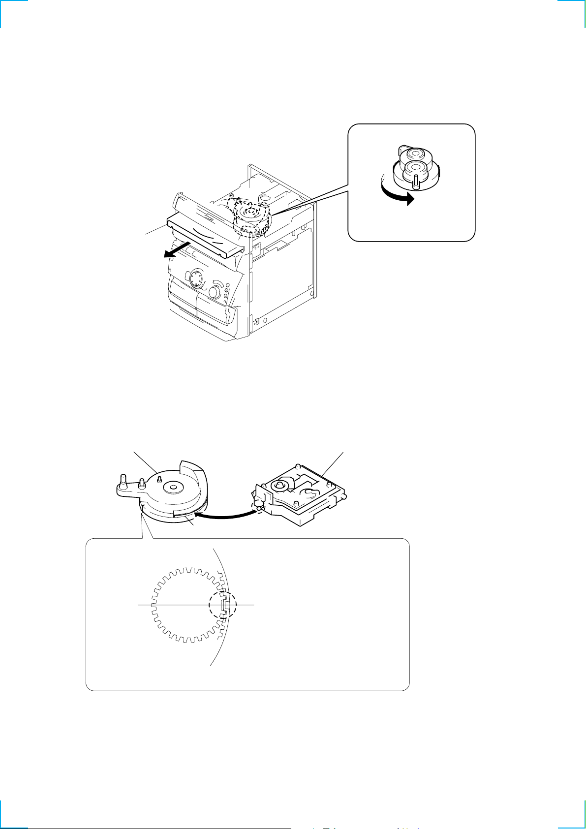
HOW TO OPEN THE DISC TRAY WHEN POWER SWITCH
TURNS OFF
1
Remove the Case.
3
Pull-out the disc tray.
2
Turn the cam to the direction
of arrow.
Note for Installation (ROTARY ENCODER)
BU cam
Groove
Note:When attaching the Base unit, Insert the
section A into the groove of BU cam.
Section A
Note:When attaching the BU cam,
engage the Rotary encoder
switch as shown in the figure.
CD-TEXT
This unit is provided with a simple CD-TEXT display function.
The CD-TEXT contents of 20 tracks are displayed on the fluorescent display tube.
Since the function is simple, some special characters may not be displayed, or may be displayed as other characters.
4
SELF-DIAGNOSIS
3
This unit is equipped with a self-diagnosis function.
The function is used for diagnosing the conditions of the circuits of
the VIDEO board.
The circuits can be determined if normal or abnormal by the lighting of D502 of the VIDEO board.
Lighting of D502
When lit : Operates normally
Blinks repeatedly : The circuit may be faulty.
[VIDEO BOARD] (SIDE B)
NOTES ON HANDLING THE OPTICAL PICK-UP BLOCK
OR BASE UNIT
The laser diode in the optical pick-up block may suffer electrostatic
break-down because of the potential difference generated by the
charged electrostatic load, etc. on clothing and the human body.
During repair, pay attention to electrostatic break-down and also
use the procedure in the printed matter which is included in the
repair parts.
The flexible board is easily damaged and should be handled with
care.
NOTES ON LASER DIODE EMISSION CHECK
The laser beam on this model is concentrated so as to be focused on
the disc reflective surface by the objective lens in the optical pickup block. Therefore, when checking the laser diode emission, observe from more than 30 cm away from the objective lens.
31
50
IC505
51
CN502
130
80
D502
CN501
100
81
SL501
SL502
SL50
5

MC Cold Reset
• The cold reset clears all data including preset data stored in the RAM to initial conditions. Execute this mode when returning the set to the
customer.
Procedure:
1. Press three buttons p , ENTER/NEXT , and 1/u simultaneously.
2. “COLD RESET” is displayed on the fluorescent display tube and reset is executed.
CD Delivery Mode
• This mode moves the optical pick-up to the position durable to vibration. Use this mode when returning the set to the customer after repair.
Procedure:
1. Press 1/u button to turn the set ON.
2. Press CD LOOP button and 1/u button simultaneously.
3. A message “LOCK” is displayed on the fluorescent indicator tube, and the CD delivery mode is set.
MC Hot Reset
• This mode resets the set with the preset data kept stored in the memory. The hot reset mode functions same as if the power cord is plugged
in and out.
Procedure:
1. Press three buttons p , ENTER/NEXT , and DISC 1 simultaneously.
2. The fluorescent indicator tube becomes blank instantaneously, and the set is reset.
Sled Servo Mode
• This mode can run the CD sled motor freely. Use this mode, for instance, when cleaning the optical pick-up.
Procedure:
1. Press 1/u button to turn the set ON.
2. Press three buttons p , ENTER/NEXT , and § simultaneously.
3. The Sled Servo mode is selected, if “CD” is blanking on the fluorescent indicator tube.
4. With the CD in stop status, When the ) + button is pressed, the optical pick-up moves outside. When – 0 button is pressed, it
moves inside.
5. To exit from this mode, perform as follows:
1) Move the optical pick-up to the most inside track.
2) Execute MC cold reset. (Press the three buttons p , ENTER/NEXT , and 1/u button simultaneously.)
Note:
• Always move the optical pick-up to most inside track when exiting from this mode. Otherwise, a disc will not be unloaded.
• Do not run the sled motor excessively, otherwise the gear can be chipped.
Change-over of AM Tuner Step between 9kHz and 10kHz
• A step of AM channels can be changed over between 9kHz and 10kHz.
Procedure:
1. Press 1/u button to turn the set ON.
2. Select the function “TUNER”, and press TUNER/BAND button to select the BAND “AM”.
3. Press 1/u button to turn the set OFF.
4. Press ENTER/NEXT and 1/u buttons simultaneously, and the display of fluorescent indicator tube changes to “AM 9k STEP” or “AM
10k STEP”, and thus the channel step is changed over.
LED and Fluorescent Indicator Tube All Lit, Key Check Mode
Procedure:
1. Press three buttons p , ENTER/NEXT , and DISC 2 simultaneously.
2. LEDs and fluorescent indicator tube are all turned on.
Press DISC 2 button, and the key check mode is activated.
3. In the key check mode, the fluorescent indicator tube displays “K 0 V0 J0”. Each time a button is pressed, “K”value increases. However ,
once a button is pressed, it is no longer taken into account.
“J” V alue increases like 1, 2, 3 ... if rotating 0 AMS ) knob in “+” direction, or it decreases like 0, 9, 8 ... if rotating in “-” direction.
“V” Value increases like 1, 2, 3 ... if rotating VOLUME knob in “+” direction, or it decreases like 0, 9, 8 ... if rotating in “-” direction.
4. To exit from this mode, press three buttons in the same manner as step 1, or disconnect the power cord.
6

AMS Test Mode
H
g
g
H
H
g
3
• This mode is used for checking the AMS operations of the tape deck.
JIG
7-819-039-12 Alignment tape, AMS-110A
Procedure:
1. Press the 1/u button to turn the unit ON.
2. Set the tape (AMS-110A).
3. Press the three buttons p , ENTER/NEXT , and DISC 3 button simultaneously.
4. “TEST MODE” is displayed on the fluorescent display tube.
5. Press the FUNCTION button and switch the function to the deck with the tape (AMS-110A).
6. Press the CD SYNC button. “AMS CHECK” is displayed on the fluorescent display tube and the tape is rewound.
7. AMS starts in the normal direction. If the AMS count is 2 at shut down, proceed to step 8.
“NG” is displayed at other times, and the deck stops.
8. AMS starts in the opposite direction. If the AMS count is 2 at shut down again, “OK” is displayed.
“NG” is displayed at other times.
Note: The p button of CD section will become effective and the aging of CD section will stop sometime, if the buttons described in step 3
are not pressed simultaneously. In that case, press ^ button and operate the CD section.
SELF-DIAGNOSIS
This model has the self-diagnosis function for the VIDEO and AUDIO decoder sections.
Immediately after the power on, the self-diagnosis function searches each operation of IC’s around the mechanism control microcomputer
(IC701).
The results can be checked by D502 of the VIDEO board.
Oscilloscope (Waveform) Symptom
No error
Li
ht
L
MPEG decoder (IC506)
L
2 time blinkin
error
MPEG decoder (IC506)
or
3 time blinkin
L
DRAM (IC507) error
[VIDEO BOARD] (SIDE B)
(GND)
CT503
VIDEO
Frequency
Adjustment
Check point
(27 MHz)
31
50
51
IC505
80
130
CN501
100
81
SL501
SL502
CN502
D502
SL50
7

Aging Mode
This mode can be used for operation check of tape deck section.
• If an error occurred:
The aging operation stops and display then status.
• If no error occurs:
The aging operation continues repeatedly.
• The sequence during the aging mode is following as below.
• If an error occurred, stop display that step.
Aging mode sequence:
Procedure:
1. Load the tapes into the decks A and B respectively.
2. Press the FUNCTION button to select the function “CD”.
3. Press the PLAY MODE button to set the “ALL DISCS” mode,
and press the REPEAT button to “REPEAT” off.
4. Press three buttons of p , ENTER/NEXT , and DISC SKIP/
EX-CHANGE simultaneously.
5. The aging mode is activated, if the indicator of disc tray number
on the fluorescent indicator tube is blinking.
6. To exit from the aging mode, press the 1/u button to turn the
power OFF and operate the cold reset. (Refer to the “MC Cold
Reset”)
Rewind the tape A and B
“TAPE A AG-1”
Shut off
FWD piay the tape A
“TAPE A AG-2”
2 mimutes
Fast forward the tape A
“TAPE A AG-3”
Shut off or 20 seconds
REV play the tape A
“TAPE A AG-4”
2 minutes
Rewind the tape A
“TAPE A AG-5”
Shut off
FWD play the tape B
“TAPE B AG-2”
2 minutes
Fast forward the tape B
“TAPE B AG-3”
Shut off or 20 seconds
REV play the tape B
“TAPE B AG-4”
2 minutes
Rewind the tape B
“TAPE B AG-5”
Shut off
Note: “T APE * AG_*” is display of each step.
8
VIDEO CD COLOR-BARS MODE
On this mode, the data of the color-bars signal as a picture signal and the 1kHz sine wave signal as a sound signal are output by the
mechanism control microcomputer (IC505) for video CD signal check. When measurement of the voltage and waveform on the VIDEO
board, perform it in this mode.
For reference, the color-bars signal can be observed at J502 (VIDEO OUT) and the sound signal can be observed at J101 (VIDEO/MD
(AUDIO) OUT) using an oscilloscope.
1. Connect the lead wire to both ends of the land of SL503 of the VIDEO board.
2. Turn the power on. Press FUNCTION button to select CD.
3. After 2 or 3 seconds later, connect the lead wire.
4. After measuring, remove the lead wire connected.
[VIDEO BOARD] (SIDE B)
3150
51
30
CN502
SL503
SL502
80
81
SL501
IC505
1
100
CN501
9

SECTION 2
GENERAL
Front Panel
44 4345
321
64
63
62
61
60
56575859
55
51525354
47484950
46
42
39
4041
3738
36
4567
15 14 13
20
22 21
8
9
10
11
12
1819 17 16
23
24
3435
LOCATION OF PARTS AND CONTROLS
1 1/u button and indicator
2 DEMO (ST ANDBY) button
3 DISC 1 button and indicator
4 DISC 2 button and indicator
5 DISC 3 button and indicator
6 DISC SKIP/EX–CHANGE button
7 § (Eject) button
8 SYNC BASS H indicator
9 SVIDEO/VCD indicator
10 PBC indicator
11 PBC OFF indicator
12 SYNC BASS L indicator
13 TUNER/BAND button
14 ^ (CD) button and indicator
15 p button
16 SYNC BASS button
17 SYNC EQ button
18 KARAOKE PON/MPX button
19 CD NON-STOP button and indicator
20 REC P AUSE/START button and
indicator
21 DSP button and indicator
22 DBFB button
23 HI-DUB button
24 CD SYNC button
25 PHONES jack
26 VOLUME knob
27 ENTER/NEXT button and indicator
28 ) + button and indicator
29 PRO LOGIC button and indicator
30 JOG/0x) dial and indicator
31 GROOVE button and indicator
32 0 – button and indicator
33 DVD 5.1 CH button
34 CD FLASH button
35 CD LOOP button
36 MIC 2 jack
37 TIMER SELECT button and indicator
38 CLOCK/TIME SET button
39 MIC 1 jack
40 SPECTRUM ANALYZER button
41 DISPLAY button
42 MIC LEVEL knob
43 REPEA T/STEREO/MONO button
10
25
26
27
28
29
30
33 32 31
44 PLAY MODE/DOLBY NR button
45 EDIT DIRECTION TUNER MEMORY
button
46 ECHO LEVEL knob
47 P FILE MEMORY button
48 GEQ CONTROL button
49 FILE SELECT button
50 EFFECT button
51 NEXT button
52 PREV button
53 RETURN button
54 SELECT button
55 ( (TAPE B) button and indicator
56 9 (TAPE B) button and indicator
57 ( (TAPE A) button and indicator
58 9 (TAPE A) button and indicator
59 FUNCTION button
60 SYNC EQ indicator
61 Remote sensor
62 EFFECT indicator
63 Display Window
64 Disc tray

This section is extracted from
instruction manual.
11

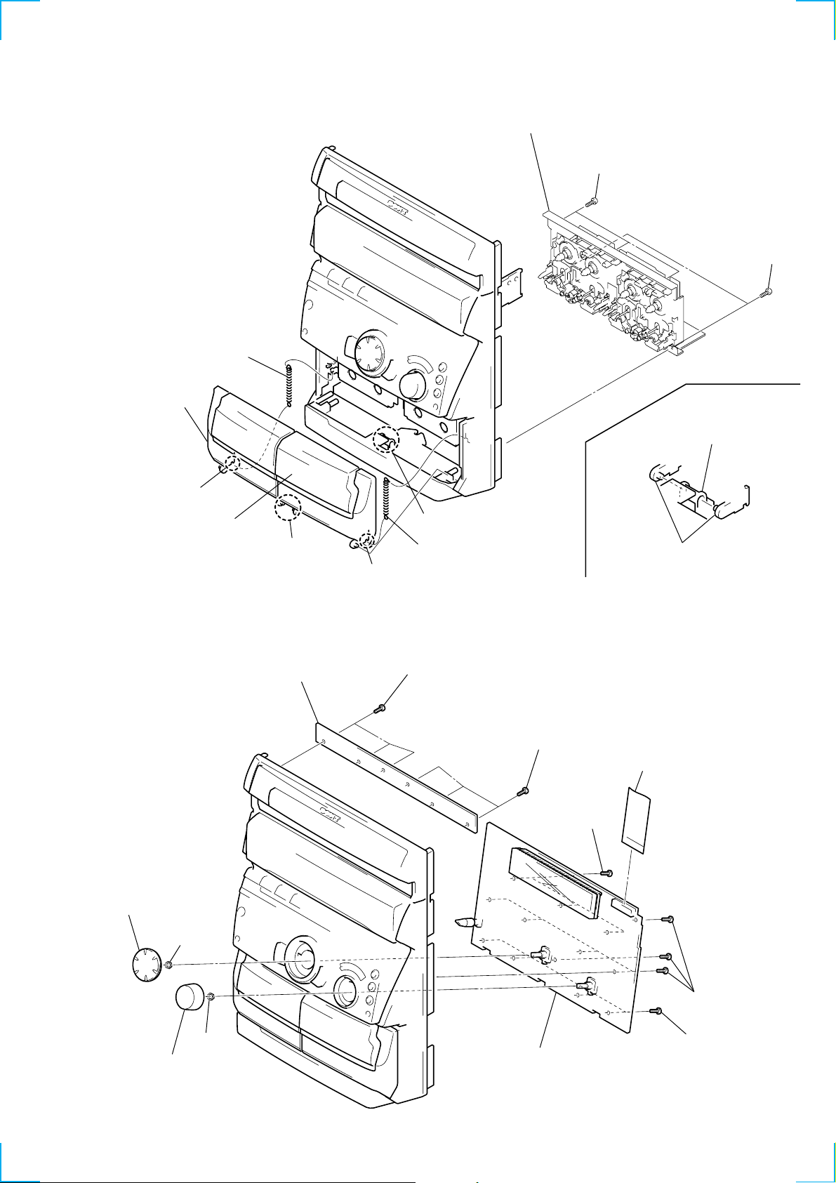
SECTION 3
)
DISASSEMBLY
Note: Follow the disassembly procedure in the numerical order given.
3-1. LOADING PANEL
Claws
3
Loading panel
assembly
2
Pull-out the disc tray.
1
Turn the cam to the direction
of arrow.
3-2. FRONT PANEL
2
Screw (BVTT 3x6)
6
Screw (BVTP 3x10)
0
Front panel
4
8
(CN131)
Lead wire
Screw (BVTT 3x8)
9
(CN132)
Flat type wire
5
(BVTP3x10)
!¢
Screw (BVTP 3x8)
!™
Flat type wire
(CN502)
Flat type wire
Screw
7
Flat type wire
(CN141)
!∞
Video board
!¡
(CN501)
Lead wire
1
Screw (BVTT 3x6)
Flat type wire
!£
Two screws (BVTP 3x8)
12
3
Screw (BVTT 3x8
3-3. CASSETTE LID AND TAPE MECHANISM
6
T ension spring
4
Cassette holder (L)
assembly
2
Release
9
T ape mechanism
8
Three screws
(BVTP2.6x8)
7
T wo screws
(BVTP2.6x8)
Note for installation
Portion
B
3
Cassette holder (R)
assembly
Portion
A
3-4. CD SW BOARD AND PANEL BOARD
3
CD SW board
4
Knob (Jog)
1
Release
Portion
B
5
T ension spring
1
Three screws
(BVTP2.6x8)
2
Three screws
(BVTP2.6x8)
9
Three screws
(BVTP2.6x8)
Portion
8
Flat type wire
(CN601)
A
6
Nut
5
Knob (Vol)
7
Nut
!™
Panel board
0
Six screws
(BVTP2.6x8)
!¡
Four screws
(BVTP2.6x8)
13

3-5. DISC TRAY
(Perform after removing the front panel.) Note:When installing the Disc tray, pull around the flat type wire to
3
Flat type wire (8 core)
4
Two claws
2
Pull-out the disc tray.
5
Remove the disc tray.
pass through the claw
Claw
A
A
and claw B, as shown in the figure.
Claw
B
1
Turn the cam the
direction of arrow.
14

SECTION 4
MECHANICAL ADJUSTMENTS
SECTION 5
ELECTRICAL ADJUSTMENTS
Precaution
1. Clean the following parts with a denatured alcohol-moistened
swab:
record/playback heads pinch rollers
erase head rubber belts
capstan idlers
2. Demagnetize the record/playback head with a head demagnetizer.
3. Do not use a magnetized screwdriver for the adjustments.
4. After the adjustments, apply suitable locking compound to the
parts adjusted.
5. The adjustments should be performed with the rated power supply voltage unless otherwise noted.
Torque Measurement
Mode
FWD
FWD
back tension
REV
REV
back tension
FF/REW
FWD tension
REV tension
Torque meter
CQ-102C
CQ-102C
CQ-102RC
CQ-102RC
CQ-201B
CQ-403A
CQ-403R
Meter reading
31 to 71 g • cm
(0.43 – 0.98 oz • inch)
2 to 6 g • cm
(0.02 – 0.08 oz • inch)
31 to 71 g • cm
(0.43 – 0.98 oz • inch)
2 to 6 g • cm
(0.02 – 0.08 oz • inch)
71 to 143 g • cm
(0.98 – 1.99 oz • inch)
100 g or more
(3.53 oz or more)
100 g or more
(3.53 oz or more)
DECK SECTION 0 dB=0.775V
1. Demagnetize the record/playback head with a head damagnetizer.
2. Do not use a magnetized screwdriver for the adjustments.
3. After the adjustments, apply suitable locking compound to the
parts adjusted.
4. The adjustments should be performed with the rated power supply voltage unless otherwise noted.
5. The adjustments should be performed in the order given in this
service manual. (As a general rule, playback circuit adjustment
should be completed before performing recording circuit adjustment.)
6. The adjustments should be performed for both L-CH and R-CH.
7. Switches and controls should be set as follows unless otherwise
specified.
Signal
P-4-A100
WS-48B
P-4-L300
10 kHz, –10 dB
3 kHz, 0 dB
315 Hz, 0 dB
Record/Playback Head Azimuth Adjustment
(Deck A, Deck B)
Note: Perform this adjustments for both decks.
Procedure:
1. Mode : Playback
Used forT ape
Azimuth Adjustment
Tape Speed Adjustment
Level Adjustment
test tape
P-4-A100
(10kHz, –10dB)
set
MD OUT
(J101)
level meter
+
–
2. Turn the adjustment screw and check output peaks. If the peaks
do not match for L-CH and R-CH, turn the adjustment screw so
that outputs match within 1 dB of peak.
L-CH
peak
screw
position
R-CH
peak
output
level
within
1 dB
L-CH
peak
R-CH
peak
within 1dB
screw
position
15

3. Mode: Playback Tape Speed Adjustment (Deck B)
)
test tape
P-4-A100
(10kHz, –10dB)
oscilloscope
MD OUT
(J101)
set
Note: Set the test mode using the following method and begin tape
speed adjustment.
In the test mode, the speed will switch to double speed or
normal speed each time the HI DUB button is pressed.
Procedure:
With the power turned ON, press the p button, ENTER/NEXT
button, and DISC 3 button simultaneously.
(The “CD TYPE INDICA T OR” on the fluorescent display tube will
blink while in the test mode.)
T o exit the test mode, press the 1/u button.
Waveform of oscilloscope
in phase 45
good
°
135
90
°
°
wrong
180
°
4. After the adjustments, apply suitable locking compound to the
parts adjusted.
Adjustment Location: Playback Head (Deck A)
Record/Playback/Erase Head (Deck B)
Reverse Foward
1. Insert the WS-48B into deck B.
2. Press the ^ button of deck B.
3. Press the HI DUB button and play the tape at double speed.
4. Adjust RV1001 of the LEAF SW board so that the reading of
the frequency counter becomes 6000 ± 180 Hz.
5. Press the HI DUB button and play the tape at normal speed.
6. Adjust RV1002 of the LEAF SW board so that the reading of
the frequency counter becomes 3000 ± 90 Hz.
Adjustment Location: LEAF SW board
Sample Value of Wow and flutter
W.RMS (JIS) less than 0.3%
(test tape: WS-48B)
Playback Level Adjustment (Deck A, Deck B)
Procedure:
Mode: Playback
test tape
P-4-L300
(315Hz, 0dB)
set
MD OUT
(J101)
level meter
16
Deck A is RV311 (L-CH) and RV411 (R-CH), deck B is RV301
(L-CH) and RV401 (R-CH)
so that adjustment within the following adjustment level.
Adjustment level:
J101 playback level: 301.5 to 338.3 mV (–8.2 to –7.2 dB)
level difference between the channels: within ± 0.5 dB
Adjustment Location: AUDIO board
Adjustment Location
[LEAF SW BOARD]
RV1001(High Speed)
RV1002(Normal Speed
RV1002 RV1001

Record Bias Adjustment (Deck B)
AF OSC
VIDEO (AUDIO) IN (J101)
315Hz 50 mV (–23.8 dB)
blank tape
CS-123
set
attenuator
600
Ω
IC301
Record Level (L CH)
RV301
CN303
RV351
Record Level (R CH)
56
43
42
29
28
15
14
1
Record Level Adjustment (Deck B)
Procedure:
INTRODUCTION
When set to the test mode performed in Tape Speed Adjustment, when the tape is rewound after recording, the “REC memory
mode” which rewinds only the recorded portion and playback is
set.
This “REC memory mode” is convenient for performing this adjustment. During recording, the input signal FUNCTION will automatically switch to VIDEO.
(After recording, press the – 0 button without stopping will
return to the position where recording was started.)
1. Press FUNCTION button to select VIDEO. (This step is not
necessary if the above test mode has already been set.)
2. Insert a tape into deck B, press the r REC button, and then
press the ^ button to start recording.
3. Mode: Record
VIDEO (AUDIO) IN (J101)
1) 315 Hz
2) 10 kHz
AF OSC
attenuator
600
Ω
} 50 mV (–23.8 dB)
blank tape
CS-123
set
Procedure:
INTRODUCTION
When set to the test mode performed in Tape Speed Adjustment, when the tape is rewound after recording, the “REC memory
mode” which rewinds only the recorded portion and playback is
set.
This “REC memory mode” is convenient for performing this
adjustment. During recording, the input signal FUNCTION will automatically switch to VIDEO.
(After recording, press the – 0 button without stopping will
return to the position where recording was started.)
1. Press FUNCTION button to select VIDEO 1. (This step is not
necessary if the above test mode has already been set.)
2. Insert a tape into deck B, press the r REC button, and then
press the ^ button to start recording.
3. Mode: Record
4. Mode: Playback
5. Confirm playback the signal recorded in step 2 become adjust-
Adjustment level: The playback output of 10 kHz level difference
Adjustment Location: AUDIO board
Adjustment Location:
[AUDIO BOARD] (Conductor Side)
recorded
position
set
MD OUT
(J101)
level meter
ment level as follows.
If these levels do not adjustment level, adjust the R V341 (L-CH)
and R V441 (R-CH) on the AUDIO board to repeat steps 3 and 4.
against 315 Hz reference should be ± 1.0 dB.
RV341(Lch),RV441(Rch)
Record Bias
RV311(Lch),RV411(Rch)
Playback Level (Deck A)
4. Mode: Playback
recorded
position
set
MD OUT
(J101)
level meter
5. Confirm playback the signal recorded in step 2 become adjustment level as follows.
If these levels do not adjustment level, adjust the R V301 (L-CH)
and R V351 (R-CH) on the MAIN board to repeat steps 3 and 4.
Adjustment level:
J301 playback level: 47.2 to 53.0 mV (–24.3 to –23.3 dB)
Adjustment Location: MAIN board
[MAIN BOARD] (Conductor Side)
RV301 RV401
RV441 RV341
RV301(Lch),RV401(Rch)
Playback Level (Deck B)
RV311
RV411
17
CD SECTION
Note:
1. CD Block is basically constructed to operate without adjustment.
Therefore, check each item in order given.
2. Use YEDS-18 disc (3-702-101-01) unless otherwise indicated.
3. Use an oscilloscope with more than 10MΩ impedance.
4. Clean the object lens by an applicator with neutral detergent when
the signal level is low than specified value with the following
checks.
Note: Clear RF signal waveform means that the shape “◊” can be
clearly distinguished at the center of the waveform.
RF signal waveform
VOLT/DIV : 200mV
TIME/DIV : 500ns
level : 1.45 ± 0.3 Vp-p
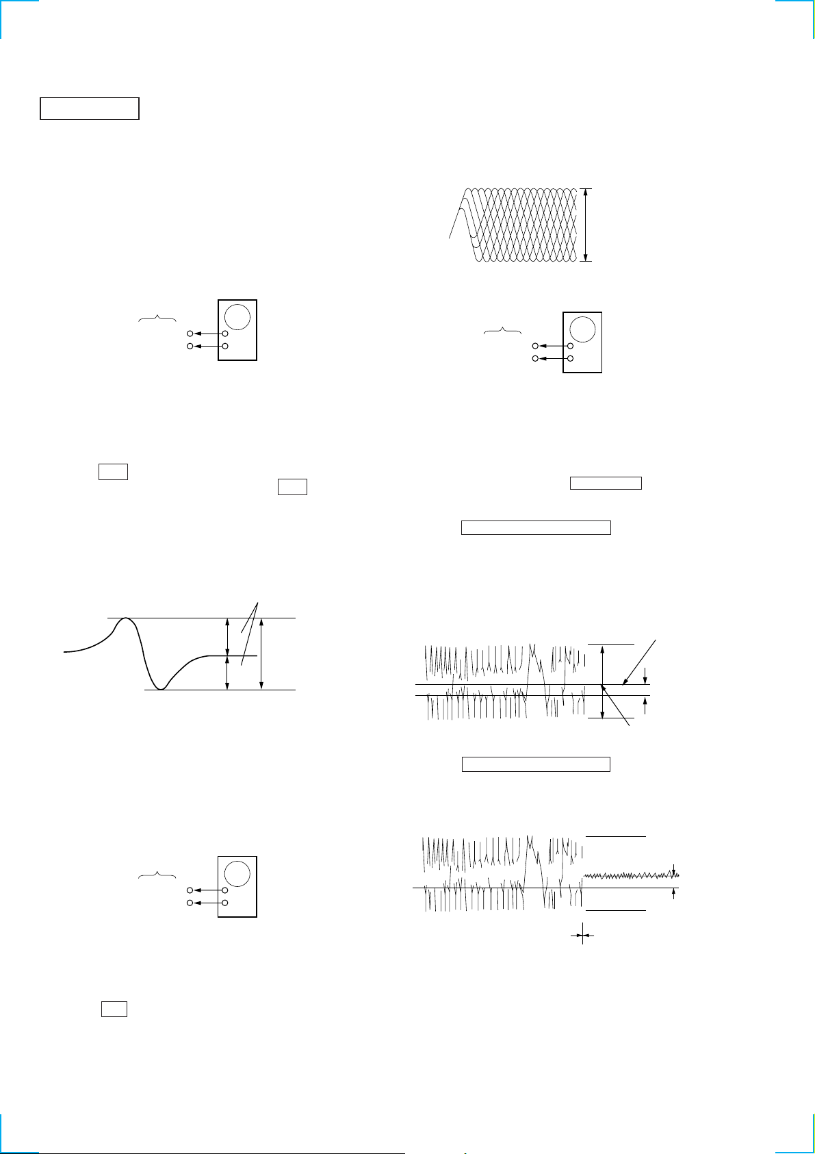
S Curve Check
oscilloscope
BD board
TP (FE)
TP (VC)
+
–
Adjustment Location: BD board
Procedure :
1. Connect the oscilloscope to test points TP (FE) and TP (VC).
2. Connect TP (FE1) and TP (VC), and TP (AGCCON) and GND
of the BD board with lead wires.
3. Press the 1/u button to turn the set ON.
4. With the disc (YEDS-18) loaded, press the ^ button and
perform focus search. (Focus search will be performed in the
same way even while the disc table is pushed in and out.)
5. Check the symmetry and peak to peak level of the oscilloscope
waveform (S curve) at this time.
S-curve waveform
symmetry
A
Within 4.0
B
±
1.0 Vp-p
6. After check, remove the lead wire connected in step 2.
Note: • Try to measure several times to make sure than the ratio of
A : B or B : A is more than 10 : 7.
• Take sweep time as long as possible and light up the brightness to obtain best waveform.
Adjustment Location: BD board
E-F Balance (Traverse) Check
oscilloscope
BD board
TP (TE)
TP (VC)
+
–
Adjustment Location: BD board
Procedure :
1. Connect oscilloscpe to test point TP (TE) and TP (VC) on BD
board.
2. Short-circuit SL502 of the video board to GND.
3. Turned Power switch on. Press FUNCTION button to select
CD.
4. Put disc (YEDS-18) in to play the number five track.
5. Press the PLAY MODE/DOLBY NR button. (The tracking
servo and the sledding servo are turned OFF .)
6. Check the level B of the oscilliscope's waveform and the A (DC
voltage) of the center of the Traverse waveform.
Confirm the following :
A/B x 100 = less than ± 22%
Traverse waveform
0V
Center of the waveform
B
A (DC voltage)
level : 1.3 ± 0.6 Vp-p
7. Press the PLAY MODE/DOLBY NR button. (The tracking
servo and sledding servo are turned ON.) Confirm the C (DC
voltage) is almost equal to the A (DC voltage) is step 7.
RF Level Check
oscilloscope
BD board
TP (RF)
TP (VC)
+
–
Procedure :
1. Connect oscilloscope to test point TP (RF) and TP (VC) on BD
board.
2. Connect TP (AGCCON) and GND of the BD board with lead
wires.
3. Press the 1/u button to turn the set ON.
4. Put disc (YEDS-18) in and playback 5track.
5. Confirm that oscilloscope waveform is clear and check RF signal level is correct or not.
6. After check, remove the lead wire connected in step 2.
18
Traverse waveform
0V
Tracking servo
Sled servo
OFF
Tracking servo
Sled servo
ON
8. Desolder the short-land (SL502) short-circuited at step 2.
Adjustment Location: BD board
C (DC
voltage)

Adjustment Location :
3
[BD BOARD] (SIDE B)
TP (RF)
TP (VC)
TP
(AGCCON)
IC102
TP (FE)
TP (FE)
VIDEO SECTION
IC103
TP (TE)
IC101
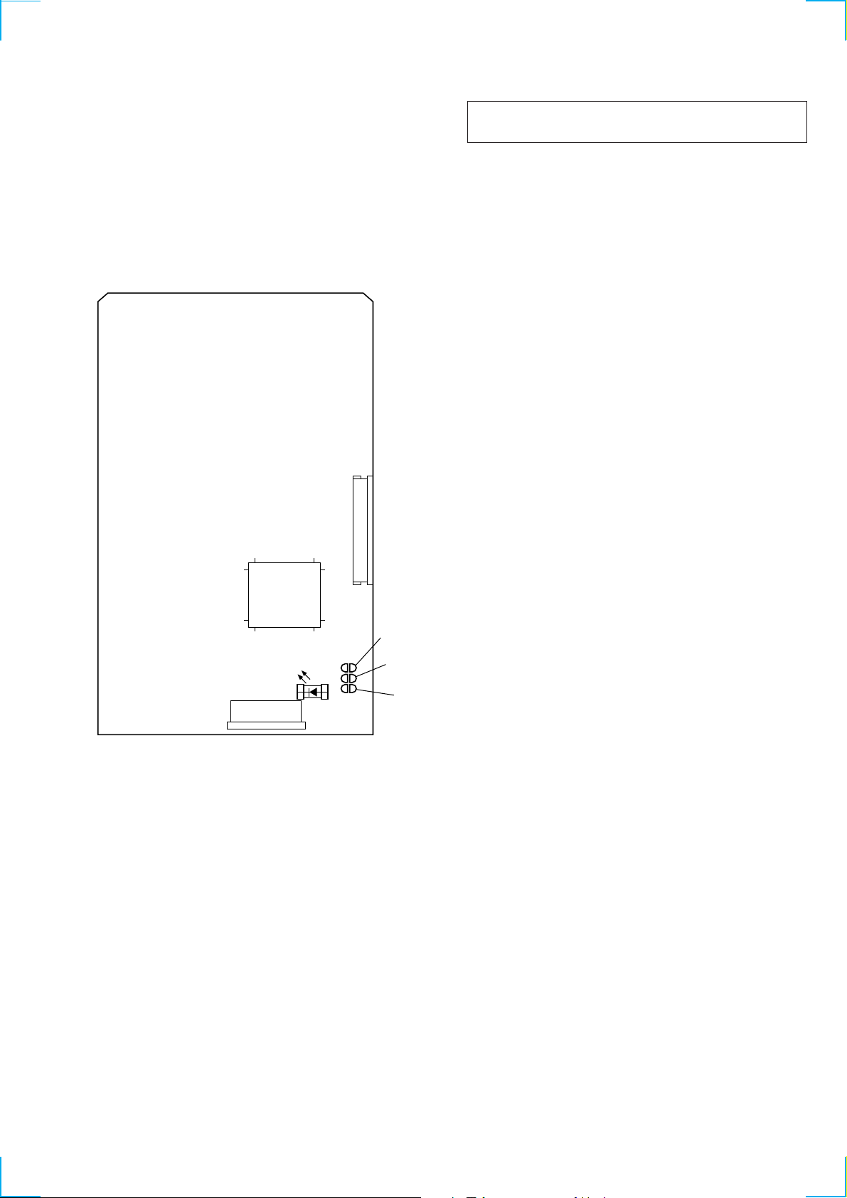
Frequency adjustment
1. Connect the frequency counter to check point (27MHz) of the
VIDEO board.
2. Adjust CT503 of the VIDEO board so that the frequency counter
read 27MHz ± 80Hz at STOP condition.
Adjustment Location :
[VIDEO BOARD] (SIDE B)
(GND)
CT503
VIDEO
Frequency
Adjustment
31
Check point
(27 MHz)
50
51
130
IC505
80
CN501
100
81
SL501
SL502
VIDEO board
(27 MHz)
frequency counter
+
–
CN502
D502
SL50
19
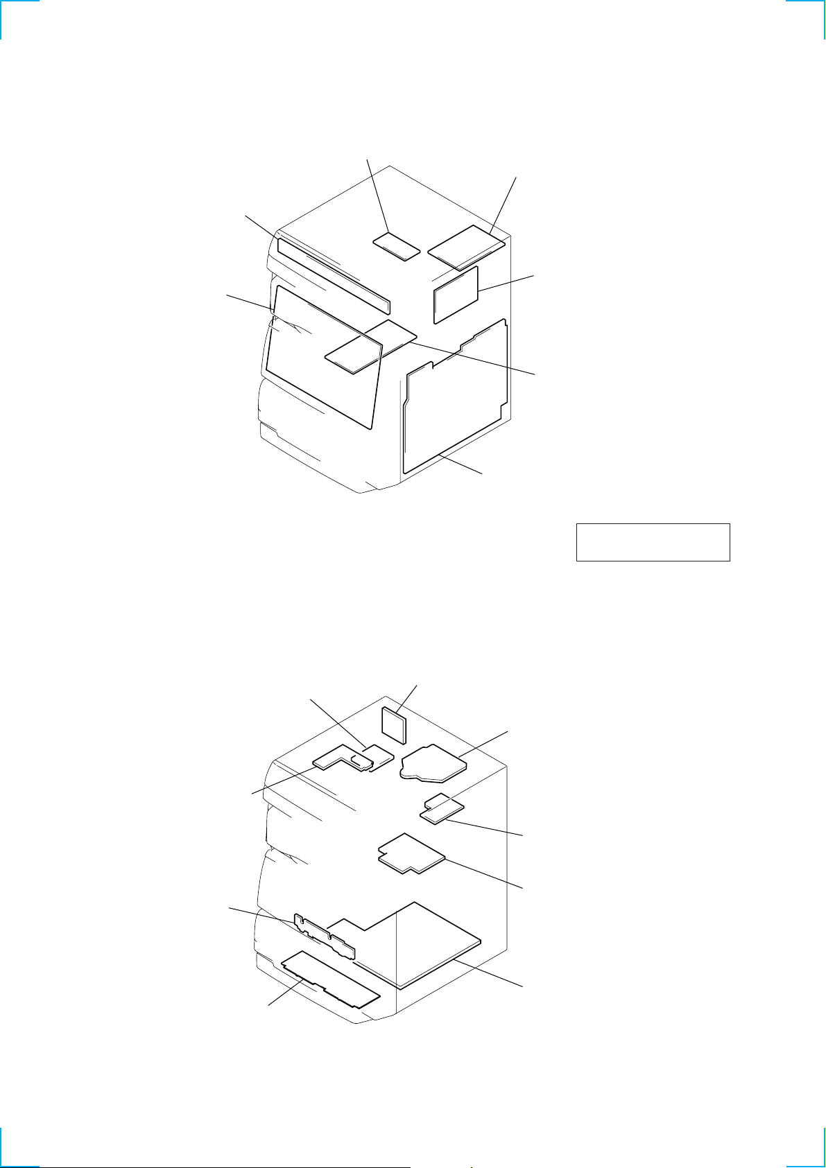
6-1. CIRCUIT BOARDS LOCATION
CD SW board
PANEL board
SECTION 6
DIAGRAMS
5V power board
VIDEO board
TUNER unit
TRANS board
SENSOR board
MAIN board
TUNER unit is supplied as
the assembled block.
MOTOR (TURN) board
CONNECTOR board
BD board
MOTOR (SLIDE) board
20
3CH AMP board
LEAF SW board
FRONT AMP board
AUDIO board
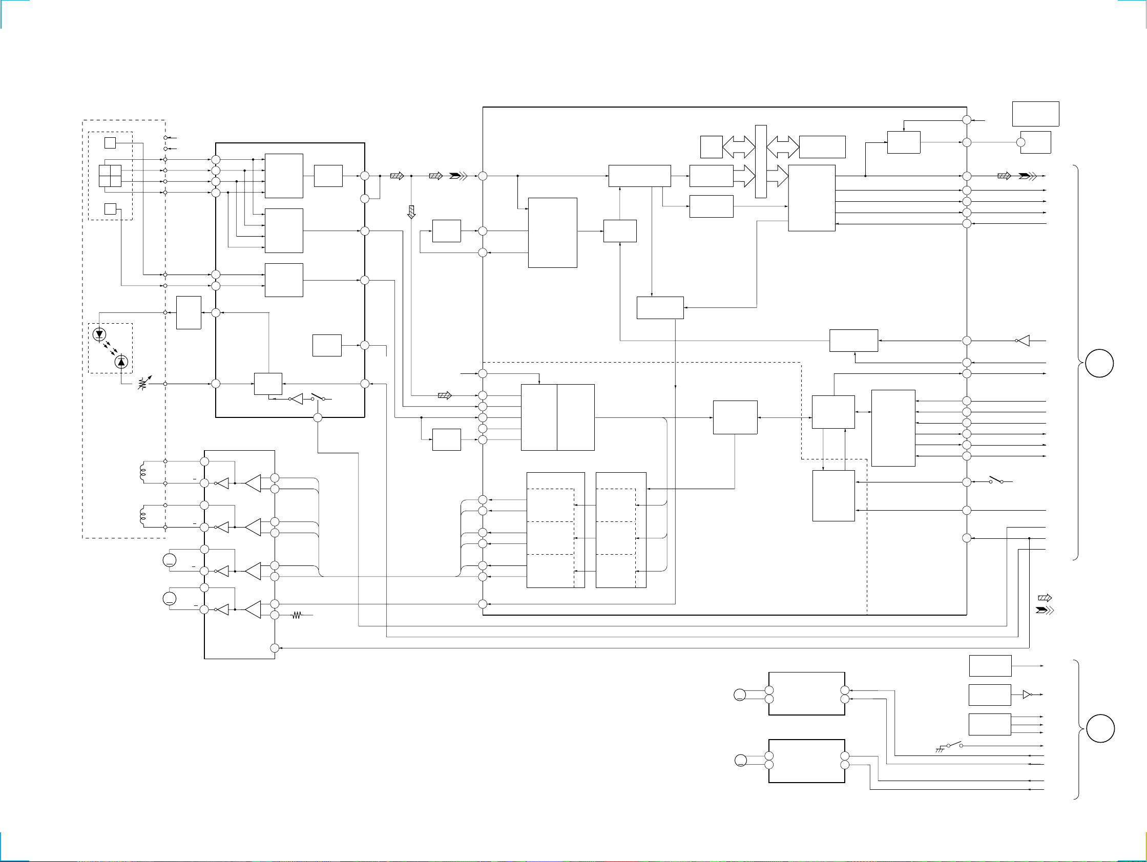
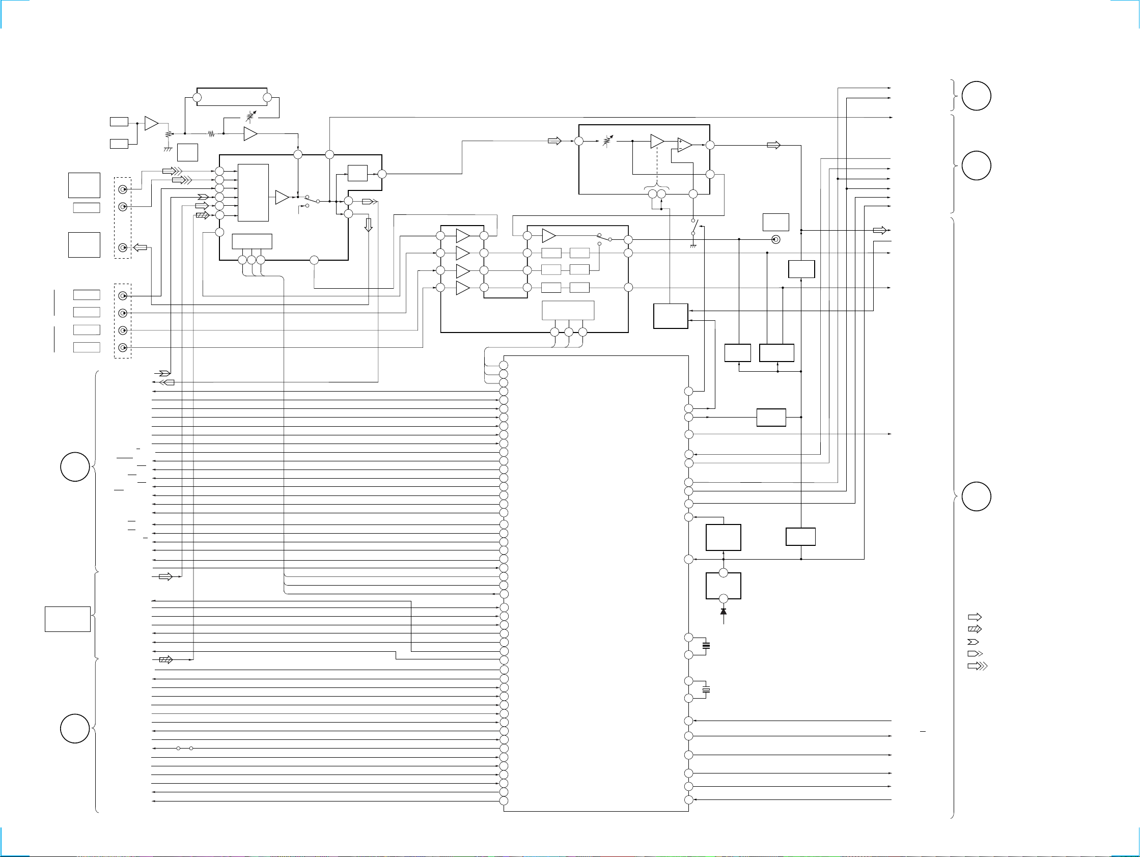
6-2. BLOCK DIAGRAMS
– CD SECTION –
OPTICAL PICK-UP BLOCK
(KSS-213D/Q-NP)
DETECTOR
E
A
A
C
D
B
F
C
D
B
VCC
VC
HCD-VX880AV
IC421
CD DIGITAL
IC101
IC103
RF AMP
A
5
C
7
D
8
B
6
RF
SUMMING
AMP
FOCUS
ERROR
AMP
RF EQ
AMP
RFD
RFI
FE
16
17
14
INTEGRATOR
DIGITAL SERVO
DIGITAL SIGNAL PROCESSOR
RF AC
50
ASYI
49
ASYO
48
ASYMMETRY
CORRECTION
DEMODULATOR
DIGITAL
PLL
EFM
32K
RAM
REGISTER
SUB CODE
PROCESSOR
DATA BUS
ERROR
CORRECTOR
D/A
INTERFACE
DIGITAL
OUT
MD2
D OUT
PCM-D
BCLK
LRCK
C2PO
MUTE
63
D+5V
64
66
67
65
14
3
OPTICAL
1
OUT
DOUT
ADATA
BCLK
LRCK
C2PO
MUTE
LD
PD
TRACKING
COIL
FOCUS
COIL
LASER
DIODE
LD
POWER
M102
SLED
MOTOR
M101
SPINDLE
MOTOR
E
F
LD
DRIVE
Q101
T+
T
F+
F
SD+
M
SD
SP+
M
SP
E
11
F
10
LD
3
PD
4
FOCUS/TRACKING COIL DRIVE
SPINDLE/SLED MOTOR DRIVE
12
11
14
13
17
18
15
16
IC102
APC LD
AMP
TRACKING
ERROR
AMP
5
6
2
3
24
23
25
27
TFDR
TRDR
FFDR
FRDR
SFDR
SRDR
BUFFER
21
VC
VC
REF
LD ON
TE
13
DIGITAL
CLV
IC104
4
A+5V
(XTAL 33.8MHz)
MCK
2
CTRL1
SENS
DATA
XLT
CLK
SCOR
SUBQ
SQCK
SCLK
LPH
XRST
LD ON
• SIGNAL PATH
: CD
: VIDEO
A
VIDEO
SECTION
(Page 22)
CLOCK
12
VC
38
INTEGRATOR
VC
RFDC
43
FE
39
TE
41
CE
42
VC
SE
40
TFDR
31
TRDR
32
FFDR
33
FRDR
34
SFDR
29
SRDR
30
MDP
25
OP AMP
ANALOG SW
PWM
GENERATOR
TRACKING
PWM
GENERATOR
FOCUS
PWM
GENERATOR
SLED
PWM
GENERATOR
CONVERTER
22
A/D
CONTROL SIGNAL
BLOCK
SERVO
BLOCK
SERVO DSP
TRACKING
SERVO
FOCUS
SERVO
SLED
SERVO
DETECTOR
MIRR
DFCT
FOK
GENERATOR
SERVO
AUTO
SEQUENCER
SERVO
INTERFACE
CPU
INTERFACE
XTAI
XTSL
SENS
DATA
XLAT
CLOK
SCOR
SQSO
SQCK
S STOP
SCLK
XRST
71
69
7
4
5
6
15
76
77
26
S101
LIMIT SW
8
82
MUTE
M701
TURN
M
MOTOR
M801
SLIDE
MOTOR
09
7
2
4
M
7
MOTOR DRIVER
OUT1
OUT2
MOTOR DRIVER
OUT2
OUT1
TURN
IC701
SLIDE
IC801
RIN
IN1
IN2
FIN
TABLE
SENSOR
IC702
3
6
S801
OPEN/CLOSE
2
10
DET
DISC
SENSOR
IC703
ROTARY
ENCODER
S811
Q701
T. SENS
DISC SENS
ENC 1
ENC 2
ENC 3
OPEN
TBL.L
TBL.R
LOAD IN
LOAD OUT
C
MAIN
SECTION
(Page 24)
XRST
20
21 21

HCD-VX880AV
– VIDEO SECTION –
MCLK 33.8MHz
DIGITAL FILTER,
D/A CONVERTER
IC509
A
CD
SECTION
(Page 21)
A DATA
BCK
LRCK
C2PO
LEVEL
SHIFT
IC503
MPEG VIDEO/AUDIO DECODER,
VIDEO SIGNAL PROCESSOR
IC506
CD-DATA
180
CD-BCK
184
CD-LRCK
182
CD-C2PO
185
100,98,114,116,118,120,121,122,124
ADDRESS BUS
DATA BUS
CD-ROM
INTERFACE
CIRCUIT
MA0 – MA10
104,110,112,111,108,105,102,99,96,
A0 – A18
MPEG
SYSTEM
DECODER
D-RAM/ROM INTERFACE
MD0 – MD15
54,58,60,64,68,72,74,78,
76,73,70,66,62,59,56,53
MPEG
AUDIO
DECODER
MPEG
VIDEO
DECODER
D0 – D15
MCE
128
VIDEO
PROCESS
CIRCUIT
SD-RAS
MWE
82 86 85
AUDIO
INTERFACE
CIRCUIT
SD-CAS
SD-CSO
90
VDATA0 – 7
CPU INTERFACE
INT
RESET
13 16
DA-DATA
DA-BCK
DA-LRCK
DA-XCLK
SYS CLK
VCK-IN
HSYNC
VSYNC
161
167
166
169
178
150,152,154,155
142,143,145,148,
177
157
158
DATA
CLK
OSC
BUFFER
IC510
VIDEO FREQUENCY
CT503
(27MHz)
DATA
18
BCK
17
LRCK
19
768FSO
21
384FSO
20
MCKO
4
INPUT
INTERFACE
CIRCUIT
TIMING CONTROL/
CLOCK GENERATOR
XT2
X503
27MHz
XT1
DIGITAL
FILTER,
NOISE
SHAPER
CIRCUIT
D/A
CONVERTER
MODE
CONTROL
MC
MD
9 724 1
8
R-CH
CD-L
C
MAIN
SECTION
LOW-PASS
FILER
VOUTL
VOUTR
14
11
LOW-PASS
FILER
IC515
(Page 24)
• R CH: Same as L ch
ML
RSTB
10
PCL
4
DATA
3
CLK
1
HSYNC
20
VSYNC
19
D/A
V-B
V-G
V-R
18
17
16
• SIGNAL PATH
: CD
: CHROMA
: Y
: VIDEO
21 – 24, 27 – 32,20
D-RAM
IC507
(Page 21)
A
CD
SECTION
(Page 24)
C
MAIN
SECTION
F
MAIN
SECTION
(Page 24)
A0 – A10
A0 – A10 BA
SENS
DATA
XLT
CLK
MUTE
CTRL1
SCOR
LD ON
SUBQ
SQCK
XRST
I2C CLK
I2C DATA
A11
2,3,5,6,8,9,11,12,39,
19
40,42,43,45,46,48,49
RAS
WE
CAS
17 1516
D0 – D15
DQ0 – DQ15
HSY
28
VSY
27
VCLK
51
2
–
8
,
10
NTB
22
D/A CONVERTER
IC511
YUV0 – 7
DIGITAL RGB ENCORDER
IC514
64 157
ROSD
GOSD
OSD
TIMING
CONTROL
Y/C
FILTER
BOSD
D/A
COUT
YOUT
VOUT
J301
S VIDEO OUT
37
45
39
C
Y
1
3
4
2
J302
VIDEO OUT
DF LATCH
NT/PAL
TEST LED
XOUT
22
77
27MHz
VD0 – VD7
21
NTSC
S501
93
+5V
73
SYSTEM
SELECT
D502
(SELF DIAGNOSIS)
AUTO
PAL
A0 – A10
12 – 5, 27, 26, 23
A0 – A10
CS
18
PROGRAM ROM
IC508
D0 – D7
13 – 15, 17 – 21
O0 – O7
A11–A17
25, 4, 28, 29, 3, 2, 30
A11 – A17
CE
22
CLK1
33
DATA1O
31
20
CL680 HINT
24
8830 RESET
CD MECHANISM CONTROLLER
1
SENSE
3
DSP DATA
4
DSP LATCH
5
DSP CLK
10
DSP MUTE
11
CTRL1
18
SCOR
28
LD ON
36
SUBQ DATA
37
SUBQ CLK
12
XRESET
29
I2C/RX
30
I2C/TX
DEVICE RESET
IC505
NT/PAL OUT
XIN
1315
09
22
22
X501
10MHz

– DECK SECTION –
HCD-VX880AV
HP101
PB HEAD
(DECK A)
REC/PB HEAD
(DECK B)
HRPE101
ERASE HEAD
PB A/B
MS OUT
MAIN SECTION
PB L
LM ON/OFF
NORM/HIGH
NR ON/OFF
REC/PB/PASS
REC L
BIAS ON/OFF
RM ON/OFF
ALC ON/OFF
RELAY
CAPM CNT1
CAPM CNT2
CAP M H / L
A SHUT
B SHUT
A PLAY
B PLAY
A HALF
B
MAIN
SECTION
(Page 24)
17
2
DOLBY NR
RECOUT
C
32 33
S1008
B CrO
19
B 120/70
PAS
BIAS SW
M
2
DOL
DOLBY
TYPE B
M1
CAPSTAN
MOTOR
28
27
M
MS
26
PB OUT
LM ON/
OFF
NORM/
HIGH
NR ON/
OFF
PB
RIN
BIAS ON/OFF
RM ON/OFF
ALC ON/OFF
CAP MOTOR
CONTROL
Q336-343
CONTROL
RV1002
NORMAL
SPEED
SPEED
Q1001
40
25
18
23
24
44
20
22
15
RV1001
HIGH
SPEED
+5V
SWITCH
Q335
REEL
DETECT
IC1001
REEL
DETECT
IC1002
S1001 (A PLAY)
S1002 (B PLAY)
S1004
A CrO
RV311
4
PLAYBACK
LEVEL
DECK A
RV301
PLAYBACK
LEVEL
DECK B
RV341
REC
BIAS
REC BIAS
BIAS OSC
T621, Q621, 622
IC611
L
R
L
R
X
R CH
R CH
3
P
ERASE BIAS
IC601
1
IC602
R
REC/PB
16
PB-A/B
A IN
48
B IN
46
RV301
REC LEVEL
+7.5V
Q623
EQIN
38
EQOUT
36
A 120/70
70
120
DOLBY NR
IC301
39
• R CH : Same as L ch
• SIGNAL PATH
: PB (DECK A)
: PB (DECK B)
: REC (DECK B)
S1003
(A HALF)
+5V
+5V
S1005
09
• PLUNGER SOLENOID is supplied
as the MECHANICAL BLOCK ASSY.
A DECK/
B DECK
PLUNGER
MAIN SECTION
TRIGGER
MOTOR
CONTROL
Q331-334
(REC A)
S1006
(B HALF)
S1009
(REC B)
B HALF/REC A/REC B
B TRIG
A TRIG
23 23
HCD-VX880AV
– MAIN SECTION –
VIDEO/IN
(AUDIO)
L
MD IN L
MD/VIDEO
(AUDIO)
OUT L
FRONT
DVD
REAR
SW
CENTER
B HALF/REC A/REC B
B
DECK
SECTION
(Page 23)
FM/AM TUNER
TUNER UNIT IS
SUPPLED AS THE
ASSEMBLED
BLOCK
C
CD
SECTION
(Page 21)
IC712(1/2)
J711
MIC 1
J712
MIC 2
J101
J102
PB L
REC L
RELAY
A SHUT
B SHUT
A HALF
A PLAY
B PLAY
PB A / B
NORM/HIGH
BIAS ON/OFF
RM ON/OFF
NR ON/OFF
REC/PB PASS
CAPM CNT1
CAPM CNT2
ALC ON/OFF
LM ON/OFF
CAP M H/L
A TRG
B TRG
MS OUT
ST L
ST-DOUT
ST-DIN
STEREO
TUNED
ST CE
ST-MUTE
ST-CLK
L CH
TBL. L
TBL. R
SCOR
TRAY SENS
HOLD
SENS
X RST
CD DATA
DISC SENS
X LAT
OUT-OPEN
ENC-1
ENC-2
ENC-3
LD IN
LD OUT
IC711
ECHO PROCESSOR
LPF 1 IN LPF 2 OUT
2 9
1
76
RV712
MIC
LEVEL
68
69
64
66
67
65
60
V
MD
DVD
TC
TU
CD
KEY IN2
IC712(2/2)
SELECT
SWITCH
MICON
INTERFACE
34
33 32
1 2 3
41
2
R-CH
1
2
3
L+R
IC101(1/2)
EQ
DOUT2
59
30
EQ
AMP
58
57
Lch
42
23
PL-CLK
24
PL-DATA
PL-LAT
25
100
TC RELAY
A SHUT
91
90
B SHUT
89
B HALF
88
A HALF
87
A PLAY SW
86
B PLAY SW
84
PB A/B
83
EQ H//N
BIAS
82
81
REC MUTE
80
NR ON/OFF
R/PB PASS
79
CAPM CNT1
75
CAPM CNT2
74
85
ALC
TC MUTE
78
76
CAP M H/L
73
A TRG
72
B TRG
77
AMS IN
38
493-LAT
47
493-DATA
48
493-CLK
ST DIN
54
50
STEREO
TUNED
51
52
ST CE
49
ST MUTE
53
ST DOUT
ST CLK
55
63
TBL L
65
TBL R
SCOR
19
T SENS
61
HOLD
57
SENS
56
XRST
59
CD DATA
35
DISC SENS
60
XLT
58
OUT OPEN
71
ENC1
70
ENC2/DISC-LED
69
ENC3/UP-SW
68
LOAD IN
67
LOAD OUT
66
80
10
16
4
TRIM
TRIM
TRIM
MCU INTERFACE
DATA SCK REQ
74
77
79
76
1
11
15
5
IC201
SOUND PROCESSOR
IC101(2/2)
VOLUME
VOL
VOL
VOL
242322
IC501
MASTER CONTROL
38 39
SW
17
REAR L-IN
9
CENTER IN
3
DBFB
SWITCH
Q112,113
BASS FRQ.
DBFB H/L
LINE MUTE
F RELAY
ST-BY LED/CLOCK OUT
WAKE UP
IIC DATA
IIC CLK
TIMER LED
RESET
AC CUT
(CHECK)
X-OUT
X-IN
XC-IN
XC-OUT
RY-SW
POWER
CD POWER
STK MUTE
HP-MUTE
PROTECTOR
Q111
44
18
39
30
29
26
12
22
13
15
10
11
36
93
27
Lch
36
72
37
J191
SUPER
WOOFER
MUTE
Q114
MUTE
Q191
7
6
3
RESET
SWITCH
Q501
3
RESET
IC502
1
D503
+5.6V (STBY)
X613
16MHz
X601
32.768KHz
2
5
1
MUTE
Q281, 282
MUTE SW
Q503
MUTE SW
Q502
2
I
C DATA
2
I
C CLK
SPE SIG
WAKE UP
STANDBY LED
IIC DATA
IIC CLK
TIMER LED
RESET
FRONT L IN
FRONT L-OUT
REAR IN
CENTER IN
FRONT RELAY
RY-SW
POWER ON/OFF
CD POWER
STK MUTE
HP MUTE
SPEAKER PROTECT IN
F
VIDEO
SECTION
(Page 22)
E
DISPLAY
SECTION
(Page 26)
D
POWER
SECTION
(Page 25)
• R CH: Same as L ch
• SIGNAL PATH
: FM
: CD
: PB
: REC
: VIDEO/MD
09
24
24

– POWER SECTION –
D
MAIN
SECTION
(Page 24)
IC506 +3.3V
RY-SW
FRONT L-IN
STK MUTE
FRONT RELAY
AC DET
SPEAKER PROTECT IN
PROLOGIC RELAY
REAR L-IN
CENTER-IN
IC504
+3.3V/REG
POWER ON/OFF
VREF
+5.6V (STBY)
RECTIFIER
+5V (STBY)
(DISPLAY)
D502
20
21
–VH
PROTECT OUT
12
13
THERMAL DET
Q1023, 1024
18
17
+VL –VL
D509
IC801
2CH
15
16
–VH SUPP
Q831
+VH BUFF
Q821
Q822
MUTE
Q825, 826
IC1001 (1/2)
1CH
8
67
IC1001 (2/2)
3CH
20
CCC
14
+VL BUFF
Q1021
Q1022
MUTE
JW909
RDS D+5V UN SW
+5V (LED)
(DISPLAY)
D+5V UNREG
CDM D+5V SW
SWITCH
Q907
SWITCH
Q904, 905
+VH
Lch
Rch
CD D+5V (SW)
RECTIFIER
D918
+5V OUT
Q906
OVER LOAD DET
Q801
PROTECT SW
Q828 – 830
OVER LOAD DET
Q1001
Rch
OVER LOAD DET
Q1001
CD A+5V (SW)
PROTECT
Q832, 827
Rch
5V-POWER BOARD
IC101
42
+5V/REG
1
+5V OUT
Q915
A+7V
IC905
31
+5V/REG
Q916
IC901
31
REG
+7V REG
Q901,902,903
A–7V
REAR L OUT
OVER LOAD DETECT
CENTER OUT
+VH
–VH
+VL
–VL
AC DET
–7V REG
Q951,952,953
+VH
Q421
Q411
MUTE
RECT
D881
RECT
D883
RECTIFIER
D931, 932
RECT
D901-904
RELAY DRIVE
Q881
SWITCH
Q882
RY881
T951
POWER TRANSFORMER
AC1
AC2
AC2
AC1
AC3
AC3
+VH
+VH
A-7V
X6
RELAY DRIVE
SWITCH
RELAY DRIVE
SWITCH
Q883
Q884
Q885
Q886
FAN DET
FAN MOTOR
SWITCH
Q431, 432
RY882
RY883
TM801
Rch R-ch
Rch
Lch
RY-SW
Rch
TM802
FRONT
L-ch
J701
PHONES
SURROUND
REAR L-ch
REAR R-ch
CENTER
HCD-VX880AV
ST A+10V
CD POWER
09
+10V OUT
Q910
IC904
31
12V REG
A+10V
CD MOTOR +7V
TC MOTOR +12V
+10V REG
Q913
SWITCH
Q914
CD MOTOR +12V
IC902
31
+7V REG
IC903
31
+12V REG
RECT
D908-911
AC4
AC4
AC
IN
25 25

HCD-VX880AV
– DISPLAY SECTION –
IIC DATA
IIC CLK
RESET
X601
12.5MHz
78
79
73
72
70
2
C DATA
I
2
C CLK
I
RESET
XOUT
XIN
DISPLAY CONTROL
IC601
L/P SCK
LED LA
L/P DAT
L SEL
SIRCS
S LOW (F01)
BPF1 (F02)
BPF2
BPF3
BPF4
ALL B (L+R)
JOG A
JOG B
KEY 0
KEY 3
IC604
1
|
5
•
3
4
5
7
1
16
17
18
19
20
21
2
8
11
14
13
SWITCH
15
LED
7
•
10
•
11
•
17
•
19
|
23
LED
CONTROL
Q603
REMOTE
CONTROL
RECEIVER
IC602
S601
(JOG)
ROTARY
ENCODER
KEY
MATRIX
PANEL LED
Q601,602
+5V (LED)
E
MAIN
SECTION
(Page 24)
WAKE UP
SPE SIG
STANDBY LED
VF
D804
ECO
22
4
6
WAKE UP
SEG1-SEG22
LINE IN
REC IN
GR2-GR12
33 - 40, 42 - 4446 - 67
FLUORESCENT INDICATOR TUBE
SPEANA BPF FILTER
IC603
FL601
F01
F02
F04
F05
F06
L+R
GR1, GR13-GR18
27 - 32, 45
IND BUFF
Q607-613
S LOW
17
BPF1
16
BPF2
14
BPF3
13
BPF4
12
ALLB
11
VOL A
VOL B
9
10
VF
ROTARY
ENCODER
S602
VOLUME
TIMER LED
09
LED SWITCH
Q605
D635
TIMER SELECT
+5V (STBY)
26
26

HCD-VX880AV
0.15µsec
4.8Vp-p
4.8Vp-p
45µsec
5.0Vp-p
16.7ms
5.0Vp-p
H
3.5Vp-p
36nsec
THIS NOTE IS COMMON FOR PRINTED WIRING
BOARDS AND SCHEMATIC DIAGRAMS.
(In addition to this, the necessary note is printed
in each block.)
For schematic diagrams.
Note:
• All capacitors are in µF unless otherwise noted. pF: µµF
50 WV or less are not indicated except for electrolytics
and tantalums.
• All resistors are in Ω and 1/
specified.
¢
•
: internal component.
• 2 : nonflammable resistor.
• 1 : fusible resistor.
• C : panel designation.
Note:
The components identified by mark ! or dotted line with mark !
are critical for safety.
Replace only with part
number specified.
• U : B+ Line.
• V : B– Line.
• H : adjustment for repair.
• Voltages and waveforms are dc with respect to ground
under no-signal (detuned) conditions.
• Voltages are taken with a VOM (Input impedance 10 MΩ).
Voltage variations may be noted due to normal production tolerances.
• Waveforms are taken with a oscilloscope.
Voltage variations may be noted due to normal production tolerances.
• Circled numbers refer to waveforms.
• Signal path.
F : FM
g : VIDEO/MD
E : PB (DECK A)
d : PB (DECK B)
G : REC (DECK B)
m : CHROMA
n : Y
o : VIDEO
J : CD
c : digital out
4
W or less unless otherwise
Note:
WAVEFORMS
– CD SECTION –
1
IC101 %º RFAC
2
APPROX 500mVp-p
IC101 $¡ TE
3
APPROX 200mVp-p
IC101 #ª FE
4
7.5µsec
IC101 @∞ MDP
1.3Vp-p
2.6Vp-p
2.5V
2.5V
– VIDEO SECTION –
1
0.47µsec
IC503 4 (CD-LRCK)
(CD Play mode)
2
0.47µsec
IC503 8 (CD-LRCK)
3
12.5µsec
IC503 !º (CD-BCK)
4
10MHz
IC505 !£ (XOUT)
5
10MHz
IC502 !∞ (XIN)
6
7.5µsec
IC511 1 (CLK)
4.8Vp-p
4.8Vp-p
4.8Vp-p
4.0Vp-p
3.0Vp-p
4.8Vp-p
7
IC511 8 (OSC IN)
8
IC511 !∞!§!¶!• (CD Stop mode)
9
IC514 @¶ (VSY)
0
IC514 @• (HSY)
!¡
IC514 2-8, !º (YUVO-YUV7)
!™
2.0Vp-p
H
J301 4 (YOUT)
!£
H
J301 3 (COUT)
!¢
37µsec
IC509 4 (MCKO)
!∞
IC509 @º (384FSO)
!§
30nsec
IC509 @¡ (768FSO)
59µsec
1.8Vp-p
4.6Vp-p
4.8Vp-p
4.2Vp-p
– MAIN (3/4) SECTION –
1
5.2Vp-p
32.768kHz
IC501 !¡ XC-OUT
2
5.5Vp-p
16MHz
IC501 !£ X-OUT
– PANEL (1/2) SECTION –
1
3.4Vp-p
12.5MHz
IC601 &™ X OUT
For printed wiring boards.
Note:
• X : parts extracted from the component side.
• Y : parts extracted from the conductor side.
®
•
: Through hole.
• b : Pattern from the side which enables seeing.
(The other layers' patterns are not indicated.)
Caution:
Pattern face side: Parts on the pattern face side seen from the
(Side B) pattern face are indicated.
Parts face side: Parts on the parts face side seen from the
(Side A) parts face are indicated.
• Indication of transistor
C
Q
C
EB
These are omitted
These are omitted
EB
27 27
 Loading...