

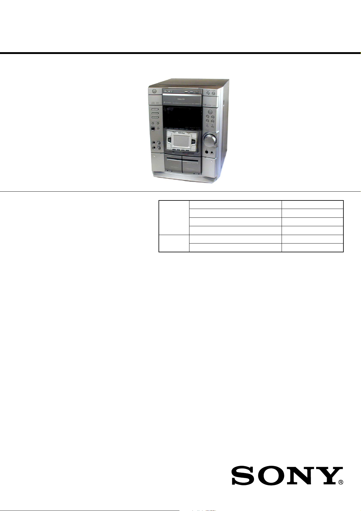
HCD-VP800AV
SERVICE MANUAL
Ver 1.3 2002.08
• HCD-VP800A V is the tuner, deck,
CD and amplifier section in MHCVP800AV.
Model Name Using Similar Mechanism HCD-VP700
CD CD Mechanism Type CDM58E-30BD61A
Section Base Unit Name BU-30BD61A
Optical Pick-up Name A-MAX.3
Tape deck Model Name Using Similar Mechanism HCD-VP700
Section T ape Transport Mechanism T ype TCM-230MWR41/AWR41
E Model
Tourist Model
SPECIFICATIONS
Amplifier section
The following measured at AC 120, 220, 240 V,
50/60 Hz
DIN power output (rated) 90 + 90 watts
(8 ohms at 1 kHz, DIN)
Continuous RMS power output (reference)
Front speaker: 120 + 120 watts
Center speaker: 40 watts
Rear speakers: 40 + 40 watts
(8 ohms at 1 kHz, 10%
THD)
Inputs
GAME IN: voltage 250 mV,
(phono jacks) impedance 47 kilohms
MD/VIDEO IN: voltage 450 mV/250 mV,
(phono jacks) impedance 47 kilohms
OPTICAL IN:
(Square optical connector jacks, front and rear panels)
wavelength ——
MIC 1/2: sensitivity 1 mV,
(phone jack) impedance 10 kilohms
Outputs
MD (VIDEO) OUT: voltage 250 mV
(phono jacks) impedance 1 kilohms
VIDEO OUT: max. output level
(phono jack) 1 Vp-p, unbalanced,Sync
S-VIDEO OUT: Y: 1 Vp-p, unbalanced,
(4-pin/mini-DIN jack) Sync negative,
PHONES: accepts headphones of
(stereo mini jack) 8 ohms or more
FRONT SPEAKER:
REAR SPEAKER:
CENTER SPEAKER:
SUB WOOFER:
negative, load impedance
75 ohms
C: 0.286Vp-p,
load impedance 75 ohms
accepts impedance of 8 to
16 ohms
accepts impedance of 8 to
16 ohms
accepts impedance of 8 to
16 ohms
Voltage 1 V,
impedance 1 kilohms
— Continued on next page —
9-873-195-04
2002H0200-1
© 2002. 08
MINI HI-FI COMPONENT SYSTEM
Sony Corporation
Home Audio Company
Published by Sony Engineering Corporation
HCD-VP800AV
VIDEO CD/CD player section
System Compact disc and digital
audio system
Laser Semiconductor laser
(λ=660 nm)
Frequency response 2 Hz – 20 kHz (±0.5 dB)
Signal-to-noise ratio More than 90 dB
Dynamic range More than 90 dB
Video color system format
NTSC, PAL
DIGITAL OUT OPTICAL
(Square optical connector jack, rear panel)
wavelength 660 nm
Tape player section
Recording system 4-track 2-channel stereo
Frequency response 40 – 13,000 Hz (±3 dB),
(DOLBY NR OFF) using Sony TYPE I
cassette,
40 – 14,000 Hz (±3 dB),
using Sony TYPE II
cassette
Tuner section
FM stereo, FM/AM superheterodyne tuner
FM tuner section
Tuning range
Tourist model: 76.0 – 108.0 MHz
Other models: 87.5 – 108.0 MHz
Antenna FM lead antenna
Antenna terminals 75 ohm unbalanced
Intermediate frequency 10.7 MHz
SAFETY-RELATED COMPONENT WARNING!!
COMPONENTS IDENTIFIED BY MARK 0 OR DOTTED LINE WITH
MARK 0 ON THE SCHEMATIC DIAGRAMS AND IN THE PARTS
LIST ARE CRITICAL TO SAFE OPERATION. REPLACE THESE
COMPONENTS WITH SONY PARTS WHOSE PART NUMBERS
APPEAR AS SHOWN IN THIS MANUAL OR IN SUPPLEMENTS
PUBLISHED BY SONY.
NOTES ON HANDLING THE OPTICAL PICK-UP
BLOCK OR BASE UNIT
The laser diode in the optical pick-up block may suffer electrostatic
break-down because of the potential difference generated by the
charged electrostatic load, etc. on clothing and the human body.
During repair, pay attention to electrostatic break-down and also
use the procedure in the printed matter which is included in the
repair parts.
The flexible board is easily damaged and should be handled with
care.
NOTES ON LASER DIODE EMISSION CHECK
The laser beam on this model is concentrated so as to be focused on
the disc reflective surface by the objective lens in the optical pickup block. Therefore, when checking the laser diode emission,
observe from more than 30 cm away from the objective lens.
Laser component in this product is capable
of emitting radiation exceeding the limit for
Class 1.
AM tuner section
Tuning range
Other models: 531 – 1,602 kHz
(with the interval set at
9 kHz)
530 – 1,710 kHz
(with the interval set at
10 kHz)
Antenna AM loop antenna
Antenna terminals External antenna terminal
Intermediate frequency 450 kHz
General
Power requirements
Thailand model: 220 V AC, 50/60 Hz
Other models: 120 V, 220 V or
230 – 240 V AC,
50/60 Hz
Adjustable with voltage
selector
Power consumption:
Dimensions (w/h/d)
Mass
225 watts
Approx. 280 x 360 x 365 mm
Approx. 12.0 kg
Supplied accessories: AM loop antenna (1)
FM lead antenna (1)
Remote commander (1)
Batteries (2)
Video cable (1)
Front speaker pads (8)
Center and rear speaker
pads (
12)
Design and specifications are subject to change
without notice.
This appliance is classified as a CLASS 1 LASER product. The
CLASS 1 LASER PRODUCT MARKING is located on the rear
exterior.
CAUTION
Use of controls or adjustments or performance of procedures
other than those specified herein may result in hazardous radiation
exposure.
Notes on chip component replacement
• Never reuse a disconnected chip component.
• Notice that the minus side of a tantalum capacitor may be
damaged by heat.
Flexible Circuit Board Repairing
• Keep the temperature of soldering iron around 270˚C
during repairing.
• Do not touch the soldering iron on the same conductor of the
circuit board (within 3 times).
• Be careful not to apply force on the conductor when soldering
or unsoldering.
2

TABLE OF CONTENTS
1. GENERAL ·········································································· 4
2. DISASSEMBY ··································································· 6
3. TEST MODE ···································································· 13
4. MECHANICAL ADJUSTMENTS ····························· 16
5. ELECTRICAL ADJUSTMENTS ······························· 16
6. DIAGRAMS
6-1. Circuit Board Location ················································ 23
6-2. Block Diagrams ··························································· 24
6-3. Printed Wiring Board – Driver Section –···················· 27
6-4. Schematic Diagram – Driver Section – ······················ 27
6-5. Schematic Diagram – BD Section – ···························· 28
6-6. Printed Wiring Board – BD Section – ························· 29
6-7. Printed Wiring Board – Main Section – ······················ 30
6-8. Schematic Diagram – Main Section (1/3) – ················ 31
6-9. Schematic Diagram – Main Section (2/3) – ················ 32
6-10. Schematic Diagram – Main Section (3/3) – ················ 33
6-11. Printed Wiring Board – DSP Section – ······················· 34
6-12. Schematic Diagram – DSP Section (1/2) – ················· 35
6-13. Schematic Diagram – DSP Section (2/2) – ················· 36
6-14. Printed Wiring Board – OPT Section – ······················· 37
6-15. Schematic Diagram – OPT Section – ························· 37
6-16. Printed Wiring Board – Front Amp Section –············· 38
6-17. Schematic Diagram – Front Amp Section – ··············· 39
6-18. Printed Wiring Board – Surround Amp Section – ······ 40
6-19. Schematic Diagram – Surround Amp Section – ········· 41
6-20. Printed Wiring Board – Panel Section – ····················· 42
6-21. Schematic Diagram – Panel Section (1/2) – ··············· 43
6-22. Schematic Diagram – Panel Section (2/2) – ··············· 44
6-23. Printed Wiring Board – Leaf SW Section – ················ 45
6-24. Schematic Diagram – Leaf SW Section – ··················· 45
6-25. Printed Wiring Board – Video Section –····················· 46
6-26. Schematic Diagram – Video Section (1/3) – ··············· 47
6-27. Schematic Diagram – Video Section (2/3) – ··············· 48
6-28. Schematic Diagram – Video Section (3/3) – ··············· 49
6-29. Printed Wiring Board – Trans Section – ····················· 50
6-30. Schematic Diagram – Trans Section – ························ 51
6-31. IC Pin Function Description ······································· 52
6-32. IC Block Diagrams ····················································· 60
HCD-VP800AV
7. EXPLODED VIEWS
7-1. Main Section ································································· 64
7-2. Front Panel Section ······················································· 65
7-3. Chassis Section ····························································· 66
7-4. Tape Mechanism Deck Section-1 (TCM-230MWR41) 67
7-5. Tape Mechanism Deck Section-2 (TCM-230AWR41) 68
7-6. CD Mechanism Deck Section (CDM58E-30BD61A) ·· 69
7-7. Base Unit Section (BU-30BD61A) ······························ 70
8. ELECTRICAL PARTS LIST ······································· 71
3
HCD-VP800AV
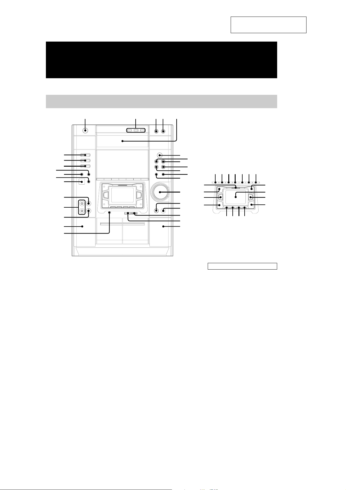
Parts Identification
The items are arranged in alphabetical order.
Main unit
SECTION 1
GENERAL
12345
This section is extracted from
instruction manual.
e;
wl
wk
wj
wh
wg
wf
wd
ws
wa
w;
ql
2CH/MULTI rs (27)
CD e; (9, 12–15, 22, 23)
CD SYNC HI-DUB qj (22, 23)
CLOCK/TIMER SET ed (11, 23,
29)
DECK A Z w; (21)
DECK B Z qk (21)
digipad el (6, 10, 11, 13, 15,
19–21, 24, 26, 30)
DIGITAL wh (31)
DIGITAL IN 2 (OPTICAL) jack
wf (31)
DIRECTION eg (21–23, 28)
DISC 1–3 2 (12–15, 23)
DISC SKIP EX-CHANGE 3
(12–14)
Disc tray 5 (12)
DISPLAY ea (11, 16)
DOLBY NR eh (21–23)
DSP EDIT rj (25)
ECHO LEVEL control wd (28)
EDIT eg (23)
EFFECT rd (25, 26)
ENTER r; (11, 14, 15, 19, 20,
23, 24, 26, 29, 30)
6
7
8
9
q;
qa
qs
qd
qf
qg
qh
qj
qk
FM MODE eh (20)
GAME wg (31)
GAME MODE rh (25)
GROOVE rf (25)
IR receptor qf
KARAOKE PON es (27, 28)
MD (VIDEO) wj (31)
MIC 1/2 jack ws (27, 28)
MIC LEVEL control wa (27, 28)
MOVIE MODE ek (25)
MULTI CHANNEL DECODING
indicator rl (29)
MUSIC MODE rk (25)
P FILE rg (26)
PICTURE EFFECT ql (19)
PHONES jack qg
PLAY MODE ej (12, 14, 15, 23)
REC/PAUSE START qh (22, 23,
28)
REPEAT eh (13, 15)
TAPE A/B wk (21, 22)
TIMER SELECT ef (24, 30)
TOOL MODE ra (25)
TUNER/BAND wl (20)
TUNER MEMORY ej (20)
VOLUME control qd
eaesedefegeh
rl
rk
rj
rh
rfrdrs
rg
BUTTON DESCRIPTIONS
@/1 (power) 1
Z OPEN/CLOSE (disc tray) 4
nN (play) 6
X (pause) 7
x (stop) 8
. (go back) q;
> (go forward) 9
m/– (rewind) qs
M/+ (fast forward) qa
ej
ek
el
r;
ra
4

Setting the time
1 Turn on the system.
2 Press CLOCK/TIMER SET.
When you set the time for the first time,
proceed to step 5.
3 Press . or > repeatedly to select
“CLOCK SET”.
4 Press ENTER.
5 Press . or > repeatedly to set the
hour.
6 Press ENTER.
7 Press . or > repeatedly to set the
minutes.
8 Press ENTER.
Tips
• If you have made a mistake or want to change the
time, start over from step 2.
• You can use the digipad instead of ./>.
Note
The clock settings are canceled when you disconnect
the power cord or if a power failure occurs.
HCD-VP800AV
5
HCD-VP800AV
)
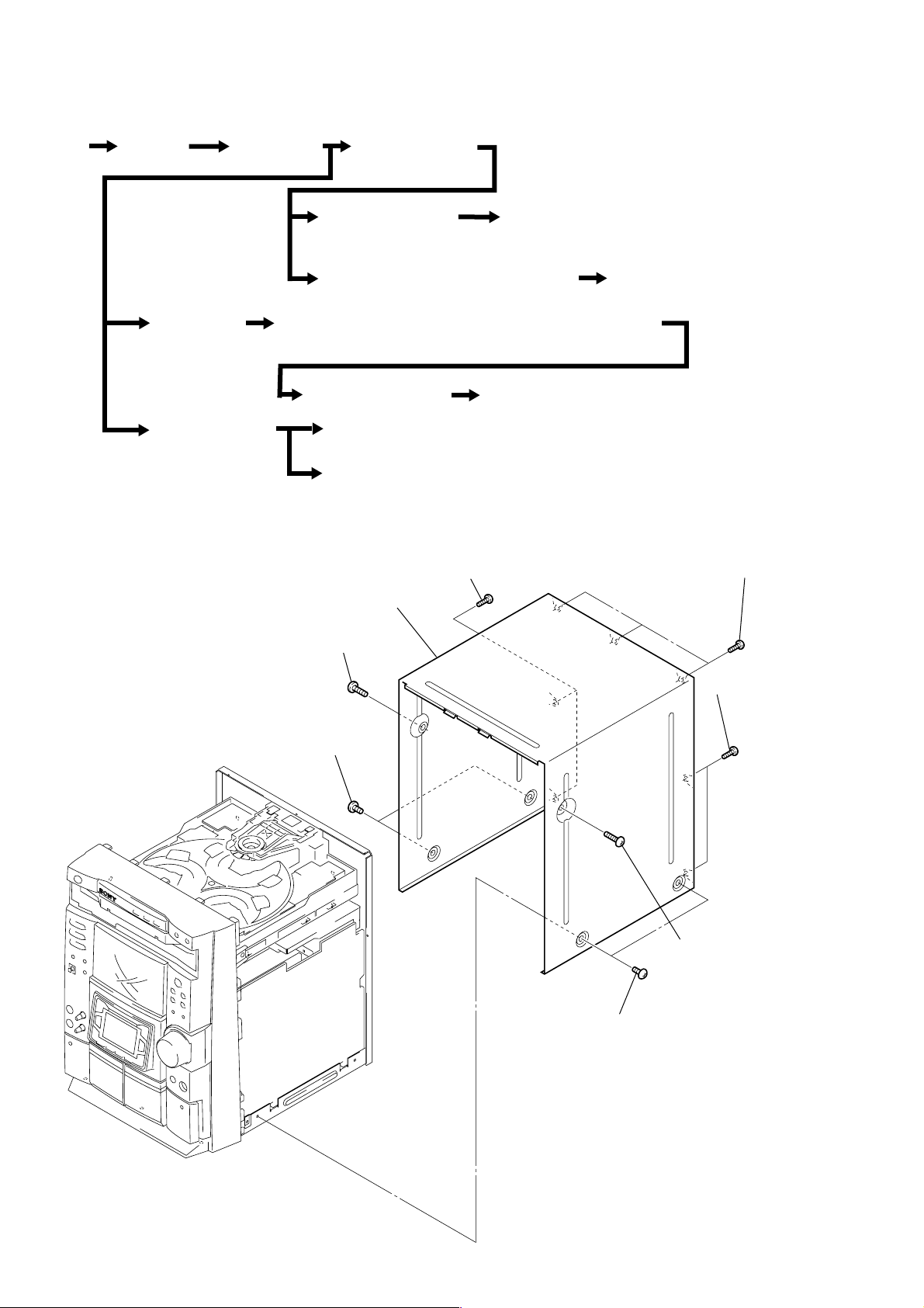
SECTION 2
DISASSEMBLY
• The equipment can be removed using the following procedure.
Set Case (Top) Loading Panel Front Panel Section
Tape Mechanism Deck
(TCM-230AWR41/MWR41)
CD Panel board, Panel board, OPT IN Board
Chassis section
DSP board, SUB Trans board, Back panel, Fan, OPT IN rear board
Tnans board, Main board
CD mechanism deck
(CDM58)
Base unit, BD board
(BU-30BD61A)
Driver board, Motor board, CD sensor board, Video board
Note : Follow the disassembly procedure in the numerical order given.
2-1. CASE (TOP)
• Abbreviation
SP : Singapre model
MY : Malaysia model
TH : Thai model
LEAF SW board, Head (A) board,
Head (B) board
Escutcheon pad
(With touch pad)
Front AMP board, Surround AMP board
4
screw (case 3 TP2)
3
two screws (case 3 TP2)
8
5
two screws (+BVTT 3
case
×
6
8)
three screws (+BVTT 3
7
two screws
(+BVTT 3
2
screw (case 3 TP2)
1
two screws (case 3 TP2)
×
8)
×
8
6
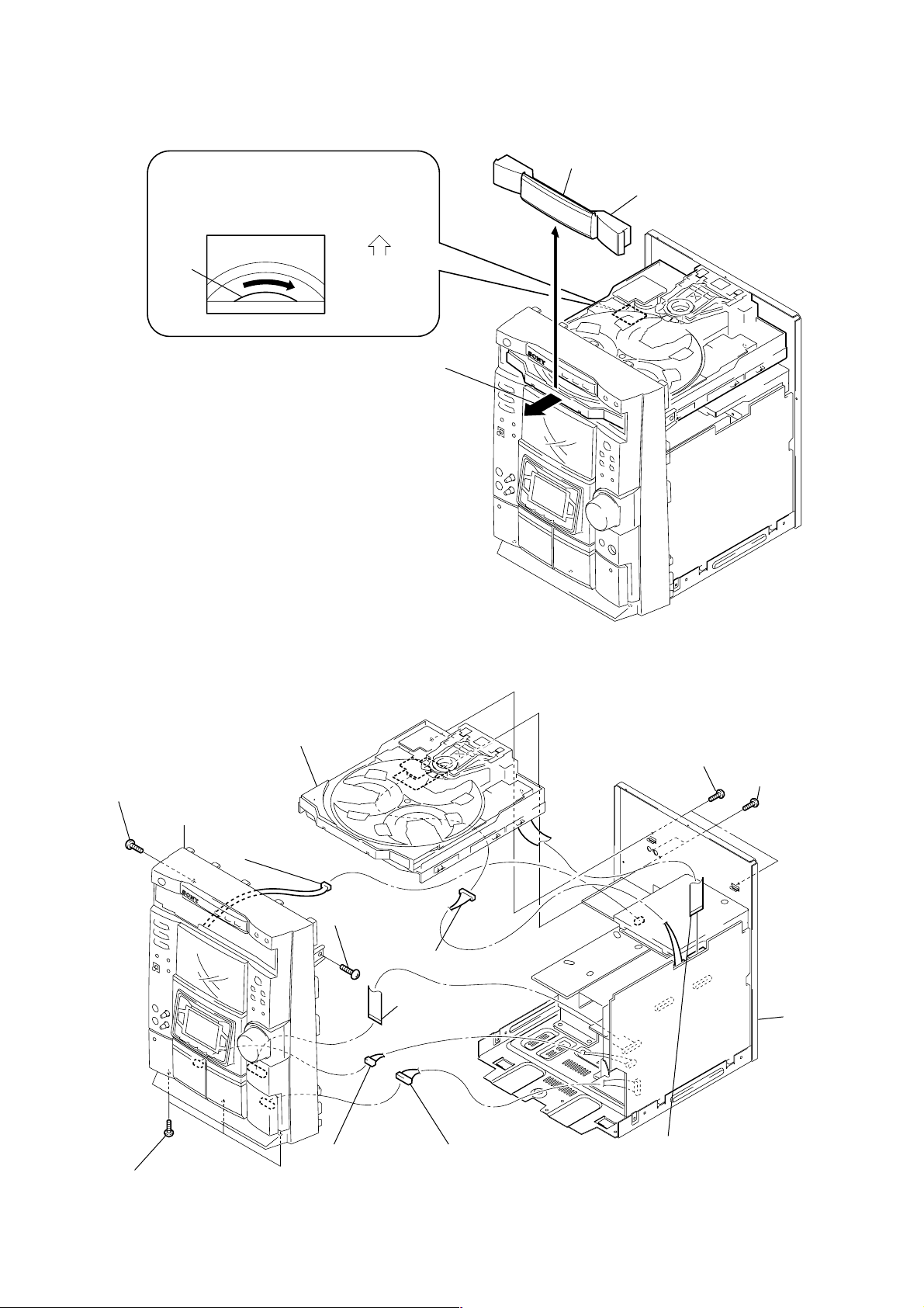
2-2. LOADING PANEL
CD mechanism deck (CDM58)
1
turn the pulley to the direction of arrow.
front panel side
4
pull-out the disc tray.
loading panel
HCD-VP800AV
pulley
2
pull-out the disc tray.
3
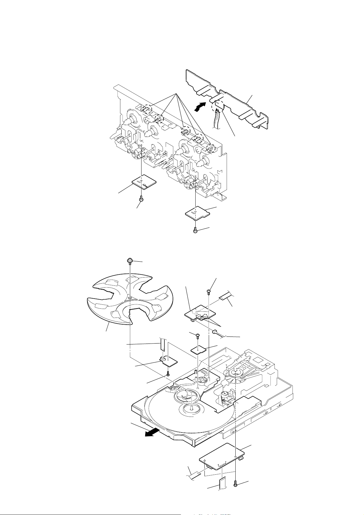
2-3. FRONT PANEL SECTION, CHASSIS SECTION, CD MECHANISM DECK (CDM58)
qd
3
screw (+BVTP 3
5
front panel section
4
three screws (+BVTT 3
CD mechanism deck (CDM58)
×
10)
1
connector (CN601)
2
screw
(+BVTP 3
7
connector (CN1)
×
8)
×
10)
qs
connector (CN701)
6
flat type wire (CN1001)
8
connector (CN2)
0
two screws (+BVTP 3
9
flat type wire (CN201)
× 10
)
qa
two screws
(+BVTP 3
chassis section
× 10
)
7
HCD-VP800AV
)
)
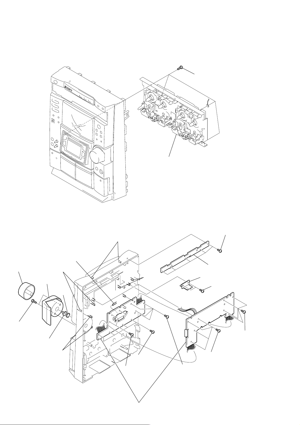
2-4. TAPE MECHANISM DECK (TCM-230AWR41/MWR41)
1
four screws (+BVTP 2.6
2
tape mechanism deck
(TCM-230AWR41/MWR41)
×
8
2-5. CD PANEL BOARD, PANEL BOARD, OPT IN BOARD
two claws
qf
flat type wire (CN108)
5
ring (vol)
×
8)
6
cover(vol)
two claws
two claws
7
nut
qa
five screws
(+BVTP 2.6
0
three
screws
(+BVTP 2.6
3
knob (vol)
4
two screws
(+BVTP 2.6
two claws
×
8)
×
1
five screws
(+BVTP 2.6
2
CD panel board
qh
OPT IN board
qg
two screws
(+BVTP 2.6
8
four screws
(+BVTP 2.6
9
five screws
8)
qs
four screws
(+BVTP 2.6
(+BVTP 2.6
×
8)
×
×
×
8)
8)
×
8
8)
qd
PANEL board
8
2-6. ESCUTCHEON PAD (WITH TOUCH PAD)
)
1
button (edit)
3
two screws
(+BVTP 2.6
touch pad
7
holder (pad)
6
two screws
(TPG +P 2
×
8)
×
8)
5
two screws
(TPG +P 2
4
escutcheon (pad)
HCD-VP800AV
8
three screws
(+BVTP 2.6
2
two screws
(+BVTP 2.6
×
8)
9
button (DSP
×
8)
×
8)
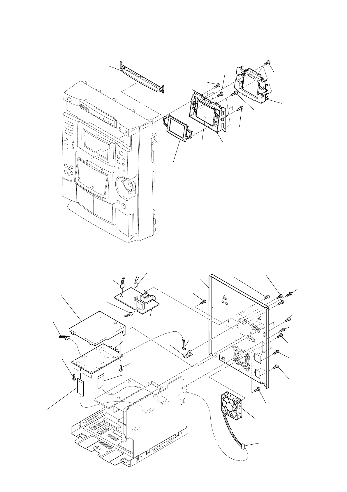
2-7. DSP BOARD, SUB TRANS BOARD, BACK PANEL, FAN, OPT IN REAR BOARD
1
two screws
(+BVTP 3
×
8)
wg
qf
connector (CN902)
0
bracket (DSP)
7
connector
(CN601)
9
two screws
(+BVTP 3
5
flat type wire (CN602)
×
8)
qg
connector
(CN903)
qd
connector (CN901)
qh
SUB trans board
qa
DSP
board
8
two screws
(+BVTP 3
4
flat type wire (CN603)
×
ws
wa
screw
(+BVTP 3
OPT IN
rear board
8)
back panel
×
6
connector
(CN801)
8)
qs
two screws
(+BVTP 3
×
w;
rew (+BVTP 3
fan
8)
wh
(+BVTP 3
3
(+BVTP 3
qj
(+BVTP 3
wf
(+BVTP 3
qk
(+BVTP 3
ql
(+BVTP 3
screw
four screws
2
(+BVTP 3
two screws
×
two screws
two screws
two screws
two screws
×
8)
×
8)
8)
×
8)
×
8)
×
10
)
×
8)
×
8)
wd
connector
(CN104)
9
HCD-VP800AV
)
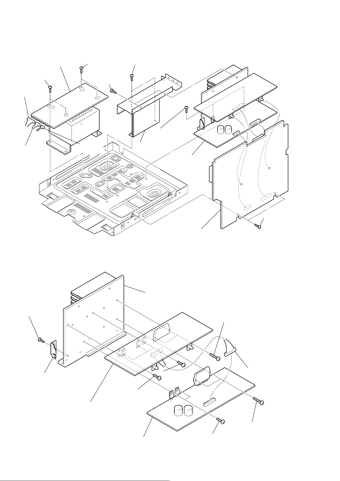
2-8. TRANS BOARD, MAIN BOARD
4
6
5
two screws
(+BVTT 4
1
connector
(CN914)
2
connector
(CN915)
TRANS board
×
8)
two screws
(+BVTT 4
7
two screws
(+BVTT 3
3
connector
(CN913)
×
8
two screws
×
8)
(+BVTP 3
9
8)
×
8)
0
two
screws
(+BVTP 3
cover (heat sink)
qa
SURROUND and
FRONT AMP
board ASSY
×
8)
2-9. FRONT AMP BOARD, SURROUND AMP BOARD
heat sink assy
1
screw
(+BVTT 3
2
bracket
×
8)
qd
8
t
hree screws
(+BVTT 3
MAIN board
×
8)
9
two
screws
(+BVTP 3
qs
two
(+BVTP 3
×
16)
3
connector (CN803
screws
×
8)
10
0
SURROUND AMP board
7
screw
(+BVTT 3
6
FRONT AMP board
×
8)
5
two
screws
(+BVTP 3
4
two
screws
(+BVTT 3
×
8)
×
16)
HCD-VP800AV
2-10. LEAF SW BOARD, HEAD (A) BOARD, HEAD (B) BOARD (TCM-230AWR41/MWR41)
Note: This illustration is for TCM-230MWR, but in case of TCM-230AWR, you can remove them in the same way.
1
five claws
2
LEAF SW board
3
remove the four solderings.
5
HEAD (A) board
6
4
screw (+PTT 2
ground point
×
4),
HEAD (B) board
4
screw (+PTT 2
ground point
×
4),
2-11. DRIVER BOARD, MOTOR BOARD, CD SENSOR BOARD, VIDEO BOARD
q;
qa
Tray
3
Flat type wire
(CN702)
2
DRIVER board
Screw (+PTPWH 2.6
qs
Screw (+BVTP 2.6
8
×
8)
4
MOTOR board
×
8)
Two screws (+BVTP 2.6
6
Flat type wire (CN721)
5
Remove the two solderings of motor.
7
Connector (CN722)
qd
CD SENSOR board
×
8)
1
Screw (+BVTP 2.6
9
Pull-out the Table.
×
8)
qf
Flat type wire (CN502)
qg
Flat type wire (CN501)
qj
VIDEO board
qh
Tw o
Screws
(+BVTP 2.6
×
8)
11
HCD-VP800AV
)
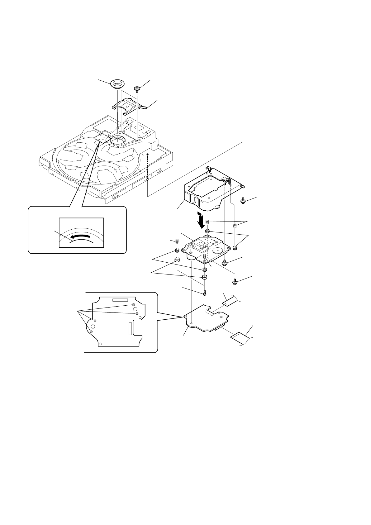
2-12. BASE UNIT, BD BOARD
1
Pulley(B)(BU-30), chucking
2
Tw o
Screws (+PTPWH M2.6)
3
Lever (lifter)
5
Screw (+PTPWH M2.6)
4
Turn the pulley to the direction of arrow.
pulley
9
Remove the solder
(four portions).
6
Spring (insulator),
coil
qh
Two insulators
qs
Two stoppers
qa
Two screws (+BVTP 2.6
Holder assy
Base unit
×
8)
q;
BD board
qg
Spring
(insulator),
coil
8
Flat type wire (CN102)
7
Spring (insulator), coil
qh
Two insulators
qf
Screw (DIA. 12)
qd
Tw o
screws (+PTPWH M2.6
Flat type wire (CN101)
12

SECTION 3
TEST MODE
HCD-VP800AV
[Cold Reset]
• The cold reset clears all data including preset data stored in the
RAM to initial conditions. Execute this mode when returning
the set to the customer.
Procedure:
1. Press three buttons x , DISPLAY , and DISC 1
simultaneously.
2. The fluorescent indicator tube becomes blank instantaneously,
and the set is reset.
[Tuner Step Change] (Except for European and Middle Eastern
models)
• A step of AM channels can be changed over between 9 kHz and
10 kHz.
Procedure:
1. Press `/1 button to turn the set ON.
2. Select the function “TUNER”, and press TUNER/BAND button
to select the BAND “AM”.
3. Press `/1 button to turn the set OFF.
4. Press ENTER and `/1 buttons simultaneously, and the
display of fluorescent indicator tube changes to “AM 9 k ST”
or “AM 10 k ST”, and thus the channel step is changed over.
[GC Test Mode]
• This mode is used to check the software version, FL tube, LED,
keyboard and VACS.
Procedure:
1. Press three buttons x , DISPLAY , and DISC 2
simultaneously.
2. LEDs and fluorescent indicator tube are all turned on.
3. When you want to enter the software version display mode,
press DISC 1 .The model number and destination are displayed.
4. Each time DISC 1 is pressed, the display changes stating from
MC version, GC version, CD version, CDD, CDM version BD,
ST version, TA version, TM version, TC version, in this order,
and returns to the model number and destination display.
5. When DISC 3 is pressed while the version numbers are being
displayed except model number and destination, year, month
and day of the software creation appear. When DISC 3 is pressed
again, the display returns to the software version display. When
DISC 1 is pressed while year, month and day of the software
creation are being displayed, the year, month and day of creation
of the software versions are displayed in the same order of
version display.
6. Press DISC 2 button, and the key check mode is activated.
7. In the key check mode, the fluorescent indicator tube displays
“KOJOVO”. Each time a button is pressed, “KEY” value
increases.
However, once a button is pressed, _it is no longer taken into
account.
“VOL” value increases like 1, 2, 3...if rotating VOLUME knob
in “+” direction, or it decreases like 0, 9, 8...if rotating in
“_”direction.
8. Also when DISC 3 is pressed after lighting of all LEDs and FL
tubes, value of VACS appears.
9. To exit from this mode, press three buttons in the same manner
as step 1, or disconnect the power cord.
[MC Test Mode]
• This mode is used to check operations of the respective sections
of Amplifier, Tuner, and Tape.
Procedure:
• To enter MC Test Mode
1. Press the `/1 button to turn on the set.
2. Press the three buttons of x , DISPLAY and DISC 3
simultaneously.
3. Cursor segment flash on the FL display tube. The input
FUNCTION is changed to GAME.
* Check of Amplifier
Initial settings: Input , GAME
EQ , FLAT
Mode , MUSIC
VA C S , OFF
Output channel switching:
MUSIC key: L , LR , R through
MOVIE key: L , SL R , SR through
GAME key:L , L, SL, C R , R, SR, SW through
TOOL MODE key: L , CR , SW through
1. When the VOLUME control knob is turned clockwise even
slightly, the sound volume increases to is maximum and a
message “VOLUME MAX” appears for two seconds, then the
display returns to the original display.
2. When the VOLUME control knob is tuned counter-clockwise
even slightly, the sound volume decreases to its minimum and a
message “VOLUME MIN” appears for two seconds, then the
display returns to the original display.
* Tuner function
1. In the test mode, the default-preset channel is called even when
the TUNER is selected and an attempt is made to call the preset
channel that has been stored in memory. (It means that the
memory is cleared.)
2. The minimum, center and maximum frequency of each band is
set then.
* Tape recording test
1. To enter the MC Test Mode.
2. Load tapes in both tape decks A and B.
3. Press the REC button to start recording.
4. Pressing the M , m buttons during recording returns the
tape to the recording start position and stops it at this position.
5. Pressing the “High Speed Dubbing” key while playing back the
tape of deck B switches the playback speed between “Normal
Speed” and “High Speed”.
Note:
When the playback direction of the tape is set to other than “ONY
WAY”, the restriction on the number of times playback which can
be repeated will be cleared.
* AMS Test Mode
1. Set TAPE function
2. Select the desired loop by pressing the PLAY MODE button.
Insert a test tape AMS-110A or AMS-120 to Deck A.
3. Press the SPECTRUM or KARAOKE PON button to enter
the AMS test mode.
4. After a tape is rewound first, the FF AMS is checked, and the
mechanism is shut off after detecting the AMS signal the AMS
signal twice.
5. Then the REW AMS is checked and the mechanism is shut off
after detecting the AMS signal twice.
6. When the check is complete, a message of either OK or NG
appears.
* To return to normal mode again.
1. When you want to exit this mode, press the `/1 button.
2. The cold reset is enforced at the same time.
13

HCD-VP800AV
[CD Ship Mode (No Memory Clear)]
• This mode moves the position to the position durable to vibration Use this mode when returning the set to the customer after
repair.
Procedure:
1. Press `/1 button to turn the set ON.
2. Press three ENTER , DISK 1 button and CD button
simultaneously.
3. After the “STANBY” display blinks six times, a message
“LOCK” is displayed on the fluorescent indicator rube, and the
CD ship mode is set.
[CD Ship Mode (Memory Clear)]
• This mode moves the pickup to the position durable to vibration. Use this mode when returning the set to the customer after
repair.
Procedure:
1. Press
2. Press three buttons CD and
3. After the “STANDBY” display blinks six times, a message
“LOCK” is displayed on the fluorescent indicator tube, and the
CD ship mode is set.
button to turn the set ON.
`/1
button simultaneously.
`/1
[CD Service Mode]
• This mode can run the CD sled motor freely. Use this mode, for
instance, when cleaning the pickup.
Procedure:
1. Press
2. Select the function “CD”.
3. Press three buttons ENTER , DISC 1 , and x simultaneously.
4. The CD service mode is selected.
5. With the CD in stop status, press M button to move the
pickup to outside track, or press m button to inside track.
6. To exit from this mode, perform as follows:
1) Move the pickup to the most inside track.
2) Press
Note:
• Always move the pickup to most inside track when exiting from
this mode. Otherwise, a disc will not be unloaded.
• Do not run the sled motor excessively, otherwise the gear can
be chipped.
button to turn the set ON.
`/1
button to turn the set OFF.
`/1
14
HCD-VP800AV
[VCD COLOR SYSTEM MODE]
• This mode is used for changing the COLOR SYSTEM of the
VCD.
Procedure:
1. Set the standby mode.
2-1.Press the two buttons
`/1
and
simultaneously to set the
>
COLOR SYSTEM of the VCD to AUTO.
2-2.Press the two buttons
`/1
and
simultaneously to fix the
.
COLOR SYSTEM of the VCD to PAL.
2-3.Press the two buttons
and X simultaneously to fix the
`/1
COLOR SYSTEM of the VCD to NTSC.
3. The power tune ON automatically and the function sets to“CD’’.
4. The FL tube shows the COLOR SYSTEM mode see .
5. The COLOR SYSTEM mode set is maintained (memorized)
until COLD RESET is executed.
[VIDEO CD Color-bars Mode]
On this mode, the data of the color-bars signal as a picture signal
and the 1 kHz sine wave signal as a sound signal are output by the
mechanism controller (IC502) for the video CD signal check. When
measurement of the voltage and waveform on the VIDEO board,
perform it in this mode.
For reference, the color-bars signal can be observed at J302 using
an oscilloscope.
Procedure:
1. Short the both ends of the land of SL503 of the VIDEO board.
2. Turn the power on. Press the CD button to select CD.
3. The color-bars appears when the CD is in stop status, and it
disappears when the CD goes in play status.
4. After measuring, remove the lead wire connected.VIDEO board
(SIDE B)
[VIDEO BOARD] (SIDE A)
J301
CN501
SL503
SL502
SL501
CHECK LED
CN502
1 2 3
J302
CN503
[CD Servo ON/OFF Mode]
Procedure:
1. Short SL502 on the VIDEO board by soldering.
2. Turn on the main power. Set a disc on the DISC1 tray. Select
CD.
3. Press the hH button to play back CD.
4. When the > button is pressed, 100 track jump is executed.
5. Also, every pressing of the PLAY MODE button triggers
between ON and OFF of TRACKING SERVO and SLED
SERVO.
How to quit the CD servo ON/OFF mode:
1. Press the ?/1 button to turn off the main power.
2. Remove soldering from SL502.
[REPEAT 5 LIMIT OFF MODE]
• This mode is used to enable infinite repetitions.
Normally, the number of repetitions allowed is 5.
Procedure:
1. Press the
button to turn ON the power supply.
`/1
2. Set the function “CD”.
3. Press the three burtons ENTER , DISC 3 , and x is
simultaneously.
4. Infinite repetitions is enabled.
5. This state is maintained ( memorized ) until COLD RESET is
executed.
15
HCD-VP800AV
r
SECTION 4
MECHANICAL ADJUSTMENTS
SECTION 5
ELECTRICAL ADJUSTMENTS
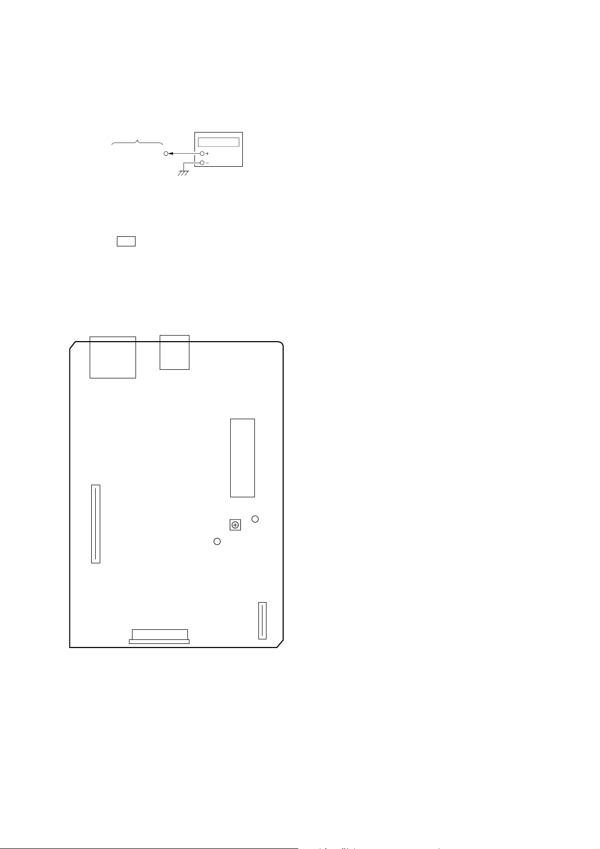
Precaution
1. Clean the following parts with a denatured alcohol-moistened
swab:
record/playback heads pinch rollers
erase head rubber belts
capstan idlers
2. Demagnetize the record/playback head with a head
demagnetizer.
3. Do not use a magnetized screwdriver for the adjustments.
4. After the adjustments, apply suitable locking compound to the
parts adjusted.
5. The adjustments should be performed with the rated power
supply voltage unless otherwise noted.
Torque Measurement
Mode
FWD
FWD
back tension
REV
REV
back tension
FF/REW
FWD tension
REV tension
Torque meter
CQ-102C
CQ-102C
CQ-102RC
CQ-102RC
CQ-201B
CQ-403A
CQ-403R
Meter reading
3.06 N • m to 6.96 N • m
31 to 71 g • cm
(0.43 – 0.98 oz • inch)
0.19 N • m to 0.58 N • m
2 to 6 g • cm
(0.02 – 0.08 oz • inch)
3.06 N • m to 6.96 N • m
31 to 71 g • cm
(0.43 – 0.98 oz • inch)
0.19 N • m to 0.58 N • m
2 to 6 g • cm
(0.02 – 0.08 oz • inch)
6.96 N • m to 14.02 N • m
71 to 143 g • cm
(0.98 – 1.99 oz • inch)
9.80 N • m
100 g or more
(3.53 oz or more)
9.80 N • m
100 g or more
(3.53 oz or more)
DECK SECTION
1. Demagnetize the record/playback head with a head
demagnetizer.
2. Do not use a magnetized screwdriver for the adjustments.
3. After the adjustments, apply suitable locking compound to the
parts adjust.
4. The adjustments should be performed with the rated power
supply voltage unless otherwise noted.
5. The adjustments should be performed in the order given in this
service manual. (As a general rule, playback circuit adjustment
should be completed before performing recording circuit
adjustment.)
6. The adjustments should be performed for both L-CH and RCH.
7. Switches and controls should be set as follows unless otherwise
specified.
• Test Tape
Tape Signal Used for
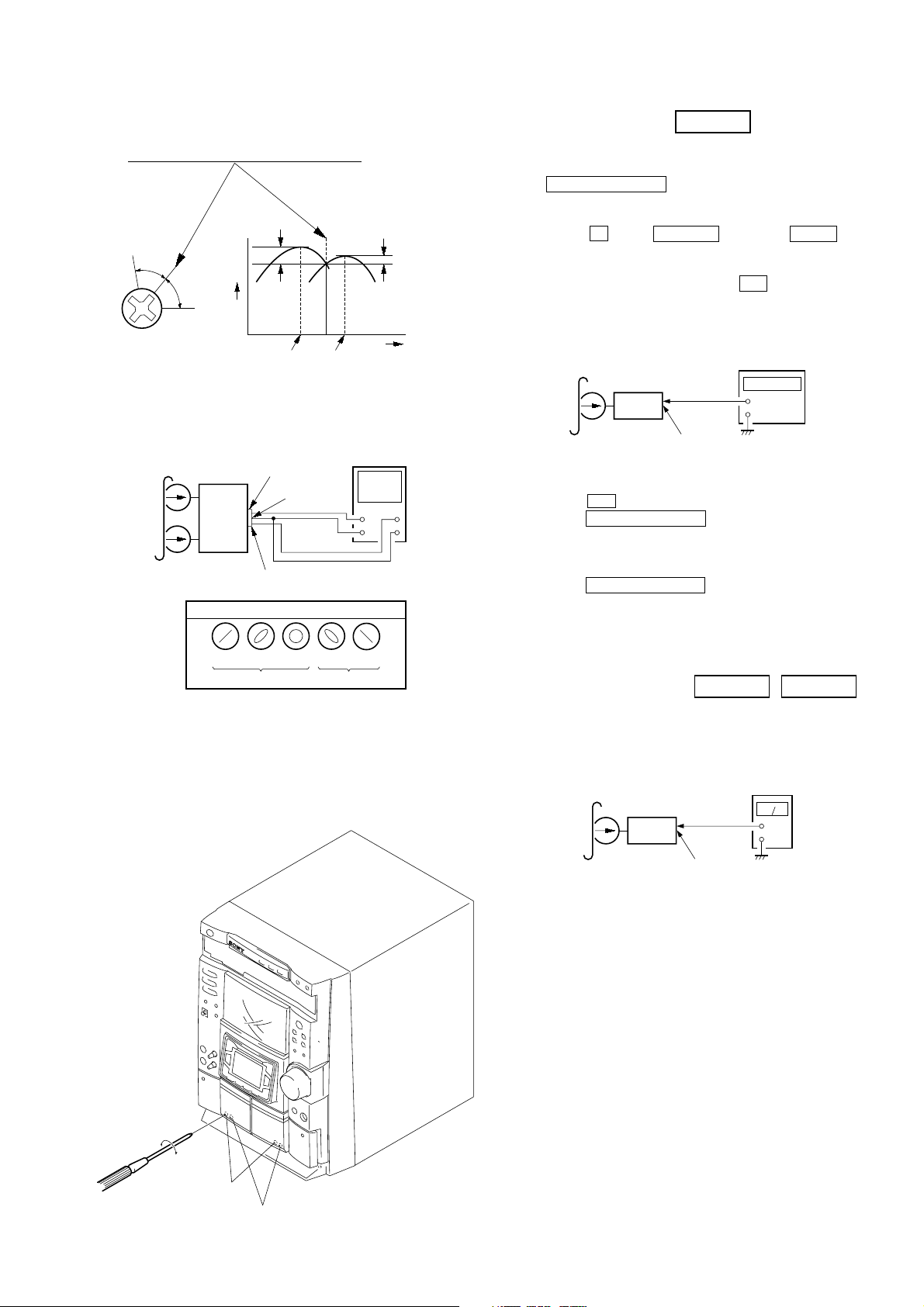
P-4-A100 10 kHz, –10 dB Azimuth Adjustment
WS-48B 3 kHz, 0 dB Tape Speed Adjustment
P-4-L300 315 Hz, 0 dB Level Adjustment
Record/Playback Head Azimuth Adjustment
0 dB=0.775 V
DECK A DECK B
Note: Perform this adjustments for both decks
Procedure:
1. Mode: Playback
test tape
P-4-A100
(10 kHz, –10 dB)
set
main board
CN301
Pin 3 (L-CH)
Pin 1 (R-CH)
main board
CN301
Pin 2 (GND)
level mete
+
–
16
HCD-VP800AV
e
+
–
set
test tape
P-4-L300
(315 Hz, 0 dB)
main board
CN301 (Pin 3 : L-CH)
(Pin 1 : R-CH)
level meter
2. Turn the adjustment screw and check output peaks. If the peaks
do not match for L-CH and R-CH, turn the adjustment screw
so that outputs match within 1dB of peak.
Output
level
within
1dB
L-CH
peak
R-CH
peak
within
1dB
Screw
position
L-CH
peak
Screw
position
R-CH
peak
3. Mode: Playback
test tape
P-4-A100
(10 kHz, –10 dB)
L-CH
MAIN
board
CN301
set
R-CH
waveform of oscilloscope
in phase 45 ° 90° 135° 180°
pin 3
pin 2
L
R
pin 1
good
oscilloscop
V
wrong
H
4. After the adjustments, apply suitable locking compound to the
pats adjusted.
Tape Speed Adjustment DECK B
Note: Start the Tape Speed adjustment as below after setting to the test
mode.
In the test mode, the tape speed is high during pressing the
CD SYNC HI-DUB button.
Procedure:
1. Turn the power switch on.
2. Press the x button, DISPLAY button and DISC 3 button
simultaneously.
(Cursor segment flash on the FL display tube.)
To exit from the test mode, press the ?/1 button.
Mode: Playback
test tape
WS-48B
(3 kHz, 0 dB)
set
main board
CN301 (Pin 3 : L-CH)
frequency counter
+
–
(Pin 1 : R-CH)
1. Insert the WS-48B into the deck B.
2. Press the Y button on the deck B.
3. Press the CD SYNC HI-DUB button in playback mode.
Then at HIGH speed mode.
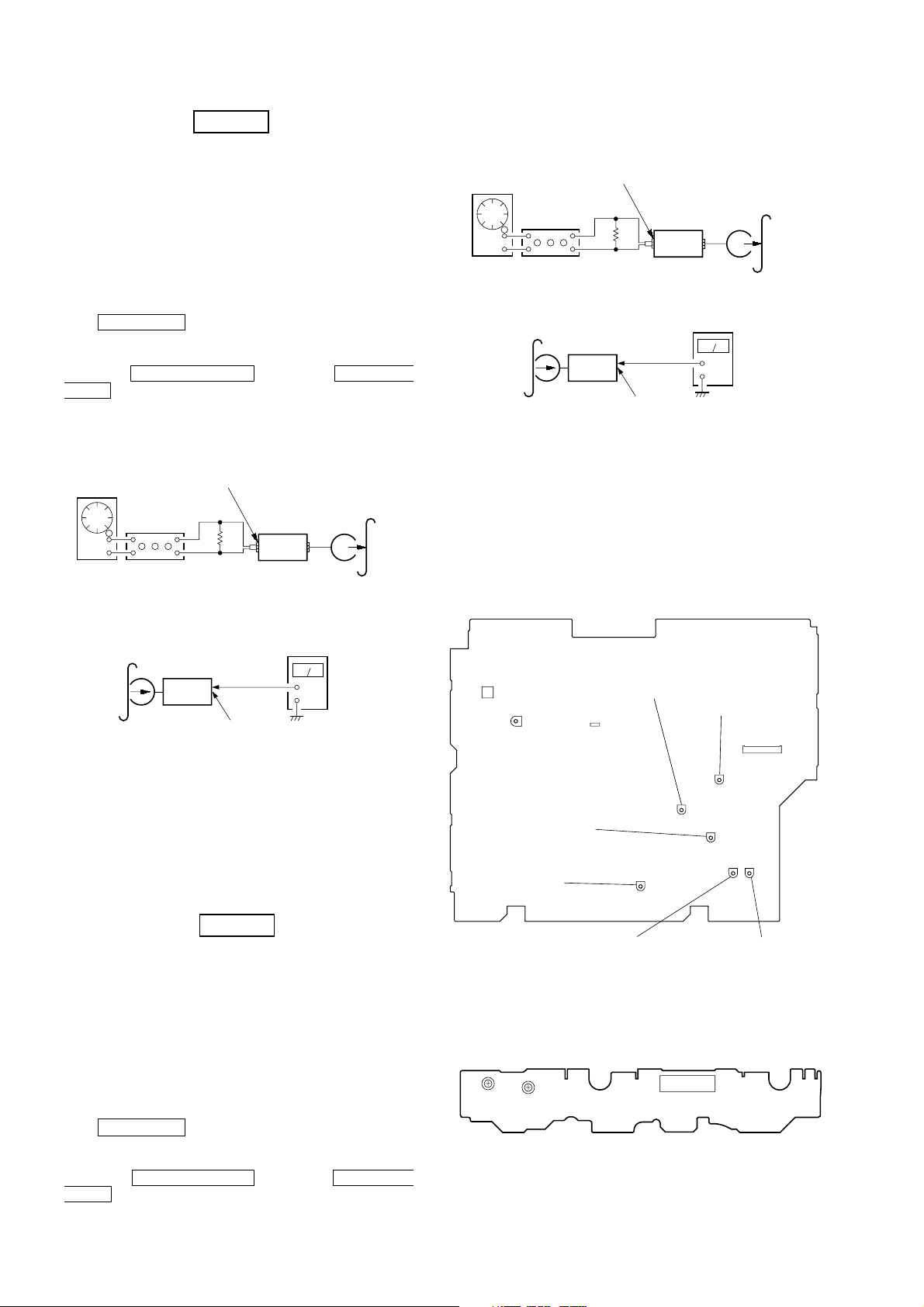
4. Adjust RV1001 on the LEAF SW board do that frequency
counter reads 6,000 ± 30 Hz.
5. Press the CD SYNC HI-DUB button.
Then back to NORMAL speed mode.
6. Adjust RV1002 on the LEAF SW board so that frequency
counter reads 3,000 ± 15 Hz.
Adjustment Location: LEAF SW board
Playback level Adjustment DECK A DECK B
Procedure:
Mode: Playback
Adjustment Location: Playback Head (Deck A).
Record/Playback/Erase Head (Deck B).
forward
reverse
Deck A is RV302 (L-CH), Deck B is RV303 (L-CH) so that
adjustment within adjustment level as follows.
Adjustment Level:
CN301 PB level: 334 to 375 mV (–6.8 dB ± 0.5 dB) level
difference between the channels: within ±0.5 dB
Adjustment Location: MAIN board
Sample Volue of Wow and Flutter: 0.3% or less W. RMS
(WS-48B)
17
HCD-VP800AV
r
REC Bias Adjustment DECK B
Procedure:
INTRODUCTION
When set to the test mode performed in Tape Speed Adjustment,
when the tape is rewound after recording, the “REC memory mode”
which rewinds only the recorded portion and playback is set.
This “REC memory mode” is convenient for performing this
adjustment. During recording, the input signal FUNCTION will
automatically switch to VIDEO.
(If do not operation of stopped from recording complete, and rotette
of shuttle knob then rewind to recording start position.)
1. Press MD (VIDEO) button to select VIDEO. (This step is not
necessary if the above test mode has already been set.)
2. Insert a tape into deck B.
3. After press REC PAUSE/START button, press REC PAUSE/
START button, then recording start.
4. Mode: Record
MD/VIDEO (AUDIO) IN
1) 315 Hz
2) 10 kHz
AF OSC
attenuator
50 mV (–23.8 dB)
600 Ω
set
blank tape
CN-123
4. Mode: Record
MD/VIDEO (AUDIO) IN
AF OSC
315 Hz, 50 mV (–23.8 dB)
600 Ω
attenuator
blank tape
CS-123
set
5. Mode: Playback
recorded
portion
set
CN301 (Pin 3 : L-CH)
(Pin 1 : R-CH)
level mete
+
–
6. Confirm playback the signal recorded in step 3 become
adjustable level as follows.
If these levels do not adjustable level, adjustment the RV301
(L-CH) and RV351 (R-CH) on the MAIN board to repeat steps
4 and 5.
Adjustable level:
CN301 PB level: 33.4 to 37.5 mV (–27.3 to –26.3 dB)
Adjustment Location: MAIN board
5. Mode: Playback
recorded
portion
set
CN301 (Pin 3 : L-CH)
(Pin 1 : R-CH)
level meter
+
–
6. Confirm playback the signal recorded in step 3 become
adjustable level as follows.
If these levels do not adjustable level, adjustment the RV304
(L-CH) and RV354 (R-CH) on the AUDIO board to repeat steps
4 and 5.
Adjustable level: Playback output of 315 Hz to playback output
of 10 kHz: ±1.0 dB
Adjustment Location: MAIN board
REC Level Adjustment DECK B
Procedure:
INTRODUCTION
When set to the test mode performed in Tape Speed Adjustment,
when the tape is rewound after recording, the “REC memory mode”
which rewinds only the recorded portion and playback is set.
This “REC memory mode” is convenient for performing this
adjustment. During recording, the input signal FUNCTION will
automatically switch to VIDEO.
(If do not operation of stopped from recording complete, and rotate
of shuttle knob then rewind to recording start position.)
1. Press MD (VIDEO) button to select VIDEO. (This step is not
necessary if the above test mode has already been set.)
2. Insert a tape into deck B.
3. After press REC PAUSE/START button, press REC PAUSE/
START button, then recording start.
[MAIN BOARD] (Component Side)
T11
RV11
REC LEVEL (R)
(B)
[LEAF SW BOARD] (Component Side)
TAPE SPEED
(NORMAL) (HIGH)
RV1002
CN301
PB LEVEL (L)
(B)
RV1001
REC LEVEL (L)
(B)
RV301
RV351
REC BIAS (L)
(B)
PB LEVEL (L)
(A)
RV304
REC BIAS (R)
CN1001
CN304
RV302
RV303
RV354
(B)
18
HCD-VP800AV
TP(RFAC)
TP(DVC)
BD board
oscilloscope
FM Tuned Level Adjustment
FM RF SSG
75
Ω
coaxial
set
Carrier frequency : 98 MHz
Modulation : AUDIO 1 kHz, 75 kHz
deviation (100%)
Output level : 28 dB (at 75
Ω
open)
FM ANTENNA terminal
(TM1)
Procedure:
1. Supply a 28 dB 98 MHz signal from the ANTENNA terminal.
2. Tune the set to 98 MHz.
3. Adjust RV11 to the point (moment) when the TUNED indicator
will change from going off to going on.
Adjustment Location: MAIN board
Null Adjustment
FM RF SSG
75 Ω coaxial
set
Carrier frequency : 98 MHz
Modulation : AUDIO 1 kHz, 75 kHz
deviation (100%)
Output level : 25 dB (at 75 Ω open)
FM ANTENNA terminal
(TM1)
Procedure:
1. Supply a 25 dB 98 MHz signal from the ANTENNA terminal.
2. Tune the set to 98 MHz.
3. Measure voltage between pin 22 and pin 3 of IC 11. Adjust
T11 ubtil the voltage becomes 0 V.
Adjustment Location: MAIN board
Adjustment Location
[MAIN BOARD] Component side
CD SECTION
Note :
1. CD Block is basically designed to operate without adjustment.
Therefore, check each item in order given.
2. Use YEDS-18 disc (3-702-101-01) unless otherwise indicated.
3. Use an oscilloscope with more than 10MΩ impedance.
4. Clean the object lens by an applicator with neutral detergent
when the signal level is low than specified value with the
following checks.
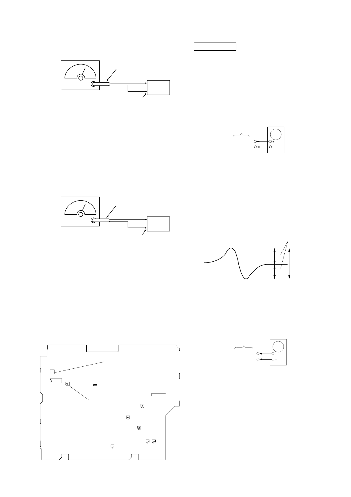
S-Curve Check
Oscilloscope
BD board
TP(FE)
TP(DVC)
Procedure :
1. Connect oscilloscope to TP (FEO).
2. Connect between TP (FE) and TP (DVC) by lead wire.
3. Turn Power switch on.
4. Load a disc (YEDS-18) and actuate the focus search. (In
consequence of open and close the disc tray, actuate the focus
search)
5. Confirm that the oscilloscope waveform (S-curve) is
symmetrical between A and B. And confirm peak to peak level
within 4 ±1 Vp-p.
S-curve waveform
symmetry
A
±
within 4
B
7. After check, remove the lead wire connected in step 2.
Note : • Try to measure several times to make sure than the ratio
of A : B or B : A is more than 10 : 7.
• Take sweep time as long as possible and light up the
brightness to obtain best waveform.
RF Level Check
1Vp-p
T11
12
13
1
IC11
RV11
24
FM TUNED LEVEL
CN301
NULL
RV351
RV301
RV303
RV304
RV302
RV354
CN304
Procedure :
1. Connect oscilloscope to TP (RFAC).
2. Turned Power switch on.
3. Load a disc (YEDS-18) and playback.
4. Confirm that oscilloscope waveform is clear and check RF signal
level is correct or not.
5. Measure the RFDC in the same way.
19
HCD-VP800AV
)
Note: Clear RF signal waveform means that the shape “◊” can be
clearly distinguished at the center of the waveform.
RF signal waveform
VOLT/DIV : 200mV
TIME/DIV : 500ns
level : 1.1 ± 0.3Vp-p
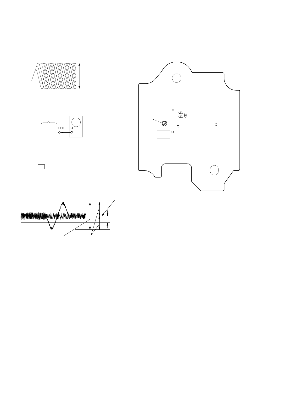
E-F Balance (1 Track jump) Adjustment
oscilloscope
BD board
TP (TE)
TP (DVC)
+
–
Procedure:
1. Connect oscilloscope to TP (TE) and TP (DVC) board.
2. Turned Power switch on.
3. Load a disc (YEDS-18) and playback the number five track.
4. Press the X button. (Becomes the 1track jump mode.)
5. Confirm that the level B and A (DC voltage) on the oscilloscope
waveform.
Adjustment Location :
[ BD (CD) BOARD ] — SIDE B —
TP (DVC)
RV101
IC103
TP(TE)
TP(RFDC)
TP
(RFAC)
TP(SE)
TP(FE)
IC101
TP
(XPCK)
1 track jump waveform
Center of
waveform
B
0V
level=1.3 ±0.6Vp-p
Symmetry
A (DC voltage
Specification level: x 100=less than ±22%
6. Adjust RV101 so that (DC voltage) becomes 0.
7. After check, remove the lead wire connected in step 1.
20
VIDEO SECTION
r
Frequency Adjustment
Connection:
frequency counte
VIDEO board
(27 MHz)
Procedure:
1. Connect the frequency counter to check point of the VIDEO
board.
2. Turned power switch on.
3. Press the CD button to select the CD.
4. Adjust CT503 on the VIDEO board so that the frequency counter
reading 27.0 MHz ± 80 Hz at stop status.
Adjustment Location:
[VIDEO BOARD] (SIDE A)
HCD-VP800AV
CN501
J301
CN502
J302
(27MHz)
IC507
(GND)
CT503
VIDEO
Frequency
Adjustment
CN503
21
HCD-VP800AV
SECTION 6
DIAGRAMS
THIS NOTE IS COMMON FOR PRINTED WIRING BOARDS AND SCHEMATIC DIAGRAMS.
(In addition to this, the necessary note is printed in each block.)
Note on Schematic Diagram:
• All capacitors are in µF unless otherwise noted. pF: µµF
50 WV or less are not indicated except for electrolytics
and tantalums.
• All resistors are in Ω and 1/
specified.
f
•
• C : panel designation.
• A : B+ Line.
• B : B– Line.
• H : adjustment for repair.
• Voltages and waveforms are dc with respect to ground
• Voltages are taken with a VOM (Input impedance 10 MΩ).
• Waveforms are taken with a oscilloscope.
• Circled numbers refer to waveforms.
• Signal path.
• Abbreviation
: internal component.
Note:
The components identified by mark 0 or dotted
line with mark 0 are critical for safety.
Replace only with part
number specified.
under no-signal (detuned) conditions.
Voltage variations may be noted due to normal production tolerances.
Voltage variations may be noted due to normal production tolerances.
F : FM
f : AM
E : PB (DECK A)
d : PB (DECK B)
G : REC (DECK B)
J : CD
c : digital out
g : MD (VIDEO)
SP : Singapare model
MY : Malaysia model
TH : Thai model
JE : Tourist model
4
W or less unless otherwise
Note on Printed Wiring Boards:
• X : parts extracted from the component side.
• : Pattern from the side which enables seeing.
• Indication of transistor.
These are omitted.
Q
B
CE
These are omitted.
C
Q
B
E
22
HCD-VP800AV
1 IC101 t; (RFAC)
CD PLAY MODE
1.2Vp-p
2 IC101 ra (TE)
CD PLAY MODE
3 IC101 el (FE)
CD PLAY MODE
400nsec/div
approx 400mVp-p
approx 170mVp-p
1
IC1101 is (XOUT)
STOP MODE
3Vp-p
4MHz
d
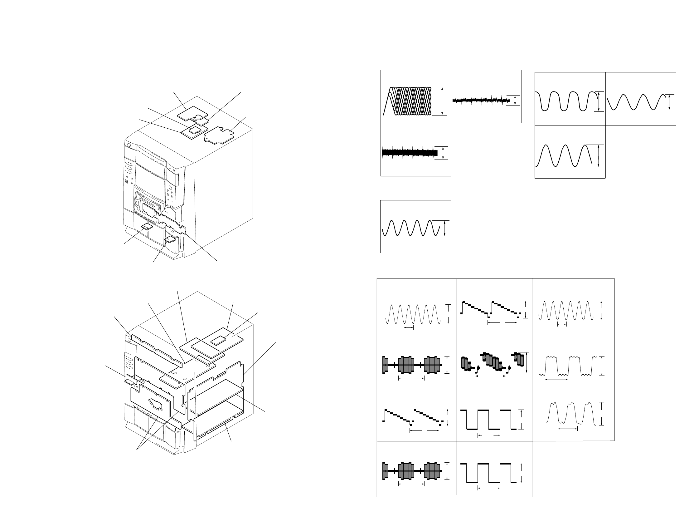
6-1. CIRCUIT BOARD LOCATION
CD SENSOR board
VIDEO board
MOTOR board
DRIVER board
BD board
• WAVEFORMS
– BD BOARD –– MAIN BOARD –
1 IC401 qa (XC-OUT)
STOP MODE
32.768kHz
2 IC401 qd (X-OUT)
STOP MODE
16MHz
– PANEL BOARD –
3 T301 4
TAPE B REC MODE
3.0Vp-p
2.8Vp-p
80.1kHz
130Vp-p
HEAD (A) board
CD PANEL board
OPT IN board
HEAD (B) board
TRANS board
SUB TRANS board
LEAF SW board
DSP board
OPT IN REAR board
MAIN board
SURROUND AMP boar
– VIDEO BOARD –
1
IC502 qd (XOUT)
10MHz
2
IC505 ug (C-OUT)
H
3
IC505 yl (Y-OUT)
9
5
IC304 qg (Y-OUT1)
4.6Vp-p
6
IC304 qs (MIX OUT1)
0.5Vp-p
7
IC509 ql (LRCK)
1.0Vp-p
H
22.7
H
µ
s
2.0Vp-p
H
1.3 Vp-p
4.5Vp-p
IC509 wf (XT2)
37ns
q;
IC504 8
59ns
qa
IC504 6
37ns
2.0Vp-p
4.8Vp-p
4.8Vp-p
PANEL board
FRONT AMP board
4
IC304 9 (C-OUT)
H
2323
2.0Vp-p
8
IC509 qj (BCK)
4.5Vp-p
472ns
HCD-VP800AV
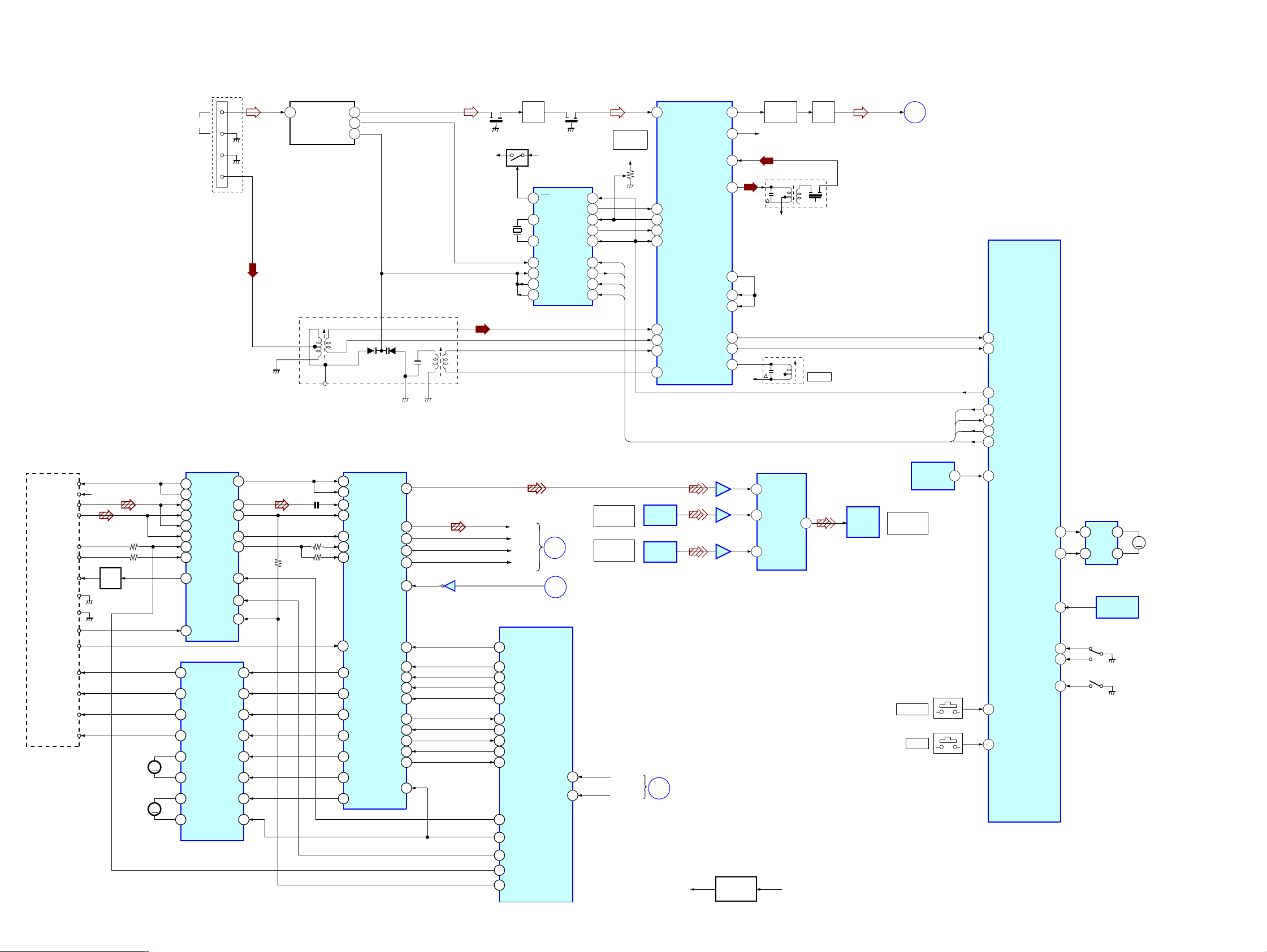
6-2. BLOCK DIAGRAMS
– TUNER/CD SECTION –
OPTICAL PICK-UP
BLOCK
(A-MAX.3)
VC
+5V
VCC
PD1
PD2
I5-10
I1-6
LD
LD GND
GND
PD
SW
F+
T+
Q101
LD
DRIVE
F-
T-
M102
SLED
MOTOR
M101
SPINDLE
MOTOR
IC102
M
M
TM1
FM 75Ω
G
AM
IC103
RF AMP
27
VC
25
VFC
6
A
7
B
8
C
9
D
10
E
11
F
1
LD
RFDCI
2
PD
MOTOR/COIL DRIVE
52
VO1(-)
47
VO1(+)
56
VO2(-)
55
VO2(+)
1
VO3(+)
2
VO3(-)
5
VO4(+)
10
VO4(-)
1
ANT IN
2
11
14
DVC
RFAC
15
RFDC
28
16FE
18TE
SW
12
FEI
17
29
IN1+
35
IN1-
34
IN2+
32
31
IN2-
27
IN3+
IN3-
26
IN4R
24 MDP
STBY
8
FE1
IF OUT
7
OSC OUT
8
VT
5
10
49
RB41
IC101
DIGITAL SERVO
DIGITAL SIGNAL PROC.
38
VC
CE
RFAC
RFDC
FE
TE
SE
D OUT
PCMD
BCLK
LRCK
C2PO
XTAI
42
50
43
39
41
40
6
64
66
67
65
14
71
1
3
8
7
4
2
IC106
26 SSTP
33
FFDR
34
FRDR
31
TFDR
32
TRDR
29
SFDR
30
SRDR
25
XTSL
DATA
CLOK
XLAT
MUTING
SQSO
SQCK
SENS
SCLK
SCOR
XRST
CTRL1(1-2)
69
4
6
5
3
76
77
7
8
15
2
DATA
CLK
XLT
MUTING
SQSO
SQCK
SENS
SCLK
SCOR
LDON
XRST
PWM1
PWM2
PWM3
Q2
ADATA
BCLK
LRCK
C2PO
IC502(1/2)
11
CTRL1
95
DSP DATA
5
DSP CLK
97
DSP LATCH
10
DSP MUTING
84
SUBQ DATA
83
SUBQ CLK
1
SENSE
2
SENSE CLK
18
SCOR
82
LD ON
77
DEVICE RESET
28
PWM1 (BD)
26
PWM2 (BD)
24
PWM3 (BD)
Q1
RF IF
AMP
10
1
22
16
20
19
18
MCLK
CF1 CF2
+B
(FE1-3)
X51
4.5MHz
CD DATA
CD BCK
CD LRCK
CD MECHANISM CONTROLLER
FM TUNED
A+12V
PLL
LEVEL
A+12V
IC51
IF IN
FM
XIN
XOUT
FM OSC
AOUT
AIN
PD
VIDEO
SECTION
(Page 26)
D
C
I2C.DATA I2C-DATA
I2C.CLK I2C-CLK
FM
AM OSC
CL
CE
VIDEO
SECTION
(Page 26)
30
29
12
7
15
9VCO STOP
8IF REQ
6DO
4DI
5
3
DIGITAL IN
OPTICAL
DIGITAL IN
OPTICAL
DO
DI
DI
CL
CE
RV11
IC1195
DIGITAL
IC801
DIGITAL
1
FM IF
11
AM/FM
24
OSC FM
12
VCO STOP
10
IF REQ MUTE
21
AM RF IN
22
AFC
23
AM OSC
VCC
9
IN
IN
E
AM/FM IF MPX
IC11
AM IF IN
AM MIX OUT
DECORDER
PLL IN OUT
DECORDER
MAIN
SECTION
(Page 25)
+3.3V
L OUT
R OUT
IN
TUNED
STEREO
FM-DET
IC608
3
5
IC608
1
IC608
13
14
4
2
18
17
16
6
7
8
A+12V
10
8
12
Q103,D101
+3.3V
REG.
BUFFER
Q11
R-CH
A+12V
AEP
DIGITAL AUDIO
INTERFACE
IC604(2/2)
DIN0
3
DIN1
4
SPDIF
5
DIN2
+5V
IFT11
2
T11
LPF11
NULL
LPF
IC609
OPTICAL
DIGITAL
OUT
OUT
L-CH
(Page 25)
DIGITAL OUT
OPTICAL
A
MAIN
SECTION
DISPLAY
_/1
IC1102
REMOTE
SENSOR
S1135
S1115
• RCH is omitted
• Signal Path
: FM
F
: AM
f
: CD
J
: DIGITAL OUT
c
MASTER CONTROL
IC401(1/2)
TUNED
88
STEREO
87
21
ST MUTE
DO
23
25
27
22
4
ST-DOUT
ST-DIN
ST-CLK
CE
SIRCS
DI
CL
CE
1
IC701
LOAD IN
9
44
45LOAD OUT
7
MOTOR
DRIVE
4
2
M721
M
TURN
MOTOR
IC711
TBL ADDRESS
SENSOR
OPEN/CLOSE
S711
BU UP/
DOWN
S701
BU UP/DOWN SW
73
DISPLAY KEY
74
POWER KEY
T SENS
49
46OPEN SW
47CLOSE SW
48
2424
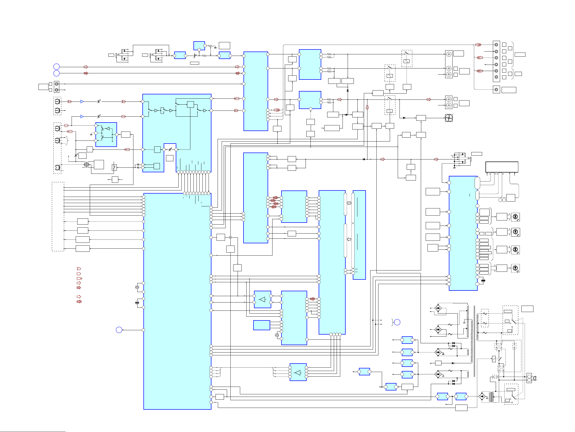
– MAIN SECTION –
TUNER/CD
SECTION
(Page 24)
VIDEO
SECTION
(Page 26)
MD/VIDEO
(AUDIO)
HEAD
REC/PB
HEAD
ERASE
HEAD
L
R
PB
A
B
J101
DECK-A
DECK-B
TC BLOCK
A120/70
B120/70
B SHUT
A SHUT
B PLAY
A PLAY
B HALF
A HALF
A TRG M+
B TRG M+
CAP M H/L
CAP M+
CN304
L-CH
L-CH
L-CH
R-CH
IC303
R-CH
R-CH
R-CH
E+6V
g
g
PB EQ
AMP
PB EQ
AMP
IC304
RV304
REC
BIAS(L)
E+6V
Q393,394
A TRIG
DRIVE
Q391,392
B TRIG
DRIVE
Q395
CAP MOTOR
SPEED CONT
Q396,397
CAP MOTOR
DRIVE
• RCH is omitted
• Signal Path
C332,L301
BIAS
TRAP
T301
: PB (DECK A)
: PB (DECK B)
: REC (DECK B)
: FM
: CD
: MD(VIDEO)
: AM
: DIGITAL OUT
RV302
RV303
REC/PB SWITCH
IC302
1
2
3
BIAS
OSC
Q302,303
+6V
VIDEO
SECTION
(Page 26)
Q301
J1201
MIC1
R CH
TC A+12V
Q141
BIAS
HCD-VP800AV
IC1220
ECHO
9
AMP
2
1
RV1201
MIC-VOL
DOLBY
B
DOL
PAS
BIAS ON/OFF
B NORM/CROM/METAL
ALC ON/OFF15RM ON/OFF22NR ON/OFF23REC /PB/PASS24LM ON/OFF25MS OUT
PB A/B16NORM/HIGH
20
18
67
66
68
65
61
60
ALC
BIAS
PB A/B
EQ H/N
REC MUTE
SP PROTECT
FRONT RELAY
REAR RELAY
CODEC-SMUTE
DSP-DECODE
DIR-UNLOCK
CD/DVDPOWER
STBY RELAY
59
58
R/PB PAS
NR ON/OFF
AMP-DATA
AMP-CLK
AMP-LAT
STK-MUTE
LINE-MUTE
DSP-CS
DIG-TX
DIG-CLK
DIR-STATE
DIR-RX
DIR-CS
IICDATA
IICCLK
M-RESET
DSP-RX
DSP-ACK
ACOUT
RESET
REC
70
120
38
RV301
REC(L)
LEVEL
IC1201(1/2)
MIC
3
AMP
DECK PROC.
IC301
REC
PB
39
A120/70
17
19
MASTER CONTROL
IC401(2/2)
J1202
MIC2
48
A
B
46
SWITCH
4
Q304,305
EQ OUT(L)
REC
36
EQ
NORM
33
BIAS
CROM
SW
32
DC
TC A+12V
B SHUT
90
A SHUT
89
57
B PLAY
A PLAY
56
B HALF
91
70
A HALF
TC RELAY
69
A TRIG
50
B TRIG
52
CAP M H/L
54
55
CAP M CONT
XC IN
10
X401
32.768kHz
X402
16MHz
F
XC OUT
11
X OUT
13
X IN
15
X RST
43
PB
26
53
TC MUTE
FAN
43
40
AMS IN
86
84
1
2
3
85
72
71
79
81
5
7
77
78
76
94
30
29
41
6
80
82
15
98
100
12
83
RV1202
ECHO
LEVEV
MIC
7
6
AMP
IC1201(2/2)
Q502
LINE
MUTE
Q504-506
POWER
MUTE
Q501
RESET
SWITCH
MUTE
SWITCH
Q612
1
67
71
69
64
70
15
16
17
IC607(1/2)
SOUND PROCESSOR
MAC IN
LIN2
SLOUT
LIN6
LIN4
LREC OUT1
FLOUT
LREC OUT
LIN5
SWOUT
FRBB2
FRBB1
FLBB2
FLBB1
IC607(2/2)
SOUND PROCESSOR
ADL+OUT
ADL-OUT
L-REC IN
B PLAY
PORT3
B PLAY
B PLAY
PORT1
PORT4
PORT5
IC603(2/2)
BUFFER
6
2
IC604(1/2)
DIGITAL IN
REFER TO
IC604(2/2)
IC1001
COUT
32
36
Q610
15
MUTE
14
Q609
MUTE
IC801
46 10
63
66
LIN1
69
LIN4
28
Q611
MUTE
52
51
45
44
MULTI-CHANEL AUDIO DECODE
6
30
7
9
2
20
18
21
22
X601
13.5MHz
5
1
29
27
25
17
3
17
35
37
36
38
3
4
5
21
22
DSP-RX
DSP-DATA
DSP-DECODE
DIR-UNLOCK
FLIN
Q607
MUTE
Q604
DBFB
CONT
Q605
DBFB
CONT
IC605
LIN+
LINLOUT1
LOUT2
PDN
SMUTE
Q613
RESET
SWITCH
IC604(1/2)
DIGITALAUDIO
INTERFACE
XSTATE
DO
CE
DI
CL
DIN0
DIN1
DIN2
XOUT
XIN
IC603(1/2)
BUFFER
12
10
8
4
18
MCLK
DATA0
DATA1
DATA2
DATA3
LRCK
DATA
LRCK
CKOUT
XMCK
AUDIO
ERROR
Q821,822
BCK
BCK
Q823
13
11
POWER
AMP
POWER
AMP
MUTE
MUTE
SWITCH
39
4
9
6
7
8
5
16
14
15
13
20
24
34
9
3
R-CH
SW
KEY
KEY
KEY
D1071
D950
D959
D871
Q971
REG
IC501
3
RESET
EVER5.7V
AC1
AC1
AC2
AC2
AC3
AC3
AC4
AC4
TM1001
TM801
M961
FAN
R CH
58
64
64
65
66
56
57
60
61
77
F916
F917
F918
F919
1
D830,831
D961,962
CENTER
SPEAKR
L
SPEAKR
R
L
SPEAKER
R
DISPLAY CONTROL
IC1101
HEADPHONE
KEY0
KEY0
PB7/SO1 LED11
PA3/AN3 LED10
KEY1
RLED5 FIP/LED0
KEY2
VOL 1A
VOL 1B
PB1/C11 LED14
IIC DATA
IICCLOCK
RSTX
D911
IC901
+5.7V
3
REG
RELAY
DRIVER
Q901
REAR
FRONT
J1101
PHONES
2-10
FIP17
12-22
I
24-41
FIP59
43-47
FIP/LED5
100
FIP/LED16
PLAY1
PB4/AN2 LED9
LED4 FIP/LED1
PB6/AN13
PB6/AN14
PB7/AN15
LED1 FIP/LED2
LED1 FIP/LED3
PB0/IC1 LED15
XIN
XOUT
T911
POWER TRANSFORMER
1
R-CH
R-CH
90
I
55
59
67
76
85
86
78
79
80
87
88
89LED1 FIP/LED4
52
53
54PB8/S10 LED13
83
82
RY1082
18
17
RY1081
7
6
Q1051
OVERLOAD
DETECTOR
11
12
+B
14
20
18
23
20
25
19
67
56
2
113
36
33
34
30
29
28
22
12
9
69
OVER LOAD
Q816,817
TEMPERATURE
DETECTOR
AUDIO DECODER
SCKOUT
BCK
SDI1
SDO1
SDO4
SDO3
LRCKO
GP10
BST
XRST
PM
HCS
HD IN
HCLK
SDI2
BCKI2
LRCKI2
KFSI2
MCLK2
MCLK1
GP8(AUDIO)
DETECTOR
IC601
HACN
323568
RY881
Q801
HDOUT
GP9(DECODE)
Q1041
OVERLOAD
DETECTOR
D1091
Q835-837
D891
Q831,832
FEED BACK
72
I
80
•
98
•
99
•
102
I
108
64
I
66
•
83
I
85
•
92
I
97
•
109
•
110
•
112
CSO
45
WEO
EXLOCK(ERROR)
59
PROTECT
DETECTOR
PROTECT
CONT
IC602
16
D15
I
13
•
10
I
7
•
38
I
35
•
32
D0
I
29
20
I
18
•
A15
2
I
4
•
1
•
5
•
21
•
24
A0
•
42
I
44
•
27
I
25
61744
CS
WE
S-RAM
D606
Q1084
INVERTER
Q833,834
PROTECT
I2C-DATA
I2C-CLK
TC+9V
RY881
RELAY
DRIVE
RELAY
DRIVE
Q881,882
RELAY
DRIVE
D111
Q507
MUTE
TUNER/CD
SECTION
E
(Page 24)
IC922
3
REG
MUTE
MUTE
SWITCHT
Q121
Q503
1
Q111-113
FAN
DRIVER
Q114
FAN
SWITCH
S1136-1138,1140-1148
S1110-1114
S1129-1134,1139
S1116-1128
+VH
-VH
+VL
-VL
R-CH
S1135
DISPLAY
FUCTION
FUCTION
FUCTION
S1101
VOLUME
IC923
A+12V
IC610
3
2.6V
1
REG
SWD+5V
D+3.3V
3
D+5V
IC931
5VREG
3
1
REG
IC932
3
(UNREG+16V)
1
REG
VP
(-30V)
IC934
3
1
REG
(UNREG+9V)
Q931,932
B+SWITCH
1
L REC OUT
SWOUT
F1
MULTI
CHANNEL
DECODING
EFFECT
GROOVE
LED CTL
ENTER
REC /
GAME
DIGITAL
MD(VIDEO)
TAPE A/B
TUNER/BAND
TUNER
CD
DISC1
DISC2
DISC3
4.0MHz
MY, SP, JE
F911
F912
F913
MY, SP, JE
JW905
TH
D902-905
TRANSFORMER
L IN1
L IN4
X1101
JW906
RY901
JW901
MY, SP, JE
T901
SUB
J601
L
R
L
R
L
R
J602
SUB WOOFER
FL1101
FLOURESCENT
INDICATOR TUBE
Q1123,1124
97 99
Q1107,1111
1112
LED
DRIVER
Q1108-1110,
1113
LED
DRIVER
Q1101-1106
LED
DRIVER
Q1114-1116
LED
DRIVER
MY, SP, JE
S901(1/2)
230-240
220
TH
JW907
MY, SP, JE
S901(2/2)
120
OUT
IN
IN
OUT
GRID
DRIVER
D1107,1111
D1108,1113
D1101-1106
D1114-1116
120
JW902
230-240
F2
1112
JW903
MD VIDEO
GAME
S901
VOLTAGE
SELECTOR
CN901
2
AC
IN
1
2525
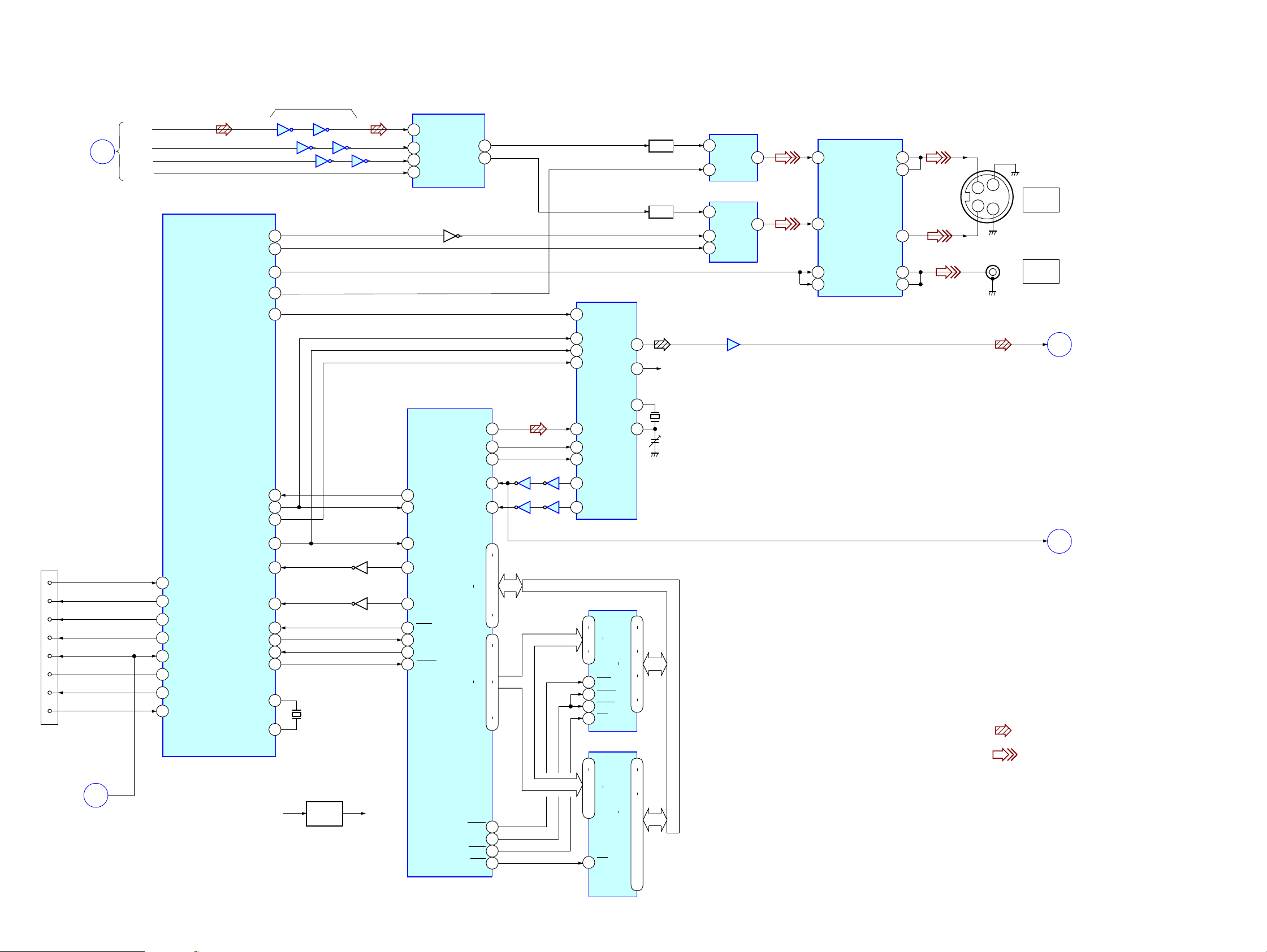
HCD-VP800AV
– VIDEO SECTION –
TUNER/CD
SECTION
(Page 24)
CN503
(TO FLASH WRITER)
TXD
SCLK
BUSY
RXD
RST
PGM
XWR
HOLD
MAIN
SECTION
(Page 25)
IC501
BUFFER
324
13
5
1112 10
968
D
ADATA
BCLK
LRCK
C2PO
BGP
CROMA LEVEL
DAC RESET
1
22
4
65V.MUTING
3RESOLUTION
66
IC502(2/2)
CD MECHANISM
CONTROLLER
DATAI
36
DATAO
35
CLK1
XIN
XOUT
88
37
21H SYNC IN
45V SYNC
20
87
85
86
15
13
+5V
X501
10MHz
Q531
+3.3V REG
Q501
Q502
+3.3V
(IC505 VDD)
DF LATCH
DATA1I
32
CLK1
33
RTS1
34
DATA1O
31
XRESET
12
CNVSS
9
BUS XWRL
46
BUS XHOLD
41
XRST
F
CL680 INTERRUPT
CL680 HSEL
CL680 HRDY
680 RESET
IC505 (1/2)
MPEG VIDEO/AUDIO DEC
VIDEO SIGNAL PROC
4
CD-DATA
3
5
6
CD-BCK
CD-LRCK
CD-C2PO
Y OUT
C OUT
Q301
IC505 (2/2)
MPEG VIDEO/AUDIO DEC
VIDEO SIGNAL PROC
DA DATA
DA BCK
DA LRCK
DA XCLK
112
HD OUT
119
HD IN
117
HCK
101
H SYNC
93
V SYNC
114
HINT
121
HSEL
113
HRDY
60
RESET
VCK IN
MD0
MD15
MA0
MA10
RAS0
CAS
MWE
MCE
IC303
Y AMP
69
75
IC509
DIGITAL FILTER
D/A CONV
10
RSTB
9
MD
V OUT L
8
MC
7
ML
V OUT R
XT1
110
111
108
106
IC504
86
IC504
27MHz
10
15
.
17
.
19
.
21
.
23
29
58
56
.
54
.
52
50
.
48
.
46
44
42
40
38
37
18
17
19
111098
20
3456
4
DATA
BCK
LRCK
384FSO
MCKO
IC507
DRAM
16
A0
19
.
A8
22
26
14
RAS
28
UCAS
29
LCAS
13
WE
IC510
FLASH ROM
12
5
.
A0
27
.
A10
26
.
23
CE
22
DQ1
DQ16
O0
O7
A11
A17
XT2
ı
L.P.F
L.P.F
14
11
R-CH
1
X503
27MHz
24
2
5
.
7
10
.
31
34
.
36
39
13
15
.
17
21
.
25
.
4
.
28
.
29
.
3
.
2
.
30
10
VIN
5
CCT
IC302
1
VIN
5
BGP
8
TINT
IC101
C AMP
VOUT
L.P.F
1VOUT
6
75
IC304
VIDEO MIX BUFFER
2
Y IN
7
C IN
1
MUTE A
8
MUTE B
C OUT
15Y OUT1
14Y OUT2
9
12MIX OUT1
11MIX OUT2
Y
2
4
3
1
C
V
J301
S VIDEO
OUT
J302
VIDEO
OUT
LOUT
MCLK
• R-ch is omitted due to same as L-ch.
• Signal Path
: CD
: VIDEO
MAIN
SECTION
B
(Page 25)
CD
SECTION
C
(Page 24)
2626
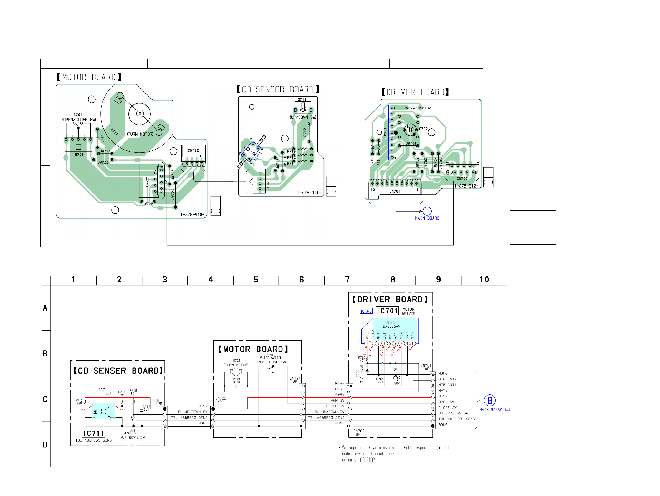
6-3. PRINTED WIRING BOARD – DRIVER SECTION – • See page 23 for Circuit Boards Location.
HCD-VP800AV
A
B
C
D
12
3456 7 89
14
14
14
14
14
B
(Page 30)
14
• Semiconductor
Location
Ref. No. Location
D701 B-7
IC701 B-8
IC711 B-5
6-4. SCHEMATIC DIAGRAM – DRIVER SECTION – • See page 61 for IC Block Diagrams.
(Page 31)
2727
 Loading...