

Page 1
HCD-V8800
SERVICE MANUAL
HCD-V8800 is the tuner, deck, Video CD and
amplifier section in LBT-V8800AV.
Model Name Using Similar Mechanism HCD-V4500
CD
SECTION
TAPE
DECK
SECTION
CD Mechanism Type CDM37L-5BD21AL
Base Unit Type BU-5BD21AL
Optical Pick-up Type KSS-213D/Q-NP
Model Name Using Similar Mechanism HCD-V4500
Tape Transport Mechanism Type TCM-220WR2
E Model
Chinese Model
SPECIFICATIONS
— Continued on next page —
MICROFILM
COMPACT DISC DECK RECEIVER
— 1 —
Page 2
CAUTION
Use of controls or adjustments or performance of procedures
other than those specified herein may result in hazardous radiation exposure.
Notes on chip component replacement
• Never reuse a disconnected chip component.
• Notice that the minus side of a tantalum capacitor may be
damaged by heat.
Flexible Circuit Board Repairing
• Keep the temperature of soldering iron around 270˚C
during repairing.
• Do not touch the soldering iron on the same conductor of the
circuit board (within 3 times).
• Be careful not to apply force on the conductor when soldering
or unsoldering.
Laser component in this product is capable of emitting radiation
exceeding the limit for Class 1.
This appliance is classified as
a CLASS 1 LASER product.
The CLASS 1 LASER PRODUCT MARKING is located on
the rear exterior.
This caution
label is located
inside the unit.
MODEL IDENTIFICATION
— BACK PANEL —
MODEL
E, SP model
MY model
CH model
IA model
SAFETY-RELATED COMPONENT WARNING !!
COMPONENTS IDENTIFIED BY MARK ! OR DO TTED LINE
WITH MARK ! ON THE SCHEMATIC DIAGRAMS AND IN
THE PARTS LIST ARE CRITICAL TO SAFE OPERATION.
REPLACE THESE COMPONENTS WITH SONY PARTS
WHOSE PART NUMBERS APPEAR AS SHOWN IN THIS
MANUAL OR IN SUPPLEMENTS PUBLISHED BY SONY.
PARTS No.
4-992-220-0
4-992-220-1
4-992-220-2
4-992-220-3
• Abbreviation
SP : Singapore model
MY : Malaysia model
IA : Indonesian model
CH : Chinese model
— 2 —
Page 3

NOTES ON HANDLING THE OPTICAL PICK-UP BLOCK
OR BASE UNIT
The laser diode in the optical pick-up block may suffer electrostatic
break-down because of the potential difference generated by the
charged electrostatic load, etc. on clothing and the human body.
During repair, pay attention to electrostatic break-down and also
use the procedure in the printed matter which is included in the
repain parts.
The flexible board is easily damaged and should be handled with
care.
NOTES ON LASER DIODE EMISSION CHECK
The laser beam on this model is concentrated so as to be focused on
the disc reflective surface by the objective lens in the optical pickup block. Therefore, when checking the laser diode emission, observe from more than 30 cm away from the objective lens.
LASER DIODE AND FOCUS SEARCH OPERATION
CHECK
Carry out the “S curve check” in “CD section adjustment” and check
that the S curve waveform is output three times.
TABLE OF CONTENTS
1. SERVICING NOTE
.......................................................... 4
2. GENERAL .......................................................................... 6
3. DISASSEMBLY
3-1. Front Panel ........................................................................... 7
3-2. Main Board ........................................................................... 8
3-3. Tape Mechanism Deck .......................................................... 8
3-4. Cassette Lid Assembly..........................................................9
3-5. CD Lid Assembly.................................................................. 9
3-6. CD Mechanism Deck .......................................................... 10
3-7. Base Unit ........................................................................... 10
3-8. Disc Table ........................................................................... 10
4. TEST MODE ..............................................................11
5. MECHANICAL ADJUSTMENTS ...........................12
6. ELECTRICAL ADJUSTMENTS ............................... 12
7. DIAGRAMS
7-1. Circuit Boards Location ...................................................... 17
7-2. Block Diagrams
• KEY CON Section........................................................... 18
• CD Section ....................................................................... 19
• Video Section................................................................... 21
• Deck Section .................................................................... 23
• Main Section .................................................................... 25
• Power Section .................................................................. 27
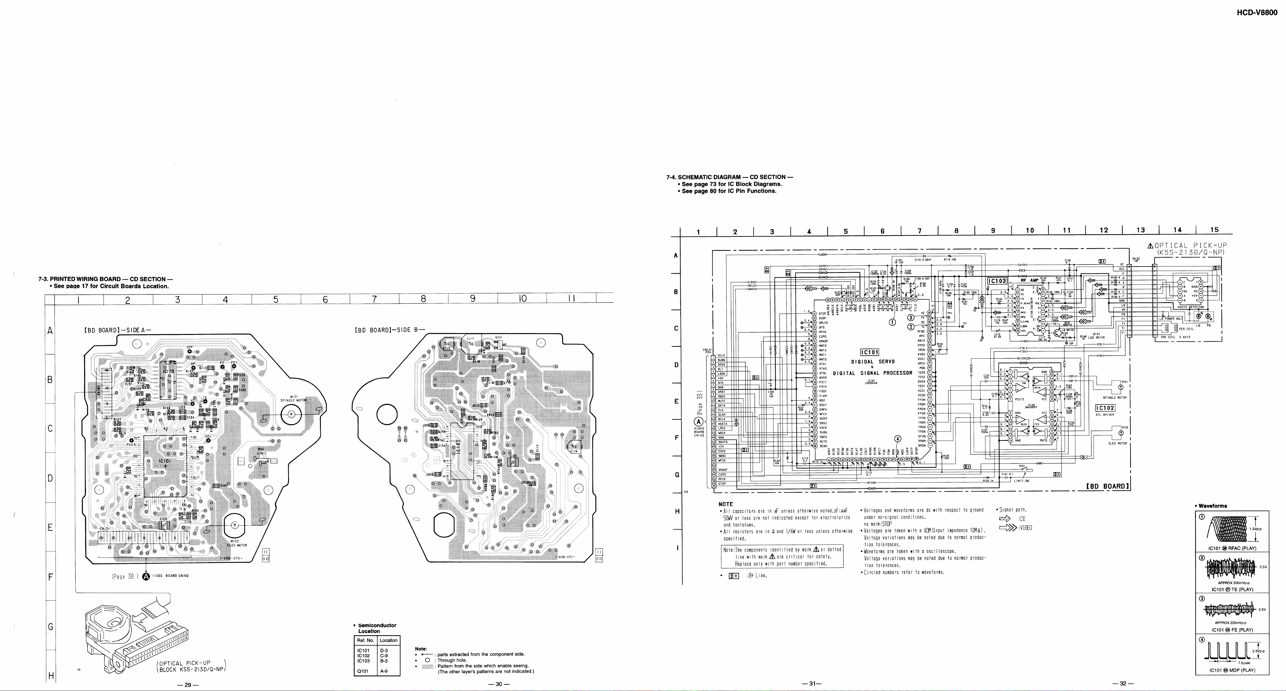
7-3. Printed Wiring Board — CD Section —............................. 29
7-4. Schematic Diagram — CD Section — ............................... 31
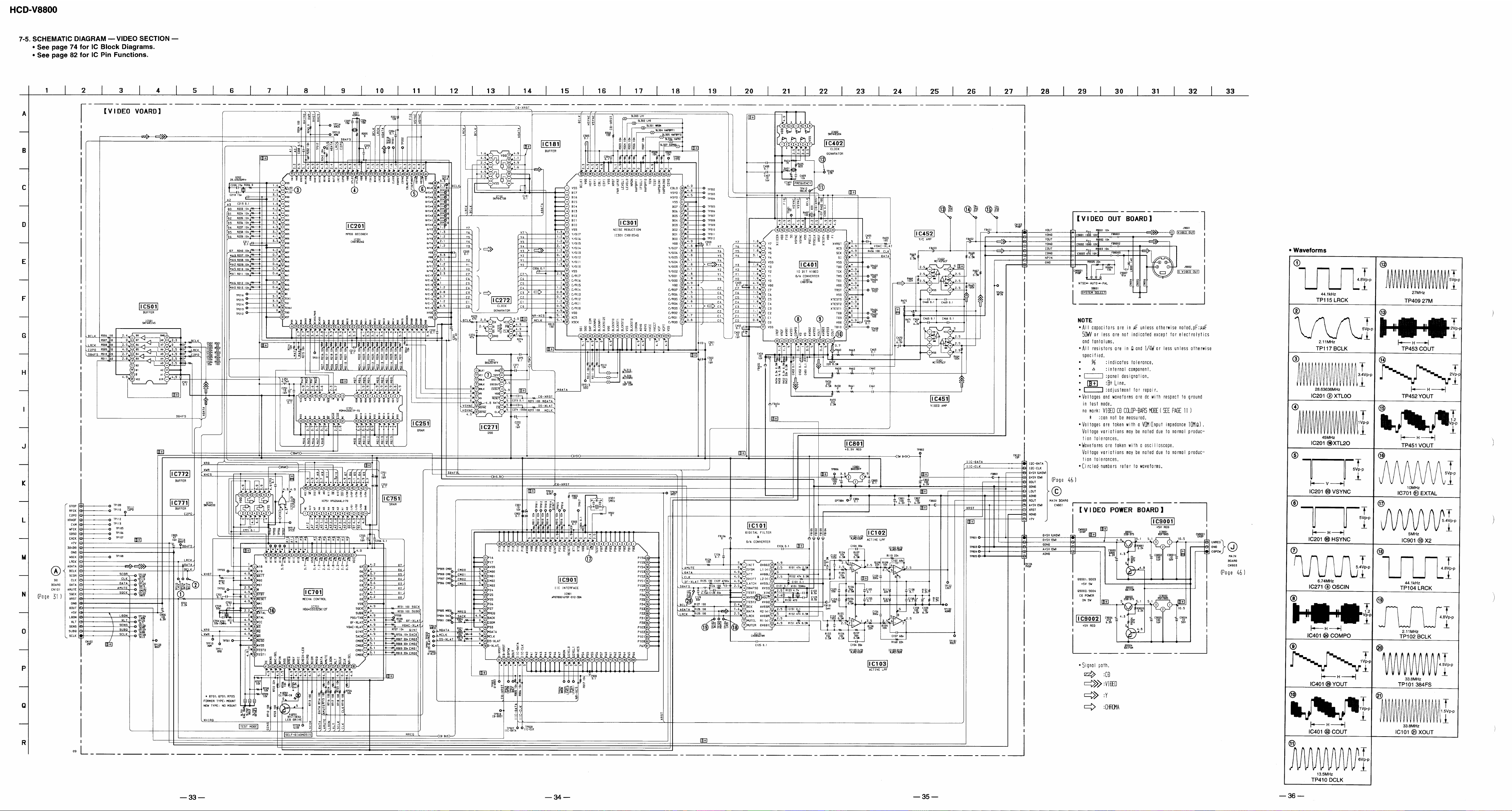
7-5. Schematic Diagram — Video Section — ........................... 33
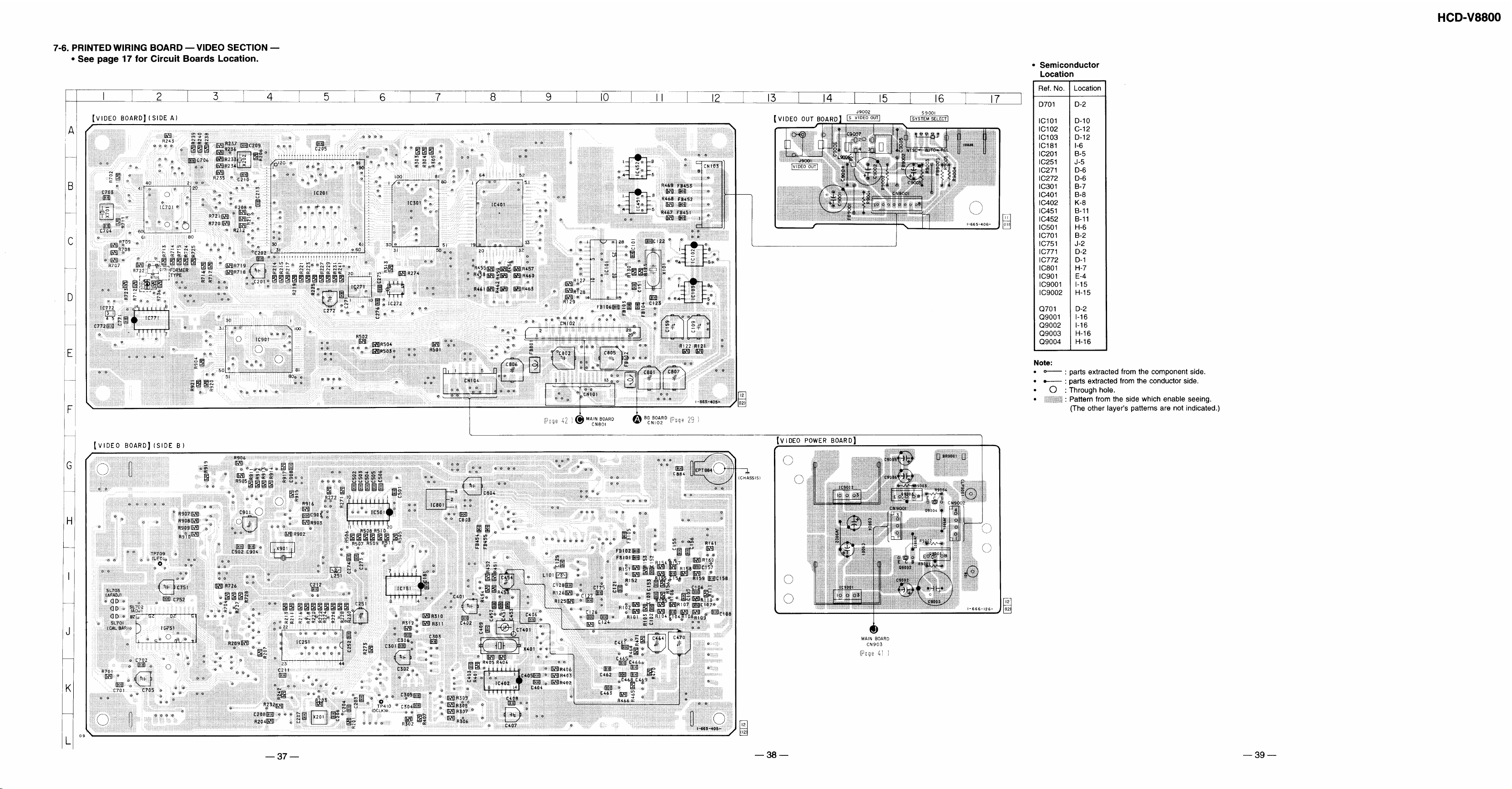
7-6. Printed Wiring Board — Video Section —......................... 37
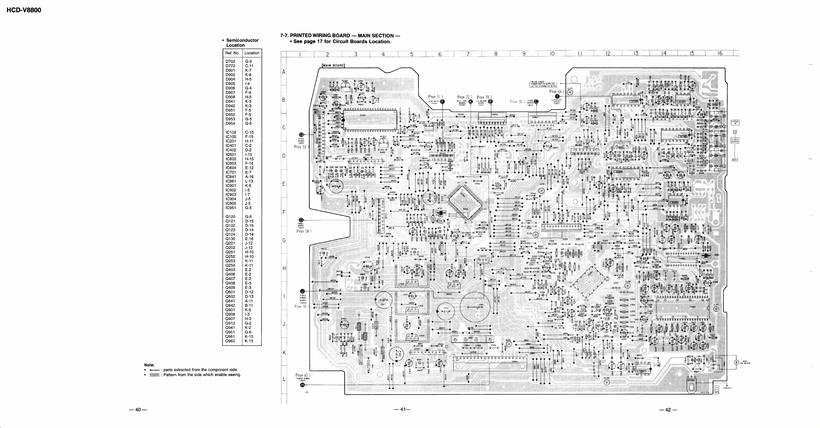
7-7. Printed Wiring Board — Main Section —.......................... 40
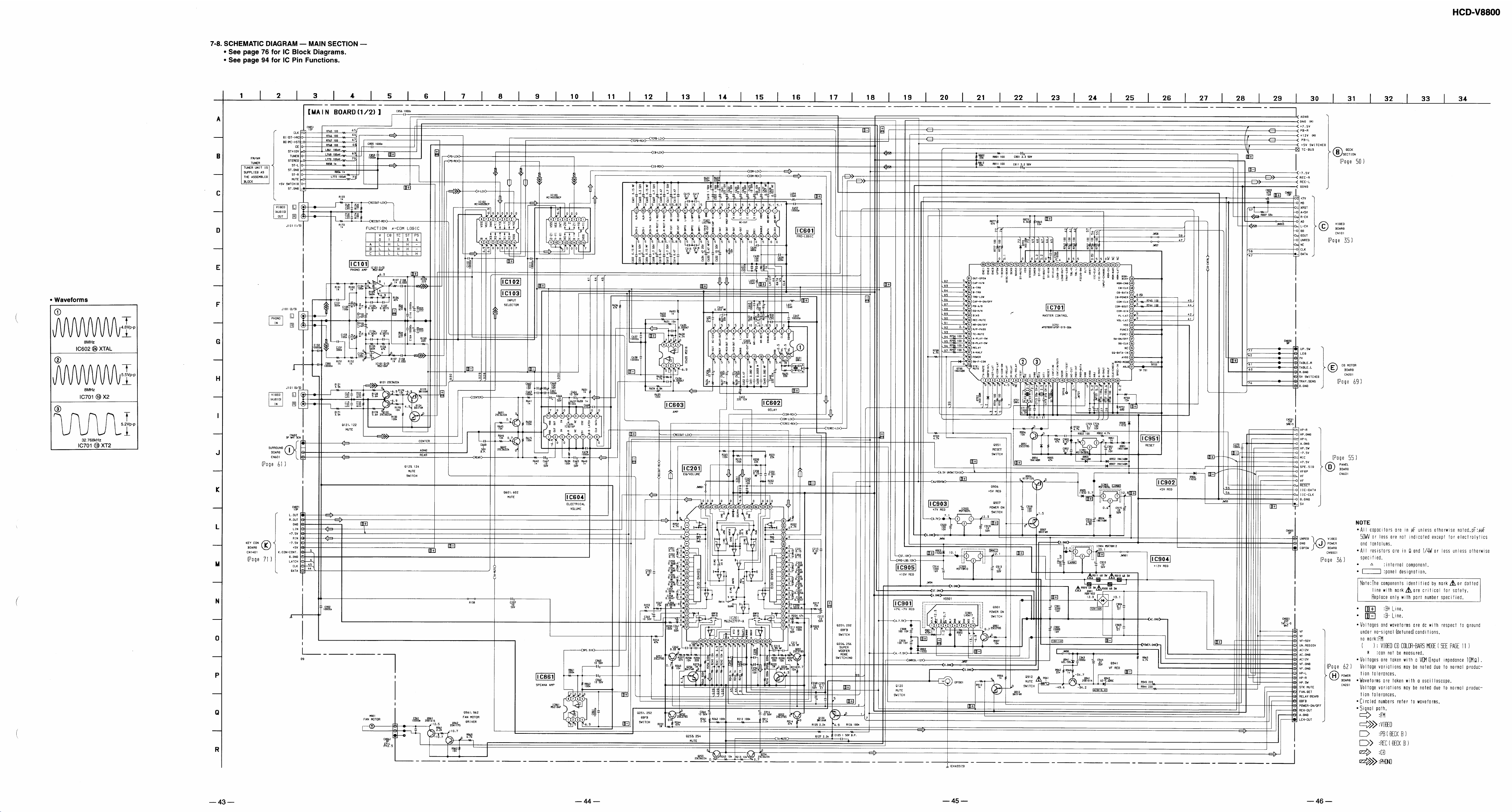
7-8. Schematic Diagram — Main Section — ............................ 43
7-9. Schematic Diagram — Deck Section — ............................ 47
7-10. Printed Wiring Board — Deck Section — ....................... 51
7-11. Schematic Diagram — Panel Section — .........................54
7-12. Printed Wiring Board — Panel Section —....................... 57
7-13. Schematic Diagram — Power Section — ........................ 61
7-14. Printed Wiring Board — Power Section — ..................... 65
7-15. Schematic Diagram — CD Motor Section —.................. 68
7-16. Printed Wiring Board — CD Motor Section — ...............69
7-17. Schematic Diagram — KEY CON Section —................. 71
7-18. Printed Wiring Board — KEY CON Section — .............. 72
7-19. IC Block Diagrams ........................................................... 73
7-20. IC Pin Functions ............................................................... 80
8. EXPLODED VIEWS
8-1. Case and Back Panel Section .............................................. 97
8-2. Front Panel Section 1 .......................................................... 98
8-3. Front Panel Section 2 .......................................................... 99
8-4. Chassis Section ................................................................. 100
8-5. TC Mechanism Section-1 (TCM-220WR2) ..................... 101
8-6. TC Mechanism Section-2 (TCM-220WR2) ..................... 102
8-7. TC Mechanism Section-3 (TCM-220WR2) ..................... 103
8-8. CD Mechanism Section (CDM37L-5BD21AL) ............... 104
8-9. Base Unit Section (BU-5BD21AL) ..................................105
9. ELECTRICAL PARTS LIST ...................................... 106
— 3 —
Page 4

SECTION 1
SERVICING NOTE
MC Cold Reset
• The cold reset clears all data including preset data stored in the
RAM to initial conditions. Execute this mode when returning the
set to the customer.
Procedure:
1. Press three b uttons SPECTR UM AN ALYZER , ENTER , and
DISC 1 simultaneously.
2. The fluorescent indicator tube becomes blank instantaneously,
and the set is reset.
CD Delivery Mode
• This mode moves the pick-up to the position durable to vibration.
Use this mode when returning the set to the customer after repair.
Procedure:
1. Press POWER button to turn the set ON.
2. Press PLAY MODE button and PO WER button simultaneously .
3. A message “LOCK” is displayed on the fluorescent indicator
tube, and the CD delivery mode is set.
MC Hot Reset
• This mode resets the set with the preset data kept stored in the
memory. The hot reset mode functions same as if the power cord
is plugged in and out.
Procedure:
1. Press three b uttons SPECTR UM AN ALYZER , ENTER , and
DISC 2 simultaneously.
2. The fluorescent indicator tube becomes blank instantaneously,
and the set is reset.
Sled Servo Mode
• This mode can run the CD sled motor freely. Use this mode, for
instance, when cleaning the pick-up.
Procedure:
1. Select the function “CD”.
2. Press three b uttons SPECTR UM AN ALYZER , ENTER , and
FUNCTION simultaneously.
3. The Sled Servo mode is selected, if “CD” is blanking on the
fluorescent indicator tube.
4. With the CD in stop status, press ) button in CD section to
move the pick-up to outside track, or 0 button to inside track.
5. To exit from this mode, perform as follows:
1) Move the pick-up to the most inside track.
2) Press three buttons in the same manner as step 2.
Note:
• Always move the pick-up to most inside track when exiting from
this mode. Otherwise, a disc will not be unloaded.
• Do not run the sled motor excessively, otherwise the gear can be
chipped.
Change-over of FUNCTION Name
• The FUNCTION name of external input terminal can be changed
over to VIDEO or MD. With the FUNCTION selected to “MD”,
about 5dB mute is applied to the input gain.
Procedure:
1. Press POWER button to turn the set OFF.
2. Press POWER button together with FUNCTION button, and
the power is turned on, the display of fluorescent indicator tube
changes to “MD” or “VIDEO” instantaneously, and thus the
FUNCTION is changed over.
Change-over of AM T uner Step between 9kHz and 10kHz
• A step of AM channels can be changed over between 9kHz and
10kHz.
Procedure:
1. Press POWER button to turn the set ON.
2. Select the function “TUNER”, and press TUNER/BAND but-
ton to select the BAND “AM”.
3. Press POWER button to turn the set OFF.
4. Press ENTER/NEXT and POWER buttons simultaneously,
and the display of fluorescent indicator tube changes to “AM
9k STEP” or “AM 10k STEP”, and thus the channel step is
changed over.
LED and Fluorescent Indicator Tube All Lit, Key Check
Mode
Procedure:
1. Press three b uttons SPECTR UM AN ALYZER , ENTER , and
DISC 3 simultaneously.
2. LEDs and fluorescent indicator tube are all turned on.
Press DISC 2 button, and the key check mode is activated.
3. In the key check mode, the fluorescent indicator tube displays
“K 1 V0 J0”. Each time a button is pressed, “K”value increases.
However, once a button is pressed, it is no longer taken into
account.
“J” Value increases like 1, 2, 3 ... if rotating JOG knob in “+”
direction, or it decreases like 0, 9, 8 ... if rotating in “–” direction.
“V” Value increases like 1, 2, 3 ... if rotating V OLUME knob in
“+” direction, or it decreases like 0, 9, 8 ... if rotating in “–”
direction.
4. To exit from this mode, press three buttons in the same manner
as step 1, or disconnect the power cord.
Aging Mode
This mode can be used for operation check of CD section and tape
deck section.
• If an error occurred:
The aging operation stops.
• If no error occurs:
The aging operation continues repeatedly.
1. Aging Mode in CD Section
1-1. Operating procedure of Aging Mode
1. Set discs in DISC 1 and DISC 3 trays.
2. Select the function “CD”.
3. Press three buttons SPECTRUM ANALYZER , ENTER ,
and KARAOKE PON/MPX simultaneously.
4. The aging mode is activated, if a roulette mark on the fluo-
rescent indicator tube is blinking.
5. In the aging mode, the aging is executed in a sequence given
in “1-2. Operation during Aging Mode”.
The aging continues unless an alarm occurred.
6. To exit from the aging mode, press POWER button to turn
the set OFF.
• If a button other than buttons In CD section is pressed during
aging, the aging in the CD section is finished.
• T o execute aging to the tape dec k section successiv ely , press ·
button in the deck A.
“AGING” is displayed on the fluorescent indicator tube. (For the
aging in tape deck, see “2. Aging Mode in Tape Deck Section”.
1-2. Operation during aging Mode
In the aging mode, the program is executed in the following sequence.
1. The disc tray turns to select a disc. (For a disc selection se-
quence, see Section 1-3.)
2. TOC of disc is read.
3. The pick-up accesses to the last track.
4. Steps 1 through 3 are repeated.
1-3. Disc Selection Sequence
• During the aging mode, discs are selected in the following se-
quence:
Disc 1 → Disc 3
↑↓
Disc 3 ← Disc 1
— 4 —
Page 5
2. Aging Mode in Tape Deck Section
L
g
H
L
2 time blinking
e
D701
IC771
2-1. Operating procedure of Aging Mode
1. Load a commercially available 10-minute tape into the decks
A and B respectively.
(If a 10-minute tape is not available, another tape may be
used but a cycle time will be longer.)
2. Select the function “TAPE”.
3. Rewind tapes in advance by pressing 0 button respectively on decks A and B.
4. Press three buttons SPECTRUM ANALYZER , ENTER ,
and KARAOKE PON/MPX simultaneously.
5. Press · button on deck A. (This button triggers the aging
mode.)
6. The aging mode is activated if “AGING A” is displayed on
the fluorescent indicator tube.
7. In the aging mode, the aging is executed in a sequence given
in “2-2. Operation during Aging Mode”.
The aging continues unless an alarm occurred.
8. To exit from the aging mode, press POWER button to turn
the set OFF.
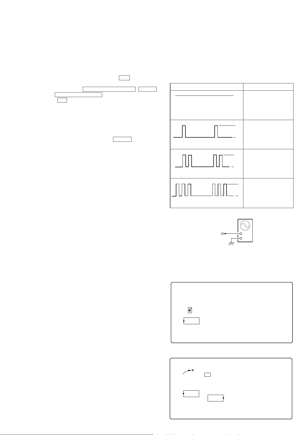
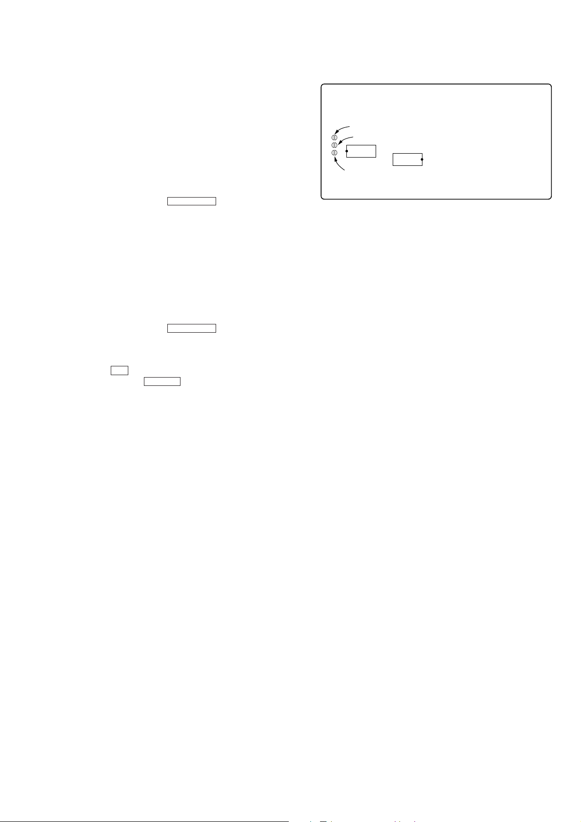
SELF-DIAGNOSIS
This model has the self-diagnosis function for the VIDEO and
AUDIO decoder sections.
Immediately after the power on, the self-diagnosis function searches
each operation of IC’s around the mechanism control microcomputer (IC701).
The results can be checked by connecting an oscilloscope to TP709
(LED) of the VIDEO board.
Oscilloscope (Waveform)
H
Symptom
No error
Light
L
H
External SRAM (IC751)
error
1 time blinking
2-2. Operation during Aging Mode
In the aging mode, the program is executed in the following sequence.
1. A tape on FWD side is played for one minute.
2. PAUSE STOP is made.
3. Recording is made for 3 minutes. (For the deck not having
the record function, the play is executed.)
4. FF is executed up to the end of tape.
5. A tape is reversed, and the tape on REV side is played for
one minute.
6. PAUSE STOP is made.
7. Recording is made for 3 minutes. (For the deck not having
the record function, the play is executed.)
8. FF is executed up to the end of tape.
9. Steps 1 through 8 are executed for the other deck.
10. Steps 1 through 9 are repeated unless an alarm occurred.
2-3. Deck Selection Sequence
• During the aging mode, decks are selected in the following sequence:
Deck A (FWD) → Deck A (REV)
↑↓
Deck B (REV) ← Deck B (FWD)
MPEG decoder (IC201)
error
H
DRAM (IC251) error
3 time blinkin
VIDEO board
TP709 (LED)
L
oscilloscop
+
–
Note: The LED for check (D701) is mounted to some sets
(FORMER TYPE). In this case, confirm the lighting condition of LED.
[VIDEO BOARD] (SIDE A)
[VIDEO BOARD] (SIDE B)
TP709 (LED)
IC751
— 5 —
X901
IC251
Page 6
Front Panel
SECTION 2
GENERAL
%¡
%º
!∞
!¢
!£
!™
!¡
#¶
#§
#∞
#¢
12
#£
34
!¶!§
#¡ #º @ª @• @¶
#™
!•
!ª
5
6
@º
@§
78
@¡
9
0
@™
@£
@¢
@∞
#•
#ª
$ª
$•
$¶
&™
&¡
&º
^ª
^•
$§
%¶
$º
$¡
$™
$£
$¢$∞
%•
%™
%£
%¢
%∞
%§
^º
%ª
^¡
^¶ ^§ ^∞
^¢
— 6 —
^£
^™
Page 7
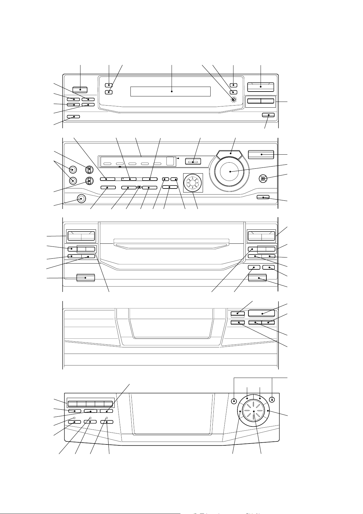
LOCATION OF PARTS AND CONTROLS
1 POWER button
2 DISPLAY/DEMO button
3 SPECTRUM ANALYZER button
4 Display Window
5 ENTER/NEXT button
6 TUNER MEMORY button
7 TUNING MODE button
8 TUNER/BAND button
9 TUNING (+/–) button
!º STEREO/MONO button
!¡ SLEEP button
!™ DAILY 2 button
!£ DAILY 1 button
!¢ t/CLOCK SET button
!∞ REC button
!§ WAVE button
!¶ DSP button
!• Equalizer indicators
!ª PRO LOGIC button
@º EFFECT button
@¡ GROOVE button
@™ FUNCTION button
@£ VOLUME control
@¢ SUPER WOOFER button
@∞ SUPER W MODE button
@§ GEQ control buttons
@¶ GEQ CONTROL button
@• ENTER button
@ª P FILE MEMORY button
#º # button
#¡ KEY CONTROL indicator
#™ ˜ button
#£ KARAOKE PON/MPX button
#¢ PHONES jack
#∞ ECHO LEVEL knob
#§ MIC 1, MIC 2 jacks
#¶ MIC LEVEL knob
#• Deck B ª, · button
#ª Deck B 0, ) button
$º Deck B r REC button
$¡ Deck B P button
$™ CD SYNC button
$£ Deck B 6 EJECT button
$¢ H SPEED DUB button
$∞ Deck B p button
$§ Deck A 0, ) button
$¶ Deck A 6 EJECT button
$• DOLBY NR button
$ª DIRECTION button
%º Deck A p button
%¡ Deck A ª, · button
%™ 6 OPEN button
%£ CD · button
%¢ CD p button
%∞ CD P button
%§ DISC SKIP button
%¶ CD FLASH button
%• 1/ALL DISCS button
%ª PLAY MODE button
^º CD 0, ) button
^¡ REPEAT button
^™ ≠ AMS ± dial
^£ EDIT button
^¢ NEXT button
^∞ AUTO PBC indicator
^§ PREV button
^¶ PBC indicator
^• ˆ RETURN button
^ª VCD indicator
&º CD LOOP button
&¡ CD NON-STOP button
&™ DISC1-DISC5 buttons
SECTION 3
DISASSEMBLY
Note: Follow the disassembly procedure in the numerical order given.
3-1. FRONT PANEL
1
Three flat type wires
(CN401, CN402, CN701)
3
Front panel
2
— 7 —
Four screws (BVTP3x8)
Page 8
3-2. MAIN BOARD
9
Connector
(CN601)
0
Connector
(CN9001)
4
Power cord
5
Back panel
3
Seven screws (BVTP3x8)
2
Eleven screws
(BVTP3x8)
1
Flat type wire (CN1)
Installing the power cord for the
Chinese model.
Power transformer
Bushing cord
Ferrite core
Wire clamp
!£
MAIN board
6
Connector
(CN961)
7
Flat type wire
(CN801)
3-3. TAPE MECHANISM DECK
3
Three screws
(BVTP2.6x8)
A
!¡
Two screws
(BVTP3x8)
4
Three screws (BVTP2.6x8)
5
Remove the tape mechanism deck
section to direction of the arrow
!™
Connector
(CN901)
8
Connector
(CN830)
2
A
.
Open the cassette lids.
1
Push the two buttons.
— 8 —
Page 9
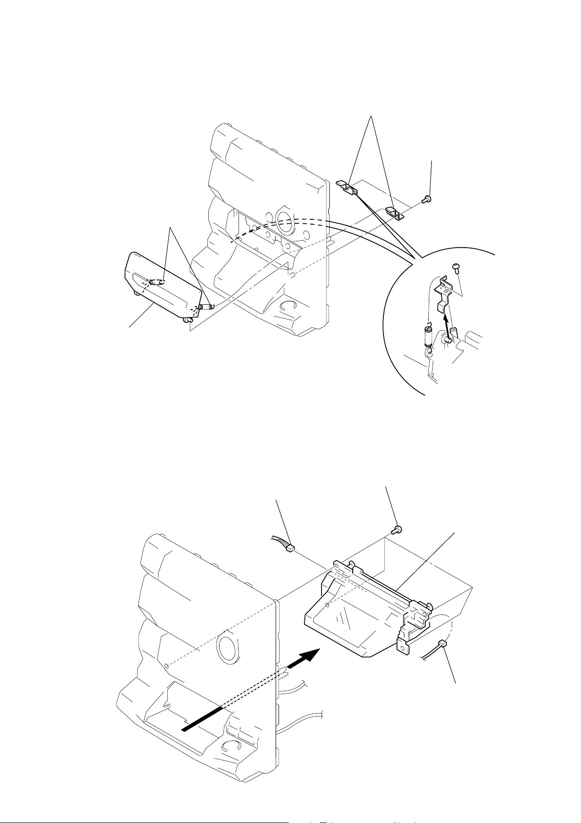
3-4. CASSETTE LID ASSEMBLY
1
Two springs
4
Cassette lid assembly
3
Two bracket
2
Two screws (BVTP2.6x8)
3-5. CD LID ASSEMBLY
2
Connector (CN671)
1
Four screws (BVTP2.6x8)
4
CD lid assembly
3
Connector (CN661)
— 9 —
Page 10
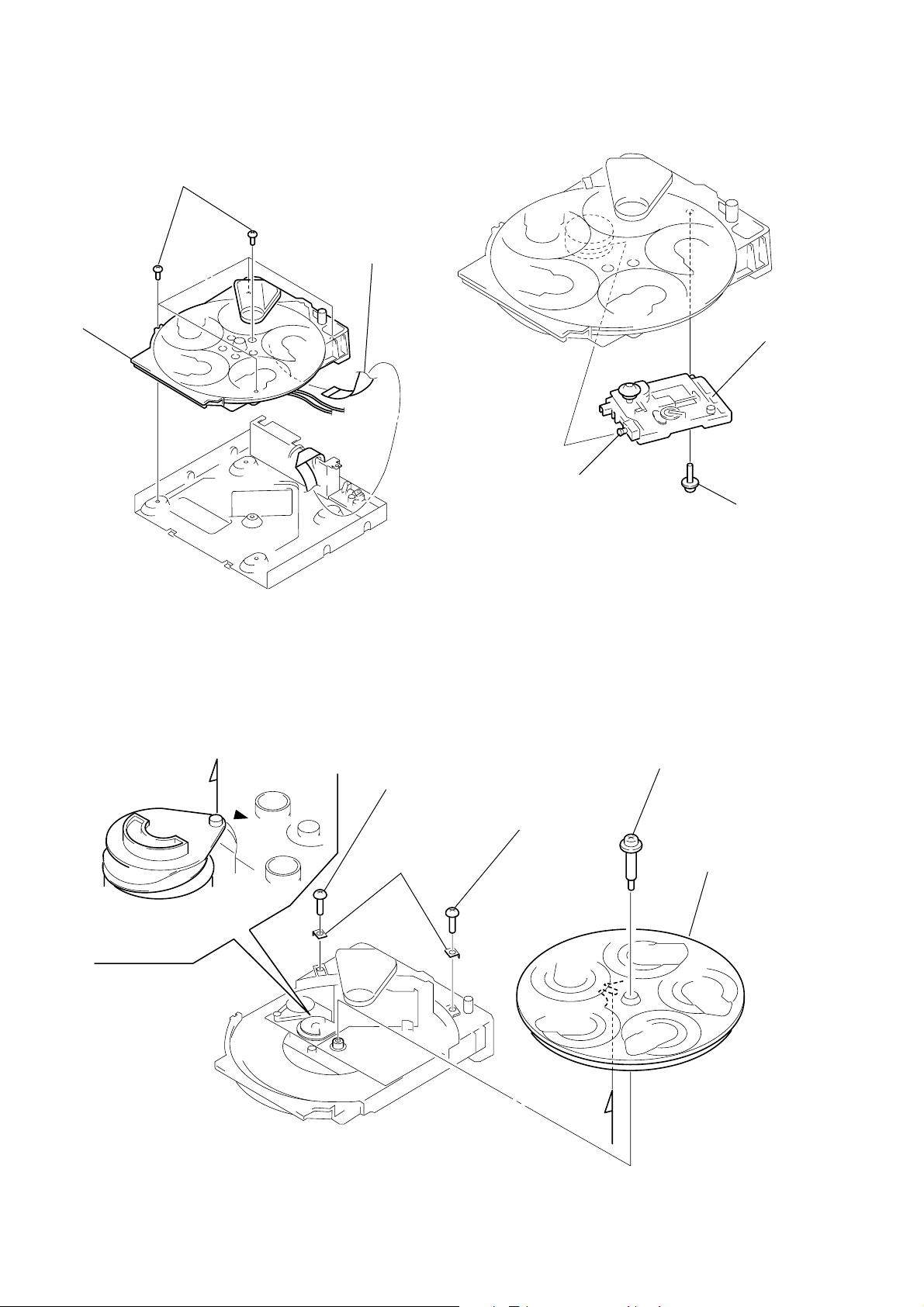
3-6. CD MECHANISM DECK
t
1
Five screws
(BVTP3x8)
2
CD mechanism
deck
3
Flat type wire
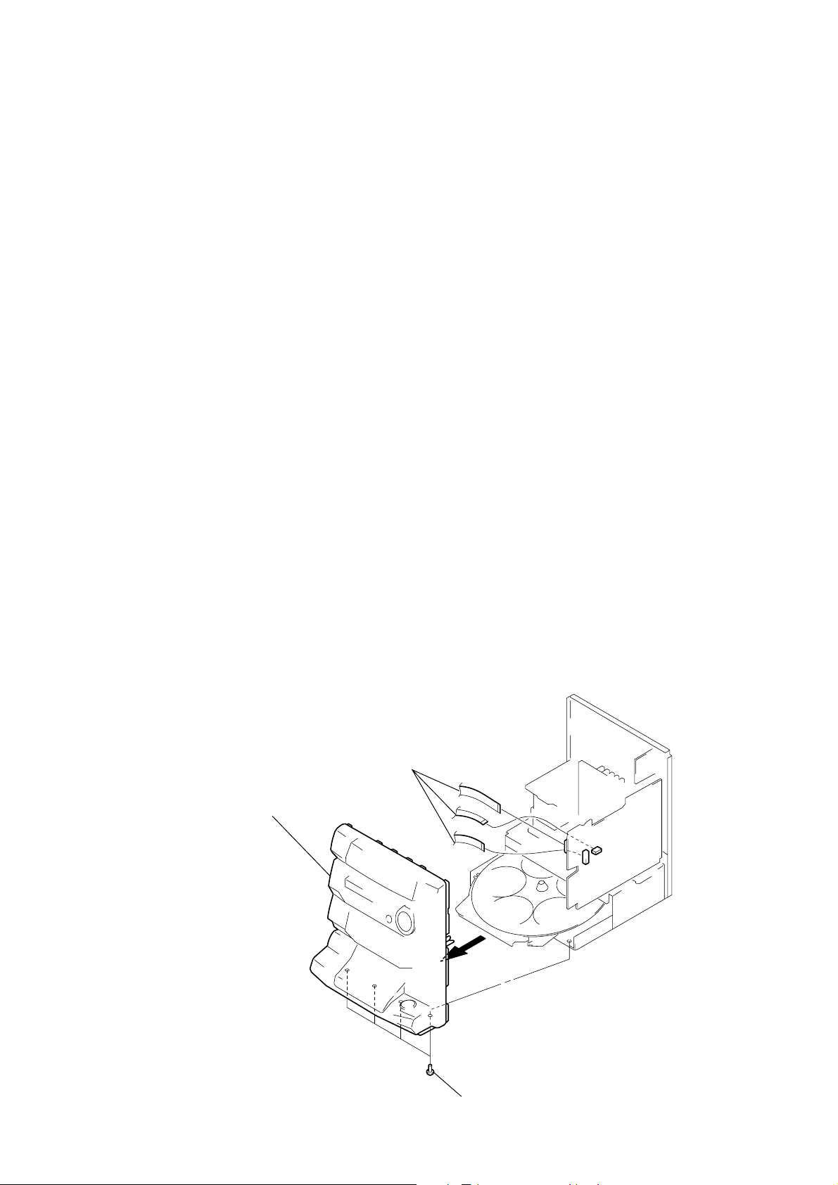
3-7. BASE UNIT
2
Boss
3
Base uni
1
Yoke bracket
3-8. DISC TABLE
Note:
When the disc table is installed, adjust the positions of
roller cam and mark ” as shown in the figure, then set to
the groove of disc table.
A
3
2
Screw (BVTP3x8)
Bracket (BU)
1
Screw (BVTP3x8)
A
4
Stop screw
5
Disc table
— 10 —
Page 11
SECTION 4
SL703 (AFADJ)
IC751
IC251
SL702 (ADJ)
SL701 (CAL BAR)
TEST MODE
VIDEO CD COLOR-BARS MODE
On this mode, the data of the color-bars signal as a picture signal
and the 1kHz sine wave signal as a sound signal are output by the
mechanism control microcomputer (IC701) for video CD signal
check. When measurement of the voltage and waveform on the
VIDEO board, perform it in this mode.
For refernce, the color-bars signal can be observed at J9001 (VIDEO
OUT) and the sound signal can be observed at J101 (VIDEO (AUDIO) OUT) using an oscilloscope.
1. Connect the lead wire to both ends of the land of SL701 (CAL
BAR) of the VIDEO board.
2. Turn the power on. Press FUNCTION button to select CD.
3. After 2 or 3 seconds later, connect the lead wire.
4. After measuring, remove the lead wire connected.
NOTE:
The 1 kHz sine wave is not outputted when the CD is played once,
but it is not error.
E-F BALANCE MODE
• Refer to SECTION 6 ELECTRICAL ADJUSTMENTS page 15.
1. Connect the lead wire to both ends of the land of SL702 (ADJ)
and SL703 (AFADJ) of the VIDEO board.
2. Turn the power on. Press FUNCTION button to select CD.
3. Short-circuit the lead wire. (At this time, “DISC” on the fluores-
cent indicator tube will blink (test mode). If it is not blinking,
perform from step 1 again.)
4. Press the · button in playback.
5. Every pressing the REPEAT b utton, the tracking serv o and the
sledding servo are turned on or off.
6. When the servo is OFF, the counter on front panel will not be
changed.
7. After measuring, remove the lead wire connected step 1.
[VIDEO BOARD] (SIDE B)
— 11 —
Page 12
SECTION 5
MECHANICAL ADJUSTMENTS
SECTION 6
ELECTRICAL ADJUSTMENTS
Precaution
1. Clean the following parts with a denatured alcohol-moistened
swab:
record/playback heads pinch rollers
erase head rubber belts
capstan idlers
2. Demagnetize the record/playback head with a head demagnetizer.
3. Do not use a magnetized screwdriver for the adjustments.
4. After the adjustments, apply suitable locking compound to the
parts adjusted.
5. The adjustments should be performed with the rated power supply voltage unless otherwise noted.
Torque Measurement
Torque
FWD
FWD
back tension
REV
REV
back tension
FF/REW
FWD tension
REV tension
Torque meter
CQ-102C
CQ-102C
CQ-102RC
CQ-102RC
CQ-201B
CQ-403A
CQ-403R
Meter reading
36 to 61 g • cm
(0.5 - 0.84 oz • inch)
2 to 6 g • cm
(0.02 - 0.08 oz • inch)
36 to 61 g • cm
(0.5 - 0.84 oz • inch)
2 to 6 g • cm
(0.02 - 0.08 oz • inch)
61 to 143 g • cm
(0.85 - 1.99 oz • inch)
100 g or more
(3.53 oz or more)
100 g or more
(3.53 oz or more)
DECK SECTION 0 dB=0.775V
1. Demagnetize the record/playback head with a head damagnetizer .
2. Do not use a magnetized screwdriver for the adjustments.
3. After the adjustments, apply suitable locking compound to the
parts adjusted.
4. The adjustments should be performed with the rated power supply voltage unless otherwise noted.
5. The adjustments should be performed in the order given in this
service manual. (As a general rule, playback circuit adjustment
should be completed before performing recording circuit adjustment.)
6. The adjustments should be performed for both L-CH and R-CH.
7. Switches and controls should be set as follows unless otherwise
specified.
Tape
P-4-A100
WS-48B
P-4-L300
NOTE:
Set the test mode by following step before performing the adjustment of “DECK SECTION”. All effects for the output signal are
canceled. If the adjustment is not performed in this test mode, you
cannot adjust correctly.
Procedure :
With the power turned ON, press the SPECTRUM ANALYZER
button, ENTER button, and EFFECT button simultaneously.
(The “VOLUME” on the fluorescent display tube will blink while
in the test mode.)
To exit the test mode, press the POWER button.
Signal
10 kHz, –10 dB
3 kHz, 0 dB
315 Hz, 0 dB
Used for
Azimuth Adjustment
Tape Speed Adjustment
Level Adjustment
Record/Playback Head Azimuth Adjustment
(Deck A, Deck B)
Note: Perform this adjustments for both decks.
Procedure:
1. Mode : Playback
test tape
P-4-A100
(10kHz, –10dB)
set
VIDEO(AUDIO)
OUT
level meter
+
–
— 12 —
Page 13
2. Turn the adjustment screw and check output peaks. If the peaks
e
do not match for L-CH and R-CH, turn the adjustment screw so
that outputs match within 1 dB of peak.
L-CH
peak
output
level
within
1 dB
within 1dB
Tape Speed Adjustment (Deck A)
Note: Set the test mode using the following method and begin tape
speed adjustment.
In the test mode, the tape will move at double speed while
the H SPEED DUB button is pressed.
Procedure :
With the power turned ON, press the SPECTRUM ANALYZER
button, ENTER button, and EFFECT button simultaneously.
(The “VOLUME” on the fluorescent display tube will blink while
in the test mode.)
To exit the test mode, press the POWER button.
R-CH
screw
position
peak
3. Mode: Playback
test tape
P-4-A100
(10kHz, –10dB)
in phase 45
L-CH
peak
VIDEO
(AUDIO)
OUT
L
set
R
Waveform of oscilloscope
°
90
°
good
135
R-CH
peak
°
oscilloscope
180
wrong
°
screw
position
1. Load WS-48B into deck A and a recordable tape into deck B.
2. Press the r REC button, and press the · button of deck B to
set deck B into the recording state.
3. Play deck A.
4. While pressing the H SPEED DUB button, set double speed
play.
5. Adjust RV652 of the AUDIO board so that the reading of the
frequency counter becomes 6000 ± 90 Hz.
6. Release the H SPEED DUB button to set normal speed play.
7. Adjust RV651 of the AUDIO board so that the reading of the
frequency counter becomes 3000 ± 90 Hz.
Adjustment Location: AUDIO board
Sample Value of Wow and flutter
W.RMS (JIS) less than 0.3%
(test tape: WS-48B)
Playback Level Adjustment (Deck A, Deck B)
Procedure:
Mode: Playback
test tape
P-4-L300
(315Hz, 0dB)
set
level meter
4. After the adjustments, apply suitable locking compound to the
parts adjusted.
Adjustment Location: Playback Head (Deck A)
Record/Playback/Erase Head (Deck B)
revers
forward
VIDEO
(AUDIO)
OUT
Deck A is RV311 (L-CH) and RV411 (R-CH), deck B is RV301
(L-CH) and RV401 (R-CH)
so that adjustment within the following adjustment level.
Adjustment level:
CN403 playback level: 301.5 to 338.3 mV (–8.2 to –7.2 dB)
level difference between the channels: within ± 0.5 dB
Adjustment Location: AUDIO board
— 13 —
Page 14
Record Bias Adjustment (Deck B)
)
Record Level Adjustment (Deck B)
Procedure:
INTRODUCTION
When set to the test mode performed in Tape Speed Adjustment, when the tape is rewound after recording, the “REC memory
mode” which rewinds only the recorded portion and playback is
set.
This “REC memory mode” is convenient for performing this adjustment. During recording, the input signal FUNCTION will automatically switch to VIDEO.
1. Press FUNCTION button to select VIDEO. (This step is not
necessary if the above test mode has already been set.)
2. Load a tape into deck B, and press the r REC button.
3. Mode: Record
VIDEO (AUDIO) IN
1) 315Hz
2) 10kHz
AF OSC
attenuator
} 50 mV (–23.8 dB)
600
Ω
blank tape
CS-123
set
4. Mode: Playback
recorded
position
level meter
Procedure:
INTRODUCTION
When set to the test mode performed in Tape Speed Adjustment, when the tape is rewound after recording, the “REC memory
mode” which rewinds only the recorded portion and playback is
set.
This “REC memory mode” is convenient for performing this
adjustment. During recording, the input signal FUNCTION will
automatically switch to VIDEO.
1. Press FUNCTION button to select VIDEO. (This step is not
necessary if the above test mode has already been set.)
2. Load a tape into deck B, and press the r REC button.
3. Mode: Record
VIDEO (AUDIO) IN
315Hz 50 mV (–23.8 dB)
AF OSC
attenuator
600
Ω
set
blank tape
CS-123
4. Mode: Playback
recorded
position
level meter
set
VIDEO
(AUDIO)
OUT
5. Confirm playback the signal recorded in step 2 become adjustment level as follows.
If these levels do not adjustment level, adjust the RV341 (LCH) and RV441 (R-CH) on the AUDIO board to repeat steps 3
and 4.
Adjustment level: The playback output of 10 kHz le vel dif ference
against 315 Hz reference should be ± 1.0 dB.
Adjustment Location: AUDIO board
Adjustment Location
[AUDIO BOARD] (Conductor Side)
RV341 (Lch), RV441 (Rch)
Record Bias
RV301
RV401
RV441 RV341
RV301 (Lch), RV401 (Rch)
Playback Level (Deck B)
RV651 (Normal Speed)
RV652 (High Speed)
Tape Speed
RV311 (Lch), RV441 (Rch)
Playback Level (Deck A)
RV651
RV311
RV411
RV652
set
VIDEO
(AUDIO)
OUT
5. Confirm playback the signal recorded in step 2 become adjustment level as follows.
If these levels do not adjustment level, adjust the RV301 (LCH) and RV351 (R-CH) on the MAIN board to repeat steps 3
and 4.
Adjustment level:
CN403 playback level: 47.2 to 53.0 mV (–24.3 to –23.3 dB)
Adjustment Location: MAIN board
RV301
[MAIN BOARD] (Component Side)
Record Level (L CH
IC401
RV351
Record Level
(R CH)
— 14 —
Page 15
CD SECTION
NOTE :
1. CD Block is basically designed to operate without adjustment.
Therefore, check each item in order given.
2. Use YEDS-18 disc (3-702-101-01) unless otherwise indicated.
3. Use an oscilloscope with more than 10MΩ impedance.
4. Clean the object lens by an applicator with neutral detergent when
the signal level is low than specified value with the following
checks.
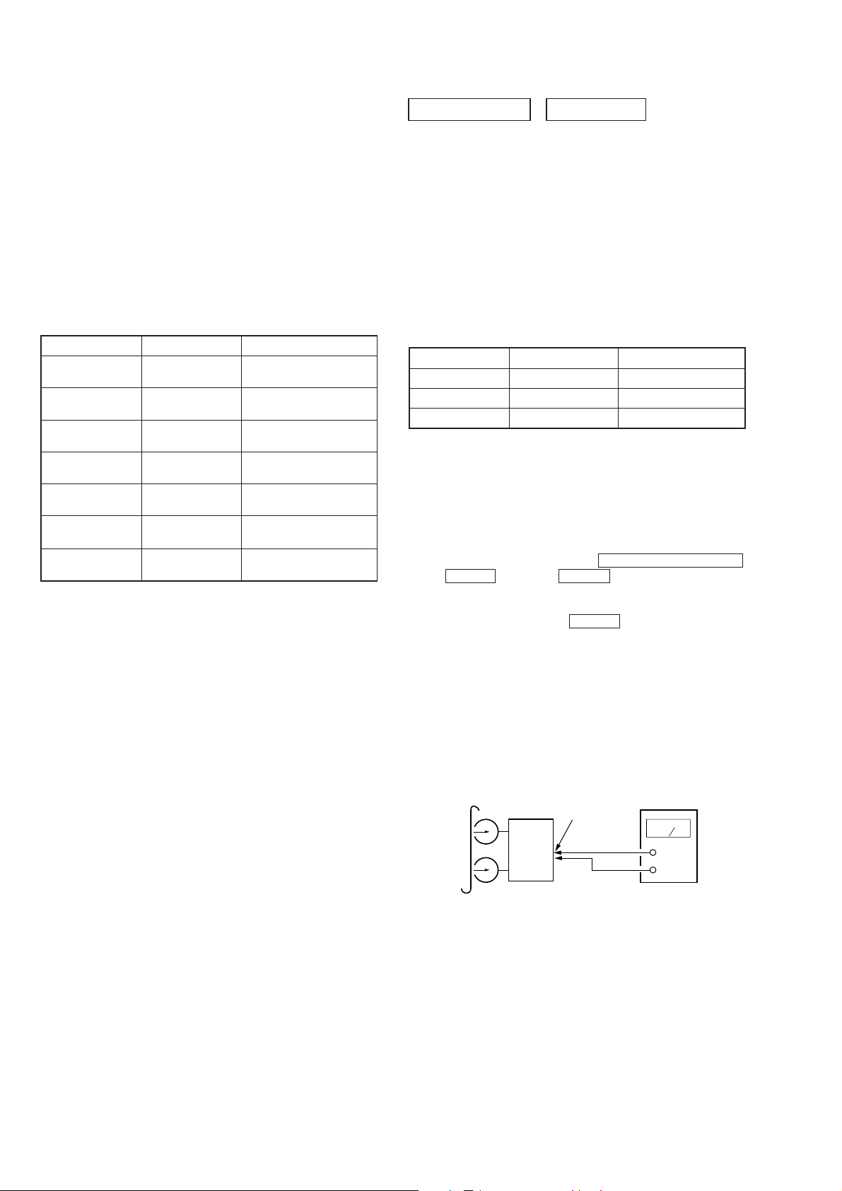
S Curve Check
oscilloscope
BD board
TP (FE)
TP (VC)
Procedure :
1. Connect oscilloscope to test point TP (FE) on BD board.
2. Connect between test point TP (FEI) and TP (VC) by lead wire.
3. Turned Power switch on.
4. Put disc (YEDS-18) in and turned Power switch on again and
actuate the focus search. (actuate the focus search when disc
table is moving in and out.)
5. Check the oscilloscope waveform (S-curve) is symmetrical between A and B.
And confirm peak to peak level within 3±1 Vp-p.
S-curve waveform
+
–
symmetry
A
B
Within 3
±
1 Vp-p
Note : A clear RF signal waveform means that the shape “◊” can
be clearly distinguished at the center of the waveform.
RF signal waveform
VOLT/DIV : 200mV
TIME/DIV : 500ns
level : 1.3 Vp-p
+0.25
–0.20
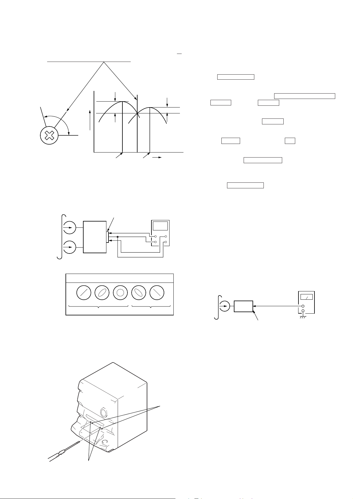
E-F Balance (Traverse) Check
oscilloscope
BD board
TP (TE)
TP (VC)
+
–
Procedure :
1. Connect oscilloscpe to test point TP (TE) on BD board.
2. Connect the lead wire to both ends of the land of SL702 (ADJ)
and SL703 (AFADJ) of the VIDEO board.
3. Turned Power switch on. Press FUNCTION button to select
CD.
4. Short the lead wire.
5. Put disc (YEDS-18) in to play the number five track.
6. Press the REPEAT button. (The tracking servo and the sledding servo are turned OFF.)
7. Check the level B of the oscilliscope's waveform and the A (DC
voltage) of the center of the Traverse waveform.
Confirm the following :
A/B x 100 = less than ± 22%
Traverse waveform
Center of the waveform
6. After check, remove the lead wire connected in step 2.
Note : • Try to measure several times to make sure than the ratio
of A : B or B : A is more than 10 : 7.
• Take swee p time as long as possible and light up the brightness to obtain best waveform.
RF Level Check
oscilloscope
BD board
TP (RF)
TP (VC)
+
–
Procedure :
1. Connect oscilloscope to test point TP (RF) on BD board.
2. Turned Power switch on.
3. Put disc (YEDS-18) in to play the number five track.
4. Confirm that oscilloscope waveform is clear and check RF signal level is correct or not.
B
0V
level : 1.3
A (DC voltage)
±
0.6 Vp-p
8. Press the REPEAT button. (The tracking servo and sledding
servo are turned ON.) Confirm the C (DC voltage) is almost
equal to the A (DC voltage) is step 7.
Traverse waveform
C (DC
0V
Tracking servo
Sled servo
OFF
Tracking servo
Sled servo
ON
voltage)
9. Remove the lead wire connected step 1.
— 15 —
Page 16
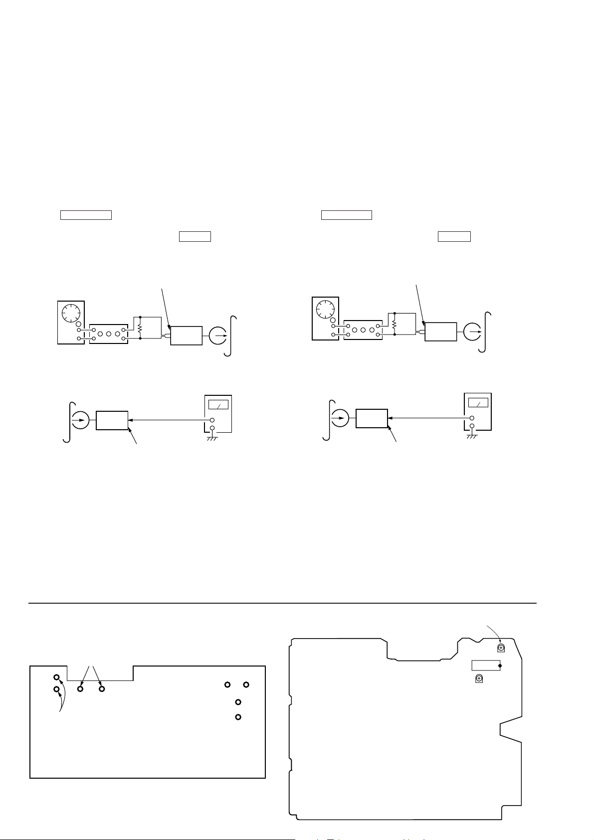
RF PLL Free-run Frequency Check
Procedure :
1. Connect frequency counter to TP (PLCK) with lead wire.
VIDEO SECTION
Frequency adjustment
BD board
TP (PLCK)
frequency counter
+
–
2. Turned Power switch on.
3. Put the disc (YEDS-18) in to play the number five track.
Confirm that reading on frequency counter is 4.3218MHz.
1. Connect the frequency counter to check point of the VIDEO
board.
frequency counter
VIDEO board
TP410 (DCLK)
+
–
2. Adjust CT401 of the VIDEO board so that the frequency counter
read 13.5MHz ± 40Hz at STOP condition.
Adjustment Location :
[ BD BOARD ] — SIDE A — [ VIDEO BOARD ] — SIDE B —
1
10 11
(PLCK)
IC103
IC101
20
(VC)
(RF)
(TE)
(FE)
(FEI)
SL703 (AFADJ)
SL702 (ADJ)
IC751
SL701 (CAL BAR)
CT401
Frequency
IC251
TP410 (DCLK)
— 16 —
Page 17
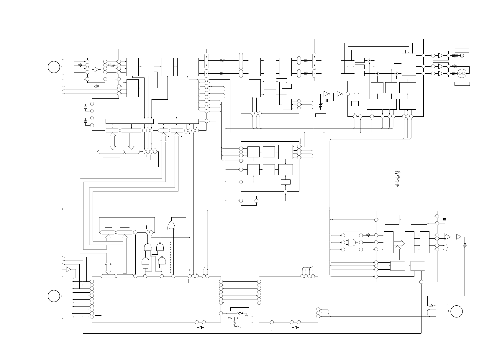
7-1. CIRCUIT BOARDS LOCATION
d
d
PANEL board
HP/MIC board
TC-A SW board
CD-LED board
SECTION 7
DIAGRAMS
TRANS board
VIDEO POWER board
FM/AM TUNER PACK
SURROUND boar
MAIN board
7-2. BLOCK DIAGRAMS
— KEY CON SECTION —
J761
MIC 1
J762
MIC 2
MIC AMP
IC760 (1/2)
31
RV760
MIC LEVEL
1
LPF1
ECHO AMP
IC760 (2/2)
67
ECHO
IC761
2
9
LPF2
8
RV761
ECHO LEVEL
HCD-V8800
CD-A SW board
DOOR SW board
TC-B SW board
Note: pA is including in AUDIO board.
AUDIO board
(including
p
A)
TABLE SENSOR board
CD-B2 SW board
CD-B1 SW board
p
A
MOTOR board
POWER board
VIDEO OUT board
VIDEO board
KEY CON board
LEAF SWITCH boar
BD board
SWITCH
IC1403
5
3
KEY CONTROL
IC1401
STORBE
9
MIX
OUT
15
Q1401
LPF1
IN
22
Rch
09
DATA
78
CLOCK
4
91011
• R CH : Same as Lch
L IN
K CON
LATCH
CLK
DATA
L OUT
A
MAIN
SECTION
(Page 25)
• Signal path
: FM
: MIC
CD MOTOR board
LED board
— 17 —
— 18 —
Page 18
HCD-V8800
— CD SECTION —
OPTICAL PICK-UP
BLOCK (KSS-213D/Q-NP)
LASER
DIODE
LD
POWER
PD
LD
DETECTOR
E
AC
BD
F
1
TRACKING
COIL
FOCUS
COIL
4
M102
SLED
MOTOR
M101
SPINDLE
MOTOR
DRIVE
Q101
RF AMP
IC103
APC LD
2
AMP
LD
1
3
4
5
6
8
9
VC
T+
T–
F+
F–
M
M
SUMMING
TRACKING
ERROR
FOCUS/TRACKING COIL DRIVE
SPINDLE/SLED MOTOR DRIVE
1
2
16
17
13
12
27
26
09
AMP
AMP
RF
FOCUS
ERROR
BUFFER
AMP
VC
IC102
RF FQ
AMP
19
RF
16
15
13
1110
VC
12
4
5
19
20
10
9
23
24
15MUTE
INTEGRATOR
INTE-
GRATOR
DIGITAL SERVO
DIGITAL SIGNAL PROCESSOR
IC101
ASY0
39
RF AC
36
ASY1
38
26
27
28
29
10
100
96
ASYMMETRY
CORRECTION
RF DC
TE
A/D
SE
CONVERTER
FE
TFDR
4
TRDR
6
FFDR
8
FRDR
SRDR
2
SFDR
MDP
MIRR
DFCT
FOK
DETECTOR
62
XTAL
CLOCK
GENERATOR
PLL
EFM
DEMODULATOR
SYNC
PROTECTOR
TIMING
GENERATOR 1
CLV SERVO
PROCESSOR
1B TIMS
OVERSAMPLING
FILTER
NOISE
SHAPER
REGISTER
CORRECTOR
GENERATOR 2
MIX
DIGITAL
FOK
DFCT
MIRR
SERVO DSP
FOCUS
SERVO
TRACKING
SERVO
SLED
SERVO
PWM
GENERATOR
TRACKING
PWM
GENERATOR
FOCUS
PWM
GENERATOR
SLED
PWM
GENERATOR
ERROR
TIMING
DATA BUS
PRIORITY
EMCODER
ADDRESS
GENERATOR
32K
RAM
D/A
DATA
PROCESSOR
MUTE
79 54
M201
TABLE
MOTOR
MD2
70
DOUT
S201
UP SW
EXCK
SBSO
SUBQ
SQCK
SCLK
DATA
LRCK
BCLK
SCOR
WFCK
DATA
SENS
C2PO
DFCT
MIRR
XRST
71
76
75
77
78
83
46
45
47
74
73
86
XLT
87
CLK
88
80
56
FOK
93
92
91
81
DIGITAL
OUT
PEAK
DETECTOR
SERIAL/PARALLEL
PROCESSOR
GFS
S STOP
99
+5V
7
M
3
SERVO
INTERFACE
S901
LIMIT
SWITCH
MOTOR DRIVER
IC201
OUT1
OUR2
SUBCODE
P-W
PROCESSOR
SUBCODE
Q
PROCESSOR
INTERFACE
SEQUENCER
IN1
9
1
IN2
CPU
SERVO
AUTO
DISC
TABLE
SENSOR
IC202
LDON
+5V
384FS
SUBQ
SQCK
SCLK
ADATA
LRCK
BCK
SCOR
B
DATA
VIDEO
XLT
SECTION
CLK
(Page 21)
SENS
C2PO
XRST
AMUTE
UP SW
T.SENS
C
MAIN
SECTION
(Page 25)
TBL.L
TBL.R
— 19 —
• R CH: Same as L ch
• SIGNAL PATH
: CD
: VIDEO
— 20 —
Page 19
HCD-V8800
— VIDEO SECTION —
BCK
ADATA
LRCK
B
C2PO
CD
SECTION
(Page 20)
SECTION
(Page 20)
09
384FS
ADATA
LRCK
BCLK
X202
28.63636MHz
X201
45.1584MHz
DATA
CLK
AMUTE
384FS
416
IC501
(2/2)
384FS
DATA
CLK
AMUTE
SQCK
SUBQ
B
SCLK
XLT
CD
LDON
SCOR
SENS
XRST
9
8
7
6
5
BUFFER
IC501 (1/2)
2
3
106
107
73
78
74
11
10
77
76
75
71
62
48
11
12
13
14
15
XTL0O
XTL01
XTL2O
XTL2I
38–43 46–55•
2–5 7–10 35–38 40–43
•
•
DQ1
I/O1
•11–13 15–19
D0
DATA
CLK
AMUTE
SQCK
SUBQ
SCLK
XLT
LDON
SCOR
SENS
RESET
112
111
110
109
103
100
101
102
D-RAM INTERFACE
•
A0
I/O8
2–10 21 23–25
21–29 • 31–3513 – 20
A0
D7
CD-ROM
DECODER
MPEG
AUDIO
DECODER
17–21 23 24 32 33••••
18–21 24–28•
A0
DQ16
D-RAM
IC251
S-RAM
IC751
A12
OE
••
55
RD
A12
MPEG DECODER
IC201
POSTPROCESSOR
SYNC GENERATOR
HOST INTERFACE
5 6•• •119 120
D0
D7
XTCS
AS
VIDEO
&
A0
A3
XHCS
XWR
WR
3735
7–13 16
301516 31
W
LCAS
UCAS
IC772
WE
CE1
272022
6
54
3
12
13
40
MECHA CONTROL
IC701
MPEG
VIDEO
DECODER
EACH CIRCUIT BLOCK
•
IC771
A17
MPEG
SYSTEM
DECODER
34
A8
RAS
8
10 9
11
12
41 54 56 43 70 7 8
A18
XHDT
WAIT
117115116114
XHIRQ
XHIRQ
EXTAL
Y
C
5251
71
74
•
76
80
63
70
97
95
92
93
94
89
56
57
58
59
XRST
118
GENERATOR
DF-XLAT
VDAC-XLAT
XTAL
X701
10MHz
XSGRST
HSYNC
VSYNC
FID
DCLK
XOSDEN
OSD B
OSD G
OSD R
CLOCK
IC272
CMD0
CMD1
CMD2
CMD3
SACK
QINT
MREQ
NPIN
Y0-Y7
C0-C7
1
2
3
4
5
6
72
64
OSD B
OSD G
OSD R
XOSDEN
VSYNC
HSYNC
DCLK
SYSTEM SELECT
1
4
Y
•
6
9
11
C
18
18
17
16
15
19
20
CK 1/2 Q
1 5
S9001
RGB-YUV
CONV.
TIMING
GEN.
98 10097
HSYNC
OUTPUT
CONT.
SYNC
CONT.
PAL
AUTO
NTSC
NOISE REDUCTION
DCLKI
VSYNC
DCLK
34
CMD0
35
CMD1
36
CMD2
37
CMD3
44
SACK
18
QINT
MREQ
43
IC301
NOISE
REDUSER
MEMORY
CONT.
OSD
IC271
VIDEO
RAM
DATA
SEL.
6.75MHz
CD-XRST
YUV-RGB
CONV.
DRAM
IF
DATA INPUT
SHIFT
RESISTOR
DISPLAY
POSITION
CONT.
OSC
8
IIC INTERFACE
IC901
10BIT VIDEO D/A CONVERTER
IC401
VIDEO AMP
1
60
4
•
67
51
58
NR-XCS
29
MCLK
30
MDATA
31
RESET
4
MDATA
3
OS-XLAT
2
MCLK
1
MDATA
X2
X1
111052
X901
5MHz
MCLK
OS-XLAT
RESET
IIC-DATA
IIC-CLK
11
18
68494847
6
9
13.5MHZ
NR-XCS
15
55
56
DEMPX, LEVEL
TRANSLATOR
INTERPOLTATOR
CLOCK GENARATOR
3
X401
27MHz
CT401
XRST
&
IC402
56
4
384FS
ADATA
LRCK
BCLK
DATA
CLK
DF-XLAT
AMUTE
LPF
LPF
DELAY
56
1/2
DCLK
BUFFER
IC181
11
13
4
1
6
3
XRST
MODULATOR
SYNC
SUB
SLOPE
CARRIER
GEN.
GEN.
SYNC GEN.
&
TIMING CONT.
XVRST
FID
VSYNC
HSYNC
• R CH: Same as L ch
• SIGNAL PATH
: VIDEO
: Y
: CHROMA
: CD
DIGITAL FILTER & D/A CONVERTER
TIMING
6
CIRCUIT
11
INPUT PLM
12
10
3
4
5
2
MODE
Y, C/Y, U, V
SELECTOR
&
INTER-
POLATOR
CLOSED
CAPTION
ENCODER
SIO & I2O-BUS
CONT.
49 504859 60625557 51
CLK
DATA
IC101
D/A
CONV.
V
Y
C
VDAC-XLAT
CLOCK
GENERATOR
MUTE
CIRCUIT
24
29325
INT
1
IC451
5 7
3
Y/C AMP
IC452
21
22
27
25
16
18
L CH
XRST
IIC-DATA
IIC-CLK
2
3
7
1
X101
33.8688MHz
ACTIVE LPF
IC102
16 7
R CH
SECTION
(Page 25)
J9001
VIDEO OUT
4
J9002
S VIDEO OUT
D
MAIN
3
— 21 —
— 22 —
Page 20
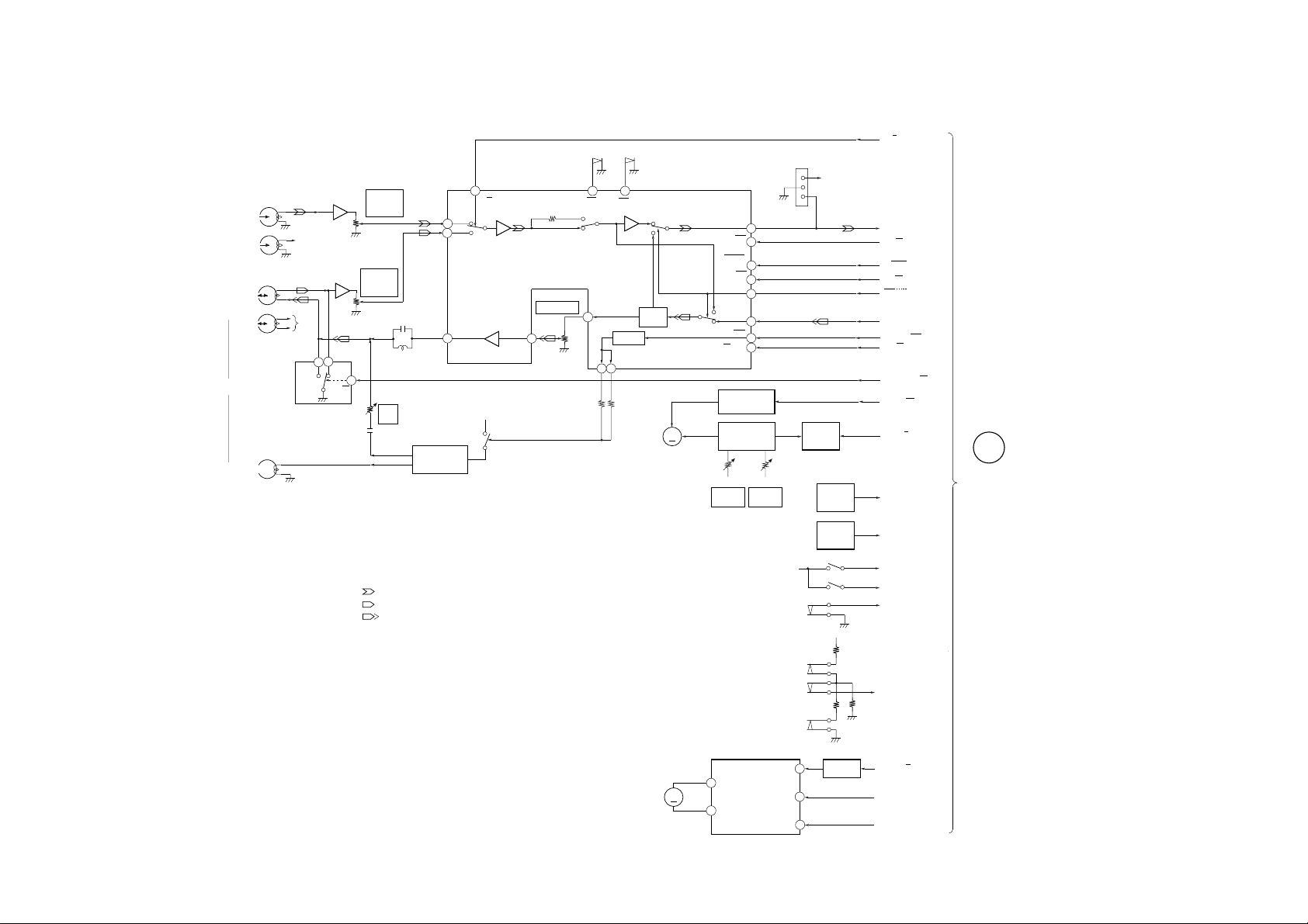
HCD-V8800
— DECK SECTION —
HP101
PB HEAD
(DECK A)
REC/PB HEAD
(DECK B)
HRPE101
ERASE HEAD
S1008
S1004
B CrO
2
DOLBY NR
RECOUT
NORM
24 25
15
B 120/70
BIAS SW
CROM
2
PAS
DOL
M1
CAPSTAN
MOTOR
DOLBY
TYPE B
CN403
3
R CH
1
PB OUT
8
LM ON/
20
OFF
NORM/
14
HIGH
NR ON/
18
OFF
19
PB
RIN
6
BIAS ON/OFF
16
17
RM ON/OFF
CAP M SWITCH
Q405, 407
SPEED
RV651
NORMAL
SPEED
CONTROL
Q651
RV652
HIGH
SPEED
M
+5V
S1003
(A HALF)
SWITCH
Q406
REEL
DETECT
Q1001
REEL
DETECT
Q1002
S1001 (A PLAY)
S1002 (B PLAY)
+5V
A CrO
RV311
RV301
PLAYBACK
IC601
DECK B
1
IC602
R
4
REC/PB
• R CH : Same as L ch
• SIGNAL PATH
: PB (DECK A)
: PB (DECK B)
: REC (DECK B)
PLAYBACK
LEVEL
DECK A
LEVEL
RV341
REC
BIAS
REC BIAS
T621, Q621, 622
IC611
L
R
R CH
L
R
R CH
3
P
ERASE BIAS
X
BIAS OSC
12
PB-A/B
A IN
2
B IN
4
+7.5V
Q623, 901
EQIN
10
EQOUT
11
RV301
REC LEVEL
13
A 120/70
70
120
DECK PROCESS
IC401
10
PB A/B
PB L
LM ON/OFF
NORM/HIGH
NR ON/OFF
REC/PB/PASS
REC L
BIAS ON/OFF
RM ON/OFF
RELAY REC/PB
CAP M ON/OFF
CAP M H / L
A SHUT
B SHUT
A PLAY
B PLAY
A HALF
E
MAIN
SECTION
(Page 25)
S1005
TRIGGER
MOTOR
DRIVE
IC402
(REC A)
S1006
(B HALF)
S1009
(REC B)
VZ
IN2
IN1
BHALF
SWITCH
4
Q408, 409
6
5
TRIG H / L
B TRIG
A TRIG
— 24 —
09
2
M2
TRIGGER
MOTOR
M
OUT1
10
OUT2
— 23 —
Page 21
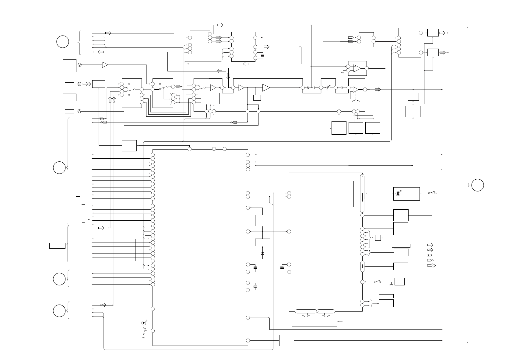
HCD-V8800
— MAIN SECTION —
KEY CON
SECTION
A
(Page 18)
J101
PHONO
IN
L
IN L
VIDEO
J101
(AUDIO)
OUT L
RELAY REC/PB
A SHUT
B SHUT
B HALF
E
DECK
SECTION
(Page 24)
FM/AM
TUNER PACK
ENCAPSLATED
COMPONENT
C
CD
SECTION
(Page 20)
D
VIDEO
SECTION
(Page 22)
09
A HALF
A PLAY
B PLAY
PB A / B
NORM/HIGH
BIAS ON/OFF
RM ON/OFF
NR ON/OFF
REC/PB PASS
LM ON/OFF
CAP M H/L
TRIG H/L
CAP M ON/OFF
COM DIN
COM DATA
STEREO
T. SENS
IIC-DATA
IIC-CLK
DATA
LATCH
K CON
L OUT
PB L
REC L
A TRG
B TRG
TUNED
ST CE
MUTE
TBL. L
TBL. R
UP SW
L CH
XRST
L IN
CLK
ST L
3
4
5
6
31
PHONO EQ AMP
IC101
MUTE
Q121
TC
ST
CD
V
INPUT SELECT
1
2
4
5
MUTE
CONTROL
Q123,124
IC102
INH
D201
(DISC No.)
A
B
D+5V
10
3
9
6
1
2
3
4
5
6
Q201
— 25 —
3
5
96
RELAY
26
A SHUT
27
B SHUT
28
B HALF
97
A HALF
94
A PLAY SW
95
B PLAY SW
87
PB A/B
88
EQ H//N
89
BIAS
90
REC MUTE
91
NR ON/OFF
R/P PASS
92
93
TC MUTE
82
CAP H/N
83
A TRG
84
B TRG
85
TRG LOW
86
CAP M ON/OFF
41
VOL LAT
42
PL LAT
44
45
COM CLK
66
70
TUNED
69
68
ST CE
72
ST MUTE
67
ST DOUT
4
K CON LAT
5
K CON ON
60
TBL L
61
TBL R
UP SW
77
76
T SENS
XRST
57
62
TRAY LED
INPUT SELECT
IC103
COM DOUT
ST DIN
STEREO
10
11
4
9
DOLBY PRO LOGIC
9
L-IN
3
41
DATA
4
42
CLK
2
40
EN
69
71
28
29
30
54
INPUT CHANGE
MASTER CONTROL
IC601
IC701
C-OUT
S-OUT
L-OUT
34
35
37
MICON
INTERFACE
34
32 33
3
4
LATCH
3
427 LAT SW F CON
CENTER
REAR
FRONT
3
4
2
65 64
99
10
8
3
2
4
EN
CD POWER
STK MUTE
DELAY
IC602
S-IN
L-IN
DATA
CLK
POWER
DBFB H/L
TA MUTE
R RELAY
IIC DATA
IIC CLK
RESET
AC CUT
XT1
XT2
FRONT
X1
X2
S-OUT
L-MIX
XTAL
62
98
55
56
11
10
14
13
46
100
OUT
XTAL
REC 2A
2
1
7
15
20
13
16
23
24
EQ
D951
FRONT
61
RESET
SWITCH
Q951
RESET
IC951
+5V
X701
5MHz
X702
32.768KHz
X601
8MHz
X601
8MHz
MUTE
SWITCH
Q912
DATA
28
CLOCK
27
14
RESET
12
XOUT
13
XIN
45 44 43 42
+ +
EQUALIZER / VOLUME
IC201
S.WOOFER
MODE
SWITCH
Q206
DISPLAY CONTROL
IC601
FL601
GR1–16
51 – 66
SEG1–35
67 – 100 • 1
FLUORESCENT INDICATOR TUBE
39
REAR
CENTER
6
5
LED SELECT
SPEANA 1
SPEANA 2
SPEANA 3
SPEANA 4
DOOR SW
VF
40
SWITCH
LED1
LED18
SIRCS
JOG A
JOG B
KEY 5
KEY 1
VOL A
VOL B
DBFB
Q201
L+R
AMP
IC861
BB22
VOLUME
3
IN
14
IN
4
8
CLK
3
9
DATA
1
10
PANEL LED
LED
CONTROL
Q601
REMOTE
CONTROL
RECEIVER
IC602
S711
= AMS +
ROTARY
ENCODER
KEY
MATRIX
S681
6
OPEN
IC604
MUTE
Q254
MUTE
SWITCH
Q120
2
OUT
15
OUTLATCH
IC603
3
1
AMP
7
5
7
FRONT
38
BB12
41
DBFB
SWITCH
Q202
3
10
•
15
•
16
•
18
LED
SWITCH
23
•
25
•
47
29
39
42
43
D/A
44
45
46
26
41
37
33
38
S701
24
40
VOLUME
ROTARY
ENCODER
REAR
MUTE
Q602
MUTE
Q601
Q602,603
CENTER
FRONT
DBFB
POWER ON/OFF
R RELAY
D+5V
REAR
CENTER
• R CH: Same as L ch
• SIGNAL PATH
: FM
: CD
: PB
: REC
: VIDEO
CD POWER
STK MUTE
F
POWER
SECTION
(Page 27)
— 26 —
Page 22
HCD-V8800
— POWER SECTION —
F
MAIN
SECTION
(Page 26)
09
REAR
CENTER
FRONT
DBFB
STK MUTE
R RELAY
CD POWER
POWER ON/OFF
FRONT
POWER AMP
IC201
1 10
6
SWITCHED
AU/D5V SW
TM402
UNREG
–12V
FRONT
Rch
TRANSFORMER
SURROUND
SPEAKER
+3.3V REG
IC801
2 1
T501
POWER
SPEAKER
M
TM401
FRONT
J760
PHONES
REAR
CENTER
M901
FAN
MOTOR
D+5V
(SW)
E,SP,IA,CH
VOLTAGE
SELECTOR
S501
D+5V
(UNSW)
+5V SW
3 1
Q9001
Q9002
• R CH : Same as L ch
• SIGNAL PATH
: FM
• Abbreviation
SP : Singapore model.
AC
IA : Indonesian model.
IN
CH : Chinese model.
+5V REG
IC9001
POWER AMP
OVER LOAD
MUTE
SWITCH
Q331
1
DET
Q601,651
IC601
6
Rch
+5V
D905
D7V
A+7.5V
A–7.5V
+12V
ST 10V
PRO-LOG 10V
10
1318
Rch
Q323
3 1
3 1
+7V, –7V REG
+7.5
1
–7.5 EN
10
+12V REG
3 1
3 1
+10V REG
REAR
CENTER
THERMAL
DET
Q670,671
THP670
OVER LOAD
DET
Q201
Rch
D5V
+5V REG
Q906
Q907
+5V REG
IC902
+7V REG
IC903
IC901
IC904
IC905
RY401
–1
–2
RELAY
DRIVE
Q404
Rch
RY402
–1
RELAY
DRIVE
Q403
RELAY
6
2
PROTECTOR
IC301
1
7
PROTECT
SWITCH
Q301
A+5V
(SW)
V
CC
2
9
V
EE
4
UNREG
–12V
Q901
POWER B+
POWER B–
SURR B+
SURR B–
CONTROL
Q402
HP / SP
SWITCHING
+5V REG
IC9002
3 1
VFDP
Q401,405
D302,303
VF REG
Q941
RECT
4
+5V SW
Q9003
Q9004
RECT
D901
RECT
D101
RECT
D102
CENTER
FAN MOTOR
DRIVER
Q961, 962
RECT
D104,105
REAR
D+3.3V
VF
VF
— 27 — — 28 —
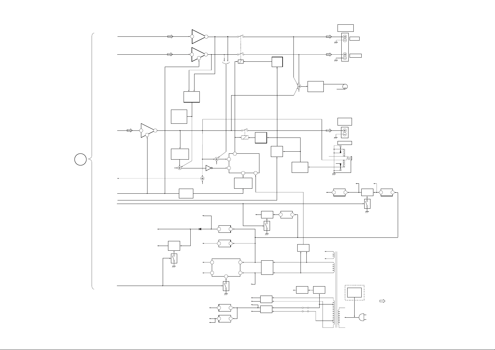
Page 23
Page 24
Page 25
Page 26
Page 27
Page 28

Page 29

Page 30

Page 31

Page 32

Page 33

Page 34

Page 35

Page 36

7-19. IC BLOCK DIAGRAMS
• BD section
IC101 CXD2545Q
FSTO
XTAI
XTAO
XTSL
VCKI
PLL
OVERSAMPLING
A/D
16
TES214TEST17TES3
)
MUX
TIMING
GENERATOR 1
SUBCODE
P-W
PROCESSOR
SUBCODE
Q
PROCESSOR
18-TIMES
FILTER
21
AVDD40AVDD
VPCO
EFM
DEMODULATOR
SYNC
PROTECTOR
PROCESSOR
MIRR
DFCT
FOK DETECTOR
23
AVSS35AVSS
F
R
BUFF
RRFF
RESISTER
ERROR CORRECTOR
CLV
GENERATOR 2
SERVO
MICRO PROGRAM
INTERFACE
SERVO DSP PWM GENERATOR
SLED SERVO
TRACKING
SERVO
FOCUS SERVO
41
15
ADD90ADD
DVSS65DVSS
LEVEL
SHIFT
MUTE
ADDRESS
GENERATOR
DATA PROCESSOR
TIMING
81
22
XRST
32K RAM
37
IGEN
BUFF
BUFF
BUFF
PRIORITY
ENCODER
D/A
PEAK DETECTOR
SEQUENCER
44
45
BIAS
LRCK
WDCK
28 GND
27 CH4 OUT F
26 CH4 OUT R
25 VB IN
24 VS IN
23 VB IN
22 VCC
21 VCC
20 CH3 F IN
19 CH3 R IN
18 CAPA IN 3
17 CH3 OUT R
16 CH3 OUT F
15 MUTE
SERIAL
PARALLEL
PROCESSOR
DIGITAL OUT
CPU INTERFACE
SERVO
AUTO
SCLK
2
2
2
2
2
2
84
85
98
99
ATSK
SSTP
LOCK
DFSW
SLED PWM
GENERATOR
TRACKING PWM
GENERATOR
FOCUS PWM
GENERATOR
66
82
83
FSTI
DIRC
IC103 CXA1821M
1
LD VCCVCC
PD LD ON
2
A LC/PD
3
B RFE
4
C RFO
5
D FE
6
VEE FE BIAS
7
VC
F TE
8
E VC
9
VC
EI EO
10
67 62 63 64 20 19
C4M
68
69C16M 43 PSSL
18PDO
13VCO1
12VCO0
33PCO
32FILI
31FILO
34CLTV
36RFAC
38ASYI
39ASYO
42ASYE
73WFCK
74SCOR
76EXCK
75SBSO
72EMPH
78SQCK
77SQSO
95MON
94FSW
96MDP
97MDS
26RFDC
27TE
28SE
29FE
3025VC
(
DOUBLE SPEED
ASYMMETRY
CORRECTION
NOISE
SHAPER
SWITCH
&
BUFFER
24
RFC
ADIO
CLOCK
GENERATOR
DIGITAL
VARI-PITCH
CONVERTER
IC102 BA6392FP
BUFF
1CH1 OUT F
BUFF
2CH1 OUT R
3CAPA IN 1
R
4CH1 R IN
INTERFACE
F
5CH1 F IN
6VREF IN
7VREF OUT
8GND
FF
9CH2 F IN
INTERFACE INTERFACE
RR
10CH2 R IN
11CAPA IN 2
BUFF BUFF
12CH2 OUT R
BUFF
13CH2 OUT F
14GND
— 73 —
16
VEE
DA01-1661-46
79 MUTE
71 D OUT
70 MD2
86 DATA
88 CLOK
87 XLAT
80 SENS
89 COUT
91 MIRR
92 DFCT
93 FOK
SFON, SFDR3, 100
SRON, SRDR1, 2
TFDR, TFON4, 7
TRON, TRDR5, 6
FFDR, FFON8, 11
FRON, FRDR9, 10
VCC
VREF
VEE
VC
RF SUMMING AMP
VEE
VC
VCC
VEE
APC LD AMP
FOCUS ERROR AMP
TRACKING ERROR AMP
VC
VC
RF EQ AMP
VC
VC BUFFER
• Video section
IC101 CXD8567AM
PLMPLM
CLOCK
GENERATOR
28
D Vdd 2
27
26
25
24
23
22
21
20
19
18
17
16
15
1INIT
SYSM L1 (+)
2
ATT A Vdd L
3
SHIFT L2 (+)
4
MODES/P
LATCH A Vss L
5
256FSO X Vss
6
TEST1 512IN
7
D Vss X OUT
8
MCKSEL X Vdd
9
XBCK A Vss R
10
DATA R2 (+)
11
LRCK A Vdd R
12
MUTE L R1 (+)
13
MUTE R D Vdd 1
14
MUTE
TIMING CIRCUIT
ATT
CIRCUIT
DC
FIR3FIR2FIR1
DITHER
AC
DITHER
SAMPLE
HOLD (X1)
3RD ORDER
NOISE SHAPER
IIR
IC201 CXD1852AQ
VDD
DCLK
B/Cb7
B/Cb6
B/Cb5
B/Cb4
B/Cb3
B/Cb2
B/Cb1
B/Cb0
G/Y7
G/Y6
G/Y5
G/Y4
G/Y3
VSS
VDD
G/Y2
G/Y1
G/Y0
R/Cr7
R/Cr6
R/Cr5
R/Cr4
R/Cr3
R/Cr2
R/Cr1
R/Cr0
XVOE
TCKI
TEST
VSS
60 VDD
59 OSDR
58 OSDG
57 OSDB
56 XOSDEN
55 MD15
54 MD0
53 MD14
52 MD1
51 MD13
50 MD2
49 MD12
48 MD3
47 MD11
46 MD4
45 VSS
44 VDD
43 MD10
42 MD5
41 MD9
40 MD6
39 MD8
38 MD7
37 XCAS0
36 XCAS2/MA9
35 XMWE
34 XRAS
33 MA8
32 MA7
31 VSS
TDI
VST
TDO
TENAI
90 89 88 87 86 85 84 83 82 81 80 79 78 77 76 75 74 73 72 71 70 69 68 67 66 65 64 63 62 61
91VSS
92HSYNC
93VSYNC
94FID/FHREF
95CBLNK/FSC
96CSYNC
97XSGRST
98CLK0O
20
19
18
17
16
15
14
13
VC
12
11
CLOCK
99DOUT
DATO
100
101
LRCO
102
BCKO
103
FSXI
104
VDD
105
VSS
106
XTL2O
CLOCK
107
XTL2I
108
VDD
109
C2PO
110
LRCI
111
DATI
112
BCKI
113
DOIN
114
XHCS
115
XHDT
116
XRW
117
XHIRQ
118
XRST
RESET
119
HA0
120
HA1
123456789101112131415161718192021222324252627282930
VSS
CLOCK
XTLOO
XTLO1
VDD
CD-ROM
DECODER
INTERFACE
HA2
HA3
HOST
HD0
HD1
HD2
VIDEO POSTPROCESSOR
SYNC GENERATOR
MPEG
AUDIO
DECODER
EACH
CIRCUIT
BLOCK
HD3
HD4
HD5
HD6
VDD
&
SYSTEM
DECODER
INTERFACE
VSS
HD7
MPEG
D-RAM
MPEG
VIDEO
DECODER
BC
MA3
VSS
MA4
MA2
MA5
MA1
MA6
MA0
— 74 —
Page 37

IC271 BU6257AFV
VSYNC
HSYNC
CHARACTER
SIZE
REGISTER
HORIZONTAL
ADDRESS
REGISTER
WRITE
ADDRESS
COUNTER
1116 15 14 13 1217181920
VB
VR
VG
BBLK
GBLK
RBLK
VC1
BLK1
CIRCUIT
PROTECT
DATA INPUT
SHIFT REGISTER
CLK
CSB
2 3 6
1
IC301 CXD1854Q
80
HORIZONTAL
SIZE
COUNTER
VERTICAL
SIZE
COUNTER
RESET
DATA
4
CBLNKO79VSYNCO78HSYNCO77VSS576BO775BO674BO573BO472BO371BO270BO169BO068VDD367Y/GO766Y/GO665Y/GO564Y/GO463Y/GO362Y/GO261Y/GO160Y/GO059VDD258C/RO757C/RO656C/RO555C/RO454C/RO353C/RO252C/RO151C/RO0
HORIZONTAL
POSITION
COUNTER
VERTICAL
ADDRESS
REGISTER
VERTICAL
POSITION
COUNTER
OSCOUT
CKOUT
VDD
5 7 8 9 10
HORIZONTAL
ADDRESS
COUNTER
VERTICAL
ADDRESS
COUNTER
OSCILLATOR
CIRCUIT
OSCIN
DATA SELECTOR
TEST CIRCUIT
TEST
CHARACTER DATA
3 BIT × 288 WORD
COLOR DATA
3 BIT × 288 WORD
VIDEO RAM
CHARACTER DATA
8 BIT × 288 WORD
CHARACTER
GENERATOR ROM
12 × 18 BIT
× 255 WORD
DISPLAY CONTROLLER
DATA REGISTER
BACKGROUND
CONTROLLER
DATA REGISTER
VSS
OUTPUT CONTROL
CSYNCO
81
82HAPGAIN0
83HAPGAIN1
84TEST
85TEN
86HAPBPF0
87IFSEL1
88HAPBPF1
89NRON
90LEVEL0
91LEVEL1
92FNR UFRZ
93XRST
94VSS7
95CSYNCI
96CBLNKI
97VSYNCI
98HSYNCI
99VDD5
100DCLKI
1
VSSO
TIMING
GENERATOR
2
BI73BI64BI55BI46BI37BI28BI19BI0
8 8 8
YUV-RGB
CONVERSION
Y
B-Y
C/R-Y
NOISE
REDUCER
C/R-Y
RGB-YUV
CONVERSION
8
10
11
VSS1
Y/GI712Y/GI613Y/GI514Y/GI415Y/GI316Y/GI217Y/GI118Y/GI0
Y
B-Y
8 8
MICRO COMPUTER
INTERFACE
D-RAM
MEMORY
CONTROLLER
19
20
VSS2
C/RI721C/RI622C/RI523C/RI424C/RI325C/RI226C/RI127C/RI0
50 VSS4
49 VCPT
48 VCP
47 HVCCT
46 HVCC
45 ADVS
44 ADVD
43 CORON
42 BLCKST3
41 VSS3
40 BLCKST2
39 BLCKST1
38 BLCKST0
37 VDD1
36 BLCKSIZE
35 BLCKNR1
34 BLCKNR0
33 SXP COM
32 SDO
31 SDI
28
29
30
XCS
XSCK
VDD0
— 75 —
Page 38

IC401 CXD1913Q
10bit
DAC
10bit
DAC
10bit
DAC
-
XTEST1
XTEST336TD835TD934VDD33TD1O
37-39
32 CO
31 AVSS3
30 AVDD3
29 YO
28 AVSS2
27 AVDD2
26 VG
25 VB
24 COMPO
23 AVSS1
22 AVDD1
21 VREF
20 IREF
XVRST50XCS49SCK48SI
51
52
F1
53VDD
54XTEST4
55XRST
56SYSCLK
57PDCLK
1/2
58VSS
59VSYNC
60HSYNC
61SO
62FID
63VDD
64XIICEN
4 4
1-4
-
Y7
Y4
3
BURST FLAG
SYNC Gen.
and
Timing Controller
SIO and I2O-Bus
Controller
Dempx,
Level
Translator
and
Interpolator
4 : 2 : 2 to
8
5
6-9
-
Y3
VSS
4 : 4 : 4
8
10
11-18
-
C7
C0
Y0
VDD
CSYNC
Sub Carrier
Gen.
Closed Caption Encoder
(for NTSC)
Y
U
V
Delay
LPF
LPF
VSS
47
SYNC Slope
Gen.
CHROMA
Modulator
19
VSS
TDO45TCK44TMS43TDI42VDD41TRST40VSS
46
TEST MODE
Y, C/
Y, U, V
selector and
Interpolator
• Main section
IC102 MC14052BCP
VDD2
1
141516 13 12 11 10 9
12 3 456 78
0
2
COMMON30
COMMON
3
1
INHIBIT
SEL.A
DECODER
EE
V
SEL.B
SS
V
IC103, 1702 MC14053BCP
1
B1
B0
C.COM
INH
VEE
VSS
2
C1
3
4
5
CO
6
7
8
OPEN
OPEN
OPEN
VDD
16
B.COM
15
14
A.COM
13
A1
A0
12
11
A
10
B
C
9
— 76 —
Page 39

IC601 LA2786
ON/OFF
CURRENT
LIMITER
START
CIRCUIT
VREF
OVER HEAT
PROTECT
ON/OFF
CURRENT
LIMITER
1
2 3
4
5 6 7 8 9 10
VCC
VMUTE VCC
VREF
ERROR
AMP
VREF
ERROR
AMP
VO1
VCC
CN1
EN
EN DISPLAY
GND
NC
CN2
VEE
VO2
~_
1.8V
~_
140uA
COMPARATER
BPF1
BPF2
VREF
S-CH DC OUT
C-CH DC OUT
L-CH DC OUT
R-CH DC OUT
VREF
L-IN
R-IN
V
L-BPF1
L-BPF2
L-BPF3
1
NOISE
FILTER
2
3
V REF
4
5
6
7
8
9
10
SS
11
12
13
14
BALANCE
CONTROL
CONTROL
VR
P. S.P. S.
NOISE
CH
VR
VR
LPF
VCAVCA
VCAVCA
VCAVCA
VCAVCA
LPF
LPF
+
GENERATOR
DIVIDER
CMODE
NOISE
MUTE
+
OSC
CTRIM
CONTROL
CLK
42
41
DATA
ENABLE
40
OSC1
39
38
V
CC
L-OUT
37
R-OUT
36
S-OUT
35
34
C-OUT
CMODE-CAP.
33
C-TRIM DC CUT
32
R-BPF1
31
R-BPF2
30
R-BPF3
29
DC CUT
DC CUT
R RECT
L RECT
VLR-TH
VLR-1
VLR-2
V
SS
OUT
INL-CH
A-GND
NC
CS1
GND
CK
15
16
17
18
19
20
21
IC604 TC9210P
1
2
3
4
5
6
7
8
LEVEL
SHIFT
CIRCUIT
L-CH
DATA
LATCH
CIRCUIT
RECT RECT RECT RECT
LOG
DIFF
SHIFT RESISTER
(13bit)
STROBE OSC
CIRCUIT
CIRCUIT
R-CH
DATA
LATCH
DUAL T
LEVEL
SHIFT
CIRCUIT
CONTROL
LOG
DIFF
28
DC CUT
27
DC CUT
L-R RECT
26
25
L+R RECT
VCS-TH
24
VCS-1
23
VCS-2
22
IC901 LA5617
16
V
DD
OUT
15
14
IN
R-CH
13
A-GND
12
NC
11
CS2
STB
10
9
DATA
— 77 —
Page 40

IC602 LV1016
OSC
A.GND
VDD
OSC
22
2324
20 19 18 17 16 15 14 13
21
DC-CUT
L-OUT
R-OUT
VREF
S-OUT
A
B
DEC
2 3
CLK
DATA
4
ENABLE
1
D.GND
• Deck section
IC402 LB1641
VDD
IN-FILTER
(40kHz)
5 6
NR-DET
ADM-CONT SRAM
7
VCC
NR-IREF
A
B
ADM
A
B
+
L+DELAY
B
A
–
L–R
+
L+R
(–6dB)
A
B
8
L-IN
A
9 10 12
R-IN
OUT-FILTER
(7k/5k)
B-NR
B
S-IN
A
+
R+DELAY
B
DC-OUT
INV-PHASE
A
B
11
DELAY-OUT
VOL/MUTE
S-TRIM
DC-CUT
IC602 uPC1330HA
T.S.D O.C.P
MOTOR
DRIVE
FWD/REV/STOP
CONTROL LOGIC
2 3
1
GND
DRIVE
MOTOR
NOISE
FILTER
5 6 7 8 9 10
4
VCC 1
FWD.IN
REV.IN
CLAMP
VCC 2
• Panel section
IC761 M65850P
1
LPF1IN
VCC
1/2 VCC
AUTO
RESET
LPF1
CLOCK
REF
OP2IN
OP2OUT
LPF2IN
OSCILLATOR
CLOCK
RESET
CONTROL
D1
2 345 6 7
OP1OUT
LPF1OUT
MAIN
A/D
DO0
OP1IN
DO1
CC1
D/A
MO
LPF2
20KBIT
SRAM
MI
CC2
LPF2OUT
891014 13 12 11
GND
NOISE
FILTER
MOTOR
DRIVE
DRIVE
MOTOR
• Power section
IC301 uPC1237HA
1 2 3
2
1
SW R1 GND SW P1
OVER LOAD DET
OFFSET DET
LATCH/
AUTORESET
INVERTER
COMPARATER
GND
6
5
VCC
V
MUTE
CC
7 8 9
SW P2 GND
ON
4
3
CONT
F/F
AC OFF
DET
4 5 6 7 8
SW R2
CC
V
— 78 —
Page 41

• CD motor section
IC201 TA8409S
STANDBY
BLOCK
HEAT
CUT OFF
BLOCK
2 3
1
VCC OUT2 NC GND
IN2
• KEY CON section
IC1401 M65847FP
VREF
BLOCK
5 6
4
7
VS
OUT1 VREF IN1
8
9
MODE2
MODE1
DAIINTOUT
27
D/A
2
DA1CONT
26
3
DA2CONT
28
1
ADCONT
IC1403 MC14053BCP
1
B1
B0
2
C1
3
C.COM
4
5
CO
6
INH
7
VEE
8
VSS
DAIINTIN
ADINTOUT
25
24
A/D
RESET RAM
4 5
KEY UP
KEY DOWN
OPEN
OPEN
OPEN
LPF1IN
ADINTIN
22
23
–
+
LPF1
REF REF REF REF
LOGIC
6
7
CLKO/KEY0
SDATA/KEY1
16
15
14
13
12
11
10
9
LPF1OUT
HPFIN
HPFOUT
21
8
SCK/KEY2
VDD
B.COM
A.COM
A1
A0
A
B
C
19
20
–
+
HPF LPF2 MIX
CLOCK
GENERATOR
10
9
KEY4
STROBE/KEY3
11
LPF2IN
18
–
+
KEY5
LPF2OUT
17
REF
12
REF
13
MIXIN
16
–
+
GND
MIXOUT
15
14
VCC
— 79 —
Page 42

7-20. IC PIN FUNCTIONS
• IC101 DIGITAL SIGNAL PROCESSOR (CXD2545Q)/BD board
Pin No.
1
2
3
4
5
6
7
8
9
10
11
12
13
14
15
16
17
18
19
20
21
22
23
24
25
26
27
28
29
30
31
32
33
34
35
36
37
38
39
40
41
42
43
44
45
46
47
48
49
50
Pin Name
SRON
SRDR
SFON
TFDR
TRON
TRDR
TFON
FFDR
FRON
FRDR
FFON
VCOO
VCOI
TEST
DV
SS
TES2
TES3
PDO
VPCO
VCKI
AVD2
IGEN
AVS2
ADIO
RFC
RFDC
TE
SE
FE
VC
FILO
FILI
PCO
CLTV
AVS1
RFAC
BIAS
ASYI
ASYO
AVD1
DD
DV
ASYE
PSSL
WDCK
LRCK
DATA
BCLK
64DATA
64BCLK
64LRCK
I/O
Sled drive output (Not used)
O
Sled drive output
O
Sled drive output (Not used)
O
Tracking drive output
O
Tracking drive output (Not used)
O
Tracking drive output
O
Tracking drive output (Not used)
O
Focus drive output
O
Focus drive output (Not used)
O
Focus drive output
O
Focus drive output (Not used)
O
VCO output for analog EFM (Eight to Fourteen Modulation) PLL (Not used)
O
VCO input from analog EFM (Eight to Fourteen Modulation) PLL (Ground)
I
TEST pin connected normally to ground
I
Digital ground
–
TEST pin connected normally to ground
I
TEST pin connected normally to ground
I
Charge-pump output for analog EFM (Eight to Fourteen Modulation) PLL (Not used)
O
Charge-pump output for variable pitch PLL (Not used)
O
Clock input from variable pitch external VCO (Ground)
I
Analog power supply
–
Power supply pin for operational amplifiers
I
Analog ground
–
(Not used)
I
(Not used)
O
RF signal input
I
Tracking error signal input
I
Sled error signal input
I
Focus error signal input
I
Center voltage input pin
I
Filter output for master PLL
O
Filter input for master PLL
I
Charge-pump output for master PLL
O
Control voltage input for master VCO
I
Analog ground
–
EFM (Eight to Fourteen Modulation) signal input
I
Asymmetry circuit constant current input
I
Asymmetry comparate voltage input
I
EFM (Eight to Fourteen Modulation) full swing output
O
Analog power supply
–
Digital power supply
–
Asymmetry circuit ON/OFF
I
Audio data output mode selection input
I
48-bit slot D/A interface. word clock.
O
48-bit slot D/A interface. LR clock.
O
DA 16 output when PSSL=1. 48-bit slot serial data when PSSL=0
O
DA 15 output when PSSL=1. 48-bit slot data when PSSL=0
O
DA 14 output when PSSL=1. 64-bit slot data when PSSL=0 (Not used)
O
DA 13 output when PSSL=1. 64-bit slot data when PSSL=0 (Not used)
O
DA 12 output when PSSL=1. 64-bit slot data when PSSL=0 (Not used)
O
— 80 —
Function
Page 43

Pin No.
51
52
53
54
55
56
57
58
59
60
61
62
63
64
65
66
67
68
69
70
71
72
73
74
75
76
77
78
79
80
81
82
83
84
85
86
87
88
89
90
91
92
93
94
95
96
97
98
99
100
GTOP
XUGF
XPLCK
GFS
PFCK
C2PO
XRAOF
MNT3
MNT2
MNT1
MNT0
XTAI
XTAO
XTSL
SS
DV
FSTI
FSTO
FSOF
C16M
MD2
DOUT
EMPH
WFCK
SCOR
SBSO
EXCK
SUBQ
SQCK
MUTE
SENS
XRST
DIRC
SCLK
DFSW
ATSK
DA TA
XLAT
CLOK
COUT
DD
DV
MIRR
DFCT
FOK
FSW
MON
NDP
MDS
LOCK
SSTP
SFDR
Pin Name
I/O
DA 11 output when PSSL=1. GTOP output when PSSL=0 (Not used)
O
DA 10 output when PSSL=1. XUGF output when PSSL=0 (Not used)
O
DA 09 output when PSSL=1. XPLCK output when PSSL=0
O
DA 08 output when PSSL=1. GFS output when PSSL=0
O
DA 07 output when PSSL=1. RFCK output when PSSL=0
O
DA 06 output when PSSL=1. C2PO output when PSSL=0 (Not used)
O
DA 05 output when PSSL=1. XRA0F output when PSSL=0
O
DA 04 output when PSSL=1. MNT3 output when PSSL=0
O
DA 03 output when PSSL=1. MNT2 output when PSSL=0
O
DA 02 output when PSSL=1. MNT1 output when PSSL=0
O
DA 01 output when PSSL=1. MNT0 output when PSSL=0
O
X’tal oscillator circuit input
I
X’tal oscillator circuit output (Not used)
O
X’tal selection input pin (Ground)
I
Digital ground
–
2/3 divider input of pins 62, 63
I
2/3 divider output of pins 62, 63
O
(Not used)
O
16.9344 MHz output (Not used)
O
Digital-out ON/OFF control pin (+5V)
I
Digital-out output pin
O
Playback disc output in emphasis mode (Not used)
O
WFCK (Write Frame Clock) output
O
Sub-code sync output
O
Sub-P through Sub-W serial output (Not used)
O
Clock input for SBSO read-out (Ground)
I
Sub-Q 80-bit output
O
Clock input for SQSO read-out
I
Muting selection pin
I
SENS output
O
System reset
I
Used in 1-track jump mode (+5V)
I
SENS serial data read-out clock
I
Defect selection pin (Ground)
I
Input pin for anti-shock (Ground)
I
Serial data input, supplied from CPU
I
Latch input, supplied from CPU
I
Serial data transfer clock input, supplied from CPU
I
Numbers of track counted signal output (Not used)
O
Digital power supply
–
Mirror signal output
O
Defect signal output
O
Focus OK output
O
Output to select spindle motor output filter (Not used)
O
Output to control ON/OFF of spindle motor (Not used)
O
Output to control spindle motor servo
O
Output to control spindle motor servo (Not used)
O
GFS (Guarded Frame Sync) is sampled by 460 Hz.
O
H when GFS (Guarded Frame Sync) is H (Not used)
Input signal to detect disc inner most track
I
Sled drive output
O
Function
— 81 —
Page 44

• IC201 MPEG DECODER (CXD1852AQ)/VIDEO board
Pin No.
1
2
3
4
5
6
7
8
9
10
11
12
13
14
15
16
17
18
19
20
21
22
23
24
25
26
27
28
29
30
31
32
33
34
35
36
37
38
39
40
VSS
XTL0O
XTL0I
V
DD
HA2
HA3
HD0
HD1
HD2
HD3
HD4
HD5
HD6
DD
V
VSS
HD7
MA3
MA4
MA2
MA5
MA1
SS
V
MA6
MA0
BC
TCKI
TDI
TENAI
TDO
VST
SS
V
MA7
MA8
XRAS
XMWE
XCAS2
/MA9
XCAS0
MD7
MD8
MD6
Pin Name
I/O
–
Ground
Video decoder master clock pin. Input the XTL0I clock or connect an oscillator between
O
XTL0I and XTL0O. The recommended frequencies are 27MHz, 28.6363MHz (NTSC
I
8fsc), and 35.4686 MHz (PAL 8fsc).
–
+5V power supply
I
Address input pin. In some cases, serves as the control signal and data input according to
I
the setting of the control mode.
Function
I/O
I/O
I/O
I/O
Data input/output
I/O
I/O
I/O
–
+5V power supply
–
Ground
I/O
Data input/output
O
O
O
Address signal pin. Connect to the DRAM address pin with the same number.
O
O
–
Ground
O
Address signal pin. Connect to the DRAM address pin with the same number.
O
I
I
I
For test (Not used)
I
I
I
For test (Connect to ground)
–
Ground
O
Address signal pin. Connect to the DRAM address pin with the same number.
O
RAS signal pin. Connect to the RAS pin of the DRAM. Same for the 256Kw × 16b,
O
256Kw × 16b × 2, and 512Kw × 8b × 2 DRAM structures.
O
WE signal pin. Connect to the WE pin of the DRAM.
CAS signal. Connect to the CAS pin of the DRAM so as to control the lower bytes of the
O
upper word (256K to 512K-1) for the 256Kw × 16b × 2 DRAM structure. / Address signal
pin. Connect to the DRAM address pin with the same number. (Not used)
CAS signal. Connect to the CAS pin of the DRAM so as to control the lower bytes (MD0
O
to MD7) for 256Kw × 16b and 512Kw × 8b × 2 DRAM structures, and to control the
lower bytes of the lower word (0 to 256K-1) for the 256Kw × 16b × 2 DRAM structure.
I/O
Data input/output signal pin. Connect to the DRAM data pin so that the lower and upper
I/O
bytes of the data correspond to the CAS0 to CAS3 controls.
I/O
— 82 —
Page 45

Pin No.
41
42
43
44
45
46
47
48
49
50
51
52
53
54
55
56
57
58
59
60
61
62
63
64
65
66
67
68
69
70
71
72
73
74
75
76
77
78
79
80
Pin Name
MD9
MD5
MD10
DD
V
VSS
MD4
MD11
MD3
MD12
MD2
MD13
MD1
MD14
MD0
MD15
XOSDEN
OSDB
OSDG
OSDR
DD
V
VSS
XVOE
R/Cr0
R/Cr1
R/Cr2
R/Cr3
R/Cr4
R/Cr5
R/Cr6
R/Cr7
G/Y0
G/Y1
G/Y2
DD
V
VSS
G/Y3
G/Y4
G/Y5
G/Y6
G/Y7
I/O
I/O
Data input/output signal pin. Connect to the DRAM data pin so that the lower and upper
I/O
bytes of the data correspond to the CAS0 to CAS3 controls.
I/O
–
+5V power supply
–
Ground
Function
I/O
I/O
I/O
I/O
I/O
Data input/output signal pin. Connect to the DRAM data pin so that the lower and upper
I/O
bytes of the data correspond to the CAS0 to CAS3 controls.
I/O
I/O
I/O
I/O
I
OSD enable signal
I
OSD data input pin. When the XOSDEN input is “L”, the color registered in the register
I
specified by this 3 inputs (3 bits) is output as the image data.
I
–
+5V power supply
–
Ground
Video output enable signal pin. When set to “L”, enables the image data output and DCLK
I
output. When set to “H”, disables (high impedance). Output control can also be performed
by writing in the register. (Connected to ground)
O
O
O
O
Output pin of the R or Cr signal of the image data. MSB is R/Cr7. Synchronizes with
O
DCLK.
O
O
O
O
Output pin of the G or Y signal of the image data. MSB is G/Y7. Synchronizes with
O
DCLK.
O
–
+5V power supply
–
Ground
O
O
Output pin of the G or Y signal of the image data. MSB is G/Y7. Synchronizes with
O
DCLK.
O
O
— 83 —
Page 46

Pin No.
81
82
83
84
85
86
87
88
89
90
91
92
93
94
95
96
97
98
99
100
101
102
103
104
105
Pin Name
B/Cb0
B/Cb1
B/Cb2
B/Cb3
B/Cb4
B/Cb5
B/Cb6
B/Cb7
DCLK
DD
V
VSS
HSYNC
VSYNC
FID
/FHREF
CBLNK
/FSC
CSYNC
XSGRST
CLK0O
DOUT
DATO
LRCO
BCKO
FSXI
DD
V
VSS
I/O
Function
O
O
O
Output pin of the B or Cb signal of the image data. MSB is B/Cb7. Synchronizes with
O
DCLK. (Not used)
O
O
O
O
Dot clock (DCLK) signal pin. The DCLK frequency is normally 13.5MHz. The DCLK can
be input from this pin or can be made by frequency-dividing (1/integer) the clock input
I
from XTL0I.
+5V power supply
–
Ground
–
Horizontal sync signal pin. When using the built-in sync generator, a signal is made by
frequency-dividing the dot clock (DCLK). Serves as the input when not using the built-in
I
sync generator.
Ver tical sync signal pin. When using the built-in sync generator, a signal is made by fre-
I
quency-dividing the DCLK. Serves as the input when not using the b uilt-in sync generator .
Field determination signal. Odd field correspond to “H” and even field correspond to “L”.
Serves as an output when the built-in sync generator is used, and as an input when not.
/ Signal obtained by frequency-dividing the clock input from XTL0I or XTLI. When the
I
input clock is 8 fsc, it can be used as the horizontal sync signal phase comparison reference
signal.
Composite blanking signal pin. Serves as an output when the built-in sync generator is
used, and as an input when not. / Signal obtained by frequency-dividing the clock input
I
from XTL0I or XTLI. When the input clock is 8 fsc, it can be used as the fsc signal.
Composite sync signal pin. A signal is made by frequenc y-dividing the DCLK. Cannot be
O
input. (Not used)
Sync generator reset signal pin. The signal generator is initialized by setting this pin to “L”.
I
Outputs the frequency-divided clock of the clock input to XTL0I. The frequency dividing
O
ratio can be selected from 1/2, 1/4, and 1/8. (Not used)
Digital output (Not used)
O
Audio serial data output to Audio D/A converter (IC101)
O
LR clock output to Audio D/A converter (IC101)
O
Bit clock output to Audio D/A converter (IC101)
O
Input 384fs (16.9344MHz) or 768fs (33.8688MHz).
I
+5V power supply
–
Ground
–
106
107
108
109
110
XTL2O
XTL2I
V
DD
C2PO
LRCI
CD-ROM decoder , audio decoder master clock. Input a clock to the XTL21 or connect an
O
oscillator between XTL2I and XTL2O. The recommended frequency is 45 MHz. This
clock is for the internal circuit. Does not synchronize with inputs and outputs.
I
+5V power supply
–
C2 pointer input (CXD2545Q)
I
LR clock input (CXD2545Q)
I
— 84 —
Page 47

Pin No.
111
112
113
114
115
116
117
118
119
120
Pin Name I/O Function
DATI
BCKI
DOIN
XHCS
XHDT
HRW
XHIRQ
XRST
HA0
HA1
Serial data input (CXD2545Q)
I
Bit clock input (CXD2545Q)
I
Digital input signal (Not used)
I
Register access chip select signal pin.
I
Data acknowledge/wait signal pin for DMA transmission, register access, transparent
I/O
memory access.
Register access control signal pin.
I
Interrupt request signal
O
Hardware reset input pin. When set to “L”, all register s and operations are reset and initialized.
I
Address input pin. In some cases, serves as the control signal and data input according to
I
the setting of the control mode.
I
— 85 —
Page 48

• IC301 NOISE REDUCTION (CXD1854Q)/VIDEO board
Pin No.
1
2
3
4
5
6
7
8
9
10
11
12
13
14
15
16
17
18
19
20
21
22
23
24
25
26
27
28
29
30
31
32
33
34
35
36
37
38
39
40
41
42
43
44
45
46
47
48
49
50
Pin Name
SS
V
BI7
BI6
BI5
BI4
BI3
BI2
BI1
BI0
SS
V
Y/GI7
Y/GI6
Y/GI5
Y/GI4
Y/GI3
Y/GI2
Y/GI1
Y/GI0
SS
V
C/RI7
C/RI6
C/RI5
C/RI4
C/RI3
C/RI2
C/RI1
C/RI0
DD
V
XCS
XSCK
SDI
SDO
SXP COM
BLCKNR0
BLCKNR1
BLCKSIZE
DD
V
BLCKST0
BLCKST1
BLCKST2
SS
V
BLOCKST3
CORON
ADVD
ADVS
HVCC
HVCCT
VCP
VCPT
SS
V
I/O
Ground
–
[MSB]
I
I
I
I
B input 0–7 (Connect to ground)
I
I
I
I
[LSB]
Ground
–
[MSB]
I
I
I
I
G (Y) input 0–7
I
I
I
[LSB]
I
Ground
–
[MSB]
I
I
I
I
R (Cb/Cr) input 0–7
I
I
I
[LSB]
I
–
Power supply (+5V)
Chip select input from IIC interface (IC901)
I
Serial clock input from IIC interface (IC901)
I
Serial data input from IIC interface (IC901)
I
Serial data output. (Not used)
O
Serial/parallel select
I
NR effect level control input
I
NR effect level control input
I
Block size select input
I
–
Power supply (+5V)
RAS signal for DRAM (Connected to ground)
I
CAS signal for DRAM (Connected to ground)
I
Write enable signal for DRAM (Connected to ground)
I
Ground
–
I
DRAM data input (Connected to ground)
DRAM data input (Connected to +5V)
I
DRAM data input (Connected to +5V)
I
DRAM data input (Connected to ground)
I
DRAM data input (Not used)
I
DRAM data input (Connected to +5V)
I
DRAM data input (Not used)
I
DRAM data input (Connected to ground)
I
Ground
–
Function
— 86 —
Page 49

Pin No.
51
52
53
54
55
56
57
58
59
60
61
62
63
64
65
66
67
68
69
70
71
72
73
74
75
76
77
78
79
80
81
82
83
84
85
86
87
88
89
90
91
92
93
94
95
96
97
98
99
100
Pin Name
C/RO0
C/RO1
C/RO2
C/RO3
C/RO4
C/RO5
C/RO6
C/RO7
DD
V
Y/GO7
Y/GO6
Y/GO5
Y/GO4
Y/GO3
Y/GO2
Y/GO1
Y/GO0
DD
V
BO0
BO1
BO2
BO3
BO4
BO5
BO6
BO7
SS
V
HSYO
VSYO
CBLO
CSYO
HAPGAIN0
HAPGAIN1
TEST
TEN
HAPBPF0
IFSEL 1
HAPBPF1
NRON
LEVEL 0
LEVEL 1
FNR UFRZ
XRST
SS
V
CSYI
CBLI
VSYI
HSYI
DD
V
DCLKI
I/O
O
[MSB]
Function
O
O
O
R (Cb/Cr) output 0–7
O
O
O
[LSB]
O
Power supply (+5V)
–
[MSB]
O
O
O
O
G (Y) output 0–7
O
O
O
[LSB]
O
Power supply (+5V)
–
[MSB]
O
O
O
O
B output 0–7 (Not used)
O
O
O
[LSB]
O
Ground
–
H SYNC output (Not used)
O
V SYNC output (Not used)
O
Composit blanking output (Not used)
O
Composit SYNC output (Not used)
O
Profile cooperation effect level control
I
Profile cooperation effect level control
I
Test pin (Connect to ground)
I
Test pin (Connect to +5V)
I
Profile cooperation correction band control
I
Matrix select Y/C, RGB (Connect to ground)
I
Profile cooperation correction band control
I
Noise reducer on/off (L: off, H: on)
I
Noise reducer level select
I
0: weak –3: strong (Not used)
I
NR feedback coefficient deser processor select (Connect to +5V)
I
Power on reset
I
Ground
–
Composit SYNC input (Connect to ground)
I
Composit blanking input (Connect to +5V)
I
V SYNC input
I
H SYNC input
I
Power supply (+5V)
–
Dot clock input (13.5MHz)
I
— 87 —
Page 50

• IC401 10 BIT VIDEO D/A CONVERTER (CXD1913Q)/VIDEO board
Pin No.
1
2
3
4
5
6
7
8
9
10
11
12
13
14
15
16
17
18
19
20
21
22
23
24
25
26
27
28
29
30
31
32
33
34
Y7
Y6
Y5
Y4
V
SS
Y3
Y2
Y1
Y0
DD
V
C7
C6
C5
C4
C3
C2
C1
C0
SS
V
IREF
VREF
DD1
AV
SS1
AV
COMPO
VB
VG
DD2
AV
SS2
AV
YOUT
AV
DD3
SS3
AV
COUT
TD10
V
DD
Pin Name
I/O
I
8-bit pixel data input pins (PD0 to 7).
I
When control register bit “PIF MODE”=“0”, serve as input pins for multiplexed Y, Cb,
I
Cr signals.
I
When control register bit “PIF MODE”=“1”, serve as input pins for Y signal
–
Digital ground
I
8-bit pixel data input pins (PD0 to 7).
I
When control register bit “PIF MODE”=“0”, serve as input pins for multiplexed Y, Cb,
I
Cr signals.
I
When control register bit “PIF MODE”=“1”, serve as input pins for Y signal
–
Digital power supply
Function
I
I
8-bit pixel data input pins/test data bus.
I
When control register bit “PIF MODE”=“0”, these input pins cannot be used.
I
When control register bit “PIF MODE”=“1”, serve as input pins for multiplexed Cb, Cr
I
signals.
I
In the test mode, used for internal circuit test data bus.
I
The test mode is allowed to use only for device vendors
I
–
Digital ground
Reference current output pin.
O
Connect a resistor ×16 times (“16R”) of the output resistance value “R”
Voltage reference input pin.
I
Sets the output full-scale value
–
Analog power supply
–
Analog ground
10-bit D/A converter output.
O
When control register bit “YC/YUV”=“1”, outputs the composite signal.
When control register bit “YC/YUV”=“0”, outputs the color difference (V) signal
I
Connect to Vss with an approx. 0.1 µF capacitor
I
Connect to AV
Analog power supply
–
Analog ground
–
10 bit D/A converter output.
O
(Luminance (Y) signal output.)
Analog power supply
–
Analog ground
–
DD with an approx. 0.1 µF capacitor
10-bit D/A converter output.
When control register bit “YC/YUV”=“1”, outputs the chroma (C) signal.
O
When control register bit “YC/YUV”=“0”, outputs the color difference (U) signal
Test data bus.
In the test mode, used for internal circuit test data bus.
O
The test mode is allowed to use only for device vendors (Not used)
Digital power supply
–
— 88 —
Page 51

Pin No.
Pin Name
I/O
Function
35
36
37
38
39
40
41
42
43
44
45
46
47
48
49
50
51
52
53
54
55
56
TD9
TD8
XTEST1
XTEST2
XTEST3
SS
V
TRST
DD
V
TDI
TMS
TCK
TDO
SS
V
SI
SCK
XCS
XVRST
F1
V
DD
XTEST4
XRST
SYSCLK
O
Test data bus.
In the test mode, used for internal circuit test data bus.
O
The test mode is allowed to use only for device vendors (Not used)
I
Test mode control input pin. Pulled-up.
I
When these pins are “H”, CXD1913Q is not in the test mode.
I
The test mode is allowed to use only for device vendors
–
Digital ground
Test mode reset input pin.
I
During power on/reset, set to “L” for more than 40 clocks (SYSCLK) (Not used)
–
Digital power supply
I
Test mode control input pin. (Not used)
I
I
Test mode control input pin. Fix at “H”
O
Test data bus pin. (Not used)
–
Digital ground
The functions of this pin are selected by Pin 64 XIICEN.
When the XIICEN pin is “H”, sets into the SONY SIO mode, and becomes the SI serial
I
data input pin.
When the XIICEN pin is “L”, sets into the I
2
C-BUS mode, and becomes the SDA input/
output pin
The functions of this pin are selected by Pin 64 XIICEN.
When the XIICEN pin is “H”, sets into the SONY SIO mode, and becomes the SCK serial
I
clock input pin.
2
When the XIICEN pin is “L”, sets into the I
C-BUS mode, and becomes the SCL input pin
The functions of this pin are selected by Pin 64 XIICEN. Pulled-up.
When the XIICEN pin is “H”, sets into the SONY SIO mode, and becomes the XCK chip
I
select input pin.
2
When the XIICEN pin is “L”, sets into the I
address selection input signal which selects the I
C-BUS mode, and becomes the SA slave
2
C-BUS slave address
Active “L” vertical sync reset input pin. Pulled-up.
I
Used for synchronizing external vertical sync and internal vertical sync.
When XVRST is “L”, the internal digital sync generator is reset according to the F1 state
Field ID input pin.
When externally synchronizing with the XVRST signal, the field to be reset is determined
I
by this signal.
“H” indicates the first field.
“L” indicates the second field
–
Digital power supply
Test mode control input pin. Pulled-up.
I
When these pins are “H”, CXD1913Q is not s test mode.
The test mode is allowed to use only for device vendors
System reset input pin when active “L”.
I
During power on/reset, set to “L” for more than 40 clocks (SYSCLK)
System clock input pin.
I
To generate the correct sub carrier frequency, precisely 27MHz is required
— 89 —
Page 52

Pin No.
57
58
59
60
61
62
63
64
PDCLK
SS
V
VSYNC
HSYNC
SO
FID
V
DD
XIICEN
Pin Name
I/O
Function
13.5MHz pixel data clock output pin.
This clock is obtained by 1/2 frequency-dividing SYSCLK.
O
Used only in the 16-bit pixel data mode
Digital ground
–
V.sync signal output
O
H.sync signal output
O
The functions of this pin are selected by Pin 64 XIICEN.
When the XIICEN pin is “H”, sets into the SONY SIO mode, and becomes the S0 serial-
O
out output pin.
When the XIICEN pin is “L”, this pin is not used and sets into high impedance (Not used)
Field ID output.
When control register bit “FDS”=“1”, “L” indicates the first field and “H” indicates the
second field.
O
When control register bit “FDS”=“0”, “H” indicates the first field and “L” indicates the
second field
Digital power supply
–
Serial interface mode selection input pin. Pulled-up.
2
When “L”, Pins 48 to 50, and 61 set into the I
I
C-BUS mode.
When “H”, Pins 48 to 50, and 61 set into the SONY SOP mode
— 90 —
Page 53

• IC701 MECHANISM CONTROL (HD6433032SK12F)/VIDEO board
Pin No.
1
2
3
4
5
6
7
8
9
10
11
12
13 to 20
21
22 to 29
30
31 to 35
36 to 39
40, 41
42
43
44
45
46
47
48
49
50
51
52
53
54
55
56
57
58
59
60
61
62
63
64
65
66
67
Pin Name
CMD0
CMD1
CMD2
CMD3
SACK
QINT
VDAC-XLAT
DF-XLAT
P90/TXD
SUBQ
SQCK
SS
V
D0 to D7
CC
V
A0 to A7
V
SS
A8 to A12
A13 to A16
A17, A18
A19
W AIT
MD0
MD1
φ
STBY
RESET
NM1
SS
V
EXT AL
XT AL
V
CC
AS
RD
WR
RESO
SS
AV
TEST0
TEST1
TE
SENS
DAC-SELECT
NPIN
VSS
VREQ
VREF
I/O
Input/output terminal exchanging data bus 0 with IIC interface (IC901)
I/O
Input/output terminal exchanging data bus 1 with IIC interface (IC901)
I/O
Input/output terminal exchanging data bus 2 with IIC interface (IC901)
I/O
Input/output terminal exchanging data bus 3 with IIC interface (IC901)
I/O
Outputs command acknowledge to IIC interface (IC901)
O
Outputs command output pulses to IIC interface (IC901)
O
Serial data latch pulse output to Video D/A converter (IC401)
O
Serial data latch pulse output to Audio D/A converter (IC101)
O
Not used
–
Sub Q 80bit input (CXD2545Q)
I
SQSO readout clock output (CXD2545Q)
O
Ground
–
Data bus input/output (IC201, 751)
I/O
Connect to the power supply (+5V)
–
Address bus output (IC201, 751)
O
Ground
–
Address bus output (IC201, 751)
O
Address bus output (Not used)
O
Addres bus output (IC772)
O
Address bus output (Not used)
O
BUS control wait input (IC201)
I
Operation mode setting terminal (Connected to +5V)
I
Operation mode setting terminal (Connected to ground)
I
System clock output (Not used)
O
Shifts to the hardware standby mode when the standby terminal becomes “Low”.
I
(Unable to use H level fixed) (Connected to +5V)
Set into reset when the reset input pin becomes “Low”. (IC901)
I
Requests mask disable interruption. (Unable to use H level fixed) (Connected to +5V)
I
Ground
–
Connected to the Crystal oscillator. The EXTAL pin is also able to input external clocks.
I
(10 MHz)
Connected to the Crystal oscillator. (10 MHz)
I
Power supply (+5V)
–
When the address strobe pin is “Low”, indicates that address outputs on the address bus
O
are valid. (IC772)
When the read pin is “Low”, indicates that the external addresses space is in the read state.
O
(IC201, 751)
When the read pin is “Low”, indicates that the external addresses space is in the write
O
state and the data bus are valid. (IC201, 751)
Reset output (Not used)
O
A/D converter (Pin62-69) ground
–
Color-bar test input (“L” = test)
I
AFADJ test input (“L” = test)
I
ADJ test input (“L” = test)
I
Internal state (SENSE) monitor input (CXD2545Q)
I
Audio D/A converter select mode setting terminal (Connected to +5V)
I
NTSC/PAL output mode setting terminal (0V : NTSC, 1.5V : AUTO, 3V : PAL)
I
Ground
–
Not used
I
A/D converter (Pin62-69) reference voltage input (Connected to +5V)
I
Function
— 91 —
Page 54

Pin No.
68
69
70
71
72
73
74
75
76
77
78
79
80
Pin Name
CC
AV
CHECK-LED
XHIRQ
SCOR
MREQ
DATA
AMUTE
LDON
XLT
SCLK
CLK
NR-SEL
—
I/O
A/D converter (Pin62-29) power supply (Connected to +5V)
–
Check LED control (Error : flashing)
O
Interruption request input from MPEG decoder
I
Subcode sync input (CXD2545Q)
I
Inputs command request from IIC interface (IC901)
I
Serial data output
O
Mute output (“H” = mute)
O
Laser diode ON/OFF output
O
Latch output (CXD2545Q)
O
SENS serial data reading clock output (CXD2545Q)
O
Serial data clock output
O
Connected to +5V
I
Not used
–
Function
— 92 —
Page 55

• IC901 IIC INTERFACE (uPD780016YGF-012-3BA)/VIDEO board
Pin No.
1 to 8
9
10
11
12
13
14
15
16, 17
18
19 to 22
23
24
25 to 32
33
34
35
36
37
38, 39
40
41, 42
43
44
45
46
47
48
49
50
51
52
53
54
55
56
57 to 64
65
66
67
68
69, 70
71
72, 73
74 to 81
82 to 85
86 to 93
94 to 100
Pin Name
P80 to P87
TEST
X2
X1
VDD
XT2
XT1
RESET
PO0, PO1
QINT
PO3 to PO6
VDD
AVDD
P10 to P17
AVSS
CMD0
CMD1
CMD2
CMD3
P24, P25
VSS
P26, P27
MREQ
SACK
CDGM
P93
MDATA
MCLK
OS-XLAT
G-XLAT
G-XRST
CD-XRST
CDPOW
DOUT
IIC-DATA
IIC-CLK
P40 to P47
NRON
LEVEL0
LEVEL1
NR-XCS
P54, P55
VSS
P56, P57
P60 to P67
P100 to P103
P30 to P37
P150 to P156
I/O Function
Connected to ground
I
Connected to ground
–
X’ tall (5MHz)
O
X’ tall (5MHz)
I
Power supply +5V
–
Not used
–
Connected to +5V
–
System reset input
I
Not used (Fixed at “L”)
I
CD-BUS interrupt input
I
Not used (Fixed at “L”)
I
Power supply +5V
–
Power supply +5V
–
Connected to ground
I
Ground
–
Input/output terminal exchanging data bus 0 with mecha-con, (IC901)
I/O
Input/output terminal exchanging data bus 1 with mecha-con, (IC901)
I/O
Input/output terminal exchanging data bus 2 with mecha-con, (IC901)
I/O
Input/output terminal exchanging data bus 3 with mecha-con, (IC901)
I/O
Connected to ground
I
Ground
–
Connected to ground
I
Output command request to mecha-con. (IC701)
O
Input command acknowledge from mecha-con. (IC701)
I
Not used (Fixed at “L”)
I
Connected to ground
I
Serial data output (IC271, 301)
O
Serial clock output (IC271, 301)
O
Serial latch output to OSD (IC271)
O
Not used
O
Not used
O
Video CD section reset output
O
Not used
O
Not used
O
Serial data input from master control (IC701)
I
Serial clock input from master control (IC701)
I
Connected to ground
I
Not used
O
Not used
O
Not used
O
Chip select output to noise reduction (IC301)
O
Connected to ground
I
Ground
I
Connected to ground
I
Connected to ground
I
Connected to ground
I
Connected to ground
I
Connected to ground
I
— 93 —
Page 56

• IC701 MASTER CONTROL (uPD780016YGF-019-3BA)/MAIN board
Pin No.
1 TA-MUTE O Line mute signal outputA
2 DBFB-H/L O DBFB H/L select signal output
3 427-LT O Latch signal output for IC201 (62427)
4 KCON-LT O Latch signal output for key control
5
6 F-RELAY O Front speaker relay control output (Not used)
7 R-RELAY O Rear speaker relay control output
8 PL-RELAY O Not used
9 TEST I Connected to ground
10 X2 O
11 X1 I
12 VDD – Power supply (+5V)
13 XT2 O
14 XT1 I
15 RESET I Reset signal input
16 INT/IN I
17 INT/IN/OUT I
18 SCOR O Subcode data request signal output (Connected to ground)
19 SOFT-TEST O Software test port
20 AC-CUT I Back up signal input
21 RDS-INT I Not used
22 RDS-DATA I Not used
23 VDD – Power supply (+5V)
24 AVDD I Analog reference voltage input.
25 ADJ I CD adjust point port Normal “H”
26 A-SHUT I A Deck reel pulse detector
27 B-SHUT I B Deck reel pulse detector
28 B-HALF I Half detector signal input
29 CLK-CHECK I Connected to ground
30 SPEC-IN I Version select signal input
31 ADJ 2 I Connected to ground
32 DEMO-CHANGE I DEMO H/L select signal input (Fixed at fixed at “L”)
33 AVSS – Ground
34 SQ-DATA-IN I Subcode Q data clock input (Not used)
35 — I Not used
36 SQ-CLK I Sub code Q data clock input (Not used)
37 SW-ON/OFF O Not used
38, 39 FUNC 1, 2 I Connected to ground
40 VSS – Ground
41 VOL-LAT O Latch signal to erectrial volume (IC604)
42 PL-LAT O Latch signal to pro-logic (IC601, 602)
43 COM-DIN I Connected to ground
44 COM-DOUT O Common serial data output
45 COM-CLK O Common serial clock output
46 CD-POWER O CD power on signal output
47 CD-DATA O CD data output (Not used)
48 CD-CLK O CD clock output (Not used)
49 MSM-CMD O Not used
50 MSM-BUSY I Connected to ground
Pin Name I/O Function
KCON-ON
O Key contr ol ON/OFF signal output
X’tal (5MHz)
X’tal (32.768 KHz)
Connected to ground
— 94 —
Page 57

Pin No.
51 MSM-LT O
52 MSM-NAR I Not used
53 MSM-CH O
54 INPUT-CHANGE O Input sensitivity switching output
55 IIC-DATA O Data output for IC601, 901
56 IIC-CLK O Clock output for IC601, 901
57 XRST O CD reset signal output
58 XLT O CD latch signal output (Not used)
59 FOUCUS-SW O Not used
60 TBL-L O
61 TBL-R O
62 TRAY-LED O CD tray LED ON/OFF output
63 LOAD-OUT O
64 LOAD-IN O
65 ST-CLK O Tuner clock output
66 ST-DIN I Tuner data input
67 ST-DOUT O Tuner data output
68 ST-CE O Tuner chip enable output
69 TUNED I Tuned detection for tuner
70 STEREO I Stereo detection for tuner
71 VSS – Ground
72 ST-MUTE O Tuner mute signal output
73 SENS2 I
74 SENS I
75 DISC-SENS I Not used
76 T-SENS I CD table detection signal input
77 UP-SW I Up SW (S201) signal input
78 ENC 3 I
79 ENC 2 I Not used
80 ENC 1 I
81 OUT-OPEN I Not used
82 CAP-M-H/N O Capstan motor H/N speed select signal output
83 B-TRG O Trigger motor control output
84 A-TRG O Trigger motor control output
85 TRG-LOW O Trigger motor control output
86 CAP-M-ON/OFF O Capstan motor ON/OFF signal output
87 PB-A/B O PB Deck A/Deck B select output
88 EQ-H/N O Equalizer H/N select output
89 BIAS O Bias ON/OFF signal output
90 REC-MUTE O REC mute ON/OFF selection output
91 NR-ON/OFF O NR ON/OFF signal output
92 R/P-PASS O REC/PB/PASS selection output
93 TC-MUTE O TC mute ON/OFF selection output
94 A-PLAY-SW I Deck A play detect
95 B-PLAY-SW I Deck B play detect
96 TC-RELAY O REC/PB head selection output for IC602
97 A-HALF I Deck A cassette detect
98 POWER O POWER ON/OFF signal output
99 SW-F-CHG O Super woofer mode signal output
100 STK-MUTE O Power amp ON/OFF signal output
Pin Name I/O Function
Table motor control output
Not used
BD Condition signal input (Not used)
— 95 —
Page 58

• IC601 DISPLAY CONTROL (TMP87CM75-6565)/PANEL board
Pin No.
1 SEG35 O FL segment signal output
2 VLOAD O Power supply (–25V) for FL segment signal output
3 to 10 LED1 to LED8 O LED driver output
11 VSS – Ground
12 X-OUT O
13 X-IN I
14 RESET I Reset signal input from main controller
15 LED 9 O
16 LED10 O Connected ground
17 TEST I
18 to 23 LED11 to LED16 O LED driver output
24 VOL-A I Rotary encoder (S701) pulse input
25 LED17 O LED driver output
26 JOG-A I Rotaly encoder (S711) pulse input
27 CLOCK I Serial clock input from main controller
28 DATA I Serial data input from main controller
29 LED SELECT O LED select signal output
30 VDD – Power supply (+5V)
31 VSS – Ground
32 MODEL I Version select signal input
33 to 37 KEY1 to KEY5 I Key input
38 DOOR SW I DOOR SW (S691) ON/OFF signal input
39 SIRCS I Remote commander signal input
40 VOL-B I Rotary encoder (S701) pulse input
41 JOG-B I Rotary encoder (S711) pulse input
42 SPEANA-1 I Spectrum analyzer input
43 SPEANA-2 I Spectrum analyzer input
44 SPEANA-3 I Spectrum analyzer input
45 SPEANA-4 I Spectrum analyzer input
46 L + R I Spectrum analyzer (high frequency) input
47 LED18 O LED driver output
48 VASS – Ground
49 VAREF I Analog reference voltage input
50 VDD – Power supply (+5V)
51 to 56 GR1 to GR16 O FL gride signal output
67 to 100 SEG1 to SEG34 O FL segment signal output
Pin Name I/O Function
X’tall (8MHz)
• Abbreviation
FL : Fluorescent indicator tube
— 96 —
Page 59

SECTION 8
EXPLODED VIEWS
NOTE:
• Items marked “*” are not stocked since they are
seldom required for routine service. Some delay
should be anticipated when ordering these items.
• The mechanical parts with no reference number in
the exploded views are not supplied.
• Hardware (# mark) list and accessories and packing materials are given in the last of this parts list.
8-1. CASE AND BACK PANEL SECTION
2
4
1
4
• Abbreviation
SP : Singapore model
MY : Malaysia model
IA : Indonesia model
CH : Chinese model
#2
#2
1
#2
The components identified by mark !
or dotted line with mark ! are critical
for safety.
Replace only with part number
specified.
3
#1
#3
#1`
#1
#1
FRONT PANEL
#1
Ref. No. Part No. Description Remark
1 4-929-973-01 SCREW (CASE, 3 POINT)
* 2 4-987-052-31 CASE
* 3 4-992-220-01 PANEL, BACK (E,SP)
* 3 4-992-220-11 PANEL, BACK (MY)
* 3 4-992-220-21 PANEL, BACK (CH)
#1
6
M901
Ref. No. Part No. Description Remark
* 3 4-992-220-31 PANEL, BACK (IA)
4 3-363-099-01 SCREW (CASE 3 TP2)
5 1-233-545-11 ENCAPSULATED COMPONENT
6 1-769-974-11 WIRE (FLAT TYPE)(13 CORE)
M901 1-698-792-11 FAN, DC
5
— 97 —
Page 60

8-2. FRONT PANEL SECTION 1
55
not supplied
73
57
TCM-220WR2
56
57
58
59
57
60
#1
57
61
57
62
not supplied
77
62
63
54
not supplied
not supplied
57
78
53
52
51
57
65
70
Supplied
with S711
57
71
72
57
66
73
64
not supplied
67
69
75
76
62
57
57
not supplied
68
74
Ref. No. Part No. Description Remark Ref. No. Part No. Description Remark
51 4-987-995-01 SPRINAG (CD EJECT), COMPRESSION
52 4-987-001-01 BUTTON (EJECT CD)
* 53 1-664-019-11 CD-A SW BOARD
54 X-4948-663-1 PANEL (A) SUB ASSY
* 55 1-664-012-11 TC-A SW BOARD
56 4-986-999-01 BUTTON (EJECT A)
57 4-951-620-01 SCREW (2.6X8), +BVTP
58 1-773-163-11 WIRE (FLAT TYPE)(21 CORE)
59 1-769-949-11 WIRE (FLAT TYPE)(11 CORE)
60 3-354-963-01 DAMPER
* 61 1-664-017-11 CD-LED BOARD
62 4-957-577-01 SCREW PTP WH (2.6X8)(DIA. 10)
* 63 1-664-016-11 DOOR SW BOARD
64 4-987-038-21 LID, DISC
* 65 4-987-933-01 BRACKET (TA)
66 4-987-000-01 BUTTON (EJECT B)
* 67 1-664-013-11 TC-B SW BOARD
* 68 1-664-020-11 CD-B1 SW BOARD
69 X-4947-969-1 BUTTON (CD STOP) ASSY
70 4-987-037-01 KNOB (JOG)
71 X-4948-296-1 PANEL (B) SUB ASSY
* 72 1-664-021-11 CD-B2 SW BOARD
73 3-568-749-00 CUSHION, ECM
74 4-987-002-01 BUTTON (CD PLAY)
75 4-987-014-01 INDICATOR (CD)
76 4-987-997-01 SPRING (CD, LID), TORSION
77 4-987-998-01 SPRING (LOCK SHAFT), TORSION
78 X-4948-664-1 BUTTON (LOOP) ASSY
— 98 —
Page 61

8-3. FRONT PANEL SECTION 2
Supplied
with RV760, RV761
not supplied
110
111
110
119
130
Supplied with J760
106
105
104
Supplied
with S701
102
108
128
109
107
103
113
112
114
129
131
126
not supplied
126
FL601
117
118
122
not supplied
115
110
116
125
110
121
124
132
120
123
101
Ref. No. Part No. Description Remark Ref. No. Part No. Description Remark
101 X-4948-662-1 PANEL ASSY
102 4-987-036-01 KNOB (VOL)
103 X-4947-961-1 LID ASSY, CASSETTE
104 4-987-032-01 DISPLAY (TA)
105 4-987-028-01 DISPLAY (ST)
106 4-987-021-01 INDICATOR (TC A)
107 4-986-997-01 BUTTON (DECK.A)
108 4-963-404-21 EMBLEM (5-A), SONY
109 4-973-644-01 KNOB (MIC)
110 4-951-620-01 SCREW (2.6X8), +BVTP
* 111 A-4392-486-A HP/MIC BOARD, COMPLETE
112 4-986-986-01 BUTTON (POWER)
113 4-987-012-01 INDICATOR (TA)
114 X-4947-990-1 BUTTON (SOUND) ASSY
115 4-986-990-01 BUTTON (CURSOR)
116 4-978-683-01 SPRING, COMPRESSION
* 117 4-987-041-01 COVER, CURSOR
127
118 X-4947-963-1 BUTTON (FUNCTION) ASSY
* 119 A-4398-986-A PANEL BOARD, COMPLETE
120 1-773-051-11 WIRE (FLAT TYPE)(17 CORE)
121 X-4947-962-1 BUTTON (TUNER) ASSY
122 4-987-013-01 INDICATOR (TUNER)
123 X-4947-968-1 BUTTON (WOOFER) ASSY
124 X-4947-967-1 BUTTON (DECK B) ASSY
125 4-987-022-01 INDICATOR (TC B)
126 4-987-996-01 SPRING (TC LID), TENSION
127 4-948-236-01 CUSHION (107)
128 4-987-930-01 PLATE (VOL), ORNAMENTAL
129 4-988-219-01 BUTTON (DOLBY)
* 130 4-986-870-11 HOLDER, FL TUBE
131 4-987-017-01 INDICATOR (KEY.CON)
* 132 4-949-935-81 CUSHION (FL)
FL601 1-517-617-11 INDICATOR TUBE, FLUORESCENT
— 99 —
Page 62

8-4. CHASSIS SECTION
162
#1
not supplied
T501
(CH)
167 166
not supplied
#1
160
#1
#2
#1
151
153
#2
#1
#4
154
#1
165
#4
#1
#1
158
not supplied
155
#1
#1
159
CNP901
(IA, CH)
CNP901
(E, SP, MY)
161
(E, SP, MY)
161
(IA)
CDM37L-5BD21AL
#1
A
156
#1
156
152
#1
164
not supplied
157
#1
not supplied
Ref. No. Part No. Description Remark Ref. No. Part No. Description Remark
* 151 1-663-994-11 TRANS BOARD
* 152 A-4398-049-A KEY CON BOARD, COMPLETE
153 3-703-244-00 BUSHING (FBS001), CORD (E,SP,MY,CH)
153 4-966-266-01 BUSHING (S)(FBS002), CORD (IA)
* 154 A-4392-679-A POWER BOARD, COMPLETE (E,SP,MY,IA)
* 154 A-4403-679-A POWER BOARD, COMPLETE (CH)
* 155 A-4398-990-A MAIN BOARD, COMPLETE
156 1-782-563-11 WIRE (FLAT TYPE)(29 CORE)
157 X-4941-228-1 FOOT (F22125H-M)
* 158 A-4392-662-A SURROUND BOARD, COMPLETE (E,SP,MY,IA)
* 158 A-4392-663-A SURROUND BOARD, COMPLETE (CH)
* 159 1-782-562-11 WIRE (FLAT TYPE)(13 CORE)
* 160 4-988-533-11 HOLDER, PCB
163
165
! 161 1-569-007-11 ADAPTOR, CONVERSION 2P (IA)
! 161 1-569-008-11 ADAPTOR, CONVERSION 2P (E,SP,MY)
* 162 1-666-126-11 VIDEO POWER BOARD
* 163 1-665-406-11 VIDEO OUT BOARD
* 164 A-4398-587-A VIDEO BOARD, COMPLETE
165 4-944-316-01 HOLDER, PC BOARD
166 1-500-386-11 FERRITE CORE (CH)
* 167 3-703-150-11 WIRE CLAMP (CH)
! CNP901 1-558-943-41 CORD, POWER (IA)
! CNP901 1-575-651-21 CORD, POWER (E,SP,MY)
! CNP901 1-782-510-11 CORD, POWER (CH)
! T501 1-431-418-11 TRANSFORMER, POWER
The components identified by mark !
or dotted line with mark ! are critical
for safety.
Replace only with part number specified.
— 100 —
Page 63

8-5. TC MECHANISM SECTION-1 (TCM-220WR2)
207
201
208
205
#5
209
203
#5
#5
206
205
207
202
not supplied
204
#2
Ref. No. Part No. Description Remark Ref. No. Part No. Description Remark
201 X-4947-943-1 HOLDER (L) ASSY, CASSETTE
202 X-4947-944-1 HOLDER (R) ASSY, CASSETTE
203 4-959-231-11 SPRING (L), TORSION
204 4-959-232-11 SPRING (R), TORSION
205 3-354-963-01 DAMPER
* 206 4-980-439-01 FULCLUM, HOLDER
207 3-354-957-01 JOINT (LOCK LEVER)
208 3-354-953-01 LEVER (LOCK LEVER L)
209 3-354-954-01 LEVER (LOCK LEVER R)
— 101 —
Page 64

8-6. TC MECHANISM SECTION-2 (TCM-220WR2)
B
not supplied
256
255
254
not supplied
HP101
(including
257
259
r
A)
253
264
262
274
258
260
not supplied
HRPE101
(including
255
not supplied
261
256
265
r
275
266
263
B)
272
273
274
267
not supplied
268
259
269
257
r
264
A
265
262
271
(including pA)
266
269
274
274
263
261
273
r
B
#6
269
r
A
#6
r
251
252
Ref. No. Part No. Description Remark Ref. No. Part No. Description Remark
251 3-908-560-01 SPRING, AZIMUTH ADJUSTMENT
252 3-919-684-01 SCREW, AZIMUTH ADJUSTMENT
253 X-3373-113-1 SLIDER (HEAD) ASSY
254 3-009-956-01 SPRING, HEAD TOGGLE
255 3-908-558-02 FITTING BLOCK, HEAD
256 3-908-557-02 ROTARY BLOCK, HEAD
* 257 3-908-559-01 STOPPER, AZIMUTH
258 3-908-555-01 SLIDER (REV SLIDER)
259 3-917-143-11 SPRING, TENSION
260 3-388-848-01 SCREW (P2X6)(B TIGHT)
261 3-939-371-01 SPRING (1), TENSION
262 X-3369-909-1 PINCH LEVER (REV) ASSY
263 X-3369-908-1 PINCH LEVER (FWD) ASSY
264 3-908-613-01 GEAR (S), REEL
#9
not supplied
252
251
#9
254
not supplied
260
258
253
265 3-917-141-01 SPRING, COMPRESSION
266 X-3371-305-1 REEL (T) ASSY
267 3-669-465-01 WASHER (1.5), STOPPER
268 X-3370-173-1 TU ASSY
269 3-939-862-01 CLIP
* 271 A-2007-131-A AUDIO BOARD, COMPLETE
272 3-930-972-01 DETENT, HALF
273 3-917-142-01 SPRING, COMPRESSION
274 3-355-808-02 PINCH ROLLER
275 3-938-863-01 STOPPER
HP101 1-500-093-11 HEAD, MAGNETIC (PLAYBACK)
HRPE1011-500-094-11 HEAD, MAGNETIC (REC/PB/ERASE)
— 102 —
Page 65

8-7. TC MECHANISM SECTION-3 (TCM-220WR2)
0
pA: MOTOR board (Suppplied with AUDIO board)
313
302
317
309
318
316
#9
315
319
320
324
A
p
310
311
M2
323
310
308
305
321
#11
321
#10
#1
325
306
307
312
319
304
#8
322
307
314
314
303
#7
#7
M1
Ref. No. Part No. Description Remark Ref. No. Part No. Description Remark
301 3-908-597-01 CAM (A)
302 3-908-608-11 SCREW, STEP
303 X-3372-930-3 ARM (A) ASSY, FR
304 X-3370-169-1 FLYWHEEL (AR) ASSY
305 3-928-047-01 PULLEY, TENSION
306 3-908-599-01 LEVER (REV-A)
307 3-908-601-01 SPRING (REV LEVER), TORSION
308 3-908-603-01 LEVER (TRIGGER A)
309 X-3367-593-1 FLYWHEEL (BF) ASSY
310 3-908-605-01 SPRING (TRIGGER), TORSION
311 3-908-609-01 GEAR, TRIGGER
312 3-913-845-11 BELT (A)
313 3-913-846-11 BELT (FR)
314 X-3370-171-1 FLYWHEEL (BR) ASSY
not supplied
315 3-908-600-01 LEVER (REV-B)
* 316 1-650-669-11 LEAF SWITCH BOARD
317 3-908-598-01 CAM (B)
318 X-3372-931-3 ARM (B) ASSY, FR
319 3-911-114-12 SPRING (FR), TORSION
320 3-908-604-01 LEVER (TRIGGER B)
321 3-911-115-01 WASHER, STOPPER
322 3-917-176-11 BELT (B)
323 X-3370-172-1 FLYWHEEL (AF) ASSY
* 324 A-2007-131-A AUDIO BOARD, COMPLETE
325 X-3371-441-1 CHASSIS ASSY, MECHANICAL
M1 X-3371-223-1 MOTOR ASSY (CAPSTAN)
M2 A-2004-410-A MOTOR ASSY (TRIGGER)
302
301
— 103 —
Page 66

8-8. CD MECHANISM SECTION (CDM37L-5BD21AL)
353
352
351
362
not
supplied
354
360
M201
352
360
363
351
355
356
367
357
359
365
#1
#1
358
368
361
361
368
372
369
373
374
351
360
375
368
369
370
#1
#1
Ref. No. Part No. Description Remark Ref. No. Part No. Description Remark
351 4-987-976-01 SCREW, STEP
352 4-944-490-01 BELT (TIMING)
353 A-4660-978-A GEAR (PULLEY) ASSY
354 4-978-421-01 GEAR (MID)
355 4-978-425-01 ROLLER (CAM)
356 4-978-420-01 CAM (HOLDER)
* 357 1-452-925-11 MAGNET ASSY
358 4-978-417-01 TABLE, DISC
359 4-993-142-01 PULLEY (L), PRESS
360 X-4947-960-1 ROLLER ASSY
* 361 4-978-583-01 BRACKET (BU)
* 362 4-978-418-01 CHASSIS
* 363 4-980-385-01 HOLDER (SW)
* 364 A-4673-765-A CD MOTOR BOARD, COMPLETE
#1
364
366
371
365 4-978-426-01 INDICATOR (NO.)
* 366 1-659-059-13 LED BOARD
* 367 1-659-058-13 TABLE SENSOR BOARD
368 4-933-134-01 SCREW (+PTPWH M2.6X6)
369 4-958-593-01 SPRING (BU), COMPRESSION
* 370 4-978-419-01 HOLDER (BU-5)
371 4-917-583-71 BRACKET, YOKE
372 4-989-493-01 SLIDER (37)
373 4-989-494-01 SCREW (SLIDER), STEP
374 4-989-819-01 SPRING, TENSION
375 4-989-491-21 COVER, LENS
M201 A-4660-977-A MOTOR ASSY (TABLE)
— 104 —
Page 67

8-9. BASE UNIT SECTION (BU-5BD21AL)
401
402
#12
403
405
404
M101
M102
408
404
406
407
The components identified by mark !
or dotted line with mark ! are critical
for safety.
Replace only with part number specified.
Ref. No. Part No. Description Remark Ref. No. Part No. Description Remark
! 401 8-820-020-03 OPTICAL PICK-UP KSS-213D/Q-NP
402 1-769-069-11 WIRE (FLAT TYPE)(16 CORE)
403 4-917-567-01 GEAR (M)
404 4-951-940-01 INSULATOR (BU)
405 4-917-565-01 SHAFT, SLED
406 4-917-564-01 GEAR (P), FLATNESS
* 407 A-4673-557-A BD BOARD, COMPLETE
408 4-951-620-01 SCREW (2.6X8), +BVTP
M101 X-4917-523-4 MOTOR ASSY (SPINDLE)
M102 X-4917-504-1 MOTOR ASSY (SLED)
— 105 —
Page 68

AUDIO
Note:
The components identified by mark !
or dotted line with mark ! are critical
for safety.
Replace only with part number specified.
When indicating parts by reference
number, please include the board
name.
Ref. No. Part No. Description Remark Ref. No. Part No. Description Remark
* A-2007-131-A AUDIO BOARD, COMPLETE
*********************
< CAPACITOR >
ELECTRICAL PARTS LIST
• Due to standardization, replacements in the parts list
may be different from the parts specified in the
diagrams or the components used on the set.
• -XX, -X mean standardized parts, so they may have
some difference from the original one.
• Items marked “*” are not stocked since they are
seldom required for routine service. Some delay
should be anticipated when ordering these items.
• RESISTORS
All resistors are in ohms
MET AL: Metal-film resistor
MET AL OXIDE: Metal Oxide-film resistor
F : nonflammable
(including MOTOR board)
CN601 1-695-382-31 PIN, CONNECTOR (PC BOARD) 21P
CN602 1-564-718-11 PIN, CONNECTOR (SMALL TYPE) 2P
* CN651 1-564-521-11 PLUG, CONNECTOR 6P
• SEMICONDUCTORS
In each case, u: µ , for example:
uA...: µ A..., uPA...: µ PA..., uPB...: µ PB...,
uPC...: µ PC..., uPD...: µ PD...
• CAPACITORS
uF : µ F
• COILS
uH : µ H
• Abbreviation
SP : Singapore model
MY : Malaysia model
IA : Indonesia model
CH : Chinese model
< CONNECTOR >
SECTION 9
C301 1-162-289-31 CERAMIC 390PF 10% 50V
C302 1-126-968-11 ELECT 100uF 20% 6.3V
C303 1-162-282-31 CERAMIC 100PF 10% 50V
C304 1-130-483-00 MYLAR 0.01uF 5% 50V
C305 1-107-715-11 ELECT 22uF 20% 16V
C311 1-162-289-31 CERAMIC 390PF 10% 50V
C313 1-162-282-31 CERAMIC 100PF 10% 50V
C314 1-130-487-00 MYLAR 0.022uF 5% 50V
C315 1-126-233-11 ELECT 22uF 20% 50V
C331 1-137-427-11 FILM 120PF 5% 50V
C332 1-162-288-31 CERAMIC 330PF 10% 50V
C333 1-162-209-31 CERAMIC 27PF 5% 50V
C401 1-162-289-31 CERAMIC 390PF 10% 50V
C402 1-126-968-11 ELECT 100uF 20% 6.3V
C403 1-162-282-31 CERAMIC 100PF 10% 50V
C404 1-130-483-00 MYLAR 0.01uF 5% 50V
C405 1-107-715-11 ELECT 22uF 20% 16V
C411 1-162-289-31 CERAMIC 390PF 10% 50V
C413 1-162-282-31 CERAMIC 100PF 10% 50V
C414 1-130-487-00 MYLAR 0.022uF 5% 50V
C415 1-126-233-11 ELECT 22uF 20% 50V
C431 1-137-427-11 FILM 120PF 5% 50V
C432 1-162-288-31 CERAMIC 330PF 10% 50V
C433 1-162-209-31 CERAMIC 27PF 5% 50V
C601 1-104-396-11 ELECT 10uF 20% 16V
< IC >
IC601 8-759-111-44 IC uPC4570C-1
IC602 8-759-143-54 IC uPC1330HA
IC611 8-759-111-44 IC uPC4570C-1
< COIL >
L331 1-410-780-11 INDUCTOR 27mH
L431 1-410-780-11 INDUCTOR 27mH
< MOTOR >
M2 A-2004-410-A MOTOR ASSY (TRIGGER)
< TRANSISTOR >
Q621 8-729-142-46 TRANSISTOR 2SC2001-LK
Q622 8-729-142-46 TRANSISTOR 2SC2001-LK
Q623 8-729-801-93 TRANSISTOR 2SD1387
Q651 8-729-900-65 TRANSISTOR DTA144ES
< RESISTOR >
R301 1-247-881-00 CARBON 120K 5% 1/4W
R302 1-249-409-11 CARBON 220 5% 1/4W F
R303 1-249-433-11 CARBON 22K 5% 1/4W
R304 1-247-889-00 CARBON 270K 5% 1/4W
R305 1-247-858-11 CARBON 13K 5% 1/4W
C602 1-104-396-11 ELECT 10uF 20% 16V
C611 1-124-907-11 ELECT 10uF 20% 50V
C612 1-124-907-11 ELECT 10uF 20% 50V
C621 1-137-150-11 FILM 0.01uF 5% 100V
C622 1-126-961-11 ELECT 2.2uF 20% 50V
C623 1-136-155-00 FILM 0.015uF 5% 50V
C624 1-130-481-00 MYLAR 0.0068uF 5% 50V
C625 1-130-481-00 MYLAR 0.0068uF 5% 50V
C627 1-124-903-11 ELECT 1uF 20% 50V
C628 1-136-153-00 FILM 0.01uF 5% 50V
C642 1-104-664-11 ELECT 47uF 20% 16V
C651 1-161-494-00 CERAMIC 0.022uF 25V
R311 1-247-881-00 CARBON 120K 5% 1/4W
R312 1-247-807-31 CARBON 100 5% 1/4W
R314 1-247-882-11 CARBON 130K 5% 1/4W
R315 1-247-850-11 CARBON 6.2K 5% 1/4W
R331 1-249-430-11 CARBON 12K 5% 1/4W
R401 1-247-881-00 CARBON 120K 5% 1/4W
R402 1-249-409-11 CARBON 220 5% 1/4W F
R403 1-249-433-11 CARBON 22K 5% 1/4W
R404 1-247-889-00 CARBON 270K 5% 1/4W
R405 1-247-858-11 CARBON 13K 5% 1/4W
R411 1-247-881-00 CARBON 120K 5% 1/4W
R412 1-247-807-31 CARBON 100 5% 1/4W
R414 1-247-882-11 CARBON 130K 5% 1/4W
R415 1-247-850-11 CARBON 6.2K 5% 1/4W
R431 1-249-430-11 CARBON 12K 5% 1/4W
— 106 —
Page 69

AUDIO
Ref. No. Part No. Description Remark Ref. No. Part No. Description Remark
R601 1-249-409-11 CARBON 220 5% 1/4W F
R602 1-249-409-11 CARBON 220 5% 1/4W F
R608 1-249-409-11 CARBON 220 5% 1/4W F
R609 1-249-433-11 CARBON 22K 5% 1/4W
R611 1-249-409-11 CARBON 220 5% 1/4W F
R612 1-249-409-11 CARBON 220 5% 1/4W F
! R621 1-212-851-00 FUSIBLE 5.6 5% 1/4W F
! R622 1-212-851-00 FUSIBLE 5.6 5% 1/4W F
R623 1-249-432-11 CARBON 18K 5% 1/4W
R624 1-249-432-11 CARBON 18K 5% 1/4W
C156 1-163-237-11 CERAMIC CHIP 27PF 5% 50V
C157 1-163-145-00 CERAMIC CHIP 0.0015uF 5% 50V
C159 1-163-019-00 CERAMIC CHIP 0.0068uF 10% 50V
C161 1-163-038-91 CERAMIC CHIP 0.1uF 25V
< CONNECTOR >
CN101 1-774-115-11 CONNECTOR, (FFC/FPC) 29P
CN102 1-770-014-11 CONNECTOR, FFC/FPC 16P
< IC >
BD
R625 1-249-429-11 CARBON 10K 5% 1/4W
R651 1-247-856-00 CARBON 11K 5% 1/4W
R652 1-247-856-00 CARBON 11K 5% 1/4W
R653 1-249-441-11 CARBON 100K 5% 1/4W
< VARIABLE RESISTOR >
RV301 1-238-598-11 RES, ADJ, CARBON 2.2K
RV311 1-238-598-11 RES, ADJ, CARBON 2.2K
RV341 1-238-551-11 RES, ADJ, CARBON 220K
RV401 1-238-598-11 RES, ADJ, CARBON 2.2K
RV411 1-238-598-11 RES, ADJ, CARBON 2.2K
RV441 1-238-551-11 RES, ADJ, CARBON 220K
RV651 1-238-599-11 RES, ADJ, CARBON 4.7K
RV652 1-238-599-11 RES, ADJ, CARBON 4.7K
< TRANSFORMER >
T621 1-423-980-11 TRANSFORMER, BIAS OSCILLATION
**************************************************************
* A-4673-557-A BD BOARD, COMPLETE
*******************
< CAPACITOR >
C101 1-163-005-11 CERAMIC CHIP 470PF 10% 50V
C102 1-163-038-91 CERAMIC CHIP 0.1uF 25V
C103 1-163-005-11 CERAMIC CHIP 470PF 10% 50V
C105 1-104-913-11 TANTAL. CHIP 10uF 20% 16V
C106 1-164-346-11 CERAMIC CHIP 1uF 16V
C107 1-164-346-11 CERAMIC CHIP 1uF 16V
C108 1-163-035-00 CERAMIC CHIP 0.047uF 50V
C109 1-163-145-00 CERAMIC CHIP 0.0015uF 5% 50V
C110 1-163-017-00 CERAMIC CHIP 0.0047uF 5% 50V
C111 1-163-251-11 CERAMIC CHIP 100PF 5% 50V
C112 1-163-038-91 CERAMIC CHIP 0.1uF 25V
C113 1-163-038-91 CERAMIC CHIP 0.1uF 25V
C115 1-126-607-11 ELECT CHIP 47uF 20% 4V
C116 1-126-607-11 ELECT CHIP 47uF 20% 4V
C117 1-126-209-11 ELECT 100uF 20% 4V
C118 1-163-275-11 CERAMIC CHIP 0.001uF 5% 50V
C119 1-163-235-11 CERAMIC CHIP 22PF 5% 50V
C123 1-164-232-11 CERAMIC CHIP 0.01uF 50V
C124 1-164-005-11 CERAMIC CHIP 0.47uF 25V
C125 1-104-913-11 TANTAL. CHIP 10uF 20% 16V
C140 1-163-038-91 CERAMIC CHIP 0.1uF 25V
C141 1-163-038-91 CERAMIC CHIP 0.1uF 25V
C151 1-163-237-11 CERAMIC CHIP 27PF 5% 50V
C153 1-163-038-91 CERAMIC CHIP 0.1uF 25V
C154 1-164-336-11 CERAMIC CHIP 0.33uF 25V
— 107 —
IC101 8-752-369-78 IC CXD2545Q
IC102 8-759-176-09 IC BA6392FP
IC103 8-752-072-45 IC CXA1821M-T6
< MOTOR >
M101 X-4917-523-4 MOTOR ASSY (SPINDLE)
M102 X-4917-504-1 MOTOR ASSY (SLED)
< TRANSISTOR >
Q101 8-729-010-08 TRANSISTOR MSB710-R
< RESISTOR >
R101 1-216-077-00 METAL CHIP 15K 5% 1/10W
R102 1-216-097-91 METAL GLAZE 100K 5% 1/10W
R103 1-216-077-00 METAL CHIP 15K 5% 1/10W
R104 1-216-085-00 METAL CHIP 33K 5% 1/10W
R105 1-216-097-91 METAL GLAZE 100K 5% 1/10W
R106 1-216-061-00 METAL CHIP 3.3K 5% 1/10W
R107 1-216-061-00 METAL CHIP 3.3K 5% 1/10W
R108 1-216-073-00 METAL CHIP 10K 5% 1/10W
R109 1-216-121-91 METAL GLAZE 1M 5% 1/10W
R110 1-216-025-91 METAL GLAZE 100 5% 1/10W
R112 1-216-049-91 METAL GLAZE 1K 5% 1/10W
R123 1-216-073-00 METAL CHIP 10K 5% 1/10W
R124 1-216-097-91 METAL GLAZE 100K 5% 1/10W
R125 1-216-033-00 METAL CHIP 220 5% 1/10W
R126 1-216-033-00 METAL CHIP 220 5% 1/10W
R127 1-216-033-00 METAL CHIP 220 5% 1/10W
R131 1-216-037-00 METAL CHIP 330 5% 1/10W
R132 1-216-073-00 METAL CHIP 10K 5% 1/10W
R134 1-216-049-91 METAL GLAZE 1K 5% 1/10W
R135 1-216-295-91 CONDUCTOR, CHIP (2012)
R136 1-216-295-91 CONDUCTOR, CHIP (2012)
R137 1-216-295-91 CONDUCTOR, CHIP (2012)
R138 1-216-295-91 CONDUCTOR, CHIP (2012)
R141 1-216-089-91 METAL GLAZE 47K 5% 1/10W
R142 1-216-081-00 METAL CHIP 22K 5% 1/10W
R143 1-216-103-00 METAL CHIP 180K 5% 1/10W
R144 1-216-103-00 METAL CHIP 180K 5% 1/10W
R146 1-216-073-00 METAL CHIP 10K 5% 1/10W
R147 1-216-067-00 METAL CHIP 5.6K 5% 1/10W
R148 1-216-001-00 METAL CHIP 10 5% 1/10W
R149 1-216-003-11 METAL GLAZE 12 5% 1/10W
R158 1-216-109-00 METAL CHIP 330K 5% 1/10W
R159 1-216-101-00 METAL CHIP 150K 5% 1/10W
R160 1-216-295-91 CONDUCTOR, CHIP (2012)
R161 1-216-308-00 METAL CHIP 4.7 5% 1/10W
The components identified by mark !
or dotted line with mark ! are critical
for safety.
Replace only with part number specified.
Page 70

BD CD-A SW CD-B1 SW
CD MOTORCD-LEDCD-B2 SW
Ref. No. Part No. Description Remark
R162 1-216-101-00 METAL CHIP 150K 5% 1/10W
< SWITCH >
S101 1-572-085-11 SWITCH, LEAF (LIMIT)
**************************************************************
* 1-664-019-11 CD-A SW BOARD
*************
< DIODE >
D641 8-719-058-04 DIODE SEL5223S-TP15 (CD NON-STOP)
D642 8-719-058-04 DIODE SEL5223S-TP15 (VCD)
D643 8-719-058-04 DIODE SEL5223S-TP15 (PBC)
D644 8-719-058-04 DIODE SEL5223S-TP15 (AUTO PBC)
< RESISTOR >
R731 1-249-411-11 CARBON 330 5% 1/4W
R732 1-249-413-11 CARBON 470 5% 1/4W F
R733 1-249-415-11 CARBON 680 5% 1/4W F
R734 1-249-417-11 CARBON 1K 5% 1/4W F
R735 1-249-419-11 CARBON 1.5K 5% 1/4W F
R736 1-249-421-11 CARBON 2.2K 5% 1/4W F
R737 1-249-417-11 CARBON 1K 5% 1/4W F
R738 1-249-419-11 CARBON 1.5K 5% 1/4W F
R739 1-249-421-11 CARBON 2.2K 5% 1/4W
R740 1-247-843-11 CARBON 3.3K 5% 1/4W
R741 1-247-807-31 CARBON 100 5% 1/4W
R742 1-247-807-31 CARBON 100 5% 1/4W
R743 1-247-807-31 CARBON 100 5% 1/4W
R744 1-247-807-31 CARBON 100 5% 1/4W
< SWITCH >
Ref. No. Part No. Description Remark
< RESISTOR >
R745 1-247-815-91 CARBON 220 5% 1/4W
R746 1-249-411-11 CARBON 330 5% 1/4W
R747 1-249-413-11 CARBON 470 5% 1/4W F
R748 1-249-415-11 CARBON 680 5% 1/4W F
R749 1-247-807-31 CARBON 100 5% 1/4W
R750 1-247-807-31 CARBON 100 5% 1/4W
R751 1-247-807-31 CARBON 100 5% 1/4W
< SWITCH >
S676 1-554-303-21 SWITCH, TACTILE (· SELECT)
S677 1-554-303-21 SWITCH, TACTILE (p)
S678 1-554-303-21 SWITCH, TACTILE (P)
S679 1-554-303-21 SWITCH, TACTILE (DISC SKIP)
**************************************************************
* 1-664-021-11 CD-B2 SW BOARD
**************
< RESISTOR >
R752 1-249-417-11 CARBON 1K 5% 1/4W F
R753 1-249-419-11 CARBON 1.5K 5% 1/4W F
R754 1-249-421-11 CARBON 2.2K 5% 1/4W F
R755 1-247-843-11 CARBON 3.3K 5% 1/4W
R756 1-249-427-11 CARBON 6.8K 5% 1/4W F
< SWITCH >
S681 1-554-303-21 SWITCH, TACTILE ())
S682 1-554-303-21 SWITCH, TACTILE (REPEAT)
S683 1-554-303-21 SWITCH, TACTILE (PLAY MODE)
S684 1-554-303-21 SWITCH, TACTILE (1/ALL DISCS)
S685 1-554-303-21 SWITCH, TACTILE (EDIT)
S661 1-554-303-21 SWITCH, TACTILE (DISC 1)
S662 1-554-303-21 SWITCH, TACTILE (DISC 2)
S663 1-554-303-21 SWITCH, TACTILE (DISC 3)
S664 1-554-303-21 SWITCH, TACTILE (DISC 4)
S665 1-554-303-21 SWITCH, TACTILE (DISC 5)
S666 1-554-303-21 SWITCH, TACTILE (CD FLASH)
S667 1-554-303-21 SWITCH, TACTILE (CD NON-STOP)
S668 1-554-303-21 SWITCH, TACTILE (CD LOOP)
S669 1-554-303-21 SWITCH, TACTILE (ˆ RETURN)
S670 1-554-303-21 SWITCH, TACTILE (PREV)
S671 1-554-303-21 SWITCH, TACTILE (NEXT)
**************************************************************
* 1-664-020-11 CD-B1 SW BOARD
**************
< CONNECTOR >
* CN642 1-568-943-11 PIN, CONNECTOR 5P
< DIODE >
D645 8-719-057-29 DIODE SML78423C-TP15 (· SELECT)
D646 8-719-057-97 DIODE SEL5923A-TP15 (P)
D647 8-719-057-29 DIODE SML78423C-TP15 (· SELECT)
S686 1-554-303-21 SWITCH, TACTILE (0)
S711 1-467-968-11 ENCODER, ROTARY (≠ AMS ±)
**************************************************************
* 1-664-017-11 CD-LED BOARD
************
< CONNECTOR >
CN671 1-506-481-11 PIN, CONNECTOR 2P
< DIODE >
D671 8-719-058-03 DIODE SEL5423E-TP15 (DISC TABLE)
D672 8-719-058-03 DIODE SEL5423E-TP15 (DISC TABLE)
D673 8-719-058-03 DIODE SEL5423E-TP15 (DISC TABLE)
D674 8-719-058-03 DIODE SEL5423E-TP15 (DISC TABLE)
< RESISTOR >
R791 1-249-412-11 CARBON 390 5% 1/4W F
**************************************************************
* A-4673-765-A CD MOTOR BOARD, COMPLETE
*************************
* 4-980-385-01 HOLDER (SW)
— 108 —
Page 71

CD MOTOR
Ref. No. Part No. Description Remark Ref. No. Part No. Description Remark
< CAPACITOR >
C201 1-124-907-11 ELECT 10uF 20% 50V
C202 1-164-159-21 CERAMIC 0.1uF 50V
C203 1-124-907-11 ELECT 10uF 20% 50V
< CONNECTOR >
* CN201 1-568-947-11 PIN, CONNECTOR 9P
C773 1-126-964-11 ELECT 10uF 20% 50V
C774 1-126-964-11 ELECT 10uF 20% 50V
C775 1-162-294-31 CERAMIC 0.001uF 10% 50V
C776 1-162-294-31 CERAMIC 0.001uF 10% 50V
C777 1-126-960-11 ELECT 1uF 20% 50V
C778 1-162-305-11 CERAMIC 0.0068uF 30% 16V
C779 1-162-294-31 CERAMIC 0.001uF 10% 50V
C780 1-136-495-11 FILM 0.068uF 5% 50V
DOOR SW
HP/MIC
< IC >
IC201 8-759-365-94 IC TA8409S
< COIL >
L201 1-408-117-00 INDUCTOR 10uH
< MOTOR >
M201 A-4660-977-A MOTOR ASSY (TABLE)
< RESISTOR >
R205 1-249-427-11 CARBON 6.8K 5% 1/4W F
R206 1-249-425-11 CARBON 4.7K 5% 1/4W F
< SWITCH >
S201 1-762-587-11 SWITCH, PUSH (1 KEY)(UP)
**************************************************************
* 1-664-016-11 DOOR SW BOARD
*************
< CAPACITOR >
C691 1-164-159-21 CERAMIC 0.1uF 50V
C781 1-126-957-11 ELECT 0.22uF 20% 50V
C782 1-126-957-11 ELECT 0.22uF 20% 50V
C783 1-126-967-11 ELECT 47uF 20% 10V
C784 1-136-495-11 FILM 0.068uF 5% 50V
C785 1-162-305-11 CERAMIC 0.0068uF 30% 16V
C786 1-162-294-31 CERAMIC 0.001uF 10% 50V
C787 1-124-250-11 ELECT 0.15uF 20% 50V
C788 1-126-960-11 ELECT 1uF 20% 50V
C789 1-161-494-00 CERAMIC 0.022uF 25V
C790 1-126-967-11 ELECT 47uF 20% 10V
C791 1-164-159-21 CERAMIC 0.1uF 50V
C794 1-164-159-21 CERAMIC 0.1uF 50V
C795 1-164-159-21 CERAMIC 0.1uF 50V
C798 1-164-159-21 CERAMIC 0.1uF 50V
C799 1-164-159-21 CERAMIC 0.1uF 50V
< CONNECTOR >
* CN701 1-568-935-11 PIN, CONNECTOR 8P
< DIODE >
D761 8-719-200-82 DIODE 11ES2
D762 8-719-200-82 DIODE 11ES2
D763 8-719-200-82 DIODE 11ES2
< IC >
< CONNECTOR >
CN661 1-506-481-11 PIN, CONNECTOR 2P
< SWITCH >
S691 1-771-057-11 SWITCH, PUSH (1 KEY)(6 OPEN)
**************************************************************
* A-4392-486-A HP/MIC BOARD, COMPLETE
**********************
< CAPACITOR >
C760 1-162-306-11 CERAMIC 0.01uF 20% 16V
C761 1-126-961-11 ELECT 2.2uF 20% 50V
C762 1-162-306-11 CERAMIC 0.01uF 20% 16V
C763 1-126-961-11 ELECT 2.2uF 20% 50V
C764 1-162-294-31 CERAMIC 0.001uF 10% 50V
C765 1-162-215-31 CERAMIC 47PF 5% 50V
C766 1-162-290-31 CERAMIC 470PF 10% 50V
C767 1-162-215-31 CERAMIC 47PF 5% 50V
C768 1-126-961-11 ELECT 2.2uF 20% 50V
C769 1-162-282-31 CERAMIC 100PF 10% 50V
C770 1-126-961-11 ELECT 2.2uF 20% 50V
C771 1-126-959-11 ELECT 0.47uF 20% 50V
IC760 8-759-634-51 IC M5218AP
IC761 8-759-450-96 IC M65850P
< JACK >
J760 1-770-226-41 JACK (LARGE TYPE)(PHONES)
J761 1-770-226-41 JACK (LARGE TYPE)(MIC 1)
J762 1-770-226-41 JACK (LARGE TYPE)(MIC 2)
< COIL >
L761 1-410-521-11 INDUCTOR 100uH
< BASE POST >
* LP2 1-690-880-21 LEAD (WITH CONNECTOR)
< RESISTOR >
R760 1-249-429-11 CARBON 10K 5% 1/4W
R761 1-249-417-11 CARBON 1K 5% 1/4W F
R762 1-249-429-11 CARBON 10K 5% 1/4W
R763 1-249-417-11 CARBON 1K 5% 1/4W F
R764 1-249-441-11 CARBON 100K 5% 1/4W
R765 1-249-417-11 CARBON 1K 5% 1/4W F
R766 1-249-437-11 CARBON 47K 5% 1/4W
R767 1-249-429-11 CARBON 10K 5% 1/4W
R768 1-249-431-11 CARBON 15K 5% 1/4W
— 109 —
Page 72

HP/MIC
KEY CON
LEAF SWITCH
Ref. No. Part No. Description Remark
R769 1-247-885-00 CARBON 180K 5% 1/4W
R770 1-247-807-31 CARBON 100 5% 1/4W
R771 1-247-863-91 CARBON 22K 5% 1/4W
R772 1-247-863-91 CARBON 22K 5% 1/4W
R773 1-247-863-91 CARBON 22K 5% 1/4W
R774 1-247-881-00 CARBON 120K 5% 1/4W
R775 1-247-863-91 CARBON 22K 5% 1/4W
R776 1-247-863-91 CARBON 22K 5% 1/4W
R777 1-247-863-91 CARBON 22K 5% 1/4W
R778 1-249-437-11 CARBON 47K 5% 1/4W
R779 1-249-431-11 CARBON 15K 5% 1/4W
R782 1-249-429-11 CARBON 10K 5% 1/4W
< VARIABLE RESISTOR >
RV760 1-225-366-11 RES, VAR, CARBON 50K (MIC LEVEL)
RV761 1-225-366-11 RES, VAR, CARBON 50K (ECHO LEVEL)
**************************************************************
* A-4398-049-A KEY CON BOARD, COMPLETE
************************
< CAPACITOR >
C1401 1-164-159-21 CERAMIC 0.1uF 50V
C1403 1-126-964-11 ELECT 10uF 20% 50V
C1404 1-126-964-11 ELECT 10uF 20% 50V
C1405 1-126-964-11 ELECT 10uF 20% 50V
C1406 1-126-964-11 ELECT 10uF 20% 50V
C1431 1-130-493-00 MYLAR 0.068uF 5% 50V
C1432 1-130-493-00 MYLAR 0.068uF 5% 50V
C1433 1-130-493-00 MYLAR 0.068uF 5% 50V
C1434 1-162-284-31 CERAMIC 150PF 10% 50V
C1436 1-126-967-11 ELECT 47uF 20% 10V
Ref. No. Part No. Description Remark
< TRANSISTOR >
Q1401 8-729-900-80 TRANSISTOR DTC114ES
Q1403 8-729-119-78 TRANSISTOR 2SC2785-HFE
< RESISTOR >
R1413 1-247-863-91 CARBON 22K 5% 1/4W
R1414 1-247-863-91 CARBON 22K 5% 1/4W
R1417 1-249-429-11 CARBON 10K 5% 1/4W
R1418 1-249-425-11 CARBON 4.7K 5% 1/4W F
R1419 1-249-425-11 CARBON 4.7K 5% 1/4W F
R1421 1-249-417-11 CARBON 1K 5% 1/4W F
R1422 1-249-429-11 CARBON 10K 5% 1/4W
R1431 1-247-903-00 CARBON 1M 5% 1/4W
R1435 1-247-807-31 CARBON 100 5% 1/4W
R1436 1-249-429-11 CARBON 10K 5% 1/4W
R1437 1-249-425-11 CARBON 4.7K 5% 1/4W F
R1438 1-247-807-31 CARBON 100 5% 1/4W
R1448 1-249-429-11 CARBON 10K 5% 1/4W
R1450 1-249-441-11 CARBON 100K 5% 1/4W
R1451 1-249-429-11 CARBON 10K 5% 1/4W
R1452 1-249-425-11 CARBON 4.7K 5% 1/4W F
R1453 1-249-429-11 CARBON 10K 5% 1/4W
R1457 1-249-424-11 CARBON 3.9K 5% 1/4W F
R1458 1-249-431-11 CARBON 15K 5% 1/4W
R1459 1-249-429-11 CARBON 10K 5% 1/4W
R1460 1-247-863-91 CARBON 22K 5% 1/4W
**************************************************************
* 1-650-669-11 LEAF SWITCH BOARD
*****************
< CONNECTOR >
C1437 1-164-159-21 CERAMIC 0.1uF 50V
C1438 1-126-933-11 ELECT 100uF 20% 10V
C1439 1-126-964-11 ELECT 10uF 20% 50V
C1445 1-136-165-00 FILM 0.1uF 5% 50V
C1446 1-136-165-00 FILM 0.1uF 5% 50V
C1448 1-126-964-11 ELECT 10uF 20% 50V
C1451 1-162-286-21 CERAMIC 220PF 10% 50V
C1454 1-162-286-21 CERAMIC 220PF 10% 50V
C1461 1-162-294-31 CERAMIC 0.001uF 10% 50V
C1462 1-162-306-11 CERAMIC 0.01uF 20% 16V
C1466 1-162-600-11 CERAMIC 0.0047uF 20% 16V
C1467 1-162-291-31 CERAMIC 560PF 10% 50V
C1468 1-162-290-31 CERAMIC 470PF 10% 50V
C1472 1-162-600-11 CERAMIC 0.0047uF 20% 16V
< CONNECTOR >
CN1401 1-566-999-11 PIN, CONNECTOR 13P
< IC >
IC1401 8-759-370-84 IC M65847FP-TP
IC1403 8-759-140-53 IC uPD4053BC
< COIL >
L1401 1-410-521-11 INDUCTOR 100uH
* CN1001 1-568-854-11 SOCKET, CONNECTOR 11P
< TRANSISTOR >
Q1001 8-749-010-90 TRANSISTOR PHOTO REFLECTOR
NJL5165KA-H2
Q1002 8-749-010-90 TRANSISTOR PHOTO REFLECTOR
NJL5165KA-H2
< RESISTOR >
R1001 1-247-818-11 CARBON 300 5% 1/4W
R1002 1-247-820-11 CARBON 360 5% 1/4W
R1003 1-249-414-11 CARBON 560 5% 1/4W F
R1004 1-247-834-11 CARBON 1.3K 5% 1/4W
R1005 1-247-818-11 CARBON 300 5% 1/4W
< SWITCH >
S1001 1-692-832-11 SWITCH, PUSH (1 KEY)(A PLAY)
S1002 1-692-832-11 SWITCH, PUSH (1 KEY)(B PLAY)
S1003 1-572-248-11 SWITCH, LEAF (A HALF)
S1004 1-571-281-21 SWITCH, LEAF (A CrO2)
S1005 1-571-281-21 SWITCH, LEAF (REC A)
S1006 1-572-248-11 SWITCH, LEAF (B HALF)
S1008 1-571-281-21 SWITCH, LEAF (B CrO2)
S1009 1-571-281-21 SWITCH, LEAF (REC B)
**************************************************************
— 110 —
Page 73

LED MAIN
Ref. No. Part No. Description Remark Ref. No. Part No. Description Remark
* 1-659-059-13 LED BOARD
*********
C213 1-136-171-00 FILM 0.33uF 5% 50V
C214 1-126-964-11 ELECT 10uF 20% 50V
< DIODE >
D201 8-719-032-98 DIODE SEL5820A (DISC No.)
< TRANSISTOR >
Q201 8-729-119-78 TRANSISTOR 2SC2785-HFE
< RESISTOR >
R201 1-247-863-91 CARBON 22K 5% 1/4W
R202 1-249-411-11 CARBON 330 5% 1/4W
R203 1-249-437-11 CARBON 47K 5% 1/4W
**************************************************************
* A-4398-990-A MAIN BOARD, COMPLETE
*********************
< CAPACITOR >
C101 1-162-288-31 CERAMIC 330PF 10% 50V
C103 1-162-282-31 CERAMIC 100PF 10% 50V
C104 1-162-282-31 CERAMIC 100PF 10% 50V
C105 1-126-961-11 ELECT 2.2uF 20% 50V
C106 1-130-479-00 MYLAR 0.0047uF 5% 50V
C107 1-130-473-00 MYLAR 0.0015uF 5% 50V
C108 1-136-159-00 FILM 0.033uF 5% 50V
C109 1-126-933-11 ELECT 100uF 20% 10V
C110 1-162-306-11 CERAMIC 0.01uF 20% 16V
C111 1-162-306-11 CERAMIC 0.01uF 20% 16V
C114 1-162-306-11 CERAMIC 0.01uF 20% 16V
C121 1-162-286-21 CERAMIC 220PF 10% 50V
C122 1-162-286-21 CERAMIC 220PF 10% 50V
C125 1-109-889-11 ELECT 1uF 20% 50V
C150 1-162-306-11 CERAMIC 0.01uF 20% 16V
C151 1-162-288-31 CERAMIC 330PF 10% 50V
C153 1-162-282-31 CERAMIC 100PF 10% 50V
C154 1-162-282-31 CERAMIC 100PF 10% 50V
C155 1-126-961-11 ELECT 2.2uF 20% 50V
C156 1-130-479-00 MYLAR 0.0047uF 5% 50V
C157 1-130-473-00 MYLAR 0.0015uF 5% 50V
C158 1-136-159-00 FILM 0.033uF 5% 50V
C159 1-126-933-11 ELECT 100uF 20% 10V
C164 1-162-306-11 CERAMIC 0.01uF 20% 16V
C171 1-162-286-21 CERAMIC 220PF 10% 50V
C172 1-162-286-21 CERAMIC 220PF 10% 50V
C201 1-136-167-00 FILM 0.15uF 5% 50V
C202 1-136-167-00 FILM 0.15uF 5% 50V
C203 1-136-495-11 FILM 0.068uF 5% 50V
C204 1-136-495-11 FILM 0.068uF 5% 50V
C205 1-136-156-00 FILM 0.018uF 5% 50V
C206 1-136-156-00 FILM 0.018uF 5% 50V
C207 1-130-480-00 MYLAR 0.0056uF 5% 50V
C208 1-130-479-00 MYLAR 0.0047uF 5% 50V
C209 1-130-474-00 MYLAR 0.0018uF 5% 50V
C210 1-126-964-11 ELECT 10uF 20% 50V
C211 1-126-964-11 ELECT 10uF 20% 50V
C212 1-136-171-00 FILM 0.33uF 5% 50V
C215 1-136-153-00 FILM 0.01uF 5% 50V
C230 1-136-167-00 FILM 0.15uF 5% 50V
C231 1-130-471-00 MYLAR 0.001uF 5% 50V
C234 1-126-925-11 ELECT 470uF 20% 10V
C235 1-164-159-21 CERAMIC 0.1uF 50V
C237 1-126-964-11 ELECT 10uF 20% 50V
C238 1-162-286-21 CERAMIC 220PF 10% 50V
C239 1-162-306-11 CERAMIC 0.01uF 20% 16V
C241 1-162-306-11 CERAMIC 0.01uF 20% 16V
C242 1-126-925-11 ELECT 470uF 20% 10V
C247 1-162-306-11 CERAMIC 0.01uF 20% 16V
C248 1-126-964-11 ELECT 10uF 20% 50V
C251 1-136-167-00 FILM 0.15uF 5% 50V
C252 1-136-167-00 FILM 0.15uF 5% 50V
C253 1-136-495-11 FILM 0.068uF 5% 50V
C254 1-136-495-11 FILM 0.068uF 5% 50V
C255 1-136-156-00 FILM 0.018uF 5% 50V
C256 1-136-156-00 FILM 0.018uF 5% 50V
C257 1-130-480-00 MYLAR 0.0056uF 5% 50V
C258 1-130-479-00 MYLAR 0.0047uF 5% 50V
C259 1-130-474-00 MYLAR 0.0018uF 5% 50V
C260 1-126-964-11 ELECT 10uF 20% 50V
C261 1-126-964-11 ELECT 10uF 20% 50V
C262 1-136-171-00 FILM 0.33uF 5% 50V
C263 1-136-171-00 FILM 0.33uF 5% 50V
C264 1-126-964-11 ELECT 10uF 20% 50V
C265 1-136-153-00 FILM 0.01uF 5% 50V
C275 1-162-294-31 CERAMIC 0.001uF 10% 50V
C301 1-130-479-00 MYLAR 0.0047uF 5% 50V
C302 1-162-290-31 CERAMIC 470PF 10% 50V
C303 1-130-495-00 MYLAR 0.1uF 5% 50V
C304 1-126-964-11 ELECT 10uF 20% 50V
C305 1-126-960-11 ELECT 1uF 20% 50V
C307 1-126-964-11 ELECT 10uF 20% 50V
C308 1-126-964-11 ELECT 10uF 20% 50V
C309 1-126-960-11 ELECT 1uF 20% 50V
C310 1-126-933-11 ELECT 100uF 20% 10V
C351 1-130-479-00 MYLAR 0.0047uF 5% 50V
C352 1-162-290-31 CERAMIC 470PF 10% 50V
C353 1-130-495-00 MYLAR 0.1uF 5% 50V
C355 1-126-960-11 ELECT 1uF 20% 50V
C357 1-126-964-11 ELECT 10uF 20% 50V
C358 1-126-964-11 ELECT 10uF 20% 50V
C359 1-126-960-11 ELECT 1uF 20% 50V
C360 1-126-933-11 ELECT 100uF 20% 10V
C401 1-164-159-21 CERAMIC 0.1uF 50V
C402 1-164-159-21 CERAMIC 0.1uF 50V
C403 1-164-159-21 CERAMIC 0.1uF 50V
C404 1-126-933-11 ELECT 100uF 20% 16V
C405 1-126-767-11 ELECT 1000uF 20% 16V
C601 1-136-167-00 FILM 0.15uF 5% 50V
C602 1-136-167-00 FILM 0.15uF 5% 50V
C603 1-126-962-11 ELECT 3.3uF 20% 50V
C604 1-126-962-11 ELECT 3.3uF 20% 50V
C605 1-136-167-00 FILM 0.15uF 5% 50V
— 111 —
Page 74

MAIN
Ref. No. Part No. Description Remark
C606 1-136-167-00 FILM 0.15uF 5% 50V
C607 1-126-963-11 ELECT 4.7uF 20% 50V
C608 1-126-963-11 ELECT 4.7uF 20% 50V
C609 1-136-173-00 FILM 0.47uF 5% 50V
C610 1-136-173-00 FILM 0.47uF 5% 50V
C611 1-126-963-11 ELECT 4.7uF 20% 50V
C612 1-126-963-11 ELECT 4.7uF 20% 50V
C613 1-136-173-00 FILM 0.47uF 5% 50V
C614 1-136-173-00 FILM 0.47uF 5% 50V
C615 1-136-165-00 FILM 0.1uF 5% 50V
C616 1-136-165-00 FILM 0.1uF 5% 50V
C617 1-136-165-00 FILM 0.1uF 5% 50V
C618 1-136-165-00 FILM 0.1uF 5% 50V
C619 1-126-960-11 ELECT 1uF 20% 50V
C620 1-126-960-11 ELECT 1uF 20% 50V
C621 1-126-923-11 ELECT 220uF 20% 10V
C622 1-126-964-11 ELECT 10uF 20% 50V
C623 1-126-964-11 ELECT 10uF 20% 50V
C624 1-126-964-11 ELECT 10uF 20% 50V
C625 1-126-964-11 ELECT 10uF 20% 50V
C626 1-126-923-11 ELECT 220uF 20% 10V
C627 1-136-161-00 FILM 0.047uF 5% 50V
C628 1-136-157-00 FILM 0.022uF 5% 50V
C629 1-162-292-31 CERAMIC 680PF 10% 50V
C630 1-126-933-11 ELECT 100uF 20% 10V
C631 1-162-306-11 CERAMIC 0.01uF 20% 16V
C632 1-126-964-11 ELECT 10uF 20% 50V
C633 1-136-173-00 FILM 0.47uF 5% 50V
C634 1-104-664-11 ELECT 47uF 20% 25V
C635 1-130-467-00 MYLAR 470PF 5% 50V
C636 1-130-467-00 MYLAR 470PF 5% 50V
C637 1-162-306-11 CERAMIC 0.01uF 20% 16V
C638 1-162-306-11 CERAMIC 0.01uF 20% 16V
C641 1-136-171-00 FILM 0.33uF 5% 50V
C642 1-136-159-00 FILM 0.033uF 5% 50V
C643 1-162-306-11 CERAMIC 0.01uF 20% 16V
C644 1-126-933-11 ELECT 100uF 20% 10V
C645 1-126-961-11 ELECT 2.2uF 20% 50V
C646 1-162-286-21 CERAMIC 220PF 10% 50V
C647 1-162-306-11 CERAMIC 0.01uF 20% 16V
C648 1-126-923-11 ELECT 220uF 20% 10V
C649 1-136-164-00 FILM 0.082uF 5% 50V
C650 1-130-477-00 MYLAR 0.0033uF 5% 50V
C651 1-136-164-00 FILM 0.082uF 5% 50V
C652 1-136-173-00 FILM 0.47uF 5% 50V
C653 1-126-923-11 ELECT 220uF 20% 10V
C654 1-126-960-11 ELECT 1uF 20% 50V
C655 1-126-960-11 ELECT 1uF 20% 50V
C656 1-126-964-11 ELECT 10uF 20% 50V
C657 1-162-306-11 CERAMIC 0.01uF 20% 16V
Ref. No. Part No. Description Remark
C667 1-126-964-11 ELECT 10uF 20% 50V
C668 1-162-286-21 CERAMIC 220PF 10% 50V
C669 1-109-889-11 ELECT 1uF 20% 50V
C678 1-162-294-31 CERAMIC 0.001uF 10% 50V
C711 1-126-916-11 ELECT 1000uF 20% 6.3V
C712 1-164-159-21 CERAMIC 0.1uF 50V
C713 1-102-518-11 CERAMIC 33PF 5% 50V
C714 1-102-516-11 CERAMIC 27PF 5% 50V
C723 1-164-159-21 CERAMIC 0.1uF 50V
C724 1-126-933-11 ELECT 100uF 20% 10V
C766 1-162-294-31 CERAMIC 0.001uF 10% 50V
C801 1-126-961-11 ELECT 2.2uF 20% 50V
C803 1-126-925-11 ELECT 470uF 20% 10V
C811 1-126-961-11 ELECT 2.2uF 20% 50V
C853 1-162-294-31 CERAMIC 0.001uF 10% 50V
C855 1-162-294-31 CERAMIC 0.001uF 10% 50V
C856 1-162-294-31 CERAMIC 0.001uF 10% 50V
C861 1-162-306-11 CERAMIC 0.01uF 20% 16V
C862 1-126-964-11 ELECT 10uF 20% 50V
C863 1-126-964-11 ELECT 10uF 20% 50V
C901 1-126-939-11 ELECT 10000uF 20% 16V
C902 1-126-768-11 ELECT 2200uF 20% 16V
C903 1-164-159-21 CERAMIC 0.1uF 50V
C904 1-164-159-21 CERAMIC 0.1uF 50V
C908 1-126-933-11 ELECT 100uF 20% 10V
C909 1-126-933-11 ELECT 100uF 20% 10V
C910 1-126-964-11 ELECT 10uF 20% 50V
C911 1-126-768-11 ELECT 2200uF 20% 16V
C913 1-126-964-11 ELECT 10uF 20% 50V
C914 1-126-767-11 ELECT 1000uF 20% 16V
C915 1-126-964-11 ELECT 10uF 20% 50V
C916 1-126-916-11 ELECT 1000uF 20% 6.3V
C918 1-126-933-11 ELECT 100uF 20% 10V
C919 1-126-964-11 ELECT 10uF 20% 50V
C920 1-126-933-11 ELECT 100uF 20% 10V
C943 1-162-294-31 CERAMIC 0.001uF 10% 50V
C944 1-126-947-11 ELECT 47uF 20% 35V
C951 1-126-967-11 ELECT 47uF 20% 10V
C952 1-136-165-00 FILM 0.1uF 5% 50V
C953 1-136-173-00 FILM 0.47uF 5% 50V
C961 1-162-306-11 CERAMIC 0.01uF 20% 16V
C991 1-162-306-11 CERAMIC 0.01uF 20% 16V
C992 1-162-306-11 CERAMIC 0.01uF 20% 16V
< CONNECTOR >
CN401 1-568-838-11 SOCKET, CONNECTOR 21P
* CN402 1-568-830-11 SOCKET, CONNECTOR 11P
* CN403 1-568-449-11 HOUSING, CONNECTOR (PC BOARD) 3P
* CN701 1-568-836-11 SOCKET, CONNECTOR 17P
CN801 1-568-832-11 SOCKET, CONNECTOR 13P
C658 1-162-286-21 CERAMIC 220PF 10% 50V
C660 1-126-933-11 ELECT 100uF 20% 10V
C661 1-162-294-31 CERAMIC 0.001uF 10% 50V
C662 1-126-933-11 ELECT 100uF 20% 10V
C663 1-162-294-31 CERAMIC 0.001uF 10% 50V
C664 1-126-964-11 ELECT 10uF 20% 50V
C665 1-126-964-11 ELECT 10uF 20% 50V
C666 1-126-964-11 ELECT 10uF 20% 50V
* CN830 1-568-936-11 PIN, CONNECTOR 9P
* CN851 1-568-832-11 SOCKET, CONNECTOR 13P
* CN901 1-770-734-11 CONNECTOR, BOARD TO BOARD 20P
* CN961 1-564-518-11 PLUG, CONNECTOR 3P
< DIODE >
D702 8-719-987-63 DIODE 1N4148M
D772 8-719-987-63 DIODE 1N4148M
— 112 —
Page 75

MAIN
Ref. No. Part No. Description Remark Ref. No. Part No. Description Remark
D799 8-719-987-63 DIODE 1N4148M
D901 8-719-025-23 DIODE RBA-402-SL
D902 8-719-200-82 DIODE 11ES2
D903 8-719-200-82 DIODE 11ES2
D904 8-719-987-63 DIODE 1N4148M
D905 8-719-200-82 DIODE 11ES2
D906 8-719-200-82 DIODE 11ES2
D907 8-719-987-63 DIODE 1N4148M
D908 8-719-200-82 DIODE 11ES2
D941 8-719-002-60 DIODE UZL-33L
D942 8-719-010-43 DIODE UZ-5.6BSC
D951 8-719-987-63 DIODE 1N4148M
D952 8-719-987-63 DIODE 1N4148M
D953 8-719-987-63 DIODE 1N4148M
D954 8-719-987-63 DIODE 1N4148M
< GROUND TERMINAL >
* EPT901 1-537-738-21 TERMINAL, EARTH
< IC >
IC101 8-759-634-51 IC M5218AP
IC102 8-759-000-48 IC MC14052BCP
IC103 8-759-140-53 IC uPD4053BC
IC201 8-759-460-02 IC M62427FP-A
IC401 8-759-460-02 IC HA12203NT
IC402 8-759-822-09 IC LB1641
IC601 8-759-442-96 IC LA2786
IC602 8-759-442-97 IC LV1016
IC603 8-759-634-51 IC M5218AP
IC604 8-759-281-42 IC TC9210P
IC701 8-759-486-11 IC uPD780016YGF-019-3BA
IC861 8-759-634-51 IC M5218AP
IC901 8-759-288-53 IC LA5617
IC902 8-759-231-53 IC TA7805S
IC903 8-759-604-86 IC M5F7807L
IC904 8-759-604-39 IC M5F78M12
IC905 8-759-604-38 IC M5F78M10L
IC951 8-759-635-63 IC M51943BSL
< JACK >
J101 1-774-411-11 JACK, PIN 6P (VIDEO(AUDIO) IN/OUT, PHONO IN)
< COIL >
L601 1-410-509-11 INDUCTOR 10uH
L602 1-410-509-11 INDUCTOR 10uH
L604 1-410-509-11 INDUCTOR 10uH
L769 1-410-521-11 INDUCTOR 100uH
L770 1-410-521-11 INDUCTOR 100uH
L772 1-410-521-11 INDUCTOR 100uH
L861 1-410-521-11 INDUCTOR 100uH
< TRANSISTOR >
Q120 8-729-422-57 TRANSISTOR UN4111
Q121 8-729-141-26 TRANSISTOR 2SC3622A-LK
Q122 8-729-141-26 TRANSISTOR 2SC3622A-LK
Q123 8-729-422-57 TRANSISTOR UN4111
Q124 8-729-900-36 TRANSISTOR DTC124ES
Q201 8-729-119-78 TRANSISTOR 2SC2785-HFE
Q202 8-729-119-78 TRANSISTOR 2SC2785-HFE
Q206 8-729-900-36 TRANSISTOR DTC124ES
Q251 8-729-119-78 TRANSISTOR 2SC2785-HFE
Q252 8-729-119-78 TRANSISTOR 2SC2785-HFE
Q253 8-729-141-26 TRANSISTOR 2SC3622A-LK
Q254 8-729-141-26 TRANSISTOR 2SC3622A-LK
Q256 8-729-900-36 TRANSISTOR DTC124ES
Q403 8-729-801-93 TRANSISTOR 2SD1387
Q406 8-729-900-80 TRANSISTOR DTC114ES
Q407 8-729-900-80 TRANSISTOR DTC114ES
Q408 8-729-119-76 TRANSISTOR 2SA1175-HFE
Q409 8-729-900-80 TRANSISTOR DTC114ES
Q601 8-729-141-26 TRANSISTOR 2SC3622A-LK
Q602 8-729-141-26 TRANSISTOR 2SC3622A-LK
Q901 8-729-119-78 TRANSISTOR 2SC2785-HFE
Q906 8-729-040-20 TRANSISTOR RT1P137L-TP
Q907 8-729-900-63 TRANSISTOR DTA124ES
Q912 8-729-900-36 TRANSISTOR DTC124ES
Q941 8-729-118-01 TRANSISTOR 2SB1116-K
Q951 8-729-119-78 TRANSISTOR 2SC2785-HFE
Q961 8-729-111-29 TRANSISTOR 2SD1616A-K
Q962 8-729-119-76 TRANSISTOR 2SA1175-HFE
< RESISTOR >
R101 1-249-417-11 CARBON 1K 5% 1/4W F
R102 1-249-417-11 CARBON 1K 5% 1/4W F
R103 1-249-437-11 CARBON 47K 5% 1/4W
R104 1-249-417-11 CARBON 1K 5% 1/4W F
R105 1-247-897-11 CARBON 560K 5% 1/4W
R106 1-249-437-11 CARBON 47K 5% 1/4W
R107 1-249-417-11 CARBON 1K 5% 1/4W F
R108 1-249-441-11 CARBON 100K 5% 1/4W
R109 1-247-815-91 CARBON 220 5% 1/4W
R121 1-249-424-11 CARBON 3.9K 5% 1/4W F
R122 1-247-887-00 CARBON 220K 5% 1/4W
R123 1-249-417-11 CARBON 1K 5% 1/4W F
R124 1-249-441-11 CARBON 100K 5% 1/4W
R125 1-249-421-11 CARBON 2.2K 5% 1/4W F
R126 1-249-441-11 CARBON 100K 5% 1/4W
R127 1-249-421-11 CARBON 2.2K 5% 1/4W F
R128 1-249-426-11 CARBON 5.6K 5% 1/4W
R129 1-249-429-11 CARBON 10K 5% 1/4W
R130 1-249-441-11 CARBON 100K 5% 1/4W
R151 1-249-417-11 CARBON 1K 5% 1/4W F
R152 1-249-417-11 CARBON 1K 5% 1/4W F
R153 1-249-437-11 CARBON 47K 5% 1/4W
R154 1-249-417-11 CARBON 1K 5% 1/4W F
R155 1-247-897-11 CARBON 560K 5% 1/4W
R156 1-249-437-11 CARBON 47K 5% 1/4W
R157 1-249-417-11 CARBON 1K 5% 1/4W F
R158 1-249-441-11 CARBON 100K 5% 1/4W
R159 1-247-815-91 CARBON 220 5% 1/4W
R171 1-249-424-11 CARBON 3.9K 5% 1/4W F
R172 1-247-887-00 CARBON 220K 5% 1/4W
R173 1-249-417-11 CARBON 1K 5% 1/4W F
R174 1-249-441-11 CARBON 100K 5% 1/4W
R178 1-249-426-11 CARBON 5.6K 5% 1/4W
— 113 —
Page 76

MAIN
Ref. No. Part No. Description Remark
R179 1-249-429-11 CARBON 10K 5% 1/4W
R202 1-249-425-11 CARBON 4.7K 5% 1/4W F
R203 1-249-437-11 CARBON 47K 5% 1/4W
R204 1-249-437-11 CARBON 47K 5% 1/4W
R205 1-249-441-11 CARBON 100K 5% 1/4W
R206 1-247-887-00 CARBON 220K 5% 1/4W
R207 1-249-437-11 CARBON 47K 5% 1/4W
R208 1-249-429-11 CARBON 10K 5% 1/4W
R209 1-249-411-11 CARBON 330 5% 1/4W
R210 1-249-429-11 CARBON 10K 5% 1/4W
R211 1-249-421-11 CARBON 2.2K 5% 1/4W F
R212 1-249-441-11 CARBON 100K 5% 1/4W
R213 1-249-429-11 CARBON 10K 5% 1/4W
R214 1-249-437-11 CARBON 47K 5% 1/4W
R215 1-249-441-11 CARBON 100K 5% 1/4W
R216 1-247-891-00 CARBON 330K 5% 1/4W
R217 1-249-431-11 CARBON 15K 5% 1/4W
R222 1-247-903-00 CARBON 1M 5% 1/4W
R223 1-247-903-00 CARBON 1M 5% 1/4W
R230 1-247-863-91 CARBON 22K 5% 1/4W
R231 1-247-863-91 CARBON 22K 5% 1/4W
R232 1-247-856-00 CARBON 11K 5% 1/4W
R240 1-249-429-11 CARBON 10K 5% 1/4W
R241 1-249-429-11 CARBON 10K 5% 1/4W
R242 1-249-429-11 CARBON 10K 5% 1/4W
R243 1-249-417-11 CARBON 1K 5% 1/4W F
R244 1-249-417-11 CARBON 1K 5% 1/4W F
R245 1-249-417-11 CARBON 1K 5% 1/4W F
R252 1-249-425-11 CARBON 4.7K 5% 1/4W F
R253 1-249-437-11 CARBON 47K 5% 1/4W
R254 1-249-437-11 CARBON 47K 5% 1/4W
R255 1-249-441-11 CARBON 100K 5% 1/4W
R256 1-247-887-00 CARBON 220K 5% 1/4W
R257 1-249-437-11 CARBON 47K 5% 1/4W
R258 1-249-429-11 CARBON 10K 5% 1/4W
R259 1-249-411-11 CARBON 330 5% 1/4W
R260 1-249-429-11 CARBON 10K 5% 1/4W
R261 1-249-421-11 CARBON 2.2K 5% 1/4W F
R262 1-249-441-11 CARBON 100K 5% 1/4W
R263 1-249-429-11 CARBON 10K 5% 1/4W
R264 1-249-437-11 CARBON 47K 5% 1/4W
R265 1-249-441-11 CARBON 100K 5% 1/4W
R266 1-247-891-00 CARBON 330K 5% 1/4W
R267 1-249-431-11 CARBON 15K 5% 1/4W
R273 1-247-903-00 CARBON 1M 5% 1/4W
R301 1-249-435-11 CARBON 33K 5% 1/4W
R304 1-249-426-11 CARBON 5.6K 5% 1/4W
R305 1-249-417-11 CARBON 1K 5% 1/4W F
R306 1-247-840-00 CARBON 2.4K 5% 1/4W
R307 1-247-863-91 CARBON 22K 5% 1/4W
R308 1-249-421-11 CARBON 2.2K 5% 1/4W F
R309 1-249-428-11 CARBON 8.2K 5% 1/4W F
R351 1-247-863-91 CARBON 22K 5% 1/4W
R354 1-249-426-11 CARBON 5.6K 5% 1/4W
R355 1-249-417-11 CARBON 1K 5% 1/4W F
R356 1-247-840-00 CARBON 2.4K 5% 1/4W
R357 1-247-863-91 CARBON 22K 5% 1/4W
Ref. No. Part No. Description Remark
R358 1-249-421-11 CARBON 2.2K 5% 1/4W F
R359 1-249-428-11 CARBON 8.2K 5% 1/4W F
R401 1-249-425-11 CARBON 4.7K 5% 1/4W F
R402 1-249-425-11 CARBON 4.7K 5% 1/4W F
R403 1-249-425-11 CARBON 4.7K 5% 1/4W F
R404 1-249-417-11 CARBON 1K 5% 1/4W F
R405 1-249-437-11 CARBON 47K 5% 1/4W
R406 1-249-437-11 CARBON 47K 5% 1/4W
R407 1-249-437-11 CARBON 47K 5% 1/4W
R408 1-249-437-11 CARBON 47K 5% 1/4W
R410 1-249-430-11 CARBON 12K 5% 1/4W
R411 1-249-426-11 CARBON 5.6K 5% 1/4W
R414 1-249-429-11 CARBON 10K 5% 1/4W
R415 1-249-432-11 CARBON 18K 5% 1/4W
R416 1-249-429-11 CARBON 10K 5% 1/4W
R417 1-249-441-11 CARBON 100K 5% 1/4W
R419 1-249-429-11 CARBON 10K 5% 1/4W
R454 1-249-425-11 CARBON 4.7K 5% 1/4W F
R455 1-249-425-11 CARBON 4.7K 5% 1/4W F
R456 1-249-411-11 CARBON 330 5% 1/4W
R457 1-249-427-11 CARBON 6.8K 5% 1/4W F
R458 1-249-429-11 CARBON 10K 5% 1/4W
R461 1-247-843-11 CARBON 3.3K 5% 1/4W
R601 1-247-887-00 CARBON 220K 5% 1/4W
R602 1-247-887-00 CARBON 220K 5% 1/4W
R603 1-249-417-11 CARBON 1K 5% 1/4W F
R604 1-249-432-11 CARBON 18K 5% 1/4W
R605 1-249-417-11 CARBON 1K 5% 1/4W F
R615 1-249-441-11 CARBON 100K 5% 1/4W
R621 1-249-436-11 CARBON 39K 5% 1/4W
R622 1-249-436-11 CARBON 39K 5% 1/4W
R623 1-249-417-11 CARBON 1K 5% 1/4W F
R624 1-247-903-00 CARBON 1M 5% 1/4W
R625 1-249-411-11 CARBON 330 5% 1/4W
R626 1-249-417-11 CARBON 1K 5% 1/4W F
R627 1-249-417-11 CARBON 1K 5% 1/4W F
R628 1-249-417-11 CARBON 1K 5% 1/4W F
R630 1-249-425-11 CARBON 4.7K 5% 1/4W F
R631 1-249-431-11 CARBON 15K 5% 1/4W
R632 1-249-441-11 CARBON 100K 5% 1/4W
R633 1-249-425-11 CARBON 4.7K 5% 1/4W F
R634 1-249-427-11 CARBON 6.8K 5% 1/4W F
R635 1-249-441-11 CARBON 100K 5% 1/4W
R636 1-249-437-11 CARBON 47K 5% 1/4W
R637 1-249-441-11 CARBON 100K 5% 1/4W
R638 1-249-441-11 CARBON 100K 5% 1/4W
R639 1-249-417-11 CARBON 1K 5% 1/4W F
R640 1-249-417-11 CARBON 1K 5% 1/4W F
R641 1-249-417-11 CARBON 1K 5% 1/4W F
R642 1-249-417-11 CARBON 1K 5% 1/4W F
R645 1-249-429-11 CARBON 10K 5% 1/4W
R646 1-249-429-11 CARBON 10K 5% 1/4W
R650 1-249-441-11 CARBON 100K 5% 1/4W
R651 1-249-417-11 CARBON 1K 5% 1/4W F
R700 1-249-425-11 CARBON 4.7K 5% 1/4W F
R704 1-247-807-31 CARBON 100 5% 1/4W
R705 1-247-807-31 CARBON 100 5% 1/4W
R720 1-249-425-11 CARBON 4.7K 5% 1/4W F
— 114 —
Page 77

PANELMAIN
Ref. No. Part No. Description Remark Ref. No. Part No. Description Remark
R726 1-247-807-31 CARBON 100 5% 1/4W
R727 1-247-807-31 CARBON 100 5% 1/4W
R728 1-247-807-31 CARBON 100 5% 1/4W
R730 1-249-431-11 CARBON 15K 5% 1/4W
R731 1-249-415-11 CARBON 680 5% 1/4W
R744 1-247-807-31 CARBON 100 5% 1/4W
R745 1-247-807-31 CARBON 100 5% 1/4W
R961 1-249-421-11 CARBON 2.2K 5% 1/4W F
R962 1-249-432-11 CARBON 18K 5% 1/4W
R963 1-249-425-11 CARBON 4.7K 5% 1/4W F
< VARIABLE RESISTOR >
RV301 1-238-598-11 RES, ADJ, CARBON 2.2K
RV351 1-238-598-11 RES, ADJ, CARBON 2.2K
R755 1-247-807-31 CARBON 100 5% 1/4W
R756 1-247-807-31 CARBON 100 5% 1/4W
R757 1-247-807-31 CARBON 100 5% 1/4W
R760 1-247-807-31 CARBON 100 5% 1/4W
R761 1-247-807-31 CARBON 100 5% 1/4W
R762 1-247-807-31 CARBON 100 5% 1/4W
R765 1-247-807-31 CARBON 100 5% 1/4W
R766 1-247-807-31 CARBON 100 5% 1/4W
R767 1-247-807-31 CARBON 100 5% 1/4W
R768 1-247-807-31 CARBON 100 5% 1/4W
R776 1-247-807-31 CARBON 100 5% 1/4W
R777 1-247-807-31 CARBON 100 5% 1/4W
R794 1-247-807-31 CARBON 100 5% 1/4W
R795 1-247-807-31 CARBON 100 5% 1/4W
R796 1-247-807-31 CARBON 100 5% 1/4W
R797 1-247-807-31 CARBON 100 5% 1/4W
R798 1-249-425-31 CARBON 4.7K 5% 1/4W F
R801 1-247-807-11 CARBON 100 5% 1/4W F
R802 1-249-435-11 CARBON 33K 5% 1/4W
R807 1-249-435-11 CARBON 33K 5% 1/4W
R811 1-247-807-31 CARBON 100 5% 1/4W F
R812 1-249-435-11 CARBON 33K 5% 1/4W
R856 1-249-417-11 CARBON 1K 5% 1/4W F
R858 1-249-417-11 CARBON 1K 5% 1/4W F
R861 1-247-886-11 CARBON 200K 5% 1/4W
R862 1-249-441-11 CARBON 100K 5% 1/4W
R869 1-249-429-11 CARBON 10K 5% 1/4W
R870 1-247-843-11 CARBON 3.3K 5% 1/4W
R877 1-249-437-11 CARBON 47K 5% 1/4W
R901 1-247-895-91 CARBON 470K 5% 1/4W
R902 1-249-417-11 CARBON 1K 5% 1/4W F
R906 1-249-417-11 CARBON 1K 5% 1/4W F
R907 1-249-429-11 CARBON 10K 5% 1/4W
! R908 1-215-910-00 METAL 68 5% 3W F
! R909 1-215-910-00 METAL 68 5% 3W F
! R910 1-215-910-00 METAL 68 5% 3W F
! R911 1-215-910-00 METAL 68 5% 3W F
R912 1-249-417-11 CARBON 1K 5% 1/4W F
! R941 1-217-637-11 FUSIBLE 1 5% 1/4W F
R942 1-247-863-91 CARBON 22K 5% 1/4W F
R943 1-249-425-11 CARBON 4.7K 5% 1/4W F
R944 1-247-815-91 CARBON 220 5% 1/4W
R945 1-247-815-91 CARBON 220 5% 1/4W
R948 1-249-417-11 CARBON 1K 5% 1/4W F
R951 1-249-417-11 CARBON 1K 5% 1/4W F
R952 1-249-425-11 CARBON 4.7K 5% 1/4W F
R953 1-247-807-31 CARBON 100 5% 1/4W
R954 1-249-437-11 CARBON 47K 5% 1/4W
R955 1-249-437-11 CARBON 47K 5% 1/4W
R956 1-249-429-11 CARBON 10K 5% 1/4W
— 115 —
< VIBRATOR >
X601 1-579-125-11 VIBRATOR, CERAMIC (8MHz)
X701 1-579-233-11 VIBRATOR, CERAMIC (5MHz)
X702 1-567-098-41 VIBRATOR, CRYSTAL (32.768kHz)
**************************************************************
* A-4398-986-A PANEL BOARD, COMPLETE
**********************
* 4-986-870-11 HOLDER, FL TUBE
< CAPACITOR >
C601 1-126-967-11 ELECT 47uF 20% 50V
C602 1-162-306-11 CERAMIC 0.01uF 20% 16V
C603 1-126-963-11 ELECT 4.7uF 20% 50V
C604 1-126-960-11 ELECT 1uF 20% 50V
C606 1-126-960-11 ELECT 1uF 20% 50V
C608 1-124-584-00 ELECT 100uF 20% 10V
C610 1-162-306-11 CERAMIC 0.01uF 20% 16V
C611 1-162-306-11 CERAMIC 0.01uF 20% 16V
C612 1-126-967-11 ELECT 47uF 20% 50V
C613 1-164-159-21 CERAMIC 0.1uF 50V
C621 1-126-960-11 ELECT 1uF 20% 50V
C622 1-136-161-00 FILM 0.047uF 5% 50V
C623 1-126-957-11 ELECT 0.22uF 20% 50V
C624 1-126-957-11 ELECT 0.22uF 20% 50V
C625 1-162-306-11 CERAMIC 0.01uF 20% 16V
C626 1-126-957-11 ELECT 0.22uF 20% 50V
C627 1-136-159-00 FILM 0.033uF 5% 50V
C628 1-162-302-11 CERAMIC 0.0022uF 30% 16V
C629 1-126-957-11 ELECT 0.22uF 20% 50V
C630 1-162-293-31 CERAMIC 820PF 10% 50V
C631 1-126-957-11 ELECT 0.22uF 20% 50V
C632 1-126-957-11 ELECT 0.22uF 20% 50V
C641 1-162-286-21 CERAMIC 220PF 10% 50V
C642 1-162-286-21 CERAMIC 220PF 10% 50V
C643 1-162-286-21 CERAMIC 220PF 10% 50V
C644 1-162-286-21 CERAMIC 220PF 10% 50V
C645 1-162-286-21 CERAMIC 220PF 10% 50V
C646 1-162-286-21 CERAMIC 220PF 10% 50V
C647 1-162-286-21 CERAMIC 220PF 10% 50V
C648 1-162-286-21 CERAMIC 220PF 10% 50V
C649 1-162-286-21 CERAMIC 220PF 10% 50V
C650 1-162-286-21 CERAMIC 220PF 10% 50V
C651 1-162-286-21 CERAMIC 220PF 10% 50V
C652 1-162-286-21 CERAMIC 220PF 10% 50V
C653 1-162-286-21 CERAMIC 220PF 10% 50V
C654 1-162-286-21 CERAMIC 220PF 10% 50V
C655 1-162-286-21 CERAMIC 220PF 10% 50V
C656 1-162-286-21 CERAMIC 220PF 10% 50V
The components identified by mark !
or dotted line with mark ! are critical
for safety.
Replace only with part number specified.
Page 78

PANEL
Ref. No. Part No. Description Remark
C690 1-164-159-21 CERAMIC 0.1uF 50V
(EXCEPT MY)
C693 1-164-159-21 CERAMIC 0.1uF 50V
(EXCEPT MY)
C695 1-164-159-21 CERAMIC 0.1uF 50V
C696 1-164-159-21 CERAMIC 0.1uF 50V
C697 1-162-294-31 CERAMIC 0.001uF 10% 50V
C698 1-136-165-00 FILM 0.1uF 5% 50V
(EXCEPT MY)
< CONNECTOR >
* CN601 1-568-836-11 SOCKET, CONNECTOR 17P
* CN602 1-568-947-11 PIN, CONNECTOR 9P
CN603 1-506-486-11 PIN, CONNECTOR 7P
* CN604 1-568-947-11 PIN, CONNECTOR 9P
< DIODE >
D601 8-719-987-63 DIODE 1N4148M
D602 8-719-987-63 DIODE 1N4148M
D603 8-719-987-63 DIODE 1N4148M
D604 8-719-987-63 DIODE 1N4148M
D605 8-719-987-63 DIODE 1N4148M
D606 8-719-987-63 DIODE 1N4148M
D607 8-719-987-63 DIODE 1N4148M
D611 8-719-057-29 DIODE SML78423C-TP15 (TUNER/BAND)
D612 8-719-057-29 DIODE SML78423C-TP15 (TUNER/BAND)
D613 8-719-058-04 DIODE SEL5223S-TP15 (ENTER/NEXT)
D614 8-719-058-04 DIODE SEL5223S-TP15 (GROOVE)
D615 8-719-058-04 DIODE SEL5223S-TP15 (SUPER WOOFER)
D616 8-719-058-04 DIODE SEL5223S-TP15 (EFFECT)
D617 8-719-058-04 DIODE SEL5223S-TP15 (ENTER)
D618 8-719-058-04 DIODE SEL5223S-TP15 (FILE 1)
D619 8-719-058-04 DIODE SEL5223S-TP15 (FILE 2)
D620 8-719-058-04 DIODE SEL5223S-TP15 (FILE 3)
D621 8-719-058-04 DIODE SEL5223S-TP15 (FILE 4)
D622 8-719-058-04 DIODE SEL5223S-TP15 (FILE 5)
D623 8-719-058-04 DIODE SEL5223S-TP15 (P.FILE)
D624 8-719-058-04 DIODE SEL5223S-TP15 (MENU 2)
D625 8-719-058-04 DIODE SEL5223S-TP15 (MENU 1)
D626 8-719-058-04 DIODE SEL5223S-TP15 (DSP)
D627 8-719-058-04 DIODE SEL5223S-TP15 (PRO LOGIC)
D628 8-719-058-04 DIODE SEL5223S-TP15 (KEY CONTROL)
D629 8-719-058-04 DIODE SEL5223S-TP15 (PRO LOGIC)
< FERRITE BEAD >
Ref. No. Part No. Description Remark
< TRANSISTOR >
Q601 8-729-119-78 TRANSISTOR 2SC2785-HFE
Q602 8-729-118-00 TRANSISTOR 2SB1116-L
Q603 8-729-118-00 TRANSISTOR 2SB1116-L
Q604 8-729-119-77 TRANSISTOR 2SA1175-FEK
Q605 8-729-119-77 TRANSISTOR 2SA1175-FEK
Q606 8-729-119-77 TRANSISTOR 2SA1175-FEK
Q607 8-729-119-77 TRANSISTOR 2SA1175-FEK
Q608 8-729-119-77 TRANSISTOR 2SA1175-FEK
Q609 8-729-119-77 TRANSISTOR 2SA1175-FEK
Q610 8-729-119-77 TRANSISTOR 2SA1175-FEK
Q611 8-729-119-77 TRANSISTOR 2SA1175-FEK
Q612 8-729-119-77 TRANSISTOR 2SA1175-FEK
Q613 8-729-119-77 TRANSISTOR 2SA1175-FEK
Q614 8-729-119-77 TRANSISTOR 2SA1175-FEK
Q615 8-729-119-77 TRANSISTOR 2SA1175-FEK
Q616 8-729-119-77 TRANSISTOR 2SA1175-FEK
Q617 8-729-119-77 TRANSISTOR 2SA1175-FEK
Q618 8-729-119-77 TRANSISTOR 2SA1175-FEK
Q619 8-729-119-77 TRANSISTOR 2SA1175-FEK
Q621 8-729-119-77 TRANSISTOR 2SA1175-FEK
Q622 8-729-119-77 TRANSISTOR 2SA1175-FEK
< RESISTOR >
R601 1-247-843-11 CARBON 3.3K 5% 1/4W
R602 1-249-427-11 CARBON 6.8K 5% 1/4W F
R603 1-247-903-00 CARBON 1M 5% 1/4W
R606 1-249-429-11 CARBON 10K 5% 1/4W
R607 1-249-429-11 CARBON 10K 5% 1/4W
R608 1-249-429-11 CARBON 10K 5% 1/4W
R609 1-249-429-11 CARBON 10K 5% 1/4W
R610 1-249-429-11 CARBON 10K 5% 1/4W
R611 1-247-843-11 CARBON 3.3K 5% 1/4W
R612 1-247-843-11 CARBON 3.3K 5% 1/4W
R613 1-249-401-11 CARBON 47 5% 1/4W F
R614 1-249-429-11 CARBON 10K 5% 1/4W
R615 1-249-429-11 CARBON 10K 5% 1/4W
R617 1-249-429-11 CARBON 10K 5% 1/4W
R621 1-249-421-11 CARBON 2.2K 5% 1/4W F
R622 1-249-437-11 CARBON 47K 5% 1/4W
R623 1-247-895-91 CARBON 470K 5% 1/4W
R624 1-249-421-11 CARBON 2.2K 5% 1/4W F
R625 1-249-437-11 CARBON 47K 5% 1/4W
R626 1-247-895-91 CARBON 470K 5% 1/4W
FB601 1-412-473-21 INDUCTOR 0UH
< FLUORESCENT INDICATOR >
FL601 1-517-617-11 INDICATOR TUBE, FLUORESCENT
< IC >
IC601 8-759-468-17 IC TMP87CM75-6565
IC602 8-759-459-84 IC NJL56H400
< COIL >
L601 1-410-509-11 INDUCTOR 10uH
R627 1-249-421-11 CARBON 2.2K 5% 1/4W F
R628 1-249-437-11 CARBON 47K 5% 1/4W
R629 1-247-895-91 CARBON 470K 5% 1/4W
R631 1-249-437-11 CARBON 47K 5% 1/4W
R632 1-247-895-91 CARBON 470K 5% 1/4W
R633 1-247-897-11 CARBON 560K 5% 1/4W
R634 1-247-897-11 CARBON 560K 5% 1/4W
R635 1-247-897-11 CARBON 560K 5% 1/4W
R636 1-247-897-11 CARBON 560K 5% 1/4W
R637 1-247-895-91 CARBON 470K 5% 1/4W
R638 1-249-435-11 CARBON 33K 5% 1/4W
R641 1-249-419-11 CARBON 1.5K 5% 1/4W F
R642 1-249-401-11 CARBON 47 5% 1/4W F
— 116 —
Page 79

PANEL
Ref. No. Part No. Description Remark Ref. No. Part No. Description Remark
R643 1-249-403-11 CARBON 68 5% 1/4W F
R644 1-247-807-31 CARBON 100 5% 1/4W
R645 1-249-407-11 CARBON 150 5% 1/4W F
R646 1-249-407-11 CARBON 150 5% 1/4W F
R647 1-247-815-91 CARBON 220 5% 1/4W
R648 1-249-411-11 CARBON 330 5% 1/4W
R649 1-249-413-11 CARBON 470 5% 1/4W F
R650 1-249-415-11 CARBON 680 5% 1/4W F
R651 1-249-417-11 CARBON 1K 5% 1/4W F
R652 1-249-419-11 CARBON 1.5K 5% 1/4W F
R653 1-249-421-11 CARBON 2.2K 5% 1/4W F
R654 1-247-843-11 CARBON 3.3K 5% 1/4W
R655 1-249-427-11 CARBON 6.8K 5% 1/4W F
R656 1-249-431-11 CARBON 15K 5% 1/4W
R657 1-249-419-11 CARBON 1.5K 5% 1/4W F
R658 1-249-401-11 CARBON 47 5% 1/4W F
R659 1-249-403-11 CARBON 68 5% 1/4W F
R660 1-247-807-31 CARBON 100 5% 1/4W
R661 1-249-407-11 CARBON 150 5% 1/4W F
R662 1-249-407-11 CARBON 150 5% 1/4W F
R663 1-249-419-11 CARBON 1.5K 5% 1/4W F
R664 1-249-401-11 CARBON 47 5% 1/4W F
R665 1-249-403-11 CARBON 68 5% 1/4W F
R666 1-247-807-31 CARBON 100 5% 1/4W
R667 1-249-407-11 CARBON 150 5% 1/4W F
R668 1-249-407-11 CARBON 150 5% 1/4W F
R669 1-249-419-11 CARBON 1.5K 5% 1/4W F
R670 1-249-401-11 CARBON 47 5% 1/4W F
R671 1-249-403-11 CARBON 68 5% 1/4W F
R672 1-247-807-31 CARBON 100 5% 1/4W
R673 1-249-407-11 CARBON 150 5% 1/4W F
R674 1-249-407-11 CARBON 150 5% 1/4W F
R675 1-247-815-91 CARBON 220 5% 1/4W
R676 1-249-411-11 CARBON 330 5% 1/4W
R677 1-249-413-11 CARBON 470 5% 1/4W F
R678 1-249-415-11 CARBON 680 5% 1/4W F
R679 1-249-419-11 CARBON 1.5K 5% 1/4W F
R681 1-249-429-11 CARBON 10K 5% 1/4W
R682 1-249-421-11 CARBON 2.2K 5% 1/4W F
R683 1-247-887-00 CARBON 220K 5% 1/4W
R684 1-249-421-11 CARBON 2.2K 5% 1/4W F
R685 1-247-815-91 CARBON 220 5% 1/4W
R686 1-247-807-31 CARBON 100 5% 1/4W
R687 1-247-807-31 CARBON 100 5% 1/4W
R688 1-247-807-31 CARBON 100 5% 1/4W
R689 1-247-807-31 CARBON 100 5% 1/4W
R690 1-247-807-31 CARBON 100 5% 1/4W
R701 1-247-807-31 CARBON 100 5% 1/4W
R702 1-247-807-31 CARBON 100 5% 1/4W
R703 1-247-807-31 CARBON 100 5% 1/4W
R704 1-247-807-31 CARBON 100 5% 1/4W
< SWITCH >
S601 1-554-303-21 SWITCH, TACTILE (ENTER/NEXT)
S602 1-554-303-21 SWITCH, TACTILE (TUNER MEMORY)
S603 1-554-303-21 SWITCH, TACTILE (TUNING MODE)
S604 1-554-303-21 SWITCH, TACTILE (TUNER/BAND)
S605 1-554-303-21 SWITCH, TACTILE (TUNING +)
S606 1-554-303-21 SWITCH, TACTILE (TUNING –)
S607 1-554-303-21 SWITCH, TACTILE (STEREO/MONO)
S609 1-554-303-21 SWITCH, TACTILE (FUNCTION)
S610 1-554-303-21 SWITCH, TACTILE (GROOVE)
S611 1-554-303-21 SWITCH, TACTILE (GEQ 4)
S612 1-554-303-21 SWITCH, TACTILE (GEQ “)
S613 1-554-303-21 SWITCH, TACTILE (GEQ ”)
S614 1-554-303-21 SWITCH, TACTILE (GEQ $)
S615 1-554-303-21 SWITCH, TACTILE (SUPER WOOFER)
S616 1-554-303-21 SWITCH, TACTILE (SUPER W MODE)
S617 1-554-303-21 SWITCH, TACTILE (KEY CONTROL #)
S618 1-554-303-21 SWITCH, TACTILE (KEY CONTROL ˜)
S619 1-554-303-21 SWITCH, TACTILE (GEQ CONTROL)
S620 1-554-303-21 SWITCH, TACTILE (ENTER)
S621 1-554-303-21 SWITCH, TACTILE (EFFECT)
S622 1-554-303-21 SWITCH, TACTILE (WAVE)
S623 1-554-303-21 SWITCH, TACTILE (KARAOKE PON/MPX)
S624 1-554-303-21 SWITCH, TACTILE (DSP)
S625 1-554-303-21 SWITCH, TACTILE (PRO LOGIC)
S626 1-554-303-21 SWITCH, TACTILE (P FILE, MEMORY)
S627 1-554-303-21 SWITCH, TACTILE (SPECTRUM ANALYZER)
S628 1-554-303-21 SWITCH, TACTILE (DISPLAY/DEMO)
S629 1-554-303-21 SWITCH, TACTILE (POWER)
S630 1-554-303-21 SWITCH, TACTILE (t/CLOCK SET)
S631 1-554-303-21 SWITCH, TACTILE (REC)
S632 1-554-303-21 SWITCH, TACTILE (DAILY 1)
S633 1-554-303-21 SWITCH, TACTILE (DAILY 2)
S634 1-554-303-21 SWITCH, TACTILE (SLEEP)
S701 1-467-869-11 ENCODER, ROTARY (VOLUME)
< VIBRATOR >
X601 1-579-125-11 VIBRATOR, CERAMIC (8MHz)
**************************************************************
* A-4392-679-A POWER BOARD, COMPLETE (E,MY,SP,IA)
************************************
POWER
R691 1-247-807-31 CARBON 100 5% 1/4W
R692 1-247-807-31 CARBON 100 5% 1/4W
R693 1-247-807-31 CARBON 100 5% 1/4W
R694 1-247-807-31 CARBON 100 5% 1/4W
R695 1-247-807-31 CARBON 100 5% 1/4W
R696 1-247-807-31 CARBON 100 5% 1/4W
R697 1-247-807-31 CARBON 100 5% 1/4W
R698 1-247-807-31 CARBON 100 5% 1/4W
R699 1-247-807-31 CARBON 100 5% 1/4W
R700 1-247-807-31 CARBON 100 5% 1/4W
* A-4403-679-A POWER BOARD, COMPLETE (CH)
***************************
< CAPACITOR >
C101 1-130-781-00 FILM 0.22uF 10% 100V
C102 1-130-781-00 FILM 0.22uF 10% 100V
C103 1-136-169-00 FILM 0.22uF 5% 50V
C104 1-136-169-00 FILM 0.22uF 5% 50V
C105 1-162-294-31 CERAMIC 0.001uF 10% 50V
C106 1-162-294-31 CERAMIC 0.001uF 10% 50V
— 117 —
Page 80

POWER
Ref. No. Part No. Description Remark
C107 1-128-576-11 ELECT 100uF 20% 63V
C108 1-128-563-11 ELECT 100uF 20% 100V
C110 1-104-665-11 ELECT 100uF 20% 50V
C151 1-128-493-11 ELECT 4700uF 20% 71V
C152 1-128-493-11 ELECT 4700uF 20% 71V
C153 1-128-550-11 ELECT 2200uF 20% 50V
C154 1-128-550-11 ELECT 2200uF 20% 50V
C201 1-128-582-11 ELECT 10uF 20% 100V
C202 1-162-292-31 CERAMIC 680PF 10% 50V
C203 1-162-286-21 CERAMIC 220PF 10% 50V
C204 1-126-967-11 ELECT 47uF 20% 50V
C205 1-126-967-11 ELECT 47uF 20% 50V
C206 1-128-560-11 ELECT 22uF 20% 100V
C208 1-126-965-11 ELECT 22uF 20% 50V
C210 1-130-493-00 MYLAR 0.068uF 5% 50V
C211 1-130-493-00 MYLAR 0.068uF 5% 50V
C225 1-162-284-31 CERAMIC 150PF 10% 50V
C226 1-162-284-31 CERAMIC 150PF 10% 50V
C228 1-164-159-21 CERAMIC 0.1uF 50V
C232 1-162-284-31 CERAMIC 150PF 10% 50V
C251 1-128-582-11 ELECT 10uF 20% 100V
C252 1-162-292-31 CERAMIC 680PF 10% 50V
C253 1-162-286-21 CERAMIC 220PF 10% 50V
C254 1-126-967-11 ELECT 47uF 20% 50V
C255 1-126-967-11 ELECT 47uF 20% 50V
C256 1-128-560-11 ELECT 22uF 20% 100V
C260 1-130-493-00 MYLAR 0.068uF 5% 50V
C261 1-130-493-00 MYLAR 0.068uF 5% 50V
C299 1-161-494-00 CERAMIC 0.022uF 25V (CH)
C301 1-126-959-11 ELECT 0.47uF 20% 50V
C302 1-126-923-11 ELECT 220uF 20% 10V
C303 1-126-933-11 ELECT 100uF 20% 10V
C304 1-126-961-11 ELECT 2.2uF 20% 50V
C305 1-126-933-11 ELECT 100uF 20% 10V
C331 1-126-924-11 ELECT 330uF 20% 10V
C401 1-126-963-11 ELECT 4.7uF 20% 50V
C402 1-164-159-21 CERAMIC 0.1uF 50V (CH)
C403 1-164-159-21 CERAMIC 0.1uF 50V (CH)
C404 1-164-159-21 CERAMIC 0.1uF 50V (CH)
C405 1-164-159-21 CERAMIC 0.1uF 50V (CH)
C406 1-164-159-21 CERAMIC 0.1uF 50V (CH)
C407 1-164-159-21 CERAMIC 0.1uF 50V (CH)
C408 1-164-159-21 CERAMIC 0.1uF 50V (CH)
C409 1-164-159-21 CERAMIC 0.1uF 50V (CH)
C410 1-161-494-00 CERAMIC 0.022uF 25V
Ref. No. Part No. Description Remark
< DIODE >
D101 8-719-510-68 DIODE D5SBA20F01
D102 8-719-025-03 DIODE RBA-402-SL
D104 8-719-200-82 DIODE 11ES2
D105 8-719-200-82 DIODE 11ES2
D110 8-719-200-82 DIODE 11ES2
D111 8-719-200-82 DIODE 11ES2
D201 8-719-815-85 DIODE 1S1585
D251 8-719-815-85 DIODE 1S1585
D301 8-719-987-63 DIODE 1N4148M
D302 8-719-987-63 DIODE 1N4148M
D303 8-719-987-63 DIODE 1N4148M
D321 8-719-815-85 DIODE 1S1585
D331 8-719-987-63 DIODE 1N4148M
D332 8-719-987-63 DIODE 1N4148M
D401 8-719-987-63 DIODE 1N4148M
D402 8-719-987-63 DIODE 1N4148M
D403 8-719-815-85 DIODE 1S1585
D404 8-719-815-85 DIODE 1S1585
D405 8-719-815-85 DIODE 1S1585
D406 8-719-815-85 DIODE 1S1585
< EARTH TERMINAL >
* EP101 1-537-738-21 TERMINAL, EARTH
* EP201 1-537-738-21 TERMINAL, EARTH
< FUSE >
! F101 1-532-464-31 FUSE, TIME-LAG (2.5A/250V)
! F102 1-532-464-31 FUSE, TIME-LAG (2.5A/250V)
! F103 1-532-506-31 FUSE, TIME-LAG (6.3A/250V)
! F104 1-532-506-31 FUSE, TIME-LAG (6.3A/250V)
< FUSE HOLDER >
FH101 1-533-233-21 HOLDER, FUSE
FH102 1-533-233-21 HOLDER, FUSE
FH103 1-533-233-21 HOLDER, FUSE
FH104 1-533-233-21 HOLDER, FUSE
FH105 1-533-233-21 HOLDER, FUSE
FH106 1-533-233-21 HOLDER, FUSE
FH107 1-533-233-21 HOLDER, FUSE
FH108 1-533-233-21 HOLDER, FUSE
< IC >
IC201 8-749-922-65 IC STK-4221MK2
IC301 8-759-111-68 IC uPC1237HA
C411 1-161-494-00 CERAMIC 0.022uF 25V
C412 1-161-494-00 CERAMIC 0.022uF 25V
C413 1-161-494-00 CERAMIC 0.022uF 25V
< COIL >
L401 1-420-872-00 COIL, AIR-CORE (CH)
L402 1-420-872-00 COIL, AIR-CORE (CH)
L403 1-420-872-00 COIL, AIR-CORE (CH)
L404 1-420-872-00 COIL, AIR-CORE (CH)
< CONNECTOR >
* CN201 1-766-957-11 CONNECTOR, BOARD TO BOARD 20P
— 118 —
< TRANSISTOR >
Q201 8-729-140-84 TRANSISTOR 2SC1841-PAFAEA
Q251 8-729-140-84 TRANSISTOR 2SC1841-PAFAEA
Q301 8-729-900-89 TRANSISTOR DTC144ES
Q323 8-729-900-63 TRANSISTOR DTA124ES
Q331 8-729-900-89 TRANSISTOR DTC144ES
Q401 8-729-900-80 TRANSISTOR DTC114ES
Q402 8-729-904-39 TRANSISTOR DTC114TS
Q403 8-729-040-20 TRANSISTOR RT1P137L-TP
Q404 8-729-040-20 TRANSISTOR RT1P137L-TP
Q405 8-729-900-80 TRANSISTOR DTC114ES
The components identified by mark !
or dotted line with mark ! are critical
for safety.
Replace only with part number specified.
Page 81

SURROUNDPOWER
Ref. No. Part No. Description Remark Ref. No. Part No. Description Remark
< RESISTOR >
! R101 1-219-122-91 FUSIBLE 0.33 5% 1/4W F
R201 1-249-417-11 CARBON 1K 5% 1/4W F
R202 1-249-437-11 CARBON 47K 5% 1/4W
R203 1-249-413-11 CARBON 470 5% 1/4W F
R204 1-249-437-11 CARBON 47K 5% 1/4W
R206 1-260-107-11 CARBON 4.7K 5% 1/2W
R208 1-260-107-11 CARBON 4.7K 5% 1/2W
! R209 1-212-881-11 FUSIBLE 100 5% 1/4W F
! R210 1-217-156-00 METAL PLATE 0.22 10% 5W
R211 1-249-417-11 CARBON 1K 5% 1/4W F
R212 1-249-431-11 CARBON 15K 5% 1/4W F
R213 1-249-441-11 CARBON 100K 5% 1/4W
R215 1-260-103-11 CARBON 2.2K 5% 1/2W
R216 1-260-103-11 CARBON 2.2K 5% 1/2W
R218 1-260-076-11 CARBON 10 5% 1/2W
R227 1-249-425-11 CARBON 4.7K 5% 1/4W F
! R250 1-217-637-00 FUSIBLE 1 5% 1/4W F
R251 1-249-417-11 CARBON 1K 5% 1/4W F
R252 1-249-437-11 CARBON 47K 5% 1/4W
R253 1-249-413-11 CARBON 470 5% 1/4W F
R254 1-249-437-11 CARBON 47K 5% 1/4W
R256 1-260-107-11 CARBON 4.7K 5% 1/2W
R258 1-260-107-11 CARBON 4.7K 5% 1/2W
! R259 1-212-881-11 FUSIBLE 100 5% 1/4W F
! R260 1-217-156-00 METAL PLATE 0.22 10% 5W
R408 1-249-437-11 CARBON 47K 5% 1/4W
R409 1-249-440-11 CARBON 82K 5% 1/4W
R410 1-249-437-11 CARBON 47K 5% 1/4W
R411 1-249-437-11 CARBON 47K 5% 1/4W
R412 1-249-389-11 CARBON 4.7 5% 1/4W F
(CH)
R413 1-249-389-11 CARBON 4.7 5% 1/4W F
(CH)
R414 1-249-389-11 CARBON 4.7 5% 1/4W F
(CH)
R415 1-249-389-11 CARBON 4.7 5% 1/4W F
(CH)
R416 1-249-389-11 CARBON 4.7 5% 1/4W F
(CH)
R417 1-249-389-11 CARBON 4.7 5% 1/4W F
(CH)
R418 1-249-393-11 CARBON 10 5% 1/4W F
(CH)
R419 1-249-389-11 CARBON 4.7 5% 1/4W F
(CH)
R420 1-249-389-11 CARBON 4.7 5% 1/4W F
(CH)
R421 1-249-393-11 CARBON 10 5% 1/4W F
(CH)
R422 1-249-389-11 CARBON 4.7 5% 1/4W F
(CH)
R423 1-249-389-11 CARBON 4.7 5% 1/4W F
(CH)
R261 1-249-417-11 CARBON 1K 5% 1/4W F
R262 1-249-431-11 CARBON 15K 5% 1/4W F
R263 1-249-441-11 CARBON 100K 5% 1/4W
R268 1-260-076-11 CARBON 10 5% 1/2W
R272 1-260-093-11 CARBON 330 5% 1/2W
R273 1-260-093-11 CARBON 330 5% 1/2W
R274 1-260-093-11 CARBON 330 5% 1/2W
R275 1-260-093-11 CARBON 330 5% 1/2W
R301 1-249-441-11 CARBON 100K 5% 1/4W
R302 1-247-854-11 CARBON 9.1K 5% 1/4W
R303 1-247-854-11 CARBON 9.1K 5% 1/4W
R304 1-249-429-11 CARBON 10K 5% 1/4W
R305 1-249-419-11 CARBON 1.5K 5% 1/4W F
R306 1-249-441-11 CARBON 100K 5% 1/4W
R307 1-247-863-91 CARBON 22K 5% 1/4W
R308 1-247-863-91 CARBON 22K 5% 1/4W
R309 1-247-791-91 CARBON 22 5% 1/4W
R310 1-249-437-11 CARBON 47K 5% 1/4W
R311 1-249-429-11 CARBON 10K 5% 1/4W
R312 1-249-429-11 CARBON 10K 5% 1/4W
R314 1-249-439-11 CARBON 68K 5% 1/4W
R315 1-249-439-11 CARBON 68K 5% 1/4W
R316 1-249-437-11 CARBON 47K 5% 1/4W
R317 1-249-437-11 CARBON 47K 5% 1/4W
R331 1-247-890-11 CARBON 300K 5% 1/4W
R332 1-249-429-11 CARBON 10K 5% 1/4W
R333 1-249-431-11 CARBON 15K 5% 1/4W
R334 1-249-417-11 CARBON 1K 5% 1/4W F
R401 1-249-429-11 CARBON 10K 5% 1/4W
! R405 1-215-886-11 METAL OXIDE 100 5% 2W F
! R407 1-215-886-11 METAL OXIDE 100 5% 2W F
— 119 —
< RELAY >
RY401 1-755-142-11 RELAY
RY402 1-755-141-11 RELAY
< TERMINAL >
TM401 1-537-842-11 TERMINAL BOARD (FRONT SPEAKER)
TM402 1-537-510-11 TERMINAL BOARD (SPEAKER)(6P)
(SURROUND SPEAKER)
**************************************************************
* A-4392-662-A SURROUND BOARD, COMPLETE (E,MY,SP,IA)
**************************
* A-4392-663-A SURROUND BOARD, COMPLETE (CH)
**************************
< CAPACITOR >
C601 1-126-963-11 ELECT 4.7uF 20% 50V
C602 1-162-292-31 CERAMIC 680PF 10% 50V
C603 1-162-286-21 CERAMIC 220PF 10% 50V
C604 1-126-967-11 ELECT 47uF 20% 50V
C605 1-126-967-11 ELECT 47uF 20% 50V
C606 1-126-968-11 ELECT 100uF 20% 50V
C608 1-126-965-11 ELECT 22uF 20% 50V
C610 1-130-493-00 MYLAR 0.068uF 5% 50V
C611 1-130-493-00 MYLAR 0.068uF 5% 50V
C613 1-161-494-00 CERAMIC 0.022uF 25V (CH)
C620 1-126-923-11 ELECT 220uF 20% 10V
C625 1-162-284-31 CERAMIC 150PF 10% 50V
C626 1-162-284-31 CERAMIC 150PF 10% 50V (CH)
C628 1-164-159-21 CERAMIC 0.1uF 50V
The components identified by mark !
or dotted line with mark ! are critical
for safety.
Replace only with part number specified.
Page 82

SURROUND TABLE SENSOR TC-A SW
Ref. No. Part No. Description Remark
C651 1-126-963-11 ELECT 4.7uF 20% 50V
C652 1-162-292-31 CERAMIC 680PF 10% 50V
C653 1-162-286-21 CERAMIC 220PF 10% 50V
C654 1-126-967-11 ELECT 47uF 20% 50V
C655 1-126-967-11 ELECT 47uF 20% 50V
C656 1-126-968-11 ELECT 100uF 20% 50V
C660 1-130-493-00 MYLAR 0.068uF 5% 50V
C661 1-130-493-00 MYLAR 0.068uF 5% 50V
< CONNECTOR >
CN601 1-691-765-11 PLUG (MICRO CONNECTOR) 3P
CN602 1-691-770-11 PLUG (MICRO CONNECTOR) 8P
CN603 1-691-766-11 PLUG (MICRO CONNECTOR) 4P
< DIODE >
D601 8-719-987-63 DIODE 1N4148M
D602 8-719-987-63 DIODE 1N4148M
D603 8-719-987-63 DIODE 1N4148M
D604 8-719-987-63 DIODE 1N4148M
D651 8-719-987-63 DIODE 1N4148M
< EARTH TERMINAL >
* EP601 1-537-738-21 TERMINAL, EARTH (CH)
* EP602 1-537-738-21 TERMINAL, EARTH
Ref. No. Part No. Description Remark
R654 1-249-437-11 CARBON 47K 5% 1/4W
R655 1-260-103-11 CARBON 2.2K 5% 1/2W
R656 1-260-103-11 CARBON 2.2K 5% 1/2W
! R659 1-212-881-11 FUSIBLE 100 5% 1/4W F
! R660 1-217-151-00 METAL PLATE 0.22 10% 2W
R661 1-249-417-11 CARBON 1K 5% 1/4W F
R662 1-249-431-11 CARBON 15K 5% 1/4W
R663 1-249-441-11 CARBON 100K 5% 1/4W
R668 1-260-076-11 CARBON 10 5% 1/2W
R670 1-249-441-11 CARBON 100K 5% 1/4W
R671 1-249-441-11 CARBON 100K 5% 1/4W
R672 1-249-436-11 CARBON 39K 5% 1/4W
< THERMISTOR >
THP670 1-807-796-11 THERMISTOR
**************************************************************
* 1-659-058-13 TABLE SENSOR BOARD
******************
< IC >
IC202 8-749-924-18 IC PHOTO INTERRUPTER RPI-1391
< RESISTOR >
< IC >
IC601 8-749-900-96 IC STK-4142MK2
< TRANSISTOR >
Q601 8-729-140-84 TRANSISTOR 2SC1841-PAFAEA
Q651 8-729-140-84 TRANSISTOR 2SC1841-PAFAEA
Q670 8-729-119-78 TRANSISTOR 2SC2785-HFE
Q671 8-729-900-36 TRANSISTOR DTC124ES
< RESISTOR >
R601 1-249-417-11 CARBON 1K 5% 1/4W F
R602 1-249-437-11 CARBON 47K 5% 1/4W
R603 1-249-415-11 CARBON 680 5% 1/4W F
R604 1-249-437-11 CARBON 47K 5% 1/4W
R605 1-260-103-11 CARBON 2.2K 5% 1/2W
R606 1-260-103-11 CARBON 2.2K 5% 1/2W
! R609 1-212-881-11 FUSIBLE 100 5% 1/4W F
! R610 1-217-151-00 METAL PLATE 0.22 10% 2W
R611 1-249-417-11 CARBON 1K 5% 1/4W F
R612 1-249-431-11 CARBON 15K 5% 1/4W
R613 1-249-441-11 CARBON 100K 5% 1/4W
R614 1-260-099-11 CARBON 1K 5% 1/2W
R616 1-260-099-11 CARBON 1K 5% 1/2W
R618 1-260-076-11 CARBON 10 5% 1/2W
R627 1-249-429-11 CARBON 10K 5% 1/4W
R628 1-247-881-00 CARBON 120K 5% 1/4W
R630 1-249-429-11 CARBON 10K 5% 1/4W
R642 1-249-429-11 CARBON 10K 5% 1/4W
! R644 1-217-637-00 FUSIBLE 1 5% 1/4W F
R651 1-249-417-11 CARBON 1K 5% 1/4W F
R652 1-249-437-11 CARBON 47K 5% 1/4W
R653 1-249-415-11 CARBON 680 5% 1/4W F
— 120 —
R207 1-249-416-11 CARBON 820 5% 1/4W F
**************************************************************
* 1-664-012-11 TC-A SW BOARD
*************
< CONNECTOR >
CN612 1-506-486-11 PIN, CONNECTOR 7P
< DIODE >
D631 8-719-057-29 DIODE SML78423C-TP15 (·)(DECK A)
D632 8-719-057-29 DIODE SML78423C-TP15 (ª)(DECK A)
< RESISTOR >
R705 1-249-401-11 CARBON 47 5% 1/4W F
R706 1-249-403-11 CARBON 68 5% 1/4W F
R707 1-247-807-31 CARBON 100 5% 1/4W
R708 1-249-407-11 CARBON 150 5% 1/4W F
R709 1-249-407-11 CARBON 150 5% 1/4W F
R710 1-247-815-91 CARBON 220 5% 1/4W
R711 1-247-807-31 CARBON 100 5% 1/4W
R712 1-247-807-31 CARBON 100 5% 1/4W
R713 1-247-807-31 CARBON 100 5% 1/4W
R714 1-247-807-31 CARBON 100 5% 1/4W
< SWITCH >
S641 1-554-303-21 SWITCH, TACTILE (·)(DECK A)
S642 1-554-303-21 SWITCH, TACTILE (ª)(DECK A)
S643 1-554-303-21 SWITCH, TACTILE (p)(DECK A)
S644 1-554-303-21 SWITCH, TACTILE (0)(DECK A)
S645 1-554-303-21 SWITCH, TACTILE ())(DECK A)
S646 1-554-303-21 SWITCH, TACTILE (DOLBY NR)
The components identified by mark !
or dotted line with mark ! are critical
for safety.
Replace only with part number specified.
Page 83

TC-A SW
Ref. No. Part No. Description Remark Ref. No. Part No. Description Remark
S647 1-554-303-21 SWITCH, TACTILE (DIRECTION)
< SWITCH >
VIDEOTRANSTC-B SW
**************************************************************
* 1-664-013-11 TC-B SW BOARD
*************
< DIODE >
D635 8-719-057-29 DIODE SML78423C-TP15 (ª)(DECK B)
D636 8-719-057-29 DIODE SML78423C-TP15 (·)(DECK B)
D637 8-719-058-17 DIODE LNJ401NPYJA (P)(DECK B)
D638 8-719-057-09 DIODE LNJ801LPDJA (r REC)(DECK B)
< RESISTOR >
R715 1-247-815-91 CARBON 220 5% 1/4W
R716 1-249-411-11 CARBON 330 5% 1/4W
R717 1-249-413-11 CARBON 470 5% 1/4W F
R718 1-249-415-11 CARBON 680 5% 1/4W F
R719 1-249-417-11 CARBON 1K 5% 1/4W F
R720 1-249-419-11 CARBON 1.5K 5% 1/4W F
R721 1-249-421-11 CARBON 2.2K 5% 1/4W F
R722 1-247-843-11 CARBON 3.3K 5% 1/4W
R723 1-247-807-31 CARBON 100 5% 1/4W
R724 1-247-807-31 CARBON 100 5% 1/4W
R725 1-247-807-31 CARBON 100 5% 1/4W
R726 1-247-807-31 CARBON 100 5% 1/4W
R727 1-247-807-31 CARBON 100 5% 1/4W
R728 1-247-807-31 CARBON 100 5% 1/4W
< SWITCH >
S651 1-554-303-21 SWITCH, TACTILE (·)(DECK B)
S652 1-554-303-21 SWITCH, TACTILE (ª)(DECK B)
S653 1-554-303-21 SWITCH, TACTILE ())(DECK B)
S654 1-554-303-21 SWITCH, TACTILE (0)(DECK B)
S655 1-554-303-21 SWITCH, TACTILE (p)(DECK B)
S656 1-554-303-21 SWITCH, TACTILE (P)(DECK B)
S657 1-554-303-21 SWITCH, TACTILE (r REC)(DECK B)
S658 1-554-303-21 SWITCH, TACTILE (H SPEED DUB)
S659 1-554-303-21 SWITCH, TACTILE (CD SYNC)
! S501 1-762-753-11 SWITCH, VOLTAGE SELECTION
(VOLTAGE SELECTOR)(E,SP,IA,CH)
< TRANSFORMER >
! T501 1-431-418-11 TRANSFORMER, POWER
**************************************************************
* A-4398-587-A VIDEO BOARD, COMPLETE
**********************
< CAPACITOR >
C101 1-163-038-91 CERAMIC CHIP 0.1uF 25V
C102 1-163-251-11 CERAMIC CHIP 100PF 5% 50V
C103 1-163-241-11 CERAMIC CHIP 39PF 5% 50V
C104 1-163-241-11 CERAMIC CHIP 39PF 5% 50V
C105 1-163-038-91 CERAMIC CHIP 0.1uF 25V
C106 1-163-131-00 CERAMIC CHIP 390PF 5% 50V
C107 1-163-113-00 CERAMIC CHIP 68PF 5% 50V
C108 1-163-038-91 CERAMIC CHIP 0.1uF 25V
C109 1-126-206-11 ELECT CHIP 100uF 20% 6.3V
C121 1-163-038-91 CERAMIC CHIP 0.1uF 25V
C122 1-163-091-00 CERAMIC CHIP 8PF 50V
C123 1-163-091-00 CERAMIC CHIP 8PF 50V
C124 1-163-038-91 CERAMIC CHIP 0.1uF 25V
C125 1-163-038-91 CERAMIC CHIP 0.1uF 25V
C126 1-163-038-91 CERAMIC CHIP 0.1uF 25V
C127 1-163-017-00 CERAMIC CHIP 0.0047uF 5% 50V
C128 1-163-239-11 CERAMIC CHIP 33PF 5% 50V
C129 1-163-239-11 CERAMIC CHIP 33PF 5% 50V
C151 1-163-038-91 CERAMIC CHIP 0.1uF 25V
C152 1-163-251-11 CERAMIC CHIP 100PF 5% 50V
C153 1-163-241-11 CERAMIC CHIP 39PF 5% 50V
C154 1-163-241-11 CERAMIC CHIP 39PF 5% 50V
C155 1-163-038-91 CERAMIC CHIP 0.1uF 25V
C156 1-163-131-00 CERAMIC CHIP 390PF 5% 50V
C157 1-163-113-00 CERAMIC CHIP 68PF 5% 50V
**************************************************************
* 1-663-994-11 TRANS BOARD
***********
< CONNECTOR >
* CN501 1-564-527-11 PLUG, CONNECTOR 12P
CN502 1-580-230-11 PIN, CONNECTOR (PC BOARD) 2P
< FUSE >
! F501 1-532-504-31 FUSE, TIME-LAG (4A/250V)(E,SP,IA,CH)
< FUSE HOLDER >
FH501 1-533-233-21 HOLDER, FUSE (E,SP,IA,CH)
FH502 1-533-233-21 HOLDER, FUSE (E,SP,IA,CH)
< RESISTOR >
! R501 1-219-120-11 FUSIBLE 0.15 5% 1/4W F
! R502 1-219-120-11 FUSIBLE 0.15 5% 1/4W F
— 121 —
C158 1-163-038-91 CERAMIC CHIP 0.1uF 25V
C159 1-126-206-11 ELECT CHIP 100uF 20% 6.3V
C181 1-163-038-91 CERAMIC CHIP 0.1uF 25V
C201 1-126-607-11 ELECT CHIP 47uF 20% 4V
C202 1-163-038-91 CERAMIC CHIP 0.1uF 25V
C203 1-163-038-91 CERAMIC CHIP 0.1uF 25V
C204 1-163-038-91 CERAMIC CHIP 0.1uF 25V
C205 1-163-038-91 CERAMIC CHIP 0.1uF 25V
C206 1-163-227-11 CERAMIC CHIP 10PF 0.5PF 50V
C207 1-163-227-11 CERAMIC CHIP 10PF 0.5PF 50V
C208 1-163-038-91 CERAMIC CHIP 0.1uF 25V
C209 1-163-231-11 CERAMIC CHIP 15PF 5% 50V
C210 1-163-231-11 CERAMIC CHIP 15PF 5% 50V
C211 1-163-038-91 CERAMIC CHIP 0.1uF 25V
C212 1-163-038-91 CERAMIC CHIP 0.1uF 25V
C213 1-163-038-91 CERAMIC CHIP 0.1uF 25V
C251 1-124-779-00 ELECT CHIP 10uF 20% 16V
C252 1-163-038-91 CERAMIC CHIP 0.1uF 25V
C271 1-163-038-91 CERAMIC CHIP 0.1uF 25V
C272 1-124-779-00 ELECT CHIP 10uF 20% 16V
The components identified by mark !
or dotted line with mark ! are critical
for safety.
Replace only with part number specified.
Page 84

VIDEO
Ref. No. Part No. Description Remark
C273 1-163-038-91 CERAMIC CHIP 0.1uF 25V
C274 1-163-141-00 CERAMIC CHIP 0.001uF 5% 50V
C275 1-163-038-91 CERAMIC CHIP 0.1uF 25V
C276 1-163-243-11 CERAMIC CHIP 47PF 5% 50V
C301 1-163-038-91 CERAMIC CHIP 0.1uF 25V
C302 1-124-779-00 ELECT CHIP 10uF 20% 16V
C303 1-163-038-91 CERAMIC CHIP 0.1uF 25V
C304 1-163-038-91 CERAMIC CHIP 0.1uF 25V
C305 1-163-038-91 CERAMIC CHIP 0.1uF 25V
C306 1-163-038-91 CERAMIC CHIP 0.1uF 25V
C401 1-124-779-00 ELECT CHIP 10uF 20% 16V
C402 1-163-038-91 CERAMIC CHIP 0.1uF 25V
C403 1-163-038-91 CERAMIC CHIP 0.1uF 25V
C404 1-163-038-91 CERAMIC CHIP 0.1uF 25V
C405 1-163-038-91 CERAMIC CHIP 0.1uF 25V
C406 1-163-038-91 CERAMIC CHIP 0.1uF 25V
C407 1-124-779-00 ELECT CHIP 10uF 20% 16V
C408 1-163-038-91 CERAMIC CHIP 0.1uF 25V
C409 1-163-229-11 CERAMIC CHIP 12PF 5% 50V
C451 1-163-038-91 CERAMIC CHIP 0.1uF 25V
C452 1-163-038-91 CERAMIC CHIP 0.1uF 25V
C453 1-163-038-91 CERAMIC CHIP 0.1uF 25V
C454 1-124-779-00 ELECT CHIP 10uF 20% 16V
C461 1-109-982-11 CERAMIC CHIP 1uF 10% 10V
C462 1-109-982-11 CERAMIC CHIP 1uF 10% 10V
C463 1-163-038-91 CERAMIC CHIP 0.1uF 25V
C464 1-126-205-11 ELECT CHIP 47uF 20% 6.3V
C465 1-163-038-91 CERAMIC CHIP 0.1uF 25V
C466 1-163-038-91 CERAMIC CHIP 0.1uF 25V
C468 1-163-038-91 CERAMIC CHIP 0.1uF 25V
C469 1-163-038-91 CERAMIC CHIP 0.1uF 25V
C470 1-126-206-11 ELECT CHIP 100uF 20% 6.3V
C501 1-163-038-91 CERAMIC CHIP 0.1uF 25V
C502 1-163-101-00 CERAMIC CHIP 22PF 5% 50V
C503 1-163-101-00 CERAMIC CHIP 22PF 5% 50V
Ref. No. Part No. Description Remark
C903 1-163-038-91 CERAMIC CHIP 0.1uF 25V
C904 1-163-038-91 CERAMIC CHIP 0.1uF 25V
C908 1-163-038-91 CERAMIC CHIP 0.1uF 25V
< CONNECTOR >
CN101 1-779-416-11 CONNECTOR,FFC(LIF(NON-ZIF))13P
CN102 1-766-942-11 CONNECTOR, FFC/FPC 29P
CN103 1-774-863-11 PIN, CONNECTOR (PC BOARD) 8P
CN104 1-774-731-21 PIN, CONNECTOR (PC BOARD) 5P
< TRIMMER >
CT401 1-141-539-11 CAP, ADJ 10PF
< DIODE >
D701 8-719-018-51 DIODE CL-170R-CD
< GROUND TERMINAL >
* EPT884 4-870-539-00 PLATE, GROUND
< FERRITE BEAD >
FB101 1-500-445-21 INDUCTOR 0UH
FB102 1-543-961-11 BEAD, FERRITE (CHIP)
FB103 1-543-961-11 BEAD, FERRITE (CHIP)
FB104 1-543-961-11 BEAD, FERRITE (CHIP)
FB105 1-543-961-11 BEAD, FERRITE (CHIP)
FB106 1-216-295-91 CONDUCTOR, CHIP (2012)
FB451 1-543-961-11 BEAD, FERRITE (CHIP)
FB452 1-543-961-11 BEAD, FERRITE (CHIP)
FB453 1-543-961-11 BEAD, FERRITE (CHIP)
FB454 1-216-295-91 CONDUCTOR, CHIP (2012)
FB455 1-216-295-91 CONDUCTOR, CHIP (2012)
FB801 1-500-184-11 BEAD, FERRITE
FB802 1-500-184-11 BEAD, FERRITE
C504 1-163-117-00 CERAMIC CHIP 100PF 5% 50V
C505 1-163-117-00 CERAMIC CHIP 100PF 5% 50V
C506 1-163-239-11 CERAMIC CHIP 33PF 5% 50V
C701 1-163-038-91 CERAMIC CHIP 0.1uF 25V
C702 1-163-038-91 CERAMIC CHIP 0.1uF 25V
C703 1-163-239-11 CERAMIC CHIP 33PF 5% 50V
C704 1-163-239-11 CERAMIC CHIP 33PF 5% 50V
C705 1-124-779-00 ELECT CHIP 10uF 20% 16V
C706 1-163-038-91 CERAMIC CHIP 0.1uF 25V
C751 1-124-779-00 ELECT CHIP 10uF 20% 16V
C752 1-163-038-91 CERAMIC CHIP 0.1uF 25V
C771 1-163-038-91 CERAMIC CHIP 0.1uF 25V
C772 1-163-038-91 CERAMIC CHIP 0.1uF 25V
C801 1-126-206-11 ELECT CHIP 100uF 20% 6.3V
C802 1-126-206-11 ELECT CHIP 100uF 20% 6.3V
C803 1-163-038-91 CERAMIC CHIP 0.1uF 25V
C804 1-126-209-11 ELECT 100uF 20% 4V
C805 1-126-204-11 ELECT CHIP 47uF 20% 16V
C806 1-126-206-11 ELECT CHIP 100uF 20% 6.3V
C807 1-126-206-11 ELECT CHIP 100uF 20% 6.3V
C884 1-163-038-91 CERAMIC, CHIP 0.1 25V
C901 1-124-779-00 ELECT CHIP 10uF 20% 16V
C902 1-163-038-91 CERAMIC CHIP 0.1uF 25V
< IC >
IC101 8-759-362-47 IC CXD8567AM
IC102 8-759-701-39 IC NJM3404AM
IC103 8-759-701-39 IC NJM3404AM
IC181 8-759-269-14 IC SN74HCT08ANS-E20
IC201 8-752-389-31 IC CXD1852AQ
IC251 8-759-368-97 IC M5M44260CTP-7S
IC271 8-759-479-44 IC BU6257AFV
IC272 8-759-180-84 IC TC7W74F
IC301 8-752-384-09 IC CXD1854Q
IC401 8-752-380-71 IC CXD1913Q
IC402 8-759-269-92 IC SN74HCU04ANS-E20
IC451 8-759-262-00 IC MC14576CF
IC452 8-759-262-00 IC MC14576CF
IC501 8-759-926-49 IC SN74HC245ANS
IC701 8-759-468-15 IC HD6433032SK12F
IC751 8-759-462-71 IC HY6264ALJ-70-TR
IC771 8-759-927-72 IC TL1591CP
IC772 8-759-035-93 IC SC7S32F
IC801 8-759-460-72 IC BA033FP
IC901 8-759-467-59 IC uPD780016YGF-012-3BA
— 122 —
Page 85

VIDEO
Ref. No. Part No. Description Remark Ref. No. Part No. Description Remark
< COIL >
R220 1-216-073-00 METAL CHIP 10K 5% 1/10W
L101 1-410-377-31 INDUCTOR CHIP 4.7uH
L251 1-410-377-31 INDUCTOR CHIP 4.7uH
< TRANSISTOR >
Q701 8-729-900-53 TRANSISTOR DTC114EK
< RESISTOR >
R101 1-216-691-11 METAL CHIP 47K 0.5% 1/10W
R102 1-216-691-11 METAL CHIP 47K 0.5% 1/10W
R103 1-216-679-11 METAL CHIP 15K 0.5% 1/10W
R104 1-216-675-11 METAL CHIP 10K 0.5% 1/10W
R105 1-216-675-11 METAL CHIP 10K 0.5% 1/10W
R106 1-216-693-11 METAL CHIP 56K 0.5% 1/10W
R107 1-216-693-11 METAL CHIP 56K 0.5% 1/10W
R108 1-216-081-00 METAL CHIP 22K 5% 1/10W
R109 1-216-073-00 METAL CHIP 10K 5% 1/10W
R110 1-216-081-00 METAL CHIP 22K 5% 1/10W
R111 1-216-081-00 METAL CHIP 22K 5% 1/10W
R121 1-216-057-00 METAL CHIP 2.2K 5% 1/10W
R122 1-216-057-00 METAL CHIP 2.2K 5% 1/10W
R123 1-216-065-00 METAL CHIP 4.7K 5% 1/10W
R124 1-216-025-91 METAL GLAZE 100 5% 1/10W
R125 1-216-025-91 METAL GLAZE 100 5% 1/10W
R126 1-216-025-91 METAL GLAZE 100 5% 1/10W
R127 1-216-025-91 METAL GLAZE 100 5% 1/10W
R128 1-216-025-91 METAL GLAZE 100 5% 1/10W
R129 1-216-025-91 METAL GLAZE 100 5% 1/10W
R130 1-216-041-00 METAL CHIP 470 5% 1/10W
R151 1-216-691-11 METAL CHIP 47K 0.5% 1/10W
R152 1-216-691-11 METAL CHIP 47K 0.5% 1/10W
R153 1-216-679-11 METAL CHIP 15K 0.5% 1/10W
R154 1-216-675-11 METAL CHIP 10K 0.5% 1/10W
R155 1-216-675-11 METAL CHIP 10K 0.5% 1/10W
R156 1-216-693-11 METAL CHIP 56K 0.5% 1/10W
R157 1-216-693-11 METAL CHIP 56K 0.5% 1/10W
R158 1-216-081-00 METAL CHIP 22K 5% 1/10W
R159 1-216-073-00 METAL CHIP 10K 5% 1/10W
R160 1-216-081-00 METAL CHIP 22K 5% 1/10W
R161 1-216-081-00 METAL CHIP 22K 5% 1/10W
R201 1-216-025-91 METAL GLAZE 100 5% 1/10W
R203 1-216-295-91 CONDUCTOR, CHIP (2012)
R204 1-216-025-91 METAL GLAZE 100 5% 1/10W
R206 1-216-295-91 CONDUCTOR, CHIP (2012)
R207 1-216-073-00 METAL CHIP 10K 5% 1/10W
R208 1-216-073-00 METAL CHIP 10K 5% 1/10W
R209 1-216-073-00 METAL CHIP 10K 5% 1/10W
R210 1-216-073-00 METAL CHIP 10K 5% 1/10W
R211 1-216-073-00 METAL CHIP 10K 5% 1/10W
R212 1-216-073-00 METAL CHIP 10K 5% 1/10W
R213 1-216-073-00 METAL CHIP 10K 5% 1/10W
R214 1-216-073-00 METAL CHIP 10K 5% 1/10W
R215 1-216-073-00 METAL CHIP 10K 5% 1/10W
R216 1-216-073-00 METAL CHIP 10K 5% 1/10W
R217 1-216-073-00 METAL CHIP 10K 5% 1/10W
R218 1-216-073-00 METAL CHIP 10K 5% 1/10W
R219 1-216-073-00 METAL CHIP 10K 5% 1/10W
R221 1-216-073-00 METAL CHIP 10K 5% 1/10W
R222 1-216-073-00 METAL CHIP 10K 5% 1/10W
R223 1-216-073-00 METAL CHIP 10K 5% 1/10W
R224 1-216-073-00 METAL CHIP 10K 5% 1/10W
R225 1-216-073-00 METAL CHIP 10K 5% 1/10W
R226 1-216-073-00 METAL CHIP 10K 5% 1/10W
R227 1-216-073-00 METAL CHIP 10K 5% 1/10W
R228 1-216-073-00 METAL CHIP 10K 5% 1/10W
R229 1-216-073-00 METAL CHIP 10K 5% 1/10W
R230 1-216-073-00 METAL CHIP 10K 5% 1/10W
R231 1-216-073-00 METAL CHIP 10K 5% 1/10W
R232 1-216-073-00 METAL CHIP 10K 5% 1/10W
R233 1-216-073-00 METAL CHIP 10K 5% 1/10W
R234 1-216-073-00 METAL CHIP 10K 5% 1/10W
R235 1-216-073-00 METAL CHIP 10K 5% 1/10W
R236 1-216-073-00 METAL CHIP 10K 5% 1/10W
R237 1-216-073-00 METAL CHIP 10K 5% 1/10W
R238 1-216-073-00 METAL CHIP 10K 5% 1/10W
R239 1-216-073-00 METAL CHIP 10K 5% 1/10W
R240 1-216-073-00 METAL CHIP 10K 5% 1/10W
R241 1-216-073-00 METAL CHIP 10K 5% 1/10W
R242 1-216-073-00 METAL CHIP 10K 5% 1/10W
R243 1-216-295-91 CONDUCTOR, CHIP (2012)
R271 1-216-025-91 METAL GLAZE 100 5% 1/10W
R272 1-216-025-91 METAL GLAZE 100 5% 1/10W
R273 1-216-041-00 METAL CHIP 470 5% 1/10W
R274 1-216-049-91 METAL GLAZE 1K 5% 1/10W
R302 1-216-025-91 METAL GLAZE 100 5% 1/10W
R303 1-216-073-00 METAL CHIP 10K 5% 1/10W
R304 1-216-073-00 METAL CHIP 10K 5% 1/10W
R305 1-216-073-00 METAL CHIP 10K 5% 1/10W
R306 1-216-073-00 METAL CHIP 10K 5% 1/10W
R307 1-216-073-00 METAL CHIP 10K 5% 1/10W
R308 1-216-073-00 METAL CHIP 10K 5% 1/10W
R309 1-216-073-00 METAL CHIP 10K 5% 1/10W
R310 1-216-073-00 METAL CHIP 10K 5% 1/10W
R311 1-216-073-00 METAL CHIP 10K 5% 1/10W
R312 1-216-073-00 METAL CHIP 10K 5% 1/10W
R313 1-216-025-91 METAL GLAZE 100 5% 1/10W
R401 1-216-047-91 METAL GLAZE 820 5% 1/10W
R402 1-216-025-91 METAL GLAZE 100 5% 1/10W
R403 1-216-025-91 METAL GLAZE 100 5% 1/10W
R404 1-216-121-91 METAL GLAZE 1M 5% 1/10W
R405 1-216-047-91 METAL GLAZE 820 5% 1/10W
R406 1-216-025-91 METAL GLAZE 100 5% 1/10W
R407 1-216-025-91 METAL GLAZE 100 5% 1/10W
R451 1-216-687-11 METAL CHIP 33K 0.5% 1/10W
R452 1-216-663-11 METAL CHIP 3.3K 0.5% 1/10W
R453 1-216-651-11 METAL CHIP 1K 0.5% 1/10W
R454 1-216-663-11 METAL CHIP 3.3K 0.5% 1/10W
R455 1-216-635-11 METAL CHIP 220 0.5% 1/10W
R456 1-216-635-11 METAL CHIP 220 0.5% 1/10W
R457 1-216-635-11 METAL CHIP 220 0.5% 1/10W
R458 1-216-295-91 CONDUCTOR, CHIP (2012)
R459 1-216-295-91 CONDUCTOR, CHIP (2012)
R460 1-216-295-91 CONDUCTOR, CHIP (2012)
— 123 —
Page 86

VIDEO VIDEO OUT VIDEO POWER
Ref. No. Part No. Description Remark
R461 1-216-295-91 CONDUCTOR, CHIP (2012)
R462 1-216-295-91 CONDUCTOR, CHIP (2012)
R463 1-216-295-91 CONDUCTOR, CHIP (2012)
R464 1-216-097-91 METAL GLAZE 100K 5% 1/10W
R465 1-216-097-91 METAL GLAZE 100K 5% 1/10W
R466 1-216-097-91 METAL GLAZE 100K 5% 1/10W
R467 1-216-624-11 METAL CHIP 75 0.5% 1/10W
R468 1-216-624-11 METAL CHIP 75 0.5% 1/10W
R469 1-216-624-11 METAL CHIP 75 0.5% 1/10W
R470 1-216-049-91 METAL GLAZE 1K 5% 1/10W
R471 1-216-049-91 METAL GLAZE 1K 5% 1/10W
R501 1-216-009-91 METAL GLAZE 22 5% 1/10W
R502 1-216-009-91 METAL GLAZE 22 5% 1/10W
R503 1-216-025-91 METAL GLAZE 100 5% 1/10W
R504 1-216-025-91 METAL GLAZE 100 5% 1/10W
R505 1-216-025-91 METAL GLAZE 100 5% 1/10W
R506 1-216-025-00 METAL CHIP 100 5% 1/10W
R507 1-216-037-00 METAL CHIP 330 5% 1/10W
R508 1-216-037-00 METAL CHIP 330 5% 1/10W
R509 1-216-037-00 METAL CHIP 330 5% 1/10W
R510 1-216-047-91 METAL GLAZE 820 5% 1/10W
R511 1-216-043-91 METAL GLAZE 560 5% 1/10W
R701 1-216-057-00 METAL CHIP 2.2K 5% 1/10W
R702 1-216-065-00 METAL CHIP 4.7K 5% 1/10W
Ref. No. Part No. Description Remark
R912 1-216-073-00 METAL CHIP 10K 5% 1/10W
R913 1-216-073-00 METAL CHIP 10K 5% 1/10W
R914 1-216-073-00 METAL CHIP 10K 5% 1/10W
R915 1-216-073-00 METAL CHIP 10K 5% 1/10W
R916 1-216-073-00 METAL CHIP 10K 5% 1/10W
R917 1-216-073-00 METAL CHIP 10K 5% 1/10W
R919 1-216-073-00 METAL CHIP 10K 5% 1/10W
R920 1-216-073-00 METAL CHIP 10K 5% 1/10W
R921 1-216-073-00 METAL CHIP 10K 5% 1/10W
< VIBRATOR >
X101 1-767-518-11 VIBRATOR, CRYSTAL (33MHz)
X201 1-767-055-11 VIBRATOR, CERAMIC (45MHz)
X202 1-767-361-11 VIBRATOR, CERAMIC (28.63636MHz)
X401 1-767-519-11 VIBRATOR, CRYSTAL (27MHz)
X701 1-767-211-11 VIBRATOR, CERAMIC (10MHz)
X901 1-767-144-21 VIBRATOR, CERAMIC (5MHz)
**************************************************************
* 1-665-406-11 VIDEO OUT BOARD
***************
< CAPACITOR >
R704 1-216-073-00 METAL CHIP 10K 5% 1/10W
R705 1-216-057-00 METAL CHIP 2.2K 5% 1/10W
R706 1-216-073-00 METAL CHIP 10K 5% 1/10W
R707 1-216-073-00 METAL CHIP 10K 5% 1/10W
R708 1-216-073-00 METAL CHIP 10K 5% 1/10W
R709 1-216-073-00 METAL CHIP 10K 5% 1/10W
R711 1-216-295-91 CONDUCTOR, CHIP (2012)
R712 1-216-025-91 METAL GLAZE 100 5% 1/10W
R713 1-216-025-91 METAL GLAZE 100 5% 1/10W
R714 1-216-025-91 METAL GLAZE 100 5% 1/10W
R715 1-216-025-91 METAL GLAZE 100 5% 1/10W
R716 1-216-025-91 METAL GLAZE 100 5% 1/10W
R717 1-216-025-91 METAL GLAZE 100 5% 1/10W
R718 1-216-025-91 METAL GLAZE 100 5% 1/10W
R719 1-216-025-91 METAL GLAZE 100 5% 1/10W
R720 1-216-025-91 METAL GLAZE 100 5% 1/10W
R721 1-216-025-91 METAL GLAZE 100 5% 1/10W
R722 1-216-081-00 METAL CHIP 22K 5% 1/10W
R723 1-216-025-91 METAL GLAZE 100 5% 1/10W
R724 1-216-073-00 METAL CHIP 10K 5% 1/10W
R725 1-216-073-00 METAL CHIP 10K 5% 1/10W
R726 1-216-073-00 METAL CHIP 10K 5% 1/10W
R727 1-216-073-00 METAL CHIP 10K 5% 1/10W
R728 1-216-073-00 METAL CHIP 10K 5% 1/10W
R902 1-216-295-91 CONDUCTOR, CHIP (2012)
C9001 1-126-926-11 ELECT 1000uF 20% 10V
C9002 1-126-926-11 ELECT 1000uF 20% 10V
C9003 1-126-925-11 ELECT 470uF 20% 10V
C9007 1-102-972-00 CERAMIC 91PF 5% 50V
< CONNECTOR >
* CN9001 1-564-710-11 PIN, CONNECTOR (SMALL TYPE) 8P
< JACK >
J9001 1-774-227-11 JACK, PIN 1P (VIDEO OUT)
J9002 1-778-773-11 TERMINAL, S (S VIDEO OUT)
< COIL >
L9001 1-408-397-00 MICRO INDUCTOR 1uH
< RESISTOR >
R9001 1-249-429-11 CARBON 10K 5% 1/4W
R9002 1-249-429-11 CARBON 10K 5% 1/4W
R9003 1-249-429-11 CARBON 10K 5% 1/4W
R9004 1-249-429-11 CARBON 10K 5% 1/4W
R9005 1-247-863-91 CARBON 22K 5% 1/4W
< SWITCH >
S9001 1-571-589-11 SWITCH, SLIDE (SYSTEM SELECT)
R903 1-216-025-91 METAL GLAZE 100 5% 1/10W
R904 1-216-073-00 METAL CHIP 10K 5% 1/10W
R905 1-216-073-00 METAL CHIP 10K 5% 1/10W
R906 1-216-073-00 METAL CHIP 10K 5% 1/10W
R907 1-216-085-00 METAL CHIP 33K 5% 1/10W
R908 1-216-085-00 METAL CHIP 33K 5% 1/10W
R909 1-216-085-00 METAL CHIP 33K 5% 1/10W
R910 1-216-085-00 METAL CHIP 33K 5% 1/10W
R911 1-216-073-00 METAL CHIP 10K 5% 1/10W
— 124 —
**************************************************************
* 1-666-126-11 VIDEO POWER BOARD
*****************
< CAPACITOR >
C9001 1-126-964-11 ELECT 10uF 20% 50V
C9002 1-126-933-11 ELECT 100uF 20% 16V
C9003 1-126-919-11 ELECT 6800uF 20% 6.3V
Page 87

VIDEO POWER
Ref. No. Part No. Description Remark Ref. No. Part No. Description Remark
C9004 1-126-964-11 ELECT 10uF 20% 50V
C9005 1-126-935-11 ELECT 470uF 20% 6.3V
ACCESSORIES & PACKING MATERIALS
*******************************
C9006 1-126-933-11 ELECT 100uF 20% 16V
< CONNECTOR >
CN9001 1-564-506-11 PLUG, CONNECTOR 3P
* CN9002 1-564-507-11 PLUG, CONNECTOR 4P
< IC >
IC9001 8-759-231-53 IC TA7805S
IC9002 8-759-231-53 IC TA7805S
< TRANSISTOR >
Q9001 8-729-141-83 TRANSISTOR 2SB1094-LK
Q9002 8-729-900-36 TRANSISTOR DTC124ES
Q9003 8-729-141-83 TRANSISTOR 2SB1094-LK
Q9004 8-729-900-36 TRANSISTOR DTC124ES
< RESISTOR >
R9001 1-249-421-11 CARBON 2.2K 5% 1/4W F
R9002 1-249-413-11 CARBON 470 5% 1/4W F
R9003 1-249-421-11 CARBON 2.2K 5% 1/4W F
R9004 1-249-413-11 CARBON 470 5% 1/4W F
**************************************************************
MISCELLANEOUS
*************
1-475-166-11 COMMANDER, STANDARD (RM-SV909)
1-501-374-11 ANTENNA, LOOP (IA)
1-501-659-41 ANTENNA (FM)(IA)
3-860-240-11 MANUAL, INSTRUCTION (ENGLISH) (IA)
3-860-240-31 MANUAL, INSTRUCTION (CHINESE) (IA)
4-983-536-01 COVER, BATTERY (for RM-SV909)
**************************************************************
*************
HARDWARE LIST
*************
#1 7-685-646-79 SCREW +BVTP 3X8 TYPE2 N-S
#2 7-685-871-01 SCREW +BVTT 3X6 (S)
#3 7-685-872-09 SCREW +BVTT 3X8 (S)
#4 7-685-650-79 SCREW +BVTP 3X16 TYPE2 N-S
#5 7-685-862-09 SCREW +BVTT 2.6X6 (S)
#6 7-685-131-19 SCREW +BTP 2.6X4 TYPE2 N-S
#7 7-685-534-19 SCREW +BTP 2.6X8 TYPE2 N-S
#8 7-621-775-10 SCREW +B 2.6X4
#9 7-685-533-19 SCREW +BTP 2.6X6 TYPE2 N-S
#10 7-623-921-01 RING, RETAINING, CAPSTAN
#11 7-621-775-00 SCREW +B 2.6X3
#12 7-621-255-15 SCREW +P 2X3
5 1-233-545-11 ENCAPSULATED COMPONENT
6 1-769-974-11 WIRE (FLAT TYPE)(13 CORE)
58 1-773-163-11 WIRE (FLAT TYPE)(21 CORE)
59 1-769-949-11 WIRE (FLAT TYPE)(11 CORE)
120 1-773-051-11 WIRE (FLAT TYPE)(17 CORE)
156 1-782-563-11 WIRE (FLAT TYPE)(29 CORE)
! 161 1-569-007-11 ADAPTOR, CONVERSION 2P (IA)
! 161 1-569-008-11 ADAPTOR, CONVERSION 2P (E,SP,MY)
166 1-500-386-11 FERRITE CORE (CH)
* 357 1-452-879-11 MAGNET
! 401 8-820-020-03 OPTICAL PICK-UP KSS-213D/Q-NP
402 1-769-069-11 WIRE (FLAT TYPE)(16 CORE)
! CNP901 1-558-943-41 CORD, POWER (IA)
! CNP901 1-575-651-21 CORD, POWER (E,SP,MY)
! CNP901 1-782-510-11 CORD, POWER (CH)
FL601 1-517-617-11 INDICATOR TUBE, FLUORESCENT
HP101 1-500-093-11 HEAD, MAGNETIC (PLAYBACK)
HRPE1011-500-094-11 HEAD, MAGNETIC (REC/PB/ERASE)
M1 X-3371-223-1 MOTOR ASSY (CAPSTAN)
M2 A-2004-410-A MOTOR ASSY (TRIGGER)
M101 X-4917-523-4 MOTOR ASSY (SPINDLE)
M102 X-4917-504-1 MOTOR ASSY (SLED)
M201 A-4660-977-A MOTOR ASSY (TABLE)
M901 1-698-792-11 FAN, DC
! T501 1-431-418-11 TRANSFORMER, POWER
**************************************************************
— 125 —
The components identified by mark !
or dotted line with mark ! are critical
for safety.
Replace only with part number specified.
Page 88

HCD-V8800
9-920-932-11
(SP)
Sony Corporation
Home A&V Products Company
— 126 —
Printed in Japan © 1997. 7
97G0922-1
Published by General Engineering Dept.
(Shibaura)
 Loading...