

Sony HCDV-515 Service manual
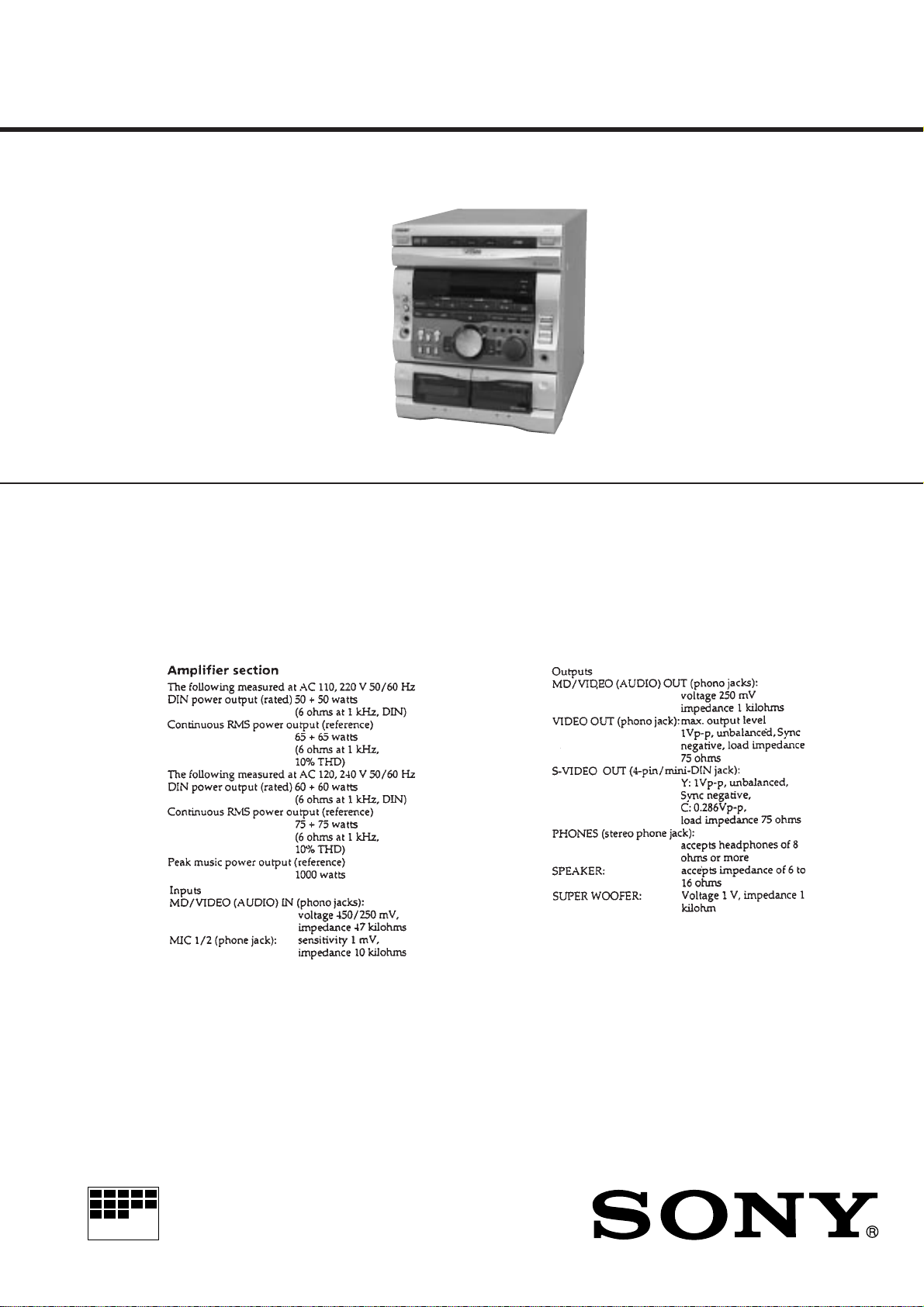
HCD-V515
SERVICE MANUAL
HCD-V515 is the Amplifier, Video CD
player, Tape Deck and Tuner section in
MHC-V515.
Dolby noise reduction manufactured under license
from Dolby Laboratories Licensing Corporation.
“DOLBY” and the double-D symbol a are trademarks of Dolby Laboratories Licensing Corporation.
E Model
Chinese Model
• HCD-V515 is almost same as HCD-V717.
This manual contains only the points which differ
from HCD-V717.
Please refer to HCD-V717 service manual (9-922-879-∏ )
previously issued for other information.
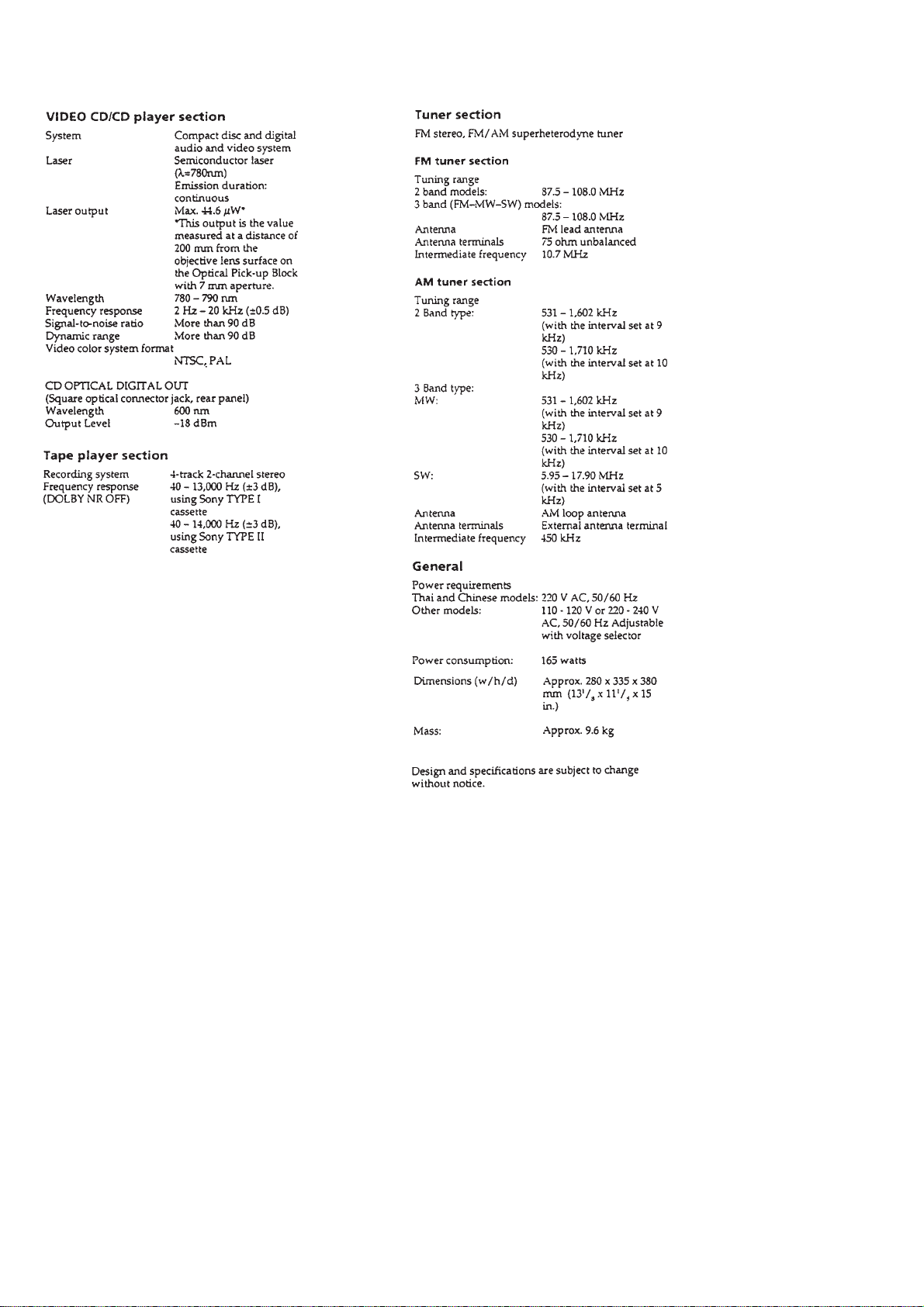
SPECIFICATIONS
– Continued on next page –
MICROFILM
MINI Hi-Fi COMPONENT SYSTEM
– 2 –
SECTION 1
SERVICING NOTES
TABLE OF CONTENTS
1. SERVICING NOTES............................................... 3
2. GENERAL
Location of Controls ....................................................... 5
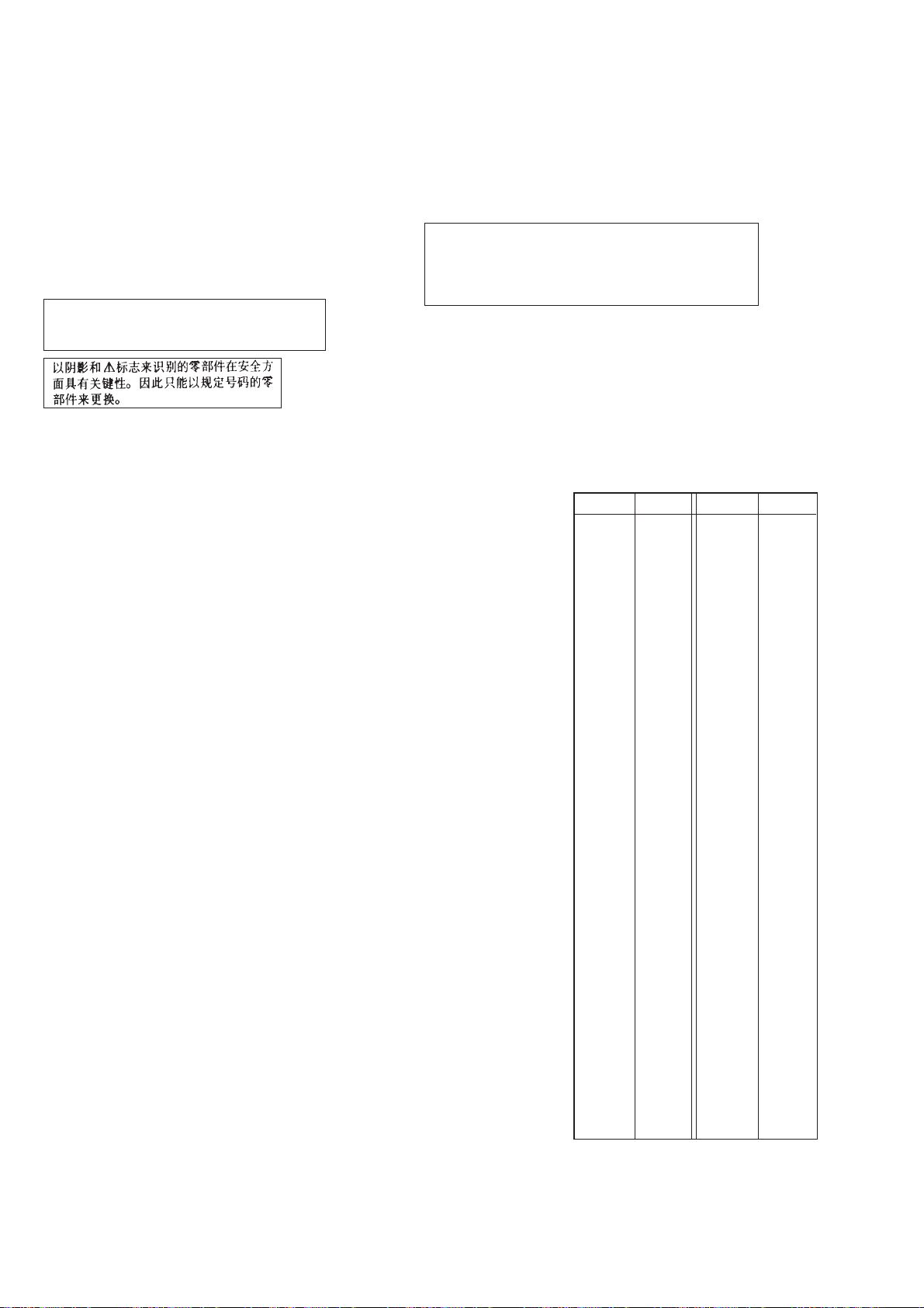
Setting the Time .............................................................. 6
3. DIAGRAMS
3-1. Note for Printed Wiring Boards and
Schematic Diagrams ....................................................... 8
3-2. Printed Wiring Board – MAIN Section –...................... 9
3-3. Schematic Diagram – MAIN Section (1/4) –............... 11
3-4. Schematic Diagram – MAIN Section (2/4) –................ 13
3-5. Schematic Diagram – MAIN Section (3/4) –................ 15
3-6. Schematic Diagram – MAIN Section (4/4) –................ 17
3-7. Printed Wiring Board – PANEL Section –.................... 19
3-8. Schematic Diagram – PANEL Section – ....................... 21
3-9. Printed Wiring Board – POWER AMP Section – ......... 24
3-10. Schematic Diagram – POWER AMP Section –............ 25
3-11. Printed Wiring Board
– TRANSFORMER Section – ........................................ 27
3-12. Schematic Diagram
– TRANSFORMER Section – ........................................ 28
4. EXPLODED VIEWS................................................ 29
5. ELECTRICAL PARTS LIST ............................... 33
NOTES ON HANDLING THE OPTICAL PICK-UP
BLOCK OR BASE UNIT
The laser diode in the optical pick-up block may suffer electrostatic break-down because of the potential difference generated
by the charged electrostatic load, etc. on clothing and the human
body.
During repair, pay attention to electrostatic break-down and also
use the procedure in the printed matter which is included in the
repair parts.
The flexible board is easily damaged and should be handled with
care.
NOTES ON LASER DIODE EMISSION CHECK
The laser beam on this model is concentrated so as to be focused
on the disc reflective surface by the objective lens in the optical
pick-up block. Therefore, when checking the laser diode emission, observe from more than 30 cm away from the objective lens.
Notes on chip component replacement
• Never reuse a disconnected chip component.
• Notice that the minus side of a tantalum capacitor may be damaged by heat.
Flexible Circuit Board Repairing
• Keep the temperature of the soldering iron around 270 ˚C during repairing.
• Do not touch the soldering iron on the same conductor of the
circuit board (within 3 times).
• Be careful not to apply force on the conductor when soldering
or unsoldering.
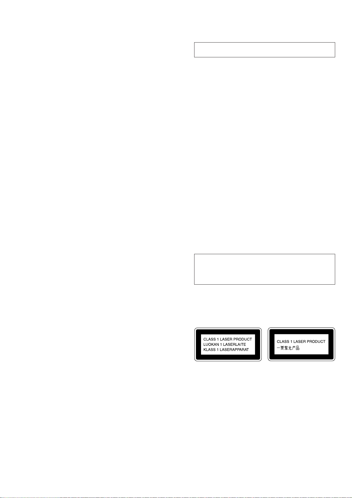
CAUTION
Use of controls or adjustments or performance of procedures
other than those specified herein may result in hazardous radiation exposure.
This appliance is classified as a CLASS 1 LASER product.
The CLASS 1 LASER PRODUCT MARKING is located on
the rear exterior.
Laser component in this product is capable of emitting radiation
exceeding the limit for Class 1.
The following caution label is located inside the unit.
– 3 –
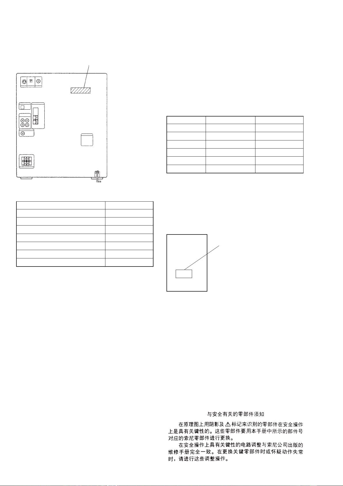
MODEL IDENTIFICATION
– Back Panel –
PART No.
MODEL PART No.
Malaysia and Singapore models 4-999-906-0π
Saudi Arabia model 4-999-906-1π
Chinese model 4-999-906-2π
Hong Kong model 4-999-906-3π
Taiwan model 4-999-906-4π
Indonesia model 4-999-906-5π
Thai model 4-999-906-9π
IC502 OF VIDEO BOARD
IC502 of the VIDEO board consists of the former type and new
type. The following table shows the differences between the two
types.
Only spare parts for the new type IC502 are supplied.
Units using the former IC502 will not function when replaced with
the new type without performing the following procedure.
Consequently, replace IC502 of units using the former type according to the following procedure.
Table of Differences
FORMER TYPE NEW TYPE
C407, 408 MOUNT NO MOUNT
IC502 M30620MC-302FP M30620MC-305FP
JW421, JW422 NO MOUNT MOUNT
IC402 MOUNT NO MOUNT
R413, 421, 422 MOUNT NO MOUNT
X401 MOUNT NO MOUNT
Replacing Procedure
1. Remove IC402.
2. Solder JW421 and JW422, or short-circuit with a lead wire,
etc.
3. Replace IC502 with a new one.
How to Differentiate
[VIDEO board] (Side A)
Those with IC402 : FORMER TYPE
Those without IC402: NEW TYPE
SAFETY-RELATED COMPONENT WARNING!!
COMPONENTS IDENTIFIED BY MARK ! OR DOTTED
LINE WITH MARK ! ON THE SCHEMATIC DIA GRAMS
AND IN THE PARTS LIST ARE CRITICAL TO SAFE
OPERATION. REPLACE THESE COMPONENTS WITH
SONY PARTS WHOSE PART NUMBERS APPEAR AS
SHOWN IN THIS MANU AL OR IN SUPPLEMENTS PUBLISHED BY SONY.
– 4 –
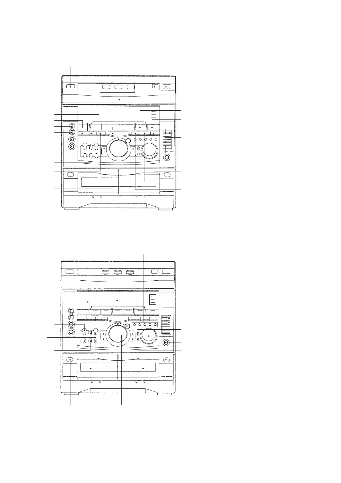
LOCATION OF CONTROLS
• Front view
SECTION 2
GENERAL
!∞
!§
!¶
!•
!ª
@º
@¡
@™
@£
@¢
@∞
1 2
3 4
5
6
7
8
9
!º
!¡
!™
!£
!¢
1 I /u (Power) button
2 DISC 1 to 3 buttons and indicators
3 DISC SKIP/EX-CHANGE button
4 6 (CD) button
5 CD disc tray
6 CD ^ button and indicator
7 TUNER, BAND button
8 r REC button and indicator
9 P PAUSE button and indicator
!º HI-DUB button
!¡ CD SYNC button
!™ FILE SELECT button
!£ SURROUND button
!¢ KARAOKE PON/MPX button
!∞ DECK B 9 and ( buttons and indicators
!§ DECK A 9 and ( buttons and indicators
!¶ FUNCTION button
!• ECHO LEVEL knob
!ª MIC LEVEL knob
@º MIC1 jack
@¡ MIC2 jack
@™ DISPLAY/DEMO button
@£ CLOCK/TIMER SET button
@¢ TIMER SELECT button
@∞ p button
#¶
#¢
#∞
#§
#•
#ª
$º
@§ @¶ @•
$¡ $™ $£ $¢ $∞ $§ $¶
@ª
#º
#¡
#™
#£
@§ Fluorescent indicator tube
@¶ ENTER/NEXT button and indicator
@• A CTIVE, SELECT , RETURN, PREV, NEXT b utton
@ª VIDEO CD, PBC, PBC OFF indicators
#º GROOVE button and indicator
#¡ VOLUME konb
#™ PHONES jack
#£ DBFB button
#¢ Remote sensor
#∞ CD LOOP button
#§ CD NON-STOP button and indicator
#¶ CD FLASH button
#• EDIT, DIRECTION button
#ª PLAY MODE, DOLBY NR button
$º REPEAT button
$¡ § button (deck A)
$™ Tape deck A
$£ –, 0 button and indicator
$¢ JOG dial
$∞ +, ) button and indicator
$§ Tape deck B
$¶ § button (deck B)
– 5 –
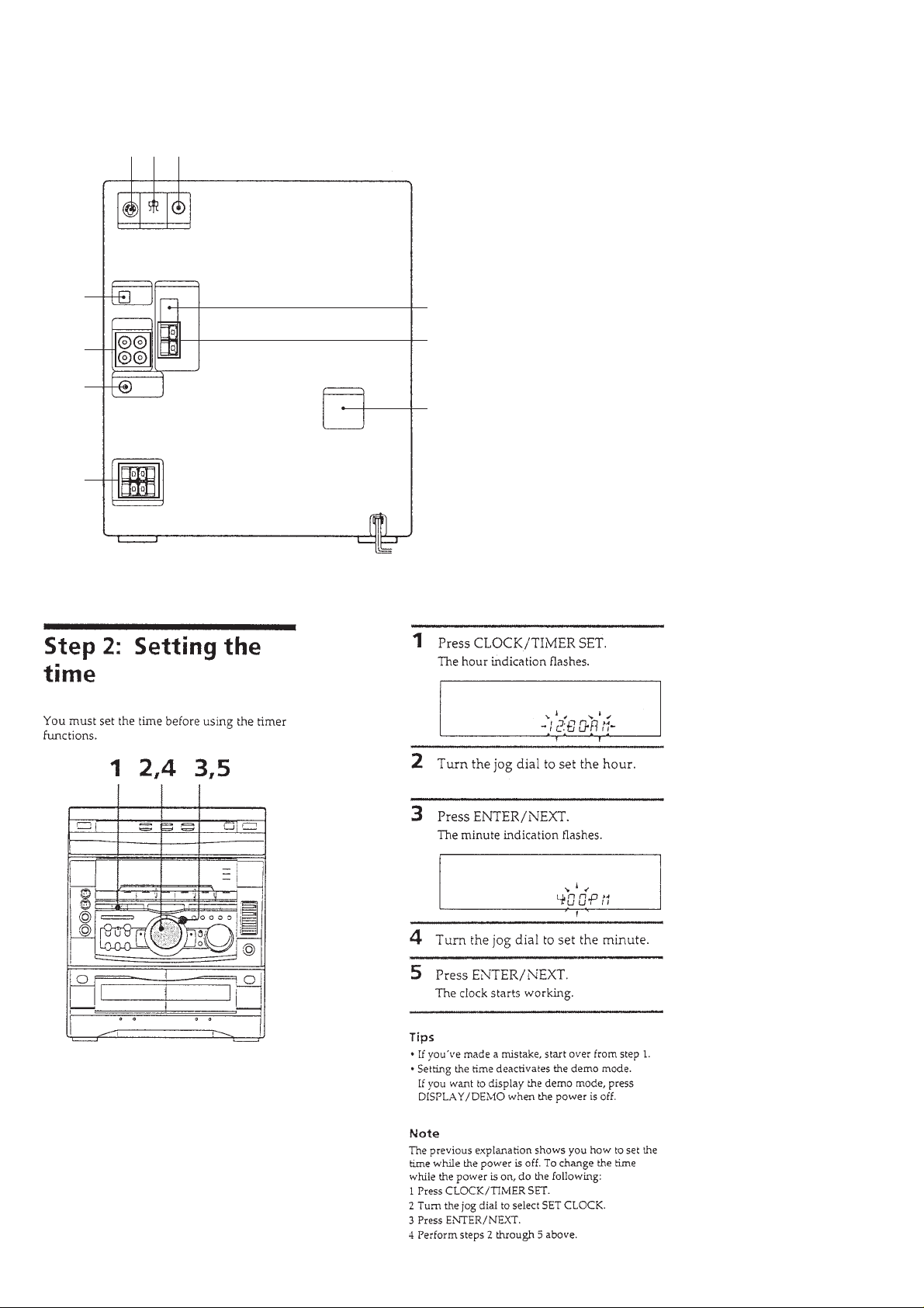
• Rear view
7
8
9
!º
1
2 3
4
5
6
1 S VIDEO OUT jack
2 SYSTEM SELECT switch
3 VIDEO OUT jack
4 FM antenna terminal
5 AM antenna terminal
6 VOLTAGE SELECTOR switch
(EXCEPT Thai and Chinese models)
7 CD DIGITAL OUT, OPTICAL connector
8 MD/VIDEO (AUDIO), IN/OUT jacks
9 SUPER WOOFER jack
!º SPEAKER terminals
– 6 –
SECTION 3
DIAGRAMS
3-1. NOTE FOR PRINTED WIRING BOARDS AND SCHEMATIC DIAGRAMS
Note on Schematic Diagrams:
• All capacitors are in µF unless otherwise noted. pF: µµF
50 WV or less are not indicated except for electrolytics
and tantalums.
• All resistors are in Ω and 1/
specified.
¢
•
• 2 : nonflammable resistor.
• 5 : fusible resistor.
• C : panel designation.
• U : B+ Line.
• V : B– Line.
• V oltages are taken with a V OM (Input impedance 10 MΩ).
• Waveforms are taken with a oscilloscope.
• Circled numbers refer to waveforms.
• Signal path.
• Abbreviation
: internal component.
The components identified by mark ! or dotted
line with mark ! are critical for safety.
Replace only with part number specified.
Voltage variations may be noted due to normal production tolerances.
Voltage variations may be noted due to normal production tolerances.
F : TUNER (FM/AM)
E : PLAYBACK (DECK A)
d : PLAYBACK (DECK B)
G : RECORD
J : CD PLAY (AUDIO)
L : CD PLAY (VIDEO)
c : DIGITAL OUT
N : MIC INPUT
CH : Chinese model.
TH : Thai model.
4
W or less unless otherwise
Note on Printed Wiring Boards:
• X : parts extracted from the component side.
®
•
• b : Pattern from the side which enables seeing.
(The other layers' patterns are not indicated.)
Caution:
Pattern face side: Parts on the pattern face side seen from
(Side B) the pattern face are indicated.
Parts face side: Parts on the par ts face side seen from
(Side A) the parts face are indicated.
: Through hole.
• Semiconductor Location
Ref. No. Location
D141 G-9
D333 E-2
D334 F-2
D401 G-10
D501 E-5
D502 E-5
D503 E-5
D504 E-5
D505 E-6
D506 E-6
D507 F-3
D508 F-2
D901 I-6
D902 I-5
D903 I-6
D904 I-6
D905 G-6
D906 G-7
D907 H-4
D908 H-4
D909 I-5
D910 I-4
D911 I-4
D912 I-4
D913 G-3
D914 G-5
D915 I-3
D-917 F-7
D-918 G-4
IC101 D-9
IC102 F-10
IC191 D-11
IC301 B-2
IC381 A-11
IC501 D-4
IC502 E-6
IC901 G-5
IC902 G-3
IC903 H-3
IC904 F-4
Q111 F-9
Q112 F-9
Ref. No. Location
Q113 H-8
Q161 E-8
Q162 D-8
Q163 H-8
Q191 D-11
Q331 C-2
Q332 D-2
Q333 C-2
Q334 D-2
Q335 C-1
Q336 E-2
Q337 E-2
Q338 F-2
Q339 F-2
Q340 E-2
Q341 E-2
Q342 E-2
Q343 E-2
Q431 G-9
Q432 H-8
Q433 H-9
Q434 H-8
Q435 H-8
Q436 G-8
Q437 G-8
Q501 E-7
Q571 E-6
Q572 E-6
Q575 F-8
Q901 F-6
Q902 G-6
Q903 H-6
Q905 F-6
Q906 G-6
Q907 G-4
Q908 G-5
Q909 H-4
Q910 I-4
Q911 F-3
Q912 F-3
Q913 G-6
Q914 F-7
Q951 G-7
Q952 G-7
– 8 –
3-2. PRINTED WIRING BOARD – MAIN Section –
HCD-V515
(See page
46 on HCD V717 service
manual)
(See page
50 on HCD V717 service
manual)
(See page 41 on
HCD-V717
service manual)
(See page 41 on
HCD-V717
service manual)
JW395
JW394
(TH, CH)
(
EXCEPT
(
TH,CH
JW509
(See page 36 on
HCD-V717
service manual)
1
JW042
JW396
VIDEO BOARD
CN503
JW503
1
7
IC382
8
14
13
12
JW239
R395
(Page 19)
(See page 67 on
HCD-V717
service manual)
D334
D508
D333
Q911
E
C
B
R917
C923
C915
C916
R916
Q912
B
C
E
IC904
C922
D918
R918
R919
D917
(EXCEPT CH)
(EXCEPT CH)
(CH)
SPEAKER
IMPEDANCE
USE 6-16Ω
– 9 –
POWER ANP BOARD
CN801
(Page 24)(Page 27)
11
13
HCD-V515 MAIN
– 10 –
HCD-V515
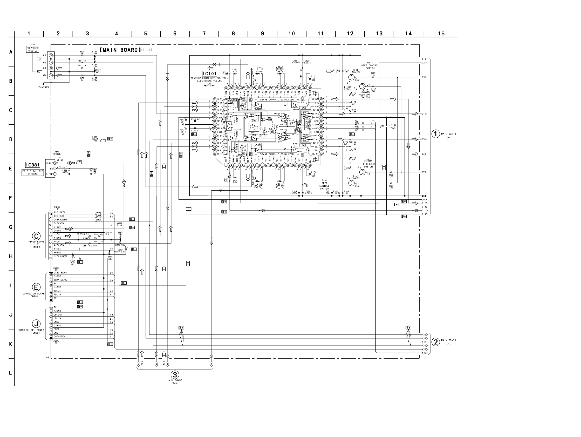
3-3. SCHEMATIC DIAGRAM – MAIN Section (1/4) –
(Page 13)
(See Page 37
on HCD-V717
Service manual)
(See Page 44
on HCD-V717
Service manual)
(See Page 44
on HCD-V717
Service manual)
(Page 17)
(Page 15)
• Voltages and waveforms are dc with respect to ground
under no-signal (detuned) conditions.
no mark : FM
( ) : CD
– 11 –
– 12 –
 Loading...