

Page 1
HCD-GRX9900/RXD9
SERVICE MANUAL
HCD-GRX9900/RDX9 are the Amplifier,
CD player, Tape Deck and Tuner section
in MHC-GRX9900/RXD9.
Dolby noise reduction manufactured under license
from Dolby Laboratories Licensing Corporation.
“DOLBY” and the double-D symbol a are trademarks of Dolby Laboratories Licensing Corporation.
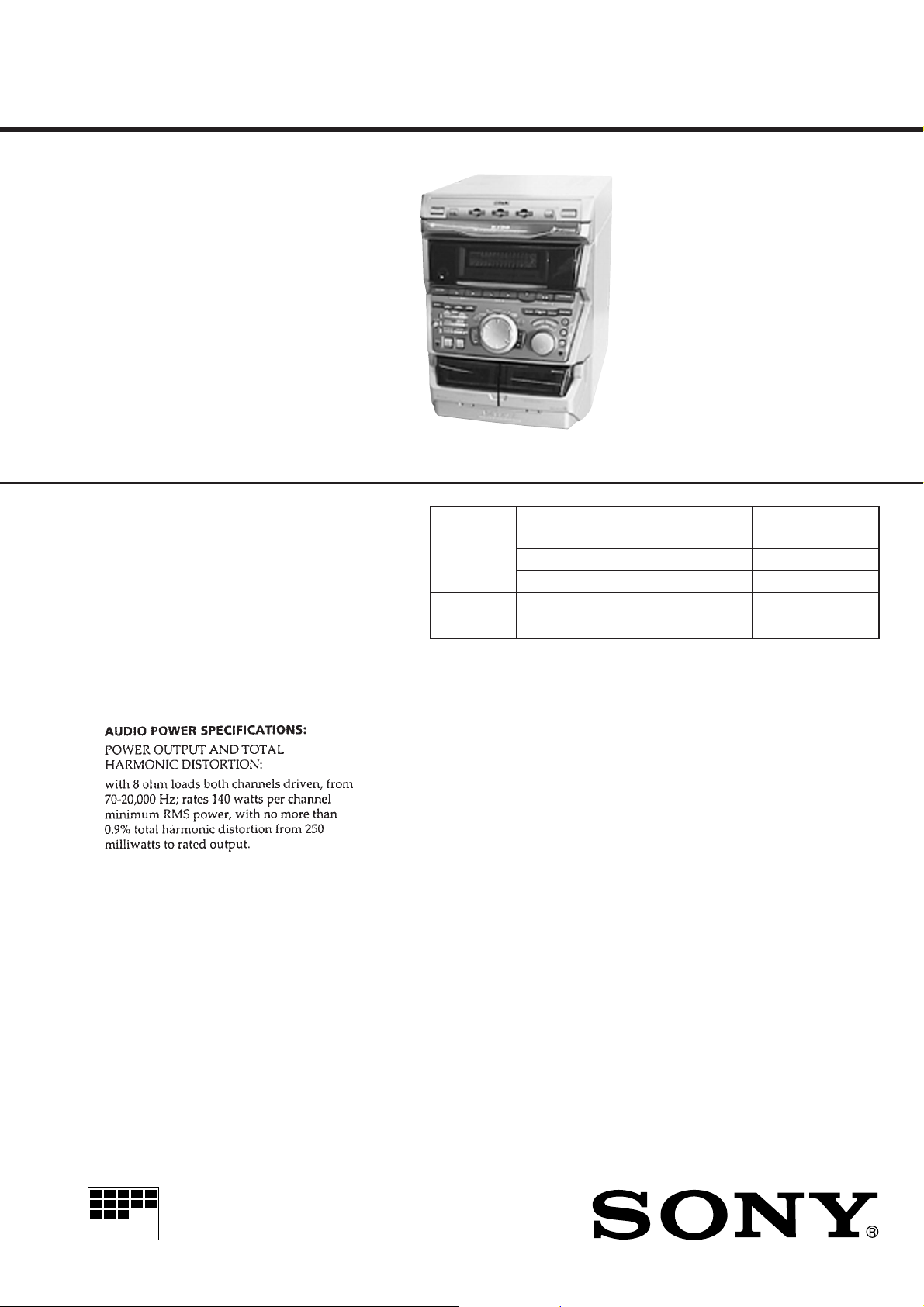
Photo: HCD-RXD9 (US model)
CD
Section
Tape deck
Section
US Model
AEP Model
UK Model
HCD-RXD9
E Model
HCD-GRX9900
Model Name Using Similar Mechanism NEW
CD Mechanism Type CDM38LH-5BD32L
Base Unit Name BU-5BD32L
Optical Pick-up Name KSS-213D/Q-NP
Model Name Using Similar Mechanism NEW
Tape Transport Mechanism Type TCM-230AWR2
Amplifier section
US model:
AEP and UK models:
DIN power output (rated) 120 + 120 watts
(8 ohms at 1 kHz, DIN)
Continuous RMS power output (reference)
150 + 150 watts
(8 ohms at 1 kHz, 10% THD)
Music power output (reference)
275 + 275 watts
(8 ohms at 1 kHz, 10% THD)
SPECIFICATIONS
E models:
The following measured at AC 120, 220, 240 V 50/60 Hz
DIN power output (rated) 200 + 200 watts
(6 ohms at 1 kHz, DIN)
Continuous RMS power output (reference)
250 + 250 watts
(6 ohms at 1 kHz, 10% THD)
– Continued on next page –
MICROFILM
MINI Hi-Fi COMPONENT SYSTEM
Page 2
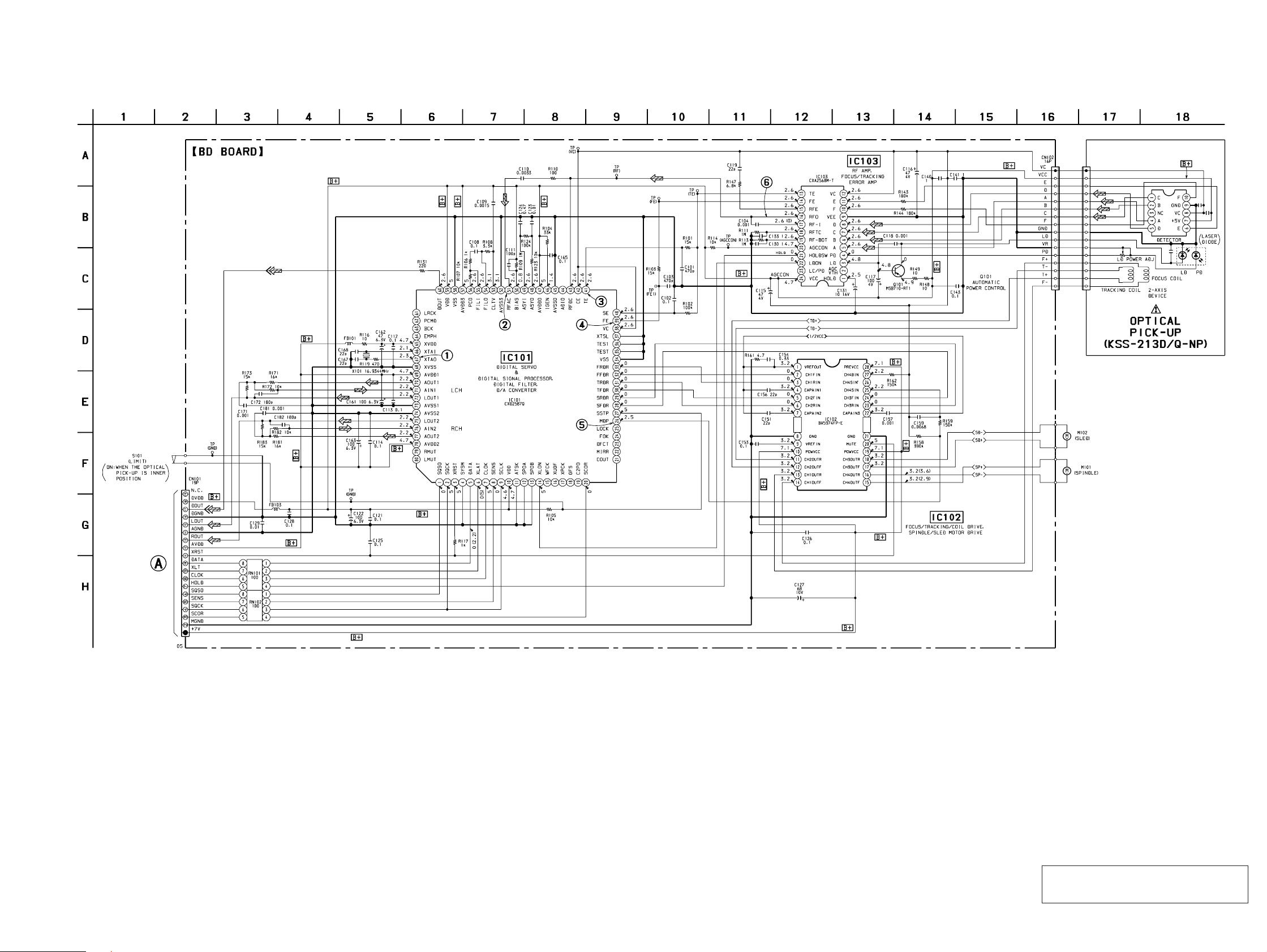
7-7. SCHEMATIC DIAGRAM – BD Board – • See page 65 for Waveforms. • See page 66 for IC Block Diagrams.
HCD-GRX9900/RXD9
(Page 45)
• Voltages and waveforms are dc with respect to ground
under no-signal conditions.
no mark : CD STOP
( ) : CD PLAY
The components identified by mark ! or dotted
line with mark ! are critical for safety.
Replace only with part number specified.
– 31 –
– 32 –
Page 3
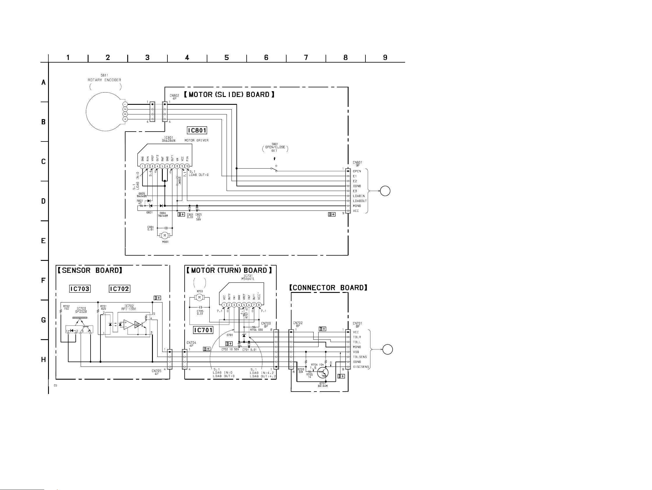
7-9. SCHEMATIC DIAGRAM – CD MOTOR Section – • See page 67 for IC Block Diagrams.
DISC TRAY
ADDRESS DETECT
DISC TRAY SLIDE
CLOSE
OPEN
HCD-GRX9900/RXD9
DISC IN DETECT
SENSOR
DISC TRAY
SENSOR
MTZJ-T-72
(DISC TRAY SLIDE)
DISC
TRAY
TURN
DISC TRAY TURN
MOTOR DRIVER
B
(Page 45)
MTZJ-T-72
C
(Page 45)
– 35 –
LEVEL SHIFT
• Voltages are dc with respect to ground under no-signal
conditions.
no mark : CD STOP
– 36 –
Page 4
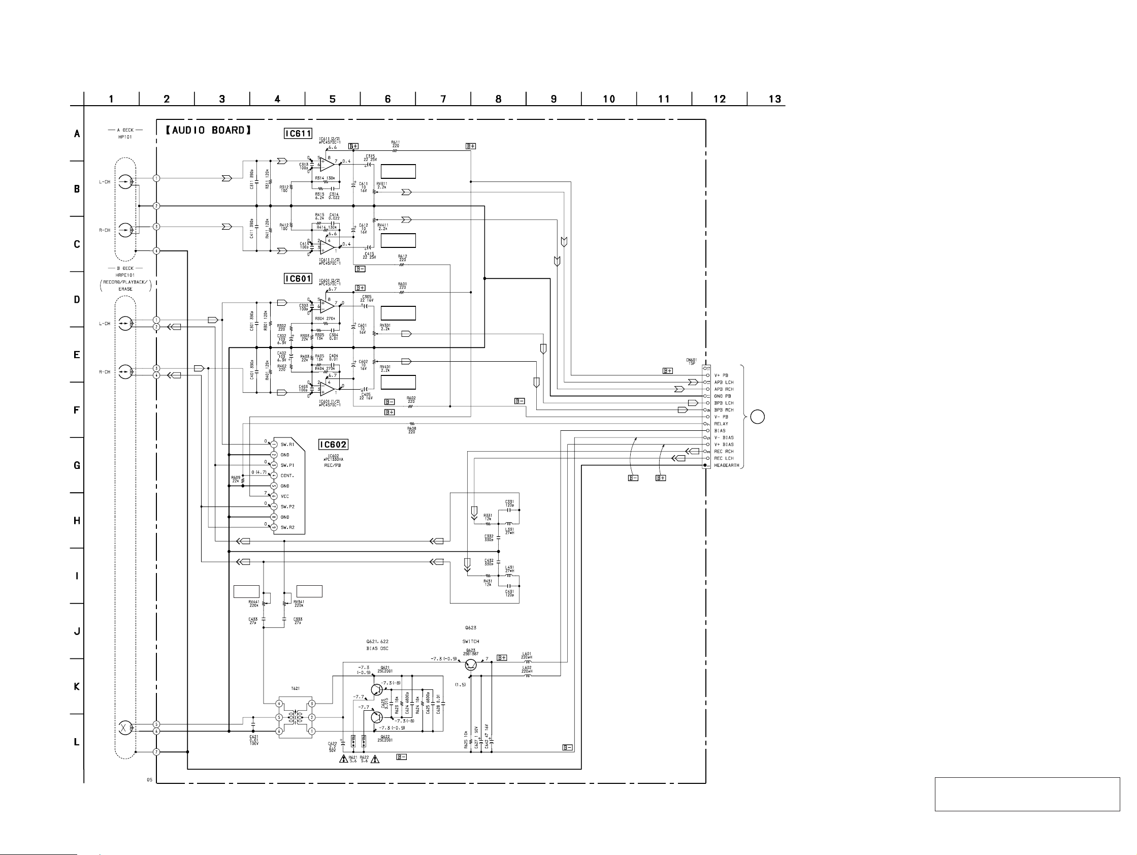
7-11. SCHEMATIC DIAGRAM – AUDIO Board – • See page 68 for IC Block Diagram.
HCD-GRX9900/RXD9
(PLAYBACK)
PB EQ AMP
(DECK A)
PB EQ AMP
(DECK B)
PB LEVEL (L)
(DECK A)
PB LEVEL (R)
(DECK A)
PB LEVEL (L)
(DECK B)
PB LEVEL (R)
(DECK B)
D
(Page 49)
REC BIAS (R)
(DECK B)
BIAS OSC
REC BIAS (L)
(DECK B)
SWITCHING
REC BIAS
-6.8
– 39 –
• Voltages are dc with respect to ground under no-signal
conditions.
no mark : TAPE PLAY
( ) : RECORD
– 40 –
The components identified by mark ! or dotted
line with mark ! are critical for safety.
Replace only with part number specified.
Page 5
HCD-GRX9900/RXD9
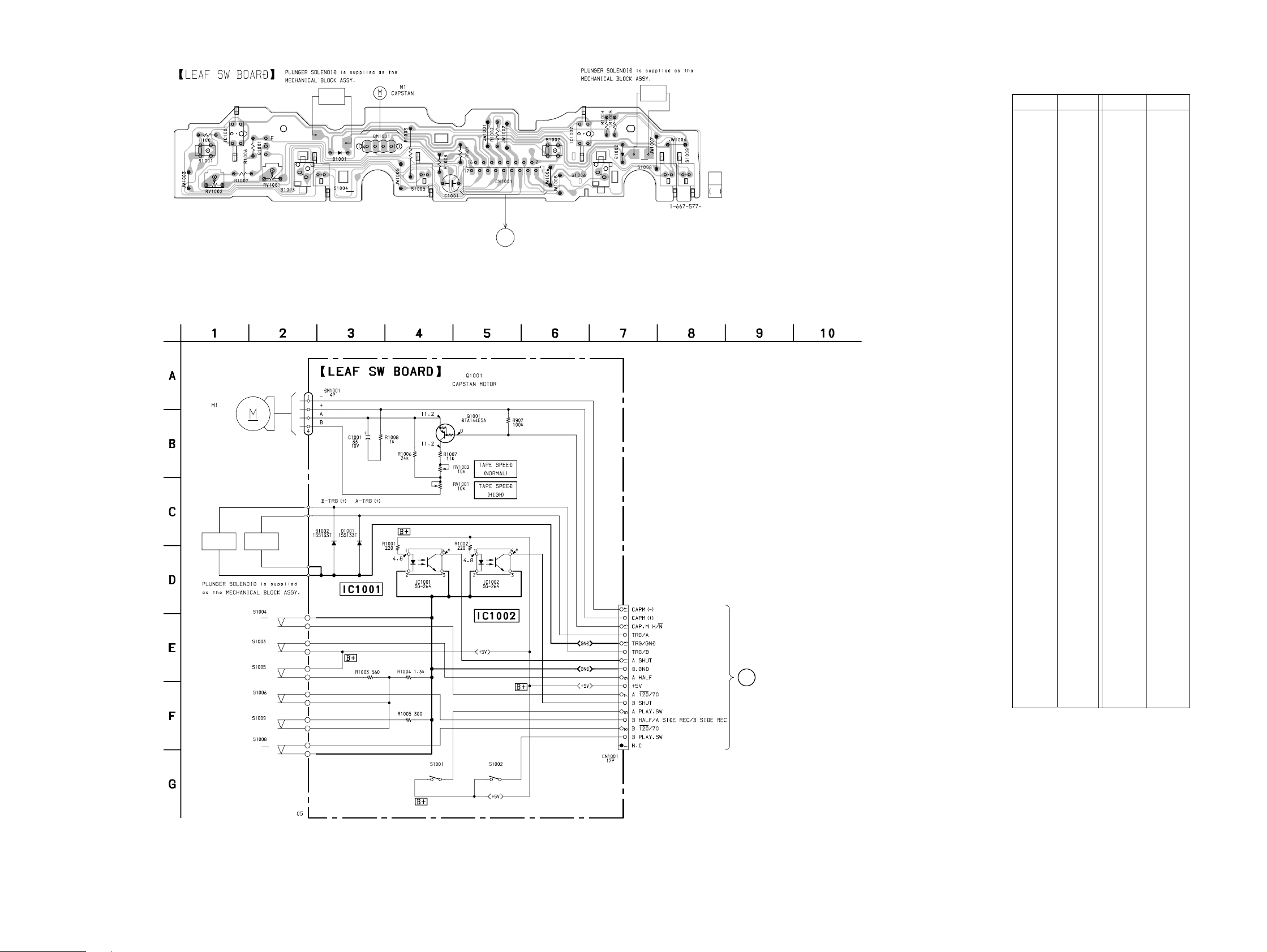
7-12. PRINTED WIRING BOARD – LEAF SW Board – • See page 28 for Circuit Boards Location.
DECK A
PLUNGER
4
3
1
2
(DECK A PLAY)
05
(DECK A HALF)
(DECK A 120/70)
(
)
(DECK A REC)
7-13. SCHEMATIC DIAGRAM – LEAF SW Board –
(CAPSTAN)
DECK B
PLUNGER
DECK A
PLUNGER
(DECK A 120/70)
(DECK A HALF)
(DECK A REC)
(DECK B HALF)
ROTATION DETECT SENSOR
(DECK A)
CONTROL SWITCH
ROTATION DETECT
SENSOR (DECK B)
E
(Page 43)
(DECK B PLAY)
4
1
(DECK B HALF)
DECK B
PLUNGER
3
2
(DECK B 120/70)
(DECK B REC)
21
21
• Semiconductor Location
Ref. No. LocationRef. No. Location
D141 E-10
D191 E-12
D331 E-1
D333 F-1
D334 E-1
D335 F-1
D401 G-11
D403 F-12
D405 H-6
D406 J-4
D407 I-2
D411 G-3
D501 D-7
D502 E-6
D503 D-6
D504 D-7
D505 D-7
D506 D-7
D509 F-2
D607 E-5
D644 C-8
D801 J-11
D802 G-9
D803 G-11
D831 I-6
D832 J-7
D851 J-10
D852 G-9
D881 H-9
D901 J-4
D902 J-4
D903 J-4
D904 I-4
D905 I-1
D906 H-1
D907 J-5
D908 I-5
D909 J-5
D910 J-5
D915 I-4
D921 H-4
D922 G-4
D923 G-4
D924 F-2
D925 G-4
Q113 E-9
Q161 C-9
Q162 C-9
Q163 E-9
Q191 E-12
Q192 E-10
Q201 D-9
Q251 C-9
Q331 C-1
Q332 C-2
Q333 C-2
Q334 C-2
Q335 D-1
Q336 F-1
Q337 F-1
Q338 F-1
Q339 F-1
Q340 E-1
Q341 E-1
Q342 F-1
Q343 E-1
Q401 F-12
Q402 E-12
Q411 G-2
Q412 G-3
Q431 G-12
Q432 G-11
Q433 F-11
Q434 F-11
Q435 F-11
Q436 F-11
Q437 G-12
Q439 F-12
Q471 F-2
Q501 D-7
Q508 D-7
Q509 E-7
Q801 H-10
Q803 G-10
Q804 G-9
Q831 G-10
Q832 G-10
Q851 J-10
Q881 I-9
Q901 H-2
Q902 I-1
Q903 H-1
Q904 G-4
Q905 G-4
Q907 G-5
Q908 G-4
Q909 I-4
Q913 H-1
Q914 G-2
Q923 H-1
Q951 G-2
Q952 H-1
E
(Page 49)
IC101 C-10
IC301 B-3
IC381 A-12
IC501 D-5
IC502 D-7
IC801 H-10
IC901 G-6
IC902 G-4
IC903 H-4
Q111 D-10
Q112 D-10
(DECK B REC)
(DECK B 120/70)
• Voltages are dc with respect to ground under no-signal
conditions.
no mark : TAPE PLAY
( ) : RECORD
: Impossible to measure
∗
– 41 –
(DECK A PLAY)
(DECK B PLAY)
– 42 –
Page 6
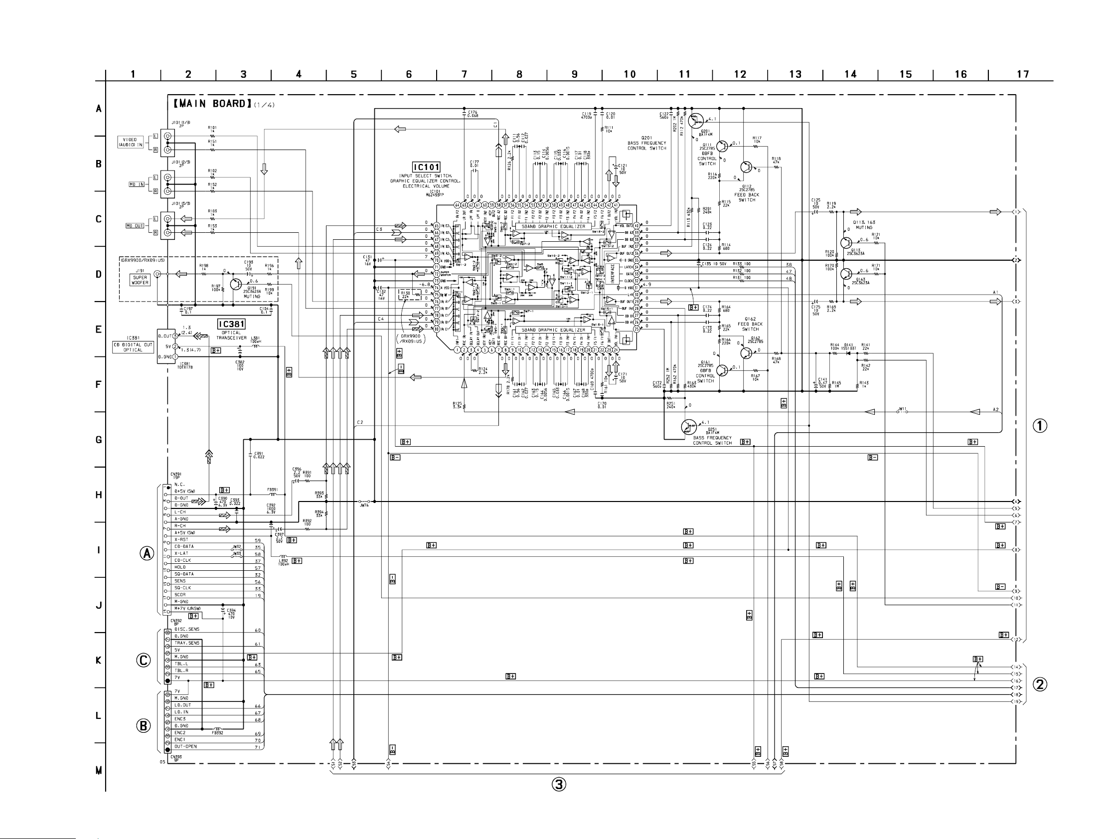
HCD-GRX9900/RXD9
7-15. SCHEMATIC DIAGRAM – MAIN Board (1/4) –
• Voltages and waveforms are dc with respect to ground
under no-signal (detuned) conditions.
no mark : TUNER (FM/AM)
( ) : CD PLAY
(Page 31)
(Page 36)
(Page
47)
(Page
51)
(Page 36)
– 45 –
(Page 50)
– 46 –
Page 7

7-16. SCHEMATIC DIAGRAM – MAIN Board (2/4) –
HCD-GRX9900/RXD9
(Page
46)
(Page
50)
(Page 61)
(Page 52)
– 47 –
• Voltages are dc with respect to ground under no-signal
(detuned) conditions.
no mark : FM
– 48 –
The components identified by mark ! or dotted
line with mark ! are critical for safety.
Replace only with part number specified.
Page 8

HCD-GRX9900/RXD9
7-17. SCHEMATIC DIAGRAM – MAIN Board (3/4) –
(Page 46)
(Page 47)
(Page 51)
(Page 62)
(Page 64)
(Page 40)
(Page 58)
(Page 51)
• Voltages are dc with respect to ground under nosignal (detuned) conditions.
no mark : TUNER (FM/AM)
( ) : CD PLAY
{ } : TAPE PLAYBACK (DECK A)
[ ] : TAPE PLAYBACK (DECK B)
〈〈 〉〉 : RECORD
– 49 –
(Page 42)
– 50 –
Page 9

7-18. SCHEMATIC DIAGRAM – MAIN Board (4/4) – • See page 65 for Waveforms.
(Page
46)
(Page
50)
• Voltages and waveforms are dc with respect to ground
under no-signal (detuned) conditions.
no mark : TUNER (FM/AM)
( ) : CD PLAY
{ } : TAPE PLAYBACK (DECK A)
[ ] : TAPE PLAYBACK (DECK B)
〈〈 〉〉 : RECOARD
(Page 48)
HCD-GRX9900/RXD9
(Page
50)
– 51 –
– 52 –
Page 10

7-20. SCHEMATIC DIAGRAM – PANEL (1/3)/CD SW Board– • See page 68 for IC Block Diagrams.
HCD-GRX9900/RXD9
– 55 –
• Voltages and waveforms are dc with respect to ground
(Page 57)(Page 59)(Page 59)
under no-signal (detuned) conditions.
no mark : TUNER (FM/AM)
– 56 –
Page 11

HCD-GRX9900/RXD9
7-21. SCHEMATIC DIAGRAM – PANEL (2/3) Board– • See page 65 for waveform.
(Page 56)
• Voltages and waveforms are dc with respect to ground
under no-signal (detuned) conditions.
no mark : TUNER (FM/AM)
(Page 59)
(Page 50)
(Page 60)
– 57 –
– 58 –
Page 12

7-22. SCHEMATIC DIAGRAM – PANEL (3/3) Board– • See page 68 for IC Block Diagrams.
HCD-GRX9900/RXD9
(Page 57)
(Page 58)
(Page 55)
(Page 55)
– 59 –
• Voltages and waveforms are dc with respect to ground
under no-signal (detuned) conditions.
no mark : TUNER (FM/AM)
– 60 –
Page 13

HCD-GRX9900/RXD9
7-23. PRINTED WIRING BOARD – TRANS Board –
• See page 28 for Circuit Boards Location.
7-24. SCHEMATIC DIAGRAM – TRANS Board –
(Page 63)
(Page 48)
(Page 50)
(Page 64)
• Voltages are dc with respect to ground under no-signal
(detuned) conditions.
no mark : TUNER (FM/AM)
The components identified by mark ! or dotted
line with mark ! are critical for safety.
Replace only with part number specified.
(Page 43)
(Page 43)
– 61 –
• Semiconductor
Location
Ref. No. Location
D971 G-2
D972 G-1
D973 G-1
Q971 G-1
– 62 –
Page 14

HCD-GRX9900/RXD9
7-25. PRINTED WIRING BOARD – SUB TRANS Board (RXD9) –
• See page 28 for Circuit Boards Location.
7-26. SCHEMATIC DIAGRAM – SUB TRANS Board (RXD9) –
(Page 62)
(Page
50)
K
(Page 61)
• Semiconductor
Location
Ref. No. Location
D11 C-2
D12 C-2
D13 C-1
D14 C-2
D15 C-2
D16 E-3
D17 D-2
D18 D-2
D19 D-2
D20 D-2
D21 D-2
D22 D-1
D23 D-1
• Voltages are dc with respect to ground under no-signal
(detuned) conditions.
no mark : TUNER (FM/AM)
The components identified by mark ! or dotted
line with mark ! are critical for safety.
Replace only with part number specified.
(Page 43)
– 63 –
IC11 D-3
Q11 E-2
Q12 D-2
Q13 D-2
Q14 D-1
Q15 D-1
Q16 D-1
Q17 D-1
– 64 –
Page 15

• Waveforms
– BD Board –
1 IC101 ^¶ (XTAO)
5 IC101 @§ (MDP)
– MAIN Board –
1 IC501 0 (XC-IN)
• IC Block Diagrams
– BD Board –
IC101 CXD2587Q
3.1 Vp-p
16.9344 MHz
2 IC101 %¡ (RF AC) (CD Play Mode)
3 IC101 $¡ (TE) (CD Play Mode)
1.2 Vp-p
2.5 Vp-p
7.8 µs
32.768 kHz
6 IC102 !§ (RFO) (CD Play Mode) 2 IC501 !∞ (XIN)
1.3 Vp-p
16 MHz
– PANEL Board –
1 IC601 &™ (XOUT)
1.8 Vp-p
2.2 Vp-p
LRCK
PCMD
BCK
EMPH
XVDD
XTAI
XTAO
XVSS
AVDD1
AOUT1
AIN1
LOUT1
AVSS1
AVSS2
LOUT2
AIN2
AOUT2
AVDD2
RMUT
LMUT
VDD
AVDD3
DOUT
60
DIGITAL
OUT
61
62
63
64
65
66
67
68
69
70
71
72
73
74
75
76
77
78
79
80
D/A
INTERFACE
TIMING
LOGIC
OVER SAMPLING
PWM
3rd ORDER
NOISE SHAPER
DIGITAL FILTER
SERIAL IN
INTERFACE
59
58
INTERNAL BUS
PWM
VSS
57
ERROR
CORRECTOR
16K
RAM
SUBCODE
PROCESSOR
FILO
FILI
PCO
54
56
55
53
DIGITAL
PLL
EFM
DEMODULATOR
SERVO
INTERFACE
SERVO AUTO
SEQUENCER
CLTV
AVSS3
52
ASYI
BIAS
RFAC
51
49
50
ASYMMETRY
CORRECTION
48
ASYO
47
AVDD0
46
IGEN
AVSS0
45
ADIO
44
SERVO DSP
FOCUS
SERVO
TRACKING
SERVO
SLED
SERVO
CE
TE
RFDC
43
41
42
OPERATIONAL
AMPLIFIER
ANALOG SWITCH
A/D
CONVERTER
PWM GENERATOR
CLOCK
GENERATOR
FOCUS PWM
GENERATOR
TRACKING
PWM GENERATOR
SLED PWM
GENERATOR
DIGITAL
CLV
MIRR, DFCT,
FOK
DETECTOR
SE
40
FE
39
VC
38
XTSL
37
TES1
36
TEST
35
VSS
34
33
FRDR
32
FFDR
TRDR
31
TFDR
30
SRDR
29
28
SFDR
SSTP
27
MDP
26
25
LOCK
FOK
24
DFCT
23
22
MIRR
4 IC101 #ª (FE) (CD Play Mode)
0.2 Vp-p
0.5 Vp-p
12.5 MHz
4.7 Vp-p
1
2
SQSO
SQCK
3
XRST
4
SYSM
CPU
INTERFACE
7
5
6
XLAT
DATA
8
CLOK
SENS
9
10
SCLK
11 12
VDD
ATSK
13
SPOA
14
SPOB
1516171819
XUGF
XPCK
XLON
WFCK
GFS
20
C2PO
SCOR
COUT
21
– 65 –
– 66 –
Page 16

IC103 CXA2568M-T6
HOLD
AGC VTH
VEE
+
–
VC
VC
VCC
APC LD AMP
50µA
+
–
+
–
VEE
RF SUMMING AMP
+
–
FOCUS ERROR AMP
+
–
VCC
+
–
VCC
VC
+
–
VC
RF EQ AMP
+
–
+
–
1
VEE
2
LD
3
4
PD
5
A
6
B
7
C
D
8
9
VC
10
F
APC PD AMP
+
–
+
–
VEE
–
+
VC
VEE
VC
+
–
24
23
22
21
20
19
18
17
16
15
14
VCC
LC/PD
LD ON
HOLD SW
AGC CONT
RF BOT
RFTC
RF I
RF O
RFE
FE
VC BUFFER
VC
–
+
+
–
E
11
VC
12
VC
– MOTOR (TURN) Board –
IC701 M54641L
VCC
1
2
OUT2
REG
IN1
GND
INPUT
3
AMP.
CONTROL
INPUT
AMP.
4
POWER AMP.
POWER AMP.
VC
VCC
8
OUT1
7
IN2
6
REFERENCE
5
VEE
VCC
VC
–
+
TRACKING
ERROR AMP
TE
13
– MOTOR (SLIDE) Board –
IC801 BA6286N
TSD
POWER
SAVE
CONTROL
LOGIC
GND
RIN
VREF
OUT2
RNF
GND
OUT1
VCC
VM
FIN
1
2
3
4
5
6
7
8
9
10
– 67 –
Page 17

– AUDIO Board –
IC602 µPC1330HA
2
1
SW R1 GND SW P1
3
– PANEL Board –
IC603 BA3830F
4
CONT
INVERTER
COMPARATER
5
VCC
GND
6
SW P2 GND
7 8 9
SW R2
IC604 NJU3716M-T2
R02
R01
LINE NF
LINE IN
REC NF
REC IN
RESET C
BIAS C
GND
2
3
4
5
6
7
8
9
CURRENT
REFERENCE
CURRENT
–
+
–
+
REFERENCE
1
IC711 M65850FP
BAND
PASS
FILTER
RESET
DET
18
17
16
15
14
13
12
11
10
RESET
F01
F02
F03
F04
F05
F06
REC LEVEL
VCC
VDDP6P5P4P3P2VSSP1CLR
2021 192324 22 18 17 16 15 14 13
CONTROL
CIRCUIT
SHIFT REGISTER
LATCH CIRCUIT
OUTPUT CIRCUIT
P11
8
6
7
P12
P13
VSS
21
P7P8P9
43
P10
STB
CLK
DATA
9
11
10
125
P15
P16
SO
P14
1
LPF1IN
VCC
1/2 VCC
AUTO
RESET
LPF1
CLOCK
REF
OSCILLATOR
CLOCK
MAIN
RESET
CONTROL
D1
DO0
A/D
2 345 6 7
OP1IN
OP1OUT
LPF1OUT
DO1
CC1
OP2IN
D/A
MO
MI
OP2OUT
LPF2IN
20KBIT
CC2
LPF2OUT
891014 13 12 11
LPF2
SRAM
GND
– 68 –
 Loading...