

Page 1
HCD-GRX9000/RX900
SERVICE MANUAL
HCD-GRX9000/RX900 are the Amplifier,
CD player, Tape Deck and Tuner section
in MHC-GRX9000/RX900.
Dolby noise reduction manufactured under license
from Dolby Laboratories Licensing Corporation.
“DOLBY” and the double-D symbol a are trademarks of Dolby Laboratories Licensing Corporation.
Photo: HCD-RX900
CD
Section
TAPE
DECK
Section
East European Model
CIS Model
HCD-RX900
E Model
HCD-GRX9000
Model Name Using Similar Mechanism HCD-H991AV
CD Mechanism Type CDM38LH-5BD29AL
Base Unit Type BU-5BD29AL
Optical Pick-up Type KSS-213D/Q-NP
Model Name Using Similar Mechanism HCD-GRX7/RX77S
T ape Transport Mechanism Type
TCM-230AWR1/
230PWR1
SPECIFICATIONS
– Continued on next page –
MICROFILM
MINI Hi-Fi COMPONENT SYSTEM
Page 2
– 2 –
Page 3
TABLE OF CONTENTS
SECTION 1
SERVICING NOTES
1. SERVICING NOTES ............................................... 3
2. GENERAL
Location of Controls ....................................................... 6
Setting the Time .............................................................. 7
3. DISASSEMBLY ......................................................... 8
4. TEST MODE.............................................................. 11
5. MECHANICAL ADJUSTMENTS....................... 13
6. ELECTRICAL ADJUSTMENTS
DECK Section ................................................................. 13
TUNER Section .............................................................. 16
CD Section ...................................................................... 18
7. DIAGRAMS................................................................. 20
7-1. Block Diagram – TUNER Section
(East European, CIS models only) – .............................. 21
7-2. Block Diagram – CD Section – ...................................... 23
7-3. Block Diagram – TAPE DECK Section – ...................... 25
7-4. Block Diagram – MAIN Section (1/2) – ........................ 27
7-5. Block Diagram – MAIN Section (2/2) – ........................ 29
7-6. Block Diagram – DISPLAY/KEY CONTROL/
POWER SUPPLY Section – ........................................... 31
7-7. Note for Printed Wiring Boards and
Schematic Diagrams ....................................................... 33
7-8. Printed Wiring Board – TUNER Section
(East European, CIS models only) – .............................. 34
7-9. Schematic Diagram – TUNER Section
(East European, CIS models only) – .............................. 35
7-10. Printed Wiring Board – CD Section –........................... 37
7-11. Schematic Diagram – CD Section – ............................... 39
7-12. Printed Wiring Boards – CD MOTOR Section – .......... 41
7-13. Schematic Diagram – CD MOTOR Section – .............. 43
7-14. Printed Wiring Board – TAPE DECK Section – ........... 45
7-15. Schematic Diagram – TAPE DECK Section – .............. 47
7-16. Printed Wiring Board – LEAF SW Section – ...............49
7-17. Schematic Diagram – LEAF SW Section – .................. 49
7-18. Printed Wiring Board – MAIN Section –...................... 51
7-19. Schematic Diagram – MAIN Section (1/4) –............... 53
7-20. Schematic Diagram – MAIN Section (2/4) –................ 55
7-21. Schematic Diagram – MAIN Section (3/4) –................57
7-22. Schematic Diagram – MAIN Section (4/4) –................ 59
7-23. Printed Wiring Board – PANEL Section – .................... 61
7-24. Schematic Diagram – PANEL Section – ....................... 63
7-25. Printed Wiring Board – CD-SW Section –.................... 65
7-26. Schematic Diagram – CD-SW Section – ...................... 65
7-27. Printed Wiring Board – HP Section – ........................... 67
7-28. Schematic Diagram – HP Section – .............................. 68
7-29. Printed Wiring Boards – POWER AMP Section – ....... 69
7-30. Schematic Diagram – POWER AMP Section – ............ 71
7-31. Printed Wiring Board
– TRANSFORMER Section – ........................................ 73
7-32. Schematic Diagram
– TRANSFORMER Section – ........................................ 74
7-33. IC Pin Function Description ........................................... 81
NOTES ON HANDLING THE OPTICAL PICK-UP
BLOCK OR BASE UNIT
The laser diode in the optical pick-up block may suffer electrostatic break-down because of the potential difference generated
by the charged electrostatic load, etc. on clothing and the human
body.
During repair, pay attention to electrostatic break-down and also
use the procedure in the printed matter which is included in the
repair parts.
The flexible board is easily damaged and should be handled with
care.
NOTES ON LASER DIODE EMISSION CHECK
The laser beam on this model is concentrated so as to be focused
on the disc reflective surface by the objective lens in the optical
pick-up block. Therefore, when checking the laser diode emission, observe from more than 30 cm away from the objectiv e lens.
Notes on chip component replacement
• Never reuse a disconnected chip component.
• Notice that the minus side of a tantalum capacitor may be damaged by heat.
Flexible Circuit Board Repairing
• Keep the temperature of the soldering iron around 270 ˚C during repairing.
• Do not touch the soldering iron on the same conductor of the
circuit board (within 3 times).
• Be careful not to apply force on the conductor when soldering
or unsoldering.
CAUTION
Use of controls or adjustments or performance of procedures
other than those specified herein may result in hazardous radiation exposure.
This appliance is classified as a CLASS 1 LASER product.
The CLASS 1 LASER PRODUCT MARKING is located on
the rear exterior.
Laser component in this product is capable of emitting radiation
exceeding the limit for Class 1.
The following caution label is located inside the unit.
8. EXPLODED VIEWS ................................................ 86
9. ELECTRICAL PARTS LIST ............................... 95
– 3 –
Page 4
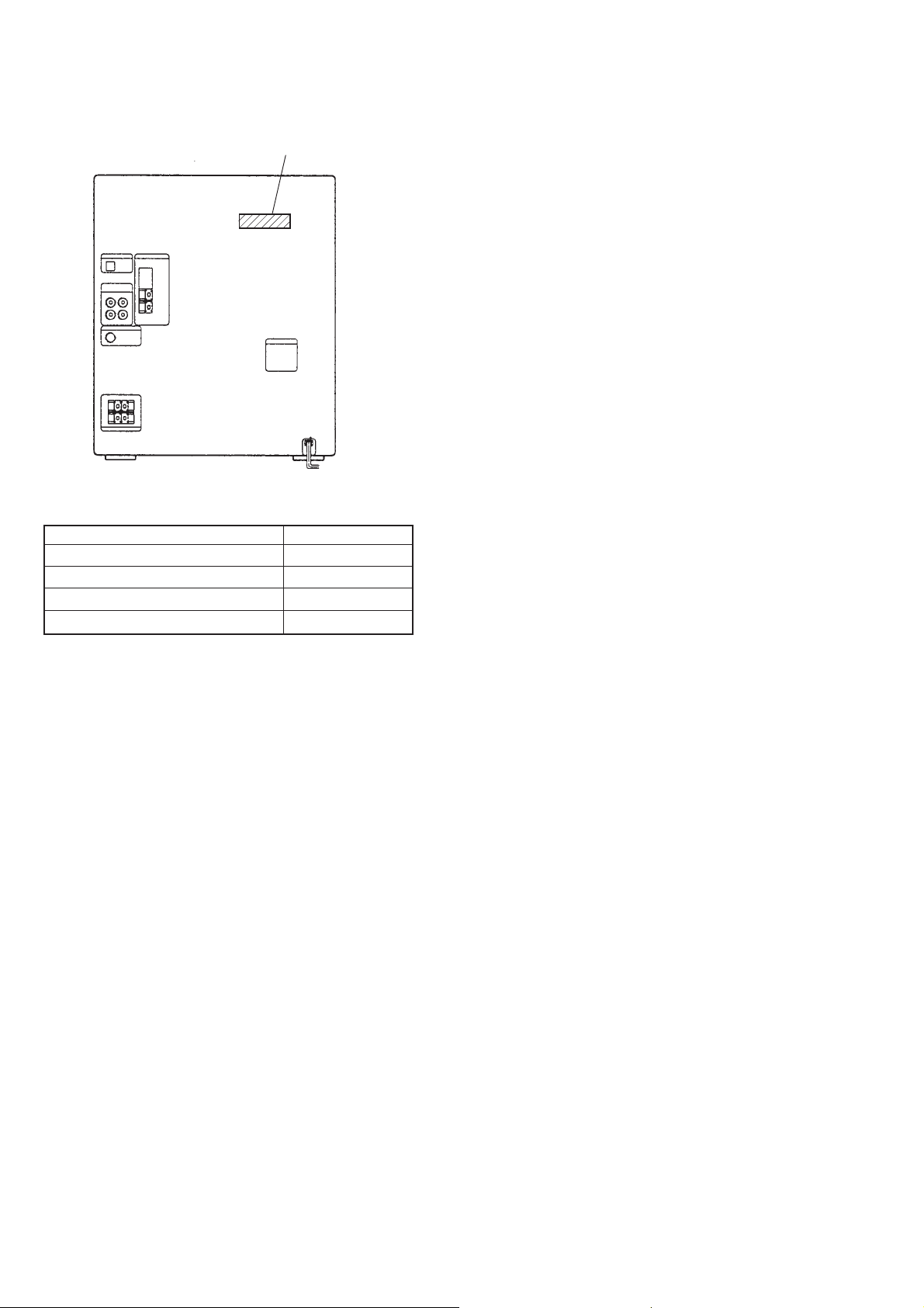
MODEL IDENTIFICATION
– Back Panel –
PART N o.
MODEL PART No.
E model 4-996-846-0π
Malaysia, Singapore models 4-996-846-1π
Saudi Arabia model 4-996-846-2π
East European, CIS models 4-996-846-5π
SAFETY-RELATED COMPONENT WARNING!!
COMPONENTS IDENTIFIED BY MARK ! OR DOTTED
LINE WITH MARK ! ON THE SCHEMATIC DIA GRAMS
AND IN THE PARTS LIST ARE CRITICAL TO SAFE
OPERATION. REPLACE THESE COMPONENTS WITH
SONY PARTS WHOSE PART NUMBERS APPEAR AS
SHOWN IN THIS MANUAL OR IN SUPPLEMENTS PUBLISHED BY SONY.
– 4 –
Page 5

HOW TO OPEN THE DISC TRAY WHEN POWER SWITCH TURNS OFF.
e
1
Remove the Case.
3
Pull-out the disc tray.
2
Turn the cam to the
direction of arrow.
NOTE FOR INSTALLATION (ROTARY ENCODER)
BU cam
Section A
Groove
Note:When attaching the BU cam,
engage the Rotary encoder
switch as shown in the figure.
Note:When attaching the Base unit, Insert th
section A into the groove of BU cam.
– 5 –
Page 6
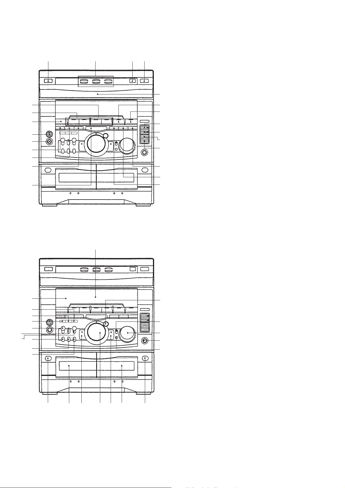
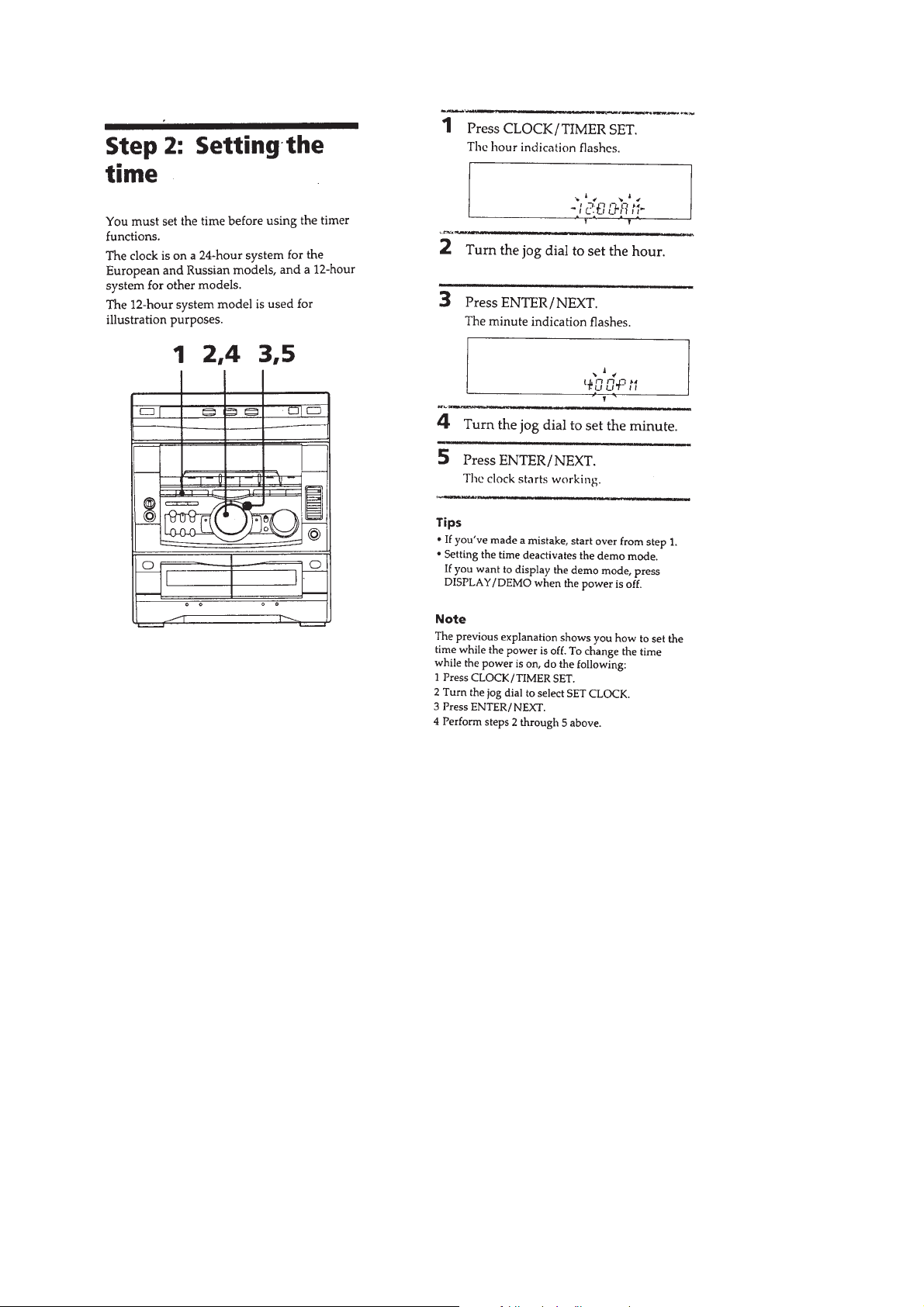
LOCATION OF CONTROLS
SECTION 2
GENERAL
!∞
!§
!¶
!•
!ª
@º
@¡
@™
@£
1 2 3 4
5
6
7
8
9
!º
!¡
!™
!£
!¢
1 I /u (Power) button
2 DISC 1 to 3 buttons and indicators
3 DISC SKIP/EX-CHANGE button
4 6 (CD) button
5 CD disc tray
6 CD ^ button and indicator
7 TUNER, BAND button
8 r REC button and indicator
9 P PAUSE button and indicator
!º HI-DUB button
!¡ CD SYNC button
!™ EFFECT button and indicator
!£ SURROUND button
!¢ KARAOKE PON/MPX button
!∞ TAPE B 9 and ( buttons and indicators
!§ TAPE A 9 and ( buttons and indicators
!¶ FUNCTION button
!• MIC LEVEL knob
!ª MIX MIC jac
@º DISPLAY/DEMO button
@¡ CLOCK/TIMER SET button
@™ TIMER SELECT button
@£ p button
#∞
#§
#º
#¡
#™
#£
#¢
#¶
#•
#ª
@¢
$º $¡ $™ $£ $¢ $∞ $§
@∞
@§
@¶
@•
@ª
@¢ Fluorescent indicator tube
@∞ ENTER/NEXT button and indicator
@§ GROOVE button and indicator
@¶ VOLUME konb
@• PHONES jack
@ª DBFB button
#º Remote sensor
#¡ P FILE MEMORY button
#™ GEQ CONTROL button
#£ FILE SELECT button
#¢ LOOP button
#∞ NON-STOP button and indicator
#§ FLASH button
#¶ EDIT, DIRECTION button
#• PLAY MODE, DOLBY NR button
#ª REPEAT button
$º § button (deck A)
$¡ Tape deck A
$™ –, 0 button and indicator
$£ JOG dial
$¢ +, ) button and indicator
$∞ Tape deck B
$§ § button (deck B)
– 6 –
Page 7
– 7 –
Page 8
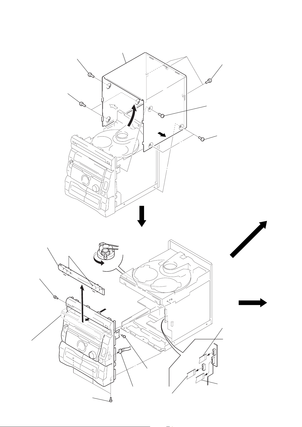
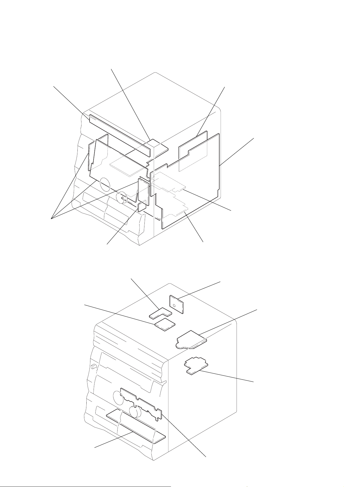
SECTION 3
)
DISASSEMBLY
Note: Follow the disassembly procedure in the numerical order given.
CASE
2
screw
(CASE3 TP2) (3 × 12)
3
two screws
(CASE3 TP2) (3 × 8)
4
6
case
5
4
1
three screws
(BVTT3 × 8)
2
screw
(CASE3 TP2) (3 × 12)
3
two screws
(CASE3 TP2) (3 × 8
FRONT PANEL SECTION
4
loading panel
3
two claws
9
screw
(BVTP3
2
Pull-out the
disc tray.
×
10)
1
Turn the cam to the direction
of arrow
A
A
.
9
screw
(BVTP3
×
10)
5
wire (flat type)
(15 core) (33 cm)
(CN106)
0
three screws
(BVTT3
7
wire (flat type)
8
connector
(CN109)
×
6)
6
wire (flat type) (13 core)
(23 cm) (CN201)
(17 core) (CN107)
– 8 –
Page 9
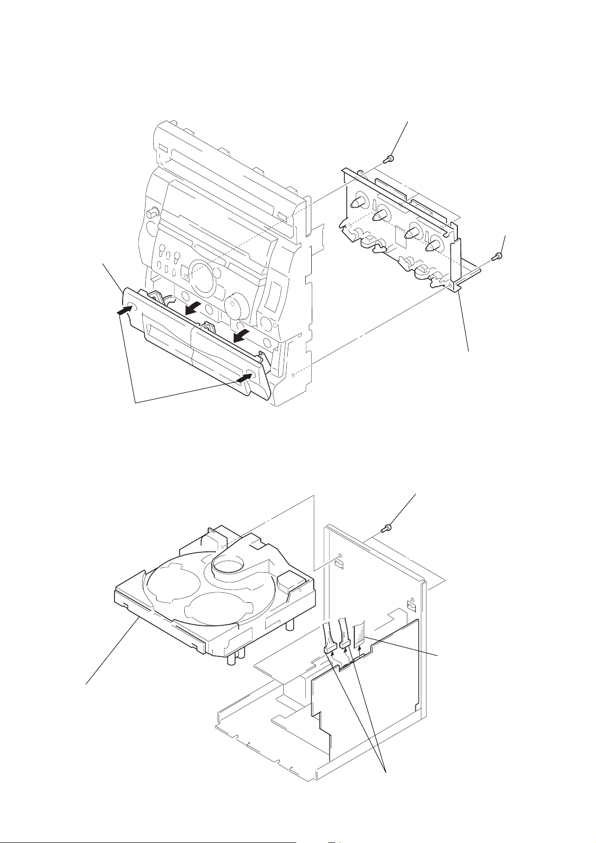
TAPE MECHANISM DECK SECTION (TCM-230AWR1/TCM-230PWR1)
1
Push the
cassette lids.
3
three screws
(BVTP3
×
8)
2
Open the
cassette lids.
4
two screws
(BVTP3
×
8 )
5
tape mechanism
deck section
(TCM-230AWR1/
TCM-230PWR1)
4
CD mechanism deck section
(CDM38LH-5BD29AL)
Note: The CD mechanism deck will
fall if two screws are removed.
Support it by hand, then remove
three screws.
3
two screws
(BVTP3
×
8)
2
wire (flat type) (19 core) (24 cm)
(CN105)
1
two connectors
(CN103, CN104)
CD MECHANISM DECK SECTION (CDM38LH-5BD29AL)
– 9 –
Page 10
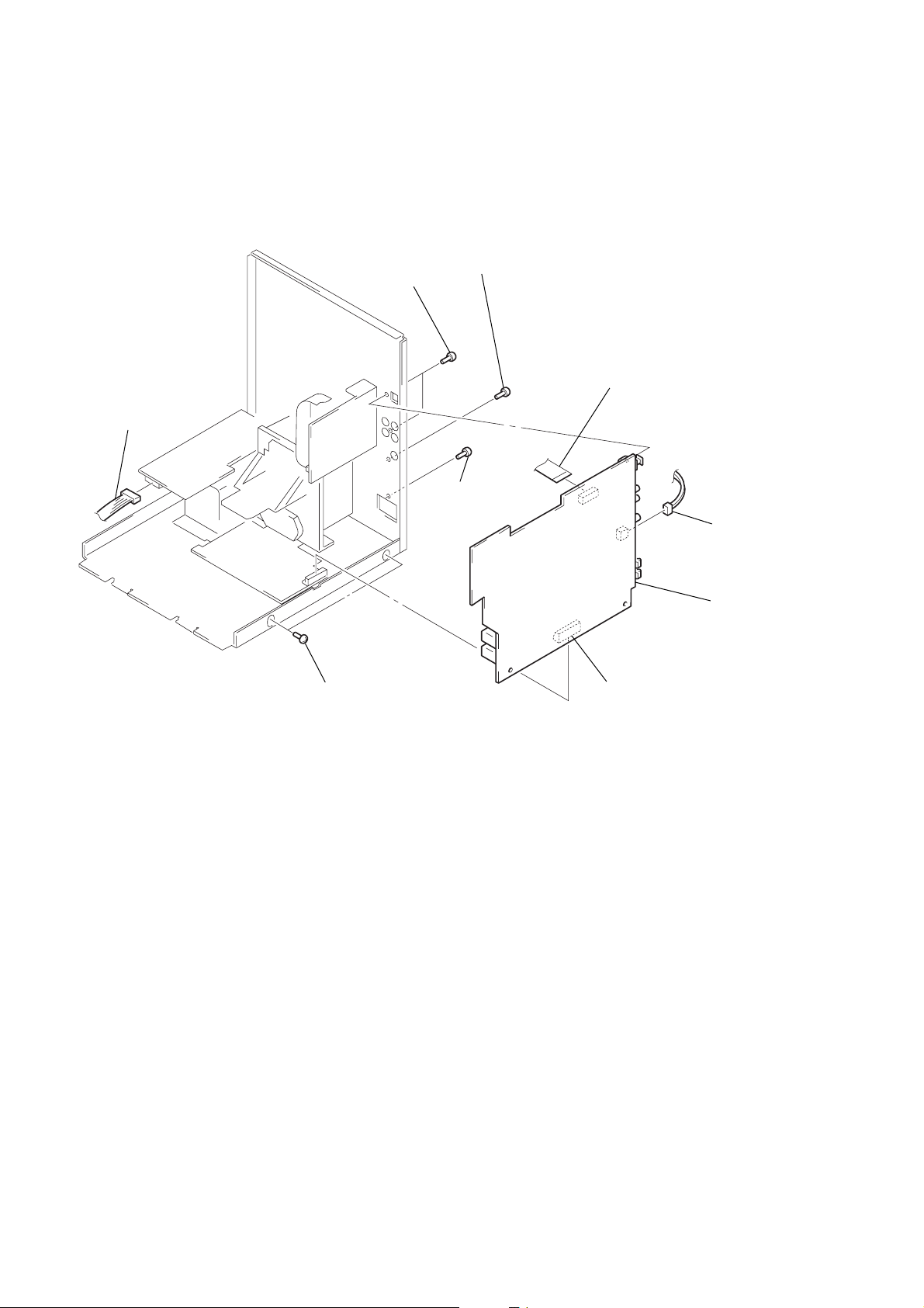
MAIN BOARD
d
1
connector
(CN11)
3
two screws
(BVTP3 × 8)
3
3
screw
(BVTP3 × 8)
screw
(BVTP3 × 8)
2
wire (flat type) (13 core) (14 cm)
(CN102) (E, Thai)
wire (flat type) (15 core) (14 cm)
(CN102) (EXCEPT E, Thai)
7
connector
(CN110)
4
two screws
(BVTT3 × 6)
5
connector
(CN101)
6
MAIN boar
– 10 –
Page 11

SECTION 4
TEST MODE
[MC Cold Reset]
• The cold reset clears all data including preset data stored in the
RAM to initial conditions. Execute this mode when returning
the set to the customer.
Procedure:
1. Press three buttons p , [ENTER/NEXT], and I/u simulta-
neously.
2. The fluorescent indicator tube becomes blank instantaneously ,
and the set is reset.
[CD Delivery Mode]
• This mode moves the pickup to the position durable to vibration. Use this mode when returning the set to the customer after
repair.
Procedure:
1. Press I/u button to turn the set ON.
2. Press [LOOP] button and I/u button simultaneously.
3. A message “LOCK” is displayed on the fluorescent indicator
tube, and the CD delivery mode is set.
[MC Hot Reset]
• This mode resets the set with the preset data kept stored in the
memory. The hot reset mode functions same as if the power
cord is plugged in and out.
Procedure:
1. Press three buttons p , [ENTER/NEXT], and [DISC1] si-
multaneously.
2. The fluorescent indicator tube becomes blank instantaneously ,
and the set is reset.
[Sled Servo Mode]
• This mode can run the CD sled motor freely. Use this mode, for
instance, when cleaning the pickup.
Procedure:
1. Press
2. Select the function “CD”.
3. Press three buttons p , [ENTER/NEXT], and § simulta-
4. The Sled Servo mode is selected, if “CD” is blanking on the
5. With the CD in stop status, press ) + button to move the
6. To exit from this mode, perform as follows:
Note: • Always move the pickup to most inside track when exiting from
I/u button to turn the set ON.
neously.
fluorescent indicator tube.
pickup to outside track, or – 0 button to inside track.
1) Move the pickup to the most inside track.
2) Press three buttons in the same manner as step 3.
this mode. Otherwise, a disc will not be unloaded.
• Do not run the sled motor excessively , otherwise the gear can be
chipped.
[Change-over of AM Tuner Step between 9 kHz and
10 kHz]
• A step of AM channels can be changed ov er between 9 kHz and
10 kHz.
Procedure:
1. Press I/u button to turn the set ON.
2. Select the function “TUNER”, and press [TUNER/BAND]
button to select the BAND “AM”.
3. Press I/u button to turn the set OFF.
4. Press [ENTER/NEXT] and I/u buttons simultaneously, and
the display of fluorescent indicator tube changes to “AM 9 k
STEP” or “AM 10 k STEP”, and thus the channel step is
changed over.
[Change-over of LW Tuner Step between 1 kHz and
3 kHz]
• A step of L W channels can be changed ov er between 1 kHz and
3 kHz.
Procedure:
1. Press I/u button to turn the set ON.
2. Select the function “TUNER”, and press [TUNER/BAND]
button to select the BAND “LW”.
3. Press I/u button to turn the set OFF.
4. Press [ENTER/NEXT] and I/u buttons simultaneously, and
the display of fluorescent indicator tube changes to “LW 1 k
STEP” or “LW 3 k STEP”, and thus the channel step is changed
over.
[LED and Fluorescent Indicator Tube All Lit, Key Check
Mode]
Procedure:
1. Press three buttons p , [ENTER/NEXT], and [DISC2] si-
multaneously.
2. LEDs and fluorescent indicator tube are all turned on.
Press [DISC2] button, and the key check mode is activated.
3. In the key check mode, the fluorescent indicator tube displays
“K 1 J0 V0”. Each time a button is pressed, “K” value increases. However , once a button is pressed , it is no longer taken
into account.
“J” value increases like 1, 2, 3 ... if rotating [JOG] knob in “+”
direction, or it decreases like 0, 9, 8 ... if rotating in “–” direction.
“V” value increases like 1, 2, 3 ... if rotating [VOLUME] knob
in “+” direction, or it decreases like 0, 9, 8 ... if rotating in
“–” direction.
4. To exit from this mode, press three buttons in the same man-
ner as step 1, or disconnect the power cord.
[Change-over of FUNCTION Name]
• The FUNCTION name of external input terminal can be changed
over to “VIDEO” of “MD”.
Procedure:
1. Press I/u button to turn the set OFF.
2. Press I/u button together with [FUNCTION] button, and the
power is turned on, the display of fluorescent indicator tube
changes to “MD” of “VIDEO” instantaneously, and thus the
FUNCTION is changed over.
– 11 –
Page 12
[Aging Mode]
This mode can be used for operation check of CD section and tape
deck section.
• If an error occurred:
The aging operation stops and display status.
• If no error occurs:
The aging operation continues repeatedly.
1. Operating Method of Aging Mode
1) Set disc in DISC1 tray.
2) Load the tapes recording use into the decks A and B respec-
tively.
3) Press three buttons p , [ENTER/NEXT],
and [DISCSKIP/EX-CHANGE] simultaneously.
4) The aging mode is activated, if a CD roulette mark on the fluo-
rescent indicator tube is blinking.
5) To exit from the aging mode, press I/u button to turn the set
OFF.
2. Operation Sequence
• During the aging mode in the following sequence to below.
• Starting the CD section aging for function set “CD”, starting
the TAPE section (deck A) aging for function set “TAPE A” or
“TAPE B”. (Set another function is no work.)
CD (disc1) (12 minutes) → Deck A
↑↓(Maximum about
Deck B 12 minutes)
3. Aging mode in CD section
1) Display state
• No error occurs
display
1 –
[*][*]
Note:
: a letter “CD” and the remainder time (minute) alternately. (re-
[*][*]
mainder time start from 12 minute)
@@: track number in access.
@ @
• Error occurred
NO. Display Main factor
1 NO DISC ERR Not set disc in DISC1
2 FOCUS1 ERR Focus does not work
3 FOCUS2 ERR Focus does not work after the disc rotate as usual
4 GFS ERR GFS error
5 FBIAS ERR Error in to the focus bias adjustment
6 SENSOR ERR Disc sensor sens DISC1 is no disc
7 TABLE ERR CD tray lotate does not work
8 TRAY ERR Tray (include BD) move does not work
4. Aging mode in Tape Deck section
1) Display state
• No error occurs
Display action now
• Error occurred
Display action last time
NO. Display action Action contents Final timing
1 TAPE A AG-1 Rewind the TAPE A The top of tape
2 TAPE A AG-2 FWD play the TAPE A 2 minutes playing
3 TAPE A AG-3 F.F. the TAPE A First either 20 seconds
or the end of tape
4 TAPE A AG-4 REV play the TAPE A 2 minutes playing
5 TAPE A AG-5 Rewind the TAPE A The top of tape
6 TAPE B AG-1 Rewind the TAPE B The top of tape
7 TAPE B AG-2 FWD play the TAPE B 2 minutes playing
8 TAPE B AG-3 F.F. the TAPE B First either 20 seconds
or the end of tape
9 TAPE B AG-4 REV play the TAPE B 2 minutes playing
10 TAPE B AG-5 Rewind the TAPE B The top of tape
2) Operation during Aging Mode
In the aging mode, the program is executed in the following sequence.
(1) The tape in deck A is rewound to the head.
(2) The FWD side is played back for 2 minutes.
(3) The tape is fast forwarded (FF) for 20 seconds. The follow-
ing procedure is performed when the tape end is reached
before the 20 seconds.
(4) The REV side is played back for 2 minutes.
(5) The tape is rewound to the head (REW).
(6) The tape in deck B is rewound to the head.
(7) The FWD side is played back for 2 minutes.
(8) The tape is fast forwarded (FF) for 20 seconds. The follow-
ing procedure is performed when the tape end is reached
before the 20 seconds.
(9) The REV side is played back for 2 minutes.
(10) The tape is rewound to the head (REW).
(11) Aging is switched to the CD player.
2) Operation during aging Mode
In the aging mode, the program is executed in the following sequence.
(1) The CD tray rotates and disc 1 is selected.
(2) Chucking is performed.
(3) TOC is read.
(4) Track 1 played back for 8 seconds.
(5) The CD tray opens and closes again.
(6) 1 to 5 is repeated.
(7) After 12 minutes of aging, aging is switched to the tape deck.
– 12 –
Page 13
SECTION 5
MECHANICAL ADJUSTMENTS
SECTION 6
ELECTRICAL ADJUSTMENTS
Precaution
1. Clean the following parts with a denatured alcohol-moistened
swab:
record/playback heads pinch rollers
erase head rubber belts
capstan idlers
2. Demagnetize the record/playback head with a head demagnetizer.
3. Do not use a magnetized screwdriver for the adjustments.
4. After the adjustments, apply suitable locking compound to the
parts adjusted.
5. The adjustments should be performed with the rated power
supply voltage unless otherwise noted.
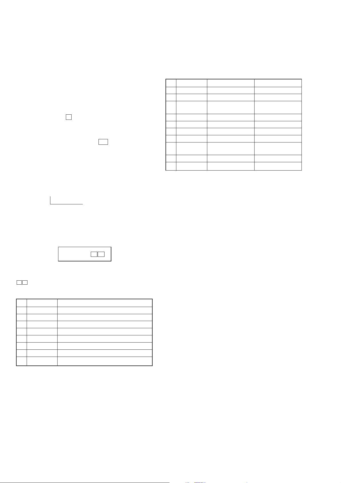
Torque Measurement
Mode Torque meter Meter reading
FWD CQ-102C
FWD
back tension (0.03 – 0.08 oz • inch)
REV CQ-102RC
REV
back tension (0.03 – 0.08 oz • inch)
FF/REW CQ-201B
FWD tension CQ-403A
REV tension CQ-403R
CQ-102C
CQ-102RC
31 to 71 g • cm
(0.43 – 0.98 oz • inch)
2 to 6 g • cm
31 to 71 g • cm
(0.43 – 0.98 oz • inch)
2 to 6 g • cm
71 to 143 g • cm
(0.99 – 1.99 oz • inch)
100 g or more
(3.53 oz or more)
100 g or more
(3.53 oz or more)
DECK SECTION 0 dB=0.775 V
1. Demagnetize the record/playback head with a head demagnetizer.
2. Do not use a magnetized screwdriver for the adjustments.
3. After the adjustments, apply suitable locking compound to the
parts adjust.
4. The adjustments should be performed with the rated power
supply voltage unless otherwise noted.
5. The adjustments should be performed in the order given in
this service manual. (As a general rule, playback circuit adjustment should be completed before performing recording
circuit adjustment.)
6. The adjustments should be performed for both L-CH and RCH.
7. Switches and controls should be set as follows unless otherwise specified.
• Test Tape
Tape Signal Used for
P-4-A100 10 kHz, –10 dB Azimuth Adjustment
WS-48B 3 kHz, 0 dB Tape Speed Adjustment
P-4-L300 315 Hz, 0 dB Level Adjustment
Record/Playback Head Azimuth Adjustment
DECK A DECK B
Note: Perform this adjustments for both decks
Procedure:
1. Mode: Playback (FWD)
test tape
P-4-A100
(10 kHz, –10 dB)
set
MAIN board
CN301
3
(L-CH)
Pin
Pin
1
(R-CH)
MAIN board
CN301
Pin
2
(GND)
level meter
+
–
– 13 –
Page 14
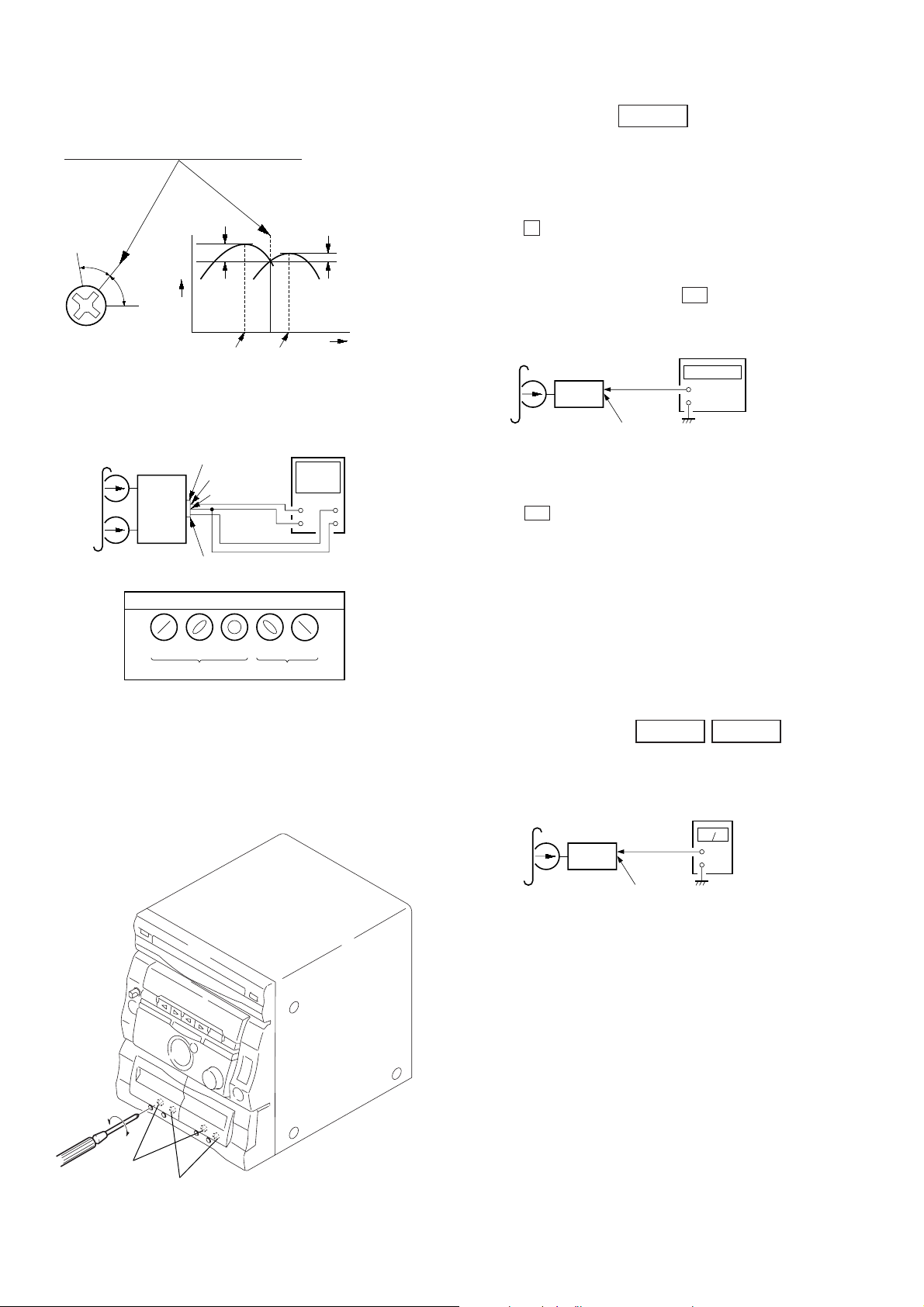
2. Turn the adjustment screw and check output peaks. If the peaks
(
)
do not match for L-CH and R-CH, turn the adjustment screw
so that outputs match within 1dB of peak.
Output
level
within
1dB
L-CH
peak
R-CH
peak
within
1dB
Screw
position
L-CH
peak
Screw
position
R-CH
peak
3. Mode: Playback (FWD)
Tape Speed Adjustment DECK B
Note: Start the Tape Speed adjustment as below after setting to the test
mode.
In the test mode, the tape speed is high during pressing the
[HI-DUB] button.
Procedure:
1. Turn the power switch on.
2. Press the p button, [ENTER/NEXT] button and [DISC3] b utton
simultaneously.
(The “VOLUME” on the fluorescent indicator tube will blink
while in the test mode.)
To exit from the test mode, press the I/u button.
Mode: Playback
test tape
WS-48B
(3 kHz, 0 dB)
set
frequency counter
+
–
test tape
P-4-A100
(10 kHz, –10 dB)
in phase 45 °90 °135 °180
MAIN board
CN301
(pin
3
: L-CH)
(pin
good
(pin 2: GND)
1
: R-CH)
wrong
set
waveform of oscilloscope
oscilloscope
H
V
°
4. Repeat setps 1 to 3 in playback (REV) mode.
5. After the adjustments, apply suitable locking compound to the
pats adjusted.
Adjustment Location:Playback Head (Deck A).
Record/Playback/Erase Head (Deck B).
MAIN board
CN301 (Pin
3
: L-CH)
Pin 1 : R-CH
1. Insert the WS-48B into the deck B.
2. Press the · button on the deck B.
3. Press the [HI-DUB] button in playback mode.
Then at HIGH speed mode.
4. Adjust RV1001 on the LEAF SW board do that frequency
counter reads 6,000 ± 180 Hz.
5. Press the [HI-DUB] button.
Then back to NORMAL speed mode.
6. Adjust RV1002 on the LEAF SW board so that frequency
counter reads 3,000 ± 90 Hz.
Adjustment Location: LEAF SW board
Sample value of Wow and Flutter: 0.3% or less W.RMS (JIS)
(WS-48B)
Playback level Adjustment DECK A DECK B
Procedure:
Mode: Playback
test tape
P-4-L300
(315 Hz, 0 dB)
set
level meter
+
–
forward
reverse
MAIN board
CN301 (Pin
(Pin
3
1
: L-CH)
: R-CH)
Deck A is RV311 (L-CH) and RV411 (R-CH), Deck B is RV301
(L-CH) and RV401 (R-CH) so that adjustment within adjustment
level as follows.
Adjustment Level:
CN301 PB level: 301.5 to 338.3 mV (–8.2 to –7.2 dB) level
difference between the channels: within ± 0.5 dB
Adjustment Location: AUDIO board
– 14 –
Page 15
REC Bias Adjustment DECK B
set
MD/VIDEO (AUDIO) IN
315 Hz, 50 mV (–23.8 dB)
blank tape
CS-123
600
Ω
attenuator
AF OSC
+
–
++
–
–
+
–
set
recorded
portion
MAIN board
CN301 (Pin
3
: L-CH)
(Pin
1
: R-CH)
level meter
REC LEVEL
13
RV301
L
RV351
R
CN106
CN301
CN107
RV401
RV301
RV341
RV311
RV411
IC602
CN601
LR
RL
RV441
PB LEVEL
– DECK B –
REC BIAS
LR
PB LEVEL
– DECK A –
Procedure:
INTRODUCTION
When set to the test mode performed in T ape Speed Adjustment,
when the tape is rewound after recording, the “REC memory mode”
which rewinds only the recorded portion and playback is set.
This “REC memory mode” is convenient for performing this adjustment. During recording, the input signal FUNCTION will automatically switch to VIDEO.
(After recording, press the – 0 button without stopping will
return to the position where recording was started.)
1. Press [FUNCTION] button to select VIDEO. (This step is not
necessary if the above test mode has already been set.)
2. Insert a tape into deck B.
3. After press [REC] button, press P button, then recording
r
start.
4. Mode: Record
4. Mode: Record
5. Mode: Playback
AF OSC
+
–
MD/VIDEO (AUDIO) IN
1) 315 Hz
2) 10 kHz
attenuator
+
–
50 mV (–23.8 dB)
600
Ω
+
–
set
blank tape
CN-123
5. Mode: Playback
recorded
portion
set
MAIN board
CN301 (Pin
(Pin
level meter
+
–
3
: L-CH)
1
: R-CH)
6. Confirm playback the signal recorded in step 3 become adjustable level as follows.
If these levels do not adjustable level, adjustment the RV341
(L-CH) and RV441 (R-CH) on the AUDIO board to repeat
steps 4 and 5.
Adjustable level: Playback output of 315 Hz to playback output
of 10 kHz: ± 1.0 dB
Adjustment Location: AUDIO board
6. Confirm playback the signal recorded in step 3 become adjustable level as follows.
If these levels do not adjustable level, adjustment the RV301
(L-CH) and R V351 (R-CH) on the MAIN board to repeat steps
4 and 5.
Adjustable level:
CN301 PB level: 47.2 to 53.0 mV (–24.3 to –23.3 dB)
Adjustment Location: MAIN board
Adjustment Location:
[MAIN BOARD] (Component Side)
REC Level Adjustment DECK B
Procedure:
INTRODUCTION
When set to the test mode performed in T ape Speed Adjustment,
when the tape is rewound after recording, the “REC memory mode”
which rewinds only the recorded portion and playback is set.
This “REC memory mode” is convenient for performing this adjustment. During recording, the input signal FUNCTION will automatically switch to VIDEO.
(After recording, press the – 0 button without stopping will
return to the position where recording was started.)
1. Press [FUNCTION] button to select VIDEO. (This step is not
necessary if the above test mode has already been set.)
2. Insert a tape into deck B.
3. After press [REC] button, press P button, then recording
start.
r
[AUDIO BOARD] (Component Side)
[LEAF SW BOARD] (Component Side)
TAPE SPEED
(NORMAL) (HIGH)
RV1002
RV1001
– 15 –
CN1001
Page 16
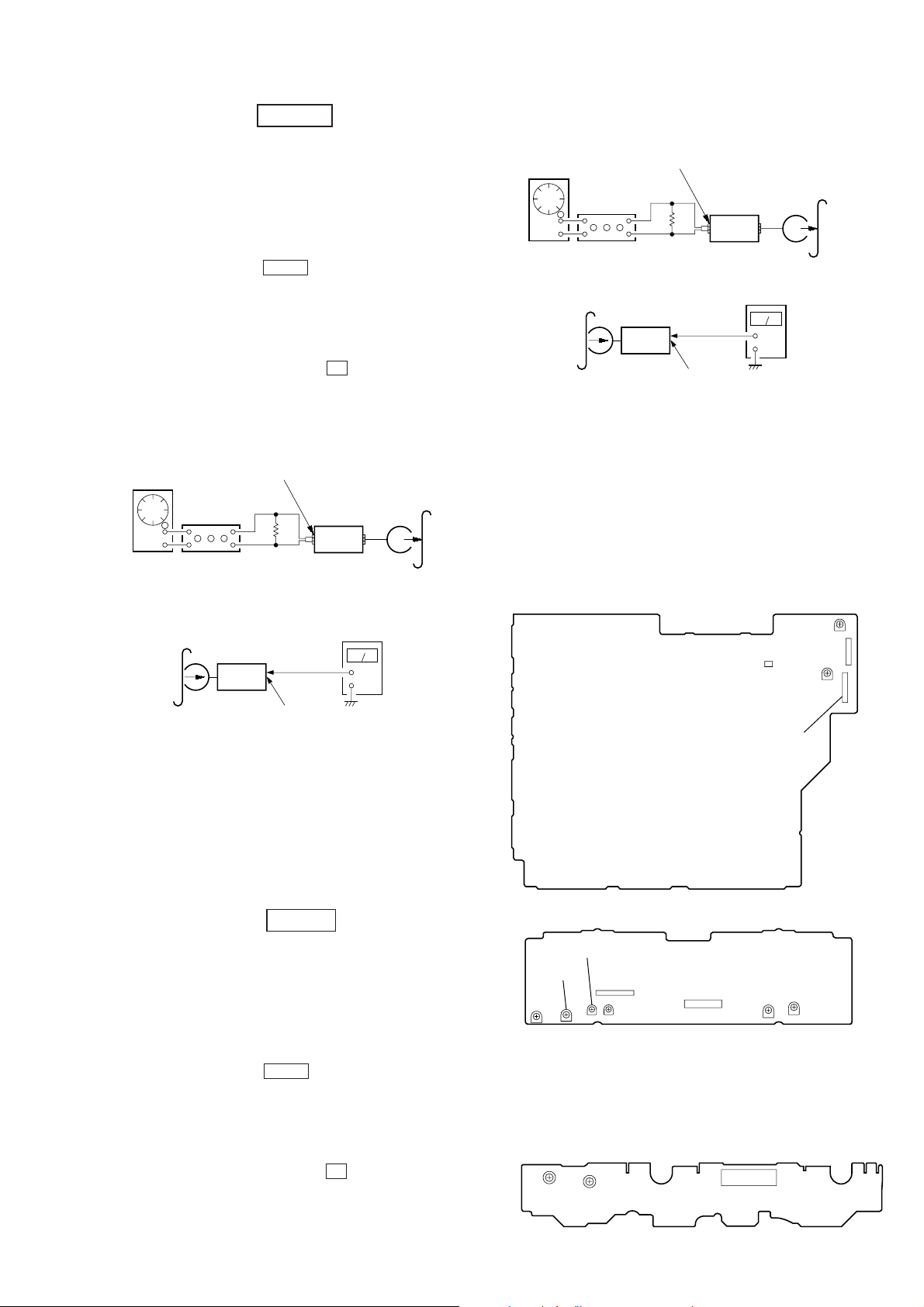
TUNER SECTION 0 dB=1 µV
l
(East European, CIS models only)
Note: As a front-end (FE1) is difficult to repair if faulty, replace it with
new one.
MW Section Adjustment
Note: FM Tuned Level Adjustment should be performed after this MW
Tuned Level Adjustment.
Setting:
loop antenna
AM RF SSG
30% amplitude
modulation by
400 Hz signal
Field strength dB (
60 cm
MW Tuned Level Adjustment
Band: MW
Procedure:
1. Set the output of SSG so that the input level of the set becomes 55 dB.
2. Tune the set to 1,050 kHz.
3. Adjust R V41 to the point (moment) when the TUNED indicator will change from going off to going on.
Adjustment Location : TCB board
loop antenna
(Supplied accessories)
µ
V/m) =SSG output level dB (µV/m) –26 dB.
set
MW ANTENNA
terminal (TM1)
FM Section Adjustment
Note: This adjustment should be performed after the MW Tuned Level
Adjustment due to the same adjustment element.
Setting:
FM RF stereo signal
generator
Ω
coaxial
75
set
Carrier frequency : 98 MHz
Modulation : AUDIO 1 kHz, 75 kHz
deviation (100%)
FM ANTENNA termina
(TM1) (75 Ω open)
FM Tuned Level Adjustment
Band: FM
Procedure:
1. Supply a 25 dBµ 98 MHz signal from the ANTENNA terminal.
2. Tune the set to 98 MHz.
3. If the TUNED indicator does not light, adjust RV42 to the
point (moment) when the TUNED indicator will change from
going off to going on.
Adjustment Location: TCB board
– 16 –
Page 17
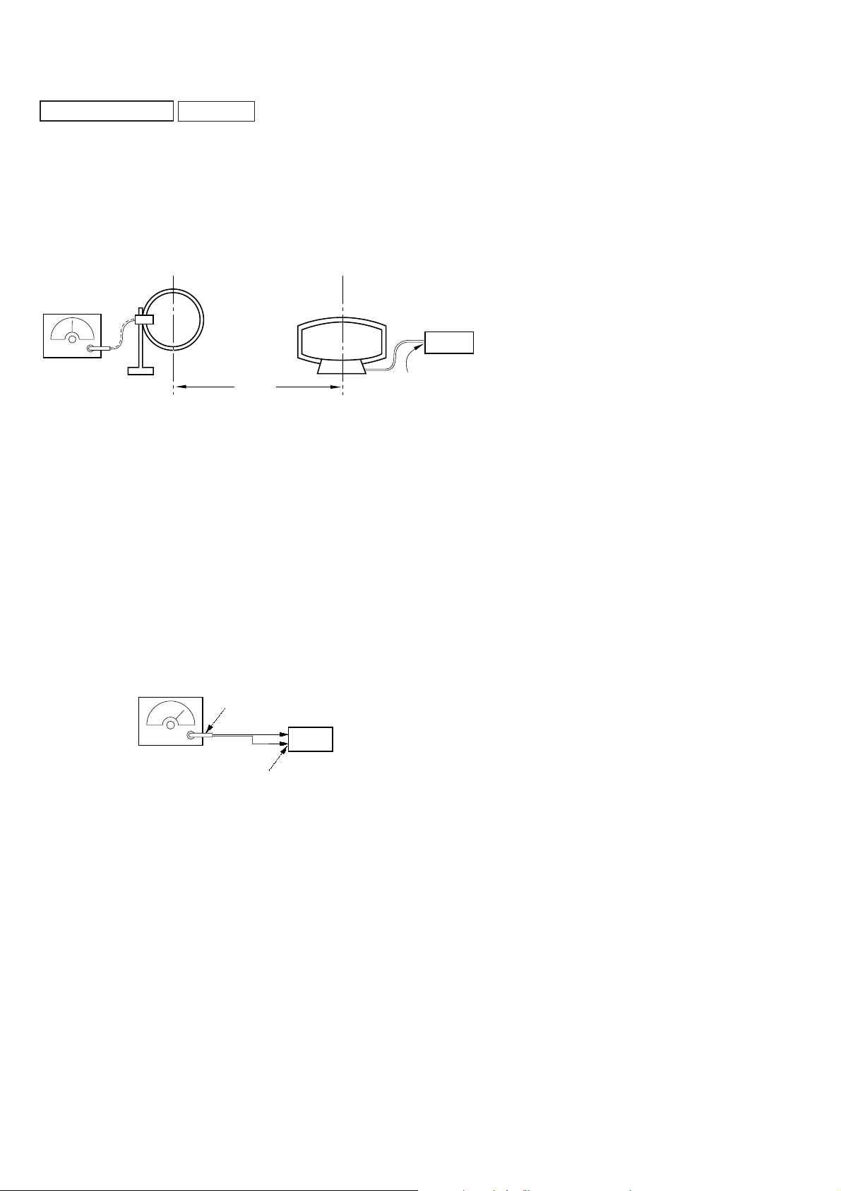
FM Polar Adjustment
l
)
k
frequency
counter
+
–
+
–
level meter
Q1701
Q1702
Q1703
TP1701
(FILTER)
TP1702
(VCO)
Connection 1:
FM RF SSG
Ω
coaxial
75
set
FM ANTENNA termina
(75 Ω)
Carrier frequency: 69 MHz
Output level : 1mV (60dB
Modulation : AUDIO 1 kHz, 10kHz deviation
µ
) (at 75 Ω open)
Connection 2:
AF OSC
FM RF SSG
75 Ω coaxial
Audio 31.25 kHz
Carrier frequency: 69 MHz
Output level : 1mV (60 dBµ) (at 75 Ω open)
Modulation : AUDIO 31.25 kHz, 10 kHz deviation
external
modulation
terminal
(EXTERNAL MODULATION
FM ANTENNA terminal
(75 Ω)
Procedure :
1. Set the modulation of FM RF SSG to AUDIO 1 kHz, 10 kHz
deviation according to “Connection 1”.
2. Tune the set to 69 MHz.
3. Adjust the RV1702 so that the reading of frequency counter
connected to TP1702 becomes within 31.25 kHz ± 0.05 kHz.
(VCO Adjustment)
4. Then record the reading of the level meter connected to TP1701
5. Set the modulation of FM RF SSG to AUDIO 31.25 kHz, 10
kHz deviation according to “Connection 2”.
6. Tune the set to 69 MHz.
7. Set the CT1701 to be mechanical center.
8. Adjust the L1701 so that the reading of the level meter connected to TP1701 become maximum.
Then adjust the CT1701 so that the reading of the level meter
connected to TP1701 becomes maximum. (SUB CARRIER
PEAK Adjustment)
9. Adjust the RV1701 so that the level at the moment becomes
14dB higher value than the level recorded in step 4. (SUB CARRIER LEVEL Adjustment)
set
Adjustment Location :
[TCB BOARD] (Component Side)
TM1
IFT41
IC41
CN1
RV41
MW T uned Level
Adjustment
RV42
FM T uned Level
Adjustment
L1701
Sub Carrier Pea
Adjustment
RV1701
Sub Carrier Level
Adjustment
CT1701
Sub Carrier Peak
Adjustment
RV1702
VCO Adjustment
[TCB BOARD] (Conductor Side)
– 17 –
Page 18

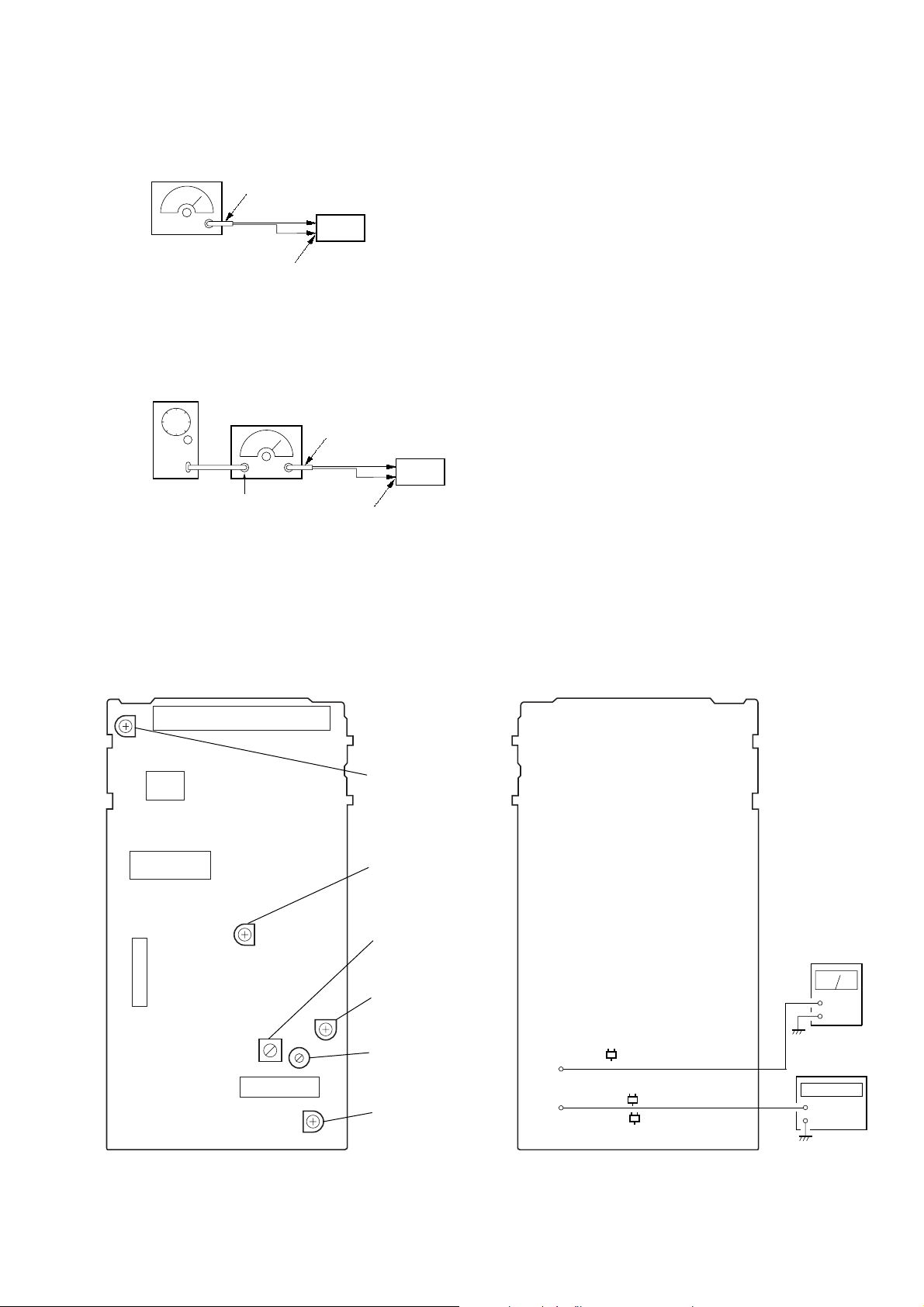
CD SECTION
V
+
–
BD board
TP (TEO)
TP (VC)
oscilloscope
)
Note:
1. CD Block is basically designed to operate without adjustment. Therefore, check each item in order given.
2. Use YEDS-18 disc (3-702-101-01) unless otherwise indicated.
3. Use an oscilloscope with more than 10 MΩ impedance.
4. Clean the object lens by an applicator with neutral detergent when the
signal level is low than specified value with the following checks.
E-F Balance (Traverse) check
(Without remote commander)
S Curve Check
oscilloscope
BD board
TP (FEO)
TP (VC)
+
–
Procedure:
1. Connect oscilloscope to test point TP (FEO).
2. Connect between test point TP (FOK) and GND by lead wire.
3. Turn Power switch on.
4. Put disc (YEDS-18) in and turned Power switch on again and
actuate the focus search. (Actuate the focus search when disc
table is moving in and out.)
5. Check the oscilloscope waveform (S-curve) is symmetrical
between A and B. And confirm peak to peak level within 3±1
Vp-p.
S-curve waveform
symmetry
A
B
within 3
±
1 Vp-p
6. After check, remove the lead wire connected in step 2.
Note: • T ry to measure se v eral times to make sure than the ratio of A : B
or B : A is more than 10 : 7.
• Take sweep time as long as possible and light up the brightness
to obtain best waveform.
RF Level Check
oscilloscope
BD board
TP (RF)
TP (VC)
+
–
Procedure:
1. Connect oscilloscope to test point TP (RF) on BD board.
2. Turned Power switch on.
3. Put disc (YEDS-18) in and playback.
4. Confirm that oscilloscope waveform is clear and check RF signal level is correct or not.
Note: Clear RF signal waveform means that the shape “≈” can be clearly
distinguished at the center of the waveform.
Procedure:
1. Connect oscilloscope to test point TP (TEO) on BD board.
2. Turned Power switch on. Press [FUNCTION] button to select
CD.
3. Put disc (YEDS-18) in to play the number five track.
4. Press the p button, [ENTER/NEXT] button and ^ button simultaneously several times to fluorescent indicator tube
display “SHUFFLE” is blink. (The sledding servo is turned
OFF.)
5. Check the level B of the oscilloscope’s waveform and the A
(DC voltage) of the center of the Traverse waveform.
Confirm the following:
A
× 100 = less than ±7 (%)
B
Traverse waveform
0 V
level: 500
±
100 mVp-p
Center of the waveform
B
A (DC
voltage)
symmetry
6. Press the p button, [ENTER/NEXT] button and ^ button
simultaneously several times to fluorescent indicator tube display “SHUFFLE” is OFF. (The sleding servo is turned ON.)
Confirm the C (DC voltage) is almost equal to the A (DC v oltage) is step 5.
Traverse waveform
0 V
Sled servo ONSled servo OFF
C (DC
voltage
• FR signal
VOLT/DIV: 200 m
TIME/DIV: 500 ns
level:
±
1.3
0.3 Vp-p
– 18 –
Page 19
Adjustment Location:
[BD BOARD] (Conductor Side)
CNU101
GND
TEO
IC103
CNU102
FEO
RF
IC101
FOK
VC
IC
I02
– 19 –
Page 20
• Circuit Boards Location
SECTION 7
DIAGRAMS
CD-SW board
PANEL board
TRANSFORMER board
TCB board
(East European, CIS)
TUNER (FM / AM)
(E, Saudi Arabia, Singapore, Malaysia)
MAIN board
AMP (R) board
CONNECTOR board
HP board
SENSOR board
AMP (L) board
MOTOR (TURN) board
BD board
MOTOR (SLIDE) board
AUDIO board
LEAF SW board
– 20 –
Page 21
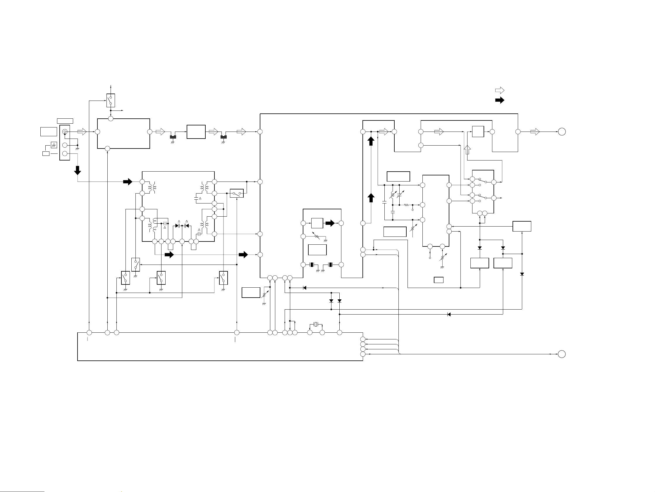
7-1. BLOCK DIAGRAM – TUNER Section (East European, CIS models only) –
HCD-GRX9000/RX900
FM 75Ω
COAXIAL
AM
TM1
ANTENNA
ST +10V
• SIGNAL PATH
: FM
Q5
B+ SWITCH
FM CIRCUIT B+
5
+B
8
ANT IN
FM FRONT-END
VT
4
Q13
MW
SWITCH
FE1
IF OUT
6
5
3
2
1
26 252423
Q14
LW SWITCH
CF1
10.7MHz
MW/LW FRONT-END
Q12
MW
SWITCH
FE2
22
FM IF AMP
21
Q1 – 4
20
SWITCH
Q11
MW
12
13
14
15
16
17
CF3
10.7MHz
Q9
LW SWITCH
RV42
FM TUNED
LEVEL
1
28
29
27
FM-IN
REG
AM-OSC
AM-RF IN
FM SD
30
VCO-STOP
AM/FM
14 15 13
AM-MIX
AM-SD
ADJ
AM
SD
IF-BUFF MUTE
FM/AM IF AMP,
AM RF AMP/MIX/OSC,
FM/AM DET, MPX
IC41
AM IF
2
IFT41
12
RV41
AM TUNED
LEVEL
10
X42
450kHz
D41
10.7MHz
D42
X41
FM DET-OUT
AM
AM
4
DET
IF
OUT
STEREO
TUNED
FM DET
9
D43
MPX
OUT L
23
24
7
6
22
IN
CT1701, L1701, TP1701
SUB CARRIER
PEAK
L1701
TP1701
RV1701
SUB CARRIER
LEVEL
STEREO
TUNED
MUTE
OUT R
CT1701
21
20
POLAR DECODER
IC1701
IN
2
SUB IN
3
SUB IN
20
VCO STOP
MON
18
TP1702
TP1702, RV1702
L OUT
R OUT
ST IND
VCO
7
6
9
10
VCO
17
RV1702
LPF41
L.P.F.
POLAR /PILOT SWITCH
IC1702
12
13
5
3
CA
11
9
D1701
SWITCHING
Q1702
AMP
19
IN L
14
4
D1702
SWITCHING
Q1703
: AM (MW/LW)
AMP
17
OUT L
R-CH
SWITCHING
Q1701
D1703
ST-L
A
(Page 27)
X21
4.5MHz
10
FM
05
9 11
17
VT1
MW
FM/AM PLL
IC21
MW
14
AM OSC
12
2
7
FM
FM/AM IF
VCO STOP
8
IF REQ
1
24
XIN
XOUT
13
FM LOW
CE
DI
CL
DO
ST-CE
3
ST-DOUT
4
ST-CLK
5
ST-DIN
6
D1704
STEREO, TUNED, ST-MUTE,
ST-CE, ST-DOUT, ST-CLK, ST-DIN
B
(Page 27)
– 21 – – 22 –
Page 22
HCD-GRX9000/RX900
7-2. BLOCK DIAGRAM – CD Section –
PD1 I-V AMP
PD1
38
PD2 I-V AMP
PD2
39
AUTOMATIC
POWER CONTROL
Q101
F
41
E
42
LD
36
DETECTOR
A
D
B
C
F
E
OPTICAL PICK-UP
(KSS-213D/Q-NP)
LASER DIODE
PD
4
5
1
2
I-V AMP
10
6
LD
RF
+
SUMMING
AMP
RF AMP,
FOCUS/TRACKING
SERVO
IC101 (1/2)
I-V
AMP
LD
AMP
PD
AMP
FOCUS
ERROR
AMP
TRACKING
ERROR
AMP
PD
37
RFO
33
RFI
32
FOCUS OK
COMPARATOR
MIRR
AMP
DEFECT
AMP
FEO
FE BIAS
TEO
DIGITAL SIGNAL PROCESSOR,
CLV SERVO PROCESSOR,
DIGITAL FILTER, D/A CONVERTER
FOK
DATA
CLK
XLT
LOCK
XRST
SENS1
C.OUT
SENS2
FEO
TAO
27
22
20
21
19
23
25
24
26
6
13
73
FOCUS OK
AMP
TTL
IIL
1
40
45
FEI
2
TEI
47
TTL
IIL
IIL
IIL DATA REGISTER
TTL
FOCUS PHASE
COMPENSATION
TRACKING PHASE
COMPENSATION
IC103
RF
ASYI
ASYO
FOK
DATO
CLKO
XLTO
SEIN
CNIN
ASYMMETRY
CORRECTION
XRST
100
57
XRST
SQ-DATA-IN
CD-DATA
SERVO AUTO SEQUENCER
SYSTEM CONTROLLER
SENS
CD-CLK
XLT
SCOR
44
46
47
23
15
17
16
13
14
SQ-CLK (D-OUT ON/OFF)
SENS2
DIGITAL CLV
MON
26
IC501 (1/3)
34
36
74
47
48
58
18
FILTER
39
42
FILO
CLTV
DIGITAL PLL
XROF
MDS29LOCK64SQSO
MDP
28
27
PCO
4038
FILI
SQCK
8 7
EFM
DEMODULATOR
SUB-CODE
PROCESSOR
CPU INTERFACE
SENS
XLAT
CLOK
DATA
91012
117576
INTERNAL BUS
ERROR
CORRECTOR
CKO
SPOD
SCOR
SBSO
EXCK
77
6
21
S101
(LIMIT)
ON : When the optical pick-up
is inner position.
D/A
16K
RAM
TIMING
LOGIC
XTAI
89
16.9344MHz
INTERFACE
WDCK
DIGITAL
XTAO70C4M
90
X101
PCMD
BCK
LRCK
C2PO
RFCK
OUT
GENERATOR
52
54
50
63
62
49
DOUT
EMPH
WFCK
CLOCK
GFS
GTOP
PCMDI
53
55
51
71
72
61
74
58
BCKI
LRCKI
SERIAL
INPUT
INTERFACE
EMPHI
73
OVER
SAMPLING
DIGITAL
FILTER
NOISE
SHAPER
PWM &
INTEGRATOR
AOUT1
AOUT2
84 95
85
94
AIN1
AIN2
BUFFER
LOUT2
LOUT1
86
93
R-CH
CD-L
C
(Page 27)
OPTICAL
TRANSCEIVER
IC381
IC381
CD DIGITAL
OUT
OPTICAL
LEVEL SHIFT
Q701
4
ROTARY
2
ENCODER
S811
3
DISC TRAY SLIDE MOTOR DRIVE
FIN
10
RIN
2
TBL-SENS
ENC1
ENC2
ENC3
LOAD-IN
75
76
81
80
79
78
63
64
DISC-SENS
9
2-AXIS
DEVICE
(FOCUS)
(TRACKING)
05
M102
M
(SLED)
M101
(SPINDLE)
M
OUT4A
16
OUT4B
15
OUT3A
18
OUT3B
17
FOCUS/TRACKING COIL DRIVE,
SPINDLE/SLED MOTOR DRIVE
OUT2A
11
OUT2B
12
OUT1A
13
OUT1B
14
MUTE
TRACKING
COIL DRIVE
FOCUS
COIL DRIVE
IC102
SLED
MOTOR DRIVE
SPINDLE
MOTOR DRIVE
IN4A
IN3B
IN2A
IN1B
27
OP
26
6
3
24
16
OUT
SLO
SLED SERVO
BUFFER
SLED
AMP
IC101 (2/2)
OP+,
OP–
SLP
22, 23
14
OUT-OPEN
LOAD-OUT
DISC SENSOR
IC703
DISC TRAY SENSOR
IC702
S801
(OPEN/CLOSE DET)
CLOSE
OPEN
IC801
OUT1
MOTOR
OUT2
DRIVE
7
4
M
(DISC TRAY SLIDE)
M801
• SIGNAL PATH
: CD PLAY
TBL-L
TBL-R
DISC TRAY TURN MOTOR DRIVE
60
61
IC701
MOTOR
DRIVE
OUT1
OUT2
7
2
M
(DISC TRAY TURN)
M701
IN1
3
IN2
6
: DIGITAL OUT
– 23 –
– 24 –
Page 23
7-3. BLOCK DIAGRAM – TAPE DECK Section –
HP101
(PLAYBACK)
L-CH
R-CH R-CH
HRPE101 (1/2)
(RECORD/PLAYBACK)
L-CH
R-CH R-CH
3
R-CH
PB EQ AMP
(DECK A)
IC611
PB EQ AMP
(DECK B)
IC601
REC/PB SWITCHING
IC602
1
R-CH
RV311
PB LEVEL (L)
(DECK A)
RV301
PB LEVEL (L)
(DECK B)
4
DECK PROCESS
DECK A/B SELECT, PB/REC EQ AMP,
DOLBY NR AMP, ALC, AMS
AIN (L)
48
BIN (L)
46
BIAS (N)
33
BIAS (C)
32
BIAS (M)
31
A 120/70
19
S1004
(DECK A 120/70)
S1008
(DECK B 120/70)
IC301
BIAS
CONTROL
CIRCUIT
B NORM/CROM
ALC ON/OFF
NORM/HIGH
PB A/B
1516182022 23242517
70
120
R-CH
NR ON/OFF
BIAS ON/OFF
RM ON/OFF
L.P.F.
BUFFER
AMS
CIRCUIT
REC/PB/PASS
LM ON/OFF
+
28
27
26
MAOUT
MSIN
MSOUT
RIN (L)
43
ALC (L)
44
DOLBY PASS
ALC
ROUT (L)
35 34
DOLBY NR
AMP
CIRCUIT
ALC
IN (L)
REC OUT (L)
39
RV301
REC LEVEL (L)
(DECK B)
EQ IN (L)
38
REC
EQ AMP
PB OUT (L)
EQ OUT
HCD-GRX9000/RX900
• SIGNAL PATH
: PLAYBACK (DECK A)
40
(L)
36
PB-L
REC-L
D
(Page 27)
E
(Page 28)
: PLAYBACK (DECK B)
: RECORD
RV441
REC BIAS (R)
(DECK B)
HRPE101 (2/2)
(ERASE)
R-CH
2
RV341
REC BIAS (L)
(DECK B)
BIAS OSC
T621
BIAS OSC
Q621, 622
REC BIAS
SWITCH
Q623
05
C331, L331
BIAS
TRAP
B+
(A+7V)
97
TC-RELAY
A-PLAY-SW
95 96
S1001
(DECK A PLAY)
9994939290 898887
BIAS
PB-A/B
EQ-H/N
REC-MUTE
ALC-ON/OFF
S1002
(DECK B PLAY)
NR-ON/OFF
B-PLAY-SW
S1003
(DECK A HALF)
TC-MUTE
R/P-PASS
31
AMS-IN
A-HALF
98
ROTATION
DETECT SENSOR
(DECK A)
IC1001
S1006
(DECK B HALF)
S1009
(DECK B REC)
26
A-SHUT
B-HALF
28
ROTATION
DETECT SENSOR
(DECK B)
IC1002
27
B-SHUT
S1005
(DECK A REC)
SL1
TRIGGER PLUNGER
DECK A
TRIGGER
PLUNGER DRIVE
(DECK A)
Q333, 334
84
SYSTEM CONTROLLER
IC501 (2/3)
A-TRG
SL2
TRIGGER PLUNGER
DECK B
TRIGGER
PLUNGER DRIVE
(DECK B)
Q331, 332
83
B-TRG
Q335
82
CAP-M-H/L
RV1001
TAPE SPEED
(HIGH)
CAPM-CNT1P
CAPM-CNT1M
CAPM-CNT2M
CAPSTAN MOTOR
CONTROL SWITCH
Q1001
17
85
86
RV1002
TAPE SPEED
(NORMAL)
CAPSTAN
MOTOR DRIVE
Q336 – 339
CAPSTAN
MOTOR DRIVE
Q340 – 343
M
M1
(CAPSTAN)
– 25 –
– 26 –
Page 24
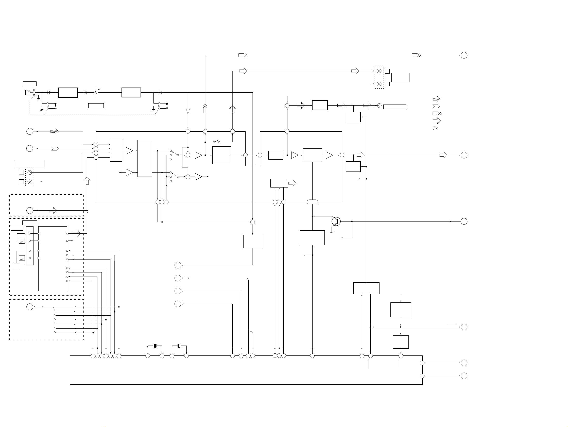
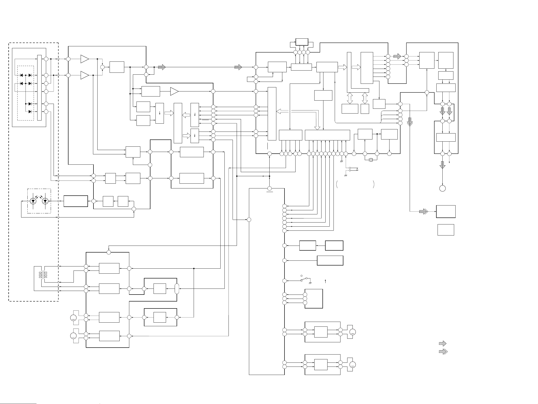
HCD-GRX9000/RX900
7-4. BLOCK DIAGRAM – MAIN Section (1/2) –
J751
MIX MIC
(Page 24)
C
(Page 26)
D
J101 (1/2)
MD/VIDEO (AUDIO) IN
L
R
(HCD-RX900)
(Page 22)
A
ANTENNA
FM 75Ω
AM
(HCD-GRX9000)
B
(Page 22)
(HCD-RX900)
CD-L
PB-L
R-CH
ST-L
FM/AM TUNER UNIT
FM ANT
FM ANT
AM ANT
ST-MUTE
STEREO
AM ANT
TUNED
ST-DIN
ST-DOUT
ST-CLK
ST-CE
MIC AMP
IC750 (1/2)
ST-L
ST-R
ST-MUTE
STEREO
TUNED
ST-DOUT
ST-DIN
ST-CLK
ST-CE
R-CH
RV750
MIC LEVEL
IN B2
68
IN C2
67
IN A2
69
66
SELECT
IN D2
R-CH
GRAPHIC EQUALIZER CONTROL,
ELECTRICAL VOLUME
INPUT
IC101
MIC AMP
IC750 (2/2)
SOUND
CONTROL
CIRCUIT
X501
5MHz
KEY IN2
KEY IN1
60 5
(Page 31)
(Page 31)
(Page 32)
(Page 32)
KEY OUT
75
J
K
L
M
X502
32.768kHz
2
MIC IN
+
+
SPEANA
DATA, CLK
POWER
CD-POWER
REC
REC-L
J101 (2/2)
L
MD/VIDEO
R-CH
R-CH
+
CPU
INTERFACE
DATA
CLOCK
33 32
34
40
VOL OUT2
COMMAND
LATCH
58
A2
EQUALIZER
CONTROL
R-CH
GRAPHIC
CIRCUIT
REC
B2
57
F OUT2
VOL
IN2
42
VOLUME
41
CONTROL
LINE AMP
BASS BOOST
CONTROL
CIRCUIT
BB B2,
BB A2
38, 39
IC191
FEED BACK SWITCH
BUF
OUT2
Q112
MUTING
Q191
36
MUTING
Q113
R-CH
+
SPEANA
MIXING AMP
IC102
CLK
DATA
DBFB CONTROL
R-CH
SWITCH
Q111
R-CH
MUTING CONTROL
SWITCH
Q571, 572
(AUDIO) OUT
R
J191
SUPER WOOFER
+5V
RESET SIGNAL
GENERATOR
IC502
RESET
SWITCH
Q501
• SIGNAL PATH
: CD PLAY
: TAPE PLAY
: RECORD
: TUNER (FM/AM)
: MIC IN
L-CH
FEED-BACK
RESET
E
F
G
N
(Page 26)
(Page 29)
(Page 29)
(Page 31)
52 51
10
68
67
69
ST-DIN
70
TUNED
ST-DOUT
72
STEREO
ST-MUTE
66
65
ST-CE
ST-CLK
05
11
X2
X1
14
13
XT1
XT2
SYSTEM CONTROLLER
IC501 (3/3)
46 5
CD-POWER
POWER
5655
IIC-CLK
IIC-DATA
3
M62442-CLK
M62442-DATA
M62442-LATCH
2
DBFB-H/L
– 27 –
1
16
LINE-MUTE
AC-CUT
15
STK-MUTE
RESET
F-RELAY
– 28 –
100
6
STK-MUTE
RELAY
H
I
(Page 29)
(Page 30)
Page 25
7-5. BLOCK DIAGRAM – MAIN Section (2/2) –
HCD-GRX9000/RX900
F
(Page 28)
G
(Page 28)
R-CH
• SIGNAL PATH
: TUNER (FM/AM)
L-CH
FEED BACK
110
POWER AMP
IC801 (1/2)
17
POWER AMP
IC801 (2/2)
110
POWER AMP
IC821 (1/2)
13
6
D141
RELAY
L-CH (+)
L-CH (–)
OVER LOAD
+
DETECT
Q801, 851
D811
R-CH (+)
-1
-1
D404
D403
D409
-2
D408
(Page 28)
I
J421
PHONES
+
L
–
+
R
–
FAN MOTOR
DRIVE
Q401, 402
TM401
SPEAKER
IMPEDANCE
USE 8 – 16Ω
M401
(FAN)
M
H
(Page 28)
STK-MUTE
05
17
POWER AMP
IC821 (2/2)
6
STANDBY
SWITCH
Q575
13
THP891
TEMPERATURE
DETECT SWITCH
Q891, 892
OVER LOAD
DETECT
Q821, 871
D831
DC DETECT
SWITCH
Q433, 434
OVER LOAD
DETECT SWITCH
Q432, 437
R-CH (–)
RY401
RELAY DRIVE
Q431
RY402
-2
PROTECTOR
Q435, 436
– 29 –
– 30 –
Page 26
HCD-GRX9000/RX900
(
)
7-6. BLOCK DIAGRAM – DISPLAY/KEY CONTROL/POWER SUPPLY Section –
K
(Page 27)
N
(Page 28)
J
(Page 27)
DATA, CLK
RESET
SPEANA
BAND-PASS FILTER
4
LINE IN
REMOTE CONTROL
S601
(JOG DIAL)
= ↔ +
DJ MIX
S602
VOLUME
IC603
F01
17
16
F02
F03
15
14
F04
L+R
13
RST
18
S604 – 625, 631 – 642,
S656 – 659
RECEIVER
IC602
ROTARY
ENCODER
S601
ROTARY
ENCODER
S602
FLUORESCENT INDICATOR TUBE DRIVE,
LED DRIVE, KEY CONTROL
DATA
CLK
24
SDA
SCL
23
10
RESET
34
SPEANA-1
35
SPEANA-2
36
SPEANA-3
37
SPEANA-4
L+R
32
SPEANA RESET
31
26 – 29
KEY-0 – KEY-3
SIRCS
33
JOG-A
21
22
JOG-B
VOL-A
19
VOL-B
20
IC601
SEG1 – SEG24
54 – 69, 72 – 70, 77 – 73
53
GR13
42 – 52
GR2 – GR12
41
GR1
L.SEL
25
LED12 – LED15
79, 3 – 6, 15 – 18
LED1, LED5 – LED8,
11, 12
LED9, LED10
GRID DRIVE
Q621
GRID DRIVE
Q620
D+5V
Q603
LED DRIVE
Q604, 607 – 610,
Q613 – 615, 618
FLUORESCENT
INDICATOR TUBE
FL601
B+ SWITCH
Q601, 602
D610, 612, 620 – 625,
D631 – 633, 651, 652
D613 – 618
CD MECHANISM DECK
SECTION B+
AUDIO D+5V
SYSTEM CONTROLLER
(IC501) B+
FAN MOTOR B–
(FM/AM TUNER CIRCUIT B+)
D+5V
D405 – 407
+10V
B+
SWITCH
Q907, 908
B+
SWITCH
Q905, 906
D507
D501, 502
REGULATOR
CONTROL SWITCH
Q903
TC, PANEL, AUDIO
POWER
CD-POWER
D914
+5V
REGULATOR
IC902
+7V
(CD M+7V)
+7V
–7V
CAPSTAN MOTOR DRIVE CIRCUIT,
TRIGGER PLUNGER DRIVE CIRCUIT B+
+10V
REGULATOR
Q909
+7V
REGULATOR
IC901
+7V
REGULATOR
Q901, 902, 913
–7V
REGULATOR
Q914, 951, 952
+12V
REGULATOR
IC903
(Page 27)
L
(Page 27)
M
RECT
D901 – 904
RECT
D907, 908
POWER TRANSFORMER
T11
X-OUT
X-IN
9
8
X601
05
8MHz
–30V
FL DRIVER (IC601)
FLUORESCENT INDICATOR TUBE
TO
(FL601)
– 31 –
REGULATOR
POWER AMP
(IC801, 821)
–30V
Q910
VF1
VF2
B+
B–
– 32 –
RECT
D909, 910
RECT
D800
(East European, CIS models)
VOLTAGE
SELECT SWITCH
S11
S11
VOLTAGE
SELECTOR
Except East European, CIS models
AC IN
Page 27

7-7. NOTE FOR PRINTED WIRING BOARDS AND SCHEMATIC DIAGRAMS
C
B
These are omitted.
E
Q
(In addition to this, the necessary note is printed in each block.)
Note on Schematic Diagram:
• All capacitors are in µF unless otherwise noted. pF: µµF
50 WV or less are not indicated except for electrolytics
and tantalums.
• All resistors are in W and 1/4 W or less unless otherwise
specified.
• ¢ : internal component.
• 2 : nonflammable resistor.
• 5 : fusible resistor.
• C : panel designation.
Note: The components identified by mark ! or dotted line
with mark ! are critical for safety.
Replace only with part number specified.
• U : B+ Line.
• V : B– Line.
• H : adjustment for repair.
• V oltages are taken with a VOM (Input impedance 10 MΩ).
Voltage variations may be noted due to normal production tolerances.
• Waveforms are taken with a oscilloscope.
Voltage variations may be noted due to normal production tolerances.
• Circled numbers refer to waveforms.
• Signal path.
F : FM
f : AM
E : PB (DECK A)
d : PB (DECK B)
G : REC (DECK B)
J : CD
c : DIGITAL OUT
N : MIC IN
• Abbreviation
EA : Saudi Arabia model.
EE : East European model.
MY : Malaysia model.
SP : Singapore model.
Note on Printed Wiring Boards:
• X : parts extracted from the component side.
• Y : parts extracted from the conductor side.
• ® : Through hole.
• b : Pattern from the side which enables seeing.
(The other layers' patterns are not indicated.)
Caution:
Pattern face side: Parts on the pattern face side seen from
(Side B) the pattern face are indicated.
Parts face side: Parts on the parts face side seen from
(Side A) the parts face are indicated.
• Indication of transistor.
Q
B
CE
These are omitted.
Q
B
CE
These are omitted.
– 33 –
Page 28

7-8. PRINTED WIRING BOARD – TUNER Section (East European, CIS models only) –
• See page 20 for Circuit Boards Location.
• Semiconductor
Location
Ref. No. Location
D21 D-1
D41 D-2
D42 E-3
D43 E-3
D1701 F-2
D1702 F-2
D1703 E-2
D1704 F-2
IC21 D-1
IC41 C-3
IC1701 F-1
IC1702 F-3
Q1 D-1
Q2 D-2
Q3 C-2
Q4 C-2
Q5 C-2
Q9 B-1
Q11 B-3
Q12 A-3
Q13 A-2
Q14 A-2
Q1701 E-2
Q1702 F-2
Q1703 F-2
– 34 –
MAIN BOARD
CN102
(Page 52)
Page 29

7-9. SCHEMATIC DIAGRAM – TUNER Section (East European, CIS models only) –
• See page 75 for Waveforms. • See pages 76 and 77 for IC Block Diagrams.
HCD-GRX9000/RX900
– 35 –
(Page 57)
– 36 –
Note on Schematic Diagram:
• Voltages and waveforms are dc with respect to ground
under no-signal (detuned) conditions.
no mark : FM
( ) : MW
<>: LW
: Impossible to measure
∗
Page 30

HCD-GRX9000/RX900
• Semiconductor
Location
Ref. No. Location
IC101 C-5
IC102 B-5
IC103 C-6
Q101 C-3
7-10. PRINTED WIRING BOARD – CD Section –
• See page 20 for Circuit Boards Location.
( )
MAIN BOARD
CN105
(Page 51)
– 37 –
– 38 –
Page 31

7-11. SCHEMATIC DIAGRAM – CD Section – • See page 75 for Waveforms. • See pages 78 and 79 for IC Block Diagrams.
HCD-GRX9000/RX900
(Page 53)
MAIN BOARD
CN105
( )
( )
( )
Note on Schematic Diagram:
Note: The components identified by mark ! or dotted line
with mark ! are critical for safety.
Replace only with part number specified.
• Voltages and waveforms are dc with respect to ground
under no-signal conditions.
no mark : STOP
( ) : PLAY
: Impossible to measure
∗
– 39 –
– 40 –
Page 32

HCD-GRX9000/RX900
7-12. PRINTED WIRING BOARDS – CD MOTOR Section –
• See page 20 for Circuit Boards Location.
(Page 51)
MAIN BOARD
CN104
(Page 51)
MAIN BOARD
CN103
– 41 –
– 42 –
Page 33

7-13. SCHEMATIC DIAGRAM – CD MOTOR Section –
• See page 80 for IC Block Diagrams.
HCD-GRX9000/RX900
( )
MTZJ-T72
–5.6C
( )
MAIN BOARD
CN104
(Page 53)
MTZJ-T-72-3.6B
MAIN BOARD
CN103
(Page 53)
Note on Schematic Diagram:
• Voltages are dc with respect to ground under no-signal
conditions.
no mark : STOP
– 43 –
– 44 –
Page 34

HCD-GRX9000/RX900
7-14. PRINTED WIRING BOARD – TAPE DECK Section –
• See page 20 for Circuit Boards Location.
()
MAIN BOARD
CN106
(Page 51)
– 45 –
– 46 –
Page 35

7-15. SCHEMATIC DIAGRAM – TAPE DECK Section –
• See page 80 for IC Block Diagram.
()
()
HCD-GRX9000/RX900
MAIN BOARD
(Page 57)
CN106
Note on Schematic Diagram:
Note: The components identified by mark ! or dotted line
with mark ! are critical for safety.
Replace only with part number specified.
– 47 –
• Voltages are dc with respect to ground under no-signal
conditions.
no mark : PLAY
( ) : REC
– 48 –
Page 36

HCD-GRX9000/RX900
7-16. PRINTED WIRING BOARD – LEAF SW Section – • See page 20 for Circuit Boards Location.
( )
MAIN BOARD
7-17. SCHEMATIC DIAGRAM – LEAF SW Section –
( )
CN107
(Page 51)
• Semiconductor Location
Ref. No. Location
D141 G-9
D333 F-2
D334 E-2
D401 G-10
D402 H-9
D403 F-11
D404 F-11
D405 F-10
D406 F-11
D407 F-11
D408 F-11
D409 F-11
D501 E-5
D502 E-5
D503 E-5
D504 E-5
D505 E-6
D506 E-6
D507 E-3
D508 E-2
D901 I-6
D902 I-5
D903 I-6
D904 I-6
D905 G-6
D906 G-7
D907 H-4
D908 H-4
D909 I-5
D910 I-4
D911 I-4
D912 I-4
D913 G-3
D914 G-5
D915 I-3
IC101 D-9
IC102 F-10
IC191 D-11
IC301 B-2
IC381 A-11
IC501 D-4
IC502 E-6
IC901 G-5
IC902 G-3
IC903 H-3
Ref. No. Location
Q111 F-9
Q112 F-9
Q113 H-8
Q161 E-8
Q162 D-8
Q163 H-8
Q191 D-11
Q331 C-2
Q332 D-2
Q333 C-2
Q334 D-2
Q335 C-1
Q336 E-2
Q337 E-2
Q338 F-2
Q339 F-2
Q340 E-2
Q341 E-2
Q342 E-2
Q343 E-2
Q401 E-11
Q402 E-11
Q431 G-9
Q432 H-8
Q433 H-9
Q434 H-8
Q435 H-8
Q436 G-8
Q437 G-8
Q501 E-7
Q571 E-6
Q572 E-6
Q575 F-8
Q901 F-6
Q902 G-6
Q903 G-6
Q905 F-6
Q906 G-6
Q907 G-4
Q908 G-5
Q909 H-4
Q910 I-4
Q913 G-6
Q914 F-7
Q951 G-7
Q952 G-7
( )
( )
( )
( )
( )
( )
( ) ( )
– 49 –
MAIN BOARD
(Page 57)
CN107
Note on Schematic Diagram:
• Voltages are dc with respect to ground under no-signal
conditions.
no mark : PLAY
( ) : REC
: Impossible to measure
∗
– 50 –
Page 37

7-18. PRINTED WIRING BOARD – MAIN Section –
• See page 20 for Circuit Boards Location.
HCD-GRX9000/RX900
(Page 34)
(Page 45)
(Page 49)
(Page 41)
(Page 41)
(Page 38)
(Page 61)
(Page 67)
– 51 –
(Page 70)(Page 73)
– 52 –
Page 38

HCD-GRX9000/RX900
7-19. SCHEMATIC DIAGRAM – MAIN Section (1/4) –
(Page 55)
(Page 40)
(Page 44)
(Page 44)
(Page 57)
(Page 59)
Note on Schematic Diagram:
• Voltages are dc with respect to ground under no-signal
(detuned) conditions.
no mark : FM
( ) : CD
– 53 –
– 54 –
Page 39

7-20. SCHEMATIC DIAGRAM – MAIN Section (2/4) –
HCD-GRX9000/RX900
(Page 72)
(Page 54)
(Page 68)
– 55 –
(Page 59)
Note on Schematic Diagram:
• Voltages are dc with respect to ground under no-signal
(detuned) conditions.
no mark : FM
Note: The components identified by mark ! or dotted line
with mark ! are critical for safety.
Replace only with part number specified.
– 56 –
Page 40

HCD-GRX9000/RX900
7-21. SCHEMATIC DIAGRAM – MAIN Section (3/4) –
(Page 53)
(Page 35)
(Page 48)
(Page 59)
(Page 50)
– 57 –
Note on Schematic Diagram:
• Voltages are dc with respect to ground under no-signal
(detuned) conditions.
no mark: FM [ ] : PB (DECK B)
( ): CD { } : PB (DECK A)
< >: REC
– 58 –
Page 41

7-22. SCHEMATIC DIAGRAM – MAIN Section (4/4) –
• See page 75 for Waveforms.
(Page 54)
HCD-GRX9000/RX900
(Page 55)
(Page 58)
– 59 –
– 60 –
(Page 74)
(Page 64)
Note on Schematic Diagram:
• Voltages are dc with respect to ground under no-signal
(detuned) conditions.
no mark: FM [ ] : PB (DECK B)
( ): CD { } : PB (DECK A)
< >: REC
Page 42

HCD-GRX9000/RX900
7-23. PRINTED WIRING BOARD – PANEL Section –
• See page 20 for Circuit Boards Location.
(Page 51)
(Page 66)
• Semiconductor Location
Ref. No. Location
D602 D-7
D610 D-5
D612 E-4
D613 D-6
D614 F-6
D615 F-6
D616 E-9
D617 E-4
D618 E-7
D620 C-3
D621 C-4
D622 C-5
D623 C-6
D624 C-7
D625 C-8
Ref. No. Location
D651 C-1
D652 D-1
IC601 B-6
IC602 A-9
IC603 B-8
IC750 C-13
Q601 D-6
Q602 D-7
Q603 D-7
Q604 D-5
Q607 B-3
Q608 B-3
Q609 C-6
Ref. No. Location
Q610 C-9
Q618 E-1
Q620 A-7
Q621 A-6
– 61 –
– 62 –
Page 43

7-24. SCHEMATIC DIAGRAM – PANEL Section –
• See page 75 for Waveform. • See page 80 for IC Block Diagrams.
HCD-GRX9000/RX900
(Page 60)
(Page 65)
– 63 –
– 64 –
Note on Schematic Diagram:
• Voltages and waveforms are dc with respect to ground
under no-signal (detuned) conditions.
no mark : FM
Page 44

HCD-GRX9000/RX900
7-25. PRINTED WIRING BOARD – CD-SW Section –
• See page 20 for Circuit Boards Location.
(Page 62)
7-26. SCHEMATIC DIAGRAM – CD-SW Section –
(Page 64)
– 65 –
Note on Schematic Diagram:
• Voltages are dc with respect to groundunder no-signal
(detuned) conditions.
no mark : FM
– 66 –
Page 45

HCD-GRX9000/RX900
7-27. PRINTED WIRING BOARD – HP Section –
• See page 20 for Circuit Boards Location.
7-28. SCHEMATIC DIAGRAM – HP Section –
(Page 56)
(Page 51)
– 67 – – 68 –
Page 46

HCD-GRX9000/RX900
7-29. PRINTED WIRING BOARDS – POWER AMP Section –
• See page 20 for Circuit Boards Location.
(Page 73)
• Semiconductor
Location
AMP (R) BOARD
Ref. No. Location
D821 B-3
D831 C-3
D871 B-2
D891 C-3
D892 B-3
IC821 A-3
Q821 B-3
Q871 B-2
Q891 A-4
Q892 A-4
(Page 70)
(Page 70)
• Semiconductor
Location
AMP (L) BOARD
Ref. No. Location
D800 C-4
D801 B-2
D811 D-2
D841 C-3
D842 B-3
D851 E-2
(Page 69)
(Page 69)
(Page 51)
IC801 C-1
Q801 B-2
Q851 E-2
– 69 – – 70 –
Page 47

7-30. SCHEMATIC DIAGRAM – POWER AMP Section –
HCD-GRX9000/RX900
Note on Schematic Diagram:
• Voltages are dc with respect to ground under no-signal
(detuned) conditions.
no mark : FM
(Page 74)
(Page 55)
Note: The components identified by mark ! or dotted line
with mark ! are critical for safety.
Replace only with part number specified.
– 71 – – 72 –
Page 48

HCD-GRX9000/RX900
7-31. PRINTED WIRING BOARD – TRANSFORMER Section –
• See page 20 for Circuit Boards Location.
7-32. SCHEMATIC DIAGRAM – TRANSFORMER Section –
(Page 72)
(Page 60)
Note: The components identified by mark ! or dotted line
with mark ! are critical for safety.
Replace only with part number specified.
(Page 51) (Page 70)
– 73 –
– 74 –
Page 49

• Wavef orms
3.6 Vp-p
126 ns
– TCB Board –
(East European, CIS)
1 IC21 @¢ (XOUT)
4.5 MHz
– BD Board –
1 IC101 #£ (RF O) (PLAY MODE)
4.2 Vp-p
+0.25
1.3 Vp-p
–0.20
4 IC103 @¶ (MDP)
5 IC103 ^º (XPCK)
230 µs
8 IC103 *ª (XTAI)
2.5 Vp-p
2.6 Vp-p
16.9344 MHz
7.8 µs
– MAIN Board –
1 IC501 !¡ (X1)
5 Vp-p
4.4 Vp-p
200 ns
2 IC101 2 (FEI) (PLAY MODE)
3 IC101 $¶ (TEI) (PLAY MODE)
Approx.
0.5 Vp-p
Approx.
0.2 Vp-p
6 IC103 ^™ (RFCK)
135 µs
7 IC103 &¢ (WFCK)
5 Vp-p
5 Vp-p
2 IC501 !¢ (XT1)
2.2 Vp-p
30.6 µs
– PANEL Board –
3 IC601 9 (X-IN)
135 µs
– 75 –
Page 50

• IC Block Diagrams
– TCB Board –
IC21 LC72130 (East European, CIS models)
XOUT
VSS
AOUT2
AIN2
21222324
PD2
20
PHASE DETECTOR
CHARGE PUMP
19 18 17 16 15 14
PD1
AIN1
AOUT1
VDD
FMIN
AMIN
IO2
13
UNLOCK
DETECTOR
REFERENCE
DIVIDER
2
B
C
I/F
2 345 6 7 8 9 10
1
CL
CE
D0
BO5
D1
XIN
SWALLOW COUNTER
1/16, 1/17 4BITS
12BITS PROGRAMMABLE
DRIVER
DATA SHIFT REGISTER LATCH
BO1
BO2
POWER
BO3
IC41 LA1838 (East European, CIS models)
ON
RESET
BO4
1/2
UNIVERSAL
COUNTER
1211
IO1
IFIN
OSC.BUFF
FM-SD.ADJ
ALC
BUFF
COMP
FM
S METER
FM
IF
1
FM-IN
SD
AM-OSC
REG
28
REG
AM
AM
OSC
MIX
AM/FM
S-CURVE
FM
DET
BUFF
2 3 4 5 6 7 98
AM-MIX
AM
RF. AMP
IF
FM-IF
FM-AFC
AM-RF-IN
AGC
AM
IF
S METER
TUNING
DRIVE
AM-IF
AM
GND
AGC
GND
DET
FM-DET OUT
AM-DET OUT
TUNED
VCC
STEREO
VCC
MPX-IN
FM DET
AM. SD
OUT L
OUT R
20 19 18 17 16
212223242527 262930
DECODER
ANTI BIRDIE
STEREO
12
AM. SD ADJ
PILOT
DET
13
SW
IF-BUFF
MUTE
FF
VCO
FM. SD
STEREO
DRIVE
FF FF
PHASE
DET
AMP-IN L
AM/FM
AMP-IN R
AMP OUT L
MUTE
AMP OUT R
15141110
VCO-STOP
– 76 –
Page 51

IC1701 IR3R42 (East European, CIS models) IC1702 µPD4053BC (East European, CIS models)
SUBIN
SUBOUT
AMP
1
VCC
MON
1/2
PHASE
AMP
2 3
IN
WAVEFORM
SEP.
GATE
POUT
20 19 18 17 16 15 14 13 12
REGULATOR
VCO
OSC
1/2
SAMPLE
& HOLD
BUFFER
4
RHC
LPF1A
LPF1B
DETIN
AMP
PHASE
COMPARATOR
COMPARATOR 2
5 6 7 8 9
ROUT
LOUT
ST
LHC
LPF2A
PHASE
MUTE
VCO STOP
LPF2B
11
TRIGGER
10
GND
LAMP
C.COM
INH
VEE
VSS
1
B1
B0
2
C1
3
4
5
CO
6
7
8
OPEN
OPEN
OPEN
VDD
16
B.COM
15
14
A.COM
13
A1
A0
12
11
A
10
B
C
9
– 77 –
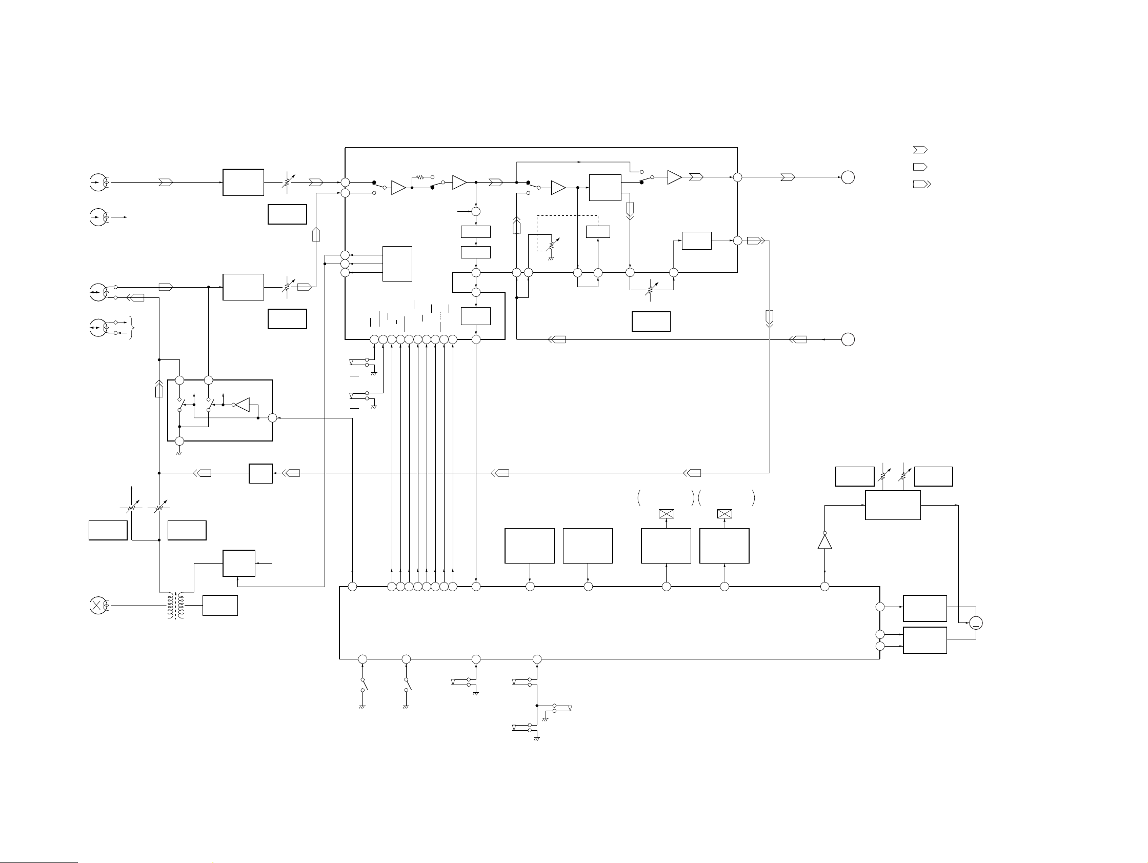
Page 52

– BD Board –
IC101 CXA1992AR
+
PD2 IV
AMP
FE_BIAS
40
VEE
BAL1
TOG2
TOG1
–
+
–
+
VCC
FZC COMP.
–
+
F IV AMP
–
+
E IV AMP
BAL2
BAL3
TOG4
TOG3
+
–
ATSC
WINDOW
COMP.
–
+
TZC COMP.
+
–
BAL4
VCC
+
–
VEE
TEO
LPFI
ATSC
TDFCT
F
41
E
42
43
EI
44
VEE
45
46
47
TEI
48
49
TZC
50
51
VC
FZC
52
PD2
–
+
–
+
–
1
FEO
PD1
–
+
PD1 IV
AMP
TGFL
–
+
E-F BALANCE
WINDOW COMP.
DFCT
2 3
FEI
VCC
TM1
VCC
IFB1
VEE
+
–
IFB2
PD
+
APC
DFCT
FDFCT
VEE
–
IFB3
LD
+
–
+
–
VEE
LASER POWER CONTROL
FE AMP
IFB4
IFB5
IFB6
+
–
TRK. GAIN
WINDOW COMP.
+
–
TG1
FOCUS
PHASE COMPENSATION
FS4
4
FGD
CP
RF_I
–
+
VEE
MIRR
VCC
–
+
–
–
+
+
–
+
VEE
LEVEL S
VCC
–
+
–
+
RF SUMMING
AMP
RF_O
+
–
+
–
–
–
FO. BIAS
WINDOW
COMP.
RF_M
+
–
+
–
RFTC
+
+
–
FOK
LDON
LPCL
LPC
FOH
FOL
TGH
TGL
BALH
BALL
ATSC
TZC
FZC
TRACKING
PHASE COMPENSATION
TGFL
DFCTO
IIL DATA REGISTER
INPUT SHIFT REGISTER
ADDRESS DECODER
SENS SELECTOR
OUTPUT DECODER
IFB1-6
FS1-4 TG1-2 TM1-7 PS1-4
BAL1-4
TOG1-4
VCC
FS1
+
FS2
–
Charge
up
VEE
5 6 7 8 9 10
FLB
FE_O
FE_M
SRCH
TGU
FOK
CC1
CB
CC2
27282930313233343536373839
–
+
SENS2
26
+
–
IIL
↓
VCC
–
+
–
VEE
+
–
+
TTL
DFCT
+
MIRR
IIL
↓
TTL
DFCT1
CC1
TTL
↓
IIL
VCC
ISET
VCC VCC
SENS1
25
C. OUT
24
XRST
23
DATA
22
XLT
21
CLK
20
LOCK
19
VCC
18
ISET
17
SL_O
16
TM4 TM6
SL_M
15
TM7
TM3
FSET
TG2
TM5
–
SL_P
14
+
VEEVEE
TM2
–
+
131211
TG2
FSET
TA_M
TA_O
– 78 –
Page 53

IC102 BA5941FP-E2
IN4B
IN4A
IN3B
27
28
26
IN3A
OP OUT
OP IN (–)
OP IN (+)
24
25
22
23
GND
21 20
NC
VCC
OUT3A
18
19
OUT3B
1617
OUT4A
OUT4B
15
NC
+
–
Vcc
–
+
–
+
–
+
–
+
1 2
VCC
BIAS IN
IC103 CXD2519Q
–
+
–
+
+
–
+
–
MUTE
4
3
IN1B
IN1A
6
IN2A
7
GND
5
IN2B
8
GND
9
MUTE
VccVcc
10
VCC
LEVEL SHIFT
LEVEL SHIFT
+
–
11
OUT2A
+
–
12 13
OUT2B
LEVEL SHIFT
LEVEL SHIFT
+
–
OUT1A
+
–
14
OUT1B
AVSS
AVDD
AOUT1
AIN1
LOUT1
AVSS
XVDD
XTAI
XTAO
XVSS
AVSS
LOUT2
AIN2
AOUT2
AVDD
AVSS
XRST
SYSM
VDD
VSS
EXCK
SBSO
SCOR
WFCK
EMPHI
EMPH
DOUT
C4M
FSTT
XTSL
MNT0
MNT1
MNT3
XROF
C2PO
RFCK
GFS
XPCK
XUGF
GTOP
VDD
VSS
BCKI
BCK
PCMDI
PCMD
69 68
80
79 78
81
NC
82
83
84
85
86
87
88
89
90
91
92
93
94
95
96
97
98
NC
99
NC
100
–
+
–
+
SERIAL-IN
INTERFACE
1 234
VDD
VSS
LMUT
77
OVER SAMPLING
TIMING
LOGIC
76 75 74
–
+
–
+
DIGITAL FILTER
RMUT
73 72
PWMPWM
INTERFACE
56789 10
TES2
SQCK
CKOUT
70
71
3RD-ORDER NOISE SHAPER
CPU
12 13
11
XLAT
SENS
DATA
SQSO
67
EFM
DEMODURATOR
SUB CODE
PROCESSOR
14
SEIN
CLOK
66 65 64
15 16 17
CNIN
DATO
63 62
SERVO
AUTO
SEQUENCER
18 19
XLTO
CLKO
SPOA
60
61
ERROR
CORRECTOR
16K RAM
21
20
SPOB
SPOC
SPOD
59 58
22 23
XLON
57
24
FOK
56 55 54
D / A
INTERFACE
DIGITAL OUT
25 26 27
VSS
VDD
DIGITAL CLV
MDP
MON
53 52 51
28 29 30
MDS
LOCK
LRCKI
PWMI
ASYMMETRY
CORRECTOR
DIGITAL
PLL
OSC
CLOCK
GENERATOR
LRCK
50
WDCK
49
48
ASYE
47
ASYO
46
ASYI
BIAS
45
44
RF
AVDD
43
42
CLTV
AVSS
41
40
FILI
FILO
39
38
PCO
37
VCTL
36
V16M
35
VCKI
VPCO1
34
33
VPCO2
32
TES1
31
TES0
– 79 –
Page 54

– MOTOR (TURN) Board –
– PANEL Board –
IC701 M54641L
VCC VCC
1
REG
IN1
IN2
INPUT
3
AMP.
CONTROL
INPUT
6
AMP.
4
GND
– MOTOR (SLIDE) Board –
IC801 BA6286N
POWER
AMP.
POWER
AMP.
IC603 BA3833F-E2
8
RESET
REFERENCE
5
OUT2
2
OUT1
7
C
PREF
LINE
NF
LINE
IN
GND
BIAS
1
REFFERENCE
2
CURRENT
3
4
5
6
Bias
C
7
NC
8
NC
9
NC
RESET
BPF
BPF DET
BPF DET
BPF DET
DET
DET
18
RESET
17
f01
16
f02
15
f03
14
f04
13
f
12
VCC
11
NC
10
NC
GND
1
RIN
2
VREF
3
OUT2
4
RNF
5
GND
6
7
OUT1
VM
8
VCC
9
FIN
10
– AUDIO Board –
IC602 µPC1330HA
TSD
POWER
SAVE
CONTROL
LOGIC
INVERTER
2
1
SW R1 GND SW P1
3
4
CONT
COMPARATER
5
VCC
GND
6
SW P2 GND
7 8 9
SW R2
– 80 –
Page 55

7-33. IC PIN FUNCTION DESCRIPTION
• MAIN BOARD IC501 µPD780018AYGF-012-3BA (SYSTEM CONTROLLER)
Pin No. Pin Name I/O Function
1 LINE-MUTE O
2 DBFB-H/L O
M62442-LATCH
3
KEYCON-LATCH
4
5 POWER O
6 F-RELAY O
7 R-RELAY O
8 PL-RELAY O
9 VPP —
10 X2 O
11 X1 I
12 VDD —
13 XT2 O
14 XT1 I
15 RESET I
16 AC-CUT I
17 CAPM-CNT1P O
18 SCOR I
19 SOFT-TEST O
20 NCO O
21 RDS-INT I
22 RDS-DATA I
23 AVDD —
24 AVREF I
25 ADJ I
26 A-SHUT I
27 B-SHUT I
28 B-HALF I
29 CLK-CHECK I
30 SPEC-IN I
31 AMS-IN I
DEMO-CHANGE
32
33 AVSS —
34 SQ-DATA-IN I
35 NCO O
36
SQ-CLK
(D-OUT ON/OFF)
Line muting on/off control signal output terminal “L”: muting on
DBFB normal/high selection signal output to the M62442FP (IC101)
“L”: DBFB high, “H”: DBFB low
O
Serial data latch pulse output to the M62442FP (IC101)
O
Serial data latch pulse output terminal Not used (open)
Power on/off control signal output for the audio system (+5V) and deck, panel, audio system
(+7V) “L”: power on, “H”: standby
Relay drive signal output for the speaker protect “H”: on
Relay drive signal output for the speaker protect “H”: on Not used (open)
Relay drive signal output for the speaker protect “H”: on Not used (open)
Ground terminal
Main system clock output terminal (5 MHz)
Main system clock input terminal (5 MHz)
Power supply terminal (+5V)
Sub system clock output terminal (32.768 kHz)
Sub system clock input terminal (32.768 kHz)
System reset signal input from the reset signal generator (IC502) “L”: reset
For several hundreds msec. after the power supply rises, “L” is input, then it changes to “H”
AC off detection signal input from the reset signal generator (IC502)
Capstan motor (M1) drive signal output terminal
Subcode sync (S0+S1) detection signal input from the CXD2519Q (IC103)
Output terminal for the software test (open)
Not used (open)
Serial data reading clock signal input terminal Not used (fixed at “L”)
Serial data input terminal Not used (fixed at “L”)
Power supply terminal (+5V) (for A/D conversion)
Reference voltage (+5V) input terminal (for A/D conversion)
Setting terminal for the CD test mode Normally: fixed at “H”
Shut off detection signal input from the deck-A side reel pulse detector (IC1001)
Shut off detection signal input from the deck-B side reel pulse detector (IC1002)
Detection input from the deck-B half detect switch (S1006)
Not used (fixed at “L”)
Setting terminal for the version
Automatic music sensor detection signal input from the HA12215F (IC301)
I
Setting terminal for the demonstration H/L Fixed at “L”
Ground terminal (for A/D conversion)
Sub-code Q data input from the CXD2519Q (IC103)
Not used (open)
O
Sub-code Q data reading clock signal output to the CXD2519Q (IC103)
SUPERWOOFER-
37
38
ON/OFF
SUPERWOOFER
MODE
39 NIL I
40 VSS —
41 DELAY-CONT O
42 PL-LATCH O
O
Super woofer speaker on/off control signal output terminal Not used (open)
O
Super woofer speaker mode control signal output terminal Not used (open)
Not used (fixed at “L”)
Ground terminal
Serial data latch pulse output terminal Not used (open)
Serial data latch pulse output terminal Not used (open)
– 81 –
Page 56

Pin No. Pin Name I/O Function
43 COM-DIN I
44 COM-DOUT O
45 COM-CLK O
46 CD-POWER O
47 CD-DATA O
48 CD-CLK O
49 PL-CLK O
50 PL-DATA O
51 M62442-CLK O
52 M62442-DATA O
53
54
55 IIC-DATA I/O
56 IIC-CLK I/O
57 XRST O
58 XLT O
59 FOCUS-SW O
60 TBL-L O
61 TBL-R O
62 NCO O
63 LOAD-OUT O
64 LOAD-IN O
65 ST-CLK O
66 ST-DIN I
67 ST-DOUT O
68 ST-CE O
69 TUNED I
70 STEREO I
71 VSS —
72 ST-MUTE O
73 SENS2 I
74 SENS I
LEVEL-CONT-A
LEVEL-CONT-B
Serial data input terminal Not used (fixed at “L”)
Serial data output terminal Not used (open)
Serial data transfer clock signal output terminal Not used (open)
Power on/off control signal output for the CD mechanism deck section
“H”: power on, “L”: standby
Serial data output to the CXD2519Q (IC103)
Serial data transfer clock signal output to the CXD2519Q (IC103)
Serial data transfer clock signal output terminal Not used (open)
Serial data output terminal Not used (open)
Serial data transfer clock signal output to the M62442FP (IC101)
Serial data output to the M62442FP (IC101)
O
Level control signal output terminal Not used (open)
O
Level control signal output terminal Not used (open)
Communication data bus with the fluorescent indicator tube driver (IC601)
Communication data reading clock signal input or transfer clock signal output with the fluo-
rescent indicator tube driver (IC601)
Reset signal output to the CXA1992AR (IC101), BA5941FP (IC102) and CXD2519Q (IC103) on
the CD mechanism deck section “L”: reset
Serial data latch pulse output to the CXD2519Q (IC103)
Focus control signal output terminal Not used (open)
Motor drive signal output to the disc tray turn motor driver (IC701) *1
Motor drive signal output to the disc tray turn motor driver (IC701) *1
Not used (open)
Motor drive signal output to the disc tray slide motor driver (IC801) *2
Motor drive signal output to the disc tray slide motor driver (IC801) *2
PLL serial data transfer clock signal output to the FM/AM tuner unit or PLL (IC21)
PLL serial data input from the FM/AM tuner unit or PLL (IC21)
PLL serial data output to the FM/AM tuner unit or PLL (IC21)
PLL chip enable signal output to the FM/AM tuner unit or PLL (IC21)
Tuning detection signal input from the FM/AM tuner unit or LA1838 (IC41) “L”: tuned
FM stereo detection signal input from the FM/AM tuner unit or LA1838 (IC41) “L”: stereo
Ground terminal
Tuner muting control signal output to the FM/AM tuner unit or LA1838 (IC41) “L”: muting on
Internal status (SENSE) signal input from the CXA1992AR (IC101)
Internal status (SENSE) signal input from the CXD2519Q (IC103)
*1 Disc tray turn motor (M701) control
Mode
Terminal
TBL-L (pin ^º)
TBL-R (pin ^¡)
STOP
“H” “L” “H” “L”
“H” “H” “L” “L”
*2 Disc tray slide motor (M801) control
Mode
Terminal
LOAD-OUT (pin ^£)
LOAD-IN (pin ^¢)
STOP TABLE IN TABLE OUT BRAKE
“H” “H” “L” “L”
“H” “L” “H” “L”
COUNTER-
CLOCKWISE
– 82 –
CLOCKWISE BRAKE
Page 57

Pin No. Pin Name I/O Function
75 DISC-SENS I
76 TBL-SENS I
77 CAPM-CNT2P O
78 ENC3 I
79 ENC2 I
80 ENC1 I
81 OUT-OPEN I
82 CAP-M-H/L O
83 B-TRG O
84 A-TRG O
85 CAPM-CNT1M O
86 CAPM-CNT2M O
87 TC-MUTE O
88 R/P-PASS O
89 NR-ON/OFF O
90 REC-MUTE O
91 CLK-OUT O
92 BIAS O
93 EQ-H/N O
94 PB-A/B O
95 A-PLAY-SW I
96 B-PLAY-SW I
97 TC-RELAY O
98 A-HALF I
99 ALC-ON/OFF O
100 STK-MUTE O
Disc status detection signal input from the disc sensor (IC703)
Disc tray status detection signal input from the disc tray sensor (IC702)
Capstan motor drive signal output terminal Not used (open)
Detection signal input from the disc tray address detect rotary encoder (S811)
Detection signal input from the disc tray open/close detect switch (S801)
“L”: open, “H”: close
High/normal speed selection signal output of the capstan motor (M1)
“L”: high speed, “H”: normal speed
Deck-B side trigger plunger (SL2) drive signal output terminal
Deck-A side trigger plunger (SL1) drive signal output terminal
Capstan motor (M1) drive signal output terminal
Capstan motor (M1) drive signal output terminal
Line muting on/off selection signal output to the HA12215F (IC301)
“L”: muting off, “H”: muting on
Recording/playback/pass selection signal output to the HA12215F (IC301)
“L”: recording mode
Dolby NR on/off selection signal output to the HA12215F (IC301)
“L”: dolby off, “H”: dolby on
Recording muting on/off selection signal output to the HA12215F (IC301)
“L”: muting on, “H”: muting off
Clock output for the check Not used (open)
Recording bias on/off selection signal output to the HA12215F (IC301)
“L”: bias off, “H”: bias on
Normal/high speed selection signal output to the HA12215F (IC301)
“L”: normal speed, “H”: high speed
Deck-A/B selection signal output to the HA12215F (IC301) “L”: deck-A, “H”: deck-B
Detection input from the deck- A play detect switch (S1001) “H”: deck-A play
Detection input from the deck- B play detect switch (S1002) “H”: deck-B play
Recording/playback select signal output to the REC/PB switch (IC602)
“L”: playback, “H”: recording
Detection input from the deck-A cassette detect switch (S1003)
“L”: cassette in, “H”: no cassette
Automatic limiter control signal output to the HA12215F (IC301) “L”: limiter on
Power amplifier on/off selection signal output terminal “L”: on, “H”: standby
– 83 –
Page 58

• PANEL BOARD IC601 TMP87CM74AF-6671
(FLUORESCENT INDICATOR TUBE DRIVE, LED DRIVE, KEY CONTROL)
Pin No. Pin Name I/O Function
1 LED3 O
2 LED4 O
3 LED5 O
4 LED6 O
5 LED7 O
6 LED8 O
7 VSS —
8 X-OUT O
9 X-IN I
10 RESET I
11 LED9 O
12 LED10 O
13 TEST I
14 LED11 O
15 LED12 O
16 LED13 O
17 LED14 O
18 LED15 O
19 VOL-A I
20 VOL-B I
21 JOG-A I
22 JOG-B I
23 SCL I/O
24 SDA I/O
25 L.SEL O
26 KEY-0 I
27 KEY-1 I
28 KEY-2 I
LED drive signal output terminal Not used (open)
LED drive signal output terminal Not used (open)
LED drive signal output terminal (DISC 3)
LED drive signal output terminal (DISC 2)
LED drive signal output terminal (DISC 1)
LED drive signal output terminal (ENTER/NEXT, GROOVE)
Ground terminal
System clock output terminal (8 MHz)
System clock input terminal (8 MHz)
System reset signal input from the reset signal generator (IC502) “L”: reset
For several hundreds msec. after the power supply rises, “L” is input, then it changes to “H”
LED drive signal output terminal (JOG, DJ MIX)
LED drive signal output terminal (NON-STOP, + ), – 0)
Connected to ground
LED drive signal output terminal Not used (open)
LED drive signal output terminal (EFFECT)
LED drive signal output terminal (CD ( P)
LED drive signal output terminal (TAPE B (/9)
LED drive signal output terminal (TAPE A (/9)
Rotary encoder pulse input from the S602 (VOLUME)
Rotary encoder pulse input from the S602 (VOLUME)
Jog dial pulse input from the S601 (= ↔ + DJ MIX)
Jog dial pulse input from the S601 (= ↔ + DJ MIX)
Communication data reading clock signal input or transfer clock signal output with the system
controller (IC501)
Communication data bus with the system controller (IC501)
LED selection signal output terminal
Key input terminal (A/D input) (S604 to 617)
EFFECT, SURROUND, KARAOKE PON/MPX, p, TIMER SELECT, CLOCK/TIMER SET,
DISPLAY/DEMO, FILE SELECT, GEQ CONTROL, P FILE MEMORY, FUNCTION,
REPEAT STEREO/MONO, EDIT DIRECTION, PLAY MODE DOLBY NR TUNER
MEMORY keys input
Key input terminal (A/D input) (S619 to 625)
FLASH, NON-STOP, – 0, ENTER/NEXT, + ) , DBFB, GROOVE keys input
Key input terminal (A/D input) (S631 to 642)
TUNER BAND, CD ( P, TAPE B (/9, TAPE A (/9, ON/STANDBY, DISC 1/2/3,
DISC SKIP/EX-CHANGE, 6 keys input
29 KEY-3 I
30 MODEL I
31
32 L+R I
33 SIRCS I
34 SPEANA-1 I
SPEANA
RESET
Key input terminal (A/D input) (S618, 656 to 659)
r REC, P PAUSE, HI-DUB, CD SYNC, keys input
Destination setting terminal
O
Reset signal output the spectrum analyzer band-pass filter (IC603) “H”: reset
Spectrum analyzer drive signal input from the spectrum analyzer band-pass filter (IC603)
(for VACS, non-stop signal)
Remote control signal input from the remote control receiver (IC602)
Spectrum analyzer drive signal input from the spectrum analyzer band-pass filter (IC603)
(for low frequency)
– 84 –
Page 59

Pin No. Pin Name I/O Function
35 SPEANA-2 I
36 SPEANA-3 I
37 SPEANA-4 I
38 VASS —
39 VAREF I
40 VDD —
41 to 53 GR1 to GR13 O
54 to 69
70 to 72
73 to 77
SEG1 to SEG16
SEG19 to SEG17
SEG24 to SEG20
78 VKK —
79 LED1 O
80 LED2 O
Spectrum analyzer drive signal input from the spectrum analyzer band-pass filter (IC603)
(for low and middle frequency)
Spectrum analyzer drive signal input from the spectrum analyzer band-pass filter (IC603)
(for middle and high frequency)
Spectrum analyzer drive signal input from the spectrum analyzer band-pass filter (IC603)
(for high frequency)
Ground terminal (for A/D conversion)
Reference voltage (+5V) input terminal (for A/D conversion)
Power supply terminal (+5V)
Grid drive signal output to the fluorescent indicator tube (FL601)
O
Segment drive signal output to the fluorescent indicator tube (FL601)
O
Segment drive signal output to the fluorescent indicator tube (FL601)
O
Segment drive signal output to the fluorescent indicator tube (FL601)
Power supply terminal (–30V) (for fluorescent indicator tube drive)
LED drive signal output terminal (r REC, P PAUSE)
LED drive signal output terminal Not used (open)
– 85 –
Page 60

SECTION 8
EXPLODED VIEWS
NOTE:
• -XX and -X mean standardized parts, so they
may have some difference from the original
one.
• Color Indication of Appearance Parts
Example:
KNOB, BALANCE (WHITE) . . . (RED)
• Abbreviation
• Abbreviation
EA : Saudi Arabia
EA : Saudi Arabia
EE : East European
EE : East European
IA : Indonesia
IA : Indonesia
MY : Malaysia
MY : Malaysia
SP : Singapore
SP : Singapore
↑↑
Parts Color Cabinet's Color
(1) CASE SECTION
5
• Items marked “*” are not stocked since they
are seldom required for routine service. Some
delay should be anticipated when ordering
these items.
• The mechanical parts with no reference number in the exploded views are not supplied.
• Hardware (# mark) list and accessories and
packing materials are given in the last of the
electrical parts list.
9
8
7
The components identified by
mark ! or dotted line with mark
! are critical for safety.
Replace only with part number
specified.
#1
#3
Front panel section
4
2
#5
8
6
7
#3
3
1
#2
#2
TCM-230AWR1
TCM-230PWR1
Ref. No. Part No. Description Remark
1 1-773-025-11 WIRE (FLAT TYPE) (15 CORE) (33cm)
2 X-4949-350-1 LID (R) ASSY, CASSETTE
3 1-773-048-11 WIRE (FLAT TYPE) (17 CORE)
4 X-4949-349-1 LID (L) ASSY, CASSETTE
5 4-996-703-51 PANEL, LOADING (EE, CIS)
5 4-996-703-61 PANEL, LOADING (E, EA, MY, SP)
Ref. No. Part No. Description Remark
6 1-769-984-11 WIRE (FLAT TYPE) (13 CORE) (23cm)
7 3-363-099-11 SCREW (CASE 3 TP2) (3X8)
8 3-363-099-71 SCREW (CASE 3 TP2) (3X12)
* 9 4-996-728-01 CASE (EXCEPT IA)
* 9 4-996-728-21 CASE (IA)
– 86 –
Page 61

(2) FRONT PANEL SECTION
not supplied
58
54
57
58
53
59
supplied with
J751
60
#2
58
58
58
r
A
58
58
r
B
61
(including rA, rB)
62
supplied with J421
58
58
#7
64
not supplied
65
57
63
58
56
52
55
#7
54
63
51
not supplied
Ref. No. Part No. Description Remark Ref. No. Part No. Description Remark
51 X-4949-385-1 PANEL ASSY, FRONT
52 4-930-336-61 FOOT (FELT)
53 4-962-708-11 EMBLEM (4-A), SONY
54 4-995-081-01 LATCH, DC
55 4-996-722-01 KNOB (VOL)
56 4-996-721-01 KNOB (JOG-U4)
* 57 4-996-716-01 HOLDER (CDM)
58 4-951-620-01 SCREW (2.6X8), +BVTP
59 4-986-893-51 KNOB (MICROPHONE)
* 60 1-668-206-11 CD-SW BOARD
* 61 A-4407-170-A PANEL BOARD, COMPLETE (EE, CIS)
* 61 A-4407-171-A PANEL BOARD, COMPLETE (EA)
* 61 A-4407-172-A PANEL BOARD, COMPLETE (E, MY, SP)
* 62 1-668-209-11 HP BOARD
* 63 3-973-975-21 DAMPER, OIL
64 4-996-732-01 SPRING (A DECK)
65 4-996-733-01 SPRING (B DECK)
– 87 –
Page 62

(3) CHASSIS SECTION
CDM38LH-5BD29AL
106
#2
104
#6
T11
not supplied
#2
#4
#2
not supplied
103
108
105
M401
#2
107
B
#2
#2
#1
#2
A
#2
115
113
E
114
EA, MY, SP
113
EE, CIS, EA,
MY, SP
#4
not supplied
102
101
A
EE, CIS
109
110
B
#2
111
112
– 88 –
Page 63

Ref. No. Part No. Description Remark
* 101 3-703-244-00 BUSHING (2104), CORD (EE, CIS, EA, MY, SP)
101 3-703-571-11 BUSHING (S) (4516), CORD (E)
* 102 A-4407-181-A AMP (L) BOARD, COMPLETE (EE, CIS)
* 102 A-4407-182-A AMP (L) BOARD, COMPLETE (E, EA, MY, SP)
* 103 A-4407-185-A AMP (R) BOARD, COMPLETE (EE, CIS)
* 103 A-4407-186-A AMP (R) BOARD, COMPLETE (E, EA, MY, SP)
* 104 1-668-212-11 TRANSFORMER BOARD
105 1-783-570-11 WIRE (FLAT TYPE) (19 CORE)
* 106 4-996-846-01 PANEL, BACK (E)
* 106 4-996-846-11 PAENL, BACK (MY, SP)
* 106 4-996-846-21 PANEL, BACK (EA)
* 106 4-996-846-51 PANEL, BACK (EE, CIS)
107 1-693-420-11 TUNER (FM/AM) (E)
107 1-693-421-11 TUNER (FM/AM) (EA, MY, SP)
107 A-4303-587-A TCB BOARD, COMPLETE (EE, CIS)
108 1-769-976-11 WIRE (FLAT TYPE) (13 CORE) (14cm) (E)
Ref. No. Part No. Description Remark
108 1-773-008-11 WIRE (FLAT TYPE) (15 CORE) (14cm)
(EXCEPT E)
109 4-924-098-91 HOLDER, PC BOARD (EE, CIS)
* 110 A-4407-152-A MAIN BOARD, COMPLETE (EE, CIS)
* 110 A-4407-153-A MAIN BOARD, COMPLETE (EA, MY, SP)
* 110 A-4407-154-A MAIN BOARD, COMPLETE (E)
111 4-965-822-01 FOOT
* 112 4-988-533-01 HOLDER, PWB
! 113 1-575-651-11 CORD, POWER (EE, CIS, EA, MY, SP)
! 113 1-575-653-11 CORD, POWER (E)
! 114 1-569-008-21 ADAPTOR, CONVERSION 2P (EA, MY, SP)
115 4-999-706-01 COVER (BPAT)
M401 1-763-072-11 FAN, D.C.
! T11 1-431-662-11 TRANSFORMER, POWER (EE, CIS)
! T11 1-431-663-11 TRANSFORMER, POWER (EXCEPT EE, CIS)
The components identified by mark ! or dotted
line with mark ! are critical for safety.
Replace only with part number specified.
– 89 –
Page 64

(4) CD MECHANISM DECK SECTION-1
(CDM38LH-5BD29AL)
202
201
211
203
201
205
#8
209
204
M701
212
206
#2
207
208
210
#2
Ref. No. Part No. Description Remark
201 4-981-789-11 BRACKET (2), YOKE
202 4-977-945-01 TRAY (TURN)
203 X-4946-665-1 SHAFT ASSY, WORM
204 4-977-943-01 BELT (TURN) (1.2)
205 4-977-956-01 WHEEL, WORM
* 206 1-658-577-11 MOTOR (TURN) BOARD
207 4-988-162-01 ROLLER
Ref. No. Part No. Description Remark
208 4-977-941-01 BEARING (WORM)
* 209 1-658-576-11 SENSOR BOARD
210 4-934-376-01 SHAFT (ROLLER)
211 4-981-187-01 COLLAR (WORM)
212 4-977-944-01 TRAY (SLIDE)
M701 A-4672-004-A MOTOR ASSY (TURN)
– 90 –
Page 65

(5) CD MECHANISM DECK SECTION-2
(CDM38LH-5BD29AL)
251
267
268
266
261
259
258
254
269
#2
251
261
256
253
252
255
257
not
supplied
270
260
M801
BU-5BD29AL
S811
263
263
265
251
Ref. No. Part No. Description Remark
251 4-981-789-11 BRACKET (2), YOKE
252 4-977-954-01 PULLEY (SL)
253 4-977-953-01 GEAR (SL-A)
254 4-977-955-01 GEAR (SL-B)
255 4-977-942-01 BELT (SL) (1.4)
256 X-4946-667-1 CAM ASSY, BU
257 1-452-925-21 MAGNET ASSY
258 1-776-042-11 WIRE (FLAT TYPE) (8 CORE)
* 259 1-658-575-11 CONNECTOR BOARD
* 260 X-4946-668-1 CHASSIS (CDM) ASSY
262
#2
264
Ref. No. Part No. Description Remark
* 262 1-658-578-11 MOTOR (SLIDE) BOARD
263 4-982-447-01 SPRING (BU), COMPRESSION
264 4-951-620-41 SCREW (2.6), +BVTP
265 X-4949-570-1 HOLDER (BU) ASSY
266 4-989-494-01 SCREW (SLIDER), STEP
267 4-989-492-11 SLIDER (38)
268 4-989-819-11 SPRING, TENSION
269 4-989-491-11 COVER, LENS
270 4-933-142-21 PULLEY (L), PRESS
M801 A-4672-004-A MOTOR ASSY (SLIDE)
261 4-985-672-01 SCREW (+PTPWH M2.6), FLOATING
S811 1-473-335-11 ENCODER, ROTARY (BU, TRAY ADDRESS DET)
– 91 –
Page 66

(6) BASE UNIT SECTION
(BU-5BD29AL)
301
302
#9
303
305
304
M101
M102
308
304
306
307
The components identified by mark ! or dotted
line with mark ! are critical for safety.
Replace only with part number specified.
Ref. No. Part No. Description Remark
! 301 8-820-020-02 OPTICAL PICK-UP KSS-213D/Q-NP
302 1-769-069-11 WIRE (FLAT TYPE) (16 CORE)
303 4-917-567-01 GEAR (M)
304 4-951-940-01 INSULATOR (BU)
305 4-917-565-01 SHAFT, SLED
Ref. No. Part No. Description Remark
306 4-917-564-01 GEAR (P), FLATNESS
* 307 A-4699-522-A BD BOARD, COMPLETE
308 4-951-620-01 SCREW (2.6X8), +BVTP
M101 X-4917-523-4 MOTOR ASSY (SPINDLE)
M102 X-4917-504-1 MOTOR ASSY (SLED)
– 92 –
Page 67

(7) TAPE MECHANISM DECK SECTION-1
TCM-230AWR1
TCM-230PWR1
*
NOTE: Tw o types of parts which are not interchangeable are av ailab le
for the Head deck (A) ASSY and Head deck (B) ASSY.
When replacing the parts, refer to the following figure, and use
the appropriate part
408
Parts with “P” mark: 230PWR1
Parts without “P” mark: 230AWR1
407
406
404
408
HP101
403
HRPE101
403
407
405
406
404
405
409
402
402
401
Ref. No. Part No. Description Remark
401 3-376-464-11 SCREW (+PTT 2.6X6), GROUND POINT
402 3-911-116-21 RIVET, PUSH
403 3-016-574-01 SPRING (HEAD),TENSION
404 X-3374-156-1 PINCH LEVER (REV) ASSY
405 X-3374-155-1 PINCH LEVER (FWD) ASSY
406 3-016-564-01 BASE (PINCH LEVER FWD)
407 3-016-565-01 BASE (PINCH LEVER REV)
Ref. No. Part No. Description Remark
408 3-016-567-01 SPRING (CASSETTE), LEAF
* 409 A-2007-731-A AUDIO BOARD, COMPLETE
HP101 A-2056-681-A DECK (A) ASSY, HEAD (230AWR1) (*NOTE)
HP101 A-2056-683-A DECK (A) ASSY, HEAD (230PWR1) (*NOTE)
HRPE101A-2056-682-A DECK (B) ASSY, HEAD (230AWR1) (*NOTE)
HRPE101A-2056-684-A DECK (B) ASSY, HEAD (230PWR1) (*NOTE)
– 93 –
Page 68

(8) TAPE MECHANISM DECK SECTION-2
TCM-230AWR1
TCM-230PWR1
*
NOTE: T w o types of parts which are not interchangeable are availab le
for the mechanical block assembly . When replacing the parts,
refer to the following figure, and use the appropriate part.
Parts with “P” mark: 230PWR1
Parts without “P” mark: 230AWR1
452
455
#7
461
458
454
456
#10
459
#10
460
#10
458
462
#12
#10
451
463
#11
460
459
464
455
452
M1
453
Ref. No. Part No. Description Remark
* 451 X-3374-214-1 CHASSIS ASSY, MAIN
452 3-016-570-01 BELT (CAPSTAN)
453 3-016-569-01 BELT (TENSION)
454 3-017-360-01 BRACKET (MOTOR)
455 X-3374-234-7 FLYWHEEL (FWD) ASSY
456 X-3374-235-1 FLYWHEEL (REV) ASSY
457 X-3374-238-1 PULLEY ASSY, TENSION
458 3-024-405-01 BELT (FR2)
459 A-2004-629-A MECHANICAL BLOCK ASSY (230AWR1)
(*NOTE)
456
457
Ref. No. Part No. Description Remark
459 A-2004-630-A MECHANICAL BLOCK ASSY (230PWR1)
(*NOTE)
460 3-016-566-01 SLIDER, REVERSE
* 461 A-2007-732-A LEAF SW BOARD, COMPLETE
462 3-016-575-01 SPRING, TORSION
463 3-019-208-01 WASHER, STOPPER
464 3-027-453-01 SPRING (GROUND), TENSION
M1 A-2004-628-A MOTOR ASSY, CAPSTAN
– 94 –
Page 69

NOTE:
• Due to standardization, replacements in the
parts list may be different from the parts specified in the diagrams or the components used
on the set.
• -XX and -X mean standardized parts, so they
may have some difference from the original
one.
• RESISTORS
All resistors are in ohms.
METAL: Metal-film resistor.
METAL OXIDE: Metal oxide-film resistor.
F: nonflammable
• Abbreviation
EA : Saudi Arabia
EE : East European
MY : Malaysia
SP : Singapore
SECTION 9
ELECTRICAL PARTS LIST
• Items marked “*” are not stocked since they
are seldom required for routine service.
Some delay should be anticipated when ordering these items.
• SEMICONDUCTORS
In each case, u: µ, for example:
uA. . : µA. . uPA. . : µPA. .
uPB. . : µPB. . uPC. . : µPC. .
uPD. . : µPD. .
• CAPACITORS
uF: µF
• COILS
uH: µH
AMP (L)
The components identified by
mark ! or dotted line with mark
! are critical for safety.
Replace only with part number
specified.
When indicating parts by reference
number, please include the board.
Ref. No. Part No. Description Remark
* A-4407-181-A AMP (L) BOARD, COMPLETE (EE, CIS)
* A-4407-182-A AMP (L) BOARD, COMPLETE (E, EA, MY,SP)
***********************
< CAPACITOR >
C801 1-126-963-11 ELECT 4.7uF 20% 50V
C802 1-162-286-31 CERAMIC 220PF 10% 50V
C803 1-162-282-31 CERAMIC 100PF 10% 50V
C804 1-104-664-11 ELECT 47uF 20% 10V
C806 1-126-967-11 ELECT 47uF 20% 50V
C807 1-126-965-11 ELECT 22uF 20% 50V
C809 1-126-965-11 ELECT 22uF 20% 50V
C810 1-164-159-11 CERAMIC 0.1uF 50V
C811 1-136-495-11 FILM 0.068uF 5% 50V
C812 1-136-495-11 FILM 0.068uF 5% 50V
C813 1-162-306-11 CERAMIC 0.01uF 20% 16V
C841 1-136-165-00 FILM 0.1uF 5% 50V
C842 1-126-307-11 ELECT 6800uF 20% 50V
C843 1-126-934-11 ELECT 220uF 20% 10V
C851 1-126-963-11 ELECT 4.7uF 20% 50V
C852 1-162-286-31 CERAMIC 220PF 10% 50V
C853 1-162-282-31 CERAMIC 100PF 10% 50V
C854 1-104-664-11 ELECT 47uF 20% 10V
C856 1-126-967-11 ELECT 47uF 20% 50V
C857 1-126-965-11 ELECT 22uF 20% 50V
C858 1-126-963-11 ELECT 4.7uF 20% 50V
C861 1-136-495-11 FILM 0.068uF 5% 50V
C862 1-136-495-11 FILM 0.068uF 5% 50V
C891 1-136-165-00 FILM 0.1uF 5% 50V
C892 1-126-307-11 ELECT 6800uF 20% 50V
< CONNECTOR >
CN801 1-778-981-11 CONNECTOR, BOARD TO BOARD 13P
CN803 1-691-767-11 PLUG (MICRO CONNECTOR) 5P
CN804 1-691-765-11 PLUG (MICRO CONNECTOR) 3P
CN805 1-691-765-21 PLUG (MICRO CONNECTOR) 3P
< DIODE >
Ref. No. Part No. Description Remark
D841 8-719-911-19 DIODE 1SS119
D842 8-719-911-19 DIODE 1SS119
D851 8-719-911-19 DIODE 1SS119
< IC >
IC801 8-749-921-04 IC STK-4211MK-2
< TRANSISTOR >
Q801 8-729-140-84 TRANSISTOR 2SC1841-PAFAEA
Q851 8-729-140-84 TRANSISTOR 2SC1841-PAFAEA
< RESISTOR >
R801 1-249-417-11 CARBON 1K 5% 1/4W
R802 1-249-438-11 CARBON 56K 5% 1/4W
R803 1-249-415-11 CARBON 680 5% 1/4W
R804 1-249-438-11 CARBON 56K 5% 1/4W
R805 1-260-107-11 CARBON 4.7K 5% 1/2W
R806 1-260-107-11 CARBON 4.7K 5% 1/2W
! R807 1-212-881-11 FUSIBLE 100 5% 1/4W F
! R808 1-220-893-11 METAL 0.22 10% 5W F
R809 1-260-076-11 CARBON 10 5% 1/2W
R811 1-249-417-11 CARBON 1K 5% 1/4W
R812 1-249-431-11 CARBON 15K 5% 1/4W
R813 1-249-441-11 CARBON 100K 5% 1/4W
R814 1-260-105-11 CARBON 3.3K 5% 1/2W
R816 1-260-105-11 CARBON 3.3K 5% 1/2W
! R820 1-202-972-61 FUSIBLE 1 5% 1/4W F
R841 1-249-427-11 CARBON 6.8K 5% 1/4W
(EE, CIS)
R841 1-249-428-11 CARBON 8.2K 5% 1/4W
(EXCEPT EE, CIS)
R842 1-249-429-11 CARBON 10K 5% 1/4W
(EE, CIS)
R842 1-249-431-11 CARBON 15K 5% 1/4W
(EXCEPT EE, CIS)
R843 1-247-895-00 CARBON 470K 5% 1/4W
(EE, CIS)
D800 8-719-060-53 DIODE RBV-2506
D801 8-719-911-19 DIODE 1SS119
D811 8-719-911-19 DIODE 1SS119
R843 1-247-897-11 CARBON 560K 5% 1/4W
(EXCEPT EE, CIS)
– 95 –
Page 70

AMP (L) AMP (R)
Ref. No. Part No. Description Remark
R844 1-249-425-11 CARBON 4.7K 5% 1/4W
(EE, CIS)
R844 1-249-430-11 CARBON 12K 5% 1/4W
(EXCEPT EE, CIS)
R851 1-249-417-11 CARBON 1K 5% 1/4W
R852 1-249-438-11 CARBON 56K 5% 1/4W
R853 1-249-415-11 CARBON 680 5% 1/4W
R854 1-249-438-11 CARBON 56K 5% 1/4W
R855 1-260-107-11 CARBON 4.7K 5% 1/2W
R856 1-260-107-11 CARBON 4.7K 5% 1/2W
! R857 1-212-881-11 FUSIBLE 100 5% 1/4W F
! R858 1-220-893-11 METAL 0.22 10% 5W F
R859 1-260-076-11 CARBON 10 5% 1/2W
R860 1-249-438-11 CARBON 56K 5% 1/4W
R861 1-249-417-11 CARBON 1K 5% 1/4W
R862 1-249-431-11 CARBON 15K 5% 1/4W
R863 1-249-441-11 CARBON 100K 5% 1/4W
************************************************************
* A-4407-185-A AMP (R) BOARD, COMPLETE (EE, CIS)
* A-4407-186-A AMP (R) BOARD, COMPLETE (E, EA, MY,SP)
***********************
< CAPACITOR >
C821 1-126-963-11 ELECT 4.7uF 20% 50V
C822 1-162-286-31 CERAMIC 220PF 10% 50V
C823 1-162-282-31 CERAMIC 100PF 10% 50V
C824 1-104-664-11 ELECT 47uF 20% 10V
C826 1-126-967-11 ELECT 47uF 20% 50V
C827 1-126-965-11 ELECT 22uF 20% 50V
C829 1-126-965-11 ELECT 22uF 20% 50V
C830 1-164-159-11 CERAMIC 0.1uF 50V
C831 1-136-495-11 FILM 0.068uF 5% 50V
C832 1-136-495-11 FILM 0.068uF 5% 50V
C833 1-162-306-11 CERAMIC 0.01uF 20% 16V
C871 1-126-963-11 ELECT 4.7uF 20% 50V
C872 1-162-286-31 CERAMIC 220PF 10% 50V
C873 1-162-282-31 CERAMIC 100PF 10% 50V
C874 1-104-664-11 ELECT 47uF 20% 10V
C876 1-126-967-11 ELECT 47uF 20% 50V
C877 1-126-965-11 ELECT 22uF 20% 50V
C878 1-126-963-11 ELECT 4.7uF 20% 50V
C881 1-136-495-11 FILM 0.068uF 5% 50V
C882 1-136-495-11 FILM 0.068uF 5% 50V
C893 1-126-934-11 ELECT 220uF 20% 10V
< DIODE >
D821 8-719-911-19 DIODE 1SS119
D831 8-719-911-19 DIODE 1SS119
D871 8-719-911-19 DIODE 1SS119
D891 8-719-911-19 DIODE 1SS119
D892 8-719-911-19 DIODE 1SS119
< IC >
IC821 8-749-921-04 IC STK-4211MK-2
Ref. No. Part No. Description Remark
Q871 8-729-140-84 TRANSISTOR 2SC1841-PAFAEA
Q891 8-729-029-86 TRANSISTOR DTC124ESA
Q892 8-729-620-05 TRANSISTOR 2SC2603-EF
< RESISTOR >
R821 1-249-417-11 CARBON 1K 5% 1/4W
R822 1-249-438-11 CARBON 56K 5% 1/4W
R823 1-249-415-11 CARBON 680 5% 1/4W
R824 1-249-438-11 CARBON 56K 5% 1/4W
R825 1-260-107-11 CARBON 4.7K 5% 1/2W
R826 1-260-107-11 CARBON 4.7K 5% 1/2W
! R827 1-212-881-11 FUSIBLE 100 5% 1/4W F
! R828 1-220-893-11 METAL 0.22 10% 5W F
R829 1-260-076-11 CARBON 10 5% 1/2W
R831 1-249-417-11 CARBON 1K 5% 1/4W
R832 1-249-431-11 CARBON 15K 5% 1/4W
R833 1-249-441-11 CARBON 100K 5% 1/4W
R834 1-260-105-11 CARBON 3.3K 5% 1/2W
R836 1-260-105-11 CARBON 3.3K 5% 1/2W
! R840 1-202-972-61 FUSIBLE 1 5% 1/4W F
R871 1-249-417-11 CARBON 1K 5% 1/4W
R872 1-249-438-11 CARBON 56K 5% 1/4W
R873 1-249-415-11 CARBON 680 5% 1/4W
R874 1-249-438-11 CARBON 56K 5% 1/4W
R875 1-260-107-11 CARBON 4.7K 5% 1/2W
R876 1-260-107-11 CARBON 4.7K 5% 1/2W
! R877 1-212-881-11 FUSIBLE 100 5% 1/4W F
! R878 1-220-893-11 METAL 0.22 10% 5W F
R879 1-260-076-11 CARBON 10 5% 1/2W
R881 1-249-417-11 CARBON 1K 5% 1/4W
R882 1-249-431-11 CARBON 15K 5% 1/4W
R883 1-249-441-11 CARBON 100K 5% 1/4W
R884 1-249-438-11 CARBON 56K 5% 1/4W
R891 1-249-427-11 CARBON 6.8K 5% 1/4W
(EE, CIS)
R891 1-249-428-11 CARBON 8.2K 5% 1/4W
(EXCEPT EE, CIS)
R892 1-249-429-11 CARBON 10K 5% 1/4W
(EE, CIS)
R892 1-249-431-11 CARBON 15K 5% 1/4W
(EXCEPT EE, CIS)
R893 1-247-895-00 CARBON 470K 5% 1/4W
(EE, CIS)
R893 1-247-897-11 CARBON 560K 5% 1/4W
(EXCEPT EE, CIS)
R894 1-249-425-11 CARBON 4.7K 5% 1/4W
(EE, CIS)
R894 1-249-430-11 CARBON 12K 5% 1/4W
(EXCEPT EE, CIS)
R895 1-249-441-11 CARBON 100K 5% 1/4W
R896 1-249-441-11 CARBON 100K 5% 1/4W
R897 1-249-440-11 CARBON 82K 5% 1/4W
< THERMISTOR >
THP891 1-807-796-11 THERMISTOR
************************************************************
< TRANSISTOR >
Q821 8-729-140-84 TRANSISTOR 2SC1841-PAFAEA
– 96 –
The components identified by mark ! or dotted
line with mark ! are critical for safety.
Replace only with part number specified.
Page 71

AUDIO BD
Ref. No. Part No. Description Remark
* A-2007-731-A AUDIO BOARD, COMPLETE
**********************
< CAPACITOR >
C301 1-162-289-31 CERAMIC 390PF 10% 50V
C302 1-126-968-11 ELECT 100uF 20% 6.3V
C303 1-162-282-31 CERAMIC 100PF 10% 50V
C304 1-130-483-00 MYLAR 0.01uF 5% 50V
C305 1-107-715-11 ELECT 22uF 20% 16V
C311 1-162-289-31 CERAMIC 390PF 10% 50V
C313 1-162-282-31 CERAMIC 100PF 10% 50V
C314 1-130-487-00 MYLAR 0.022uF 5% 50V
C315 1-126-233-11 ELECT 22uF 20% 50V
C331 1-137-427-11 FILM 120PF 5% 50V
C332 1-162-288-31 CERAMIC 330PF 10% 50V
C333 1-162-209-31 CERAMIC 27PF 5% 50V
C401 1-162-289-31 CERAMIC 390PF 10% 50V
C402 1-126-968-11 ELECT 100uF 20% 6.3V
C403 1-162-282-31 CERAMIC 100PF 10% 50V
C404 1-130-483-00 MYLAR 0.01uF 5% 50V
C405 1-107-715-11 ELECT 22uF 20% 16V
C411 1-162-289-31 CERAMIC 390PF 10% 50V
C413 1-162-282-31 CERAMIC 100PF 10% 50V
C414 1-130-487-00 MYLAR 0.022uF 5% 50V
Ref. No. Part No. Description Remark
Q622 8-729-142-46 TRANSISTOR 2SC2001-LK
Q623 8-729-801-93 TRANSISTOR 2SD1387
< RESISTOR >
R301 1-247-881-00 CARBON 120K 5% 1/4W
R302 1-249-409-11 CARBON 220 5% 1/4W
R303 1-249-433-11 CARBON 22K 5% 1/4W
R304 1-247-889-00 CARBON 270K 5% 1/4W
R305 1-247-858-11 CARBON 13K 5% 1/4W
R311 1-247-881-00 CARBON 120K 5% 1/4W
R312 1-247-807-31 CARBON 100 5% 1/4W
R314 1-247-882-11 CARBON 130K 5% 1/4W
R315 1-247-850-11 CARBON 6.2K 5% 1/4W
R331 1-249-430-11 CARBON 12K 5% 1/4W
R401 1-247-881-00 CARBON 120K 5% 1/4W
R402 1-249-409-11 CARBON 220 5% 1/4W
R403 1-249-433-11 CARBON 22K 5% 1/4W
R404 1-247-889-00 CARBON 270K 5% 1/4W
R405 1-247-858-11 CARBON 13K 5% 1/4W
R411 1-247-881-00 CARBON 120K 5% 1/4W
R412 1-247-807-31 CARBON 100 5% 1/4W
R414 1-247-882-11 CARBON 130K 5% 1/4W
R415 1-247-850-11 CARBON 6.2K 5% 1/4W
R431 1-249-430-11 CARBON 12K 5% 1/4W
C415 1-126-233-11 ELECT 22uF 20% 50V
C431 1-137-427-11 FILM 120PF 5% 50V
C432 1-162-288-31 CERAMIC 330PF 10% 50V
C433 1-162-209-31 CERAMIC 27PF 5% 50V
C601 1-104-396-11 ELECT 10uF 20% 16V
C602 1-104-396-11 ELECT 10uF 20% 16V
C611 1-104-396-11 ELECT 10uF 20% 16V
C612 1-104-396-11 ELECT 10uF 20% 16V
C621 1-137-150-11 FILM 0.01uF 5% 100V
C622 1-126-961-11 ELECT 2.2uF 20% 50V
C623 1-136-155-00 FILM 0.015uF 5% 50V
C624 1-130-481-00 MYLAR 0.0068uF 5% 50V
C625 1-130-481-00 MYLAR 0.0068uF 5% 50V
C627 1-124-903-11 ELECT 1uF 20% 50V
C628 1-136-153-00 FILM 0.01uF 5% 50V
C642 1-104-664-11 ELECT 47uF 20% 16V
< CONNECTOR >
CN601 1-695-338-11 PIN, CONNECTOR (PC BOARD) 15P
< IC >
IC601 8-759-111-44 IC uPC4570C-1
IC602 8-759-143-54 IC uPC1330HA
IC611 8-759-111-44 IC uPC4570C-1
< COIL >
R601 1-249-409-11 CARBON 220 5% 1/4W
R602 1-249-409-11 CARBON 220 5% 1/4W
R608 1-249-409-11 CARBON 220 5% 1/4W
R609 1-249-433-11 CARBON 22K 5% 1/4W
R611 1-249-409-11 CARBON 220 5% 1/4W
R612 1-249-409-11 CARBON 220 5% 1/4W
! R621 1-212-851-00 FUSIBLE 5.6 5% 1/4W F
! R622 1-212-851-00 FUSIBLE 5.6 5% 1/4W F
R623 1-249-432-11 CARBON 18K 5% 1/4W
R624 1-249-432-11 CARBON 18K 5% 1/4W
R625 1-249-429-11 CARBON 10K 5% 1/4W
< VARIABLE RESISTOR >
RV301 1-238-598-11 RES, ADJ, CARBON 2.2K
RV311 1-238-598-11 RES, ADJ, CARBON 2.2K
RV341 1-241-768-11 RES, ADJ, CARBON 220K
RV401 1-238-598-11 RES, ADJ, CARBON 2.2K
RV411 1-238-598-11 RES, ADJ, CARBON 2.2K
RV441 1-241-768-11 RES, ADJ, CARBON 220K
< TRANSFORMER >
T621 1-423-980-11 TRANSFORMER, BIAS OSCILLATION
************************************************************
* A-4699-522-A BD BOARD, COMPLETE
*******************
L331 1-410-780-11 INDUCTOR 27mH
L431 1-410-780-11 INDUCTOR 27mH
L601 1-414-193-41 INDUCTOR 220uH
L602 1-414-193-41 INDUCTOR 220uH
< TRANSISTOR >
Q621 8-729-142-46 TRANSISTOR 2SC2001-LK
– 97 –
< CAPACITOR >
C101 1-126-607-11 ELECT CHIP 47uF 20% 4V
C102 1-163-141-00 CERAMIC CHIP 0.001uF 5% 50V
C103 1-164-346-11 CERAMIC CHIP 1uF 16V
C105 1-163-038-00 CERAMIC CHIP 0.1uF 25V
C106 1-164-161-11 CERAMIC CHIP 0.0022uF 10% 100V
The components identified by mark ! or dotted
line with mark ! are critical for safety.
Replace only with part number specified.
Page 72

BD
Ref. No. Part No. Description Remark
C107 1-164-161-11 CERAMIC CHIP 0.0022uF 10% 100V
C108 1-163-021-00 CERAMIC CHIP 0.01uF 10% 50V
C109 1-163-021-00 CERAMIC CHIP 0.01uF 10% 50V
C110 1-163-989-11 CERAMIC CHIP 0.033uF 10% 25V
C111 1-163-017-00 CERAMIC CHIP 0.0047uF 5% 50V
C112 1-163-017-00 CERAMIC CHIP 0.0047uF 5% 50V
C113 1-164-161-11 CERAMIC CHIP 0.0022uF 10% 100V
C114 1-164-005-11 CERAMIC CHIP 0.47uF 25V
C115 1-126-607-11 ELECT CHIP 47uF 20% 4V
C116 1-163-016-00 CERAMIC CHIP 0.0039uF 10% 50V
C117 1-164-005-11 CERAMIC CHIP 0.47uF 25V
C118 1-164-004-11 CERAMIC CHIP 0.1uF 10% 25V
C119 1-163-038-00 CERAMIC CHIP 0.1uF 25V
C120 1-124-779-00 ELECT CHIP 10uF 20% 16V
C121 1-163-038-00 CERAMIC CHIP 0.1uF 25V
C122 1-163-021-00 CERAMIC CHIP 0.01uF 10% 50V
C123 1-163-038-00 CERAMIC CHIP 0.1uF 25V
C124 1-126-607-11 ELECT CHIP 47uF 20% 4V
C125 1-163-021-00 CERAMIC CHIP 0.01uF 10% 50V
C126 1-163-038-00 CERAMIC CHIP 0.1uF 25V
C127 1-164-161-11 CERAMIC CHIP 0.0022uF 10% 100V
C128 1-163-135-00 CERAMIC CHIP 560PF 5% 50V
C129 1-163-038-91 CERAMIC CHIP 0.1uF 25V
C130 1-164-336-11 CERAMIC CHIP 0.33uF 25V
C131 1-164-346-11 CERAMIC CHIP 1uF 16V
C140 1-110-501-11 CERAMIC CHIP 0.33uF 10% 16V
C154 1-163-235-11 CERAMIC CHIP 22PF 5% 50V
C161 1-164-005-11 CERAMIC CHIP 0.47uF 25V
C162 1-163-021-00 CERAMIC CHIP 0.01uF 10% 50V
C163 1-163-117-00 CERAMIC CHIP 100PF 5% 50V
C164 1-163-145-00 CERAMIC CHIP 0.0015uF 5% 50V
C165 1-164-004-11 CERAMIC CHIP 0.1uF 10% 25V
C166 1-163-137-00 CERAMIC CHIP 680PF 5% 50V
C167 1-163-121-00 CERAMIC CHIP 150PF 5% 50V
C168 1-163-137-00 CERAMIC CHIP 680PF 5% 50V
C169 1-163-121-00 CERAMIC CHIP 150PF 5% 50V
C170 1-163-099-00 CERAMIC CHIP 18PF 5% 50V
C171 1-163-237-11 CERAMIC CHIP 27PF 5% 50V
C173 1-163-038-00 CERAMIC CHIP 0.1uF 25V
C174 1-163-038-00 CERAMIC CHIP 0.1uF 25V
C175 1-163-038-00 CERAMIC CHIP 0.1uF 25V
C176 1-163-038-00 CERAMIC CHIP 0.1uF 25V
C177 1-163-038-00 CERAMIC CHIP 0.1uF 25V
C178 1-163-038-00 CERAMIC CHIP 0.1uF 25V
C179 1-163-038-00 CERAMIC CHIP 0.1uF 25V
C181 1-126-205-11 ELECT CHIP 47uF 20% 6.3V
C182 1-126-393-11 ELECT CHIP 33uF 20% 10V
C183 1-124-778-00 ELECT CHIP 22uF 20% 6.3V
C185 1-163-021-00 CERAMIC CHIP 0.01uF 10% 50V
C188 1-163-235-11 CERAMIC CHIP 22PF 5% 50V
C189 1-163-235-11 CERAMIC CHIP 22PF 5% 50V
< CONNECTOR >
Ref. No. Part No. Description Remark
< FERRITE BEAD >
FB101 1-414-234-11 INDUCTOR CHIP 0UH
FB103 1-414-234-11 INDUCTOR CHIP 0UH
< IC >
IC101 8-752-080-62 IC CXA1992AR
IC102 8-759-429-32 IC BA5941FP-E2
IC103 8-752-380-64 IC CXD2519Q
< SHORT >
JW101 1-216-295-00 SHORT 0
JW104 1-216-295-00 SHORT 0
< TRANSISTOR >
Q101 8-729-010-08 TRANSISTOR MSB710-R
< RESISTOR >
R102 1-216-001-00 METAL CHIP 10 5% 1/10W
R104 1-216-093-00 METAL CHIP 68K 5% 1/10W
R105 1-216-088-00 METAL CHIP 43K 5% 1/10W
R106 1-216-088-00 METAL CHIP 43K 5% 1/10W
R107 1-216-088-00 METAL CHIP 43K 5% 1/10W
R108 1-216-088-00 METAL CHIP 43K 5% 1/10W
R109 1-216-093-00 METAL CHIP 68K 5% 1/10W
R114 1-216-101-00 METAL CHIP 150K 5% 1/10W
R115 1-216-101-00 METAL CHIP 150K 5% 1/10W
R116 1-216-061-00 METAL CHIP 3.3K 5% 1/10W
R117 1-216-069-00 METAL CHIP 6.8K 5% 1/10W
R118 1-216-063-00 RES, CHIP 3.9K 5% 1/10W
R119 1-216-085-00 METAL CHIP 33K 5% 1/10W
R120 1-216-089-00 RES, CHIP 47K 5% 1/10W
R121 1-216-114-00 RES, CHIP 510K 5% 1/10W
R122 1-216-097-00 RES, CHIP 100K 5% 1/10W
R123 1-216-099-00 METAL CHIP 120K 5% 1/10W
R124 1-216-091-00 METAL CHIP 56K 5% 1/10W
R125 1-216-069-00 METAL CHIP 6.8K 5% 1/10W
R126 1-216-063-00 RES, CHIP 3.9K 5% 1/10W
R127 1-216-089-00 RES, CHIP 47K 5% 1/10W
R128 1-216-098-00 METAL CHIP 110K 5% 1/10W
R129 1-216-025-00 RES, CHIP 100 5% 1/10W
R130 1-216-079-00 METAL CHIP 18K 5% 1/10W
R131 1-216-079-00 METAL CHIP 18K 5% 1/10W
R132 1-216-061-00 METAL CHIP 3.3K 5% 1/10W
R133 1-216-061-00 METAL CHIP 3.3K 5% 1/10W
R134 1-216-065-00 METAL CHIP 4.7K 5% 1/10W
R135 1-216-065-00 METAL CHIP 4.7K 5% 1/10W
R136 1-216-073-00 METAL CHIP 10K 5% 1/10W
R137 1-216-065-00 METAL CHIP 4.7K 5% 1/10W
R138 1-216-025-00 RES, CHIP 100 5% 1/10W
R156 1-216-081-00 METAL CHIP 22K 5% 1/10W
R157 1-216-069-00 METAL CHIP 6.8K 5% 1/10W
R158 1-216-001-00 METAL CHIP 10 5% 1/10W
CNU101 1-770-014-11 CONNECTOR, FFC/FPC 16P
CNU102 1-778-874-11 CONNECTOR, FFC (LIF (NON-ZIF)) 19P
R159 1-216-121-00 RES, CHIP 1M 5% 1/10W
R161 1-216-097-00 RES, CHIP 100K 5% 1/10W
R162 1-216-073-00 METAL CHIP 10K 5% 1/10W
R163 1-216-121-00 RES, CHIP 1M 5% 1/10W
R164 1-216-061-00 METAL CHIP 3.3K 5% 1/10W
– 98 –
Page 73

BD CD-SW CONNECTOR HP LEAF SW
Ref. No. Part No. Description Remark
R165 1-216-049-11 RES, CHIP 1K 5% 1/10W
R166 1-216-073-00 METAL CHIP 10K 5% 1/10W
R167 1-216-081-00 METAL CHIP 22K 5% 1/10W
R168 1-216-073-00 METAL CHIP 10K 5% 1/10W
R169 1-216-079-00 METAL CHIP 18K 5% 1/10W
R170 1-216-081-00 METAL CHIP 22K 5% 1/10W
R171 1-216-073-00 METAL CHIP 10K 5% 1/10W
R172 1-216-079-00 METAL CHIP 18K 5% 1/10W
R173 1-216-025-00 RES, CHIP 100 5% 1/10W
R174 1-216-033-00 METAL CHIP 220 5% 1/10W
R175 1-216-025-00 RES, CHIP 100 5% 1/10W
R176 1-216-025-00 RES, CHIP 100 5% 1/10W
R177 1-216-025-00 RES, CHIP 100 5% 1/10W
R178 1-216-025-00 RES, CHIP 100 5% 1/10W
R179 1-216-025-00 RES, CHIP 100 5% 1/10W
R180 1-216-025-00 RES, CHIP 100 5% 1/10W
R181 1-216-025-00 RES, CHIP 100 5% 1/10W
R188 1-216-037-00 METAL CHIP 330 5% 1/10W
R190 1-216-097-00 RES, CHIP 100K 5% 1/10W
R191 1-216-105-00 RES, CHIP 220K 5% 1/10W
< SWITCH >
S101 1-572-085-11 SWITCH, LEAF (LIMIT)
< VIBRATOR >
Ref. No. Part No. Description Remark
S640 1-762-875-21 SWITCH, KEYBOARD (DISC 3)
S641 1-762-875-21 SWITCH, KEYBOARD (DISC SKIP/EX-CHANGE)
S642 1-762-875-21 SWITCH, KEYBOARD (6)
************************************************************
* 1-658-575-11 CONNECTOR BOARD
*****************
< CONNECTOR >
* CN701 1-568-946-11 PIN, CONNECTOR 8P
CN702 1-750-413-11 CONNECTOR, FFC/FPC 8P
< RESISTOR >
R703 1-249-435-11 CARBON 33K 5% 1/4W
R704 1-249-429-11 CARBON 10K 5% 1/4W
R705 1-249-417-11 CARBON 1K 5% 1/4W
************************************************************
* 1-668-209-11 HP BOARD
*********
< CAPACITOR >
C421 1-162-294-31 CERAMIC 0.001uF 10% 50V
C471 1-162-294-31 CERAMIC 0.001uF 10% 50V
C472 1-164-159-11 CERAMIC 0.1uF 50V
X101 1-767-408-21 VIBRATOR, CRYSTAL (16.9344MHz)
************************************************************
* 1-668-206-11 CD-SW BOARD
***********
< DIODE >
D631 8-719-056-13 LED SML79423C-TP15 (DISC 1)
D632 8-719-056-13 LED SML79423C-TP15 (DISC 2)
D633 8-719-056-13 LED SML79423C-TP15 (DISC 3)
< TRANSISTOR >
Q613 8-729-029-68 TRANSISTOR DTC114TSA
Q614 8-729-029-68 TRANSISTOR DTC114TSA
Q615 8-729-029-68 TRANSISTOR DTC114TSA
< RESISTOR >
R656 1-249-421-11 CARBON 2.2K 5% 1/4W
R657 1-249-422-11 CARBON 2.7K 5% 1/4W
R658 1-249-424-11 CARBON 3.9K 5% 1/4W
R659 1-249-426-11 CARBON 5.6K 5% 1/4W
R660 1-249-428-11 CARBON 8.2K 5% 1/4W
R691 1-247-804-11 CARBON 75 5% 1/4W
R692 1-247-804-11 CARBON 75 5% 1/4W
R693 1-247-804-11 CARBON 75 5% 1/4W
R694 1-247-804-11 CARBON 75 5% 1/4W
R695 1-247-804-11 CARBON 75 5% 1/4W
< CONNECTOR >
* CN109 1-564-521-11 PLUG, CONNECTOR 6P
< LEAD >
EL1 1-690-880-41 LEAD (WITH CONNECTOR)
< JACK >
J421 1-784-224-11 JACK (LARGE TYPE) (PHONES)
************************************************************
* A-2007-732-A LEAF SW BOARD, COMPLETE
************************
< CAPACITOR >
C1001 1-107-716-11 ELECT 33uF 20% 10V
< CONNECTOR >
CN1001 1-568-860-11 SOCKET, CONNECTOR 17P
CN1001 1-784-459-11 CONNECTOR, FFC/FPC 17P
< DIODE >
D1001 8-719-911-19 DIODE 1SS119
D1002 8-719-911-19 DIODE 1SS119
< CABLE HOLDER >
R696 1-247-804-11 CARBON 75 5% 1/4W
< SWITCH >
S637 1-762-875-21 SWITCH, KEYBOARD (I/u(POWER))
S638 1-762-875-21 SWITCH, KEYBOARD (DISC 1)
S639 1-762-875-21 SWITCH, KEYBOARD (DISC 2)
* DM1001 1-784-581-11 HOLDER, CABLE (2.5MM PITCH) 4P
< PHOTO INTERRUPTER >
IC1001 8-749-014-38 PHOTO INTERRUPTER SG-264
IC1002 8-749-014-38 PHOTO INTERRUPTER SG-264
– 99 –
Page 74

LEAF SW MAIN
Ref. No. Part No. Description Remark
< TRANSISTOR >
Q1001 8-729-029-56 TRANSISTOR DTA144ESA
Q1001 8-729-900-65 TRANSISTOR DTA144ES
< RESISTOR >
R907 1-247-879-11 CARBON 100K 5% 1/4W
R1001 1-249-409-11 CARBON 220 5% 1/4W
R1002 1-249-409-11 CARBON 220 5% 1/4W
R1003 1-249-414-11 CARBON 560 5% 1/4W
R1004 1-247-834-11 CARBON 1.3K 5% 1/4W
R1005 1-247-818-11 CARBON 300 5% 1/4W
R1006 1-247-864-11 CARBON 24K 5% 1/4W
R1007 1-247-856-00 CARBON 11K 5% 1/4W
R1008 1-249-417-11 CARBON 1K 5% 1/4W
< VARIABLE RESISTOR >
RV1001 1-241-785-11 RES, ADJ, CARBON 10K
RV1002 1-241-785-11 RES, ADJ, CARBON 10K
< SWITCH >
S1001 1-570-953-11 SWITCH, PUSH (1 KEY) (A PLAY)
S1002 1-570-953-11 SWITCH, PUSH (1 KEY) (B PLAY)
S1003 1-771-333-11 SWITCH, LEAF (A HALF)
S1004 1-771-205-11 SWITCH, LEAF (A 120/70)
S1005 1-771-205-11 SWITCH, LEAF (REC A)
S1006 1-771-333-11 SWITCH, LEAF (B HALF)
S1008 1-771-205-11 SWITCH, LEAF (B 120/70)
S1009 1-771-205-11 SWITCH, LEAF (REC B)
************************************************************
Ref. No. Part No. Description Remark
C133 1-164-159-11 CERAMIC 0.1uF 50V
C134 1-164-159-11 CERAMIC 0.1uF 50V
C135 1-126-964-11 ELECT 10uF 20% 50V
C136 1-164-159-11 CERAMIC 0.1uF 50V
C141 1-126-959-11 ELECT 0.47uF 20% 50V
C151 1-162-286-31 CERAMIC 220PF 10% 50V
C152 1-162-286-31 CERAMIC 220PF 10% 50V
C161 1-137-195-11 FILM 0.56uF 5% 50V
C162 1-136-158-00 FILM 0.027uF 5% 50V
C163 1-136-167-00 FILM 0.15uF 5% 50V
C164 1-130-480-00 MYLAR 0.0056uF 5% 50V
C165 1-136-159-00 FILM 0.033uF 5% 50V
C166 1-130-473-00 MYLAR 0.0015uF 5% 50V
C167 1-136-153-00 FILM 0.01uF 5% 50V
C168 1-130-467-00 MYLAR 470PF 5% 50V
C169 1-130-479-00 MYLAR 0.0047uF 5% 50V
C170 1-136-153-00 FILM 0.01uF 5% 50V
C171 1-126-964-11 ELECT 10uF 20% 50V
C172 1-162-291-31 CERAMIC 560PF 10% 50V
C173 1-136-165-00 FILM 0.1uF 5% 50V
C174 1-136-165-00 FILM 0.1uF 5% 50V
C175 1-126-964-11 ELECT 10uF 20% 50V
C176 1-136-495-11 FILM 0.068uF 5% 50V
C177 1-136-153-00 FILM 0.01uF 5% 50V
C191 1-126-964-11 ELECT 10uF 20% 50V
C192 1-162-292-31 CERAMIC 680PF 10% 50V
C193 1-126-964-11 ELECT 10uF 20% 50V
C194 1-162-286-31 CERAMIC 220PF 10% 50V
C195 1-162-306-11 CERAMIC 0.01uF 20% 16V
C196 1-162-306-11 CERAMIC 0.01uF 20% 16V
* A-4407-152-A MAIN BOARD, COMPLETE (EE, CIS)
* A-4407-153-A MAIN BOARD, COMPLETE (EA, MY, SP)
* A-4407-154-A MAIN BOARD, COMPLETE (E)
********************
7-685-646-79 SCREW +BVTP 3X8 TYPE2 N-S
< CAPACITOR >
C101 1-162-286-31 CERAMIC 220PF 10% 50V
C102 1-162-286-31 CERAMIC 220PF 10% 50V
C103 1-164-159-11 CERAMIC 0.1uF 50V
C111 1-137-195-11 FILM 0.56uF 5% 50V
C112 1-136-158-00 FILM 0.027uF 5% 50V
C113 1-136-167-00 FILM 0.15uF 5% 50V
C114 1-130-480-00 MYLAR 0.0056uF 5% 50V
C115 1-136-159-00 FILM 0.033uF 5% 50V
C116 1-130-473-00 MYLAR 0.0015uF 5% 50V
C117 1-136-153-00 FILM 0.01uF 5% 50V
C118 1-130-467-00 MYLAR 470PF 5% 50V
C119 1-130-479-00 MYLAR 0.0047uF 5% 50V
C120 1-136-153-00 FILM 0.01uF 5% 50V
C121 1-126-964-11 ELECT 10uF 20% 50V
C122 1-162-291-31 CERAMIC 560PF 10% 50V
C123 1-136-165-00 FILM 0.1uF 5% 50V
C124 1-136-165-00 FILM 0.1uF 5% 50V
C125 1-126-964-11 ELECT 10uF 20% 50V
C131 1-104-664-11 ELECT 47uF 20% 16V
C132 1-104-664-11 ELECT 47uF 20% 16V
C301 1-126-160-11 ELECT 1uF 20% 50V
C302 1-130-479-00 MYLAR 0.0047uF 5% 50V
C303 1-136-165-00 FILM 0.1uF 5% 50V
C304 1-136-165-00 FILM 0.1uF 5% 50V
C305 1-126-964-11 ELECT 10uF 20% 50V
C306 1-126-160-11 ELECT 1uF 20% 50V
C307 1-126-959-11 ELECT 0.47uF 20% 50V
C308 1-126-964-11 ELECT 10uF 20% 50V
C309 1-136-173-00 FILM 0.47uF 5% 50V
C310 1-162-290-31 CERAMIC 470PF 10% 50V
C311 1-126-964-11 ELECT 10uF 20% 50V
C312 1-126-959-11 ELECT 0.47uF 20% 50V
C313 1-162-294-31 CERAMIC 0.001uF 10% 50V
C314 1-126-964-11 ELECT 10uF 20% 50V
C315 1-126-963-11 ELECT 4.7uF 20% 50V
C316 1-104-665-11 ELECT 100uF 20% 10V
C317 1-104-665-11 ELECT 100uF 20% 10V
C320 1-162-290-31 CERAMIC 470PF 10% 50V
C331 1-164-159-11 CERAMIC 0.1uF 50V
C332 1-164-159-11 CERAMIC 0.1uF 50V
C333 1-162-600-11 CERAMIC 0.0047uF 20% 16V
C334 1-162-600-11 CERAMIC 0.0047uF 20% 16V
C351 1-126-160-11 ELECT 1uF 20% 50V
C352 1-130-479-00 MYLAR 0.0047uF 5% 50V
C353 1-136-165-00 FILM 0.1uF 5% 50V
C354 1-136-165-00 FILM 0.1uF 5% 50V
C355 1-126-964-11 ELECT 10uF 20% 50V
C356 1-126-160-11 ELECT 1uF 20% 50V
– 100 –
Page 75

MAIN
Ref. No. Part No. Description Remark
C357 1-126-959-11 ELECT 0.47uF 20% 50V
C358 1-126-964-11 ELECT 10uF 20% 50V
C359 1-136-173-00 FILM 0.47uF 5% 50V
C381 1-162-306-11 CERAMIC 0.01uF 20% 16V
C382 1-104-665-11 ELECT 100uF 20% 10V
C391 1-164-159-11 CERAMIC 0.1uF 50V
C392 1-126-916-11 ELECT 1000uF 20% 6.3V
C393 1-164-159-11 CERAMIC 0.1uF 50V
C394 1-126-925-11 ELECT 470uF 20% 10V
C395 1-162-290-31 CERAMIC 470PF 10% 50V
C396 1-126-961-11 ELECT 2.2uF 20% 50V
C397 1-126-961-11 ELECT 2.2uF 20% 50V
C405 1-136-495-11 FILM 0.068uF 5% 50V
(EE, CIS)
C406 1-136-495-11 FILM 0.068uF 5% 50V
(EE, CIS)
C407 1-136-495-11 FILM 0.068uF 5% 50V
(EE, CIS)
C408 1-136-495-11 FILM 0.068uF 5% 50V
(EE, CIS)
C409 1-164-159-11 CERAMIC 0.1uF 50V
C410 1-126-963-11 ELECT 4.7uF 20% 50V
C411 1-164-159-11 CERAMIC 0.1uF 50V
C431 1-126-934-11 ELECT 220uF 20% 10V
C432 1-104-665-11 ELECT 100uF 20% 10V
C433 1-126-961-11 ELECT 2.2uF 20% 50V
Ref. No. Part No. Description Remark
C916 1-164-159-11 CERAMIC 0.1uF 50V
C917 1-126-933-11 ELECT 100uF 20% 16V
C918 1-126-968-11 ELECT 100uF 20% 50V
C919 1-126-968-11 ELECT 100uF 20% 50V
C920 1-126-964-11 ELECT 10uF 20% 50V
C921 1-126-947-11 ELECT 47uF 20% 35V
C951 1-136-165-00 FILM 0.1uF 5% 50V
C952 1-126-943-11 ELECT 2200uF 20% 25V
C953 1-104-666-11 ELECT 220uF 20% 25V
C955 1-104-661-00 ELECT 330uF 20% 16V
< CONNECTOR >
CN101 1-778-982-11 CONNECTOR, BOARD TO BOARD 13P
* CN102 1-568-832-11 SOCKET, CONNECTOR 13P (E)
CN102 1-568-834-11 SOCKET, CONNECTOR 15P (EXCEPT E)
* CN103 1-568-946-11 PIN, CONNECTOR 8P
* CN104 1-568-947-11 PIN, CONNECTOR 9P
* CN105 1-568-862-11 SOCKET, CONNECTOR 19P
CN106 1-568-834-11 SOCKET, CONNECTOR 15P
* CN107 1-568-836-11 SOCKET, CONNECTOR 17P
CN110 1-564-506-11 PLUG, CONNECTOR 3P
* CN201 1-568-832-11 SOCKET, CONNECTOR 13P
* CN301 1-568-449-11 HOUSING, CONNECTOR(PC BOARD)3P
< DIODE >
C434 1-126-966-11 ELECT 33uF 20% 50V
C455 1-136-495-11 FILM 0.068uF 5% 50V
(EE, CIS)
C456 1-136-495-11 FILM 0.068uF 5% 50V
(EE, CIS)
C457 1-136-495-11 FILM 0.068uF 5% 50V
(EE, CIS)
C458 1-136-495-11 FILM 0.068uF 5% 50V
(EE, CIS)
C501 1-104-664-11 ELECT 47uF 20% 10V
C502 1-164-159-11 CERAMIC 0.1uF 50V
C503 1-136-173-00 FILM 0.47uF 5% 50V
C504 1-126-916-11 ELECT 1000uF 20% 6.3V
C505 1-162-306-11 CERAMIC 0.01uF 20% 16V
C506 1-136-165-00 FILM 0.1uF 5% 50V
C507 1-164-159-11 CERAMIC 0.1uF 50V
C508 1-104-665-11 ELECT 100uF 20% 10V
C509 1-102-958-00 CERAMIC 20PF 5% 50V
C510 1-102-514-11 CERAMIC 22PF 5% 50V
C512 1-162-294-31 CERAMIC 0.001uF 10% 50V
C571 1-109-889-11 ELECT 1uF 20% 50V
C901 1-136-165-00 FILM 0.1uF 5% 50V
C902 1-128-548-11 ELECT 4700uF 20% 25V
C903 1-104-666-11 ELECT 220uF 20% 25V
C904 1-104-664-11 ELECT 47uF 20% 16V
C905 1-104-661-00 ELECT 330uF 20% 16V
C909 1-126-964-11 ELECT 10uF 20% 50V
C910 1-104-665-11 ELECT 100uF 20% 10V
C911 1-126-964-11 ELECT 10uF 20% 50V
C912 1-126-767-11 ELECT 1000uF 20% 16V
C913 1-126-943-11 ELECT 2200uF 20% 25V
C914 1-126-767-11 ELECT 1000uF 20% 16V
C915 1-104-664-11 ELECT 47uF 20% 16V
D141 8-719-911-19 DIODE 1SS119
D333 8-719-911-19 DIODE 1SS119
D334 8-719-911-19 DIODE 1SS119
D401 8-719-911-19 DIODE 1SS119
D402 8-719-911-19 DIODE 1SS119
D403 8-719-911-19 DIODE 1SS119
D404 8-719-911-19 DIODE 1SS119
D405 8-719-024-99 DIODE 11ES2-NTA2B
D406 8-719-024-99 DIODE 11ES2-NTA2B
D407 8-719-024-99 DIODE 11ES2-NTA2B
D408 8-719-911-19 DIODE 1SS119
D409 8-719-911-19 DIODE 1SS119
D501 8-719-024-99 DIODE 11ES2-NTA2B
D502 8-719-024-99 DIODE 11ES2-NTA2B
D503 8-719-911-19 DIODE 1SS119
D504 8-719-911-19 DIODE 1SS119
D505 8-719-911-19 DIODE 1SS119
D506 8-719-911-19 DIODE 1SS119
D507 8-719-024-99 DIODE 11ES2-NTA2B
D508 8-719-911-19 DIODE 1SS119
D901 8-719-024-99 DIODE 11ES2-NTA2B
D902 8-719-024-99 DIODE 11ES2-NTA2B
D903 8-719-024-99 DIODE 11ES2-NTA2B
D904 8-719-024-99 DIODE 11ES2-NTA2B
D905 8-719-933-36 DIODE HZS6B1L
D906 8-719-911-19 DIODE 1SS119
D907 8-719-024-99 DIODE 11ES2-NTA2B
D908 8-719-024-99 DIODE 11ES2-NTA2B
D909 8-719-024-99 DIODE 11ES2-NTA2B
D910 8-719-024-99 DIODE 11ES2-NTA2B
D911 8-719-934-25 DIODE HZS33-1L
D912 8-719-921-48 DIODE MTZJ-T-72-5.6C
– 101 –
Page 76

MAIN
Ref. No. Part No. Description Remark
D913 8-719-911-19 DIODE 1SS119
D914 8-719-024-99 DIODE 11ES2-NTA2B
D915 8-719-935-69 DIODE HZS11B1LTA
< GROUND PLATE >
* EPT1 4-870-539-11 PLATE, GROUND
< IC >
IC101 8-759-495-24 IC M62442FP-TP
IC102 8-759-634-51 IC M5218AP
IC191 8-759-634-50 IC M5218AL
IC301 8-759-495-26 IC HA12215
IC381 8-749-923-04 IC TOTX178 (CD DIGITAL OUT, OPTICAL)
IC501 8-759-537-36 IC uPD780018AYGF-012-3BA
IC502 8-759-635-63 IC M51943BSL
IC901 8-759-604-86 IC M5F7807L
IC902 8-759-231-53 IC TA7805S
IC903 8-759-231-58 IC TA7812S
< JACK >
J101 1-695-188-31 JACK, PIN 4P (MD/VIDEO (AUDIO), IN/OUT)
J191 1-774-785-11 JACK, PIN 1P (SUPER WOOFER)
< COIL >
L381 1-410-521-11 INDUCTOR 100uH
L392 1-410-521-11 INDUCTOR 100uH
L401 1-420-872-00 COIL, AIR-CORE (EE, CIS)
L402 1-420-872-00 COIL, AIR-CORE (EE, CIS)
L451 1-420-872-00 COIL, AIR-CORE (EE, CIS)
L452 1-420-872-00 COIL, AIR-CORE (EE, CIS)
L501 1-410-509-11 INDUCTOR 10uH
< TRANSISTOR >
Ref. No. Part No. Description Remark
Q434 8-729-620-05 TRANSISTOR 2SC2603-EF
Q435 8-729-029-86 TRANSISTOR DTC124ESA
Q436 8-729-119-76 TRANSISTOR 2SA1175-HFE
Q437 8-729-029-86 TRANSISTOR DTC124ESA
Q501 8-729-620-05 TRANSISTOR 2SC2603-EF
Q571 8-729-029-40 TRANSISTOR DTA124ESA
Q572 8-729-029-40 TRANSISTOR DTA124ESA
Q575 8-729-029-86 TRANSISTOR DTC124ESA
Q901 8-729-209-15 TRANSISTOR 2SD2012
Q902 8-729-620-05 TRANSISTOR 2SC2603-EF
Q903 8-729-029-68 TRANSISTOR DTC114TSA
Q905 8-729-040-20 TRANSISTOR RT1P137L-TP
Q906 8-729-029-40 TRANSISTOR DTA124ESA
Q907 8-729-040-20 TRANSISTOR RT1P137L-TP
Q908 8-729-029-86 TRANSISTOR DTC124ESA
Q909 8-729-026-68 TRANSISTOR 2SD2525(TP)
Q910 8-729-030-19 TRANSISTOR 2SB1640
Q913 8-729-620-05 TRANSISTOR 2SC2603-EF
Q914 8-729-119-76 TRANSISTOR 2SA1175-HFE
Q951 8-729-141-83 TRANSISTOR 2SB1094-LK
Q952 8-729-119-76 TRANSISTOR 2SA1175-HFE
< RESISTOR >
R101 1-249-417-11 CARBON 1K 5% 1/4W
R102 1-249-417-11 CARBON 1K 5% 1/4W
R111 1-247-826-00 CARBON 620 5% 1/4W
R112 1-247-903-00 CARBON 1M 5% 1/4W
R113 1-247-903-00 CARBON 1M 5% 1/4W
R114 1-249-419-11 CARBON 1.5K 5% 1/4W
R115 1-249-433-11 CARBON 22K 5% 1/4W
R116 1-247-887-00 CARBON 220K 5% 1/4W
R117 1-249-429-11 CARBON 10K 5% 1/4W
R118 1-249-437-11 CARBON 47K 5% 1/4W
Q111 8-729-620-05 TRANSISTOR 2SC2603-EF
Q112 8-729-620-05 TRANSISTOR 2SC2603-EF
Q113 8-729-141-30 TRANSISTOR 2SC3623A-LK
Q161 8-729-620-05 TRANSISTOR 2SC2603-EF
Q162 8-729-620-05 TRANSISTOR 2SC2603-EF
Q163 8-729-141-30 TRANSISTOR 2SC3623A-LK
Q191 8-729-141-30 TRANSISTOR 2SC3623A-LK
Q331 8-729-116-59 TRANSISTOR 2SB1068TP
Q332 8-729-029-66 TRANSISTOR DTC114ESA
Q333 8-729-116-59 TRANSISTOR 2SB1068TP
Q334 8-729-029-66 TRANSISTOR DTC114ESA
Q335 8-729-029-66 TRANSISTOR DTC114ESA
Q336 8-729-116-59 TRANSISTOR 2SB1068TP
Q337 8-729-045-21 TRANSISTOR 2SD1513TP-LK
Q338 8-729-029-21 TRANSISTOR DTA114ESA-TP
Q339 8-729-029-66 TRANSISTOR DTC114ESA
Q340 8-729-116-59 TRANSISTOR 2SB1068TP
Q341 8-729-045-21 TRANSISTOR 2SD1513TP-LK
Q342 8-729-029-21 TRANSISTOR DTA114ESA-TP
Q343 8-729-029-66 TRANSISTOR DTC114ESA
Q401 8-729-119-76 TRANSISTOR 2SA1175-HFE
Q402 8-729-111-29 TRANSISTOR 2SD1616A-K
Q431 8-729-620-05 TRANSISTOR 2SC2603-EF
Q432 8-729-119-76 TRANSISTOR 2SA1175-HFE
Q433 8-729-620-05 TRANSISTOR 2SC2603-EF
R119 1-249-421-11 CARBON 2.2K 5% 1/4W
R120 1-249-441-11 CARBON 100K 5% 1/4W
R121 1-249-429-11 CARBON 10K 5% 1/4W
R123 1-249-437-11 CARBON 47K 5% 1/4W
R124 1-249-421-11 CARBON 2.2K 5% 1/4W
R125 1-247-843-11 CARBON 3.3K 5% 1/4W
R126 1-249-437-11 CARBON 47K 5% 1/4W
R127 1-249-437-11 CARBON 47K 5% 1/4W
R128 1-249-421-11 CARBON 2.2K 5% 1/4W
R131 1-247-807-31 CARBON 100 5% 1/4W
R132 1-247-807-31 CARBON 100 5% 1/4W
R133 1-247-807-31 CARBON 100 5% 1/4W
R141 1-249-433-11 CARBON 22K 5% 1/4W
R142 1-249-433-11 CARBON 22K 5% 1/4W
R143 1-249-417-11 CARBON 1K 5% 1/4W
R144 1-249-441-11 CARBON 100K 5% 1/4W
R145 1-247-903-00 CARBON 1M 5% 1/4W
R151 1-249-417-11 CARBON 1K 5% 1/4W
R152 1-249-417-11 CARBON 1K 5% 1/4W
R161 1-247-826-00 CARBON 620 5% 1/4W
R162 1-247-903-00 CARBON 1M 5% 1/4W
R163 1-247-903-00 CARBON 1M 5% 1/4W
R164 1-249-419-11 CARBON 1.5K 5% 1/4W
R165 1-249-433-11 CARBON 22K 5% 1/4W
R166 1-247-887-00 CARBON 220K 5% 1/4W
– 102 –
Page 77

MAIN
Ref. No. Part No. Description Remark
R167 1-249-429-11 CARBON 10K 5% 1/4W
R168 1-249-437-11 CARBON 47K 5% 1/4W
R169 1-249-421-11 CARBON 2.2K 5% 1/4W
R170 1-249-441-11 CARBON 100K 5% 1/4W
R171 1-249-429-11 CARBON 10K 5% 1/4W
R173 1-249-437-11 CARBON 47K 5% 1/4W
R178 1-249-421-11 CARBON 2.2K 5% 1/4W
R191 1-249-437-11 CARBON 47K 5% 1/4W
R192 1-249-437-11 CARBON 47K 5% 1/4W
R193 1-249-437-11 CARBON 47K 5% 1/4W
R194 1-247-843-11 CARBON 3.3K 5% 1/4W
R195 1-249-429-11 CARBON 10K 5% 1/4W
R196 1-249-417-11 CARBON 1K 5% 1/4W
R197 1-249-441-11 CARBON 100K 5% 1/4W
R198 1-249-417-11 CARBON 1K 5% 1/4W
R199 1-249-429-11 CARBON 10K 5% 1/4W
R301 1-249-435-11 CARBON 33K 5% 1/4W
R302 1-249-421-11 CARBON 2.2K 5% 1/4W
R303 1-247-807-31 CARBON 100 5% 1/4W
R304 1-247-807-31 CARBON 100 5% 1/4W
R305 1-249-421-11 CARBON 2.2K 5% 1/4W
R306 1-249-428-11 CARBON 8.2K 5% 1/4W
R307 1-249-428-11 CARBON 8.2K 5% 1/4W
R308 1-249-425-11 CARBON 4.7K 5% 1/4W
R309 1-249-433-11 CARBON 22K 5% 1/4W
R311 1-247-903-00 CARBON 1M 5% 1/4W
R312 1-247-884-11 CARBON 160K 5% 1/4W
R313 1-249-441-11 CARBON 100K 5% 1/4W
R315 1-249-429-11 CARBON 10K 5% 1/4W
R316 1-249-432-11 CARBON 18K 5% 1/4W
R317 1-249-429-11 CARBON 10K 5% 1/4W
R318 1-249-429-11 CARBON 10K 5% 1/4W
R319 1-247-893-11 CARBON 390K 5% 1/4W
R321 1-249-422-11 CARBON 2.7K 5% 1/4W
R322 1-249-428-11 CARBON 8.2K 5% 1/4W
R324 1-247-876-11 CARBON 75K 5% 1/4W
R325 1-249-437-11 CARBON 47K 5% 1/4W
R326 1-249-437-11 CARBON 47K 5% 1/4W
R327 1-249-437-11 CARBON 47K 5% 1/4W
R328 1-247-876-11 CARBON 75K 5% 1/4W
R329 1-249-417-11 CARBON 1K 5% 1/4W
R330 1-249-425-11 CARBON 4.7K 5% 1/4W
R331 1-249-425-11 CARBON 4.7K 5% 1/4W
R332 1-249-415-11 CARBON 680 5% 1/4W
R333 1-249-421-11 CARBON 2.2K 5% 1/4W
R334 1-249-415-11 CARBON 680 5% 1/4W
R335 1-249-421-11 CARBON 2.2K 5% 1/4W
R336 1-249-437-11 CARBON 47K 5% 1/4W
R337 1-249-417-11 CARBON 1K 5% 1/4W
R338 1-249-411-11 CARBON 330 5% 1/4W
R339 1-249-437-11 CARBON 47K 5% 1/4W
R340 1-249-437-11 CARBON 47K 5% 1/4W
R341 1-249-411-11 CARBON 330 5% 1/4W
R342 1-249-437-11 CARBON 47K 5% 1/4W
R343 1-249-417-11 CARBON 1K 5% 1/4W
R351 1-249-435-11 CARBON 33K 5% 1/4W
R352 1-249-421-11 CARBON 2.2K 5% 1/4W
R353 1-247-807-31 CARBON 100 5% 1/4W
Ref. No. Part No. Description Remark
R354 1-247-807-31 CARBON 100 5% 1/4W
R355 1-249-421-11 CARBON 2.2K 5% 1/4W
R356 1-249-428-11 CARBON 8.2K 5% 1/4W
R357 1-249-428-11 CARBON 8.2K 5% 1/4W
R358 1-249-425-11 CARBON 4.7K 5% 1/4W
R359 1-249-435-11 CARBON 33K 5% 1/4W
R391 1-247-807-31 CARBON 100 5% 1/4W
R392 1-247-807-31 CARBON 100 5% 1/4W
R393 1-249-435-11 CARBON 33K 5% 1/4W
R394 1-249-435-11 CARBON 33K 5% 1/4W
R401 1-260-076-11 CARBON 10 5% 1/2W
(EE, CIS)
R403 1-260-076-11 CARBON 10 5% 1/2W
(EE, CIS)
R404 1-260-076-11 CARBON 10 5% 1/2W
(EE, CIS)
R405 1-260-076-11 CARBON 10 5% 1/2W
(EE, CIS)
R406 1-249-437-11 CARBON 47K 5% 1/4W
R407 1-249-437-11 CARBON 47K 5% 1/4W
R408 1-249-425-11 CARBON 4.7K 5% 1/4W
R409 1-249-441-11 CARBON 100K 5% 1/4W
R410 1-249-421-11 CARBON 2.2K 5% 1/4W
! R411 1-216-456-00 METAL OXIDE 820 5% 2W F
! R412 1-216-456-00 METAL OXIDE 820 5% 2W F
R413 1-249-437-11 CARBON 47K 5% 1/4W
R414 1-249-437-11 CARBON 47K 5% 1/4W
R421 1-260-091-11 CARBON 220 5% 1/2W
R422 1-260-091-11 CARBON 220 5% 1/2W
R431 1-249-438-11 CARBON 56K 5% 1/4W
R432 1-249-437-11 CARBON 47K 5% 1/4W
R433 1-249-437-11 CARBON 47K 5% 1/4W
R434 1-249-438-11 CARBON 56K 5% 1/4W
R435 1-249-425-11 CARBON 4.7K 5% 1/4W
R437 1-249-429-11 CARBON 10K 5% 1/4W
R438 1-249-429-11 CARBON 10K 5% 1/4W
R439 1-249-425-11 CARBON 4.7K 5% 1/4W
R440 1-249-429-11 CARBON 10K 5% 1/4W
R441 1-249-429-11 CARBON 10K 5% 1/4W
R443 1-249-417-11 CARBON 1K 5% 1/4W
R451 1-260-076-11 CARBON 10 5% 1/2W
(EE, CIS)
R453 1-260-076-11 CARBON 10 5% 1/2W
(EE, CIS)
R454 1-260-076-11 CARBON 10 5% 1/2W
(EE, CIS)
R455 1-260-076-11 CARBON 10 5% 1/2W
(EE, CIS)
R471 1-260-091-11 CARBON 220 5% 1/2W
R472 1-260-091-11 CARBON 220 5% 1/2W
R501 1-249-413-11 CARBON 470 5% 1/4W
R502 1-249-425-11 CARBON 4.7K 5% 1/4W
R503 1-249-437-11 CARBON 47K 5% 1/4W
R504 1-249-437-11 CARBON 47K 5% 1/4W
R505 1-249-429-11 CARBON 10K 5% 1/4W
R507 1-247-897-11 CARBON 560K 5% 1/4W
R508 1-249-425-11 CARBON 4.7K 5% 1/4W
R511 1-249-427-11 CARBON 6.8K 5% 1/4W
(EE, CIS, E)
– 103 –
The components identified by mark ! or dotted
line with mark ! are critical for safety.
Replace only with part number specified.
Page 78

MAIN MOTOR (SLIDE) MOTOR (TURN)
Ref. No. Part No. Description Remark
R512 1-249-425-11 CARBON 4.7K 5% 1/4W(E)
R512 1-249-435-11 CARBON 33K 5% 1/4W
(EE, CIS)
R521 1-247-807-31 CARBON 100 5% 1/4W
R524 1-249-429-11 CARBON 10K 5% 1/4W
R526 1-249-429-11 CARBON 10K 5% 1/4W
R527 1-247-807-31 CARBON 100 5% 1/4W
R528 1-247-807-31 CARBON 100 5% 1/4W
R529 1-247-807-31 CARBON 100 5% 1/4W
R530 1-247-807-31 CARBON 100 5% 1/4W
R531 1-247-807-31 CARBON 100 5% 1/4W
R532 1-247-807-31 CARBON 100 5% 1/4W
R533 1-247-807-31 CARBON 100 5% 1/4W
R534 1-247-807-31 CARBON 100 5% 1/4W
R535 1-247-807-31 CARBON 100 5% 1/4W
R536 1-247-807-31 CARBON 100 5% 1/4W
R537 1-247-807-31 CARBON 100 5% 1/4W
R538 1-247-807-31 CARBON 100 5% 1/4W
R539 1-247-807-31 CARBON 100 5% 1/4W
R540 1-247-807-31 CARBON 100 5% 1/4W
R541 1-247-807-31 CARBON 100 5% 1/4W
R542 1-247-807-31 CARBON 100 5% 1/4W
R543 1-247-807-31 CARBON 100 5% 1/4W
R544 1-249-429-11 CARBON 10K 5% 1/4W
R545 1-247-807-31 CARBON 100 5% 1/4W
R546 1-247-843-11 CARBON 3.3K 5% 1/4W
Ref. No. Part No. Description Remark
R909 1-249-430-11 CARBON 12K 5% 1/4W
R911 1-249-409-11 CARBON 220 5% 1/4W
R912 1-249-417-11 CARBON 1K 5% 1/4W
R913 1-249-425-11 CARBON 4.7K 5% 1/4W
R914 1-249-409-11 CARBON 220 5% 1/4W
R915 1-249-409-11 CARBON 220 5% 1/4W
R920 1-249-383-11 CARBON 1.5 5% 1/6W
R921 1-249-383-11 CARBON 1.5 5% 1/6W
< VARIABLE RESISTOR >
RV301 1-238-600-11 RES, ADJ, CARBON 10K
RV351 1-238-600-11 RES, ADJ, CARBON 10K
< RELAY >
RY401 1-755-141-11 RELAY
RY402 1-755-141-11 RELAY
< TERMINAL >
TM401 1-537-240-31 TERMINAL BOARD (CHECKER PIN)
(SPEAKER)
< VIBRATOR >
X501 1-760-489-11 VIBRATOR, CERAMIC (5MHz)
X502 1-567-098-41 VIBRATOR, CRYSTAL (32.768kHz)
************************************************************
R547 1-247-807-31 CARBON 100 5% 1/4W
R548 1-247-807-31 CARBON 100 5% 1/4W
R549 1-247-807-31 CARBON 100 5% 1/4W
R550 1-247-807-31 CARBON 100 5% 1/4W
R551 1-247-807-31 CARBON 100 5% 1/4W
R552 1-247-807-31 CARBON 100 5% 1/4W
R553 1-249-429-11 CARBON 10K 5% 1/4W
R554 1-247-807-31 CARBON 100 5% 1/4W
R555 1-249-429-11 CARBON 10K 5% 1/4W
R556 1-247-807-31 CARBON 100 5% 1/4W
R557 1-249-429-11 CARBON 10K 5% 1/4W
R558 1-247-807-31 CARBON 100 5% 1/4W
R559 1-249-429-11 CARBON 10K 5% 1/4W
R561 1-247-807-31 CARBON 100 5% 1/4W
R562 1-247-807-31 CARBON 100 5% 1/4W
R563 1-247-807-31 CARBON 100 5% 1/4W
R564 1-247-807-31 CARBON 100 5% 1/4W
R565 1-247-807-31 CARBON 100 5% 1/4W
R566 1-247-807-31 CARBON 100 5% 1/4W
R567 1-247-807-31 CARBON 100 5% 1/4W
R571 1-249-421-11 CARBON 2.2K 5% 1/4W
R572 1-249-441-11 CARBON 100K 5% 1/4W
R576 1-249-429-11 CARBON 10K 5% 1/4W
R577 1-249-417-11 CARBON 1K 5% 1/4W
R901 1-247-843-11 CARBON 3.3K 5% 1/4W
R902 1-249-415-11 CARBON 680 5% 1/4W
R903 1-249-419-11 CARBON 1.5K 5% 1/4W
R904 1-249-414-11 CARBON 560 5% 1/4W
R905 1-249-425-11 CARBON 4.7K 5% 1/4W
R906 1-247-843-11 CARBON 3.3K 5% 1/4W
R907 1-249-415-11 CARBON 680 5% 1/4W
R908 1-249-429-11 CARBON 10K 5% 1/4W
* 1-658-578-11 MOTOR (SLIDE) BOARD
*******************
< CAPACITOR >
C801 1-162-306-11 CERAMIC 0.01uF 20% 16V
C804 1-162-306-11 CERAMIC 0.01uF 20% 16V
C805 1-126-964-11 ELECT 10uF 20% 50V
< CONNECTOR >
* CN801 1-568-947-11 PIN, CONNECTOR 9P
< DIODE >
D801 8-719-921-48 DIODE MTZJ-T-72-5.6C
D804 8-719-911-19 DIODE 1SS119
D805 8-719-911-19 DIODE 1SS119
< IC >
IC801 8-759-274-09 IC BA6286N
< RESISTOR >
R801 1-249-401-11 CARBON 47 5% 1/4W
< SWITCH >
S801 1-762-527-11 SWITCH, ROTARY (OPEN/CLOSE DET)
************************************************************
* 1-658-577-11 MOTOR (TURN) BOARD
******************
< CAPACITOR >
C701 1-162-306-11 CERAMIC 0.01uF 20% 16V
– 104 –
Page 79

MOTOR (TURN) PANEL
Ref. No. Part No. Description Remark
C702 1-126-964-11 ELECT 10uF 20% 50V
C705 1-162-306-11 CERAMIC 0.01uF 20% 16V
< CONNECTOR >
CN703 1-750-413-11 CONNECTOR, FFC/FPC 8P
CN704 1-506-469-11 PIN, CONNECTOR 4P
< DIODE >
D701 8-719-983-66 DIODE MTZJ-T-72-3.6B
< IC >
IC701 8-759-633-65 IC M54641L
< RESISTOR >
R706 1-249-411-11 CARBON 330 5% 1/4W
R707 1-249-401-11 CARBON 47 5% 1/4W
************************************************************
* A-4407-170-A PANEL BOARD, COMPLETE (EE, CIS)
* A-4407-171-A PANEL BOARD, COMPLETE (EA)
* A-4407-172-A PANEL BOARD, COMPLETE (E, MY, SP)
*********************
* 4-949-935-21 CUSHION (FL)
* 4-996-724-01 HOLDER, FL TUBE
< CAPACITOR >
C601 1-164-159-11 CERAMIC 0.1uF 50V
C602 1-162-306-11 CERAMIC 0.01uF 20% 16V
C603 1-124-589-11 ELECT 47uF 20% 16V
C604 1-126-163-11 ELECT 4.7uF 20% 50V
C605 1-162-294-31 CERAMIC 0.001uF 10% 50V
C606 1-126-160-11 ELECT 1uF 20% 50V
C607 1-126-160-11 ELECT 1uF 20% 50V
C608 1-162-294-31 CERAMIC 0.001uF 10% 50V
C609 1-162-282-31 CERAMIC 100PF 10% 50V
C610 1-162-282-31 CERAMIC 100PF 10% 50V
C611 1-162-282-31 CERAMIC 100PF 10% 50V
C612 1-162-282-31 CERAMIC 100PF 10% 50V
C613 1-162-282-31 CERAMIC 100PF 10% 50V
C614 1-162-282-31 CERAMIC 100PF 10% 50V
C615 1-162-282-31 CERAMIC 100PF 10% 50V
Ref. No. Part No. Description Remark
C635 1-126-163-11 ELECT 4.7uF 20% 50V
C636 1-162-294-31 CERAMIC 0.001uF 10% 50V
C648 1-162-306-11 CERAMIC 0.01uF 20% 16V
C649 1-124-589-11 ELECT 47uF 20% 16V
C749 1-164-159-11 CERAMIC 0.1uF 50V
C752 1-164-159-11 CERAMIC 0.1uF 50V
C753 1-162-290-31 CERAMIC 470PF 10% 50V
C754 1-162-306-11 CERAMIC 0.01uF 20% 16V
C755 1-126-961-11 ELECT 2.2uF 20% 50V
C756 1-162-294-31 CERAMIC 0.001uF 10% 50V
C757 1-162-215-31 CERAMIC 47PF 5% 50V
C758 1-126-964-11 ELECT 10uF 20% 50V
C759 1-126-956-00 ELECT 0.1uF 20% 50V
C760 1-162-215-31 CERAMIC 47PF 5% 50V
C761 1-162-282-31 CERAMIC 100PF 10% 50V
C762 1-126-961-11 ELECT 2.2uF 20% 50V
C764 1-126-964-11 ELECT 10uF 20% 50V
< CONNECTOR >
* CN601 1-568-856-11 SOCKET, CONNECTOR 13P
< DIODE >
D602 8-719-986-73 DIODE RB441Q
D610 8-719-063-93 LED SLR325VC-N-T32 (ENTER/NEXT)
D612 8-719-057-97 LED SEL5923A-TP15 (GROOVE)
D613 8-719-063-93 LED SLR325VC-N-T32 (JOG)
D614 8-719-064-65 LED SELU5723C-TP15 (DJ MIX)
D615 8-719-064-65 LED SELU5723C-TP15 (DJ MIX)
D616 8-719-063-93 LED SLR325VC-N-T32 (NON-STOP)
D617 8-719-057-97 LED SEL5923A-TP15 (+, ))
D618 8-719-057-97 LED SEL5923A-TP15 (–, 0)
D620 8-719-063-93 LED SLR325VC-N-T32 (EFFECT)
D621 8-719-056-13 LED SML79423C-TP15 (CD, ^)
D622 8-719-058-03 LED SEL5423E-TP15 (TAPE B, ()
D623 8-719-058-03 LED SEL5423E-TP15 (TAPE B, 9)
D624 8-719-058-03 LED SEL5423E-TP15 (TAPE A, ()
D625 8-719-058-03 LED SEL5423E-TP15 (TAPE A, 9)
D651 8-719-063-93 LED SLR325VC-N-T32 (r REC)
D652 8-719-057-97 LED SEL5923A-TP15 (P PAUSE)
< LEAD >
C616 1-162-282-31 CERAMIC 100PF 10% 50V
C617 1-162-282-31 CERAMIC 100PF 10% 50V
C618 1-162-282-31 CERAMIC 100PF 10% 50V
C619 1-162-282-31 CERAMIC 100PF 10% 50V
C620 1-162-282-31 CERAMIC 100PF 10% 50V
C621 1-162-282-31 CERAMIC 100PF 10% 50V
C625 1-162-294-31 CERAMIC 0.001uF 10% 50V
C626 1-124-589-11 ELECT 47uF 20% 16V
C627 1-162-306-11 CERAMIC 0.01uF 20% 16V
C628 1-162-306-11 CERAMIC 0.01uF 20% 16V
C629 1-162-306-11 CERAMIC 0.01uF 20% 16V
C630 1-162-306-11 CERAMIC 0.01uF 20% 16V
C631 1-126-157-11 ELECT 10uF 20% 16V
C632 1-126-157-11 ELECT 10uF 20% 16V
C633 1-162-303-11 CERAMIC 0.0033uF 30% 16V
C634 1-126-157-11 ELECT 10uF 20% 16V
EL2 1-690-880-51 LEAD (WITH CONNECTOR)
< FERRITE BEAD >
FB601 1-410-397-21 FERRITE BEAD INDUCTOR
< FLUORESCENT INDICATOR TUBE >
FL601 1-517-731-11 INDICATOR TUBE, FLUORESCENT
< IC >
IC601 8-759-496-12 IC TMP87CM74AF-6671
IC602 8-749-011-05 IC GP1U28X
IC603 8-759-495-25 IC BA3833F-E2
IC750 8-759-634-51 IC M5218AP
– 105 –
Page 80

PANEL
Ref. No. Part No. Description Remark
< JACK >
J751 1-784-224-11 JACK (LARGE TYPE) (MIX MIC)
< COIL >
L601 1-410-509-11 INDUCTOR 10uH
< TRANSISTOR >
Q601 8-729-118-00 TRANSISTOR 2SB1116-L
Q602 8-729-118-00 TRANSISTOR 2SB1116-L
Q603 8-729-620-05 TRANSISTOR 2SC2603-EF
Q604 8-729-029-68 TRANSISTOR DTC114TSA
Q607 8-729-029-68 TRANSISTOR DTC114TSA
Q608 8-729-029-68 TRANSISTOR DTC114TSA
Q609 8-729-029-68 TRANSISTOR DTC114TSA
Q610 8-729-029-68 TRANSISTOR DTC114TSA
Q618 8-729-029-68 TRANSISTOR DTC114TSA
Q620 8-729-029-68 TRANSISTOR DTC114TSA
Q621 8-729-029-68 TRANSISTOR DTC114TSA
< RESISTOR >
R601 1-247-903-00 CARBON 1M 5% 1/4W
R602 1-247-807-31 CARBON 100 5% 1/4W
R604 1-249-429-11 CARBON 10K 5% 1/4W
R605 1-249-429-11 CARBON 10K 5% 1/4W
R606 1-249-429-11 CARBON 10K 5% 1/4W
R607 1-249-429-11 CARBON 10K 5% 1/4W
R608 1-247-843-11 CARBON 3.3K 5% 1/4W
R609 1-247-843-11 CARBON 3.3K 5% 1/4W
R610 1-247-807-31 CARBON 100 5% 1/4W
R611 1-247-807-31 CARBON 100 5% 1/4W
R612 1-249-401-11 CARBON 47 5% 1/4W
R613 1-249-421-11 CARBON 2.2K 5% 1/4W
R614 1-249-433-11 CARBON 22K 5% 1/4W
R615 1-249-437-11 CARBON 47K 5% 1/4W
R616 1-249-441-11 CARBON 100K 5% 1/4W
R618 1-249-437-11 CARBON 47K 5% 1/4W
R619 1-249-435-11 CARBON 33K 5% 1/4W
R620 1-247-895-00 CARBON 470K 5% 1/4W
R621 1-249-430-11 CARBON 12K 5% 1/4W
R622 1-249-412-11 CARBON 390 5% 1/4W
R623 1-249-413-11 CARBON 470 5% 1/4W
R624 1-249-415-11 CARBON 680 5% 1/4W
R625 1-249-416-11 CARBON 820 5% 1/4W
R626 1-249-418-11 CARBON 1.2K 5% 1/4W
R627 1-249-419-11 CARBON 1.5K 5% 1/4W
R628 1-249-421-11 CARBON 2.2K 5% 1/4W
R629 1-249-422-11 CARBON 2.7K 5% 1/4W
R630 1-249-424-11 CARBON 3.9K 5% 1/4W
R631 1-249-426-11 CARBON 5.6K 5% 1/4W
R632 1-249-428-11 CARBON 8.2K 5% 1/4W
R633 1-249-430-11 CARBON 12K 5% 1/4W
R634 1-249-432-11 CARBON 18K 5% 1/4W
R636 1-249-430-11 CARBON 12K 5% 1/4W
R637 1-249-412-11 CARBON 390 5% 1/4W
R638 1-249-413-11 CARBON 470 5% 1/4W
Ref. No. Part No. Description Remark
R640 1-249-416-11 CARBON 820 5% 1/4W
R641 1-249-418-11 CARBON 1.2K 5% 1/4W
R642 1-249-419-11 CARBON 1.5K 5% 1/4W
R643 1-249-421-11 CARBON 2.2K 5% 1/4W
R649 1-249-430-11 CARBON 12K 5% 1/4W
R650 1-249-412-11 CARBON 390 5% 1/4W
R651 1-249-413-11 CARBON 470 5% 1/4W
R652 1-249-415-11 CARBON 680 5% 1/4W
R653 1-249-416-11 CARBON 820 5% 1/4W
R654 1-249-418-11 CARBON 1.2K 5% 1/4W
R655 1-249-419-11 CARBON 1.5K 5% 1/4W
R661 1-249-429-11 CARBON 10K 5% 1/4W
R662 1-249-421-11 CARBON 2.2K 5% 1/4W
R663 1-249-421-11 CARBON 2.2K 5% 1/4W
R664 1-249-409-11 CARBON 220 5% 1/4W
R665 1-249-429-11 CARBON 10K 5% 1/4W
R666 1-249-407-11 CARBON 150 5% 1/4W
R667 1-247-807-31 CARBON 100 5% 1/4W
R668 1-249-407-11 CARBON 150 5% 1/4W
R669 1-247-804-11 CARBON 75 5% 1/4W
R670 1-249-407-11 CARBON 150 5% 1/4W
R671 1-249-407-11 CARBON 150 5% 1/4W
R672 1-249-407-11 CARBON 150 5% 1/4W
R673 1-249-407-11 CARBON 150 5% 1/4W
R674 1-247-804-11 CARBON 75 5% 1/4W
R675 1-247-804-11 CARBON 75 5% 1/4W
R676 1-247-804-11 CARBON 75 5% 1/4W
R677 1-247-804-11 CARBON 75 5% 1/4W
R678 1-247-804-11 CARBON 75 5% 1/4W
R679 1-247-804-11 CARBON 75 5% 1/4W
R683 1-249-441-11 CARBON 100K 5% 1/4W
R684 1-249-441-11 CARBON 100K 5% 1/4W
R685 1-247-804-11 CARBON 75 5% 1/4W
R725 1-249-430-11 CARBON 12K 5% 1/4W
R726 1-249-412-11 CARBON 390 5% 1/4W
R727 1-249-413-11 CARBON 470 5% 1/4W
R728 1-249-415-11 CARBON 680 5% 1/4W
R729 1-249-416-11 CARBON 820 5% 1/4W
R730 1-249-418-11 CARBON 1.2K 5% 1/4W
R731 1-249-419-11 CARBON 1.5K 5% 1/4W
R732 1-249-421-11 CARBON 2.2K 5% 1/4W
R733 1-249-422-11 CARBON 2.7K 5% 1/4W
R742 1-249-407-11 CARBON 150 5% 1/4W
R743 1-247-807-31 CARBON 100 5% 1/4W
R750 1-249-429-11 CARBON 10K 5% 1/4W
R751 1-249-417-11 CARBON 1K 5% 1/4W
R752 1-249-441-11 CARBON 100K 5% 1/4W
R753 1-249-417-11 CARBON 1K 5% 1/4W
R754 1-249-433-11 CARBON 22K 5% 1/4W
R755 1-249-429-11 CARBON 10K 5% 1/4W
R756 1-247-885-00 CARBON 180K 5% 1/4W
R757 1-247-807-31 CARBON 100 5% 1/4W
< VARIABLE RESISTOR >
RV750 1-225-574-11 RES, VAR, CARBON 50K (MIC LEVEL)
R639 1-249-415-11 CARBON 680 5% 1/4W
– 106 –
Page 81

PANEL SENSOR TCB
Ref. No. Part No. Description Remark
< SWITCH >
S601 1-473-534-11 ENCODER, ROTARY
S602 1-473-392-11 ENCODER, ROTARY (VOLUME)
S604 1-762-875-21 SWITCH, KEYBOARD (EFFECT)
S605 1-762-875-21 SWITCH, KEYBOARD (SURROUND)
S606 1-762-875-21 SWITCH, KEYBOARD (KARAOKE PON/MPX)
S607 1-762-875-21 SWITCH, KEYBOARD (p)
S608 1-762-875-21 SWITCH, KEYBOARD (TIMER SELECT)
S609 1-762-875-21 SWITCH, KEYBOARD (CLOCK/TIMER SET)
S610 1-762-875-21 SWITCH, KEYBOARD (DISPLAY/DEMO)
S611 1-762-875-21 SWITCH, KEYBOARD (FILE SELECT)
S612 1-762-875-21 SWITCH, KEYBOARD (GEQ CONTROL)
S613 1-762-875-21 SWITCH, KEYBOARD (P FILE MEMORY)
S614 1-762-875-21 SWITCH, KEYBOARD (FUNCTION)
S615 1-762-875-21 SWITCH, KEYBOARD (EDIT, DIRECTION)
S616 1-762-875-21 SWITCH, KEYBOARD
S617 1-762-875-21 SWITCH, KEYBOARD (REPEAT)
S618 1-762-875-21 SWITCH, KEYBOARD (LOOP)
S619 1-762-875-21 SWITCH, KEYBOARD (FLASH)
S620 1-762-875-21 SWITCH, KEYBOARD (NON-STOP)
S621 1-762-875-21 SWITCH, KEYBOARD (–, 0)
S622 1-762-875-21 SWITCH, KEYBOARD (ENTER/NEXT)
S623 1-762-875-21 SWITCH, KEYBOARD (+, ))
S624 1-762-875-21 SWITCH, KEYBOARD (DBFB)
S625 1-762-875-21 SWITCH, KEYBOARD (GROOVE)
S631 1-762-875-21 SWITCH, KEYBOARD (TUNER, BAND)
S632 1-762-875-21 SWITCH, KEYBOARD (CD, ^)
S633 1-762-875-21 SWITCH, KEYBOARD (TAPE B, ()
S634 1-762-875-21 SWITCH, KEYBOARD (TAPE B, 9)
S635 1-762-875-21 SWITCH, KEYBOARD (TAPE A, ()
S636 1-762-875-21 SWITCH, KEYBOARD (TAPE A, 9)
S656 1-762-875-21 SWITCH, KEYBOARD (r REC)
S657 1-762-875-21 SWITCH, KEYBOARD (P PAUSE)
S658 1-762-875-21 SWITCH, KEYBOARD (HI-DUB)
S659 1-762-875-21 SWITCH, KEYBOARD (CD SYNC)
< VIBRATOR >
X601 1-579-952-21 VIBRATOR, CERAMIC (8MHz)
************************************************************
* 1-658-576-11 SENSOR BOARD
*************
<PHOTO INTERRUPTER/REFLECTOR >
IC702 8-749-924-18 PHOTO INTERRUPTER RPI-1391
IC703 8-749-924-30 PHOTO REFLECTOR GP2S28
< TRANSISTOR >
(=˜+, DJ MIX (JOG))
(PLAY MODE, DOLBY NR)
Ref. No. Part No. Description Remark
A-4303-587-A TCB BOARD, COMPLETE (EE, CIS)
********************
< CAPACITOR >
C1 1-163-141-00 CERAMIC CHIP 0.001uF 5% 50V
C2 1-104-664-11 ELECT 47uF 20% 16V
C3 1-163-038-00 CERAMIC CHIP 0.1uF 25V
C5 1-163-031-11 CERAMIC CHIP 0.01uF 50V
C6 1-163-038-00 CERAMIC CHIP 0.1uF 25V
C7 1-101-004-00 CERAMIC 0.01uF 50V
C8 1-163-031-11 CERAMIC CHIP 0.01uF 50V
C9 1-163-031-11 CERAMIC CHIP 0.01uF 50V
C10 1-162-306-11 CERAMIC CHIP 0.01uF 30% 16V
C16 1-163-038-00 CERAMIC CHIP 0.1uF 25V
C19 1-163-249-11 CERAMIC CHIP 82PF 5% 50V
C21 1-163-141-00 CERAMIC CHIP 0.001uF 5% 50V
C22 1-163-031-11 CERAMIC CHIP 0.01uF 50V
C23 1-163-235-11 CERAMIC CHIP 22PF 5% 50V
C24 1-163-239-11 CERAMIC CHIP 33PF 5% 50V
C26 1-104-664-11 ELECT 47uF 20% 16V
C28 1-104-664-11 ELECT 47uF 20% 16V
C29 1-162-306-11 CERAMIC 0.01uF 30% 16V
C30 1-126-961-11 ELECT 2.2uF 20% 50V
C31 1-163-031-11 CERAMIC CHIP 0.01uF 50V
C32 1-163-038-00 CERAMIC CHIP 0.1uF 25V
C33 1-163-038-00 CERAMIC CHIP 0.1uF 25V
C34 1-163-229-11 CERAMIC CHIP 12PF 5% 50V
C35 1-163-038-00 CERAMIC CHIP 0.1uF 25V
C36 1-163-141-00 CERAMIC CHIP 0.001uF 5% 50V
C37 1-163-141-00 CERAMIC CHIP 0.001uF 5% 50V
C39 1-163-141-00 CERAMIC CHIP 0.001uF 5% 50V
C40 1-104-664-11 ELECT 47uF 20% 16V
C41 1-163-031-11 CERAMIC CHIP 0.01uF 50V
C42 1-163-038-00 CERAMIC CHIP 0.1uF 25V
C43 1-163-031-00 CERAMIC CHIP 0.01uF 50V
C44 1-163-038-00 CERAMIC CHIP 0.1uF 25V
C45 1-163-077-00 CERAMIC CHIP 0.1uF 50V
C46 1-104-664-11 ELECT 47uF 20% 16V
C47 1-126-301-11 ELECT 1.0uF 20% 50V
C48 1-163-059-00 CERAMIC CHIP 0.01uF 50V
C49 1-126-964-11 ELECT 10uF 20% 50V
C50 1-126-960-11 ELECT 1.0uF 20% 50V
C51 1-126-959-11 ELECT 0.47uF 20% 50V
C52 1-126-960-11 ELECT 1.0uF 20% 50V
C53 1-126-964-11 ELECT 10uF 20% 50V
C54 1-104-396-11 ELECT 10uF 20% 16V
C55 1-104-396-11 ELECT 10uF 20% 16V
C56 1-104-396-11 ELECT 10uF 20% 16V
C57 1-163-017-00 CERAMIC CHIP 0.0047uF 10% 50V
Q701 8-729-900-80 TRANSISTOR DTC114ES
< RESISTOR >
R701 1-249-416-11 CARBON 820 5% 1/4W
R702 1-249-407-11 CARBON 150 5% 1/4W
************************************************************
– 107 –
C58 1-163-017-00 CERAMIC CHIP 0.0047uF 10% 50V
C59 1-163-989-11 CERAMIC CHIP 33000PF 10% 25V
C60 1-163-989-11 CERAMIC CHIP 33000PF 10% 25V
C61 1-126-301-11 ELECT 1.0uF 20% 50V
C62 1-163-033-00 CERAMIC CHIP 0.022uF 50V
C63 1-163-139-00 CERAMIC CHIP 820PF 5% 50V
C65 1-104-664-11 ELECT 47uF 20% 16V
C66 1-163-031-11 CERAMIC CHIP 0.01uF 50V
C67 1-126-162-11 ELECT 3.3uF 20% 50V
Page 82

TCB
Ref. No. Part No. Description Remark
C68 1-163-031-11 CERAMIC 0.01uF 50V
C69 1-104-664-11 ELECT 47uF 20% 16V
C71 1-162-306-11 CERAMIC 0.01uF 30% 16V
C72 1-104-664-11 ELECT 47uF 20% 16V
C73 1-163-031-11 CERAMIC CHIP 0.01uF 50V
C74 1-163-031-11 CERAMIC CHIP 0.01uF 50V
C1701 1-162-294-31 CERAMIC CHIP 1000PF 10% 50V
C1702 1-130-014-00 FILM 470PF 5% 50V
C1703 1-126-959-11 ELECT 0.47uF 20% 50V
C1704 1-126-959-11 ELECT 0.47uF 20% 50V
C1705 1-163-035-00 CERAMIC CHIP 0.047uF 50V
C1706 1-126-960-11 ELECT 1.0uF 20% 50V
C1707 1-163-129-00 CERAMIC CHIP 330PF 5% 50V
C1710 1-163-141-00 CERAMIC CHIP 0.001uF 5% 50V
C1711 1-163-141-00 CERAMIC CHIP 0.001uF 5% 50V
C1712 1-130-736-11 FILM 0.01uF 5% 50V
C1713 1-130-736-11 FILM 0.01uF 5% 50V
C1714 1-126-960-11 ELECT 1.0uF 20% 50V
C1715 1-126-960-11 ELECT 1.0uF 20% 50V
C1716 1-126-960-11 ELECT 1.0uF 20% 50V
C1719 1-104-664-11 ELECT 47uF 20% 16V
C1720 1-163-031-11 CERAMIC CHIP 0.01uF 50V
C1723 1-163-031-11 CERAMIC CHIP 0.01uF 50V
C1724 1-163-031-11 CERAMIC CHIP 0.01uF 50V
C1725 1-104-664-11 ELECT 47uF 20% 16V
C1726 1-126-960-11 ELECT 1.0uF 20% 50V
C1727 1-126-960-11 ELECT 1.0uF 20% 50V
C1728 1-126-966-11 ELECT 33uF 20% 16V
< CERAMIC FILTER >
CF1 1-567-389-11 FILTER, CERAMIC
CF3 1-567-389-11 FILTER, CERAMIC
Ref. No. Part No. Description Remark
IC1701 8-759-063-04 IC IR3R42
IC1702 8-759-140-53 IC uPD4053BC
< IFT >
IFT41 1-431-974-11 TRANSFORMER, IF (CERAMIC FILTER)
< SHORT >
JR2 1-216-295-OO SHORT 0
JR6 1-216-295-OO SHORT 0
JR8 1-216-295-OO SHORT 0
JR9 1-216-295-OO SHORT 0
JR12 1-216-296-OO SHORT 0
JR46 1-216-296-00 SHORT 0
JR47 1-216-295-00 SHORT 0
JR48 1-216-295-00 SHORT 0
JR49 1-216-296-00 SHORT 0
JR51 1-216-295-00 SHORT 0
JR52 1-216-295-00 SHORT 0
JR53 1-216-296-00 SHORT 0
JR54 1-216-295-00 SHORT 0
JR1701 1-216-295-00 SHORT 0
JR1702 1-216-295-00 SHORT 0
JR1703 1-216-295-00 SHORT 0
JR1704 1-216-295-00 SHORT 0
JR1705 1-216-295-00 SHORT 0
< COIL >
L3 1-410-521-11 MICRO INDUCTOR 100uH
L41 1-407-500-00 MICRO INDUCTOR 4.7mH
L1701 1-409-497-11 COIL (FILTER)
< LOW-PASS FILTER >
< CONNECTOR >
* CN1 1-568-834-11 SOCKET, CONNECTOR 15P
< TRIMMER >
CT1701 1-141-444-11 CAP, CERAMIC TRIMMER 50PF
CT1701 1-141-569-11 CAP, ADJ 50PF
< DIODE >
D21 8-719-976-99 DIODE DTZ5.1B
D41 8-719-016-74 DIODE 1SS352
D42 8-719-016-74 DIODE 1SS352
D43 8-719-016-74 DIODE 1SS352
D1701 8-719-016-74 DIODE 1SS352
D1702 8-719-016-74 DIODE 1SS352
D1703 8-719-991-19 DIODE 1SS133T
D1704 8-719-016-74 DIODE 1SS352
< FRONT-END >
FE1 1-693-335-11 FRONT END (3 GANG)
FE2 1-233-514-11 ENCAPSULATED COMPONENT
< IC >
IC21 8-759-288-54 IC LC72130
IC41 8-759-495-82 IC LA1838
LPF41 1-239-845-11 FILTER, LOW PASS
LPF42 1-239-845-11 FILTER, LOW PASS
< TRANSISTOR >
Q1 8-729-201-27 TRANSISTOR 2SC2715Y
Q2 8-729-201-27 TRANSISTOR 2SC2715Y
Q3 8-729-201-27 TRANSISTOR 2SC2715Y
Q4 8-729-201-27 TRANSISTOR 2SC2715Y
Q5 8-729-424-08 TRANSISTOR MUN2111
Q9 8-729-216-22 TRANSISTOR 2SA812-M5M6
Q11 8-729-421-22 TRANSISTOR MUN2211
Q12 8-729-421-22 TRANSISTOR MUN2211
Q13 8-729-421-22 TRANSISTOR MUN2211
Q14 8-729-421-22 TRANSISTOR MUN2211
Q1701 8-729-424-08 TRANSISTOR MUN2111
Q1702 8-729-027-43 TRANSISTOR RT1N141C
Q1703 8-729-421-22 TRANSISTOR MUN2211
< RESISTOR >
R1 1-249-401-11 CARBON 47 5% 1/4W
R2 1-216-037-00 METAL CHIP 330 5% 1/10W
R3 1-216-037-00 METAL CHIP 330 5% 1/10W
R5 1-216-037-00 METAL CHIP 330 5% 1/10W
R6 1-216-081-00 METAL CHIP 22K 5% 1/10W
R7 1-216-049-11 METAL CHIP 1K 5% 1/10W
– 108 –
Page 83

TCB TRANSFORMER
Ref. No. Part No. Description Remark
R8 1-216-037-00 METAL CHIP 330 5% 1/10W
R9 1-216-081-00 METAL CHIP 22K 5% 1/10W
R10 1-216-037-00 METAL CHIP 330 5% 1/10W
R11 1-216-081-00 METAL CHIP 22K 5% 1/10W
R12 1-216-057-00 METAL CHIP 2.2K 5% 1/10W
R13 1-216-037-00 METAL CHIP 330 5% 1/10W
R14 1-216-081-00 METAL CHIP 22K 5% 1/10W
R18 1-216-073-00 METAL CHIP 10K 5% 1/10W
R19 1-216-073-00 METAL CHIP 10K 5% 1/10W
R21 1-249-417-11 CARBON 1K 5% 1/4W
R22 1-249-417-11 CARBON 1K 5% 1/4W
R23 1-249-417-11 CARBON 1K 5% 1/4W
R24 1-247-807-31 CARBON 100 5% 1/4W
R25 1-249-417-11 CARBON 1K 5% 1/4W
R26 1-249-437-11 CARBON 47K 5% 1/4W
R27 1-249-429-11 CARBON 10K 5% 1/4W
R28 1-249-417-11 CARBON 1K 5% 1/4W
R29 1-216-061-00 METAL CHIP 3.3K 5% 1/10W
R30 1-216-186-00 METAL CHIP 330 5% 1/8W
R31 1-216-025-00 METAL CHIP 100 5% 1/10W
R32 1-249-425-11 CARBON 4.7K 5% 1/4W
R33 1-249-425-11 CARBON 4.7K 5% 1/4W
R34 1-216-065-00 METAL CHIP 4.7K 5% 1/10W
R35 1-216-214-00 METAL CHIP 4.7K 5% 1/8W
Ref. No. Part No. Description Remark
R1714 1-216-067-00 METAL CHIP 5.6K 5% 1/10W
R1715 1-216-067-00 METAL CHIP 5.6K 5% 1/10W
R1716 1-216-097-00 METAL CHIP 100K 5% 1/10W
R1717 1-216-097-00 METAL CHIP 100K 5% 1/10W
R1718 1-249-429-11 CARBON 10K 5% 1/4W
R1719 1-216-097-00 METAL CHIP 100K 5% 1/10W
R1720 1-249-434-11 CARBON 27K 5% 1/4W
R1721 1-216-073-00 METAL CHIP 10K 5% 1/10W
< VARIABLE RESISTOR >
RV41 1-238-600-11 RES, ADJ, CARBON 10K
RV42 1-238-600-11 RES, ADJ, CARBON 10K
RV1701 1-238-601-11 RES, ADJ, CARBON 22K
RV1702 1-238-599-11 RES, ADJ, CARBON 4.7K
< TERMINAL >
TM1 1-537-488-11 TERMINAL BOARD (ANT) (ANTENNA)
< TEST PIN>
TP1701 1-536-354-00 PIN, POST
TP1702 1-536-354-00 PIN, POST
< VIBRATOR >
R36 1-216-025-00 METAL CHIP 100 5% 1/10W
R37 1-216-073-00 METAL CHIP 10K 5% 1/10W
R38 1-216-089-00 METAL CHIP 47K 5% 1/10W
R39 1-249-429-11 CARBON 10K 5% 1/4W
R41 1-216-013-00 METAL CHIP 33 5% 1/10W
R42 1-216-065-00 METAL CHIP 4.7K 5% 1/10W
R43 1-216-037-00 METAL CHIP 330 5% 1/10W
R44 1-216-001-00 METAL CHIP 10 5% 1/10W
R45 1-247-843-11 CARBON 3.3K 5% 1/4W
R46 1-216-065-00 METAL CHIP 4.7K 5% 1/10W
R47 1-216-097-00 METAL CHIP 100K 5% 1/10W
R48 1-249-417-11 CARBON 1.0K 5% 1/4W
R49 1-216-295-00 SHORT 0
R50 1-216-065-00 METAL CHIP 4.7K 5% 1/10W
R51 1-216-065-00 METAL CHIP 4.7K 5% 1/10W
R52 1-216-061-00 METAL CHIP 3.3K 5% 1/10W
R53 1-216-061-00 METAL CHIP 3.3K 5% 1/4W
R54 1-216-073-00 METAL CHIP 10K 5% 1/10W
R55 1-216-061-00 METAL CHIP 3.3K 5% 1/10W
R57 1-216-162-00 METAL CHIP 33 5% 1/8W
R58 1-216-013-00 METAL CHIP 33 5% 1/10W
R91 1-216-295-00 SHORT 0
R92 1-216-073-00 METAL CHIP 10K 5% 1/10W
R1701 1-216-079-00 METAL CHIP 18K 5% 1/10W
R1702 1-216-085-00 METAL CHIP 33K 5% 1/10W
R1703 1-216-069-00 METAL CHIP 6.8K 5% 1/10W
R1704 1-216-076-00 METAL CHIP 13K 5% 1/10W
R1705 1-216-049-11 METAL CHIP 1K 5% 1/10W
R1706 1-216-049-11 METAL CHIP 1K 5% 1/10W
R1707 1-216-097-00 METAL CHIP 100K 5% 1/10W
X21 1-760-549-31 VIBRATOR, CRYSTAL (4.5MHz)
X41 1-767-825-21 FILTER, CERAMIC (10.7MHz)
X42 1-527-981-00 FILTER, CERAMIC (450kHz)
**************************************************************
* 1-668-212-11 TRANSFORMER BOARD
*******************
1-533-217-31 HOLDER, FUSE
7-685-646-79 SCREW +BVTP 3X8 TYPE2 N-S
< CONNECTOR >
CN11 1-564-523-11 PLUG, CONNECTOR 8P
* CN12 1-564-519-11 PLUG, CONNECTOR 4P
CN13 1-564-321-00 PIN, CONNECTOR 2P
< FUSE >
! F11 1-532-464-31 FUSE T2.5AL/250V
! F12 1-532-465-31 FUSE T3.15AL/250V (EXCEPT EE, CIS)
! F13 1-532-505-31 FUSE T5AL/250V (EXCEPT EE, CIS)
< RESISTOR >
! R11 1-219-119-81 FUSIBLE 0.1 5% 1/4W F
(EE, CIS)
! R11 1-219-120-11 FUSIBLE 0.15 5% 1/4W F
(EXCEPT EE, CIS)
! R12 1-219-119-81 FUSIBLE 0.1 5% 1/4W F
(EE, CIS)
! R12 1-219-120-11 FUSIBLE 0.15 5% 1/4W F
(EXCEPT EE, CIS)
!R13 1-219-119-81 FUSIBLE 0.1 5% 1/4W F
(EE, CIS)
R1708 1-216-095-00 METAL CHIP 82K 5% 1/10W
R1709 1-216-089-00 METAL CHIP 47K 5% 1/10W
R1710 1-216-073-00 METAL CHIP 10K 5% 1/10W
R1711 1-249-429-11 CARBON 10K 5% 1/4W
! R13 1-219-120-11 FUSIBLE 0.15 5% 1/4W F
! R14 1-219-119-81 FUSIBLE 0.1 5% 1/4W F
The components identified by mark ! or dotted
line with mark ! are critical for safety.
– 109 –
Replace only with part number specified.
(EXCEPT EE, CIS)
(EE, CIS)
Page 84

HCD-GRX9000/RX900
TRANSFORMER
Ref. No. Part No. Description Remark
! R14 1-219-120-11 FUSIBLE 0.15 5% 1/4W F
(EXCEPT EE, CIS)
< SWITCH >
! S11 1-771-291-11 SWITCH, POWER (VOLTAGE SELECTOR)
(EXCEPT EE, CIS)
< TRANSFORMER >
! T11 1-431-662-11 TRANSFORMER, POWER (EE, CIS)
! T11 1-431-663-11 TRANSFORMER, POWER (EXCEPT EE, CIS)
************************************************************
MISCELLANEOUS
**************
6 1-769-984-11 WIRE (FLAT TYPE) (13 CORE) (23cm)
10 1-773-048-11 WIRE (FLAT TYPE) (17 CORE)
11 1-773-025-11 WIRE (FLAT TYPE) (15 CORE) (33cm)
105 1-783-570-11 WIRE (FLAT TYPE) (19 CORE)
107 1-693-420-11 TUNER (FM/AM) (E)
107 1-693-421-11 TUNER (FM/AM) (EA, MY, SP)
108 1-769-976-11 WIRE (FLAT TYPE) (13 CORE) (14cm) (E)
108 1-773-008-11 WIRE (FLAT TYPE) (15 CORE) (14cm)
(EXCEPT E)
! 113 1-575-651-11 CORD, POWER (EE, CIS, EA, MY, SP)
! 113 1-575-653-11 CORD, POWER (E)
Ref. No. Part No. Description Remark
#11 7-628-254-15 SCREW +PS 2.6X6
#12 7-628-254-50 SCREW +PS 2.6X16
************************************************************
ACCESSORIES & PACKING MATERIALS
*******************************
1-475-572-11 COMMANDER, STANDARD (RM-SR5)
1-501-374-11 ANTENNA, LOOP
1-501-659-41 ANTENNA (FM) (EXCEPT EE, CIS)
1-501-804-11 ANTENNA (FM) (EE, CIS)
3-862-005-11 MANUAL, INSTRUCTION (ENGLISH)
3-862-005-21 MANUAL, INSTRUCTION (FRENCH, SPANISH)
(E, EA, MY, SP)
3-862-005-41 MANUAL, INSTRUCTION (CHINESE)
(EA, MY, SP)
3-862-005-51 MANUAL, INSTRUCTION (ARABIC) (EA)
3-862-005-91 MANUAL, INSTRUCTION (POLISH, RUSSIAN)
(EE, CIS)
4-991-151-21 COVER, BATTERY (for RM-SR5)
! 114 1-569-008-21 ADAPTOR, CONVERSION 2P (EA, MY, SP)
257 1-452-925-21 MAGNET ASSY
258 1-776-042-11 WIRE (FLAT TYPE) (8 CORE)
! 301 8-820-020-02 OPTICAL PICK-UP KSS-213D/Q-NP
302 1-769-069-11 WIRE (FLAT TYPE) (16 CORE)
HP101 A-2056-681-A DECK (A) ASSY, HEAD (230AWR1)
HP101 A-2056-683-A DECK (A) ASSY, HEAD (230PWR1)
HRPE101A-2056-682-A DECK (B) ASSY, HEAD (230AWR1)
HRPE101A-2056-684-A DECK (B) ASSY, HEAD (230PWR1)
M1 A-2004-628-A MOTOR ASSY, CAPSTAN
M101 X-4917-523-4 MOTOR ASSY (SPINDLE)
M102 X-4917-504-1 MOTOR ASSY (SLED)
M401 1-763-072-11 FAN, D.C.
M701 A-4672-004-A MOTOR ASSY (TURN)
M801 A-4672-004-A MOTOR ASSY (SLIDE)
S811 1-473-335-11 ENCODER, ROTARY (BU, TRAY ADDRESS DET)
! T11 1-431-662-11 TRANSFORMER, POWER (EE, CIS)
! T11 1-431-663-11 TRANSFORMER, POWER (EXCEPT EE, CIS)
************************************************************
**************
HARDWARE LIST
**************
#1 7-685-872-09 SCREW +BVTT 3X8 (S)
#2 7-685-646-79 SCREW +BVTP 3X8 TYPE2 N-S
#3 7-685-647-79 SCREW +BVTP 3X10 TYPE2 N-S
#4 7-685-650-79 SCREW +BVTP 3X16 TYPE2 N-S
#5 7-685-871-01 SCREW +BVTT 3X6 (S)
#6 7-685-880-09 SCREW +BVTT 4X6 (S)
#7 7-685-851-04 SCREW +BVTT 2X4 (S)
#8 7-621-775-10 SCREW +B 2.6X4
#9 7-621-255-15 SCREW +P 2X3
#10 7-685-850-04 SCREW +BVTT 2X3 (S)
9-922-877-11
Sony Corporation
Home A&V Products Company
– 110 –
The components identified by mark ! or dotted
line with mark ! are critical for safety.
Replace only with part number specified.
98F0531-1
Printed in Japan © 1998. 6
Published by Quality Assurance Dept.
(Shibaura)
 Loading...