

Page 1
SERVICE MANUAL
HCD-RX80 is the tuner, deck, CD and
amplifier section in MHC-RX80.
HCD-RX80
AEP Model
UK Model
* Dolby noise reduction manufactured
under license from Dolby Laboratories
Licensing corporation.
"DOLBY" and the double-D symbol a
are trademarks of Dolby Laboratories
Licensing Corporation.
Amplifier section
DIN power output 40 + 40 watts
(6 ohms, at 1 kHz, DIN)
Continuous RMS power output
55 + 55 watts
(6 ohms at 1 kHz,
10 % THD)
Music power output 95 + 95 watts
(6 ohms at 1 kHz, 10%
THD)
Inputs VIDEO/MD IN (phono
jacks): voltage 250 mV,
impedance 47 kilohms
MIX MIC (phone jack):
sensitivity 1 mV, impedance
10 kilohms
Outputs VIDEO/MD OUT (phono
jacks): voltage 250 mV,
impedance 1 kilohms
PHONES (stereo phone
jack): accepts head phones
of 8 ohms or more.
SPEAKER: accepts
impedance of 8 to 16 ohms.
SURROUND SPEAKER
accepts impedance of 16
ohms.
Model Name Using Similar Mechanism HCD-RX70
CD
Section
Tape deck
Section
CD Mechanism Type
Base Unit Name BU-5BD29AL
Optical Pick-up Name
Model Name Using
T ape Transport Mechanism Type TCM-220WR2
SPECIFICATIONS
CD Player section
System Compact disc and digital
Laser Semiconductor laser
Laser output Max. 44.6 µW*
Frequency response 2 Hz – 20 kHz (± 0.5 dB)
Wavelength 780 – 790 nm
Signal-to-noise ratio More than 90 dB
Dynamic range More than 90 dB
CD OPTICAL DIGITAL OUT
(Square optical connector jack, rear panel)
Wavelength 600 nm
Output Level – 18 dBm
audio system
(λ =780 nm)
Emission duration:
continuous
* This output is the value
measured at a distance of
200 mm from the objective
lens surface on the Optical
Pick-up Block with 7 mm
aperture.
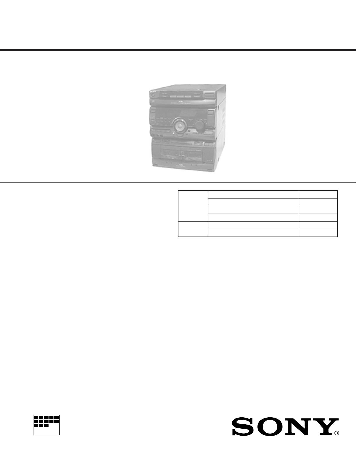
MINI Hi-Fi COMPONENT SYSTEM
CDM38L-5BD29AL
KSS-213D/Q-NP
Similar Mechanism HCD-H881
Tape player section
Recording system 4-track 2-channel stereo
Frequency response 60 – 13,000 Hz (± 3 dB),
(DOLBY NR OFF) using Sony TYPE I
cassette
60 – 14,000 Hz (± 3dB),
using Sony TYPE II
cassette
Wow and flutter ± 0.15% W. Peak (IEC)
0.1% W. RMS (NAB)
± 0.2 % W. Peak (DIN)
– Continued on next page –
MICROFILM
Page 2
Tuner section
FM stereo, FM/AM superheterodyne tuner
FM tuner section
Tuning range
AEP, UK, G, AED: 87.5 – l08.0 MHz
(50 kHz step)
EE, CIS: 65.0 – 74.0 MHz (10 kHz step)
87.5 – 108.0 MHz
(50 kHz step)
Aerial FM Lead aerial
Aerial terminals 75 ohms unbalanced
Intermediate frequency 10.7 MHz
UKV tuner section (EE, CIS)
Tuning range 65.0 – 74.0 MHz
(10 kHz step)
Polar Stereo
AM tuner section
Tuning range MW: 531 – 1,602 kHz
(with interval set at 9 kHz)
LW: 153 – 279 kHz
(with interval set at 3 kHz)
Aerial AM loop aerial
External aerial terminal
Intermediate frequency 450 kHz
General
Power requirements 220 – 230 V AC, 50/60 Hz
Power consumption 130 watts
Dimension (w/h/d) Approx. 280 × 330 × 366 mm
Mass Approx. 8.1 kg
Supplied accessories: AM loop aerial (1)
Remote RM-SD70 (1)
Sony SUM-3 (NS)
batteries (2)
FM lead aerial (1)
Speaker cords (4)
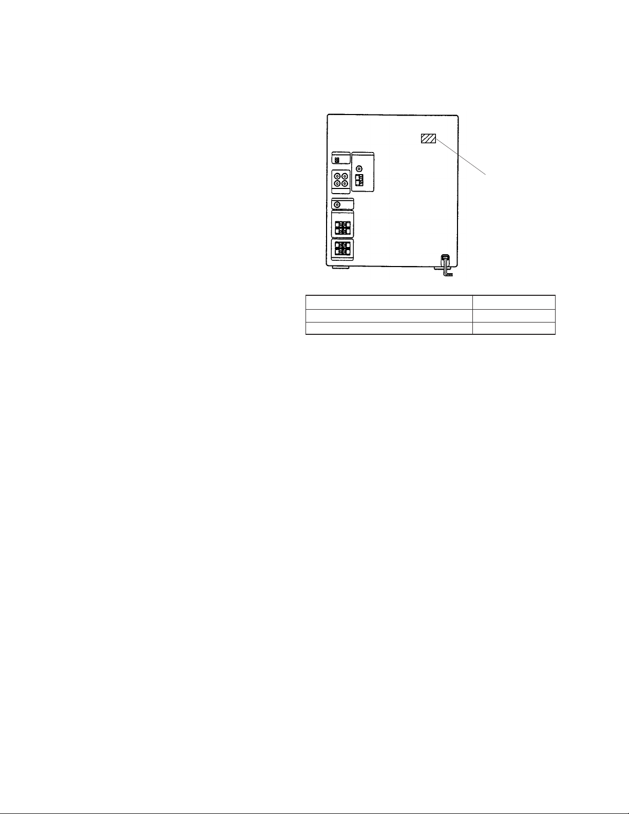
MODEL IDENTIFICATION
– BACK PANEL –
PARTS No.
MODEL PARTS NO.
AEP, UK, G, AED model 4-986-844-5π
EE, CIS model 4-986-844-6π
• Abbreviation
AED : Northern European model
G : German model
EE : East European model
Design and specifications are subject to change without notice.
– 2 –
Page 3
CAUTION
Use of controls or adjustments or performance of
procedures other than those specified herein may
result in hazardous radiation exposure.
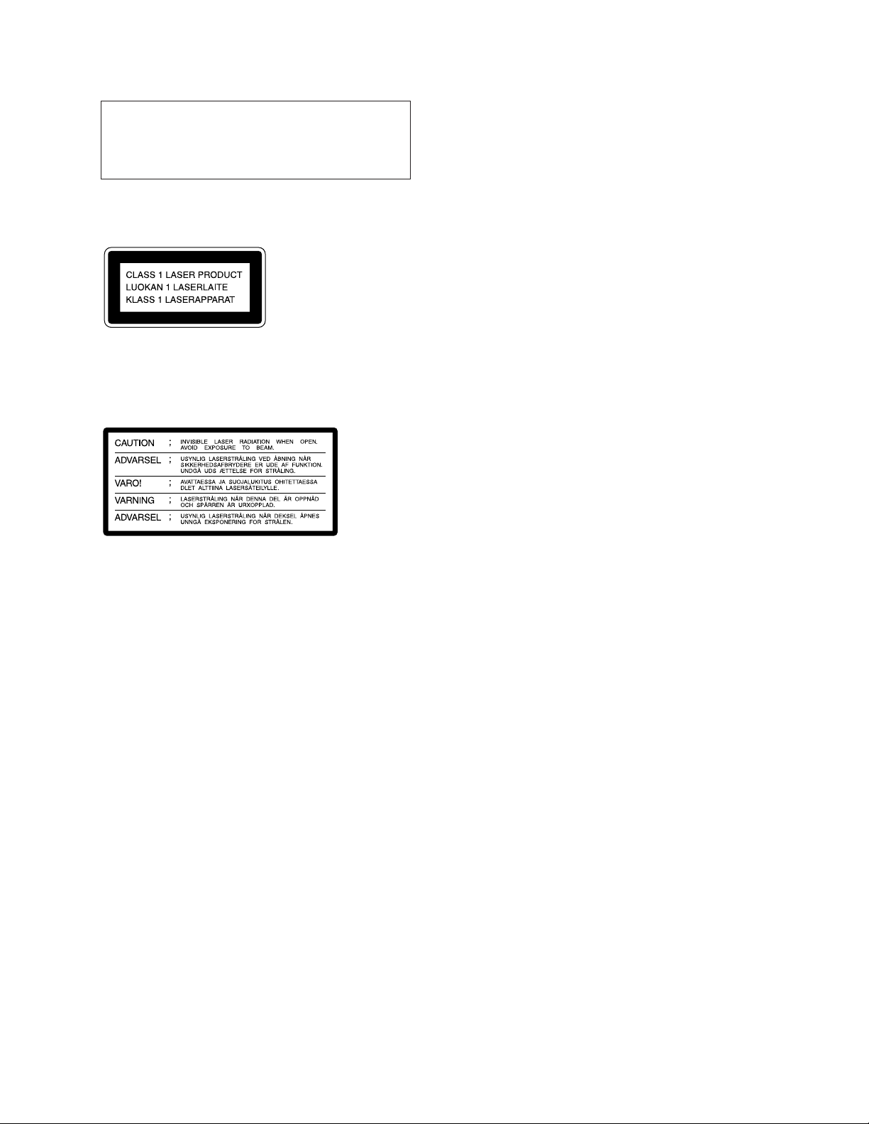
This appliance is classified as a CLASS 1 LASER product.
The CLASS 1 LASER PRODUCT MARKING is located on
the rear exterior.
Laser component in this product is capable of emitting radiation
exceeding the limit for Class 1.
The following caution label is located inside the unit.
SAFETY-RELATED COMPONENT WARNING!!
COMPONENTS IDENTIFIED BY MARK ! OR DOTTED
LINE WITH MARK ! ON THE SCHEMATIC DIAGRAMS
AND IN THE PARTS LIST ARE CRITICAL TO SAFE
OPERATION. REPLACE THESE COMPONENTS WITH
SONY PARTS WHOSE PART NUMBERS APPEAR AS
SHOWN IN THIS MANUAL OR IN SUPPLEMENTS PUBLISHED BY SONY.
– 3 –
Page 4

TABLE OF CONTENTS
Servicing Notes ........................................................................... 4
1. GENERAL ..................................................................... 5
2. DISASSEMBLY .......................................................... 22
3. TEST MODE ............................................................... 28
4. MECHANICAL ADJUSTMENTS .......................... 30
SERVICING NOTES
NOTES ON HANDLING THE OPTICAL PICK-UP
BLOCK OR BASE UNIT
The laser diode in the optical pick-up block may suffer electrostatic
break-down because of the potential difference generated by the
charged electrostatic load, etc. on clothing and the human body.
During repair, pay attention to electrostatic break-down and also
use the procedure in the printed matter which is included in the
repair parts.
The flexible board is easily damaged and should be handled with
care.
5. ELECTRICAL ADJUSTMENTS
Deck Section...................................................................... 30
Tuner Section..................................................................... 33
CD Section......................................................................... 35
6. DIAGRAMS
6-1. Printed Wiring Board –TUNER Section– ......................... 38
6-2. Schematic Diagram –TUNER Section– ............................ 40
6-3. Printed Wiring Board –CD Section– ................................. 43
6-4. Schematic Diagram –CD Section– .................................... 45
6-5. Printed Wiring Boards –CD MOTOR Section– ................ 47
6-6. Schematic Diagram –CD MOTOR Section–..................... 49
6-7. Printed Wiring Boards –DECK Section– .......................... 51
6-8. Schematic Diagram –DECK Section–............................... 53
6-9. Schematic Diagram –MAIN/POWER Section–................ 57
6-10. Printed Wiring Boards –MAIN/POWER Section–............ 61
6-11. Schematic Diagram –PANEL Section– ............................. 65
6-12. Printed Wiring Boards –PANEL Section– ......................... 69
6-13. Printed Wiring Board –POWER AMP Section– ............... 73
6-14. Schematic Diagram –POWER AMP Section– .................. 74
6-15. IC Pin Function Description .............................................. 82
7. EXPLODED VIEWS .................................................. 86
8. ELECTRICAL PARTS LIST .................................... 94
NOTES ON LASER DIODE EMISSION CHECK
The laser beam on this model is concentrated so as to be focused on
the disc reflective surface by the objective lens in the optical pickup block. Therefore, when checking the laser diode emission, observe from more than 30 cm away from the objective lens.
Notes on chip component replacement
• Never reuse a disconnected chip component.
• Notice that the minus side of a tantalum capacitor may be dam-
aged by heat.
Flexible Circuit Board Repairing
• Keep the temperature of the soldering iron around 270 ˚C during
repairing.
• Do not touch the soldering iron on the same conductor of the
circuit board (within 3 times).
• Be careful not to apply force on the conductor when soldering or
unsoldering.
– 4 –
Page 5
SECTION 1
GENERAL
This section is extracted
from instruction manual.
– 5 –
Page 6
– 6 –
Page 7
– 7 –
Page 8
– 8 –
Page 9
– 9 –
Page 10
– 10 –
Page 11
– 11 –
Page 12
– 12 –
Page 13

– 13 –
Page 14
– 14 –
Page 15
– 15 –
Page 16
– 16 –
Page 17
– 17 –
Page 18
– 18 –
Page 19
– 19 –
Page 20
– 20 –
Page 21
– 21 –
Page 22
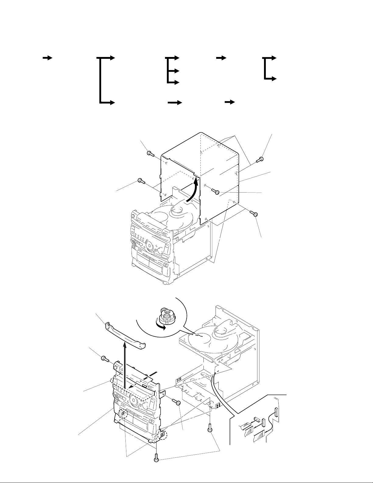
• This set can be disassembled in the order shown below.
CASE
(Page 22)
FRONT PANEL
SECTION
(Page 22)
CD MECHANISM
DECK SECTION
(Page 23)
SECTION 2
DISASSEMBLY
BASE UNIT
(Page 24)
MAIN BOARD
(Page 24)
TRAY SECTION
(Page 25)
BD BOARD
(Page 26)
OPTICAL
PICK-UP
(Page 26)
SLED
MOTOR
(Page 26)
TAPE MECHANISM
DECK SECTION
(Page 23)
Note: Follow the disassembly procedure in the numerical order given.
2
CASE
1
two screws
(case 3 TP2)
(3 × 8)
screw (case 3 TP2)
(3 × 10)
AUDIO BOARD
(Page 27)
CAPSTAN MOTOR
(Page 27)
3
three screws
(BVTT 3 × 6)
4
2
screw
(case 3 TP2)
(3 × 10)
1
two screws
(case 3 TP2)
(3 × 8)
Remove the case to
direction of the arrow.
FRONT PANEL SECTION
3
loading panel
5
screw
(BVTP 3 × 10)
2
Pull the tray
8
front panel section
7
two claws
A
1
5
screw
(BVTP 3 × 10)
Turn the cam to
direction of the
arrow A.
6
four screws
(BVTT 3 × 6)
4
three flat wires
(CN102, 205, 206)
– 22 –
Page 23
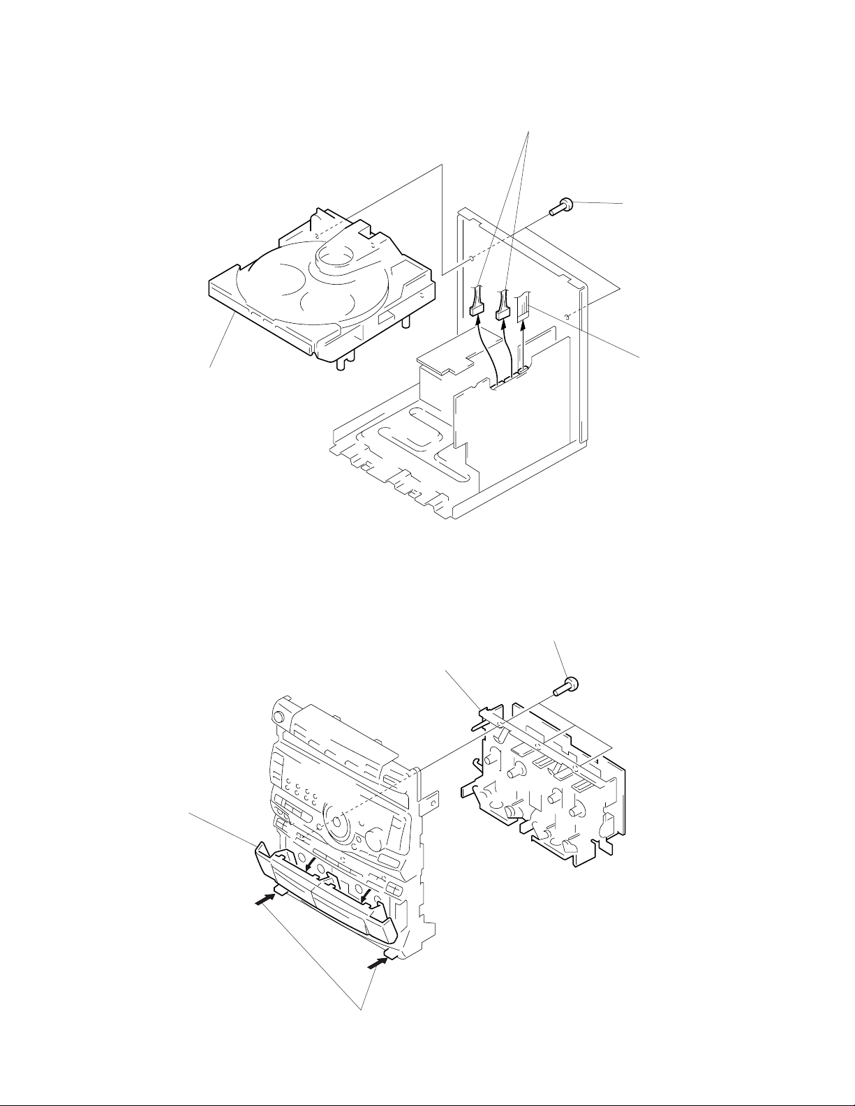
CD MECHANISM DECK SECTION
4
CD mechanism deck section
Note: The CD mechanism deck will
fall if three screws are removed.
Support it by hand, then remove
three screws.
1
two connectors
(CN203, 204)
3
two screws
(BVTP 3 × 8)
2
flat wire
(CN202)
T APE MECHANISM DECK SECTION
2
Open the
cassette lids.
4
tape mechanism deck
section
3
three screws
(BVTP 2.6 × 8)
1
Push the two buttons.
– 23 –
Page 24
BASE UNIT
1
two yoke bracket
2
boss
3
base unit
MAIN BOARD
1
connector
(CN901)
3
two screws
(BVTP 3 × 8)
3
four screws
(BVTP 3 × 8)
2
flat wire (CN201)
5
main board
IC201
– 24 –
4
connector
(CN101)
Page 25
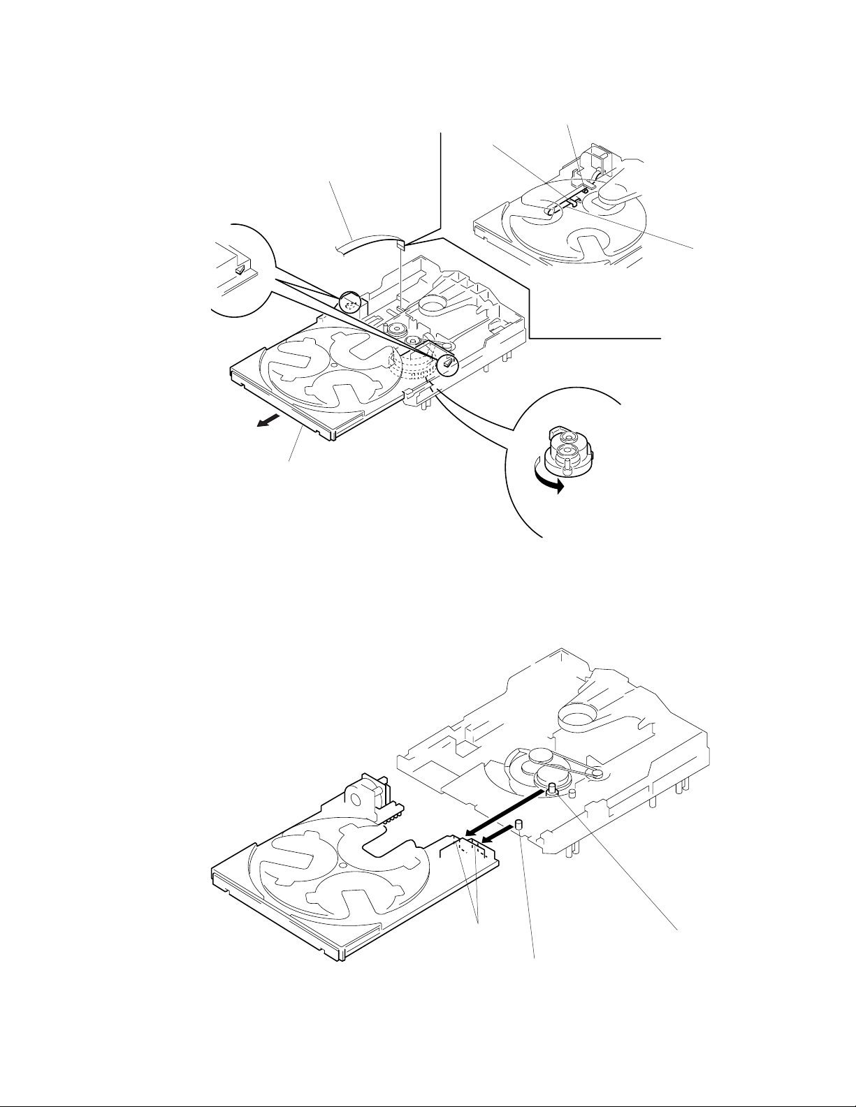
TRAY SECTION
3
flat wire
(CN705)
claw
B
claw
A
flat wire
4
two claws
2
Pull the tray.
5
Removal the tray.
Note: When installing the tray, take care so that the collars (A) and
(B) are properly inserted into the slots.
Note: When installing the tray, pull around the flat
wire to pass through the claw A and claw B,
as shown in the figure.
1
Turn the cam to direction
of the arrow.
– 25 –
slots
collar
B
collar
A
Page 26
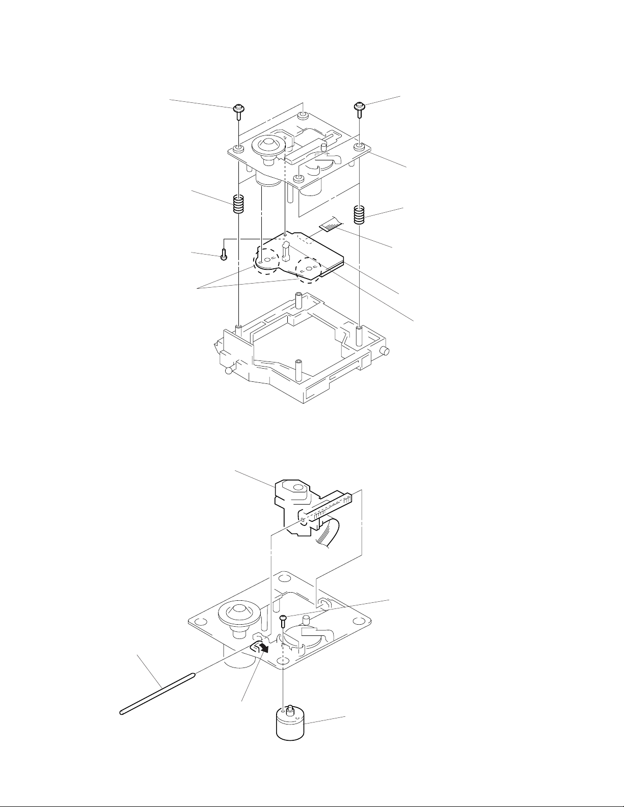
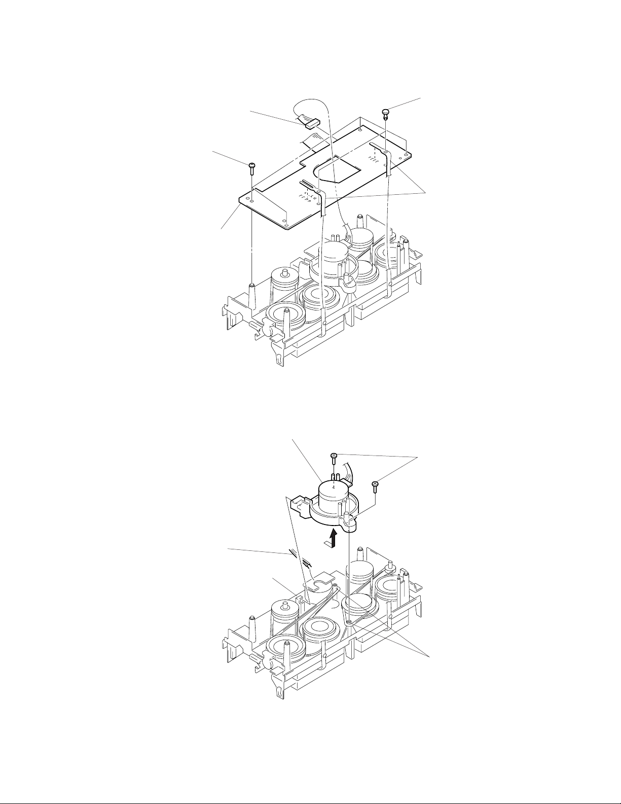
BD BOARD
1
two screws
(PTPWH M2.6 × 6)
5
screw
(BVTP 2.6 × 8)
3
two springs
6
Removal
the four solders.
1
two screws
(PTPWH M2.6 × 6)
2
optical pick-up
section
3
two springs
4
flat wire
(CN101)
7
BD board
limit switch
OPTICAL PICK-UP, SLED MOTOR
2
sled shaft
3
optical pick-up
1
claw
5
sled motor
4
two screws
(P 2 × 3)
– 26 –
Page 27
AUDIO BOARD
4
four screws
(BTP 2.6 × 4)
5
AUDIO board
1
connector
(CN651)
2
two rivets
3
Break the soldering of two
flexible flat cables.
CAPSTAN MOTOR
1
Break the soldering of
motor lead.
4
Removal the capstan motor
to direction of the arrow.
3
claw
2
two screws
(BTP 2.6 × 8)
5
Hang the
two belts.
– 27 –
Page 28

SECTION 3
TEST MODE
[MC Cold Reset]
• The cold reset clears all data including preset data stored in the
RAM to initial conditions. Execute this mode when returning the
set to the customer.
Procedure:
1. Press three buttons SPECTRUM ANALYZER ,
ENTER/NEXT , and DISC 1 simultaneously.
2. The fluorescent indicator tube becomes blank instantaneously,
and the set is reset.
[CD Delivery Mode]
• This mode moves the pickup to the position durable to vibration.
Use this mode when returning the set to the customer after repair.
Procedure:
1. Press POWER button to turn the set ON.
2. Press PLAY button and POWER button simultaneously.
3. A message “LOCK” is displayed on the fluorescent indicator
tube, and the CD delivery mode is set.
[MC Hot Reset]
• This mode resets the set with the preset data kept stored in the
memory. T he hot reset mode functions same as if the po wer cord
is plugged in and out.
Procedure:
1. Press three buttons SPECTRUM ANALYZER ,
ENTER/NEXT , and DISC 2 simultaneously.
2. The fluorescent indicator tube becomes blank instantaneously,
and the set is reset.
[Sled Servo Mode]
• This mode can run the CD sled motor freely. Use this mode, for
instance, when cleaning the pickup.
Procedure:
1. Select the function “CD”.
2. Press three buttons SPECTRUM ANALYZER ,
ENTER/NEXT , and FUNCTION simultaneously.
3. The Sled Servo mode is selected, if “CD” is blanking on the
fluorescent indicator tube.
4. With the CD in stop status, press ) button in CD section to
move the pickup to outside track, or 0 button to inside track.
5. To exit from this mode, perform as follows:
1) Move the pickup to the most inside track.
2) Press three buttons in the same manner as step 2.
Note:
• Always move the pickup to most inside track when exiting from
this mode. Otherwise, a disc will not be unloaded.
• Do not run the sled motor excessively, otherwise the gear can be
chipped.
[Change-over of AM Tuner Step between 9kHz and 10kHz]
• A step of AM channels can be changed over between 9kHz and
10kHz.
Procedure:
1. Press POWER button to turn the set ON.
2. Select the function “TUNER”, and press TUNER/BAND
button to select the BAND “AM”.
3. Press POWER button to turn the set OFF.
4. Press ENTER/NEXT and POWER buttons simultaneously,
and the display of fluorescent indicator tube changes to “AM
9k STEP” or “AM 10k STEP”, and thus the channel step is
changed over.
[LED and Fluorescent Indicator Tube All Lit, Key Check
Mode]
Procedure:
1. Press three buttons SPECTRUM ANALYZER ,
ENTER/NEXT , and DISC 3 simultaneously.
2. LEDs and fluorescent indicator tube are all turned on.
Press DISC 2 button, and the key check mode is activated.
3. In the key check mode, the fluorescent indicator tube displays
“K 1 V0 J0”. Each time a button is pressed, “K”v alue increases.
However, once a button is pressed, it is no longer taken into
account.
“J” value increases like 1, 2, 3 ... if rotating JOG knob in “+”
direction, or it decreases like 0, 9, 8 ... if rotating in “–” direction.
“V” value increases like 1, 2, 3 ... if rotating VOLUME knob
in “+” direction, or it decreases like 0, 9, 8 ... if rotating in “–”
direction.
4. To e xit from this mode, press three buttons in the same manner
as step 1, or disconnect the power cord.
[Change-over of FUNCTION Name]
• The FUNCTION name of external input terminal can be changed
over to VIDEO or MD.
Procedure:
1. Press POWER button to turn the set OFF.
2. Press POWER button together with FUNCTION button, and
the power is turned on, the display of fluorescent indicator tube
changes to “MD” or “VIDEO” instantaneously, and thus the
FUNCTION is changed over.
– 28 –
Page 29

[Aging Mode]
This mode can be used for operation check of CD section and tape
deck section.
• If an error occurred:
The aging operation stops.
• If no error occurs:
The aging operation continues repeatedly.
1. Aging Mode in CD Section
1-1. Operating Method of Aging Mode
1. Set discs in DISC1 and DISC2 trays.
2. Select the function “CD”.
3. Press three buttons SPECTRUM ANALYZER ,
ENTER/NEXT , and KARAOKE PON/MPX simulta-
neously.
4. The aging mode is activated, if a roulette mark on the fluo-
rescent indicator tube is blinking.
5. In the aging mode, the aging is executed in a sequence given
in “1-2. Operation during Aging Mode”.
The aging continues unless an alarm occurred.
6. To e xit from the aging mode, press POWER button to turn
the set OFF.
• If a button other than buttons In CD section is pressed during
aging, the aging in the CD section is finished.
• To execute aging to the tape deck section successi v ely , press ·
button in the deck A.
“ A GING” is displayed on the fluorescent indicator tube. (For the
aging in tape deck, see “2. Aging Mode in Tape Deck Section”.
1-2. Operation during aging Mode
In the aging mode, the program is executed in the following sequence.
1. The disc table is ejected.
2. The disc tray turns to select a disc. (For a disc selection
sequence, see Section 1-3.)
3. TOC of disc is read.
4. The pickup accesses to the last track.
5. A disc is ejected.
6. Steps 2 through 5 are repeated.
7. In the aging mode, the aging is executed in a sequence given
in “2-2. Operation during Aging Mode”.
The aging continues unless an alarm occurred.
8. To exit from the aging mode, press POWER button to turn
the set OFF.
2-2. Operation during Aging Mode
In the aging mode, the program is executed in the following sequence.
1. A tape on FWD side is played for one minute.
2. PAUSE STOP is made.
3. Recording is made for 3 minutes. (For the deck not having
the record function, the play is executed. In this case, ·
LED does not light up.)
4. FF is executed up to the end of tape.
5. A tape is reversed, and the tape on REV side is played for
one minute.
6. PAUSE STOP is made.
7. Recording is made for 3 minutes. (For the deck not having
the record function, the play is executed. In this case, ª
LED does not light up.)
8. FF is executed up to the end of tape.
9. Steps 1 through 8 are executed for the other deck.
10. Steps 1 through 9 are repeated unless an alarm occurred.
2-3. Deck Selection Sequence
• During the aging mode, decks are selected in the following se-
quence:
Deck A (FWD) → Deck A (REV)
↑↓
Deck B (REV) ← Deck B (FWD)
1-3. Disc Selection Sequence
• During the aging mode, discs are selected in the following se-
quence:
Disc 1 → Disc 2
↑↓
Disc 2 ← Disc 1
2. Aging Mode in Tape Deck Section
2-1. Operating Method of Aging Mode
1. Load a commercially available 10-minute tape into the decks
A and B respectively.
(If a 10-minute tape is not available, another tape may be
used but a cycle time will be longer.)
2. Select the function “TAPE”.
3. Rewind tapes in advance by pressing 0 button respectively on decks A and B.
4. Press three buttons SPECTRUM ANALYZER ,
ENTER/NEXT , and KARAOKE PON/MPX simulta-
neously.
5. Press · button on deck A. (This button trigger s the aging mode.)
6. The aging mode is activated if “AGING A” is displayed on
the fluorescent indicator tube.
– 29 –
Page 30

SECTION 4
MECHANICAL ADJUSTMENTS
SECTION 5
ELECTRICAL ADJUSTMENTS
PRECAUTION
1. Clean the following parts with a denatured-alcohol-moistened
swab:
record/playback head pinch roller
erase head rubber belts
capstan idlers
2. Demagnetize the record/playback head with a head demagnetizer.
3. Do not use a magnetized screwdriver for the adjustments.
4. After the adjustments, apply suitable locking compound to the
parts adjusted.
5. The adjustments should be performed with the rated power supply voltage unless otherwise noted.
• Tor que Measurement
Mode Torque Meter Meter Reading
Forward CQ-102C
Forward
Back Tension (0.026 – 0.082 oz•inch)
Reverse CQ-102RC
Reverse
Back Tension (0.026 – 0.082 oz•inch)
FF, REW CQ-201B
CQ-102C
CQ-102RC
36 to 61 g•cm
(0.50 – 0.84 oz•inch)
2 to 6 g•cm
36 to 61 g•cm
(0.50 – 0.84 oz•inch)
2 to 6 g•cm
61 to 143 g•cm
(0.85 – 1.98 oz•inch)
DECK SECTION 0 dB=0.775 V
1. Demagnetize the record/playback head with a head demagnetizer. (Do not bring the head demagnetizer close to the erase
head.)
2. Do not use a magnetized screwdriver for the adjustments.
3. After the adjustments, apply suitable locking compound to the
parts adjust.
4. The adjustments should be performed with the rated power supply voltage unless otherwise noted.
5. The adjustments should be performed in the order given in this
service manual. (As a general rule, playback circuit adjustment
should be completed before performing recording circuit adjustment.)
6. The adjustments should be performed for both L-CH and R-ch.
7. Switches and controls should be set as follows unless otherwise
specified.
8. Set to test mode. (Press key switch same time
SPECTRUM ANALYZER ENTER/NEXT and
EFFECT ON/OFF button.)
• Test Tape
Tape Signal Used for
P-4-A100 10 kHz, –10 dB Azimuth Adjustment
WS-48B 3 kHz, 0 dB Tape Speed Adjustment
P-4-L300 315 Hz, 0 dB Level Adjustment
• Tape T ension Measurement
Mode Tension Meter Meter Reading
Forward CQ-403A more than 100 g (3.53 oz)
Reverse CQ-403R more than 100 g (3.53 oz)
Record/Playback Head Azimuth Adjustment
DECK A DECK B
Note: Perform this adjustments for both decks
Procedure:
1. Mode: Playback (FWD)
test tape
P-4-A100
(10 kHz, –10 dB)
set
main board
CN207
Pin
1
(L-CH)
Pin
3
(R-CH)
main board
CN207
Pin
2
level meter
+
–
– 30 –
Page 31

2. Turn the adjustment screw and check output peaks. If the peaks
do not match for L-CH and R-CH, turn the adjustment screw
so that outputs match within 1dB of peak.
output
level
within
1dB
L-CH
peak
R-CH
peak
within
1dB
Screw
position
L-CH
peak
Screw
position
R-CH
peak
Tape Speed Adjustment DECK A
Note: Start the Tape Speed adjustment as belo w after setting to the
test mode.
In the test mode, the tape speed is high during pressing the
HIGH SPEED DUBBING button.
Procedure:
1. Turn the power switch on.
2. Press the SPECTRUM ANALYZER button,
ENTER/NEXT button and EFFECT ON/OFF button simul-
taneously.
To exit from the test mode, press the POWER button.
Mode: Playback (FWD)
test tape
WS-48B
(3 kHz, 0 dB)
frequency counter
3. Mode: Playback (FWD)
test tape
P-4-A100
(10 kHz, –10 dB)
L-CH
main
board
CN207
set
R-CH
waveform of oscilloscope
in phase 45°90°135°180
pin
L
R
pin
good
1
pin
3
2
oscilloscope
V
wrong
H
°
4. Repeat steps 1 to 3 in playback (REV) mode.
5. After the adjustments, apply suitable locking compound to the
pats adjusted.
Adjustment Location: Record/Playback Head (Deck A and B)
and main board.
1
: L-CH)
3
:R-CH)
+
–
set
main board
CN207 (Pin
(Pin
1. Insert the WS-48B into the deck A and the blank tape into the
deck B.
2. Press the REC button and · button on the deck B. Then
the deck B is at recording mode.
3. Set the deck A to playback mode.
4. Keep pressing the HIGH SPEED DUBBING button in playback mode.
Then at HIGH speed mode.
5. Adjust RV652 on the AUDIO board do that frequency counter
reads 6,000 ± 60 Hz.
6. Take off the HIGH SPEED DUBBING button.
Then at NORMAL speed mode.
7. Adjust RV651 on the AUDIO board so that frequency counter
reads 3,000 Hz.
+30
–10
8. Frequency difference between deck A and deck B the beginning
of the tape should be within ± 1.5%.
Adjustment Location: AUDIO board
Playback level Adjustment DECK A DECK B
Procedure:
Mode: Playback (FWD)
forward
reverse
test tape
P-4-L300
(315 Hz, 0 dB)
set
main board
CN207 (Pin
(Pin
level meter
1
: L-CH)
3
: R-CH)
+
–
Deck A is RV311 (L-CH) and RV411 (R-CH), Deck B is RV301 (LCH) and R V401 (R-CH) so that adjustment within adjustment le vel
as follows.
Adjustment Level:
CN207 PB level: 301.5 to 338.3 mV (–8.2 to –7.2 dB) level
difference between the channels: within ±0.5 dB
Adjustment Location: AUDIO and main boards
– 31 –
Page 32

Record bias Current Adjustment DECK B
5
Procedure:
1. Mode: Record
Adjustment Location: Main board
[MAIN BOARD] (Component Side)
Pin 6 (L-CH) of IC1501 on the main board.
#¶
(L-CH) of IC1501 on the main board.
Pin
1) 315 Hz
2) 10 kHz
AF OSC
attenuator
Pin 2 (GND) of ICN207 on the main board.
50 mV (–23.8 dB)
Ω
600
set
blank tape
CN-123
2. Mode: Playback
recorded
portion
set
CN207 (Pin
(Pin
level meter
1
: L-CH)
3
: R-CH)
+
–
Confirm playback the signal recorded in step 1 become adjustable
limits as follows.
If these levels do not adjustable limits, adjustment the R V341 (L-CH)
and RV441 (R-CH) on the AUDIO board to repeat steps 1 and 2.
Adjustable limits: Playback output of 315 Hz to playback output
of 10kHz: ±0.5 dB
Adjustment Location:AUDIO and main boards
Record Level Adjustment DECK B
Procedure:
1. Mode: Record
Pin
6
(L-CH) of IC1501 on the main board.
Pin
#¶
(R-CH) of IC1501 on the main board.
AF OSC
315 Hz, 50 mV (–23.8 dB)
Ω
attenuator
600
blank tape
CS-123
set
IC201
IC301
[AUDIO BOARD] (Conductor Side)
RECORD
BAIS
L
RV301
®
RV401
®
PB LEVEL
– DECK B –
R
L
RV441RV341
R
(NORMAL)
RV1501
IC1501
CN207
RV1551
RECORD LEVEL
TAPE SPEED
RV651
®
PB
LEVEL
– DECK A –
(HIGH)
RV652
RV311
RV411
R
®
L
®
®
CN20
Pin
2
(GND) of CN207 on the main board.
2. Mode: Playback
recorded
portion
set
CN207 (Pin
(Pin
level meter
1
: L-CH)
3
: R-CH)
+
–
Confirm playback the signal recorded in step 1 become adjustable
limits as follows.
If these levels do not adjustable limits, adjustment the RV1501 (LCH) and R V1551 (R-CH) on the main board to repeat steps 1 and 2.
Adjustable limits:
CN207 PB level: 47.3 to 53.1 mV (–24.3 to –23.3 dB)
– 32 –
Page 33

TUNER SECTION 0 dB=1 µV
Note: As a front-end (FE1) is difficult to repair if faulty, replace it
with new one.
AM Section Adjustment
Setting:
loop antenna
(Supplied accessories)
µ
V/m) =SSG output level dB (µV/m) –26 dB.
AM RF SSG
30% amplitude
modulation by
400 Hz signal
loop antenna
60 cm
Field strength dB (
AM Tuned Level Adjustment
Band: AM or MW
Procedure:
1. Set the output of SSG so that the input level of the set becomes
55 dB.
2. Tune the set to 999 kHz.
3. Adjust RV41 to the point (moment) when the TUNED indicator
will change from going off to going on.
Adjustment Location : TCB board
FM Section Adjustment
Note: This adjustment should be performed after the AM Tuned
Level Adjustment due to the same adjustment element.
Setting:
set
AM ANTENNA
terminal (TM1)
Adjustment Location:
[TCB BOARD] (Component Side)
IC41
RV42
RV41
TM1
FM RF stereo signal
generator
Ω
coaxial
75
set
Carrier frequency : 98 MHz
Modulation : AUDIO 1 kH, 75 kHz
deviation (100%)
FM ANTENNA terminal
(TM1) (75
Ω
open)
FM Tuned Level Adjustment
Band: FM
Procedure:
1. Supply a 25 dBµ 98 MHz signal from the ANTENN A terminal.
2. Tune the set to 98 MHz.
3. If the TUNED indicator does not light, adjust R V42 to the point
(moment) when the TUNED indicator will change from going
off to going on.
Adjustment Location: TCB board
FE1
– 33 –
Page 34

FM Polar Adjustment (EE, CIS model only)
Connection 1:
FM RF SSG
Ω
coaxial
75
set
FM ANTENNA terminal
(75
Ω
)
Carrier frequency: 69 MHz
Output level : 1 mV (60 dBµ) (at 75 Ω open)
Modulation : AUDIO 1 kHZ, 10 kHz deviation
Connection 2:
AF OSC
FM RF SSG
Ω
coaxial
75
Audio 31.25 kHz
external
modulation
terminal
FM ANTENNA terminal
(75
Ω
)
Procedure :
1. Set the modulation of FM RF SSG to AUDIO 1 kHz, 10 kHz
deviation according to "Connection 1".
2. Tune the set to 69 MHZ.
3. Adjust the RV1702 so that the reading of frequency counter
connected to TP1702 becomes within 31.25 kHz ± 0.05 kHz.
(VCO adjustment)
4. Then record the reading of the level meter connected to TP1701
5. Set the modulation of FM RF SSG to AUDIO 31.25 kHz, 10
kHz deviation according to "Connection 2".
6. Tune the set to 69 MHz.
7. Set the CT1701 to be mechanical center.
8. Adjust the L1701 so that the reading of the level meter connected to TP1701 become maximum.
Then adjust the CT1701 so that the reading of the level meter
connected to TP1701 becomes maximum. (SUB CARRIER
PEAK Adjustment)
9. Adjust the RV1701 so that the level at the moment becomes 14
dB higher value than the level recorded in step 4. (SUB CARRIER LEVEL Adjustment)
set
Carrier frequency: 69 MHz
Output level : 1 mV (60 dBµ) (at 75 Ω open)
Modulation : AUDIO 31.25 kHZ, 10 kHz deviation
(EXTERNAL MODULATION)
Adjustment Location :
EE, CIS model :
[TCB BOARD] (Component Side)
• Abbreviation
EE: East European model
RV41
AM tuned level
Adjustment
R V1701, TP1701
Sub carrier level
Adjustment
CT1701, L1701, TP1701
Sub carrier peak
Adjustment
RV41
IC41
L1701
(FILTER) TP1701
RV1702, TP1702
VCO Adjustment
RV42
TM1
IC1701
RV1702
RV1701
CT1701
TP1702
(VCO)
FE1
R V42
FM tuned level
Adjustment
LEVEL METER
+
–
FREQUENCY COUNTER
+
–
– 34 –
Page 35

CD SECTION
+
–
BD board
TP (FEO)
TP (VC)
oscilloscope
A
B
symmetry
within 3
±
1 Vp-p
VOLT/DIV: 200 mV
TIME/DIV: 500 ns
level:
1.3
±
0.3 Vp-p
+
–
BD board
TP (RF)
TP (VC)
oscilloscope
Note:
1. CD Block is basically designed to operate without adjustment.
Therefore, check each item in order given.
2. Use YEDS-18 disc (3-702-101-01) unless otherwise indicated.
3. Use an oscilloscope with more than 10M impedance.
4. Clean the object lens by an applicator with neutral detergent
when the signal level is low than specified value with the following checks.
5. Adjust the focus bias adjustment when optical block is replaced.
Focus Bias check
oscilloscope
(DC range)
BD board
TP (RF)
VC
+
–
Procedure:
1. Connect oscilloscope to test point TP (RF). (GND terminal :
VC)
2. Turned Power switch on.
3. Put disc (YEDS-18) in and playback.
4. Confirm that the shape “≈” can be clearly distinguished at the
center of the waveform and check the RF signal level.
• RF signal
VOLT/DIV: 200 mV
TIME/DIV: 500 ns
S Curve Check
Procedure:
1. Connect oscilloscope to test point TP (FEO).
2. Connect between test point TP (FOK) and GND by lead wire.
3. Turn Power switch on.
4. Put disc (YEDS-18) in and turned Power switch on again and
actuate the focus search. (actuate the focus search when disc
table is moving in and out.)
5. Check the oscilloscope waveform (S-curve) is symmetrical between A and B. And conf irm peak to peak level within 3±1 Vp-p.
S-curve waveform
6. After check, remove the lead wire connected in step 2.
Note: • Try to measure several times to make sure than the ratio of
A : B or B : A is more than 10 : 7.
• T ake sweep time as long as possible and light up the brightness to obtain best waveform.
RF Level Check
level:
1.3
±
0.3 Vp-p
Procedure:
1. Connect oscilloscope to test point TP (RF) on BD board.
2. Turned Power switch on.
3. Put disc (YEDS-18) in and playback.
4. Confirm that oscilloscope waveform is clear and check RF signal level is correct or not.
Note:
Clear RF signal waveform means that the shape “≈” can be
clearly distinguished at the center of the waveform.
• RF signal
– 35 –
Page 36

E-F Balance (1 Track Jump) check
)
(Without remote commander)
oscilloscope
BD board
TP (TEO)
TP (VC)
+
–
Procedure:
1. Connect oscilloscope to test point TP (TEO) on BD board.
2. Turned Power switch on.
3. Put disc (YEDS-18) in to play the number five track.
4. Press the “P (Pause)” button. (Becomes the 1 track jump mode)
5. Check the level B of the oscilloscope's wav eform and the A (DC
voltage) of the center of the Traverse waveform.
Confirm the following:
A – B
2 (A + B)
1 track jump waveform
× 100 = ±7 (%)
Adjustment Location:
[BD BOARD] (Conductor Side)
RF
FOK
IC101
CNU101
TEO
GND
FEO
IC103
VC
IC
I02
GND
0V
level : 500 mV
±
100 mVp-p
Center of the waveform
B
A (DC voltage
symmetry
CNU102
– 36 –
Page 37

• Circuit Boards Location
SECTION 6
DIAGRAMS
TRANS board
CD SW board
PANEL board
HP/MIC board
DECO board
TC SW board
TCB board
MAIN board
POWER AMP board
MOTOR board
SENSOR board
MOTOR (TURN) board
CONNECTOR board
BD board
MOTOR (SLIDE) board
LEAF SWITCH board
AUDIO board
– 37 –
Page 38

Page 39

Page 40

• Waveforms
V
V
V
V
1 IC101 #£ pin (RF_O)
6 IC103 ^™ pin (RFCK)
2 IC101 2 pin (FEI)
3 IC101 $¶ pin (TEI)
1.3 ±0.3 Vp-p
0.1
5.6 V
135.5 µsec
7 IC103 &¢ pin (WFCK)
5.6 V
135.5 µsec
8 IC103 *ª pin (XTAI)
4 IC103 @¶ pin (MDP)
7.8 µsec
5 IC103 ^º pin (XPCK)
0.2
2.4
7
10 V
59.8 nsec
230 nsec
– 42 –
Page 41

Page 42

Page 43

Page 44
Page 45

Page 46

Page 47

Page 48

Page 49

Page 50

Page 51

Page 52

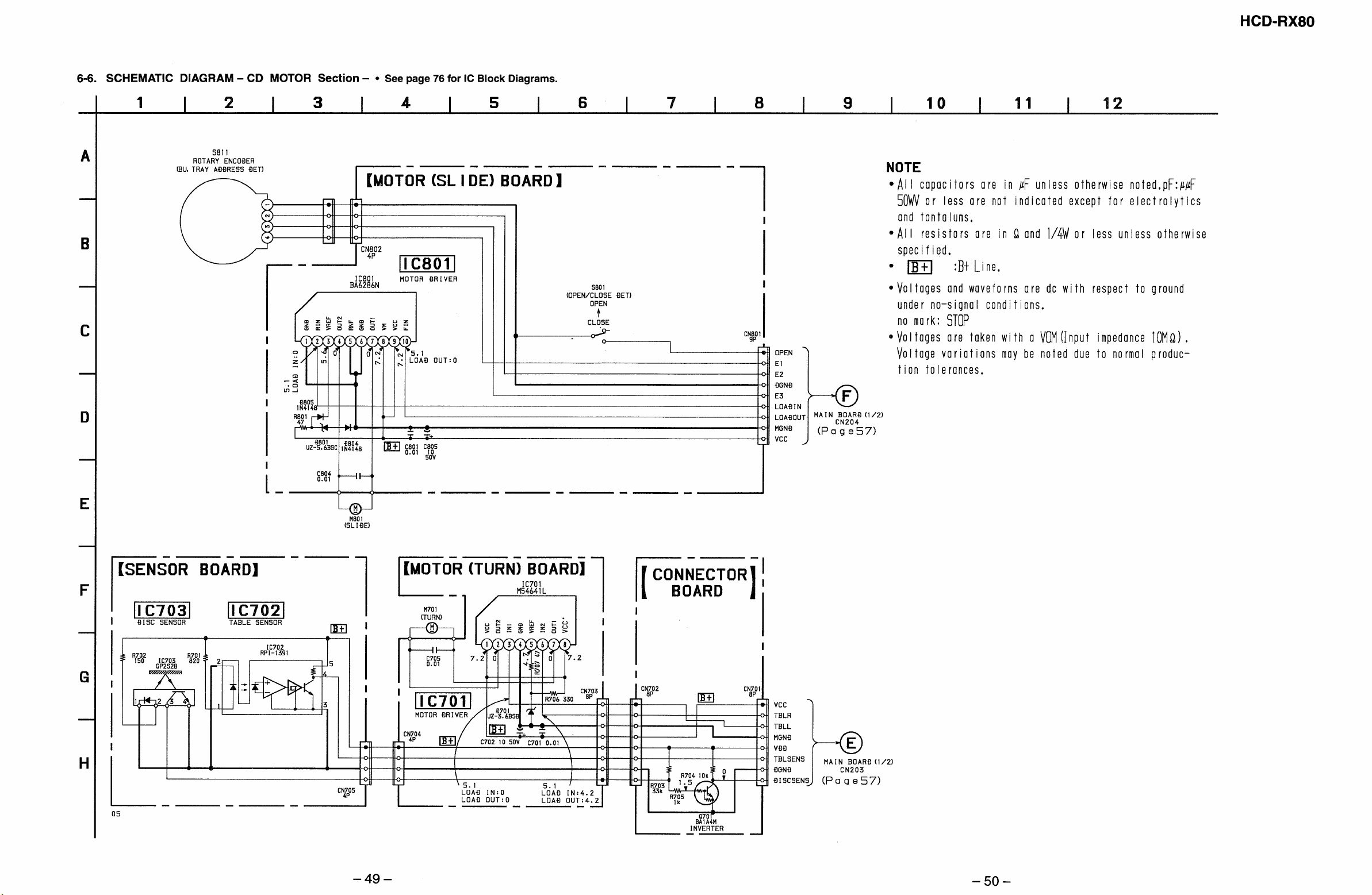
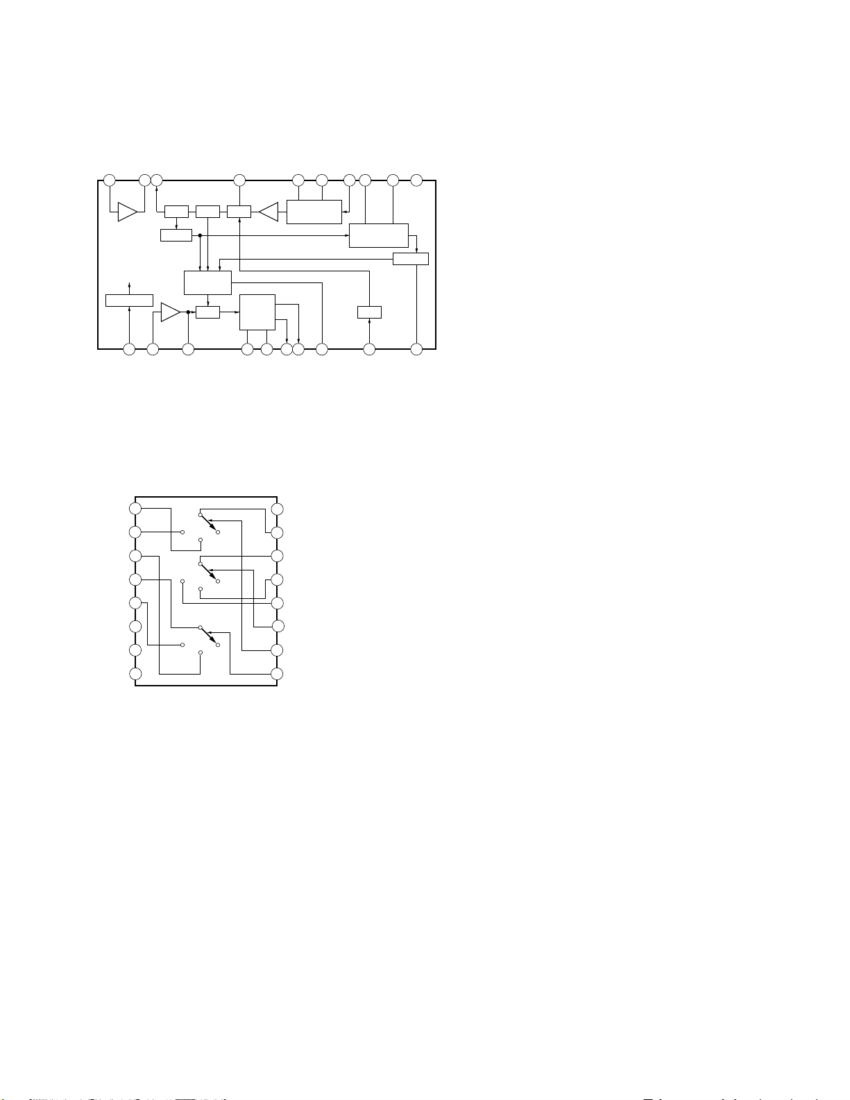
• IC Block Diagrams
IC21 LC72130 (TCB BOARD)
XOUT
VSS
AOUT2
AIN2
21222324
PD2
20
PHASE DETECTOR
CHARGE PUMP
PD1
AIN1
AOUT1
VDD
19 18 17 16 15 14
FMIN
AMIN
IO2
13
IC41 LA1835 (TCB BOARD)
UNLOCK
DETECTOR
REFERENCE
DIVIDER
2
B
C
I/F
2 345 6 7 8 9 10
1
CL
CE
D0
BO5
D1
XIN
SWALLOW COUNTER
1/16, 1/17 4BITS
12BITS PROGRAMMABLE
DRIVER
DATA SHIFT REGISTER LATCH
BO1
BO2
POWER
ON
RESET
BO3
BO4
1/2
UNIVERSAL
COUNTER
1211
IO1
IFIN
FM-SD
ALC
BUFF
LEVEL
DET
FM
IF
1
S METER
FM-IN
AM-OSC
AM
OSC
S-CURVE
FM
DET
FM-AFC
AM
MIX
2 3
AM-RF-IN
AGC
AM. CUT
AM
RF. AMP
AGC
FMIFAM
DET
AM/FM
BUFF
IF
AM-MIX
COMP
IF
TUNING
AM
DRIVE
AM-IF
GND
FM
GND
REG
5 6 7 8 9 10
4
REG
– 76 –
AM/FM
TU-LED
VCO
AM/FM
ST-LED
SW
DET
MPX-IN
VCC
VCC
OUT R
OUT L
20 19 18 17 16
21222324252627282930
DECODER
ANTI BIRDIE
STEREO
AM. SD
SW
TRIG
PILOT
DET
AM. SD
FF
VCO
STEREO
DRIVE
PHASE
DET
IF-BUFF
FF FF
AMP-IN R
AM/FM
AMP-IN LRL
MUTE
1514131211
VCO-STOP
Page 53
IC1701 IR3R42 (TCB BOARD)
SUBIN
SUBOUT
AMP
1
VCC
MON
1/2
PHASE
AMP
2 3
IN
WAVEFORM
SEP.
GATE
POUT
20 19 18 17 16 15 14 13 12 11
REGULATOR
VCO
OSC
1/2
SAMPLE
& HOLD
BUFFER
4
RHC
LPF1A
LPF1B
DETIN
AMP
PHASE
COMPARATOR
COMPARATOR 2
5 6 7 8 9
ROUT
LOUT
ST
LHC
LPF2A
PHASE
MUTE
LPF2B
TRIGGER
VCO STOP
IC1702 MC14053BCP (TCB BOARD)
VDD
16
B.COM
15
14
A.COM
13
A1
A0
12
11
A
10
B
C
9
C.COM
INH
VEE
VSS
1
B1
B0
2
C1
3
4
5
CO
6
7
8
OPEN
OPEN
OPEN
GND
10
LAMP
– 77 –
Page 54

IC101 CXA1992AR (BD BOARD)
FE_BIAS
LPFI
ATSC
TDFCT
PD2
PD1
CC2
CB
RF_M
LD
PD
RFTC
RF_O
RF_I
CP
CC1
FOK
27282930313233343536373839
VEE
+
–
+
–
–
+
RF SUMMING
AMP
FOH
FOL
TGH
TGL
BALH
BALL
ATSC
TZC
FZC
+
–
–
+
–
+
–
–
+
+
–
–
+
VEE
LEVEL S
VCC
–
+
VCC
–
+
VEE
–
+
MIRR
FOK
LDON
LPCL
LPC
TGFL
IIL DATA REGISTER
INPUT SHIFT REGISTER
ADDRESS DECODER
SENS SELECTOR
OUTPUT DECODER
DFCTO
IFB1-6
BAL1-4
TOG1-4
+
+
–
VCC
–
+
–
VEE
+
+
DFCT
–
+
MIRR
IIL
↓
TTL
DFCT1
CC1
FS1-4 TG1-2 TM1-7 PS1-4
SENS2
26
IIL
↓
TTL
–
TTL
↓
IIL
VCC
ISET
VCC VCC
SENS1
25
24
C. OUT
XRST
23
22
DATA
21
XLT
CLK
20
LOCK
19
VCC
18
ISET
17
SL_O
16
TM4 TM6
SL_M
VCC
FS1
FS2
Charge
up
TM7
TM3
TM5
VEEVEE
FSET
TG2
–
+
15
–
SL_P
14
+
TM2
–
+
PD2 IV
AMP
40
F
41
E
42
43
EI
44
VEE
TEO
45
46
47
TEI
48
49
TZC
50
51
VC
FZC
52
–
+
F IV AMP
–
+
E IV AMP
BAL1
BAL2
BAL3
BAL4
VEE
TOG4
TOG3
TOG2
TOG1
+
–
–
+
–
+
ATSC
WINDOW
COMP.
–
+
TZC COMP.
VCC
+
–
VCC
VEE
+
–
+
PD1 IV
AMP
TGFL
–
+
+
–
E-F BALANCE
WINDOW COMP.
+
–
–
DFCT
VCC
TM1
VCC
VEE
IFB1
+
–
IFB2
APC
–
+
IFB3
+
–
+
–
VEE
LASER POWER CONTROL
FE AMP
IFB4
IFB5
IFB6
+
–
TRK. GAIN
WINDOW COMP.
+
–
TG1
FOCUS
PHASE COMPENSATION
–
+
+
–
FO. BIAS
WINDOW
COMP.
TRACKING
PHASE COMPENSATION
DFCT
FZC COMP.
FS4
VEE
1
2 3
FEI
FEO
4
FDFCT
5 6 7 8 9 10
FGD
FLB
FE_O
FE_M
SRCH
TGU
131211
TG2
FSET
TA_M
TA_O
– 78 –
Page 55

IC102 BA5941FP-E2 (BD BOARD)
IN4B
IN4A
IN3B
IN3A
27
28
26
25
OP OUT
24
OP IN (–)
23
OP IN (+)
22
GND
21 20
NC
VCC
OUT3A
18
19
OUT3B
1617
OUT4A
OUT4B
15
NC
+
–
Vcc
–
+
–
+
–
+
–
+
–
+
+
–
1 2
VCC
BIAS IN
3
IN1B
IC103 CXD2519Q (BD BOARD)
SYSM
VDD
VSS
80
79 78
81
NC
82
AVSS
83
AVDD
84
AOUT1
85
AIN1
LOUT1
AVSS
XVDD
XTAI
XTAO
XVSS
AVSS
LOUT2
AIN2
AOUT2
AVDD
AVSS
XRST
86
87
88
89
90
91
92
93
94
95
96
97
98
NC
99
NC
100
–
+
–
+
SERIAL-IN
INTERFACE
TIMING
LOGIC
4
IN1A
EXCK
SBSO
SCOR
76 75 74
77
–
+
–
+
OVER SAMPLING
DIGITAL FILTER
6
5
IN2B
IN2A
WFCK
EMPHI
EMPH
71
73 72
PWMPWM
3RD-ORDER NOISE SHAPER
CPU
INTERFACE
DOUT
–
+
+
–
C4M
69 68
70
7
GND
FSTT
XTSL
67
EFM
DEMODURATOR
SUB CODE
PROCESSOR
MNT0
MNT1
66 65 64
8
GND
MNT3
MUTE
9
XROF
C2PO
63 62
SERVO
AUTO
SEQUENCER
MUTE
RFCK
VccVcc
10
VCC
GFS
XPCK
60
61
ERROR
CORRECTOR
16K RAM
XUGF
59 58
LEVEL SHIFT
LEVEL SHIFT
+
–
11
OUT2A
GTOP
VDD
57
DIGITAL OUT
VSS
BCKI
56 55 54
D / A
INTERFACE
+
–
12 13
OUT2B
BCK
PCMDI
PCMD
53 52 51
DIGITAL CLV
LEVEL SHIFT
LEVEL SHIFT
+
–
OUT1A
LRCKI
+
14
ASYMMETRY
CORRECTOR
DIGITAL
PLL
OSC
CLOCK
GENERATOR
–
OUT1B
LRCK
50
WDCK
49
48
ASYE
47
ASYO
46
ASYI
45
BIAS
44
RF
AVDD
43
42
CLTV
AVSS
41
40
FILI
FILO
39
38
PCO
37
VCTL
36
V16M
35
VCKI
34
VPCO1
33
VPCO2
32
TES1
31
TES0
1 234
VSS
VDD
LMUT
56789 10
TES2
CKOUT
SQCK
RMUT
SQSO
SENS
DATA
12 13
11
XLAT
CLOK
SEIN
14
CNIN
15 16 17
XLTO
DATO
CLKO
18 19
SPOA
20
SPOB
SPOC
21
SPOD
22 23
XLON
FOK
24
VDD
25 26 27
VSS
MON
28 29 30
MDP
MDS
LOCK
PWMI
– 79 –
Page 56

IC281 µPC1237HA (MAIN BOARD)
OVER LOAD DET
OFFSET DET
LATCH/
AUTORESET
1 2 3
F/F
AC OFF
DET
4 5 6 7 8
IC602 µPC1330HA (AUDIO BOARD)
INVERTER
COMPARATER
2
1
SW R1 GND SW P1
4
3
CONT
GND
5
VCC
6
SW P2 GND
CC
ON
V
MUTE
7 8 9
SW R2
IC801 BA6286N
(MOTOR (SLIDE) BOARD)
TSD
POWER
SAVE
CONTROL
LOGIC
1
GND
2
RIN
VREF
3
4
OUT2
5
RNF
GND
6
7
OUT1
VM
V
CC
VCC
FIN
8
9
10
IC701 M54641L
(MOTOR (TURN) BOARD)
VCC
1
2
OUT2
REG
IN1
GND
INPUT
3
AMP.
INPUT
AMP.
4
CONTROL
POWER AMP.
POWER AMP.
VCC
8
OUT1
7
IN2
6
REFERENCE
5
– 80 –
Page 57

IC901 LA5617 (MAIN BOARD)
CURRENT
ON/OFF
LIMITER
VMUTE VCC
VREF
VCC
ERROR
AMP
2 3
VCC
CN1
4
EN
1
VO1
CURRENT
LIMITER
5 6 7 8 9
GND
EN DISPLAY
ON/OFF
140uA
~_
COMPARATER
VREF
~_
1.8V
NC
CN2
ERROR
AMP
IC1502 LB1641 (MAIN BOARD)
T.S.D O.C.P
MOTOR
DRIVE
START
CIRCUIT
VREF
OVER HEAT
PROTECT
VEE
10
VO2
MOTOR
DRIVE
FWD/REV/STOP
CONTROL LOGIC
2 3
1
GND
DRIVE
MOTOR
NOISE
FILTER
5 6 7 8 9 10
4
VCC 1
FWD.IN
REV.IN
CLAMP
VCC 2
NOISE
FILTER
DRIVE
MOTOR
– 81 –
Page 58

6-15. IC PIN FUNCTION DESCRIPTION
MAIN BOARD IC301 µPD780018YGF-015-3BA (MASTER CONTROL)
Pin No. Pin Name I/O Function
1 TA-MUTE O Line mute signal output
2 DBFB-H/L O DBFB H/L select signal output
3 427-LAT O Latch signal output for IC201 (M62427FP)
4 K-CON-LAT O
5 K-CON-ON O
6 F-RELAY O Front speaker relay control output
7 R-RELAY O
8 PL-RELAY O
9 TEST I Connected ground
10 X2 O
11 X1 I
12 VDD – Power supply (+5V)
13 XT2 O
14 XT1 I
15 RESET I Reset signal input
16 (INT/IN) I
17 (INT/IN/OUT) I
18 SCOR O Subcode data request signal output
19 SOFT-TEST O Software test port
20 AC-CUT I Back up signal input (Not used )
21 RDS-INT I Connected ground
22 RDS-DATA I Not used
23 VDD – Power supply (+5V)
24 AVDD I Analog reference voltage input
25 ADJ I CD adjust point port
26 A-SHUT I A Deck reel pulse detector
27 B-SHUT I B Deck reel pulse detector
28 B-HALF I Half detector signal input
29 CLK-CHECK I Connected ground
30 SPEC-IN I Version select signal input
31 ADJ 2 I Connected ground
32
DEMO-MODE
33 AVSS – Ground
34 SQ-DATA-IN I Subcode Q data clock input
35 — – Not used
36 SQ-CLK I Sub code Q data clock input
37 SW-ON/OFF O Not used
38, 39 FUNC 1, 2 I Connected ground
40 VSS – Ground
41 VOL-LAT O
42 PL-LAT O
43 COM-DIN I Connected ground
44 COM-DOUT O Common serial data output
Not used
Not used
X'tal (5MHz)
X'tal (32.768 kHz)
Connected ground
I DEMO H/L select signal input
Not used
– 82 –
Page 59

Pin No. Pin Name I/O Function
45 COM-CLK O Common serial clock output
46 CD-POWER O CD power on signal output
47 CD-DATA O CD data output
48 CD-CLK O CD clock output
49 MSM-CND O Not used
50 MSM-BUSY I Connected ground
51 MSM-LAT O
52 MSM-NAR I Not used
53 MSM-CH O
54
INPUT-CHANGE
55 1IC-DATA O Data output for IC601
56 1IC-CLK O Clock output for IC601
57 XRST O CD reset signal output
58 XLT O CD latch signal output
59 FOUCUS-SW O Focus switching signal output
60 TBL-L O
61 TBL-R O
62 TRAY-LED O CD tray LED ON/OFF output
63 LOAD-OUT O
64 LOAD-IN O
65 ST-CLK O Tuner clock output
66 ST-DIN I Tuner data input
67 ST-DOUT O Tuner data output
68 ST-CE O Tuner chip enable output
69 TUNED I Tuned detection for tuner
70 STEREO I Stereo detection for tuner
71 VSS – Ground
72 ST-MUTE O Tuner mute signal output
73 SENS2 I
74 SENS I
75 DISC-SENS I Not used
76 T-SENS I CD table detection signal input
77 UPSW I Up SW (S201) signal input (Not used)
78 ENC 3 I
79 ENC 2 I Disctray address detect encoder input
80 ENC 1 I
81 OUT-OPEN I Out switch signal input
82 CAP-H/N O Capstan motor H/N speed select signal output
83 B-TRG O Trigger motor control output
84 A-TRG O Trigger motor control output
85 TRG-LOW O Trigger motor control output
86
CAP-M-ON/OFF
87 PB-A/B O PB Deck A/Deck B select output
O GAIN control output
Table motor control output
Loading motor control signal output
BD Condition signal input
O Capstan motor ON/OFF signal output
– 83 –
Page 60

Pin No. Pin Name I/O Function
88 EQ-H/N O Equalizer H/N select output
89 BIAS O Bias ON/OFF signal output
90 REC-MUTE O REC mute ON/OFF selection output
91 NR-ON/OFF O NR ON/OFF signal output
92 R/P-PASS O REC/PB/PASS selection output
93 TC-MUTE O TC mute ON/OFF selection output
94 A-PLAY-SW I Deck A play detect
95 B-PLAY-SW I Deck B play detect
96 RELAY O REC/PB head selection output for IC602
97 A-HALF I Deck A cassette detect
98 POWER O POWER ON/OFF signal output
99 SW-F-CON O Super woofer mode signal output (Not used)
100 STK-MUTE O Power amp ON/OFF signal output
– 84 –
Page 61

PANEL BOARD IC601 TMP87CH75F-6543 (GRAPHIC CONTROL)
Pin No. Pin Name I/O Function
1 SEG-35 O Fluor escent display tube segment signal output
2 V-LOAD – –30V for Fluorescent display tube
3-10 LED1-LED8 O LED driver output
11 VSS – Ground
12 X-OUT O X'tal (8MHz)
13 X-IN I X'tal (8MHz)
14 RESET I Reset signal input from master control
15, 16 LED9, LED10 O LED driver output
17 TEST I Connected ground
18-23
LED11-LED16
24 VOL-A I Rotaly encoder pulse input
25 LED 17 O Not used
26 JOG-A I Rotaly encoder pulse input
27 CLOCK I Serial clock input from master control
28 DATA I Serial data input from master control
29 LED SELECT O LED select signal output
30 VDD – Power supply (+5V)
31 VSS – Ground
32 MODEL I Connected ground
33-37 KEY1-KEY5 I Key input
38
EWS STANDBY
39 SIRCS I Remote commander signal input
40 VOL-B I Rotaly encoder pulse input
41 JOG-B I Rotaly encoder pulse input
42-45 SPEANA 1-4 I Spectrum analyzer signal input
46 L + R I Spectrum analyzer (high frequency) input
EWS SIGNAL
47
/LED 18
48 VASS – Ground
49 VAREF I Analog reference voltage input
50 VDD – Power supply (+5V)
51-66 GR1-GR16 O Fluorescent display tube gride signal output
67-100 SEG1-SEG34 O Fluorescent display tube segment signal output
O LED driver output
– Not used
I Not used
– 85 –
Page 62

SECTION 7
EXPLODED VIEWS
NOTE:
• -XX and -X mean standardized parts, so they
may have some difference from the original
one.
• Color Indication of Appearrance Parts
Example:
KNOB, BALANCE (WHITE) . . . (RED)
↑↑
Parts Color Cabinet's Color
• Abbreviation
AED : Northern European model
EE : East European model
G : German model
(1) CASE, MD ASS'Y SECTION
#2
7
6
5
• Items marked “*” are not stocked since they
are seldom required for routine service. Some
delay should be anticipated when ordering
these items.
• The mechanical parts with no reference num-
ber in the exploded views are not supplied.
• Hardware (# mark) list and accessories and
packing materials are given in the last of the
electrical parts list.
12
11
8
The components identified by mark
! or dotted line with mark ! are
critical for safety.
Replace only with part number
specified.
#1
13
12
11
4
17
3
#1
19
TCM-220WR2
2
1
Ref. No. Part No. Description Remark
1 4-987-937-01 SPRING (B DECK)
2 X-4947-914-1 LID (B) ASSY, CASSETTE (BLACK)
2 X-4948-117-1 LID (B) ASSY, CASSETTE (METALLIC) (EE, CIS)
3 X-4947-913-1 LID (A) ASSY, CASSETTE (BLACK)
3 X-4948-116-1 LID (A) ASSY, CASSETTE (METALLIC) (EE, CIS)
4 4-987-936-01 SPRING (A DECK)
5 4-986-858-81 PANEL, LOADING (BLACK) (EXCEPT EE, CIS)
5 4-991-701-21 PANEL, LOADING (METALLIC) (EE, CIS)
6 4-986-859-31 WINDOW (CD)
7 4-962-708-11 EMBLEM (4-A), SONY
8 4-986-843-01 BUTTON (EJECT) (BLACK) (EXCEPT EE, CIS)
(EXCEPT EE, CIS)
(EXCEPT EE, CIS)
9
#2
10
#1
14
15
16
18
Ref. No. Part No. Description Remark
8 4-986-843-21 BUTTON (EJECT) (METALLIC) (EE, CIS)
9 4-990-129-01 SPRING (OPEN A)
10 4-951-620-01 SCREW (2.6X8), +BVTP
11 3-363-099-01 SCREW (CASE 3 TP2) (3X8)
12 3-363-099-41 SCREW (CASE 3 TP2) (3X10)
* 13 4-986-851-11 CASE (BLACK) (EXCEPT EE, CIS)
* 13 4-988-767-11 CASE (METALLIC) (EE, CIS)
14 1-773-160-11 WIRE (FLAT TYPE) (21 CORE)
15 1-769-947-11 WIRE (FLAT TYPE) (11 CORE)
16 4-990-130-01 SPRING (OPEN B)
17 3-354-957-01 JOINT (LOCK LEVER)
* 18 3-354-954-01 LEVER (LOCK LEVER R)
* 19 3-354-953-01 LEVER (LOCK LEVER L)
17
– 86 –
Page 63

(2) FRONT PANEL SECTION
56
58
59
57
60
64
57
65
66
57
52
53
51
54
supplied
with S602
55
79
not supplied
82
80
57
81
78
61
62
63
57
77
76
73
72
74
71
75
70
57
67
68
57
69
Ref. No. Part No. Description Remark
51 4-986-877-01 KNOB (VOL) (BLACK) (EXCEPT EE, CIS)
51 4-986-877-21 KNOB (VOL) (METALLIC) (EE, CIS)
52 4-986-869-01 WINDOW (STR) (BLACK) (EXCEPT EE, CIS)
52 4-986-869-61 WINDOW (STR) (METALLIC) (EE, CIS)
53 4-986-866-51 PANEL, SUB (BLACK) (EXCEPT EE, CIS)
53 4-986-866-21 PANEL, SUB (METALLIC) (EE, CIS)
54 X-4947-910-1 BUTTON (DJ) ASSY (BLACK) (EXCEPT EE, CIS)
54 X-4948-111-1 BUTTON (DJ) ASSY (METALLIC) (EE, CIS)
55 4-986-893-01 KNOB (MIC) (BLACK) (EXCEPT EE, CIS)
55 4-896-893-21 KNOB (MIC) (METALLIC) (EE, CIS)
* 56 A-4392-351-A HP/MIC BOARD, COMPLETE
57 4-951-620-01 SCREW (2.6X8), +BVTP
58 4-986-863-01 INDICATOR (CD)
* 59 4-986-865-01 HOLDER (LED)
* 60 1-664-007-11 DECO BOARD
61 4-986-860-01 BUTTON (POWER) (BLACK) (EXCEPT EE, CIS)
61 4-986-860-21 BUTTON (POWER) (METALLIC) (EE, CIS)
62 4-986-901-01 BUTTON (A DECK) (BLACK) (EXCEPT EE, CIS)
62 4-986-901-21 BUTTON (A DECK) (METALLIC) (EE, CIS)
63 4-986-862-01 BUTTON (CD)
64 1-777-869-11 WIRE (FLAT TYPE) (10 CORE)
65 1-777-936-11 WIRE (FLAT TYPE) (5 CORE)
66 1-773-051-11 WIRE (FLAT TYPE) (17 CORE)
* 67 A-4392-348-A CD SW BOARD, COMPLETE
* 68 A-4392-340-A PANEL BOARD, COMPLETE
Ref. No. Part No. Description Remark
* 69 A-4392-350-A TC SW BOARD, COMPLETE
* 70 4-986-880-01 HOLDER (JOG)
71 4-986-881-01 JOG (PLATE)
72 X-4947-909-1 KNOB (JOG-T5) ASSY (BLACK)
(EXCEPT EE, CIS)
72 X-4948-114-1 KNOB (JOG-T5) ASSY (METALLIC) (EE, CIS)
73 4-986-861-01 BUTTON (PLAY) (BLACK) (EXCEPT EE, CIS)
73 4-986-861-21 BUTTON (PLAY) (METALLIC) (EE, CIS)
74 1-769-909-11 WIRE (FLAT TYPE) (9 CORE)
75 4-986-902-01 BUTTON (B DECK) (BLACK) (EXCEPT EE, CIS)
75 4-986-902-21 BUTTON (B DECK) (METALLIC) (EE, CIS)
76 4-986-856-01 PANEL, FRONT (BLACK) (EXCEPT EE, CIS)
76 4-986-856-21 PANEL, FRONT (METALLIC) (EE, CIS)
77 4-930-336-61 FOOT (FELT)
78 X-4947-911-1 BUTTON (T/B) ASSY (BLACK) (EXCEPT EE, CIS)
78 X-4948-107-1 BUTTON (T/B) ASSY (METALLIC) (EE, CIS)
79 4-986-883-01 INDICATOR (JOG)
80 4-986-894-01 BUTTON (GROOVE) (BLACK) (EXCEPT EE, CIS)
80 4-986-894-11 BUTTON (GROOVE) (METALLIC) (EE, CIS)
81 X-4947-912-1 BUTTON (E/S) ASSY (BLACK) (EXCEPT EE, CIS)
81 X-4948-110-1 BUTTON (E/S) ASSY (METALLIC) (EE, CIS)
82 4-986-872-01 BUTTON (TIMER) (BLACK) (EXCEPT EE, CIS)
82 4-986-872-31 BUTTON (TIMER) (METALLIC) (EE, CIS)
– 87 –
Page 64

(3) CHASSIS SECTION
CDM38L-5BD29AL
#1
not supplied
102
#4
104
105
#4
#13
#4
#4
UK
112
113
AEP, AED, EE, CIS, G
103
T901
#4
106
#3
107
101
not supplied
Ref. No. Part No. Description Remark
110
#4
UK
108
#4
109
111
Ref. No. Part No. Description Remark
* 101 A-4392-331-A POWER AMP BOARD, COMPLETE
* 102 1-664-004-11 TRANS BOARD
! 103 1-751-529-11 CORD, POWER (UK)
104 1-777-870-11 WIRE (FLAT TYPE) (19 CORE)
* 105 4-986-844-51 PANEL, BACK (AEP, AED, G, UK)
* 105 4-986-844-61 PANEL, BACK (EE, CIS)
* 106 A-4303-574-A TCB BOARD, COMPLETE (AEP, AED, G, UK)
* 106 A-4303-578-A TCB BOARD, COMPLETE (EE, CIS)
* 107 3-703-244-00 BUSHING (2104), CORD
108 1-773-012-11 WIRE (FLAT TYPE) (15 CORE)
* 109 4-988-533-01 HOLDER, PCB
110 4-965-822-01 FOOT
* 111 A-4392-693-A MAIN BOARD, COMPLETE (AEP, AED, G, UK)
* 111 A-4392-694-A MAIN BOARD, COMPLETE (EE, CIS)
112 4-956-370-12 BAND, PLUG FIXED (UK)
! 113 1-575-651-21 CORD, POWER (AEP, AED, EE, CIS, G)
! T901 1-431-147-11 TRANSFORMER, POWER
The components identified by mark ! or
dotted line with mark ! are critical for
safety.
Replace only with part number specified.
– 88 –
Page 65

(4) CD MECHANISM DECK SECTION-1
(CDM38L-5BD29AL)
201
202
203
212
205
201
#4
#5
204
209
M701
210
206
#4
208
211
207
Ref. No. Part No. Description Remark
201 4-917-583-21 BRACKET, YOKE
202 4-977-945-01 TRAY (TURN)
203 X-4946-665-1 SHAFT ASSY, WORM
204 4-977-943-01 BELT (TURN) (1.2)
205 4-977-956-01 WHEEL, WORM
* 206 1-658-577-11 MOTOR (TURN) BOARD
207 X-4924-457-1 ROLLER ASSY
– 89 –
Ref. No. Part No. Description Remark
208 4-977-941-01 BEARING (WORM)
* 209 1-658-576-11 SENSOR BOARD
210 4-934-376-01 SHAFT (ROLLER)
211 4-977-944-01 TRAY (SLIDE)
212 4-981-187-01 COLLAR (WORM)
M701 A-4672-004-A MOTOR ASSY (TURN)
Page 66

(5) CD MECHANISM DECK SECTION-2
(CDM38L-5BD29AL)
251
268
261
259
258
266
254
251
#4
267
269
261
253
252
255
257
256
260
M801
262
BU-5BD29AL
S811
263
263
264
265
251
Ref. No. Part No. Description Remark
251 4-917-583-71 BRACKET, YOKE
252 4-977-954-01 PULLEY (SL)
253 4-977-953-01 GEAR (SL-A)
254 4-977-955-01 GEAR (SL-B)
255 4-977-942-01 BELT (SL) (1.4)
256 X-4946-667-1 CAM ASSY, BU
257 1-452-538-11 MAGNET
258 1-776-042-11 WIRE (FLAT TYPE) (8 CORE)
* 259 1-658-575-11 CONNECTOR BOARD
* 260 X-4946-668-1 CHASSIS (CDM) ASSY
#4
Ref. No. Part No. Description Remark
* 262 1-658-578-11 MOTOR (SLIDE) BOARD
263 4-982-447-01 SPRING (BU), COMPRESSION
264 4-951-620-41 SCREW (2.6), +BVTP
* 265 X-4946-666-1 HOLDER (BU) ASSY
266 4-989-494-01 SCREW (SLIDER), STEP
267 4-989-492-11 SLIDER (38)
268 4-989-819-02 SPRING, TENSION
269 4-989-491-11 COVER, LENS
M801 A-4672-004-A MOTOR ASSY (SLED)
S811 1-473-335-11 ENCODER, ROTARY (BU, TRAY ADDRESS DET)
261 4-985-672-01 SCREW (+PTPWHM2.6), FLOATING
– 90 –
Page 67

(6) BASE UNIT SECTION
(BU-5BD29AL)
301
302
303
#6
305
M101
304
Ref. No. Part No. Description Remark
! 301 8-820-020-01 OPTICAL PICK-UP KSS-213D/Q-NP
302 1-769-069-11 WIRE (FLAT TYPE) (16 CORE)
303 4-917-567-01 GEAR (M)
304 4-951-940-01 INSULATOR (BU)
305 4-917-565-01 SHAFT, SLED
M102
304
306
307
308
Ref. No. Part No. Description Remark
306 4-917-564-01 GEAR (P), FLATNESS
* 307 A-4699-515-A BD BOARD, COMPLETE
308 4-951-620-01 SCREW (2.6X8), +BVTP
M101 X-4917-523-4 MOTOR ASSY, SPIMDLE
M102 X-4917-504-1 MOTOR ASSY, SLED
– 91 –
The components identified by mark ! or
dotted line with mark ! are critical for
safety.
Replace only with part number specified.
Page 68

(7) TAPE MECHANISM DECK SECTION-1
(TCM-220WR2)
HP101
(including r A)
356
355
354
352
351
not supplied
#9
not supplied
357
359
#7
not supplied
374
364
362
358
not supplied
HRPE101
(including r B)
360
353
356
355
354
365
361
366
363
r
A
373
370
367
not supplied
359
368
371
364
357
#9
365
369
360
362
366
358
361
370
r
371
#8
372
(including r C)
r
A
B
#9
363
374
371
#8
r
B
not supplied
352
#7
not supplied
351
Ref. No. Part No. Description Remark
351 3-908-560-01 SPRING, AZIMUTH ADJUSTMENT
352 3-919-684-01 SCREW, AZIMUTH ADJUSTMENT
353 X-3373-113-1 SLIDER (HEAD) ASSY
354 3-908-556-01 SPRING, HEAD TOGGLE
355 3-908-558-02 FITTING BLOCK, HEAD
356 3-908-557-02 ROTARY BLOCK, HEAD
* 357 3-908-559-01 STOPPER, AZIMUTH
358 3-908-555-01 SLIDER (REV SLIDER)
359 3-917-143-11 SPRING, TENSION
360 3-388-848-01 SCREW (P2X6) (B TIGHT)
361 3-939-371-01 SPRING (1), TENSION
362 X-3369-909-1 PINCH LEVER (REV) ASSY
363 X-3369-908-1 PINCH LEVER (FWD) ASSY
364 3-908-613-01 GEAR (S), REEL
– 92 –
353
Ref. No. Part No. Description Remark
365 3-917-141-01 SPRING, COMPRESSION
366 X-3371-305-1 REEL (T) ASSY
367 3-669-465-01 WASHER (1.5), STOPPER
368 X-3370-173-1 TU ASSY
* 369 4-980-439-01 FULCRUM, HOLDER
370 3-917-142-01 SPRING, COMPRESSION
371 3-939-862-01 CLIP
* 372 A-2007-131-A AUDIO BOARD, COMPLETE
373 3-930-972-01 DETENT, HALF
374 3-354-963-01 DAMPER
HP101 1-500-093-11 HEAD, MAGNETIC (PLAYBACK) (DECK A)
HRPE1011-500-094-11 HEAD, MAGNETIC (REC/PB/ERASE) (DECK B)
Page 69

(8) TAPE MECHANISM DECK SECTION-2
(TCM-220WR2)
r C: MOTOR board
418
419
M2
r
C
413
423
409
402
417
414
416
#7
415
407
413
not
supplied
420
412
410
411
424
A
408
#5
410
407
405
404
A
403
406
#11
#12
421
#11
421
422
419
#10
M1
#10
Ref. No. Part No. Description Remark
401 3-908-597-01 CAM (A)
402 3-908-608-11 SCREW, STEP
403 X-3372-930-1 ARM (A) ASSY, FR
404 X-3370-169-1 FLYWHEEL (AR) ASSY
405 3-928-047-01 PULLEY, TENSION
406 3-908-599-01 LEVER (REV-A)
407 3-908-601-01 SPRING (REV LEVER), TORSION
408 3-908-603-01 LEVER (TRIGGER A)
409 X-3367-593-1 FLYWHEEL (BF) ASSY
410 3-908-605-01 SPRING (TRIGGER), TORSION
411 3-908-609-01 GEAR, TRIGGER
412 3-913-845-11 BELT (A)
413 3-913-846-11 BELT (FR)
– 93 –
402
Ref. No. Part No. Description Remark
414 X-3370-171-1 FLYWHEEL (BR) ASSY
415 3-908-600-01 LEVER (REV-B)
* 416 1-650-669-11 LEAF SWITCH BOARD
417 3-908-598-01 CAM (B)
418 X-3372-931-1 ARM (B) ASSY, FR
419 3-914-111-01 SPRING (FR), TORSION
420 3-908-604-01 LEVER (TRIGGER B)
421 3-911-115-01 WASHER, STOPPER
422 X-3371-441-1 CHASSIS ASSY, MECHANICAL
423 3-917-176-11 BELT (B)
424 X-3370-172-1 FLYWHEEL (AF) ASSY
M1 X-3371-223-1 MOTOR ASSY, CAPSTAN
M2 A-2004-410-A MOTOR ASSY, DC (TRIGGER)
401
Page 70

AUDIO
SECTION 8
ELECTRICAL PARTS LIST
NOTE:
• Due to standardization, replacements in the
parts list may be different from the parts specified in the diagrams or the components used on
the set.
• -XX and -X mean standardized parts, so they
may have some difference from the original one.
• RESISTORS
All resistors are in ohms.
METAL: Metal-film resistor.
METAL OXIDE: Metal oxide-film resistor.
F: nonflammable
• Abbreviation
AED : Northern European
G : German
EE : East European
Ref. No. Part No. Description Remark
* A-2007-131-A AUDIO BOARD, COMPLETE
**********************
< CAPACITOR >
C301 1-162-289-31 CERAMIC 390PF 10% 50V
C302 1-126-968-11 ELECT 100uF 20% 6.3V
C303 1-162-282-31 CERAMIC 100PF 10% 50V
C304 1-130-483-00 MYLAR 0.01uF 5% 50V
C305 1-107-715-11 ELECT 22uF 20% 16V
C311 1-162-289-31 CERAMIC 390PF 10% 50V
C313 1-162-282-31 CERAMIC 100PF 10% 50V
C314 1-130-487-00 MYLAR 0.022uF 5% 50V
C315 1-126-233-11 ELECT 22uF 20% 50V
C331 1-137-427-11 FILM 120PF 5% 50V
C332 1-162-288-31 CERAMIC 330PF 10% 50V
C333 1-162-209-31 CERAMIC 27PF 5% 50V
C401 1-162-289-31 CERAMIC 390PF 10% 50V
C402 1-126-968-11 ELECT 100uF 20% 6.3V
C403 1-162-282-31 CERAMIC 100PF 10% 50V
C404 1-130-483-00 MYLAR 0.01uF 5% 50V
C405 1-107-715-11 ELECT 22uF 20% 16V
C411 1-162-289-31 CERAMIC 390PF 10% 50V
C413 1-162-282-31 CERAMIC 100PF 10% 50V
C414 1-130-487-00 MYLAR 0.022uF 5% 50V
C415 1-126-233-11 ELECT 22uF 20% 50V
C431 1-137-427-11 FILM 120PF 5% 50V
C432 1-162-288-31 CERAMIC 330PF 10% 50V
C433 1-162-209-31 CERAMIC 27PF 5% 50V
C601 1-104-396-11 ELECT 10uF 20% 16V
C602 1-104-396-11 ELECT 10uF 20% 16V
C611 1-124-907-11 ELECT 10uF 20% 50V
C612 1-124-907-11 ELECT 10uF 20% 50V
C621 1-137-150-11 FILM 0.01uF 5% 100V
C622 1-126-961-11 ELECT 2.2uF 20% 50V
• Items marked “*” are not stocked since they
are seldom required for routine service.
Some delay should be anticipated when ordering these items.
• SEMICONDUCTORS
In each case, u: µ, for example:
uA. . : µA. . uPA. . : µPA. .
uPB. . : µPB. . uPC. . : µPC. .
uPD. . : µPD. .
• CAPACITORS
uF: µF
• COILS
uH: µH
The components identified by mark
! or dotted line with mark ! are
critical for safety.
Replace only with part number
specified.
When indicating parts by reference
number, please include the board.
Ref. No. Part No. Description Remark
C623 1-136-155-00 FILM 0.015uF 5% 50V
C624 1-130-481-00 MYLAR 0.0068uF5% 50V
C625 1-130-481-00 MYLAR 0.0068uF5% 50V
C627 1-124-903-11 ELECT 1uF 20% 50V
C628 1-136-153-00 FILM 0.01uF 5% 50V
C642 1-104-664-11 ELECT 47uF 20% 16V
< CONNECTOR >
* CN601 1-568-864-11 SOCKET, CONNECTOR 21P
CN602 1-564-718-11 PIN, CONNECTOR (SMALL TYPE) 2P
* CN651 1-564-521-11 PLUG, CONNECTOR 6P
< IC >
IC601 8-759-111-44 IC uPC4570C-1
IC602 8-759-143-54 IC uPC1330HA
IC611 8-759-111-44 IC uPC4570C-1
< COIL >
L331 1-410-780-11 INDUCTOR 27mH
L431 1-410-780-11 INDUCTOR 27mH
< TRANSISTOR >
Q621 8-729-142-46 TRANSISTOR 2SC2001-LK
Q622 8-729-142-46 TRANSISTOR 2SC2001-LK
Q623 8-729-801-93 TRANSISTOR 2SD1387
Q651 8-729-900-65 TRANSISTOR DTA144ES
< RESISTOR >
R301 1-247-881-00 CARBON 120K 5% 1/4W
R302 1-249-409-11 CARBON 220 5% 1/4W
R303 1-249-433-11 CARBON 22K 5% 1/4W
R304 1-247-889-00 CARBON 270K 5% 1/4W
R305 1-247-858-11 CARBON 13K 5% 1/4W
– 94 –
Page 71

AUDIO BD
Ref. No. Part No. Description Remark
R311 1-247-881-00 CARBON 120K 5% 1/4W
R312 1-247-807-31 CARBON 100 5% 1/4W
R314 1-247-882-11 CARBON 130K 5% 1/4W
R315 1-247-850-11 CARBON 6.2K 5% 1/4W
R331 1-249-430-11 CARBON 12K 5% 1/4W
R401 1-247-881-00 CARBON 120K 5% 1/4W
R402 1-249-409-11 CARBON 220 5% 1/4W
R403 1-249-433-11 CARBON 22K 5% 1/4W
R404 1-247-889-00 CARBON 270K 5% 1/4W
R405 1-247-858-11 CARBON 13K 5% 1/4W
R411 1-247-881-00 CARBON 120K 5% 1/4W
R412 1-247-807-31 CARBON 100 5% 1/4W
R414 1-247-882-11 CARBON 130K 5% 1/4W
R415 1-247-850-11 CARBON 6.2K 5% 1/4W
R431 1-249-430-11 CARBON 12K 5% 1/4W
R601 1-249-409-11 CARBON 220 5% 1/4W
R602 1-249-409-11 CARBON 220 5% 1/4W
R608 1-249-409-11 CARBON 220 5% 1/4W
R609 1-249-433-11 CARBON 22K 5% 1/4W
R611 1-249-409-11 CARBON 220 5% 1/4W
R612 1-249-409-11 CARBON 220 5% 1/4W
! R621 1-212-851-00 FUSIBLE 5.6 5% 1/4W F
! R622 1-212-851-00 FUSIBLE 5.6 5% 1/4W F
R623 1-249-432-11 CARBON 18K 5% 1/4W
R624 1-249-432-11 CARBON 18K 5% 1/4W
R625 1-249-429-11 CARBON 10K 5% 1/4W
R651 1-247-856-00 CARBON 11K 5% 1/4W
R652 1-247-856-00 CARBON 11K 5% 1/4W
R653 1-249-441-11 CARBON 100K 5% 1/4W
< VARIABLE RESISTOR >
RV301 1-238-598-11 RES, ADJ, CARBON 2.2K
RV311 1-238-598-11 RES, ADJ, CARBON 2.2K
RV341 1-238-551-11 RES, ADJ, CARBON 220K
RV401 1-238-598-11 RES, ADJ, CARBON 2.2K
RV411 1-238-598-11 RES, ADJ, CARBON 2.2K
RV441 1-238-551-11 RES, ADJ, CARBON 220K
RV651 1-238-599-11 RES, ADJ, CARBON 4.7K
RV652 1-238-599-11 RES, ADJ, CARBON 4.7K
< TRANSFORMER >
T621 1-423-980-11 TRANSFORMER, BIAS OSCILLATION
************************************************************
* A-4699-515-A BD BOARD, COMPLETE
*******************
< CAPACITOR >
C101 1-126-607-11 ELECT CHIP 47uF 20% 4V
C102 1-163-141-00 CERAMIC CHIP 0.001uF 5% 50V
C103 1-164-346-11 CERAMIC CHIP 1uF 16V
C105 1-163-038-91 CERAMIC CHIP 0.1uF 25V
Ref. No. Part No. Description Remark
C106 1-164-161-11 CERAMIC CHIP 0.0022uF10% 100V
C107 1-164-161-11 CERAMIC CHIP 0.0022uF10% 100V
C108 1-164-232-11 CERAMIC CHIP 0.01uF 50V
C109 1-164-232-11 CERAMIC CHIP 0.01uF 50V
C110 1-163-989-11 CERAMIC CHIP 0.033uF 10% 25V
C111 1-163-017-00 CERAMIC CHIP 0.0047uF5% 50V
C112 1-163-017-00 CERAMIC CHIP 0.0047uF5% 50V
C113 1-164-161-11 CERAMIC CHIP 0.0022uF10% 100V
C114 1-164-005-11 CERAMIC CHIP 0.47uF 25V
C115 1-126-607-11 ELECT CHIP 47uF 20% 4V
C116 1-163-016-00 CERAMIC CHIP 0.0039uF10% 50V
C117 1-164-005-11 CERAMIC CHIP 0.47uF 25V
C118 1-164-004-11 CERAMIC CHIP 0.1uF 10% 25V
C119 1-163-038-91 CERAMIC CHIP 0.1uF 25V
C120 1-124-779-00 ELECT CHIP 10uF 20% 16V
C121 1-163-038-91 CERAMIC CHIP 0.1uF 25V
C122 1-164-232-11 CERAMIC CHIP 0.01uF 50V
C123 1-163-038-91 CERAMIC CHIP 0.1uF 25V
C124 1-126-607-11 ELECT CHIP 47uF 20% 4V
C125 1-164-232-11 CERAMIC CHIP 0.01uF 50V
C126 1-163-038-91 CERAMIC CHIP 0.1uF 25V
C127 1-164-161-11 CERAMIC CHIP 0.0022uF10% 100V
C128 1-163-135-00 CERAMIC CHIP 560PF 5% 50V
C129 1-163-038-91 CERAMIC CHIP 0.1uF 25V
C130 1-164-336-11 CERAMIC CHIP 0.33uF 25V
C131 1-164-346-11 CERAMIC CHIP 1uF 16V
C140 1-110-501-11 CERAMIC CHIP 0.33uF 10% 16V
C154 1-163-235-11 CERAMIC CHIP 22PF 5% 50V
C161 1-164-005-11 CERAMIC CHIP 0.47uF 25V
C162 1-164-232-11 CERAMIC CHIP 0.01uF 50V
C163 1-163-117-00 CERAMIC CHIP 100PF 5% 50V
C164 1-163-145-00 CERAMIC CHIP 0.0015uF5% 50V
C165 1-164-004-11 CERAMIC CHIP 0.1uF 10% 25V
C166 1-163-137-00 CERAMIC CHIP 680PF 5% 50V
C167 1-163-121-00 CERAMIC CHIP 150PF 5% 50V
C168 1-163-137-00 CERAMIC CHIP 680PF 5% 50V
C169 1-163-121-00 CERAMIC CHIP 150PF 5% 50V
C170 1-163-099-00 CERAMIC CHIP 18PF 5% 50V
C171 1-163-237-11 CERAMIC CHIP 27PF 5% 50V
C173 1-163-038-91 CERAMIC CHIP 0.1uF 25V
C174 1-163-038-91 CERAMIC CHIP 0.1uF 25V
C175 1-163-038-91 CERAMIC CHIP 0.1uF 25V
C176 1-163-038-91 CERAMIC CHIP 0.1uF 25V
C177 1-163-038-91 CERAMIC CHIP 0.1uF 25V
C178 1-163-038-91 CERAMIC CHIP 0.1uF 25V
C179 1-163-038-91 CERAMIC CHIP 0.1uF 25V
C181 1-126-205-11 ELECT CHIP 47uF 20% 6.3V
C182 1-126-393-11 ELECT 33uF 20% 10V
C183 1-124-778-00 ELECT CHIP 22uF 20% 6.3V
C185 1-164-232-11 CERAMIC CHIP 0.01uF 50V
C188 1-163-235-11 CERAMIC CHIP 22PF 5% 50V
– 95 –
The components identified by mark ! or
dotted line with mark ! are critical for
safety.
Replace only with part number specified.
Page 72

CD SWBD
Ref. No. Part No. Description Remark
C189 1-163-235-11 CERAMIC CHIP 22PF 5% 50V
< CONNECTOR >
CNU101 1-777-937-11 CONNECTOR, FFC/FPC 16P
CNU102 1-778-874-11 CONNECTOR, FFC(LIF(NON-ZIF))19P
< FERRITE BEAD >
FB101 1-414-234-11 INDUCTOR, FERRITE BEAD
FB103 1-414-234-11 INDUCTOR, FERRITE BEAD
< IC >
IC101 8-752-080-62 IC CXA1992AR
IC102 8-759-429-32 IC BA5941FP-E2
IC103 8-752-378-66 IC CXD2519Q
< CHIP CONDUCTOR >
JW101 1-216-295-00 CONDUCTOR, CHIP (2012)
JW104 1-216-295-00 CONDUCTOR, CHIP (2012)
< TRANSISTOR >
Q101 8-729-010-08 TRANSISTOR MSB710-R
< RESISTOR >
R102 1-216-001-00 METAL CHIP 10 5% 1/10W
R104 1-216-093-00 METAL CHIP 68K 5% 1/10W
R105 1-216-088-00 METAL CHIP 43K 5% 1/10W
R106 1-216-088-00 METAL CHIP 43K 5% 1/10W
R107 1-216-088-00 METAL CHIP 43K 5% 1/10W
R108 1-216-088-00 METAL CHIP 43K 5% 1/10W
R109 1-216-093-00 METAL CHIP 68K 5% 1/10W
R114 1-216-101-00 METAL CHIP 150K 5% 1/10W
R115 1-216-101-00 METAL CHIP 150K 5% 1/10W
R116 1-216-061-00 METAL CHIP 3.3K 5% 1/10W
R117 1-216-069-00 METAL CHIP 6.8K 5% 1/10W
R118 1-216-063-00 METAL CHIP 3.9K 5% 1/10W
R119 1-216-085-00 METAL CHIP 33K 5% 1/10W
R120 1-216-089-91 METAL GLAZE 47K 5% 1/10W
R121 1-216-114-00 METAL GLAZE 510K 5% 1/10W
R122 1-216-097-91 METAL GLAZE 100K 5% 1/10W
R123 1-216-099-00 METAL CHIP 120K 5% 1/10W
R124 1-216-091-00 METAL CHIP 56K 5% 1/10W
R125 1-216-069-00 METAL CHIP 6.8K 5% 1/10W
R126 1-216-063-91 METAL GLAZE 3.9K 5% 1/10W
R127 1-216-089-91 METAL GLAZE 47K 5% 1/10W
R128 1-216-098-00 METAL CHIP 110K 5% 1/10W
R129 1-216-025-91 METAL GLAZE 100 5% 1/10W
R130 1-216-079-00 METAL CHIP 18K 5% 1/10W
R131 1-216-079-00 METAL CHIP 18K 5% 1/10W
Ref. No. Part No. Description Remark
R133 1-216-061-00 METAL CHIP 3.3K 5% 1/10W
R134 1-216-065-00 METAL CHIP 4.7K 5% 1/10W
R135 1-216-065-00 METAL CHIP 4.7K 5% 1/10W
R136 1-216-073-00 METAL CHIP 10K 5% 1/10W
R137 1-216-065-00 METAL CHIP 4.7K 5% 1/10W
R138 1-216-025-91 METAL GLAZE 100 5% 1/10W
R156 1-216-081-00 METAL CHIP 22K 5% 1/10W
R157 1-216-069-00 METAL CHIP 6.8K 5% 1/10W
R158 1-216-001-00 METAL CHIP 10 5% 1/10W
R159 1-216-121-91 METAL GLAZE 1M 5% 1/10W
R161 1-216-097-91 METAL GLAZE 100K 5% 1/10W
R162 1-216-073-00 METAL CHIP 10K 5% 1/10W
R163 1-216-121-91 METAL GLAZE 1M 5% 1/10W
R164 1-216-061-00 METAL CHIP 3.3K 5% 1/10W
R165 1-216-049-91 METAL GLAZE 1K 5% 1/10W
R166 1-216-073-00 METAL CHIP 10K 5% 1/10W
R167 1-216-081-00 METAL CHIP 22K 5% 1/10W
R168 1-216-073-00 METAL CHIP 10K 5% 1/10W
R169 1-216-079-00 METAL CHIP 18K 5% 1/10W
R170 1-216-081-00 METAL CHIP 22K 5% 1/10W
R171 1-216-073-00 METAL CHIP 10K 5% 1/10W
R172 1-216-079-00 METAL CHIP 18K 5% 1/10W
R173 1-216-025-91 METAL GLAZE 100 5% 1/10W
R174 1-216-033-00 METAL CHIP 220 5% 1/10W
R175 1-216-025-91 METAL GLAZE 100 5% 1/10W
R176 1-216-025-91 METAL GLAZE 100 5% 1/10W
R177 1-216-025-91 METAL GLAZE 100 5% 1/10W
R178 1-216-025-91 METAL GLAZE 100 5% 1/10W
R179 1-216-025-91 METAL GLAZE 100 5% 1/10W
R180 1-216-025-91 METAL GLAZE 100 5% 1/10W
R181 1-216-025-91 METAL GLAZE 100 5% 1/10W
R188 1-216-037-00 METAL CHIP 330 5% 1/10W
R190 1-216-097-91 METAL GLAZE 100K 5% 1/10W
R191 1-216-105-91 METAL GLAZE 220K 5% 1/10W
< SWITCH >
S101 1-572-085-11 SWITCH, LEAF (LIMIT)
< VIBRATOR >
X101 1-767-408-21 VIBRATOR, CRYSTAL (16.9344MHz)
************************************************************
* A-4392-348-A CD SW BOARD, COMPLETE
**********************
< CONNECTOR >
* CN602 1-568-824-11 SOCKET, CONNECTOR 5P
CN606 1-568-853-11 SOCKET, CONNECTOR 10P
R132 1-216-061-00 METAL CHIP 3.3K 5% 1/10W
– 96 –
Page 73

CONNECTORCD SW DECO
Ref. No. Part No. Description Remark
< DIODE >
D626 8-719-056-13 DIODE SML79423C-TP15
(DISC IN/PLAY: DISC 1)
D627 8-719-056-13 DIODE SML79423C-TP15
(DISC IN/PLAY: DISC 1)
D628 8-719-056-13 DIODE SML79423C-TP15
(DISC IN/PLAY: DISC 2)
D629 8-719-056-13 DIODE SML79423C-TP15
(DISC IN/PLAY: DISC 2)
D630 8-719-056-13 DIODE SML79423C-TP15
(DISC IN/PLAY: DISC 3)
D631 8-719-056-13 DIODE SML79423C-TP15
(DISC IN/PLAY: DISC 3)
D632 8-719-058-03 DIODE SEL5423E-TP15 (PLAY)
D633 8-719-063-91 DIODE SLR325DC-P-T32 (PAUSE)
< TRANSISTOR >
Q612 8-729-119-76 TRANSISTOR 2SA1175-HFE
Q613 8-729-119-76 TRANSISTOR 2SA1175-HFE
Q614 8-729-119-76 TRANSISTOR 2SA1175-HFE
Q616 8-729-119-76 TRANSISTOR 2SA1175-HFE
< RESISTOR >
R709 1-249-401-11 CARBON 47 5% 1/4W
R710 1-249-413-11 CARBON 470 5% 1/4W
R711 1-247-815-91 CARBON 220 5% 1/4W
R712 1-249-411-11 CARBON 330 5% 1/4W
R713 1-249-413-11 CARBON 470 5% 1/4W
Ref. No. Part No. Description Remark
S649 1-762-196-21 SWITCH, TACT (DISC 1)
S650 1-762-196-21 SWITCH, TACT (DISC 2)
S651 1-762-196-21 SWITCH, TACT (DISC 3)
S652 1-762-196-21 SWITCH, TACT (p)
S653 1-762-196-21 SWITCH, TACT (§ OPEN/CLOSE)
S654 1-762-196-21 SWITCH, TACT (fl)
************************************************************
* 1-658-575-11 CONNECTOR BOARD
*****************
< CONNECTOR >
* CN701 1-568-946-11 PIN, CONNECTOR 8P
CN702 1-750-413-11 CONNECTOR, FFC/FPC 8P
< TRANSISTOR >
Q701 8-729-900-80 TRANSISTOR DTC114ES
< RESISTOR >
R703 1-249-435-11 CARBON 33K 5% 1/4W
R704 1-249-429-11 CARBON 10K 5% 1/4W
R705 1-249-417-11 CARBON 1K 5% 1/4W
************************************************************
* 1-664-007-11 DECO BOARD
***********
< CONNECTOR >
R714 1-249-415-11 CARBON 680 5% 1/4W
R715 1-249-417-11 CARBON 1K 5% 1/4W
R716 1-249-419-11 CARBON 1.5K 5% 1/4W
R717 1-249-421-11 CARBON 2.2K 5% 1/4W
R718 1-247-804-11 CARBON 75 5% 1/4W
R719 1-247-804-11 CARBON 75 5% 1/4W
R720 1-247-804-11 CARBON 75 5% 1/4W
R721 1-247-804-11 CARBON 75 5% 1/4W
R722 1-247-804-11 CARBON 75 5% 1/4W
R723 1-247-804-11 CARBON 75 5% 1/4W
R724 1-247-807-31 CARBON 100 5% 1/4W
R725 1-247-807-31 CARBON 100 5% 1/4W
R791 1-247-804-11 CARBON 75 5% 1/4W
R792 1-247-804-11 CARBON 75 5% 1/4W
R793 1-247-804-11 CARBON 75 5% 1/4W
R794 1-247-804-11 CARBON 75 5% 1/4W
R795 1-247-804-11 CARBON 75 5% 1/4W
R796 1-247-804-11 CARBON 75 5% 1/4W
< SWITCH >
S645 1-762-196-21 SWITCH, TACT (POWER)
S646 1-762-196-21 SWITCH, TACT (≠ 0)
S647 1-762-196-21 SWITCH, TACT () ±)
S648 1-762-196-21 SWITCH, TACT (DISC SKIP EX-CHANGE)
* CN605 1-568-848-11 SOCKET, CONNECTOR 5P
< DIODE >
D619 8-719-058-04 DIODE SEL5223S-TP15 (RIGHT)
D620 8-719-058-04 DIODE SEL5223S-TP15 (RIGHT)
D621 8-719-058-04 DIODE SEL5223S-TP15 (CENTER)
D622 8-719-058-03 DIODE SEL5423E-TP15 (CENTER)
D623 8-719-058-04 DIODE SEL5223S-TP15 (CENTER)
D624 8-719-058-04 DIODE SEL5223S-TP15 (LEFT)
D625 8-719-058-04 DIODE SEL5223S-TP15 (LEFT)
< TRANSISTOR >
Q610 8-729-119-76 TRANSISTOR 2SA1175-HFE
Q611 8-729-119-76 TRANSISTOR 2SA1175-HFE
< RESISTOR >
R706 1-247-807-31 CARBON 100 5% 1/4W
R707 1-247-807-31 CARBON 100 5% 1/4W
R708 1-247-807-31 CARBON 100 5% 1/4W
R746 1-247-807-31 CARBON 100 5% 1/4W
************************************************************
– 97 –
Page 74

HP/MIC LEAF SWITCH MAIN
Ref. No. Part No. Description Remark
* A-4392-351-A HP/MIC BOARD, COMPLETE
***********************
< CAPACITOR >
C750 1-162-294-31 CERAMIC 0.001uF 10% 50V
C751 1-162-294-31 CERAMIC 0.001uF 10% 50V
C752 1-164-159-11 CERAMIC 0.1uF 50V
C753 1-164-159-11 CERAMIC 0.1uF 50V
C753 1-164-159-21 CERAMIC 0.1uF 50V
C754 1-162-306-11 CERAMIC 0.01uF 20% 16V
C755 1-126-961-11 ELECT 2.2uF 20% 50V
C756 1-162-294-31 CERAMIC 0.001uF 10% 50V
C757 1-162-215-31 CERAMIC 47PF 5% 50V
C758 1-126-964-11 ELECT 10uF 20% 50V
C759 1-126-959-11 ELECT 0.47uF 20% 50V
C760 1-162-215-31 CERAMIC 47PF 5% 50V
C761 1-162-282-31 CERAMIC 100PF 10% 50V
C762 1-126-961-11 ELECT 2.2uF 20% 50V
C764 1-126-964-11 ELECT 10uF 20% 50V
C782 1-162-290-31 CERAMIC 470PF 10% 50V
< CONNECTOR >
* CN750 1-568-828-11 SOCKET, CONNECTOR 9P
< IC >
IC750 8-759-634-51 IC M5218AP
< JACK >
J750 1-569-112-21 JACK, LARGE TYPE (PHONES)
J751 1-569-112-21 JACK, LARGE TYPE (MIX MIC)
Ref. No. Part No. Description Remark
* 1-650-669-11 LEAF SWITCH BOARD
******************
< CONNECTOR >
* CN1001 1-568-854-11 SOCKET, CONNECTOR 11P
< TRANSISTOR >
Q1001 8-749-010-90 TRANSISTOR PHOTO REFLECTOR NJL5165KA
Q1002 8-749-010-90 TRANSISTOR PHOTO REFLECTOR NJL5165KA
< RESISTOR >
R1001 1-247-818-11 CARBON 300 5% 1/4W
R1002 1-247-820-11 CARBON 360 5% 1/4W
R1003 1-249-414-11 CARBON 560 5% 1/4W
R1004 1-247-834-11 CARBON 1.3K 5% 1/4W
R1005 1-247-818-11 CARBON 300 5% 1/4W
< SWITCH >
S1001 1-692-832-11 SWITCH, PUSH (1 KEY) (A PLAY)
S1002 1-692-832-11 SWITCH, PUSH (1 KEY) (B PLAY)
S1003 1-571-281-21 SWITCH, LEAF (A HALF)
S1004 1-571-281-21 SWITCH, LEAF (A CrO2)
S1005 1-572-248-11 SWITCH, LEAF (REC A)
S1006 1-572-248-11 SWITCH, LEAF (B HALF)
S1008 1-571-281-21 SWITCH, LEAF (B CrO2)
S1009 1-571-281-21 SWITCH, LEAF (REC B)
************************************************************
* A-4392-693-A MAIN BOARD, COMPLETE (AEP, G, UK, AED)
* A-4392-694-A MAIN BOARD, COMPLETE (EE, CIS)
**********************************
7-685-646-79 SCREW +BVTP 3X8 TYPE2 N-S
< RESISTOR >
R750 1-249-429-11 CARBON 10K 5% 1/4W
R751 1-249-417-11 CARBON 1K 5% 1/4W
R752 1-249-441-11 CARBON 100K 5% 1/4W
R753 1-249-417-11 CARBON 1K 5% 1/4W
R754 1-249-433-11 CARBON 22K 5% 1/4W
R755 1-249-429-11 CARBON 10K 5% 1/4W
R756 1-247-885-00 CARBON 180K 5% 1/4W
R757 1-247-807-31 CARBON 100 5% 1/4W
< VARIABLE RESISTOR >
RV750 1-223-983-11 RES, VAR, CARBON 50K (MIC LEVEL)
************************************************************
< CAPACITOR >
C109 1-164-159-11 CERAMIC 0.1uF 50V
C121 1-162-286-31 CERAMIC 220PF 10% 50V
C122 1-162-286-31 CERAMIC 220PF 10% 50V
C123 1-162-306-11 CERAMIC 0.01uF 20% 16V
C131 1-136-495-11 FILM 0.068uF 5% 50V
C132 1-136-495-11 FILM 0.068uF 5% 50V
C133 1-162-294-31 CERAMIC 0.001uF 10% 50V
C134 1-164-159-11 CERAMIC 0.1uF 50V
C171 1-162-286-31 CERAMIC 220PF 10% 50V
C172 1-162-286-31 CERAMIC 220PF 10% 50V
C173 1-162-306-11 CERAMIC 0.01uF 20% 16V
C181 1-136-495-11 FILM 0.068uF 5% 50V
C182 1-136-495-11 FILM 0.068uF 5% 50V
C183 1-162-294-31 CERAMIC 0.001uF 10% 50V
C184 1-164-159-11 CERAMIC 0.1uF 50V
C201 1-136-169-00 FILM 0.22uF 5% 50V
– 98 –
Page 75

MAIN
Ref. No. Part No. Description Remark
C202 1-136-169-00 FILM 0.22uF 5% 50V
C203 1-130-493-00 MYLAR 0.068uF 5% 50V
C204 1-130-493-00 MYLAR 0.068uF 5% 50V
C205 1-130-486-00 MYLAR 0.018uF 10% 50V
C206 1-130-486-00 MYLAR 0.018uF 10% 50V
C207 1-130-480-00 MYLAR 0.0056uF5% 50V
C208 1-130-479-00 MYLAR 0.0047uF5% 50V
C209 1-130-474-00 MYLAR 0.0018uF5% 50V
C210 1-126-964-11 ELECT 10uF 20% 50V
C211 1-126-964-11 ELECT 10uF 20% 50V
C212 1-130-483-00 MYLAR 0.01uF 5% 50V
C213 1-136-165-00 FILM 0.1uF 5% 50V
C214 1-136-165-00 FILM 0.1uF 5% 50V
C215 1-162-294-31 CERAMIC 0.001uF 10% 50V
C216 1-136-167-00 FILM 0.15uF 5% 50V
C221 1-126-967-11 ELECT 47uF 20% 10V
C222 1-126-967-11 ELECT 47uF 20% 10V
C223 1-126-964-11 ELECT 10uF 20% 50V
C224 1-162-290-31 CERAMIC 470PF 10% 50V
C226 1-126-964-11 ELECT 10uF 20% 50V
C231 1-126-960-11 ELECT 1uF 20% 50V
C251 1-136-169-00 FILM 0.22uF 5% 50V
C252 1-136-169-00 FILM 0.22uF 5% 50V
C253 1-130-493-00 MYLAR 0.068uF 5% 50V
C254 1-130-493-00 MYLAR 0.068uF 5% 50V
C255 1-130-486-00 MYLAR 0.018uF 10% 50V
C256 1-130-486-00 MYLAR 0.018uF 10% 50V
C257 1-130-480-00 MYLAR 0.0056uF5% 50V
C258 1-130-479-00 MYLAR 0.0047uF5% 50V
C259 1-130-474-00 MYLAR 0.0018uF5% 50V
C260 1-126-964-11 ELECT 10uF 20% 50V
C261 1-126-964-11 ELECT 10uF 20% 50V
C262 1-130-483-00 MYLAR 0.01uF 5% 50V
C263 1-136-165-00 FILM 0.1uF 5% 50V
C264 1-136-165-00 FILM 0.1uF 5% 50V
C276 1-126-964-11 ELECT 10uF 20% 50V
C281 1-126-933-11 ELECT 100uF 20% 10V
C282 1-126-961-11 ELECT 2.2uF 20% 50V
C283 1-126-933-11 ELECT 100uF 20% 10V
C284 1-126-923-11 ELECT 220uF 20% 10V
C291 1-126-959-11 ELECT 0.47uF 20% 50V
C301 1-126-967-11 ELECT 47uF 20% 10V
C302 1-164-159-11 CERAMIC 0.1uF 50V
C303 1-136-165-00 FILM 0.1uF 5% 50V
C304 1-126-926-11 ELECT 1000uF 20% 10V
C305 1-162-306-11 CERAMIC 0.01uF 20% 16V
C309 1-102-514-11 CERAMIC 22PF 5% 50V
C310 1-102-514-11 CERAMIC 22PF 5% 50V
C311 1-164-159-11 CERAMIC 0.1uF 50V
C315 1-126-933-11 ELECT 100uF 20% 10V
C316 1-136-165-00 FILM 0.1uF 5% 50V
Ref. No. Part No. Description Remark
C390 1-126-933-11 ELECT 100uF 20% 10V
C391 1-162-306-11 CERAMIC 0.01uF 20% 16V
C392 1-126-933-11 ELECT 100uF 20% 10V
C393 1-126-925-11 ELECT 470uF 20% 10V
C394 1-164-159-11 CERAMIC 0.1uF 50V
C395 1-162-282-31 CERAMIC 100PF 10% 50V
C396 1-126-961-11 ELECT 2.2uF 20% 50V
C398 1-126-961-11 ELECT 2.2uF 20% 50V
C903 1-136-165-00 FILM 0.1uF 5% 50V
C904 1-126-937-11 ELECT 4700uF 20% 16V
C906 1-126-933-11 ELECT 100uF 20% 10V
C909 1-126-964-11 ELECT 10uF 20% 50V
C910 1-126-933-11 ELECT 100uF 20% 10V
C911 1-126-964-11 ELECT 10uF 20% 50V
C912 1-126-916-11 ELECT 1000uF 20% 6.3V
C913 1-126-943-11 ELECT 2200uF 20% 25V
C914 1-126-767-11 ELECT 1000uF 20% 16V
C915 1-126-967-11 ELECT 47uF 20% 16V
C916 1-164-159-11 CERAMIC 0.1uF 50V
C917 1-126-968-11 ELECT 100uF 20% 50V
C918 1-126-968-11 ELECT 100uF 20% 50V
C919 1-126-964-11 ELECT 10uF 20% 50V
C920 1-126-947-11 ELECT 47uF 20% 35V
C953 1-136-165-00 FILM 0.1uF 5% 50V
C954 1-126-768-11 ELECT 2200uF 20% 16V
C956 1-126-933-11 ELECT 100uF 20% 10V
C1501 1-130-479-00 MYLAR 0.0047uF5% 50V
C1502 1-162-290-31 CERAMIC 470PF 10% 50V
C1503 1-164-159-11 CERAMIC 0.1uF 50V
C1504 1-126-160-11 ELECT 1uF 20% 50V
C1505 1-126-964-11 ELECT 10uF 20% 50V
C1506 1-126-157-11 ELECT 10uF 20% 16V
C1507 1-126-160-11 ELECT 1uF 20% 50V
C1508 1-126-933-11 ELECT 100uF 20% 10V
C1522 1-126-964-11 ELECT 10uF 20% 50V
C1523 1-126-933-11 ELECT 100uF 20% 16V
C1531 1-164-159-11 CERAMIC 0.1uF 50V
C1532 1-164-159-11 CERAMIC 0.1uF 50V
C1533 1-164-159-11 CERAMIC 0.1uF 50V
C1534 1-126-935-11 ELECT 470uF 20% 16V
C1551 1-130-479-00 MYLAR 0.0047uF5% 50V
C1552 1-162-290-31 CERAMIC 470PF 10% 50V
C1553 1-164-159-11 CERAMIC 0.1uF 50V
C1554 1-126-960-11 ELECT 1uF 20% 50V
C1555 1-126-964-11 ELECT 10uF 20% 50V
C1556 1-126-964-11 ELECT 10uF 20% 50V
C1577 1-126-960-11 ELECT 1uF 20% 50V
C1558 1-126-933-11 ELECT 100uF 20% 10V
< CONNECTOR >
CN101 1-778-982-11 CONNECTOR, BOARD TO BOARD 13P
– 99 –
Page 76

MAIN
Ref. No. Part No. Description Remark
* CN102 1-568-836-11 SOCKET, CONNECTOR 17P
* CN201 1-568-834-11 SOCKET, CONNECTOR 15P
* CN202 1-568-862-11 SOCKET, CONNECTOR 19P
* CN203 1-568-946-11 PIN, CONNECTOR 8P
* CN204 1-568-947-11 PIN, CONNECTOR 9P
CN205 1-568-838-11 SOCKET, CONNECTOR 21P
* CN206 1-568-830-11 SOCKET, CONNECTOR 11P
* CN207 1-568-449-11 HOUSING, CONNECTOR(PC BOARD)3P
< DIODE >
D141 8-719-987-63 DIODE 1N4148M
D281 8-719-987-63 DIODE 1N4148M
D291 8-719-987-63 DIODE 1N4148M
D301 8-719-024-99 DIODE 11ES2-NTA2B
D302 8-719-024-99 DIODE 11ES2-NTA2B
D303 8-719-987-63 DIODE 1N4148M
D304 8-719-987-63 DIODE 1N4148M
D305 8-719-987-63 DIODE 1N4148M
D306 8-719-987-63 DIODE 1N4148M
D307 8-719-987-63 DIODE 1N4148M
D902 8-719-024-99 DIODE 11ES2-NTA2B
D903 8-719-024-99 DIODE 11ES2-NTA2B
D904 8-719-024-99 DIODE 11ES2-NTA2B
D905 8-719-024-99 DIODE 11ES2-NTA2B
D906 8-719-024-99 DIODE 11ES2-NTA2B
D907 8-719-024-99 DIODE 11ES2-NTA2B
D908 8-719-024-99 DIODE 11ES2-NTA2B
D909 8-719-024-99 DIODE 11ES2-NTA2B
D910 8-719-011-18 DIODE UZ-33BSC
D911 8-719-010-43 DIODE UZ-5.6BSC
D912 8-719-987-63 DIODE 1N4148M
D913 8-719-024-99 DIODE 11ES2-NTA2B
D914 8-719-024-99 DIODE 11ES2-NTA2B
D915 8-719-001-42 DIODE UZL-11M1
D951 8-719-987-63 DIODE 1N4148M
D952 8-719-987-63 DIODE 1N4148M
< GROUND PLATE >
* EPT101 4-870-539-11 PLATE, GROUND
< FERRITE BEAD >
FB302 1-412-473-21 INDUCTOR 0UH
< IC >
IC102 8-759-000-48 IC MC14052BCP
IC201 8-759-460-02 IC M62427FP-A
IC231 8-759-634-50 IC M5218AL
IC281 8-759-111-68 IC uPC1237HA
IC301 8-759-464-50 IC uPD780018YGF-015-3BA
Ref. No. Part No. Description Remark
IC391 8-749-923-04 IC TOTX178
IC901 8-759-288-53 IC LA5617
IC902 8-759-604-86 IC M5F7807L
IC903 8-759-231-53 IC TA7805S
IC904 8-759-604-39 IC M5F78M12
IC1501 8-759-363-21 IC HA12203NT
IC1502 8-759-822-09 IC LB1641
< COIL >
L131 1-420-872-00 COIL, AIR-CORE
L181 1-420-872-00 COIL, AIR-CORE
L301 1-410-509-11 INDUCTOR 10uH
L392 1-410-521-11 INDUCTOR 100uH
L393 1-410-515-11 INDUCTOR 33uH
< JACK >
J101 1-695-188-31 JACK, PIN 4P (VIDEO/MD, IN/OUT)
< TRANSISTOR >
Q101 8-729-141-30 TRANSISTOR 2SC3623A-LK
Q102 8-729-900-63 TRANSISTOR DTA124ES
Q103 8-729-900-36 TRANSISTOR DTC124ES
Q141 8-729-119-76 TRANSISTOR 2SA1175-HFE
Q142 8-729-119-78 TRANSISTOR 2SC403SP-51
Q151 8-729-141-30 TRANSISTOR 2SC3623A-LK
Q202 8-729-119-78 TRANSISTOR 2SC403SP-51
Q203 8-729-119-78 TRANSISTOR 2SC403SP-51
Q204 8-729-141-30 TRANSISTOR 2SC3623A-LK
Q231 8-729-900-63 TRANSISTOR DTA124ES
Q232 8-729-900-63 TRANSISTOR DTA124ES
Q252 8-729-119-78 TRANSISTOR 2SC403SP-51
Q253 8-729-119-78 TRANSISTOR 2SC403SP-51
Q254 8-729-141-30 TRANSISTOR 2SC3623A-LK
Q281 8-729-900-36 TRANSISTOR DTC124ES
Q282 8-729-900-63 TRANSISTOR DTA124ES
Q283 8-729-900-36 TRANSISTOR DTC124ES
Q301 8-729-119-78 TRANSISTOR 2SC403SP-51
Q901 8-729-040-20 TRANSISTOR RT1P137L-TP
Q902 8-729-900-36 TRANSISTOR DTC124ES
Q903 8-729-030-18 TRANSISTOR 2SD2525
Q904 8-729-030-19 TRANSISTOR 2SB1640
Q905 8-729-040-20 TRANSISTOR RT1P137L-TP
Q906 8-729-900-63 TRANSISTOR DTA124ES
Q907 8-729-119-78 TRANSISTOR 2SC403SP-51
Q1531 8-729-801-93 TRANSISTOR 2SD1387
Q1532 8-729-900-80 TRANSISTOR DTC114ES
Q1533 8-729-900-80 TRANSISTOR DTC114ES
Q1534 8-729-119-77 TRANSISTOR 2SA1175-FEK
Q1535 8-729-900-80 TRANSISTOR DTC114ES
IC302 8-759-635-63 IC M51943BSL
– 100 –
Page 77

MAIN
Ref. No. Part No. Description Remark
< RESISTOR >
R121 1-249-424-11 CARBON 3.9K 5% 1/4W
R122 1-247-887-00 CARBON 220K 5% 1/4W
R123 1-249-426-11 CARBON 5.6K 5% 1/4W
R124 1-249-429-11 CARBON 10K 5% 1/4W
R125 1-249-441-11 CARBON 100K 5% 1/4W
R126 1-249-417-11 CARBON 1K 5% 1/4W
R127 1-249-441-11 CARBON 100K 5% 1/4W
R131 1-260-076-11 CARBON 10 5% 1/2W
R132 1-260-076-11 CARBON 10 5% 1/2W
R133 1-260-091-11 CARBON 220 5% 1/2W
R134 1-260-091-11 CARBON 220 5% 1/2W
R140 1-249-429-11 CARBON 10K 5% 1/4W
R141 1-249-437-11 CARBON 47K 5% 1/4W
R142 1-249-429-11 CARBON 10K 5% 1/4W
! R147 1-216-455-11 METAL OXIDE 560 5% 2W F
R171 1-249-424-11 CARBON 3.9K 5% 1/4W
R172 1-247-887-00 CARBON 220K 5% 1/4W
R173 1-249-426-11 CARBON 5.6K 5% 1/4W
R174 1-249-429-11 CARBON 10K 5% 1/4W
R176 1-249-417-11 CARBON 1K 5% 1/4W
R177 1-249-441-11 CARBON 100K 5% 1/4W
R181 1-260-076-11 CARBON 10 5% 1/2W
R182 1-260-076-11 CARBON 10 5% 1/2W
R183 1-260-091-11 CARBON 220 5% 1/2W
R184 1-260-091-11 CARBON 220 5% 1/2W
R201 1-249-429-11 CARBON 10K 5% 1/4W
R202 1-249-433-11 CARBON 22K 5% 1/4W
R203 1-249-441-11 CARBON 100K 5% 1/4W
R205 1-249-433-11 CARBON 22K 5% 1/4W
R206 1-249-421-11 CARBON 2.2K 5% 1/4W
R207 1-249-431-11 CARBON 15K 5% 1/4W
R209 1-249-441-11 CARBON 100K 5% 1/4W
R210 1-247-903-00 CARBON 1M 5% 1/4W
R212 1-249-419-11 CARBON 1.5K 5% 1/4W
R213 1-249-433-11 CARBON 22K 5% 1/4W
R214 1-247-887-00 CARBON 220K 5% 1/4W
R215 1-247-903-00 CARBON 1M 5% 1/4W
R216 1-249-429-11 CARBON 10K 5% 1/4W
R217 1-249-437-11 CARBON 47K 5% 1/4W
R221 1-249-425-11 CARBON 4.7K 5% 1/4W
R222 1-249-425-11 CARBON 4.7K 5% 1/4W
R226 1-249-421-11 CARBON 2.2K 5% 1/4W
R227 1-249-441-11 CARBON 100K 5% 1/4W
R228 1-249-429-11 CARBON 10K 5% 1/4W
R231 1-249-437-11 CARBON 47K 5% 1/4W
R232 1-249-437-11 CARBON 47K 5% 1/4W
R234 1-247-886-11 CARBON 200K 5% 1/4W
R235 1-249-421-11 CARBON 2.2K 5% 1/4W
R236 1-249-441-11 CARBON 100K 5% 1/4W
R253 1-249-441-11 CARBON 100K 5% 1/4W
Ref. No. Part No. Description Remark
R257 1-249-431-11 CARBON 15K 5% 1/4W
R259 1-249-441-11 CARBON 100K 5% 1/4W
R260 1-247-903-00 CARBON 1M 5% 1/4W
R262 1-249-419-11 CARBON 1.5K 5% 1/4W
R263 1-249-433-11 CARBON 22K 5% 1/4W
R264 1-247-887-00 CARBON 220K 5% 1/4W
R265 1-247-903-00 CARBON 1M 5% 1/4W
R266 1-249-429-11 CARBON 10K 5% 1/4W
R267 1-249-437-11 CARBON 47K 5% 1/4W
R271 1-249-425-11 CARBON 4.7K 5% 1/4W
R272 1-249-425-11 CARBON 4.7K 5% 1/4W
R276 1-249-421-11 CARBON 2.2K 5% 1/4W
R277 1-249-441-11 CARBON 100K 5% 1/4W
R278 1-249-429-11 CARBON 10K 5% 1/4W
R281 1-249-425-11 CARBON 4.7K 5% 1/4W
R282 1-249-425-11 CARBON 4.7K 5% 1/4W
R283 1-249-435-11 CARBON 33K 5% 1/4W
R284 1-249-397-11 CARBON 22 5% 1/4W
R285 1-249-441-11 CARBON 100K 5% 1/4W
R286 1-249-429-11 CARBON 10K 5% 1/4W
R287 1-249-427-11 CARBON 6.8K 5% 1/4W
R288 1-249-438-11 CARBON 56K 5% 1/4W
R289 1-249-437-11 CARBON 47K 5% 1/4W
R291 1-249-433-11 CARBON 22K 5% 1/4W
R292 1-249-433-11 CARBON 22K 5% 1/4W
R293 1-249-417-11 CARBON 1K 5% 1/4W
R294 1-249-441-11 CARBON 100K 5% 1/4W
R295 1-247-903-00 CARBON 1M 5% 1/4W
R301 1-249-413-11 CARBON 470 5% 1/4W
R302 1-249-425-11 CARBON 4.7K 5% 1/4W
R303 1-249-437-11 CARBON 47K 5% 1/4W
R304 1-249-437-11 CARBON 47K 5% 1/4W
R305 1-249-429-11 CARBON 10K 5% 1/4W
R313 1-247-807-31 CARBON 100 5% 1/4W
R316 1-249-429-11 CARBON 10K 5% 1/4W
R318 1-249-429-11 CARBON 10K 5% 1/4W
R319 1-249-429-11 CARBON 10K 5% 1/4W
R320 1-249-429-11 CARBON 10K 5% 1/4W
R322 1-249-425-11 CARBON 4.7K 5% 1/4W
R323 1-247-807-31 CARBON 100 5% 1/4W
R325 1-247-843-11 CARBON 3.3K 5% 1/4W
(AEP, UK, G, AED)
R325 1-249-427-11 CARBON 6.8K 5% 1/4W
(EE, CIS)
R326 1-249-427-11 CARBON 6.8K 5% 1/4W
(AEP, UK, G, AED)
R326 1-249-433-11 CARBON 22K 5% 1/4W
(EE, CIS)
R327 1-247-807-31 CARBON 100 5% 1/4W
R328 1-247-807-31 CARBON 100 5% 1/4W
R330 1-247-807-31 CARBON 100 5% 1/4W
– 101 –
The components identified by mark ! or
dotted line with mark ! are critical for
safety.
Replace only with part number specified.
Page 78

MAIN
Ref. No. Part No. Description Remark
R331 1-247-807-31 CARBON 100 5% 1/4W
R332 1-247-807-31 CARBON 100 5% 1/4W
R333 1-247-807-31 CARBON 100 5% 1/4W
R339 1-247-807-31 CARBON 100 5% 1/4W
R340 1-247-807-31 CARBON 100 5% 1/4W
R341 1-247-807-31 CARBON 100 5% 1/4W
R342 1-247-807-31 CARBON 100 5% 1/4W
R343 1-247-807-31 CARBON 100 5% 1/4W
R344 1-247-807-31 CARBON 100 5% 1/4W
R345 1-247-807-31 CARBON 100 5% 1/4W
R347 1-247-807-31 CARBON 100 5% 1/4W
R348 1-247-807-31 CARBON 100 5% 1/4W
R349 1-247-807-31 CARBON 100 5% 1/4W
R350 1-247-807-31 CARBON 100 5% 1/4W
R351 1-247-807-31 CARBON 100 5% 1/4W
R352 1-247-807-31 CARBON 100 5% 1/4W
R353 1-247-807-31 CARBON 100 5% 1/4W
R354 1-247-807-31 CARBON 100 5% 1/4W
R355 1-247-807-31 CARBON 100 5% 1/4W
R356 1-247-807-31 CARBON 100 5% 1/4W
R357 1-247-807-31 CARBON 100 5% 1/4W
R358 1-247-807-31 CARBON 100 5% 1/4W
R359 1-247-807-31 CARBON 100 5% 1/4W
R361 1-247-807-31 CARBON 100 5% 1/4W
R362 1-247-807-31 CARBON 100 5% 1/4W
R363 1-247-807-31 CARBON 100 5% 1/4W
R364 1-247-807-31 CARBON 100 5% 1/4W
R366 1-247-807-31 CARBON 100 5% 1/4W
R367 1-249-429-11 CARBON 10K 5% 1/4W
R368 1-247-843-11 CARBON 3.3K 5% 1/4W
R370 1-249-429-11 CARBON 10K 5% 1/4W
R371 1-249-429-11 CARBON 10K 5% 1/4W
R372 1-249-429-11 CARBON 10K 5% 1/4W
R373 1-249-429-11 CARBON 10K 5% 1/4W
R381 1-247-807-31 CARBON 100 5% 1/4W
R384 1-249-429-11 CARBON 10K 5% 1/4W
R395 1-247-807-31 CARBON 100 5% 1/4W
R396 1-249-435-11 CARBON 33K 5% 1/4W
R397 1-247-807-31 CARBON 100 5% 1/4W
R398 1-249-435-11 CARBON 33K 5% 1/4W
R417 1-249-441-11 CARBON 100K 5% 1/4W
R913 1-249-409-11 CARBON 220 5% 1/4W
Ref. No. Part No. Description Remark
R1501 1-249-435-11 CARBON 33K 5% 1/4W
R1502 1-249-417-11 CARBON 1K 5% 1/4W
R1503 1-249-426-11 CARBON 5.6K 5% 1/4W
R1504 1-247-840-00 CARBON 2.4K 5% 1/4W
R1505 1-249-433-11 CARBON 22K 5% 1/4W
R1506 1-249-421-11 CARBON 2.2K 5% 1/4W
R1507 1-249-428-11 CARBON 8.2K 5% 1/4W
R1521 1-249-430-11 CARBON 12K 5% 1/4W
R1522 1-249-426-11 CARBON 5.6K 5% 1/4W
R1524 1-249-429-11 CARBON 10K 5% 1/4W
R1525 1-249-432-11 CARBON 18K 5% 1/4W
R1526 1-249-429-11 CARBON 10K 5% 1/4W
R1527 1-249-429-11 CARBON 10K 5% 1/4W
R1531 1-247-843-11 CARBON 3.3K 5% 1/4W
R1532 1-249-411-11 CARBON 330 5% 1/4W
R1533 1-249-427-11 CARBON 6.8K 5% 1/4W
R1534 1-249-429-11 CARBON 10K 5% 1/4W
R1535 1-249-425-11 CARBON 4.7K 5% 1/4W
R1536 1-249-425-11 CARBON 4.7K 5% 1/4W
R1541 1-249-425-11 CARBON 4.7K 5% 1/4W
R1542 1-249-425-11 CARBON 4.7K 5% 1/4W
R1543 1-249-425-11 CARBON 4.7K 5% 1/4W
R1544 1-249-417-11 CARBON 1K 5% 1/4W
R1545 1-249-437-11 CARBON 47K 5% 1/4W
R1546 1-249-437-11 CARBON 47K 5% 1/4W
R1547 1-249-437-11 CARBON 47K 5% 1/4W
R1548 1-249-437-11 CARBON 47K 5% 1/4W
R1551 1-249-433-11 CARBON 22K 5% 1/4W
R1552 1-249-417-11 CARBON 1K 5% 1/4W
R1553 1-249-426-11 CARBON 5.6K 5% 1/4W
R1554 1-247-840-00 CARBON 2.4K 5% 1/4W
R1555 1-249-433-11 CARBON 22K 5% 1/4W
R1556 1-249-421-11 CARBON 2.2K 5% 1/4W
R1557 1-249-428-11 CARBON 8.2K 5% 1/4W
< VARIABLE RESISTOR >
RV1501 1-238-598-11 RES, ADJ, CARBON 2.2K
RV1551 1-238-598-11 RES, ADJ, CARBON 2.2K
< RELAY >
RY141 1-755-126-11 RELAY
R914 1-249-417-11 CARBON 1K 5% 1/4W
R915 1-249-425-11 CARBON 4.7K 5% 1/4W
R916 1-249-409-11 CARBON 220 5% 1/4W
R917 1-249-409-11 CARBON 220 5% 1/4W
R918 1-249-425-11 CARBON 4.7K 5% 1/4W
R920 1-249-417-11 CARBON 1K 5% 1/4W
R921 1-247-895-00 CARBON 470K 5% 1/4W
R951 1-249-425-11 CARBON 4.7K 5% 1/4W
R952 1-249-425-11 CARBON 4.7K 5% 1/4W
< TERMINAL >
TM131 1-537-240-31 TERMINAL BOARD (CHECKER PIN)
TM132 1-537-240-31 TERMINAL BOARD (CHECKER PIN)
< VIBRATOR >
X301 1-760-489-11 VIBRATOR, CERAMIC (5MHz)
X302 1-567-098-41 VIBRATOR, CRYSTAL (32.768KHz)
************************************************************
– 102 –
Page 79

MOTOR (TURN)MOTOR (SLIDE)MOTOR
PANEL
Ref. No. Part No. Description Remark
MOTOR BOARD
************
(Included in AUDIO BOARD, COMPLETE)
< CAPACITOR >
C651 1-161-494-00 CERAMIC 0.022uF 25V
************************************************************
* 1-658-578-11 MOTOR (SLIDE) BOARD
*******************
< CAPACITOR >
C801 1-162-306-11 CERAMIC 0.01uF 20% 16V
C804 1-162-306-11 CERAMIC 0.01uF 20% 16V
C805 1-126-964-11 ELECT 10uF 20% 50V
< CONNECTOR >
* CN801 1-568-947-11 PIN, CONNECTOR 9P
< DIODE >
D801 8-719-010-43 DIODE UZ-5.6BSC
D804 8-719-987-63 DIODE 1N4148M
D805 8-719-987-63 DIODE 1N4148M
< IC >
IC801 8-759-274-09 IC BA6286N
< RESISTOR >
R801 1-249-401-11 CARBON 47 5% 1/4W
< SWITCH >
S801 1-762-527-11 SWITCH, ROTARY (OPEN/CLOSE DET)
************************************************************
Ref. No. Part No. Description Remark
< IC >
IC701 8-759-633-65 IC M54641L
< RESISTOR >
R706 1-249-411-11 CARBON 330 5% 1/4W
R707 1-249-401-11 CARBON 47 5% 1/4W
************************************************************
* A-4392-340-A PANEL BOARD, COMPLETE
**********************
* 4-932-810-11 CUSHION (FL)
* 4-986-870-01 HOLDER, FL TUBE
< CAPACITOR >
C601 1-162-294-31 CERAMIC 0.001uF 10% 50V
C602 1-162-306-11 CERAMIC 0.01uF 20% 16V
C603 1-124-589-11 ELECT 47uF 20% 16V
C604 1-126-163-11 ELECT 4.7uF 20% 50V
C605 1-162-294-31 CERAMIC 0.001uF 10% 50V
C606 1-126-160-11 ELECT 1uF 20% 50V
C607 1-126-160-11 ELECT 1uF 20% 50V
C608 1-162-294-31 CERAMIC 0.001uF 10% 50V
C609 1-162-282-31 CERAMIC 100PF 10% 50V
C610 1-162-282-31 CERAMIC 100PF 10% 50V
C611 1-162-282-31 CERAMIC 100PF 10% 50V
C612 1-162-282-31 CERAMIC 100PF 10% 50V
C613 1-162-282-31 CERAMIC 100PF 10% 50V
C614 1-162-282-31 CERAMIC 100PF 10% 50V
C615 1-162-282-31 CERAMIC 100PF 10% 50V
C616 1-162-282-31 CERAMIC 100PF 10% 50V
C617 1-162-282-31 CERAMIC 100PF 10% 50V
C618 1-162-282-31 CERAMIC 100PF 10% 50V
C619 1-162-282-31 CERAMIC 100PF 10% 50V
C620 1-162-282-31 CERAMIC 100PF 10% 50V
* 1-658-577-11 MOTOR (TURN) BOARD
*******************
< CAPACITOR >
C701 1-162-306-11 CERAMIC 0.01uF 20% 16V
C702 1-126-964-11 ELECT 10uF 20% 50V
C705 1-162-306-11 CERAMIC 0.01uF 20% 16V
< CONNECTOR >
CN703 1-750-413-11 CONNECTOR, FFC/FPC 8P
CN704 1-506-469-11 PIN, CONNECTOR 4P
< DIODE >
D701 8-719-010-23 DIODE UZ-3.6BSB
C621 1-162-282-31 CERAMIC 100PF 10% 50V
C622 1-162-282-31 CERAMIC 100PF 10% 50V
C623 1-162-282-31 CERAMIC 100PF 10% 50V
C624 1-162-290-31 CERAMIC 470PF 10% 50V
C625 1-162-294-31 CERAMIC 0.001uF 10% 50V
C626 1-124-589-11 ELECT 47uF 20% 16V
C627 1-162-306-11 CERAMIC 0.01uF 20% 16V
C628 1-162-306-11 CERAMIC 0.01uF 20% 16V
C629 1-162-306-11 CERAMIC 0.01uF 20% 16V
C630 1-162-306-11 CERAMIC 0.01uF 20% 16V
C636 1-126-160-11 ELECT 1uF 20% 50V
C637 1-130-491-00 MYLAR 0.047uF 5% 50V
C638 1-124-464-11 ELECT 0.22uF 20% 50V
C639 1-124-464-11 ELECT 0.22uF 20% 50V
C640 1-162-306-11 CERAMIC 0.01uF 20% 16V
C641 1-124-464-11 ELECT 0.22uF 20% 50V
– 103 –
Page 80

PANEL
Ref. No. Part No. Description Remark
C642 1-130-489-00 MYLAR 0.033uF 5% 50V
C643 1-162-302-11 CERAMIC 0.0022uF30% 16V
C644 1-124-464-11 ELECT 0.22uF 20% 50V
C646 1-130-470-00 MYLAR 820PF 5% 50V
C647 1-124-464-11 ELECT 0.22uF 20% 50V
C648 1-162-306-11 CERAMIC 0.01uF 20% 16V
C649 1-124-589-11 ELECT 47uF 20% 16V
C650 1-124-464-11 ELECT 0.22uF 20% 50V
C653 1-164-159-11 CERAMIC 0.1uF 50V
C654 1-162-294-31 CERAMIC 0.001MF 10% 50V
< CONNECTOR >
CN601 1-568-860-11 SOCKET, CONNECTOR 17P
CN603 1-568-853-11 SOCKET, CONNECTOR 10P
CN609 1-691-645-11 SOCKET, CONNECTOR 9P
< DIODE >
D601 8-719-058-03 DIODE SEL5423E-TP15 (TUNER/BAND)
D604 8-719-058-04 DIODE SEL5223S-TP15 (EFFECT ON/OFF)
D605 8-719-058-04 DIODE SEL5223S-TP15 (JOG)
D606 8-719-057-44 DIODE HLMF-K305 (±)
D607 8-719-057-44 DIODE HLMF-K305 (≠)
D608 8-719-057-44 DIODE HLMF-K305 (+)
D609 8-719-057-44 DIODE HLMF-K305 (–)
D611 8-719-058-04 DIODE SEL5223S-TP15 (ENTER/NEXT)
D614 8-719-057-44 DIODE HLMF-K305 (GROOVE)
D615 8-719-058-04 DIODE SEL5223S-TP15 (NON STOP)
D650 8-719-987-63 DIODE 1N4148M
D651 8-719-987-63 DIODE 1N4148M
D652 8-719-987-63 DIODE 1N4148M
D653 8-719-987-63 DIODE 1N4148M
D654 8-719-987-63 DIODE 1N4148M
D655 8-719-987-63 DIODE 1N4148M
D656 8-719-987-63 DIODE 1N4148M
< INDUCTOR >
Ref. No. Part No. Description Remark
< TRANSISTOR >
Q601 8-729-118-00 TRANSISTOR 2SB1116-L
Q602 8-729-118-00 TRANSISTOR 2SB1116-L
Q603 8-729-119-78 TRANSISTOR 2SC403SP-51
Q604 8-729-119-76 TRANSISTOR 2SA1175-HFE
Q605 8-729-119-76 TRANSISTOR 2SA1175-HFE
Q606 8-729-119-76 TRANSISTOR 2SA1175-HFE
Q607 8-729-119-76 TRANSISTOR 2SA1175-HFE
Q608 8-729-119-76 TRANSISTOR 2SA1175-HFE
< RESISTOR >
R601 1-247-903-00 CARBON 1M 5% 1/4W
R602 1-247-807-31 CARBON 100 5% 1/4W
R603 1-249-429-11 CARBON 10K 5% 1/4W
R604 1-249-429-11 CARBON 10K 5% 1/4W
R605 1-249-429-11 CARBON 10K 5% 1/4W
R606 1-249-429-11 CARBON 10K 5% 1/4W
R607 1-249-429-11 CARBON 10K 5% 1/4W
R608 1-247-843-11 CARBON 3.3K 5% 1/4W
R609 1-247-843-11 CARBON 3.3K 5% 1/4W
R610 1-247-807-31 CARBON 100 5% 1/4W
R611 1-247-807-31 CARBON 100 5% 1/4W
R612 1-249-429-11 CARBON 10K 5% 1/4W
R615 1-249-429-11 CARBON 10K 5% 1/4W
R616 1-249-429-11 CARBON 10K 5% 1/4W
R617 1-249-407-11 CARBON 150 5% 1/4W
R619 1-249-401-11 CARBON 47 5% 1/4W
R620 1-249-419-11 CARBON 1.5K 5% 1/4W
R621 1-249-419-11 CARBON 1.5K 5% 1/4W
R622 1-249-401-11 CARBON 47 5% 1/4W
R623 1-249-403-11 CARBON 68 5% 1/4W
R624 1-247-807-31 CARBON 100 5% 1/4W
R625 1-249-407-11 CARBON 150 5% 1/4W
R626 1-249-407-11 CARBON 150 5% 1/4W
R627 1-249-409-11 CARBON 220 5% 1/4W
R628 1-249-411-11 CARBON 330 5% 1/4W
FB601 1-412-473-21 INDUCTOR (SMALL TYPE)
< FLUORESCENT INDICATOR TUBE >
FL601 1-517-618-11 INDICATOR TUBE, FLUORESCENT
< IC >
IC601 8-759-446-27 IC TMP87CH75F-6543
IC602 8-759-332-18 IC GP1U27XB
< INDUCTOR >
L601 1-408-117-00 INDUCTOR 10uH
R629 1-249-413-11 CARBON 470 5% 1/4W
R630 1-249-415-11 CARBON 680 5% 1/4W
R631 1-249-417-11 CARBON 1K 5% 1/4W
R632 1-249-419-11 CARBON 1.5K 5% 1/4W
R633 1-249-421-11 CARBON 2.2K 5% 1/4W
R634 1-249-419-11 CARBON 1.5K 5% 1/4W
R635 1-249-401-11 CARBON 47 5% 1/4W
R636 1-249-403-11 CARBON 68 5% 1/4W
R638 1-247-826-00 CARBON 620 5% 1/4W
R639 1-249-411-11 CARBON 330 5% 1/4W
R640 1-249-413-11 CARBON 470 5% 1/4W
R641 1-249-415-11 CARBON 680 5% 1/4W
R642 1-249-417-11 CARBON 1K 5% 1/4W
R643 1-249-419-11 CARBON 1.5K 5% 1/4W
R644 1-249-421-11 CARBON 2.2K 5% 1/4W
– 104 –
Page 81

PANEL
POWER AMP
Ref. No. Part No. Description Remark
R645 1-249-419-11 CARBON 1.5K 5% 1/4W
R646 1-249-401-11 CARBON 47 5% 1/4W
R647 1-249-403-11 CARBON 68 5% 1/4W
R648 1-247-807-31 CARBON 100 5% 1/4W
R649 1-249-407-11 CARBON 150 5% 1/4W
R651 1-249-407-11 CARBON 150 5% 1/4W
R652 1-249-409-11 CARBON 220 5% 1/4W
R653 1-249-411-11 CARBON 330 5% 1/4W
R654 1-249-413-11 CARBON 470 5% 1/4W
R655 1-249-415-11 CARBON 680 5% 1/4W
R656 1-249-417-11 CARBON 1K 5% 1/4W
R657 1-249-419-11 CARBON 1.5K 5% 1/4W
R658 1-249-434-11 CARBON 27K 5% 1/4W
R659 1-247-843-11 CARBON 3.3K 5% 1/4W
R661 1-249-419-11 CARBON 1.5K 5% 1/4W
R663 1-249-429-11 CARBON 10K 5% 1/4W
R664 1-249-421-11 CARBON 2.2K 5% 1/4W
R665 1-247-887-00 CARBON 220K 5% 1/4W
R666 1-249-421-11 CARBON 2.2K 5% 1/4W
R667 1-249-409-11 CARBON 220 5% 1/4W
R668 1-249-409-11 CARBON 220 5% 1/4W
R671 1-249-409-11 CARBON 220 5% 1/4W
R672 1-249-409-11 CARBON 220 5% 1/4W
R673 1-247-807-31 CARBON 100 5% 1/4W
R674 1-247-807-31 CARBON 100 5% 1/4W
R675 1-247-807-31 CARBON 100 5% 1/4W
R676 1-247-807-31 CARBON 100 5% 1/4W
R680 1-247-807-31 CARBON 100 5% 1/4W
R681 1-249-409-11 CARBON 220 5% 1/4W
R685 1-249-419-11 CARBON 1.5K 5% 1/4W
R686 1-247-897-11 CARBON 560K 5% 1/4W
R687 1-249-437-11 CARBON 47K 5% 1/4W
R688 1-247-895-00 CARBON 470K 5% 1/4W
R689 1-249-419-11 CARBON 1.5K 5% 1/4W
Ref. No. Part No. Description Remark
S604 1-762-196-21 SWITCH, TACT (TIMER SELECT)
S605 1-762-196-21 SWITCH, TACT (CLOCK TIMER SET)
S606 1-762-196-21 SWITCH, TACT (DISPLAY/DEMO)
S607 1-762-196-21 SWITCH, TACT (SPECTRAM ANALYZER)
S608 1-762-196-21 SWITCH, TACT (DOLBY NR)
S609 1-762-196-21 SWITCH, TACT (DIRECTION)
S610 1-762-196-21 SWITCH, TACT (EDIT)
S611 1-762-196-21 SWITCH, TACT (REPEAT)
S612 1-762-196-21 SWITCH, TACT (PLAY MODE)
S613 1-762-196-21 SWITCH, TACT (1/ALL DISCS)
S614 1-762-196-21 SWITCH, TACT (SLEEP)
S615 1-762-196-21 SWITCH, TACT (P FILE MEMORY)
S616 1-762-196-21 SWITCH, TACT (NON STOP)
S617 1-762-196-21 SWITCH, TACT (LOW FREQUENCY)
S618 1-762-196-21 SWITCH, TACT (HIGH FREQUENCY)
S620 1-762-196-21 SWITCH, TACT (ENTER/NEXT)
S621 1-762-196-21 SWITCH, TACT (GROOVE)
S622 1-762-196-21 SWITCH, TACT (GAME)
S623 1-762-196-21 SWITCH, TACT (MOVIE)
S624 1-762-196-21 SWITCH, TACT (MUSIC)
S625 1-762-196-21 SWITCH, TACT (P FILE)
S626 1-762-196-21 SWITCH, TACT (WAVE)
S631 1-762-196-21 SWITCH, TACT (SURROUND)
S632 1-762-196-21 SWITCH, TACT (DBFB)
S633 1-762-196-21 SWITCH, TACT (TUNING MODE)
S634 1-762-196-21 SWITCH, TACT (STEREO/MONO)
S635 1-762-196-21 SWITCH, TACT (EFFECT ON/OFF)
S636 1-762-196-21 SWITCH, TACT (KARAOKE PON/MPX)
S637 1-762-196-21 SWITCH, TACT (TUNER/BAND)
S638 1-762-196-21 SWITCH, TACT (LOOP)
S639 1-762-196-21 SWITCH, TACT (FLASH)
S640 1-762-196-21 SWITCH, TACT (TUNER MEMORY)
S642 1-762-196-21 SWITCH, TACT (FUNCTION)
< VIBRATOR >
R690 1-247-897-11 CARBON 560K 5% 1/4W
R691 1-249-437-11 CARBON 47K 5% 1/4W
R692 1-247-895-00 CARBON 470K 5% 1/4W
R693 1-249-419-11 CARBON 1.5K 5% 1/4W
R694 1-247-897-11 CARBON 560K 5% 1/4W
R695 1-249-437-11 CARBON 47K 5% 1/4W
R696 1-247-895-00 CARBON 470K 5% 1/4W
R698 1-247-897-11 CARBON 560K 5% 1/4W
R699 1-249-437-11 CARBON 47K 5% 1/4W
R700 1-247-895-00 CARBON 470K 5% 1/4W
R748 1-249-435-11 CARBON 33K 5% 1/4W
R749 1-247-895-00 CARBON 470K 5% 1/4W
< SWITCH >
S601 1-467-968-11 ENCODER, ROTARY (JOG)
S602 1-467-869-11 ENCODER, ROTARY (VOLUME)
X601 1-579-125-11 VIBRATOR, CERAMIC (8MHz)
************************************************************
* A-4392-331-A POWER AMP BOARD, COMPLETE
***************************
< CAPACITOR >
C801 1-124-720-11 ELECT 4.7uF 20% 35V
C802 1-162-286-31 CERAMIC 220PF 10% 50V
C803 1-162-282-31 CERAMIC 100PF 10% 50V
C804 1-126-967-11 ELECT 47uF 20% 50V
C806 1-126-967-11 ELECT 47uF 20% 50V
C807 1-126-965-11 ELECT 22uF 20% 50V
C809 1-126-965-11 ELECT 22uF 20% 50V
C810 1-164-159-11 CERAMIC 0.1uF 50V
C811 1-130-493-00 MYLAR 0.068uF 5% 50V
C812 1-130-493-00 MYLAR 0.068uF 5% 50V
– 105 –
Page 82

POWER AMP
TC SWSENSOR
Ref. No. Part No. Description Remark
C814 1-162-306-11 CERAMIC 0.01uF 20% 16V
C841 1-126-925-11 ELECT 470uF 20% 10V
C851 1-124-720-11 ELECT 4.7uF 20% 35V
C852 1-162-286-31 CERAMIC 220PF 10% 50V
C853 1-162-282-31 CERAMIC 100PF 10% 50V
C854 1-126-967-11 ELECT 47uF 20% 50V
C856 1-126-967-11 ELECT 47uF 20% 50V
C857 1-126-965-11 ELECT 22uF 20% 50V
C861 1-130-493-00 MYLAR 0.068uF 5% 50V
C862 1-130-493-00 MYLAR 0.068uF 5% 50V
C901 1-126-974-11 ELECT 3300uF 20% 50V
C902 1-136-165-00 FILM 0.1uF 5% 50V
C951 1-126-974-11 ELECT 3300uF 20% 50V
C952 1-136-165-00 FILM 0.1uF 5% 50V
< CONNECTOR >
CN801 1-778-981-11 CONNECTOR, BOARD TO BOARD 13P
< DIODE >
D801 8-719-987-63 DIODE 1N4148M
D841 8-719-987-63 DIODE 1N4148M
D842 8-719-987-63 DIODE 1N4148M
D851 8-719-987-63 DIODE 1N4148M
D901 8-719-028-23 DIODE D3SBA20-4101
Ref. No. Part No. Description Remark
R842 1-247-881-00 CARBON 120K 5% 1/4W
R843 1-249-421-11 CARBON 2.2K 5% 1/4W
R844 1-249-429-11 CARBON 10K 5% 1/4W
R851 1-249-417-11 CARBON 1K 5% 1/4W
R852 1-249-437-11 CARBON 47K 5% 1/4W
R853 1-249-415-11 CARBON 680 5% 1/4W
R854 1-249-437-11 CARBON 47K 5% 1/4W
R855 1-260-103-11 CARBON 2.2K 5% 1/2W
R856 1-260-103-11 CARBON 2.2K 5% 1/2W
! R857 1-212-881-11 FUSIBLE 100 5% 1/4W F
! R858 1-208-601-11 WIREWOUND 0.1 10% 2W F
R859 1-260-076-11 CARBON 10 5% 1/2W
R861 1-249-417-11 CARBON 1K 5% 1/4W
R862 1-249-433-11 CARBON 22K 5% 1/4W
R863 1-249-441-11 CARBON 100K 5% 1/4W
************************************************************
* 1-658-576-11 SENSOR BOARD
*************
< IC >
IC702 8-749-924-18 IC PHOTO INTERRUPTER RPI-1391
IC703 8-749-924-30 IC PHOTO REFLECTOR GP2S28
< RESISTOR >
< IC >
IC801 8-749-920-09 IC STK-4152MK2K
< TRANSISTOR >
Q801 8-729-140-84 TRANSISTOR 2SC1841-PAFAEA
Q851 8-729-140-84 TRANSISTOR 2SC1841-PAFAEA
< RESISTOR >
R801 1-249-417-11 CARBON 1K 5% 1/4W
R802 1-249-437-11 CARBON 47K 5% 1/4W
R803 1-249-415-11 CARBON 680 5% 1/4W
R804 1-249-437-11 CARBON 47K 5% 1/4W
R805 1-260-103-11 CARBON 2.2K 5% 1/2W
R805 1-260-105-11 CARBON 3.3K 5% 1/2W
R806 1-260-103-11 CARBON 2.2K 5% 1/2W
! R807 1-212-881-11 FUSIBLE 100 5% 1/4W F
! R808 1-208-601-11 WIREWOUND 0.1 10% 2W F
R809 1-260-076-11 CARBON 10 5% 1/2W
R811 1-249-417-11 CARBON 1K 5% 1/4W
R812 1-249-433-11 CARBON 22K 5% 1/4W
R813 1-249-441-11 CARBON 100K 5% 1/4W
R814 1-260-099-11 CARBON 1K 5% 1/2W
R816 1-260-099-11 CARBON 1K 5% 1/2W
! R820 1-202-972-61 FUSIBLE 1 5% 1/4W F
R841 1-249-429-11 CARBON 10K 5% 1/4W
R701 1-249-416-11 CARBON 820 5% 1/4W
R702 1-249-407-11 CARBON 150 5% 1/4W
************************************************************
* A-4392-350-A TC SW BOARD, COMPLETE
**********************
< CONNECTOR >
CN607 1-506-486-11 PIN, CONNECTOR 7P
< DIODE >
D634 8-719-063-92 DIODE SLR325MC-M (·: DECK B)
D635 8-719-063-92 DIODE SLR325MC-M (ª: DECK B)
D636 8-719-063-91 DIODE SLR325DC-P (P PAUSE)
D637 8-719-063-93 DIODE SLR325VC-N (r REC)
D638 8-719-063-92 DIODE SLR325MC-M (·: DECK A)
D639 8-719-063-92 DIODE SLR325MC-M (ª: DECK A)
< TRANSISTOR >
Q617 8-729-119-76 TRANSISTOR 2SA1175-HFE
Q618 8-729-119-76 TRANSISTOR 2SA1175-HFE
Q619 8-729-119-76 TRANSISTOR 2SA1175-HFE
< RESISTOR >
R726 1-249-401-11 CARBON 47 5% 1/4W
R727 1-249-403-11 CARBON 68 5% 1/4W
– 106 –
The components identified by mark ! or
dotted line with mark ! are critical for
safety.
Replace only with part number specified.
Page 83

TC SW
TCB
Ref. No. Part No. Description Remark
R728 1-247-807-31 CARBON 100 5% 1/4W
R729 1-249-407-11 CARBON 150 5% 1/4W
R730 1-249-407-11 CARBON 150 5% 1/4W
R731 1-249-409-11 CARBON 220 5% 1/4W
R732 1-249-411-11 CARBON 330 5% 1/4W
R733 1-249-413-11 CARBON 470 5% 1/4W
R734 1-249-415-11 CARBON 680 5% 1/4W
R735 1-249-417-11 CARBON 1K 5% 1/4W
R736 1-249-419-11 CARBON 1.5K 5% 1/4W
R737 1-249-421-11 CARBON 2.2K 5% 1/4W
R738 1-247-843-11 CARBON 3.3K 5% 1/4W
R739 1-249-427-11 CARBON 6.8K 5% 1/4W
R740 1-247-807-31 CARBON 100 5% 1/4W
R741 1-247-807-31 CARBON 100 5% 1/4W
R742 1-247-807-31 CARBON 100 5% 1/4W
R743 1-249-409-11 CARBON 220 5% 1/4W
R744 1-247-807-31 CARBON 100 5% 1/4W
R745 1-247-807-31 CARBON 100 5% 1/4W
< SWITCH >
S655 1-762-196-21 SWITCH, TACT (·: DECK B)
S656 1-762-196-21 SWITCH, TACT (ª: DECK B)
S657 1-762-196-21 SWITCH, TACT (): DECK B)
S658 1-762-196-21 SWITCH, TACT (0: DECK B)
S659 1-762-196-21 SWITCH, TACT (p: DECK B)
S660 1-762-196-21 SWITCH, TACT (P PAUSE)
S661 1-762-196-21 SWITCH, TACT (r REC)
S662 1-762-196-21 SWITCH, TACT (CD SYNCHRO)
S663 1-762-196-21 SWITCH, TACT (HIGH SPEED DUBBING)
S664 1-762-196-21 SWITCH, TACT (): DECK A)
S665 1-762-196-21 SWITCH, TACT (0: DECK A)
S666 1-762-196-21 SWITCH, TACT (p: DECK A)
S667 1-762-196-21 SWITCH, TACT (·: DECK A)
S668 1-762-196-21 SWITCH, TACT (ª: DECK A)
************************************************************
* A-4303-578-A TCB BOARD, COMPLETE (EE, CIS)
* A-4303-574-A TCB BOARD, COMPLETE (AEP, AED, G, UK)
********************
< CAPACITOR >
C1 1-163-141-00 CERAMIC CHIP 0.001uF 5% 50V
C2 1-126-967-11 ELECT 47uF 20% 16V
C3 1-163-038-91 CERAMIC 100000PF 25V
C5 1-163-031-11 CERAMIC 10000PF 50V
C6 1-163-038-91 CERAMIC 100000PF 25V
C7 1-101-004-00 CERAMIC 0.01uF 50V
(EE, CIS)
C8 1-163-031-11 CERAMIC 10000PF 50V
C9 1-163-031-11 CERAMIC 10000PF 50V
C10 1-163-031-11 CERAMIC 10000PF 50V
C16 1-163-038-91 CERAMIC 100000PF 25V
Ref. No. Part No. Description Remark
C19 1-163-249-11 CHIP CERAMIC 82PF
C21 1-163-141-00 CERAMIC CHIP 0.001uF 5% 50V
C22 1-163-031-11 CERAMIC 10000PF 50V
C23 1-163-235-11 CHIP CERAMIC 22PF 5% 50V
C24 1-163-239-11 CHIP CERAMIC 33PF 5% 50V
C26 1-126-967-11 ELECT 47uF 20% 16V
C28 1-126-967-11 ELECT 47uF 20% 16V
C29 1-162-306-11 CERAMIC 0.01uF 20% 16V
C30 1-126-961-11 ELECT 2.2uF 20% 50V
C31 1-163-031-11 CERAMIC 10000PF 50V
C32 1-163-038-91 CERAMIC 100000PF 25V
C33 1-163-038-91 CERAMIC 100000PF 25V
C34 1-163-229-11 CHIP CERAMIC 12PF 5% 50V
C35 1-163-038-91 CERAMIC 100000PF 25V
C36 1-163-141-00 CERAMIC CHIP 0.001uF 5% 50V
C37 1-163-141-00 CERAMIC CHIP 0.001uF 5% 50V
C39 1-163-141-00 CERAMIC CHIP 0.001uF 5% 50V
C40 1-163-031-11 CERAMIC 10000PF 50V
C41 1-163-031-11 CERAMIC 10000PF 50V
C42 1-163-038-91 CERAMIC 100000PF 25V
C43 1-163-038-91 CERAMIC 100000PF 25V
C44 1-163-031-11 CERAMIC 10000PF 50V
C45 1-163-038-91 CERAMIC 100000PF 25V
C46 1-163-077-00 CERAMIC CHIP 0.1uF 10% 25V
C47 1-126-967-11 ELECT 47uF 20% 16V
C48 1-163-031-11 CERAMIC 10000PF 50V
C49 1-126-959-11 ELECT 0.47uF 20% 50V
C50 1-126-960-11 ELECT 1.0uF 20% 50V
C51 1-126-960-11 ELECT 1.0uF 20% 50V
C52 1-126-963-11 ELECT 4.7uF 20% 50V
C53 1-126-964-11 ELECT 10uF 20% 50V
C54 1-104-396-11 ELECT 10uF 20% 16V
C55 1-104-396-11 ELECT 10uF 20% 16V
C56 1-104-396-11 ELECT 10uF 20% 16V
C57 1-163-017-00 CERAMIC CHIP 0.0047uF5% 50V
C58 1-163-017-00 CERAMIC CHIP 0.0047uF5% 50V
C59 1-163-809-11 CERAMIC CHIP 0.047uF 10% 25V
(AEP, UK, G ,AED)
C59 1-163-989-11 CERAMIC CHIP 0.033uF 10% 25V
(EE, CIS)
C60 1-163-809-11 CERAMIC CHIP 0.047uF 10% 25V
(AEP, UK, G, AED)
C60 1-163-989-11 CERAMIC CHIP 0.033uF 10% 25V
(EE, CIS)
C61 1-126-301-11 ELECT 1uF 20% 50V
C62 1-163-141-00 CERAMIC CHIP 0.001uF 5% 50V
C63 1-163-017-00 CERAMIC CHIP 0.0047uF5% 50V
C64 1-126-967-11 ELECT 47uF 20% 16V
C65 1-163-031-11 CERAMIC 10000PF 50V
C66 1-126-162-11 ELECT 3.3uF 20% 50V
C67 1-126-933-11 ELECT 100uF 20% 10V
– 107 –
Page 84

TCB
Ref. No. Part No. Description Remark
C68 1-162-306-11 CERAMIC 0.01uF 20% 16V
C71 1-162-306-11 CERAMIC 0.01uF 20% 16V
C72 1-126-967-11 ELECT 47uF 20% 16V
C120 1-163-105-00 CERAMIC CHIP 33PF 5% 50V
(AEP, UK, G, AED)
C1701 1-162-294-31 CERAMIC 0.001uF 10% 50V
(EE, CIS)
C1702 1-130-014-00 PP FILM 470PF 5% 16V
(EE, CIS)
C1703 1-126-959-11 ELECT 0.47uF 20% 50V
(EE, CIS)
C1704 1-126-959-11 ELECT 0.47uF 20% 50V
(EE, CIS)
C1705 1-163-035-00 CERAMIC CHIP 0.047uF 50V
(EE, CIS)
C1706 1-126-960-11 ELECT 1.0uF 20% 50V
(EE, CIS)
C1707 1-163-129-00 CERAMIC CHIP 330P 5% 50V
(EE, CIS)
C1710 1-163-141-00 CERAMIC CHIP 0.001uF 5% 50V
(EE, CIS)
C1711 1-163-141-00 CERAMIC CHIP 0.001uF 5% 50V
(EE, CIS)
C1712 1-130-736-11 PP FILM 0.01uF 5% 16V
(EE, CIS)
C1713 1-130-736-11 PP FILM 0.01uF 5% 16V
(EE, CIS)
C1714 1-126-960-11 ELECT 1.0uF 20% 50V
(EE, CIS)
C1715 1-126-960-11 ELECT 1.0uF 20% 50V
(EE, CIS)
C1716 1-126-960-11 ELECT 1.0uF 20% 50V
(EE, CIS)
C1719 1-126-967-11 ELECT 47uF 20% 16V
(EE, CIS)
C1720 1-163-031-11 CERAMIC CHIP 0.01uF 50V
(EE, CIS)
C1723 1-163-031-11 CERAMIC CHIP 0.01uF 50V
(EE, CIS)
C1724 1-163-031-11 CERAMIC CHIP 0.01uF 50V
(EE, CIS)
C1725 1-126-967-11 ELECT 47uF 20% 16V
(EE, CIS)
Ref. No. Part No. Description Remark
< CONNECTOR >
* CN1 1-568-834-11 SOCKET, CONNECTOR 15P
< DIODE >
D21 8-719-976-99 DIODE UDZ-TE-17-5.1B
D41 8-719-016-74 DIODE 1SS352-TPH3
D42 8-719-016-74 DIODE 1SS352-TPH3 (EE, CIS)
D43 8-719-016-74 DIODE 1SS352-TPH3 (EE, CIS)
D1701 8-719-016-74 DIODE 1SS352-TPH3 (EE, CIS)
D1702 8-719-016-74 DIODE 1SS352-TPH3 (EE, CIS)
D1703 8-719-987-63 DIODE 1N4148M-TA (EE, CIS)
D1704 8-719-016-74 DIODE 1SS352-TPH3 (EE, CIS)
< FRONTEND >
FE1 1-693-357-11 FRONT END (4 GANG) (AEP, UK, G, AED)
FE1 1-693-335-11 FRONT END (3 GANG) (EE, CIS)
FE2 1-233-514-11 ENCAPSULATED COMPONENT
< IC >
IC21 8-759-288-54 IC LC72130
IC41 8-759-176-03 IC LA1835
IC1701 8-759-063-04 IC IR3R42 (EE, CIS)
IC1702 8-759-140-53 IC MC14053BCP (EE, CIS)
< IFT >
IFT41 1-409-636-11 TRANSFORMER, IF (CERAMIC FILTER)
< CHIP CONDUCTOR >
JR2 1-216-295-00 CONDUCTOR, CHIP (2012)
JR6 1-216-295-00 CONDUCTOR, CHIP (2012)
JR8 1-216-295-00 CONDUCTOR, CHIP (2012)
JR9 1-216-295-00 CONDUCTOR, CHIP (2012)
JR45 1-216-295-00 CONDUCTOR, CHIP (2012) (AEP, UK, G, AED)
JR46 1-216-296-00 CONDUCTOR, CHIP (3216)
JR47 1-216-295-00 CONDUCTOR, CHIP (2012)
JR48 1-216-295-00 CONDUCTOR, CHIP (2012)
JR49 1-216-296-00 CONDUCTOR, CHIP (3216)
JR51 1-216-295-00 CONDUCTOR, CHIP (2012)
C1726 1-126-960-11 ELECT 1.0uF 20% 50V
(EE, CIS)
C1727 1-126-960-11 ELECT 1.0uF 20% 50V
(EE, CIS)
C1728 1-126-966-11 ELECT 33uF 20% 16V
(EE, CIS)
CT1701 1-141-444-11 CAP, CERAMIC TRIMMER 50PF (EE, CIS)
< CERAMIC FILTER >
CF1 1-567-389-11 FILTER, CERAMIC
CF2 1-760-393-11 FILTER, CERAMIC (AEP, UK, G, AED)
CF3 1-760-393-11 FILTER, CERAMIC
JR52 1-216-295-00 CONDUCTOR, CHIP (2012)
JR53 1-216-296-00 CONDUCTOR, CHIP (3216)
JR54 1-216-295-00 CONDUCTOR, CHIP (2012)
JR1701 1-216-295-00 CONDUCTOR, CHIP (2012) (EE, CIS)
JR1702 1-216-295-00 CONDUCTOR, CHIP (2012) (EE, CIS)
JR1703 1-216-295-00 CONDUCTOR, CHIP (2012) (EE, CIS)
JR1704 1-216-295-00 CONDUCTOR, CHIP (2012) (EE, CIS)
JR1705 1-216-295-00 CONDUCTOR, CHIP (2012) (EE, CIS)
– 108 –
Page 85

TCB
Ref. No. Part No. Description Remark
< JUMPER RESISTOR >
JW4 1-249-413-11 CARBON 470 5% 1/4W
(AEP, UK, G, AED)
JW5 1-249-413-11 CARBON 470 5% 1/4W
(AEP, UK, G, AED)
< INDUCTOR >
L2 1-414-142-11 INDUCTOR, MICRO 1uH (AEP, UK, G, AED)
L3 1-410-521-11 INDUCTOR, MICRO 100uH
L4 1-410-515-11 INDUCTOR, MICRO 33uH (AEP, UK, G, AED)
L41 1-407-500-00 MICRO INDUCTOR 4.7mH
L1701 1-409-497-11 COIL (FILTER) (EE, CIS)
< LOW PASS FILTER >
LPF41 1-239-845-11 FILTER, LOW PASS
LPF42 1-239-845-11 FILTER, LOW PASS
< TRANSISTOR >
Q1 8-729-201-27 TRANSISTOR 2SC2715Y-TE85L
Q2 8-729-201-27 TRANSISTOR 2SC2715Y-TE85L
Q3 8-729-201-27 TRANSISTOR 2SC2715Y-TE85L
Q4 8-729-201-27 TRANSISTOR 2SC2715Y-TE85L
Q5 8-729-424-08 TRANSISTOR MUN2111T1
Q9 8-729-216-22 TRANSISTOR 2SA812-T1-M5M6
Q11 8-729-421-22 TRANSISTOR MUN2211T1
Q12 8-729-421-22 TRANSISTOR MUN2211T1
Q13 8-729-421-22 TRANSISTOR MUN2211T1
Q14 8-729-421-22 TRANSISTOR MUN2211T1
Q1701 8-729-424-08 TRANSISTOR MUN2111T1 (EE, CIS)
Q1702 8-729-907-00 TRANSISTOR RT1N141M-TP-1 (EE, CIS)
Q1703 8-729-421-22 TRANSISTOR MUN2211T1 (EE, CIS)
< RESISTOR >
R1 1-249-401-11 CARBON 47 5% 1/4W
R2 1-216-037-00 METAL CHIP 330 5% 1/10W
R3 1-216-037-00 METAL CHIP 330 5% 1/10W
R5 1-216-037-00 METAL CHIP 330 5% 1/10W
R6 1-216-081-00 METAL CHIP 22K 5% 1/10W
R7 1-216-037-00 METAL CHIP 330 5% 1/10W
R8 1-216-037-00 METAL CHIP 330 5% 1/10W
R9 1-216-081-00 METAL CHIP 22K 5% 1/10W
R10 1-216-037-00 METAL CHIP 330 5% 1/10W
R11 1-216-081-00 METAL CHIP 22K 5% 1/10W
R12 1-216-037-00 METAL CHIP 330 5% 1/10W
R13 1-216-037-00 METAL CHIP 330 5% 1/10W
R14 1-216-081-00 METAL CHIP 22K 5% 1/10W
R18 1-216-073-00 METAL CHIP 10K 5% 1/10W
R19 1-216-073-00 METAL CHIP 10K 5% 1/10W
R21 1-216-049-91 CHIP 1K 5% 1/10W
(AEP, UK, G, AED)
Ref. No. Part No. Description Remark
R21 1-249-417-11 CARBON 1K 5% 1/4W
(EE, CIS)
R22 1-216-049-91 CHIP 1K 5% 1/10W
(AEP, UK, G, AED)
R22 1-249-417-11 CARBON 1K 5% 1/4W
(EE, CIS)
R23 1-216-049-91 CHIP 1K 5% 1/10W
(AEP, UK, G, AED)
R23 1-249-417-11 CARBON 1K 5% 1/4W
(EE, CIS)
R24 1-216-025-91 CHIP 100 5% 1/10W
R25 1-249-417-11 CARBON 1K 5% 1/4W
R26 1-249-437-11 CARBON 47K 5% 1/4W
R27 1-249-417-11 CARBON 1K 5% 1/4W
(AEP, UK, G, AED)
R27 1-249-429-11 CARBON 10K 5% 1/4W
(EE, CIS)
R28 1-249-417-11 CARBON 1K 5% 1/4W
R29 1-216-061-00 METAL CHIP 3.3K 5% 1/10W
R30 1-216-186-00 CHIP 330 5% 1/8W
R31 1-216-025-91 CHIP 100 5% 1/10W
R32 1-249-425-11 CARBON 4.7K 5% 1/4W
R33 1-249-425-11 CARBON 4.7K 5% 1/4W
R34 1-216-065-00 METAL CHIP 4.7K 5% 1/10W
R35 1-216-214-00 CHIP 4.7K 5% 1/8W
R36 1-216-025-91 CHIP 100 5% 1/10W
R37 1-216-073-00 METAL CHIP 10K 5% 1/10W
R38 1-216-089-91 CHIP 47K 5% 1/10W
R39 1-249-429-11 CARBON 10K 5% 1/4W
R42 1-216-073-00 METAL CHIP 10K 5% 1/10W
R43 1-216-042-00 METAL CHIP 510 5% 1/10W
R44 1-216-013-00 METAL CHIP 33 5% 1/10W
R45 1-247-843-11 CARBON (SMALL) 3.3K 5% 1/4W
R46 1-216-073-00 METAL CHIP 10K 5% 1/10W
R47 1-216-097-91 CHIP 100K 5% 1/10W
R48 1-249-417-11 CARBON 1K 5% 1/4W
R49 1-216-049-91 CHIP 1K 5% 1/10W
R50 1-216-065-00 METAL CHIP 4.7K 5% 1/10W
R51 1-216-065-00 METAL CHIP 4.7K 5% 1/10W
R53 1-249-429-11 CARBON 10K 5% 1/4W
R54 1-249-399-11 CARBON 33 5% 1/4W
(AEP, UK, G, AED)
R55 1-216-162-00 CHIP 33 5% 1/8W
R56 1-249-393-11 CARBON 10 5% 1/4W
R91 1-216-295-00 CONDUCTOR, CHIP (2012)
R92 1-216-073-00 METAL CHIP 10K 5% 1/10W
R94 1-216-073-00 METAL CHIP 10K 5% 1/10W
(AEP, UK, G, AED)
R99 1-249-399-11 CARBON 33 5% 1/4W
R1701 1-216-081-00 METAL CHIP 22K 5% 1/10W
(EE, CIS)
R1702 1-216-085-00 METAL CHIP 33K 5% 1/10W
(EE, CIS)
– 109 –
Page 86

TCB
TRANS
Ref. No. Part No. Description Remark
R1703 1-216-069-00 METAL CHIP 6.8K 5% 1/10W
(EE, CIS)
R1704 1-216-075-00 METAL CHIP 12K 5% 1/10W
(EE, CIS)
R1705 1-216-049-00 METAL CHIP 1K 5% 1/10W
(EE, CIS)
R1706 1-216-049-00 METAL CHIP 1K 5% 1/10W
(EE, CIS)
R1707 1-216-097-00 METAL CHIP 100K 5% 1/10W
(EE, CIS)
R1708 1-216-095-00 METAL CHIP 82K 5% 1/10W
(EE, CIS)
R1709 1-216-089-00 METAL CHIP 47K 5% 1/10W
(EE, CIS)
R1710 1-216-073-00 METAL CHIP 10K 5% 1/10W
(EE, CIS)
R1711 1-249-429-11 CARBON 10K 5% 1/4W
(EE, CIS)
R1714 1-216-067-00 METAL CHIP 5.6K 5% 1/10W
(EE, CIS)
R1715 1-216-067-00 METAL CHIP 5.6K 5% 1/10W
(EE, CIS)
R1716 1-216-097-91 METAL CHIP 100K 5% 1/10W
(EE, CIS)
R1717 1-216-097-91 METAL CHIP 100K 5% 1/10W
(EE, CIS)
R1718 1-249-429-11 CARBON 10K 5% 1/4W
(EE, CIS)
R1719 1-216-097-91 METAL CHIP 100K 5% 1/10W
(EE, CIS)
R1720 1-249-434-11 CARBON 27K 5% 1/4W
(EE, CIS)
R1721 1-216-073-00 METAL CHIP 10K 5% 1/10W
(EE, CIS)
< VARIABLE RESISTOR >
RV41 1-238-601-11 ADJ, CARBON 22K
RV42 1-238-600-11 ADJ, CARBON 10K
< TERMINAL >
Ref. No. Part No. Description Remark
< CONNECTOR >
* CN901 1-564-522-11 PLUG, CONNECTOR 7P
* CN902 1-564-518-11 PLUG, CONNECTOR 3P
CN903 1-774-108-11 PIN, CONNECTOR (PC BOARD)
< FUSE >
! F903 1-532-299-00 FUSE, TIME-LAG (5A, 250V)
! F904 1-532-299-00 FUSE, TIME-LAG (5A, 250V)
< FUSE HOLDER >
FH903 1-533-217-31 HOLDER, FUSE
FH904 1-533-217-31 HOLDER, FUSE
FH953 1-533-217-31 HOLDER, FUSE
FH953 1-533-217-31 HOLDER, FUSE
< RESISTOR >
! R901 1-219-121-11 FUSIBLE 0.22 5% 1/4W F
! R902 1-219-121-11 FUSIBLE 0.22 5% 1/4W F
! R903 1-219-121-11 FUSIBLE 0.22 5% 1/4W F
! R904 1-219-121-11 FUSIBLE 0.22 5% 1/4W F
< TRANSFORMER >
! T901 1-431-147-11 TRANSFORMER, POWER
************************************************************
MISCELLANEOUS
**************
14 1-773-160-11 WIRE (FLAT TYPE) (21 CORE)
15 1-769-947-11 WIRE (FLAT TYPE) (11 CORE)
64 1-777-869-11 WIRE (FLAT TYPE) (10 CORE)
65 1-777-936-11 WIRE (FLAT TYPE) (5 CORE)
66 1-773-051-11 WIRE (FLAT TYPE) (17 CORE)
74 1-769-909-11 WIRE (FLAT TYPE) (9 CORE)
! 103 1-751-529-11 CORD, POWER (UK)
104 1-777-870-11 WIRE (FLAT TYPE) (19 CORE)
108 1-773-012-11 WIRE (FLAT TYPE) (15 CORE)
! 113 1-575-651-21 CORD, POWER (AEP, AED, EE, CIS, G)
TM1 1-537-488-11 TERMINAL BOARD (ANT)
< VIBRATOR >
X21 1-760-549-31 VIBRATOR, CRYSTAL (4.5MHz)
X41 1-760-220-11 FILTER, CERAMIC
X42 1-527-981-00 FILTER, CERAMIC
X43 1-577-075-21 OSCILLATOR, CERAMIC
************************************************************
* 1-664-004-11 TRANS BOARD
***********
1-533-217-31 HOLDER, FUSE
– 110 –
257 1-452-538-11 MAGNET
258 1-776-042-11 WIRE (FLAT TYPE) (8 CORE)
! 301 8-820-020-01 OPTICAL PICK-UP KSS-213D/Q-NP
302 1-769-069-11 WIRE (FLAT TYPE) (16 CORE)
HP101 1-500-093-11 HEAD, MAGNETIC (PLAYBACK) (DECK A)
HRPE1011-500-094-11 HEAD, MAGNETIC (REC/PB/ERASE) (DECK B)
M1 X-3371-223-1 MOTOR ASSY, CAPSTAN
M101 X-4917-523-4 MOTOR ASSY, SPIMDLE
M102 X-4917-504-1 MOTOR ASSY, SLED
M2 A-2004-410-A MOTOR ASSY, DC (TRIGGER)
M701 A-4672-004-A MOTOR ASSY (TURN)
M801 A-4672-004-A MOTOR ASSY (SLED)
S811 1-473-335-11 ENCODER, ROTARY (BU, TRAY ADDRESS DET)
! T901 1-431-147-11 TRANSFORMER, POWER
The components identified by mark ! or
dotted line with mark ! are critical for
safety.
Replace only with part number specified.
Page 87

Ref. No. Part No. Description Remark
**************
HARDWARE LIST
**************
#1 7-685-871-01 SCREW +BVTT 3X6 (S)
#2 7-685-647-79 SCREW +BVTP 3X10 TYPE2 N-S
#3 7-685-650-79 SCREW +BVTP 3X16 TYPE2 IT-3
#4 7-685-646-79 SCREW +BVTP 3X8 TYPE2 N-S
#5 7-621-775-10 SCREW +B 2.6X4
#6 7-621-255-15 SCREW +P 2X3
#7 7-685-533-19 SCREW +BTP 2.6X6 TYPE2 N-S
#8 7-685-131-19 SCREW +BTP 2.6X4 TYPE2 N-S
#9 7-685-862-09 SCREW +BVTT 2.6X6 (S)
#10 7-685-534-19 SCREW +BTP 2.6X8 TYPE2 N-S
#11 7-623-921-01 RING, RETAINING, CAPSTAN
#12 7-621-775-00 SCREW +B 2.6X3
#13 7-685-872-09 SCREW +BVTT 3X8 (S)
– 111 –
Page 88

HCD-RX80
9-960-882-11
Sony Corporation
Home A&V Products Company
– 112 –
Printed in Hungary © 1997. 3
97C057553-1
Published by Service and Safety
Engineering Dept. (Shibaura)
Page 89

Page 90

 Loading...